Intel® PXA27x Processor Familyutx/zaurus/datasheets/CPU/28000304.pdf(Mobile Scalable Link) Rich...
132
Intel® PXA27x Processor Family Electrical, Mechanical, and Thermal Specification Data Sheet ■ High-performance processor: —Intel XScale® microarchitecture with Intel® Wireless MMX™ Technology —7 Stage pipeline —32 KB instruction cache — 32 KB data cache —2 KB “mini” data cache —Extensive data buffering ■ 256 Kbytes of internal SRAM for high speed code or data storage preserved during low-power states ■ High-speed baseband processor interface (Mobile Scalable Link) ■ Rich serial peripheral set: —AC’97 audio port —I 2 S audio port —USB Client controller —USB Host controller —USB On-The-Go controller —Three high-speed UARTs (two with hardware flow control) —FIR and SIR infrared communications port ■ Hardware debug features — IEEE JTAG interface with boundary scan ■ Hardware performance-monitoring features with on-chip trace buffer ■ Real-time clock ■ Operating-system timers ■ LCD Controller ■ Universal Subscriber Identity Module interface ■ Low power: —Wireless Intel Speedstep® Technology —Less than 500 mW typical internal dissipation —Supply voltage may be reduced to 0.85 V —Four low-power modes —Dynamic voltage and frequency management ■ High-performance memory controller: —Four banks of SDRAM: up to 104 MHz @ 1.8 V I/O interface —Six static chip selects —Support for PCMCIA and Compact Flash —Companion chip interface ■ Flexible clocking: —CPU clock from 104 to 520 MHz —Flexible memory clock ratios —Frequency changes —Functional clock gating ■ Additional peripherals for system connectivity: —SD Card/MMC Controller (with SPI mode support) —Memory Stick card controller —Three SSP controllers —Two I 2 C controllers —Four pulse-width modulators (PWMs) —Keypad interface with both direct and matrix keys support —Most peripheral pins double as GPIOs Order Number 280003-004
Transcript of Intel® PXA27x Processor Familyutx/zaurus/datasheets/CPU/28000304.pdf(Mobile Scalable Link) Rich...

Intel® PXA27x Processor Family Electrical, Mechanical, and Thermal Specification
Data Sheet
High-performance processor:
—Intel XScale® microarchitecture with Intel® Wireless MMX™ Technology
—7 Stage pipeline
—32 KB instruction cache
—32 KB data cache
—2 KB “mini” data cache
—Extensive data buffering
256 Kbytes of internal SRAM for high speed code or data storage preserved during low-power states
High-speed baseband processor interface (Mobile Scalable Link)
Rich serial peripheral set:
—AC’97 audio port
—I2S audio port
—USB Client controller
—USB Host controller
—USB On-The-Go controller
—Three high-speed UARTs (two with hardware flow control)
—FIR and SIR infrared communications port
Hardware debug features — IEEE JTAG interface with boundary scan
Hardware performance-monitoring features with on-chip trace buffer
Real-time clock
Operating-system timers
LCD Controller
Universal Subscriber Identity Module interface
Low power:
—Wireless Intel Speedstep® Technology
—Less than 500 mW typical internal dissipation
—Supply voltage may be reduced to 0.85 V
—Four low-power modes
—Dynamic voltage and frequency management
High-performance memory controller:
—Four banks of SDRAM: up to 104 MHz @ 1.8 V I/O interface
—Six static chip selects
—Support for PCMCIA and Compact Flash
—Companion chip interface
Flexible clocking:
—CPU clock from 104 to 520 MHz
—Flexible memory clock ratios
—Frequency changes
—Functional clock gating
Additional peripherals for system connectivity:
—SD Card/MMC Controller (with SPI mode support)
—Memory Stick card controller
—Three SSP controllers
—Two I2C controllers
—Four pulse-width modulators (PWMs)
—Keypad interface with both direct and matrix keys support
—Most peripheral pins double as GPIOs
Order Number 280003-004

ii Electrical, Mechanical, and Thermal Specification
INFORMATION IN THIS DOCUMENT IS PROVIDED IN CONNECTION WITH INTEL® PRODUCTS. NO LICENSE, EXPRESS OR IMPLIED, BY ESTOPPEL OR OTHERWISE, TO ANY INTELLECTUAL PROPERTY RIGHTS IS GRANTED BY THIS DOCUMENT. EXCEPT AS PROVIDED IN INTEL'S TERMS AND CONDITIONS OF SALE FOR SUCH PRODUCTS, INTEL ASSUMES NO LIABILITY WHATSOEVER, AND INTEL DISCLAIMS ANY EXPRESS OR IMPLIED WARRANTY, RELATING TO SALE AND/OR USE OF INTEL PRODUCTS INCLUDING LIABILITY OR WARRANTIES RELATING TO FITNESS FOR A PARTICULAR PURPOSE, MERCHANTABILITY, OR INFRINGEMENT OF ANY PATENT, COPYRIGHT OR OTHER INTELLECTUAL PROPERTY RIGHT. Intel products are not intended for use in medical, life saving, life sustaining applications.
Intel may make changes to specifications and product descriptions at any time, without notice.
Designers must not rely on the absence or characteristics of any features or instructions marked "reserved" or "undefined. Intel reserves these for future definition and shall have no responsibility whatsoever for conflicts or incompatibilities arising from future changes to them. The PXA27x processor may contain design defects or errors known as errata which may cause the product to deviate from published specifications. Current characterized errata are available on request.
This document and the software described in it are furnished under license and may only be used or copied in accordance with the terms of the license. The information in this document is furnished for informational use only, is subject to change without notice, and should not be construed as a commitment by Intel Corporation. Intel Corporation assumes no responsibility or liability for any errors or inaccuracies that may appear in this document or any software that may be provided in association with this document. Except as permitted by such license, no part of this document may be reproduced, stored in a retrieval system, or transmitted in any form or by any means without the express written consent of Intel Corporation.
Contact your local Intel sales office or your distributor to obtain the latest specifications and before placing your product order.
Copies of documents which have an ordering number and are referenced in this document, or other Intel literature may be obtained by calling 1-800-548-4725 or by visiting Intel's website at http://www.intel.com.
AlertVIEW, AnyPoint, AppChoice, BoardWatch, BunnyPeople, CablePort, Celeron, Chips, CT Connect, CT Media, Dialogic, DM3, EtherExpress, ETOX, FlashFile, i386, i486, i960, iCOMP, InstantIP, Intel, Intel logo, Intel386, Intel486, Intel740, IntelDX2, IntelDX4, IntelSX2, Intel Create & Share, Intel GigaBlade, Intel InBusiness, Intel Inside, Intel Inside logo, Intel NetBurst, Intel NetMerge, Intel NetStructure, Intel Play, Intel Play logo, Intel SingleDriver, Intel SpeedStep, Intel StrataFlash, Intel TeamStation, Intel Xeon, Intel XScale, IPLink, Itanium, LANDesk, LanRover, MCS, MMX, MMX logo, Optimizer logo, OverDrive, Paragon, PC Dads, PC Parents, PDCharm, Pentium, Pentium II Xeon, Pentium III Xeon, Performance at Your Command, RemoteExpress, Shiva, SmartDie, Solutions960, Sound Mark, StorageExpress, The Computer Inside., The Journey Inside, TokenExpress, Trillium, VoiceBrick, Vtune, and Xircom are trademarks or registered trademarks of Intel Corporation or its subsidiaries in the United States and other countries.
*Other names and brands may be claimed as the property of others.
Copyright © Intel Corporation, 2005. All Rights Reserved.

Intel® PXA27x Processor FamilyContents
Electrical, Mechanical, and Thermal Specification iii
Contents
1 Introduction .........................................................................................................1-1
1.1 About This Document .................................................................................1-11.1.1 Number Representation ................................................................1-11.1.2 Typographical Conventions...........................................................1-11.1.3 Applicable Documents...................................................................1-2
2 Functional Overview ...........................................................................................2-1
3 Package Information ...........................................................................................3-1
3.1 Package Information ..................................................................................3-13.2 Processor Materials....................................................................................3-23.3 Junction To Case Temperature Thermal Resistance.................................3-33.4 Processor Markings....................................................................................3-33.5 Intel® PXA27x Processor Family Identification Markings ..........................3-53.6 Tray Drawing ..............................................................................................3-5
4 Pin Listing and Signal Definitions .....................................................................4-1
4.1 Ball Map View.............................................................................................4-24.1.1 1.8V SCSP Ball Map .....................................................................4-2
4.2 Intel® PXA27x Processor Family Mapping Tables.....................................4-74.2.1 Intel® PXA271 Processor (1x256Mbit(x16) Flash and
1x256Mbit(x16) SDRAM - 1.8V)....................................................4-74.2.2 PXA272 Processor (2x256 Mbit(x32) (x16 each die)
Flash - 1.8V)................................................................................4-104.3 Pin Usage.................................................................................................4-134.4 Signal Types.............................................................................................4-274.5 Memory Controller Reset and Initialization...............................................4-284.6 Power-Supply Pins ...................................................................................4-29
5 Electrical Specifications .....................................................................................5-1
5.1 Absolute Maximum Ratings........................................................................5-15.2 Operating Conditions..................................................................................5-15.3 Power-Consumption Specifications............................................................5-65.4 DC Specification.........................................................................................5-65.5 Oscillator Electrical Specifications..............................................................5-7
5.5.1 32.768-kHz Oscillator Specifications.............................................5-75.5.2 13.000-MHz Oscillator Specifications............................................5-8
5.6 CLK_PIO and CLK_TOUT Specifications ..................................................5-95.7 48 MHz Output Specifications ..................................................................5-10
6 AC Timing Specifications ...................................................................................6-1
6.1 AC Test Load Specifications ......................................................................6-16.2 Reset and Power Manager Timing Specifications......................................6-2
6.2.1 Power-On Timing Specifications ...................................................6-26.2.2 Hardware Reset Timing.................................................................6-46.2.3 Watchdog Reset Timing ................................................................6-56.2.4 GPIO Reset Timing .......................................................................6-5

Intel® PXA27x Processor FamilyContents
iv Electrical, Mechanical, and Thermal Specification
6.2.5 Sleep Mode Timing .......................................................................6-66.2.6 Deep-Sleep Mode Timing..............................................................6-76.2.7 Standby-Mode Timing .................................................................6-106.2.8 Idle-Mode Timing.........................................................................6-106.2.9 Frequency-Change Timing..........................................................6-106.2.10 Voltage-Change Timing...............................................................6-11
6.3 GPIO Timing Specifications .....................................................................6-116.4 Memory and Expansion-Card Timing Specifications................................6-12
6.4.1 Internal SRAM Read/Write Timing Specifications .......................6-126.4.2 SDRAM Parameters and Timing Diagrams.................................6-126.4.3 ROM Parameters and Timing Diagrams .....................................6-186.4.4 Flash Memory Parameters and Timing Diagrams.......................6-236.4.5 SRAM Parameters and Timing Diagrams ...................................6-336.4.6 Variable-Latency I/O Parameters and Timing Diagrams.............6-366.4.7 Expansion-Card Interface Parameters and Timing Diagrams.....6-40
6.5 LCD Timing Specifications .......................................................................6-436.6 SSP Timing Specifications .......................................................................6-446.7 JTAG Boundary Scan Timing Specifications............................................6-45
Glossary.............................................................................................................Glossary-1
Figures2-1 Intel® PXA27x Processor Family Block Diagram, Typical System ....................2-23-1 14 x 14 mm Intel® PXA27x Processor Family Package, Top View ...................3-13-2 14 x 14 mm Intel® PXA27x Processor Family Package, Top View ...................3-23-3 14 x 14-mm Intel® PXA27x Processor Family Package, Side View ..................3-23-4 Processor Markings, Intel® PXA27x Processor Family .....................................3-43-5 Intel® PXA27x Product Information Decoder.....................................................3-44-1 1.8V Intel® PXA27x Processor Family Ball Map, Top Left Quarter ...................4-34-2 1.8V Intel® PXA27x Processor Family Ball Map, Top Right Quarter.................4-44-3 1.8V Intel® PXA27x Processor Family Ball Map, Bottom Left Quarter ..............4-54-4 1.8V Intel® PXA27x Processor Family Ball Map, Bottom Right Quarter............4-66-1 AC Test Load .....................................................................................................6-26-2 Power On Reset Timing .....................................................................................6-36-3 Hardware Reset Timing .....................................................................................6-46-4 GPIO Reset Timing ............................................................................................6-56-5 Sleep Mode Timing ............................................................................................6-76-6 Deep-Sleep-Mode Timing ..................................................................................6-86-7 SDRAM Timing ................................................................................................6-156-8 SDRAM 4-Beat Read/4-Beat Write, Different Banks Timing............................6-166-9 SDRAM 4-Beat Write/4-Beat Write, Same Bank-Same Row Timing ...............6-176-10SDRAM Fly-by DMA Timing.............................................................................6-186-1132-Bit Non-burst ROM, SRAM, or Flash Read Timing.....................................6-206-1232-Bit Burst-of-Eight ROM or Flash Read Timing ............................................6-216-13Eight-Beat Burst Read from 16-Bit Burst-of-Four ROM or Flash Timing .........6-226-1416-bit ROM/Flash/SRAM Read for 4/2/1 Bytes Timing ....................................6-236-15Synchronous Flash Burst-of-Eight Read Timing ..............................................6-266-16Synchronous Flash Stacked Burst-of-Eight Read Timing ................................6-276-17First-Access Latency Configuration Timing......................................................6-28

Intel® PXA27x Processor FamilyContents
Electrical, Mechanical, and Thermal Specification v
6-18Synchronous Flash Burst Read Example.........................................................6-306-1932-Bit Flash Write Timing.................................................................................6-316-2032-Bit Stacked Flash Write Timing...................................................................6-326-2116-Bit Flash Write Timing.................................................................................6-336-2232-Bit SRAM Write Timing ...............................................................................6-356-2316-bit SRAM Write for 4/2/1 Byte(s) Timing .....................................................6-366-2432-Bit VLIO Read Timing .................................................................................6-386-2532-Bit VLIO Write Timing..................................................................................6-396-26Expansion-Card Memory or I/O 16-Bit Access Timing.....................................6-416-27Expansion-Card Memory or I/O 16-Bit Access to 8-Bit Device Timing ............6-426-28LCD Timing Definitions.....................................................................................6-436-29SSP Master Mode Timing Definitions...............................................................6-446-30Timing Diagram for SSP Slave Mode Transmitting Data to an
External Peripheral...........................................................................................6-446-31Timing Diagram for SSP Slave Mode Receiving Data from
External Peripheral...........................................................................................6-456-32JTAG Boundary-Scan Timing...........................................................................6-46
Tables1-1 Supplemental Documentation ............................................................................1-23-1 Intel® PXA27x Processor Family Package Information .....................................3-23-2 Intel® PXA27x Processor Family ID Markings...................................................3-54-1 1x256Mbit(x16) Flash and 1x256Mbit(x16) SDRAM - 1.8V ...............................4-74-2 2x256 Mbit(x32) (x16 each die) Flash - 1.8V ...................................................4-104-3 SCSP Pin Usage Summary..............................................................................4-134-4 Pin Usage and Mapping Notes.........................................................................4-274-5 Signal Types.....................................................................................................4-284-6 Memory Controller Pin Reset Values ...............................................................4-284-7 SCSP 1.8V Power Supply Pin Summary .........................................................4-295-1 Absolute Maximum Ratings................................................................................5-15-2 Voltage, Temperature, and Frequency Electrical Specifications........................5-25-3 Memory Voltage and Frequency Electrical Specifications .................................5-45-4 Core Voltage and Frequency Electrical Specifications.......................................5-45-5 Internally Generated Power Domain Descriptions .............................................5-55-6 Core Voltage Specifications For Lower Power Modes .......................................5-65-7 Standard Input, Output, and I/O Pin DC Operating Conditions..........................5-65-8 Typical 32.768-kHz Crystal Requirements .........................................................5-75-9 Typical External 32.768-kHz Oscillator Requirements ......................................5-85-10Typical 13.000-MHz Crystal Requirements........................................................5-95-11Typical External 13.000-MHz Oscillator Requirements......................................5-95-12CLK_PIO Specifications ...................................................................................5-105-13CLK_TOUT Specifications ...............................................................................5-105-1448 MHz Output Specifications..........................................................................5-106-1 Standard Input, Output, and I/O-Pin AC Operating Conditions..........................6-16-2 Power-On Timing Specifications(OSCC[CRI] = 0) .............................................6-36-3 Hardware Reset Timing Specifications (OSCC[CRI] = 0) ..................................6-46-4 Hardware Reset Timing Specifications (OSCC[CRI] = 1) .................................6-56-5 GPIO Reset Timing Specifications.....................................................................6-66-6 Sleep-Mode Timing Specifications.....................................................................6-76-7 Deep-Sleep Mode Timing Specifications ...........................................................6-8

Intel® PXA27x Processor FamilyContents
vi Electrical, Mechanical, and Thermal Specification
6-8 GPIO Pu/Pd Timing Specifications for Deep-Sleep Mode .................................6-96-9 Standby-Mode Timing Specifications...............................................................6-106-10Idle-Mode Timing Specifications ......................................................................6-106-11Frequency-Change Timing Specifications .......................................................6-106-12Voltage-Change Timing Specification for a 1-Byte Command.........................6-116-13GPIO Timing Specifications .............................................................................6-116-14SRAM Read/Write AC Specification ................................................................6-126-15SDRAM Interface AC Specifications ................................................................6-136-16ROM AC Specification .....................................................................................6-186-17Synchronous Flash Read AC Specifications....................................................6-246-18Flash Memory AC Specification .......................................................................6-306-19SRAM Write AC Specification ..........................................................................6-346-20VLIO Timing .....................................................................................................6-376-21Expansion-Card Interface AC Specifications ...................................................6-406-22LCD Timing Specifications ...............................................................................6-436-23SSP Master Mode Timing Specifications .........................................................6-446-24Timing Specification for SSP Slave Mode Transmitting Data to
External Peripheral...........................................................................................6-456-25Timing Specification for SSP Slave Mode Receiving Data from
External Peripheral...........................................................................................6-456-26Boundary Scan Timing Specifications..............................................................6-45

Intel® PXA27x Processor FamilyContents
Electrical, Mechanical, and Thermal Specification vii
Revision History
§§
§§
Date Revision Description
April 2004 -001 First public release of the EMTS
June 2004 -002 Re-release at same time as Intel® PXA270 Processor EMTS
June 2004 -003
Modified Watchdog Reset timing description Chapter 6, “Reset and Power Manager Timing Specifications”
Corrected 13MHz Oscillator slew rate specification Chapter 5, “Oscillator Electrical Specifications”
Updated title reference to the Stacked Memory data sheet “Intel® PXA27x Processor Family Memory Subsystem Datasheet” Chapter 5, “Oscillator Electrical Specifications”
Removed PXA273 details from this datasheet
April 2005 -004
Modified PXA27x Processor Family Package top view, Chapter 3, “Package Information”
Added note to VCC_BB voltage specifications, Chapter 5, “Electrical Specifications”
Modified Core Voltage and Frequency Electrial Specifications, Chapter 5, “Electrical Specifications”
Modified SDRAM Interface AC Specificatons ,Chapter 6, “AC Timing Specifications”
Modified description about the basic material properties of the processor components,Chapter 3, “Package Information”

Intel® PXA27x Processor FamilyContents
viii Electrical, Mechanical, and Thermal Specification

Intel® PXA27x Processor FamilyContents
Electrical, Mechanical, and Thermal Specification ix
Documentation Feedback Form for the Intel® PXA27x Processor Family Electrical, Mechanical, Thermal Specification
Your input allows us to create documentation that better meets your needs. Please print out and fax this completed form to:
Cellular and Handheld Group/APBU Apps EngineeringSmart Handheld PlatformsAttn: Technical PublicationsIntel CorporationFax: 512-314-1108
Please do not include technical questions or issues; contact your Intel Representative for help.Rating Scale: 5 = Excellent; 4 = Above Average; 3 = Average; 2 = Below Average; 1 = Poor/NA
1. Overall organization of the manual: 5 4 3 2 1 2. Ease of navigation throughout the manual: 5 4 3 2 1 3. Overall organization of content within chapters: 5 4 3 2 1 4. Accuracy of the content: 5 4 3 2 1 5. Sufficient level of detail to the content: 5 4 3 2 1 6. Readability/comprehension of the content: 5 4 3 2 1 7. Accuracy/Usefulness of tables and figures: 5 4 3 2 1 8. Accuracy/functionality of cross-references: 5 4 3 2 1 9. Accuracy/usefulness of lists (index, TOC, etc.): 5 4 3 2 1 10. Which of these do you use most often to initially locate information in a manual? Table of contents Index Rev History
11. This manual needs to have more of: ________________________________________________________________________________
________________________________________________________________________________
12. This manual needs to have less of: ________________________________________________________________________________
_______________________________________________________________________________
13. The thing(s) I liked best about this manual: ________________________________________________________________________________
_______________________________________________________________________________
14. The thing(s) I liked least about this manual: ________________________________________________________________________________
_______________________________________________________________________________
15. Any other comments about the quality, accuracy, usability of this document: ________________________________________________________________________________
________________________________________________________________________________

Intel® PXA27x Processor FamilyContents
x Electrical, Mechanical, and Thermal Specification
Electrical, Mechanical, and Thermal Specification 1-1
Introduction 1
The Intel® PXA27x Processor Family (referred to throughout this document as the Intel PXA27x processor family) provides industry-leading multimedia performance, low-power capabilities, rich peripheral integration and second generation memory stacking. Designed from the ground up for wireless clients, it incorporates the latest Intel advances in mobile technology over its predecessor, the Intel® PXA255 processor. The Intel PXA27x processor family redefines scalability by operating from 13 MHz up to 520 MHz, providing enough performance for the most demanding mobile applications.
The Intel PXA27x processor family is the first Intel processor to include Intel® Wireless MMX™ technology, enabling high-performance, low-power multimedia acceleration with a general-purpose instruction set. Intel® Quick Capture technology provides a flexible and powerful camera interface for capturing digital images and video. While performance is key in the Intel PXA27x processor family, power consumption is also a critical component. The new capabilities of Wireless Intel SpeedStep® technology set the standard for low-power consumption.
The Intel PXA27x processor family is available in both discrete and stacked versions in the following configurations:
• Intel® PXA271 processor (Intel PXA271 processor )with 32 MBytes of Intel StrataFlash® Memory and 32 MBytes of Low-Power SDRAM
• Intel® PXA272 processor (Intel PXA272 processor) with 64 MBytes of Intel StrataFlash® Memory
1.1 About This Document
This document constitutes the electrical, mechanical, and thermal specifications for the Intel PXA27x processor. It contains a functional overview, mechanical data, package signal locations, targeted electrical specifications, and functional bus waveforms. For detailed functional descriptions other than parametric performance, refer to the Intel® PXA27x Processor Family Developers Manual.
1.1.1 Number Representation
All numbers in this document are base 10 unless designated otherwise. Hexadecimal numbers have a prefix of 0x, and binary numbers have a prefix of 0b. For example, 107 is represented as 0x6B in hexadecimal and 0b110_1011 in binary.
1.1.2 Typographical Conventions
All signal and register-bit names appear in uppercase. Active low items are prefixed with a lowercase “n”.
Bits within a signal name are enclosed in angle brackets:
EXTERNAL_ADDRESS<31:0>nCS<1>

1-2 Electrical, Mechanical, and Thermal Specification
Intel® PXA27x Processor Family Introduction
Bits within a register bit field are enclosed in square brackets:
REGISTER_BITFIELD[3:0]
REGISTER_BIT[0]
Single-bit items have either of two states:
• clear — the item contains the value 0b0. To clear a bit, write 0b0 to it.
• set — the item contains the value 0b1. To set a bit, write 0b1 to it.
1.1.3 Applicable Documents
Table 1-1 lists supplemental information sources for the Intel PXA27x processor family. Contact an Intel representative for the latest document revisions and ordering instructions.
§§
Table 1-1. Supplemental Documentation
Document Title
Intel® PXA27x Processor Family Developers Manual
ARM® Architecture Version 5T Specification (Document number ARM* DDI 0100D-10), and ARM® Architecture Reference Manual (Document number ARM* DDI 0100B)
Intel® XScale™ Core Developer’s Manual
Intel® Wireless MMX™ Technology Developer’s Guide
Intel® PXA27x Processor Design Guide
Intel® PXA27x Processor Power Supply Requirements Application Note
Intel® PXA27x Processor Family Memory Subsystem Datasheet
Electrical, Mechanical, and Thermal Specification 2-1
Functional Overview 2
The Intel PXA27x processor family is an integrated system-on-a-chip microprocessor for high performance, dynamic, low-power portable handheld and hand-set devices. It incorporates the Intel XScale® technology which complies with the ARM* version 5TE instruction set (excluding floating-point instructions) and follows the ARM* programmer’s model. The Intel PXA27x processor family also provides Intel® Wireless MMX™ media enhancement technology, which supports integer instructions to accelerate audio and video processing. In addition, it incorporates Wireless Intel Speedstep® Technology, which provides sophisticated power management capabilities enabling excellent MIPs/mW performance.
The Intel PXA27x processor family provides a scalable, bi-directional data interface to a cellular baseband processor, supporting seven logical channels and other features. The operating-system (OS) timer channels and synchronous serial ports (SSPs) also accept an external network clock input so that they can be synchronized to the cellular network. The processor also provides a Universal Subscriber Identity Module* (USIM) card interface.
The Intel PXA27x processor memory interface gives designers flexibility as it supports a variety of external memory types. The processor also provides four 64 kilobyte banks of on-chip SRAM, which can be used for program code or multimedia data. Each bank can be configured independently to retain its contents when the processor enters a low-power mode. An integrated LCD panel controller supports displays up to 800 by 600 pixels, permitting 1-, 2-, 4-, and 8-bit gray scale and 1-, 2-, 4-, 8-, 16-, 18-, and 24-bit color pixels. A 256-byte palette RAM provides flexible color mapping.
A set of serial devices and general-system resources offers computational and connectivity capability for a variety of applications. Figure 2-1 shows the block diagram for a typical Intel PXA27x processor system.

Electrical, Mechanical, and Thermal Specification 2-2
Intel® PXA27x Processor FamilyFunctional Overview
Figure 2-1. Intel® PXA27x Processor Family Block Diagram, Typical SystemG
en
era
l P
urp
os
e I
/O DMAController
And Bridge
MHzOsc
XScale™
Micro-
Memory
Controller
PCMCIA & CFControl
Variable
Control
Dynamic
Control
Static
Control
Memory
Memory
Latency I/O ASIC
XCVR
ROM/Flash/SRAM
Socket 0
Socket 1
Inte
l® W
ire
les
s M
MX
™
USB Host
System Bus
Controller
Internal
SRAM
13Power Management
Clock Control
Primary GPIO
Peri
ph
era
l B
us
Addressand Data
Ad
dres
s a
nd D
ata
Bu
s
AC97
RTC
I2S
OS Timers
4 x PWM
Interrupt
USIM
3 x SSP
IrDA
I2C
Full FunctionUART
USBClient
BB ProcessorInterface
KeypadInterface
BluetoothUART
SDCard/MMCInterface
Memory StickInterface
LCD
LCD
kHzOsc
32.768
Controller
architecture
Intel®
JTAG
ControllerDebug
USBOTG
CameraInterface
SDRAM
Ge
ner
al P
urpo
se
I/O DMA
Controllerand
Bridge
MHzOsc
XScale™
Micro-
Memory
Controller
PCMCIA & CFControl
Variable
Control
Dynamic
Control
Static
Control
Memory
Memory
Latency I/O ASIC
XCVR
SDRAM/Boot
ROM/Flash/SRAM
Socket 0
Socket 1
Inte
l® W
irele
ss
MM
X™
USB Host
System Bus
Controller
Internal
SRAM
13Power Management
Clock Control
Primary GPIO
Per
iph
era
l Bu
s
Addressand Data
Ad
dre
ss a
nd
Da
ta B
us
AC97
RTC
I2S
OS Timers
4 x PWM
Interrupt
USIM
3 x SSP
IrDA
I2C
Full FunctionUART
USBClient
BB ProcessorInterface
KeypadInterface
Bluet ooth*UART
SDCard/MMCInterface
Memory StickInterface
LCD
LCD
kHzOsc
32.768
Controller
architecture
Intel®
JTAG
ControllerDebug
ROM
USBOTG
Camera
Interface
®
§§

Electrical, Mechanical, and Thermal Specification 3-1
Package Information 3
This chapter provides the mechanical specifications for the Intel PXA27x processor family.
3.1 Package Information
Figure 3-1. 14 x 14 mm Intel® PXA27x Processor Family Package, Top View
The Intel PXA27x processor family has the following characteristics:
• Ball pitch: 0.65mm
• Ball diameter: 0.30 mm
• Substrate thickness: 0.21 mm
• Mold thickness: 0.45 mm
The Intel PXA27x processor family is packaged in a 14- by 14-mm, 336-pin, 0.65-mm package, as shown in Figure 3-2 and Figure 3-3.
Refer to Table 3-1 for package configuration information for Figure 3-1 and Figure 3-2.

3-2 Electrical, Mechanical, and Thermal Specification
Intel® PXA27x Processor Family Package Information
3.2 Processor Materials
Figure 3-2. 14 x 14 mm Intel® PXA27x Processor Family Package, Top View
Figure 3-3. 14 x 14-mm Intel® PXA27x Processor Family Package, Side View
Table 3-1. Intel® PXA27x Processor Family Package Information (Sheet 1 of 2)
Dimension Symbol Min Typical Max
Pacakge Height A 1.55
Ball Height A1 0.180
Package Body Thickness A2 1.121 1.195
Ball (Lead) Width b 0.350 0.4 0.450
Bottom Package Body Width D 13.9 14 14.1
Bottom Package Body Length E 13.9 14 14.1
Top View - Bottom Package Ball side down
Complete Ink Mark Not Shown
A B C D E F G H J K L M N P R T U V W Y
20
1918
17
1615
14
13
12
11
10
98
7
6
54
3
2
1
D
E
G
FBall A1Corner
Seating
Plane Y
AA2A1

Electrical, Mechanical, and Thermal Specification 3-3
Intel® PXA27x Processor FamilyPackage Information
Table 3-2 describes the basic material properties of the processor components.
3.3 Junction To Case Temperature Thermal Resistance
3.4 Processor Markings
Figure 3-4 details the processor top markings, which identify the Intel PXA27x processor family in the 336-pin package. Refer to Table 3-1 for product information.
Top Package Body Width F 10.9 11 11.1
Top Package Body Length G 12.9 13 13.1
Pitch [e] 0.650
Ball (Lead) Count N 336
Seating Plane Coplanarity Y 0.150
Corner to Ball A1 Distance Along D
S1 0.825
Corner to Ball A1 Distance Along E
S2 0.825
Table 3-1. Intel® PXA27x Processor Family Package Information (Sheet 2 of 2)
Dimension Symbol Min Typical Max
Component PXA271 FSCSP Material PXA272 FSCSP Material
Mold compound ShinEtsu KMC 2500 VAT1 ShinEtsu KMC 2500 VAT1
Solder balls(Leaded) 63% Sn/37% Pb 63% Sn/37% Pb
Solder balls(Pb-free) N/A 94.5% Sn/5.0% Ag/0.5% Cu
Parameter Value and Units
Theta Jc 2 degrees C/watt

3-4 Electrical, Mechanical, and Thermal Specification
Intel® PXA27x Processor Family Package Information
Figure 3-5. Intel® PXA27x Product Information Decoder
Figure 3-4. Processor Markings, Intel® PXA27x Processor Family
Intel XScale® Family
Product Family Member271=Product Number
Package TypeLV=LeadedRV=Lead-Free
Stepping
Speed312 MHz416 MHz520 MHz
Flash
R V P X A 2 7 1 F C 0 4 1 6

Electrical, Mechanical, and Thermal Specification 3-5
Intel® PXA27x Processor FamilyPackage Information
3.5 Intel® PXA27x Processor Family Identification Markings
Table 3-2 shows the stacked memory configuration for each of the Intel PXA27x processor family packages.
3.6 Tray Drawing
For tray drawing information, refer to the Intel Developer website for the Intel® Wireless Communications and Computing Package Users Guide.
§§
Table 3-2. Intel® PXA27x Processor Family ID Markings
PXA
PXA27xPackage Stepping
Level 1 Name1
Apps Processor CPU Stepping
Stacked Memory Configuration
Reference Documentation
PXA271 C0 LVPXA271FC0 C01x256 Mbit x 16 Flash + 1x256 Mbit x 16 SDRAM -Intel® PXA27x Memory
Subsytem (x16) with LPSDRAM Data Sheet Order No. 301855-001
-Intel® PXA27x Memory Subsystem (x32) Data Sheet Order No. 301854-001
PXA272 C0 LVPXA272FC0 C0 2x256Mbit x 32 Flash
NOTES: 1. From Top Package markings in figures above

3-6 Electrical, Mechanical, and Thermal Specification
Intel® PXA27x Processor Family Package Information

Electrical, Mechanical, and Thermal Specification 4-1
Pin Listing and Signal Definitions 4
This chapter describes the signals and pins for the Intel® PXA27x Processor Family (PXA27x processor).
For descriptions of all signals, refer to the “System Architecture” chapter in the Intel® PXA27x Processor Family Developer’s Manual and also the Intel® PXA27x Processor Family Memory Subsystem Datasheet.
Table 4-3 lists the mapping of signals to specific package pins. Many of the package pins are multiplexed so that they can be configured for use as a general purpose I/O signal or as one of two or three alternate functions using the GPIO alternate-function select registers. Some signals can be configured to appear on one of several different package pins.
Table 4-1 through Table 4-3 shows the PXA27x memory-specific balls and connectivity within the package.
4-2 Electrical, Mechanical, and Thermal Specification
Intel® PXA27x Processor Family Pin Listing and Signal Definitions
4.1 Ball Map View
Note: In the following ball map figures the lowercase letter “n”, which normally indicates negation, appears as uppercase “N”.
4.1.1 1.8V SCSP Ball Map
Figure • through Figure 4-4 shows the ball map for all of the 1.8V PXA27x devices. The following options are available:
• Intel® PXA271 Processor - 1x256Mbit(x16) flash and 1x256MBit(x16) SDRAM 1.8V
• Intel® PXA272 Processor - 2x256Mbit(x32) flash (x16 each die) 1.8V

Electrical, Mechanical, and Thermal Specification 4-3
Intel® PXA27x Processor FamilyPin Listing and Signal Definitions
Figure 4-1. 1.8V Intel® PXA27x Processor Family Ball Map, Top Left Quarter
1 2 3 4 5 6 7 8 9 10
A VCC_USB VCC_USB GPIO<89> GPIO<42> USBH_N<1> USBH_P<1> GPIO<90> GPIO<61> GPIO<65> GPIO<71>
B GPIO<118> GPIO<119> GPIO<88> GPIO<43> GPIO<115> UIO VCC_CORE VCC_LCD VCC_CORE GPIO<70>
C VSS_CORE USBC_N GPIO<120> GPIO<116> GPIO<114> VCC_USIM GPIO<91> GPIO<63> GPIO<64> GPIO<69>
D VCC_USB USBC_P GPIO<44> GPIO<39> GPIO<41> VSS_IO GPIO<58> GPIO<59> VSS_IO GPIO<68>
E VCC_CORE GPIO<117> GPIO<35> VSS_IO GPIO<109> GPIO<16> VSS_CORE GPIO<62> GPIO<66> VSS_CORE
F GPIO<45> GPIO<34> GPIO<32> GPIO<110> GPIO<111> GPIO<25> GPIO<22> GPIO<60> VSS_CORE GPIO<67>
G GPIO<112> GPIO<92> GPIO<17> GPIO<36> GPIO<37> GPIO<30>
H GPIO<23> GPIO<24> GPIO<26> GPIO<27> GPIO<38> GPIO<46>
J VCC_IO VSS_IO GPIO<40> GPIO<31> VSS_CORE GPIO<11>
K GPIO<28> GPIO<29> VCC_CORE GPIO<113> GPIO<47> VSS_CORE

4-4 Electrical, Mechanical, and Thermal Specification
Intel® PXA27x Processor Family Pin Listing and Signal Definitions
Figure 4-2. 1.8V Intel® PXA27x Processor Family Ball Map, Top Right Quarter
11 12 13 14 15 16 17 18 19 20
VCC_LCD VCC_CORE TESTCLK GPIO<9> GPIO<0> NRESET TXTAL_OUT VSS VSS VSS A
VCC_CORE GPIO<14> VSS_IO TDI GPIO<4> PWR_EN TXTAL_IN BOOT_SELNRESET_O
UTVSS B
GPIO<86> GPIO<75> TMS NTRST VSS GPIO<3>NVDD_FAUL
TNBATT_FAU
LTPWR_CAP<
0>VSS C
GPIO<87> GPIO<76> GPIO<77> TDO GPIO<10> GPIO<1> SYS_ENPWR_CAP<
1>VSS PWR_OUT D
GPIO<72> VSS_IO GPIO<74> TCK CLK_REQPWR_CAP<
3>VCC_BATT
PWR_CAP<2>
PXTAL_IN PXTAL_OUT E
VSS_CORE GPIO<73> VSS_CORE GPIO<19> GPIO<97> GPIO<94> GPIO<96> VCC_PLL VSS_PLL VSS_IO F
VSS_IO GPIO<100> GPIO<99> GPIO<98> GPIO<93> GPIO<95> G
VSS_CORE GPIO<106> GPIO<104> GPIO<101> GPIO<102> VCC_IO H
GPIO<51> GPIO<108> GPIO<107> GPIO<105> VCC_CORE GPIO<103> J
GPIO<81> VSS_BB GPIO<50> GPIO<52> GPIO<53> GPIO<54> K

Electrical, Mechanical, and Thermal Specification 4-5
Intel® PXA27x Processor FamilyPin Listing and Signal Definitions
Figure 4-3. 1.8V Intel® PXA27x Processor Family Ball Map, Bottom Left Quarter
L VCC_IO VSS_IO GPIO<12> GPIO<13> MD<30> MD<29>
M GPIO<49> GPIO<18> VCC_SRAM RDNWR MD<31> MD<14>
N VCC_MEM VSS_MEM VCC_SRAM VSS_CORE MA<6> MD<15>
P GPIO<80> MA<18> GPIO<79> MA<10> MA<9> MA<3>
R VCC_MEM VCC_CORE VCC_SRAM MA<19> MA<15> MA<7> MA<4> MD<13> MD<12> MD<11>
T VSS_MEM VCC_MEM GPIO<33> MA<20> MA<16> MA<12> MA<8> MA<2> MD<28> MD<27>
U VCC_CORE VSS_CORE VCC_SRAM VSS_CORE VSS_MEM MA<13> VSS_MEM VSS_MEM VSS_MEM VSS_MEM
V GPIO<15> MA<25> VSS_CORE GPIO<78> VCC_MEM MA<14> VCC_MEM VCC_MEM VCC_MEM VCC_MEM
W NCS<0> MA<24> MA<0> MA<23> MA<21> MA<17> MA<11> MA<5> RFU F_VPP
Y VSS_CORE VSS_MEM MA<1> MA<22> VSS_MEM VCC_MEM VCC_MEM NF_RST VSS_MEM VCC_MEM
1 2 3 4 5 6 7 8 9 10

4-6 Electrical, Mechanical, and Thermal Specification
Intel® PXA27x Processor Family Pin Listing and Signal Definitions
Figure 4-4. 1.8V Intel® PXA27x Processor Family Ball Map, Bottom Right Quarter
Note: “RFU” means “reserved for future use.” Do not connect.
GPIO<85> GPIO<55> GPIO<57> GPIO<48> VCC_CORE VCC_BB L
MD<5> MD<4> MD<1> GPIO<56> GPIO<83> GPIO<84> M
MD<21> MD<17> MD<16> VSS_MEM GPIO<82> VCC_MEM N
MD<23> MD<2> DQM<1> VSS_MEM SDCLK<1> VCC_MEM P
MD<26> MD<25> VSS_CORE MD<8> MD<22> VSS_CORE NSDCS<1> GPIO<21> VCC_MEM VCC_CORE R
MD<10> MD<9> VCC_CORE MD<6> VCC_CORE MD<18> DQM<2> SDCKE SDCLK<2> GPIO<20> T
VSS_MEM VSS_MEM MD<24> VSS_MEM MD<19> VSS_MEM MD<0> VSS_CORE VSS_MEM NSDCAS U
VCC_MEM VCC_MEM MD<7> VCC_MEM MD<3> VCC_MEM VCC_MEM NSDCS<0> SDCLK<3> SDCLK<0> V
VSS_MEM RFU RFU MD<20> NF_WP<0> RFU DQM<3> DQM<0> NOE NWE W
VCC_MEM VCC_MEM VCC_MEM NF_WP<1> RFU VCC_MEM VSS_MEM RFU NSDRAS VCC_MEM Y
11 12 13 14 15 16 17 18 19 20

Electrical, Mechanical, and Thermal Specification 4-7
Intel® PXA27x Processor FamilyPin Listing and Signal Definitions
4.2 Intel® PXA27x Processor Family Mapping Tables
4.2.1 Intel® PXA271 Processor (1x256Mbit(x16) Flash and 1x256Mbit(x16) SDRAM - 1.8V)
Table 4-1 lists the ball names and position of the 1.8V PXA271 processor memory-specific balls and shows where they connect internally to the PXA27x processor, flash, and SDRAM. Use with Table 4-3 for complete ball-out information. Refer to the memory data sheet for the 1.8V PXA27x Processor Family memory signal descriptions.
Table 4-1. 1x256Mbit(x16) Flash and 1x256Mbit(x16) SDRAM - 1.8V (Sheet 1 of 4)
Ball# Type Ball Name SDRAM Flash (L18)2 PXA271
W18 Input DQM<0> D-DM[1] — DQM<0>
P17 Input DQM<1> D-DM[0] — DQM<1>
T17 Input DQM<2> — — DQM<2>
W17 Input DQM<3> — — DQM<3>
W1 Input NCS<0> — F1-CE# nCS<0>
V18 Input NSDCS<0> D1-CS# — nSDCS<0>
W20 Input NWE WE# WE# nWE
W19 Input NOE — OE# nOE
U20 Input NSDCAS D-CAS ADV# nSDCAS
Y19 Input NSDRAS D-RAS — nSDRAS
V19 Input SDCLK<3> — F-CLK SDCLK<3>
P19 Input SDCLK<1> R-CLK — SDCLK<1>
T18 Input SDCKE D-CKE — SDCKE
W15 Input NF_WP<0> — F-WP1# —
N6 Bidirectional MD<15> D0 D15 MD<15>
M6 Bidirectional MD<14> D1 D14 MD<14>
R8 Bidirectional MD<13> D3 D13 MD<13>
R9 Bidirectional MD<12> D2 D12 MD<12>
R10 Bidirectional MD<11> D5 D11 MD<11>
T11 Bidirectional MD<10> D4 D10 MD<10>
T12 Bidirectional MD<9> D7 D9 MD<9>
R14 Bidirectional MD<8> D6 D8 MD<8>
V13 Bidirectional MD<7> D9 D7 MD<7>
T14 Bidirectional MD<6> D8 D6 MD<6>
M15 Bidirectional MD<5> D11 D5 MD<5>
M16 Bidirectional MD<4> D10 D4 MD<4>
V15 Bidirectional MD<3> D13 D3 MD<3>
P16 Bidirectional MD<2> D12 D2 MD<2>
M17 Bidirectional MD<1> D15 D1 MD<1>

4-8 Electrical, Mechanical, and Thermal Specification
Intel® PXA27x Processor Family Pin Listing and Signal Definitions
U17 Bidirectional MD<0> D14 D0 MD<0>
V2 Input MA<25> — — MA<25>
W2 Input MA<24> D-BA1 A23 MA<24>
W4 Input MA<23> D-BA0 A22 MA<23>
Y4 Input MA<22> — A21 MA<22>
W5 Input MA<21> — A20 MA<21>
T4 Input MA<20> — A19 MA<20>
R4 Input MA<19> — A18 MA<19>
P2 Input MA<18> — A17 MA<18>
W6 Input MA<17> — A16 MA<17>
T5 Input MA<16> — A15 MA<16>
R5 Input MA<15> — A14 MA<15>
V6 Input MA<14> — A13 MA<14>
U6 Input MA<13> A12 A12 MA<13>
T6 Input MA<12> A11 A11 MA<12>
W7 Input MA<11> A10 A10 MA<11>
P4 Input MA<10> A9 A9 MA<10>
P5 Input MA<9> A8 A8 MA<9>
T7 Input MA<8> A7 A7 MA<8>
R6 Input MA<7> A6 A6 MA<7>
N5 Input MA<6> A5 A5 MA<6>
W8 Input MA<5> A4 A4 MA<5>
R7 Input MA<4> A3 A3 MA<4>
P6 Input MA<3> A2 A2 MA<3>
T8 Input MA<2> A1 A1 MA<2>
Y3 Input MA<1> A0 A02 MA<1>
W3 Input MA<0> — — MA<0>
Y8 Input NF_RST — F-RST# —
W10 Supply F_VPP — F-VPP —
Table 4-1. 1x256Mbit(x16) Flash and 1x256Mbit(x16) SDRAM - 1.8V (Sheet 2 of 4)
Ball# Type Ball Name SDRAM Flash (L18)2 PXA271

Electrical, Mechanical, and Thermal Specification 4-9
Intel® PXA27x Processor FamilyPin Listing and Signal Definitions
N1/ T2/V5/V7/V8/V9/
V10/V11/V12/V14/V16/V17/R19/N20/P20/R1/Y6/Y7/
Y10/Y11/Y12/Y13/Y16/Y20/
Supply VCC_MEM VCCQ VCCQ VCC_MEM
U19/Y2/N2/
N18/P18/T1/U5/U7/U8/U9/
U10/U11/U12/U14/U16/W11/Y5/Y9/Y17
Supply VSS_MEM VSSQ VSSQ VSS_MEM
A18/A19/A20/B20/C20/C15/D19
Supply VSS VSS VSS VSS
Table 4-1. 1x256Mbit(x16) Flash and 1x256Mbit(x16) SDRAM - 1.8V (Sheet 3 of 4)
Ball# Type Ball Name SDRAM Flash (L18)2 PXA271

4-10 Electrical, Mechanical, and Thermal Specification
Intel® PXA27x Processor Family Pin Listing and Signal Definitions
4.2.2 PXA272 Processor (2x256 Mbit(x32) (x16 each die) Flash - 1.8V)
Table 4-2 lists the ball names and position of the 2x256Mbit (x32) 1.8V PXA272 processor memory-specific balls and shows where they connect internally to the PXA27x processor and flash. Use with Table 4-3 for complete ball-out information.
W9/W12/W13/W16/Y15/Y18
RFU RFU — — —
Y14 Input NF_WP<1>1 — — —
NOTES:1. NF_WP<1> is reserved for a stacked data flash memory write protect pin (not yet available in current PXA27x
processor configurations), in the top package.2. Address signals within this table align with those found in the discrete flash datasheet. Address signals in the stacked
datasheet are shifted by one for 16-bit flash and by two for 32-bit flash to align the stack ballout for processor/system design.
Table 4-1. 1x256Mbit(x16) Flash and 1x256Mbit(x16) SDRAM - 1.8V (Sheet 4 of 4)
Ball# Type Ball Name SDRAM Flash (L18)2 PXA271
Table 4-2. 2x256 Mbit(x32) (x16 each die) Flash - 1.8V (Sheet 1 of 4)
Ball# Type Ball Name Flash Die 1(L18)2 Flash Die 2(L18)2 PXA272
W1 Input NCS<0> F1-CE# F1-CE# nCS<0>
W20 Input NWE WE# WE# nWE
W19 Input NOE OE# OE# nOE
U20 Input NSDCAS ADV# ADV# nSDCAS
V19 Input SDCLK<3> F-CLK F-CLK SDCLK<3>
W15 Input NF_WP<0> F-WP1# F-WP1# —
M5 Bidirectional MD<31> — D15 MD<31>
L5 Bidirectional MD<30> — D14 MD<30>
L6 Bidirectional MD<29> — D13 MD<29>
T9 Bidirectional MD<28> — D12 MD<28>
T10 Bidirectional MD<27> — D11 MD<27>
R11 Bidirectional MD<26> — D10 MD<26>
R12 Bidirectional MD<25> — D9 MD<25>
U13 Bidirectional MD<24> — D8 MD<24>
P15 Bidirectional MD<23> — D7 MD<23>
R15 Bidirectional MD<22> — D6 MD<22>
N15 Bidirectional MD<21> — D5 MD<21>
W14 Bidirectional MD<20> — D4 MD<20>
U15 Bidirectional MD<19> — D3 MD<19>
T16 Bidirectional MD<18> — D2 MD<18>

Electrical, Mechanical, and Thermal Specification 4-11
Intel® PXA27x Processor FamilyPin Listing and Signal Definitions
N16 Bidirectional MD<17> — D1 MD<17>
N17 Bidirectional MD<16> — D0 MD<16>
N6 Bidirectional MD<15> D15 — MD<15>
M6 Bidirectional MD<14> D14 — MD<14>
R8 Bidirectional MD<13> D13 — MD<13>
R9 Bidirectional MD<12> D12 — MD<12>
R10 Bidirectional MD<11> D11 — MD<11>
T11 Bidirectional MD<10> D10 — MD<10>
T12 Bidirectional MD<9> D9 — MD<9>
R14 Bidirectional MD<8> D8 — MD<8>
V13 Bidirectional MD<7> D7 — MD<7>
T14 Bidirectional MD<6> D6 — MD<6>
M15 Bidirectional MD<5> D5 — MD<5>
M16 Bidirectional MD<4> D4 — MD<4>
V15 Bidirectional MD<3> D3 — MD<3>
P16 Bidirectional MD<2> D2 — MD<2>
M17 Bidirectional MD<1> D1 — MD<1>
U17 Bidirectional MD<0> D0 — MD<0>
V2 Input MA<25> A23 A23 MA<25>
W2 Input MA<24> A22 A22 MA<24>
W4 Input MA<23> A21 A21 MA<23>
Y4 Input MA<22> A20 A20 MA<22>
W5 Input MA<21> A19 A19 MA<21>
T4 Input MA<20> A18 A18 MA<20>
R4 Input MA<19> A17 A17 MA<19>
P2 Input MA<18> A16 A16 MA<18>
W6 Input MA<17> A15 A15 MA<17>
T5 Input MA<16> A14 A14 MA<16>
R5 Input MA<15> A13 A13 MA<15>
V6 Input MA<14> A12 A12 MA<14>
U6 Input MA<13> A11 A11 MA<13>
T6 Input MA<12> A10 A10 MA<12>
W7 Input MA<11> A9 A9 MA<11>
P4 Input MA<10> A8 A8 MA<10>
P5 Input MA<9> A7 A7 MA<9>
T7 Input MA<8> A6 A6 MA<8>
R6 Input MA<7> A5 A5 MA<7>
N5 Input MA<6> A4 A4 MA<6>
Table 4-2. 2x256 Mbit(x32) (x16 each die) Flash - 1.8V (Sheet 2 of 4)
Ball# Type Ball Name Flash Die 1(L18)2 Flash Die 2(L18)2 PXA272

4-12 Electrical, Mechanical, and Thermal Specification
Intel® PXA27x Processor Family Pin Listing and Signal Definitions
W8 Input MA<5> A3 A3 MA<5>
R7 Input MA<4> A2 A2 MA<4>
P6 Input MA<3> A1 A1 MA<3>
T8 Input MA<2> A02 A02 MA<2>
Y3 Input MA<1> — — MA<1>
W3 Input MA<0> — — MA<0>
Y8 Input NF_RST F-RST# F-RST# —
W10 Supply F_VPP F-VPP F-VPP —
N1/ T2/V5/V7/V8/V9/V10/V11/V12/V14/V16/V17/R19/N20/P20/R1/Y6/Y7/Y10/Y11/Y12/Y13/Y16/Y20/
Supply VCC_MEM VCCQ VCCQ VCC_MEM
U19/Y2/N2/
N18/P18/T1/U5/U7/U8/U9/
U10/U11/U12/U14/U16/W11/Y5/Y9/Y17
Supply VSS_MEM VSSQ VSSQ VSS_MEM
Table 4-2. 2x256 Mbit(x32) (x16 each die) Flash - 1.8V (Sheet 3 of 4)
Ball# Type Ball Name Flash Die 1(L18)2 Flash Die 2(L18)2 PXA272

Electrical, Mechanical, and Thermal Specification 4-13
Intel® PXA27x Processor FamilyPin Listing and Signal Definitions
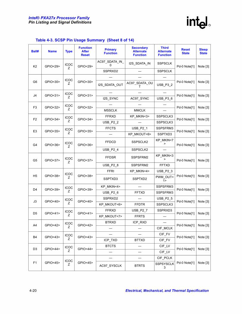
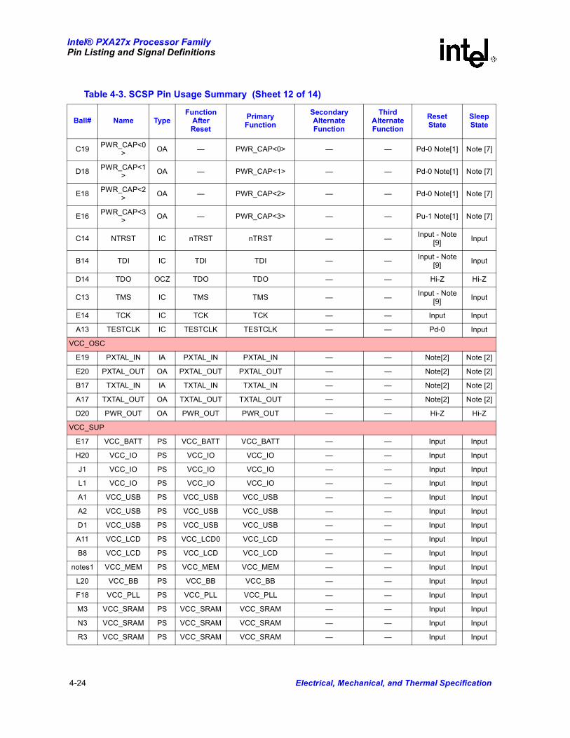
4.3 Pin Usage
Table 4-3 shows the Intel PXA27x processor pin-usage summary.
Table 4-3 does not include any of the Intel PXA27x flash and SDRAM dedicated signals. Review Table 4-1, Table 4-2, and Table 4-3 for ball location and mapping of memory signals.
Each signal’s alternate function inputs are shown in the upper section of each signal row and the outputs are shown in the lower section of each signal row. For example, GPIO<48> has a primary input function of CIF_DD<5> and a secondary output function of nPOE.
A18/A19/A20/B20/C20/C15/D19
Supply VSS VSS VSS VSS
W9/W12/W13/W16/Y15/Y18
RFU RFU — — —
Y14 Input NF_WP<1>1 — — —
NOTES:1. NF_WP<1> is reserved for a stacked data flash memory write protect pin (not yet available in current PXA27x
processor configurations), in the top package.2. Address signals within this table align with those found in the discrete flash datasheet. Address signals in the stacked
datasheet are shifted by one for 16-bit flash and by two for 32-bit flash to align the stack ballout for processor/system design.
Table 4-2. 2x256 Mbit(x32) (x16 each die) Flash - 1.8V (Sheet 4 of 4)
Ball# Type Ball Name Flash Die 1(L18)2 Flash Die 2(L18)2 PXA272
Table 4-3. SCSP Pin Usage Summary (Sheet 1 of 14)
Ball# Name TypeFunction
AfterReset
Primary Function
SecondaryAlternateFunction
ThirdAlternateFunction
ResetState
SleepState
VCC_MEM
V2 MA<25> OCZ MA<25> MA<25> — — Note[19] Note[19]
W2 MA<24> OCZ MA<24> MA<24> — — Note[19] Note[19]
W4 MA<23> OCZ MA<23> MA<23> — — Note[19] Note[19]
Y4 MA<22> OCZ MA<22> MA<22> — — Note[19] Note[19]
W5 MA<21> OCZ MA<21> MA<21> — — Note[19] Note[19]
T4 MA<20> OCZ MA<20> MA<20> — — Note[19] Note[19]
R4 MA<19> OCZ MA<19> MA<19> — — Note[19] Note[19]
P2 MA<18> OCZ MA<18> MA<18> — — Note[19] Note[19]
W6 MA<17> OCZ MA<17> MA<17> — — Note[19] Note[19]
T5 MA<16> OCZ MA<16> MA<16> — — Note[19] Note[19]

4-14 Electrical, Mechanical, and Thermal Specification
Intel® PXA27x Processor Family Pin Listing and Signal Definitions
R5 MA<15> OCZ MA<15> MA<15> — — Note[19] Note[19]
V6 MA<14> OCZ MA<14> MA<14> — — Note[19] Note[19]
U6 MA<13> OCZ MA<13> MA<13> — — Note[19] Note[19]
T6 MA<12> OCZ MA<12> MA<12> — — Note[19] Note[19]
W7 MA<11> OCZ MA<11> MA<11> — — Note[19] Note[19]
P4 MA<10> OCZ MA<10> MA<10> — — Note[19] Note[19]
P5 MA<9> OCZ MA<9> MA<9> — — Note[19] Note[19]
T7 MA<8> OCZ MA<8> MA<8> — — Note[19] Note[19]
R6 MA<7> OCZ MA<7> MA<7> — — Note[19] Note[19]
N5 MA<6> OCZ MA<6> MA<6> — — Note[19] Note[19]
W8 MA<5> OCZ MA<5> MA<5> — — Note[19] Note[19]
R7 MA<4> OCZ MA<4> MA<4> — — Note[19] Note[19]
P6 MA<3> OCZ MA<3> MA<3> — — Note[19] Note[19]
T8 MA<2> OCZ MA<2> MA<2> — — Note[19] Note[19]
Y3 MA<1> OCZ MA<1> MA<1> — — Note[19] Note[19]
W3 MA<0> OCZ MA<0> MA<0> — — Note[19] Note[19]
M5 MD<31>ICOC
ZMD<31> MD<31> — — Note[19] Note[19]
L5 MD<30>ICOC
ZMD<30> MD<30> — — Note[19] Note[19]
L6 MD<29>ICOC
ZMD<29> MD<29> — — Note[19] Note[19]
T9 MD<28>ICOC
ZMD<28> MD<28> — — Note[19] Note[19]
T10 MD<27>ICOC
ZMD<27> MD<27> — — Note[19] Note[19]
R11 MD<26>ICOC
ZMD<26> MD<26> — — Note[19] Note[19]
R12 MD<25>ICOC
ZMD<25> MD<25> — — Note[19] Note[19]
U13 MD<24>ICOC
ZMD<24> MD<24> — — Note[19] Note[19]
P15 MD<23>ICOC
ZMD<23> MD<23> — — Note[19] Note[19]
R15 MD<22>ICOC
ZMD<22> MD<22> — — Note[19] Note[19]
N15 MD<21>ICOC
ZMD<21> MD<21> — — Note[19] Note[19]
W14 MD<20>ICOC
ZMD<20> MD<20> — — Note[19] Note[19]
U15 MD<19>ICOC
ZMD<19> MD<19> — — Note[19] Note[19]
Table 4-3. SCSP Pin Usage Summary (Sheet 2 of 14)
Ball# Name TypeFunction
AfterReset
Primary Function
SecondaryAlternateFunction
ThirdAlternateFunction
ResetState
SleepState

Electrical, Mechanical, and Thermal Specification 4-15
Intel® PXA27x Processor FamilyPin Listing and Signal Definitions
T16 MD<18>ICOC
ZMD<18> MD<18> — — Note[19] Note[19]
N16 MD<17>ICOC
ZMD<17> MD<17> — — Note[19] Note[19]
N17 MD<16>ICOC
ZMD<16> MD<16> — — Note[19] Note[19]
N6 MD<15>ICOC
ZMD<15> MD<15> — — Note[19] Note[19]
M6 MD<14>ICOC
ZMD<14> MD<14> — — Note[19] Note[19]
R8 MD<13>ICOC
ZMD<13> MD<13> — — Note[19] Note[19]
R9 MD<12>ICOC
ZMD<12> MD<12> — — Note[19] Note[19]
R10 MD<11>ICOC
ZMD<11> MD<11> — — Note[19] Note[19]
T11 MD<10>ICOC
ZMD<10> MD<10> — — Note[19] Note[19]
T12 MD<9>ICOC
ZMD<9> MD<9> — — Note[19] Note[19]
R14 MD<8>ICOC
ZMD<8> MD<8> — — Note[19] Note[19]
V13 MD<7>ICOC
ZMD<7> MD<7> — — Note[19] Note[19]
T14 MD<6>ICOC
ZMD<6> MD<6> — — Note[19] Note[19]
M15 MD<5>ICOC
ZMD<5> MD<5> — — Note[19] Note[19]
M16 MD<4>ICOC
ZMD<4> MD<4> — — Note[19] Note[19]
V15 MD<3>ICOC
ZMD<3> MD<3> — — Note[19] Note[19]
P16 MD<2>ICOC
ZMD<2> MD<2> — — Note[19] Note[19]
M17 MD<1>ICOC
ZMD<1> MD<1> — — Note[19] Note[19]
U17 MD<0>ICOC
ZMD<0> MD<0> — — Note[19] Note[19]
W19 NOE OCZ nOE nOE — — Note[19] Note[19]
W20 NWE OCZ nWE nWE — — Note[19] Note[19]
Y19 NSDRAS OCZ nSDRAS nSDRAS — — Note[19] Note[19]
U20 NSDCAS OCZ nSDCAS nSDCAS — — Note[19] Note[19]
W18 DQM<0> OCZ DQM<0> DQM<0> — — Note[19] Note[19]
P17 DQM<1> OCZ DQM<1> DQM<1> — — Note[19] Note[19]
Table 4-3. SCSP Pin Usage Summary (Sheet 3 of 14)
Ball# Name TypeFunction
AfterReset
Primary Function
SecondaryAlternateFunction
ThirdAlternateFunction
ResetState
SleepState

4-16 Electrical, Mechanical, and Thermal Specification
Intel® PXA27x Processor Family Pin Listing and Signal Definitions
T17 DQM<2> OCZ DQM<2> DQM<2> — — Note[19] Note[19]
W17 DQM<3> OCZ DQM<3> DQM<3> — — Note[19] Note[19]
V18 NSDCS<0> OCZ nSDCS<0> nSDCS<0> — — Note[19] Note[19]
R17 NSDCS<1> OC nSDCS<1> nSDCS<1> — — Note[19] Note[19]
T18 SDCKE OC SDCKE SDCKE — — Note[19] Note[19]
V20 SDCLK<0> OC SDCLK<0> SDCLK<0> — — Note[19] Note[19]
P19 SDCLK<1> OCZ SDCLK<1> SDCLK<1> — — Note[19] Note[19]
T19 SDCLK<2> OC SDCLK<2> SDCLK<2> — — Note[19] Note[19]
V19 SDCLK<3> OC SDCLK<3> SDCLK<3> — — Note[19] Note[19]
M4 RDNWR OCZ RDnWR RDnWR — — Note[19] Note[19]
W1 NCS<0> OCZ nCS<0> nCS<0> — — Note[19] Note[19]
V1 GPIO<15>ICOC
ZGPIO<15>
— — —
Pu-1 Note[1] Note[4]nPCE<1>
nCS<1>
Note[19]—
M2 GPIO<18>ICOC
ZGPIO<18>
RDY — —Pd-0 Note[1] Note [3]
— — —
T20 GPIO<20>ICOC
ZGPIO<20>
DREQ<0> MBREQ —
Pu-1 Note[1] Note[3]nSDCS<2>
Note[19]— —
R18 GPIO<21>ICOC
ZGPIO<21>
— — —
Pu-1 Note[1] Note[3]nSDCS<3>
Note[19]DVAL<0> MBGNT
T3 GPIO<33>ICOC
ZGPIO<33>
FFRXD FFDSR —
Pu-1 Note[1] Note [4]DVAL<1>
nCS<5>
Note[19]MBGNT
M1 GPIO<49>ICOC
ZGPIO<49>
— — —
Pu-1 Note[1] Note [5]—
nPWE
Note[19]—
V4 GPIO<78>ICOC
ZGPIO<78>
— — —
Pu-1 Note[1] Note[4]nPCE<2>
nCS<2>
Note[19]—
P3 GPIO<79>ICOC
ZGPIO<79>
— — —
Pu-1 Note[1] Note[4]PSKTSEL
nCS<3>
Note[19]PWM_OUT<
2>
P1 GPIO<80>ICOC
ZGPIO<80>
DREQ<1> MBREQ —
Pu-1 Note[1] Note[4]—
nCS<4>
Note[19]PWM_OUT<
3>
Table 4-3. SCSP Pin Usage Summary (Sheet 4 of 14)
Ball# Name TypeFunction
AfterReset
Primary Function
SecondaryAlternateFunction
ThirdAlternateFunction
ResetState
SleepState

Electrical, Mechanical, and Thermal Specification 4-17
Intel® PXA27x Processor FamilyPin Listing and Signal Definitions
VCC_BB
L18 GPIO<48>ICOC
ZGPIO<48>
CIF_DD<5> — —
Pu-1 Note[1] Note [5]BB_OB_DAT<1>
nPOE
Note[19]—
K17 GPIO<50>ICOC
ZGPIO<50>
CIF_DD<3> —SSPSCLK<2
>Pu-1 Note[1] Note [5]
BB_OB_DAT<2>nPIOIR
Note[19]SSPSCLK<2
>
J15 GPIO<51>ICOC
ZGPIO<51>
CIF_DD<2> — —
Pu-1 Note[1] Note [5]BB_OB_DAT<3>
nPIOIW
Note[19]—
K18 GPIO<52>ICOC
ZGPIO<52>
CIF_DD<4> SSPSCLK<3> —Pd-0 Note[1] Note [3]
BB_OB_CLK SSPSCLK<3> —
K19 GPIO<53>ICOC
ZGPIO<53>
FFRXD USB_P2_3 —Pd-0 Note[1] Note [3]
BB_OB_STB CIF_MCLK SSPSYSCLK
K20 GPIO<54>ICOC
ZGPIO<54>
— BB_OB_WAIT CIF_PCLKPd-0 Note[1] Note [3]
nPCE<2> —
L16 GPIO<55>ICOC
ZGPIO<55>
CIF_DD<1> BB_IB_DAT<1> —Pu-1 Note[1] Note [5]
— nPREG —
M18 GPIO<56>ICOC
ZGPIO<56>
nPWAIT BB_IB_DAT<2> —Pu-1 Note[1] Note [5]
USB_P3_4 — —
L17 GPIO<57>ICOC
ZGPIO<57>
nIOIS16 BB_IB_DAT<3> —Pu-1 Note[1] Note [5]
— — SSPTXD
K15 GPIO<81>ICOC
ZGPIO<81>
— CIF_DD<0> —Pu-1 Note[1] Note [3]
SSPTXD3 BB_OB_DAT<0> —
N19 GPIO<82>ICOC
ZGPIO<82>
SSPRXD3 BB_IB_DAT<0> CIF_DD<5>Pu-1 Note[1] Note [3]
— — FFDTR
M19 GPIO<83>ICOC
ZGPIO<83>
SSPSFRM3 BB_IB_CLK CIF_DD<4>Pd-0 Note[1]] Note [3]
SSPSFRM3 FFTXD FFRTS
M20 GPIO<84>ICOC
ZGPIO<84>
SSPSCLK3 BB_IB_STB CIF_FVPd-0 Note[1] Note [3]
SSPSCLK3 — CIF_FV
L15 GPIO<85>ICOC
ZGPIO<85>
FFRXD DREQ<2> CIF_LVPd-0 Note[1] Note [3]
nPCE<1> BB_IB_WAIT CIF_LV
VCC_LCD
B12 GPIO<14>ICOC
ZGPIO<14>
L_VSYNC SSPSFRM2 —Pd-0 Note[1] Note [3]
— SSPSFRM2 UCLK
Table 4-3. SCSP Pin Usage Summary (Sheet 5 of 14)
Ball# Name TypeFunction
AfterReset
Primary Function
SecondaryAlternateFunction
ThirdAlternateFunction
ResetState
SleepState

4-18 Electrical, Mechanical, and Thermal Specification
Intel® PXA27x Processor Family Pin Listing and Signal Definitions
F14 GPIO<19>ICOC
ZGPIO<19>
SSPSCLK2 — FFRXDPd-0 Note[1] Note [3]
SSPSCLK2 L_CS nURST
D7 GPIO<58>ICOC
ZGPIO<58>
— LDD<0> —Pd-0 Note[1] Note [3]
— LDD<0> —
D8 GPIO<59>ICOC
ZGPIO<59>
— LDD<1> —Pd-0 Note[1] Note [3]
— LDD<1> —
F8 GPIO<60>ICOC
ZGPIO<60>
— LDD<2> —Pd-0 Note[1] Note [3]
— LDD<2> —
A8 GPIO<61>ICOC
ZGPIO<61>
— LDD<3> —Pd-0 Note[1] Note [3]
— LDD<3> —
E8 GPIO<62>ICOC
ZGPIO<62>
— LDD<4> —Pd-0 Note[1] Note [3]
— LDD<4> —
C8 GPIO<63>ICOC
ZGPIO<63>
— LDD<5> —Pd-0 Note[1] Note [3]
— LDD<5> —
C9 GPIO<64>ICOC
ZGPIO<64>
— LDD<6> —Pd-0 Note[1] Note [3]
— LDD<6> —
A9 GPIO<65>ICOC
ZGPIO<65>
— LDD<7> —Pd-0 Note[1] Note [3]
— LDD<7> —
E9 GPIO<66>ICOC
ZGPIO<66>
— LDD<8> —Pd-0 Note[1] Note [3]
— LDD<8> —
F10 GPIO<67>ICOC
ZGPIO<67>
— LDD<9> —Pd-0 Note[1] Note [3]
— LDD<9> —
D10 GPIO<68>ICOC
ZGPIO<68>
— LDD<10> —Pd-0 Note[1] Note [3]
— LDD<10> —
C10 GPIO<69>ICOC
ZGPIO<69>
— LDD<11> —Pd-0 Note[1] Note [3]
— LDD<11> —
B10 GPIO<70>ICOC
ZGPIO<70>
— LDD<12> —Pd-0 Note[1] Note [3]
— LDD<12> —
A10 GPIO<71>ICOC
ZGPIO<71>
— LDD<13> —Pd-0 Note[1] Note [3]
— LDD<13> —
E11 GPIO<72>ICOC
ZGPIO<72>
— LDD<14> —Pd-0 Note[1] Note [3]
— LDD<14> —
F12 GPIO<73>ICOC
ZGPIO<73>
— LDD<15> —Pd-0 Note[1] Note [3]
— LDD<15> —
E13 GPIO<74>ICOC
ZGPIO<74>
— — —Pd-0 Note[1] Note [3]
— L_FCLK_RD —
Table 4-3. SCSP Pin Usage Summary (Sheet 6 of 14)
Ball# Name TypeFunction
AfterReset
Primary Function
SecondaryAlternateFunction
ThirdAlternateFunction
ResetState
SleepState

Electrical, Mechanical, and Thermal Specification 4-19
Intel® PXA27x Processor FamilyPin Listing and Signal Definitions
C12 GPIO<75>ICOC
ZGPIO<75>
— — —Pd-0 Note[1] Note [3]
— L_LCLK _A0 —
D12 GPIO<76>ICOC
ZGPIO<76>
— — —Pd-0 Note[1] Note [3]
— L_PCLK_WR —
D13 GPIO<77>ICOC
ZGPIO<77>
— — —Pd-0 Note[1] Note [3]
— L_BIAS —
C11 GPIO<86>ICOC
ZGPIO<86>
SSPRXD2 LDD<16> USB_P3_5Pd-0 Note[1] Note [3]
nPCE<1> LDD<16> —
D11 GPIO<87>ICOC
ZGPIO<87>
nPCE<2> LDD<17> USB_P3_1Pd-0 Note[1] Note [3]
SSPTXD2 LDD<17> SSPSFRM2
VCC_IO
J6 GPIO<11>ICOC
ZGPIO<11>
EXT_SYNC<0> SSPRXD2 USB_P3_1Pd-0 Note[1]
Note [3],
Note[11CHOUT<0> PWM_OUT2 48_MHz
L3 GPIO<12>ICOC
ZGPIO<12>
EXT_SYNC<1> CIF_DD<7> —Pd-0 Note[1]
Note [3],
Note[11]CHOUT<1> PWM_OUT3 48_MHz
L4 GPIO<13>ICOC
ZGPIO<13>
CLK_EXT KP_DKIN<7>KP_MKIN<7
> Pd-0 Note[1]Note [3], Note[11]
SSPTXD2 — —
E6 GPIO<16>ICOC
ZGPIO<16>
KP_MKIN<5> — —Pd-0 Note[1] Note [3]
— PWM_OUT<0> FFTXD
G3 GPIO<17>ICOC
ZGPIO<17>
KP_MKIN<6> CIF_DD<6> —Pd-0 Note[1] Note [3]
— PWM_OUT<1> —
F7 GPIO<22>ICOC
ZGPIO<22>
SSPEXTCLK2 SSPSCLKEN2 SSPSCLK2Pd-0 Note[1] Note [3]
KP_MKOUT<7> SSPSYSCLK2 SSPSCLK2
H1 GPIO<23>ICOC
ZGPIO<23>
— SSPSCLK —Pd-0 Note[1] Note [3]
CIF_MCLK SSPSCLK —
H2 GPIO<24>ICOC
ZGPIO<24>
CIF_FV SSPSFRM —Pd-0 Note[1] Note [3]
CIF_FV SSPSFRM —
F6 GPIO<25>ICOC
ZGPIO<25>
CIF_LV — —Pd-0 Note[1] Note [3]
CIF_LV SSPTXD —
H3 GPIO<26>ICOC
ZGPIO<26>
SSPRXD CIF_PCLK FFCTS Pd-0 Note[1] Note [3]
— — —
H4 GPIO<27>ICOC
ZGPIO<27>
SSPEXTCLK SSPSCLKEN CIF_DD<0>Pd-0 Note[1] Note [3]
SSPSYSCLK — FFRTS
K1 GPIO<28> ICOC
ZGPIO<28>
AC97_BITCLK I2S_BITCLK SSPSFRMPd-0 Note[1] Note [3]
I2S_BITCLK — SSPSFRM
Table 4-3. SCSP Pin Usage Summary (Sheet 7 of 14)
Ball# Name TypeFunction
AfterReset
Primary Function
SecondaryAlternateFunction
ThirdAlternateFunction
ResetState
SleepState
4-20 Electrical, Mechanical, and Thermal Specification
Intel® PXA27x Processor Family Pin Listing and Signal Definitions
K2 GPIO<29>ICOC
ZGPIO<29>
AC97_SDATA_IN_0
I2S_SDATA_IN SSPSCLKPd-0 Note[1] Note [3]
SSPRXD2 — SSPSCLK
G6 GPIO<30>ICOC
ZGPIO<30>
— — —
Pd-0 Note[1] Note [3]I2S_SDATA_OUT
AC97_SDATA_OUT
USB_P3_2
J4 GPIO<31>ICOC
ZGPIO<31>
— — —Pd-0 Note[1] Note [3]
I2S_SYNC AC97_SYNC USB_P3_6
F3 GPIO<32>ICOC
ZGPIO<32>
— — —Pd-0 Note[1] Note [3]
MSSCLK MMCLK —
F2 GPIO<34>ICOC
ZGPIO<34>
FFRXD KP_MKIN<3> SSPSCLK3Pd-0 Note[1] Note [3]
USB_P2_2 — SSPSCLK3
E3 GPIO<35> ICOC
ZGPIO<35>
FFCTS USB_P2_1 SSPSFRM3Pd-0 Note[1] Note [3]
— KP_MKOUT<6> SSPTXD3
G4 GPIO<36>ICOC
ZGPIO<36>
FFDCD SSPSCLK2KP_MKIN<7
> Pd-0 Note[1] Note [3]
USB_P2_4 SSPSCLK2 —
G5 GPIO<37>ICOC
ZGPIO<37>
FFDSR SSPSFRM2KP_MKIN<3
> Pd-0 Note[1] Note [3]
USB_P2_8 SSPSFRM2 FFTXD
H5 GPIO<38>ICOC
ZGPIO<38>
FFRI KP_MKIN<4> USB_P2_3
Pd-0 Note[1] Note [3]SSPTXD3 SSPTXD2
PWM_OUT<1>
D4 GPIO<39> ICOC
ZGPIO<39>
KP_MKIN<4> — SSPSFRM3Pd-0 Note[1] Note [3]
USB_P2_6 FFTXD SSPSFRM3
J3 GPIO<40>ICOC
ZGPIO<40>
SSPRXD2 — USB_P2_5Pd-0 Note[1] Note [3]
KP_MKOUT<6> FFDTR SSPSCLK3
D5 GPIO<41>ICOC
ZGPIO<41>
FFRXD USB_P2_7 SSPRXD3Pd-0 Note[1] Note [3]
KP_MKOUT<7> FFRTS —
A4 GPIO<42> ICOC
ZGPIO<42>
BTRXD ICP_RXD —Pd-0 Note[1] Note [3]
— — CIF_MCLK
B4 GPIO<43>ICOC
ZGPIO<43>
— — CIF_FVPd-0 Note[1] Note [3]
ICP_TXD BTTXD CIF_FV
D3 GPIO<44> ICOC
ZGPIO<44>
BTCTS — CIF_LVPd-0 Note[1] Note [3]
— — CIF_LV
F1 GPIO<45> ICOC
ZGPIO<45>
— — CIF_PCLK
Pd-0 Note[1] Note [3]AC97_SYSCLK BTRTS
SSPSYSCLK3
Table 4-3. SCSP Pin Usage Summary (Sheet 8 of 14)
Ball# Name TypeFunction
AfterReset
Primary Function
SecondaryAlternateFunction
ThirdAlternateFunction
ResetState
SleepState

Electrical, Mechanical, and Thermal Specification 4-21
Intel® PXA27x Processor FamilyPin Listing and Signal Definitions
H6 GPIO<46>ICOC
ZGPIO<46>
ICP_RXD STD_RXD —Pd-0 Note[1] Note [3]
— PWM_OUT<2> —
K5 GPIO<47>ICOC
ZGPIO<47>
CIF_DD<0> — —
Pd-0 Note[1] Note [3]STD_TXD ICP_TXD
PWM_OUT<3>
B3 GPIO<88>ICOC
ZGPIO<88>
USBHPWR<1> SSPRXD2 SSPSFRM2Pd-0 Note[1] Note [3]
— — SSPSFRM2
A3 GPIO<89>ICOC
ZGPIO<89>
SSPRXD3 — FFRIPd-0 Note[1] Note [3]
AC97_SYSCLK USBHPEN<1> SSPTXD2
G2 GPIO<92>ICOC
ZGPIO<92>
MMDAT<0> — —Pd-0 Note[1] Note [3]
MMDAT<0> MSBS —
G19 GPIO<93>ICOC
ZGPIO<93>
KP_DKIN<0> CIF_DD<6> —
Pd-0 Note[1] Note [3]AC97_SDATA_OUT
— —
F16 GPIO<94>ICOC
ZGPIO<94>
KP_DKIN<1> CIF_DD<5> —Pd-0 Note[1] Note [3]
AC97_SYNC — —
G20 GPIO<95>ICOC
ZGPIO<95>
KP_DKIN<2> CIF_DD<4>KP_MKIN<6
> Pd-0 Note[1] Note [3]
AC97_RESET_n — —
F17 GPIO<96>ICOC
ZGPIO<96>
KP_DKIN<3> MBREQ FFRXD
Pd-0 Note[1] Note [3]DVAL<1>
KP_MKOUT<6>
F15 GPIO<97>ICOC
ZGPIO<97>
KP_DKIN<4> DREQ<1>KP_MKIN<3
> Pd-0 Note[1] Note [3]
— MBGNT —
G18 GPIO<98>ICOC
ZGPIO<98>
KP_DKIN<5> CIF_DD<0>KP_MKIN<4
> Pd-0 Note [3]
AC97_SYSCLK — FFRTS
G17 GPIO<99>ICOC
ZGPIO<99>
KP_DKIN<6>AC97_SDATA_IN_
1KP_MKIN<5
> Pd-0 Note [3]
— — FFTXD
G16 GPIO<100>ICOC
ZGPIO<100>
KP_MKIN<0> DREQ<2> FFCTSPd-0 Note[1] Note [3]
— — —
H18 GPIO<101>ICOC
ZGPIO<101>
KP_MKIN<1> — —Pd-0 Note[1] Note [3]
— — —
H19 GPIO<102>ICOC
ZGPIO<102>
KP_MKIN<2> — FFRXDPd-0 Note[1] Note [3]
nPCE<1> — —
J20 GPIO<103>ICOC
ZGPIO<103>
CIF_DD<3> — —Pd-0 Note[1] Note [3]
— KP_MKOUT<0> —
Table 4-3. SCSP Pin Usage Summary (Sheet 9 of 14)
Ball# Name TypeFunction
AfterReset
Primary Function
SecondaryAlternateFunction
ThirdAlternateFunction
ResetState
SleepState

4-22 Electrical, Mechanical, and Thermal Specification
Intel® PXA27x Processor Family Pin Listing and Signal Definitions
H17 GPIO<104>ICOC
ZGPIO<104>
CIF_DD<2> — —Pd-0 Note[1] Note [3]
PSKTSEL KP_MKOUT<1> —
J18 GPIO<105>ICOC
ZGPIO<105>
CIF_DD<1> — —Pd-0 Note[1] Note [3]
nPCE<2> KP_MKOUT<2> —
H16 GPIO<106>ICOC
ZGPIO<106>
CIF_DD<9> — —Pd-0 Note[1] Note [3]
— KP_MKOUT<3> —
J17 GPIO<107>ICOC
ZGPIO<107>
CIF_DD<8> — —Pd-0 Note[1] Note [3]
— KP_MKOUT<4> —
J16 GPIO<108>ICOC
ZGPIO<108>
CIF_DD<7> — —Pd-0 Note[1] Note [3]
CHOUT<0> KP_MKOUT<5> —
E5 GPIO<109>ICOC
ZGPIO<109>
MMDAT<1> MSSDIO —Pd-0 Note[1] Note [3]
MMDAT<1> MSSDIO —
F4 GPIO<110>ICOC
ZGPIO<110>
MMDAT<2>/MMCCS<0>
— —
Pd-0 Note[1] Note [3]MMDAT<2>/MMCCS<0>
— —
F5 GPIO<111>ICOC
ZGPIO<111>
MMDAT<3>/MMCCS<1>
— —
Pd-0 Note[1] Note [3]MMDAT<3>/MMCCS<1>
— —
G1 GPIO<112>ICOC
ZGPIO<112>
MMCMD nMSINS —Pd-0 Note[1] Note [3]
MMCMD — —
K4 GPIO<113>ICOC
ZGPIO<113>
— — USB_P3_3Pd-0 Note[1] Note [3]
I2S_SYSCLK AC97_RESET_n —
C5GPIO<114>
Note [17]ICOC
ZGPIO<114>
Note [17]
CIFDD_<1> — —Pd-0 Note[1] Note [3]
UVS0 —
B5GPIO<115>
Note [17]ICOC
ZGPIO<115>
Note [17]
DREQ<0> CIF_DD<3> MBREQ
Pu-1 Note[1] Note [3]UEN nUVS1
PWM_OUT<1>
C4 GPIO<116>ICOC
ZGPIO<116>
CIF_DD<2>AC97_SDATA_IN_
0UDET
Pu-1 Note[1] Note [3]
DVAL<0> nUVS2 MBGNT
E2 GPIO<117>ICOC
ZGPIO<117>
SCL — —Pu-1 Note[1]
Note [3],
Note[12]SCL — —
B1 GPIO<118> ICOC
ZGPIO<118>
SDA — —Pu-1 Note[1]
Note [3],
Note[12]SDA — —
B2 GPIO<119>ICOC
ZGPIO<119>
USBHPWR<2> — —Pd-0 Note[1] Note [3]
— — —
Table 4-3. SCSP Pin Usage Summary (Sheet 10 of 14)
Ball# Name TypeFunction
AfterReset
Primary Function
SecondaryAlternateFunction
ThirdAlternateFunction
ResetState
SleepState

Electrical, Mechanical, and Thermal Specification 4-23
Intel® PXA27x Processor FamilyPin Listing and Signal Definitions
C3 GPIO<120>ICOC
ZGPIO<120>
— — —Pd-0 Note[1] Note [3]
— USBHPEN<2> —
VCC_USB
D2 USBC_P IAOAZ USBC_P USBC_P — — Hi-Z Hi-Z
C2 USBC_N IAOAZ USBC_N USBC_N — — Hi-Z Hi-Z
A6 USBH_P<1> IAOAZ USBH_P<1> USBH_P<1> — — Hi-Z Hi-Z
A5 USBH_N<1> IAOAZ USBH_N<1> USBH_N<1> — — Hi-Z Hi-Z
VCC_USIM
A7 GPIO<90>ICOC
ZGPIO<90>
KP_MKIN<5> USB_P3_5 CIF_DD<4>Pd-0 Note[1] Note [3]
— nURST —
C7 GPIO<91>ICOC
ZGPIO<91>
KP_MKIN<6> USB_P3_1 CIF_DD<5>Pd-0 Note[1] Note [3]
— UCLK —
B6 UIOICOC
ZUIO UIO — — Driven Low Hi-Z
VCC_REG
A15 GPIO<0>ICOC
ZGPIO<0> GPIO<0> — — Pd-0 Note[1] Note [3]
D16 GPIO<1>ICOC
ZGPIO<1> GPIO<1> — — Pu-1 Note[1] Note [7]
C16 GPIO<3>ICOC
ZGPIO<3> PWR_SCL — — Pu-1 Note[1] Hi-Z
B15 GPIO<4>ICOC
ZGPIO<4> PWR_SDA — — Pu-1 Note[1] Hi-Z
A14GPIO<9>
Note [18]ICOC
ZGPIO<9>
Note [18]
— — FFCTSPd-0 Note[1]
Note [7,18]HZ_CLK — CHOUT<0>
D15GPIO<10>
Note [18]ICOC
ZGPIO<10>
Note [18]
FFDCD — USB_P3_5Pd-0 Note[1]
Note [7,18]HZ_CLK — CHOUT<1>
E15 CLK_REQICOC
ZCLK_REQ CLK_REQ — — Pu-1 Note [8]
A16 NRESET IC nRESET nRESET — —Input - Note
[9]Input
B19NRESET_OU
TOC
nRESET_OUT
nRESET_OUT — — Low Note [8]
B18 BOOT_SEL IC BOOT_SEL BOOT_SEL — — Input Input
B16 PWR_EN OC PWR_EN PWR_EN — — Note[16] Note [8]
C18NBATT_FAUL
TIC
nBATT_FAULT
nBATT_FAULT — — Low Input
C17NVDD_FAUL
TIC nVDD_FAULT nVDD_FAULT — — Low Input
D17 SYS_ENICOC
ZSYS_EN SYS_EN — — Pu-1 Note[1] Note [7]
Table 4-3. SCSP Pin Usage Summary (Sheet 11 of 14)
Ball# Name TypeFunction
AfterReset
Primary Function
SecondaryAlternateFunction
ThirdAlternateFunction
ResetState
SleepState
4-24 Electrical, Mechanical, and Thermal Specification
Intel® PXA27x Processor Family Pin Listing and Signal Definitions
C19PWR_CAP<0
>OA — PWR_CAP<0> — — Pd-0 Note[1] Note [7]
D18PWR_CAP<1
>OA — PWR_CAP<1> — — Pd-0 Note[1] Note [7]
E18PWR_CAP<2
>OA — PWR_CAP<2> — — Pd-0 Note[1] Note [7]
E16PWR_CAP<3
>OA — PWR_CAP<3> — — Pu-1 Note[1] Note [7]
C14 NTRST IC nTRST nTRST — —Input - Note
[9]Input
B14 TDI IC TDI TDI — —Input - Note
[9]Input
D14 TDO OCZ TDO TDO — — Hi-Z Hi-Z
C13 TMS IC TMS TMS — —Input - Note
[9]Input
E14 TCK IC TCK TCK — — Input Input
A13 TESTCLK IC TESTCLK TESTCLK — — Pd-0 Input
VCC_OSC
E19 PXTAL_IN IA PXTAL_IN PXTAL_IN — — Note[2] Note [2]
E20 PXTAL_OUT OA PXTAL_OUT PXTAL_OUT — — Note[2] Note [2]
B17 TXTAL_IN IA TXTAL_IN TXTAL_IN — — Note[2] Note [2]
A17 TXTAL_OUT OA TXTAL_OUT TXTAL_OUT — — Note[2] Note [2]
D20 PWR_OUT OA PWR_OUT PWR_OUT — — Hi-Z Hi-Z
VCC_SUP
E17 VCC_BATT PS VCC_BATT VCC_BATT — — Input Input
H20 VCC_IO PS VCC_IO VCC_IO — — Input Input
J1 VCC_IO PS VCC_IO VCC_IO — — Input Input
L1 VCC_IO PS VCC_IO VCC_IO — — Input Input
A1 VCC_USB PS VCC_USB VCC_USB — — Input Input
A2 VCC_USB PS VCC_USB VCC_USB — — Input Input
D1 VCC_USB PS VCC_USB VCC_USB — — Input Input
A11 VCC_LCD PS VCC_LCD0 VCC_LCD — — Input Input
B8 VCC_LCD PS VCC_LCD VCC_LCD — — Input Input
notes1 VCC_MEM PS VCC_MEM VCC_MEM — — Input Input
L20 VCC_BB PS VCC_BB VCC_BB — — Input Input
F18 VCC_PLL PS VCC_PLL VCC_PLL — — Input Input
M3 VCC_SRAM PS VCC_SRAM VCC_SRAM — — Input Input
N3 VCC_SRAM PS VCC_SRAM VCC_SRAM — — Input Input
R3 VCC_SRAM PS VCC_SRAM VCC_SRAM — — Input Input
Table 4-3. SCSP Pin Usage Summary (Sheet 12 of 14)
Ball# Name TypeFunction
AfterReset
Primary Function
SecondaryAlternateFunction
ThirdAlternateFunction
ResetState
SleepState

Electrical, Mechanical, and Thermal Specification 4-25
Intel® PXA27x Processor FamilyPin Listing and Signal Definitions
U3 VCC_SRAM PS VCC_SRAM VCC_SRAM — — Input Input
A12 VCC_CORE PS VCC_CORE VCC_CORE — — Input Input
B7 VCC_CORE PS VCC_CORE VCC_CORE — — Input Input
B9 VCC_CORE PS VCC_CORE VCC_CORE — — Input Input
B11 VCC_CORE PS VCC_CORE VCC_CORE — — Input Input
E1 VCC_CORE PS VCC_CORE VCC_CORE — — Input Input
J19 VCC_CORE PS VCC_CORE VCC_CORE — — Input Input
K3 VCC_CORE PS VCC_CORE VCC_CORE — — Input Input
L19 VCC_CORE PS VCC_CORE VCC_CORE — — Input Input
R2 VCC_CORE PS VCC_CORE VCC_CORE — — Input Input
R20 VCC_CORE PS VCC_CORE VCC_CORE — — Input Input
T13 VCC_CORE PS VCC_CORE VCC_CORE — — Input Input
T15 VCC_CORE PS VCC_CORE VCC_CORE — — Input Input
U1 VCC_CORE PS VCC_CORE VCC_CORE — — Input Input
C6 VCC_USIM PS VCC_USIM VCC_USIM — — Input Input
notes2 VSS PS VSS VSS — — Input Input
D6 VSS_IO PS VSS_IO VSS_IO — — Input Input
D9 VSS_IO PS VSS_IO VSS_IO — — Input Input
E4 VSS_IO PS VSS_IO VSS_IO — — Input Input
E12 VSS_IO PS VSS_IO VSS_IO — — Input Input
F20 VSS_IO PS VSS_IO VSS_IO — — Input Input
G15 VSS_IO PS VSS_IO VSS_IO — — Input Input
J2 VSS_IO PS VSS_IO VSS_IO — — Input Input
L2 VSS_IO PS VSS_IO VSS_IO — — Input Input
B13 VSS_IO PS VSS_IO VSS_IO — — Input Input
notes3 VSS_MEM PS VSS_MEM VSS_MEM — — Input Input
K16 VSS_BB PS VSS_BB VSS_BB — — Input Input
F19 VSS_PLL PS VSS_PLL VSS_PLL — — Input Input
R13 VSS_CORE PS VSS_CORE VSS_CORE — — Input Input
R16 VSS_CORE PS VSS_CORE VSS_CORE — — Input Input
U2 VSS_CORE PS VSS_CORE VSS_CORE — — Input Input
U4 VSS_CORE PS VSS_CORE VSS_CORE — — Input Input
U18 VSS_CORE PS VSS_CORE VSS_CORE — — Input Input
V3 VSS_CORE PS VSS_CORE VSS_CORE — — Input Input
Y1 VSS_CORE PS VSS_CORE VSS_CORE — — Input Input
C1 VSS_CORE PS VSS_CORE VSS_CORE — — Input Input
Table 4-3. SCSP Pin Usage Summary (Sheet 13 of 14)
Ball# Name TypeFunction
AfterReset
Primary Function
SecondaryAlternateFunction
ThirdAlternateFunction
ResetState
SleepState

4-26 Electrical, Mechanical, and Thermal Specification
Intel® PXA27x Processor Family Pin Listing and Signal Definitions
E7 VSS_CORE PS VSS_CORE VSS_CORE — — Input Input
E10 VSS_CORE PS VSS_CORE VSS_CORE — — Input Input
F9 VSS_CORE PS VSS_CORE VSS_CORE — — Input Input
F11 VSS_CORE PS VSS_CORE VSS_CORE — — Input Input
F13 VSS_CORE PS VSS_CORE VSS_CORE — — Input Input
H15 VSS_CORE PS VSS_CORE VSS_CORE — — Input Input
J5 VSS_CORE PS VSS_CORE VSS_CORE — — Input Input
K6 VSS_CORE PS VSS_CORE VSS_CORE — — Input Input
N4 VSS_CORE PS VSS_CORE VSS_CORE — — Input Input
NOTES:1. 2. 3. Refer to PXA27x Processor Mapping Table for VCC_MEM, VSS_MEM and VSS ball location
Table 4-3. SCSP Pin Usage Summary (Sheet 14 of 14)
Ball# Name TypeFunction
AfterReset
Primary Function
SecondaryAlternateFunction
ThirdAlternateFunction
ResetState
SleepState

Electrical, Mechanical, and Thermal Specification 4-27
Intel® PXA27x Processor FamilyPin Listing and Signal Definitions
4.4 Signal Types
Table 4-4. Pin Usage and Mapping Notes
Note Description
[1]
GPIO reset/deep sleep operation: After any reset is asserted or if the Intel PXA27x processor is in deep-sleep mode, these pins are configured as GPIO inputs by default. The input buffers for these pins are disabled to prevent current drain and must be enabled prior to use by clearing the read-disable hold bit, PSSR[RDH]. Until RDH is cleared, each pin is pulled high (Pu-1), pulled low (Pd-0), or floated (Hi-Z).
[2]Crystal oscillator pins: These pins connect the external crystals to the on-chip oscillators and are not affected by either reset or sleep. For more information, see the “Clocks and Power” chapter in the Intel® PXA27x Processor Family Developer’s Manual.
[3]
GPIO sleep operation: During the transition into sleep mode, the configuration of these pins is determined by the corresponding GPIO setting. This pin is not driven during sleep if the direction of the pin is selected as an input. If the direction of the pin is selected as an output, the value contained in the Power Manager GPIO Sleep-State register (PGSR0/1/2/3) is driven out onto the pin and held while the processor is in sleep mode.
Upon exit from sleep mode, GPIOs that are configured as outputs continue to hold the standby, sleep, or deep-sleep state until software clears the peripheral-control hold bit, PSSR[PH]. Software must clear this bit (by writing 0b1 to it) after the peripherals have been fully configured, as described in Note[1], but before the process actually uses them.
GPIOs that are configured as inputs immediately after exiting sleep mode cannot be used until PSSR[RDH] is cleared.
[4]
Static memory control pins: During sleep mode, these pins can be programmed either to drive the value in the Power Manager GPIO Sleep-State register (PGSR0/1/2/3) or to be placed in a Hi-Z (undriven) state. To select the Hi-Z state, software must set PCFR[FS]. If FS is not set, these pins function as described in Note[3] during the transition to sleep mode.
[5]PCMCIA control pins: During sleep mode, these pins can be programmed either to drive the value in the Power Manager GPIO Sleep-State register (PGSR0/1/2/3) or to be placed in a Hi-Z (undriven) state. To select the Hi-Z state, software must set PCFR[FP]. If FP is not set, these pins function as described in Note[3] during the transition to sleep mode.
[6] (reserved)
[7]When the power manager overrides the GPIO alternate function, the Power Manager GPIO Sleep-State registers (PGSR0/1/2/3) and the PSSR[RDH] bit are ignored. Pullup and pulldown are disabled immediately after the power manager overrides the GPIO function.
[8] Output functions during sleep mode
[9] Pull-up always enabled
[10] (reserved)
[11] Pins do not function during sleep mode if the OS timer is active
[12] Pins must be floated by software during sleep mode (floating does not happen automatically)
[13] (reserved)
[14] (reserved)
[15]The pin is three-stateable (Hi-Z) based on the value of PCFR[FS]. There is no PGSR0/1/2/3 setting associated with the pin because it is not a GPIO.
[16]PWR_EN goes high during reset, between the assertion of the reset pin and the de-assertion of internal reset within the Intel PXA27x processor, after SYS_EN is driven high.
[17]GPIOs 114 and115: The alternate function configuration of these pins is ignored when either PUCR[USIM114] or PUCR[USIM115] bits are set. Setting these bits forces the USIM enable signal onto these GPIOs.
[18]When software sets the OSCC[PIO_EN] or OSCC[TOUT_EN] bits, then any GPIO alternate function setting applied to GPIO<9> or GPIO <10> is overridden with the CLK_PIO function on GPIO<9> and CLK_TOUT on GPIO<10>.
[19] Refer to Table 4-6.

4-28 Electrical, Mechanical, and Thermal Specification
Intel® PXA27x Processor Family Pin Listing and Signal Definitions
4.5 Memory Controller Reset and Initialization
The SDRAM interface is disabled on reset. Reset values for the boot ROM are determined by BOOT_SEL (see the Intel® PXA27x Processor Family Developers Manual, Memory Controller chapter). Boot ROM is immediately available for reading upon exit from reset, and all memory interface control registers are available for writing.
On hardware reset, the memory pins and controller are in the state shown in Table 4-6.
Table 4-5. Signal Types
Type Description
IC CMOS input
OC CMOS output
OCZ CMOS output, three-stateable
ICOCZ CMOS bidirectional, three-stateable
IA Analog input
OA Analog output
IAOA Analog bidirectional
IAOAZ Analog bidirectional - three-stateable
PS Power supply
Table 4-6. Memory Controller Pin Reset Values (Sheet 1 of 2)
Pin NameReset, Sleep, Standby, Deep-Sleep, Frequency Change, and Manual Self-Refresh Mode Values
SDCLK <31:0> 0b000
SDCKE 0
DQM <3:0> 0b0000
nSDCS <3:2> GPIO (memory controller drives 0b11)†
nSDCS <1:0> 0b11
nWE 1
nSDRAS 1
nSDCAS 1
nOE 1
MA <25:0> 0x0000_00001
RDnWR 0
MD <31:0> 0x0000_00002
nCS <0> 1
nCS <5:1> GPIO (memory controller drives 0b11111)
nPIOIR GPIO (memory controller drives high)
nPIOIW GPIO (memory controller drives high)

Electrical, Mechanical, and Thermal Specification 4-29
Intel® PXA27x Processor FamilyPin Listing and Signal Definitions
The address signals are driven low and data signals are pulled low during sleep, standby, deep-sleep, frequency-change modes, and manual self-refresh. All other memory control signals are in the same state that they are in after a hardware reset. If the SDRAMs are in self-refresh mode, they are kept there by driving SDCKE low.
4.6 Power-Supply Pins
Table 4-7 summarizes the power-supply ball count.
§§
nPOE GPIO (memory controller drives high)
nPWE GPIO (memory controller drives high)
NOTE:
† This indicates that the GPIO pin, if configured for the alternate function used by the memory controller during reset, drives the represented value.
NOTE: SCLK<3> is only available on PXA27x processor family packages1. MA pins are driven 2. MD pins are pulled low
Table 4-6. Memory Controller Pin Reset Values (Sheet 2 of 2)
Pin NameReset, Sleep, Standby, Deep-Sleep, Frequency Change, and Manual Self-Refresh Mode Values
Table 4-7. SCSP 1.8V Power Supply Pin Summary
Name Number of Package Balls
VCC_BATT 1
VCC_IO 3
VCC_USB 3
VCC_LCD 2
VCC_MEM 24
VCC_BB 1
VCC_PLL 1
VCC_SRAM 4
VCC_CORE 13
VCC_USIM 1
VSS 7
VSS_IO 9
VSS_MEM 19
VSS_BB 1
VSS_PLL 1
VSS_CORE 17
4-30 Electrical, Mechanical, and Thermal Specification
Intel® PXA27x Processor Family Pin Listing and Signal Definitions

Electrical, Mechanical, and Thermal Specification 5-1
Electrical Specifications 5
5.1 Absolute Maximum Ratings
The absolute maximum ratings (shown in Table 5-1) define limitations for electrical and thermal stresses. These limits prevent permanent damage to the Intel PXA27x processor family.
Note: Absolute maximum ratings are not operating ranges.
5.2 Operating Conditions
This section shows operating voltage, frequency, and temperature specifications for the PXA27x processor.
Table 5-1. Absolute Maximum Ratings
Symbol Description Min Max Units
TS Storage temperature –40 125 °C
VCC_OL1Offset voltage between any of the following pins:
VCC_CORE–0.3 0.3 V
VCC_OL2Offset voltage between any of the following pins:
VCC_SRAM–0.3 0.3 V
VCC_OH1Offset voltage between any of the following pins:
VCC_MEM–0.3 0.3 V
VCC_OH2Offset voltage between any of the following pins:
VCC_IO–0.3 0.3 V
VCC_OH3 Offset voltage between VCC_LCD<0> and VCC_LCD<1> –0.3 0.3 V
VCC_HV
Voltage applied to high-voltage supply pins(VCC_BB, VCC_USIM, VCC_MEM, VCC_IO<, VCC_LCD)
VSS–0.3 VSS+4.0 V
VCC_LVVoltage applied to low-voltage supply pins(VCC_CORE, VCC_PLL, VCC_SRAM)
VSS–0.3 VSS+1.45 V
VIPVoltage applied to non-supply pins except PXTAL_IN, PXTAL_OUT, TXTAL_IN, and TXTAL_OUT pins
VSS–0.3 VSS+4.0 V
VIP_XVoltage applied to XTAL pins(PXTAL_IN, PXTAL_OUT, TXTAL_IN, TXTAL_OUT)
VSS–0.3 VSS+1.45 V
VESD
Maximum ESD stress voltage, three stresses maximum:
• Any pin to any supply pin, either polarity, or
• Any pin to all non-supply pins together, either polarity
— 2000 V
IEOSMaximum DC input current (electrical overstress) for any non-supply pin
— 5 mA

5-2 Electrical, Mechanical, and Thermal Specification
Intel® PXA27x Processor Family Electrical Specifications
Table 5-2 shows each power domains supported voltages (except for VCC_MEM and VCC_CORE). Table 5-3 shows all of the supported memory voltages and frequency operating ranges (VCC_MEM). Table Note: shows all of the supported core voltage and frequency ranges (VCC_CORE).
The operating temperature specification is a function of voltage and frequency.
Table 5-2. Voltage, Temperature, and Frequency Electrical Specifications (Sheet 1 of 2)
Symbol Description Min Typical Max Units
Operating Temperature
Tcase Package operating temperature† -25 — +85 °C
Theta Jc Junction-to-case temperature gradient — 2 —°C/ watt
VCC_BATT Voltage
VVCC0 Voltage applied on VCC_BATT @3.0V 2.25 3.00 3.75 V
VVDF1
Voltage difference between VCC_BATT and VCC_IO during power-on reset or deep-sleep wake-up (from the assertion of SYS_EN to the de-assertion of nRESET_OUT)
0 — 0.30 V
VVDF2Voltage difference between VCC_BATT and VCC_IO when VCC_IO is enabled
0 — 0.20 V
Tbramp Ramp Rate — 10 12 mV/uS
VCC_PLL Voltage
VVCC1Voltage applied on VCC_PLL @1.3V
(+10/-10%)1.17 1.30 1.43 V
Tpwrramp Ramp Rate — 10 12 mV/uS
VCC_BB Voltages
VVCC2aVoltage applied on VCC_BB @1.8V
(+20/-5%)1.71 1.80 2.16 V
VVCC2bVoltage applied on VCC_BB @2.5V
(+10/-10%)2.25 2.50 2.75 V
VVCC2cVoltage applied on VCC_BB @3.0V
(+10/-10%)2.70 3.0 3.30 V
VVCC2dVoltage applied on VCC_BB @3.3V
(+10/-10%)2.97 3.3 3.63 V
Tsysramp Ramp Rate — 10 12 mV/uS
NOTE: VCC_BB may optionally be tied to the same PMIC as VCC_IO if the system design allows both VCC_IO and VCC_BB to use the same logic level. This allows the GPIOs on VCC_BB to be used at the same voltage level.
VCC_LCD Voltages
VVCC3aVoltage applied on VCC_LCD @1.8V
(+20/-5%)1.71 1.80 2.16 V
VVCC3bVoltage applied on VCC_LCD @2.5V
(+10/-10%)2.25 2.50 2.75 V

Electrical, Mechanical, and Thermal Specification 5-3
Intel® PXA27x Processor FamilyElectrical Specifications
Table 5-3 shows the supported memory frequency and memory supply voltage operating ranges for the Intel PXA27x processor.
Note: Do not exceed top-package specifications. Refer to the appropriate top-package data sheets for top- package specifications.
VVCC3cVoltage applied on VCC_LCD @3.0V
(+10/-10%)2.70 3.0 3.30 V
VVCC3dVoltage applied on VCC_LCD @3.3V
(+10/-10%)2.97 3.3 3.63 V
Tsysramp Ramp Rate — 10 12 mV/uS
VCC_IO Voltages
VVCC4aVoltage applied on VCC_IO @3.0V
(+10/-10.3%)2.69175 3.0 3.30 V
VVCC4bVoltage applied on VCC_IO @3.3V
(+10/-10%)2.97 3.3 3.63 V
Tsysramp Ramp Rate — 10 12 mV/uS
NOTE: VCC_IO must be maintained at a voltage as high as or higher than, all other supplies except for VCC_BATT and VCC_USB
VCC_USIM Voltages
VVCC5aVoltage applied on VCC_USIM @1.8V
(+20/-5%)1.71 1.80 2.16 V
VVCC5bVoltage applied on VCC_USIM @3.0V
(+10/-10%)2.70 3.0 3.30 V
Tsysramp Ramp Rate — 10 12 mV/uS
NOTE: If the system does NOT use the USIM module, VCC_USIM can be tied to VCC_IO (at any supported VCC_IO voltage level). This allows the GPIOs on VCC_USIM to be used at the same voltage level as VCC_IO GPIOs. NOTE: Software must NOT configure USIM signals to be used if this is done.
VCC_SRAM Voltage
VVCC6Voltage applied on VCC_SRAM @1.1V
(+10/-10%)0.99 1.10 1.21 V
Tpwrramp Ramp Rate — 10 12 mV/uS
VCC_USB Voltage
VVCC7aVoltage applied on VCC_USB @3.0V
(+10/-10%)2.70 3.00 3.30 V
VVCC7bVoltage applied on VCC_USB @3.3V
(+10/-10%)2.97 3.30 3.63 V
Tsysramp Ramp Rate — 10 12 mV/uS
† System design must ensure that the device case temperature is maintained within the specified limits. In some system applications it may be necessary to use external thermal management (for example, a package-mounted heat spreader), or configure the device to limit power consumption and maintain acceptable case temperatures.
Table 5-2. Voltage, Temperature, and Frequency Electrical Specifications (Sheet 2 of 2)
Symbol Description Min Typical Max Units

5-4 Electrical, Mechanical, and Thermal Specification
Intel® PXA27x Processor Family Electrical Specifications
Table 5-3. Memory Voltage and Frequency Electrical Specifications
Table 5-4 shows the supported core frequency and core supply voltage operating ranges for the PXA27x processor. Each frequency range is specified in the following format:
(core frequency/internal system bus frequency/memory controller frequency/SDRAM frequency)
Note: Refer to the“Clocks and Power” section of the Intel® PXA27x Processor Family Developers Manual for supported frequencies, clock register settings as listed in Table 5-4.
Symbol Description Min Typical Max Units
Memory Voltage and Frequency Range:
VMEM1 Voltage applied on VCC_MEM 1.71 1.80 2.16 V
fSM1AExternal synchronous memory frequency, SDCLK1, SDCLK2
13 — 104 MHz
fSM1BaExternal synchronous memory frequency, SDCLK0
13 — 104 MHz
Tsysramp Ramp Rate — 10 12 mV/uS
NOTE: Refer to Chapter 3 for top package ID markings
Table 5-4. Core Voltage and Frequency Electrical Specifications (Sheet 1 of 2)
Symbol Description Min Typical Max Units
Core Voltage and Frequency Range 1 (13/13/13/13 CCCRCPDIS]=1,CCCR[PPDIS]=1)
VVCCC1 Voltage applied on VCC_CORE 0.8075 0.85 1.705 V
fCORE1 Core operating frequency 13 — 13 MHz
Tpwrramp Ramp Rate — 10 12 mV/uS
Core Voltage and Frequency Range 2 (13/13/13/13 CCCR[CPDIS]=1, CCCR[PPDIS]=0), (91/45.5/91/45.5), and (104/104/104/104)
VVCCC2 Voltage applied on VCC_CORE 0.855 0.9 1.705 V
fCORE2 Core operating frequency 91 — 104 MHz
Tpwrramp Ramp Rate — 10 12 mV/uS
Core Voltage and Frequency Range 3 (156/104/104/104)
VVCCC3 Voltage applied on VCC_CORE 0.95 1.00 1.705 V
fCORE3 Core operating frequency — 156 — MHz
Tpwrramp Ramp Rate — 10 12 mV/uS
Core Voltage and Frequency Range 4 (208/208/208/104) and (208/208/104/104)
VVCCC4 Voltage applied on VCC_CORE 1.12 1.18 1.705 V
fCORE4 Core operating frequency — 208 — MHz
Tpwrramp Ramp Rate — 10 12 mV/uS
Core Voltage and Frequency Range 4a (208/104/104/104)
VVCCC4a Voltage applied on VCC_CORE 0.9975 1.05 1.705 V
fCORE4a Core operating frequency — 208 — MHz
Tpwrramp Ramp Rate — 10 12 mV/uS
Core Voltage and Frequency Range 5 (312/208/208/104) and (312/208/104/104)

Electrical, Mechanical, and Thermal Specification 5-5
Intel® PXA27x Processor FamilyElectrical Specifications
The external power supplies are used to generate several internal power domains, which are shown in Table 5-5. Refer to the Power Manager/Internal Power Domain Block Diagram in the “Clocks and Power” section of the Intel® PXA27x Processor Family Developers Manual for more information on internal power domains.
Table 5-5. Internally Generated Power Domain Descriptions
Table 5-6 shows the recommended core voltage specification for each of the lower power modes.
VVCCC5 Voltage applied on VCC_CORE 1.1875 1.25 1.705 V
fCORE5 Core operating frequency — 312 — MHz
Tpwrramp Ramp Rate — 10 12 mV/uS
Core Voltage and Frequency Range 5a (312/104/104/104)
VVCCC5a Voltage applied on VCC_CORE 0.99 1.1 1.705 V
fCORE5a Core operating frequency — 312 — MHz
Tpwrramp Ramp Rate — 10 12 mV/uS
Core Voltage and Frequency Range 6 (416/208/208/104) and (416/208/104/104)
VVCCC6 Voltage applied on VCC_CORE 1.2825 1.35 1.705 V
fCORE6 Core operating frequency — 416 — MHz
Tpwrramp Ramp Rate — 10 12 mV/uS
Core Voltage and Frequency Range 7 (520/208/208/104) and (520/208/104/104)
VVCCC7 Voltage applied on VCC_CORE 1.3775 1.45 1.705 V
fCORE7 Core operating frequency — 520 — MHz
Tpwrramp Ramp Rate — 10 12 mV/uS
Table 5-4. Core Voltage and Frequency Electrical Specifications (Sheet 2 of 2)
Name Units Generation Tolerance
VCC_REGIO associated with deep-sleep-active units
Switched between VCC_BATT and VCC_IO -
VCC_OSC Oscillator power supplies Generated from VCC_REG +/- 30%
VCC_RTCRTC and power manager supply
Switched between VCC_OSC and VCC_CORE
-
VCC_PI Power manager I2C supplySwitched between VCC_OSC and VCC_CORE
-
VCC_CPU CPU core Independent power-down from VCC_CORE -
VCC_PER Peripheral units Independent power-down from VCC_CORE -
VCC_Rx Particular internal SRAM unitSwitched between VCC_OSC and VCC_SRAM
-

5-6 Electrical, Mechanical, and Thermal Specification
Intel® PXA27x Processor Family Electrical Specifications
Table 5-6. Core Voltage Specifications For Lower Power Modes
5.3 Power-Consumption Specifications
Power consumption depends on the operating voltage and frequency, peripherals enabled, external switching activity, and external loading. Because few systems operate at maximum loading, performance, and voltage, a more optimal system design requires more typical power-consumption figures. These values are important when considering battery size and optimizing regulator efficiency. Typical systems operate with fewer modules active and at nominal voltage and load. Refer to the appropriate top-package datasheet for top-package power consumption data and the PXA270 Processor EMTS for processor power-consumption data.
5.4 DC Specification
The DC characteristics for each pin include input sense levels, output drive levels, and currents. These parameters can be used to determine maximum DC loading and to determine maximum transition times for a given load. Table 5-7 shows the DC operating conditions for the high- and low-strength input, output, and I/O pins.
Note: VCC_IO must be maintained at a voltage as high as or higher than all other supplies except VCC_BATT and VCC_USB.
Mode Description Min Typical Max Units
Standby Voltage applied on VCC_CORE 1.045 1.1 1.21 V
Deep-Idle Voltage applied on VCC_CORE 0.8075 0.85 0.935 V
Table 5-7. Standard Input, Output, and I/O Pin DC Operating Conditions (Sheet 1 of 2)
Symbol Description Min MaxUnit
sTesting
Conditions/Notes
Input DC Operating Conditions (VCC = 1.8V, 2.5, 3.0, 3.3 Typical)
VIH1
Input high voltage, all standard input and I/O pins, relative to applicable VCC (VCC_IO, VCC_MEM, VCC_BB, VCC_LCD, or VCC_USIM)
0.8 * VCC VCC + 0.1 V —
VIL1
Input low voltage, all standard input and I/O pins, relative to applicable VSS (VSS_IO, VSS_MEM, or VSS_BB) and VCC (VCC_IO, VCC_MEM, VCC_BB, VCC_LCD, or VCC_USIM)
VSS - 0.1 0.2 * VCC V —
OS DC Overshoot voltage/duration — +1 V Max duration of 4nS
US DC Undershoot voltage/duration — -1 V Max duration of 4nS
Output DC Operating Conditions (VCC = 1.8, 2.5, 3.0, 3.3 Typical)

Electrical, Mechanical, and Thermal Specification 5-7
Intel® PXA27x Processor FamilyElectrical Specifications
5.5 Oscillator Electrical Specifications
The Intel PXA27x processor contains two oscillators: a 32.768-kHz oscillator and a 13.000-MHz oscillator. Each oscillator requires a specific crystal.
5.5.1 32.768-kHz Oscillator Specifications
The 32.768-kHz oscillator is connected between the TXTAL_IN (amplifier input) and TXTAL_OUT (amplified output). Table 5-8 and Table 5-9 list the appropriate 32.768-kHz specifications.
To drive the 32.768-kHz crystal pins from an external source:
1. Drive the TXTAL_IN pin with a digital signal that has low and high levels as listed in Table 5-9. Do not exceed VCC_PLL or go below VSS_PLL by more than 100 mV. The minimum slew rate is 1 volt per 1 µs. The maximum current drawn from the external clock source when the clock is at its maximum positive voltage is typically 1 mA.
2. Float the TXTAL_OUT pin or drive it in complement to the TXTAL_IN pin, with the same voltage level and slew rate.
Caution: The TXTAL_IN and TXTAL_OUT pins must not be driven from an external source if the Intel PXA27x processor sleep/deep sleep DC-DC converter is enabled.
VOH1
Output high voltage, all standard output and I/O pins, relative to applicable VCC (VCC_IO, VCC_MEM, VCC_BB, VCC_LCD, or VCC_USIM)
VCC - 0.3 VCC VIOH = -4 mA2,
-3 mA3
VOL1Output low voltage, all standard output and I/O pins, relative to applicable VSS (VSS_IO, VSS_MEM, or VSS_BB)
VSS VSS + 0.3 VIOH = 4 mA2,
3 mA3
NOTES:1. Programmable drive strengths set to 0x5 for memory and LCD programmable signals.2. The current for the high-strength pins are MA<25:0>, MD<31:0>, nOE, nWE, nSDRAS, nSDCAS, DQM<3:0>, nSDCS<3:0>,
SDCKE<1>, SDCLK<3:0>, RDnWR, nCS<5:0>, and nPWE. 3. The current for all other output and I/O pins are low strength.
Table 5-7. Standard Input, Output, and I/O Pin DC Operating Conditions (Sheet 2 of 2)
Symbol Description Min MaxUnit
sTesting
Conditions/Notes
Table 5-8. Typical 32.768-kHz Crystal Requirements (Sheet 1 of 2)
Parameter Minimum Typical Maximum Units
Frequency range — 32.768 — kHz
Frequency tolerance –30 — +30 ppm
Frequency stability, parabolic coefficient — — –0.04ppm/
(∆°C)2
Drive level — — 1.0 uW
Load capacitance (CL) — 12.5 — pf
Shunt capacitance (CO) — 0.9 — pf

5-8 Electrical, Mechanical, and Thermal Specification
Intel® PXA27x Processor Family Electrical Specifications
5.5.2 13.000-MHz Oscillator Specifications
The 13.000-MHz oscillator is connected between the PXTAL_IN (amplifier input) and PXTAL_OUT (amplified output). Table 5-10 and Table 5-11 list the 13.000-MHz specifications.
To drive the 13.000-MHz crystal pins from an external source:
1. Drive the PXTAL_IN pin with a digital signal with low and high levels as listed in Table 5-11. Do not exceed VCC_PLL or go below VSS_PLL by more than 100 mV. The minimum slew rate is 1 volt/1 ns. The maximum current drawn from the external clock source when the clock is at its maximum positive voltage typically is 1 mA.
2. Float the PXTAL_OUT pin or drive it in complement to the PXTAL_IN pin, with the same voltage level, slew rate, and input current restrictions.
Motional capacitance (CI) — 2.1 — fF
Equivalent series resistance (RS) — 18 35 k ΩInsulation resistance at 100 VDC 100 — — M ΩAging, at operating temperature per year — — ±3.0 ppm
Table 5-8. Typical 32.768-kHz Crystal Requirements (Sheet 2 of 2)
Parameter Minimum Typical Maximum Units
Table 5-9. Typical External 32.768-kHz Oscillator Requirements
Symbol Description Min Typical Max Units
Amplifier Specifications
VIH_X Input high voltage, TXTAL_IN 0.99 1.10 1.21 V
VIL_X Input low voltage, TXTAL_IN –0.10 0.00 0.10 V
IIN_XT Input leakage, TXTAL_IN — — 1 µA
CIN_XTInput capacitance, TXTAL_IN/TXTAL_OUT
— 18 25 pf
tS_XT Stabilization time — — 10 s
Board Specifications
RP_XTParasitic resistance, TXTAL_IN/TXTAL_OUT to any node
20 — — MΩ
CP_XTParasitic capacitance, TXTAL_IN/TXTAL_OUT, total
— — 5 pf
COP_XTParasitic shunt capacitance, TXTAL_IN to TXTAL_OUT
— — 0.4 pf

Electrical, Mechanical, and Thermal Specification 5-9
Intel® PXA27x Processor FamilyElectrical Specifications
Caution: The PXTAL_IN and PXTAL_OUT pins must not be driven from an external source if the processor sleep/deep sleep DC-DC converter is enabled.
5.6 CLK_PIO and CLK_TOUT Specifications
CLK_PIO can be used to drive a buffered version of the PXTAL_IN oscillator input or can be used as a clock input alternative to PXTAL_IN. Refer to Table 5-12 for CLK_PIO specifications.
A buffered and inverted version of the TXTAL_IN oscillator output is driven out on CLK_TOUT. Refer to Table 5-13 for CLK_TOUT specifications.
Table 5-10. Typical 13.000-MHz Crystal Requirements
Parameter Minimum Typical Maximum Units
Frequency range 12.997 13.000 13.002 MHz
Frequency tolerance at 25°C –50 — +50 ppm
Oscillation mode — Fnd — —
Maximum change over temperature range –50 — +50 ppm
Drive level — 10 100 uW
Load capacitance (CL) — 10 — pf
Maximum series resistance (RS) — 50 — Ω
Aging per year, at operating temperature — — ±5.0 ppm
Table 5-11. Typical External 13.000-MHz Oscillator Requirements
Symbol Description Min Typical Max Units
Amplifier Specifications
VIH_X Input high voltage, PXTAL_IN 0.99 1.10 1.21 V
VIL_X Input low voltage, PXTAL_IN –0.10 0.00 0.10 V
IIN_XP Input leakage, PXTAL_IN — — 10 µA
CIN_XP Input capacitance, PXTAL_IN/PXTAL_OUT — 40 50 pf
tS_XP Stabilization time — — 67.8 ms
Board Specifications
RP_XPParasitic resistance, PXTAL_IN/PXTAL_OUT to any node
20 — — MΩ
CP_XPParasitic capacitance, PXTAL_IN/PXTAL_OUT, total
— — 5 pf
COP_XPParasitic shunt capacitance, PXTAL_IN to PXTAL_OUT
— — 0.4 pf

5-10 Electrical, Mechanical, and Thermal Specification
Intel® PXA27x Processor Family Electrical Specifications
Note: CLK_TOUT and CLK_PIO are only available when software sets the OSCC[PIO_EN] and OSCC[TOUT_EN] bits.
5.7 48 MHz Output Specifications
Software may configure GPIO<11> or GPIO<12> alternate functions to enable the 48-MHz clock output, which is a divided-down output generated from the 312-MHz peripheral PLL. Refer to Table 5-14 for the 48-MHz output specifications. Refer to Chapter 3 of this document for GPIO alternate functions in the pin usage table.
§§
Table 5-12. CLK_PIO Specifications
Parameter Specifications
Frequency 13 MHz
Frequency Accuracy (derived from 13 MHz crystal) +/-200ppm
Symmetry/Duty Cycle variation 30/70 to 70/30% at VCC
Jitter +/-20pS max
Load capacitance (CL) 50pf max
Rise and Fall time (Tr & Tf) 15nS max with 50pF load
Table 5-13. CLK_TOUT Specifications
Parameter Specifications
Frequency 32KHz
Frequency Accuracy (derived from 32 kHz crystal) +/-200ppm
Symmetry/Duty Cycle variation 30/70 to 70/30% at VCC
Jitter +/-20pS max
Load capacitance (CL) 50pf max
Rise and Fall time (Tr & Tf) 15nS max with 50pF load
Table 5-14. 48 MHz Output Specifications
Parameter Specifications
Frequency (derived from 13 MHz crystal) 48 MHz
Frequency Accuracy (derived from 13 MHz crystal) +/-200ppm (maximum)
Symmetry/Duty Cycle variation 30/70 to 70/30% at VCC
Jitter +/-20pS max
Load capacitance (CL) 50pf max
Rise and Fall time (Tr & Tf) 15nS max with 50pF load

Electrical, Mechanical, and Thermal Specification 6-1
AC Timing Specifications 6
A pin’s alternating-current (AC) characteristics include input and output capacitance. These factors determine the loading for external drivers and other load analyses. The AC characteristics also include a derating factor, which indicates how much the AC timings might vary with different loads.
Note: The timing diagrams in this chapter show bursts that start at 0 and proceed to 3 or 7. However, the least significant address (0) is not always received first during a burst transfer, because the Intel PXA27x processor requests the critical word first during burst accesses.
Table 6-1 shows the AC operating conditions for the high- and low-strength input, output, and I/O pins. All AC specification values are valid for the device’s entire temperature range.
6.1 AC Test Load Specifications
Figure 6-1 represents the timing reference load used in defining the relevant timing parameters of the part. It is not intended to be either a precise representation of the typical system environment nor a depiction of the actual load presented by a production tester. System designers use IBIS or other simulation tools to correlate the timing reference load to system environment. Manufacturers correlate to their production test conditions (generally a coaxial transmission line terminated at the tester electronics).
Table 6-1. Standard Input, Output, and I/O-Pin AC Operating Conditions
Symbol Description Min Typical Max Units
CINInput capacitance, all standard input and I/O pins
— — 10 pf
COUT_HOutput capacitance, all standard high-strength output and I/O pins
20 — 50 pf
tdF_H
Output derating, falling edge on all standard, high-strength output and I/O pins, from 50-pf load.
— TBD — ns/pf
tdR_H
Output derating, rising edge on all standard, high-strength output and I/O pins, from 50-pf load.
— TBD — ns/pf
COUT_LOutput capacitance, all standard low-strength output and I/O pins
20 — 50 pf
tdF_L
Output derating, falling edge on all standard, low-strength output and I/O pins, from 50-pf load.
— TBD — ns/pf
tdR_L
Output derating, rising edge on all standard, low-strength output and I/O pins, from 50-pf load.
— TBD — ns/pf

6-2 Electrical, Mechanical, and Thermal Specification
Intel® PXA27x Processor Family AC Timing Specifications
6.2 Reset and Power Manager Timing Specifications
The processor asserts the nRESET_OUT pin in one of several different modes:
• Power-on reset
• Hardware reset
• Watchdog reset
• GPIO reset
• Sleep mode
• Deep-sleep mode
The following sections give the timing and specifications for entry into and exit from these modes.
6.2.1 Power-On Timing Specifications
Power-on reset begins when a power supply is detected on the backup battery pin, VCC_BATT, after the processor has been powered off. A power-on reset is equivalent to a hardware reset, in that all units are reset to the same known state as with a hardware reset. A power-on reset is a complete and total reset that occurs only at initial power on.
The external power-supply system must enable the power supplies for the processor in a specific sequence to ensure proper operation. Figure 6-2 shows the timing diagram for a power-on reset sequence. Table 6-2 details the timing.
The sequence for power-on reset is as follows:
1. VCC_BATT is established, then nRESET should be de-asserted to initiate power-on reset.
2. PWR_OUT is asserted. The processor asserts nRESET_OUT.
3. The external power-control subsystem de-asserts nBATT_FAULT to signal that the main battery is connected and not discharged.
4. The processor asserts the SYS_EN signal to enable the power supplies VCC_IO, VCC_MEM, VCC_BB, VCC_USB, and VCC_LCD. VCC_USIM can be established at this time also but can be independently controlled through its own control signals. VCC_IO must be established first. The other supplies can turn on in any order, but they must all be established within 125 milliseconds of the assertion of SYS_EN.
Figure 6-1. AC Test Load
I/O
50pfΖΟ = 50Ω

Electrical, Mechanical, and Thermal Specification 6-3
Intel® PXA27x Processor FamilyAC Timing Specifications
5. The processor asserts the PWR_EN signal to enable the power supplies VCC_CORE, VCC_SRAM, and VCC_PLL. These supplies can turn on in any order but must all be established within 125 milliseconds of the assertion of PWR_EN.
6. The external power-control subsystem de-asserts nVDD_FAULT to signal that all system power supplies have been properly established.
7. The processor de-asserts nRESET_OUT and enters run mode, executing code from the reset vector.
Note: nBATT_FAULT must be high before nRESET is de-asserted. Otherwise, the processor does not begin the power-on sequencing event. nVDD_FAULT is sampled only when the SYS_DEL and PWR_DEL timers have expired. Refer to the Intel® PXA27x Processor Family Developer’s Manual, “Initial Power On” and “Deep-Sleep Exit States” for a state diagram.
Figure 6-2. Power On Reset Timing
Table 6-2. Power-On Timing Specifications(OSCC[CRI] = 0) (Sheet 1 of 2)
Symbol Description Min Typical Max Units
t1Delay from VCC_BATT assertion to nRESET de-assertion
10 — — ms
t2Delay from nRESET de-assertion to SYS_EN assertion
— 101 — ms
t3Delay from SYS_EN assertion to PWR_EN assertion
— 125 — ms
t4
Power supply stabilization time (time to the deassertion of nVDD_FAULT after the assertion of PWR_EN)
— — 120 ms
t5Delay from the assertion of PWR_EN to the de-assertion of nRESET_OUT
— 125 — ms
tbramp VCC_BATT power-on Ramp Rate — 10 12 mV/uS
t1t3 t5t2
t4
VCC_USB, VCC_IO, VCC_MEM,VCC_BB, VCC_LCD, VCC_USIM
VCC_CORE, VCC_SRAM,VCC_PLL
nBATT_FAULT
nRESET
SYS_EN
PWR_EN
nVDD_FAULT
VCC_BATT
nRESET_OUT
t1t2 t3 t5
t4
tbramp
tsysramp tpwrramp

6-4 Electrical, Mechanical, and Thermal Specification
Intel® PXA27x Processor Family AC Timing Specifications
6.2.2 Hardware Reset Timing
The timing sequences shown in Figure 6-3 for hardware reset and the specifications in Table 6-3 and Table 6-4 assume stable power supplies at the assertion of nRESET. Follow the timings indicated in Section 6.2.1 if the power supplies are unstable.
tsysrampPower-on Ramp Rate for all external high -voltage power domains
— 10 12 mV/uS
tpwrramp
Power-on Ramp Rate for all external low -voltage power domains (including dynamic voltage changes on VCC_CORE)
— 10 12 mV/uS
NOTES:1. If the OSCC[CRI] =1 then the delay from nRESET de-assertion to SYS_EN assertion is 3000mS
NOTE: This long delay is attributed to the fact that when the CRI bit is read as 1, (which indicates that the CLK_REQ pin was floated during a hardware or power-on reset) the processor oscillator is supplied externally. This then forces the system to wait for the 32-kHz oscillator and the 13-MHz oscillator to stabilize.
Table 6-2. Power-On Timing Specifications(OSCC[CRI] = 0) (Sheet 2 of 2)
Symbol Description Min Typical Max Units
Figure 6-3. Hardware Reset Timing
Table 6-3. Hardware Reset Timing Specifications (OSCC[CRI] = 0)
Symbol Description Min Typical Max Units
t6Delay between nRESET asserted and nRESET_OUT asserted
— < 100 ns 10 ms
t7 Assertion time of nRESET 6 — — ms
t8Delay between nRESET de-asserted and nRESET_OUT de-asserted
256 — 265 ms
nRESET
nRESET_OUT
t7
NOTE: nBATT_FAULT and nVDD_FAULT must be deasserted during the reset sequence.
t6 t8

Electrical, Mechanical, and Thermal Specification 6-5
Intel® PXA27x Processor FamilyAC Timing Specifications
6.2.3 Watchdog Reset Timing
Watchdog reset is generated internally and therefore has no external pin dependencies. The SYS_EN and PWR_EN power signals de-assert and the nRESET_OUT pin asserts during watchdog reset. The timing is similar to that for power-on reset — see Figure 6-4 for details.
6.2.4 GPIO Reset Timing
GPIO reset is generated externally, and the source is reconfigured as a standard GPIO as soon as the reset propagates internally. The clocks module is not reset by GPIO reset, so the timing varies based on the selected clock frequency. If the clocks and power manager is in a frequency-change sequence when GPIO reset is asserted (see Section 5.5.1, “32.768-kHz Oscillator Specifications” on page 5-7.), then Figure 6-4 shows the timing of GPIO reset, and Table 6-5 shows the GPIO reset timing specifications.
Note: When bit GPROD is set in the Power Manager General Configuration register, nRESET_OUT is not asserted during GPIO reset. For register details, see the “Clocks and Power Manager” chapter in the Intel® PXA27x Processor Family Developer’s Manual.
Table 6-4. Hardware Reset Timing Specifications (OSCC[CRI] = 1)
Symbol Description Min Typical Max Units
t6Delay between nRESET asserted and nRESET_OUT asserted
— < 100 ns 10 ms
t7 Assertion time of nRESET 6 — — ms
t8Delay between nRESET de-asserted and nRESET_OUT de-asserted
2256 — 3265 ms
Figure 6-4. GPIO Reset Timing
GP[1]
nRESET_OUT
nCS0
tA_GPIO<1>
tDHW_OUT_A
tDHW_OUT
tCS0

6-6 Electrical, Mechanical, and Thermal Specification
Intel® PXA27x Processor Family AC Timing Specifications
6.2.5 Sleep Mode Timing
Sleep mode is asserted internally, and it asserts the nRESET_OUT and PWR_EN signals. Figure 6-5 and Table 6-6 show the required timing parameters for sleep mode.
Note: When bit SL_ROD is set in the Power Manager Sleep Configuration register, nRESET_OUT, is not asserted during sleep mode. See the “Clocks and Power Manager” chapter in the Intel® PXA27x Processor Family Developer’s Manual for register details.
Table 6-5. GPIO Reset Timing Specifications
Symbol Description Min Typical Max Units
tA_GPIO<1>Minimum assert time of GPIO<1>1 in 13.000-MHz input clock cycles
44 — — cycles
tDHW_OUT_ADelay between GPIO<1> asserted and nRESET_OUT asserted in 13.000-MHz input clock cycles
64 — 8 cycles
tDHW_OUTDelay between nRESET_OUT asserted and nRESET_OUT de-asserted, run or turbo mode2
230 — — nsec
tDHW_OUT_FDelay between nRESET_OUT asserted and nRESET_OUT de-asserted, during frequency change sequence3
5 — 380 µs
tCS05 Delay between nRESET_OUT de-assertion and nCS0 assertion
1000 — — ns
NOTES:1. GPIO<1> is not recognized as a reset source again until configured to do so in software. Software must
check the state of GPIO<1> before configuring as a reset to ensure that no spurious reset is generated. For details, see the “Clocks and Power Manager” chapter in the Intel® PXA27x Processor Family Developer’s Manual.
2. Time is 512*N processor clock cycles plus up to 4 cycles of the 13.000-MHz input clock.3. Time during the frequency-change sequence depends on the state of the PLL lock detector at the assertion
of GPIO reset. The lock detector has a maximum time of 350 µs plus synchronization.4. In standby, sleep, and deep-sleep modes, this time is in addition to the wake-up time from the low-power
mode.5. The tCS0 specification is also applicable to power-on reset, hardware reset, watchdog reset and deep-
sleep/sleep mode exit.

Electrical, Mechanical, and Thermal Specification 6-7
Intel® PXA27x Processor FamilyAC Timing Specifications
Figure 6-5. Sleep Mode Timing
6.2.6 Deep-Sleep Mode Timing
Deep-sleep mode is internally asserted, and it asserts the nRESET_OUT and PWR_EN signals. Figure 6-6 and Table 6-7 show the required timing parameters for sleep mode. The timing specifications listed are for software-invoked (not battery or VDD fault) deep-sleep entry, unless specified.
Table 6-6. Sleep-Mode Timing Specifications
Symbol Description Min Typical Max3 Units
tentry5 Delay between MCR sleep command
issue to de-assertion of PWR_EN 0.56 — 2.51 msec
texitDelay between wakeup event and run mode
0.50 — 136.652,4 msec
tpwrdelayDelay between assertion of PWR_EN to PLL enable2 0 — 125 msec
NOTES:1. -1mS if not using DC2DC and -0.94mS if any internal SRAM banks are not powered2. 0.15mS less time if exiting from sleep mode to 13M mode3. Add 0.1mS if the wake up event is external4. Oscillator start/crystal stable times are programmable (300uS-11mS)
NOTE: 5mS is user programmable using the OSCC[OSD] bit. The remaining 6mS is an internal timer which counts until the oscillator is stable. (Typical stabilization is 500uS. Maximum can be upto 5mS)
5. nRESET_OUT and nVDD_FAULT are programmable during sleep mode
SYS_EN
VCC_USB, VCC_IO,VCC_BB,VCC_MEM,
VCC_LCD, VCC_USIMPWR_EN
nVDD_FAULT
VCC_CORE, VCC_SRAM,VCC_PLL
nRESET_OUT
(High)
(Enabled)
Wakeup Event
SLEEP (ENTRY) SLEEP SLEEP (EXIT) NORMALIntel® PXA27x State:
Tentry
Texit
Tpwrdelay

6-8 Electrical, Mechanical, and Thermal Specification
Intel® PXA27x Processor Family AC Timing Specifications
Figure 6-6. Deep-Sleep-Mode Timing
VCC_USB, VCC_IO,VCC_BB, VCC_MEM,
VCC_LCD, VCC_USIM
VCC_CORE, VCC_SRAM,VCC_PLL
NORMAL
SYS_EN
PWR_EN
nVDD_FAULT
nRESET_OUT
Wakeup Event
DEEP SLEEP (ENTRY) DEEP SLEEP DEEP SLEEP (EXIT)Intel® PXA27x State:
Tdentry
Tdexit
Tdpwr_delay
Deep-Sleep Command
Tdsys_delay
Tenable
Table 6-7. Deep-Sleep Mode Timing Specifications
Symbol Description Min Typical Max3 Units
tdentry5 Delay between deep-sleep command
issue to de-assertion of SYS_EN 0.66 — 1.661 msec
tenableDelay between de-assertion of PWR_EN and SYS_EN
— 30 — usec
tdexitDelay between wakeup event and run mode
0.60 — 261.752,4 msec
tdsysdelayDelay between assertion of SYS_EN to PWR_EN2 0 — 125 msec
tdpwrdelayDelay between assertion of PWR_EN to PLL enable2 0 — 125 msec
NOTE: Timing specifications for nBATT_FAULT and/or nVDD_FAULT asserted deep-sleep mode entry are below:
Fault assert
Delay between nBATT_FAULT or nVDD_FAULT assertion (during all modes of operation including sleep mode) and deep-sleep mode entry6(The de-assertion of SYS_EN defines when the processor is in deep-sleep mode)
0.33 — 1.56 msec
NOTES:1. -1mS if not using DC2DC2. 0.15mS less time if exiting from deep-sleep mode to 13M mode3. Add 0.1ms if the wake up event is external4. Oscillator start/crystal stable times are programmable (300µS-11mS)
NOTE: 6ms is user programmable using the OSCC[OSD] bit. The remaining 5ms is an internal timer which counts until the oscillator is stable. (Typical stabilization is 500µs. Maximum can be upto 5ms)
5. nRESET_OUT and nVDD_FAULT are programmable during sleep mode6. Assumes PMCR[BIDAE or VIDAE] bits are set to zero (default state) - The PMCR[BIDAE or VIDAE] bits
are only read by the processor if nBATT_FAULT or nVDD_FAULT signals are asserted

Electrical, Mechanical, and Thermal Specification 6-9
Intel® PXA27x Processor FamilyAC Timing Specifications
6.2.6.1 GPIO States in Deep-Sleep Mode
If the external high voltage power domains (VCC_IO, VCC_MEM, VCC_BB, VCC_LCD, VCC_USB, VCC_USIM) remain powered on during deep-sleep, the PGSR values are driven onto all the GPIO pins (that are configured as outputs) for a finite time period, then the pins default to the reset state (Pu/Pd) as described in Chapter 2 of this manual. This sequence occurs for either software initiated or fault initiated deep-sleep entry.
Note: GPIOs<0,1,3,4,9,10> never float. They are powered from VCC_BATT so when the system and the core power domains are removed (controlled by SYS_EN and PWR_EN), the Pu/Pd resistors are still enabled due to VCC_BATT remaining on.
The delay between the initiation of deep-sleep mode and enabling the GPIO Pu/Pd states, is system dependant because the processor is performing an unpredictable workload and requires an unknown amount of time to complete current processes. Refer to the deep-sleep mode, “Clocks and Power” section of the Intel® PXA27x Processor Family Developers Manual for a description on deep-sleep mode entry sequence.
Table 6-8 shows the time period that the GPIO pull-up/pull-downs are enabled. Listed below are the regulators and converter naming conventions:
L1 = Sleep/Deep-Sleep Linear Regulator
L2 = High-Current Linear Regulator
DC2DC = Sleep/Deep-Sleep DC-DC Converter
Note: If the external high voltage power domains (VCC_IO, VCC_MEM, VCC_BB, VCC_LCD, VCC_USB, VCC_USIM) are powered off during deep-sleep mode, the GPIOs behave the same as described above; however, they float after the supplies are removed.
Table 6-8. GPIO Pu/Pd Timing Specifications for Deep-Sleep Mode
Description L2 L1 DC2DC Units
Duration of the GPIO Pu/Pd states being enabled and the de-assertion of PWR_EN
0.1 0.13 1.13 msec

6-10 Electrical, Mechanical, and Thermal Specification
Intel® PXA27x Processor Family AC Timing Specifications
6.2.7 Standby-Mode Timing
6.2.8 Idle-Mode Timing
6.2.9 Frequency-Change Timing
Table 6-9. Standby-Mode Timing Specifications
Symbol Description Min Typical Max Units
— 13M mode to standby mode entry — 0.34 — msec
— Standby mode exit to 13M mode1 0.28 — 11.282 msec
— Run mode to standby mode entry — 0.34 — msec
— Standby mode exit to run mode1 0.43 — 11.432 msec
NOTES:1. The 13M oscillator is programmable2. Add 0.1mS if the wake up event is external
Table 6-10. Idle-Mode Timing Specifications
Symbol Description Min Typical Max Units
— 13M mode to deep idle mode entry — 1 — µs
— Deep idle mode exit to 13M mode — 1 — µs
— Run mode to idle run mode entry — 1 — µs
— Idle run mode exit to run mode — 1 — µs
Table 6-11. Frequency-Change Timing Specifications
Symbol Description Min Typical Max Units
—Delay between MCR command to frequency change sequence completion
— 1501 — µs
—Delay to change between turbo, half-turbo and run modes
— 12 — µs
—Delay to enter 13M mode from any Run mode 3 — 1 — µs
— Delay to exit 13M mode to any Run mode — 24 — µs
NOTES:1. Any change to the CCCR[2N or L] bits followed by a write to CLFCFG[F] to initiate a frequency change
sequence, results in a PLL restart2. Changing between turbo, half-turbo and run modes does not require a PLL restart3. Software can only change into 13M mode from any Run mode4. Assuming software uses the PLL early enable feature (CCCR[PLL_EARLY_EN] prior to a frequency
change sequence

Electrical, Mechanical, and Thermal Specification 6-11
Intel® PXA27x Processor FamilyAC Timing Specifications
6.2.10 Voltage-Change Timing
The PWR I2C uses the regular I2C protocol. The PWR I2C is clocked at 40 kHz (160 kHz fast-mode operation is supported). Software controls the time required for initiating the voltage change sequence through completion. The voltage-change timing is a product of the number of commands issued plus the number of software programmed delays. Table 6-12 shows the timing of a 1 byte command issued to the power manager IC.
Set the I2C programmable output ramp rate with a default/reset ramp rate of 10mV/µs (refer to VCC_CORE ramp rate specification in the Electrical Section) to support VCC_CORE dynamic voltage management.
Table 6-12. Voltage-Change Timing Specification for a 1-Byte Command
6.3 GPIO Timing Specifications
Table 6-13 shows the general-purpose I/O (GPIO) AC timing specifications.
Symbol Description Min Typical Max Units
—Delay between voltage change sequence start1 to command received by PMIC
— 18 — cycles2
NOTES:1. Write 1 to PWRMODE[VC]2. 40 kHz cycles
Table 6-13. GPIO Timing Specifications
Symbol Parameter Min Max Units Notes
taGPIO1 Assertion time required to detect GPIO edge
154 — ns run, idle, or sense power modes
taGPIOLP2 Assertion time required to detect GPIO low-power edge
62.5 — µsstandby, sleep, or deep-sleep power modes
tdGPIO1 De-assertion time required to detect GPIO edge
154 — ns run, idle, or sense power modes
tdGPIOLP2 De-assertion time required to detect GPIO low-power edge
62.5 — µsstandby, sleep, or deep-sleep power modes
tdiGPIO3 Time it takes for a GPIO edge to be detected internally
231 — ns run, idle, or sense power modes
tdiGPIOLP4Time it takes for a GPIO low- power edge to be detected internally
93.75 — µsstandby, sleep, or deep-sleep power modes
NOTES:1. Period equal to two 13-MHz cycles2. Period equal to two 32-kHz cycles3. Period equal to three 13-MHz cycles4. Period equal to three 32-kHz cycles
Note 4 describes the complete timing for a standby, sleep, or deep-sleep wake up source to be asserted and detected internally(2 cycles for assertion (note 2) and 1 additional cycle for detection).

6-12 Electrical, Mechanical, and Thermal Specification
Intel® PXA27x Processor Family AC Timing Specifications
6.4 Memory and Expansion-Card Timing Specifications
Interfaces with the following memories must observe the AC timing requirements given in the following subsections:
• Section 6.4.1, “Internal SRAM Read/Write Timing Specifications”
• Section 6.4.2, “SDRAM Parameters and Timing Diagrams”
• Section 6.4.3, “ROM Parameters and Timing Diagrams”
• Section 6.4.4, “Flash Memory Parameters and Timing Diagrams”
• Section 6.4.5, “SRAM Parameters and Timing Diagrams”
• Section 6.4.6, “Variable-Latency I/O Parameters and Timing Diagrams”
• Section 6.4.7, “Expansion-Card Interface Parameters and Timing Diagrams”
Note: The diagrams in this section use the following conventions:
• Input signals to the processor are represented using dashed waveforms.
• Outputs and bidirectional signals are represented using solid waveforms.
• Fixed parameters are shown using double arrows in grey (black and white print) or green (color print).
• Programmable parameters are shown using bold single arrows.
• The processor register that is used to change a specific timing is given in the corresponding timing table.
6.4.1 Internal SRAM Read/Write Timing Specifications
6.4.2 SDRAM Parameters and Timing Diagrams
Table 6-15 shows the timing parameters used in Figure 6-7. Also see Section 6.4.3 and Figure 6-11 for additional SDRAM bus tenure information. See Figure 6-10 for SDRAM fly-by bus tenures.
Table 6-14. SRAM Read/Write AC Specification
Symbols Parameters MIN TYP MAX Units
tsramRD 4-beat read transfer — 9 —system bus
clocks
tsramWR 4-beat write transfer — 7 —system bus
clocks

Electrical, Mechanical, and Thermal Specification 6-13
Intel® PXA27x Processor FamilyAC Timing Specifications
Table 6-15. SDRAM Interface AC Specifications (Sheet 1 of 2)
Symbols Parameters
VCC_MEM = 1.8V +20%/–5%3
VCC_MEM = 2.5V +/- 10%4
VCC_MEM = 3.3V +/- 10%5
Units
No
tes
MIN TYP MAX MIN TYP MAX MIN TYP MAX
tsdCLKSDCLK1, SDCLK2 period
9.6 — 76.9 9.6 — 76.9 9.6 — 76.9 ns1,2
tsdCMDnSDCAS, nSDRAS, nWE, nSDCS assert time
1 — 1 1 — 1 1 — 1 SDCLK —
tsdCASnSDCAS to nSDCAS assert time
2 — — 2 — — 2 — — SDCLK —
tsdRCDnSDRAS to nSDCAS assert time
1MDCNFG
[DTCx]3 1
MDCNFG[DTCx]
3 1MDCNFG
[DTCx]3 SDCLK 6
tsdRPnSDRAS Pre charge
2MDCNFG
[DTCx]3 2
MDCNFG[DTCx]
3 2MDCNFG
[DTCx]3 SDCLK 6
tsdCLnSDRAS to nSDCAS delay
2MDCNFG
[DTCx]3 2
MDCNFG[DTCx]
3 2MDCNFG
[DTCx]3 SDCLK 6
tsdRASnSDRAS active time
3MDCNFG
[DTCx]7 3
MDCNFG[DTCx]
7 3MDCNFG
[DTCx]7 SDCLK 6
tsdRCnSDRAS cycle time
4MDCNFG
[DTCx]11 4
MDCNFG[DTCx]
11 4MDCNFG
[DTCx]11 SDCLK 6
tsdWR
write recovery time (time from last data in the PRECHARGE)
2 — 2 2 — 2 2 — 2 SDCLK —
tsdSDOS
MA<24:10>, MD<31:0>, DQM<3:0>, nSDCS<3:0>, nSDRAS, nSDCAS, nWE, nOE, SDCKE1, RDnWR output setup time to SDCLK<2:1> rise
2.5 — — 2.5 — — — — ns —
tsdSDOH
MA<24:10>, MD<31:0>, DQM<3:0>, nSDCS<3:0>, nSDRAS, nSDCAS, nWE, nOE, SDCKE1, RDnWR output hold time from SDCLK<2:1> rise
1.5 — — 1.5 — — — — ns —
VCC_CORE = 0.85 V +/– 10%, with 1.71 V<=
VCC_MEM <= 3.63 V
VCC_CORE = 1.1 V +/– 10%, with 1.71 V <= VCC_MEM <= 3.63 V
VCC_CORE = 1.3 V +/– 10%, with 1.71 V <= VCC_MEM <= 3.63 V

6-14 Electrical, Mechanical, and Thermal Specification
Intel® PXA27x Processor Family AC Timing Specifications
tsdSDIS
MD<31:0> read data input setup time from SDCLK<2:1> rise
3.0 — — 3.0 — — 0.5 — — ns —
tsdSDIH
MD<31:0> read data input hold time from SDCLK<2:1> rise
2.0 — — 2.0 — — 1.8 — — ns —
NOTES:1. SDCLK for SDRAM slowest period is accomplished by divide-by-2 of the 26-MHz CLK_MEM. The fastest possible SDCLK is
accomplished by configuring CLK_MEM at 104 MHz and not setting MDREFR[KxDB2].2. SDCLK1 and SDCLK2 frequencies are configured to be CLK_MEM frequency divided by 1 or 2, depending on the bit fields
MDREFR[K1DB2] and MDREFR[K2DB2] settings.3. These numbers are for VCC_MEM = 1.8 V +20%/–5%, VOL = 0.4 V, and VOH = 1.4 V, with each applicable 4-bit field of the
system memory buffer strength registers (BSCNTRP and BSCNTRN) set to TBD (msb:lsb) and each applicable SDCLK<2:1> divide-by-2 and divide-by-4 register bits MDREFR[KxDB2] clear.
4. These numbers are for VCC_MEM = 2.5 V +/– 10%, VOL = 0.4 V, and VOH = 2.1 V, with each applicable 4-bit field of the system memory buffer strength registers (BSCNTRP and BSCNTRN) set to 0b1010 (msb:lsb) and each applicable SDCLK<2:1> divide-by-2 and divide-by-4 register bit MDREFR[KxDB2] clear.
5. These numbers are for VCC_MEM = 3.3 V +/– 10%, VOL = 0.4 V, and VOH = 2.4 V, with each applicable 4-bit field of the system memory buffer strength registers (BSCNTRP and BSCNTRN) set to 0b1010 (msb:lsb) and each applicable SDCLK<2:1> divide-by-2 and divide-by-4 register bit MDREFR[KxDB2] clear.
6. Refer to the “Memory Controller” chapter in the Intel® PXA27x Processor Family Developer’s Manual for register configuration.
Table 6-15. SDRAM Interface AC Specifications (Sheet 2 of 2)
Symbols Parameters
VCC_MEM = 1.8V +20%/–5%3
VCC_MEM = 2.5V +/- 10%4
VCC_MEM = 3.3V +/- 10%5
Units
No
tes
MIN TYP MAX MIN TYP MAX MIN TYP MAX

Electrical, Mechanical, and Thermal Specification 6-15
Intel® PXA27x Processor FamilyAC Timing Specifications
Figure 6-7. SDRAM Timing
nop act nop read nop pre nop act nop write nop pre nop
0b0000 0 1 2 3
tsdRCD
tsdRAS
tsdCMDtsdRP
tsdRC
tsdCMD
tsdCL
tWRtsdSDOH
tsdSDOS
tsdIHtsdSDIS
tsdCLK
mask data values
SDCLK<1>
SDCKE<1>
command
nSDCS<0>
nSDRAS
nSDCAS
nWE
MD<31:0> read
MD<31:0> write
DQM<3:0>
RDnWR

6-16 Electrical, Mechanical, and Thermal Specification
Intel® PXA27x Processor Family AC Timing Specifications
Figure 6-8. SDRAM 4-Beat Read/4-Beat Write, Different Banks Timing
read(0) pre(1) nop act(1) nop write(1) nop
col bank row col
rd0_0 rd0_1 rd0_2 rd0_3
wd1_0 wd1_1 wd1_2 wd1_3
0b0000 0 1 2 3
1. MDCNFG[DTC] = 0b00 (CL = 2, tRP = 2 clk, tRCD = 1 clk), MDCNFG[STACK] = 0b00
mask data bytes
SDCLK<1>
SDCKE<1>
command
nSDCS<0>
nSDCS<1>
nSDRAS
nSDCAS
MA<24:10>
nWE
MD<31:0> (read)
MD<31:0> (write)
DQM<3:0>
RDnWR
2. See the SDRAM timing diagram.
NOTES:

Electrical, Mechanical, and Thermal Specification 6-17
Intel® PXA27x Processor FamilyAC Timing Specifications
Figure 6-9. SDRAM 4-Beat Write/4-Beat Write, Same Bank-Same Row Timing
nop write(0) nop write(0) nop
col col
wd0_0 wd0_1 wd0_2 wd0_3 wd0_4 wd0_5 wd0_6 wd0_7
mask0 mask1 mask2 mask3 mask4 mask5 mask6 mask7
mask data bytes
1. MDCNFG[DTC] = 0b01 (CL = 2, tRP = 2 clks)
SDCLK<1>
SDCKE<1>
command
nSDCS<0>
nSDRAS
nSDCAS
MA<24:10>
nWE
MD<31:0>
DQM<3:0>
RDnWR
2. See the SDRAM timing diagram.
NOTES:
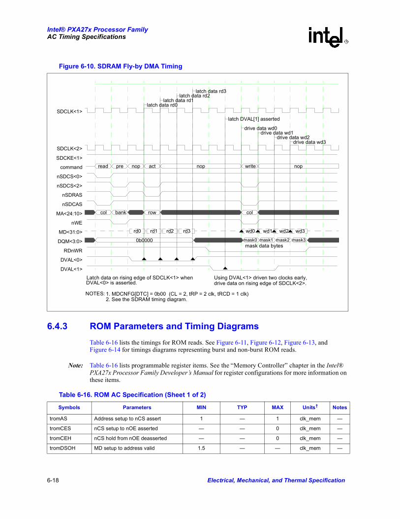
6-18 Electrical, Mechanical, and Thermal Specification
Intel® PXA27x Processor Family AC Timing Specifications
6.4.3 ROM Parameters and Timing Diagrams
Table 6-16 lists the timings for ROM reads. See Figure 6-11, Figure 6-12, Figure 6-13, and Figure 6-14 for timings diagrams representing burst and non-burst ROM reads.
Note: Table 6-16 lists programmable register items. See the “Memory Controller” chapter in the Intel® PXA27x Processor Family Developer’s Manual for register configurations for more information on these items.
Figure 6-10. SDRAM Fly-by DMA Timing
read pre nop act nop write nop
col bank row col
rd0 rd1 rd2 rd3 wd0 wd1 wd2 wd3
0b0000 mask0 mask1 mask2 mask3
drive data wd3drive data wd2
drive data wd1drive data wd0
latch DVAL[1] asserted
latch data rd3latch data rd2
latch data rd1latch data rd0
1. MDCNFG[DTC] = 0b00 (CL = 2, tRP = 2 clk, tRCD = 1 clk)
mask data bytes
Latch data on rising edge of SDCLK<1> whenDVAL<0> is asserted.
Using DVAL<1> driven two clocks early,drive data on rising edge of SDCLK<2>.
SDCLK<1>
SDCLK<2>
SDCKE<1>
command
nSDCS<0>
nSDCS<2>
nSDRAS
nSDCAS
MA<24:10>
nWE
MD<31:0>
DQM<3:0>
RDnWR
DVAL<0>
DVAL<1>
2. See the SDRAM timing diagram.NOTES:
Table 6-16. ROM AC Specification (Sheet 1 of 2)
Symbols Parameters MIN TYP MAX Units† Notes
tromAS Address setup to nCS assert 1 — 1 clk_mem —
tromCES nCS setup to nOE asserted — — 0 clk_mem —
tromCEH nCS hold from nOE deasserted — — 0 clk_mem —
tromDSOH MD setup to address valid 1.5 — — clk_mem —

Electrical, Mechanical, and Thermal Specification 6-19
Intel® PXA27x Processor FamilyAC Timing Specifications
tromDOH MD hold from address valid 0 — — clk_mem —
tromAVDVFAddress valid to data valid for the first read access
2 MSCx[RDF]+2 32 clk_mem —
tromAVDVSAddress valid to data valid for subsequent reads of non-burst devices
1 MSCx[RDF]+1 31 clk_mem —
tflashAVDVSAddress valid to data valid for subsequent reads of burst devices
1 MSCx[RDN]+1 31 clk_mem —
tromCDnCS deasserted after a read of next nCS or nSDCS asserted (minimum)
1MSCx[RRR]*2+
115 clk_mem —
† Numbers shown as integer multiples of the clk_mem period are ideal. Actual numbers vary with pin-to-pin differences in loading and transition direction (rise or fall). For more information, refer to the “Memory Control” chapter in the Intel® PXA27x Processor Family Developer’s Manual.
Table 6-16. ROM AC Specification (Sheet 2 of 2)
Symbols Parameters MIN TYP MAX Units† Notes

6-20 Electrical, Mechanical, and Thermal Specification
Intel® PXA27x Processor Family AC Timing Specifications
Figure 6-11. 32-Bit Non-burst ROM, SRAM, or Flash Read Timing
0 1 2 3
0b00
0b00/0b01/0b10/0b11
0b00
corresponding mask value
tromCD
tromAVDVS
tromAVDVStromAVDVS
tromAVDVF
tromAS
tromDOHtromDSOH
tromDOHtromDSOH
tromDOHtromDSOH
tromDOHtromDSOH
tromCEHtromCES
NOTE: MSC0[RDF0] = 4, MSC0[RRR0] = 1
CLK_MEM
nCS<0>
MA<25:2>
MA<1:0>(SA1110x='0')
MA<1:0>(SA1110x='1')
nADV(nSDCAS)
nOE
nWE
RDnWR
MD<31:0>
DQM<3:0>(SA1110x='0')
DQM<3:0>(SA1110x='1')
nCSx or nSDCSx

Electrical, Mechanical, and Thermal Specification 6-21
Intel® PXA27x Processor FamilyAC Timing Specifications
Figure 6-12. 32-Bit Burst-of-Eight ROM or Flash Read Timing
0 1 2 3 4 5 6 7
0b00
0b00/0b01/0b10/0b11
0b0000
corresponding mask value
tromCD
tromAVDVStromAVDVF
tDOHtDSOH
tCEHtCES
tAS
NOTE: MSC0[RDF0] = 4, MSC0[RDN0] = 1, MSC0[RRR0] = 1
CLK_MEM
nCS<0>
MA<25:5>
MA<4:2>
MA<1:0>(SA1110x='0')
MA<1:0>(SA1110x='1')
nADV(nSDCAS)
nOE
nWE
RDnWR
MD<31:0>
DQM<3:0>(SA1110x='0')
DQM<3:0>(SA1110x='1')
nCSx or nSDCSx

6-22 Electrical, Mechanical, and Thermal Specification
Intel® PXA27x Processor Family AC Timing Specifications
Figure 6-13. Eight-Beat Burst Read from 16-Bit Burst-of-Four ROM or Flash Timing
address
0 1 2 3 0 1 2 3
0b0
0b0/0b1
0b00
0b00 or 0b10/0b01
tromCD
tromAVDVS
tromAVDVFtromAVDVS
tromAVDVF
tromDOHtromDSOH
tromDOHtromDSOH
tromCEHtromCES
tromAS
NOTE: MSC0[RDF0] = 4, MSC0[RDN0] = 1, MSC0[RRR0] = 0
CLK_MEM
nCS<0>
MA<25:4>
MA<3>
MA<2:1>
MA<0>(SA1110x='0')
MA<0>(SA1110x='1')
nADV(nSDCAS)
nOE
nWE
RDnWR
MD<15:0>
DQM<1:0>(SA1110x='0')
DQM<1:0>(SA1110x='1')
nCSx or nSDCSx

Electrical, Mechanical, and Thermal Specification 6-23
Intel® PXA27x Processor FamilyAC Timing Specifications
6.4.4 Flash Memory Parameters and Timing Diagrams
The following sections describe the read/write parameters and timing diagrams for asynchronous and synchronous flash-memory interfaces with the memory controller.
6.4.4.1 Flash Memory Read Parameters and Timing Diagrams
Section 6.4.4.1.1 describes asynchronous flash reads. Section 6.4.4.1.2 describes synchronous flash reads.
6.4.4.1.1 Asynchronous Flash Read Parameters and Timing Diagrams
The timings listed in Table 6-16 for ROM reads also apply to asynchronous flash reads. See Figure 6-11, Figure 6-12, Figure 6-13, and Figure 6-14 for timings diagrams representative of an asynchronous flash read.
Figure 6-14. 16-bit ROM/Flash/SRAM Read for 4/2/1 Bytes Timing
addr addr + 1 addr addr addr addr + 1
0 0 0 0
0/1 0/1 0/1 0/1
0b00 0b00 0b00 0b00
mask mask mask mask
tflashAVDVS
tromAVDVFtromAVDVFtromAVDVFtromAVDVS
tromAVDVF
tromCDtromCD
tromCD
tromDOH
tromDSOHtromDOH
tromDSOH
tromDOHtromDSOH
tromDOHtromDSOH
tromDOH
tromDSOH
tromDOH
tromDSOH
tromCEStromCES
tromCEStromCEH
tromCES
tromAStromAS
tromAStromAS
32-bit read
NOTE: MSC0[RDF0] = 2, MSC0[RDN0] = 1, MSC0[RRR0] = 1
16-bit read 8-bit read
Applies to:16-bit ROM or
non-burst flash16-bit SRAM
Applies to:16-bit ROM or
non-burst flash16-bit SRAM16-bit burst flash
Applies to:16-bit ROM or
non-burst flash16-bit SRAM16-bit burst flash
32-bit Read
Applies to:16-bit Burst Flash
CLK_MEM
nCS<0>
MA<25:1>
MA<0>(SA1110x='0')
MA<0>(SA1110x='1')
nADV(nSDCAS)
nOE
nWE
RDnWR
MD<15:0>
DQM<1:0>(SA1110x='0')
DQM<1:0>(SA1110x='1')

6-24 Electrical, Mechanical, and Thermal Specification
Intel® PXA27x Processor Family AC Timing Specifications
6.4.4.1.2 Synchronous Flash Read Parameters and Timing Diagrams
Table 6-17 lists the timing parameters used in Figure 6-15, and, for flash packages, Figure 6-16.
Table 6-17. Synchronous Flash Read AC Specifications (Sheet 1 of 2)
Symbols Parameters MIN TYP MAX MIN TYP MAX MIN TYP MAX Units
No
tes
Divide by 12 Divide by 23 Divide by 44
tffCLK SDCLK0 period 9.6 — 38.519.2
— 76.9 38.5 — 154 ns 1
tffASMA<25:0> setup to nSDCAS (as nADV) asserted
1 — 1 1 — 2 1 — 4 CLK_MEM —
tffCESnCS setup to nSDCAS (as nADV) asserted
1 — 1 1 — 2 1 — 4 CLK_MEM —
tffADVnSDCAS (as nADV) pulse width
1 — 1 3 — 3 7 — 7 CLK_MEM —
tffOSnSDCAS (as nADV) de-assertion to nOE assertion
1
FCC – 1 (for
FCC<5)
FCC – 2
(for FCC>=5)
13 2
(FCC – 1)* 2(for
FCC<5)
(FCC – 2)* 2(for
FCC>=5)
26 7
(FCC * 4) – 7(for
FCC<5)
(FCC – 2) * 4(for
FCC>=5)
52 CLK_MEM 5
tffCEHnOE de-assertion to nCS de-assertion
4 — 4 8 — 8 16 — 16 CLK_MEM —
tffDS CLK to data valid 2 FCC 15 2 FCC 15 2 FCC 15 CLK_MEM 5
VCC_MEM = 1.8V +20%/-5%6
VCC_MEM = 2.5V +/- 10%7
VCC_MEM = 3.3V +/- 10%8
tffSDOS
MA<25:0>, MD<31:0>, DQM<3:0>, nCS<3:0>, nSDCAS (nADV), nWE, nOE, RDnWR output setup time to SDCLK<2:1> rise
TBD — —TBD
— — TBD — — ns —
tffSDOH
MA<25:0>, MD<31:0>, DQM<3:0>, nCS<3:0>, nSDCAS (nADV), nWE, nOE, RDnWR output hold time from SDCLK<2:1> rise
TBD — —TBD
— — TBD — — ns —
VCC_CORE = 0.85 V +/– 10%, with 1.71 V<= VCC_MEM <= 3.63 V
VCC_CORE = 1.1 V +/– 10%, with 1.71 V <= VCC_MEM <= 3.63 V
VCC_CORE = 1.3 V +/– 10%, with 1.71 V <= VCC_MEM <= 3.63 V

Electrical, Mechanical, and Thermal Specification 6-25
Intel® PXA27x Processor FamilyAC Timing Specifications
tffSDIS
MD<31:0> read data input setup time from SDCLK<2:0> rise
TBD — — 0.5 — — 0.5 — — ns —
tffSDIH
MD<31:0> read data input hold time from SDCLK<2:0> rise
TBD — — 1.8 — — 1.8 — — ns —
NOTES:1. SDCLK0 may be configured to be CLK_MEM divided by 1, 2 or 4. SDCLK0 for synchronous flash memory can be at the slowest,
divide-by-4 of the 26-MHz CLK_MEM. The fastest possible SDCLK0 is accomplished by configuring CLK_MEM at 104 MHz and clearing the MDREFR[K0DB2] or MDREFR[K0DB4] bit fields.
2. SDCLK0 frequency equals CLK_MEM frequency (MDREFR[K0DB4] and MDREFR[K0DB2] bit fields are clear)3. SDCLK0 frequency equals CLK_MEM/2 frequency (MDREFR[K0DB2] is set and MDREFR[K0DB4] is clear).4. SDCLK0 frequency equals CLK_MEM/4 frequency (MDREFR[K0DB4] is set).5. Use SXCNFG[SXCLx] to configure the value for the frequency configuration code (FCC).6. These numbers are for VCC_MEM = 1.8 V +20%/-5%, VOL = 0.4 V, and VOH = 1.4 V, with each applicable 4-bit field of the system
memory buffer strength registers (BSCN TRP and BSCNTRN) set to TBD (msb:lsb) and each applicable SDCLK0 divide-by-2 and divide-by-4 register bits (MDREFR[K0DB2] and MDREFR[K0DB4]) clear. If MDREFR[K0DB2 is set, the corresponding output setup and hold times are increased and decreased, respectively, by 0.25 times the SDCLK0 period.
7. These numbers are for VCC_MEM = 2.5 V +/– 10%, VOL = 0.4 V, and VOH = 2.1 V, with each applicable 4-bit field of the system memory buffer strength registers (BSCNTRP and BSCNTRN) set to 0b1010 (msb:lsb) and each applicable SDCLK0 divide-by-2 and divide-by-4 register bit (MDREFR[K0DB2] and MDREFR[K0DB4]) clear. If MDREFR[K0DB2 is set, the corresponding output setup and hold times are increased and decreased, respectively, by 0.25 times the SDCLK0 period.
8. These numbers are for VCC_MEM = 3.3 V +/– 10%, VOL = 0.4 V, and VOH = 2.4 V, with each applicable 4-bit field of the system memory buffer strength registers (BSCNTRP and BSCNTRN) set to 0b1010 (msb:lsb) and each applicable SDCLK0 divide-by-2 and divide-by-4 register bit (MDREFR[K0DB2] and MDREFR[K0DB4]) clear. If MDREFR[K0DB2 is set, the corresponding output setup and hold times are increased and decreased, respectively, by 0.25 times the SDCLK0 period.
Table 6-17. Synchronous Flash Read AC Specifications (Sheet 2 of 2)
Symbols Parameters MIN TYP MAX MIN TYP MAX MIN TYP MAX Units
No
tes

6-26 Electrical, Mechanical, and Thermal Specification
Intel® PXA27x Processor Family AC Timing Specifications
Figure 6-15. Synchronous Flash Burst-of-Eight Read Timing
0b00
0b00/0b01/0b10/0b11
0b0000
corresponding mask value
CODE+1
CODE
NOTES: 1) SXCNFG[CL] = 0b100 (CL = 5, frequency code configuration = 4) 2) CODE = frequency configuration code
CLK_MEM
SDCLK<0>
MA<19:2>
MA<1:0>(SA1110x=0)
MA<1:0>(SA1110x=1)
nCS<0>
nADV(nSDCAS)
nOE
nWE
MD<31:0>
DQM<3:0>(SA1110x=0)
DQM<3:0>(SA1110x=1)

Electrical, Mechanical, and Thermal Specification 6-27
Intel® PXA27x Processor FamilyAC Timing Specifications
Figure 6-16. Synchronous Flash Stacked Burst-of-Eight Read Timing
0b00
0b00/0b01/0b10/0b11
0b0000
corresponding mask value
CODE+1
CODE
NOTE: SXCNFG[CL] = 0b100 (CL = 5, frequency code configuration = 4) SA1110CR[SXSTACK] = 0b01
CLK_MEM
SDCLK<3>
MA<19:2>
MA<1:0>(SA1110x=0)
MA<1:0>(SA1110x=1)
nCS<0>
nADV(nSDCAS)
nOE
nWE
MD<31:0>
DQM<3:0>(SA1110x=0)
DQM<3:0>(SA1110x=1)

6-28 Electrical, Mechanical, and Thermal Specification
Intel® PXA27x Processor Family AC Timing Specifications
Figure 6-17 indicates which clock data would be latched following the assertion of nSDCAS(ADV), depending on the configuration of the SXCNFG[SXCLx] bit field. The period in the diagram indicated by different frequency-configuration codes (Fcodes or FCCs) is equal to the number of SDCLK0 cycles between the READ command and the clock edge on which data is driven onto the bus.
Figure 6-17. First-Access Latency Configuration Timing
Valid Address
0b0000
Beat 0 Beat 1 Beat 2 Beat 3 Beat 4 Beat 5
Beat 0 Beat 1 Beat 2 Beat 3 Beat 4
Beat 0 Beat 1 Beat 2 Beat 3
Beat 0 Beat 1 Beat 2
Beat 0 Beat 1
Beat 0
Code 7
Code 6
Code 5
Code 4
Code 3
Code 2
NOTE: CODE = Frequency Configuration Code
SDCLK<0>
nCS<0>
MA<19:0>
nSDCAS
DQM<3:0>
MD (Code = 2)
MD (Code = 3)
MD (Code = 4)
MD (Code = 5)
MD (Code = 6)
MD (Code = 7)

Electrical, Mechanical, and Thermal Specification 6-29
Intel® PXA27x Processor FamilyAC Timing Specifications
The burst-read example shown in Figure 6-18 represents waveforms that result when SXCNFG[SXCLx] is configured as 0b0100, representing a frequency-configuration code equal to 3. The following example can be used to help determine the appropriate setting for SXCNFG[SXCLx].
Parameters defined by the processor:
• tffSDOH (max) = SDCLK<0> to CE# (nCE), ADV# (nADV), or address valid, whichever occurs last
• tffSDIS (min) = Data setup to SDCLK<0>
Parameters defined by flash memory:
• tVLQV (min) = ADV# low to output delay
• tVLCH (min) = ADV# low to clock
• tCHQV (max) = SDCLK<0> to output valid
Use the following equations when calculating the frequency configuration code:(1) SDCLK period = (1/frequency)
(2) n (SDCLK period) ≥ tVLQV - tVLCH - tCHQV(3) n = (tVLQV - tVLCH - tCHQV)/SDCLK period, where
n = frequency configuration code rounded up to integer value
(4) SDCLK period ≥ tCHQV + tffSDIS
Example
The timing information below is only an example. See Table 6-17 for actual synchronous AC timings.
SDCLK<0> frequency = 50 MHz
tVLQV = 70 ns (typical timing from synchronous flash memory)
tVLCH = 10 ns (min)
tCHQV = 14 ns (min)
From Eq.(1): 1/50 (MHz) = 20 ns
From Eq.(2): n(20 ns) ≥ 70 ns - 10 ns - 14 nsn(20 ns) ≥ 46 nsn = (46/20) ns = 2.3 ns
n = 3
Use equation 4 to help verify the maximum possible frequency at which the synchronous flash memory can run with the memory controller. The following example uses equation 4:
SDCLK<0> frequency = 66 MHz
tCHQV = 11 ns (max)
tffSDIS = 3 ns (min)
From Eq. (1): 1/66 (MHz) = 15.15 ns
From Eq. (4): 15.15 ns ≥ 11 ns + 3 ns15.15 ns ≥ 14 ns
The results from this example indicate that the 66-MHz memory works without problems with the memory controller.
Note: All AC timings must be considered to avoid timing violations in the memory-to-memory-controller interface.

6-30 Electrical, Mechanical, and Thermal Specification
Intel® PXA27x Processor Family AC Timing Specifications
6.4.4.2 Flash Memory Write Parameters and Timing Diagrams
Table 6-18 lists the AC specification for both burst and non-burst flash writes shown in Figure 6-19 and, for stacked flash packages, Figure 6-20.
Figure 6-18. Synchronous Flash Burst Read Example
Valid Address
Beat 0 Beat1
tCHQV
tffSDOH
tffSDOH
tffSDOH
tffSDIS
tVLQV
tAVCH
SDCLK<0>
nCS<0>
nSDCAS (ADV#)
MA
MD
Table 6-18. Flash Memory AC Specification (Sheet 1 of 2)
Symbols Parameters MIN TYP MAX Units1 Notes
tflashAS Address setup to nCS assert 1 — 1 clk_mem —
tflashAH Address hold from nWE de-asserted 1 — 1 clk_mem —
tflashASW Address setup to nWE asserted 1 — 3 clk_mem 2
tflashCES nCS setup to nWE asserted 2 — 2 clk_mem —
tflashCEH nCS hold from nWE de-asserted 1 — 1 clk_mem —
tflashWL nWE asserted time 1 MSCx[RDF]+1 31 clk_mem —
tflashDSWH MD/DQM setup to nWE de-asserted 2 MSCx[RDF]+2 32 clk_mem —
tflashDHMD/DQM hold from nWE de-asserted
1 — 1 clk_mem —
tflashDSOH MD setup to address valid 1.5 — — clk_mem —
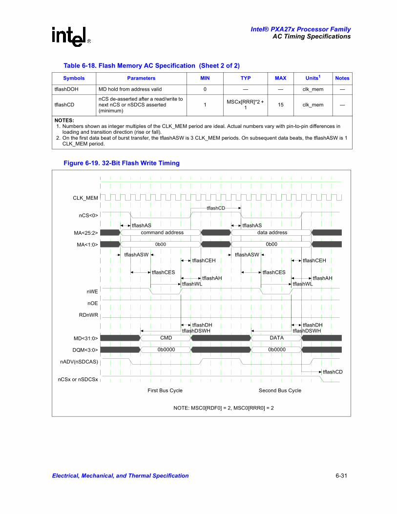
Electrical, Mechanical, and Thermal Specification 6-31
Intel® PXA27x Processor FamilyAC Timing Specifications
tflashDOH MD hold from address valid 0 — — clk_mem —
tflashCDnCS de-asserted after a read/write to next nCS or nSDCS asserted (minimum)
1MSCx[RRR]*2 +
115 clk_mem —
NOTES:1. Numbers shown as integer multiples of the CLK_MEM period are ideal. Actual numbers vary with pin-to-pin differences in
loading and transition direction (rise or fall).2. On the first data beat of burst transfer, the tflashASW is 3 CLK_MEM periods. On subsequent data beats, the tflashASW is 1
CLK_MEM period.
Figure 6-19. 32-Bit Flash Write Timing
Table 6-18. Flash Memory AC Specification (Sheet 2 of 2)
Symbols Parameters MIN TYP MAX Units1 Notes
command address data address
0b00 0b00
CMD DATA
0b0000 0b0000
tflashCD
tflashDSWHtflashDSWH
tflashWLtflashWL
tflashCD
tflashDHtflashDH
tflashAH
tflashCEH
tflashCES
tflashASW
tflashAH
tflashCEH
tflashCES
tflashASW
tflashAStflashAS
NOTE: MSC0[RDF0] = 2, MSC0[RRR0] = 2
First Bus Cycle Second Bus Cycle
CLK_MEM
nCS<0>
MA<25:2>
MA<1:0>
nWE
nOE
RDnWR
MD<31:0>
DQM<3:0>
nADV(nSDCAS)
nCSx or nSDCSx

6-32 Electrical, Mechanical, and Thermal Specification
Intel® PXA27x Processor Family AC Timing Specifications
Figure 6-20. 32-Bit Stacked Flash Write Timing
command address data address
0b00 0b00
CMD DATA
0b0000 0b0000
tflashCD
tflashDSWHtflashDSWH
tflashWLtflashWL
tflashCD
tflashDHtflashDH
tflashAH
tflashCEH
tflashCES
tflashASW
tflashAH
tflashCEH
tflashCES
tflashASW
tflashAStflashAS
* MSC0[RDF0] = 2, MSC0[RRR0] = 2, SA1110SXSTACK] = 00
First Bus Cycle Second Bus Cycle
CLK_MEM
nWE
MA<25:2>
MA<1:0>
nCS<0> or nCS<1>
nOE
RDnWR
MD<31:0>
DQM<3:0>
nADV(nSDCAS)
nCSx

Electrical, Mechanical, and Thermal Specification 6-33
Intel® PXA27x Processor FamilyAC Timing Specifications
6.4.5 SRAM Parameters and Timing Diagrams
The following sections describe the read/write parameters and timing diagrams for SRAM interfaces with the memory controller.
6.4.5.1 SRAM Read Parameters and Timing Diagrams
The timing for a read access is identical to that for a non-burst ROM read (see Figure 6-11). The timings listed in Table 6-16 for ROM reads are also used for SRAM reads. See Figure 6-11 and Figure 6-14 for timings diagrams representing 16-bit SRAM transferring four, two, and one byte(s) during read-bus tenures.
6.4.5.2 SRAM Write Parameters and Timing Diagrams
Figure 6-22 and Figure 6-23 show the timing for 32-bit and 16-bit SRAM writes. Table 6-19 lists the timings used in Figure 6-22 and Figure 6-23.
Figure 6-21. 16-Bit Flash Write Timing
addr
0b0
Bytes 1:0
0b00
tflashCD
tflashDSWH
tflashWL
tflashDH
tflashCEH
tflashCES
tflashAS
Applies to:16-bit Non-Burst Flash16-bit Burst Flash
NOTE: MSC1[RDN2] = 2, MSC1[RDF2] = 1, MSC1[RRR2] = 2
CLK_MEM
nCS<2>
MA<25:1>
MA<0>
nWE
nOE
RDnWR
MD<15:0>
DQM<1:0>
nADV(nSDCAS)
nCSx or nSDCSx

6-34 Electrical, Mechanical, and Thermal Specification
Intel® PXA27x Processor Family AC Timing Specifications
During writes, data pins are actively driven by the processor and are not three-stated, regardless of the states of the individual DQM signals. For SRAM writes, the DQM signals are used as byte enables.
Note: Table 6-19 lists programmable register items. See the “Memory Controller”chapter in the Intel® PXA27x Processor Family Developer’s Manual for register configurations for more information on these items.
Table 6-19. SRAM Write AC Specification
Symbols Parameters MIN TYP MAX Units1 Notes
tsramAS Address setup to nCS assert 1 — 1 clk_mem —
tsramAH Address hold from nWE de-asserted 1 — 1 clk_mem —
tsramASW Address setup to nWE asserted 1 — 3 clk_mem 2
tsramCES nCS setup to nWE asserted 2 — 2 clk_mem —
tsramCEH nCS hold from nWE de-asserted 1 — 1 clk_mem —
tsramWL nWE asserted time 1 MSCx[RDN]+1 31 clk_mem —
tsramDSWH MD/DQM setup to nWE de-asserted 2 MSCx[RDN]+2 32 clk_mem —
tsramDHMD/DQM hold from nWE de-asserted
1 — 1 clk_mem —
tramCDnCS de-asserted after a read to next nCS or nSDCS asserted (minimum)
1MSCx[RRR]*2+
115 clk_mem —
NOTES:1. Numbers shown as integer multiples of the CLK_MEM period are ideal. Actual numbers vary with pin-to-pin differences in
loading and transition direction (rise or fall).2. On the first data beat of burst transfer, the tsramASW is 3 CLK_MEM periods. On subsequent data beats, the tsramASW is 1
CLK_MEM period.
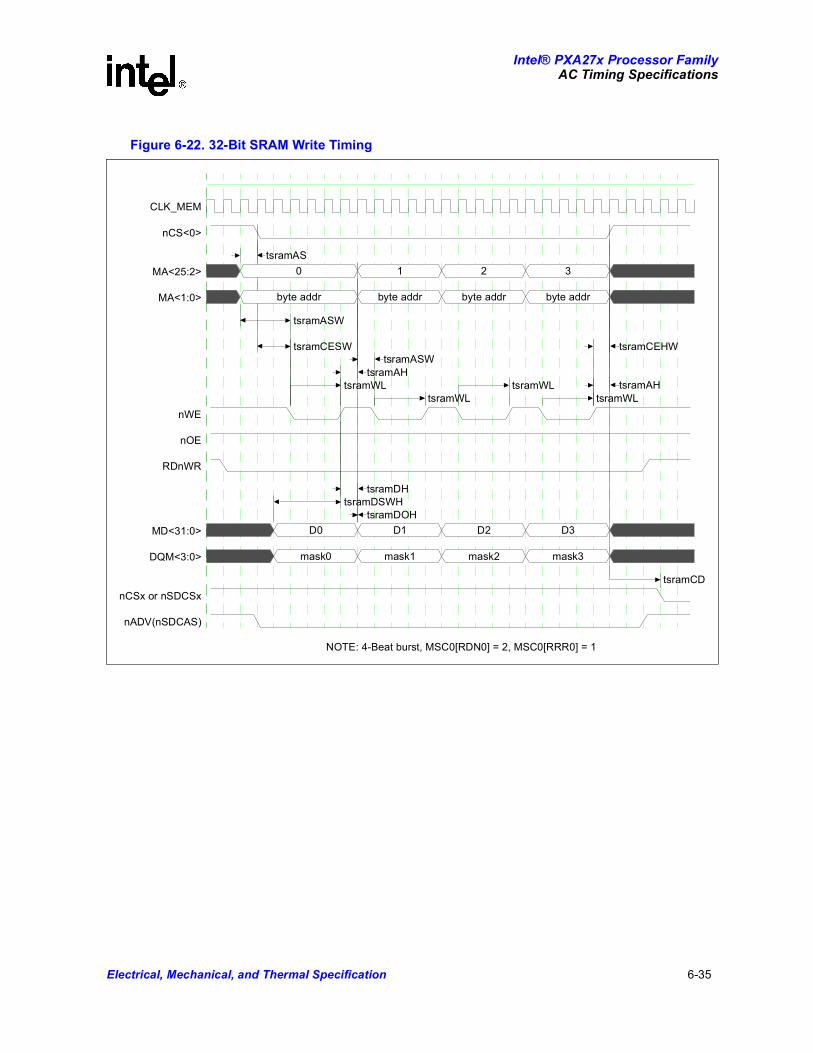
Electrical, Mechanical, and Thermal Specification 6-35
Intel® PXA27x Processor FamilyAC Timing Specifications
Figure 6-22. 32-Bit SRAM Write Timing
0 1 2 3
byte addr byte addr byte addr byte addr
D0 D1 D2 D3
mask0 mask1 mask2 mask3
tsramCD
tsramWLtsramWL
tsramWLtsramWL
tsramDOH
tsramDHtsramDSWH
tsramCEHW
tsramAH
tsramASWtsramAH
tsramASW
tsramCESW
tsramAS
NOTE: 4-Beat burst, MSC0[RDN0] = 2, MSC0[RRR0] = 1
CLK_MEM
nCS<0>
MA<25:2>
MA<1:0>
nWE
nOE
RDnWR
MD<31:0>
DQM<3:0>
nCSx or nSDCSx
nADV(nSDCAS)

6-36 Electrical, Mechanical, and Thermal Specification
Intel® PXA27x Processor Family AC Timing Specifications
6.4.6 Variable-Latency I/O Parameters and Timing Diagrams
The following sections describe the read/write parameters and timing diagrams for VLIO memory interfaces with the memory controller.
Table 6-20 lists the timing-information references for both the read and the write timing diagrams.
Note: Table 6-20 lists programmable register items. For more information on these items, see the “Memory Controller” chapter in the Intel® PXA27x Processor Family Developer’s Manual for register configurations.
Figure 6-23. 16-bit SRAM Write for 4/2/1 Byte(s) Timing
addr addr+1 addr addr
'0' '0' '0' '0' or '1'
Bytes 1:0 Bytes 3:2 Bytes 1:0 Byte 0 OR 1
0b00 0b00 0b01/0b10
tsramCD
tsramDSWH
tsramDSWH
tsramDSWH
tsramWLtsramWLtsramWLtsramWL
tsramCDtsramCD
tsramDHtsramDH
tsramDSWH
tsramDH
tsramDH
tsramCEH
tsramCES
tsramCEH
tsramCEStsramCEH
tsramWLtsramASW
tsramAHtsramCES
tramAStramAStramAS
32-bit Write 16-bit Write 8-bit Write
NOTE: MSC1[RDF2]=1, MSC1[RDN]=2, MSC1[RRR2]=2
CLK_MEM
nCS<2>
MA<25:1>
MA<0>
nWE
nOE
RDnWR
MD<15:0>
DQM<1:0>
nADV(nSDCAS)
nCSx or nSDCSx

Electrical, Mechanical, and Thermal Specification 6-37
Intel® PXA27x Processor FamilyAC Timing Specifications
6.4.6.1 Variable Latency I/O Read Timing
Figure 6-24 shows the timing for 32-bit variable-latency I/O (VLIO) memory reads. Table 6-20 lists the timing parameters used in these diagrams.
Table 6-20. VLIO Timing
Symbols Parameters MIN TYP MAX2 Units1 Notes
tvlioAS Address setup to nCS asserted 1 — 1 clk_mem —
tvlioAHAddress hold from nPWE/nOE de-asserted
2 MSCx[RDN] 30 clk_mem —
tvlioASRW0Address setup to nPWE/nOE asserted (1st access)
3 — 3 clk_mem —
tvlioASRWnAddress setup to nPWE/nOE asserted (next access(es))
2 MSCx[RDN] 30 clk_mem —
tvlioCES nCS setup to nPWE/nOE asserted 2 — 2 clk_mem —
tvlioCEHnCS hold from nPWE/nOE de-asserted
1 — 1 clk_mem —
tvlioDSWHMD/DQM setup (minimum) to nPWE de-asserted
5 MSCx[RDF]+2 32 clk_mem —
tvlioDHMD/DQM hold from nPWE de-asserted
1 — 1 clk_mem —
tvlioDSOH MD setup to address changing 1.5 — clk_mem —
tvlioDOH MD hold from address changing 0 — ns —
tvlioRDYHRDY hold from nPWE/nOE de-asserted
0 — — ns —
tvlioRWAnPWE/nOE assert period between writes
4MSC[RDF]+1 +
Waits31 + Waits
clk_mem —
tvlioRWDnPWE/nOE de-asserted period between writes
4 MSCx[RDN*2] 60 clk_mem 3
tvlioCDnCS de-asserted after a read/write to next nCS or nSDCS asserted (minimum)
1MSCx[RRR]*2 +
115 clk_mem —
NOTES:1. Numbers shown as integer multiples of the CLK_MEM period are ideal. Actual numbers vary with pin-to-pin differences in
loading and transition direction (rise or fall).2. Maximum values reflect the register dynamic ranges.3. Depending on the programmed value of MSC[RDN] and the clk_mem speed, this can be a significant amount of time.
Bulverde does not drive the data bus during this time between transfers. If the VLIO does not drive the data bus during this time between transfers, the data bus is not driven for this period of time. If MSC[RDN] is programmed to 60 (which equals 60 CLK_MEM cycles), then the data bus could potentially not be driven for 30*2 = 60 CLK_MEM cycles.

6-38 Electrical, Mechanical, and Thermal Specification
Intel® PXA27x Processor Family AC Timing Specifications
6.4.6.2 Variable-Latency I/O Write Timing
Figure 6-25 shows the timing for 32-bit VLIO memory writes. Table 6-20 list the timing parameters used in Figure 6-25.
Figure 6-24. 32-Bit VLIO Read Timing
addr addr + 1 addr + 2 addr + 3
0b00
0b00/0b01/0b10/0b11
0b0000
corresponding mask value
tvlioCD
tvlioRWAtvlioRWDtvlioRWA
tvlioRWDtvlioRWA
tvlioRWD
tvlioDOHtvlioDSOH
tvlioDOHtvlioDSOH
tvlioDOHtvlioDSOH
tvlioDOHtvlioDSOH
tvlioRDYHtvlioRDYHtvlioRDYH
tvlioRDYH
tvlioCEH
tvlioAHtvlioASRWn
tvlioAH
tvlioASRWn
tvlioAH
tvlioASRWn
tvlioAHtvlioASRW0
tvlioCES
tvlioAS
0 Waits 1 Wait 2 Waits 3 Waits
NOTE: MSC0[RDF0] = 3, MSC0[RDN0 = 2, MSC0[RRR0] = 1
CLK_MEM
nCS<0>
MA<25:2>
MA<1:0>(SA1110x='0')
MA<1:0>(SA1110x='1')
nOE
nPWE
RDnWR
RDY
RDY_sync
MD<31:0>
DQM<3:0>(SA1110x='0')
DQM<3:0>(SA1110x='1')
nCSx or nSDCSx

Electrical, Mechanical, and Thermal Specification 6-39
Intel® PXA27x Processor FamilyAC Timing Specifications
Figure 6-25. 32-Bit VLIO Write Timing
addr addr + 1 addr + 2 addr + 3
0b00
D0 D1 D2 D3
mask0 mask1 mask2 mask3
tvlioCD
tvlioRWAtvlioRWD
tvlioRWA
tvlioRWDtvlioRWA
tvlioRWD
tvlioRWA
tvlioDHtvlioDH
tvlioDSWH
tvlioDH
tvlioDSWH
tvlioDHtvlioDSWH
tvlioDSWH
tvlioRDYHtvlioRDYHtvlioRDYH
tvlioRDYH
tvlioCEH
tvlioAHtvlioASRWn
tvlioAH
tvlioASRWn
tvlioAH
tvlioASRWn
tvlioAH
tvlioASRW0
tvlioCES
tvlioAS
0 Waits
NOTE: MSC0[RDF0] = 3, MSC0[RDN0] = 2, MSC0[RRR0] = 1
1 Wait 2 Waits 3 Waits
CLK_MEM
nCS<0>
MA<25:2>
MA<1:0>
nPWE
nOE
RDnWR
RDY
RDY_sync
MD<31:0>
DQM<3:0>
nCSx or nSDCSx

6-40 Electrical, Mechanical, and Thermal Specification
Intel® PXA27x Processor Family AC Timing Specifications
6.4.7 Expansion-Card Interface Parameters and Timing Diagrams
The following sections describe the read/write parameters and timing diagrams for CompactFlash* and PC Card* (expansion card) memory interfaces with the memory controller.
Table 6-21 shows the timing parameters used in the timing diagrams, Figure 6-26 and Figure 6-27.
Note: Table 6-21 lists programmable register items. See the “Memory Controller” chapter in the Intel® PXA27x Processor Family Developer’s Manual for register configurations for more information on these items.
Table 6-21. Expansion-Card Interface AC Specifications
Symbols Parameters MIN TYP MAX Units Notes
tcdAVCL Address Valid to CMD Low 2 MCx[SET] 127 CLK_MEM 1,2,3,4
tcdCHAI CMD High to Address Invalid 0 MCx[HOLD] 63 CLK_MEM 1,2,3,5
tcdDVCL Write Data Valid to CMD Low — 1 — CLK_MEM 1,3
tcdCHWDI CMD High to Write Data Invalid — 4 — CLK_MEM 1,3
tcdDVCH Read Data Valid to CMD High 2 — — CLK_MEM 1,3
tcdCHRDI CMD High to Read Data Invalid 0 — — ns 3
tcdCMD CMD Assert During Transfers —
tcdCLPS + tcdPHCH +
nPWAIT assertion
— CLK_MEM 1,3
tcdILCL nIOIS16 Low to CMD Low 4 — — CLK_MEM 1,3
tcdCHIH CMD High to nIOIS16 High 2 — — CLK_MEM 1,3
tcdCLPS CMD Low to nPWAIT Sample — x_ASST_WAIT — CLK_MEM 1,3,6,7
tcdPHCH nPWAIT High to CMD High — x_ASST_HOLD — CLK_MEM 1,3,6,8
NOTES:1. All numbers shown are ideal, integer multiples of the CLK_MEM period. Actual numbers vary with pin-to-pin differences in
loading and transition direction (rise or fall). 2. Includes signals MA[25:0], nPREG, and nPSKTSEL.3. CMD refers to signals nPWE, nPOE, nPIOW, and nPIOR4. Refer to the Intel® PXA27x Processor Family Developer’s Manual, Expansion Memory Timing Configuration registers to
change the assertion of CMD using the MCx[SET] bit fields.5. Refer to the Intel® PXA27x Processor Family Developer’s Manual, Expansion Memory Timing Configuration registers to
increase the assertion of CMD using the MCx[HOLD] bit fields.6. Refer to the Intel® PXA27x Processor Family Developer’s Manual, Expansion Memory Timing Configuration registers to
increase timings. The timings are changed by programming the MCx[ASST] respective bit fields. Refer to the PC Card Interface Command Assertion Code table to see the effect of MCx[ASST].
7. tcdCLPS equals CLK_MEM * x_ASST_WAIT. Refer to the PC Card Interface Command Assertion Code table in the Intel® PXA27x Processor Family Developer’s Manual for the correlation between x_ASST_WAIT and the MCx[ASST] bit field.
8. tcdPHCH equals CLK_MEM * x_ASST_HOLD. Refer to the PC Card Interface Command Assertion Code table in the Intel® PXA27x Processor Family Developer’s Manual for the correlation between x_ASST_HOLD and the MCx[ASST] bit field.

Electrical, Mechanical, and Thermal Specification 6-41
Intel® PXA27x Processor FamilyAC Timing Specifications
Figure 6-26. Expansion-Card Memory or I/O 16-Bit Access Timing
Read Data Latch
tcdCMD
tcdPHCH
tcdCLPS
tcdAVCL
tcdCHAI
tcdCHRDI
tcdDVCH
tcdCHWDItcdDVCL
tcdCHIHtcdILCL
CLK_MEM
nPCE[2],nPCE[1]
MA[25:0],nPREG,PSKTSEL
nPWE,nPOE,nPIOW,nPIOR
nIOIS16
MD[15:0] (write)
RDnWR
nPWAIT
MD[15:0] (read)

6-42 Electrical, Mechanical, and Thermal Specification
Intel® PXA27x Processor Family AC Timing Specifications
Figure 6-27. Expansion-Card Memory or I/O 16-Bit Access to 8-Bit Device Timing
Low Byte High Byte
Read Data LatchRead Data Latch
tcdPHCH
tcdCLPS
tcdPHCH
tcdCLPS
tcdCMDtcdCHAI
tcdAVCL
tcdCMDtcdCHAI
tcdAVCL
tcdCHWDItcdCHWDI
tcdDVCL
tcdCHRDI
tcdDVCH
tcdCHRDI
tcdDVCH
tcdCHIHtcdILCL
CLK_MEM
MA<25:1>,nPREG,PSKTSEL
MA<0>
nPCE<2>
nPCE<1>
nPIOW (or) nPIOR
RDnWR
nIOIS16
nPWAIT
MD<7:0> (read)
MD<7:0> (write)

Electrical, Mechanical, and Thermal Specification 6-43
Intel® PXA27x Processor FamilyAC Timing Specifications
6.5 LCD Timing Specifications
Figure 6-28 describes the LCD timing parameters. The LCD pin timing specifications are referenced to the pixel clock (L_PCLK_WR). Table 6-22 gives the values for the parameters.
Figure 6-28. LCD Timing Definitions
Table 6-22. LCD Timing Specifications
Symbol Description Min Max Units Notes
TpclkdvL_PCLK_WR rise/fall to L_LDD<17:0> driven valid
— 14 ns 1
TpclklvL_PCLK_WR fall to L_LCLK_A0 driven valid
— 14 ns 2
TpclkfvL_PCLK_WR fall to L_FCLK_RD driven valid
— 14 ns 2
Tpclkbv L_PCLK_WR rise to L_BIAS driven valid — 14 ns 2
NOTES:1. The LCD data pins can be programmed to be driven on either the rising or falling edge of the pixel clock
(L_PCLK_WR).2. These LCD signals can toggle when L_PCLK_WR is not clocking (between frames). At this time, they are
clocked with the internal version of the pixel clock before it is driven out onto the L_PCLK_WR pin.
L_LDD[17:0](rise)
L_LDD[17:0](fall)
L_PCLK_WR
L_LCLK_A0
L_BIAS
L_FCLK_RD
Tpclkdv
Tpclklv
Tpclkfv
Tpclkbv
Tpclkdv

6-44 Electrical, Mechanical, and Thermal Specification
Intel® PXA27x Processor Family AC Timing Specifications
6.6 SSP Timing Specifications
Figure 6-29 describes the SSP timing parameters. The SSP pin timing specifications are referenced to SSPCLK. Table 6-23 gives the values for the parameters.
Note: In Figure 6-29, read the term “tSFMV” as “TSTXV.”
Figure 6-30. Timing Diagram for SSP Slave Mode Transmitting Data to an External Peripheral
Figure 6-29. SSP Master Mode Timing Definitions
Table 6-23. SSP Master Mode Timing Specifications
Symbol Description Min Max Units Notes
Tsfmv SSPSCLK rise to SSPSFRM driven valid 21 ns
Trxds SSPRXD valid to SSPSCLK fall (input setup) 11 ns
Trxdh SSPSCLK fall to SSPRXD invalid (input hold) 0 ns
Tsfmv SSPSCLK rise to SSPTXD valid 22 ns
SSPSCLK
SSPSFRM
SSPTXD
SSPRXD
Tsfmv
Tsfmv
Trxds Trxdh
PXA27x processor transmitting data
SSPSCLK(from Peripheral)
SSPTXD(from SSP)
PXA27x SSP (Slave Mode) transmitting data to external peripheral
SSPSFRM(from Peripheral)
tSCLK2TXD_output_delay
tSFRM2TXD_output_delay
PXA27x processor transmitting data
SSPSCLK(from Peripheral)
SSPTXD(from SSP)
PXA27x SSP (Slave Mode) transmitting data to external peripheral
SSPSFRM(from Peripheral)
tSCLK2TXD_output_delay
tSFRM2TXD_output_delay

Electrical, Mechanical, and Thermal Specification 6-45
Intel® PXA27x Processor FamilyAC Timing Specifications
Table 6-24. Timing Specification for SSP Slave Mode Transmitting Data to External Peripheral
Figure 6-31. Timing Diagram for SSP Slave Mode Receiving Data from External Peripheral
Table 6-25. Timing Specification for SSP Slave Mode Receiving Data from External Peripheral
6.7 JTAG Boundary Scan Timing Specifications
Table 6-26 shows the AC specifications for the JTAG boundary-scan test signals. Figure 6-32 shows the timing diagram.
Parameter Description Min Typ Max Units
tSFRM2TXD_output_delay Frame to TX Data Out 10.58 ns
tSCLK2TXD_output_delay Clock to Tx Data Out 10.52 ns
Parameter Description Min Typical Max Units
tSFRM_input_delay Frame to Rx Data Capture 5.21 ns
tSCLK_input_delay Clock to Rx Data Capture 5.04 ns
tRXD_input_delay Rx Data Setup to Capture 4.81 ns
PXA27 processor receiving data
SSPSCLK(from Peripheral)
SSPRXD(from Peripheral)
SSPSFRM(from Peripheral)
PXA27x SSP (Slave Mode receiving data from external peripheral
Data Capture
tSCLK_input_delay
tSFRM_input_delay
tRXD_input_delay
Data Capture
PXA27 processor receiving data
SSPSCLK(from Peripheral)
SSPRXD(from Peripheral)
SSPSFRM(from Peripheral)
PXA27x SSP (Slave Mode receiving data from external peripheral
Data Capture
tSCLK_input_delay
tSFRM_input_delay
tRXD_input_delay
Data Capture
Table 6-26. Boundary Scan Timing Specifications (Sheet 1 of 2)
Symbol Parameter Min Max Units Notes
TBSF TCK Frequency 0.0 33.33 MHz —
TBSCH TCK High Time 15.0 — ns Measured at 1.5 V
TBSCL TCK Low Time 15.0 — ns Measured at 1.5 V
TBSCR TCK Rise Time — 5.0 ns 0.8 V to 2.0 V
TBSCF TCK Fall Time — 5.0 ns 2.0 V to 0.8 V

6-46 Electrical, Mechanical, and Thermal Specification
Intel® PXA27x Processor Family AC Timing Specifications
§§
TBSIS1 Input Setup to TCK TDI, TMS 4.0 — ns —
TBSIH1 Input Hold from TCK TDI, TMS 6.0 — ns —
TBSIS2 Input Setup to TCK nTRST 25.0 — ns —
TBSIH2 Input Hold from TCK nTRST 3.0 — ns —
TnTRST Assertion time of nTRST 6 — ms —
TBSOV1 TDO Valid Delay 1.5 6.9 ns Relative to falling edge of TCK
TOF1 TDO Float Delay 1.1 5.4 ns Relative to falling edge of TCK
Figure 6-32. JTAG Boundary-Scan Timing
Table 6-26. Boundary Scan Timing Specifications (Sheet 2 of 2)
Symbol Parameter Min Max Units Notes
Captu
re-IR
Shift-IR Run-Test/Idle
TOF1
TBSOV1
TBSOV1
TBSOV1
TBSOV1
TBSOV1
TBSOV1
TBSOV1
TBSIH1
TBSIS1
TBSIH1
TBSIS1
TBSIH2TBSIS2
TBSCL
TBSCH
TBSF
TCK
nTRST
TMS
TDI
TDO
Controller State
Test-L
ogic-
Reset
Run-T
est/I
dle
Selec
t-DR-S
can
Select-
IR-S
can
Exit1-
IR
Updat
e-IR
Test-L
ogic-
Reset
TnTRST

Electrical, Mechanical, and Thermal Specification A-1
Intel® PXA27x Processor Family Programmer Enabling A
The Intel PXA27x processor family is a high-performance, low-power microprocessor now available with additional memory chips. One of the chips available within the family is the Intel StrataFlash® wireless memory (L18).
A.1 Introduction
This chapter describes how to prepare the PXA27x processor for flash memory programming, and how to reduce programming time in a factory environment.
The PXA27x processor can be enabled to program flash using one of two different methods. One method focuses on programming the PXA27x processor prior to assembly; the other focuses on waiting until after the PXA27x processor has been assembled before programming. Perhaps both methods might be suitable, depending on the design requirements. This chapter explains the trade-offs between different methods, thus helping reduce time in a factory environment and/or reducing cost of development.
The direct-access programming method requires minimum software development and takes less time to program the flash memory. Direct-access programming requires that all other memory devices along with the PXA27x processor be placed into high-z (by issuing a JTAG high-z instruction) while programming the Intel StrataFlash® wireless memory. All the power domains must be brought up to their required voltages to prevent damage to the part. All other memories are placed into high-z by applying power and ensuring the de-assertion of their chip-select signals.
The second method for programming flash within the PXA27x processor requires a greater amount of code development through the JTAG controller. It is a slower programming method but requires fewer pins. This method does not require any of the memory address, data, or control signals to be pinned out. Flash loader code is loaded into the PXA27x processor mini-instruction cache. The code is then executed and uses the PXA27x memory controller to program the flash and de-select the other memory devices that might be present within the SCSP. This method is referred to as JTAG flash programming. All the power domains on PXA27x processors must be brought up to their required voltages to prevent damage to the part. All input signals not used must be driven to prevent excessive current usage. Refer to the Intel® PXA27x Processor Design Guide “Debug Interface” chapter for JTAG- specific command information.
Table A-1 shows the comparison using either the direct-access programming method or the JTAG flash programming method.

A-2 Electrical, Mechanical, and Thermal Specification
Intel® PXA27x Processor Family Intel® PXA27x Processor Family Programmer Enabling
1
A.2 Device Configuration
The PXA27x processor uses a PXA27x processor die combined with either flash memory die or flash and SDRAM memory chips all packaged together. Currently available PXA27x processor configurations are as follows:
• 32 MBytes of Intel StrataFlash® memory and 32 MBytes of low-power SDRAM
• 64 MBytes of Intel StrataFlash® memory
• 32 MBytes of Intel StrataFlash® memory
A.3 Procedure to Prepare Intel® PXA27x Processor for Programming Flash
The following steps describe the procedure to prepare the PXA27x processor using either the direct- access programming method or the JTAG-flash programming method. To prepare for direct-access programming, the internal memories other than flash are de-selected by de-asserting the dedicated chip-select signals and the PXA27x processor must be placed into high-Z using high-Z JTAG command.
To prepare for JTAG flash programming, bring the PXA27x processor out of reset. It is responsible for controlling all the memory signals and receiving the data to program the flash devices through the JTAG controller.
A.3.1 Sequence Required for Direct-Access Programming
Follow the steps below to prepare the PXA27x processor for direct-access programming. Use the power-on timing specifications with respect to applying power to the required domains as documented in Section 6.2.1.
1. Drive all memory chip selects (other than flash) to their inactive state to guarantee the other memories are not contending with the flash signals (that is, XCS signal for SDRAM must be driven high).
Table A-1. Direct Access versus JTAG Flash Programming1
Methods
Maximum MB/s Flash
Programming Time (32-bit)
Maximum MB/s Flash
Programming Time (16-bit)
Total Signals Required to be Pinout of End User Product
Software Development Effort
Direct Access Programming 57.14 28.574 512 JTAG high-z Instruction
JTAG Flash Programming 4.1255 4.1255 53 JTAG Flash Programmer residing within the mini I-cache
1. Data rates are best case not accounting for any overhead (that is, running a checksum algorithm and downloading the flash loader into the PXA27x processor mini-instruction cache)
2. These signals (include address, data, control and JTAG) require a connector on the end user’s product. 3. Depending on the system design, a connector on the end user's product requires nRESET, nTRST, TMS, TDI, and TCK. TDO
is optional.4. Calculated based on TCK (max) = 33 MHz. MB/s = 33 HMz/8 bits5. Calculated based on tWLWH = 50ns and tWHWL = 20ns. MB/s = 1/((tWLWH+tWHWL)/2)

Electrical, Mechanical, and Thermal Specification A-3
Intel® PXA27x Processor FamilyIntel® PXA27x Processor Family Programmer Enabling
2. Drive CLK_REQ pin low, nBATT_FAULT pin high, and nVDD_FAULT pin high.
3. Apply a hardware reset to the MCP by asserting nRESET and nTRST together.†
4. Release reset by de-asserting nRESET and nTRST together.
5. Wait for nRESET_OUT to de-assert.
6. Issue the High-Z JTAG command to place PXA27x processor signals into high-z state.
7. Begin programming the in-chip flash devices.††
† nRESET_OUT from the PXA27x processor die must be externally connected to the nRST input of the Flash die using a level shifter.
A.3.2 Sequence Required for JTAG Flash Programming
Follow the steps below to prepare the PXA27x processor for JTAG flash programming. Use the power-on timing specifications with respect to applying power to the required domains as documented in Section 6.2.1.
1. Drive CLK_REQ pin low, nBATT_FAULT pin high, and nVDD_FAULT pin high.
2. Apply a hardware reset to the SCSP by asserting nRESET and nTRST together.†
3. Release JTAG reset by de-asserting nTRST.
4. Follow steps documented in Download Code in the instruction cache seen in the Intel® PXA27x Processor Family Developer’s Manual.
5. Download the flash loader utility into the mini-instruction cache, start execution of the flash loader utility.
6. 10µs must elapse after nTRST is de-asserted before proceeding with any JTAG operation.
7. De-assert nRESET.
8. Wait for nRESET_OUT to de-assert.
9. Begin sending raw data through the JTAG port to program the in-chip flash devices.
Figure A-1. Diagram Showing Steps for Putting Intel® PXA27x Processor into High-Z
Test-L
ogic-
Reset
Run-T
est/I
dle
Selec
t-DR-S
can
Selec
t-IR-S
can
Captu
re-IR
Shift-HighZ Instruction
Exit1-
IR
Updat
e-IR
Run-T
est/I
dle
TCK
nTRST
TMS
TDI
Controller State

A-4 Electrical, Mechanical, and Thermal Specification
Intel® PXA27x Processor Family Intel® PXA27x Processor Family Programmer Enabling
† nRESET_OUT from the PXA27x processor die must be externally connected to the nRST input of the Flash die using a level shifter.
A.4 Intel® PXA27x Processor Connections for Flash Programming
Table A-2 describes the connections for existing PXA27x processor configurations. Table A-2 is specific for the PXA27x processor. Table A-2 shows the minimum number of balls that must be connected to program the Intel StrataFlash® wireless memory internal to the package for each of the two programming methods as described in Section A.1.
For direct-access flash programming, the balls needed are determined based on the power signals and control signals required for placing the PXA27x processor into a high-z state. For the JTAG-flash programming method, the signals needed are only those that power up the PXA27x processor such that the JTAG controller can program flash through the PXA27x processor memory controller.
Table A-2 shows the connections required for programming the Intel StrataFlash® wireless memory within the PXA27x processor. The first two columns in Table A-2 show which signals must be accessed depending on the method used to program the Intel StrataFlash® wireless memory. Use the list below to decode the letter representing the die within the PXA27x processor.
Signals required to be tied high must be tied to VCC_BATT in deep sleep and tied to VCC_IO at all other times unless stated otherwise.
Abbreviations Used in Table A-2
f ball required to program flash
b ball required by the PXA27x processor
s ball required to deselect SDRAM
v voltage supply connection required
rfu reserved for future use
o optional (may not be required depending on system design)

Electrical, Mechanical, and Thermal Specification A-5
Intel® PXA27x Processor FamilyIntel® PXA27x Processor Family Programmer Enabling
Table A-2. Required Balls for Programming Intel StrataFlash® Wireless Memory (Sheet 1 of 7)
Req
uir
ed
Ba
lls
(J
TAG
Fla
sh P
rog
ram
min
g)
Req
uir
ed
Ba
lls
(D
ire
ct
Ac
ce
ss
Pro
gra
mm
ing
)
SC
SP
Ba
ll P
os
itio
n
SC
SP
Ba
ll N
am
e
PX
A2
7x P
roc
es
so
r F
un
cti
on
1.8
V2
56
Mb
-L1
8 F
un
cti
on
(1
6-b
it t
ota
l d
ata
bu
s w
idth
)In
tel®
PX
A27
1 C
on
fig
ura
tio
n
1.8
V2
56
Mb
SD
RA
M F
un
cti
on
(1
6-b
it t
ota
l d
ata
bu
s w
idth
)In
tel®
PX
A27
1 C
on
fig
ura
tio
n
1.8
V2
56M
b/1
28
Mb
-L1
8 F
un
cti
on
(3
2-b
it t
ota
l d
ata
bu
s w
idth
)In
tel®
PX
A27
2 C
on
fig
ura
tio
n
Signal Instruction
Memory Address Signals
f V2 MA<25> MA<25> — — A23
Memory Address Signals
f W2 MA<24> MA<24> A23 BA1 A22
f W4 MA<23> MA<23> A22 BA0 A21
f Y4 MA<22> MA<22> A21 — A20
f W5 MA<21> MA<21> A20 — A19
f T4 MA<20> MA<20> A19 — A18
f R4 MA<19> MA<19> A18 — A17
f P2 MA<18> MA<18> A17 — A16
f W6 MA<17> MA<17> A16 — A15
f T5 MA<16> MA<16> A15 — A14
f R5 MA<15> MA<15> A14 — A13
f V6 MA<14> MA<14> A13 — A12
f U6 MA<13> MA<13> A12 A12 A11
f T6 MA<12> MA<12> A11 A11 A10
f W7 MA<11> MA<11> A10 A10 A9
f P4 MA<10> MA<10> A9 A9 A8
f P5 MA<9> MA<9> A8 A8 A7
f T7 MA<8> MA<8> A7 A7 A6
f R6 MA<7> MA<7> A6 A6 A5
f N5 MA<6> MA<6> A5 A5 A4
f W8 MA<5> MA<5> A4 A4 A3
f R7 MA<4> MA<4> A3 A3 A2
f P6 MA<3> MA<3> A2 A2 A1
f T8 MA<2> MA<2> A1 A1 A0
f Y3 MA<1> MA<1> A0 A0 —
W3 MA<0> MA<0> — — —
Memory Data Signals

A-6 Electrical, Mechanical, and Thermal Specification
Intel® PXA27x Processor Family Intel® PXA27x Processor Family Programmer Enabling
f M5 MD<31> MD<31> — — D31
Memory Data Signals
f L5 MD<30> MD<30> — — D30
f L6 MD<29> MD<29> — — D29
f T9 MD<28> MD<28> — — D28
f T10 MD<27> MD<27> — — D27
f R11 MD<26> MD<26> — — D26
f R12 MD<25> MD<25> — — D25
f U13 MD<24> MD<24> — — D24
f P15 MD<23> MD<23> — — D23
f R15 MD<22> MD<22> — — D22
f N15 MD<21> MD<21> — — D21
f W14 MD<20> MD<20> — — D20
f U15 MD<19> MD<19> — — D19
f T16 MD<18> MD<18> — — D18
f N16 MD<17> MD<17> — — D17
f N17 MD<16> MD<16> — — D16
f N6 MD<15> MD<15> D15 D0 D15
f M6 MD<14> MD<14> D14 D1 D14
f R8 MD<13> MD<13> D13 D3 D13
f R9 MD<12> MD<12> D12 D2 D12
f R10 MD<11> MD<11> D11 D5 D11
f T11 MD<10> MD<10> D10 D4 D10
f T12 MD<9> MD<9> D9 D7 D9
f R14 MD<8> MD<8> D8 D6 D8
f V13 MD<7> MD<7> D7 D9 D7
f T14 MD<6> MD<6> D6 D8 D6
f M15 MD<5> MD<5> D5 D11 D5
f M16 MD<4> MD<4> D4 D10 D4
f V15 MD<3> MD<3> D3 D13 D3
f P16 MD<2> MD<2> D2 D12 D2
f M17 MD<1> MD<1> D1 D15 D1
f U17 MD<0> MD<0> D0 D14 D0
Table A-2. Required Balls for Programming Intel StrataFlash® Wireless Memory (Sheet 2 of 7)
Re
qu
ire
d B
all
s
(JTA
G F
las
h P
rog
ram
min
g)
Re
qu
ire
d B
all
s
(Dir
ec
t A
cc
ess
Pro
gra
mm
ing
)
SC
SP
Ba
ll P
os
itio
n
SC
SP
Ba
ll N
am
e
PX
A2
7x
Pro
ces
so
r F
un
cti
on
1.8
V2
56
Mb
-L1
8 F
un
cti
on
(1
6-b
it t
ota
l d
ata
bu
s w
idth
)In
tel®
PX
A2
71
Co
nfi
gu
rati
on
1.8
V2
56
Mb
SD
RA
M F
un
cti
on
(1
6-b
it t
ota
l d
ata
bu
s w
idth
)In
tel®
PX
A2
71
Co
nfi
gu
rati
on
1.8
V2
56
Mb
/12
8M
b-L
18
Fu
nc
tio
n
(32
-bit
to
tal
da
ta b
us
wid
th)
Inte
l® P
XA
27
2 C
on
fig
ura
tio
n
Signal Instruction

Electrical, Mechanical, and Thermal Specification A-7
Intel® PXA27x Processor FamilyIntel® PXA27x Processor Family Programmer Enabling
Memory Control Signals
f V19SDCLK<
3>SDCLK<
3>F-CLK — F-CLK
Flash clock signals: Max 54 MHz external. Used for synchronous reads - If only asynchronous reads are to be performed, CLK must be tied to VCC_MEM, WAIT signal can be floated and ADV# must be tied to ground.
f W1 NCS<0> nCS<0> F1-CE# — F1-CE# Flash chip select
f W19 NOE nOE OE# — OE# Flash output enable
f Y8 NF_RST — F-RST# — F-RST#Connect to the nRESET_OUT (B19) output signal of the PXA27x processor die (level-shifter required)
f W10 F_VPP — F-VPP — F-VPP
VPP must be above VPPLK, and within the specified VPPLmin/max values (nominally1.8V). Refer to the flash datasheet for additional information showing example VPP supply connections.
f W15NF_WP<
0>— F-WP1# — F-WP1# Tie high to VCC_MEM
rfu Y14NF_WP<
1>— — — —
Reserved for a stacked data flash memory write protection pin (not yet available in any current MCP configurations)
Tie high to VCC_MEM
f W20 NWE nWE WE# WE# WE# Flash write enable
P19SDCLK<
1>SDCLK<
1>— R-CLK — SDRAM clock signals (no connect)
s V18NSDCS<
0>NSDCS<
0>— D1-CS# — Tie high to VCC_MEM
W18 DQM<0> DQM<0> — D-DM1 —SDRAM byte mask (no connect)
P17 DQM<1> DQM<1> — D-DM0 —
T18 SDCKE SDCKE — D-CKE —SDRAM clock enable
(no connect)
f U20NSDCA
SnSDCAS ADV# D-CAS ADV# Flash address valid signal
o M4 RDNWR RDnWR — — —Used to drive the direction signal of external buffers
Table A-2. Required Balls for Programming Intel StrataFlash® Wireless Memory (Sheet 3 of 7)R
eq
uir
ed
Ba
lls
(J
TAG
Fla
sh
Pro
gra
mm
ing
)
Re
qu
ire
d B
all
s
(Dir
ec
t A
cc
ess
Pro
gra
mm
ing
)
SC
SP
Ba
ll P
os
itio
n
SC
SP
Ba
ll N
am
e
PX
A2
7x
Pro
ces
so
r F
un
cti
on
1.8
V2
56
Mb
-L1
8 F
un
cti
on
(1
6-b
it t
ota
l d
ata
bu
s w
idth
)In
tel®
PX
A2
71
Co
nfi
gu
rati
on
1.8
V2
56
Mb
SD
RA
M F
un
cti
on
(1
6-b
it t
ota
l d
ata
bu
s w
idth
)In
tel®
PX
A2
71
Co
nfi
gu
rati
on
1.8
V2
56
Mb
/12
8M
b-L
18
Fu
nc
tio
n
(32
-bit
to
tal
da
ta b
us
wid
th)
Inte
l® P
XA
27
2 C
on
fig
ura
tio
n
Signal Instruction

A-8 Electrical, Mechanical, and Thermal Specification
Intel® PXA27x Processor Family Intel® PXA27x Processor Family Programmer Enabling
b b B18BOOT_S
ELBOOT_S
EL— — —
Boot select signal that configures the memory controller for the bus width of the boot memory:
Tie low for 32-bit boot flash
Tie high to VCC_MEM for 16-bit boot flash
PXA27x processor TestCLK
b b A13TESTCL
KTESTCL
K— — —
Reserved for manufacturing test. Must be grounded for normal operation.
PXA27x processor JTAG Interface
b b B14 TDI TDI — — —
JTAG debug signals, refer to the Debug Interface chapter of the PXA27x Processor Family Design Guide for additional information
b b E14 TCK TCK — — —
b b D14 TDO TDO — — —
b b C13 TMS TMS — — —
b b C14 nTRST nTRST — — —
PXA27x processor Clock Signals
b b E19PXTAL_I
NPXTAL_I
N— — — Must connect to a 13 MHz crystal or
oscillator. Refer to Section 5.5.2, “13.000-MHz Oscillator Specifications” for detailed information.b b E20
PXTAL_OUT
PXTAL_OUT
— — —
b b B17TXTAL_I
NTXTAL_I
N— — —
If register OSCC[OON] and OSCC[CRI] are both clear, TXTAL_IN can remain unconnected or grounded. Refer to the Clocks and Power chapter of the Intel® PXA27x Processor Family Developer’s Manual for additional information.
b b A17TXTAL_
OUTTXTAL_
OUT— — —
If register OSCC[OON] and OSCC[CRI] are both clear, TXTAL_OUT can remain unconnected
b b E15CLK_RE
QCLK_RE
Q— — — Tie low
PXA27x processor Power Control Signals
b b B16PWR_E
NPWR_E
N— — —
Use the power-on timing specifications for power-up sequencing documented in Section 6.2.1
b b D17 SYS_EN SYS_EN — — —
b b A16 nRESET nRESET — — —
Table A-2. Required Balls for Programming Intel StrataFlash® Wireless Memory (Sheet 4 of 7)
Re
qu
ire
d B
all
s
(JTA
G F
las
h P
rog
ram
min
g)
Re
qu
ire
d B
all
s
(Dir
ec
t A
cc
ess
Pro
gra
mm
ing
)
SC
SP
Ba
ll P
os
itio
n
SC
SP
Ba
ll N
am
e
PX
A2
7x
Pro
ces
so
r F
un
cti
on
1.8
V2
56
Mb
-L1
8 F
un
cti
on
(1
6-b
it t
ota
l d
ata
bu
s w
idth
)In
tel®
PX
A2
71
Co
nfi
gu
rati
on
1.8
V2
56
Mb
SD
RA
M F
un
cti
on
(1
6-b
it t
ota
l d
ata
bu
s w
idth
)In
tel®
PX
A2
71
Co
nfi
gu
rati
on
1.8
V2
56
Mb
/12
8M
b-L
18
Fu
nc
tio
n
(32
-bit
to
tal
da
ta b
us
wid
th)
Inte
l® P
XA
27
2 C
on
fig
ura
tio
n
Signal Instruction

Electrical, Mechanical, and Thermal Specification A-9
Intel® PXA27x Processor FamilyIntel® PXA27x Processor Family Programmer Enabling
b b B19nRESET
_OUTnRESET
_OUT— — —
Connect externally to the input nRST signal (Y8) of the flash die.
b b C17nVDD_F
AULTnVDD_F
AULT— — — Tie high
b b C18nBATT_FAULT
nBATT_FAULT
— — — Tie high
b b D20PWR_O
UTPWR_O
UT— — — 0.1 µF cap to ground
b b C19GPIO<5
>PWR_CAP<0>
— — —
0.1 µF cap between the pins
b b D18GPIO<6
>PWR_CAP<1>
— — —
b b E18GPIO<7
>PWR_CAP<2>
— — —
0.1 µF cap between the pins
b b E16GPIO<8
>PWR_CAP<3>
— — —
b b A15GPIO<0
>GPIO<0
>— — —
The GPIO<0> pin has an internal resistive pulldown and the GPIO<1> has an internal resistive pullup that are enabled during power-on, hardware, watchdog, and GPIO resets. The pull-up/down is disabled when PSSR[RDH] bit field is clear. See the Intel® PXA27x Family Processor Developer’s Manual Clocks and Power chapter for additional information.
b b D16GPIO<1
>GPIO<1
>— — —
Power Connections
v v E17VCC_BA
TTVCC_BA
TT— — — Apply 3.0V +/- 25%
v v
A12,B7,B9,B11,E1,J19, K3,L19,R2,R20,
T13, T15,U1
VCC_CORE
VCC_CORE
— — —
Apply 1.3V +/- 10%
v v F18VCC_PL
LVCC_PL
L— — —
v vM3,N3, R3,U3
VCC_SRAM
VCC_SRAM
— — — Apply 1.1V +/- 10%
Table A-2. Required Balls for Programming Intel StrataFlash® Wireless Memory (Sheet 5 of 7)R
eq
uir
ed
Ba
lls
(J
TAG
Fla
sh
Pro
gra
mm
ing
)
Re
qu
ire
d B
all
s
(Dir
ec
t A
cc
ess
Pro
gra
mm
ing
)
SC
SP
Ba
ll P
os
itio
n
SC
SP
Ba
ll N
am
e
PX
A2
7x
Pro
ces
so
r F
un
cti
on
1.8
V2
56
Mb
-L1
8 F
un
cti
on
(1
6-b
it t
ota
l d
ata
bu
s w
idth
)In
tel®
PX
A2
71
Co
nfi
gu
rati
on
1.8
V2
56
Mb
SD
RA
M F
un
cti
on
(1
6-b
it t
ota
l d
ata
bu
s w
idth
)In
tel®
PX
A2
71
Co
nfi
gu
rati
on
1.8
V2
56
Mb
/12
8M
b-L
18
Fu
nc
tio
n
(32
-bit
to
tal
da
ta b
us
wid
th)
Inte
l® P
XA
27
2 C
on
fig
ura
tio
n
Signal Instruction

A-10 Electrical, Mechanical, and Thermal Specification
Intel® PXA27x Processor Family Intel® PXA27x Processor Family Programmer Enabling
v v C6VCC_US
IMVCC_US
IM— — —
Apply 3.0V +/- 10%
v v L20 VCC_BB VCC_BB — — —
v v A11,B8VCC_LC
DVCC_LC
D— — —
v vA1,A2,
D1VCC_US
BVCC_US
B— — —
v vH20,J1,
L1VCC_IO VCC_IO — — —
v v
N1,N20,
P20, R19,
R1,V7, V9,
V11,V14, V17,Y20, T2,V5, V8, V10, V12,V16, Y7,Y6, Y10,Y11,
Y12, Y13, Y16
VCC_MEM
VCC_MEM
F-VCC, VCCQ
F-VCC, VCCQ
F-VCC, VCCQ
Apply 1.8V -5/+10%
Table A-2. Required Balls for Programming Intel StrataFlash® Wireless Memory (Sheet 6 of 7)
Re
qu
ire
d B
all
s
(JTA
G F
las
h P
rog
ram
min
g)
Re
qu
ire
d B
all
s
(Dir
ec
t A
cc
ess
Pro
gra
mm
ing
)
SC
SP
Ba
ll P
os
itio
n
SC
SP
Ba
ll N
am
e
PX
A2
7x
Pro
ces
so
r F
un
cti
on
1.8
V2
56
Mb
-L1
8 F
un
cti
on
(1
6-b
it t
ota
l d
ata
bu
s w
idth
)In
tel®
PX
A2
71
Co
nfi
gu
rati
on
1.8
V2
56
Mb
SD
RA
M F
un
cti
on
(1
6-b
it t
ota
l d
ata
bu
s w
idth
)In
tel®
PX
A2
71
Co
nfi
gu
rati
on
1.8
V2
56
Mb
/12
8M
b-L
18
Fu
nc
tio
n
(32
-bit
to
tal
da
ta b
us
wid
th)
Inte
l® P
XA
27
2 C
on
fig
ura
tio
n
Signal Instruction

Electrical, Mechanical, and Thermal Specification A-11
Intel® PXA27x Processor FamilyIntel® PXA27x Processor Family Programmer Enabling
v v K16 VSS_BB VSS_BB — — —
Connect to ground
v v
C1,E7, E10,F9, F11,F13, H15,J5,K6,N4, R13,
R16,U2,U4,U18,V3,Y1
VSS_CORE
VSS_CORE
— — —
v v F19VSS_PL
LVSS_PL
L— — —
v v
A18,A19, A20,
B20,C15, C20,
D19, N2, N18,
P18, T1, U5, U7, U8, U9,
U10, U11, U12, U14, U16,
U19, Y2, W11,Y5,Y9,Y17
VSS_MEM, VSS
VSS_MEM, VSS
VSSQ, VSS
VSSQ, VSS
VSSQ, VSS
v v
B13,D6,D9,
E12,E4,F20, G15, J2,L2
VSS_IO VSS_IO — — —
v vW11,Y5,Y9,Y17
VSS — — — —
GPIO Signals
bEither configure all GPIO signals as outputs or drive all GPIO input signals. NOTE: Output pads must not be driven by the system; and, for minimal system power consumption, they
must not be allowed to drive other logic in the system that uses different supply levels.
Table A-2. Required Balls for Programming Intel StrataFlash® Wireless Memory (Sheet 7 of 7)R
eq
uir
ed
Ba
lls
(J
TAG
Fla
sh
Pro
gra
mm
ing
)
Re
qu
ire
d B
all
s
(Dir
ec
t A
cc
ess
Pro
gra
mm
ing
)
SC
SP
Ba
ll P
os
itio
n
SC
SP
Ba
ll N
am
e
PX
A2
7x
Pro
ces
so
r F
un
cti
on
1.8
V2
56
Mb
-L1
8 F
un
cti
on
(1
6-b
it t
ota
l d
ata
bu
s w
idth
)In
tel®
PX
A2
71
Co
nfi
gu
rati
on
1.8
V2
56
Mb
SD
RA
M F
un
cti
on
(1
6-b
it t
ota
l d
ata
bu
s w
idth
)In
tel®
PX
A2
71
Co
nfi
gu
rati
on
1.8
V2
56
Mb
/12
8M
b-L
18
Fu
nc
tio
n
(32
-bit
to
tal
da
ta b
us
wid
th)
Inte
l® P
XA
27
2 C
on
fig
ura
tio
n
Signal Instruction

A-12 Electrical, Mechanical, and Thermal Specification
Intel® PXA27x Processor Family Intel® PXA27x Processor Family Programmer Enabling
A.5 Intel® PXA27x Processor Mechanical Drawing
Refer to Chapter 3 for the Intel PXA27x processor mechanical drawing.
A.6 Intel® PXA27x Processor Ballout
Refer to Chapter 4 for the Intel PXA27x processor ballout.
§§
Electrical, Mechanical, and Thermal Specification Glossary-1
Glossary
3G: An industry term used to describe the next, still-to-come generation of wireless applications. It represents a move from circuit-switched communications (where a device user has to dial in to a network) to broadband, high-speed, packet-based wireless networks (which are always on). The first generation of wireless communications relied on analog technology, followed by digital wireless communications. The third generation expands the digital capabilities by including high-speed connections and increased reliability.
802.11: Wireless specifications developed by the IEEE, outlining the means to manage packet traffic over a network and ensure that packets do not collide, which could result in the loss of data, when travelling from device to device.
8PSK: 8 phase shift key modulation scheme. Used in the EDGE standard.
AC ’97 AC-link standard serial interface for modem and audio
ACK: Handshake packet indicating a positive acknowledgment.
Active device: A device that is powered and is not in the suspended state.
Air interface: the RF interface between a mobile cellular handset and the base station
AMPS: Advanced Mobile Phone Service. A term used for analog technologies, the first generation of wireless technologies.
Analog: Radio signals that are converted into a format that allows them to carry data. Cellular phones and other wireless devices use analog in geographic areas with insufficient digital networks.
ARM* V5te: An ARM* architecture designation indicating the processor is conforms to ARM* architecture version 5, including “Thumb” mode and the “El Segundo” DSP extensions.
Asynchronous Data: Data transferred at irregular intervals with relaxed latency requirements.
Asynchronous RA: The incoming data rate, Fs i, and the outgoing data rate, Fs o, of the RA process are independent (i.e., there is no shared master clock). See also rate adaptation.
Asynchronous SRC: The incoming sample rate, FSI, and outgoing sample rate, FSO, of the SRC process are independent (i.e., there is no shared master clock). See also sample rate conversion.
Audio device: A device that sources or sinks sampled analog data.
AWG#: The measurement of a wire’s cross-section, as defined by the American Wire Gauge standard.
Babble: Unexpected bus activity that persists beyond a specified point in a (micro)frame.
Backlight Inverter: A device to drive cold cathode fluorescent lamps used to illuminate LCD panels.
Bandwidth: The amount of data transmitted per unit of time, typically bits per second (b/s) or bytes per second (B/s). The size of a network “pipe” or channel for communications in wired networks. In wireless, it refers to the range of available frequencies that carry a signal.
Base Station: The telephone company’s interface to the Mobile Station

Glossary-2 Electrical, Mechanical, and Thermal Specification
Intel® PXA27x Processor Family
BGA: Ball Grid Array
BFSK: binary frequency shift keying. A coding scheme for digital data.
Bit: A unit of information used by digital computers. Represents the smallest piece of addressable memory within a computer. A bit expresses the choice between two possibilities and is typically represented by a logical one (1) or zero (0).
Bit Stuffing: Insertion of a “0” bit into a data stream to cause an electrical transition on the data wires, allowing a PLL to remain locked.
Blackberry: A two-way wireless device (pager) made by Research In Motion (RIM) that allows users to check e-mail and voice mail translated into text, as well as page other users of a wireless network service. It has a miniature “qwerty” keyboard that can be used by your thumbs, and uses SMS protocol. A Blackberry user must subscribe to the proprietary wireless service that allows for data transmission.
Bluetooth: A short-range wireless specification that allows for radio connections between devices within a 30-foot range of each other. The name comes from 10th-century Danish King Harald Blatand (Bluetooth), who unified Denmark and Norway.
BPSK: binary phase shift keying. A means of encoding digital data into a signal using phase-modulated communications.
b/s: Transmission rate expressed in bits per second.
B/s: Transmission rate expressed in bytes per second.
BTB: Branch Target Buffer
BTS: Base Transmitter Station
Buffer: Storage used to compensate for a difference in data rates or time of occurrence of events, when transmitting data from one device to another.
Bulk Transfer: One of the four USB transfer types. Bulk transfers are non-periodic, large bursty communication typically used for a transfer that can use any available bandwidth and can also be delayed until bandwidth is available. See also transfer type.
Bus Enumeration: Detecting and identifying USB devices.
Byte: A data element that is eight bits in size.
Capabilities: Those attributes of a USB device that are administrated by the host.
CAS: Cycle Accurate Simulator
CAS-B4-RAS: See CBR.
CBR: CAS Before RAS. Column Address Strobe Before Row Address Strobe. A fast refresh technique in which the DRAM keeps track of the next row it needs to refresh, thus simplifying what a system would have to do to refresh the part.
CDMA: Code Division Multiple Access U.S. wireless carriers Sprint PCD and Verizon use CDMA to allocate bandwidth for users of digital wireless devices. CDMA distinguishes between multiple transmissions carried simultaneously on a single wireless signal. It carries the transmissions on that signal, freeing network room for the

Electrical, Mechanical, and Thermal Specification Glossary-3
Intel® PXA27x Processor Family
wireless carrier and providing interference-free calls for the user. Several versions of the standard are still under development. CDMA should increase network capacity for wireless carriers and improve the quality of wireless messaging. CDMA is an alternative to GSM.
CDPD: Cellular Digital Packet Data Telecommunications companies can use DCPD to transfer data on unused cellular networks to other users. IF one section, or “cell” of the network is overtaxed, DCPD automatically allows for the reallocation of services.
Cellular: Technology that senses analog or digital transmissions from transmitters that have areas of coverage called cells. As a user of a cellular phone moves between transmitters from one cell to another, the users’ call travels from transmitter to transmitter uninterrupted.
Circuit Switched: Used by wireless carriers, this method lets a user connect to a network or the Internet by dialing in, such as with a traditional phone line. Circuit switched connections are typically slower and less reliable than packet-switched networks, but are currently the primary method of network access for wireless users in the U.S.
CF: Compact Flash memory and I/O card interface
Characteristics: Those qualities of a USB device that are unchangeable; for example, the device class is a device characteristic.
Client: Software resident on the host that interacts with the USB System Software to arrange data transfer between a function and the host. The client is often the data provider and consumer for transferred data.
CML: Current mode logic
Configuring Software: Software resident on the host software that is responsible for configuring a USB device. This may be a system configuration or software specific to the device.
Control Endpoint: A pair of device endpoints with the same endpoint number that are used by a control pipe. Control endpoints transfer data in both directions and, therefore, use both endpoint directions of a device address and endpoint number combination. Thus, each control endpoint consumes two endpoint addresses.
Control Pipe: Same as a message pipe.
Control Transfer: One of the four USB transfer types. Control transfers support configuration/command/status type communications between client and function. See also transfer type.
CRC: See Cyclic Redundancy Check.
CSP: Chip Scale Package.
CTE: Coefficient of thermal expansion
CTI: Computer Telephony Integration.
Cyclic Redundancy Check (CRC): A check performed on data to see if an error has occurred in transmitting, reading, or writing the data. The result of a CRC is typically stored or transmitted with the checked data. The stored or transmitted result is compared to a CRC calculated for the data to determine if an error has occurred.
D-cache: Data cache
DECT: the Digital European Cordless Telecommunications standard
Default Address: An address defined by the USB Specification and used by a USB device when it is first powered or reset. The default address is 00H.

Glossary-4 Electrical, Mechanical, and Thermal Specification
Intel® PXA27x Processor Family
Default Pipe: The message pipe created by the USB System Software to pass control and status information between the host and a USB device’s endpoint zero.
Device: A logical or physical entity that performs a function. The actual entity described depends on the context of the reference. At the lowest level, “device” may refer to a single hardware component, as in a memory device. At a higher level, it may refer to a collection of hardware components that perform a particular function, such as a USB interface device. At an even higher level, device may refer to the function performed by an entity attached to the USB; for example, a data/FAX modem device. Devices may be physical, electrical, addressable, and logical. When used as a non-specific reference, a USB device is either a hub or a function.
Device Address: A seven-bit value representing the address of a device on the USB. The device address is the default address (00H) when the USB device is first powered or the device is reset. Devices are assigned a unique device address by the USB System Software.
Device Endpoint: A uniquely addressable portion of a USB device that is the source or sink of information in a communication flow between the host and device. See also endpoint address.
Device Resources: Resources provided by USB devices, such as buffer space and endpoints. See also Host Resources and Universal Serial Bus Resources.
Device Software: Software that is responsible for using a USB device. This software may or may not also be responsible for configuring the device for use.
DMA: Direct Memory Access
Downstream: The direction of data flow from the host or away from the host. A downstream port is the port on a hub electrically farthest from the host that generates downstream data traffic from the hub. Downstream ports receive upstream data traffic.
DQPSK: Differential Quadrature Phase Shift Keying a modulation technique used in TDMA.
Driver: When referring to hardware, an I/O pad that drives an external load. When referring to software, a program responsible for interfacing to a hardware device, that is, a device driver.
DSP: Digital Signal Processing
DSTN Passive LCD Panel.
Dual band mobile phone: A phone that supports both analog and digital technologies by picking up analog signals when digital signals fade. Most mobile phones are not dual-band.
DWORD: Double word. A data element that is two words (i.e., four bytes or 32 bits) in size.
Dynamic Insertion and Removal: The ability to attach and remove devices while the host is in operation.
E2PROM: See Electrically Erasable Programmable Read Only Memory.
EAV: End of active video
EDGE: Enhanced Data GSM Environment. A faster version of the GSM standard. It is faster because it can carry messages using broadband networks that employ more bandwidth than standard GSM networks.
EEPROM: See Electrically Erasable Programmable Read Only Memory.
Electrically Erasable Programmable Read Only Memory (EEPROM): Non-volatile re-writable memory storage technology.

Electrical, Mechanical, and Thermal Specification Glossary-5
Intel® PXA27x Processor Family
End User: The user of a host.
Endpoint: See device endpoint.
Endpoint Address: The combination of an endpoint number and an endpoint direction on a USB device. Each endpoint address supports data transfer in one direction.
Endpoint Direction: The direction of data transfer on the USB. The direction can be either IN or OUT. IN refers to transfers to the host; OUT refers to transfers from the host.
Endpoint Number: A four-bit value between 0H and FH, inclusive, associated with an endpoint on a USB device.
Envelope detector: An electronic circuit inside a USB device that monitors the USB data lines and detects certain voltage related signal characteristics.
EOF: End-of-(micro)Frame.
EOP: End-of-Packet.
EOTD: Enhanced Observed Time Difference
ETM: Embedded Trace Macrocell, the ARM* real-time trace capability
External Port: See port.
Eye pattern: A representation of USB signaling that provides minimum and maximum voltage levels as well as signal jitter.
FAR: Fault Address Register, part of the ARM* architecture.
False EOP: A spurious, usually noise-induced event that is interpreted by a packet receiver as an EOP.
FDD: The Mobile Station transmits on one frequency; the Base Station transmits on another frequency
FDM: Frequency Division Multiplexing. Each Mobile station transmits on a different frequency (within a cell).
FDMA: Frequency Division Multiple Access. An analog standard that lets multiple users access a group of radio frequency bands and eliminates interference of message traffic.
FHSS: See Frequency Hopping Spread Spectrum.
FIQ: Fast Interrupt Request. See Interrupt Request.
Frame: A 1 millisecond time base established on full-/low-speed buses.
Frame Pattern: A sequence of frames that exhibit a repeating pattern in the number of samples transmitted per frame. For a 44.1 kHz audio transfer, the frame pattern could be nine frames containing 44 samples followed by one frame containing 45 samples.
Frequency Hopping Spread Spectrum: A method by which a carrier spreads out packets of information (voice or data) over different frequencies. For example, a phone call is carried on several different frequencies so that when one frequency is lost another picks up the call without breaking the connection.
Fs: See sample rate.
FSR: Fault Status Register, part of the ARM* architecture.

Glossary-6 Electrical, Mechanical, and Thermal Specification
Intel® PXA27x Processor Family
Full-duplex: Computer data transmission occurring in both directions simultaneously.
Full-speed: USB operation at 12 Mb/s. See also low-speed and high-speed.
Function: A USB device that provides a capability to the host, such as an ISDN connection, a digital microphone, or speakers.
GMSK: Gaussian Minimum Shift Keying. A modulation scheme used in GSM.
GPRS: General Packet Radio Service A technology that sends packets of data across a wireless network at speeds up to 114 Kbps. Unlike circuit-switched networks, wireless users do not have to dial in to networks to download information; GPRS wireless devices are “always on” in that they can send and receive data without dial-ins. GPRS works with GSM.
GPS: Global Positioning Systems
GSM: Global System for Mobile Communications. A standard for how data is coded and transferred through the wireless spectrum. The European wireless standard, also used in parts of Asia, GSM is an alternative to CDMA. GSM digitizes and compresses data and sends it across a channel with two other streams of user data. GSM is based on TDMA technology.
Hamming Distance: The distance (number of bits) between encoded values that can change without causing a decode into the wrong value.
Handshake Packet: A packet that acknowledges or rejects a specific condition. For examples, see ACK and NAK.
HDML: Handheld Device Markup Language. HDML uses hypertext transfer protocol (HTTP) to display text versions of web pages on wireless devices. Unlike WML, HDML is not based on XML. HDML does not allow scripts, while WML uses a variant of JavaScript. Web site developers using HDML must re-code their web pages in HDML to be viewed on the smaller screen sizes of handheld devices.
HARP: Windows CE standard development platform spec (Hardware Adaptation Reference Platform)
High-bandwidth endpoint: A high-speed device endpoint that transfers more than 1024 bytes and less than 3073 bytes per microframe.
High-speed: USB operation at 480 Mb/s. See also low-speed and full-speed.
Host: The host computer system where the USB Host controller is installed. This includes the host hardware platform (CPU, bus, and so forth.) and the operating system in use.
Host Controller: The host’s USB interface.
Host Controller Driver (HCD): The USB software layer that abstracts the Host controller hardware. The Host controller driver provides an SPI for interaction with a Host controller. The Host controller driver hides the specifics of the Host controller hardware implementation.
Host Resources: Resources provided by the host, such as buffer space and interrupts. See also Device Resources and Universal Serial Bus Resources.
HSTL: High-speed transceiver logic
Hub: A USB device that provides additional connections to the USB.
Hub Tier: One plus the number of USB links in a communication path between the host and a function.

Electrical, Mechanical, and Thermal Specification Glossary-7
Intel® PXA27x Processor Family
IMMU: Instruction Memory Management Unit, part of the Intel XScale® core.
I-Mode: A Japanese wireless service for transferring packet-based data to handheld devices created by NTT DoCoMo. I-Mode is based on a compact version of HTML and does not currently use WAP.
I-cache: Instruction cache
IBIS: I/O Buffer Information Specification is a behavioral description of the I/O buffers and package characteristics of a semiconductor device. IBIS models use a standard format to make it easier to import data into circuit simulation software packages.
iDEN: Integrated Digital Enhanced Network. A technology that allows users to access phone calls, two-way radio transmissions, paging and data transmissions from one wireless device. iDEN was developed by Motorola and based on TDMA.
Interrupt Request (IRQ): A hardware signal that allows a device to request attention from a host. The host typically invokes an interrupt service routine to handle the condition that caused the request.
Interrupt Transfer: One of the four USB transfer types. Interrupt transfer characteristics are small data, non-periodic, low-frequency, and bounded-latency. Interrupt transfers are typically used to handle service needs. See also transfer type.
I/O Request Packet: An identifiable request by a software client to move data between itself (on the host) and an endpoint of a device in an appropriate direction.
IrDA: Infrared Development Association
IRP: See I/O Request Packet.
IRQ: See Interrupt Request.
ISI: Inter-signal interference. Data ghosting caused when multi-path delay causes previous symbols to interfere with the one currently being processed.
ISM: Industrial, Scientific, and Medical band. Part of the wireless spectrum that is less regulated, such as 802.11.
Isochronous Data: A stream of data whose timing is implied by its delivery rate.
Isochronous Device: An entity with isochronous endpoints, as defined in the USB Specification, that sources or sinks sampled analog streams or synchronous data streams.
Isochronous Sink Endpoint: An endpoint that is capable of consuming an isochronous data stream that is sent by the host.
Isochronous Source Endpoint: An endpoint that is capable of producing an isochronous data stream and sending it to the host.
Isochronous Transfer: One of the four USB transfer types. Isochronous transfers are used when working with isochronous data. Isochronous transfers provide periodic, continuous communication between host and device. See also transfer type.
Jitter: A tendency toward lack of synchronization caused by mechanical or electrical changes. More specifically, the phase shift of digital pulses over a transmission medium.
kb/s: Transmission rate expressed in kilobits per second. A measurement of bandwidth in the U.S.

Glossary-8 Electrical, Mechanical, and Thermal Specification
Intel® PXA27x Processor Family
kB/s: Transmission rate expressed in kilobytes per second.
Little endian: Method of storing data that places the least significant byte of multiple-byte values at lower storage addresses. For example, a 16-bit integer stored in little endian format places the least significant byte at the lower address and the most significant byte at the next address.
LOA: Loss of bus activity characterized by an SOP without a corresponding EOP.
Low-speed: USB operation at 1.5 Mb/s. See also full-speed and high-speed.
LSb: Least significant bit.
LSB: Least significant byte.
LVDS: Low-voltage differential signal
MAC: Multiply Accumulate unit
Mb/s: Transmission rate expressed in megabits per second.
MB/s: Transmission rate expressed in megabytes per second.
MC: Media Center. A combination digital set-top box, video and music jukebox, personal video recorder and an Internet gateway and firewall that hooks up to a broadband connection.
Message Pipe: A bidirectional pipe that transfers data using a request/data/status paradigm. The data has an imposed structure that allows requests to be reliably identified and communicated.
Microframe: A 125 microsecond time base established on high-speed buses.
MMC: Multimedia Card - small form factor memory and I/O card
MMX Technology: The Intel® MMX™ technology comprises a set of instructions that are designed to greatly enhance the performance of advanced media and communications applications. See chapter 10 of the Intel® Architecture Software Developers Manual, Volume 3: System Programming Guide, Order #245472.
Mobile Station: Cellular Telephone handset
M-PSK: multilevel phase shift keying. A convention for encoding digital data in which there are multiple states.
MMU: Memory Management Unit, part of the Intel XScale® core.
MSb: Most significant bit.
MSB: Most significant byte.
MSL: Mobile Scalable Link.
NAK: Handshake packet indicating a negative acknowledgment.
Non Return to Zero Invert (NRZI): A method of encoding serial data in which ones and zeroes are represented by opposite and alternating high and low voltages where there is no return to zero (reference) voltage between encoded bits. Eliminates the need for clock pulses.
NRZI: See Non Return to Zero Invert.
Object: Host software or data structure representing a USB entity.

Electrical, Mechanical, and Thermal Specification Glossary-9
Intel® PXA27x Processor Family
OFDM: See Orthogonal Frequency Division Multiplexing.
Orthogonal Frequency Division Multiplexing: A special form of multi-carrier modulation. In a multi-path channel, most conventional modulation techniques are sensitive to inter-symbol interference unless the channel symbol rate is small compared to the delay spread of the channel. OFDM is significantly less sensitive to inter-symbol interference, because a special set of signals is used to build the composite transmitted signal. The basic idea is that each bit occupies a frequency-time window that ensures little or no distortion of the waveform. In practice, it means that bits are transmitted in parallel over a number of frequency-nonselective channels.
Packet: A bundle of data organized in a group for transmission. Packets typically contain three elements: control information (for example, source, destination, and length), the data to be transferred, and error detection and correction bits. Packet data is the basis for packet-switched networks, which eliminate the need to dial-in to send or receive information, because they are “always on.”
Packet Buffer: The logical buffer used by a USB device for sending or receiving a single packet. This determines the maximum packet size the device can send or receive.
Packet ID (PID): A field in a USB packet that indicates the type of packet, and by inference, the format of the packet and the type of error detection applied to the packet.
Packet Switched Network: Networks that transfer packets of data.
PCMCIA: Personal Computer Memory Card Interface Association (PC Card)
PCS: Personal Communications services. An alternative to cellular, PCD works like cellular technology because it sends calls from transmitter to transmitter as a caller moves. But PCS uses its own network, not a cellular network, and offers fewer “blind spots” than cellular, where calls are not available. PCS transmitters are generally closer together than their cellular counterparts.
PDA: Personal Digital Assistant. A mobile handheld device that gives users access to text-based information. Users can synchronize their PDAs with a PC or network; some models support wireless communication to retrieve and send e-mail and get information from the Internet.
Phase: A token, data, or handshake packet. A transaction has three phases.
Phase Locked Loop (PLL): A circuit that acts as a phase detector to keep an oscillator in phase with an incoming frequency.
Physical Device: A device that has a physical implementation; for example, speakers, microphones, and CD players.
PID: See Packet ID or Process ID.
PIO: Programmed input/output
Pipe: A logical abstraction representing the association between an endpoint on a device and software on the host. A pipe has several attributes; for example, a pipe may transfer data as streams (stream pipe) or messages (message pipe). See also stream pipe and message pipe.
PLL: See Phase Locked Loop.
PM: Phase Modulation.
Polling: Asking multiple devices, one at a time, if they have any data to transmit.
POR: See Power On Reset.

Glossary-10 Electrical, Mechanical, and Thermal Specification
Intel® PXA27x Processor Family
Port: Point of access to or from a system or circuit. For the USB, the point where a USB device is attached.
Power On Reset (POR): Restoring a storage device, register, or memory to a predetermined state when power is applied.
Process ID: Process identifier
Programmable Data Rate: Either a fixed data rate (single-frequency endpoints), a limited number of data rates (32 kHz, 44.1 kHz, 48 kHz, …), or a continuously programmable data rate. The exact programming capabilities of an endpoint must be reported in the appropriate class-specific endpoint descriptors.
Protocol: A specific set of rules, procedures, or conventions relating to format and timing of data transmission between two devices.
PSP: Programmable Serial Protocol
PWM: Pulse Width Modulator
QBS: Qualification By Similarity. A technique allowed by JEDEC for part qualification when target parameters are fully understood and data exist to warrant omitting a specific test.
QAM: quadrature amplitude modulation. A coding scheme for digital data.
QPSK: quadrature phase shift keying. A convention for encoding digital data into a signal using phase-modulated communications.
RA: See rate adaptation.
Radio Frequency Device: These devices use radio frequencies to transmit data. One typical use is for bar code scanning of products in a warehouse or distribution center, and sending that information to an ERP database.
Rate Adaptation: The process by which an incoming data stream, sampled at Fs i, is converted to an outgoing data stream, sampled at Fs o, with a certain loss of quality, determined by the rate adaptation algorithm. Error control mechanisms are required for the process. Fs i and Fs o can be different and asynchronous. Fs i is the input data rate of the RA; Fs o is the output data rate of the RA.
Request: A request made to a USB device contained within the data portion of a SETUP packet.
Retire: The action of completing service for a transfer and notifying the appropriate software client of the completion.
RGBT: Red, Green, Blue, Transparency
ROM: Read Only Memory.
Root Hub: A USB hub directly attached to the Host controller. This hub (tier 1) is attached to the host.
Root Port: The downstream port on a Root Hub.
RTC: Real-Time Clock
SA-1110: StrongARM* based applications processor for handheld products
Intel® StrongARM* SA-1111: Companion chip for the Intel® SA-1110 processor
SAD: Sum of absolute differences

Electrical, Mechanical, and Thermal Specification Glossary-11
Intel® PXA27x Processor Family
Sample: The smallest unit of data on which an endpoint operates; a property of an endpoint.
Sample Rate (Fs): The number of samples per second, expressed in Hertz (Hz).
Sample Rate Conversion (SRC): A dedicated implementation of the RA process for use on sampled analog data streams. The error control mechanism is replaced by interpolating techniques. Service A procedure provided by a System Programming Interface (SPI).
Satellite Phone: Phones that connect callers by satellite. Users have a world-wide alternative to terrestrial connections. Typical use is for isolated users, such as crews of deep-see oil rigs with phones configured to connect to a satellite service.
SAV: Start of active video
SAW: Surface Acoustic Wave filter
SDRAM: Synchronous Dynamic Random Access Memory.
Service Interval: The period between consecutive requests to a USB endpoint to send or receive data.
Service Jitter: The deviation of service delivery from its scheduled delivery time.
Service Rate: The number of services to a given endpoint per unit time.
SIMD: Single Instruction Multiple Data (a parallel processing architecture).
Smart Phone: A combination of a mobile phone and a PDA, which allow users to communicate as well as perform tasks; such as, accessing the Internet and storing contacts in a database. Smart phones have a PDA-like screen.
SMROM: Synchronous Mask ROM
SMS: Short Messaging Service. A service through which users can send text-based messages from one device to another. The message can be up to 160 characters and appears on the screen of the receiving device. SMS works with GSM networks.
SOC: System On Chip
SOF: See Start-of-Frame.
SOP: Start-of-Packet.
SPI: See System Programming Interface. Also, “Serial Peripheral Interface protocol.
SPI: Serial Peripheral Interface
Split transaction: A transaction type supported by host controllers and hubs. This transaction type allows full- and low-speed devices to be attached to hubs operating at high-speed.
Spread Spectrum: An encoding technique patented by actress Hedy Lamarr and composer George Antheil, which broadcasts a signal over a range of frequencies.
SRAM: Static Random Access Memory.
SRC: See Sample Rate Conversion.
SSE: Streaming SIMD Extensions

Glossary-12 Electrical, Mechanical, and Thermal Specification
Intel® PXA27x Processor Family
SSE2: Streaming SIMD Extensions 2: for Intel Architecture machines, 144 new instructions, a 128-bit SIMD integer arithmetic and 128-bit SIMD double precision floating point instructions, enabling enhanced multimedia experiences.
SSP: Synchronous Serial Port
SSTL: Stub series terminated logic
Stage: One part of the sequence composing a control transfer; stages include the Setup stage, the Data stage, and the Status stage.
Start-of-Frame (SOF): The first transaction in each (micro)frame. An SOF allows endpoints to identify the start of the (micro)frame and synchronize internal endpoint clocks to the host.
Stream Pipe: A pipe that transfers data as a stream of samples with no defined USB structure
SWI: Software interrupt.
Synchronization Type: A classification that characterizes an isochronous endpoint’s capability to connect to other isochronous endpoints.
Synchronous RA: The incoming data rate, Fsi, and the outgoing data rate, Fso, of the RA process are derived from the same master clock. There is a fixed relation between Fsi and Fso.
Synchronous SRC: The incoming sample rate, Fsi, and outgoing sample rate, Fso, of the SRC process are derived from the same master clock. There is a fixed relation between Fsi and Fso.
System Programming Interface (SPI): A defined interface to services provided by system software.
TC: Temperature Cycling
TDD: Time Division Duplexing The Mobile Station and the Base Station transmit on same frequency at different times.
TDM: See Time Division Multiplexing.
TDMA: Time Division Multiple Access. TDMA protocol allows multiple users to access a single radio frequency by allocating time slots for use to multiple voice or data calls. TDMA breaks down data transmissions, such as a phone conversation, into fragments and transmits each fragment in a short burst, assigning each fragment a time slot. With a cell phone, the caller would not detect this fragmentation. TDMA works with GSM and digital cellular services.
TDR: See Time Domain Reflectometer.
Termination: Passive components attached at the end of cables to prevent signals from being reflected or echoed.
TFT: Thin Film Twist, a type of active LCD panel.
Three-state: a high-impedance state in which the output is floating and is electrically isolated from the buffer's circuitry.
Time Division Multiplexing (TDM): A method of transmitting multiple signals (data, voice, and/or video) simultaneously over one communications medium by interleaving a piece of each signal one after another.
Time Domain Reflectometer (TDR): An instrument capable of measuring impedance characteristics of the USB signal lines.

Electrical, Mechanical, and Thermal Specification Glossary-13
Intel® PXA27x Processor Family
Time-out: The detection of a lack of bus activity for some predetermined interval.
Token Packet: A type of packet that identifies what transaction is to be performed on the bus.
TPV: Third Party Vendor
Transaction: The delivery of service to an endpoint; consists of a token packet, optional data packet, and optional handshake packet. Specific packets are allowed/required based on the transaction type.
Transaction translator: A functional component of a USB hub. The Transaction Translator responds to special high-speed transactions and translates them to full/low-speed transactions with full/low-speed devices attached on downstream facing ports.
Transfer: One or more bus transactions to move information between a software client and its function.
Transfer Type: Determines the characteristics of the data flow between a software client and its function. Four standard transfer types are defined: control, interrupt, bulk, and isochronous.
TS: Thermal Shock
Turn-around Time: The time a device needs to wait to begin transmitting a packet after a packet has been received to prevent collisions on the USB. This time is based on the length and propagation delay characteristics of the cable and the location of the transmitting device in relation to other devices on the USB.
UART: Universal Asynchronous Receiver/Transmitter serial port
Universal Serial Bus Driver (USBD): The host resident software entity responsible for providing common services to clients that are manipulating one or more functions on one or more Host controllers.
Universal Serial Bus Resources: Resources provided by the USB, such as bandwidth and power. See also Device Resources and Host Resources.
Upstream: The direction of data flow towards the host. An upstream port is the port on a device electrically closest to the host that generates upstream data traffic from the hub. Upstream ports receive downstream data traffic.
USBD: See Universal Serial Bus Driver.
USB-IF: USB Implementers Forum, Inc. is a nonprofit corporation formed to facilitate the development of USB compliant products and promote the technology.
VBI: Vertical Blanking Interval, also known as the “backporch”.
Virtual Device: A device that is represented by a software interface layer. An example of a virtual device is a hard disk with its associated device driver and client software that makes it able to reproduce an audio.WAV file.
VLIO: Variable Latency Input/Output interface.
YUV: A method of characterizing video signals typically used in digital cameras and PAL television specifying luminance and chrominance.
WAP: Wireless Application Protocol. WAP is a set of protocols that lets users of mobile phones and other digital wireless devices access Internet content, check voice mail and e-mail, receive text of faxes and conduct transactions. WAP works with multiple standards, including CDMA and GSM. Not all mobile devices support WAP.

Glossary-14 Electrical, Mechanical, and Thermal Specification
Intel® PXA27x Processor Family
W-CDMA: Wideband CDMA, a third generation wireless technology under development that allows for high-speed, high-quality data transmission. Derived from CDMA, W-CDMA digitizes and transmits wireless data over a broad range of frequencies. It requires more bandwidth than CDMA, but offers faster transmission because it optimizes the use of multiple wireless signals, instead of one, as does CDMA.
Wireless LAN: A wireless LAN uses radio frequency technology to transmit network messages through the air for relatively short distances, like across an office building or a college campus. A wireless LAN can serve as a replacement for, or an extension to, a traditional wired LAN.
Wireless Spectrum: A band of frequencies where wireless signals travel carrying voice and data information.
Word: A data element that is four bytes (32 bits) in size.
WML: Wireless Markup Language, a version of HDML is based on XML. Wireless applications developers use WML to re-target content for wireless devices.
§§