
Intel I/O Controller Hub 7 (Intel ICH 7) Family · Intel® I/O Controller Hub 7 (Intel® ICH 7)...
34
Intel ® I/O Controller Hub 7 (Intel ® ICH 7) Family Specification Update September 2013 Document Number: 307014-033US
Transcript of Intel I/O Controller Hub 7 (Intel ICH 7) Family · Intel® I/O Controller Hub 7 (Intel® ICH 7)...
Intel® I/O Controller Hub 7 (Intel® ICH 7) FamilySpecification Update
September 2013
Document Number: 307014-033US
Intel® I/O Controller Hub 7 (Intel® ICH 7) FamilySpecification Update September 20132 Document Number: 307014-033US2
INFORMATION IN THIS DOCUMENT IS PROVIDED IN CONNECTION WITH INTEL PRODUCTS. NO LICENSE, EXPRESS OR IMPLIED, BY ESTOPPEL OR OTHERWISE, TO ANY INTELLECTUAL PROPERTY RIGHTS IS GRANTED BY THIS DOCUMENT. EXCEPT AS PROVIDED IN INTEL'S TERMS AND CONDITIONS OF SALE FOR SUCH PRODUCTS, INTEL ASSUMES NO LIABILITY WHATSOEVER AND INTEL DISCLAIMS ANY EXPRESS OR IMPLIED WARRANTY, RELATING TO SALE AND/OR USE OF INTEL PRODUCTS INCLUDING LIABILITY OR WARRANTIES RELATING TO FITNESS FOR A PARTICULAR PURPOSE, MERCHANTABILITY, OR INFRINGEMENT OF ANY PATENT, COPYRIGHT OR OTHER INTELLECTUAL PROPERTY RIGHT. A "Mission Critical Application" is any application in which failure of the Intel Product could result, directly or indirectly, in personal injury or death. SHOULD YOU PURCHASE OR USE INTEL'S PRODUCTS FOR ANY SUCH MISSION CRITICAL APPLICATION, YOU SHALL INDEMNIFY AND HOLD INTEL AND ITS SUBSIDIARIES, SUBCONTRACTORS AND AFFILIATES, AND THE DIRECTORS, OFFICERS, AND EMPLOYEES OF EACH, HARMLESS AGAINST ALL CLAIMS COSTS, DAMAGES, AND EXPENSES AND REASONABLE ATTORNEYS' FEES ARISING OUT OF, DIRECTLY OR INDIRECTLY, ANY CLAIM OF PRODUCT LIABILITY, PERSONAL INJURY, OR DEATH ARISING IN ANY WAY OUT OF SUCH MISSION CRITICAL APPLICATION, WHETHER OR NOT INTEL OR ITS SUBCONTRACTOR WAS NEGLIGENT IN THE DESIGN, MANUFACTURE, OR WARNING OF THE INTEL PRODUCT OR ANY OF ITS PARTS. Intel may make changes to specifications and product descriptions at any time, without notice. Designers must not rely on the absence or characteristics of any features or instructions marked "reserved" or "undefined". Intel reserves these for future definition and shall have no responsibility whatsoever for conflicts or incompatibilities arising from future changes to them. The information here is subject to change without notice. Do not finalize a design with this information. The products described in this document may contain design defects or errors known as errata which may cause the product to deviate from published specifications. Current characterized errata are available on request. Intel® Active Management Technology requires activation and a system with a corporate network connection, an Intel® AMT-enabled chipset, network hardware and software. For notebooks, Intel AMT may be unavailable or limited over a host OS-based VPN, when connecting wirelessly, on battery power, sleeping, hibernating or powered off. Results dependent upon hardware, setup and configuration. For more information, visit http://www.intel.com/content/www/us/en/architecture-and-technology/intel-active-management-technology.html.Intel® High Definition Audio requires an Intel® HD Audio enabled system. Consult your PC manufacturer for more information. Sound quality will depend on equipment and actual implementation. For more information about Intel HD Audio, visit http://www.intel.com/design/chipsets/hdaudio.htm.Contact your local Intel sales office or your distributor to obtain the latest specifications and before placing your product order. Copies of documents which have an order number and are referenced in this document, or other Intel literature, may be obtained by calling 1-800-548-4725, or go to: http://www.intel.com/design/literature.htm.Intel and the Intel logo are trademarks of Intel Corporation in the U.S. and/or other countries.*Other names and brands may be claimed as the property of others.Copyright ©2013, Intel Corporation. All rights reserved. Intel Corporation, 2200 Mission College Blvd., Santa Clara, CA 95052-8119, USA.
Intel® I/O Controller Hub 7 (Intel® ICH 7) FamilySeptember 2013 Specification UpdateDocument Number: 307014-033US 3
Contents
Revision History ......................................................................................... 4
Preface....................................................................................................... 7
Summary Tables of Changes..................................................................... 8
Identification Information...........................................................................11
Errata ....................................................................................................... 12
Specification Changes ............................................................................. 20
Specification Clarifications ....................................................................... 22
Document Changes ................................................................................. 24
Intel® I/O Controller Hub 7 (Intel® ICH 7) FamilySpecification Update September 20134 Document Number: 307014-033US
Revision History
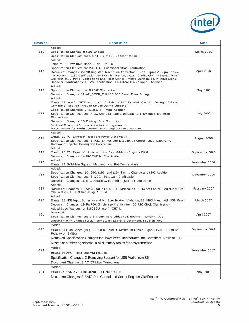
Revision Description Date
-001 Initial Release. April 2005
-002
Added:Errata: 2-SATA AHCI Recovery From Task File Error, 3-PCI Express* Completion Timer in L1, 4-3 Gb/s SATA Signal Voltage Level.Specification Clarifications: 1-PATA Secondary Command/Control BAR, 2-AHCI Operation Clarification.
May 2005
-003
Added:Errata: 5-SATA Index/Data Pair Decode, 6-SATA 3 Gb/s Squelch Event, 7-PCI Express* False Correctable Error.Specification Changes: 1-SATA Capability Registers Disable Change, 2-IOL1/Intel® IOH 1 Change, 3-INTVRMEN Input Threshold Change.Specification Clarifications: 3-AHCI Host Capability Register Change, 4-PCI Express* One x4 Clarification, 5-ASF Configuration Registers Clarification, 6-SM Bus Slave Read Tables, 7-Feature Detection Capability, 8-PME Pending, 9-Indeterminate State Before Power Stable.
June 2005
-004
Modified:Specification Clarification: 1-PATA Secondary Command/Control BAR.Added:Specification Clarification: 10-SATA Electrical Specification Clarification.
August 2005
-005
Specification Clarifications: 11-SPI Timings Corrections and 12-F0h Read Behavior Clarifications.Document Changes: 2-DC Current Characteristics Note Correction and 3-PCI Functional Description Correction.
September 2005
-006
Specification Clarifications: 13-PCI Downstream Device Disable Clarification, 14-Processor Initiated Passive Cooling Clarification, 15-LPC SERR Generation Behavior Clarification, and 16-t302 Clarification.Document Changes: 4-THRMTRIP# Timing Correction, 5-LSTS Note Correction, and 6-AHCI CAP.SALP Attribute Correction.
October 2005
-007
Added:Specification Change: 4-Clock Gating Support Specification Change.Document Changes: 7-Interrupt Pin Register Reserved Bits Correction, 8-PCI Express* Slot Power Register Description Additions, 9-GPIO Number Documentation Correction, and 10-USB Port Number Documentation Corrections.
November 2005
-008Added:Specification Change: 5-Clock Gating Register ReservedDocument Change: 11-LPC Cycle Change
December 2005
-009
Moved all Specification Changes, Specification Clarifications and Documentation Changes into parent datasheet (307013-002)Modified:Document Changes: 1- PCI Device Revision IDAdded: Intel® ICH7DH, ICH7M, and ICH7M DH MarksErrata: 8-PCI Express* Scrambling, 9-Intel® ICH7M LPC and DMI L1, 10-Intel® ICH7M Intel® PRO/Wireless 3945ABG mode False Correctable Error during FTS with L0s, 11-Intel® ICH7M USB LS/FS Device behind a USB HS Hub, 12-Intel® ICH7M High Definition Audio Dynamic Clock Gating, 13-Intel® ICH7M PCI Dynamic Gating, 14-Intel® ICH7M Intel® PRO/Wireless 3945ABG Host Interface Auto-Detect, 15-Intel® ICH7M PCI Express*Root Port Transmission SKP Sequence during L1 Entry
January 2006
-010Added:Specification Change: 6-GPIO25 Functional Strap ChangeSpecification Change: 7-Intel® ICH7M SKU Change
February 2006
Intel® I/O Controller Hub 7 (Intel® ICH 7) FamilySeptember 2013 Specification UpdateDocument Number: 307014-033US 5
-011Added:Specification Change: 8-t200 ChangeSpecification Clarification: 1-GNT[5:0]# Pull-up Clarification
March 2006
-012
Added:Erratum: 16-MW DMA Mode-1 Tdh ErratumSpecification Clarification: 2-GPIO25 Functional Strap ClarificationDocument Changes: 2-ESD Register Description Correction, 3-PCI Express* Signal Name Correction, 4-t290 Clarification, 5-t293 Clarification, 6-t294 Clarification, 7-Signal “Type” Clarification, 8-Power Sequencing and Reset Signal Timings Clarification, 9-Input Signal Behavior Clarifications, 10-Vcc Clarification, 11-ATA/ATAPI-7 Support Addition
April 2006
-013Added:Specification Clarification: 3-t232 ClarificationDocument Changes: 12-AZ_DOCK_EN#/GPIO33 Power Plane Change
May 2006
-014
Added:Errata: 17-Intel® ICH7M and Intel® ICH7M-DH UHCI Dynamic Clocking Gating, 18-Reset Command Received Through SMBus During SuspendSpecification Changes: 9-RSMRST# Timing AdditionSpecification Clarifications: 4-DC Characteristic Clarifications, 5-SMBus Slave Write ClarificationDocument Changes: 13-Package Size CorrectionModified Erratum #3 to correct a formatting error. Miscellaneous formatting corrections throughout the document.
July 2006
-015
Added:Errata: 19-PCI Express* Root Port Power State ValueSpecification Clarifications: 6-PM1_EN Register Description Correction, 7-D29:F7 PCI Command Register Description Correction.
August 2006
-016Added:Errata: 20-PCI Express* Upstream Link Base Address Register Bit 0Document Changes: 14-BIOSWE Bit Clarification
September 2006
-017Added:Errata: 21-SATA Min Squelch Marginality at Hot Temperature
November 2006
-018
Added:Specification Changes: 10-t290, t293, and t294 Timing Change and t303 AdditionSpecification Clarifications: 8-t290, t293, t294 ClarificationDocument Changes: 15-RTC Update Cycle Inhibit (SET) bit Correction
December 2006
-019Added:Document Changes: 16-APIC Enable (AEN) Bit Clarification, 17-Reset Control Register (CF9h) Clarification, 18-TP3 Replacing RTEST#
February 2007
-020Added:Errata: 22-IDE Input Buffer V+and Vih Specification Violation, 23-UHCI Hang with USB ResetDocument Changes: 19-PWROK Glitch-free Clarification, 20-RTC Clock Clarification
March 2007
-021
Added Specifications for 82801GU Intel® ICH7-URemoved:Specification Clarifications 1-8. Items were added to Datasheet, Revision -003.Documentation Changes 2-20. Items were added to Datasheet, Revision -003.
April 2007
-022Added:
Errata: 24-High Speed (HS) USB2.0 D+ and D- Maximum Driven Signal Level, 25-THRM Polarity on SMBus
September 2007
-023
Removed Specification Changes that have been incorporated into Datasheet, Revision -003.
Reset the numbering scheme in all summary tables for easy reference.
Added:
Errata: 26-AHCI Reset and MSI Request
Specification Changes: 2-Removing Support for USB Wake from S5
Document Changes: 2-AC ’97 Misc Corrections.
November 2007
-024
Added:
Errata:27-SATA Gen1 Initialization / LPM Erratum
Document Changes: 3-SATA Port Control and Status Register Clarification
May 2008
Revision Description Date
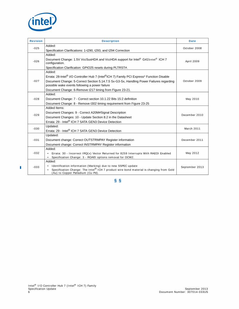
Intel® I/O Controller Hub 7 (Intel® ICH 7) FamilySpecification Update September 20136 Document Number: 307014-033US
§ §
-025Added:
Specification Clarifications: 1-t290, t293, and t294 CorrectionOctober 2008
-026
Added:
Document Change: 1.5V VccSusHDA and VccHDA support for Intel® G41\Intel® ICH 7 configuration.
Specification Clarification: GPIO25 resets during PLTRST#.
April 2009
-027
Added:
Errata: 28-Intel® I/O Controller Hub 7 (Intel®ICH 7) Family PCI Express* Function Disable
Document Change: 5-Correct Section 5.14.7.5 Sx-G3-Sx, Handling Power Failures regarding possible wake events following a power failure
Document Change: 6-Remove t217 timing from Figure 23-21.
October 2009
-028
Added:
Document Change: 7 - Correct section 10.1.22 Bits 15:2 definition
Document Change: 8 - Remove t302 timing requirement from Figure 23-25
May 2010
-029
Added Items:
Document Changes: 9 - Correct A20M#Signal Description
Document Changes: 10 - Update Section 8.2 in the Datasheet
Errata: 29 - Intel® ICH 7 SATA GEN3 Device Detection
December 2010
-030Updated:
Errata: 29 - Intel® ICH 7 SATA GEN3 Device DetectionMarch 2011
-031
Updated:
Document change: Correct OUTSTRMPAY Register information
Document change: Correct INSTRMPAY Register information
December 2011
-032Added:
• Errata: 30 - Incorrect IRQ(x) Vector Returned for 8259 Interrupts With RAEOI Enabled• Specification Change: 3 - ROAEI options removal for OCW2.
May 2012
-033
Added:
• Identification information (Marking) due to new SSPEC update• Specification Change: The Intel® ICH 7 product wire bond material is changing from Gold
(Au) to Copper Palladium (Cu-Pd).
September 2013
Revision Description Date

Intel® I/O Controller Hub 7 (Intel® ICH 7) FamilySeptember 2013 Specification UpdateDocument Number: 307014-033US 7
Preface
This document is an update to the specifications contained in the Affected Documents/Related Documents table below. This document is a compilation of device and documentation errata, specification clarifications and changes. It is intended for hardware system manufacturers and software developers of applications, operating systems, or tools.
Information types defined in Nomenclature are consolidated into the specification update and are no longer published in other documents.
This document may also contain information that was not previously published.
Affected Documents/Related Documents
NomenclatureErrata are design defects or errors. Errata may cause the Intel® ICH 7's behavior to deviate from published specifications. Hardware and software designed to be used with any given stepping must assume that all errata documented for that stepping are present in all devices.
Specification Changes are modifications to the current published specifications. These changes will be incorporated in any new release of the specification.
Specification Clarifications describe a specification in greater detail or further highlight a specification’s impact to a complex design situation. These clarifications will be incorporated in any new release of the specification.
Documentation Changes include typos, errors, or omissions from the current published specifications. These will be incorporated in any new release of the specification.
Note: Errata remain in the specification update throughout the product’s life cycle, or until a particular stepping is no longer commercially available. Under these circumstances, errata removed from the specification update are archived and available upon request. Specification changes, specification clarifications and documentation changes are removed from the specification update when the appropriate changes are made to the appropriate product specification or user documentation (datasheets, manuals, etc.).
§ §
Title Document Number
Intel® I/O Controller Hub 7 (ICH7) Family Datasheet 307013-003
Intel® I/O Controller Hub 7 (Intel® ICH 7) FamilySpecification Update September 20138 Document Number: 307014-033US
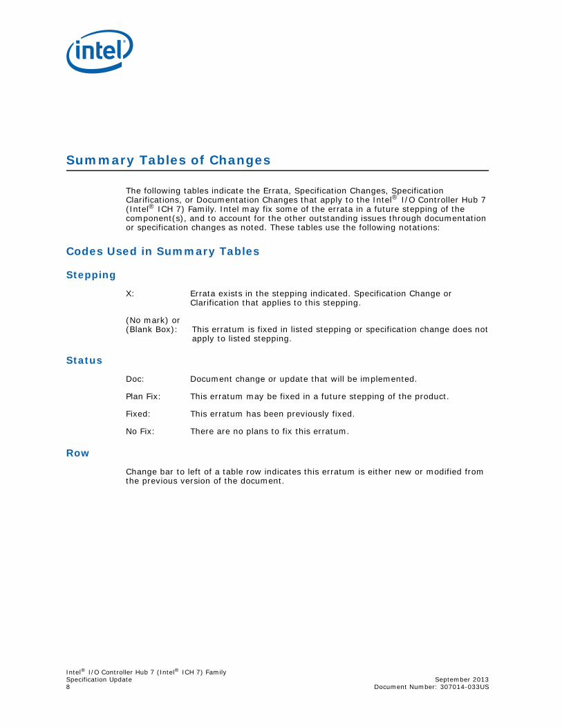
Summary Tables of Changes
The following tables indicate the Errata, Specification Changes, Specification Clarifications, or Documentation Changes that apply to the Intel® I/O Controller Hub 7 (Intel® ICH 7) Family. Intel may fix some of the errata in a future stepping of the component(s), and to account for the other outstanding issues through documentation or specification changes as noted. These tables use the following notations:
Codes Used in Summary Tables
Stepping
X: Errata exists in the stepping indicated. Specification Change or Clarification that applies to this stepping.
(No mark) or (Blank Box): This erratum is fixed in listed stepping or specification change does not
apply to listed stepping.
Status
Doc: Document change or update that will be implemented.
Plan Fix: This erratum may be fixed in a future stepping of the product.
Fixed: This erratum has been previously fixed.
No Fix: There are no plans to fix this erratum.
Row
Change bar to left of a table row indicates this erratum is either new or modified from the previous version of the document.
Intel® I/O Controller Hub 7 (Intel® ICH 7) FamilySeptember 2013 Specification UpdateDocument Number: 307014-033US 9
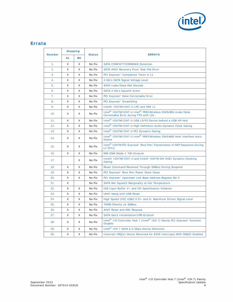
Errata
NumberStepping
Status ERRATAA1 B0
1. X X No Fix SATA COMINIT/COMWAKE Detection
2. X X No Fix SATA AHCI Recovery From Task File Error
3. X X No Fix PCI Express* Completion Timer in L1
4. X X No Fix 3 Gb/s SATA Signal Voltage Level
5. X X No Fix SATA Index/Data Pair Decode
6. X X No Fix SATA 3 Gb/s Squelch Event
7. X X No Fix PCI Express* False Correctable Error
8. X X No Fix PCI Express* Scrambling
9. X X No Fix Intel® ICH7M/ICH7-U LPC and DMI L1
10. X X No Fix Intel® ICH7M/ICH7-U Intel® PRO/Wireless 3945ABG mode False Correctable Error during FTS with L0s
11. X X No Fix Intel® ICH7M/ICH7-U USB LS/FS Device behind a USB HS Hub
12. X X No Fix Intel® ICH7M/ICH7-U High Definition Audio Dynamic Clock Gating
13. X X No Fix Intel® ICH7M/ICH7-U PCI Dynamic Gating
14. X X No Fix Intel® ICH7M/ICH7-U Intel® PRO/Wireless 3945ABG Host Interface Auto-Detect
15. X X No Fix Intel® ICH7M PCI Express* Root Port Transmission of SKP Sequence During L1 Entry
16. X X No Fix MW DMA Mode-1 Tdh Erratum
17. X No Fix Intel® ICH7M/ICH7-U and Intel® ICH7M-DH UHCI Dynamic Clocking Gating
18. X X No Fix Reset Command Received Through SMBus During Suspend
19. X X No Fix PCI Express* Root Port Power State Value
20. X X No Fix PCI Express* Upstream Link Base Address Register Bit 0
21. X No Fix SATA Min Squelch Marginality at Hot Temperature
22. X X No Fix IDE Input Buffer V+ and Vih Specification Violation
23. X X No Fix UHCI Hang with USB Reset
24. X X No Fix High Speed (HS) USB2.0 D+ and D- Maximum Driven Signal Level
25. X X No Fix THRM Polarity on SMBus
26. X X No Fix AHCI Reset and MSI Request
27. X X No Fix SATA Gen1 Initialization/LPM Erratum
28. X X No Fix Intel® I/O Controller Hub 7 (Intel® ICH 7) Family PCI Express* Function Disable
29. X X No Fix Intel® ICH 7 SATA 6.0 Gbps Device Detection
30. X X No Fix Incorrect IRQ(x) Vector Returned for 8259 Interrupts With RAEOI Enabled
Intel® I/O Controller Hub 7 (Intel® ICH 7) FamilySpecification Update September 201310 Document Number: 307014-033US
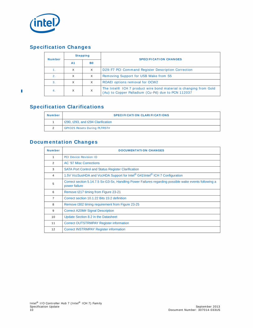
Specification Changes
NumberStepping
SPECIFICATION CHANGESA1 B0
1. X X D29:F7 PCI Command Register Description Correction
2. X X Removing Support for USB Wake from S5
3. X X ROAEI options removal for OCW2
4. X XThe Intel® ICH 7 product wire bond material is changing from Gold (Au) to Copper Palladium (Cu-Pd) due to PCN 112037
Specification ClarificationsNumber SPECIFICATION CLARIFICATIONS
1 t290, t293, and t294 Clarification
2 GPIO25 Resets During PLTRST#
Documentation ChangesNumber DOCUMENTATION CHANGES
1 PCI Device Revision ID
2 AC ’97 Misc Corrections
3 SATA Port Control and Status Register Clarification
4 1.5V VccSusHDA and VccHDA Support for Intel® G41\Intel® ICH 7 Configuration
5Correct section 5.14.7.5 Sx-G3-Sx, Handling Power Failures regarding possible wake events following a power failure
6 Remove t217 timing from Figure 23-21
7 Correct section 10.1.22 Bits 15:2 definition
8 Remove t302 timing requirement from Figure 23-25
9 Correct A20M# Signal Description
10 Update Section 8.2 in the Datasheet
11 Correct OUTSTRMPAY Register information
12 Correct INSTRMPAY Register information
Intel® I/O Controller Hub 7 (Intel® ICH 7) FamilySeptember 2013 Specification UpdateDocument Number: 307014-033US 11
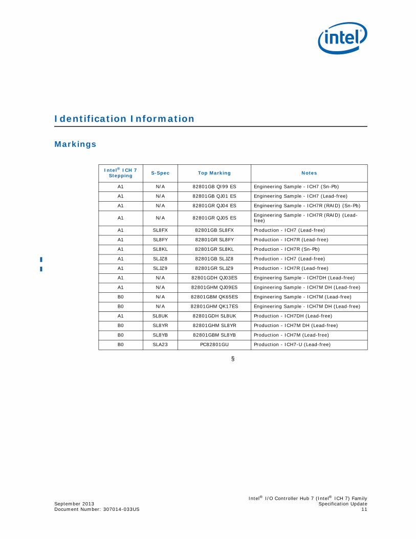
Identification Information
Markings
§
Intel® ICH 7 Stepping S-Spec Top Marking Notes
A1 N/A 82801GB QI99 ES Engineering Sample - ICH7 (Sn-Pb)
A1 N/A 82801GB QJ01 ES Engineering Sample - ICH7 (Lead-free)
A1 N/A 82801GR QJ04 ES Engineering Sample - ICH7R (RAID) (Sn-Pb)
A1 N/A 82801GR QJ05 ES Engineering Sample - ICH7R (RAID) (Lead-free)
A1 SL8FX 82801GB SL8FX Production - ICH7 (Lead-free)
A1 SL8FY 82801GR SL8FY Production - ICH7R (Lead-free)
A1 SL8KL 82801GR SL8KL Production - ICH7R (Sn-Pb)
A1 SLJZ8 82801GB SLJZ8 Production - ICH7 (Lead-free)
A1 SLJZ9 82801GR SLJZ9 Production - ICH7R (Lead-free)
A1 N/A 82801GDH QJ03ES Engineering Sample - ICH7DH (Lead-free)
A1 N/A 82801GHM QJ09ES Engineering Sample - ICH7M DH (Lead-free)
B0 N/A 82801GBM QK65ES Engineering Sample - ICH7M (Lead-free)
B0 N/A 82801GHM QK17ES Engineering Sample - ICH7M DH (Lead-free)
A1 SL8UK 82801GDH SL8UK Production - ICH7DH (Lead-free)
B0 SL8YR 82801GHM SL8YR Production - ICH7M DH (Lead-free)
B0 SL8YB 82801GBM SL8YB Production - ICH7M (Lead-free)
B0 SLA23 PC82801GU Production - ICH7-U (Lead-free)
Intel® I/O Controller Hub 7 (Intel® ICH 7) FamilySpecification Update September 201312 Document Number: 307014-033US
Errata
1. SATA COMINIT/COMWAKE DetectionProblem: During Out-Of-Band (OOB) sequencing, the Intel® ICH 7 may detect COMINIT/
COMWAKE when only 2 or 3 bursts of ALIGNs are received from the SATA deviceinstead of the required 4 bursts as per the SATA 1.0a Specification.
Implication: None Known - The Intel® ICH 7 appropriately handles subsequent ALIGNs.Workaround:None.Status: No Fix. For steppings affected, see the Summary Tables of Changes.
2. SATA AHCI Recovery From Task File ErrorProblem: During an AHCI fatal error condition, if the device signals a Task File Error (TFES), the
Intel® ICH 7 may not be able to recover correctly after software performs the AHCIspec-defined fatal error recovery mechanism.
Implication: SATA port will appear busy resulting in the device being inaccessible.
Note: IAA/IMST 4.0 and later implements a reset mechanism that does not allow this issue to be exposed. Furthermore this condition has only been replicated in a synthetic test environment.
Workaround:AHCI driver should toggle the ST bit to ‘1’ and back to ‘0’ upon detecting TFES bit setafter ST bit is cleared.
Status: No Fix. For steppings affected, see the Summary Tables of Changes.
3. PCI Express* Completion Timer in L1Problem: The Intel® ICH 7 PCI Express* Completion Timer always halts when the PCI Express*
link enters the L1 state. According to the PCI Express specification, Rev 1.0a, the timershould continue running during Active State Power Management (ASPM)-initiated L1states.
Implication: No known implications with devices that meet the PCI Express* 1.0a specification.
The system may hang if a PCI Express* device enters the ASPM L1 state before sending all completions for an outstanding non-posted request. Note that since the PCI Express* specification requires that endpoints send all pending completions before entering ASPM L1, a system hang of this nature requires a device that is not fully compliant with the PCI Express* specification. This issue has only been replicated in a synthetic environment.
Workaround:None.Status: No Fix. For steppings affected, see the Summary Tables of Changes.
Intel® I/O Controller Hub 7 (Intel® ICH 7) FamilySeptember 2013 Specification UpdateDocument Number: 307014-033US 13
4. 3 Gb/s SATA Signal Voltage LevelProblem: The Intel® ICH 7 3 Gb/s SATA transmit buffers have been designed to maximize
performance and robustness over a variety of routing scenarios. As a result, the Intel® ICH 7 SATA transmit signaling voltage levels may exceed the maximummotherboard TX connector and device RX connector voltage specifications (section6.2.1 of Serial ATA II Electrical Specification, Rev 1.0).
Implication: None known.Workaround:None.Status: No Fix. For steppings affected, see the Summary Tables of Changes.
5. SATA Index/Data Pair DecodeProblem: The Intel® ICH 7 SATA controller does not properly decode SATA index/data pair
transactions when I/O trapping is enabled.Implication: SATA index/data pair accesses are not required for Intel® ICH 7 configuration or
functionality. If I/O trapping is enabled, SATA index/data pair register access mayreturn unexpected data.
Workaround:BIOS workaround available. Contact your Intel field Representative for details.Status: No Fix. For steppings affected, see the Summary Tables of Changes.
6. SATA 3 Gb/s Squelch EventProblem: When subjected to a specific high-frequency test pattern for an extended time period
with a very low receive amplitude at the motherboard connector, the Intel® ICH 7 mayinaccurately detect a squelch event when the SATA link is operating at 3 Gb/s.
Implication: A squelch event may cause the 3 Gb/s SATA device to become unavailable and/or thesystem may hang. Note: this issue has only been replicated in an artificial testenvironment and has not been reported with known SATA devices. No applicationfailures have been observed in a real world environment.
Workaround:None.Status: No Fix. For steppings affected, see the Summary Tables of Changes.
7. PCI Express* False Correctable ErrorProblem: During L0s and/or L1 entry or exit on the PCI Express* root ports, the Intel® ICH 7
may acknowledge a correctable error, which violates the PCI Express* spec, 1.0a. Thisis reported thru the Correctable Error Detected bit (D28:F0/F1/F2/F3/F4/F5:Offset4Ah:bit-0) and the Receiver Error Status bit (D28:F0/F1/F2/F3/F4/F5:Offset 150h: bit-0).
Implication: No system functionality issues observed. However, correctable error logging may notaccurately report the number of errors.
Note: No known end-user SW uses this logging capability.Workaround:None.Status: No Fix. For steppings affected, see the Summary Tables of Changes.
Intel® I/O Controller Hub 7 (Intel® ICH 7) FamilySpecification Update September 201314 Document Number: 307014-033US
8. PCI Express* ScramblingProblem: While entering the Recovery state, the Intel® ICH 7 stops scrambling two symbols
before the first TS (training sequence).Implication: When these non-scrambled symbols are received by the endpoint, the de-scrambler of
the endpoint will observe two symbols of random data. The first symbol of TS1 willreset the endpoint’s de-scrambler so that the endpoint should recognize the TS1 andTS2 ordered-sets being transmitted and move into the Recovery state as planned.
There is no system level impact if the endpoint is PCI Express* Specification 1.0a compliant in ignoring the random data.
Workaround:None.Status: No Fix. For steppings affected, see the Summary Tables of Changes.
9. Intel® ICH7M/ICH7-U LPC and DMI L1Problem: Under certain circumstances ICH7M/ICH7-U may initiate DMI L1 entry outside of C3/C4
while intermittent burst transfers are occurring by a LPC bus master.Implication: Possible long latency when transferring data by a LPC bus master device due to L1 exit
latency.Workaround:BIOS workaround available. Contact your Intel field representative for details.Status: No Fix. For steppings affected, see the Summary Tables of Changes.
10. Intel® ICH7M/ICH7-U Intel® PRO/Wireless 3945ABG mode False Correctable Error during FTS with L0s
Problem: During L0s exit, the Intel® ICH 7 may erroneously report correctable receiver errorswhile the PCI Express* link is operating in Intel® PRO/Wireless 3945ABG mode. This isreported thru the Correctable Error Detected bit (D28:F0/F1/F2/F3/F4/F5:Offset 4Ah:bit 0) and the Receiver Error Status bit (D28:F0/F1/F2/F3/F4/F5:Offset 150h: bit 0).
Implication: No system functionality issues observed. However, correctable error logging may notaccurately report the number of errors. Note: No known end-user SW uses this loggingcapability.
Workaround:None.Status: No Fix. For steppings affected, see the Summary Tables of Changes.
11. Intel® ICH7M/ICH7-U USB LS/FS Device behind a USB HS HubProblem: Intel® ICH7M/ICH7-U incorrectly processes a split transaction when a USB Low Speed/
Full Speed device is connected to Intel® ICH7M/ICH7-U through a USB High SpeedHub.
Implication: Some USB Low Speed/Full Speed devices may not function properly when connected tothe Intel® ICH7M/ICH7-U root port through a USB High Speed hub.
Workaround:BIOS workaround available. Contact your Intel field representative for details.Status: No Fix. For steppings affected, see the Summary Tables of Changes.
12. Intel® ICH7M/ICH7-U High Definition Audio Dynamic Clock GatingProblem: Intel® ICH7M/ICH7-U may access incorrect memory location when a High Definition
Audio device is installed and High Definition Audio dynamic clock gating is enabled.Implication: Some High Definition Audio devices may not function properly with Intel® ICH7M/ICH7-
U and may result in a NMI.Workaround:BIOS workaround available. Contact your Intel field representative for details.Status: No Fix. For steppings affected, see the Summary Tables of Changes.

Intel® I/O Controller Hub 7 (Intel® ICH 7) FamilySeptember 2013 Specification UpdateDocument Number: 307014-033US 15
13. Intel® ICH7M/ICH7-U PCI Dynamic GatingProblem: Intel® ICH7M/ICH7-U PCI Dynamic gating feature introduced a circuit isolation
problem.Implication: Use of PCI Dynamic Gating can severely impact product functionality.Workaround:BIOS must ensure PCI Dynamic Gating is disabled. BIOS must ensure RCBA +
341Ch[16] = 0 during boot and resume sequence. Contact your Intel fieldrepresentative for details.
Status: No Fix. For steppings affected, see the Summary Tables of Changes.
14. Intel® ICH7M/ICH7-U Intel® PRO/Wireless 3945ABG Host Interface Auto-Detect
Problem: During the Intel® ICH7M/ICH7-U auto-detect sequence for Intel® PRO/Wireless3945ABG host interface mini-card device, there is a potential failure due to a timing,voltage, and temperature related boundary condition. Failure occurs only with Intel® PRO/Wireless 3945ABG mini-card devices.
Implication: Intermittent enumeration failures may occur with Intel® PRO/Wireless 3945ABG mini-card devices on Intel® ICH7M/ICH7-U-based platforms.
Workaround:BIOS workaround available. Contact your Intel field representative for details.Status: No Fix. For steppings affected, see the Summary Tables of Changes.
15. Intel® ICH7M PCI Express* Root Port Transmission of SKP Sequence During L1 Entry
Problem: During L1 entry, Intel® ICH7M currently follows the PCI Express* Spec 1.0a section5.3.2.1 and transmits a continuous stream of PM Request ACK DLLPs but will not sendSKP ordered sets, as permitted by PCI Express* specification errata C7, even if theinterval between SKPordered set has exceeded the 1180 to 1538 symbol times.
Implication: With certain receiver designs that are incapable of tolerating this sequence, in suchsystems a hang or NMI may occur.
Workaround:NoneStatus: No Fix. For steppings affected, see the Summary Tables of Changes.
16. MW DMA Mode-1 Tdh ErratumProblem: Data hold time of MW DMA Mode-1 writes may not meet ATA specification.Implication: None known.Workaround:Program the controller to PIO Mode-4 instead.Status: No Fix. For steppings affected, see the Summary Tables of Changes.
Intel® I/O Controller Hub 7 (Intel® ICH 7) FamilySpecification Update September 201316 Document Number: 307014-033US
17. Intel® ICH7M/ICH7-U and Intel® ICH7M-DH UHCI Dynamic Clocking Gating
Problem: With Intel® ICH7M/ICH7-U and Intel® ICH7M-DH UHCI Dynamic Clock Gating enabled,under certain conditions, toggling the UHCI Controller Run/Stop control bit may resultin the controller continuously accessing the Transaction Description Link List via DMAcycles.
• The condition may occur when clearing the UHCI Run/Stop bit between initiation and completion of an upstream UHCI memory request.
• The condition may occur with either Low-speed/Full-speed devices populated or unpopulated.
• Affects platforms with Intel® ICH7M/ICH7-U and Intel® ICH7M-DH, when UHCI Dynamic Clock Gating is enabled
Implication: The system may not enter a C-state due to continuous DMA traffic.• A system hang may occur when entering S3/4/5 sleep state.• The system hang case has been observed with USB Wake support enabled.
Workaround:BIOS workaround available. Contact your Intel field representative for details.Status: No Fix. For steppings affected, see the Summary Tables of Changes.
18. Reset Command Received Through SMBus During SuspendProblem: If the Intel® ICH 7 is sent a ‘Hard Reset Without Cycling’ command on SMBus while the
system is in S3, the reset command will not be executed until the next wake event. TheASF Spec, rev 1.03, requires the Intel® ICH 7 to execute the Hard Reset WithoutCycling immediately.
Implication: SMBus write commands that are sent after the Hard Reset Without Cycling commandand before the wake event will be NAKed by the Intel® ICH 7. This also applies to anySMBus wake commands sent after a Hard Reset Without Cycling command, such thatthe SMBus wake command will not cause the system to wake.
Note: Intel® Active Management Technology is not impacted as Intel® AMT does not use the Hard Reset Without Cycling command while the system is in S3.
Note: Any SMBus read that is accepted by the Intel® ICH 7 will complete normallyWorkaround:Do not send a Hard Reset Without Cycling command while the system is in S3.
Note: Exposure to this issue can be reduced by issuing a wake command prior to issuing the Hard Reset Without Cycling command.
Status: No Fix. For steppings affected, see the Summary Tables of Changes.
19. PCI Express* Root Port Power State ValueProblem: The Intel® ICH 7 PCI Express* root ports support the D3 and D0 states, but also accept
writes of values corresponding to the D2 and D1 states in the Power State bit field ofthe Power Management Control and Status registers (D28:F0/F1/F2/F3/F4/F5:A4h).The Intel® ICH 7 PCI Express* root port PCI Power Management Capabilities Registers(D28:F0/F1/F2/F3/F4/F5:A2h) do not claim support of D2 and D1 power states.
Implication: No functional implications known. Writes of values corresponding to the D2 and D1states (i.e., 10b or 01b) do not cause behavioral changes within the Intel® ICH 7, butthe value is displayed in the Power State bit field.
Workaround:Software should not write unsupported power state values (i.e., 10b or 01b) to thePower State bit field of the Power Management Control and Status register.
Status: No Fix. For steppings affected, see the Summary Tables of Changes.
Intel® I/O Controller Hub 7 (Intel® ICH 7) FamilySeptember 2013 Specification UpdateDocument Number: 307014-033US 17
20. PCI Express* Upstream Link Base Address Register Bit 0Problem: The Intel® ICH 7 PCI Express* root ports’ Upstream Link Base Address (ULBA) Register
(D28:F0/F1/F2/F3/F4/F5:198h) bit 0 mirrors the value of bit 0 in the Intel® ICH 7RCBA register (D31:F0:F0h). During normal system operation, bit 0 of the RCBAregister is set to 1. This results in bit 0 of the ULBA also being set to 1. The PCIExpress* specification, rev 1.0a, requires that bit 0 of the ULBA be 0.
Implication: No functional implications known.Workaround:None. Status: No Fix. For steppings affected, see the Summary Tables of Changes.
21. SATA Min Squelch Marginality at Hot TemperatureProblem: The Intel® ICH 7 SATA min squelch voltage may violate the SATA specification at case
temperature of 85°C or above.Implication: Squelch violation may cause a SATA drive detection failure resulting in either error
message or blue screen, depending on the drive being re-detected and the type ofdetection scenario that is occurring: boot, system reset, active power management,resume from S3-S5, or when an error on the SATA wire is experienced.
Note: The Intel® ICH 7 case temperature is not typically above 85°C during these drive detection scenarios.
Workaround:None.
Note: Exposure to the issue can be eliminated through effective system thermal design.Status: No Fix. For steppings affected, see the Summary Tables of Changes.
22. IDE Input Buffer V+ and Vih Specification ViolationProblem: Under maximum voltage condition of the Vcc3_3 power rail (3.465 V), the Intel® ICH 7
may violate the PATA IDE V+ max (low-to-high input threshold) and Vih2 min (inputhigh voltage) specifications. The limit in both cases is specified as 2.0 V.
Implication: The Intel® ICH 7 may not switch on a low-to-high transition until V+ max is at 2.1 V,and may not register a logic high until Vih2 min is at 2.1 V.
There is no known impact to system functionality. This issue has only been seen in a synthetic test environment, as an IDE device typically drives the input to 3.3 V.
Workaround:None.Status: No fix.For steppings affected, see the Summary Tables of Changes.
23. UHCI Hang with USB ResetProblem: When SW initiates a Host Controller Reset or a USB Global Reset while concurrent
traffic occurs on at least three UHCI controllers, the UHCI controller(s) may hang.
The issue has only been replicated in a synthetic reset test environment.Implication: System may hang.Workaround:BIOS workaround available. Contact your Intel field representative for more details.Status: No fix. For steppings affected, see the Summary Tables of Changes.
Intel® I/O Controller Hub 7 (Intel® ICH 7) FamilySpecification Update September 201318 Document Number: 307014-033US
24. High Speed (HS) USB2.0 D+ and D- Maximum Driven Signal LevelProblem: During Start-of-Packet (SOP)/End-of-Packet (EOP), the Intel® ICH 7 may drive D+ and
D- lines to a level greater than USB 2.0 spec +/-200mV max.Implication: May cause High Speed (HS) USB 2.0 devices to be unrecognized by OS or may not be
readable/writable if the following two conditions are met:• The receiver is pseudo differential design• The receiver is not able to ignore SE1 (single-ended) state
Note: Intel has only observed this issue with a motherboard down HS USB 2.0 device using pseudo differential design. This issue will not affect HS USB 2.0 devices with complementary differential design or Low Speed (LS) and Full Speed (FS) devices.
Workaround:None.Status: No Fix. For steppings affected, see the Summary Tables of Changes.
25. THRM Polarity on SMBusProblem: When THRM#_POL (PMBASE+42h:bit0) is set to high, the THRM# pin state as reported
to the SMBus TCO unit is logically inverted.Implication: If the THRM#_POL bit is set to high, an external SMBus master reading the BTI
Temperature Event status will not receive the correct state of the THRM# pin. The valuewill be logically inverted. If THRM#_POL set to low, value is correct.
Workaround:None.Status: No Fix. For steppings affected, see the Summary Tables of Changes.
26. AHCI Reset and MSI RequestProblem: If the Intel® ICH 7 AHCI SATA controller receives a HBA reset while MSI interrupts are
enabled, a boundary condition exists where the Intel® ICH 7 SATA controller mayrespond to a non-posted request that is intended for another Intel® ICH 7 function.
Implication: Issue has only been observed in a synthetic test environment. Unexpected systembehavior may occur. System implication may vary depending on the non-postedrequest that is fulfilled.
Note: Intel® Matrix Storage Manager AHCI driver does not use the HBA reset command. Linux may enable MSIs and use the HBA reset command. No other third-party software known to utilize MSI interrupts.
Workaround:Prior to performing an HBA reset, software should disable AHCI interrupts by writing a‘0’ to Interrupt Enable bit (ABAR+04h, bit 1) and then perform a read to the AHCI GHCregister (ABAR+04h).
Status: No Fix.

Intel® I/O Controller Hub 7 (Intel® ICH 7) FamilySeptember 2013 Specification UpdateDocument Number: 307014-033US 19
27. SATA Gen1 Initialization/LPM ErratumProblem: During SATA Initialization routines or while resuming from a Link Power Managed (LPM)
state, the Intel® ICH 7 SATA link to Gen1 (1.5 Gb/s) devices may fail to be established.Implication: One or more of the following symptoms may occur:
• During Boot or Resume from S4/S5: SATA Gen1 devices may not be detected, resulting in "Operating System Not Found" error.
• During Resume from S3: System may hang when attempting to initialize SATA Gen1 devices.
• During S0: If LPM is enabled and ALL SATA Gen1 devices within the system support LPM, slow SATA Gen1 performance may occur.
Workaround:BIOS workaround available. Contact your Intel field representative for more details.Status: No Fix. For steppings affected, see the Summary Table of Changes.
28. Intel® I/O Controller Hub 7 (Intel® ICH 7) Family PCI Express* Function Disable
Problem: Intel® ICH 7 Family PCI Express* [1:6] Disable bit in Function Disable Register may notput the PCI Express* port into a link down state if a PCI Express* device is attached.
Implication: Intel® ICH7-M:
PCI Express* port [1:6] with a PCI Express* device attached may remain in L0 stateand DMI may not be able to go into L1 state.
Intel®ICH7, ICH7R, ICH7DH, ICH7-M DH, and ICH7-U:
PCI Express* port [1:6] with a PCI Express* device attached may remain in L0 state.Workaround:A BIOS code change has been identified.Status: No Fix. For steppings affected, see the Summary Table of Changes.
29. Intel® ICH 7 SATA 6.0 Gbps Device DetectionProblem: Intel® ICH 7 may not be able to complete SATA Out Of Band (OOB) Signaling with SATA
6.0 Gbps Devices and down shift to SATA 3.0 Gbps speed.Implication: Intel® ICH 7 may not detect SATA 6.0 Gbps Devices upon power up or resume from S3,
S4 or S5 State.Workaround:None.Status: No Plan to Fix. For steppings affected, see the Summary Table of Changes.
30. Incorrect IRQ(x) Vector Returned for 8259 Interrupts With RAEOI Enabled
Problem: If multiple interrupts are active prior to an interrupt acknowledge cycle with RotatingAutomatic End of Interrupt (RAEOI) mode of operation enabled for 8259 interrupts (0-7), an incorrect IRQ(x) vector may be returned to the CPU.
Implication: Implications of an incorrect IRQ(x) vector being returned to the CPU are SWimplementation dependent.
Note: This issue has only been observed in a synthetic test environment.Workaround:None.Status: No Plan to Fix. For steppings affected, see the Summary Table of Changes.
§ §
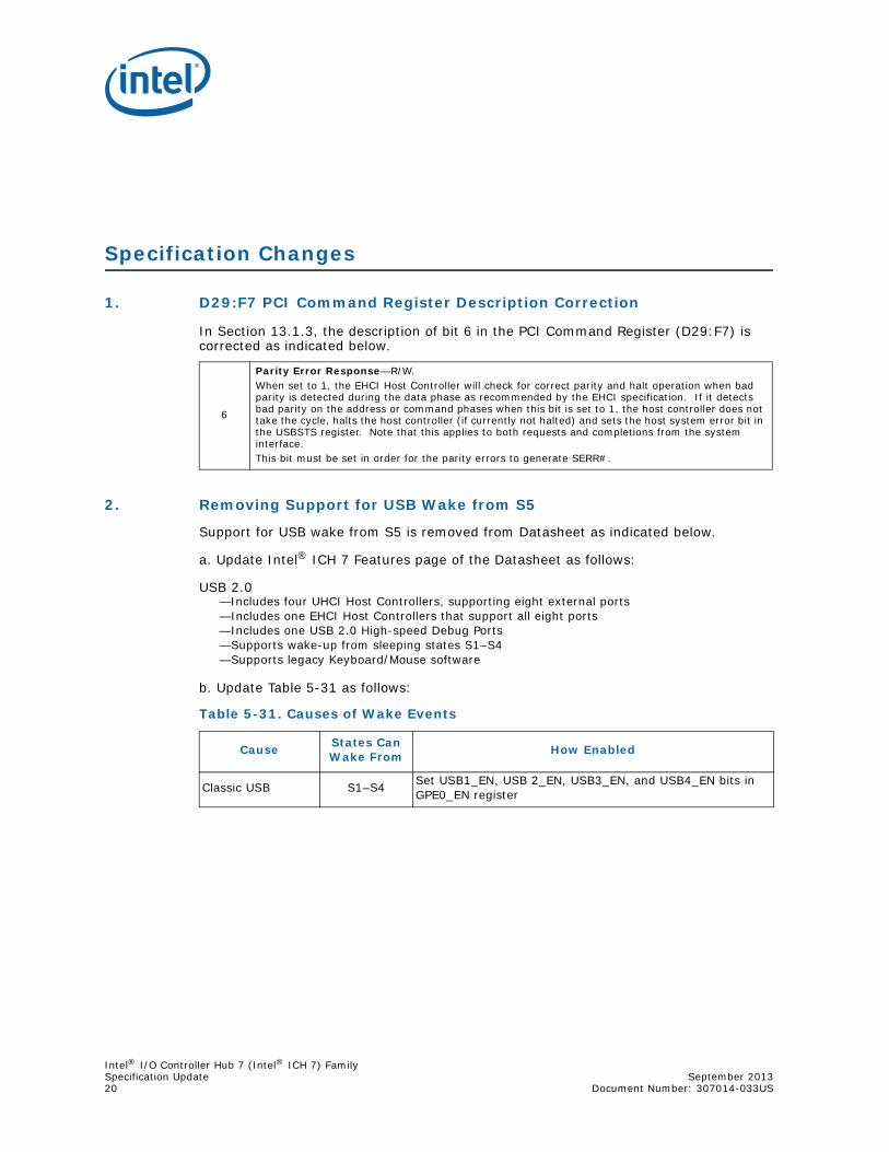
Intel® I/O Controller Hub 7 (Intel® ICH 7) FamilySpecification Update September 201320 Document Number: 307014-033US
Specification Changes
1. D29:F7 PCI Command Register Description Correction
In Section 13.1.3, the description of bit 6 in the PCI Command Register (D29:F7) is corrected as indicated below.
2. Removing Support for USB Wake from S5
Support for USB wake from S5 is removed from Datasheet as indicated below.
a. Update Intel® ICH 7 Features page of the Datasheet as follows:
USB 2.0—Includes four UHCI Host Controllers, supporting eight external ports—Includes one EHCI Host Controllers that support all eight ports—Includes one USB 2.0 High-speed Debug Ports—Supports wake-up from sleeping states S1–S4—Supports legacy Keyboard/Mouse software
b. Update Table 5-31 as follows:
Table 5-31. Causes of Wake Events
6
Parity Error Response—R/W.When set to 1, the EHCI Host Controller will check for correct parity and halt operation when bad parity is detected during the data phase as recommended by the EHCI specification. If it detects bad parity on the address or command phases when this bit is set to 1, the host controller does not take the cycle, halts the host controller (if currently not halted) and sets the host system error bit in the USBSTS register. Note that this applies to both requests and completions from the system interface.This bit must be set in order for the parity errors to generate SERR#.
Cause States Can Wake From How Enabled
Classic USB S1–S4 Set USB1_EN, USB 2_EN, USB3_EN, and USB4_EN bits in GPE0_EN register
Intel® I/O Controller Hub 7 (Intel® ICH 7) FamilySeptember 2013 Specification UpdateDocument Number: 307014-033US 21
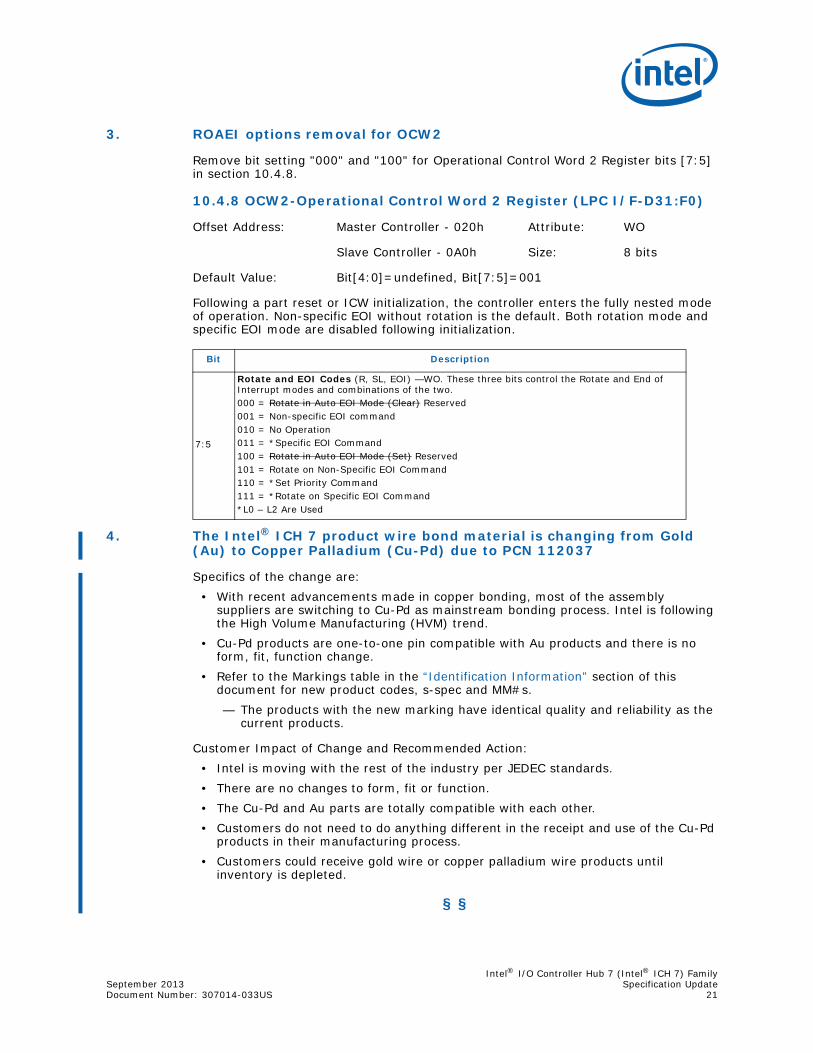
3. ROAEI options removal for OCW2
Remove bit setting "000" and "100" for Operational Control Word 2 Register bits [7:5] in section 10.4.8.
10.4.8 OCW2-Operational Control Word 2 Register (LPC I/F-D31:F0)
Offset Address: Master Controller - 020h Attribute: WO
Slave Controller - 0A0h Size: 8 bits
Default Value: Bit[4:0]=undefined, Bit[7:5]=001
Following a part reset or ICW initialization, the controller enters the fully nested mode of operation. Non-specific EOI without rotation is the default. Both rotation mode and specific EOI mode are disabled following initialization.
4. The Intel® ICH 7 product wire bond material is changing from Gold (Au) to Copper Palladium (Cu-Pd) due to PCN 112037
Specifics of the change are: • With recent advancements made in copper bonding, most of the assembly
suppliers are switching to Cu-Pd as mainstream bonding process. Intel is following the High Volume Manufacturing (HVM) trend.
• Cu-Pd products are one-to-one pin compatible with Au products and there is no form, fit, function change.
• Refer to the Markings table in the “Identification Information” section of this document for new product codes, s-spec and MM#s. — The products with the new marking have identical quality and reliability as the
current products.
Customer Impact of Change and Recommended Action: • Intel is moving with the rest of the industry per JEDEC standards. • There are no changes to form, fit or function. • The Cu-Pd and Au parts are totally compatible with each other. • Customers do not need to do anything different in the receipt and use of the Cu-Pd
products in their manufacturing process. • Customers could receive gold wire or copper palladium wire products until
inventory is depleted.
§ §
Bit Description
7:5
Rotate and EOI Codes (R, SL, EOI) —WO. These three bits control the Rotate and End of Interrupt modes and combinations of the two.000 = Rotate in Auto EOI Mode (Clear) Reserved 001 = Non-specific EOI command 010 = No Operation 011 = *Specific EOI Command 100 = Rotate in Auto EOI Mode (Set) Reserved 101 = Rotate on Non-Specific EOI Command 110 = *Set Priority Command 111 = *Rotate on Specific EOI Command *L0 – L2 Are Used
Intel® I/O Controller Hub 7 (Intel® ICH 7) FamilySpecification Update September 201322 Document Number: 307014-033US
Specification Clarifications
1. t290, t293, and t294 Clarification
Note 14 for t290, t293, and t294 in Table 23-23 of the Datasheet is changed as indicated below:
14. t290, t293, and t294 apply during S0 to S3/S4/S5 and S0 to G3 transitions. In addition, the timings are not applied to V5REF. V5REF timings are bounded by power sequencing.
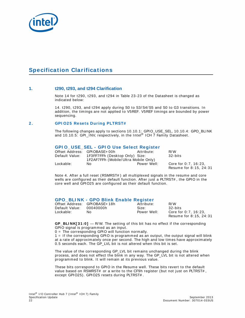
2. GPIO25 Resets During PLTRST#
The following changes apply to sections 10.10.1: GPIO_USE_SEL, 10.10.4: GPO_BLINK and 10.10.5: GPI_INV, respectively, in the Intel® ICH 7 Family Datasheet.
GPIO_USE_SEL - GPIO Use Select RegisterOffset Address: GPIOBASE+00h Attribute: R/WDefault Value: 1F3FF7FFh (Desktop Only) Size: 32-bits
1F2AF7FFh (Mobile/Ultra Mobile Only)Lockable: No Power Well: Core for 0:7, 16:23,
Resume for 8:15, 24:31
Note 4. After a full reset (RSMRST#) all multiplexed signals in the resume and core wells are configured as their default function. After just a PLTRST#, the GPIO in the core well and GPIO25 are configured as their default function.
GPO_BLINK - GPO Blink Enable RegisterOffset Address: GPIOBASE+18h Attribute: R/WDefault Value: 00040000h Size: 32-bitsLockable: No Power Well: Core for 0:7, 16:23,
Resume for 8:15, 24:31
GP_BLINK[31:0] — R/W. The setting of this bit has no effect if the corresponding GPIO signal is programmed as an input.0 = The corresponding GPIO will function normally.1 = If the corresponding GPIO is programmed as an output, the output signal will blink at a rate of approximately once per second. The high and low times have approximately 0.5 seconds each. The GP_LVL bit is not altered when this bit is set.
The value of the corresponding GP_LVL bit remains unchanged during the blink process, and does not effect the blink in any way. The GP_LVL bit is not altered when programmed to blink. It will remain at its previous value.
These bits correspond to GPIO in the Resume well. These bits revert to the default value based on RSMRST# or a write to the CF9h register (but not just on PLTRST#, except GPIO25). GPIO25 resets during PLTRST#.
Intel® I/O Controller Hub 7 (Intel® ICH 7) FamilySeptember 2013 Specification UpdateDocument Number: 307014-033US 23
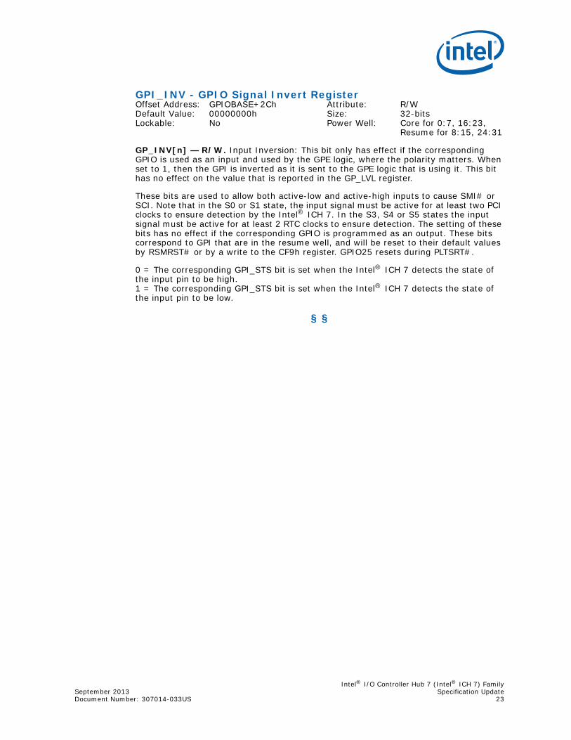
GPI_INV - GPIO Signal Invert RegisterOffset Address: GPIOBASE+2Ch Attribute: R/WDefault Value: 00000000h Size: 32-bitsLockable: No Power Well: Core for 0:7, 16:23,
Resume for 8:15, 24:31
GP_INV[n] — R/W. Input Inversion: This bit only has effect if the corresponding GPIO is used as an input and used by the GPE logic, where the polarity matters. When set to 1, then the GPI is inverted as it is sent to the GPE logic that is using it. This bit has no effect on the value that is reported in the GP_LVL register.
These bits are used to allow both active-low and active-high inputs to cause SMI# or SCI. Note that in the S0 or S1 state, the input signal must be active for at least two PCI clocks to ensure detection by the Intel® ICH 7. In the S3, S4 or S5 states the input signal must be active for at least 2 RTC clocks to ensure detection. The setting of these bits has no effect if the corresponding GPIO is programmed as an output. These bits correspond to GPI that are in the resume well, and will be reset to their default values by RSMRST# or by a write to the CF9h register. GPIO25 resets during PLTSRT#.
0 = The corresponding GPI_STS bit is set when the Intel® ICH 7 detects the state of the input pin to be high.1 = The corresponding GPI_STS bit is set when the Intel® ICH 7 detects the state of the input pin to be low.
§ §
Intel® I/O Controller Hub 7 (Intel® ICH 7) FamilySpecification Update September 201324 Document Number: 307014-033US
Document Changes
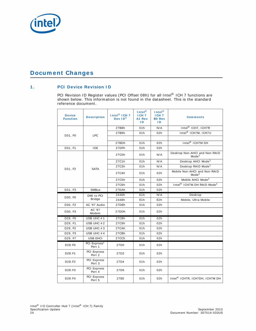
1. PCI Device Revision ID
PCI Revision ID Register values (PCI Offset 08h) for all Intel® ICH 7 functions are shown below. This information is not found in the datasheet. This is the standard reference document.
Device Function Description Intel® ICH 7
Dev ID1
Intel® ICH 7
A1 Rev ID
Intel® ICH 7
B0 Rev ID
Comments
D31, F0 LPC
27B8h 01h N/A Intel® ICH7, ICH7R
27B9h 01h 02h Intel® ICH7M, ICH7U
27BDh 01h 02h Intel® ICH7M DH
D31, F1 IDE 27DFh 01h 02h
D31, F2 SATA
27C0h 01h N/A Desktop Non-AHCI and Non-RAID Mode1
27C1h 01h N/A Desktop AHCI Mode1
27C3h 01h N/A Desktop RAID Mode1
27C4h 01h 02h Mobile Non-AHCI and Non-RAID Mode1
27C5h 01h 02h Mobile AHCI Mode1
27C6h 01h 02h Intel® ICH7M DH RAID Mode1
D31, F3 SMBus 27DAh 01h 02h
D30, F0 DMI to PCI Bridge
244Eh E1h N/A Desktop
2448h E1h E2h Mobile, Ultra Mobile
D30, F2 AC ‘97 Audio 27DEh 01h 02h
D30, F3 AC ‘97 Modem 27DDh 01h 02h
D29, F0 USB UHC #1 27C8h 01h 02h
D29, F1 USB UHC #2 27C9h 01h 02h
D29, F2 USB UHC #3 27CAh 01h 02h
D29, F3 USB UHC #4 27CBh 01h 02h
D29, F7 USB EHCI 27CCh 01h 02h
D28:F0 PCI Express* Port 1 27D0 01h 02h
D28:F1 PCI Express Port 2 27D2 01h 02h
D28:F2 PCI Express Port 3 27D4 01h 02h
D28:F3 PCI Express Port 4 27D6 01h 02h
D28:F4 PCI Express Port 5 27E0 01h 02h Intel® ICH7R, ICH7DH, ICH7M DH
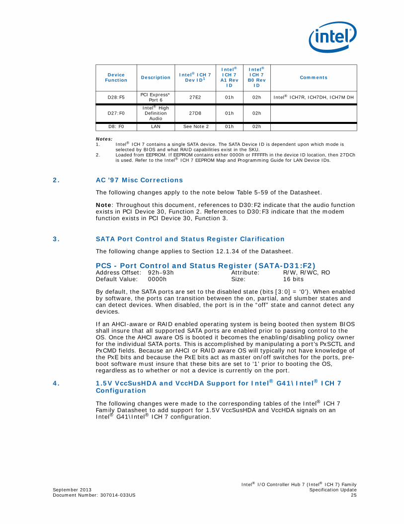
Intel® I/O Controller Hub 7 (Intel® ICH 7) FamilySeptember 2013 Specification UpdateDocument Number: 307014-033US 25
Notes:1. Intel® ICH 7 contains a single SATA device. The SATA Device ID is dependent upon which mode is
selected by BIOS and what RAID capabilities exist in the SKU.2. Loaded from EEPROM. If EEPROM contains either 0000h or FFFFFh in the device ID location, then 27DCh
is used. Refer to the Intel® ICH 7 EEPROM Map and Programming Guide for LAN Device IDs.
2. AC ’97 Misc Corrections
The following changes apply to the note below Table 5-59 of the Datasheet.
Note: Throughout this document, references to D30:F2 indicate that the audio function exists in PCI Device 30, Function 2. References to D30:F3 indicate that the modem function exists in PCI Device 30, Function 3.
3. SATA Port Control and Status Register Clarification
The following change applies to Section 12.1.34 of the Datasheet.
PCS - Port Control and Status Register (SATA-D31:F2)Address Offset: 92h–93h Attribute: R/W, R/WC, RODefault Value: 0000h Size: 16 bits
By default, the SATA ports are set to the disabled state (bits [3:0] = ‘0’). When enabled by software, the ports can transition between the on, partial, and slumber states and can detect devices. When disabled, the port is in the “off” state and cannot detect any devices.
If an AHCI-aware or RAID enabled operating system is being booted then system BIOS shall insure that all supported SATA ports are enabled prior to passing control to the OS. Once the AHCI aware OS is booted it becomes the enabling/disabling policy owner for the individual SATA ports. This is accomplished by manipulating a port’s PxSCTL and PxCMD fields. Because an AHCI or RAID aware OS will typically not have knowledge of the PxE bits and because the PxE bits act as master on/off switches for the ports, pre-boot software must insure that these bits are set to ‘1’ prior to booting the OS, regardless as to whether or not a device is currently on the port.
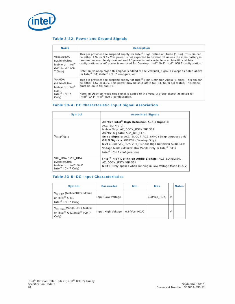
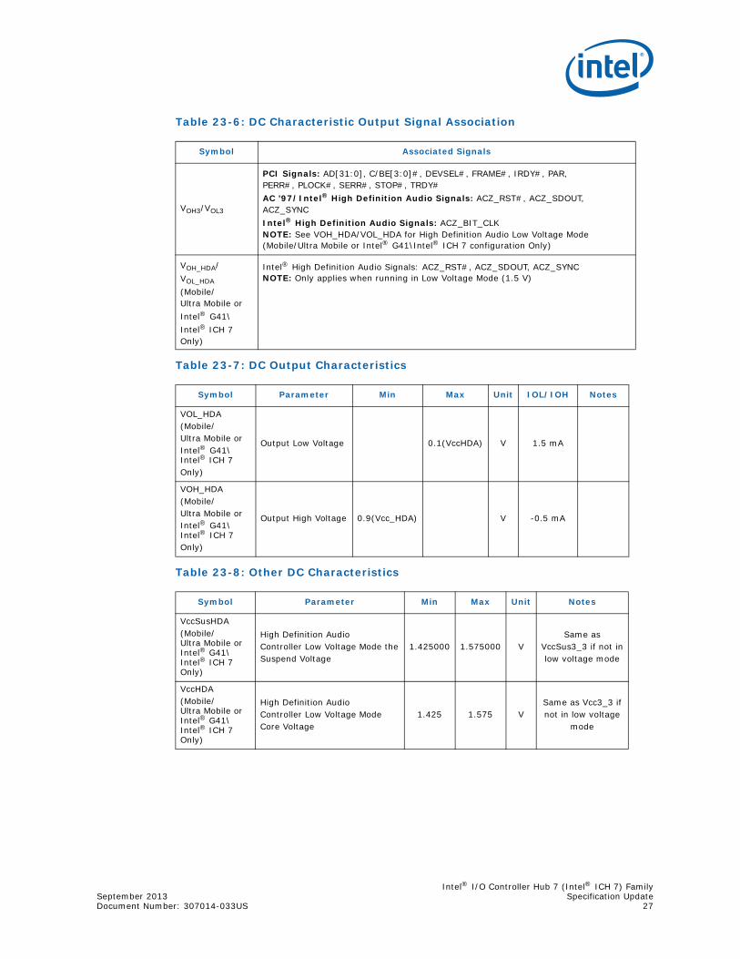
4. 1.5V VccSusHDA and VccHDA Support for Intel® G41\Intel® ICH 7 Configuration
The following changes were made to the corresponding tables of the Intel® ICH 7 Family Datasheet to add support for 1.5V VccSusHDA and VccHDA signals on an Intel® G41\Intel® ICH 7 configuration.
D28:F5 PCI Express* Port 6 27E2 01h 02h Intel® ICH7R, ICH7DH, ICH7M DH
D27:F0Intel® High Definition
Audio27D8 01h 02h
D8: F0 LAN See Note 2 01h 02h
Device Function Description Intel® ICH 7
Dev ID1
Intel® ICH 7
A1 Rev ID
Intel® ICH 7
B0 Rev ID
Comments
Intel® I/O Controller Hub 7 (Intel® ICH 7) FamilySpecification Update September 201326 Document Number: 307014-033US
Table 2-22: Power and Ground Signals
Table 23-4: DC Characteristic Input Signal Association
Table 23-5: DC Input Characteristics
Name Description
VccSusHDA(Mobile/UltraMobile or Intel®
G41\Intel® ICH 7 Only)
This pin provides the suspend supply for Intel® High Definition Audio (1 pin). This pin can be either 1.5v or 3.3v.This power is not expected to be shut off unless the main battery is removed or completely drained and AC power is not available in mobile Ultra Mobile configurations or AC power is removed for Desktop Intel® G41\Intel® ICH 7 configuration.
Note: In Desktop mode this signal is added to the VccSus3_3 group except as noted above for Intel® G41\Intel® ICH 7 configuration.
VccHDA(Mobile/UltraMobile or Intel®
G41\Intel® ICH 7 Only)
This pin provides the suspend supply for Intel® High Definition Audio (1 pins). This pin can be either 1.5v or 3.3v. This power may be shut off in S3, S4, S5 or G3 states. This plane must be on in S0 and S1.
Note: In Desktop mode this signal is added to the Vcc3_3 group except as noted for Intel® G41\Intel® ICH 7 configuration.
Symbol Associated Signals
VIH11/VIL11
AC ’97/Intel® High Definition Audio Signals: ACZ_SDIN[2:0],Mobile Only: AZ_DOCK_RST#/GPIO34AC ‘97 Signals: ACZ_BIT_CLKStrap Signals: ACZ_SDOUT, ACZ_SYNC (Strap purposes only)GPIO Signals: GPIO34 (Desktop Only)NOTE: See VIL_HDA/VIH_HDA for High Definition Audio Low Voltage Mode (Mobile/Ultra Mobile Only or Intel® G41\Intel® ICH 7 configuration)
VIH_HDA / VIL_HDA(Mobile/UltraMobile or Intel® G41\Intel® ICH 7 Only)
Intel® High Definition Audio Signals: ACZ_SDIN[2:0],AZ_DOCK_RST#/GPIO34NOTE: Only applies when running in Low Voltage Mode (1.5 V)
Symbol Parameter Min Max Notes
VIL_HDA (Mobile/Ultra Mobile
or Intel® G41\Intel® ICH 7 Only)
Input Low Voltage 0.4(Vcc_HDA) V
VIH_HDA(Mobile/Ultra Mobile
or Intel® G41\Intel® ICH 7 Only)
Input High Voltage 0.6(Vcc_HDA) V
Intel® I/O Controller Hub 7 (Intel® ICH 7) FamilySeptember 2013 Specification UpdateDocument Number: 307014-033US 27
Table 23-6: DC Characteristic Output Signal Association
Table 23-7: DC Output Characteristics
Table 23-8: Other DC Characteristics
Symbol Associated Signals
VOH3/VOL3
PCI Signals: AD[31:0], C/BE[3:0]#, DEVSEL#, FRAME#, IRDY#, PAR,PERR#, PLOCK#, SERR#, STOP#, TRDY#AC ’97/Intel® High Definition Audio Signals: ACZ_RST#, ACZ_SDOUT,ACZ_SYNCIntel® High Definition Audio Signals: ACZ_BIT_CLKNOTE: See VOH_HDA/VOL_HDA for High Definition Audio Low Voltage Mode(Mobile/Ultra Mobile or Intel® G41\Intel® ICH 7 configuration Only)
VOH_HDA/VOL_HDA(Mobile/Ultra Mobile or Intel® G41\Intel® ICH 7 Only)
Intel® High Definition Audio Signals: ACZ_RST#, ACZ_SDOUT, ACZ_SYNCNOTE: Only applies when running in Low Voltage Mode (1.5 V)
Symbol Parameter Min Max Unit IOL/IOH Notes
VOL_HDA(Mobile/Ultra Mobile or Intel® G41\Intel® ICH 7 Only)
Output Low Voltage 0.1(VccHDA) V 1.5 mA
VOH_HDA (Mobile/Ultra Mobile or Intel® G41\ Intel® ICH 7 Only)
Output High Voltage 0.9(Vcc_HDA) V -0.5 mA
Symbol Parameter Min Max Unit Notes
VccSusHDA(Mobile/Ultra Mobile or Intel® G41\Intel® ICH 7 Only)
High Definition AudioController Low Voltage Mode theSuspend Voltage
1.425000 1.575000 VSame as
VccSus3_3 if not inlow voltage mode
VccHDA(Mobile/Ultra Mobile or Intel® G41\Intel® ICH 7 Only)
High Definition AudioController Low Voltage ModeCore Voltage
1.425 1.575 VSame as Vcc3_3 ifnot in low voltage
mode
Intel® I/O Controller Hub 7 (Intel® ICH 7) FamilySpecification Update September 201328 Document Number: 307014-033US
5. Correct section 5.14.7.5 Sx-G3-Sx, Handling Power Failures regarding possible wake events following a power failure
Correct section 5.14.7.5 Sx-G3-Sx, Handling Power Failures in the Datasheet.
Section 5.14.7.5 Sx-G3-Xs, Handling Power Failures
Depending on when the power failure occurs and how the system is designed, different transitions could occur due to a power failure.
The AFTER_G3 bit provides the ability to program whether or not the system should boot once power returns after a power loss event. If the policy is to not boot, the system remains in an S5 state (unless previously in S4). There are only three possible events that will wake the system after a power failure. The following wake events can wake the system following a power loss by either RSMRST# going low and enabling by default, the enable bits reside in the RCT well or the wake event is always enabled.
1.PWRBTN#: PWRBTN# is always enabled as a wake event. When RSMRST# is low (G3 state), the PWRBTN_STS bit is reset. When the Intel® ICH 7 exits G3 after power returns (RSMRST# goes high), the PWRBTN# signal is already high (because VCC-standby goes high before RSMRST# goes high) and the PWRBTN_STS bit is 0.
2.RI#: RI# does not have an internal pull-up. Therefore, if this signal is enabled as a wake event, it is important to keep this signal powered during the power loss event. If this signal goes low (active), when power returns the RI_STS bit is set and the system interprets that as a wake event.
3.RTC Alarm: The RTC_EN bit is in the RTC well and is preserved after a power loss. Like PWRBTN_STS the RTC_STS bit is cleared when RSMRST# goes low.
4.PCI Express* Wake# Signal: The PCIEXPWAK_DIS bit is cleared by RSMRST#going low enabling PCI Express Ports to wake the platform after a power loss. ThePCIEXPWAK_STS bit is also cleared when RSMRST# goes low.
5.PME_B0: PME_B0_EN is in the RTC Well and is preserved after a power loss. The PME_B0_STS bit is also cleared when RSMRST# goes low.
6.PME: PME_EN: is in the RTC Well and is preserved after a power loss. The PME_STS bit is also cleared when RSMRST# goes low.
7.Host SMBUS: SMBALERT# or Slave Wake message is always enabled as Wake Event
The Intel® ICH 7 monitors both PWROK and RSMRST# to detect for power failures. If PWROK goes low, the PWROK_FLR bit is set. If RSMRST# goes low, PWR_FLR is set.
Note: Although PME_EN is in the RTC well, this signal cannot wake the system after a power loss. PME_EN is cleared by RTCRST#, and PME_STS is cleared by RSMRST#.
Intel® I/O Controller Hub 7 (Intel® ICH 7) FamilySeptember 2013 Specification UpdateDocument Number: 307014-033US 29
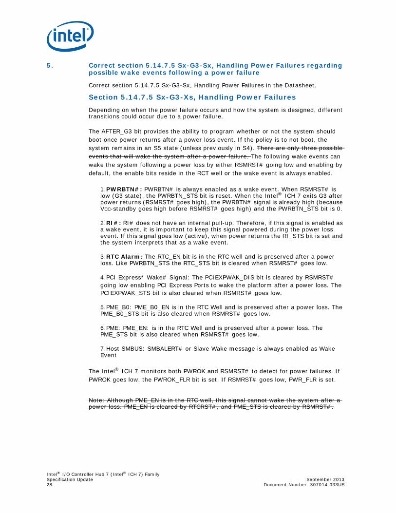
6. Remove t217 timing from Figure 23-21
Remove t217 timing that points from VRMPWRGD going high to SUS_STAT# going high from Figure 23-21: G3 (Mechanical Off) to S0 Timings (Mobile/Ultra Mobile Only) in the Datasheet.
Figure 23-21: G3 (Mechanical Off) to S0 Timings (Mobile/Ultra Mobile Only)
SLP_S3#
Vcc1, VccLAN
PWROK, LAN_RST#
SUS_STAT#
PLTRST#
Processor I/F Signals
STPCLK#, STP_CPU#, STP_PCI#, DPSLP#,
DPRSTP#
DMI message
System State
Running
Strap ValuesNormal
Operation
t205
t217
t218
t230
t231
t216
S3 S0 S0 stateG3 S5 S4
t232
t233t234
t214
Main BatteryRemoved (G3)
VccSus1_05
SUSCLK
RSMRST#
SLP_S4#
SLP_S5#
ICH7 G3 t S0 M bil d
VccSus3_3 t202
VRMPWRGDt217
Intel® I/O Controller Hub 7 (Intel® ICH 7) FamilySpecification Update September 201330 Document Number: 307014-033US
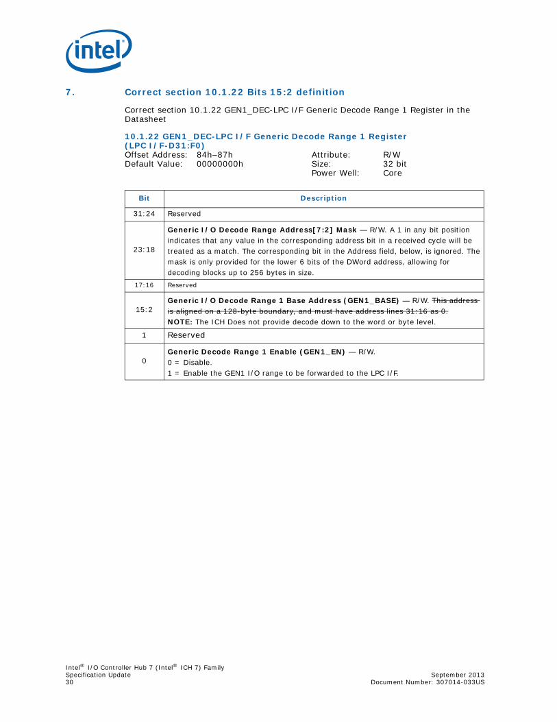
7. Correct section 10.1.22 Bits 15:2 definition
Correct section 10.1.22 GEN1_DEC-LPC I/F Generic Decode Range 1 Register in the Datasheet
10.1.22 GEN1_DEC-LPC I/F Generic Decode Range 1 Register (LPC I/F-D31:F0)Offset Address: 84h–87h Attribute: R/WDefault Value: 00000000h Size: 32 bit
Power Well: Core
Bit Description
31:24 Reserved
23:18
Generic I/O Decode Range Address[7:2] Mask — R/W. A 1 in any bit positionindicates that any value in the corresponding address bit in a received cycle will betreated as a match. The corresponding bit in the Address field, below, is ignored. Themask is only provided for the lower 6 bits of the DWord address, allowing for decoding blocks up to 256 bytes in size.
17:16 Reserved
15:2Generic I/O Decode Range 1 Base Address (GEN1_BASE) — R/W. This address is aligned on a 128-byte boundary, and must have address lines 31:16 as 0.NOTE: The ICH Does not provide decode down to the word or byte level.
1 Reserved
0Generic Decode Range 1 Enable (GEN1_EN) — R/W.0 = Disable.1 = Enable the GEN1 I/O range to be forwarded to the LPC I/F.
Intel® I/O Controller Hub 7 (Intel® ICH 7) FamilySeptember 2013 Specification UpdateDocument Number: 307014-033US 31
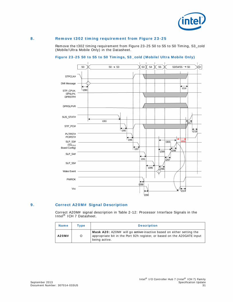
8. Remove t302 timing requirement from Figure 23-25
Remove the t302 timing requirement from Figure 23-25 S0 to S5 to S0 Timing, S3_cold (Mobile/Ultra Mobile Only) in the Datasheet.
Figure 23-25 S0 to S5 to S0 Timings, S3_cold (Mobile/Ultra Mobile Only)
9. Correct A20M# Signal Description
Correct A20M# signal description in Table 2-12: Processor Interface Signals in the Intel® ICH 7 Datasheet.
STP_CPU#, DPSLP#,
DPRSTP#
PLTRST#PCIRST#
SLP_S3#(S3COLD
Board Config)
SLP_S5#
Wake Event
PWROK
Vcc
S0 S0 S3 S3 S5 S3/S4/S5 S0 S0
t295
t288
t290
t296
t214
t217
t218
STP_PCI#
STPCLK#
DMI Message
DPRSLPVR
t280
t283
t285
t287
t286
SUS_STAT#
S4
SLP_S4#
t291 t297
t300
t298
t216
t299
t302
Name Type Description
A20M# OMask A20: A20M# will go active inactive based on either setting the appropriate bit in the Port 92h register, or based on the A20GATE input being active.
Intel® I/O Controller Hub 7 (Intel® ICH 7) FamilySpecification Update September 201332 Document Number: 307014-033US
10. Update Section 8.2 in the Datasheet
The title of section 8.2 of the Intel® ICH 7 Datasheet is changed as below.
8.2 Absolute Maximum and Minimum Ratings
The following paragraphs are added to section 8.2:
Table 8-1 specifies absolute maximum and minimum ratings. At conditions outside functional operation condition limits, but within absolute maximum and minimum ratings, neither functionality nor long-term reliability can be expected. If a device is returned to conditions within functional operation limits after having been subjected to conditions outside these limits (but within the absolute maximum and minimum ratings) the device may be functional, but with its lifetime degraded depending on exposure to conditions exceeding the functional operation condition limits.
At conditions exceeding absolute maximum and minimum ratings, neither functionality nor long-term reliability can be expected. Moreover, if a device is subjected to these conditions for any length of time, it will either not function or its reliability will be severely degraded when returned to conditions within the functional operating condition limits.
Although the Intel® ICH 7 contains protective circuitry to resist damage from Electro-Static Discharge (ESD), precautions should always be taken to avoid high static voltages or electric fields.
Intel® I/O Controller Hub 7 (Intel® ICH 7) FamilySeptember 2013 Specification UpdateDocument Number: 307014-033US 33
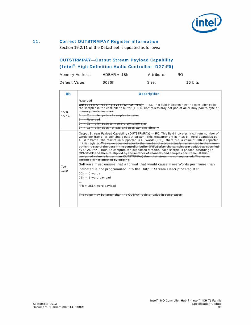
11. Correct OUTSTRMPAY Register informationSection 19.2.11 of the Datasheet is updated as follows:
OUTSTRMPAY—Output Stream Payload Capability(Intel® High Definition Audio Controller—D27:F0)
Memory Address: HDBAR + 18h Attribute: RO
Default Value: 0030h Size: 16 bits
Bit Description
15:815:14
ReservedOutput FIFO Padding Type (OPADTYPE) — RO. This field indicates how the controller pads the samples in the controller's buffer (FIFO). Controllers may not pad at all or may pad to byte or memory container sizes.0h = Controller pads all samples to bytes1h = Reserved2h = Controller pads to memory container size3h = Controller does not pad and uses samples directly
7:013:0
Output Stream Payload Capability (OUTSTRMPAY) — RO. This field indicates maximum number of words per frame for any single output stream. This measurement is in 16 bit word quantities per 48 kHz frame. The maximum supported is 48 Words (96B); therefore, a value of 30h is reported in this register. The value does not specify the number of words actually transmitted in the frame, but is the size of the data in the controller buffer (FIFO) after the samples are padded as specified by OPADTYPE. Thus, to compute the supported streams, each sample is padded according to OPADTYPE and then multiplied by the number of channels and samples per frame. If this computed value is larger than OUTSTRMPAY, then that stream is not supported. The value specified is not affected by striping.Software must ensure that a format that would cause more Words per frame thanindicated is not programmed into the Output Stream Descriptor Register.00h = 0 words01h = 1 word payload…FFh = 255h word payload
The value may be larger than the OUTPAY register value in some cases.
Intel® I/O Controller Hub 7 (Intel® ICH 7) FamilySpecification Update September 201334 Document Number: 307014-033US
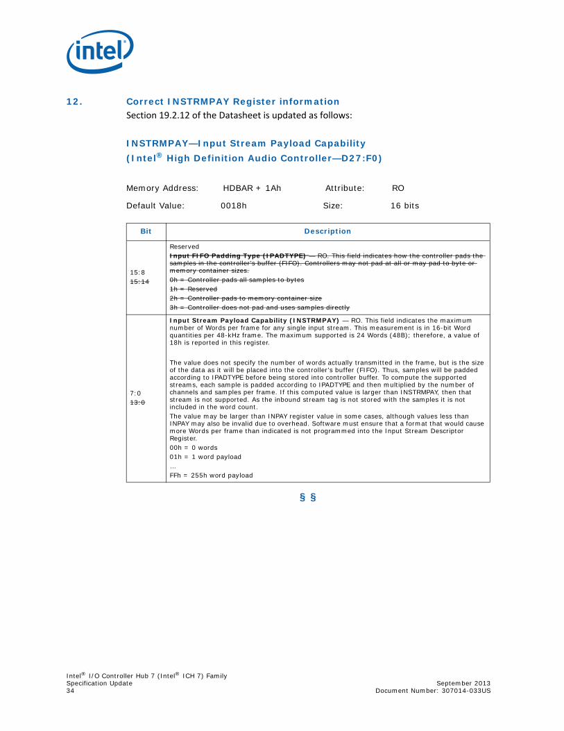
12. Correct INSTRMPAY Register informationSection 19.2.12 of the Datasheet is updated as follows:
INSTRMPAY—Input Stream Payload Capability(Intel® High Definition Audio Controller—D27:F0)
Memory Address: HDBAR + 1Ah Attribute: RO
Default Value: 0018h Size: 16 bits
§ §
Bit Description
15:815:14
ReservedInput FIFO Padding Type (IPADTYPE) — RO. This field indicates how the controller pads the samples in the controller's buffer (FIFO). Controllers may not pad at all or may pad to byte or memory container sizes.0h = Controller pads all samples to bytes1h = Reserved2h = Controller pads to memory container size3h = Controller does not pad and uses samples directly
7:013:0
Input Stream Payload Capability (INSTRMPAY) — RO. This field indicates the maximum number of Words per frame for any single input stream. This measurement is in 16-bit Word quantities per 48-kHz frame. The maximum supported is 24 Words (48B); therefore, a value of 18h is reported in this register.
The value does not specify the number of words actually transmitted in the frame, but is the size of the data as it will be placed into the controller's buffer (FIFO). Thus, samples will be padded according to IPADTYPE before being stored into controller buffer. To compute the supported streams, each sample is padded according to IPADTYPE and then multiplied by the number of channels and samples per frame. If this computed value is larger than INSTRMPAY, then that stream is not supported. As the inbound stream tag is not stored with the samples it is not included in the word count.The value may be larger than INPAY register value in some cases, although values less than INPAY may also be invalid due to overhead. Software must ensure that a format that would cause more Words per frame than indicated is not programmed into the Input Stream Descriptor Register.00h = 0 words01h = 1 word payload…FFh = 255h word payload