Intel® E8501 Chipset North Bridge (NB) · 2 Intel® E8501 Chipset North Bridge (NB) Datasheet...
388
Intel® E8501 Chipset North Bridge (NB) Datasheet May 2006 Document Number: 309620-001
Transcript of Intel® E8501 Chipset North Bridge (NB) · 2 Intel® E8501 Chipset North Bridge (NB) Datasheet...
Intel® E8501 Chipset North Bridge (NB)Datasheet
May 2006
Document Number: 309620-001
2 Intel® E8501 Chipset North Bridge (NB) Datasheet
INFORMATION IN THIS DOCUMENT IS PROVIDED IN CONNECTION WITH INTEL® PRODUCTS. NO LICENSE, EXPRESS OR IMPLIED, BY ESTOPPEL OR OTHERWISE, TO ANY INTELLECTUAL PROPERTY RIGHTS IS GRANTED BY THIS DOCUMENT. EXCEPT AS PROVIDED IN INTEL'S TERMS AND CONDITIONS OF SALE FOR SUCH PRODUCTS, INTEL ASSUMES NO LIABILITY WHATSOEVER, AND INTEL DISCLAIMS ANY EXPRESS OR IMPLIED WARRANTY, RELATING TO SALE AND/OR USE OF INTEL PRODUCTS INCLUDING LIABILITY OR WARRANTIES RELATING TO FITNESS FOR A PARTICULAR PURPOSE, MERCHANTABILITY, OR INFRINGEMENT OF ANY PATENT, COPYRIGHT OR OTHER INTELLECTUAL PROPERTY RIGHT. Intel products are not intended for use in medical, life saving, or life sustaining applications.
Intel may make changes to specifications and product descriptions at any time, without notice.
Designers must not rely on the absence or characteristics of any features or instructions marked “reserved” or “undefined.” Intel reserves these for future definition and shall have no responsibility whatsoever for conflicts or incompatibilities arising from future changes to them.
The Intel® E8501 Chipset North Bridge (NB) may contain design defects or errors known as errata which may cause the product to deviate from published specifications. Current characterized errata are available on request.
Contact your local Intel sales office or your distributor to obtain the latest specifications and before placing your product order.
I2C is a two-wire communications bus/protocol developed by Phillips. SMBus is a subset of the I2C bus/protocol and was developed by Intel. Implementations of the I2C bus/protocol may require licenses from various entities, including Phillips Electronics N.V. and North American Phillips Corporation.
Intel and the Intel logo are trademarks or registered trademarks of Intel Corporation or its subsidiaries in the United States and other countries.
*Other names and brands may be claimed as the property of others.
Copyright © 2006, Intel Corporation.
Intel® E8501 Chipset North Bridge (NB) Datasheet 3
Contents1 Introduction.......................................................................................................................17
1.1 Intel® E8501 Chipset North Bridge (NB) Feature List .........................................181.1.1 Processor Front Side Bus Support.........................................................181.1.2 Independent Memory Interface ..............................................................181.1.3 I/O Interfaces..........................................................................................181.1.4 Transaction Processing Capabilities ......................................................191.1.5 RASUM ..................................................................................................191.1.6 Package .................................................................................................19
1.2 Intel® E8501 Chipset eXternal Memory Bridge (XMB) Feature List ....................201.2.1 DDR Memory Support ............................................................................201.2.2 IMI Support.............................................................................................201.2.3 RASUM Features ...................................................................................201.2.4 Intel® E8501 Chipset eXternal Memory Bridge (XMB) Package ............21
1.3 Terminology.........................................................................................................211.4 References ..........................................................................................................26
2 Overview ..........................................................................................................................272.1 Logical Pin Grouping ...........................................................................................272.2 Quadrant Placement ...........................................................................................292.3 Register Devices .................................................................................................292.4 Intel® E8501 Chipset North Bridge (NB) Clocking ..............................................312.5 Interrupt Delivery .................................................................................................31
2.5.1 xAPIC Interrupt Message Delivery .........................................................322.6 Intel® E8501 Chipset North Bridge (NB) RAS Features......................................33
2.6.1 Data Integrity (Error Detection) ..............................................................332.6.2 Error Reporting.......................................................................................342.6.3 Memory Mirroring ...................................................................................352.6.4 Memory RAID.........................................................................................352.6.5 Hot-Plug .................................................................................................35
3 Signal Description ............................................................................................................373.1 Conventions ........................................................................................................373.2 FSB Signals.........................................................................................................383.3 Independent Memory Interface (IMI) Signals ......................................................403.4 PCI Express Ports Signals ..................................................................................41
3.4.1 Industry Standard Naming Convention ..................................................423.5 Hub Interface 1.5 (HI1.5) Signals ........................................................................453.6 Clocking and Analog Power Signals ...................................................................453.7 Reset Signals ......................................................................................................473.8 Debug Signals .....................................................................................................473.9 RAS Signal ..........................................................................................................483.10 Miscellaneous Signals.........................................................................................49
4 Register Description .........................................................................................................514.1 Register Terminology ..........................................................................................51
4 Intel® E8501 Chipset North Bridge (NB) Datasheet
4.2 Platform Configuration ........................................................................................ 524.3 Conflict Resolution and Usage Model Limitations............................................... 524.4 Device Mapping .................................................................................................. 534.5 Allowable Configuration Access.......................................................................... 554.6 I/O Mapped Registers ......................................................................................... 56
4.6.1 CFGADR –Configuration Address Register ........................................... 564.6.2 CFGDAT –Configuration Data Register ................................................. 57
4.7 Intel® E8501 Chipset North Bridge (NB) Fixed Mapped Registers ..................... 574.8 PCI Express Device Configuration Registers...................................................... 584.9 Configuration Space Map.................................................................................... 604.10 Hub Interface 1.5 (Device 0, Function 0) ............................................................ 72
4.10.1 VID: Vendor Identification Register (D0, F0) .......................................... 724.10.2 DID: Device Identification Register (D0, F0) .......................................... 724.10.3 PCICMD:PCI Command Register (D0, F0) ............................................ 734.10.4 PCISTS: PCI Status Register (D0, F0)................................................... 734.10.5 RID: Revision Identification Register (D0, F0)........................................ 744.10.6 CCR: Class Code Register (D0, F0) ...................................................... 754.10.7 HDR: Header Type Register (D0, F0) .................................................... 764.10.8 SVID: Subsystem Vendor Identification Register (D0, F0)..................... 764.10.9 SID: Subsystem Identity (D0, F0)........................................................... 764.10.10 HIFERR: Hub Interface First Fatal Error Register (D0, F0).................... 774.10.11 HINERR: Hub Interface Next Fatal Error Register (D0, F0) ................... 774.10.12 NRECHI: Non-Recoverable Hub Interface Error Log
Register (D0, F0).................................................................................... 784.10.13 RECHI: Recoverable Hub Interface Error Log Register (D0, F0)........... 804.10.14 HIEMASK: Hub Interface Error Mask Register (D0, F0) ........................ 814.10.15 HIERR0: Hub Interface Error 0 Mask Register (D0, F0) ........................ 824.10.16 HIERR1: Hub Interface Error 1 Mask Register (D0, F0) ........................ 834.10.17 HIERR2: Hub Interface Error 2 Mask Register (D0, F0) ........................ 834.10.18 HIMCERR: Hub Interface MCERR Mask Register (D0, F0)................... 844.10.19 HICTL: Hub Interface Command Control Register (D0, F0)................... 844.10.20 HICTL2: Hub Interface Command Control Register (D0, F0)................. 86
4.11 PCI Express Ports (Device 1 - 7, Function 0) ..................................................... 864.11.1 VID[7:1]: Vendor Identification Register (D1-7, F0)................................ 864.11.2 DID[7:1]: Device Identification Register (D1-7, F0) ................................ 864.11.3 EXP_CMD[7:1]: Command Register (D1-7, F0)..................................... 874.11.4 EXP_STS[7:1]: Status Register (D1-7, F0) ............................................ 894.11.5 RID[7:1]: Revision Identification Register (D1-7, F0) ............................. 904.11.6 CCR[7:1]: Class Code Register (D1-7, F0) ............................................ 914.11.7 CLS[7:1]: Cache Line Size (D1-7, F0).................................................... 914.11.8 PRI_LT[7:1]: Primary Latency Timer (D1-7, F0)..................................... 914.11.9 HDR[7:1]: Header Type Register (D1-7, F0) .......................................... 924.11.10 BIST[7:1]: Built-In Self Test (D1-7, F0)................................................... 924.11.11 PBUSN[7:1]: Primary Bus Number (D1-7, F0) ....................................... 924.11.12 SBUSN[7:1]: Secondary Bus Number (D1-7, F0) .................................. 934.11.13 SUBUSN[7:1]: Subordinate Bus Number (D1-7, F0).............................. 934.11.14 SEC_LT[7:1]: Secondary Latency Timer (D1-7, F0) .............................. 934.11.15 IOBASE[7:1]: I/O Base Register (D1-7, F0) ........................................... 94
Intel® E8501 Chipset North Bridge (NB) Datasheet 5
4.11.16 IOLIM[7:1]: I/O Limit Register (D1-7, F0) ...............................................944.11.17 SECSTS[7:1]: Secondary Status (D1-7, F0) ..........................................954.11.18 MBASE[7:1]: Memory Base (D1-7, F0) ..................................................964.11.19 MLIMIT[7:1]: Memory Limit (D1-7, F0) ...................................................964.11.20 PMBASE[7:1]: Prefetchable Memory Base (D1-7, F0)...........................974.11.21 PMLIMIT[7:1]: Prefetchable Memory Limit (D1-7, F0)............................984.11.22 PMBU[7:1]: Prefetchable Memory Base (Upper 32 bits)
(D1-7, F0) ...............................................................................................984.11.23 PMLU[7:1]: Prefetchable Memory Limit (Upper 32 Limit)
(D1-7, F0) ...............................................................................................994.11.24 CAPPTR[7:1]: Capability Pointer (D1-7, F0) ..........................................994.11.25 INTL[7:1]: Interrupt Line Register (D1-7, F0)..........................................994.11.26 INTP[7:1]: Interrupt Pin Register (D1-7, F0).........................................1004.11.27 BCTRL[7:1]: Bridge Control Register (D1-7, F0) ..................................1004.11.28 EXP_CTRL[7:1]: PCI Express Control Register (D1-7, F0) .................1024.11.29 EXP_CTRL2: PCI Express Control Register 2 (D1-7, F0) ...................1054.11.30 PMCAP[7:1]: Power Management Capabilities Register
(D1-7, F0) .............................................................................................1054.11.31 PMSCR[7:1]: Power Management Status and Control
Register (D1-7, F0)...............................................................................1064.11.32 MSICAPID[7:1]: MSI Capability ID (D1-7, F0) ......................................1074.11.33 MSINXPTR[7:1]: MSI Next Pointer (D1-7, F0) .....................................1074.11.34 MSICTRL[7:1]: Message Control Register (D1-7, F0)..........................1074.11.35 MSIAR[7:1]: MSI Address Register (D1-7, F0).....................................1084.11.36 MSIDR[7:1]: MSI Data Register (D1-7, F0) ..........................................1094.11.37 EXP_CAPL[7:1]: PCI Express Capability List Register (D1-7, F0).......1104.11.38 EXP_CAP[7:1]: PCI Express Capabilities Register (D1-7, F0) ............1114.11.39 EXP_DEVCAP[7:1]: PCI Express Device Capabilities
Register (D1-7, F0)...............................................................................1114.11.40 EXP_DEVCTRL[7:1]: PCI Express Device Control Register
(D1-7, F0) .............................................................................................1144.11.41 EXP_DEVSTS[7:1]: PCI Express Device Status Register
(D1-7, F0) .............................................................................................1174.11.42 EXP_LNKCAP[7:1]: PCI Express Link Capabilities Register
(D1-7, F0) .............................................................................................1184.11.43 EXP_LNKCTRL[7:1]: PCI Express Link Control Register
(D1-7, F0) .............................................................................................1204.11.44 EXP_LNKLSTS[7:1]: PCI Express Link Status Register (D1-7, F0).....1214.11.45 EXP_SLOTCAP[7:1]: PCI Express Slot Capabilities Register
(D1-7, F0) .............................................................................................1224.11.46 EXP_SLOTCTRL[7:1]: PCI EXPRESS Slot Control Register
(D1-7, F0) .............................................................................................1244.11.47 EXP_SLOTSTS[7:1]: PCI Express Slot Status Register
(D1-7, F0) .............................................................................................1264.11.48 EXP_RTCTRL[7:1]: PCI Express Root Control Register
(D1-7, F0) .............................................................................................1284.11.49 EXP_RTSTS[7:1]: PCI Express Root Status Register (D1-7, F0)........129
4.12 PCI Express Advanced Function (Device 1 - 7, Function 0) .............................129
6 Intel® E8501 Chipset North Bridge (NB) Datasheet
4.12.1 ENHCAPSTS: Enhanced Advanced Error Reporting Capability Structure (D1-7, F0)............................................................. 130
4.12.2 UNCERRSTS: Uncorrectable Error Status (D1-7, F0) ......................... 1304.12.3 UNCERRMSK: Uncorrectable Error Mask (D1-7, F0).......................... 1314.12.4 UNCERRSEV: Uncorrectable Error Severity (D1-7, F0) ...................... 1324.12.5 CORERRSTS: Correctable Error Status (D1-7, F0)............................. 1334.12.6 CORERRMSK: Correctable Error Mask (D1-7, F0) ............................. 1334.12.7 AERCACR: Advanced Error Capabilities and Control
Register (D1-7, F0) .............................................................................. 1344.12.8 HDRLOG0: Header Log 0 (D1-7, F0)................................................... 1344.12.9 HDRLOG1: Header Log 1 (D1-7, F0)................................................... 1354.12.10 HDRLOG2: Header Log 2 (D1-7, F0)................................................... 1354.12.11 HDRLOG3: Header Log 3 (D1-7, F0)................................................... 1354.12.12 RPERRCMD: Root Port Error Command (D1-7, F0) ........................... 1364.12.13 RPERRMSGSTS: Root Port Error Message Status
(D1-7, F0) ............................................................................................. 1364.12.14 ERRSID: Error Source ID (D1-7, F0) ................................................... 1374.12.15 NBSPCAPID: NB Specific Capability ID (D1-7, F0) ............................. 1374.12.16 EXP_unitERR: PCI Express Unit Error Register (D1-7, F0)................. 1374.12.17 EXP_ERR_DOCMD: PCI Express Error Do Command
Register (D1-7, F0) .............................................................................. 1384.12.18 UNCEDMASK: Uncorrectable Error Detect Mask (D1-7, F0)............... 1404.12.19 COREDMASK: Correctable Error Detect Mask (D1-7, F0) .................. 1414.12.20 RPEDMASK: Root Port Error Detect Mask (D1-7, F0)......................... 1414.12.21 EXP_unitDMASK: PCI Express Unit Detect Mask Register
(D1-7, F0) ............................................................................................. 1424.12.22 EXP_FERR: PCI Express First Error Register (D1-7, F0).................... 1424.12.23 EXP_NERR: PCI Express Next Error Register (D1-7, F0)................... 1434.12.24 EXP_unitEMASK: PCI Express Unit Error Mask Register (D1-7, F0) .. 143
4.13 IMI Registers (Device{8,10,12,14}, Function 0) ................................................ 1444.13.1 VID: Vendor Identification Register (D{8,10,12,14}, F0)....................... 1444.13.2 DID: Device Identification Register (D{8,10,12,14}, F0) ....................... 1444.13.3 RID: Revision Identification Register (D{8,10,12,14}, F0) .................... 1454.13.4 CCR: Class Code Register (D{8,10,12,14}, F0) ................................... 1454.13.5 HDR: Header Type Register (D{8,10,12,14}, F0)................................. 1464.13.6 SVID: Subsystem Vendor Identification Register
(D{8,10,12,14}, F0)............................................................................... 1464.13.7 SID: Subsystem Identity (D{8,10,12,14}, F0) ....................................... 1474.13.8 IMISC: IMI Issue Control (D{8,10,12,14}, F0)....................................... 1474.13.9 IMIST: IMI Status (D{8,10,12,14}, F0) .................................................. 1484.13.10 IMIHPC: IMI Hot-Plug Control (D{8,10,12,14}, F0)............................... 1504.13.11 IMIAPR: IMI Read Return Aperture (D{8,10,12,14}, F0) ...................... 1524.13.12 IMIOFF: IMI Read Return Offset (D{8,10,12,14}, F0)........................... 1524.13.13 IMILINE: IMI Cache Line Size (D{8,10,12,14}, F0)............................... 1524.13.14 IMICHNK: IMI Chunk Size (D{8,10,12,14}, F0) .................................... 1534.13.15 IMICODE: IMI ECC Code Size (D{8,10,12,14}, F0) ............................. 1534.13.16 IMI_FERR: IMI First Errors (D{8,10,12,14}, F0) ................................... 1534.13.17 IMI_NERR: IMI Next Errors (D{8,10,12,14}, F0) .................................. 155
Intel® E8501 Chipset North Bridge (NB) Datasheet 7
4.13.18 NRECIMI: Non-recoverable IMI Error Log Register(D{8,10,12,14}, F0)...............................................................................156
4.13.19 RECIMI: Recoverable IMI Error Log Register(D{8,10,12,14}, F0)...............................................................................156
4.13.20 REDIMIL: Recoverable Data IMI Error Log Register(D{8,10,12,14}, F0)...............................................................................157
4.13.21 REDIMIH: Recoverable IMI Error Log Register (D{8,10,12,14}, F0) ....1574.13.22 EMASK_IMI[3:0]: IMI Error Mask Register (D{8,10,12,14}, F0) ...........1584.13.23 IMI_ERR0: IMI Error 0 Enable Register (D{8,10,12,14}, F0)................1594.13.24 IMI_ERR1: IMI Error 1 Enable Register (D{8,10,12,14}, F0)................1604.13.25 IMI_ERR2: IMI Error 2 Enable Register(D{8,10,12,14}, F0).................1614.13.26 IMI_MCERR: IMI MCERR Enable Register (D{8,10,12,14}, F0) ..........162
4.14 Front Side Bus, Boot and Interrupt Registers(Device 16, Function 0) .....................................................................................1634.14.1 VID: Vendor Identification Register (D16, F0) ......................................1634.14.2 DID: Device Identification Register (D16, F0) ......................................1634.14.3 RID: Revision Identification Register (D16, F0)....................................1644.14.4 CCR: Class Code Register (D16, F0) ..................................................1644.14.5 HDR: Header Type Register (D16, F0) ................................................1654.14.6 SVID: Subsystem Vendor Identification Register (D16, F0).................1654.14.7 SID: Subsystem Identity (D16, F0) .......................................................1654.14.8 SYRE: System Reset (D16, F0) ...........................................................1664.14.9 REDIRCTL: Redirection Control Register (D16, F0) ............................1674.14.10 REDIRDIS: Redirection Disable Register (D16, F0) ............................1674.14.11 REDIRBUCKETS: Redirection Bucket Number Register (D16, F0).....1684.14.12 POC_FSB{A/B}: Power-on Configuration (D16, F0) ............................1684.14.13 POC_AUX{A/B}: CPU Tristate Control (D16, F0).................................1704.14.14 XTPR[15:0]: eXternal Task Priority Registers (D16, F0) ......................1714.14.15 BOFL[3:0]: Boot Flag (D16, F0) ...........................................................1734.14.16 SPAD[3:0]: Scratch Pad (D16, F0).......................................................1734.14.17 SPADS[3:0]: Sticky Scratch Pad (D16, F0)..........................................173
4.15 Address Mapping (Device 16, Function 1) ........................................................1744.15.1 VID: Vendor Identification Register (D16, F1) ......................................1744.15.2 DID: Device Identification Register (D16, F1) ......................................1744.15.3 RID: Revision Identification Register (D16, F1)....................................1754.15.4 CCR: Class Code Register (D16, F1) ..................................................1754.15.5 HDR: Header Type Register (D16, F1) ................................................1764.15.6 SVID: Subsystem Vendor Identification Register (D16, F1).................1764.15.7 SID: Subsystem Identity (D16, F1) .......................................................1764.15.8 PAM[6:0]: Programmable Attribute MAP (D16, F1)..............................1774.15.9 FDHC: Fixed DRAM Hole Control (D16, F1) ........................................1844.15.10 SMRAMC: System Management RAM Control (D16, F1)....................1844.15.11 EXSMRC: Extended System Management RAM Control (D16, F1) ....1854.15.12 EXSMRTOP: Extended System Management RAM Top
(D16, F1) ..............................................................................................1864.15.13 EXP_ECBASE: PCI Express Enhanced Configuration Base
Address (D16, F1) ................................................................................1874.15.14 TOLM: Top Of Low Memory (D16, F1).................................................188
8 Intel® E8501 Chipset North Bridge (NB) Datasheet
4.15.15 IMIR[5:0]: IMI Interleave Range, (D16, F1) .......................................... 1884.15.16 AIMIR[6:0]: Address of IMI Range(D16, F1) ........................................ 1904.15.17 SB_A_IMIR[5:0]: Independent Memory Interface Interleave
Range for Front Side Bus A (D16, F1) ................................................. 1914.15.18 SB_B_IMIR[5:0]: Independent Memory Interface Interleave
Range for Front Side Bus B (D16, F1) ................................................. 1924.16 RAS (Device 16, Function 2)............................................................................. 193
4.16.1 VID: Vendor Identification Register (D16, F2) ...................................... 1934.16.2 DID: Device Identification Register (D16, F2) ...................................... 1934.16.3 RID: Revision Identification Register (D16, F2).................................... 1944.16.4 CCR: Class Code Register (D16, F2) .................................................. 1944.16.5 HDR: Header Type Register (D16, F2) ................................................ 1954.16.6 SVID: Subsystem Vendor Identification Register (D16, F2)................. 1954.16.7 SID: Subsystem Identity (D16, F2)....................................................... 1954.16.8 GLOBAL_FERR: Global First Error Register (D16, F2) ....................... 1964.16.9 GLOBAL_NERR: Global Next Error Register (D16, F2) ...................... 1984.16.10 EXSMRAMC - Expansion System Management RAM Control
(D16, F2) .............................................................................................. 2004.16.11 FSB{A/B}_FERR: FSB First Error Register(D16, F2)........................... 2004.16.12 FSB{A/B}_NERR: FSB Next Fatal Error Register (D16, F2) ................ 2014.16.13 RECFSB{A/B}_LOG: Recoverable FSB Error Log Register
(D16, F2) .............................................................................................. 2024.16.14 NRECFSB{A/B}_LOG0: Non-recoverable FSB Error Log 0
Register (D16, F2)................................................................................ 2024.16.15 NRECFSB{A/B}_LOG1: Non-recoverable FSB Error Log 1
Register (D16, F2)................................................................................ 2034.16.16 NRECFSB{A/B}_LOG2: Non-recoverable FSB Error Log 2
Register (D16, F2)................................................................................ 2034.16.17 EMASK_FSB{A/B}: FSB Error Mask Register (D16, F2) ..................... 2044.16.18 ERR0_FSB{A/B}: FSB Error 0 Mask Register (D16, F2) ..................... 2044.16.19 ERR1_FSB{A/B}: FSB Error 1 Mask Register (D16, F2) ..................... 2054.16.20 ERR2_FSB{A/B}: FSB Error 2 Mask Register (D16, F2) ..................... 2064.16.21 MCERR_FSB{A/B}: FSB MCERR Mask Register (D16, F2)................ 2064.16.22 ICHRST_FSB{A/B}: FSB ICHRST Mask Register (D16, F2) ............... 2074.16.23 INT_FERR: Internal First Fatal Error Register (D16, F2) ..................... 2084.16.24 INT_NERR: Internal Next Fatal Error Register (D16, F2) .................... 2094.16.25 NRECNB: Non-recoverable NB Error Log Register (D16, F2) ............. 2094.16.26 RECNB: Recoverable NB Data Log Register (D16, F2) ...................... 2104.16.27 EMASK_INT: Internal Error Mask Register (D16, F2).......................... 2104.16.28 ERR0_INT: Internal Error 0 Mask Register (D16, F2).......................... 2114.16.29 ERR1_INT: Internal Error 1 Mask Register (D16, F2).......................... 2114.16.30 ERR2_INT: Internal Error 2 Mask Register (D16, F2).......................... 2124.16.31 MCERR_INT: Internal MCERR Mask Register (D16, F2) .................... 2124.16.32 RECINT_LOG0: Recoverable Internal Error Log 0 Register
(D16, F2) .............................................................................................. 2134.16.33 RECINT_LOG1: Recoverable Internal Error Log 1 Register
(D16, F2) .............................................................................................. 213
Intel® E8501 Chipset North Bridge (NB) Datasheet 9
4.16.34 RECINT_LOG2: Recoverable Internal Error Log 2 Register(D16, F2) ..............................................................................................214
4.16.35 RECINT_LOG3: Recoverable Internal Error Log 3 Register(D16, F2) ..............................................................................................214
4.16.36 RECINT_LOG4: Recoverable Internal Error Log 4 Register(D16, F2) ..............................................................................................214
4.16.37 INTLOGC: Internal Error Log Control (D16, F2)...................................2154.17 Miscellaneous (Device 17, Function 0) .............................................................216
4.17.1 VID: Vendor Identification Register (D17, F0) ......................................2164.17.2 DID: Device Identification Register (D17, F0) ......................................2164.17.3 RID: Revision Identification Register (D17, F0)....................................2164.17.4 CCR: Class Code Register (D17, F0) ..................................................2174.17.5 HDR: Header Type Register (D17, F0) ................................................2174.17.6 SVID: Subsystem Vendor Identification Register (D17, F0).................2184.17.7 SID: Subsystem Identity (D17, F0) .......................................................2184.17.8 FSBDC[A]: Front Side Bus Data Control (D17, F0)..............................2184.17.9 FSB[A]AC2: Front Side Bus Control2 (D17,F0) ...................................2194.17.10 FSB[A]AC: Front Side Bus Control (D17, F0) ......................................220
4.18 Miscellaneous (Device 17, Function 1) .............................................................2214.18.1 VID: Vendor Identification Register (D17, F1) ......................................2214.18.2 DID: Device Identification Register (D17, F1) ......................................2214.18.3 RID: Revision Identification Register (D17, F1)....................................2214.18.4 CCR: Class Code Register (D17, F1) ..................................................2224.18.5 HDR: Header Type Register (D17, F1) ................................................2224.18.6 SVID: Subsystem Vendor Identification Register (D17, F1).................2224.18.7 SID: Subsystem Identity (D17, F1) .......................................................2234.18.8 FSBDC[B]: Front Side Bus Data Control (D17, F1)..............................2234.18.9 FSB[B]AC2: Front Side Bus Control2 (D17, F1) ..................................2244.18.10 FSB[B]AC: Front Side Bus Control (D17, F1) ......................................2244.18.11 EXP_GCTRL: PCI Express Global Control Register............................225
4.19 Miscellaneous (Device 17, Function 2) .............................................................2264.19.1 VID: Vendor Identification Register (D17, F2) ......................................2264.19.2 DID: Device Identification Register (D17, F2) ......................................2264.19.3 RID: Revision Identification Register (D17, F2)....................................2264.19.4 CCR: Class Code Register (D17, F2) ..................................................2274.19.5 HDR: Header Type Register (D17, F2) ................................................2274.19.6 SVID: Subsystem Vendor Identification Register (D17, F2).................2284.19.7 SID: Subsystem Identity (D17, F2) .......................................................2284.19.8 IMI_HPTIM: Independent Memory Interface Hot Plug Timer
(D17, F2) ..............................................................................................2294.19.9 REDUN: Memory Redundancy Control (D17, F2)................................230
5 System Address Map .....................................................................................................2315.1 Memory Map .....................................................................................................231
5.1.1 Compatibility Region ............................................................................2335.1.2 Low/Medium Memory ...........................................................................2355.1.3 High Extended Memory........................................................................2395.1.4 Main Memory Region ...........................................................................240
10 Intel® E8501 Chipset North Bridge (NB) Datasheet
5.1.5 Main Memory interleaving .................................................................... 2415.1.6 General Interleaving Guidelines........................................................... 251
5.2 Memory Address Disposition ............................................................................ 2525.2.1 Registers Used for Address Routing .................................................... 2525.2.2 Address Disposition for Processor ....................................................... 2535.2.3 Inbound Transactions........................................................................... 258
5.3 I/O Address Map ............................................................................................... 2605.3.1 Special I/O Addresses.......................................................................... 2605.3.2 Outbound I/O Access ........................................................................... 2605.3.3 Inbound I/O Accesses .......................................................................... 262
6 Functional Description.................................................................................................... 2636.1 Processor Support ............................................................................................ 263
6.1.1 Clock Phasing ...................................................................................... 2646.1.2 Arbitration Phase.................................................................................. 2646.1.3 Symmetric/Priority Agent Arbitration Policy.......................................... 264
6.2 Request Phase.................................................................................................. 2646.2.1 16-Thread Support ............................................................................... 2676.2.2 Intel® E8501 Chipset North Bridge (NB) Requests .............................. 2676.2.3 Snoop Phase........................................................................................ 2686.2.4 Response Phase .................................................................................. 2686.2.5 Defer Phase ......................................................................................... 2706.2.6 Data Phase .......................................................................................... 2716.2.7 Error Signals ........................................................................................ 2736.2.8 Bus Assumptions ................................................................................. 2736.2.9 FSB Coherency Assumptions .............................................................. 2736.2.10 Power-on Configuration ....................................................................... 274
6.3 Independent Memory Interface (IMI) ................................................................. 2746.3.1 Topology .............................................................................................. 2746.3.2 Physical Layer...................................................................................... 2756.3.3 Memory Space ..................................................................................... 2756.3.4 Configuration Space............................................................................. 2756.3.6 Initialization .......................................................................................... 2876.3.7 Power Management ............................................................................. 2876.3.8 IMI Hot-Plug ......................................................................................... 2876.3.9 NB IMI States ....................................................................................... 2896.3.10 Hot Swap.............................................................................................. 2896.3.11 NB RAS Operating Modes ................................................................... 2906.3.12 Memory Hot Removal........................................................................... 2906.3.13 Memory Hot Addition............................................................................ 297
6.4 PCI Express Interface ....................................................................................... 3036.4.1 Support................................................................................................. 3036.4.2 Physical Layer...................................................................................... 3036.4.3 Training State Machine ........................................................................ 3056.4.4 Link Layer............................................................................................. 3066.4.5 Transaction Layer ................................................................................ 3076.4.6 Interrupt Handling................................................................................. 3106.4.7 Ordering Rules ..................................................................................... 311
Intel® E8501 Chipset North Bridge (NB) Datasheet 11
6.4.8 Hot-Plug ...............................................................................................3146.5 Hub Interface 1.5 - (Compatibility Interface)......................................................315
6.5.1 Physical Layer ......................................................................................3156.5.2 Transaction Layer.................................................................................3156.5.3 Ordering Rules .....................................................................................3176.5.4 Inbound Transactions...........................................................................3176.5.5 Outbound Transactions ........................................................................3186.5.6 Peer-to-Peer Support ...........................................................................319
6.6 RAS...................................................................................................................3206.6.1 Virtual Pins for Hot-Plug .......................................................................320
6.7 Error Reporting..................................................................................................3246.7.1 Error Types...........................................................................................3246.7.2 Error Mask and Signaling Mapping Register........................................3246.7.3 Error Status and Log Registers ............................................................3256.7.4 Error Signaling......................................................................................3266.7.5 Error Integration into Intel® E8501 Chipset
North Bridge (NB) Error Model .............................................................3266.7.6 Error Detection .....................................................................................3276.8.1 xAPIC Interrupt Message Delivery .......................................................3336.8.2 xAPIC Destination Modes ....................................................................3346.8.3 EOI .......................................................................................................3356.8.4 I/O Interrupts ........................................................................................3356.8.5 Ordering ...............................................................................................3366.8.6 Hardware IRQ IOxAPIC Interrupts .......................................................3366.8.7 Message Signalled Interrupts (MSI) .....................................................3366.8.8 Non-MSI Interrupts - “Fake MSI” ..........................................................3376.8.9 Inter Processor Interrupts (IPIs) ...........................................................3376.8.10 Chipset Generated Interrupts ...............................................................338
6.9 Reset .................................................................................................................3416.9.1 Introduction...........................................................................................3416.9.2 Types of Reset .....................................................................................3416.9.3 Triggers of Reset..................................................................................3426.9.4 Trigger to Type Association..................................................................3426.9.5 Logic Domain Behavior ........................................................................3426.9.6 PWRGOOD De-asserted .....................................................................3446.9.7 PWRGOOD Assertion ..........................................................................3446.9.8 NB ICHRST# Sequence.......................................................................3446.9.9 Hard Reset Asserted ............................................................................3456.9.10 Hard Reset De-assertion......................................................................3456.9.11 PCI Express Reset Asserted................................................................3466.9.12 NB PCI Express Reset De-asserted ....................................................3466.9.13 NB IMI Reset Assertion ........................................................................3466.9.14 NB IMI Reset De-assertion...................................................................3466.9.15 Warm Reset Sequence ........................................................................3466.9.16 JTAG Reset Assertion..........................................................................3476.9.17 JTAG Reset De-assertion ....................................................................3476.9.18 SMBus Reset Sequence ......................................................................347
6.10 System Management ........................................................................................347
12 Intel® E8501 Chipset North Bridge (NB) Datasheet
6.10.1 SMBus Access ..................................................................................... 3486.10.2 JTAG Access ....................................................................................... 353
7 Ballout/Pinout and Package Information ........................................................................ 3557.1 Intel® E8501 Chipset North Bridge (NB) Ballout/Pinout .................................... 3557.2 Intel® E8501 Chipset North Bridge (NB) Mechanical Package Information ...... 386
Figures1-1 Intel® E8501 Chipset System Block Diagram ..................................................... 172-1 Intel® E8501 Chipset North Bridge (NB) Interface Signals ................................. 282-2 PCI Device Map .................................................................................................. 302-3 Intel® E8501 Chipset North Bridge (NB) Reference Clocks................................ 312-4 xAPIC Address Encoding .................................................................................... 322-5 Intel® E8501 Chipset North Bridge (NB) Data Integrity Map............................... 344-1 PCI Express Configuration Space....................................................................... 595-1 System Memory Address Space ....................................................................... 2325-2 Interrupt Region ................................................................................................ 2385-3 Simple Example of Fine Grained Interleave...................................................... 2435-4 Example of Coarse Grained Interleave ............................................................. 2455-5 Example of Reclaiming MMIO Memory............................................................. 2475-6 Address Mapping for RAID ............................................................................... 2505-7 System I/O Address Space ............................................................................... 2616-1 Software Visible IMI States ............................................................................... 2776-2 Pre-Upgrade Memory Map................................................................................ 2856-3 Post-Upgrade Memory Map .............................................................................. 2866-4 Hot Removal Flow for Capacity Reduction (Graceful Degradation) .................. 2926-5 Hot Removal for Mirroring Mode ....................................................................... 2946-6 Hot Remove in RAID Mode ............................................................................... 2966-7 Hot Addition in Normal Mode ............................................................................ 2986-8 Hot Addition in Mirroring Mode.......................................................................... 3006-9 Hot Addition in RAID Mode ............................................................................... 3026-10 PCI Express Packet Visibility by Physical Layer ............................................... 3046-11 PCI Express Interface x8 Partitioning ............................................................... 3046-12 PCI Express Packet Visibility by Link Layer...................................................... 3066-13 PCI Express Packet Visibility by Transaction Layer.......................................... 3076-14 Legacy Interrupt Routing (INTA Example) ........................................................ 3116-15 Maximum Configuration for Hot-Plug Pin Expanders........................................ 3206-16 Error Integration Model ..................................................................................... 3276-17 SMBus Configuration Read (Block Write / Block Read, PEC Enabled) ............ 3506-18 SMBus Configuration Read (Word Writes / Word Reads, PEC Enabled) ......... 3506-19 SMBus Configuration Read (Write Bytes / Read Bytes, PEC Enabled)............ 3516-20 SMBus Configuration Write (Block Write, PEC Enabled).................................. 3516-21 SMBus Configuration Write (Word Writes, PEC Enabled) ................................ 3526-22 SMBus Configuration Write (Write Bytes, PEC Enabled) ................................. 3527-1 NB Ballout (Top View)....................................................................................... 356
Intel® E8501 Chipset North Bridge (NB) Datasheet 13
7-2 NB Ballout with Signal Names (Top View - Left Region)...................................3577-3 NB Ballout with Signal Names (Top View - Center Region) ..............................3587-4 NB Ballout with Signal Names (Top View - Right Region) ................................3597-5 Intel® E8501 Chipset North Bridge (NB) Package Dimensions (Top View) ......3867-6 NB Package Dimensions (Side View) ...............................................................3877-7 NB Package Dimensions (Bottom View) ...........................................................388
Tables2-1 XAPIC Data Encoding .........................................................................................323-1 Signal Naming Conventions ...............................................................................373-2 Buffer Signal Directions.......................................................................................383-3 Intel® E8501 Chipset North Bridge (NB) Signals (FSB) ......................................383-4 Intel® E8501 Chipset North Bridge (NB) Signals (IMI) ........................................403-5 Intel® E8501 Chipset North Bridge (NB) Signals (PCI Express) .........................413-6 Intel® E8501 Chipset North Bridge (NB) Signals (PCI Express)
Correlated to Industry-Standard Naming Convention .........................................433-7 Intel® E8501 Chipset North Bridge (NB) Signals (Hub Interface) .......................453-8 Intel® E8501 Chipset North Bridge (NB) Signals
(Clocking and Analog Power)..............................................................................453-9 Intel® E8501 Chipset North Bridge (NB) Signals (Reset)....................................473-10 Intel® E8501 Chipset North Bridge (NB) Signals (Test and Debug) ...................473-11 Intel® E8501 Chipset North Bridge (NB) Signals (RAS)......................................483-12 Miscellaneous Signals.........................................................................................494-1 Register Attribute Definition.................................................................................514-2 Intel® E8501 Chipset Concurrent Configuration Accesses .................................534-3 Configuration Address Bit Mapping.....................................................................534-4 Configuration Register Accessibility ....................................................................554-5 PCI CFGADR Register........................................................................................564-6 Mapping of Fixed Memory Mapped Registers.....................................................584-7 When will a PCI Express Device be Accessible?................................................584-8 PCI Devices and Functions Handled by
Intel® E8501 Chipset North Bridge (NB) .............................................................604-9 Access to “Non-Existent” Register Bits ...............................................................614-10 Device 0, Function 0: Hub Interface 1.5 Registers..............................................624-11 Device 1 - 7, Function 0: PCI Express Space Registers .....................................634-12 Device 1 - 7, Advanced Function 0: PCI Express Extended Registers ...............644-13 Device 8,10,12,14 Function 0: IMI Registers ......................................................654-14 Device 16, Function 0: Front Side Bus, Boot and Interrupt Registers.................664-15 Device 16, Function1: Address Mapping Registers ............................................674-16 Device 16, Function 2: RAS Registers ................................................................684-17 Device 17, Function 0: Miscellaneous Registers.................................................694-18 Device 17, Function 1: Miscellaneous Registers.................................................704-19 Device 17, Function 2: Miscellaneous Registers.................................................714-20 Intel® E8501 Chipset North Bridge (NB) Compatibility Revision ID Function .....744-21 Negotiated Link Width For Different PCI Express Ports....................................1224-22 Device Numbers of IMIs and XMBs ..................................................................144
14 Intel® E8501 Chipset North Bridge (NB) Datasheet
4-23 Governing of Interleaving of an Address by IMIR[i]........................................... 1895-1 PAM Settings .................................................................................................... 2345-2 Low Memory Mapped I/O .................................................................................. 2365-3 IOAPIC Address Mapping ................................................................................. 2385-4 Interleaving Registers ....................................................................................... 2425-5 Minimum DIMM Size Restriction ....................................................................... 2495-6 Intel® E8501 Chipset North Bridge (NB) Memory Mapping Registers .............. 2525-7 XMB Memory Mapping Registers ..................................................................... 2535-8 Address Disposition for Processor .................................................................... 2535-9 Decoding Processor Requests to SMM and VGA Spaces................................ 2575-10 Enabled SMM Ranges ...................................................................................... 2585-11 Address Disposition for Inbound Transactions.................................................. 2586-1 FSB Feature Summary ..................................................................................... 2636-2 Arbitration Signals ............................................................................................. 2646-3 Processor Initiated Transactions Supported by
Intel® E8501 Chipset North Bridge (NB) ........................................................... 2656-4 Intel® E8501 Chipset North Bridge (NB) Decoding of 2nd Phase of Address... 2666-5 Encoding of Transactions Initiated by the Intel® E8501 Chipset
North Bridge (NB).............................................................................................. 2676-6 Encoding 2nd Phase of Address for Transactions Initiated by
Intel® E8501 Chipset North Bridge (NB) ........................................................... 2676-7 Snoop Phase Signals ........................................................................................ 2686-8 Intel® E8501 Chipset North Bridge (NB) Responses to
Processor Transactions .................................................................................... 2696-9 Defer Response Outcomes............................................................................... 2706-10 Intel® E8501 Chipset North Bridge (NB) Responses to
Intel® E8501 Chipset North Bridge (NB) Transactions...................................... 2706-11 Defer Phase Signals ......................................................................................... 2706-12 Processor Transfer Sizes and Alignment limitations of the
Intel® E8501 Chipset North Bridge (NB) ........................................................... 2716-13 Data Transfer Signals ....................................................................................... 2726-14 64-bit Intel® Xeon® Processor MP FSB Coherency Assumptions ................... 2736-15 Software Visible IMI State ................................................................................. 2786-16 Memory RAID IMI Port Striping......................................................................... 2836-17 Raid Related Address for the Independent Memory Interface Port .................. 2846-18 Raid Memory Upgrade IMIR Possible Settings ................................................. 2856-19 Options and Limitations..................................................................................... 3036-20 Width Strapping Options for Port 1 (EXP_{ A1/A0/B1/B0}) ............................... 3056-21 Width Strapping Options for Port 0 (Exp_{ C1/C0/D})....................................... 3056-22 Training State Machine Mode ........................................................................... 3066-23 Incoming PCI Express Requests ...................................................................... 3086-24 Incoming PCI Express Completions.................................................................. 3096-25 Outgoing PCI Express Requests ...................................................................... 3096-26 Outgoing PCI Express Completions.................................................................. 3106-27 NB Ordering Implementation............................................................................. 3136-28 Hot-Plug Pins .................................................................................................... 3146-29 Incoming Hub Interface Request Cycles ........................................................... 3156-30 Incoming Hub Interface Completions ................................................................ 316
Intel® E8501 Chipset North Bridge (NB) Datasheet 15
6-31 Outgoing Hub Interface Requests Cycles .........................................................3166-32 Outgoing Hub Interface Completions ................................................................3176-33 I/O Port Registers Supported by Intel® E8501 Chipset North Bridge (NB) .......3216-34 Hot-Plug Signals on a Virtual Pin Port (VPP) ....................................................3216-35 VPP Write Command ........................................................................................3226-36 VPP Read Command........................................................................................3236-37 Unsupported Aspects of SMBus .......................................................................3236-38 -FERR/NERR and Log Registers ......................................................................3256-39 Errors Detected by the NB ................................................................................3286-40 NB xAPIC Interrupt Message Routing and Delivery ..........................................3356-41 Chipset Generated Interrupts ............................................................................3406-42 SMBus Addresses for the Intel® E8501 Chipset Platform.................................3486-43 SMBus Command Encoding .............................................................................3496-44 Status Field Encoding for SMBus Reads ..........................................................3496-45 JTAG Configuration Register Access................................................................3537-1 NB Pin List (by Ball Number).............................................................................3607-2 NB Pin List (by Signal Name)............................................................................373
16 Intel® E8501 Chipset North Bridge (NB) Datasheet
Revision History
§
Revision Number Description Date
-001 • Initial public release April 2006
Intel® E8501 Chipset North Bridge (NB) Datasheet 17
1 Introduction
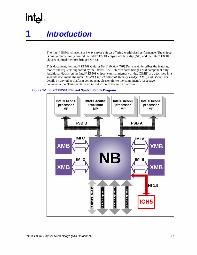
The Intel® E8501 chipset is a 4-way server chipset offering world class performance. The chipset is built architecturally around the Intel® E8501 chipset north bridge (NB) and the Intel® E8501 chipset external memory bridge (XMB).
This document, the Intel® E8501 Chipset North Bridge (NB) Datasheet, describes the features, modes and registers supported by the Intel® E8501 chipset north bridge (NB) component only. Additional details on the Intel® E8501 chipset external memory bridge (XMB) are described in a separate document, the Intel® E8501 Chipset eXternal Memory Bridge (XMB) Datasheet. For details on any other platform component, please refer to the component’s respective documentation. This chapter is an introduction to the entire platform.
Figure 1-1. Intel® E8501 Chipset System Block Diagram
Intel® Xeon®processor
MP
Intel® Xeon®processor
MP
Intel® Xeon®processor
MP
Intel® Xeon®processor
MP
NBIMI A
IMI BIMI D
IMI C
ICH5
FSB B FSB A
XMBXMB
XMB XMB
HI 1.5
18 Intel® E8501 Chipset North Bridge (NB) Datasheet
Introduction
1.1 Intel® E8501 Chipset North Bridge (NB) Feature ListThe NB is the center of the Intel® E8501 Chipset architecture (refer to Figure 1-1). The NB provides the interconnect to:
• 64-bit Intel® Xeon® processor MP or Dual-Core Intel® Xeon® processor 7000 sequence via two 667 MHz or 800 MHz front side buses optimized for server applications
• XMBs via four Independent Memory Interfaces (IMI)
• I/O components via one x4 & three x8 PCI Express* links and Intel® 82801EB I/O Controller Hub 5 (ICH5) via the HI 1.5
1.1.1 Processor Front Side Bus Support• Supports up to 4 64-bit Intel® Xeon® processor MP or Dual-Core Intel® Xeon® processor
7000 sequence
• 667 MHz or 800 MHz operation
• Maintains coherency across both buses
• Double-pumped 40-bit address buses with ADS every other clock which provides a total address bandwidth of 167 million addresses/second
• Quad-pumped, 64-bit data bus providing a bandwidth of 5.3 GB/s per bus at 667 MHz or 6.4 GB/s per bus at 800 MHz
• In-Order-Queue depth of 12
• Maintains coherency across both buses
• Return data by Enhanced Defer to allow out-of-order completion
• ECC protection on data signals and parity protection on address signals
1.1.2 Independent Memory Interface• 4 Independent Memory Interface (IMI) ports, each with up to 5.33 GB/s inbound (read)
bandwidth and 2.67 GB/s outbound (write) bandwidth simultaneously
• 40-bit addressing support provides one terabyte (240 bytes) addressing capability (this is in excess of maximum physical memory supported by the Intel® E8501 chipset platform)
• Memory technology independent
• Hot-plug support on each IMI
1.1.3 I/O InterfacesThe Intel® E8501 chipset relies primarily on PCI Express to provide the interconnect between the NB and the I/O subsystem. The I/O subsystem is based on one x4 PCI Express link, three x8 PCI Express links (each of which can be split into two x4 links), and one HI1.5 link.
Intel® E8501 Chipset North Bridge (NB) Datasheet 19
Introduction
PCI Express*• One x4 and three x8 links. Each x8 link can be configured as two x4 links, making a total of
seven x4 links
• 1 GB/s bandwidth in each direction for x4 links and 2 GB/s for x8 links
• All ports support Hot-Plug
HI 1.5• 8-bit wide, 4x data transfer, 66 MHz base clock
• 266 MB/s bandwidth
• Legacy I/O interconnection to the ICH5
1.1.4 Transaction Processing Capabilities• 64 transactions processed concurrently
• 128-entry Common Data Cache (CDC) for write combining and write buffering
1.1.5 RASUM• ECC on all internal data paths
• Error Detection and Logging Registers on all interfaces
• CRC32 and CRC16 on PCI Express links
• Packet level CRC on IMI’s
• IMI error recovery support via read or write retry
— Transient DRAM read error recovery
— Transient single IMI wire failure recovery
• Memory mirroring support
• Parity protection on Hub Interface 1.5 (address, control & data)
• Hot-Plug support on PCI Express and IMI ports
• SMBus and JTAG interfaces for system management
• Support for Mirroring of memory
• Parity protected Hub Interface (Address, Control & Data)
1.1.6 Package• 1432 pin FC-BGA3 (42.5 x 42.5 mm) with a pin-pitch of 1.09 mm.
20 Intel® E8501 Chipset North Bridge (NB) Datasheet
Introduction
1.2 Intel® E8501 Chipset eXternal Memory Bridge (XMB) Feature ListThe Intel® E8501 chipset external memory bridge (XMB) is an intelligent memory controller that bridges the IMI and DDR interfaces. Each XMB connects to one of the NB’s four IMI interfaces. The Intel® E8501 chipset may operate with 1 to 4 XMBs.
1.2.1 DDR Memory Support• Dual DDR memory channels operating in lockstep with four DIMM slots per channel
• DIMMS must be populated in pairs, and DIMMS within a pair must be identical
• Supports either DDR at 266 MHz or 333 MHz or DDR2 at 400 MHz
• Supports 256-Mb, 512-Mb, and 1-Gb technologies
• Registered ECC DIMMS required
• Integrated I2C* controller for reading DIMM SPD data
1.2.2 IMI Support• High speed, point-to-point, differential, recovered clock interconnect
• 2.67 GB/s outbound (to the XMB) and 5.33 GB/s inbound (from the XMB) simultaneous bandwidth
• Hot-Plug support
1.2.3 RASUM Features• ECC on all internal data paths
• Error detection and logging registers on all interfaces
• Packet level CRC protection on IMI
• IMI error recovery support via read or write retry
— Transient single IMI wire failure recovery
• Intel® x8 Single Device Data Correction (x8 SDDC) technology
• DIMM demand and patrol scrubbing
• DIMM sparing
• Hardware memory initialization
• Performance counters
• SMBus and JTAG interfaces for system management
• Hot-plug capable IMI
Intel® E8501 Chipset North Bridge (NB) Datasheet 21
Introduction
1.2.4 Intel® E8501 Chipset eXternal Memory Bridge (XMB) Package
• 829-pin FC-BGA3 (37.5 x 37.5 mm) with a pin-pitch of 1.27 mm
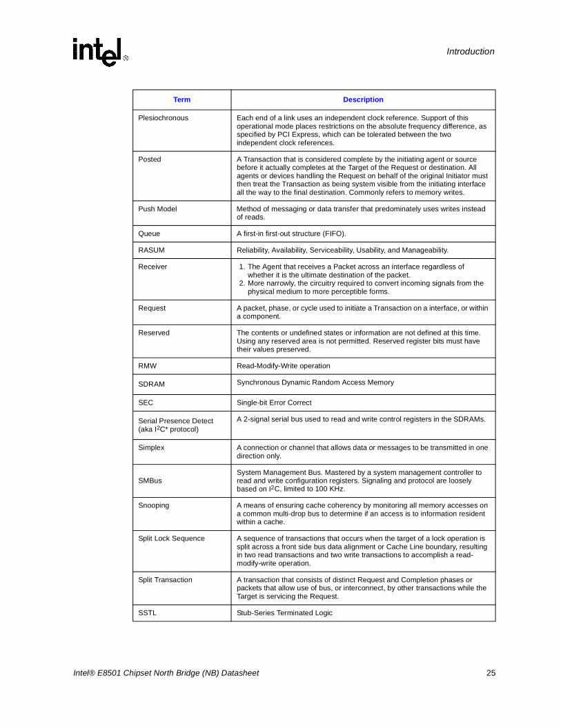
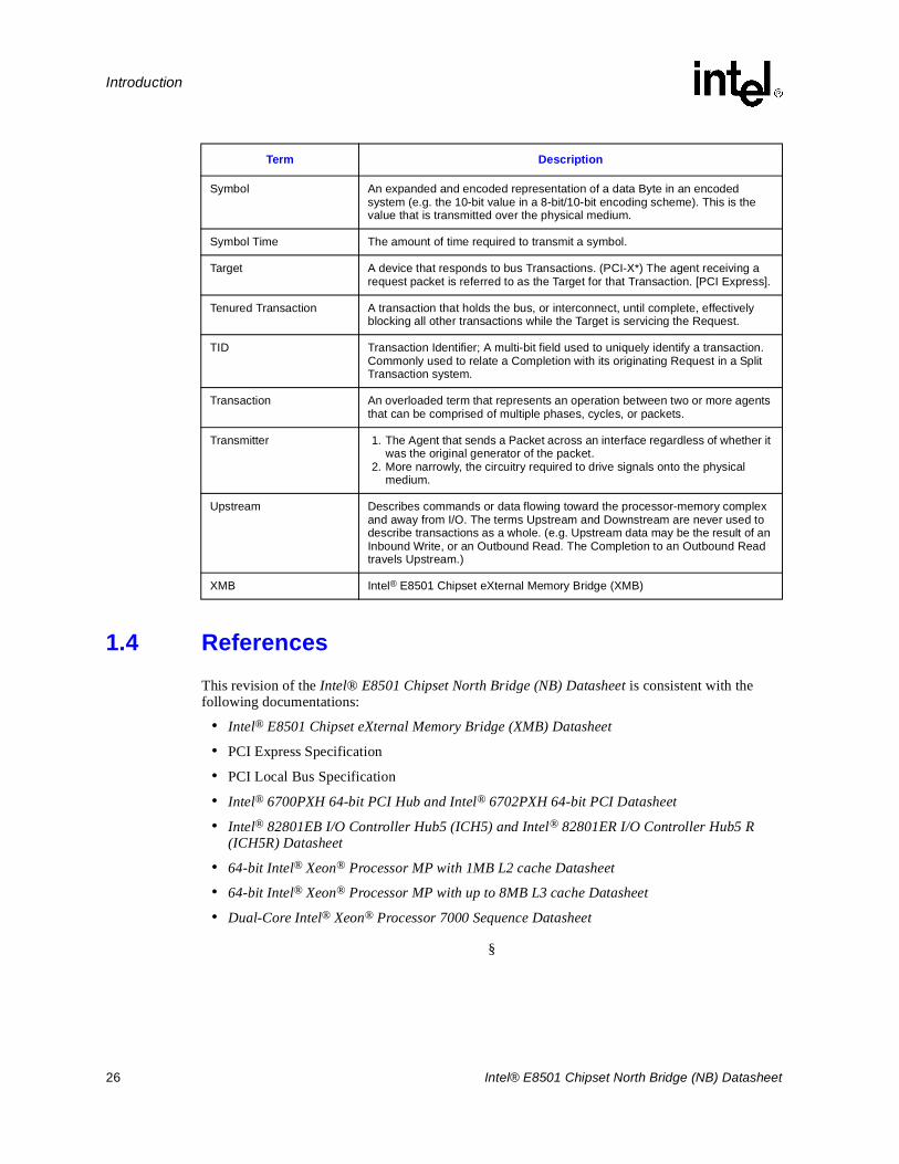
1.3 Terminology
Term Description
Agent A logical device connected to a bus or shared interconnect that can either initiate accesses or be the target of accesses.
Asserted Signal is set to a level that represents logical true.
Asynchronous 1. An event that causes a change in state with no relationship to a clock signal.
2. When applied to transactions or a stream of transactions, a classification for those that do not require service within a fixed time interval.
Atomic operation A series of two or more transactions to a device by the same initiator which are guaranteed to complete without intervening accesses by a different master. Most commonly required for a read-modify-write (RMW) operation.
Bit Interleave,Address Bit Permuting
The way the bits in a cache line are mapped to DIMM rows, banks, and columns (DDR SDRAM) of memory.
Buffer 1. A random access memory structure. 2. The term I/O buffer is also used to describe a low level input receiver and
output driver combination.
Cache Line The unit of memory that is copied to and individually tracked in a cache. Specifically, 64 bytes of data or instructions aligned on a 64-byte physical address boundary.
Cache Line Interleave The way a series of cache lines are mapped to DRAM devices.
Cfg Used as a qualifier for transactions that target PCI configuration address space.
Character The raw data Byte in an encoded system (e.g. the 8b value in a 8b/10b encoding scheme). This is the meaningful quantum of information to be transmitted or that is received across an encoded transmission path.
Coherent Transactions that ensure that the processor's view of memory through the cache is consistent with that obtained through the I/O subsystem.
Command The distinct phases, cycles, or packets that make up a transaction. Requests and Completions are referred to generically as Commands.
Completion A packet, phase, or cycle used to terminate a Transaction on a interface, or within a component. A Completion will always refer to a preceding Request and may or may not include data and/or other information.
Core The internal base logic in the NB.
CRC Cyclic Redundancy Check; A number derived from, and stored or transmitted with, a block of data in order to detect corruption. By recalculating the CRC and comparing it to the value originally transmitted, the receiver can detect some types of transmission errors.
22 Intel® E8501 Chipset North Bridge (NB) Datasheet
Introduction
Critical Word FirstThe Independent Memory Interface specification constrains the XMB to deliver the words of a cache line in a particular order such that the word addressed in the request appears in the first data transfer.
DDR Double Data-Rate memory.
DDR Channel One electrical interface to one or more DIMMs, supporting 8 bytes of data and 1 byte of ECC.
Deasserted Signal is set to a level that represents logical false.
DED Double-bit Error Detect.
Deferred Transaction A front side bus Split Transaction. The requesting agent receives a Deferred Response which allows other transactions to occur on the bus. Later, the response agent completes the original request with a separate Deferred Reply transaction.
Delayed Transaction A transaction where the target retries an initial request, but unknown to the initiator, forwards or services the request on behalf of the initiator and stores the completion or the result of the request. The original initiator subsequently re-issues the request and receives the stored completion.
DFM Design for Manufacturability.
DFT Design for Testability.
DIMM Dual-in-Line Memory Module. A packaging arrangement of memory devices on a socketable substrate.
DIMM Rank That set of SDRAMs on one DDR branch which provides the data packet.
DIMM Slot Receptacle (socket) for a DIMM. Also, the relative physical location of a specific DIMM on a DDR channel.
DIMM Stack A set of DIMMs that share data lines.
Direct Memory Access Method of accessing memory on a system without interrupting the processors on that system.
DMA See Direct Memory Access.
Downstream Describes commands or data flowing away from the processor-memory complex and toward I/O. The terms Upstream and Downstream are never used to describe transactions as a whole. (e.g. Downstream data may be the result of an Outbound Write, or an Inbound Read. The Completion to an Inbound Read travels Downstream).
DRAM Page (Row) The DRAM cells selected by the Row Address.
DW A reference to 32 bits of data on a naturally aligned four-byte boundary (i.e. the least significant two bits of the address are 00b).
ECC Error Correcting Code.
Front Side Bus Processor-to-NB interface. The front side bus in this document refers to operation at 166/333/667 MHz (Bus Clock/Address/Data) or 200/400/800 MHz (Bus Clock/Address/Data) . The front side bus is not compatible with the P6 front side bus.
Full Duplex A connection or channel that allows data or messages to be transmitted in opposite directions simultaneously.
Term Description
Intel® E8501 Chipset North Bridge (NB) Datasheet 23
Introduction
GB/s Gigabytes per second (109 bytes per second).
Gb/s Gigabits per second (109 bits per second).
Half Duplex A connection or channel that allows data or messages to be transmitted in either direction, but not simultaneously.
HI1.5 The Intel proprietary hub interface that connects the NB to the ICH5
Host This term is used synonymously with Processor.
I/O 1. Input/Output. 2. When used as a qualifier to a transaction type, specifies that transaction
targets Intel architecture-specific I/O space. (e.g., I/O read).
Intel® ICH5 The I/O Controller Hub component that contains the legacy I/O functions. It communicates with the NB over a proprietary interconnect called Hub Interface.
Implicit Writeback A snoop initiated data transfer from the bus agent with the modified Cache Line to the memory controller due to an access to that line.
Inbound A transaction where the request destination is the processor-memory complex and is sourced from I/O. The terms Inbound and Outbound refer to transactions as a whole and never to Requests or Completions in isolation. (e.g. An Inbound Read generates Downstream data, whereas an Inbound Write has Upstream data. Even more confusing, the Completion to an Inbound Read travels Downstream.)
Inbound (IB)/Outbound (OB)AKA Upstream/DownStream,Northbound/Southbound,Upbound/Downbound
Up, North, or Inbound is in the direction of the Independent Memory Interface, Down, South, or Outbound is in the direction of other IO (SDRAM, SMBus). orInbound is towards the NB, Outbound is away form it.
Initiator The source of requests. (IBA) An agent sending a request packet on PCI Express is referred to as the Initiator for that Transaction. The Initiator may receive a completion for the Request. [PCI Express]
Isochronous A classification of transactions or a stream of transactions that require service within a fixed time interval.
Layer A level of abstraction commonly used in interface specifications as a tool to group elements related to a basic function of the interface within a layer and to identify key interactions between layers.
Legacy Functional requirements handed down from previous chipsets or PC compatibility requirements from the past.
Line Cache line
Line-AtomicallyAtomic operation on one cache lines. Operations on other lines proceed normally during the line-atomic operation. Other operations to the same cache line are suspended until the line-atomic operation is complete.
Link A full duplex transmission path between any two PCI Express devices.
LSb Least Significant Bit
LSB Least Significant Byte
Term Description
24 Intel® E8501 Chipset North Bridge (NB) Datasheet
Introduction
Master A device or logical entity that is capable of initiating transactions. A Master is any potential Initiator.
Master Abort A response to an illegal request. Reads receive all 1s data. Writes have no effect.
MB/s Megabytes per second (106 bytes per second)
Mem Used as a qualifier for transactions that target memory space. (e.g. A Mem read to I/O)
Memory Issue Committing a request to DDR or, in the case of a read, returning the read header.
Mesochronous Distributed or common referenced clock
Metastability A characteristic of flip flops that describes the state where the output becomes non-deterministic. Most commonly caused by a setup or hold time violation.
MSb Most Significant Bit
MSB Most Significant Byte
MTBF Mean Time Between Failure
NB Intel® E8501 Chipset North Bridge (NB)
Non-Coherent Transactions that may cause the processor's view of memory through the cache to be different with that obtained through the I/O subsystem.
Outbound A transaction where the request destination is I/O and is sourced from the processor-memory complex. The terms Inbound and Outbound refer to transactions as a whole and never to Requests or Completions in isolation. (e.g. An Outbound Read generates Upstream data, whereas an Outbound Write has Downstream data. Even more confusing, the Completion to an Outbound Read travels Upstream.)
PCI-PCI (P-P) Peer-to-Peer Transactions that occur between two devices independent of memory or the processor.
Packet The indivisible unit of data transfer and routing, consisting of a header, data, and CRC.
Page Hit
An access to an open page, or DRAM row. The data can be supplied from the sense amps at low latency. The two halves of the cache line are always placed on the same page, so that only one row command is used. Outside of a cache line the XMB maps address bits to optimize random accesses, at the expense of page hits. Thus page hits outside a cache line are rare.
Page Miss (Empty Page)
An access to a page that is not buffered in sense amps and must be fetched from DRAM array. Address Bit Permuting Address bits are distributed among channel selects, DRAM selects, bank selects to so that a linear address stream accesses these resources in a certain sequence.
Page Replace Aka Page Miss, Row Hit/Page Miss.
An access to a row that has another page open. The page must be transferred back from the sense amps to the array, and the bank must be precharged.
PCI Bus Peripheral Component Interconnect Local Bus. A 32-bit or 64-bit bus with multiplexed address and data lines that is primarily intended for use as an interconnect mechanism within a system between processor/memory and peripheral components or add-in cards.
PCI 2.3 compliant Refers to compliance to the PCI Local Bus Specification, Revision 2.3
Term Description
Intel® E8501 Chipset North Bridge (NB) Datasheet 25
Introduction
Plesiochronous Each end of a link uses an independent clock reference. Support of this operational mode places restrictions on the absolute frequency difference, as specified by PCI Express, which can be tolerated between the two independent clock references.
Posted A Transaction that is considered complete by the initiating agent or source before it actually completes at the Target of the Request or destination. All agents or devices handling the Request on behalf of the original Initiator must then treat the Transaction as being system visible from the initiating interface all the way to the final destination. Commonly refers to memory writes.
Push Model Method of messaging or data transfer that predominately uses writes instead of reads.
Queue A first-in first-out structure (FIFO).
RASUM Reliability, Availability, Serviceability, Usability, and Manageability.
Receiver 1. The Agent that receives a Packet across an interface regardless of whether it is the ultimate destination of the packet.
2. More narrowly, the circuitry required to convert incoming signals from the physical medium to more perceptible forms.
Request A packet, phase, or cycle used to initiate a Transaction on a interface, or within a component.
Reserved The contents or undefined states or information are not defined at this time. Using any reserved area is not permitted. Reserved register bits must have their values preserved.
RMW Read-Modify-Write operation
SDRAM Synchronous Dynamic Random Access Memory
SEC Single-bit Error Correct
Serial Presence Detect (aka I2C* protocol)
A 2-signal serial bus used to read and write control registers in the SDRAMs.
Simplex A connection or channel that allows data or messages to be transmitted in one direction only.
SMBusSystem Management Bus. Mastered by a system management controller to read and write configuration registers. Signaling and protocol are loosely based on I2C, limited to 100 KHz.
Snooping A means of ensuring cache coherency by monitoring all memory accesses on a common multi-drop bus to determine if an access is to information resident within a cache.
Split Lock Sequence A sequence of transactions that occurs when the target of a lock operation is split across a front side bus data alignment or Cache Line boundary, resulting in two read transactions and two write transactions to accomplish a read-modify-write operation.
Split Transaction A transaction that consists of distinct Request and Completion phases or packets that allow use of bus, or interconnect, by other transactions while the Target is servicing the Request.
SSTL Stub-Series Terminated Logic
Term Description
26 Intel® E8501 Chipset North Bridge (NB) Datasheet
Introduction
1.4 ReferencesThis revision of the Intel® E8501 Chipset North Bridge (NB) Datasheet is consistent with the following documentations:
• Intel® E8501 Chipset eXternal Memory Bridge (XMB) Datasheet
• PCI Express Specification
• PCI Local Bus Specification
• Intel® 6700PXH 64-bit PCI Hub and Intel® 6702PXH 64-bit PCI Datasheet
• Intel® 82801EB I/O Controller Hub5 (ICH5) and Intel® 82801ER I/O Controller Hub5 R (ICH5R) Datasheet
• 64-bit Intel® Xeon® Processor MP with 1MB L2 cache Datasheet
• 64-bit Intel® Xeon® Processor MP with up to 8MB L3 cache Datasheet
• Dual-Core Intel® Xeon® Processor 7000 Sequence Datasheet
§
Symbol An expanded and encoded representation of a data Byte in an encoded system (e.g. the 10-bit value in a 8-bit/10-bit encoding scheme). This is the value that is transmitted over the physical medium.
Symbol Time The amount of time required to transmit a symbol.
Target A device that responds to bus Transactions. (PCI-X*) The agent receiving a request packet is referred to as the Target for that Transaction. [PCI Express].
Tenured Transaction A transaction that holds the bus, or interconnect, until complete, effectively blocking all other transactions while the Target is servicing the Request.
TID Transaction Identifier; A multi-bit field used to uniquely identify a transaction. Commonly used to relate a Completion with its originating Request in a Split Transaction system.
Transaction An overloaded term that represents an operation between two or more agents that can be comprised of multiple phases, cycles, or packets.
Transmitter 1. The Agent that sends a Packet across an interface regardless of whether it was the original generator of the packet.
2. More narrowly, the circuitry required to drive signals onto the physical medium.
Upstream Describes commands or data flowing toward the processor-memory complex and away from I/O. The terms Upstream and Downstream are never used to describe transactions as a whole. (e.g. Upstream data may be the result of an Inbound Write, or an Outbound Read. The Completion to an Outbound Read travels Upstream.)
XMB Intel® E8501 Chipset eXternal Memory Bridge (XMB)
Term Description
Intel® E8501 Chipset North Bridge (NB) Datasheet 27
2 Overview
This chapter provides a general overview of the Intel® E8501 chipset North Bridge (NB) and its properties. For functionality details on each interface, please refer to Section 6.
2.1 Logical Pin GroupingFigure 2-1 provides a complete list of the NB signals. The signals are arranged in functional groups according to their associated logical interfaces: FSB{A,B}, IMI{A/B/C/D}, PCI Express{A0/A1/B0/B1/C0/C1/D}, HI1.5, Clock, RAS and Debug. For the complete description of each signal, please refer to Section 3.
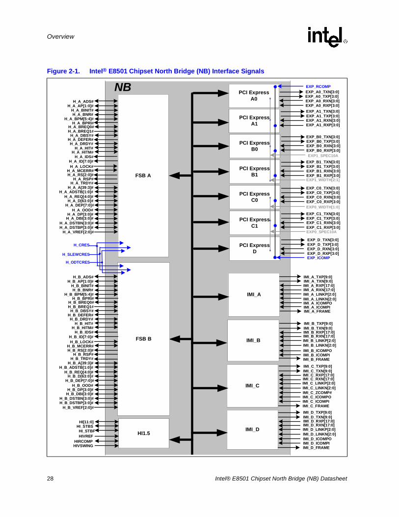
28 Intel® E8501 Chipset North Bridge (NB) Datasheet
Overview
Figure 2-1. Intel® E8501 Chipset North Bridge (NB) Interface Signals
PCI ExpressA0
PCI ExpressA1
PCI ExpressB0
PCI ExpressB1
PCI ExpressC0
PCI ExpressC1
PCI ExpressD
NB
IMI_C
IMI_D
EXP_B0_RXN[3:0]
EXP_B1_RXN[3:0]
EXP_C0_RXN[3:0]
EXP_C1_RXN[3:0]
EXP_D_RXN[3:0]
EXP_B0_TXN[3:0]
EXP_B1_TXN[3:0]
EXP_C0_TXN[3:0]
EXP_C1_TXN[3:0]
EXP_D_TXN[3:0]
EXP_B0_TXP[3:0]
EXP_B1_TXP[3:0]
EXP_C0_TXP[3:0]
EXP_C1_TXP[3:0]
EXP_D_TXP[3:0]
EXP_B0_RXP[3:0]
EXP_B1_RXP[3:0]
EXP_C0_RXP[3:0]
EXP_C1_RXP[3:0]
EXP_D_RXP[3:0]
IMI_A
IMI_B
HI1.5HIVREF
HI[11:0]HI_STBS
HIRCOMPHIVSWING
EXP_A1_RXN[3:0]
EXP_A1_TXN[3:0]EXP_A1_TXP[3:0]
EXP_A1_RXP[3:0]
EXP_A0_RXN[3:0]
EXP_A0_TXN[3:0]EXP_A0_TXP[3:0]
EXP_A0_RXP[3:0]
FSB A
FSB B
H_B_ADS#H_B_AP[1:0]#
H_B_BINIT#H_B_BNR#
H_B_BPM[5:4]#H_B_BPRI#
H_B_BREQ0#H_B_BREQ1#
H_B_DBSY#H_B_DEFER#H_B_DRDY#
H_B_HIT#H_B_HITM#
H_B_IDS#H_B_ID[7:0]#
H_B_MCERR#H_B_LOCK#
H_B_RS[2:0]#H_B_RSP#
H_B_ADSTB[1:0]#
H_B_D[63:0]#
H_B_A[39:3]#H_B_TRDY#
H_B_REQ[4:0]#
H_B_DEP[7:0]#H_B_OOD#
H_B_DP[3:0]#H_B_DBI[3:0]#
H_B_DSTBN[3:0]#H_B_DSTBP[3:0]#
H_B_VREF[2:0]#
H_CRES
H_SLEWCRES
H_ODTCRES
H_A_ADS#H_A_AP[1:0]#
H_A_BINIT#H_A_BNR#
H_A_BPM[5:4]#H_A_BPRI#
H_A_BREQ0#H_A_BREQ1#
H_A_DBSY#H_A_DEFER#H_A_DRDY#
H_A_HIT#H_A_HITM#
H_A_IDS#H_A_ID[7:0]#
H_A_MCERR#H_A_LOCK#
H_A_RS[2:0]#H_A_RSP#
H_A_ADSTB[1:0]#
H_A_D[63:0]#
H_A_A[39:3]#H_A_TRDY#
H_A_REQ[4:0]#
H_A_DEP[7:0]#H_A_OOD#
H_A_DP[3:0]#H_A_DBI[3:0]#
H_A_DSTBN[3:0]#H_A_DSTBP[3:0]#
H_A_VREF[2:0]#
IMI_A_LINKP[2:0]IMI_A_LINKN[2:0]
IMI_A_TXP[9:0]IMI_A_TXN[9:0]IMI_A_RXP[17:0]IMI_A_RXN[17:0]
IMI_A_ICOMPOIMI_A_ICOMPIIMI_A_FRAME
IMI_B_LINKN[2:0]IMI_B_LINKP[2:0]
IMI_B_TXP[9:0]IMI_B_TXN[9:0]IMI_B_RXP[17:0]IMI_B_RXN[17:0]
IMI_B_ICOMPOIMI_B_ICOMPIIMI_B_FRAME
IMI_C_LINKN[2:0]IMI_C_LINKP[2:0]
IMI_C_TXP[9:0]IMI_C_TXN[9:0]IMI_C_RXP[17:0]IMI_C_RXN[17:0]
IMI_C_ZCOMP#IMI_C_ICOMPOIMI_C_ICOMPIIMI_C_FRAME
IMI_D_LINKN[2:0]IMI_D_LINKP[2:0]
IMI_D_TXP[9:0]IMI_D_TXN[9:0]IMI_D_RXP[17:0]IMI_D_RXN[17:0]
IMI_D_ICOMPOIMI_D_ICOMPIIMI_D_FRAME
HI_STBF
EXP_RCOMP
EXP_ICOMP
EXP1_WIDTH[2:1]
EXP0_WIDTH[1:0]
EXP1_SPEC10A
EXP0_SPEC10A
Intel® E8501 Chipset North Bridge (NB) Datasheet 29
Overview
NOTES:1. EXP_HPINT and EXP1_WIDTH1 are muxed names2. PME_OUT and EXP1_WIDTH2 are muxed names
2.2 Quadrant PlacementFor the quadrant and ball placement, refer to Figure 7-1.
2.3 Register DevicesIntel® E8501 chipset configuration registers reside in the NB and the XMB. The registers are grouped into buses, devices, and functions. Figure 2-2 shows the hard-coded bus and function numbers for the NB. All configuration devices in this figure are hard-coded to Bus #0. For detailed information on the register configuration, please refer to Section 4. For hard-coded XMB devices, please refer to the Intel® E8501 Chipset eXternal Memory Bridge (XMB) Datasheet.
Debug
Reset
H_A_RST#H_B_RST#IMI_A_RST#IMI_B_RST#IMI_C_RST#IMI_D_RST#
PWRGOODRSTIN#ICHRST#
Clock&
Analog Power
RAS
IMI_HPINTPME_OUT 2
EXP_HPINT 1
ERROR[2:0]#SMBCLKSMBDATA
ITP_TCKITP_TRST#ITP_TMS
ITP_TDOXDP_D[15:0]#XDP_DSTBP#XDP_DSTBN#XDP_RDY#
ITP_TDI
HI_VSSA
HCLKINNHCLKINP
CLK66
EXP_CLKP
HI_VCCA
EXP_VCCAEXP_VSSA
EXP_CLKN
IMI_{A,B,C,D}_CLKNV3REF[1:0]
XDP_CRESXDP_ODTCRESXDP_SLECRES
IMI_{A,B,C,D}_CLKP
H_VCCAH_VSSA
VCCAVSSA
IMI_{A/B/C/D}_VCCAIMI_{A/B/C/D}_VSSA
EXP_VCCBGEXP_VSSBG
IMI_{A/B/C/D}_VCCBGIMI_{A/B/C/D}_VSSBG
GP_SMBCLKGP_SMBDATA
30 Intel® E8501 Chipset North Bridge (NB) Datasheet
Overview
Figure 2-2. PCI Device Map
NB
VariousBus 0, Dev 0
ICH5
PCI Config Window in I/O Space
PCI BUS 1-9Device 0-n
(Logical PCI Bus #0)
XMBBus 0, Dev 15
IMI_DBus 0, Dev 14
IMI_CBus 0, Dev 12
XMBBus 0, Dev 11
IMI_BBus 0, Dev 10
XMBBus 0, Dev 9
IMI_ABus 0, Dev 8
XMBBus 0, Dev 13
Link A1PCI Express BridgeBus 0, Dev 7
PCI Express BridgeBus 0, Dev 6
Link A0
PCI Express BridgeBus 0, Dev 5
Link B1
PCI Express BridgeBus 0, Dev 4 Link B0
PCI Express BridgeBus 0, Dev 3 Link C1
Link C0PCI Express BridgeBus 0, Dev 2
Link DPCI Express BridgeBus 0, Dev 1
Hub Interface
PSB, Boot & Interrupt F0
Address Mapping F1
RAS F2
Bus 0, Dev 16
HI1.5Bus 0, Dev 0
RESERVEDDev 18, 19 & 20
HI 1.5
HI 1.5
Performance MonitoringBUS 0, Dev 17
Test / DebugBUS 0, Dev 19
Processor Processor Processor Processor
Intel® E8501 Chipset North Bridge (NB) Datasheet 31
Overview
2.4 Intel® E8501 Chipset North Bridge (NB) ClockingThe CK409 is the only clock generator required in a Intel® E8501 chipset platform. Paired with DB800 and DB400 fan-out buffers, this clock solution supplies the reference clocks to all processor and chipset agents. The NB derives the front side bus request and data strobes, XDP debugger data strobes, General Purpose I/O (GPIO) I2C clock, and the SMBus clock from its reference clock.
The reference clock supplying the processors and NB is called “HCLKIN”. The processors and NB populate a low-skew, highly phase-coherent “Common Clock” HCLKIN domain.
Another clock supplied the NB and ICH5 is the Hub Interface Clock, or “CLK66”. The NB and ICH5 populate a low-skew, highly phase-coherent “Common Clock” CLK66 domain. CLK66 can be asynchronous to any other clock on the platform. There is no phase coherence required between HCLKIN and CLK66.
The CK409 also supplies the NB with the PCI Express Clock, or “EXP_CLK”. The PCI Express connections between the NB and PCI Express may be driven from different DB800/DB400 buffers due to their tight part-per-million (ppm) frequency tolerance. Clock skew control between these agents is not required.
2.5 Interrupt DeliveryThe Intel® E8501 chipset supports both the xAPIC and traditional 8259 methods of interrupt delivery. I/O interrupts, and Inter-Processor Interrupts (IPIs) appear as write or interrupt transactions in the system and are delivered to the target processor via the front side bus. This chipset does not support the three-wire sideband bus (the APIC bus). xAPIC interrupts that are generated from I/O devices will need to go through an I/O(x)APIC device unless the device
Figure 2-3. Intel® E8501 Chipset North Bridge (NB) Reference Clocks
CK409
DB800
HCLKINP
HCLKINN
HCLKINP
HCLKINN
CLK66
NBSRC
SRC#
DB800
EXP_CLKP
EXP_CLKN
Other SystemComponents
Other SystemComponents
ICH5
CLK66
32 Intel® E8501 Chipset North Bridge (NB) Datasheet
Overview
supports Message Signalled Interrupts (MSI). In this document, I/O(x)APIC is an interrupt controller. This functionality will be embedded into the Intel 6700PXH 64-bit PCI Hub and ICH5 components of the chipset.
The legacy 8259 functionality is embedded in the ICH5 component. The Intel® E8501 chipset will support inband 8259 interrupt messages from PCI Express devices for boot. The chipset also supports the processor-generated “interrupt acknowledge” (for legacy 8259 interrupts), and “end-of-interrupt” transactions (xAPIC).
2.5.1 xAPIC Interrupt Message DeliveryThe xAPIC interrupt architectures deliver interrupts to the target processor core via interrupt messages presented on the front side bus. Interrupts can originate from I/O(x)APIC devices or processors in the system. Interrupts generated by I/O(x)APIC are in the form of writes with a specific address encoding. Interrupts generated by the processor appear on the front side bus as transactions with a similar address encoding, and a specific encoding on the REQa/REQb signals (REQa=01001, REQb=11100).
The xAPIC architecture provides for lowest priority delivery through interrupt redirection by the chipset. If the redirectable “hint bit” is set in the xAPIC message, the chipset may redirect the interrupt to another processor. Note that redirection of interrupts can be to any processor on either Front Side Bus ID and can be applied to both I/O interrupts and IPIs. The redirection can be performed in logical (flat or clustered) and physical destination modes (these modes are explained in section 6.8.2.2). Figure 2-4 shows the address definition in an IA-32 system (xAPIC). For more information on xAPIC refer to Section 6.8.1, “xAPIC Interrupt Message Delivery” on page 333.
The data field of an interrupt transaction is included in Table 2-1 for reference.
Figure 2-4. xAPIC Address Encoding
rsvd
dm
rhEDID (not used)DID0xFEE
DID: 8-bit destination ID. Software may assign each ID to any valueEDID: Not used. It is a reserved field in the Processor EHSrh: Redirectional bit (0=directional, 1=redirectible)dm: Destination mode (0-physical, 1=logical)*: PCI/PCI Express transaction encoding. Copied to Ab5 on System Bus
02*341112192031
Table 2-1. XAPIC Data Encoding
D[63:16] D[15] D[14] D[13:11] D[10:8] D[7:0]
X Trigger Mode Delivery Status X delivery Mode Vector
Intel® E8501 Chipset North Bridge (NB) Datasheet 33
Overview
2.6 Intel® E8501 Chipset North Bridge (NB) RAS FeaturesThe NB provides a rich set of RAS (Reliability, Availability and Serviceability) features at all its logical interfaces to assure high data integrity, system availability and manageability of the system.
2.6.1 Data Integrity (Error Detection)The NB provides data integrity throughout the component by employing ECC (Error Correcting Codes), CRC (Cyclic Redundancy Checks) and parity on its logical interfaces (Front Side Bus, IMI, PCI Express and HI1.5) as well as ECC on its own internal data paths and buffers (Refer to Figure 2-5).
2.6.1.1 Front Side Bus Interface
• Parity protection on the address lines.
• ECC protection on the data bus.
2.6.1.2 Independent Memory Interface (IMI)
• CRC on outbound control packets.
• CRC and x8 SDDC on inbound data packets.
• Re-issue capability on detected packets that contain a packet CRC errors (errors bad packet will be discarded).
• Transaction ID contained in each packet.
• Transaction retry on time-out or uncorrectable errors.
• 3 virtual signals for errors: FATAL, Uncorrectable and Correctable.
• Hot-Pluggable
2.6.1.3 PCI Express Interface
• 8B/10B encoding at the physical layer.
• CRC on all packets for further data protection (The illegal codes can be detected since not all 8B/10B encoding is used).
• Additional link level mechanisms:PCI Express TrainingSynchronizes the two end of the interface without software intervention to ensure a robust connection.PCI Express RetryIf packets contain errors, the packet will be discarded and the sending end of the interface gets signaled. The sending hardware will re-transmit the particular packet in question and all following packets. Although this will cause a temporary interruption in the delivery of packets, it does so in order to maintain the link integrity.PCI Express RecoveryWhen enough errors occur, the PCI Express link may enter into a quick training sequence,
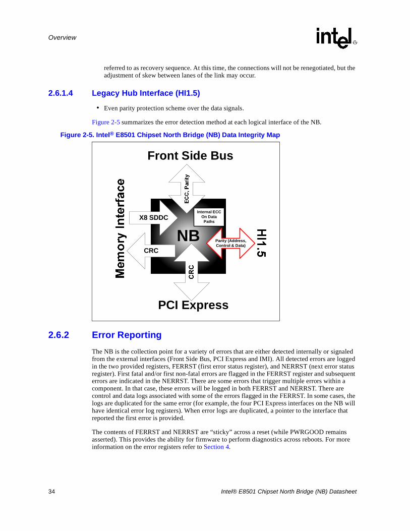
34 Intel® E8501 Chipset North Bridge (NB) Datasheet
Overview
referred to as recovery sequence. At this time, the connections will not be renegotiated, but the adjustment of skew between lanes of the link may occur.
2.6.1.4 Legacy Hub Interface (HI1.5)
• Even parity protection scheme over the data signals.
Figure 2-5 summarizes the error detection method at each logical interface of the NB.
2.6.2 Error ReportingThe NB is the collection point for a variety of errors that are either detected internally or signaled from the external interfaces (Front Side Bus, PCI Express and IMI). All detected errors are logged in the two provided registers, FERRST (first error status register), and NERRST (next error status register). First fatal and/or first non-fatal errors are flagged in the FERRST register and subsequent errors are indicated in the NERRST. There are some errors that trigger multiple errors within a component. In that case, these errors will be logged in both FERRST and NERRST. There are control and data logs associated with some of the errors flagged in the FERRST. In some cases, the logs are duplicated for the same error (for example, the four PCI Express interfaces on the NB will have identical error log registers). When error logs are duplicated, a pointer to the interface that reported the first error is provided.
The contents of FERRST and NERRST are “sticky” across a reset (while PWRGOOD remains asserted). This provides the ability for firmware to perform diagnostics across reboots. For more information on the error registers refer to Section 4.
Figure 2-5. Intel® E8501 Chipset North Bridge (NB) Data Integrity Map
NB
Front Side Bus
PCI Express
Parity (Address,Control & Data)
X8 SDDCInternal ECC
On DataPaths
CRC
Intel® E8501 Chipset North Bridge (NB) Datasheet 35
Overview
2.6.3 Memory MirroringThe Memory Mirroring enables redundancy by always keeping an exact duplicate of memory accessible. The Memory Mirroring logic is located in the NB and is a user selectable feature. At configuration time, the user can enable mirroring and select which IMI Ports are mirrored. The IMI port mirroring options are as follows:
• IMI Port A and B are mirrored, IMI Port C and D are mirrored.
• IMI Port A and C are mirrored, IMI Port B and D are mirrored.
Mirroring control registers include REDUN (Section 4.19.9), IMIST (Section 4.13.9) and IMIHPC (Section 4.13.10) registers.
For a detailed description of mirroring, including the Hot-Plug and re-silvering in mirroring mode, refer to Section 6.3.
2.6.4 Memory RAIDThe Memory RAID enables the data to be reconstructed upon failure behind the IMI ports. The Memory RAID logic is located in the NB and is a user selectable feature. At configuration time, the user can enable memory RAID.
Note: The NB cannot be configured to be in Memory Mirroring Mode and RAID mode at the same time, as these features are mutually exclusive. Also, in order to enable the Memory RAID, the platform must be configured with four XMBs with matching memory configurations.
Raid control registers include REDUN (Section 4.19.9), IMIST (Section 4.13.9) and IMIHPC registers (Section 4.13.10).
For a detailed description of RAID, including the Hot-Plug and re-silvering in RAID mode, refer to Section 6.3.
2.6.5 Hot-PlugPCI Express – All the PCI Express ports are Hot-Pluggable. For more information refer to Section 6.4.8, “Hot-Plug” on page 314.
IMI – The NB provides the ability to add or remove each XMB and the memory behind it to or from any IMI port interface from a running OS instance. The details of the support will be provided in the future revision of this document. For more information refer to Section 6.3.8, “IMI Hot-Plug” on page 287.
Note: In addition to the above Hot-Plug support on the NB, the Intel® E8501 chipset offers Hot-Plug support at the Intel® 6700PXH 64-bit PCI Hub (PCI-X*) interface as well. For detail on application and implication of this component, please refer to Intel® 6700PXH 64-bit PCI Hub and Intel® 6702PXH 64-bit PCI Hub Datasheet.
§

36 Intel® E8501 Chipset North Bridge (NB) Datasheet
Overview
Intel® E8501 Chipset North Bridge (NB) Datasheet 37
3 Signal Description
This section provides a detailed description of the Intel® E8501 chipset north bridge (NB) signals. The signals are arranged in functional groups according to their associated interface. The summary of all signals are also captured on Figure 2-1 “Intel® E8501 Chipset North Bridge (NB) Interface Signals” on page 28.
3.1 ConventionsThe terms assertion and de-assertion are used extensively when describing signals, to avoid confusion when working with a mix of active-high and active-low signals. The term assert, or assertion, indicates that the signal is active, independent of whether the active level is represented by a high or low voltage. The term de-assert, or de-assertion, indicates that the signal is inactive.
Signal names may or may not have a “#” appended to them. The “#” symbol at the end of a signal name indicates that the active, or asserted state occurs when the signal is at a low voltage level. When “#” is not present after the signal name the signal is asserted when at the high voltage level.
Differential signal pairs adopt a “{P/N}” suffix to indicate the “positive” (P) or “negative” (N) signal in the pair. If a “#” is appended, it will be appended to both.
When discussing data values used inside the component, the logical value is used (i.e. a data value described as “1101b” would appear as “1101b” on an active-high bus, and as “0010b” on an active-low bus). When discussing the assertion of a value on the actual signal, the physical value is used (i.e. asserting an active-low signal produces a “0” value on the signal).
Some signals or groups of signals have multiple versions. These signal groups may represent distinct but similar ports or interfaces, or may represent identical copies of the signal used to reduce loading effects. Table 3-1 shows the conventions used in this document.
Curly-bracketed, non-trailing numerical indices (e.g. “{X/Y}”) represent replications of major buses. Square-bracketed numerical indices (e.g. “[n:m]” represent functionally similar but logically distinct bus signals; each signal provides an independent control, and may or may not be asserted at the same time as the other signals in the grouping). In contrast, trailing curly-bracketed numerical indices, e.g., “{x/y}” typically represent identical duplicates of a signal that are provided for electrical reasons.
Table 3-1. Signal Naming Conventions
Convention Expands to
RR{A/B/C}XX Expands to: RRAXX, RRBXX, and RRCXX. This denotes similar signals on replicated buses.
RR[2:0] Expands to: RR[2], RR[1], and RR[0]. This denotes a bus.
RR{A/B/C} Expands to: RRA, RRB, and RRC. This denotes electrical duplicates.
RR# or RR[2:0]# Denotes an active low signal or bus.
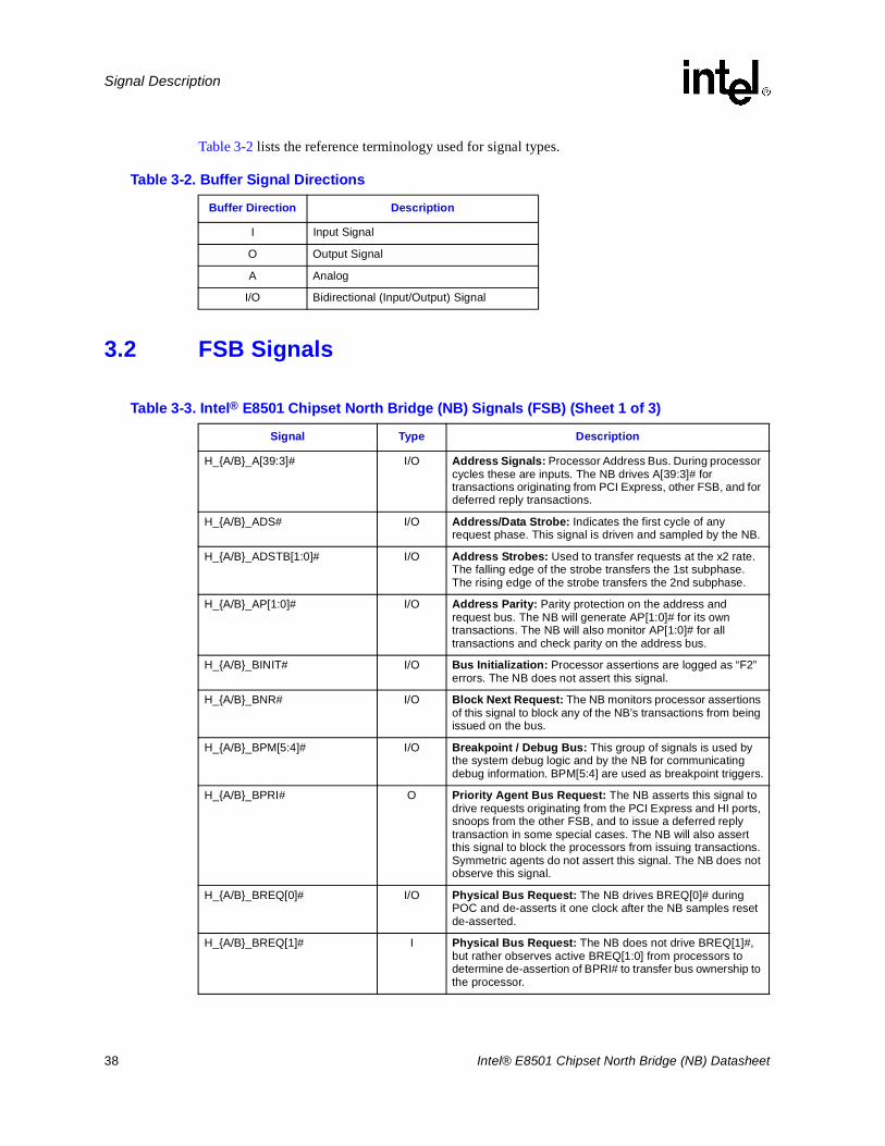
38 Intel® E8501 Chipset North Bridge (NB) Datasheet
Signal Description
Table 3-2 lists the reference terminology used for signal types.
3.2 FSB Signals
Table 3-2. Buffer Signal Directions
Buffer Direction Description
I Input Signal
O Output Signal
A Analog
I/O Bidirectional (Input/Output) Signal
Table 3-3. Intel® E8501 Chipset North Bridge (NB) Signals (FSB) (Sheet 1 of 3)
Signal Type Description
H_{A/B}_A[39:3]# I/O Address Signals: Processor Address Bus. During processor cycles these are inputs. The NB drives A[39:3]# for transactions originating from PCI Express, other FSB, and for deferred reply transactions.
H_{A/B}_ADS# I/O Address/Data Strobe: Indicates the first cycle of any request phase. This signal is driven and sampled by the NB.
H_{A/B}_ADSTB[1:0]# I/O Address Strobes: Used to transfer requests at the x2 rate. The falling edge of the strobe transfers the 1st subphase. The rising edge of the strobe transfers the 2nd subphase.
H_{A/B}_AP[1:0]# I/O Address Parity: Parity protection on the address and request bus. The NB will generate AP[1:0]# for its own transactions. The NB will also monitor AP[1:0]# for all transactions and check parity on the address bus.
H_{A/B}_BINIT# I/O Bus Initialization: Processor assertions are logged as “F2” errors. The NB does not assert this signal.
H_{A/B}_BNR# I/O Block Next Request: The NB monitors processor assertions of this signal to block any of the NB’s transactions from being issued on the bus.
H_{A/B}_BPM[5:4]# I/O Breakpoint / Debug Bus: This group of signals is used by the system debug logic and by the NB for communicating debug information. BPM[5:4] are used as breakpoint triggers.
H_{A/B}_BPRI# O Priority Agent Bus Request: The NB asserts this signal to drive requests originating from the PCI Express and HI ports, snoops from the other FSB, and to issue a deferred reply transaction in some special cases. The NB will also assert this signal to block the processors from issuing transactions. Symmetric agents do not assert this signal. The NB does not observe this signal.
H_{A/B}_BREQ[0]# I/O Physical Bus Request: The NB drives BREQ[0]# during POC and de-asserts it one clock after the NB samples reset de-asserted.
H_{A/B}_BREQ[1]# I Physical Bus Request: The NB does not drive BREQ[1]#, but rather observes active BREQ[1:0] from processors to determine de-assertion of BPRI# to transfer bus ownership to the processor.
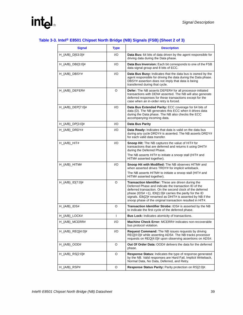
Intel® E8501 Chipset North Bridge (NB) Datasheet 39
Signal Description
H_{A/B}_D[63:0]# I/O Data Bus: 64 bits of data driven by the agent responsible for driving data during the Data phase.
H_{A/B}_DBI[3:0]# I/O Data Bus Inversion: Each bit corresponds to one of the FSB data signal group and 8 bits of ECC.
H_{A/B}_DBSY# I/O Data Bus Busy: Indicates that the data bus is owned by the agent responsible for driving the data during the Data phase. DBSY# assertion does not imply that data is being transferred during that cycle.
H_{A/B}_DEFER# O Defer: The NB asserts DEFER# for all processor-initiated transactions with DEN# asserted. The NB will also generate deferred responses for these transactions except for the case when an in-order retry is forced.
H_{A/B}_DEP[7:0]# I/O Data Bus Extended Parity: ECC coverage for 64 bits of data (D). The NB generates this ECC when it drives data during the Data phase. The NB also checks the ECC accompanying incoming data.
H_{A/B}_DP[3:0]# I/O Data Bus Parity
H_{A/B}_DRDY# I/O Data Ready: Indicates that data is valid on the data bus during any cycle DRDY# is asserted. The NB asserts DRDY# for each valid data transfer.
H_{A/B}_HIT# I/O Snoop Hit: The NB captures the value of HIT# for transactions that are deferred and returns it using DHIT# during the Deferred Phase. The NB asserts HIT# to initiate a snoop stall (HIT# and HITM# asserted together).
H_{A/B}_HITM# I/O Snoop Hit with Modified: The NB observes HITM# and when asserted drives TRDY# for implicit writeback.The NB asserts HITM# to initiate a snoop stall (HIT# and HITM# asserted together).
H_{A/B}_ID[7:0]# O Transaction Identifier: These are driven during the Deferred Phase and indicate the transaction ID of the deferred transaction. On the second clock of the deferred phase (IDS# +1), IDb[1:0]# carries the parity for the ID signals. IDb[2]# renamed as DHIT# is asserted by NB if the snoop phase of the original transaction resulted in HIT#.
H_{A/B}_IDS# O Transaction Identifier Strobe: IDS# is asserted by the NB to indicate the first cycle of the deferred phase.
H_{A/B}_LOCK# I Bus Lock: Indicates atomicity of transactions.
H_{A/B}_MCERR# I/O Machine Check Error: MCERR# indicates non-recoverable bus protocol violation.
H_{A/B}_REQ[4:0]# I/O Request Command: The NB issues requests by driving REQ[4:0]# while asserting ADS#. The NB tracks processor requests on REQ[4:0]# upon observing assertions on ADS#.
H_{A/B}_OOD# O Out Of Order Data: OOD# delivers the data for the deferred phase.
H_{A/B}_RS[2:0]# O Response Status: Indicates the type of response generated by the NB. Valid responses are Hard Fail, Implicit Writeback, Normal Data, No Data, Deferred, and Retry.
H_{A/B}_RSP# O Response Status Parity: Parity protection on RS[2:0]#.
Table 3-3. Intel® E8501 Chipset North Bridge (NB) Signals (FSB) (Sheet 2 of 3)
Signal Type Description
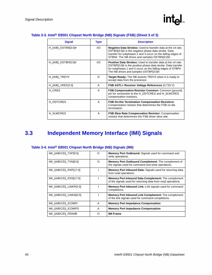
40 Intel® E8501 Chipset North Bridge (NB) Datasheet
Signal Description
3.3 Independent Memory Interface (IMI) Signals
H_{A/B}_DSTBN[3:0]# I/O Negative Data Strobes: Used to transfer data at the x4 rate. DSTBN[3:0]# is the negative phase data strobe. Data transfer for subphases 2 and 4 occur on the falling edges of STBN#. The NB drives and samples DSTBN[3:0]#.
H_{A/B}_DSTBP[3:0]# I/O Positive Data Strobes: Used to transfer data at the x4 rate. DSTBP[3:0]# is the positive phase data strobe. Data transfer for subphases 1 and 3 occur on the falling edges of STBP#. The NB drives and samples DSTBP[3:0]#.
H_{A/B}_TRDY# O Target Ready: The NB asserts TRDY# when it is ready to accept data from the processor.
H_{A/B}_VREF[2:0] A FSB AGTL+ Receiver Voltage References (0.733 V)
H_CRES A FSB Compensation Resistor Common: Common (ground) pin for connection to the H_ODTCRES and H_SLWCRES compensation resistors.
H_ODTCRES A FSB On-Die Termination Compensation Resistors:Compensation resistor that determines the FSB on-die termination.
H_SLWCRES A FSB Slew Rate Compensation Resistor: Compensation resistor that determines the FSB driver slew rate.
Table 3-4. Intel® E8501 Chipset North Bridge (NB) Signals (IMI)IMI_{A/B/C/D}_TXP[9:0] O Memory Port Outbound: Signals used for command and
write operations.
IMI_{A/B/C/D}_TXN[9:0] O Memory Port Outbound Complement: The complement of the signals used for command and write operations.
IMI_{A/B/C/D}_RXP[17:0] I Memory Port Inbound Data: Signals used for returning data from read operations.
IMI_{A/B/C/D}_RXN[17:0] I Memory Port Inbound Data Complement: The complement of the signals used for returning data from read operations.
IMI_{A/B/C/D}_LINKP[2:0] I Memory Port Inbound Link: Link signals used for command completions.
IMI_{A/B/C/D}_LINKN[2:0] I Memory Port Inbound Link Complement: The complement of the link signals used for command completions.
IMI_{A/B/C/D}_ICOMPI A Memory Port Impedance Compensation
IMI_{A/B/C/D}_ICOMPO A Memory Port Impedance Compensation
IMI_{A/B/C/D}_FRAME O IMI Frame
Table 3-3. Intel® E8501 Chipset North Bridge (NB) Signals (FSB) (Sheet 3 of 3)
Signal Type Description
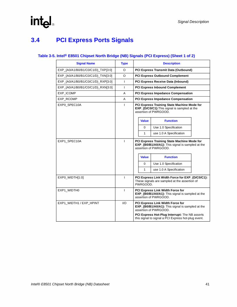
Intel® E8501 Chipset North Bridge (NB) Datasheet 41
Signal Description
3.4 PCI Express Ports Signals
Table 3-5. Intel® E8501 Chipset North Bridge (NB) Signals (PCI Express) (Sheet 1 of 2)
Signal Name Type Description
EXP_{A0/A1/B0/B1/C0/C1/D}_TXP[3:0] O PCI Express Transmit Data (Outbound)
EXP_{A0/A1/B0/B1/C0/C1/D}_TXN[3:0] O PCI Express Outbound Complement
EXP_{A0/A1/B0/B1/C0/C1/D}_RXP[3:0] I PCI Express Receive Data (Inbound)
EXP_{A0/A1/B0/B1/C0/C1/D}_RXN[3:0] I PCI Express Inbound Complement
EXP_ICOMP A PCI Express Impedance Compensation
EXP_RCOMP A PCI Express Impedance Compensation
EXP0_SPEC10A I PCI Express Training State Machine Mode for EXP_{D/C0/C1}:This signal is sampled at the assertion of PWRGOOD.
EXP1_SPEC10A I PCI Express Training State Machine Mode for EXP_{B0/B1/A0/A1}: This signal is sampled at the assertion of PWRGOOD.
EXP0_WIDTH[1:0] I PCI Express Link Width Force for EXP_{D/C0/C1}: These signals are sampled at the assertion of PWRGOOD.
EXP1_WIDTH0 I PCI Express Link Width Force for EXP_{B0/B1/A0/A1}: This signal is sampled at the assertion of PWRGOOD.
EXP1_WIDTH1 / EXP_HPINT I/O PCI Express Link Width Force for EXP_{B0/B1/A0/A1}: This signal is sampled at the assertion of PWRGOOD.PCI Express Hot-Plug Interrupt: The NB asserts this signal to signal a PCI Express hot-plug event.
Value Function
0 Use 1.0 Specification
1 use 1.0 A Specification
Value Function
0 Use 1.0 Specification
1 use 1.0 A Specification
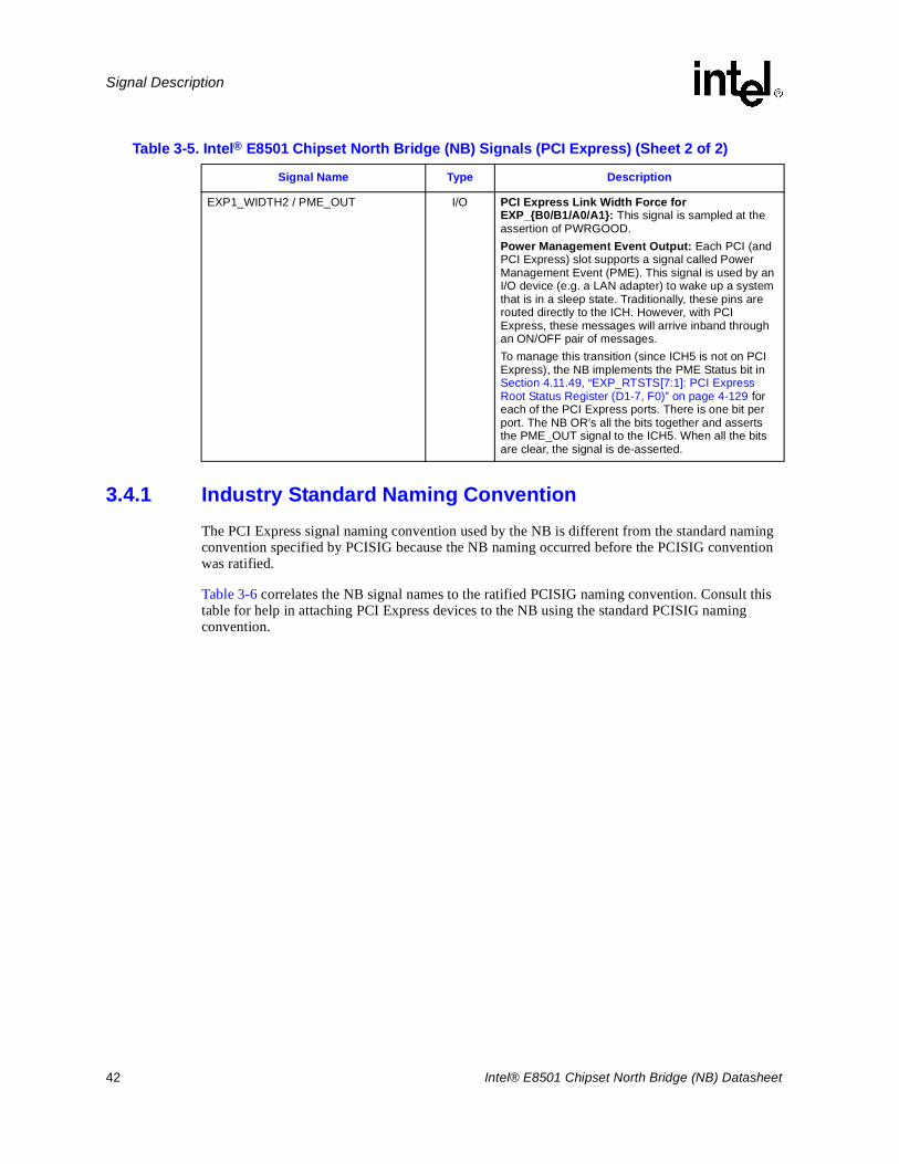
42 Intel® E8501 Chipset North Bridge (NB) Datasheet
Signal Description
3.4.1 Industry Standard Naming Convention The PCI Express signal naming convention used by the NB is different from the standard naming convention specified by PCISIG because the NB naming occurred before the PCISIG convention was ratified.
Table 3-6 correlates the NB signal names to the ratified PCISIG naming convention. Consult this table for help in attaching PCI Express devices to the NB using the standard PCISIG naming convention.
EXP1_WIDTH2 / PME_OUT I/O PCI Express Link Width Force for EXP_{B0/B1/A0/A1}: This signal is sampled at the assertion of PWRGOOD.Power Management Event Output: Each PCI (and PCI Express) slot supports a signal called Power Management Event (PME). This signal is used by an I/O device (e.g. a LAN adapter) to wake up a system that is in a sleep state. Traditionally, these pins are routed directly to the ICH. However, with PCI Express, these messages will arrive inband through an ON/OFF pair of messages.To manage this transition (since ICH5 is not on PCI Express), the NB implements the PME Status bit in Section 4.11.49, “EXP_RTSTS[7:1]: PCI Express Root Status Register (D1-7, F0)” on page 4-129 for each of the PCI Express ports. There is one bit per port. The NB OR’s all the bits together and asserts the PME_OUT signal to the ICH5. When all the bits are clear, the signal is de-asserted.
Table 3-5. Intel® E8501 Chipset North Bridge (NB) Signals (PCI Express) (Sheet 2 of 2)
Signal Name Type Description
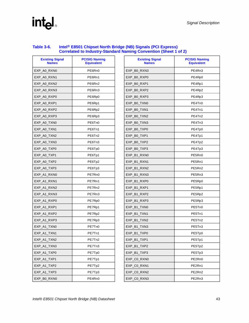
Intel® E8501 Chipset North Bridge (NB) Datasheet 43
Signal Description
Table 3-6. Intel® E8501 Chipset North Bridge (NB) Signals (PCI Express) Correlated to Industry-Standard Naming Convention (Sheet 1 of 2)
Existing Signal Names
PCISIG Naming Equivalent
Existing Signal Names
PCISIG Naming Equivalent
EXP_A0_RXN0 PE6Rn0 EXP_B0_RXN3 PE4Rn3
EXP_A0_RXN1 PE6Rn1 EXP_B0_RXP0 PE4Rp0
EXP_A0_RXN2 PE6Rn2 EXP_B0_RXP1 PE4Rp1
EXP_A0_RXN3 PE6Rn3 EXP_B0_RXP2 PE4Rp2
EXP_A0_RXP0 PE6Rp0 EXP_B0_RXP3 PE4Rp3
EXP_A0_RXP1 PE6Rp1 EXP_B0_TXN0 PE4Tn0
EXP_A0_RXP2 PE6Rp2 EXP_B0_TXN1 PE4Tn1
EXP_A0_RXP3 PE6Rp3 EXP_B0_TXN2 PE4Tn2
EXP_A0_TXN0 PE6Tn0 EXP_B0_TXN3 PE4Tn3
EXP_A0_TXN1 PE6Tn1 EXP_B0_TXP0 PE4Tp0
EXP_A0_TXN2 PE6Tn2 EXP_B0_TXP1 PE4Tp1
EXP_A0_TXN3 PE6Tn3 EXP_B0_TXP2 PE4Tp2
EXP_A0_TXP0 PE6Tp0 EXP_B0_TXP3 PE4Tp3
EXP_A0_TXP1 PE6Tp1 EXP_B1_RXN0 PE5Rn0
EXP_A0_TXP2 PE6Tp2 EXP_B1_RXN1 PE5Rn1
EXP_A0_TXP3 PE6Tp3 EXP_B1_RXN2 PE5Rn2
EXP_A1_RXN0 PE7Rn0 EXP_B1_RXN3 PE5Rn3
EXP_A1_RXN1 PE7Rn1 EXP_B1_RXP0 PE5Rp0
EXP_A1_RXN2 PE7Rn2 EXP_B1_RXP1 PE5Rp1
EXP_A1_RXN3 PE7Rn3 EXP_B1_RXP2 PE5Rp2
EXP_A1_RXP0 PE7Rp0 EXP_B1_RXP3 PE5Rp3
EXP_A1_RXP1 PE7Rp1 EXP_B1_TXN0 PE5Tn0
EXP_A1_RXP2 PE7Rp2 EXP_B1_TXN1 PE5Tn1
EXP_A1_RXP3 PE7Rp3 EXP_B1_TXN2 PE5Tn2
EXP_A1_TXN0 PE7Tn0 EXP_B1_TXN3 PE5Tn3
EXP_A1_TXN1 PE7Tn1 EXP_B1_TXP0 PE5Tp0
EXP_A1_TXN2 PE7Tn2 EXP_B1_TXP1 PE5Tp1
EXP_A1_TXN3 PE7Tn3 EXP_B1_TXP2 PE5Tp2
EXP_A1_TXP0 PE7Tp0 EXP_B1_TXP3 PE5Tp3
EXP_A1_TXP1 PE7Tp1 EXP_C0_RXN0 PE2Rn0
EXP_A1_TXP2 PE7Tp2 EXP_C0_RXN1 PE2Rn1
EXP_A1_TXP3 PE7Tp3 EXP_C0_RXN2 PE2Rn2
EXP_B0_RXN0 PE4Rn0 EXP_C0_RXN3 PE2Rn3
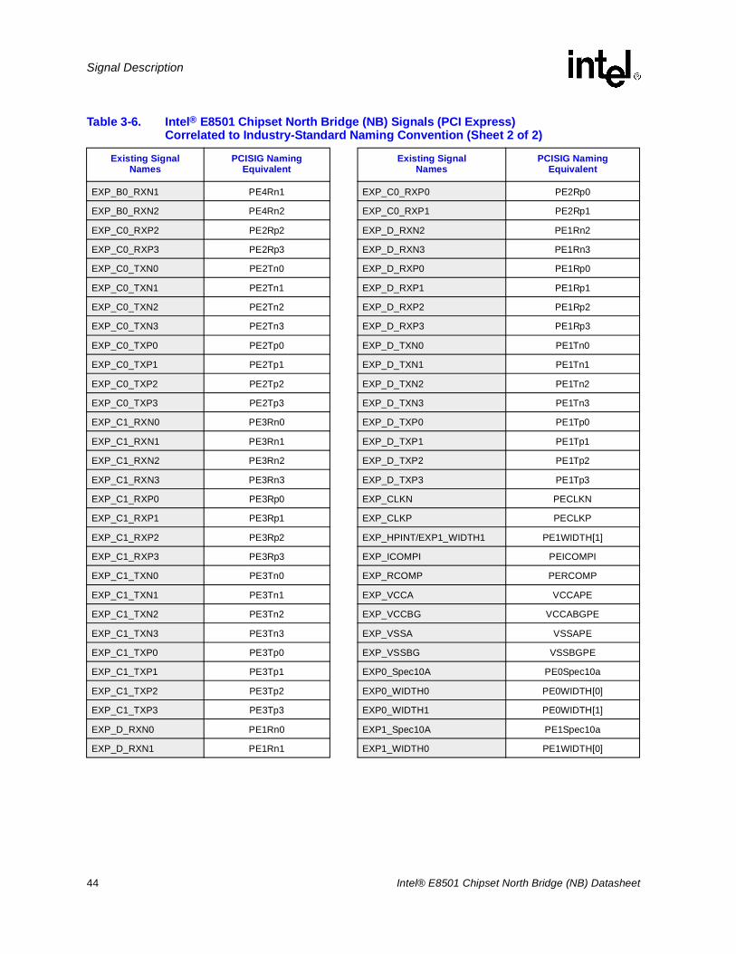
44 Intel® E8501 Chipset North Bridge (NB) Datasheet
Signal Description
EXP_B0_RXN1 PE4Rn1 EXP_C0_RXP0 PE2Rp0
EXP_B0_RXN2 PE4Rn2 EXP_C0_RXP1 PE2Rp1
EXP_C0_RXP2 PE2Rp2 EXP_D_RXN2 PE1Rn2
EXP_C0_RXP3 PE2Rp3 EXP_D_RXN3 PE1Rn3
EXP_C0_TXN0 PE2Tn0 EXP_D_RXP0 PE1Rp0
EXP_C0_TXN1 PE2Tn1 EXP_D_RXP1 PE1Rp1
EXP_C0_TXN2 PE2Tn2 EXP_D_RXP2 PE1Rp2
EXP_C0_TXN3 PE2Tn3 EXP_D_RXP3 PE1Rp3
EXP_C0_TXP0 PE2Tp0 EXP_D_TXN0 PE1Tn0
EXP_C0_TXP1 PE2Tp1 EXP_D_TXN1 PE1Tn1
EXP_C0_TXP2 PE2Tp2 EXP_D_TXN2 PE1Tn2
EXP_C0_TXP3 PE2Tp3 EXP_D_TXN3 PE1Tn3
EXP_C1_RXN0 PE3Rn0 EXP_D_TXP0 PE1Tp0
EXP_C1_RXN1 PE3Rn1 EXP_D_TXP1 PE1Tp1
EXP_C1_RXN2 PE3Rn2 EXP_D_TXP2 PE1Tp2
EXP_C1_RXN3 PE3Rn3 EXP_D_TXP3 PE1Tp3
EXP_C1_RXP0 PE3Rp0 EXP_CLKN PECLKN
EXP_C1_RXP1 PE3Rp1 EXP_CLKP PECLKP
EXP_C1_RXP2 PE3Rp2 EXP_HPINT/EXP1_WIDTH1 PE1WIDTH[1]
EXP_C1_RXP3 PE3Rp3 EXP_ICOMPI PEICOMPI
EXP_C1_TXN0 PE3Tn0 EXP_RCOMP PERCOMP
EXP_C1_TXN1 PE3Tn1 EXP_VCCA VCCAPE
EXP_C1_TXN2 PE3Tn2 EXP_VCCBG VCCABGPE
EXP_C1_TXN3 PE3Tn3 EXP_VSSA VSSAPE
EXP_C1_TXP0 PE3Tp0 EXP_VSSBG VSSBGPE
EXP_C1_TXP1 PE3Tp1 EXP0_Spec10A PE0Spec10a
EXP_C1_TXP2 PE3Tp2 EXP0_WIDTH0 PE0WIDTH[0]
EXP_C1_TXP3 PE3Tp3 EXP0_WIDTH1 PE0WIDTH[1]
EXP_D_RXN0 PE1Rn0 EXP1_Spec10A PE1Spec10a
EXP_D_RXN1 PE1Rn1 EXP1_WIDTH0 PE1WIDTH[0]
Table 3-6. Intel® E8501 Chipset North Bridge (NB) Signals (PCI Express) Correlated to Industry-Standard Naming Convention (Sheet 2 of 2)
Existing Signal Names
PCISIG Naming Equivalent
Existing Signal Names
PCISIG Naming Equivalent
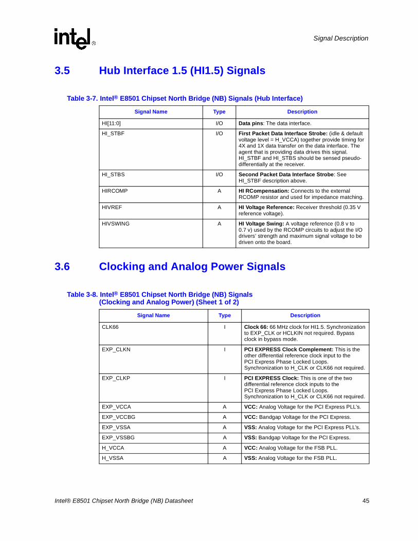
Intel® E8501 Chipset North Bridge (NB) Datasheet 45
Signal Description
3.5 Hub Interface 1.5 (HI1.5) Signals
3.6 Clocking and Analog Power Signals
Table 3-7. Intel® E8501 Chipset North Bridge (NB) Signals (Hub Interface)
Signal Name Type Description
HI[11:0] I/O Data pins: The data interface.
HI_STBF I/O First Packet Data Interface Strobe: (idle & default voltage level = H_VCCA) together provide timing for 4X and 1X data transfer on the data interface. The agent that is providing data drives this signal. HI_STBF and HI_STBS should be sensed pseudo-differentially at the receiver.
HI_STBS I/O Second Packet Data Interface Strobe: See HI_STBF description above.
HIRCOMP A HI RCompensation: Connects to the external RCOMP resistor and used for impedance matching.
HIVREF A HI Voltage Reference: Receiver threshold (0.35 V reference voltage).
HIVSWING A HI Voltage Swing: A voltage reference (0.8 v to 0.7 v) used by the RCOMP circuits to adjust the I/O drivers’ strength and maximum signal voltage to be driven onto the board.
Table 3-8. Intel® E8501 Chipset North Bridge (NB) Signals (Clocking and Analog Power) (Sheet 1 of 2)
Signal Name Type Description
CLK66 I Clock 66: 66 MHz clock for HI1.5. Synchronization to EXP_CLK or HCLKIN not required. Bypass clock in bypass mode.
EXP_CLKN I PCI EXPRESS Clock Complement: This is the other differential reference clock input to the PCI Express Phase Locked Loops. Synchronization to H_CLK or CLK66 not required.
EXP_CLKP I PCI EXPRESS Clock: This is one of the two differential reference clock inputs to the PCI Express Phase Locked Loops. Synchronization to H_CLK or CLK66 not required.
EXP_VCCA A VCC: Analog Voltage for the PCI Express PLL’s.
EXP_VCCBG A VCC: Bandgap Voltage for the PCI Express.
EXP_VSSA A VSS: Analog Voltage for the PCI Express PLL’s.
EXP_VSSBG A VSS: Bandgap Voltage for the PCI Express.
H_VCCA A VCC: Analog Voltage for the FSB PLL.
H_VSSA A VSS: Analog Voltage for the FSB PLL.
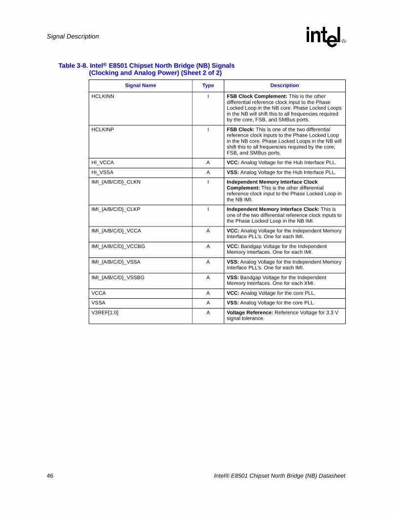
46 Intel® E8501 Chipset North Bridge (NB) Datasheet
Signal Description
HCLKINN I FSB Clock Complement: This is the other differential reference clock input to the Phase Locked Loop in the NB core. Phase Locked Loops in the NB will shift this to all frequencies required by the core, FSB, and SMBus ports.
HCLKINP I FSB Clock: This is one of the two differential reference clock inputs to the Phase Locked Loop in the NB core. Phase Locked Loops in the NB will shift this to all frequencies required by the core, FSB, and SMBus ports.
HI_VCCA A VCC: Analog Voltage for the Hub Interface PLL.
HI_VSSA A VSS: Analog Voltage for the Hub Interface PLL.
IMI_{A/B/C/D}_CLKN I Independent Memory Interface Clock Complement: This is the other differential reference clock input to the Phase Locked Loop in the NB IMI.
IMI_{A/B/C/D}_CLKP I Independent Memory Interface Clock: This is one of the two differential reference clock inputs to the Phase Locked Loop in the NB IMI.
IMI_{A/B/C/D}_VCCA A VCC: Analog Voltage for the Independent Memory Interface PLL’s. One for each IMI.
IMI_{A/B/C/D}_VCCBG A VCC: Bandgap Voltage for the Independent Memory Interfaces. One for each IMI.
IMI_{A/B/C/D}_VSSA A VSS: Analog Voltage for the Independent Memory Interface PLL’s. One for each IMI.
IMI_{A/B/C/D}_VSSBG A VSS: Bandgap Voltage for the Independent Memory Interfaces. One for each XMI.
VCCA A VCC: Analog Voltage for the core PLL.
VSSA A VSS: Analog Voltage for the core PLL.
V3REF[1:0] A Voltage Reference: Reference Voltage for 3.3 V signal tolerance.
Table 3-8. Intel® E8501 Chipset North Bridge (NB) Signals (Clocking and Analog Power) (Sheet 2 of 2)
Signal Name Type Description
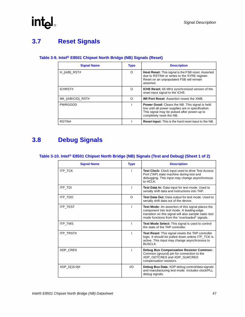
Intel® E8501 Chipset North Bridge (NB) Datasheet 47
Signal Description
3.7 Reset Signals
3.8 Debug Signals
Table 3-9. Intel® E8501 Chipset North Bridge (NB) Signals (Reset)
Signal Name Type Description
H_{A/B}_RST# O Host Reset: This signal is the FSB reset. Asserted due to RSTIN# or writes to the SYRE register. Reset on an unpopulated FSB will remain asserted.
ICHRST# O ICH5 Reset: 66 MHz synchronized version of the reset input signal to the ICH5.
IMI_{A/B/C/D}_RST# O IMI Port Reset: Assertion resets the XMB.
PWRGOOD I Power Good: Clears the NB. This signal is held low until all power supplies are in specification. This signal may be pulsed after power-up to completely reset the NB.
RSTIN# I Reset Input: This is the hard reset input to the NB.
Table 3-10. Intel® E8501 Chipset North Bridge (NB) Signals (Test and Debug) (Sheet 1 of 2)
Signal Name Type Description
ITP_TCK I Test Clock: Clock input used to drive Test Access Port (TAP) state machine during test and debugging. This input may change asynchronous to HCLK.
ITP_TDI I Test Data In: Data input for test mode. Used to serially shift data and instructions into TAP.
ITP_TDO O Test Data Out: Data output for test mode. Used to serially shift data out of the device.
ITP_TEST I Test Mode: An assertion of this signal places the component into test mode. A leading-edge transition on this signal will also sample static test mode functions from the “overloaded” signals.
ITP_TMS I Test Mode Select: This signal is used to control the state of the TAP controller.
ITP_TRST# I Test Reset: This signal resets the TAP controller logic. It should be pulled down unless ITP_TCK is active. This input may change asynchronous to BUSCLK.
XDP_CRES I Debug Bus Compensation Resistor Common:Common (ground) pin for connection to the XDP_ODTCRES and XDP_SLWCRES compensation resistors.
XDP_D[15:0]# I/O Debug Bus Data: XDP debug control/data signals and manufacturing test mode. Includes clock/PLL debug signals.
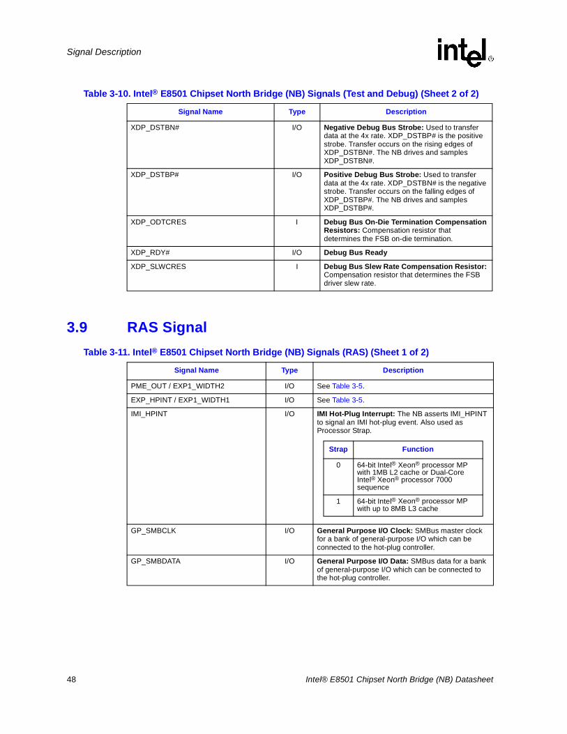
48 Intel® E8501 Chipset North Bridge (NB) Datasheet
Signal Description
3.9 RAS Signal
XDP_DSTBN# I/O Negative Debug Bus Strobe: Used to transfer data at the 4x rate. XDP_DSTBP# is the positive strobe. Transfer occurs on the rising edges of XDP_DSTBN#. The NB drives and samples XDP_DSTBN#.
XDP_DSTBP# I/O Positive Debug Bus Strobe: Used to transfer data at the 4x rate. XDP_DSTBN# is the negative strobe. Transfer occurs on the falling edges of XDP_DSTBP#. The NB drives and samples XDP_DSTBP#.
XDP_ODTCRES I Debug Bus On-Die Termination Compensation Resistors: Compensation resistor that determines the FSB on-die termination.
XDP_RDY# I/O Debug Bus Ready
XDP_SLWCRES I Debug Bus Slew Rate Compensation Resistor:Compensation resistor that determines the FSB driver slew rate.
Table 3-11. Intel® E8501 Chipset North Bridge (NB) Signals (RAS) (Sheet 1 of 2)
Signal Name Type Description
PME_OUT / EXP1_WIDTH2 I/O See Table 3-5.
EXP_HPINT / EXP1_WIDTH1 I/O See Table 3-5.
IMI_HPINT I/O IMI Hot-Plug Interrupt: The NB asserts IMI_HPINT to signal an IMI hot-plug event. Also used as Processor Strap.
GP_SMBCLK I/O General Purpose I/O Clock: SMBus master clock for a bank of general-purpose I/O which can be connected to the hot-plug controller.
GP_SMBDATA I/O General Purpose I/O Data: SMBus data for a bank of general-purpose I/O which can be connected to the hot-plug controller.
Table 3-10. Intel® E8501 Chipset North Bridge (NB) Signals (Test and Debug) (Sheet 2 of 2)
Signal Name Type Description
Strap Function
0 64-bit Intel® Xeon® processor MP with 1MB L2 cache or Dual-Core Intel® Xeon® processor 7000 sequence
1 64-bit Intel® Xeon® processor MP with up to 8MB L3 cache
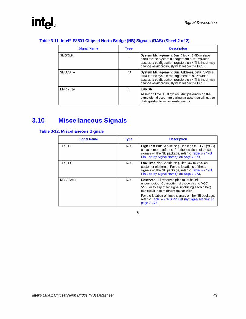
Intel® E8501 Chipset North Bridge (NB) Datasheet 49
Signal Description
3.10 Miscellaneous Signals
§
SMBCLK I System Management Bus Clock: SMBus slave clock for the system management bus. Provides access to configuration registers only. This input may change asynchronously with respect to HCLK.
SMBDATA I/O System Management Bus Address/Data: SMBus data for the system management bus. Provides access to configuration registers only. This input may change asynchronously with respect to HCLK.
ERR[2:0]# O ERROR:Assertion time is 18 cycles. Multiple errors on the same signal occurring during an assertion will not be distinguishable as separate events.
Table 3-12. Miscellaneous Signals
Signal Name Type Description
TESTHI N/A High Test Pin: Should be pulled high to P1V5 (VCC) on customer platforms. For the locations of these signals on the NB package, refer to Table 7-2 “NB Pin List (by Signal Name)” on page 7-373.
TESTLO N/A Low Test Pin: Should be pulled low to VSS on customer platforms. For the locations of these signals on the NB package, refer to Table 7-2 “NB Pin List (by Signal Name)” on page 7-373.
RESERVED N/A Reserved: All reserved pins must be left unconnected. Connection of these pins to VCC, VSS, or to any other signal (including each other) can result in component malfunction.For the location of these signals on the NB package, refer to Table 7-2 “NB Pin List (by Signal Name)” on page 7-373.
Table 3-11. Intel® E8501 Chipset North Bridge (NB) Signals (RAS) (Sheet 2 of 2)
Signal Name Type Description

50 Intel® E8501 Chipset North Bridge (NB) Datasheet
Signal Description
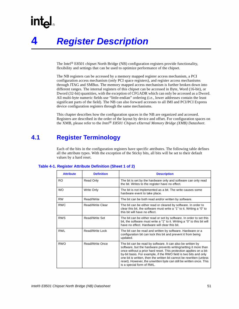
Intel® E8501 Chipset North Bridge (NB) Datasheet 51
4 Register Description
The Intel® E8501 chipset North Bridge (NB) configuration registers provide functionality, flexibility and settings that can be used to optimize performance of the chipset.
The NB registers can be accessed by a memory mapped register access mechanism, a PCI configuration access mechanism (only PCI space registers), and register access mechanisms through JTAG and SMBus. The memory mapped access mechanism is further broken down into different ranges. The internal registers of this chipset can be accessed in Byte, Word (16-bit), or Dword (32-bit) quantities, with the exception of CFGADR which can only be accessed as a Dword. All multi-byte numeric fields use “little-endian” ordering (i.e., lower addresses contain the least significant parts of the field). The NB can also forward accesses to all IMI and PCI/PCI Express device configuration registers through the same mechanisms.
This chapter describes how the configuration spaces in the NB are organized and accessed. Registers are described in the order of the layout by device and offset. For configuration spaces on the XMB, please refer to the Intel® E8501 Chipset eXternal Memory Bridge (XMB) Datasheet.
4.1 Register TerminologyEach of the bits in the configuration registers have specific attributes. The following table defines all the attribute types. With the exception of the Sticky bits, all bits will be set to their default values by a hard reset.
Table 4-1. Register Attribute Definition (Sheet 1 of 2)
Attribute Definition Description
RO Read Only The bit is set by the hardware only and software can only read the bit. Writes to the register have no effect.
WO Write Only The bit is not implemented as a bit. The write causes some hardware event to take place.
RW Read/Write The bit can be both read and/or written by software.
RWC Read/Write Clear The bit can be either read or cleared by software. In order to clear this bit, the software must write a “1” to it. Writing a “0” to this bit will have no effect.
RWS Read/Write Set The bit can be either read or set by software. In order to set this bit, the software must write a “1” to it. Writing a “0” to this bit will have no effect. Hardware will clear this bit.
RWL Read/Write Lock The bit can be read and written by software. Hardware or a configuration bit can lock this bit and prevent it from being updated.
RWO Read/Write Once The bit can be read by software. It can also be written by software, but the hardware prevents writing/setting it more than once without a prior hard reset. This protection applies on a bit-by-bit basis. For example, if the RWO field is two bits and only one bit is written, then the written bit cannot be rewritten (unless reset). However, the unwritten byte can still be written once. This is a special form of RWL.
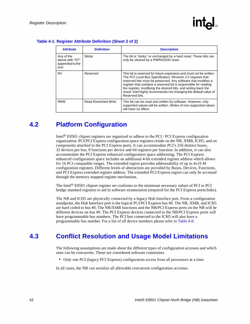
52 Intel® E8501 Chipset North Bridge (NB) Datasheet
Register Description
4.2 Platform Configuration Intel® E8501 chipset registers are organized to adhere to the PCI / PCI Express configuration organization. PCI/PCI Express configuration space registers reside on the NB, XMB, ICH5, and on components attached to the PCI Express ports. It can accommodate PCI’s 256 distinct buses, 32 devices per bus, 8 functions per device and 64 registers per function. In addition, it can also accommodate the PCI Express enhanced configuration space addressing. The PCI Express enhanced configuration space includes an additional 4-bit extended register address which allows for 16 PCI compatible ranges. The extended region provides addressability of up to 4x16 M configuration registers. Different levels of abstraction are provided by Buses, Devices, Functions, and PCI Express extended register address. The extended PCI Express region can only be accessed through the memory mapped register mechanism.
The Intel® E8501 chipset register set conforms to the minimum necessary subset of PCI to PCI bridge standard registers to aid in software enumeration (required for the PCI Express ports/links).
The NB and ICH5 are physically connected by a legacy Hub Interface port. From a configuration standpoint, the Hub Interface port is the logical PCI/PCI Express bus #0. The NB, XMB, and ICH5 are hard coded to bus #0. The NB/XMB functions and the NB/PCI Express ports on the NB will be different devices on bus #0. The PCI Express devices connected to the NB/PCI Express ports will have programmable bus numbers. The PCI bus connected to the ICH5 will also have a programmable bus number. For a list of all device numbers please refer to Table 4-8.
4.3 Conflict Resolution and Usage Model LimitationsThe following assumptions are made about the different types of configuration accesses and which ones can be concurrent. These are considered software constraints.
• Only one PCI (legacy PCI Express) configuration access from all processors at a time.
In all cases, the NB can serialize all allowable concurrent configuration accesses.
Any of the above with “ST” appended to the end
Sticky The bit is “sticky” or unchanged by a hard reset. These bits can only be cleared by a PWRGOOD reset.
RV Reserved This bit is reserved for future expansion and must not be written. The PCI Local Bus Specification, Revision 2.2 requires that reserved bits must be preserved. Any software that modifies a register that contains a reserved bit is responsible for reading the register, modifying the desired bits, and writing back the result. Intel highly recommends not changing the default value of Reserved bits.
RRW Read Restricted Write This bit can be read and written by software. However, only supported values will be written. Writes of non-supported values will have no effect.
Table 4-1. Register Attribute Definition (Sheet 2 of 2)
Attribute Definition Description
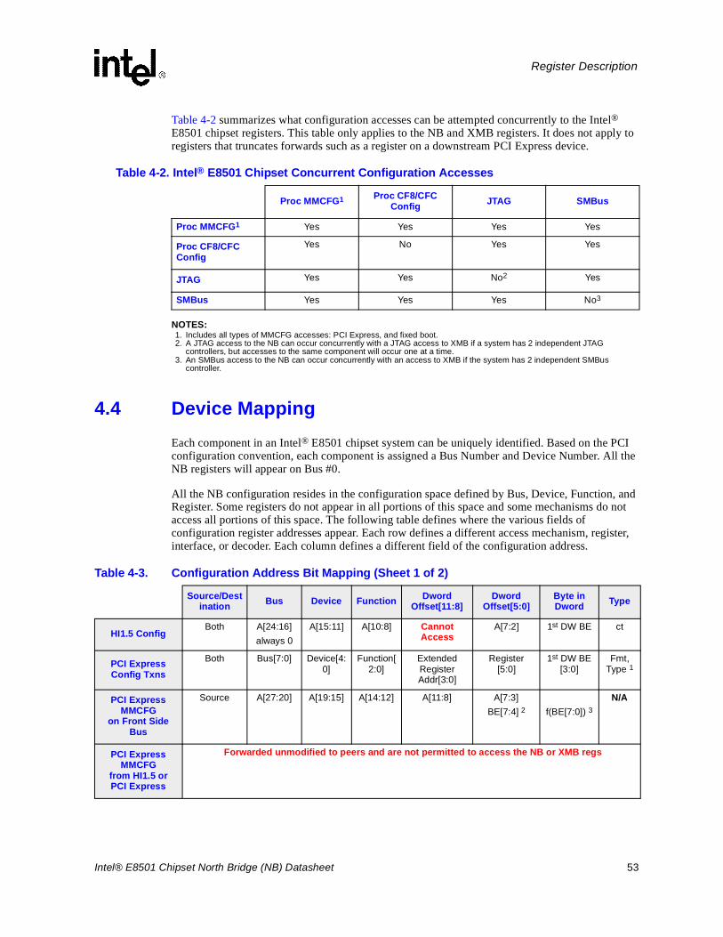
Intel® E8501 Chipset North Bridge (NB) Datasheet 53
Register Description
Table 4-2 summarizes what configuration accesses can be attempted concurrently to the Intel®E8501 chipset registers. This table only applies to the NB and XMB registers. It does not apply to registers that truncates forwards such as a register on a downstream PCI Express device.
NOTES:1. Includes all types of MMCFG accesses: PCI Express, and fixed boot.2. A JTAG access to the NB can occur concurrently with a JTAG access to XMB if a system has 2 independent JTAG
controllers, but accesses to the same component will occur one at a time.3. An SMBus access to the NB can occur concurrently with an access to XMB if the system has 2 independent SMBus
controller.
4.4 Device MappingEach component in an Intel® E8501 chipset system can be uniquely identified. Based on the PCI configuration convention, each component is assigned a Bus Number and Device Number. All the NB registers will appear on Bus #0.
All the NB configuration resides in the configuration space defined by Bus, Device, Function, and Register. Some registers do not appear in all portions of this space and some mechanisms do not access all portions of this space. The following table defines where the various fields of configuration register addresses appear. Each row defines a different access mechanism, register, interface, or decoder. Each column defines a different field of the configuration address.
Table 4-2. Intel® E8501 Chipset Concurrent Configuration Accesses
Proc MMCFG1 Proc CF8/CFC Config JTAG SMBus
Proc MMCFG1 Yes Yes Yes Yes
Proc CF8/CFC Config
Yes No Yes Yes
JTAG Yes Yes No2 Yes
SMBus Yes Yes Yes No3
Table 4-3. Configuration Address Bit Mapping (Sheet 1 of 2)
Source/Destination Bus Device Function Dword
Offset[11:8]Dword
Offset[5:0]Byte in Dword Type
HI1.5 ConfigBoth A[24:16]
always 0A[15:11] A[10:8] Cannot
AccessA[7:2] 1st DW BE ct
PCI Express Config Txns
Both Bus[7:0] Device[4:0]
Function[2:0]
ExtendedRegister Addr[3:0]
Register[5:0]
1st DW BE [3:0]
Fmt,Type 1
PCI Express MMCFG
on Front Side Bus
Source A[27:20] A[19:15] A[14:12] A[11:8] A[7:3]BE[7:4] 2 f(BE[7:0]) 3
N/A
PCI Express MMCFG
from HI1.5 or PCI Express
Forwarded unmodified to peers and are not permitted to access the NB or XMB regs
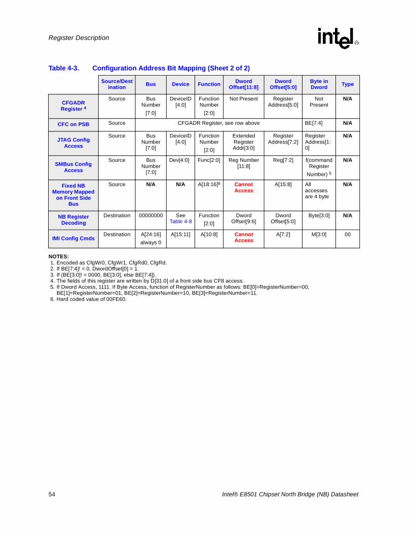
54 Intel® E8501 Chipset North Bridge (NB) Datasheet
Register Description
NOTES:1. Encoded as CfgWr0, CfgWr1, CfgRd0, CfgRd.2. If BE[7:4]! = 0, DwordOffset[0] = 1.3. If (BE[3:0]! = 0000, BE[3:0], else BE[7:4]).4. The fields of this register are written by D[31:0] of a front side bus CF8 access.5. If Dword Access, 1111. If Byte Access, function of RegisterNumber as follows: BE[0]=RegisterNumber=00,
BE[1]=RegisterNumber=01, BE[2]=RegisterNumber=10, BE[3]=RegisterNumber=11.6. Hard coded value of 00FE60.
CFGADR Register 4
Source Bus Number
[7:0]
DeviceID[4:0]
FunctionNumber
[2:0]
Not Present RegisterAddress[5:0]
NotPresent
N/A
CFC on PSB Source CFGADR Register, see row above BE[7:4] N/A
JTAG Config Access
Source Bus Number
[7:0]
DeviceID[4:0]
FunctionNumber
[2:0]
ExtendedRegister Addr[3:0]
RegisterAddress[7:2]
RegisterAddress[1:0]
N/A
SMBus Config Access
Source Bus Number
[7:0]
Dev[4:0] Func[2:0] Reg Number[11:8]
Reg[7:2] f(commandRegister
Number) 5
N/A
Fixed NB Memory Mapped
on Front Side Bus
Source N/A N/A A[18:16]6 Cannot Access
A[15:8] All accesses are 4 byte
N/A
NB Register Decoding
Destination 00000000 See Table 4-8
Function[2:0]
Dword Offset[9:6]
DwordOffset[5:0]
Byte[3:0] N/A
IMI Config CmdsDestination A[24:16]
always 0A[15:11] A[10:8] Cannot
Access A[7:2] M[3:0] 00
Table 4-3. Configuration Address Bit Mapping (Sheet 2 of 2)
Source/Destination Bus Device Function Dword
Offset[11:8]Dword
Offset[5:0]Byte in Dword Type
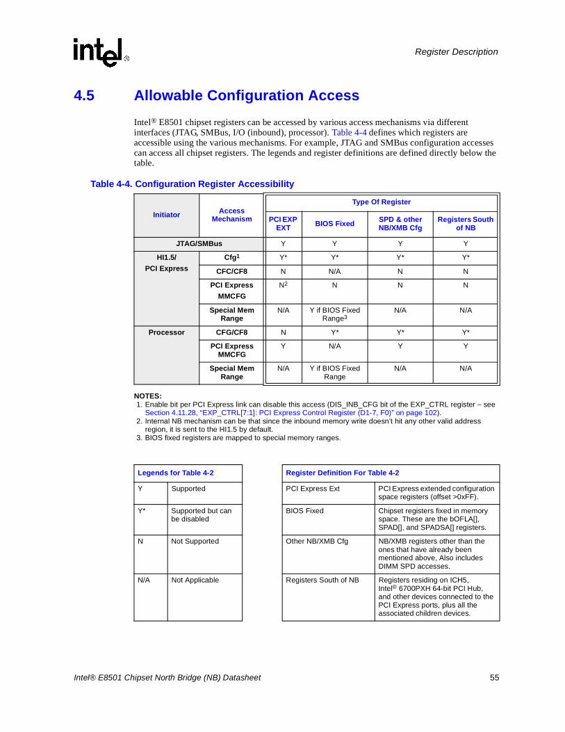
Intel® E8501 Chipset North Bridge (NB) Datasheet 55
Register Description
4.5 Allowable Configuration AccessIntel® E8501 chipset registers can be accessed by various access mechanisms via different interfaces (JTAG, SMBus, I/O (inbound), processor). Table 4-4 defines which registers are accessible using the various mechanisms. For example, JTAG and SMBus configuration accesses can access all chipset registers. The legends and register definitions are defined directly below the table.
NOTES:1. Enable bit per PCI Express link can disable this access (DIS_INB_CFG bit of the EXP_CTRL register – see
Section 4.11.28, “EXP_CTRL[7:1]: PCI Express Control Register (D1-7, F0)” on page 102).2. Internal NB mechanism can be that since the inbound memory write doesn’t hit any other valid address
region, it is sent to the HI1.5 by default.3. BIOS fixed registers are mapped to special memory ranges.
Table 4-4. Configuration Register Accessibility
Initiator AccessMechanism
Type Of Register
PCI EXP EXT BIOS Fixed SPD & other
NB/XMB CfgRegisters South
of NB
JTAG/SMBus Y Y Y Y
HI1.5/PCI Express
Cfg1 Y* Y* Y* Y*
CFC/CF8 N N/A N N
PCI ExpressMMCFG
N2 N N N
Special Mem Range
N/A Y if BIOS Fixed Range3
N/A N/A
Processor CFG/CF8 N Y* Y* Y*
PCI Express MMCFG
Y N/A Y Y
Special Mem Range
N/A Y if BIOS Fixed Range
N/A N/A
Legends for Table 4-2 Register Definition For Table 4-2
Y Supported PCI Express Ext PCI Express extended configuration space registers (offset >0xFF).
Y* Supported but can be disabled
BIOS Fixed Chipset registers fixed in memory space. These are the bOFLA[], SPAD[], and SPADSA[] registers.
N Not Supported Other NB/XMB Cfg NB/XMB registers other than the ones that have already been mentioned above, Also includes DIMM SPD accesses.
N/A Not Applicable Registers South of NB Registers residing on ICH5, Intel® 6700PXH 64-bit PCI Hub, and other devices connected to the PCI Express ports, plus all the associated children devices.
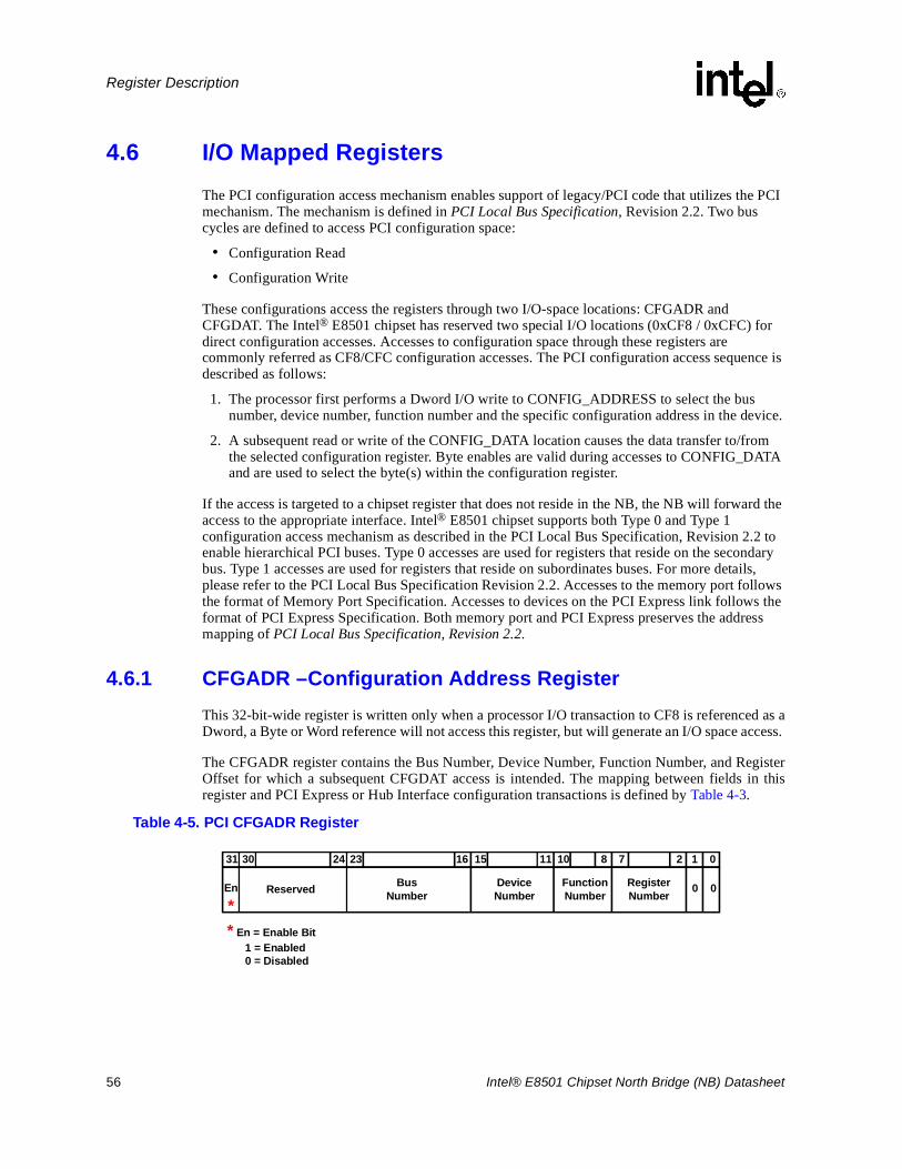
56 Intel® E8501 Chipset North Bridge (NB) Datasheet
Register Description
4.6 I/O Mapped RegistersThe PCI configuration access mechanism enables support of legacy/PCI code that utilizes the PCI mechanism. The mechanism is defined in PCI Local Bus Specification, Revision 2.2. Two bus cycles are defined to access PCI configuration space:
• Configuration Read
• Configuration Write
These configurations access the registers through two I/O-space locations: CFGADR and CFGDAT. The Intel® E8501 chipset has reserved two special I/O locations (0xCF8 / 0xCFC) for direct configuration accesses. Accesses to configuration space through these registers are commonly referred as CF8/CFC configuration accesses. The PCI configuration access sequence is described as follows:
1. The processor first performs a Dword I/O write to CONFIG_ADDRESS to select the bus number, device number, function number and the specific configuration address in the device.
2. A subsequent read or write of the CONFIG_DATA location causes the data transfer to/from the selected configuration register. Byte enables are valid during accesses to CONFIG_DATA and are used to select the byte(s) within the configuration register.
If the access is targeted to a chipset register that does not reside in the NB, the NB will forward the access to the appropriate interface. Intel® E8501 chipset supports both Type 0 and Type 1 configuration access mechanism as described in the PCI Local Bus Specification, Revision 2.2 to enable hierarchical PCI buses. Type 0 accesses are used for registers that reside on the secondary bus. Type 1 accesses are used for registers that reside on subordinates buses. For more details, please refer to the PCI Local Bus Specification Revision 2.2. Accesses to the memory port follows the format of Memory Port Specification. Accesses to devices on the PCI Express link follows the format of PCI Express Specification. Both memory port and PCI Express preserves the address mapping of PCI Local Bus Specification, Revision 2.2.
4.6.1 CFGADR –Configuration Address RegisterThis 32-bit-wide register is written only when a processor I/O transaction to CF8 is referenced as aDword, a Byte or Word reference will not access this register, but will generate an I/O space access.
The CFGADR register contains the Bus Number, Device Number, Function Number, and RegisterOffset for which a subsequent CFGDAT access is intended. The mapping between fields in thisregister and PCI Express or Hub Interface configuration transactions is defined by Table 4-3.
Table 4-5. PCI CFGADR Register
01278101116 1523243031
RegisterNumber
FunctionNumber
DeviceNumber
BusNumberReservedEn
*0 0
* En = Enable Bit 1 = Enabled 0 = Disabled
Intel® E8501 Chipset North Bridge (NB) Datasheet 57
Register Description
4.6.2 CFGDAT –Configuration Data RegisterCFGDAT provides data for the 4 bytes of configuration space defined by CFGADR. This register is only accessed if there is an access to I/O address CFCh on the front side bus and CFGADR.CFGE is set. The byte enables with the IO access define how many configuration bytes are accessed.
4.7 Intel® E8501 Chipset North Bridge (NB) Fixed Mapped RegistersThese registers are mapped into the fixed chipset-specific range located from FE60_0000-FE6F_FFFF. These appear at fixed addresses to support the boot process. These registers also appear in the regular PCI Express configuration space. Table 4-6 defines the memory address of the registers in this region.
I/O Address:CF8h
Bit Attr Default Description
31 RW 0h CFGE: Configuration EnableUnless this bit is set, accesses to the CFGDAT register will not produce a configuration access, but will be treated as other I/O accesses. This bit is strictly an enable for the CFC/CF8 access mechanism and is not forwarded to HI or PCI Express.
30:24 RV 00h Reserved
23:16 RW 00h Bus NumberIf 0, the NB examines device to determine where to route. If non-zero, route as per PBUSN and SBUSN registers.
15:11 RW 0h Device Number
10:8 RW 0h Function NumberThis field is used to select the function of a locally addressed register.
7:2 RW 00h Register OffsetIf this register specifies an access to the NB registers, this field specifies a group of four bytes to be addressed. The bytes accessed are defined by the Byte enables of the CFGDAT register access.
1:0 RW* 0h Writes to these bits will have no effect, reads return 0.
I/O Address:CFCh
Bit Attr Default Description
31:0 RW 0000h Configuration Data WindowThe data written or read to the configuration register (if any) specified by CFGADR.
58 Intel® E8501 Chipset North Bridge (NB) Datasheet
Register Description
4.8 PCI Express Device Configuration RegistersThe PCI Express register structure is exposed to the operating system and requires a separate device per port. Ports A-D will be assigned devices 1 through 7 (refer to Figure 2-2 on page 2-30.)The PCI Express ports determine at reset the width of the devices to which they are connected. If ports are combined to form x8 ports, configuration accesses to the most significant device numbers will still be completed successfully, but only the least significant device number will control and hold status for the wider port.
Table 4-6. Mapping of Fixed Memory Mapped Registers
Register Memory Address
BOFL0 FE60_C000
BOFL1 FE60_C400
BOFL2 FE60_C800
BOFL3 FE60_CC00
SPAD0 FE60_D000
SPAD1 FE60_D400
SPAD2 FE60_D800
SPAD3 FE60_DC00
SPADS0 FE60_E000
SPADS1 FE60_E400
SPADS2 FE60_E800
SPADS3 FE60_EC00
Table 4-7. When will a PCI Express Device be Accessible?
PCI Express Port Device x8 Registers may be accessed if...
A1 7 PossibleCombination
Port A1 is connected to a x4 device.
A0 6 Port A0 is connected to a x4 or x8 device.
B1 5 PossibleCombination
Port B1 is connected to a x4 device.
B0 4 Port B0 is connected to a x4 or x8.
C1 3 PossibleCombination
Port C1 is connected to a x4 device.
C0 2 Port C0 is connected to a x4 or x8 device.
D1 Cannot be a x8
A 4x device is connected to Port D. This port cannot be combined with any other PORT to form an x8.
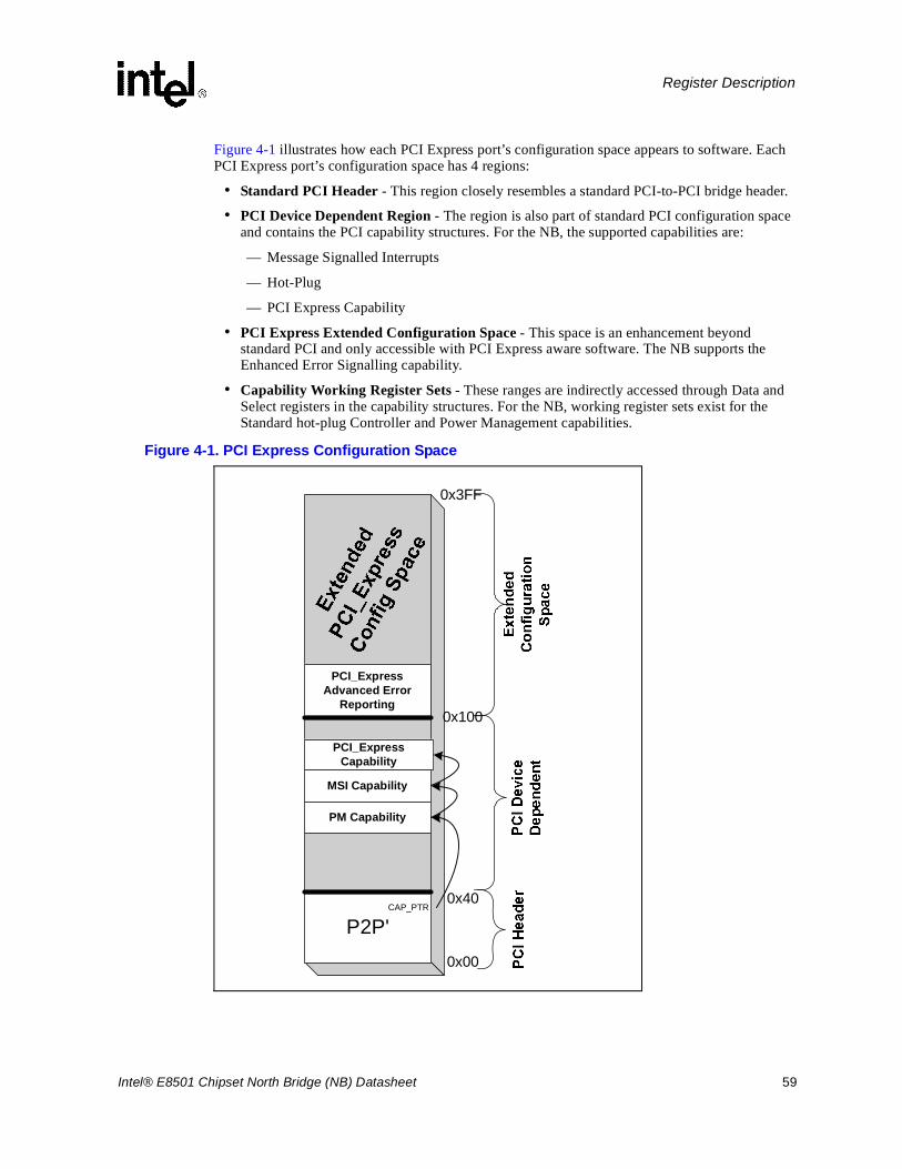
Intel® E8501 Chipset North Bridge (NB) Datasheet 59
Register Description
Figure 4-1 illustrates how each PCI Express port’s configuration space appears to software. Each PCI Express port’s configuration space has 4 regions:
• Standard PCI Header - This region closely resembles a standard PCI-to-PCI bridge header.
• PCI Device Dependent Region - The region is also part of standard PCI configuration space and contains the PCI capability structures. For the NB, the supported capabilities are:
— Message Signalled Interrupts
— Hot-Plug
— PCI Express Capability
• PCI Express Extended Configuration Space - This space is an enhancement beyond standard PCI and only accessible with PCI Express aware software. The NB supports the Enhanced Error Signalling capability.
• Capability Working Register Sets - These ranges are indirectly accessed through Data and Select registers in the capability structures. For the NB, working register sets exist for the Standard hot-plug Controller and Power Management capabilities.
Figure 4-1. PCI Express Configuration Space
0x00
0x40
0x100
0x3FF
PCI_ExpressAdvanced Error
Reporting
PM Capability
MSI Capability
P2P'CAP_PTR
PCI_ExpressCapability
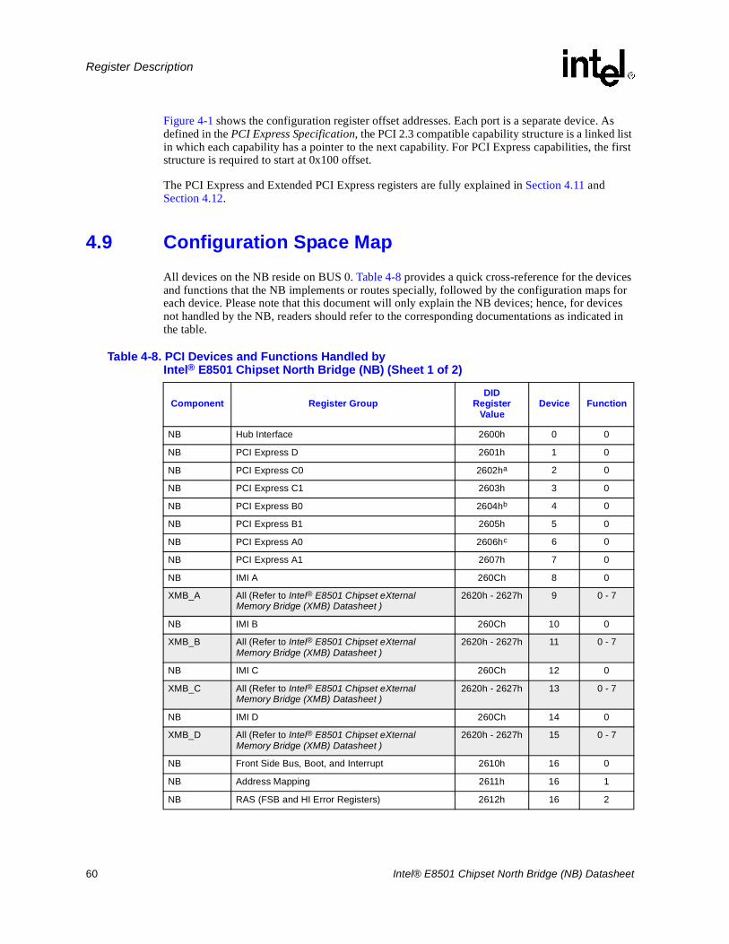
60 Intel® E8501 Chipset North Bridge (NB) Datasheet
Register Description
Figure 4-1 shows the configuration register offset addresses. Each port is a separate device. As defined in the PCI Express Specification, the PCI 2.3 compatible capability structure is a linked list in which each capability has a pointer to the next capability. For PCI Express capabilities, the first structure is required to start at 0x100 offset.
The PCI Express and Extended PCI Express registers are fully explained in Section 4.11 and Section 4.12.
4.9 Configuration Space MapAll devices on the NB reside on BUS 0. Table 4-8 provides a quick cross-reference for the devices and functions that the NB implements or routes specially, followed by the configuration maps for each device. Please note that this document will only explain the NB devices; hence, for devices not handled by the NB, readers should refer to the corresponding documentations as indicated in the table.
Table 4-8. PCI Devices and Functions Handled by Intel® E8501 Chipset North Bridge (NB) (Sheet 1 of 2)
Component Register GroupDID
Register Value
Device Function
NB Hub Interface 2600h 0 0
NB PCI Express D 2601h 1 0
NB PCI Express C0 2602ha 2 0
NB PCI Express C1 2603h 3 0
NB PCI Express B0 2604hb 4 0
NB PCI Express B1 2605h 5 0
NB PCI Express A0 2606hc 6 0
NB PCI Express A1 2607h 7 0
NB IMI A 260Ch 8 0
XMB_A All (Refer to Intel® E8501 Chipset eXternal Memory Bridge (XMB) Datasheet )
2620h - 2627h 9 0 - 7
NB IMI B 260Ch 10 0
XMB_B All (Refer to Intel® E8501 Chipset eXternal Memory Bridge (XMB) Datasheet )
2620h - 2627h 11 0 - 7
NB IMI C 260Ch 12 0
XMB_C All (Refer to Intel® E8501 Chipset eXternal Memory Bridge (XMB) Datasheet )
2620h - 2627h 13 0 - 7
NB IMI D 260Ch 14 0
XMB_D All (Refer to Intel® E8501 Chipset eXternal Memory Bridge (XMB) Datasheet )
2620h - 2627h 15 0 - 7
NB Front Side Bus, Boot, and Interrupt 2610h 16 0
NB Address Mapping 2611h 16 1
NB RAS (FSB and HI Error Registers) 2612h 16 2
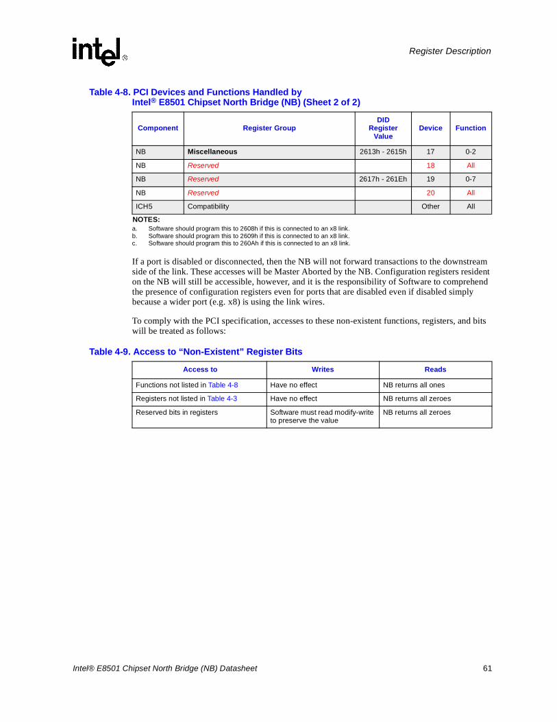
Intel® E8501 Chipset North Bridge (NB) Datasheet 61
Register Description
If a port is disabled or disconnected, then the NB will not forward transactions to the downstream side of the link. These accesses will be Master Aborted by the NB. Configuration registers resident on the NB will still be accessible, however, and it is the responsibility of Software to comprehend the presence of configuration registers even for ports that are disabled even if disabled simply because a wider port (e.g. x8) is using the link wires.
To comply with the PCI specification, accesses to these non-existent functions, registers, and bits will be treated as follows:
NB Miscellaneous 2613h - 2615h 17 0-2
NB Reserved 18 All
NB Reserved 2617h - 261Eh 19 0-7
NB Reserved 20 All
ICH5 Compatibility Other All
NOTES:a. Software should program this to 2608h if this is connected to an x8 link.b. Software should program this to 2609h if this is connected to an x8 link.c. Software should program this to 260Ah if this is connected to an x8 link.
Table 4-8. PCI Devices and Functions Handled by Intel® E8501 Chipset North Bridge (NB) (Sheet 2 of 2)
Component Register GroupDID
Register Value
Device Function
Table 4-9. Access to “Non-Existent” Register Bits
Access to Writes Reads
Functions not listed in Table 4-8 Have no effect NB returns all ones
Registers not listed in Table 4-3 Have no effect NB returns all zeroes
Reserved bits in registers Software must read modify-write to preserve the value
NB returns all zeroes
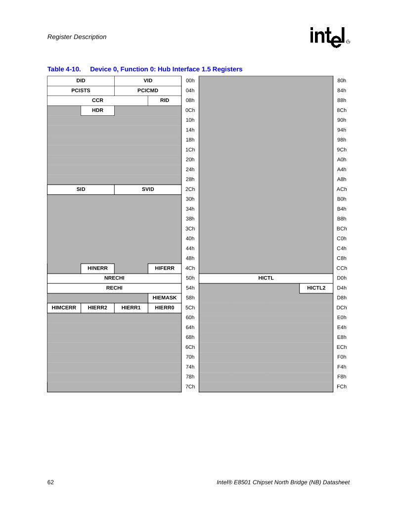
62 Intel® E8501 Chipset North Bridge (NB) Datasheet
Register Description
Table 4-10. Device 0, Function 0: Hub Interface 1.5 RegistersDID VID 00h 80h
PCISTS PCICMD 04h 84h
CCR RID 08h 88h
HDR 0Ch 8Ch
10h 90h
14h 94h
18h 98h
1Ch 9Ch
20h A0h
24h A4h
28h A8h
SID SVID 2Ch ACh
30h B0h
34h B4h
38h B8h
3Ch BCh
40h C0h
44h C4h
48h C8h
HINERR HIFERR 4Ch CCh
NRECHI 50h HICTL D0h
RECHI 54h HICTL2 D4h
HIEMASK 58h D8h
HIMCERR HIERR2 HIERR1 HIERR0 5Ch DCh
60h E0h
64h E4h
68h E8h
6Ch ECh
70h F0h
74h F4h
78h F8h
7Ch FCh
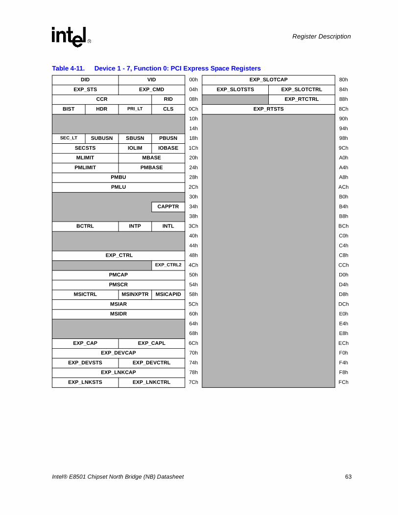
Intel® E8501 Chipset North Bridge (NB) Datasheet 63
Register Description
Table 4-11. Device 1 - 7, Function 0: PCI Express Space RegistersDID VID 00h EXP_SLOTCAP 80h
EXP_STS EXP_CMD 04h EXP_SLOTSTS EXP_SLOTCTRL 84h
CCR RID 08h EXP_RTCTRL 88h
BIST HDR PRI_LT CLS 0Ch EXP_RTSTS 8Ch
10h 90h
14h 94h
SEC_LT SUBUSN SBUSN PBUSN 18h 98h
SECSTS IOLIM IOBASE 1Ch 9Ch
MLIMIT MBASE 20h A0h
PMLIMIT PMBASE 24h A4h
PMBU 28h A8h
PMLU 2Ch ACh
30h B0h
CAPPTR 34h B4h
38h B8h
BCTRL INTP INTL 3Ch BCh
40h C0h
44h C4h
EXP_CTRL 48h C8h
EXP_CTRL2 4Ch CCh
PMCAP 50h D0h
PMSCR 54h D4h
MSICTRL MSINXPTR MSICAPID 58h D8h
MSIAR 5Ch DCh
MSIDR 60h E0h
64h E4h
68h E8h
EXP_CAP EXP_CAPL 6Ch ECh
EXP_DEVCAP 70h F0h
EXP_DEVSTS EXP_DEVCTRL 74h F4h
EXP_LNKCAP 78h F8h
EXP_LNKSTS EXP_LNKCTRL 7Ch FCh
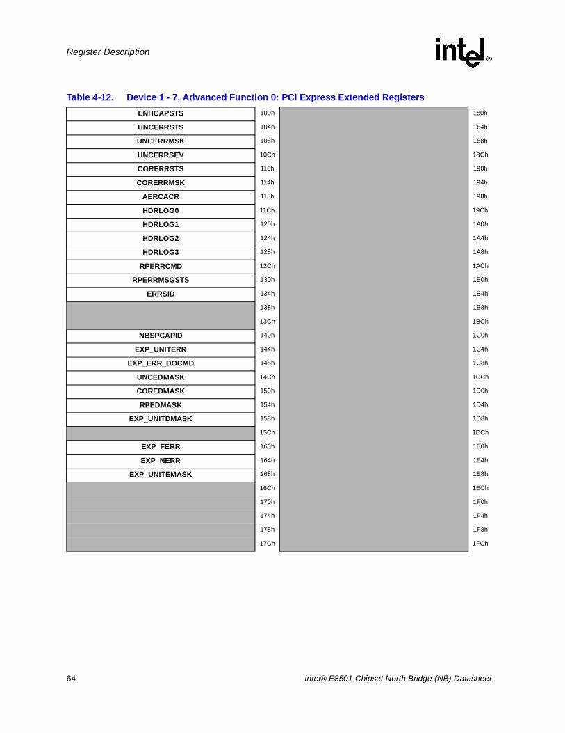
64 Intel® E8501 Chipset North Bridge (NB) Datasheet
Register Description
Table 4-12. Device 1 - 7, Advanced Function 0: PCI Express Extended RegistersENHCAPSTS 100h 180h
UNCERRSTS 104h 184h
UNCERRMSK 108h 188h
UNCERRSEV 10Ch 18Ch
CORERRSTS 110h 190h
CORERRMSK 114h 194h
AERCACR 118h 198h
HDRLOG0 11Ch 19Ch
HDRLOG1 120h 1A0h
HDRLOG2 124h 1A4h
HDRLOG3 128h 1A8h
RPERRCMD 12Ch 1ACh
RPERRMSGSTS 130h 1B0h
ERRSID 134h 1B4h
138h 1B8h
13Ch 1BCh
NBSPCAPID 140h 1C0h
EXP_UNITERR 144h 1C4h
EXP_ERR_DOCMD 148h 1C8h
UNCEDMASK 14Ch 1CCh
COREDMASK 150h 1D0h
RPEDMASK 154h 1D4h
EXP_UNITDMASK 158h 1D8h
15Ch 1DCh
EXP_FERR 160h 1E0h
EXP_NERR 164h 1E4h
EXP_UNITEMASK 168h 1E8h
16Ch 1ECh
170h 1F0h
174h 1F4h
178h 1F8h
17Ch 1FCh
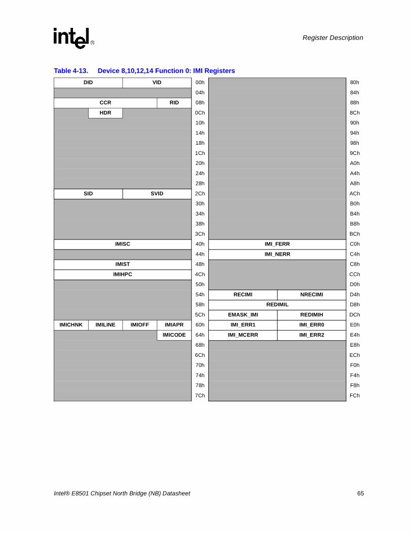
Intel® E8501 Chipset North Bridge (NB) Datasheet 65
Register Description
Table 4-13. Device 8,10,12,14 Function 0: IMI RegistersDID VID 00h 80h
04h 84h
CCR RID 08h 88h
HDR 0Ch 8Ch
10h 90h
14h 94h
18h 98h
1Ch 9Ch
20h A0h
24h A4h
28h A8h
SID SVID 2Ch ACh
30h B0h
34h B4h
38h B8h
3Ch BCh
IMISC 40h IMI_FERR C0h
44h IMI_NERR C4h
IMIST 48h C8h
IMIHPC 4Ch CCh
50h D0h
54h RECIMI NRECIMI D4h
58h REDIMIL D8h
5Ch EMASK_IMI REDIMIH DCh
IMICHNK IMILINE IMIOFF IMIAPR 60h IMI_ERR1 IMI_ERR0 E0h
IMICODE 64h IMI_MCERR IMI_ERR2 E4h
68h E8h
6Ch ECh
70h F0h
74h F4h
78h F8h
7Ch FCh
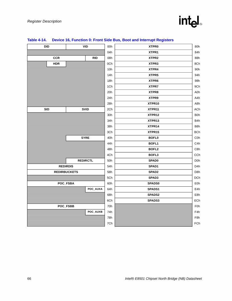
66 Intel® E8501 Chipset North Bridge (NB) Datasheet
Register Description
Table 4-14. Device 16, Function 0: Front Side Bus, Boot and Interrupt RegistersDID VID 00h XTPR0 80h
04h XTPR1 84h
CCR RID 08h XTPR2 88h
HDR 0Ch XTPR3 8Ch
10h XTPR4 90h
14h XTPR5 94h
18h XTPR6 98h
1Ch XTPR7 9Ch
20h XTPR8 A0h
24h XTPR9 A4h
28h XTPR10 A8h
SID SVID 2Ch XTPR11 ACh
30h XTPR12 B0h
34h XTPR13 B4h
38h XTPR14 B8h
3Ch XTPR15 BCh
SYRE 40h BOFL0 C0h
44h BOFL1 C4h
48h BOFL2 C8h
4Ch BOFL3 CCh
REDIRCTL 50h SPAD0 D0h
REDIRDIS 54h SPAD1 D4h
REDIRBUCKETS 58h SPAD2 D8h
5Ch SPAD3 DCh
POC_FSBA 60h SPADS0 E0h
POC_AUXA 64h SPADS1 E4h
68h SPADS2 E8h
6Ch SPADS3 ECh
POC_FSBB 70h F0h
POC_AUXB 74h F4h
78h F8h
7Ch FCh
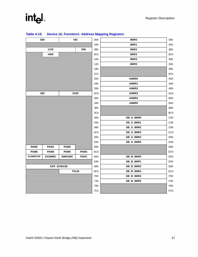
Intel® E8501 Chipset North Bridge (NB) Datasheet 67
Register Description
Table 4-15. Device 16, Function1: Address Mapping RegistersDID VID 00h IMIR0 80h
04h IMIR1 84h
CCR RID 08h IMIR2 88h
HDR 0Ch IMIR3 8Ch
10h IMIR4 90h
14h IMIR5 94h
18h 98h
1Ch 9Ch
20h AIMIR0 A0h
24h AIMIR1 A4h
28h AIMIR2 A8h
SID SVID 2Ch AIMIR3 ACh
30h AIMIR4 B0h
34h AIMIR5 B4h
38h B8h
3Ch BCh
40h SB_A_IMIR0 C0h
44h SB_A_IMIR1 C4h
48h SB_A_IMIR2 C8h
4Ch SB_A_IMIR3 CCh
50h SB_A_IMIR4 D0h
54h SB_A_IMIR5 D4h
PAM2 PAM1 PAM0 58h D8h
PAM6 PAM5 PAM4 PAM3 5Ch DCh
EXSMRTOP EXSMRC SMRAMC FDHC 60h SB_B_IMIR0 E0h
64h SB_B_IMIR1 E4h
EXP_ECBASE 68h SB_B_IMIR2 E8h
TOLM 6Ch SB_B_IMIR3 ECh
70h SB_B_IMIR4 F0h
74h SB_B_IMIR5 F4h
78h F8h
7Ch FCh
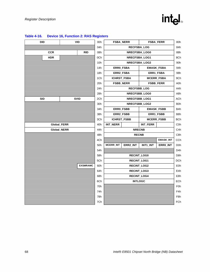
68 Intel® E8501 Chipset North Bridge (NB) Datasheet
Register Description
Table 4-16. Device 16, Function 2: RAS RegistersDID VID 00h FSBA_NERR FSBA_FERR 80h
04h RECFSBA_LOG 84h
CCR RID 08h NRECFSBA_LOG0 88h
HDR 0Ch NRECFSBA_LOG1 8Ch
10h NRECFSBA_LOG2 90h
14h ERR0_FSBA EMASK_FSBA 94h
18h ERR2_FSBA ERR1_FSBA 98h
1Ch ICHRST_FSBA MCERR_FSBA 9Ch
20h FSBB_NERR FSBB_FERR A0h
24h RECFSBB_LOG A4h
28h NRECFSBB_LOG0 A8h
SID SVID 2Ch NRECFSBB_LOG1 ACh
30h NRECFSBB_LOG2 B0h
34h ERR0_FSBB EMASK_FSBB B4h
38h ERR2_FSBB ERR1_FSBB B8h
3Ch ICHRST_FSBB MCERR_FSBB BCh
Global_FERR 40h INT_NERR INT_FERR C0h
Global_NERR 44h NRECNB C4h
48h RECNB C8h
4Ch EMASK_INT CCh
50h MCERR_INT ERR2_INT INT1_INT ERR0_INT D0h
54h D4h
58h RECINT_LOG0 D8h
5Ch RECINT_LOG1 DCh
EXSMRAMC 60h RECINT_LOG2 E0h
64h RECINT_LOG3 E4h
68h RECINT_LOG4 E8h
6Ch INTLOGC ECh
70h F0h
74h F4h
78h F8h
7Ch FCh
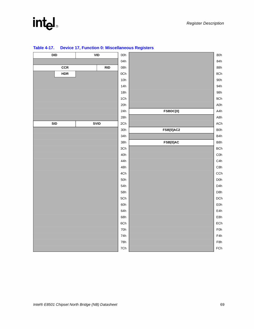
Intel® E8501 Chipset North Bridge (NB) Datasheet 69
Register Description
Table 4-17. Device 17, Function 0: Miscellaneous RegistersDID VID 00h 80h
04h 84h
CCR RID 08h 88h
HDR 0Ch 8Ch
10h 90h
14h 94h
18h 98h
1Ch 9Ch
20h A0h
24h FSBDC[0] A4h
28h A8h
SID SVID 2Ch ACh
30h FSB[0]AC2 B0h
34h B4h
38h FSB[0]AC B8h
3Ch BCh
40h C0h
44h C4h
48h C8h
4Ch CCh
50h D0h
54h D4h
58h D8h
5Ch DCh
60h E0h
64h E4h
68h E8h
6Ch ECh
70h F0h
74h F4h
78h F8h
7Ch FCh
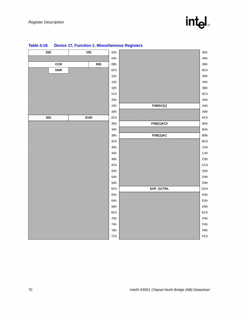
70 Intel® E8501 Chipset North Bridge (NB) Datasheet
Register Description
Table 4-18. Device 17, Function 1: Miscellaneous RegistersDID VID 00h 80h
04h 84h
CCR RID 08h 88h
HDR 0Ch 8Ch
10h 90h
14h 94h
18h 98h
1Ch 9Ch
20h A0h
24h FSBDC[1] A4h
28h A8h
SID SVID 2Ch ACh
30h FSB[1]AC2 B0h
34h B4h
38h FSB[1]AC B8h
3Ch BCh
40h C0h
44h C4h
48h C8h
4Ch CCh
50h D0h
54h D4h
58h D8h
5Ch EXP_GCTRL DCh
60h E0h
64h E4h
68h E8h
6Ch ECh
70h F0h
74h F4h
78h F8h
7Ch FCh
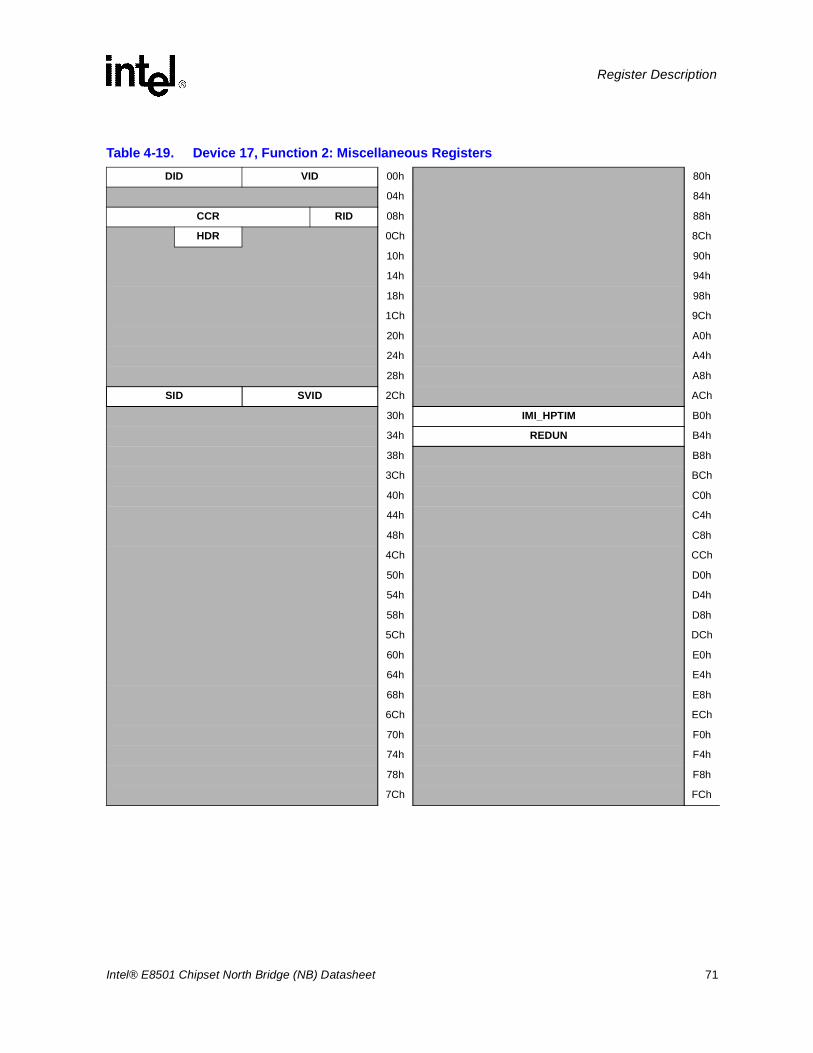
Intel® E8501 Chipset North Bridge (NB) Datasheet 71
Register Description
Table 4-19. Device 17, Function 2: Miscellaneous RegistersDID VID 00h 80h
04h 84h
CCR RID 08h 88h
HDR 0Ch 8Ch
10h 90h
14h 94h
18h 98h
1Ch 9Ch
20h A0h
24h A4h
28h A8h
SID SVID 2Ch ACh
30h IMI_HPTIM B0h
34h REDUN B4h
38h B8h
3Ch BCh
40h C0h
44h C4h
48h C8h
4Ch CCh
50h D0h
54h D4h
58h D8h
5Ch DCh
60h E0h
64h E4h
68h E8h
6Ch ECh
70h F0h
74h F4h
78h F8h
7Ch FCh
72 Intel® E8501 Chipset North Bridge (NB) Datasheet
Register Description
4.10 Hub Interface 1.5 (Device 0, Function 0)The Hub Interface 1.5 (HI1.5) registers are in device 0 (D0), function 0 (F0). For quick reference on the register address map, please refer to Table 4-10.
Warning: Address locations that are not listed are considered reserved locations. Writes to “Reserved” registers may cause unpredictable behavior. Reads to “Reserved” registers may return a non-zero value.
4.10.1 VID: Vendor Identification Register (D0, F0)This register identifies Intel as the manufacturer of the Intel® E8501 chipset North Bridge (NB). Writes to this register have no effect.
4.10.2 DID: Device Identification Register (D0, F0)This register, combined with the Vendor Identification register uniquely, identifies the NB Function in the event that a driver is required. Writes to this register have no effect.
Device 0Function: 0Offset: 00 - 01h
Bit Attr Default Description
15:0 RO 8086h Vendor Identification NumberThe value assigned to Intel.
Device 0Function: 0Offset: 02h - 03h
Bit Attr Default Description
15:0 RO 2600h Device Identification Number Identifies each function of the NB.
Intel® E8501 Chipset North Bridge (NB) Datasheet 73
Register Description
4.10.3 PCICMD:PCI Command Register (D0, F0)
4.10.4 PCISTS: PCI Status Register (D0, F0)
Device: 0Function: 0Offset: 04h
Bit Attr Default Description
15:9 RV 00h Reserved
8 RO 0 SIG_SYS_ERR: Signalled System Error.The NB never initiates a system error special cycle (DO_SERR), so this bit will always return a 0 when read.
7 RV 0b Reserved
6 RWST 0 IERRE: Parity Error Response (IERRE).Controls the NB response when a parity error (on function 0) or multi-bit ECC error is detected on the Hub Interface. This bit only controls the detection in PCISTS.DetIntErr and PCISTS.MstrDataIE.The NB reports all parity errors on the Hub Interface.
5:4 RV 00b Reserved
3 RO 0b spec_cyc_en: Special Cycle Enable.Controls the ability to forward PCI-type (legacy) special cycles. Devices on the Hub Interface are not capable of accepting legacy special cycles. This bit does not apply to Hub Interface specific special cycles.
2 RO 1b BM_en: Bus Master Enable.Controls the ability for the NB to initiate Hub Interface cycles. The NB can always issue Hub Interface bus cycles.
1 RO 1b MemAccEn: Memory Access Enable.Controls the ability for the NB to respond to memory transactions initiated on the Hub Interface. The NB can always accept memory transactions.
0 RO 0b IOAccEn: I/O Access Enable.Controls the ability for the NB to respond to I/O transactions initiated on the Hub Interface. This chipset does not support inbound I/O cycles.
Device: 0Function: 0Offset: 06h - 07h
Bit Attr Default Description
15 RWC 0 DetIntErr: Detected Integrity ErrorThis bit indicates that a parity error was observed on the Hub Interface. This bit is not affected by the state of PCICMD.IERR.
14 RO 0 SSE: Signalled System ErrorThis bit indicates if a system error special cycle (DO_SERR) is initiated by the NB component. This bit should never be asserted since the NB never initiates DO_SERR.
13 RWC 0 RcvMstrAbSts: Received Master Abort StatusThis bit indicates if the NB receives a Master Abort completion cycle or an un-implemented Special Cycle command.
74 Intel® E8501 Chipset North Bridge (NB) Datasheet
Register Description
4.10.5 RID: Revision Identification Register (D0, F0)This register contains the revision number of the Intel® E8501 chipset North Bridge (NB).
Intel® E8501 chipset North Bridge (NB) implements the Revision Identification Registers with a Compatibility Revision Id function in addition to standard revision identification functionality. This Compatibility Revision Id functionality is present in order to allow vendors to replace hardware while maintaining the software visible hardware revision identification registers the same as in previous steppings of the NB.
In order to access the Compatibility Revision Id functionality, the RID registers as a whole can be written to exactly one time with a specific code value (key). This key, when written correctly as the first write to any of the RID registers inside NB will cause NB to return the compatibility id value for all future reads of any NB RID register. Table 4-20 describes this compatibility revision identification functionality.
12 RWC 0 RcvTgtAbSts: Received Target Abort StatusThis bit indicates if the NB receives a Target Abort completion cycle in response to a NB-initiated Hub Interface cycle.
11 RWC 0 SigTgtAbSts: Signalled Target Abort StatusThe NB sets this bit when it issues a Target Abort completion cycle to the Hub Interface agent.
10:9 RV 00h Reserved
8 RWC 0 MstrDataIE: Master Data Integrity ErrorThis bit indicates that a data parity or multi-bit ECC error was detected on the Hub Interface. This bit is set when all of the following conditions are met:
• The NB detected a data parity for an outbound read completion• PCICMD.IERR is set to 1
7:0 RV 00h Reserved
Device: 0Function: 0Offset: 06h - 07h
Bit Attr Default Description
Table 4-20. Intel® E8501 Chipset North Bridge (NB) Compatibility Revision ID Function
Key value written to any RID register B0 read value Description
0x79 0x0 Return compatibility id
Any other value 0x10 Return stepping id
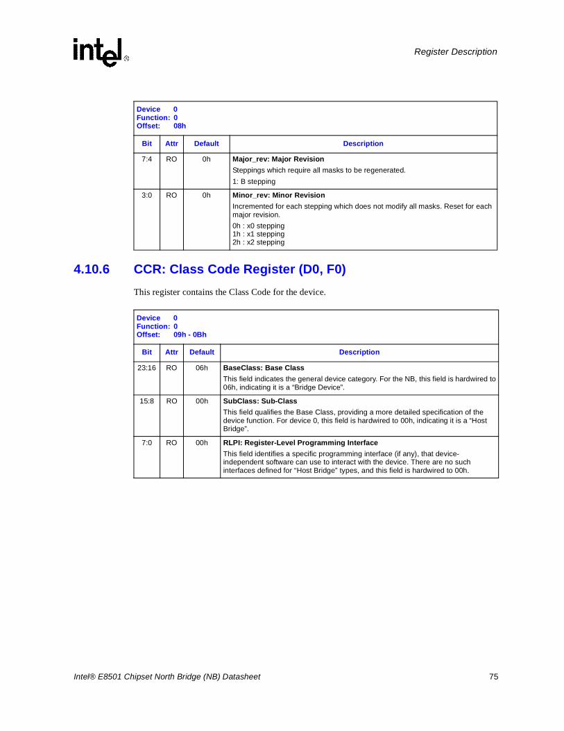
Intel® E8501 Chipset North Bridge (NB) Datasheet 75
Register Description
4.10.6 CCR: Class Code Register (D0, F0)This register contains the Class Code for the device.
Device 0Function: 0Offset: 08h
Bit Attr Default Description
7:4 RO 0h Major_rev: Major RevisionSteppings which require all masks to be regenerated.1: B stepping
3:0 RO 0h Minor_rev: Minor RevisionIncremented for each stepping which does not modify all masks. Reset for each major revision.0h : x0 stepping1h : x1 stepping2h : x2 stepping
Device 0Function: 0Offset: 09h - 0Bh
Bit Attr Default Description
23:16 RO 06h BaseClass: Base ClassThis field indicates the general device category. For the NB, this field is hardwired to06h, indicating it is a “Bridge Device”.
15:8 RO 00h SubClass: Sub-ClassThis field qualifies the Base Class, providing a more detailed specification of the device function. For device 0, this field is hardwired to 00h, indicating it is a “Host Bridge”.
7:0 RO 00h RLPI: Register-Level Programming InterfaceThis field identifies a specific programming interface (if any), that device-independent software can use to interact with the device. There are no such interfaces defined for “Host Bridge” types, and this field is hardwired to 00h.
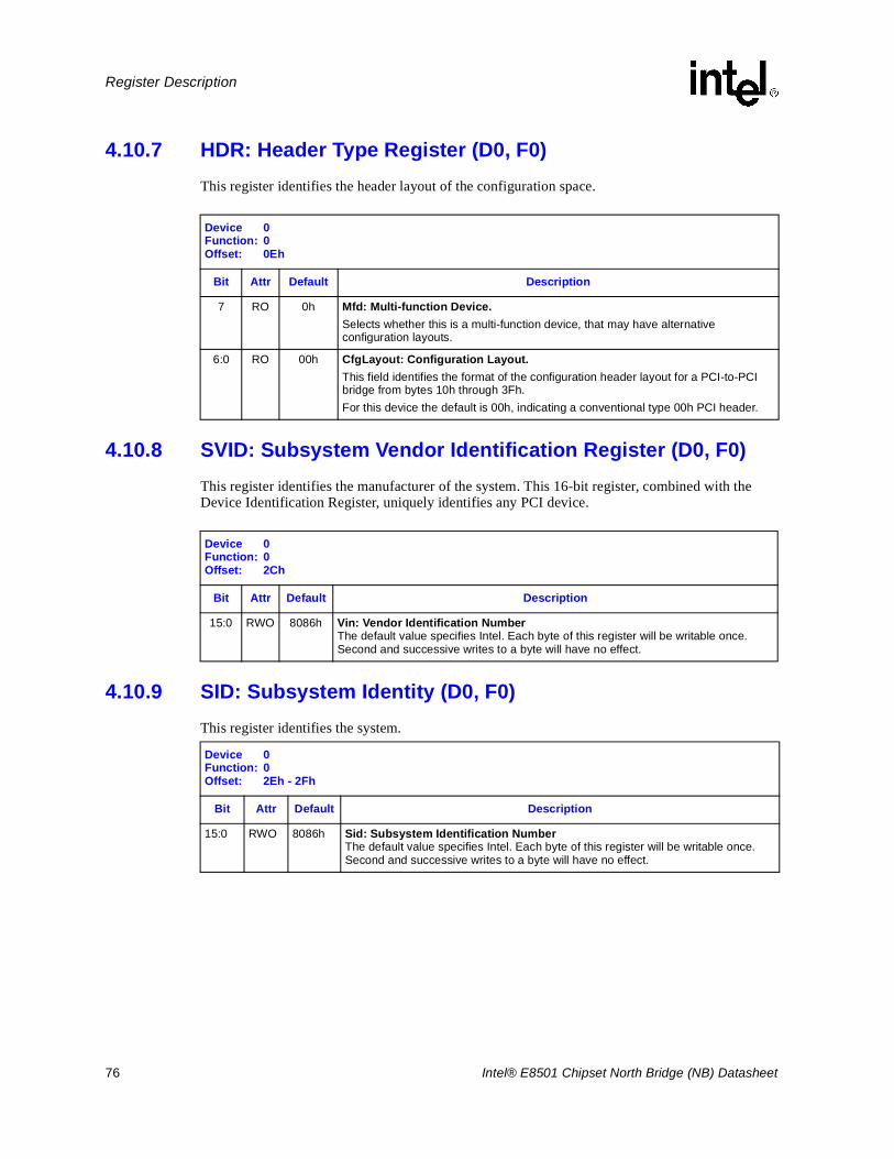
76 Intel® E8501 Chipset North Bridge (NB) Datasheet
Register Description
4.10.7 HDR: Header Type Register (D0, F0)This register identifies the header layout of the configuration space.
4.10.8 SVID: Subsystem Vendor Identification Register (D0, F0)This register identifies the manufacturer of the system. This 16-bit register, combined with the Device Identification Register, uniquely identifies any PCI device.
4.10.9 SID: Subsystem Identity (D0, F0)This register identifies the system.
Device 0Function: 0Offset: 0Eh
Bit Attr Default Description
7 RO 0h Mfd: Multi-function Device.Selects whether this is a multi-function device, that may have alternative configuration layouts.
6:0 RO 00h CfgLayout: Configuration Layout.This field identifies the format of the configuration header layout for a PCI-to-PCI bridge from bytes 10h through 3Fh. For this device the default is 00h, indicating a conventional type 00h PCI header.
Device 0Function: 0Offset: 2Ch
Bit Attr Default Description
15:0 RWO 8086h Vin: Vendor Identification NumberThe default value specifies Intel. Each byte of this register will be writable once. Second and successive writes to a byte will have no effect.
Device 0Function: 0Offset: 2Eh - 2Fh
Bit Attr Default Description
15:0 RWO 8086h Sid: Subsystem Identification Number The default value specifies Intel. Each byte of this register will be writable once. Second and successive writes to a byte will have no effect.
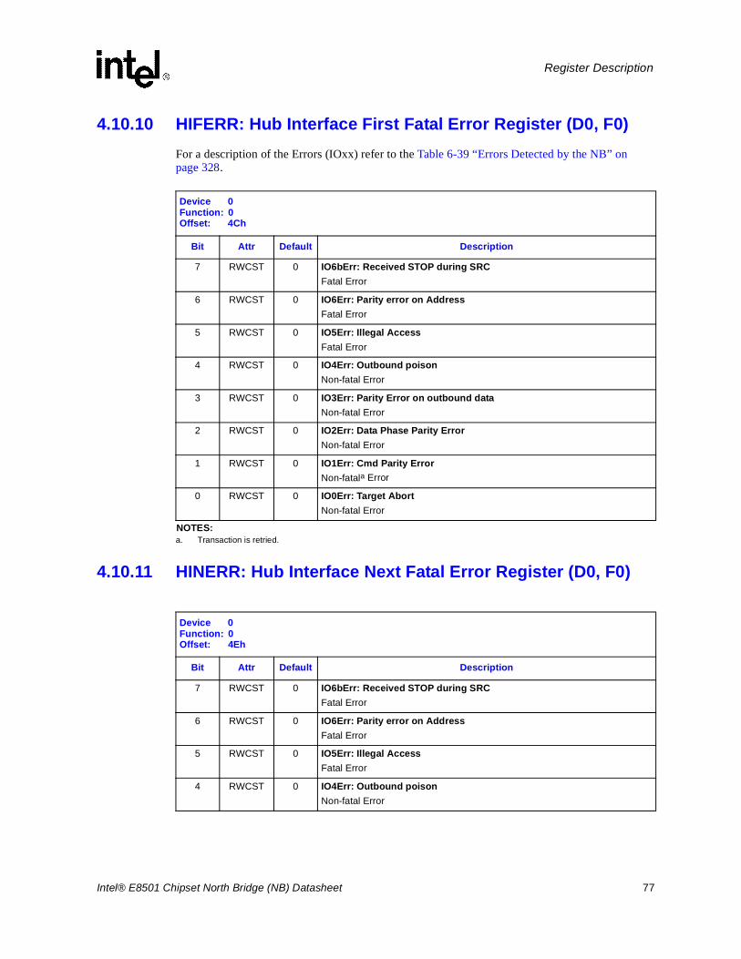
Intel® E8501 Chipset North Bridge (NB) Datasheet 77
Register Description
4.10.10 HIFERR: Hub Interface First Fatal Error Register (D0, F0)For a description of the Errors (IOxx) refer to the Table 6-39 “Errors Detected by the NB” on page 328.
4.10.11 HINERR: Hub Interface Next Fatal Error Register (D0, F0)
Device 0Function: 0Offset: 4Ch
Bit Attr Default Description
7 RWCST 0 IO6bErr: Received STOP during SRCFatal Error
6 RWCST 0 IO6Err: Parity error on AddressFatal Error
5 RWCST 0 IO5Err: Illegal AccessFatal Error
4 RWCST 0 IO4Err: Outbound poisonNon-fatal Error
3 RWCST 0 IO3Err: Parity Error on outbound dataNon-fatal Error
2 RWCST 0 IO2Err: Data Phase Parity ErrorNon-fatal Error
1 RWCST 0 IO1Err: Cmd Parity ErrorNon-fatala Error
NOTES:a. Transaction is retried.
0 RWCST 0 IO0Err: Target AbortNon-fatal Error
Device 0Function: 0Offset: 4Eh
Bit Attr Default Description
7 RWCST 0 IO6bErr: Received STOP during SRCFatal Error
6 RWCST 0 IO6Err: Parity error on AddressFatal Error
5 RWCST 0 IO5Err: Illegal AccessFatal Error
4 RWCST 0 IO4Err: Outbound poisonNon-fatal Error
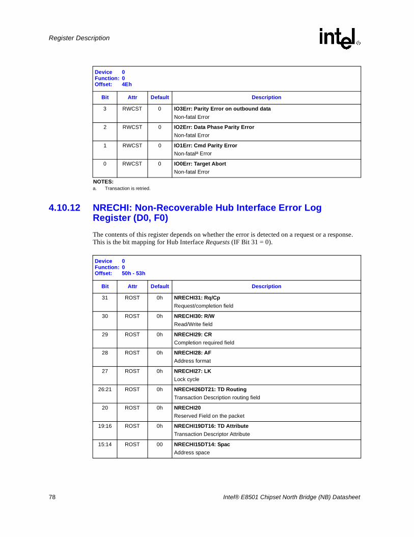
78 Intel® E8501 Chipset North Bridge (NB) Datasheet
Register Description
4.10.12 NRECHI: Non-Recoverable Hub Interface Error LogRegister (D0, F0)The contents of this register depends on whether the error is detected on a request or a response. This is the bit mapping for Hub Interface Requests (IF Bit 31 = 0).
3 RWCST 0 IO3Err: Parity Error on outbound dataNon-fatal Error
2 RWCST 0 IO2Err: Data Phase Parity ErrorNon-fatal Error
1 RWCST 0 IO1Err: Cmd Parity ErrorNon-fatala Error
0 RWCST 0 IO0Err: Target AbortNon-fatal Error
NOTES:a. Transaction is retried.
Device 0Function: 0Offset: 4Eh
Bit Attr Default Description
Device 0Function: 0Offset: 50h - 53h
Bit Attr Default Description
31 ROST 0h NRECHI31: Rq/CpRequest/completion field
30 ROST 0h NRECHI30: R/WRead/Write field
29 ROST 0h NRECHI29: CRCompletion required field
28 ROST 0h NRECHI28: AFAddress format
27 ROST 0h NRECHI27: LKLock cycle
26:21 ROST 0h NRECHI26DT21: TD RoutingTransaction Description routing field
20 ROST 0h NRECHI20Reserved Field on the packet
19:16 ROST 0h NRECHI19DT16: TD AttributeTransaction Descriptor Attribute
15:14 ROST 00 NRECHI15DT14: SpacAddress space
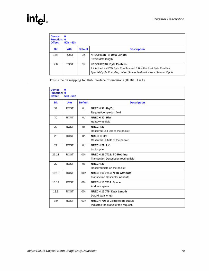
Intel® E8501 Chipset North Bridge (NB) Datasheet 79
Register Description
This is the bit mapping for Hub Interface Completions (IF Bit 31 = 1).:
13:8 ROST 0h NRECHI13DT8: Data LengthDword data length
7:0 ROST 0h NRECHI7DT0: Byte Enables7:4 is the Last DW Byte Enables and 3:0 is the First Byte EnablesSpecial Cycle Encoding: when Space field indicates a Special Cycle
Device 0Function: 0Offset: 50h - 53h
Bit Attr Default Description
Device 0Function: 0Offset: 50h - 53h
Bit Attr Default Description
31 ROST 0b NRECHI31: Rq/CpRequest/completion field
30 ROST 0b NRECHI30: R/WRead/Write field
29 ROST 0b NRECHI29Reserved 1b Field of the packet
28 ROST 0b NRECHIHI28Reserved 1a field of the packet
27 ROST 0b NRECHI27: LKLock cycle
26:21 ROST 00h NRECHI26DT21: TD RoutingTransaction Description routing field
20 ROST 0b NRECHI20Reserved field on the packet
19:16 ROST 00h NRECHI19DT16: N TD AttributeTransaction Descriptor Attribute
15:14 ROST 00h NRECHI15DT14: SpaceAddress space
13:8 ROST 00h NRECHI13DT8: Data LengthDword data length
7:0 ROST 00h NRECHI7DT0: Completion StatusIndicates the status of the request.
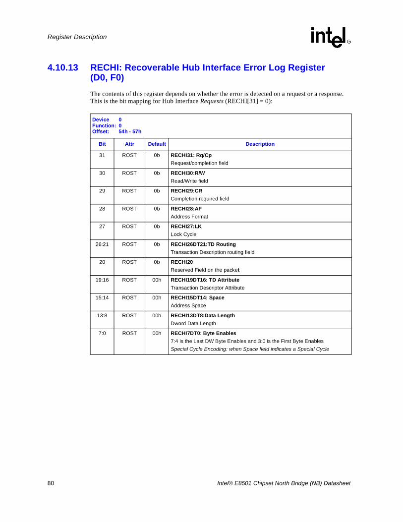
80 Intel® E8501 Chipset North Bridge (NB) Datasheet
Register Description
4.10.13 RECHI: Recoverable Hub Interface Error Log Register (D0, F0) The contents of this register depends on whether the error is detected on a request or a response. This is the bit mapping for Hub Interface Requests (RECHI[31] = 0):
Device 0Function: 0Offset: 54h - 57h
Bit Attr Default Description
31 ROST 0b RECHI31: Rq/CpRequest/completion field
30 ROST 0b RECHI30:R/WRead/Write field
29 ROST 0b RECHI29:CRCompletion required field
28 ROST 0b RECHI28:AFAddress Format
27 ROST 0b RECHI27:LKLock Cycle
26:21 ROST 0b RECHI26DT21:TD RoutingTransaction Description routing field
20 ROST 0b RECHI20Reserved Field on the packet
19:16 ROST 00h RECHI19DT16: TD AttributeTransaction Descriptor Attribute
15:14 ROST 00h RECHI15DT14: SpaceAddress Space
13:8 ROST 00h RECHI13DT8:Data LengthDword Data Length
7:0 ROST 00h RECHI7DT0: Byte Enables7:4 is the Last DW Byte Enables and 3:0 is the First Byte EnablesSpecial Cycle Encoding: when Space field indicates a Special Cycle
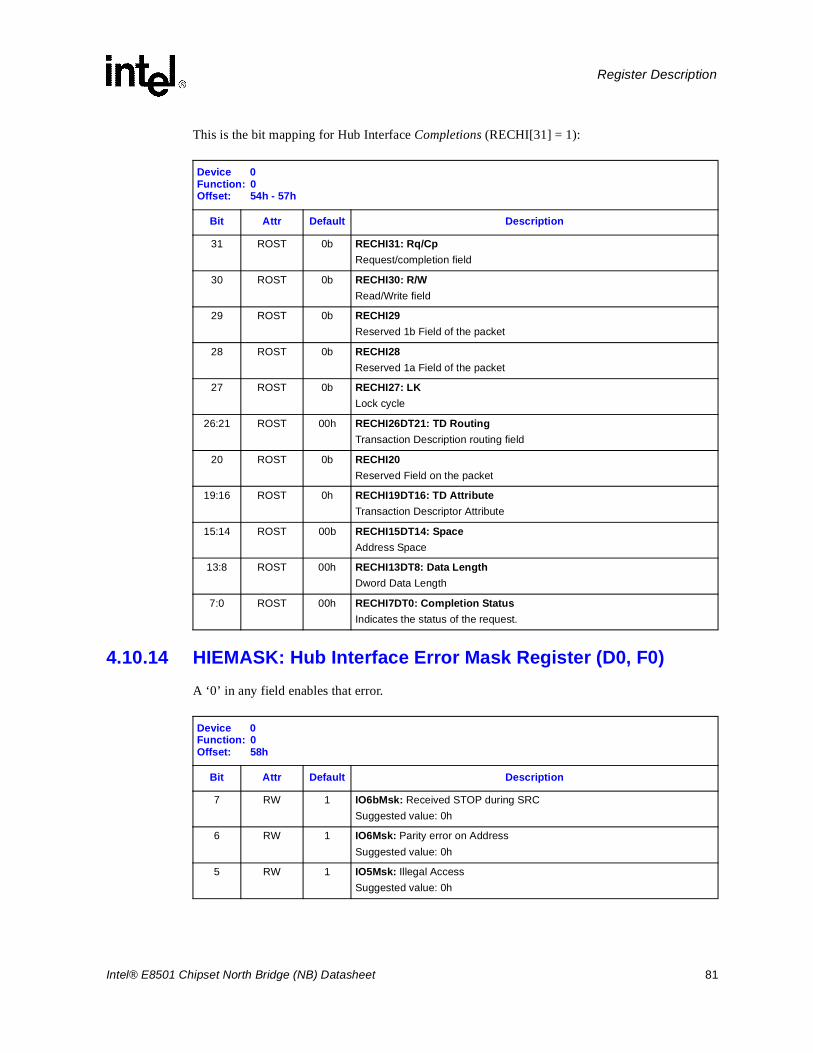
Intel® E8501 Chipset North Bridge (NB) Datasheet 81
Register Description
This is the bit mapping for Hub Interface Completions (RECHI[31] = 1):
4.10.14 HIEMASK: Hub Interface Error Mask Register (D0, F0)A ‘0’ in any field enables that error.
Device 0Function: 0Offset: 54h - 57h
Bit Attr Default Description
31 ROST 0b RECHI31: Rq/CpRequest/completion field
30 ROST 0b RECHI30: R/WRead/Write field
29 ROST 0b RECHI29Reserved 1b Field of the packet
28 ROST 0b RECHI28Reserved 1a Field of the packet
27 ROST 0b RECHI27: LKLock cycle
26:21 ROST 00h RECHI26DT21: TD RoutingTransaction Description routing field
20 ROST 0b RECHI20Reserved Field on the packet
19:16 ROST 0h RECHI19DT16: TD AttributeTransaction Descriptor Attribute
15:14 ROST 00b RECHI15DT14: SpaceAddress Space
13:8 ROST 00h RECHI13DT8: Data LengthDword Data Length
7:0 ROST 00h RECHI7DT0: Completion StatusIndicates the status of the request.
Device 0Function: 0Offset: 58h
Bit Attr Default Description
7 RW 1 IO6bMsk: Received STOP during SRCSuggested value: 0h
6 RW 1 IO6Msk: Parity error on AddressSuggested value: 0h
5 RW 1 IO5Msk: Illegal AccessSuggested value: 0h
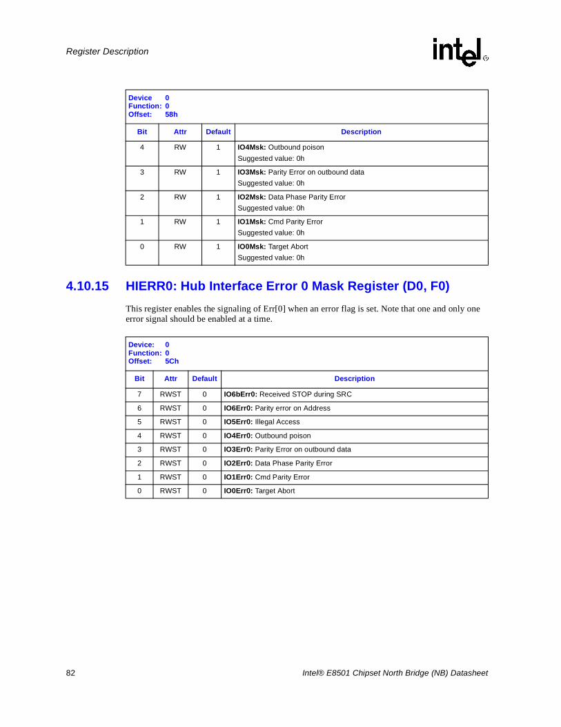
82 Intel® E8501 Chipset North Bridge (NB) Datasheet
Register Description
4.10.15 HIERR0: Hub Interface Error 0 Mask Register (D0, F0)This register enables the signaling of Err[0] when an error flag is set. Note that one and only one error signal should be enabled at a time.
4 RW 1 IO4Msk: Outbound poisonSuggested value: 0h
3 RW 1 IO3Msk: Parity Error on outbound dataSuggested value: 0h
2 RW 1 IO2Msk: Data Phase Parity ErrorSuggested value: 0h
1 RW 1 IO1Msk: Cmd Parity ErrorSuggested value: 0h
0 RW 1 IO0Msk: Target AbortSuggested value: 0h
Device 0Function: 0Offset: 58h
Bit Attr Default Description
Device: 0Function: 0Offset: 5Ch
Bit Attr Default Description
7 RWST 0 IO6bErr0: Received STOP during SRC
6 RWST 0 IO6Err0: Parity error on Address
5 RWST 0 IO5Err0: Illegal Access
4 RWST 0 IO4Err0: Outbound poison
3 RWST 0 IO3Err0: Parity Error on outbound data
2 RWST 0 IO2Err0: Data Phase Parity Error
1 RWST 0 IO1Err0: Cmd Parity Error
0 RWST 0 IO0Err0: Target Abort
Intel® E8501 Chipset North Bridge (NB) Datasheet 83
Register Description
4.10.16 HIERR1: Hub Interface Error 1 Mask Register (D0, F0)This register enables the signaling of Err[1] when an error flag is set. Note that one and only one error signal should be enabled at a time.
4.10.17 HIERR2: Hub Interface Error 2 Mask Register (D0, F0)This register enables the signaling of Err[2] when an error flag is set. Note that one and only one error signal should be enabled at a time.
Device: 0Function: 0Offset: 5Dh
Bit Attr Default Description
7 RWST 0 IO6bErr1: Received STOP during SRC
6 RWST 0 IO6Err1: Parity error on Address
5 RWST 0 IO5Err1: Illegal Access
4 RWST 0 IO4Err1: Outbound poison
3 RWST 0 IO3Err1: Parity Error on outbound data
2 RWST 0 IO2Err1: Data Phase Parity Error
1 RWST 0 IO1Err1: Cmd Parity Error
0 RWST 0 IO0Err1: Target Abort
Device: 0Function: 0Offset: 5Eh
Bit Attr Default Description
7 RWST 0 IO6bErr2: Received STOP during SRC
6 RWST 0 IO6Err2: Parity error on Address
5 RWST 0 IO5Err2: Illegal Access
4 RWST 0 IO4Err2: Outbound poison
3 RWST 0 IO3Err2: Parity Error on outbound data
2 RWST 0 IO2Err2: Data Phase Parity Error
1 RWST 0 IO1Err2: Cmd Parity Error
0 RWST 0 IO0Err2: Target Abort
84 Intel® E8501 Chipset North Bridge (NB) Datasheet
Register Description
4.10.18 HIMCERR: Hub Interface MCERR Mask Register (D0, F0)This register enables the signaling of MCERR when an error flag is set. Note that one and only one error signal should be enabled at a time.
4.10.19 HICTL: Hub Interface Command Control Register (D0, F0)
Device: 0Function: 0Offset: 5Fh
Bit Attr Default Description
7 RWST 0 IO6bMCErr: Received STOP during SRC
6 RWST 0 IO6MCErr: Parity error on Address
5 RWST 0 IO5MCErr: Illegal Access
4 RWST 0 IO4MCErr: Outbound poison
3 RWST 0 IO3MCErr: Parity Error on outbound data
2 RWST 0 IO2MCErr: Data Phase Parity ErrorSuggested value: 1h
1 RWST 0 IO1MCErr: Cmd Parity Error
0 RWST 0 IO0MCErr: Target Abort
Device: 0Function: 0Offset: D0h - D3h
Bit Attr Default Description
31:29 RO 0h HUB_SUB_FIRST: This field stores the lowest subordinate Hub Interface hub number. This information is compared with the Hub ID to determine whether a completion packet should be forwarded further down the Hub Interface hierarchy.
28 RV 0h Reserved
27:25 RO 0h HUB_SUB_LAST: This field stores the highest subordinate Hub Interface hub number. This information is compared with the Hub ID to determine whether a completion packet should be forwarded further down the Hub Interface hierarchy.
24 RV 0h Reserved
23:21 RO 0h HUB_ID: This field identifies the Hub Interface ID number for the NB. The NB uses this field to determine when to accept a Hub Interface request packet and send any corresponding completion packets.
20 RV 0 Reserved
19:16 RW 0h HI_TIMESLICE: This field sets the Hub Interface arbiter time-slice value with four base-clock granularity. A value of zero means that the timer immediately expires and the NB will allow the agent interfacing Hub Interface access to the bus every other transaction.
15:14 RO 0h HI_WIDTH: This field sets the Hub Interface data bus width. A value of 01 indicates a 16-bit data bus and 00 indicates an 8-bit data bus.
Intel® E8501 Chipset North Bridge (NB) Datasheet 85
Register Description
13 RO 1h HI_RATE_VALID: This bit is sampled by software and indicates when the Hub Interface bus rate is valid.
12:10 RO 010b HI_RATE: This field indicates the Hub Interface data rate. Function 0 only supports a 4x data rate encoded with 010.
9:8 RW 0h RCOMP_INT: Determines the time interval for impedance compensation. Encodings are:
7:5 RV 0h Reserved
4 RWO 0 DIS_INB_CFG: Disable Inbound ConfigsThis bit is used for controlling configuration accesses to the chipset registers through the Hub Interface.
This register bit is of type “write once” and is controlled by BIOS/special initialization firmware.
3:1 RO 001 MAX_DATA: This field is programmed with the longest data stream the NB is permitted to send on the Hub Interface. MAX_DATA applies to both write request cycles and read completion cycles.
0 RV 0 EN64: Enable 64 bit AddressingThe NB does not support 64-bit addressing on the Hub Interface
Device: 0Function: 0Offset: D0h - D3h
Bit Attr Default Description
00: 128 ms
01: 250 µs
10: 16 ms
11: 2 ms
0: Allows access to the NB or XMB registers.
1: Inbound accesses to the NB or XMB registers will be dropped and logged as an illegal access.
000: 32 bytes
001: 64 bytes
01X: 128 bytes
1XX: 256 bytes
86 Intel® E8501 Chipset North Bridge (NB) Datasheet
Register Description
4.10.20 HICTL2: Hub Interface Command Control Register (D0, F0)
4.11 PCI Express Ports (Device 1 - 7, Function 0)The PCI Express registers are in Device 1 - 7 (D1-7), Function 0 (F0). For the register address map, please refer to Table 4-11. The following registers define the standard PCI 2.3 compatible and extended PCI Express configuration space for each of the PCI Express x4 links in the NB. Unless otherwise specified, the registers are enumerated as a vector [7:1] mapping to each of the seven PCI Express ports uniquely.
Warning: Address locations that are not listed are considered reserved locations. Writes to “Reserved” registers may cause unpredictable behavior. Reads to “Reserved” registers may return a non-zero value.
4.11.1 VID[7:1]: Vendor Identification Register (D1-7, F0)The VID Register contains Intel as the manufacturer of the NB. Writes to this register have no effect.
4.11.2 DID[7:1]: Device Identification Register (D1-7, F0)This register combined with the Vendor Identification register uniquely identifies the NB function in the event that a driver is required. Writes to this register have no effect.
Device: 0Function: 0Offset: D4h
Bit Attr Default Description
7:5 RV 0 Reserved
4:0 RW 0 STOPGRANTACKCNT:The NB will forward every (N+1)th StopGrantAck to the Hub Interface. The default provides for every StopGrantAck to be sent to the Hub Interface. Software is expected to set this to a value of THREADs-1 where THREAD is the number of threads that will issue a StopGrantAck in response to a StopClock request.
Device: 1 - 7Function: 0Offset: 00 - 01h
Bit Attr Default Description
15:0 RO 8086h Vendor Identification NumberThe value is assigned to Intel’s standard notation.
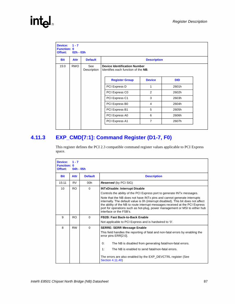
Intel® E8501 Chipset North Bridge (NB) Datasheet 87
Register Description
4.11.3 EXP_CMD[7:1]: Command Register (D1-7, F0)This register defines the PCI 2.3 compatible command register values applicable to PCI Express space.
Device: 1 - 7Function: 0Offset: 02h - 03h
Bit Attr Default Description
15:0 RWO See Description
Device Identification Number Identifies each function of the NB.
Register Group Device DID
PCI Express D 1 2601h
PCI Express C0 2 2602h
PCI Express C1 3 2603h
PCI Express B0 4 2604h
PCI Express B1 5 2605h
PCI Express A0 6 2606h
PCI Express A1 7 2607h
Device: 1 - 7 Function: 0Offset: 04h - 05h
Bit Attr Default Description
15:11 RV 00h Reserved (by PCI SIG)
10 RO 0 INTxDisable: Interrupt DisableControls the ability of the PCI Express port to generate INTx messages.Note that the NB does not have INTx pins and cannot generate interrupts internally. The default value is 0h (interrupt disabled). This bit does not affect the ability of the NB to route interrupt messages received at the PCI Express port for operations such as hot-plug, power management or MSI to either hub interface or the FSB’s.
9 RO 0 FB2B: Fast Back-to-Back EnableNot applicable to PCI Express and is hardwired to ‘0’.
8 RW 0 SERRE: SERR Message EnableThis field handles the reporting of fatal and non-fatal errors by enabling the error pins ERR[2:0].
The errors are also enabled by the EXP_DEVCTRL register (See Section 4.11.40)
0: The NB is disabled from generating fatal/non-fatal errors.
1: The NB is enabled to send fatal/non-fatal errors.
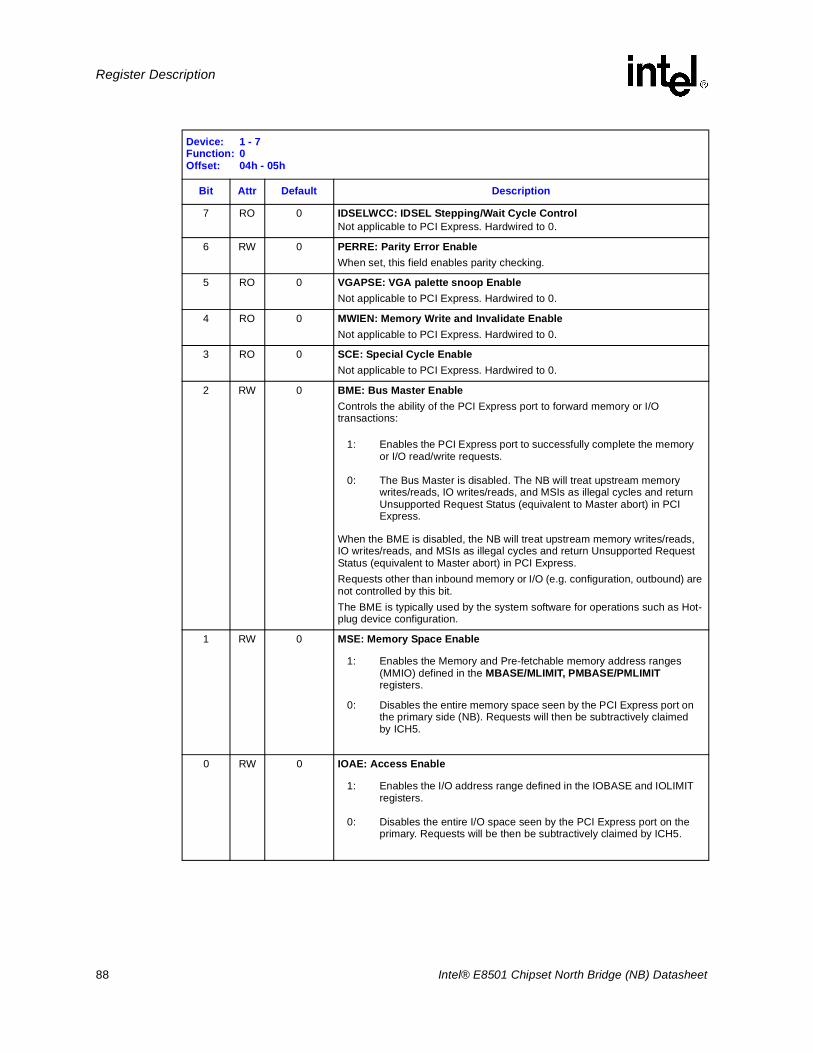
88 Intel® E8501 Chipset North Bridge (NB) Datasheet
Register Description
7 RO 0 IDSELWCC: IDSEL Stepping/Wait Cycle ControlNot applicable to PCI Express. Hardwired to 0.
6 RW 0 PERRE: Parity Error Enable When set, this field enables parity checking.
5 RO 0 VGAPSE: VGA palette snoop EnableNot applicable to PCI Express. Hardwired to 0.
4 RO 0 MWIEN: Memory Write and Invalidate EnableNot applicable to PCI Express. Hardwired to 0.
3 RO 0 SCE: Special Cycle EnableNot applicable to PCI Express. Hardwired to 0.
2 RW 0 BME: Bus Master EnableControls the ability of the PCI Express port to forward memory or I/O transactions:
When the BME is disabled, the NB will treat upstream memory writes/reads, IO writes/reads, and MSIs as illegal cycles and return Unsupported Request Status (equivalent to Master abort) in PCI Express.Requests other than inbound memory or I/O (e.g. configuration, outbound) are not controlled by this bit.The BME is typically used by the system software for operations such as Hot-plug device configuration.
1 RW 0 MSE: Memory Space Enable
0 RW 0 IOAE: Access Enable
Device: 1 - 7 Function: 0Offset: 04h - 05h
Bit Attr Default Description
1: Enables the PCI Express port to successfully complete the memory or I/O read/write requests.
0: The Bus Master is disabled. The NB will treat upstream memory writes/reads, IO writes/reads, and MSIs as illegal cycles and return Unsupported Request Status (equivalent to Master abort) in PCI Express.
1: Enables the Memory and Pre-fetchable memory address ranges (MMIO) defined in the MBASE/MLIMIT, PMBASE/PMLIMITregisters.
0: Disables the entire memory space seen by the PCI Express port on the primary side (NB). Requests will then be subtractively claimed by ICH5.
1: Enables the I/O address range defined in the IOBASE and IOLIMIT registers.
0: Disables the entire I/O space seen by the PCI Express port on the primary. Requests will be then be subtractively claimed by ICH5.
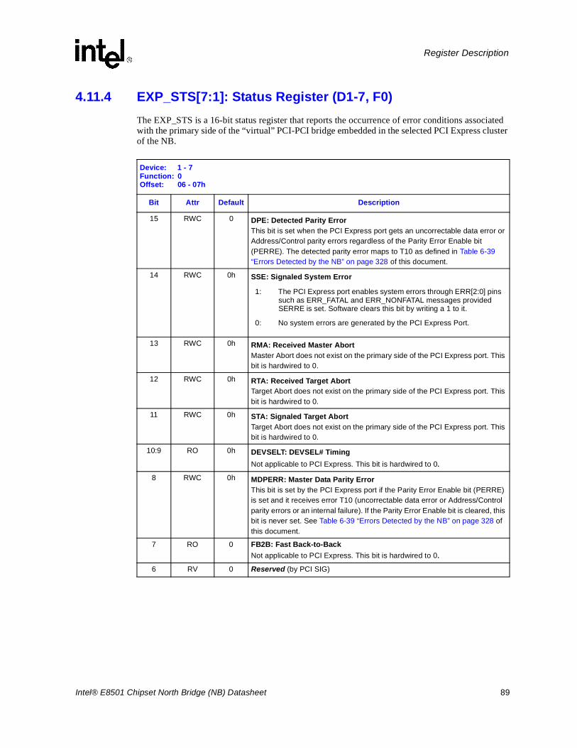
Intel® E8501 Chipset North Bridge (NB) Datasheet 89
Register Description
4.11.4 EXP_STS[7:1]: Status Register (D1-7, F0)The EXP_STS is a 16-bit status register that reports the occurrence of error conditions associated with the primary side of the “virtual” PCI-PCI bridge embedded in the selected PCI Express cluster of the NB.
Device: 1 - 7Function: 0Offset: 06 - 07h
Bit Attr Default Description
15 RWC 0 DPE: Detected Parity ErrorThis bit is set when the PCI Express port gets an uncorrectable data error or Address/Control parity errors regardless of the Parity Error Enable bit (PERRE). The detected parity error maps to T10 as defined in Table 6-39 “Errors Detected by the NB” on page 328 of this document.
14 RWC 0h SSE: Signaled System Error
13 RWC 0h RMA: Received Master AbortMaster Abort does not exist on the primary side of the PCI Express port. This bit is hardwired to 0.
12 RWC 0h RTA: Received Target AbortTarget Abort does not exist on the primary side of the PCI Express port. This bit is hardwired to 0.
11 RWC 0h STA: Signaled Target AbortTarget Abort does not exist on the primary side of the PCI Express port. This bit is hardwired to 0.
10:9 RO 0h DEVSELT: DEVSEL# TimingNot applicable to PCI Express. This bit is hardwired to 0.
8 RWC 0h MDPERR: Master Data Parity ErrorThis bit is set by the PCI Express port if the Parity Error Enable bit (PERRE) is set and it receives error T10 (uncorrectable data error or Address/Control parity errors or an internal failure). If the Parity Error Enable bit is cleared, this bit is never set. See Table 6-39 “Errors Detected by the NB” on page 328 of this document.
7 RO 0 FB2B: Fast Back-to-BackNot applicable to PCI Express. This bit is hardwired to 0.
6 RV 0 Reserved (by PCI SIG)
1: The PCI Express port enables system errors through ERR[2:0] pins such as ERR_FATAL and ERR_NONFATAL messages provided SERRE is set. Software clears this bit by writing a 1 to it.
0: No system errors are generated by the PCI Express Port.
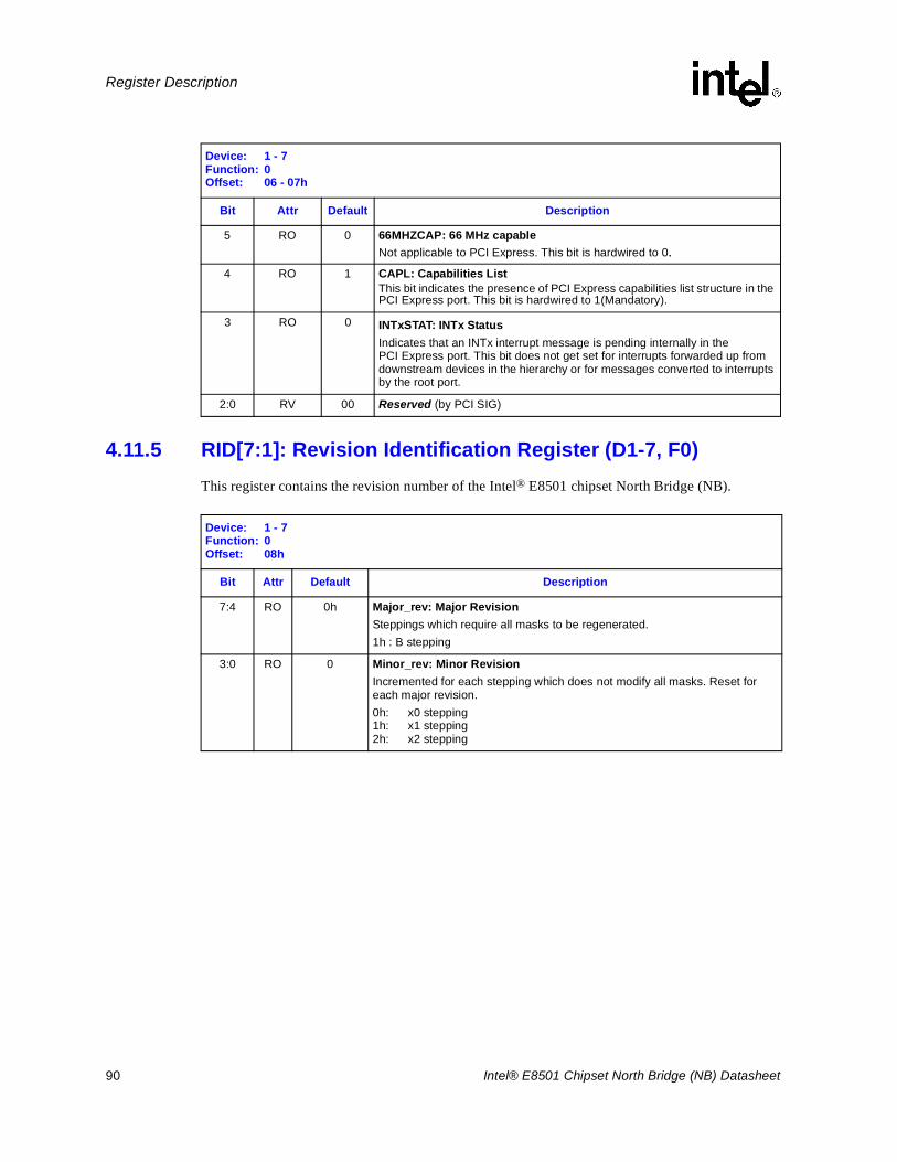
90 Intel® E8501 Chipset North Bridge (NB) Datasheet
Register Description
4.11.5 RID[7:1]: Revision Identification Register (D1-7, F0)This register contains the revision number of the Intel® E8501 chipset North Bridge (NB).
5 RO 0 66MHZCAP: 66 MHz capableNot applicable to PCI Express. This bit is hardwired to 0.
4 RO 1 CAPL: Capabilities ListThis bit indicates the presence of PCI Express capabilities list structure in the PCI Express port. This bit is hardwired to 1(Mandatory).
3 RO 0 INTxSTAT: INTx StatusIndicates that an INTx interrupt message is pending internally in the PCI Express port. This bit does not get set for interrupts forwarded up from downstream devices in the hierarchy or for messages converted to interrupts by the root port.
2:0 RV 00 Reserved (by PCI SIG)
Device: 1 - 7Function: 0Offset: 06 - 07h
Bit Attr Default Description
Device: 1 - 7Function: 0Offset: 08h
Bit Attr Default Description
7:4 RO 0h Major_rev: Major RevisionSteppings which require all masks to be regenerated.1h : B stepping
3:0 RO 0 Minor_rev: Minor RevisionIncremented for each stepping which does not modify all masks. Reset for each major revision.0h: x0 stepping1h: x1 stepping2h: x2 stepping
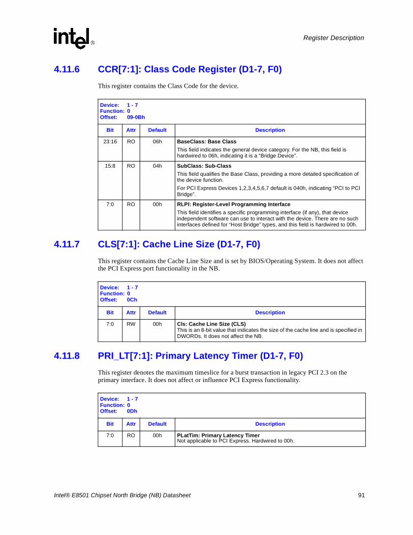
Intel® E8501 Chipset North Bridge (NB) Datasheet 91
Register Description
4.11.6 CCR[7:1]: Class Code Register (D1-7, F0)This register contains the Class Code for the device.
4.11.7 CLS[7:1]: Cache Line Size (D1-7, F0)This register contains the Cache Line Size and is set by BIOS/Operating System. It does not affect the PCI Express port functionality in the NB.
4.11.8 PRI_LT[7:1]: Primary Latency Timer (D1-7, F0)This register denotes the maximum timeslice for a burst transaction in legacy PCI 2.3 on the primary interface. It does not affect or influence PCI Express functionality.
Device: 1 - 7Function: 0Offset: 09-0Bh
Bit Attr Default Description
23:16 RO 06h BaseClass: Base ClassThis field indicates the general device category. For the NB, this field is hardwired to 06h, indicating it is a “Bridge Device”.
15:8 RO 04h SubClass: Sub-ClassThis field qualifies the Base Class, providing a more detailed specification of the device function. For PCI Express Devices 1,2,3,4,5,6,7 default is 040h, indicating “PCI to PCI Bridge”.
7:0 RO 00h RLPI: Register-Level Programming InterfaceThis field identifies a specific programming interface (if any), that device independent software can use to interact with the device. There are no such interfaces defined for “Host Bridge” types, and this field is hardwired to 00h.
Device: 1 - 7Function: 0Offset: 0Ch
Bit Attr Default Description
7:0 RW 00h Cls: Cache Line Size (CLS)This is an 8-bit value that indicates the size of the cache line and is specified in DWORDs. It does not affect the NB.
Device: 1 - 7Function: 0Offset: 0Dh
Bit Attr Default Description
7:0 RO 00h PLatTim: Primary Latency Timer Not applicable to PCI Express. Hardwired to 00h.
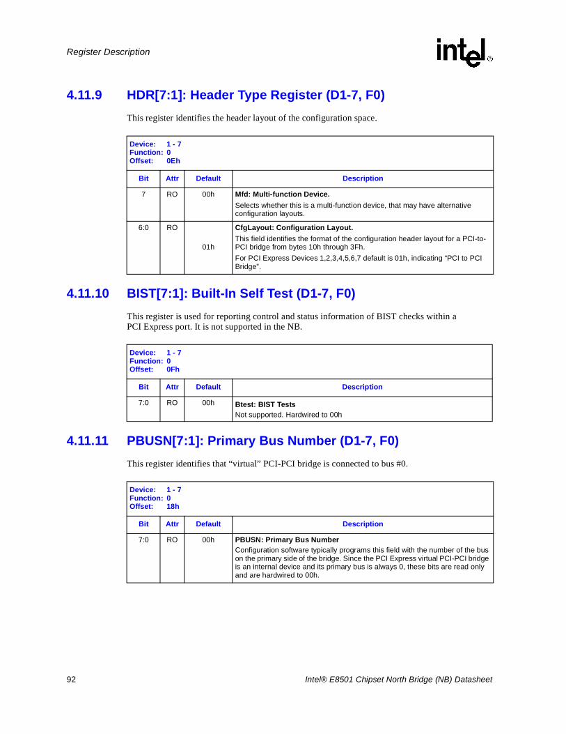
92 Intel® E8501 Chipset North Bridge (NB) Datasheet
Register Description
4.11.9 HDR[7:1]: Header Type Register (D1-7, F0)This register identifies the header layout of the configuration space.
4.11.10 BIST[7:1]: Built-In Self Test (D1-7, F0)This register is used for reporting control and status information of BIST checks within a PCI Express port. It is not supported in the NB.
4.11.11 PBUSN[7:1]: Primary Bus Number (D1-7, F0)This register identifies that “virtual” PCI-PCI bridge is connected to bus #0.
Device: 1 - 7Function: 0Offset: 0Eh
Bit Attr Default Description
7 RO 00h Mfd: Multi-function Device.Selects whether this is a multi-function device, that may have alternative configuration layouts.
6:0 RO
01h
CfgLayout: Configuration Layout.This field identifies the format of the configuration header layout for a PCI-to-PCI bridge from bytes 10h through 3Fh. For PCI Express Devices 1,2,3,4,5,6,7 default is 01h, indicating “PCI to PCI Bridge”.
Device: 1 - 7Function: 0Offset: 0Fh
Bit Attr Default Description
7:0 RO 00h Btest: BIST TestsNot supported. Hardwired to 00h
Device: 1 - 7Function: 0Offset: 18h
Bit Attr Default Description
7:0 RO 00h PBUSN: Primary Bus Number Configuration software typically programs this field with the number of the bus on the primary side of the bridge. Since the PCI Express virtual PCI-PCI bridge is an internal device and its primary bus is always 0, these bits are read only and are hardwired to 00h.
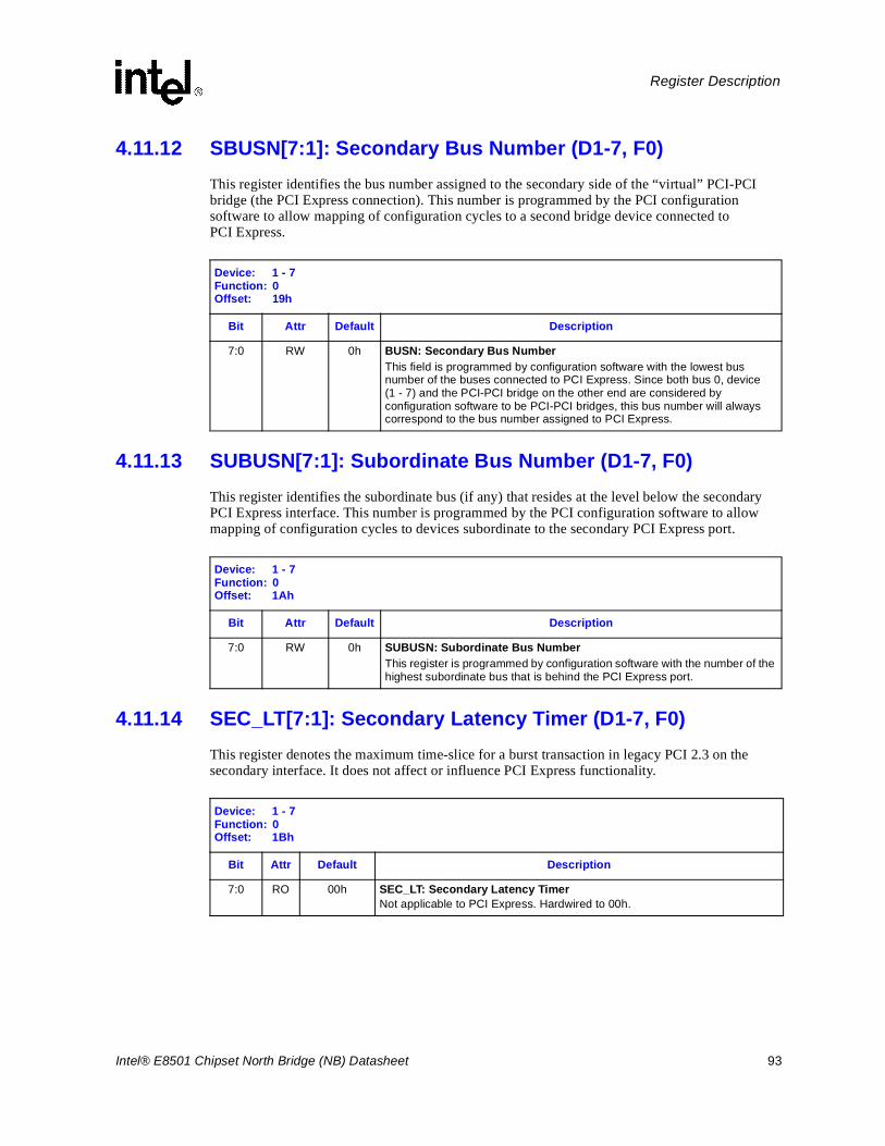
Intel® E8501 Chipset North Bridge (NB) Datasheet 93
Register Description
4.11.12 SBUSN[7:1]: Secondary Bus Number (D1-7, F0)This register identifies the bus number assigned to the secondary side of the “virtual” PCI-PCI bridge (the PCI Express connection). This number is programmed by the PCI configuration software to allow mapping of configuration cycles to a second bridge device connected to PCI Express.
4.11.13 SUBUSN[7:1]: Subordinate Bus Number (D1-7, F0)This register identifies the subordinate bus (if any) that resides at the level below the secondary PCI Express interface. This number is programmed by the PCI configuration software to allow mapping of configuration cycles to devices subordinate to the secondary PCI Express port.
4.11.14 SEC_LT[7:1]: Secondary Latency Timer (D1-7, F0)This register denotes the maximum time-slice for a burst transaction in legacy PCI 2.3 on the secondary interface. It does not affect or influence PCI Express functionality.
Device: 1 - 7Function: 0Offset: 19h
Bit Attr Default Description
7:0 RW 0h BUSN: Secondary Bus NumberThis field is programmed by configuration software with the lowest bus number of the buses connected to PCI Express. Since both bus 0, device (1 - 7) and the PCI-PCI bridge on the other end are considered by configuration software to be PCI-PCI bridges, this bus number will always correspond to the bus number assigned to PCI Express.
Device: 1 - 7Function: 0Offset: 1Ah
Bit Attr Default Description
7:0 RW 0h SUBUSN: Subordinate Bus Number This register is programmed by configuration software with the number of the highest subordinate bus that is behind the PCI Express port.
Device: 1 - 7Function: 0Offset: 1Bh
Bit Attr Default Description
7:0 RO 00h SEC_LT: Secondary Latency TimerNot applicable to PCI Express. Hardwired to 00h.
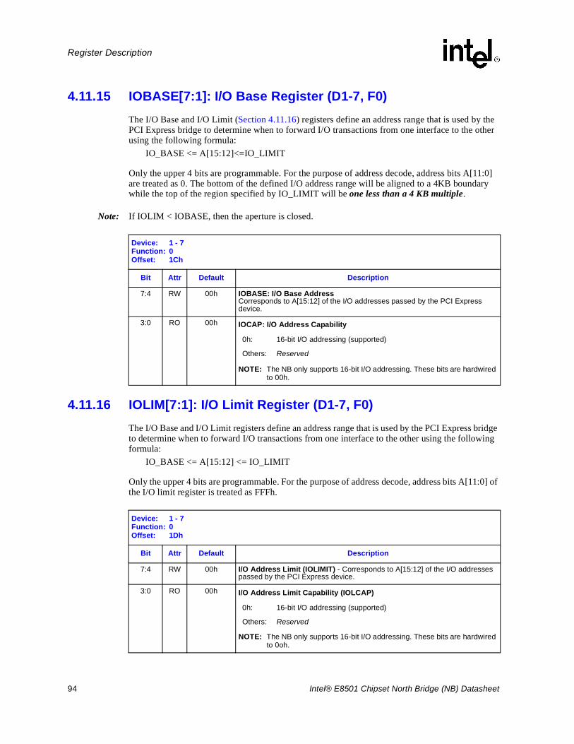
94 Intel® E8501 Chipset North Bridge (NB) Datasheet
Register Description
4.11.15 IOBASE[7:1]: I/O Base Register (D1-7, F0)The I/O Base and I/O Limit (Section 4.11.16) registers define an address range that is used by the PCI Express bridge to determine when to forward I/O transactions from one interface to the other using the following formula:
IO_BASE <= A[15:12]<=IO_LIMIT
Only the upper 4 bits are programmable. For the purpose of address decode, address bits A[11:0] are treated as 0. The bottom of the defined I/O address range will be aligned to a 4KB boundary while the top of the region specified by IO_LIMIT will be one less than a 4 KB multiple.
Note: If IOLIM < IOBASE, then the aperture is closed.
4.11.16 IOLIM[7:1]: I/O Limit Register (D1-7, F0)The I/O Base and I/O Limit registers define an address range that is used by the PCI Express bridge to determine when to forward I/O transactions from one interface to the other using the following formula:
IO_BASE <= A[15:12] <= IO_LIMIT
Only the upper 4 bits are programmable. For the purpose of address decode, address bits A[11:0] of the I/O limit register is treated as FFFh.
Device: 1 - 7Function: 0Offset: 1Ch
Bit Attr Default Description
7:4 RW 00h IOBASE: I/O Base Address Corresponds to A[15:12] of the I/O addresses passed by the PCI Express device.
3:0 RO 00h IOCAP: I/O Address Capability
NOTE: The NB only supports 16-bit I/O addressing. These bits are hardwired to 00h.
0h: 16-bit I/O addressing (supported)
Others: Reserved
Device: 1 - 7Function: 0Offset: 1Dh
Bit Attr Default Description
7:4 RW 00h I/O Address Limit (IOLIMIT) - Corresponds to A[15:12] of the I/O addresses passed by the PCI Express device.
3:0 RO 00h I/O Address Limit Capability (IOLCAP)
NOTE: The NB only supports 16-bit I/O addressing. These bits are hardwired to 0oh.
0h: 16-bit I/O addressing (supported)
Others: Reserved
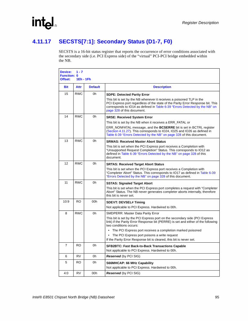
Intel® E8501 Chipset North Bridge (NB) Datasheet 95
Register Description
4.11.17 SECSTS[7:1]: Secondary Status (D1-7, F0)SECSTS is a 16-bit status register that reports the occurrence of error conditions associated with the secondary side (i.e. PCI Express side) of the “virtual” PCI-PCI bridge embedded within the NB.
Device: 1 - 7Function: 0Offset: 1Eh - 1Fh
Bit Attr Default Description
15 RWC 0h SDPE: Detected Parity ErrorThis bit is set by the NB whenever it receives a poisoned TLP in the PCI Express port regardless of the state of the Parity Error Response bit. This corresponds to IO14 as defined in Table 6-39 “Errors Detected by the NB” on page 328 of this document.
14 RWC 0h SRSE: Received System ErrorThis bit is set by the NB when it receives a ERR_FATAL orERR_NONFATAL message, and the BCSERRE bit is set in BCTRL register (Section 4.11.27). This corresponds to IO24, IO25 and IO26 as defined in Table 6-39 “Errors Detected by the NB” on page 328 of this document.
13 RWC 0h SRMAS: Received Master Abort StatusThis bit is set when the PCI Express port receives a Completion with “Unsupported Request Completion” Status. This corresponds to IO12 as defined in Table 6-39 “Errors Detected by the NB” on page 328 of this document.
12 RWC 0h SRTAS: Received Target Abort StatusThis bit is set when the PCI Express port receives a Completion with “Completer Abort” Status. This corresponds to IO17 as defined in Table 6-39 “Errors Detected by the NB” on page 328 of this document.
11 RWC 0h SSTAS: Signaled Target AbortThis bit is set when the PCI Express port completes a request with “Completer Abort” Status. The NB never generates completer aborts internally, therefore this bit is never set.
10:9 RO 00h SDEVT: DEVSEL# TimingNot applicable to PCI Express. Hardwired to 00h.
8 RWC 0h SMDPERR: Master Data Parity ErrorThis bit is set by the PCI Express port on the secondary side (PCI Express link) if the Parity Error Response bit (PERRE) is set and either of the following two conditions occurs:
• The PCI Express port receives a completion marked poisoned• The PCI Express port poisons a write request
If the Parity Error Response bit is cleared, this bit is never set.
7 RO 0h SFB2BTC: Fast Back-to-Back Transactions CapableNot applicable to PCI Express. Hardwired to 00h.
6 RV 0h Reserved (by PCI SIG)
5 RO 0h S66MHCAP: 66 MHz CapabilityNot applicable to PCI Express. Hardwired to 00h.
4:0 RV 00h Reserved (by PCI SIG)
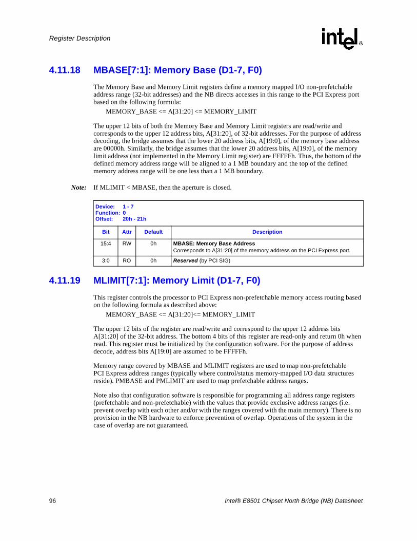
96 Intel® E8501 Chipset North Bridge (NB) Datasheet
Register Description
4.11.18 MBASE[7:1]: Memory Base (D1-7, F0)The Memory Base and Memory Limit registers define a memory mapped I/O non-prefetchable address range (32-bit addresses) and the NB directs accesses in this range to the PCI Express port based on the following formula:
MEMORY_BASE <= A[31:20] <= MEMORY_LIMIT
The upper 12 bits of both the Memory Base and Memory Limit registers are read/write and corresponds to the upper 12 address bits, A[31:20], of 32-bit addresses. For the purpose of address decoding, the bridge assumes that the lower 20 address bits, A[19:0], of the memory base address are 00000h. Similarly, the bridge assumes that the lower 20 address bits, A[19:0], of the memory limit address (not implemented in the Memory Limit register) are FFFFFh. Thus, the bottom of the defined memory address range will be aligned to a 1 MB boundary and the top of the defined memory address range will be one less than a 1 MB boundary.
Note: If MLIMIT < MBASE, then the aperture is closed.
4.11.19 MLIMIT[7:1]: Memory Limit (D1-7, F0)This register controls the processor to PCI Express non-prefetchable memory access routing based on the following formula as described above:
MEMORY_BASE <= A[31:20]<= MEMORY_LIMIT
The upper 12 bits of the register are read/write and correspond to the upper 12 address bits A[31:20] of the 32-bit address. The bottom 4 bits of this register are read-only and return 0h when read. This register must be initialized by the configuration software. For the purpose of address decode, address bits A[19:0] are assumed to be FFFFFh.
Memory range covered by MBASE and MLIMIT registers are used to map non-prefetchable PCI Express address ranges (typically where control/status memory-mapped I/O data structures reside). PMBASE and PMLIMIT are used to map prefetchable address ranges.
Note also that configuration software is responsible for programming all address range registers (prefetchable and non-prefetchable) with the values that provide exclusive address ranges (i.e. prevent overlap with each other and/or with the ranges covered with the main memory). There is no provision in the NB hardware to enforce prevention of overlap. Operations of the system in the case of overlap are not guaranteed.
Device: 1 - 7Function: 0Offset: 20h - 21h
Bit Attr Default Description
15:4 RW 0h MBASE: Memory Base AddressCorresponds to A[31:20] of the memory address on the PCI Express port.
3:0 RO 0h Reserved (by PCI SIG)
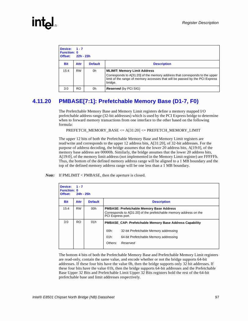
Intel® E8501 Chipset North Bridge (NB) Datasheet 97
Register Description
4.11.20 PMBASE[7:1]: Prefetchable Memory Base (D1-7, F0)The Prefetchable Memory Base and Memory Limit registers define a memory mapped I/O prefetchable address range (32-bit addresses) which is used by the PCI Express bridge to determine when to forward memory transactions from one interface to the other based on the following formula:
PREFETCH_MEMORY_BASE <= A[31:20] <= PREFETCH_MEMORY_LIMIT
The upper 12 bits of both the Prefetchable Memory Base and Memory Limit registers are read/write and corresponds to the upper 12 address bits, A[31:20], of 32-bit addresses. For the purpose of address decoding, the bridge assumes that the lower 20 address bits, A[19:0], of the memory base address are 00000h. Similarly, the bridge assumes that the lower 20 address bits, A[19:0], of the memory limit address (not implemented in the Memory Limit register) are FFFFFh. Thus, the bottom of the defined memory address range will be aligned to a 1 MB boundary and the top of the defined memory address range will be one less than a 1 MB boundary.
Note: If PMLIMIT < PMBASE, then the aperture is closed.
The bottom 4 bits of both the Prefetchable Memory Base and Prefetchable Memory Limit registers are read-only, contain the same value, and encode whether or not the bridge supports 64-bit addresses. If these four bits have the value 0h, then the bridge supports only 32 bit addresses. If these four bits have the value 01h, then the bridge supports 64-bit addresses and the Prefetchable Base Upper 32 Bits and Prefetchable Limit Upper 32 Bits registers hold the rest of the 64-bit prefetchable base and limit addresses respectively.
Device: 1 - 7Function: 0Offset: 22h - 23h
Bit Attr Default Description
15:4 RW 0h MLIMIT: Memory Limit AddressCorresponds to A[31:20] of the memory address that corresponds to the upper limit of the range of memory accesses that will be passed by the PCI Express bridge.
3:0 RO 0h Reserved (by PCI SIG)
Device: 1 - 7Function: 0Offset: 24h - 25h
Bit Attr Default Description
15:4 RW 00h PMBASE: Prefetchable Memory Base Address Corresponds to A[31:20] of the prefetchable memory address on the PCI Express port.
3:0 RO 01h PMBASE_CAP: Prefetchable Memory Base Address Capability
00h: 32-bit Prefetchable Memory addressing
01h: 64-bit Prefetchable Memory addressing
Others: Reserved
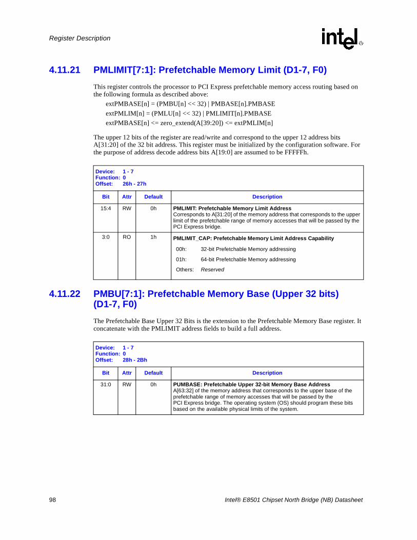
98 Intel® E8501 Chipset North Bridge (NB) Datasheet
Register Description
4.11.21 PMLIMIT[7:1]: Prefetchable Memory Limit (D1-7, F0)This register controls the processor to PCI Express prefetchable memory access routing based on the following formula as described above:
extPMBASE[n] = (PMBU[n] << 32) | PMBASE[n].PMBASEextPMLIM[n] = (PMLU[n] << 32) | PMLIMIT[n].PMBASEextPMBASE[n] <= zero_extend(A[39:20]) <= extPMLIM[n]
The upper 12 bits of the register are read/write and correspond to the upper 12 address bits A[31:20] of the 32 bit address. This register must be initialized by the configuration software. For the purpose of address decode address bits A[19:0] are assumed to be FFFFFh.
4.11.22 PMBU[7:1]: Prefetchable Memory Base (Upper 32 bits) (D1-7, F0)The Prefetchable Base Upper 32 Bits is the extension to the Prefetchable Memory Base register. It concatenate with the PMLIMIT address fields to build a full address.
Device: 1 - 7Function: 0Offset: 26h - 27h
Bit Attr Default Description
15:4 RW 0h PMLIMIT: Prefetchable Memory Limit Address Corresponds to A[31:20] of the memory address that corresponds to the upper limit of the prefetchable range of memory accesses that will be passed by the PCI Express bridge.
3:0 RO 1h PMLIMIT_CAP: Prefetchable Memory Limit Address Capability
00h: 32-bit Prefetchable Memory addressing
01h: 64-bit Prefetchable Memory addressing
Others: Reserved
Device: 1 - 7Function: 0Offset: 28h - 2Bh
Bit Attr Default Description
31:0 RW 0h PUMBASE: Prefetchable Upper 32-bit Memory Base AddressA[63:32] of the memory address that corresponds to the upper base of the prefetchable range of memory accesses that will be passed by the PCI Express bridge. The operating system (OS) should program these bits based on the available physical limits of the system.
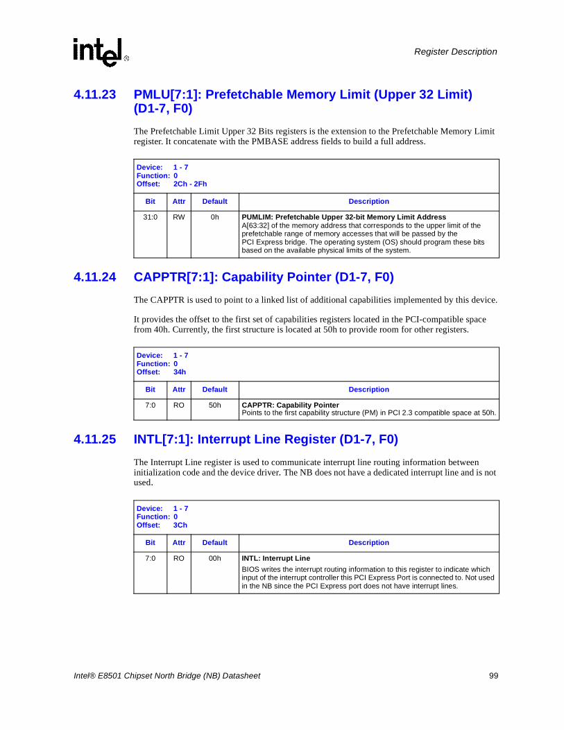
Intel® E8501 Chipset North Bridge (NB) Datasheet 99
Register Description
4.11.23 PMLU[7:1]: Prefetchable Memory Limit (Upper 32 Limit) (D1-7, F0)The Prefetchable Limit Upper 32 Bits registers is the extension to the Prefetchable Memory Limit register. It concatenate with the PMBASE address fields to build a full address.
4.11.24 CAPPTR[7:1]: Capability Pointer (D1-7, F0)The CAPPTR is used to point to a linked list of additional capabilities implemented by this device.
It provides the offset to the first set of capabilities registers located in the PCI-compatible space from 40h. Currently, the first structure is located at 50h to provide room for other registers.
4.11.25 INTL[7:1]: Interrupt Line Register (D1-7, F0)The Interrupt Line register is used to communicate interrupt line routing information between initialization code and the device driver. The NB does not have a dedicated interrupt line and is not used.
Device: 1 - 7Function: 0Offset: 2Ch - 2Fh
Bit Attr Default Description
31:0 RW 0h PUMLIM: Prefetchable Upper 32-bit Memory Limit Address A[63:32] of the memory address that corresponds to the upper limit of the prefetchable range of memory accesses that will be passed by the PCI Express bridge. The operating system (OS) should program these bits based on the available physical limits of the system.
Device: 1 - 7Function: 0Offset: 34h
Bit Attr Default Description
7:0 RO 50h CAPPTR: Capability Pointer Points to the first capability structure (PM) in PCI 2.3 compatible space at 50h.
Device: 1 - 7Function: 0Offset: 3Ch
Bit Attr Default Description
7:0 RO 00h INTL: Interrupt LineBIOS writes the interrupt routing information to this register to indicate which input of the interrupt controller this PCI Express Port is connected to. Not used in the NB since the PCI Express port does not have interrupt lines.
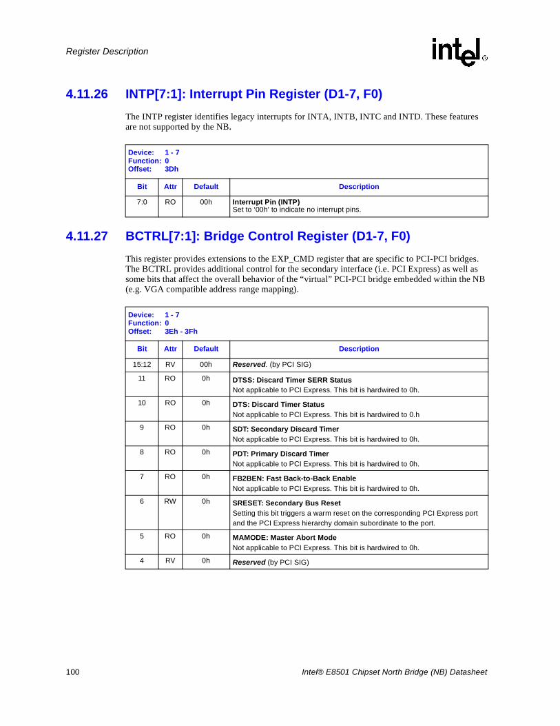
100 Intel® E8501 Chipset North Bridge (NB) Datasheet
Register Description
4.11.26 INTP[7:1]: Interrupt Pin Register (D1-7, F0)The INTP register identifies legacy interrupts for INTA, INTB, INTC and INTD. These features are not supported by the NB.
4.11.27 BCTRL[7:1]: Bridge Control Register (D1-7, F0)This register provides extensions to the EXP_CMD register that are specific to PCI-PCI bridges. The BCTRL provides additional control for the secondary interface (i.e. PCI Express) as well as some bits that affect the overall behavior of the “virtual” PCI-PCI bridge embedded within the NB (e.g. VGA compatible address range mapping).
Device: 1 - 7Function: 0Offset: 3Dh
Bit Attr Default Description
7:0 RO 00h Interrupt Pin (INTP)Set to ‘00h’ to indicate no interrupt pins.
Device: 1 - 7Function: 0Offset: 3Eh - 3Fh
Bit Attr Default Description
15:12 RV 00h Reserved. (by PCI SIG)
11 RO 0h DTSS: Discard Timer SERR StatusNot applicable to PCI Express. This bit is hardwired to 0h.
10 RO 0h DTS: Discard Timer StatusNot applicable to PCI Express. This bit is hardwired to 0.h
9 RO 0h SDT: Secondary Discard TimerNot applicable to PCI Express. This bit is hardwired to 0h.
8 RO 0h PDT: Primary Discard TimerNot applicable to PCI Express. This bit is hardwired to 0h.
7 RO 0h FB2BEN: Fast Back-to-Back EnableNot applicable to PCI Express. This bit is hardwired to 0h.
6 RW 0h SRESET: Secondary Bus ResetSetting this bit triggers a warm reset on the corresponding PCI Express port and the PCI Express hierarchy domain subordinate to the port.
5 RO 0h MAMODE: Master Abort ModeNot applicable to PCI Express. This bit is hardwired to 0h.
4 RV 0h Reserved (by PCI SIG)
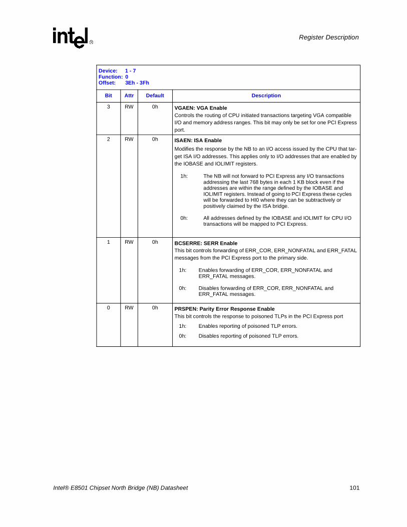
Intel® E8501 Chipset North Bridge (NB) Datasheet 101
Register Description
3 RW 0h VGAEN: VGA EnableControls the routing of CPU initiated transactions targeting VGA compatible I/O and memory address ranges. This bit may only be set for one PCI Express port.
2 RW 0h ISAEN: ISA EnableModifies the response by the NB to an I/O access issued by the CPU that tar-get ISA I/O addresses. This applies only to I/O addresses that are enabled by the IOBASE and IOLIMIT registers.
1 RW 0h BCSERRE: SERR EnableThis bit controls forwarding of ERR_COR, ERR_NONFATAL and ERR_FATAL messages from the PCI Express port to the primary side.
0 RW 0h PRSPEN: Parity Error Response EnableThis bit controls the response to poisoned TLPs in the PCI Express port
Device: 1 - 7Function: 0Offset: 3Eh - 3Fh
Bit Attr Default Description
1h: The NB will not forward to PCI Express any I/O transactions addressing the last 768 bytes in each 1 KB block even if the addresses are within the range defined by the IOBASE and IOLIMIT registers. Instead of going to PCI Express these cycles will be forwarded to HI0 where they can be subtractively or positively claimed by the ISA bridge.
0h: All addresses defined by the IOBASE and IOLIMIT for CPU I/O transactions will be mapped to PCI Express.
1h: Enables forwarding of ERR_COR, ERR_NONFATAL and ERR_FATAL messages.
0h: Disables forwarding of ERR_COR, ERR_NONFATAL and ERR_FATAL messages.
1h: Enables reporting of poisoned TLP errors.
0h: Disables reporting of poisoned TLP errors.
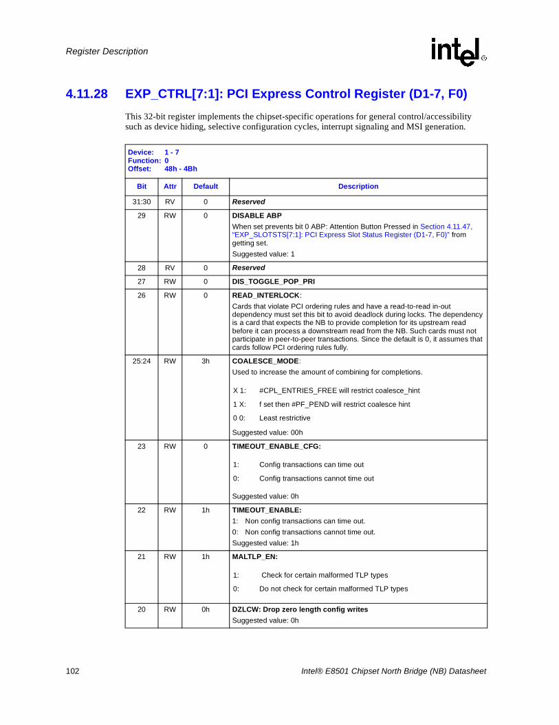
102 Intel® E8501 Chipset North Bridge (NB) Datasheet
Register Description
4.11.28 EXP_CTRL[7:1]: PCI Express Control Register (D1-7, F0)This 32-bit register implements the chipset-specific operations for general control/accessibility such as device hiding, selective configuration cycles, interrupt signaling and MSI generation.
Device: 1 - 7Function: 0Offset: 48h - 4Bh
Bit Attr Default Description
31:30 RV 0 Reserved
29 RW 0 DISABLE ABPWhen set prevents bit 0 ABP: Attention Button Pressed in Section 4.11.47, “EXP_SLOTSTS[7:1]: PCI Express Slot Status Register (D1-7, F0)” fromgetting set.Suggested value: 1
28 RV 0 Reserved
27 RW 0 DIS_TOGGLE_POP_PRI
26 RW 0 READ_INTERLOCK:Cards that violate PCI ordering rules and have a read-to-read in-out dependency must set this bit to avoid deadlock during locks. The dependency is a card that expects the NB to provide completion for its upstream read before it can process a downstream read from the NB. Such cards must not participate in peer-to-peer transactions. Since the default is 0, it assumes that cards follow PCI ordering rules fully.
25:24 RW 3h COALESCE_MODE:Used to increase the amount of combining for completions.
Suggested value: 00h
23 RW 0 TIMEOUT_ENABLE_CFG:
Suggested value: 0h
22 RW 1h TIMEOUT_ENABLE: 1: Non config transactions can time out.0: Non config transactions cannot time out.Suggested value: 1h
21 RW 1h MALTLP_EN:
20 RW 0h DZLCW: Drop zero length config writesSuggested value: 0h
X 1: #CPL_ENTRIES_FREE will restrict coalesce_hint
1 X: f set then #PF_PEND will restrict coalesce hint
0 0: Least restrictive
1: Config transactions can time out
0: Config transactions cannot time out
1: Check for certain malformed TLP types
0: Do not check for certain malformed TLP types
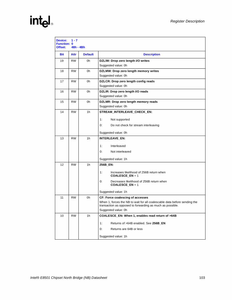
Intel® E8501 Chipset North Bridge (NB) Datasheet 103
Register Description
19 RW 0h DZLIW: Drop zero length I/O writesSuggested value: 0h
18 RW 0h DZLMW: Drop zero length memory writesSuggested value: 0h
17 RW 0h DZLCR: Drop zero length config readsSuggested value: 0h
16 RW 0h DZLIR: Drop zero length I/O readsSuggested value: 0h
15 RW 0h DZLMR: Drop zero length memory readsSuggested value: 0h
14 RW 1h STREAM_INTERLEAVE_CHECK_EN:
Suggested value: 0h
13 RW 1h INTERLEAVE_EN:
Suggested value: 1h
12 RW 1h 256B_EN:
Suggested value: 1h
11 RW 0h CF: Force coalescing of accessesWhen 1, forces the NB to wait for all coalescable data before sending the transaction as opposed to forwarding as much as possible.Suggested value: 0h
10 RW 1h COALESCE_EN: When 1, enables read return of >64B
Suggested value: 1h
Device: 1 - 7Function: 0Offset: 48h - 4Bh
Bit Attr Default Description
1: Not supported
0: Do not check for stream interleaving
1: Interleaved
0: Not interleaved
1: Increases likelihood of 256B return when COALESCE_EN = 1
0: Decreases likelihood of 256B return when COALESCE_EN = 1
1: Returns of >64B enabled. See 256B_EN
0: Returns are 64B or less
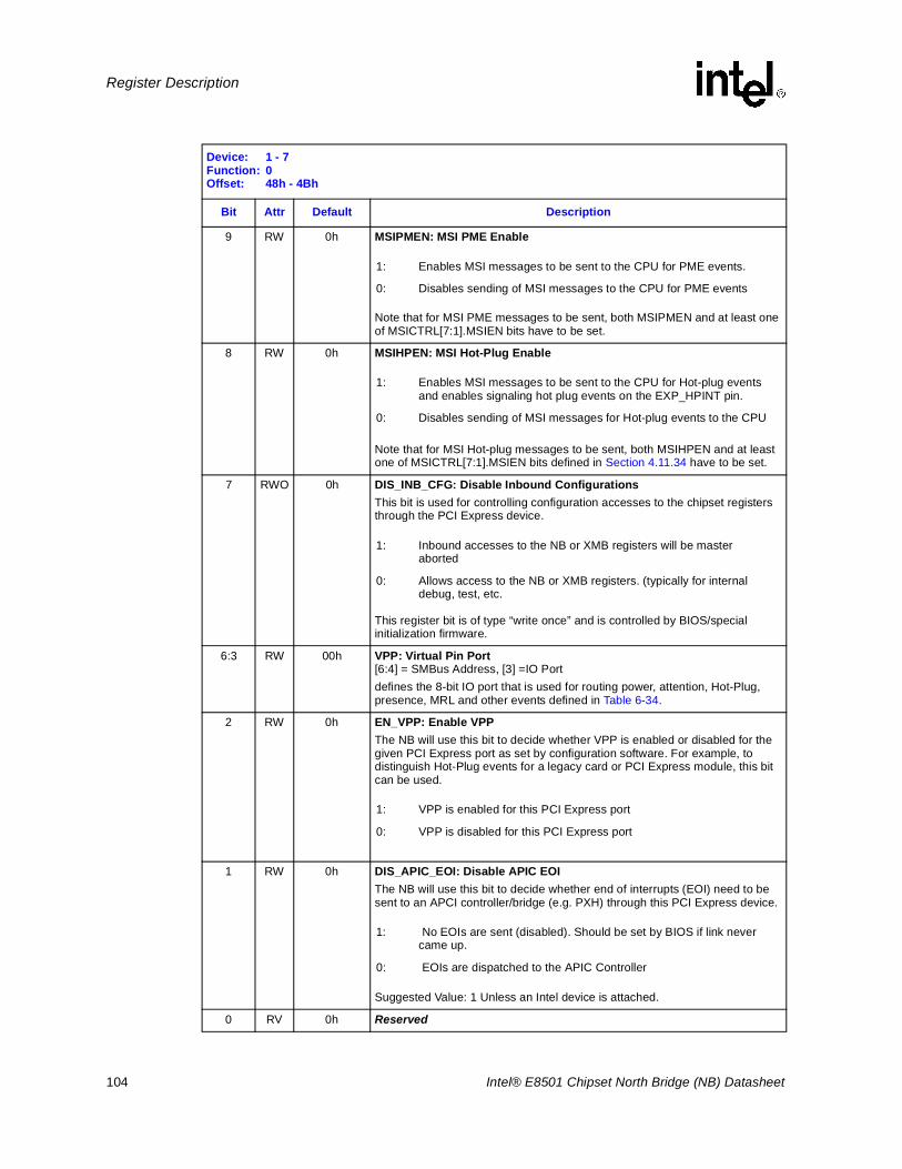
104 Intel® E8501 Chipset North Bridge (NB) Datasheet
Register Description
9 RW 0h MSIPMEN: MSI PME Enable
Note that for MSI PME messages to be sent, both MSIPMEN and at least one of MSICTRL[7:1].MSIEN bits have to be set.
8 RW 0h MSIHPEN: MSI Hot-Plug Enable
Note that for MSI Hot-plug messages to be sent, both MSIHPEN and at least one of MSICTRL[7:1].MSIEN bits defined in Section 4.11.34 have to be set.
7 RWO 0h DIS_INB_CFG: Disable Inbound ConfigurationsThis bit is used for controlling configuration accesses to the chipset registers through the PCI Express device.
This register bit is of type “write once” and is controlled by BIOS/special initialization firmware.
6:3 RW 00h VPP: Virtual Pin Port [6:4] = SMBus Address, [3] =IO Portdefines the 8-bit IO port that is used for routing power, attention, Hot-Plug, presence, MRL and other events defined in Table 6-34.
2 RW 0h EN_VPP: Enable VPPThe NB will use this bit to decide whether VPP is enabled or disabled for the given PCI Express port as set by configuration software. For example, to distinguish Hot-Plug events for a legacy card or PCI Express module, this bit can be used.
1 RW 0h DIS_APIC_EOI: Disable APIC EOIThe NB will use this bit to decide whether end of interrupts (EOI) need to be sent to an APCI controller/bridge (e.g. PXH) through this PCI Express device.
Suggested Value: 1 Unless an Intel device is attached.
0 RV 0h Reserved
Device: 1 - 7Function: 0Offset: 48h - 4Bh
Bit Attr Default Description
1: Enables MSI messages to be sent to the CPU for PME events.
0: Disables sending of MSI messages to the CPU for PME events
1: Enables MSI messages to be sent to the CPU for Hot-plug events and enables signaling hot plug events on the EXP_HPINT pin.
0: Disables sending of MSI messages for Hot-plug events to the CPU
1: Inbound accesses to the NB or XMB registers will be master aborted
0: Allows access to the NB or XMB registers. (typically for internal debug, test, etc.
1: VPP is enabled for this PCI Express port
0: VPP is disabled for this PCI Express port
1: No EOIs are sent (disabled). Should be set by BIOS if link never came up.
0: EOIs are dispatched to the APIC Controller
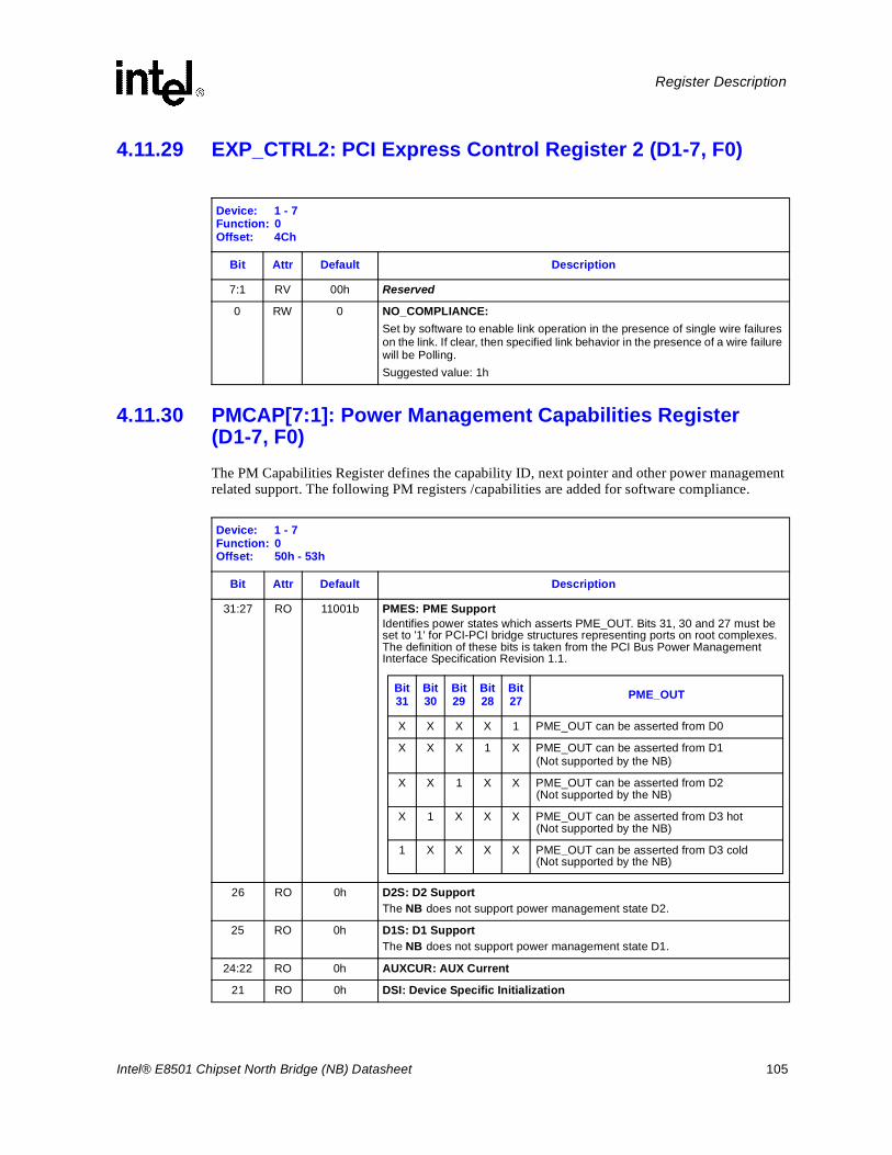
Intel® E8501 Chipset North Bridge (NB) Datasheet 105
Register Description
4.11.29 EXP_CTRL2: PCI Express Control Register 2 (D1-7, F0)
4.11.30 PMCAP[7:1]: Power Management Capabilities Register (D1-7, F0)The PM Capabilities Register defines the capability ID, next pointer and other power management related support. The following PM registers /capabilities are added for software compliance.
Device: 1 - 7Function: 0Offset: 4Ch
Bit Attr Default Description
7:1 RV 00h Reserved
0 RW 0 NO_COMPLIANCE: Set by software to enable link operation in the presence of single wire failures on the link. If clear, then specified link behavior in the presence of a wire failure will be Polling.Suggested value: 1h
Device: 1 - 7Function: 0Offset: 50h - 53h
Bit Attr Default Description
31:27 RO 11001b PMES: PME Support Identifies power states which asserts PME_OUT. Bits 31, 30 and 27 must be set to '1' for PCI-PCI bridge structures representing ports on root complexes. The definition of these bits is taken from the PCI Bus Power Management Interface Specification Revision 1.1.
26 RO 0h D2S: D2 SupportThe NB does not support power management state D2.
25 RO 0h D1S: D1 SupportThe NB does not support power management state D1.
24:22 RO 0h AUXCUR: AUX Current
21 RO 0h DSI: Device Specific Initialization
Bit 31
Bit 30
Bit 29
Bit 28
Bit 27 PME_OUT
X X X X 1 PME_OUT can be asserted from D0
X X X 1 X PME_OUT can be asserted from D1 (Not supported by the NB)
X X 1 X X PME_OUT can be asserted from D2 (Not supported by the NB)
X 1 X X X PME_OUT can be asserted from D3 hot (Not supported by the NB)
1 X X X X PME_OUT can be asserted from D3 cold(Not supported by the NB)
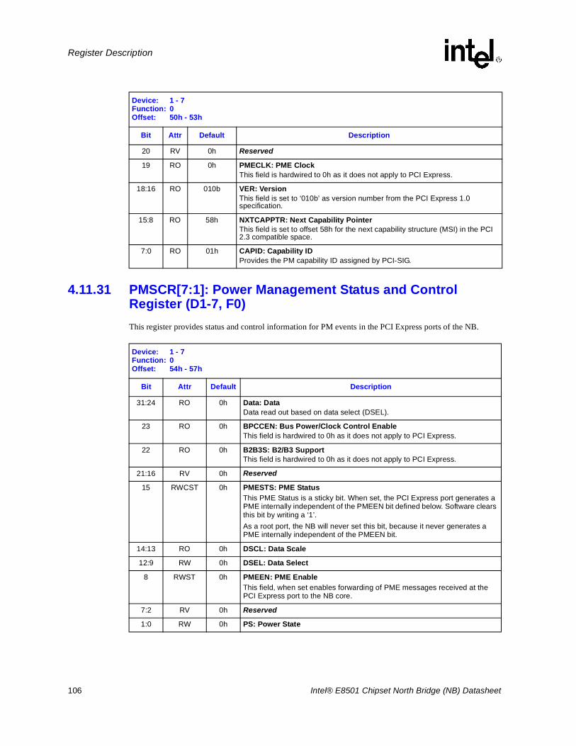
106 Intel® E8501 Chipset North Bridge (NB) Datasheet
Register Description
4.11.31 PMSCR[7:1]: Power Management Status and Control Register (D1-7, F0)This register provides status and control information for PM events in the PCI Express ports of the NB.
20 RV 0h Reserved
19 RO 0h PMECLK: PME ClockThis field is hardwired to 0h as it does not apply to PCI Express.
18:16 RO 010b VER: VersionThis field is set to ‘010b’ as version number from the PCI Express 1.0 specification.
15:8 RO 58h NXTCAPPTR: Next Capability PointerThis field is set to offset 58h for the next capability structure (MSI) in the PCI 2.3 compatible space.
7:0 RO 01h CAPID: Capability IDProvides the PM capability ID assigned by PCI-SIG.
Device: 1 - 7Function: 0Offset: 50h - 53h
Bit Attr Default Description
Device: 1 - 7Function: 0Offset: 54h - 57h
Bit Attr Default Description
31:24 RO 0h Data: DataData read out based on data select (DSEL).
23 RO 0h BPCCEN: Bus Power/Clock Control EnableThis field is hardwired to 0h as it does not apply to PCI Express.
22 RO 0h B2B3S: B2/B3 SupportThis field is hardwired to 0h as it does not apply to PCI Express.
21:16 RV 0h Reserved
15 RWCST 0h PMESTS: PME StatusThis PME Status is a sticky bit. When set, the PCI Express port generates a PME internally independent of the PMEEN bit defined below. Software clears this bit by writing a ‘1’.As a root port, the NB will never set this bit, because it never generates a PME internally independent of the PMEEN bit.
14:13 RO 0h DSCL: Data Scale
12:9 RW 0h DSEL: Data Select
8 RWST 0h PMEEN: PME EnableThis field, when set enables forwarding of PME messages received at the PCI Express port to the NB core.
7:2 RV 0h Reserved
1:0 RW 0h PS: Power State
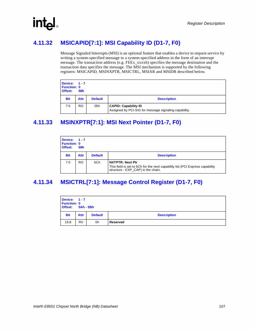
Intel® E8501 Chipset North Bridge (NB) Datasheet 107
Register Description
4.11.32 MSICAPID[7:1]: MSI Capability ID (D1-7, F0)Message Signaled Interrupts (MSI) is an optional feature that enables a device to request service by writing a system-specified message to a system-specified address in the form of an interrupt message. The transaction address (e.g. FEEx_xxxxh) specifies the message destination and the transaction data specifies the message. The MSI mechanism is supported by the following registers: MSICAPID, MSINXPTR, MSICTRL, MSIAR and MSIDR described below.
4.11.33 MSINXPTR[7:1]: MSI Next Pointer (D1-7, F0)
4.11.34 MSICTRL[7:1]: Message Control Register (D1-7, F0)
Device: 1 - 7Function: 0Offset: 58h
Bit Attr Default Description
7:0 RO 05h CAPID: Capability IDAssigned by PCI-SIG for message signaling capability.
Device: 1 - 7Function: 0Offset: 59h
Bit Attr Default Description
7:0 RO 6Ch NXTPTR: Next PtrThis field is set to 6Ch for the next capability list (PCI Express capability structure - EXP_CAP) in the chain.
Device: 1 - 7Function: 0Offset: 5Ah - 5Bh
Bit Attr Default Description
15:8 RV 0h Reserved
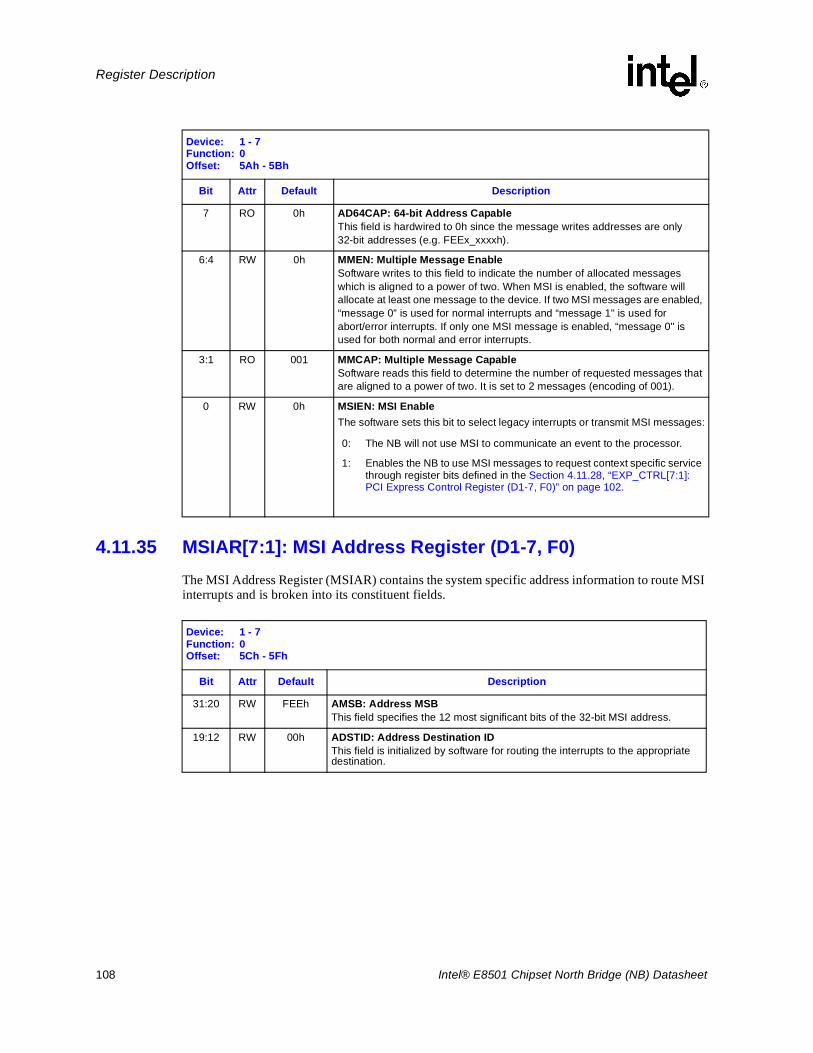
108 Intel® E8501 Chipset North Bridge (NB) Datasheet
Register Description
4.11.35 MSIAR[7:1]: MSI Address Register (D1-7, F0)The MSI Address Register (MSIAR) contains the system specific address information to route MSI interrupts and is broken into its constituent fields.
7 RO 0h AD64CAP: 64-bit Address CapableThis field is hardwired to 0h since the message writes addresses are only 32-bit addresses (e.g. FEEx_xxxxh).
6:4 RW 0h MMEN: Multiple Message EnableSoftware writes to this field to indicate the number of allocated messages which is aligned to a power of two. When MSI is enabled, the software will allocate at least one message to the device. If two MSI messages are enabled, “message 0” is used for normal interrupts and “message 1" is used for abort/error interrupts. If only one MSI message is enabled, “message 0" is used for both normal and error interrupts.
3:1 RO 001 MMCAP: Multiple Message CapableSoftware reads this field to determine the number of requested messages that are aligned to a power of two. It is set to 2 messages (encoding of 001).
0 RW 0h MSIEN: MSI EnableThe software sets this bit to select legacy interrupts or transmit MSI messages:
Device: 1 - 7Function: 0Offset: 5Ah - 5Bh
Bit Attr Default Description
0: The NB will not use MSI to communicate an event to the processor.
1: Enables the NB to use MSI messages to request context specific service through register bits defined in the Section 4.11.28, “EXP_CTRL[7:1]: PCI Express Control Register (D1-7, F0)” on page 102.
Device: 1 - 7Function: 0Offset: 5Ch - 5Fh
Bit Attr Default Description
31:20 RW FEEh AMSB: Address MSBThis field specifies the 12 most significant bits of the 32-bit MSI address.
19:12 RW 00h ADSTID: Address Destination IDThis field is initialized by software for routing the interrupts to the appropriate destination.
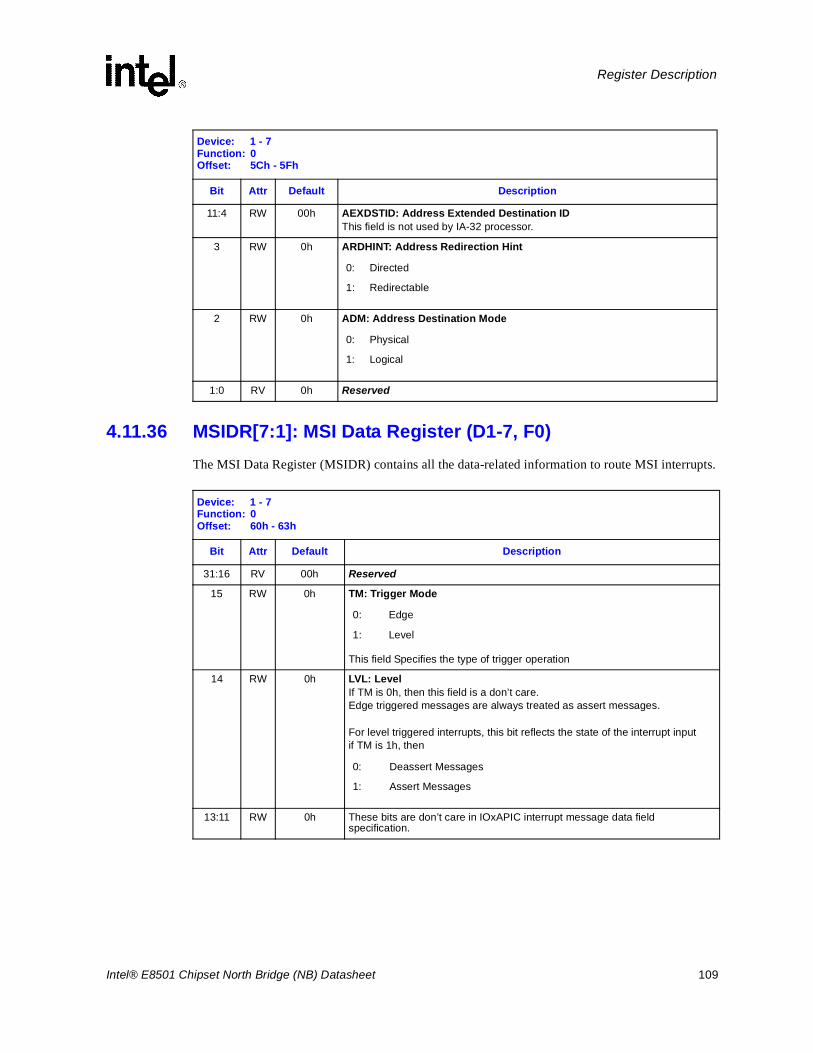
Intel® E8501 Chipset North Bridge (NB) Datasheet 109
Register Description
4.11.36 MSIDR[7:1]: MSI Data Register (D1-7, F0)The MSI Data Register (MSIDR) contains all the data-related information to route MSI interrupts.
11:4 RW 00h AEXDSTID: Address Extended Destination IDThis field is not used by IA-32 processor.
3 RW 0h ARDHINT: Address Redirection Hint
2 RW 0h ADM: Address Destination Mode
1:0 RV 0h Reserved
Device: 1 - 7Function: 0Offset: 5Ch - 5Fh
Bit Attr Default Description
0: Directed
1: Redirectable
0: Physical
1: Logical
Device: 1 - 7Function: 0Offset: 60h - 63h
Bit Attr Default Description
31:16 RV 00h Reserved
15 RW 0h TM: Trigger Mode
This field Specifies the type of trigger operation
14 RW 0h LVL: LevelIf TM is 0h, then this field is a don’t care. Edge triggered messages are always treated as assert messages.
For level triggered interrupts, this bit reflects the state of the interrupt inputif TM is 1h, then
13:11 RW 0h These bits are don’t care in IOxAPIC interrupt message data field specification.
0: Edge
1: Level
0: Deassert Messages
1: Assert Messages
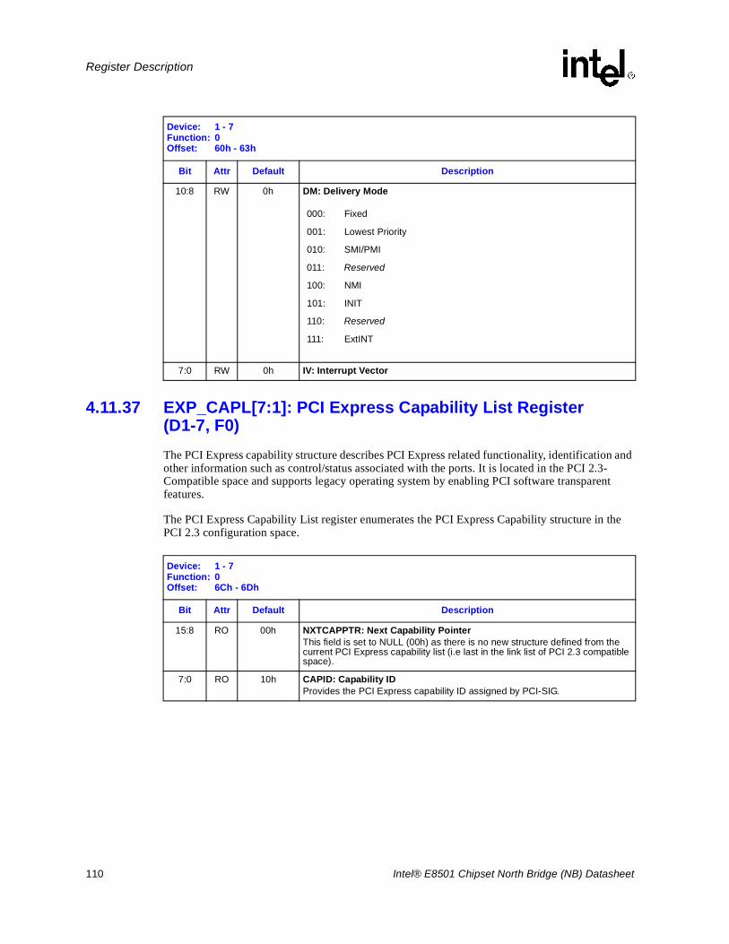
110 Intel® E8501 Chipset North Bridge (NB) Datasheet
Register Description
4.11.37 EXP_CAPL[7:1]: PCI Express Capability List Register (D1-7, F0)The PCI Express capability structure describes PCI Express related functionality, identification and other information such as control/status associated with the ports. It is located in the PCI 2.3-Compatible space and supports legacy operating system by enabling PCI software transparent features.
The PCI Express Capability List register enumerates the PCI Express Capability structure in the PCI 2.3 configuration space.
10:8 RW 0h DM: Delivery Mode
7:0 RW 0h IV: Interrupt Vector
Device: 1 - 7Function: 0Offset: 60h - 63h
Bit Attr Default Description
000: Fixed
001: Lowest Priority
010: SMI/PMI
011: Reserved
100: NMI
101: INIT
110: Reserved
111: ExtINT
Device: 1 - 7Function: 0Offset: 6Ch - 6Dh
Bit Attr Default Description
15:8 RO 00h NXTCAPPTR: Next Capability PointerThis field is set to NULL (00h) as there is no new structure defined from the current PCI Express capability list (i.e last in the link list of PCI 2.3 compatible space).
7:0 RO 10h CAPID: Capability IDProvides the PCI Express capability ID assigned by PCI-SIG.
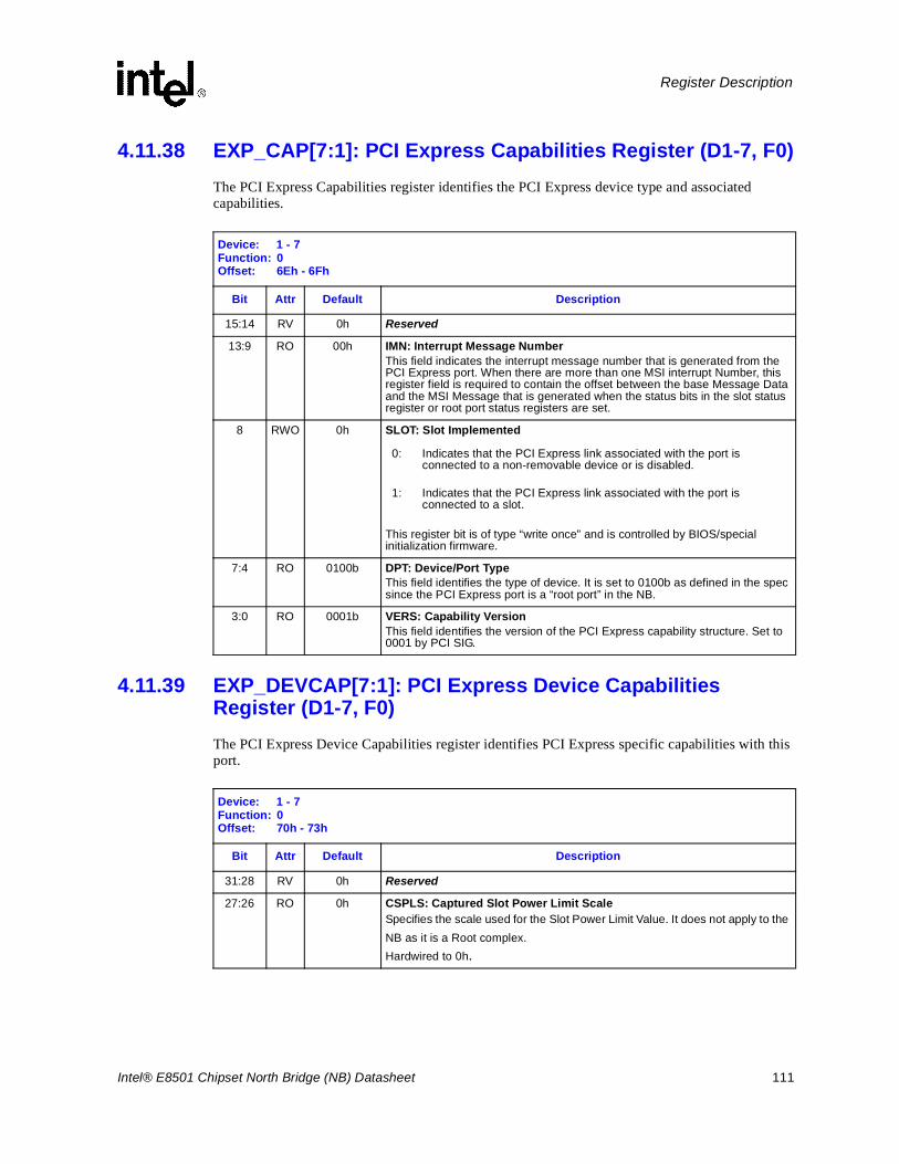
Intel® E8501 Chipset North Bridge (NB) Datasheet 111
Register Description
4.11.38 EXP_CAP[7:1]: PCI Express Capabilities Register (D1-7, F0)The PCI Express Capabilities register identifies the PCI Express device type and associated capabilities.
4.11.39 EXP_DEVCAP[7:1]: PCI Express Device Capabilities Register (D1-7, F0)The PCI Express Device Capabilities register identifies PCI Express specific capabilities with this port.
Device: 1 - 7Function: 0Offset: 6Eh - 6Fh
Bit Attr Default Description
15:14 RV 0h Reserved
13:9 RO 00h IMN: Interrupt Message NumberThis field indicates the interrupt message number that is generated from the PCI Express port. When there are more than one MSI interrupt Number, this register field is required to contain the offset between the base Message Data and the MSI Message that is generated when the status bits in the slot status register or root port status registers are set.
8 RWO 0h SLOT: Slot Implemented
This register bit is of type “write once” and is controlled by BIOS/special initialization firmware.
7:4 RO 0100b DPT: Device/Port TypeThis field identifies the type of device. It is set to 0100b as defined in the spec since the PCI Express port is a “root port” in the NB.
3:0 RO 0001b VERS: Capability VersionThis field identifies the version of the PCI Express capability structure. Set to 0001 by PCI SIG.
0: Indicates that the PCI Express link associated with the port is connected to a non-removable device or is disabled.
1: Indicates that the PCI Express link associated with the port is connected to a slot.
Device: 1 - 7Function: 0Offset: 70h - 73h
Bit Attr Default Description
31:28 RV 0h Reserved
27:26 RO 0h CSPLS: Captured Slot Power Limit Scale Specifies the scale used for the Slot Power Limit Value. It does not apply to the NB as it is a Root complex. Hardwired to 0h.
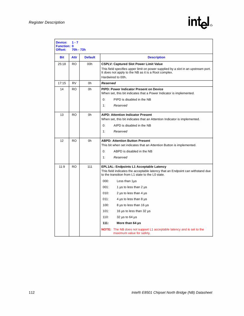
112 Intel® E8501 Chipset North Bridge (NB) Datasheet
Register Description
25:18 RO 00h CSPLV: Captured Slot Power Limit Value This field specifies upper limit on power supplied by a slot in an upstream port. It does not apply to the NB as it is a Root complex. Hardwired to 00h.
17:15 RV 0h Reserved
14 RO 0h PIPD: Power Indicator Present on DeviceWhen set, this bit indicates that a Power Indicator is implemented.
13 RO 0h AIPD: Attention Indicator PresentWhen set, this bit indicates that an Attention Indicator is implemented.
12 RO 0h ABPD: Attention Button PresentThis bit when set indicates that an Attention Button is implemented.
11:9 RO 111 EPL1AL: Endpoints L1 Acceptable LatencyThis field indicates the acceptable latency that an Endpoint can withstand due to the transition from L1 state to the L0 state.
NOTE: The NB does not support L1 acceptable latency and is set to the maximum value for safety.
Device: 1 - 7Function: 0Offset: 70h - 73h
Bit Attr Default Description
0: PIPD is disabled in the NB
1: Reserved
0: AIPD is disabled in the NB
1: Reserved
0: ABPD is disabled in the NB
1: Reserved
000: Less than 1µs
001: 1 µs to less than 2 µs
010: 2 µs to less than 4 µs
011: 4 µs to less than 8 µs
100: 8 µs to less than 16 µs
101: 16 µs to less than 32 µs
110: 32 µs to 64 µs
111: More than 64 µs
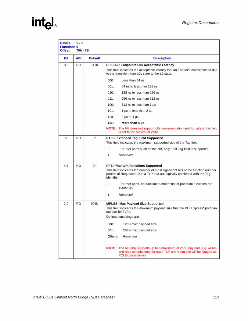
Intel® E8501 Chipset North Bridge (NB) Datasheet 113
Register Description
8:6 RO 111b EPL0AL: Endpoints L0s Acceptable LatencyThis field indicates the acceptable latency that an Endpoint can withstand due to the transition from L0s state to the L0 state.
NOTE: The NB does not support L0s implementation and for safety, this field is set to the maximum value.
5 RO 0h ETFS: Extended Tag Field SupportedThis field indicates the maximum supported size of the Tag field.
4:3 RO 0h PFS: Phantom Functions SupportedThis field indicates the number of most significant bits of the function number portion of Requester ID in a TLP that are logically combined with the Tag identifier.
2:0 RO 001b MPLSS: Max Payload Size SupportedThis field indicates the maximum payload size that the PCI Express* port can support for TLPs.Defined encodings are:
NOTE: The NB only supports up to a maximum of 256B payload (e.g. writes and read completions) for each TLP and violations will be flagged as PCI Express errors.
Device: 1 - 7Function: 0Offset: 70h - 73h
Bit Attr Default Description
000: Less than 64 ns
001: 64 ns to less than 128 ns
010: 128 ns to less than 256 ns
011: 256 ns to less than 512 ns
100: 512 ns to less than 1 µs
101: 1 µs to less than 2 µs
110: 2 µs to 4 µs
111: More than 4 µs
0: For root ports such as the NB, only 5-bit Tag field is supported
1: Reserved
0: For root ports, no function number bits for phantom functions are supported
1: Reserved
000: 128B max payload size
001: 256B max payload size
Others: Reserved
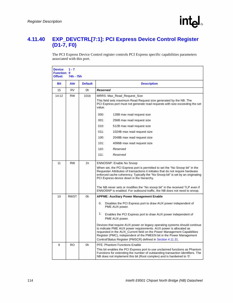
114 Intel® E8501 Chipset North Bridge (NB) Datasheet
Register Description
4.11.40 EXP_DEVCTRL[7:1]: PCI Express Device Control Register(D1-7, F0)The PCI Express Device Control register controls PCI Express specific capabilities parameters associated with this port.
Device: 1 - 7Function: 0Offset: 74h - 75h
Bit Attr Default Description
15 RV 0h Reserved
14:12 RW 101b MRRS: Max_Read_Request_SizeThis field sets maximum Read Request size generated by the NB. The PCI Express port must not generate read requests with size exceeding the set value.
11 RW 1h ENNOSNP: Enable No SnoopWhen set, the PCI Express port is permitted to set the “No Snoop bit” in the Requester Attributes of transactions it initiates that do not require hardware enforced cache coherency. Typically the “No Snoop bit” is set by an originating PCI Express device down in the hierarchy.
The NB never sets or modifies the “No snoop bit” in the received TLP even if ENNOSNP is enabled. For outbound traffic, the NB does not need to snoop.
10 RWST 0h APPME: Auxiliary Power Management Enable
Devices that require AUX power on legacy operating systems should continue to indicate PME AUX power requirements. AUX power is allocated as requested in the AUX_Current field on the Power Management Capabilities Register (PMC), independent of the PMEEN bit in the Power ManagementControl/Status Register (PMSCR) defined in Section 4.11.31.
9 RO 0h PFE: Phantom Functions EnableThis bit enables the PCI Express port to use unclaimed functions as Phantom Functions for extending the number of outstanding transaction identifiers. The NB does not implement this bit (Root complex) and is hardwired to ‘0’.
000: 128B max read request size
001: 256B max read request size
010: 512B max read request size
011: 1024B max read request size
100: 2048B max read request size
101: 4096B max read request size
110: Reserved
111: Reserved
0: Disables the PCI Express port to draw AUX power independent of PME AUX power.
1: Enables the PCI Express port to draw AUX power independent of PME AUX power.
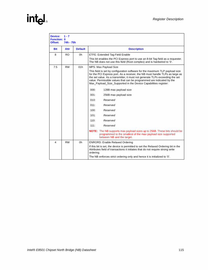
Intel® E8501 Chipset North Bridge (NB) Datasheet 115
Register Description
8 RO 0h ETFE: Extended Tag Field EnableThis bit enables the PCI Express port to use an 8-bit Tag field as a requester. The NB does not use this field (Root complex) and is hardwired to ‘0’.
7:5 RW 01h MPS: Max Payload SizeThis field is set by configuration software for the maximum TLP payload size for the PCI Express port. As a receiver, the NB must handle TLPs as large as the set value. As a transmitter, it must not generate TLPs exceeding the set value. Permissible values that can be programmed are indicated by the Max_Payload_Size_Supported in the Device Capabilities register:
NOTE: The NB supports max payload sizes up to 256B. These bits should be programmed to the smallest of the max payload size supported between NB and the target.
4 RW 0h ENRORD: Enable Relaxed OrderingIf this bit is set, the device is permitted to set the Relaxed Ordering bit in the Attributes field of transactions it initiates that do not require strong write ordering.The NB enforces strict ordering only and hence it is initialized to ‘0’.
Device: 1 - 7Function: 0Offset: 74h - 75h
Bit Attr Default Description
000: 128B max payload size
001: 256B max payload size
010: Reserved
011: Reserved
100: Reserved
101: Reserved
110: Reserved
111: Reserved
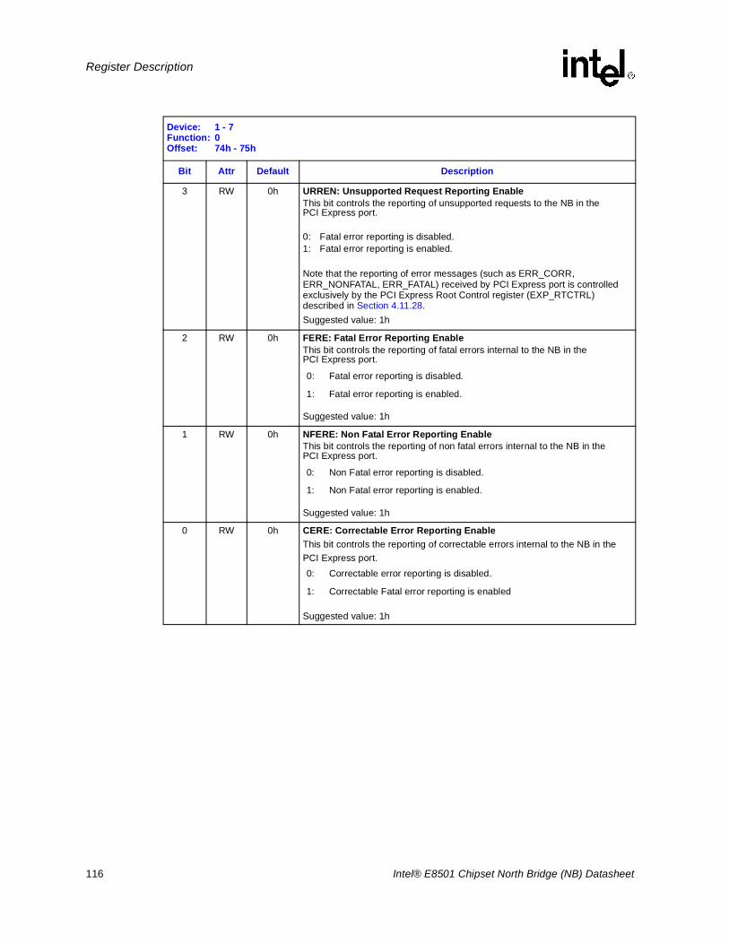
116 Intel® E8501 Chipset North Bridge (NB) Datasheet
Register Description
3 RW 0h URREN: Unsupported Request Reporting EnableThis bit controls the reporting of unsupported requests to the NB in the PCI Express port.
0: Fatal error reporting is disabled.1: Fatal error reporting is enabled.
Note that the reporting of error messages (such as ERR_CORR, ERR_NONFATAL, ERR_FATAL) received by PCI Express port is controlled exclusively by the PCI Express Root Control register (EXP_RTCTRL) described in Section 4.11.28.Suggested value: 1h
2 RW 0h FERE: Fatal Error Reporting EnableThis bit controls the reporting of fatal errors internal to the NB in the PCI Express port.
Suggested value: 1h
1 RW 0h NFERE: Non Fatal Error Reporting EnableThis bit controls the reporting of non fatal errors internal to the NB in the PCI Express port.
Suggested value: 1h
0 RW 0h CERE: Correctable Error Reporting EnableThis bit controls the reporting of correctable errors internal to the NB in the PCI Express port.
Suggested value: 1h
Device: 1 - 7Function: 0Offset: 74h - 75h
Bit Attr Default Description
0: Fatal error reporting is disabled.
1: Fatal error reporting is enabled.
0: Non Fatal error reporting is disabled.
1: Non Fatal error reporting is enabled.
0: Correctable error reporting is disabled.
1: Correctable Fatal error reporting is enabled
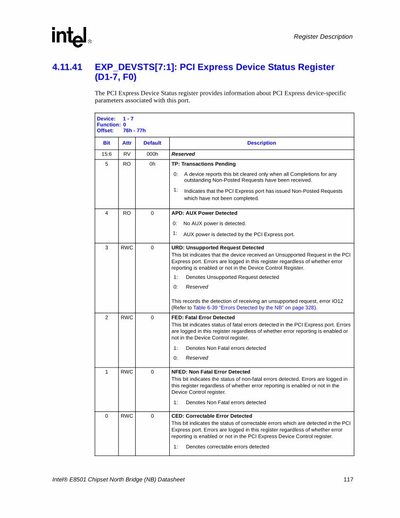
Intel® E8501 Chipset North Bridge (NB) Datasheet 117
Register Description
4.11.41 EXP_DEVSTS[7:1]: PCI Express Device Status Register (D1-7, F0)The PCI Express Device Status register provides information about PCI Express device-specific parameters associated with this port.
Device: 1 - 7Function: 0Offset: 76h - 77h
Bit Attr Default Description
15:6 RV 000h Reserved
5 RO 0h TP: Transactions Pending
4 RO 0 APD: AUX Power Detected
3 RWC 0 URD: Unsupported Request DetectedThis bit indicates that the device received an Unsupported Request in the PCI Express port. Errors are logged in this register regardless of whether error reporting is enabled or not in the Device Control Register.
This records the detection of receiving an unsupported request, error IO12 (Refer to Table 6-39 “Errors Detected by the NB” on page 328).
2 RWC 0 FED: Fatal Error DetectedThis bit indicates status of fatal errors detected in the PCI Express port. Errors are logged in this register regardless of whether error reporting is enabled or not in the Device Control register.
1 RWC 0 NFED: Non Fatal Error DetectedThis bit indicates the status of non-fatal errors detected. Errors are logged in this register regardless of whether error reporting is enabled or not in the Device Control register.
0 RWC 0 CED: Correctable Error DetectedThis bit indicates the status of correctable errors which are detected in the PCI Express port. Errors are logged in this register regardless of whether error reporting is enabled or not in the PCI Express Device Control register.
0: A device reports this bit cleared only when all Completions for any outstanding Non-Posted Requests have been received.
1: Indicates that the PCI Express port has issued Non-Posted Requests which have not been completed.
0: No AUX power is detected.
1: AUX power is detected by the PCI Express port.
1: Denotes Unsupported Request detected
0: Reserved
1: Denotes Non Fatal errors detected
0: Reserved
1: Denotes Non Fatal errors detected
1: Denotes correctable errors detected
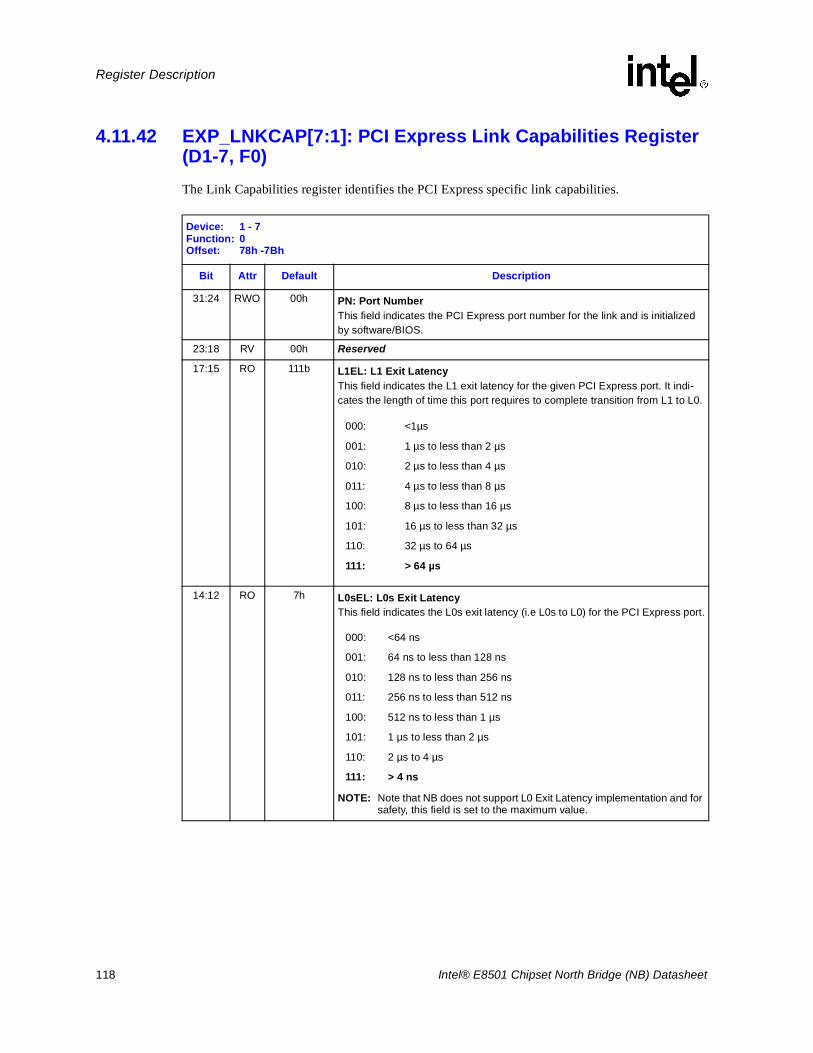
118 Intel® E8501 Chipset North Bridge (NB) Datasheet
Register Description
4.11.42 EXP_LNKCAP[7:1]: PCI Express Link Capabilities Register (D1-7, F0)The Link Capabilities register identifies the PCI Express specific link capabilities.
Device: 1 - 7Function: 0Offset: 78h -7Bh
Bit Attr Default Description
31:24 RWO 00h PN: Port Number This field indicates the PCI Express port number for the link and is initialized by software/BIOS.
23:18 RV 00h Reserved
17:15 RO 111b L1EL: L1 Exit LatencyThis field indicates the L1 exit latency for the given PCI Express port. It indi-cates the length of time this port requires to complete transition from L1 to L0.
14:12 RO 7h L0sEL: L0s Exit Latency This field indicates the L0s exit latency (i.e L0s to L0) for the PCI Express port.
NOTE: Note that NB does not support L0 Exit Latency implementation and for safety, this field is set to the maximum value.
000: <1µs
001: 1 µs to less than 2 µs
010: 2 µs to less than 4 µs
011: 4 µs to less than 8 µs
100: 8 µs to less than 16 µs
101: 16 µs to less than 32 µs
110: 32 µs to 64 µs
111: > 64 µs
000: <64 ns
001: 64 ns to less than 128 ns
010: 128 ns to less than 256 ns
011: 256 ns to less than 512 ns
100: 512 ns to less than 1 µs
101: 1 µs to less than 2 µs
110: 2 µs to 4 µs
111: > 4 ns
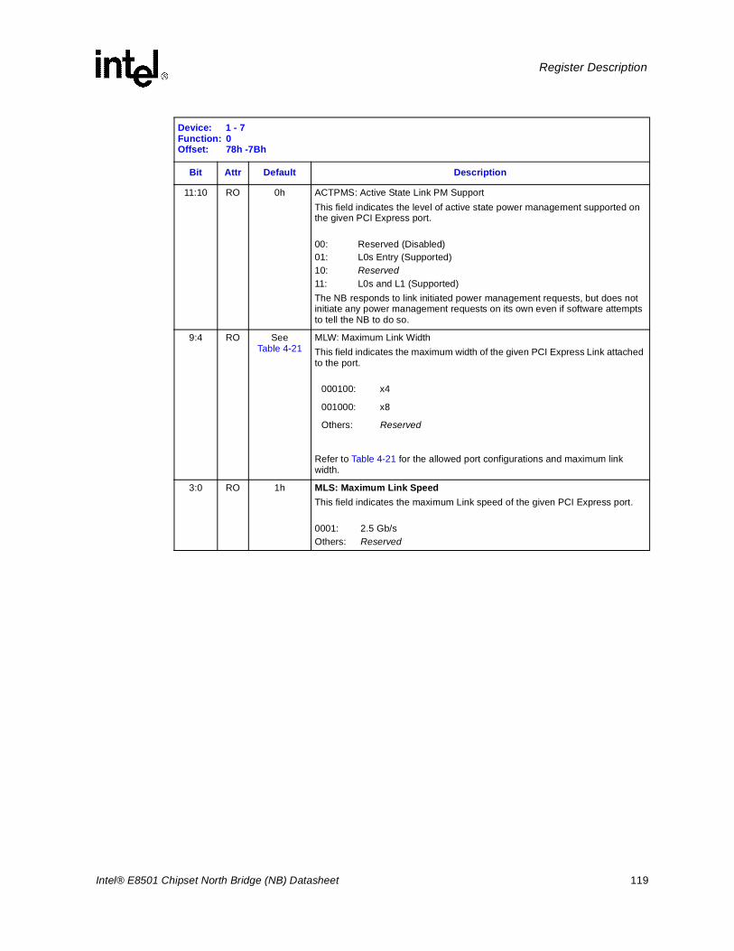
Intel® E8501 Chipset North Bridge (NB) Datasheet 119
Register Description
11:10 RO 0h ACTPMS: Active State Link PM Support This field indicates the level of active state power management supported on the given PCI Express port.
00: Reserved (Disabled)01: L0s Entry (Supported)10: Reserved11: L0s and L1 (Supported)The NB responds to link initiated power management requests, but does not initiate any power management requests on its own even if software attempts to tell the NB to do so.
9:4 RO See Table 4-21
MLW: Maximum Link WidthThis field indicates the maximum width of the given PCI Express Link attached to the port.
Refer to Table 4-21 for the allowed port configurations and maximum link width.
3:0 RO 1h MLS: Maximum Link SpeedThis field indicates the maximum Link speed of the given PCI Express port.
0001: 2.5 Gb/sOthers: Reserved
Device: 1 - 7Function: 0Offset: 78h -7Bh
Bit Attr Default Description
000100: x4
001000: x8
Others: Reserved
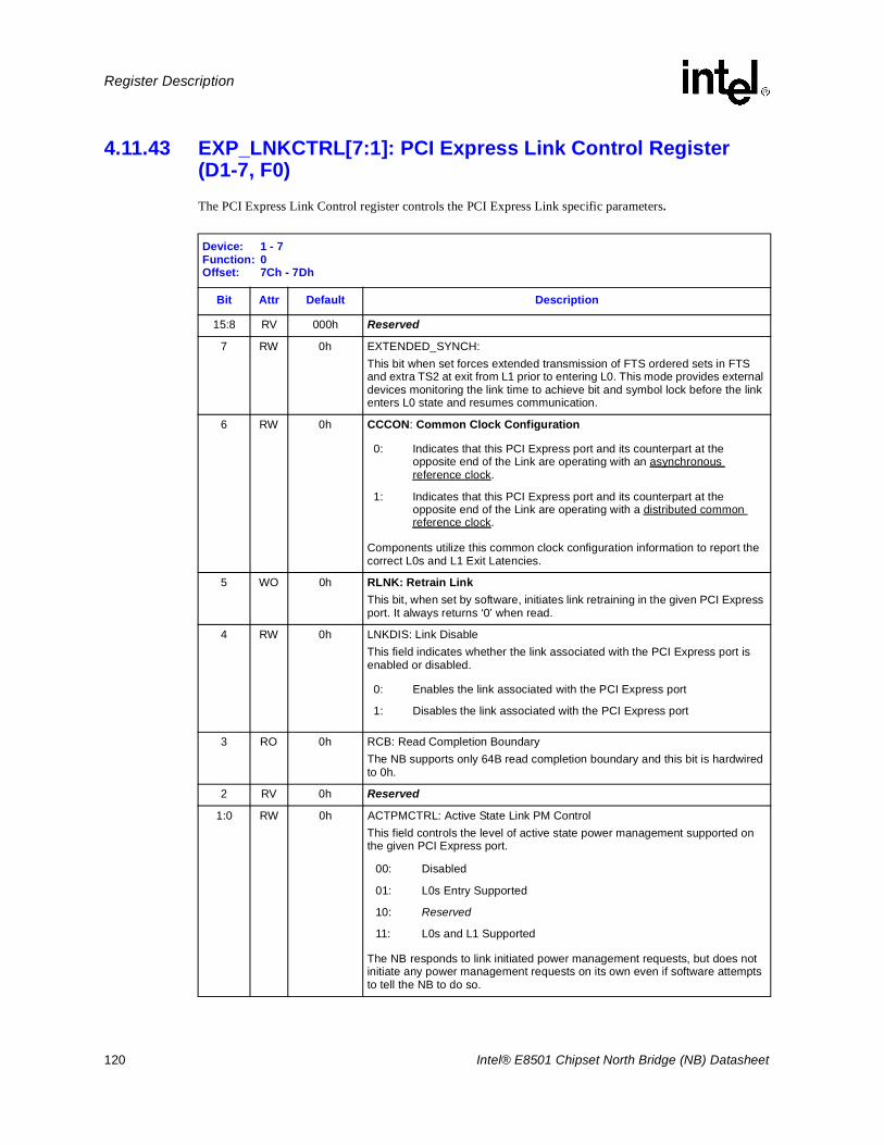
120 Intel® E8501 Chipset North Bridge (NB) Datasheet
Register Description
4.11.43 EXP_LNKCTRL[7:1]: PCI Express Link Control Register(D1-7, F0)The PCI Express Link Control register controls the PCI Express Link specific parameters.
Device: 1 - 7Function: 0Offset: 7Ch - 7Dh
Bit Attr Default Description
15:8 RV 000h Reserved
7 RW 0h EXTENDED_SYNCH: This bit when set forces extended transmission of FTS ordered sets in FTS and extra TS2 at exit from L1 prior to entering L0. This mode provides external devices monitoring the link time to achieve bit and symbol lock before the link enters L0 state and resumes communication.
6 RW 0h CCCON: Common Clock Configuration
Components utilize this common clock configuration information to report the correct L0s and L1 Exit Latencies.
5 WO 0h RLNK: Retrain LinkThis bit, when set by software, initiates link retraining in the given PCI Express port. It always returns ‘0’ when read.
4 RW 0h LNKDIS: Link Disable This field indicates whether the link associated with the PCI Express port is enabled or disabled.
3 RO 0h RCB: Read Completion BoundaryThe NB supports only 64B read completion boundary and this bit is hardwired to 0h.
2 RV 0h Reserved
1:0 RW 0h ACTPMCTRL: Active State Link PM ControlThis field controls the level of active state power management supported on the given PCI Express port.
The NB responds to link initiated power management requests, but does not initiate any power management requests on its own even if software attempts to tell the NB to do so.
0: Indicates that this PCI Express port and its counterpart at the opposite end of the Link are operating with an asynchronous reference clock.
1: Indicates that this PCI Express port and its counterpart at the opposite end of the Link are operating with a distributed common reference clock.
0: Enables the link associated with the PCI Express port
1: Disables the link associated with the PCI Express port
00: Disabled
01: L0s Entry Supported
10: Reserved
11: L0s and L1 Supported
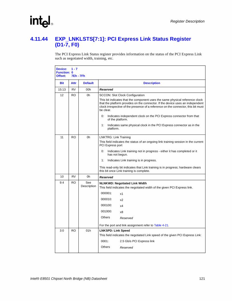
Intel® E8501 Chipset North Bridge (NB) Datasheet 121
Register Description
4.11.44 EXP_LNKLSTS[7:1]: PCI Express Link Status Register (D1-7, F0)The PCI Express Link Status register provides information on the status of the PCI Express Link such as negotiated width, training, etc.
Device: 1 - 7 Function: 0Offset: 7Eh - 7Fh
Bit Attr Default Description
15:13 RV 00h Reserved
12 RO 0h SCCON: Slot Clock ConfigurationThis bit indicates that the component uses the same physical reference clock that the platform provides on the connector. If the device uses an independent clock irrespective of the presence of a reference on the connector, this bit must be clear.
11 RO 0h LNKTRG: Link TrainingThis field indicates the status of an ongoing link training session in the current PCI Express port
This read-only bit indicates that Link training is in progress; hardware clears this bit once Link training is complete.
10 RV 0h Reserved
9:4 RO See Description
NLNKWD: Negotiated Link WidthThis field indicates the negotiated width of the given PCI Express link.
For the port and link assignment refer to Table 4-21.
3:0 RO 01h LNKSPD: Link SpeedThis field indicates the negotiated Link speed of the given PCI Express Link:
0: Indicates independent clock on the PCI Express connector from that of the platform.
1: Indicates same physical clock in the PCI Express connector as in the platform.
0: Indicates Link training not in progress - either it has completed or it has not begun.
1: Indicates Link training is in progress.
000001: x1
000010: x2
000100: x4
001000: x8
Others Reserved
0001: 2.5 Gb/s PCI Express link
Others Reserved
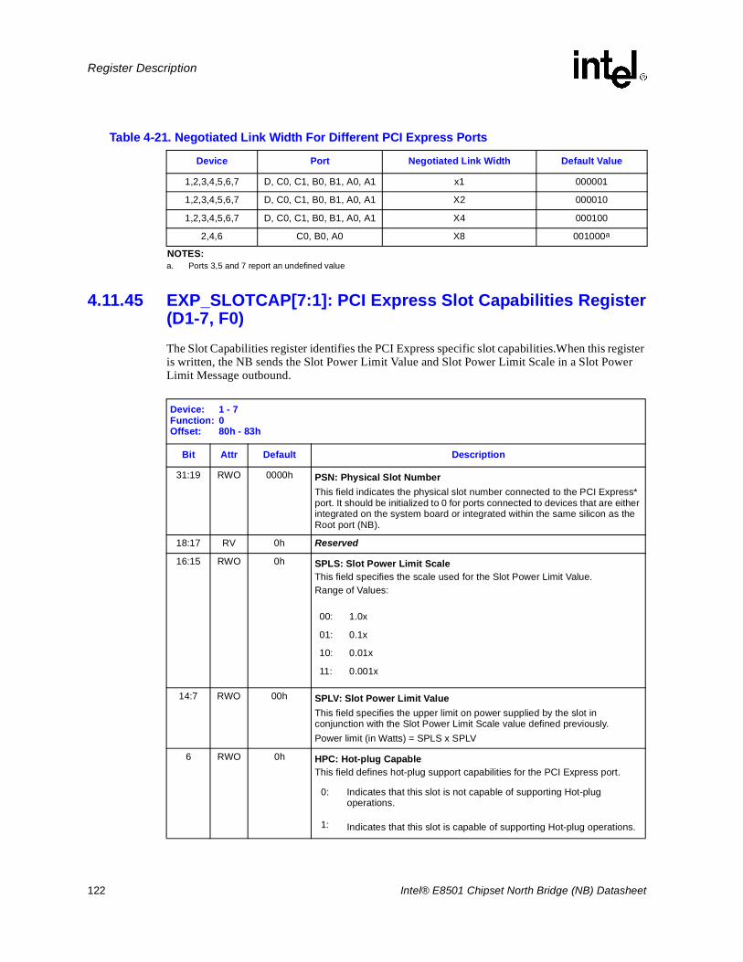
122 Intel® E8501 Chipset North Bridge (NB) Datasheet
Register Description
4.11.45 EXP_SLOTCAP[7:1]: PCI Express Slot Capabilities Register(D1-7, F0)The Slot Capabilities register identifies the PCI Express specific slot capabilities.When this register is written, the NB sends the Slot Power Limit Value and Slot Power Limit Scale in a Slot Power Limit Message outbound.
Table 4-21. Negotiated Link Width For Different PCI Express Ports
Device Port Negotiated Link Width Default Value
1,2,3,4,5,6,7 D, C0, C1, B0, B1, A0, A1 x1 000001
1,2,3,4,5,6,7 D, C0, C1, B0, B1, A0, A1 X2 000010
1,2,3,4,5,6,7 D, C0, C1, B0, B1, A0, A1 X4 000100
2,4,6 C0, B0, A0 X8 001000a
NOTES:a. Ports 3,5 and 7 report an undefined value
Device: 1 - 7 Function: 0Offset: 80h - 83h
Bit Attr Default Description
31:19 RWO 0000h PSN: Physical Slot Number This field indicates the physical slot number connected to the PCI Express* port. It should be initialized to 0 for ports connected to devices that are either integrated on the system board or integrated within the same silicon as the Root port (NB).
18:17 RV 0h Reserved
16:15 RWO 0h SPLS: Slot Power Limit ScaleThis field specifies the scale used for the Slot Power Limit Value.Range of Values:
14:7 RWO 00h SPLV: Slot Power Limit ValueThis field specifies the upper limit on power supplied by the slot in conjunction with the Slot Power Limit Scale value defined previously.Power limit (in Watts) = SPLS x SPLV
6 RWO 0h HPC: Hot-plug Capable This field defines hot-plug support capabilities for the PCI Express port.
00: 1.0x
01: 0.1x
10: 0.01x
11: 0.001x
0: Indicates that this slot is not capable of supporting Hot-plug operations.
1: Indicates that this slot is capable of supporting Hot-plug operations.
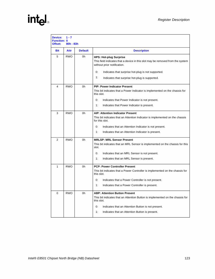
Intel® E8501 Chipset North Bridge (NB) Datasheet 123
Register Description
5 RWO 0h HPS: Hot-plug Surprise This field indicates that a device in this slot may be removed from the system without prior notification.
4 RWO 0h PIP: Power Indicator PresentThis bit indicates that a Power Indicator is implemented on the chassis for this slot.
3 RWO 0h AIP: Attention Indicator PresentThis bit indicates that an Attention Indicator is implemented on the chassis for this slot.
2 RWO 0h MRLSP: MRL Sensor PresentThis bit indicates that an MRL Sensor is implemented on the chassis for this slot.
1 RWO 0h PCP: Power Controller PresentThis bit indicates that a Power Controller is implemented on the chassis for this slot.
0 RWO 0h ABP: Attention Button PresentThis bit indicates that an Attention Button is implemented on the chassis for this slot.
Device: 1 - 7 Function: 0Offset: 80h - 83h
Bit Attr Default Description
0: Indicates that surprise hot-plug is not supported.
1: Indicates that surprise hot-plug is supported.
0: Indicates that Power Indicator is not present.
1: Indicates that Power Indicator is present.
0: Indicates that an Attention Indicator is not present.
1: Indicates that an Attention Indicator is present.
0: Indicates that an MRL Sensor is not present.
1: Indicates that an MRL Sensor is present.
0: Indicates that a Power Controller is not present.
1: Indicates that a Power Controller is present.
0: Indicates that an Attention Button is not present.
1: Indicates that an Attention Button is present.
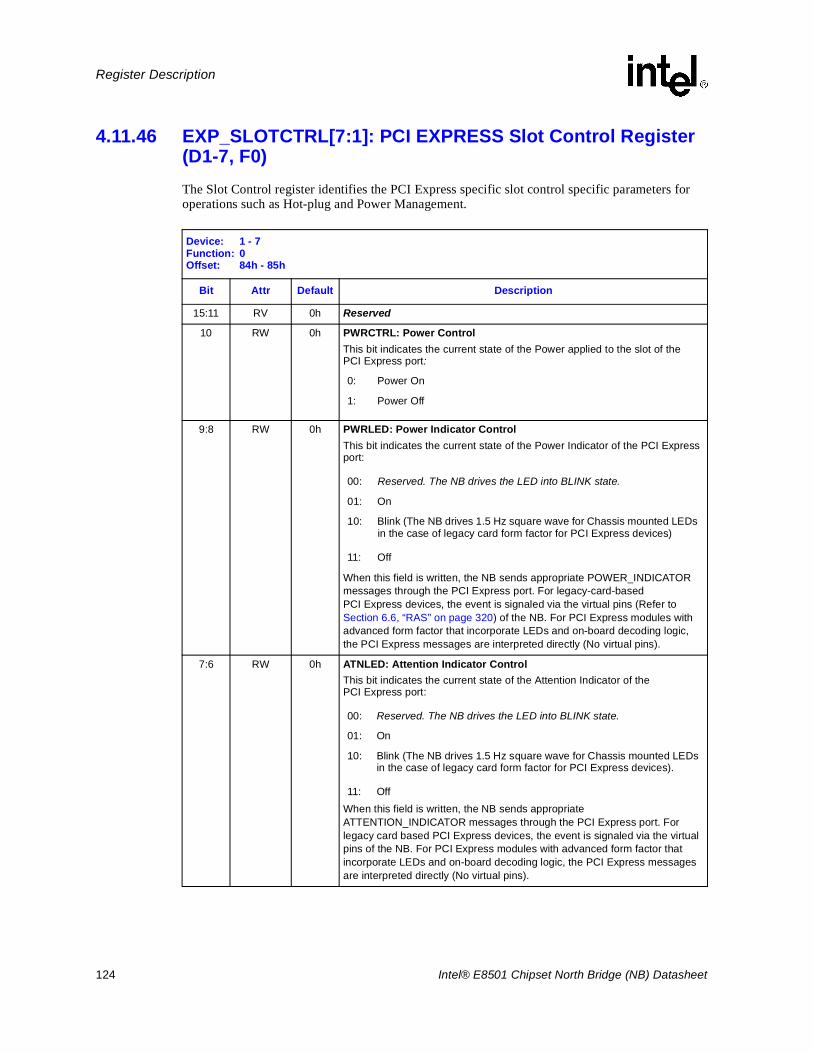
124 Intel® E8501 Chipset North Bridge (NB) Datasheet
Register Description
4.11.46 EXP_SLOTCTRL[7:1]: PCI EXPRESS Slot Control Register(D1-7, F0)The Slot Control register identifies the PCI Express specific slot control specific parameters for operations such as Hot-plug and Power Management.
Device: 1 - 7Function: 0Offset: 84h - 85h
Bit Attr Default Description
15:11 RV 0h Reserved
10 RW 0h PWRCTRL: Power ControlThis bit indicates the current state of the Power applied to the slot of the PCI Express port:
9:8 RW 0h PWRLED: Power Indicator ControlThis bit indicates the current state of the Power Indicator of the PCI Express port:
When this field is written, the NB sends appropriate POWER_INDICATOR messages through the PCI Express port. For legacy-card-based PCI Express devices, the event is signaled via the virtual pins (Refer to Section 6.6, “RAS” on page 320) of the NB. For PCI Express modules with advanced form factor that incorporate LEDs and on-board decoding logic, the PCI Express messages are interpreted directly (No virtual pins).
7:6 RW 0h ATNLED: Attention Indicator ControlThis bit indicates the current state of the Attention Indicator of the PCI Express port:
When this field is written, the NB sends appropriate ATTENTION_INDICATOR messages through the PCI Express port. For legacy card based PCI Express devices, the event is signaled via the virtual pins of the NB. For PCI Express modules with advanced form factor that incorporate LEDs and on-board decoding logic, the PCI Express messages are interpreted directly (No virtual pins).
0: Power On
1: Power Off
00: Reserved. The NB drives the LED into BLINK state.
01: On
10: Blink (The NB drives 1.5 Hz square wave for Chassis mounted LEDs in the case of legacy card form factor for PCI Express devices)
11: Off
00: Reserved. The NB drives the LED into BLINK state.
01: On
10: Blink (The NB drives 1.5 Hz square wave for Chassis mounted LEDs in the case of legacy card form factor for PCI Express devices).
11: Off
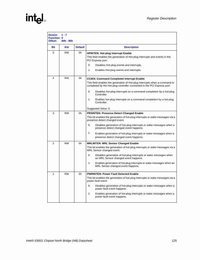
Intel® E8501 Chipset North Bridge (NB) Datasheet 125
Register Description
5 RW 0h HPINTEN: Hot-plug Interrupt EnableThis field enables the generation of Hot-plug interrupts and events in the PCI Express port.
4 RW 0h CCIEN: Command Completed Interrupt EnableThis field enables the generation of Hot-plug interrupts when a command is completed by the Hot-plug controller connected to the PCI Express port:
Suggested Value: 0.
3 RW 0h PRSINTEN: Presence Detect Changed EnableThis bit enables the generation of hot-plug interrupts or wake messages via a presence detect changed event.
2 RW 0h MRLINTEN: MRL Sensor Changed EnableThis bit enables the generation of hot-plug interrupts or wake messages via a MRL Sensor changed event.
1 RW 0h PWRINTEN: Power Fault Detected EnableThis bit enables the generation of hot-plug interrupts or wake messages via a power fault event.
Device: 1 - 7Function: 0Offset: 84h - 85h
Bit Attr Default Description
0: Disables Hot-plug events and interrupts.
1: Enables Hot-plug events and interrupts.
0: Disables hot-plug interrupts on a command completion by a hot-plug Controller.
1: Enables hot-plug interrupts on a command completion by a hot-plug Controller.
0: Disables generation of hot-plug interrupts or wake messages when a presence detect changed event happens.
1: Enables generation of hot-plug interrupts or wake messages when a presence detect changed event happens.
0: Disables generation of hot-plug interrupts or wake messages when an MRL Sensor changed event happens.
1: Enables generation of hot-plug interrupts or wake messages when an MRL Sensor changed event happens.
0: Disables generation of hot-plug interrupts or wake messages when a power fault event happens.
1: Enables generation of hot-plug interrupts or wake messages when a power fault event happens.
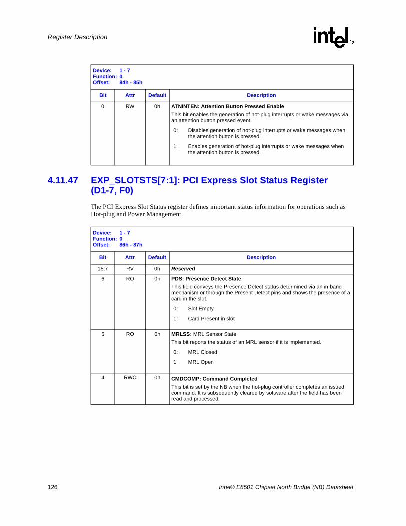
126 Intel® E8501 Chipset North Bridge (NB) Datasheet
Register Description
4.11.47 EXP_SLOTSTS[7:1]: PCI Express Slot Status Register(D1-7, F0)The PCI Express Slot Status register defines important status information for operations such as Hot-plug and Power Management.
0 RW 0h ATNINTEN: Attention Button Pressed EnableThis bit enables the generation of hot-plug interrupts or wake messages via an attention button pressed event.
Device: 1 - 7Function: 0Offset: 84h - 85h
Bit Attr Default Description
0: Disables generation of hot-plug interrupts or wake messages when the attention button is pressed.
1: Enables generation of hot-plug interrupts or wake messages when the attention button is pressed.
Device: 1 - 7Function: 0Offset: 86h - 87h
Bit Attr Default Description
15:7 RV 0h Reserved
6 RO 0h PDS: Presence Detect StateThis field conveys the Presence Detect status determined via an in-band mechanism or through the Present Detect pins and shows the presence of a card in the slot.
5 RO 0h MRLSS: MRL Sensor StateThis bit reports the status of an MRL sensor if it is implemented.
4 RWC 0h CMDCOMP: Command CompletedThis bit is set by the NB when the hot-plug controller completes an issued command. It is subsequently cleared by software after the field has been read and processed.
0: Slot Empty
1: Card Present in slot
0: MRL Closed
1: MRL Open
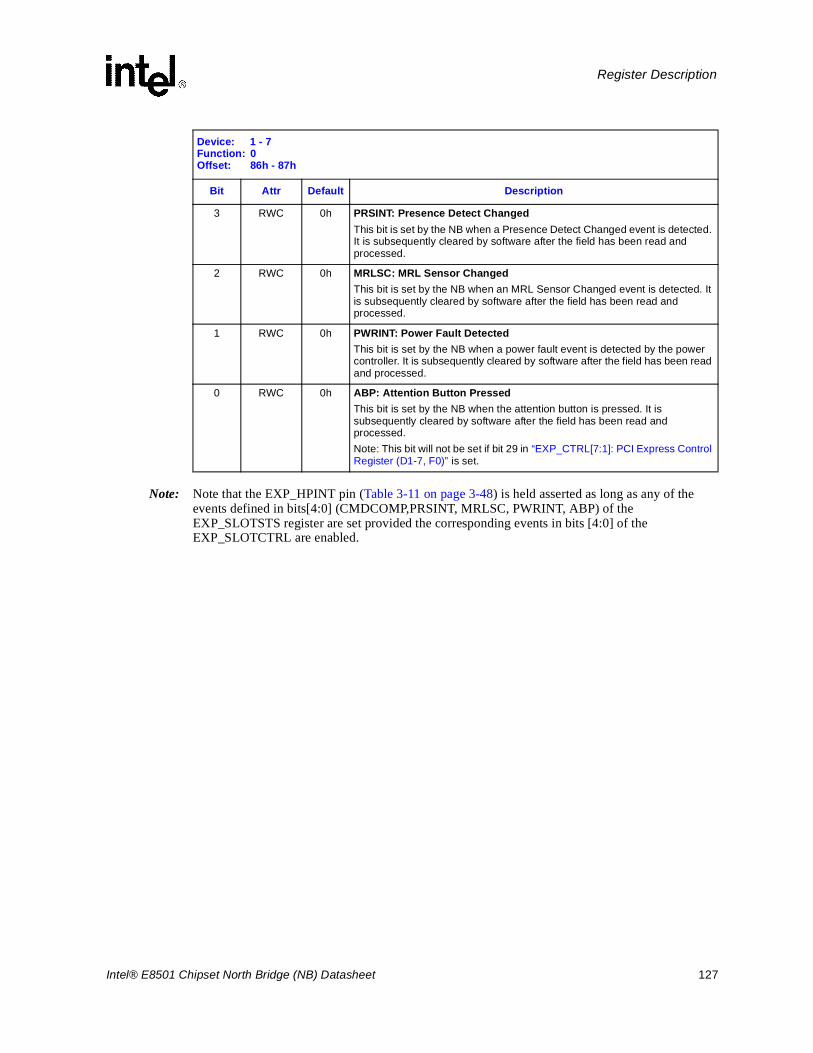
Intel® E8501 Chipset North Bridge (NB) Datasheet 127
Register Description
Note: Note that the EXP_HPINT pin (Table 3-11 on page 3-48) is held asserted as long as any of the events defined in bits[4:0] (CMDCOMP,PRSINT, MRLSC, PWRINT, ABP) of the EXP_SLOTSTS register are set provided the corresponding events in bits [4:0] of the EXP_SLOTCTRL are enabled.
3 RWC 0h PRSINT: Presence Detect ChangedThis bit is set by the NB when a Presence Detect Changed event is detected. It is subsequently cleared by software after the field has been read and processed.
2 RWC 0h MRLSC: MRL Sensor ChangedThis bit is set by the NB when an MRL Sensor Changed event is detected. It is subsequently cleared by software after the field has been read and processed.
1 RWC 0h PWRINT: Power Fault DetectedThis bit is set by the NB when a power fault event is detected by the power controller. It is subsequently cleared by software after the field has been read and processed.
0 RWC 0h ABP: Attention Button PressedThis bit is set by the NB when the attention button is pressed. It is subsequently cleared by software after the field has been read and processed.Note: This bit will not be set if bit 29 in “EXP_CTRL[7:1]: PCI Express Control Register (D1-7, F0)” is set.
Device: 1 - 7Function: 0Offset: 86h - 87h
Bit Attr Default Description
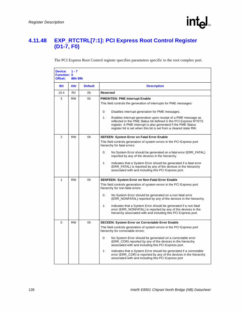
128 Intel® E8501 Chipset North Bridge (NB) Datasheet
Register Description
4.11.48 EXP_RTCTRL[7:1]: PCI Express Root Control Register(D1-7, F0)
The PCI Express Root Control register specifies parameters specific to the root complex port.
Device: 1 - 7Function: 0Offset: 88h 89h
Bit Attr Default Description
15:4 RV 0h Reserved
3 RW 0h PMEINTEN: PME Interrupt EnableThis field controls the generation of interrupts for PME messages:
2 RW 0h SEFEEN: System Error on Fatal Error EnableThis field controls generation of system errors in the PCI Express port hierarchy for fatal errors:
1 RW 0h SENFEEN: System Error on Non-Fatal Error EnableThis field controls generation of system errors in the PCI Express port hierarchy for non-fatal errors:
0 RW 0h SECEEN: System Error on Correctable Error EnableThis field controls generation of system errors in the PCI Express port hierarchy for correctable errors:
0: Disables interrupt generation for PME messages.
1: Enables interrupt generation upon receipt of a PME message as reflected in the PME Status bit defined in the PCI Express RTSTS register. A PME interrupt is also generated if the PME Status register bit is set when this bit is set from a cleared state RW.
0: No System Error should be generated on a fatal error (ERR_FATAL) reported by any of the devices in the hierarchy.
1: Indicates that a System Error should be generated if a fatal error (ERR_FATAL) is reported by any of the devices in the hierarchy associated with and including this PCI Express port.
0: No System Error should be generated on a non-fatal error (ERR_NONFATAL) reported by any of the devices in the hierarchy.
1: indicates that a System Error should be generated if a non-fatal error (ERR_NONFATAL) is reported by any of the devices in the hierarchy associated with and including this PCI Express port.
0: No System Error should be generated on a correctable error (ERR_COR) reported by any of the devices in the hierarchy associated with and including this PCI Express port.
1: Indicates that a System Error should be generated if a correctable error (ERR_COR) is reported by any of the devices in the hierarchy associated with and including this PCI Express port
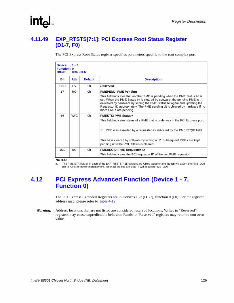
Intel® E8501 Chipset North Bridge (NB) Datasheet 129
Register Description
4.11.49 EXP_RTSTS[7:1]: PCI Express Root Status Register (D1-7, F0)The PCI Express Root Status register specifies parameters specific to the root complex port.
4.12 PCI Express Advanced Function (Device 1 - 7, Function 0)The PCI Express Extended Registers are in Devices 1 -7 (D1-7), function 0 (F0). For the register address map, please refer to Table 4-12.
Warning: Address locations that are not listed are considered reserved locations. Writes to “Reserved” registers may cause unpredictable behavior. Reads to “Reserved” registers may return a non-zero value.
Device: 1 - 7 Function: 0Offset: 8Ch - 8Fh
Bit Attr Default Description
31:18 RV 0h Reserved
17 RO 0h PMEPEND: PME PendingThis field indicates that another PME is pending when the PME Status bit is set. When the PME Status bit is cleared by software, the pending PME is delivered by hardware by setting the PME Status bit again and updating the Requestor ID appropriately. The PME pending bit is cleared by hardware if no more PMEs are pending.
16 RWC 0h PMESTS: PME Statusa
This field indicates status of a PME that is underway in the PCI Express port:
1: PME was asserted by a requester as indicated by the PMEREQID field.
This bit is cleared by software by writing a ‘1’. Subsequent PMEs are kept pending until the PME Status is cleared.
NOTES:a. The PME STATUS bit in each of the EXP_RTSTS[7:1] registers are ORed together and the NB will assert the PME_OUT
pin to ICH5 for power management. When all the bits are clear, it will deassert PME_OUT.
15:0 RO 0h PMEREQID: PME Requester IDThis field indicates the PCI requester ID of the last PME requestor.
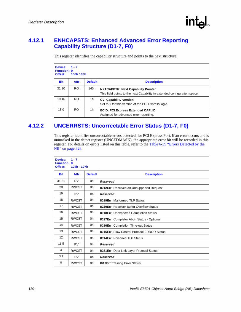
130 Intel® E8501 Chipset North Bridge (NB) Datasheet
Register Description
4.12.1 ENHCAPSTS: Enhanced Advanced Error Reporting Capability Structure (D1-7, F0)This register identifies the capability structure and points to the next structure.
4.12.2 UNCERRSTS: Uncorrectable Error Status (D1-7, F0)This register identifies uncorrectable errors detected. for PCI Express Port. If an error occurs and is unmasked in the detect register (UNCEDMASK), the appropriate error bit will be recorded in this register. For details on errors listed on this table, refer to the Table 6-39 “Errors Detected by the NB” on page 328.
Device: 1 - 7Function: 0Offset: 100h 103h
Bit Attr Default Description
31:20 RO 140h NXTCAPPTR: Next Capability PointerThis field points to the next Capability in extended configuration space.
19:16 RO 1h CV: Capability VersionSet to 1 for this version of the PCI Express logic.
15:0 RO 1h ECID: PCI Express Extended CAP_IDAssigned for advanced error reporting.
Device: 1 - 7Function: 0Offset: 104h - 107h
Bit Attr Default Description
31:21 RV 0h Reserved
20 RWCST 0h IO12Err: Received an Unsupported Request
19 RV 0h Reserved
18 RWCST 0h IO19Err: Malformed TLP Status
17 RWCST 0h IO20Err: Receiver Buffer Overflow Status
16 RWCST 0h IO18Err: Unexpected Completion Status
15 RWCST 0h IO17Err: Completer Abort Status - Optional
14 RWCST 0h IO16Err: Completion Time-out Status
13 RWCST 0h IO15Err: Flow Control Protocol ERROR Status
12 RWCST 0h IO14Err: Poisoned TLP Status
11:5 RV 0h Reserved
4 RWCST 0h IO21Err: Data Link Layer Protocol Status
3:1 RV 0h Reserved
0 RWCST 0h I013Err:Training Error Status
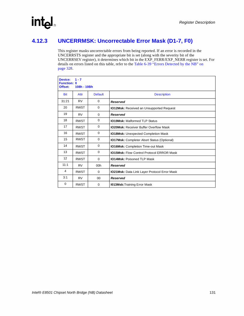
Intel® E8501 Chipset North Bridge (NB) Datasheet 131
Register Description
4.12.3 UNCERRMSK: Uncorrectable Error Mask (D1-7, F0)This register masks uncorrectable errors from being reported. If an error is recorded in the UNCERRSTS register and the appropriate bit is set (along with the severity bit of the UNCERRSEV register), it determines which bit in the EXP_FERR/EXP_NERR register is set. For details on errors listed on this table, refer to the Table 6-39 “Errors Detected by the NB” on page 328.
Device: 1 - 7Function: 0Offset: 108h - 10Bh
Bit Attr Default Description
31:21 RV 0 Reserved
20 RWST 0 IO12Msk: Received an Unsupported Request
19 RV 0 Reserved
18 RWST 0 IO19Msk: Malformed TLP Status
17 RWST 0 IO20Msk: Receiver Buffer Overflow Mask
16 RWST 0 IO18Msk: Unexpected Completion Mask
15 RWST 0 IO17Msk: Completer Abort Status (Optional)
14 RWST 0 IO16Msk: Completion Time-out Mask
13 RWST 0 IO15Msk: Flow Control Protocol ERROR Mask
12 RWST 0 IO14Msk: Poisoned TLP Mask
11:1 RV 00h Reserved
4 RWST 0 IO21Msk: Data Link Layer Protocol Error Mask
3:1 RV 00 Reserved
0 RWST 0 I013Msk:Training Error Mask
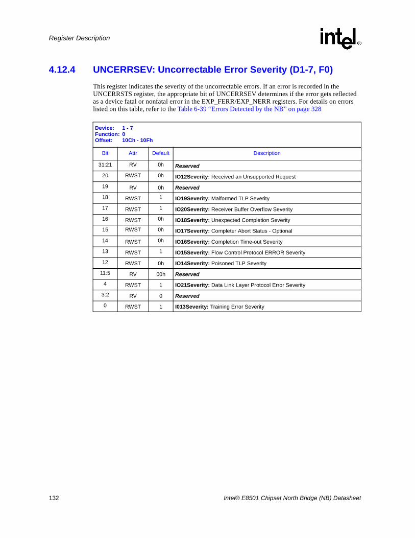
132 Intel® E8501 Chipset North Bridge (NB) Datasheet
Register Description
4.12.4 UNCERRSEV: Uncorrectable Error Severity (D1-7, F0)This register indicates the severity of the uncorrectable errors. If an error is recorded in the UNCERRSTS register, the appropriate bit of UNCERRSEV determines if the error gets reflected as a device fatal or nonfatal error in the EXP_FERR/EXP_NERR registers. For details on errors listed on this table, refer to the Table 6-39 “Errors Detected by the NB” on page 328
Device: 1 - 7Function: 0Offset: 10Ch - 10Fh
Bit Attr Default Description
31:21 RV 0h Reserved
20 RWST 0h IO12Severity: Received an Unsupported Request
19 RV 0h Reserved
18 RWST 1 IO19Severity: Malformed TLP Severity
17 RWST 1 IO20Severity: Receiver Buffer Overflow Severity
16 RWST 0h IO18Severity: Unexpected Completion Severity
15 RWST 0h IO17Severity: Completer Abort Status - Optional
14 RWST 0h IO16Severity: Completion Time-out Severity
13 RWST 1 IO15Severity: Flow Control Protocol ERROR Severity
12 RWST 0h IO14Severity: Poisoned TLP Severity
11:5 RV 00h Reserved
4 RWST 1 IO21Severity: Data Link Layer Protocol Error Severity
3:2 RV 0 Reserved
0 RWST 1 I013Severity: Training Error Severity
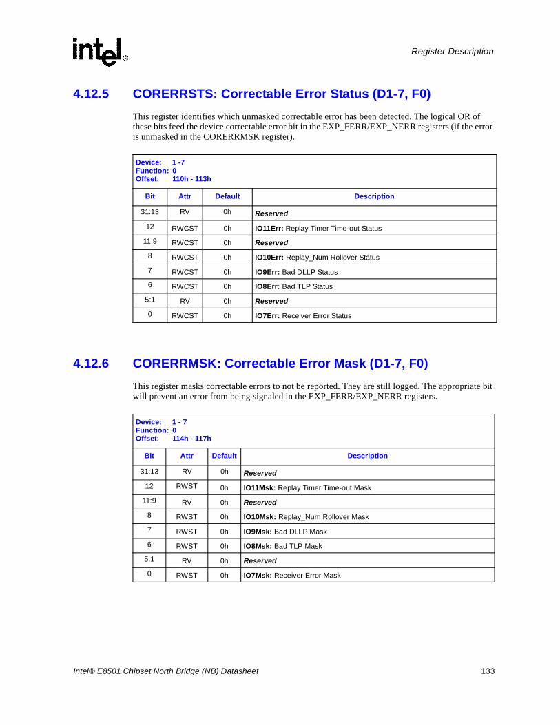
Intel® E8501 Chipset North Bridge (NB) Datasheet 133
Register Description
4.12.5 CORERRSTS: Correctable Error Status (D1-7, F0)This register identifies which unmasked correctable error has been detected. The logical OR of these bits feed the device correctable error bit in the EXP_FERR/EXP_NERR registers (if the error is unmasked in the CORERRMSK register).
4.12.6 CORERRMSK: Correctable Error Mask (D1-7, F0)This register masks correctable errors to not be reported. They are still logged. The appropriate bit will prevent an error from being signaled in the EXP_FERR/EXP_NERR registers.
Device: 1 -7Function: 0Offset: 110h - 113h
Bit Attr Default Description
31:13 RV 0h Reserved
12 RWCST 0h IO11Err: Replay Timer Time-out Status
11:9 RWCST 0h Reserved
8 RWCST 0h IO10Err: Replay_Num Rollover Status
7 RWCST 0h IO9Err: Bad DLLP Status
6 RWCST 0h IO8Err: Bad TLP Status
5:1 RV 0h Reserved
0 RWCST 0h IO7Err: Receiver Error Status
Device: 1 - 7Function: 0Offset: 114h - 117h
Bit Attr Default Description
31:13 RV 0h Reserved
12 RWST 0h IO11Msk: Replay Timer Time-out Mask
11:9 RV 0h Reserved
8 RWST 0h IO10Msk: Replay_Num Rollover Mask
7 RWST 0h IO9Msk: Bad DLLP Mask
6 RWST 0h IO8Msk: Bad TLP Mask
5:1 RV 0h Reserved
0 RWST 0h IO7Msk: Receiver Error Mask
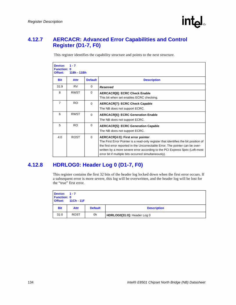
134 Intel® E8501 Chipset North Bridge (NB) Datasheet
Register Description
4.12.7 AERCACR: Advanced Error Capabilities and ControlRegister (D1-7, F0) This register identifies the capability structure and points to the next structure.
4.12.8 HDRLOG0: Header Log 0 (D1-7, F0)This register contains the first 32 bits of the header log locked down when the first error occurs. If a subsequent error is more severe, this log will be overwritten, and the header log will be lost for the “true” first error.
Device: 1 - 7Function: 0Offset: 118h - 11Bh
Bit Attr Default Description
31:9 RV 0 Reserved
8 RWST 0 AERCACR[8]: ECRC Check EnableThis bit when set enables ECRC checking.
7 RO 0 AERCACR[7]: ECRC Check CapableThe NB does not support ECRC.
6 RWST 0 AERCACR[6]: ECRC Generation EnableThe NB does not support ECRC.
5 RO 0 AERCACR[5]: ECRC Generation CapableThe NB does not support ECRC.
4:0 ROST 0 AERCACR[4:0]: First error pointerThe First Error Pointer is a read-only register that identifies the bit position of the first error reported in the Uncorrectable Error. The pointer can be over-written by a more severe error according to the PCI Express Spec (Left-most error bit if multiple bits occurred simultaneously).
Device: 1 - 7Function: 0Offset: 11Ch - 11F
Bit Attr Default Description
31:0 ROST 0h HDRLOG0[31:0]: Header Log 0
Intel® E8501 Chipset North Bridge (NB) Datasheet 135
Register Description
4.12.9 HDRLOG1: Header Log 1 (D1-7, F0)
This register contains the second 32 bits of the header log.
4.12.10 HDRLOG2: Header Log 2 (D1-7, F0)
This register contains the third 32 bits of the header log.
4.12.11 HDRLOG3: Header Log 3 (D1-7, F0)This register contains the fourth 32 bits of the header log.
Device: 1 - 7Function: 0Offset: 120h - 123h
Bit Attr Default Description
31:0 ROST 0h HDRLOG1[31:0]: Header Log 1
Device: 1 -7Function: 0Offset: 124h - 127h
Bit Attr Default Description
31:0 ROST 0h HDRLOG2[31:0]: Header Log 2
Device: 1 - 7 Function: 0Offset: 128h - 12Bh
Bit Attr Default Description
31:0 ROST 0h HDRLOG3[31:0]: Header Log 3
136 Intel® E8501 Chipset North Bridge (NB) Datasheet
Register Description
4.12.12 RPERRCMD: Root Port Error Command (D1-7, F0)This register controls behavior upon detection of errors.
4.12.13 RPERRMSGSTS: Root Port Error Message Status(D1-7, F0)
Device: 1 - 7Function: 0Offset: 12Ch - 12Fh
Bit Attr Default Description
31:8 RV 0h Reserved
7:3 RV 0h Reserved
2 RW 0h RPERRCMD_EN_FAT Enable interrupt on fatal errors when set.
1 RW 0h RPERRCMD_EN_UNCORREnable interrupt on uncorrectable errors when set.
0 RW 0h RPERRCMD_EN_CORREnable interrupt on correctable errors when set.
Device: 1 - 7Function: 0Offset: 130h - 133h
Bit Attr Default Description
31:27 RO 0h RPERRMSGSTS_INT_MSGS[4:0] Advanced Error Interrupt Message Number offset between base message data an the MSI message if assigned more than one message number to be used of any status in this capability.
26:7 RV 0h Reserved
6 RWCST 0h FATAL: Fatal Error Message Detected
5 RWCST 0h NONFATAL: NonFatal Error Message Detected
4 RWCST 0h 1st_UNCOR_FATAL: First Uncorrectable Fatal Error Message Detected
3RWCST 0h RPERRMSGSTS_NXT_UNCORR: Next Uncorrectable Error Message
Detected.
2RWCST 0h RPERRMSGSTS_1ST_UNCORR: First Uncorrectable Error Message
Detected.
1 RWCST 0h RPERRMSGSTS_NXT_CORR: Next Correctable Error Message Detected.
0 RWCST 0h RPERRMSGSTS_1ST_CORR: First Correctable Error Message Detected.
Intel® E8501 Chipset North Bridge (NB) Datasheet 137
Register Description
4.12.14 ERRSID: Error Source ID (D1-7, F0)This register identifies the ID of the first correctable and uncorrectable errors.
4.12.15 NBSPCAPID: NB Specific Capability ID (D1-7, F0)This register identifies the capability structure and points to the next structure.
4.12.16 EXP_unitERR: PCI Express Unit Error Register (D1-7, F0)Host Bridge Error Commands for doing the various signaling: ERR[2:0] and MCERR. These errors correspond to the “unit” errors of the PCI Express block. For details on errors listed on this table, refer to the Table 6-39 “Errors Detected by the NB” on page 328.
Device: 1 - 7Function: 0Offset: 134h - 137h
Bit Attr Default Description
31:16 ROST 0h ERRSID_UNCORR_ID[15:0]: Uncorrectable Error Source IDRequestor ID of the source when an uncorrectable error is received and the First Uncorrectable Error Detected is not already set.
15:0 ROST 0h ERRSID_CORR_ID[15:0]: Correctable Error Source IDRequestor ID of the source when a correctable error is received and the First Correctable Error Detected is not already set.
Device: 1 - 7Function: 0Offset: 140h - 143h
Bit Attr Default Description
31:20 RO 0h NXT_CAP_PTR[11:0]: Next Capability PointerThis field points to the next Capability in extended configuration space.
19:16 RO 0h MCH_VENDOR_ID[3:0]: Version Number
15:0 RO 0h EXT_CAP_ID[15:0]: Extended CAP_ID
Device: 1 - 7Function: 0Offset: 144h - 147h
Bit Attr Default Description
31:4 RV 0h Reserved
3 RWST 0h T9Err: SMBus Virtual Pin Interface Error (FATAL Error)
2 RWST 0h T10Err: I/O Unit Detected Failure (FATAL Error)
1 RWST 0h T2Err: Received an uncorrectable ECC Error from CDC (FATAL Error)
0 RWST 0h T1Err: Received a correctable ECC Error from CDC (Corr. Error)
138 Intel® E8501 Chipset North Bridge (NB) Datasheet
Register Description
4.12.17 EXP_ERR_DOCMD: PCI Express Error Do CommandRegister (D1-7, F0)Link Error Commands for doing the various signaling: ERR[2:0] and MCERR. For this Register usage refer to Figure 6-16 “Error Integration Model” on page 6-327.
Device: 1 - 7Function: 0Offset: 148h - 14Bh
Bit Attr Default Description
31:16 RV 0h Reserved
15 RW 1 COR_RPT_EN: Correctable internal error report enable
14 RW 1 UNC_RPT_EN: Uncorrectable internal error report enable
13:12 RW 01 EXP_RP_FAT_MAP: Root Port steering for fatal errors
If the ERR[2] enable in the Root Command register is set for fatal errors, all fatal errors will be reported via ERR[2] regardless of the setting of this register.MSI enable takes precedence for this capability feature.
11:10 RW 01 EXP_RP_NF_MAP: Root Port steering for non-fatal errors
If the ERR[2] enable in the Root Command register is set for non-fatal errors, all non-fatal errors will be reported via ERR[2] regardless of the setting of this register.MSI enable takes precedence for this capability feature.
1: enable
0: disable
1: enable
0: disable
00: ERR[0]
01: ERR[1]
10: ERR[2]
11: MCERR (This encoding should not be used)
00: ERR[0]
01: ERR[1]
10: ERR[2]
11: MCERR
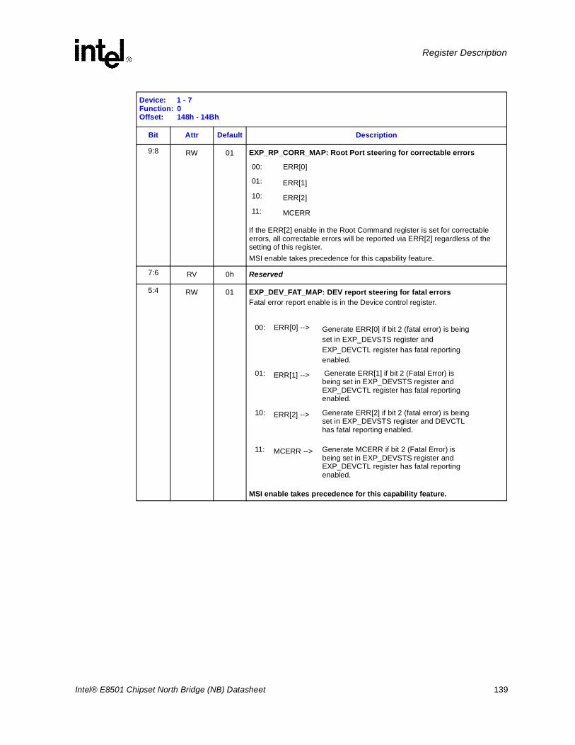
Intel® E8501 Chipset North Bridge (NB) Datasheet 139
Register Description
9:8 RW 01 EXP_RP_CORR_MAP: Root Port steering for correctable errors
If the ERR[2] enable in the Root Command register is set for correctable errors, all correctable errors will be reported via ERR[2] regardless of the setting of this register.MSI enable takes precedence for this capability feature.
7:6 RV 0h Reserved
5:4 RW 01 EXP_DEV_FAT_MAP: DEV report steering for fatal errorsFatal error report enable is in the Device control register.
MSI enable takes precedence for this capability feature.
Device: 1 - 7Function: 0Offset: 148h - 14Bh
Bit Attr Default Description
00: ERR[0]
01: ERR[1]
10: ERR[2]
11: MCERR
00: ERR[0] --> Generate ERR[0] if bit 2 (fatal error) is being set in EXP_DEVSTS register and EXP_DEVCTL register has fatal reporting enabled.
01: ERR[1] --> Generate ERR[1] if bit 2 (Fatal Error) is being set in EXP_DEVSTS register and EXP_DEVCTL register has fatal reporting enabled.
10: ERR[2] --> Generate ERR[2] if bit 2 (fatal error) is being set in EXP_DEVSTS register and DEVCTL has fatal reporting enabled.
11: MCERR --> Generate MCERR if bit 2 (Fatal Error) is being set in EXP_DEVSTS register and EXP_DEVCTL register has fatal reporting enabled.
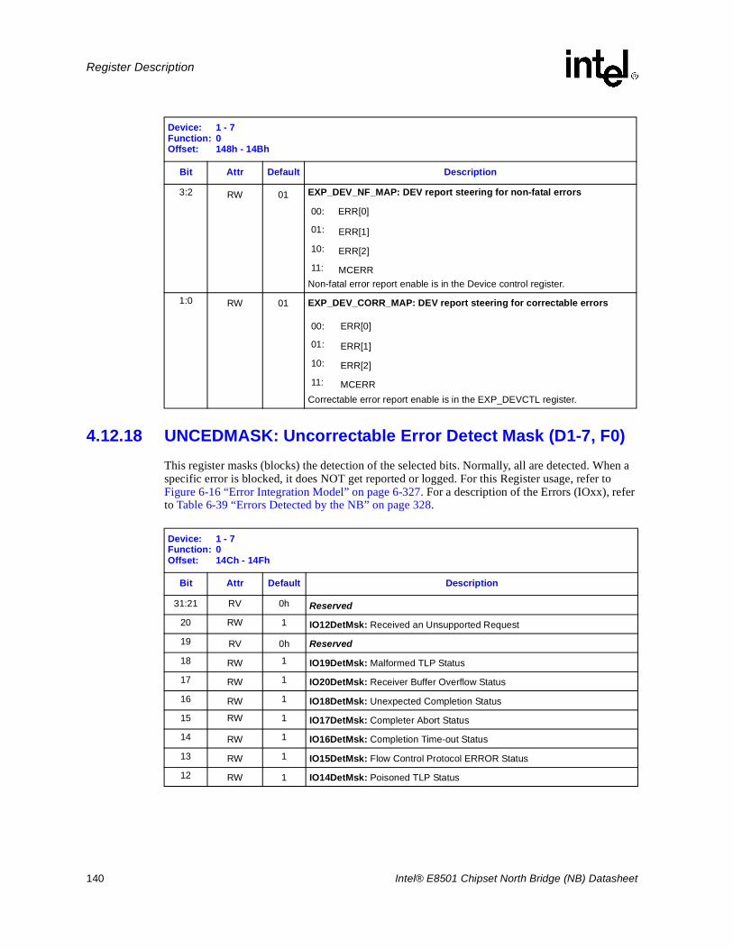
140 Intel® E8501 Chipset North Bridge (NB) Datasheet
Register Description
4.12.18 UNCEDMASK: Uncorrectable Error Detect Mask (D1-7, F0)This register masks (blocks) the detection of the selected bits. Normally, all are detected. When a specific error is blocked, it does NOT get reported or logged. For this Register usage, refer to Figure 6-16 “Error Integration Model” on page 6-327. For a description of the Errors (IOxx), refer to Table 6-39 “Errors Detected by the NB” on page 328.
3:2 RW 01 EXP_DEV_NF_MAP: DEV report steering for non-fatal errors
Non-fatal error report enable is in the Device control register.
1:0 RW 01 EXP_DEV_CORR_MAP: DEV report steering for correctable errors
Correctable error report enable is in the EXP_DEVCTL register.
Device: 1 - 7Function: 0Offset: 148h - 14Bh
Bit Attr Default Description
00: ERR[0]
01: ERR[1]
10: ERR[2]
11: MCERR
00: ERR[0]
01: ERR[1]
10: ERR[2]
11: MCERR
Device: 1 - 7Function: 0Offset: 14Ch - 14Fh
Bit Attr Default Description
31:21 RV 0h Reserved
20 RW 1 IO12DetMsk: Received an Unsupported Request
19 RV 0h Reserved
18 RW 1 IO19DetMsk: Malformed TLP Status
17 RW 1 IO20DetMsk: Receiver Buffer Overflow Status
16 RW 1 IO18DetMsk: Unexpected Completion Status
15 RW 1 IO17DetMsk: Completer Abort Status
14 RW 1 IO16DetMsk: Completion Time-out Status
13 RW 1 IO15DetMsk: Flow Control Protocol ERROR Status
12 RW 1 IO14DetMsk: Poisoned TLP Status
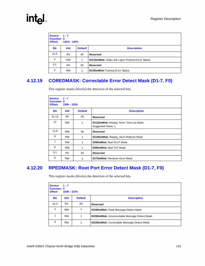
Intel® E8501 Chipset North Bridge (NB) Datasheet 141
Register Description
4.12.19 COREDMASK: Correctable Error Detect Mask (D1-7, F0)This register masks (blocks) the detection of the selected bits.
4.12.20 RPEDMASK: Root Port Error Detect Mask (D1-7, F0)This register masks (blocks) the detection of the selected bits.
11:5 RV 0h Reserved
4 RW 1 IO21DetMsk: Data Link Layer Protocol Error Status
3:1 RV 0h Reserved
0 RW 1 I013DetMsk:Training Error Status
Device: 1 - 7Function: 0Offset: 14Ch - 14Fh
Bit Attr Default Description
Device: 1 - 7Function: 0Offset: 150h - 153h
Bit Attr Default Description
31:13 RV 0h Reserved
12 RW 1 IO11DetMsk: Replay Timer Time-out MaskSuggested Value: 1
11:9 RW 0h Reserved
8 RW 1 IO10DetMsk: Replay_Num Rollover Mask
7 RW 1 IO9DetMsk: Bad DLLP Mask
6 RW 1 IO8DetMsk: Bad TLP Mask
5:1 RV 0h Reserved
0 RW 1 IO7DetMsk: Receiver Error Mask
Device: 1 - 7Function: 0Offset: 154h - 157h
Bit Attr Default Description
31:3 RV 0h Reserved
2 RW 1 IO26DetMsk: Fatal Message Detect Mask
1 RW 1 IO25DetMsk: Uncorrectable Message Detect Mask
0 RW 1 IO24DetMsk: Correctable Message Detect Mask
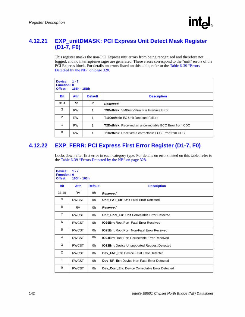
142 Intel® E8501 Chipset North Bridge (NB) Datasheet
Register Description
4.12.21 EXP_unitDMASK: PCI Express Unit Detect Mask Register(D1-7, F0)This register masks the non-PCI Express unit errors from being recognized and therefore not logged, and no interrupt/messages are generated. These errors correspond to the “unit” errors of the PCI Express block. For details on errors listed on this table, refer to the Table 6-39 “Errors Detected by the NB” on page 328.
4.12.22 EXP_FERR: PCI Express First Error Register (D1-7, F0)Locks down after first error in each category type. For details on errors listed on this table, refer to the Table 6-39 “Errors Detected by the NB” on page 328.
Device: 1 - 7Function: 0Offset: 158h - 15Bh
Bit Attr Default Description
31:4 RV 0h Reserved
3 RW 1 T9DetMsk: SMBus Virtual Pin Interface Error
2 RW 1 T10DetMsk: I/O Unit Detected Failure
1 RW 1 T2DetMsk: Received an uncorrectable ECC Error from CDC
0 RW 1 T1DetMsk: Received a correctable ECC Error from CDC
Device: 1 - 7Function: 0Offset: 160h - 163h
Bit Attr Default Description
31:10 RV 0h Reserved
9 RWCST 0h Unit_FAT_Err: Unit Fatal Error Detected
8 RV 0h Reserved
7 RWCST 0h Unit_Corr_Err: Unit Correctable Error Detected
6 RWCST 0h IO26Err: Root Port Fatal Error Received
5 RWCST 0h IO25Err: Root Port Non-Fatal Error Received
4 RWCST 0h IO24Err: Root Port Correctable Error Received
3 RWCST 0h IO12Err: Device Unsupported Request Detected
2 RWCST 0h Dev_FAT_Err: Device Fatal Error Detected
1 RWCST 0h Dev_NF_Err: Device Non-Fatal Error Detected
0 RWCST 0h Dev_Corr_Err: Device Correctable Error Detected
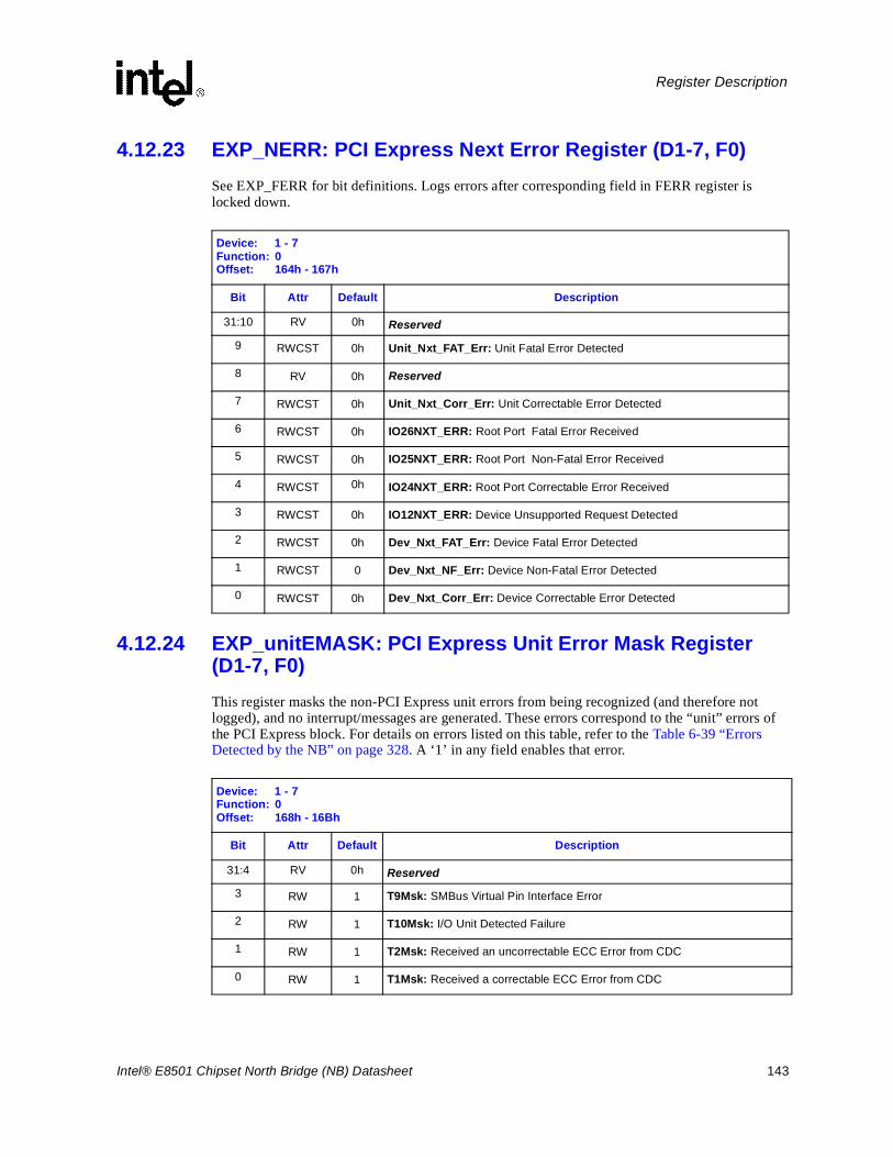
Intel® E8501 Chipset North Bridge (NB) Datasheet 143
Register Description
4.12.23 EXP_NERR: PCI Express Next Error Register (D1-7, F0)See EXP_FERR for bit definitions. Logs errors after corresponding field in FERR register is locked down.
4.12.24 EXP_unitEMASK: PCI Express Unit Error Mask Register (D1-7, F0)This register masks the non-PCI Express unit errors from being recognized (and therefore not logged), and no interrupt/messages are generated. These errors correspond to the “unit” errors of the PCI Express block. For details on errors listed on this table, refer to the Table 6-39 “Errors Detected by the NB” on page 328. A ‘1’ in any field enables that error.
Device: 1 - 7Function: 0Offset: 164h - 167h
Bit Attr Default Description
31:10 RV 0h Reserved
9 RWCST 0h Unit_Nxt_FAT_Err: Unit Fatal Error Detected
8 RV 0h Reserved
7 RWCST 0h Unit_Nxt_Corr_Err: Unit Correctable Error Detected
6 RWCST 0h IO26NXT_ERR: Root Port Fatal Error Received
5 RWCST 0h IO25NXT_ERR: Root Port Non-Fatal Error Received
4 RWCST 0h IO24NXT_ERR: Root Port Correctable Error Received
3 RWCST 0h IO12NXT_ERR: Device Unsupported Request Detected
2 RWCST 0h Dev_Nxt_FAT_Err: Device Fatal Error Detected
1 RWCST 0 Dev_Nxt_NF_Err: Device Non-Fatal Error Detected
0 RWCST 0h Dev_Nxt_Corr_Err: Device Correctable Error Detected
Device: 1 - 7Function: 0Offset: 168h - 16Bh
Bit Attr Default Description
31:4 RV 0h Reserved
3 RW 1 T9Msk: SMBus Virtual Pin Interface Error
2 RW 1 T10Msk: I/O Unit Detected Failure
1 RW 1 T2Msk: Received an uncorrectable ECC Error from CDC
0 RW 1 T1Msk: Received a correctable ECC Error from CDC
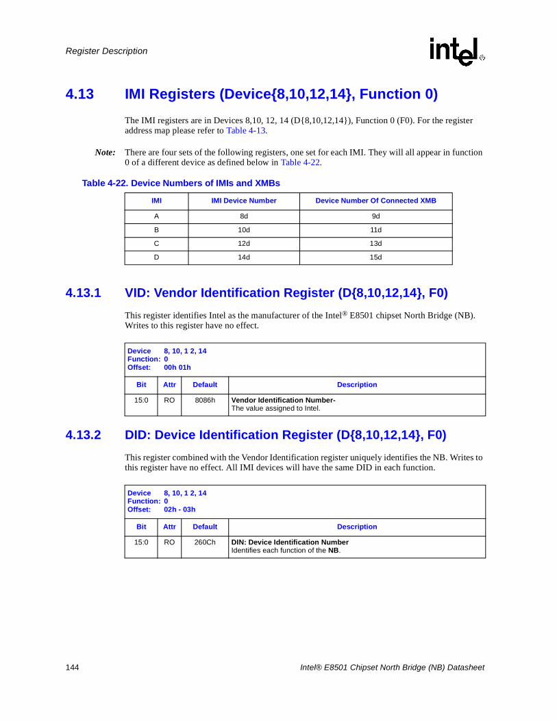
144 Intel® E8501 Chipset North Bridge (NB) Datasheet
Register Description
4.13 IMI Registers (Device{8,10,12,14}, Function 0)The IMI registers are in Devices 8,10, 12, 14 (D{8,10,12,14}), Function 0 (F0). For the register address map please refer to Table 4-13.
Note: There are four sets of the following registers, one set for each IMI. They will all appear in function 0 of a different device as defined below in Table 4-22.
.
4.13.1 VID: Vendor Identification Register (D{8,10,12,14}, F0)This register identifies Intel as the manufacturer of the Intel® E8501 chipset North Bridge (NB). Writes to this register have no effect.
4.13.2 DID: Device Identification Register (D{8,10,12,14}, F0)This register combined with the Vendor Identification register uniquely identifies the NB. Writes to this register have no effect. All IMI devices will have the same DID in each function.
Table 4-22. Device Numbers of IMIs and XMBs
IMI IMI Device Number Device Number Of Connected XMB
A 8d 9d
B 10d 11d
C 12d 13d
D 14d 15d
Device 8, 10, 1 2, 14Function: 0Offset: 00h 01h
Bit Attr Default Description
15:0 RO 8086h Vendor Identification Number-The value assigned to Intel.
Device 8, 10, 1 2, 14Function: 0Offset: 02h - 03h
Bit Attr Default Description
15:0 RO 260Ch DIN: Device Identification NumberIdentifies each function of the NB.
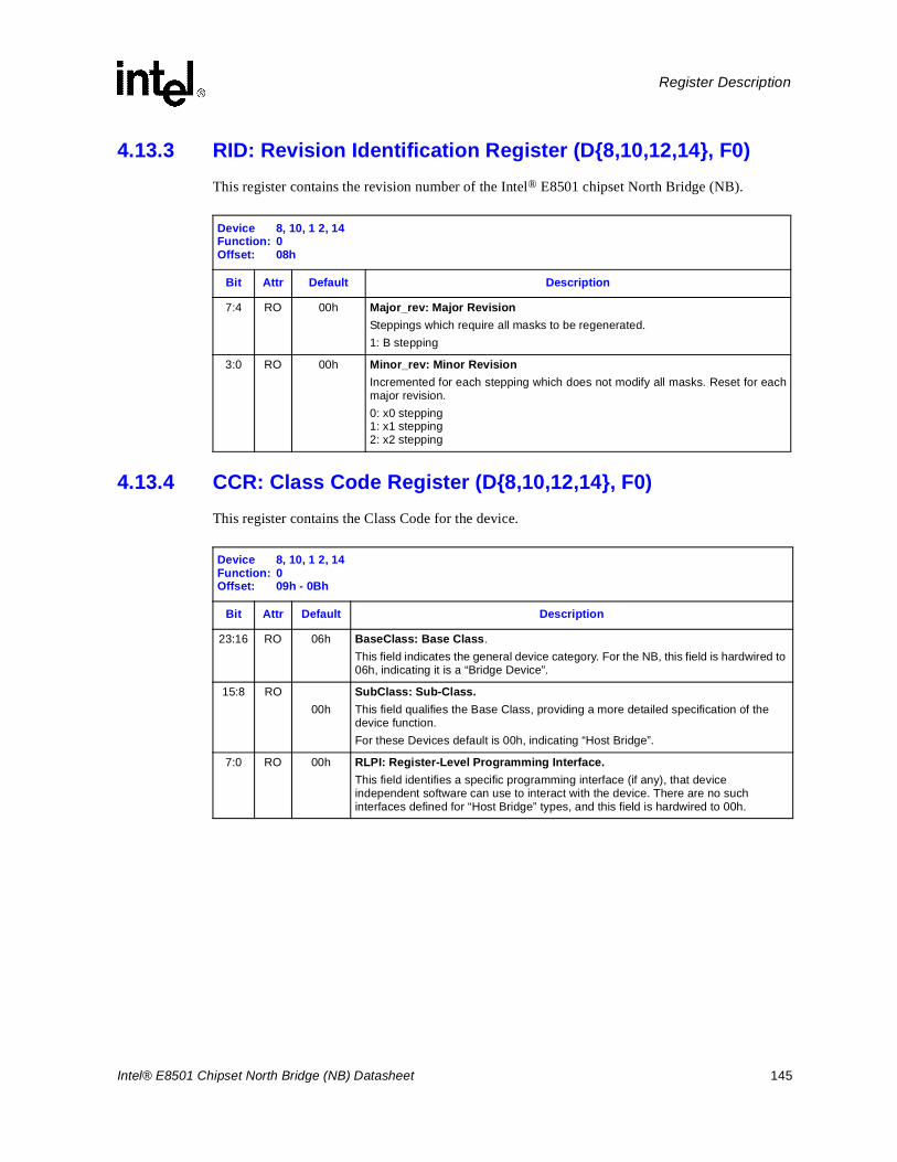
Intel® E8501 Chipset North Bridge (NB) Datasheet 145
Register Description
4.13.3 RID: Revision Identification Register (D{8,10,12,14}, F0)This register contains the revision number of the Intel® E8501 chipset North Bridge (NB).
4.13.4 CCR: Class Code Register (D{8,10,12,14}, F0)This register contains the Class Code for the device.
Device 8, 10, 1 2, 14Function: 0Offset: 08h
Bit Attr Default Description
7:4 RO 00h Major_rev: Major RevisionSteppings which require all masks to be regenerated.1: B stepping
3:0 RO 00h Minor_rev: Minor RevisionIncremented for each stepping which does not modify all masks. Reset for eachmajor revision.0: x0 stepping1: x1 stepping2: x2 stepping
Device 8, 10, 1 2, 14Function: 0Offset: 09h - 0Bh
Bit Attr Default Description
23:16 RO 06h BaseClass: Base Class.This field indicates the general device category. For the NB, this field is hardwired to 06h, indicating it is a “Bridge Device”.
15:8 RO00h
SubClass: Sub-Class.This field qualifies the Base Class, providing a more detailed specification of the device function. For these Devices default is 00h, indicating “Host Bridge”.
7:0 RO 00h RLPI: Register-Level Programming Interface.This field identifies a specific programming interface (if any), that device independent software can use to interact with the device. There are no such interfaces defined for “Host Bridge” types, and this field is hardwired to 00h.
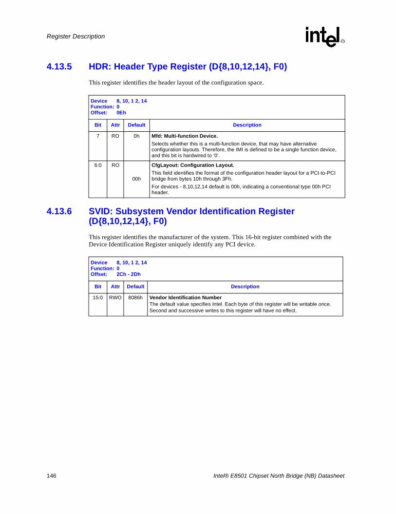
146 Intel® E8501 Chipset North Bridge (NB) Datasheet
Register Description
4.13.5 HDR: Header Type Register (D{8,10,12,14}, F0) This register identifies the header layout of the configuration space.
4.13.6 SVID: Subsystem Vendor Identification Register(D{8,10,12,14}, F0)This register identifies the manufacturer of the system. This 16-bit register combined with the Device Identification Register uniquely identify any PCI device.
Device 8, 10, 1 2, 14Function: 0Offset: 0Eh
Bit Attr Default Description
7 RO 0h Mfd: Multi-function Device.Selects whether this is a multi-function device, that may have alternative configuration layouts. Therefore, the IMI is defined to be a single function device, and this bit is hardwired to ‘0’.
6:0 RO
00h
CfgLayout: Configuration Layout.This field identifies the format of the configuration header layout for a PCI-to-PCI bridge from bytes 10h through 3Fh. For devices - 8,10,12,14 default is 00h, indicating a conventional type 00h PCI header.
Device 8, 10, 1 2, 14Function: 0Offset: 2Ch - 2Dh
Bit Attr Default Description
15:0 RWO 8086h Vendor Identification NumberThe default value specifies Intel. Each byte of this register will be writable once. Second and successive writes to this register will have no effect.
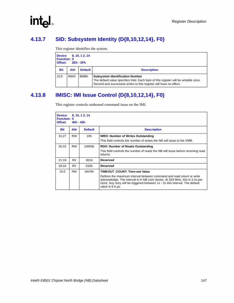
Intel® E8501 Chipset North Bridge (NB) Datasheet 147
Register Description
4.13.7 SID: Subsystem Identity (D{8,10,12,14}, F0)This register identifies the system.
4.13.8 IMISC: IMI Issue Control (D{8,10,12,14}, F0)This register controls outbound command issue on the IMI.
Device 8, 10, 1 2, 14Function: 0Offset: 2Eh - 2Fh
Bit Attr Default Description
15:0 RWO 8086h Subsystem Identification NumberThe default value specifies Intel. Each byte of this register will be writable once. Second and successive writes to this register will have no effect.
Device: 8, 10, 1 2, 14Function: 0Offset: 40h - 43h
Bit Attr Default Description
31:27 RW 10h WRO: Number of Writes OutstandingThis field controls the number of writes the NB will issue to the XMB.
26:22 RW 10000b RDO: Number of Reads OutstandingThis field controls the number of reads the NB will issue before receiving read returns.
21:19 RV 001b Reserved
18:16 RV 010b Reserved
15:0 RW 0AF0h TIMEOUT_COUNT: Time-out ValueDefines the maximum interval between command and read return or write acknowledge. The interval is in NB core clocks. At 333 MHz, this is 3 ns per clock. Any retry will be triggered between 1x - 2x this interval. The default value is 8.4 µs.
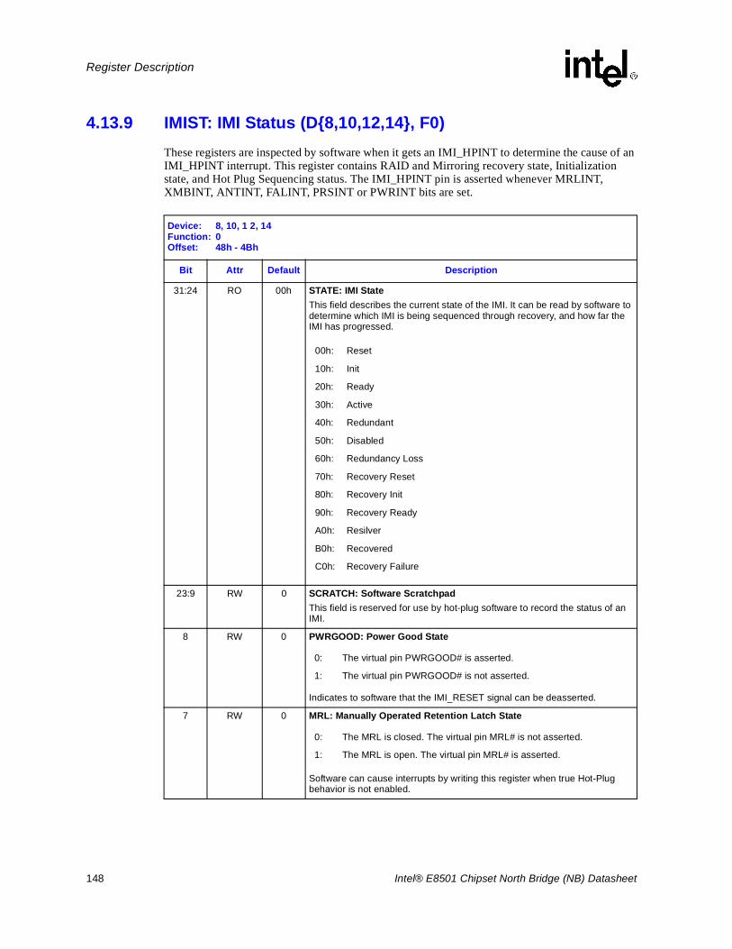
148 Intel® E8501 Chipset North Bridge (NB) Datasheet
Register Description
4.13.9 IMIST: IMI Status (D{8,10,12,14}, F0)These registers are inspected by software when it gets an IMI_HPINT to determine the cause of an IMI_HPINT interrupt. This register contains RAID and Mirroring recovery state, Initialization state, and Hot Plug Sequencing status. The IMI_HPINT pin is asserted whenever MRLINT, XMBINT, ANTINT, FALINT, PRSINT or PWRINT bits are set.
Device: 8, 10, 1 2, 14Function: 0Offset: 48h - 4Bh
Bit Attr Default Description
31:24 RO 00h STATE: IMI State This field describes the current state of the IMI. It can be read by software to determine which IMI is being sequenced through recovery, and how far the IMI has progressed.
23:9 RW 0 SCRATCH: Software Scratchpad This field is reserved for use by hot-plug software to record the status of an IMI.
8 RW 0 PWRGOOD: Power Good State
Indicates to software that the IMI_RESET signal can be deasserted.
7 RW 0 MRL: Manually Operated Retention Latch State
Software can cause interrupts by writing this register when true Hot-Plug behavior is not enabled.
00h: Reset
10h: Init
20h: Ready
30h: Active
40h: Redundant
50h: Disabled
60h: Redundancy Loss
70h: Recovery Reset
80h: Recovery Init
90h: Recovery Ready
A0h: Resilver
B0h: Recovered
C0h: Recovery Failure
0: The virtual pin PWRGOOD# is asserted.
1: The virtual pin PWRGOOD# is not asserted.
0: The MRL is closed. The virtual pin MRL# is not asserted.
1: The MRL is open. The virtual pin MRL# is asserted.
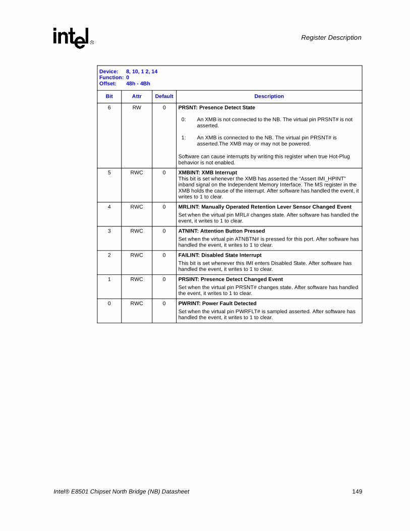
Intel® E8501 Chipset North Bridge (NB) Datasheet 149
Register Description
6 RW 0 PRSNT: Presence Detect State
Software can cause interrupts by writing this register when true Hot-Plug behavior is not enabled.
5 RWC 0 XMBINT: XMB Interrupt This bit is set whenever the XMB has asserted the “Assert IMI_HPINT” inband signal on the Independent Memory Interface. The MS register in the XMB holds the cause of the interrupt. After software has handled the event, it writes to 1 to clear.
4 RWC 0 MRLINT: Manually Operated Retention Lever Sensor Changed EventSet when the virtual pin MRL# changes state. After software has handled the event, it writes to 1 to clear.
3 RWC 0 ATNINT: Attention Button PressedSet when the virtual pin ATNBTN# is pressed for this port. After software has handled the event, it writes to 1 to clear.
2 RWC 0 FAILINT: Disabled State InterruptThis bit is set whenever this IMI enters Disabled State. After software has handled the event, it writes to 1 to clear.
1 RWC 0 PRSINT: Presence Detect Changed EventSet when the virtual pin PRSNT# changes state. After software has handled the event, it writes to 1 to clear.
0 RWC 0 PWRINT: Power Fault DetectedSet when the virtual pin PWRFLT# is sampled asserted. After software has handled the event, it writes to 1 to clear.
Device: 8, 10, 1 2, 14Function: 0Offset: 48h - 4Bh
Bit Attr Default Description
0: An XMB is not connected to the NB. The virtual pin PRSNT# is not asserted.
1: An XMB is connected to the NB. The virtual pin PRSNT# is asserted.The XMB may or may not be powered.
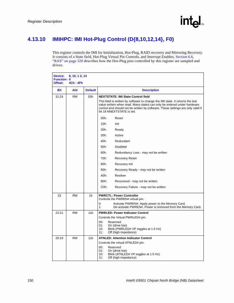
150 Intel® E8501 Chipset North Bridge (NB) Datasheet
Register Description
4.13.10 IMIHPC: IMI Hot-Plug Control (D{8,10,12,14}, F0)
This register controls the IMI for Initialization, Hot-Plug, RAID recovery and Mirroring Recovery. It consists of a State field, Hot-Plug Virtual Pin Controls, and Interrupt Enables. Section 6.6, “RAS” on page 320 describes how the Hot-Plug pins controlled by this register are sampled and driven.
Device: 8, 10, 1 2, 14Function: 0Offset: 4Ch - 4Fh
Bit Attr Default Description
31:24 RW 00h NEXTSTATE: IMI State Control fieldThis field is written by software to change the IMI state. It returns the last value written when read. Many states can only be entered under hardware control and should not be written by software. These settings are only valid if bit 18 NNEXTSTATE is set.
23 RW 1b PWRCTL: Power Controller Controls the PWREN# virtual pin.0: Activate PWREN#. Apply power to the Memory Card.1: De-activate PWREN#. Power is removed from the Memory Card.
22:21 RW 11b PWRLED: Power Indicator ControlControls the Virtual PWRLED# pin.00: Reserved01: On (drive low)10: Blink (PWRLED# VP toggles at 1.5 Hz)11: Off (high impedance)
20:19 RW 11b ATNLED: Attention Indicator ControlControls the virtual ATNLED# pin.00: Reserved01: On (drive low)10: Blink (ATNLED# VP toggles at 1.5 Hz)11: Off (high impedance)
00h: Reset
10h: Init
20h: Ready
30h: Active
40h: Redundant
50h: Disabled
60h: Redundancy Loss - may not be written
70h: Recovery Reset
80h: Recovery Init
90h: Recovery Ready - may not be written
A0h: Resilver
B0h: Recovered - may not be written
C0h: Recovery Failure - may not be written
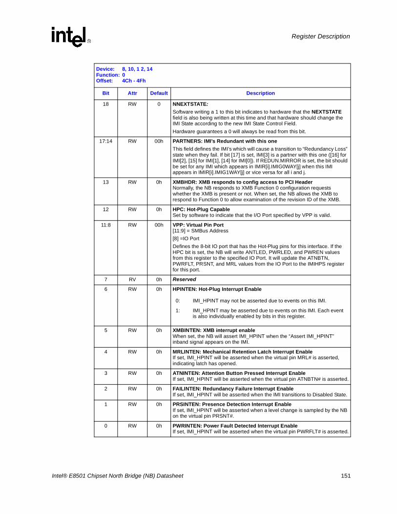
Intel® E8501 Chipset North Bridge (NB) Datasheet 151
Register Description
18 RW 0 NNEXTSTATE:Software writing a 1 to this bit indicates to hardware that the NEXTSTATEfield is also being written at this time and that hardware should change the IMI State according to the new IMI State Control Field.Hardware guarantees a 0 will always be read from this bit.
17:14 RW 00h PARTNERS: IMI’s Redundant with this one This field defines the IMI’s which will cause a transition to “Redundancy Loss” state when they fail. If bit [17] is set, IMI[3] is a partner with this one ([16] for IMI[2], [15] for IMI[1], [14] for IMI[0]). If REDUN.MIRROR is set, the bit should be set for any IMI which appears in IMIR[i].IMIG0WAY[j] when this IMI appears in IMIR[i].IMIG1WAY[j] or vice versa for all i and j.
13 RW 0h XMBHDR: XMB responds to config access to PCI Header Normally, the NB responds to XMB Function 0 configuration requests whether the XMB is present or not. When set, the NB allows the XMB to respond to Function 0 to allow examination of the revision ID of the XMB.
12 RW 0h HPC: Hot-Plug Capable Set by software to indicate that the I/O Port specified by VPP is valid.
11:8 RW 00h VPP: Virtual Pin Port [11:9] = SMBus Address[8] =IO PortDefines the 8-bit IO port that has the Hot-Plug pins for this interface. If the HPC bit is set, the NB will write ANTLED, PWRLED, and PWREN values from this register to the specified IO Port. It will update the ATNBTN, PWRFLT, PRSNT, and MRL values from the IO Port to the IMIHPS register for this port.
7 RV 0h Reserved
6 RW 0h HPINTEN: Hot-Plug Interrupt Enable
5 RW 0h XMBINTEN: XMB interrupt enable When set, the NB will assert IMI_HPINT when the “Assert IMI_HPINT” inband signal appears on the IMI.
4 RW 0h MRLINTEN: Mechanical Retention Latch Interrupt Enable If set, IMI_HPINT will be asserted when the virtual pin MRL# is asserted, indicating latch has opened.
3 RW 0h ATNINTEN: Attention Button Pressed Interrupt Enable If set, IMI_HPINT will be asserted when the virtual pin ATNBTN# is asserted.
2 RW 0h FAILINTEN: Redundancy Failure Interrupt EnableIf set, IMI_HPINT will be asserted when the IMI transitions to Disabled State.
1 RW 0h PRSINTEN: Presence Detection Interrupt Enable If set, IMI_HPINT will be asserted when a level change is sampled by the NB on the virtual pin PRSNT#.
0 RW 0h PWRINTEN: Power Fault Detected Interrupt Enable If set, IMI_HPINT will be asserted when the virtual pin PWRFLT# is asserted.
Device: 8, 10, 1 2, 14Function: 0Offset: 4Ch - 4Fh
Bit Attr Default Description
0: IMI_HPINT may not be asserted due to events on this IMI.
1: IMI_HPINT may be asserted due to events on this IMI. Each event is also individually enabled by bits in this register.
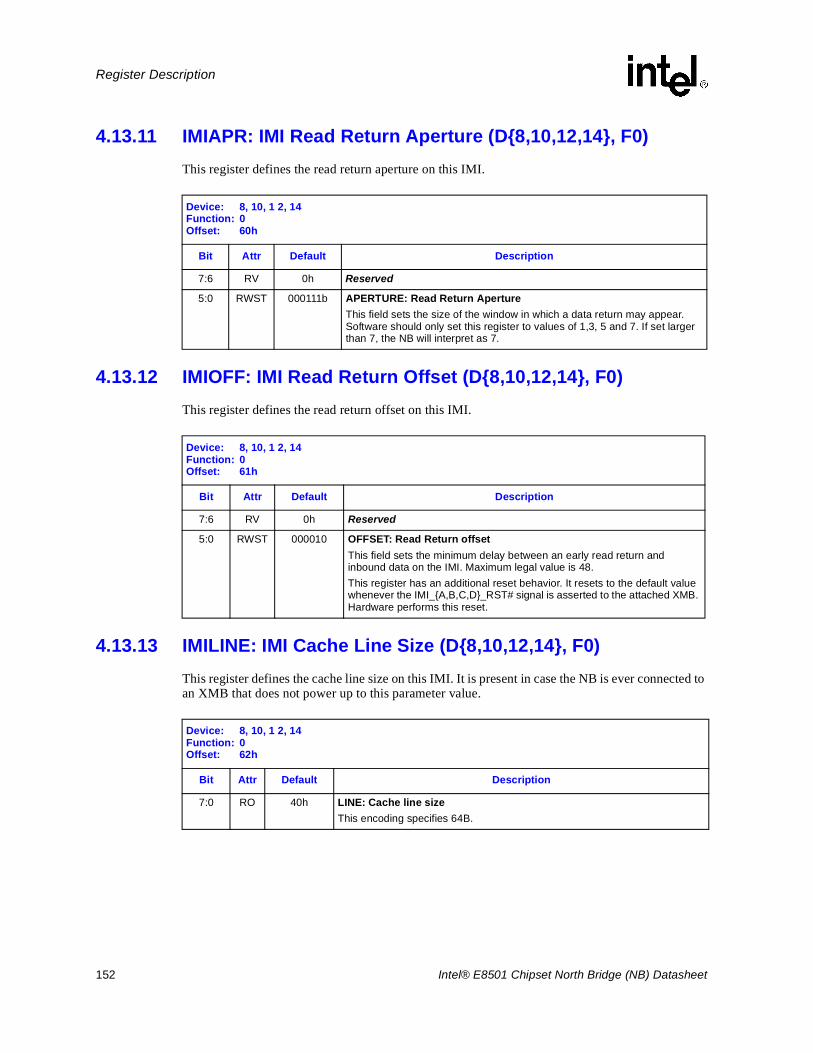
152 Intel® E8501 Chipset North Bridge (NB) Datasheet
Register Description
4.13.11 IMIAPR: IMI Read Return Aperture (D{8,10,12,14}, F0)This register defines the read return aperture on this IMI.
4.13.12 IMIOFF: IMI Read Return Offset (D{8,10,12,14}, F0)This register defines the read return offset on this IMI.
4.13.13 IMILINE: IMI Cache Line Size (D{8,10,12,14}, F0)This register defines the cache line size on this IMI. It is present in case the NB is ever connected to an XMB that does not power up to this parameter value.
Device: 8, 10, 1 2, 14Function: 0Offset: 60h
Bit Attr Default Description
7:6 RV 0h Reserved
5:0 RWST 000111b APERTURE: Read Return ApertureThis field sets the size of the window in which a data return may appear. Software should only set this register to values of 1,3, 5 and 7. If set larger than 7, the NB will interpret as 7.
Device: 8, 10, 1 2, 14Function: 0Offset: 61h
Bit Attr Default Description
7:6 RV 0h Reserved
5:0 RWST 000010 OFFSET: Read Return offsetThis field sets the minimum delay between an early read return and inbound data on the IMI. Maximum legal value is 48.This register has an additional reset behavior. It resets to the default value whenever the IMI_{A,B,C,D}_RST# signal is asserted to the attached XMB. Hardware performs this reset.
Device: 8, 10, 1 2, 14Function: 0Offset: 62h
Bit Attr Default Description
7:0 RO 40h LINE: Cache line sizeThis encoding specifies 64B.
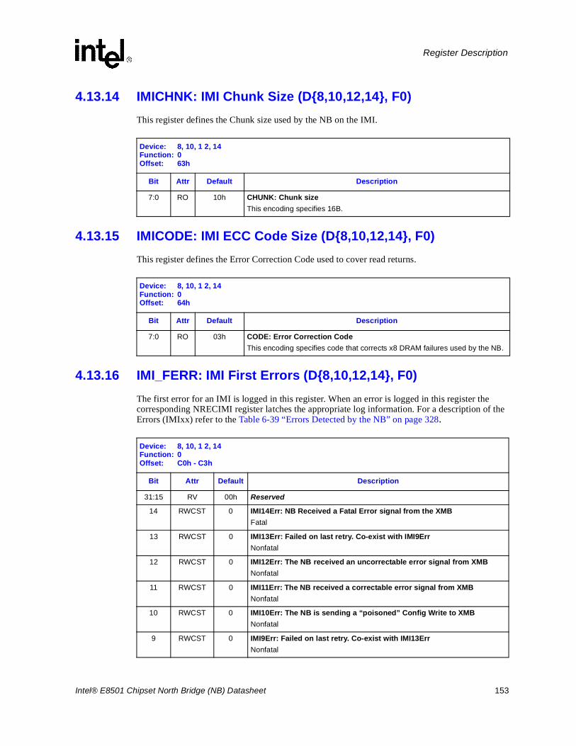
Intel® E8501 Chipset North Bridge (NB) Datasheet 153
Register Description
4.13.14 IMICHNK: IMI Chunk Size (D{8,10,12,14}, F0)This register defines the Chunk size used by the NB on the IMI.
4.13.15 IMICODE: IMI ECC Code Size (D{8,10,12,14}, F0)This register defines the Error Correction Code used to cover read returns.
4.13.16 IMI_FERR: IMI First Errors (D{8,10,12,14}, F0)The first error for an IMI is logged in this register. When an error is logged in this register the corresponding NRECIMI register latches the appropriate log information. For a description of the Errors (IMIxx) refer to the Table 6-39 “Errors Detected by the NB” on page 328.
Device: 8, 10, 1 2, 14Function: 0Offset: 63h
Bit Attr Default Description
7:0 RO 10h CHUNK: Chunk sizeThis encoding specifies 16B.
Device: 8, 10, 1 2, 14Function: 0Offset: 64h
Bit Attr Default Description
7:0 RO 03h CODE: Error Correction CodeThis encoding specifies code that corrects x8 DRAM failures used by the NB.
Device: 8, 10, 1 2, 14Function: 0Offset: C0h - C3h
Bit Attr Default Description
31:15 RV 00h Reserved
14 RWCST 0 IMI14Err: NB Received a Fatal Error signal from the XMBFatal
13 RWCST 0 IMI13Err: Failed on last retry. Co-exist with IMI9ErrNonfatal
12 RWCST 0 IMI12Err: The NB received an uncorrectable error signal from XMBNonfatal
11 RWCST 0 IMI11Err: The NB received a correctable error signal from XMBNonfatal
10 RWCST 0 IMI10Err: The NB is sending a “poisoned” Config Write to XMBNonfatal
9 RWCST 0 IMI9Err: Failed on last retry. Co-exist with IMI13ErrNonfatal
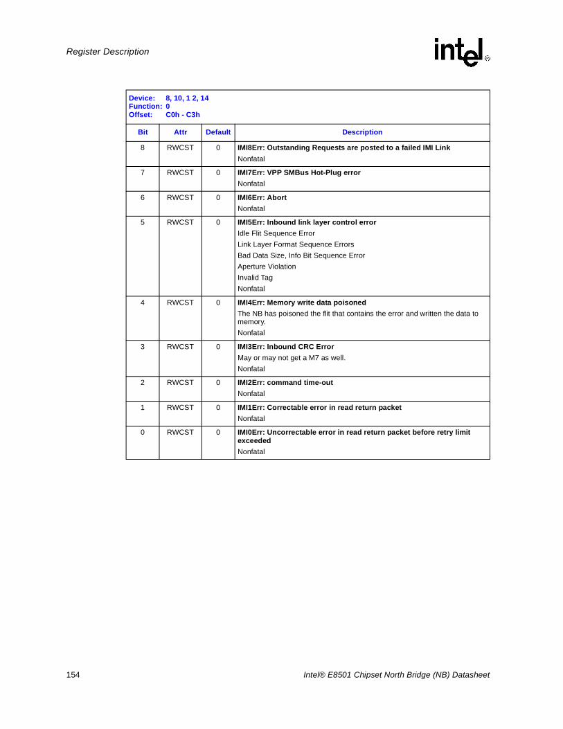
154 Intel® E8501 Chipset North Bridge (NB) Datasheet
Register Description
8 RWCST 0 IMI8Err: Outstanding Requests are posted to a failed IMI LinkNonfatal
7 RWCST 0 IMI7Err: VPP SMBus Hot-Plug errorNonfatal
6 RWCST 0 IMI6Err: AbortNonfatal
5 RWCST 0 IMI5Err: Inbound link layer control errorIdle Flit Sequence ErrorLink Layer Format Sequence ErrorsBad Data Size, Info Bit Sequence ErrorAperture ViolationInvalid TagNonfatal
4 RWCST 0 IMI4Err: Memory write data poisonedThe NB has poisoned the flit that contains the error and written the data to memory. Nonfatal
3 RWCST 0 IMI3Err: Inbound CRC ErrorMay or may not get a M7 as well.Nonfatal
2 RWCST 0 IMI2Err: command time-outNonfatal
1 RWCST 0 IMI1Err: Correctable error in read return packetNonfatal
0 RWCST 0 IMI0Err: Uncorrectable error in read return packet before retry limit exceeded Nonfatal
Device: 8, 10, 1 2, 14Function: 0Offset: C0h - C3h
Bit Attr Default Description
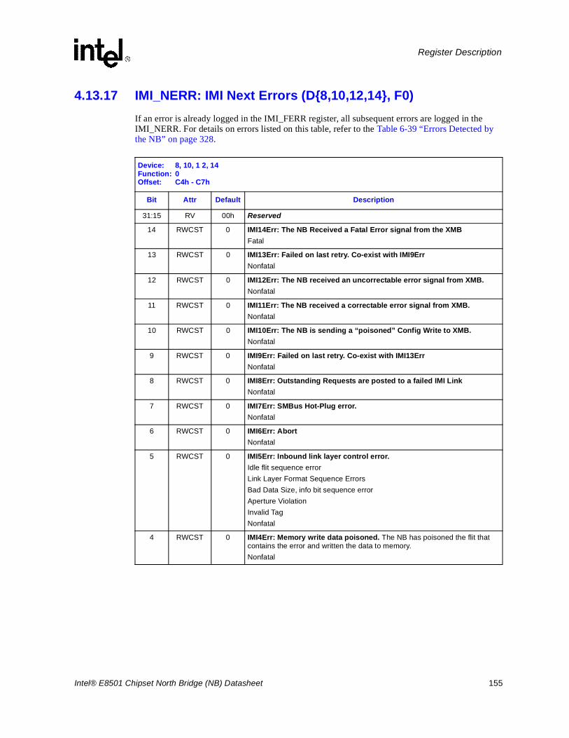
Intel® E8501 Chipset North Bridge (NB) Datasheet 155
Register Description
4.13.17 IMI_NERR: IMI Next Errors (D{8,10,12,14}, F0)If an error is already logged in the IMI_FERR register, all subsequent errors are logged in the IMI_NERR. For details on errors listed on this table, refer to the Table 6-39 “Errors Detected by the NB” on page 328.
Device: 8, 10, 1 2, 14Function: 0Offset: C4h - C7h
Bit Attr Default Description
31:15 RV 00h Reserved
14 RWCST 0 IMI14Err: The NB Received a Fatal Error signal from the XMBFatal
13 RWCST 0 IMI13Err: Failed on last retry. Co-exist with IMI9ErrNonfatal
12 RWCST 0 IMI12Err: The NB received an uncorrectable error signal from XMB. Nonfatal
11 RWCST 0 IMI11Err: The NB received a correctable error signal from XMB.Nonfatal
10 RWCST 0 IMI10Err: The NB is sending a “poisoned” Config Write to XMB.Nonfatal
9 RWCST 0 IMI9Err: Failed on last retry. Co-exist with IMI13ErrNonfatal
8 RWCST 0 IMI8Err: Outstanding Requests are posted to a failed IMI LinkNonfatal
7 RWCST 0 IMI7Err: SMBus Hot-Plug error.Nonfatal
6 RWCST 0 IMI6Err: AbortNonfatal
5 RWCST 0 IMI5Err: Inbound link layer control error.Idle flit sequence errorLink Layer Format Sequence ErrorsBad Data Size, info bit sequence errorAperture ViolationInvalid TagNonfatal
4 RWCST 0 IMI4Err: Memory write data poisoned. The NB has poisoned the flit that contains the error and written the data to memory. Nonfatal
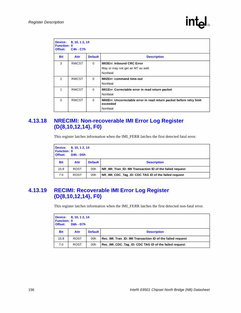
156 Intel® E8501 Chipset North Bridge (NB) Datasheet
Register Description
4.13.18 NRECIMI: Non-recoverable IMI Error Log Register(D{8,10,12,14}, F0)This register latches information when the IMI_FERR latches the first detected fatal error.
4.13.19 RECIMI: Recoverable IMI Error Log Register(D{8,10,12,14}, F0)This register latches information when the IMI_FERR latches the first detected non-fatal error.
3 RWCST 0 IMI3Err: Inbound CRC ErrorMay or may not get an M7 as well.Nonfatal
2 RWCST 0 IMI2Err: command time-outNonfatal
1 RWCST 0 IMI1Err: Correctable error in read return packetNonfatal
0 RWCST 0 IMI0Err: Uncorrectable error in read return packet before retry limit exceeded Nonfatal
Device: 8, 10, 1 2, 14Function: 0Offset: C4h - C7h
Bit Attr Default Description
Device: 8, 10, 1 2, 14Function: 0Offset: D4h - D5h
Bit Attr Default Description
15:8 ROST 00h NR_IMI_Tran_ID: IMI Transaction ID of the failed request
7:0 ROST 00h NR_IMI_CDC_Tag_ID: CDC TAG ID of the failed request
Device: 8, 10, 1 2, 14Function: 0Offset: D6h - D7h
Bit Attr Default Description
15:8 ROST 00h Rec_IMI_Tran_ID: IMI Transaction ID of the failed request
7:0 ROST 00h Rec_IMI_CDC_Tag_ID: CDC TAG ID of the failed request
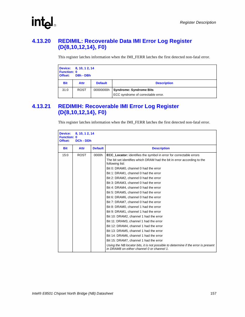
Intel® E8501 Chipset North Bridge (NB) Datasheet 157
Register Description
4.13.20 REDIMIL: Recoverable Data IMI Error Log Register(D{8,10,12,14}, F0)This register latches information when the IMI_FERR latches the first detected non-fatal error.
4.13.21 REDIMIH: Recoverable IMI Error Log Register (D{8,10,12,14}, F0)This register latches information when the IMI_FERR latches the first detected non-fatal error.
Device: 8, 10, 1 2, 14Function: 0Offset: D8h - DBh
Bit Attr Default Description
31:0 ROST 00000000h Syndrome: Syndrome BitsECC syndrome of correctable error.
Device: 8, 10, 1 2, 14Function: 0Offset: DCh - DDh
Bit Attr Default Description
15:0 ROST 0000h ECC_Locator: identifies the symbol in error for correctable errorsThe bit set identifies which DRAM had the bit in error according to the following list:Bit 0: DRAM0, channel 0 had the errorBit 1: DRAM1, channel 0 had the errorBit 2: DRAM2, channel 0 had the errorBit 3: DRAM3, channel 0 had the errorBit 4: DRAM4, channel 0 had the errorBit 5: DRAM5, channel 0 had the errorBit 6: DRAM6, channel 0 had the errorBit 7: DRAM7, channel 0 had the errorBit 8: DRAM0, channel 1 had the errorBit 9: DRAM1, channel 1 had the errorBit 10: DRAM2, channel 1 had the errorBit 11: DRAM3, channel 1 had the errorBit 12: DRAM4, channel 1 had the errorBit 13: DRAM5, channel 1 had the errorBit 14: DRAM6, channel 1 had the errorBit 15: DRAM7, channel 1 had the errorUsing the NB locator bits, it is not possible to determine if the error is present in DRAM8 on either channel 0 or channel 1.
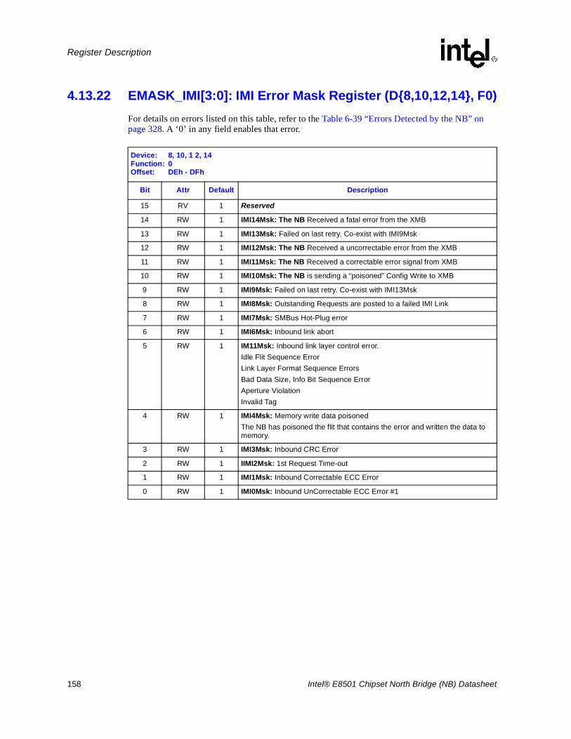
158 Intel® E8501 Chipset North Bridge (NB) Datasheet
Register Description
4.13.22 EMASK_IMI[3:0]: IMI Error Mask Register (D{8,10,12,14}, F0)For details on errors listed on this table, refer to the Table 6-39 “Errors Detected by the NB” on page 328. A ‘0’ in any field enables that error.
Device: 8, 10, 1 2, 14Function: 0Offset: DEh - DFh
Bit Attr Default Description
15 RV 1 Reserved
14 RW 1 IMI14Msk: The NB Received a fatal error from the XMB
13 RW 1 IMI13Msk: Failed on last retry. Co-exist with IMI9Msk
12 RW 1 IMI12Msk: The NB Received a uncorrectable error from the XMB
11 RW 1 IMI11Msk: The NB Received a correctable error signal from XMB
10 RW 1 IMI10Msk: The NB is sending a “poisoned” Config Write to XMB
9 RW 1 IMI9Msk: Failed on last retry. Co-exist with IMI13Msk
8 RW 1 IMI8Msk: Outstanding Requests are posted to a failed IMI Link
7 RW 1 IMI7Msk: SMBus Hot-Plug error
6 RW 1 IMI6Msk: Inbound link abort
5 RW 1 IM11Msk: Inbound link layer control error.Idle Flit Sequence ErrorLink Layer Format Sequence ErrorsBad Data Size, Info Bit Sequence ErrorAperture ViolationInvalid Tag
4 RW 1 IMI4Msk: Memory write data poisonedThe NB has poisoned the flit that contains the error and written the data to memory.
3 RW 1 IMI3Msk: Inbound CRC Error
2 RW 1 IIMI2Msk: 1st Request Time-out
1 RW 1 IMI1Msk: Inbound Correctable ECC Error
0 RW 1 IMI0Msk: Inbound UnCorrectable ECC Error #1
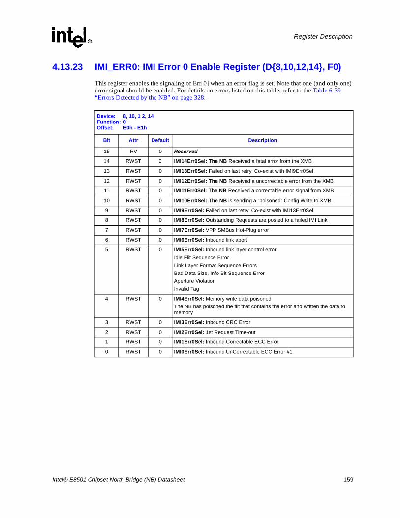
Intel® E8501 Chipset North Bridge (NB) Datasheet 159
Register Description
4.13.23 IMI_ERR0: IMI Error 0 Enable Register (D{8,10,12,14}, F0)This register enables the signaling of Err[0] when an error flag is set. Note that one (and only one) error signal should be enabled. For details on errors listed on this table, refer to the Table 6-39 “Errors Detected by the NB” on page 328.
Device: 8, 10, 1 2, 14Function: 0Offset: E0h - E1h
Bit Attr Default Description
15 RV 0 Reserved
14 RWST 0 IMI14Err0Sel: The NB Received a fatal error from the XMB
13 RWST 0 IMI13Err0Sel: Failed on last retry. Co-exist with IMI9Err0Sel
12 RWST 0 IMI12Err0Sel: The NB Received a uncorrectable error from the XMB
11 RWST 0 IMI11Err0Sel: The NB Received a correctable error signal from XMB
10 RWST 0 IMI10Err0Sel: The NB is sending a “poisoned” Config Write to XMB
9 RWST 0 IMI9Err0Sel: Failed on last retry. Co-exist with IMI13Err0Sel
8 RWST 0 IMI8Err0Sel: Outstanding Requests are posted to a failed IMI Link
7 RWST 0 IMI7Err0Sel: VPP SMBus Hot-Plug error
6 RWST 0 IMI6Err0Sel: Inbound link abort
5 RWST 0 IMI5Err0Sel: Inbound link layer control errorIdle Flit Sequence ErrorLink Layer Format Sequence ErrorsBad Data Size, Info Bit Sequence ErrorAperture ViolationInvalid Tag
4 RWST 0 IMI4Err0Sel: Memory write data poisonedThe NB has poisoned the flit that contains the error and written the data to memory
3 RWST 0 IMI3Err0Sel: Inbound CRC Error
2 RWST 0 IMI2Err0Sel: 1st Request Time-out
1 RWST 0 IMI1Err0Sel: Inbound Correctable ECC Error
0 RWST 0 IMI0Err0Sel: Inbound UnCorrectable ECC Error #1
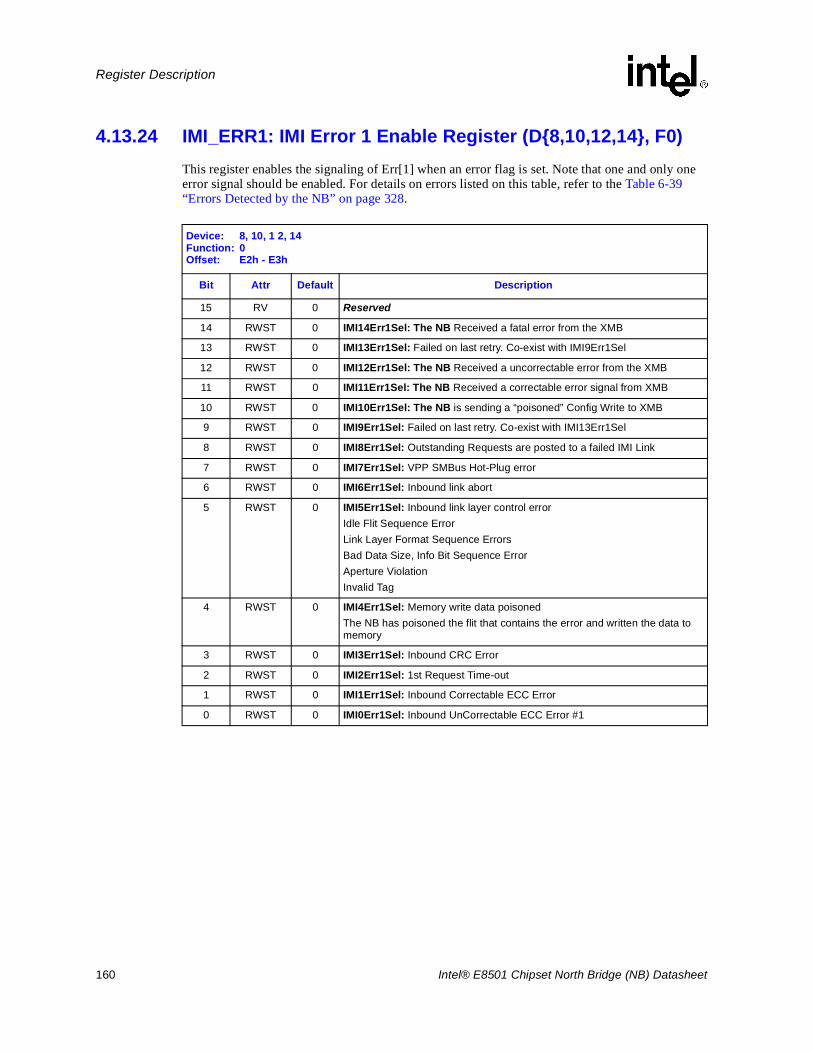
160 Intel® E8501 Chipset North Bridge (NB) Datasheet
Register Description
4.13.24 IMI_ERR1: IMI Error 1 Enable Register (D{8,10,12,14}, F0)This register enables the signaling of Err[1] when an error flag is set. Note that one and only one error signal should be enabled. For details on errors listed on this table, refer to the Table 6-39 “Errors Detected by the NB” on page 328.
Device: 8, 10, 1 2, 14Function: 0Offset: E2h - E3h
Bit Attr Default Description
15 RV 0 Reserved
14 RWST 0 IMI14Err1Sel: The NB Received a fatal error from the XMB
13 RWST 0 IMI13Err1Sel: Failed on last retry. Co-exist with IMI9Err1Sel
12 RWST 0 IMI12Err1Sel: The NB Received a uncorrectable error from the XMB
11 RWST 0 IMI11Err1Sel: The NB Received a correctable error signal from XMB
10 RWST 0 IMI10Err1Sel: The NB is sending a “poisoned” Config Write to XMB
9 RWST 0 IMI9Err1Sel: Failed on last retry. Co-exist with IMI13Err1Sel
8 RWST 0 IMI8Err1Sel: Outstanding Requests are posted to a failed IMI Link
7 RWST 0 IMI7Err1Sel: VPP SMBus Hot-Plug error
6 RWST 0 IMI6Err1Sel: Inbound link abort
5 RWST 0 IMI5Err1Sel: Inbound link layer control errorIdle Flit Sequence ErrorLink Layer Format Sequence ErrorsBad Data Size, Info Bit Sequence ErrorAperture ViolationInvalid Tag
4 RWST 0 IMI4Err1Sel: Memory write data poisonedThe NB has poisoned the flit that contains the error and written the data to memory
3 RWST 0 IMI3Err1Sel: Inbound CRC Error
2 RWST 0 IMI2Err1Sel: 1st Request Time-out
1 RWST 0 IMI1Err1Sel: Inbound Correctable ECC Error
0 RWST 0 IMI0Err1Sel: Inbound UnCorrectable ECC Error #1
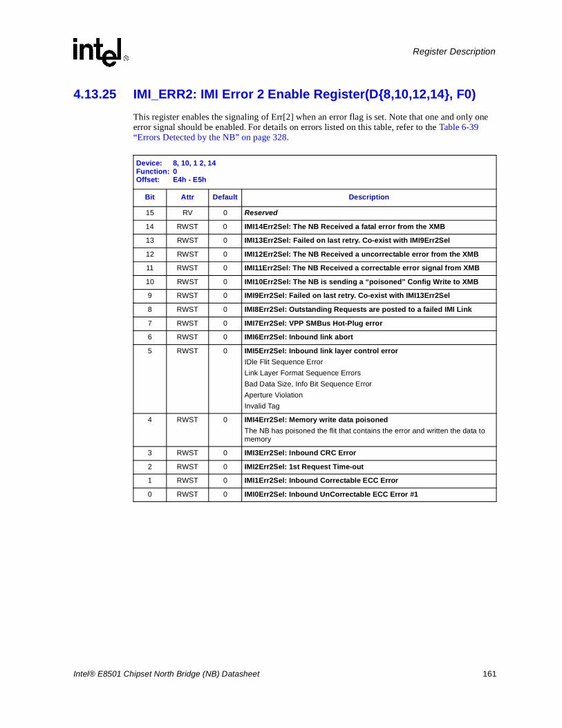
Intel® E8501 Chipset North Bridge (NB) Datasheet 161
Register Description
4.13.25 IMI_ERR2: IMI Error 2 Enable Register(D{8,10,12,14}, F0)This register enables the signaling of Err[2] when an error flag is set. Note that one and only one error signal should be enabled. For details on errors listed on this table, refer to the Table 6-39 “Errors Detected by the NB” on page 328.
Device: 8, 10, 1 2, 14Function: 0Offset: E4h - E5h
Bit Attr Default Description
15 RV 0 Reserved
14 RWST 0 IMI14Err2Sel: The NB Received a fatal error from the XMB
13 RWST 0 IMI13Err2Sel: Failed on last retry. Co-exist with IMI9Err2Sel
12 RWST 0 IMI12Err2Sel: The NB Received a uncorrectable error from the XMB
11 RWST 0 IMI11Err2Sel: The NB Received a correctable error signal from XMB
10 RWST 0 IMI10Err2Sel: The NB is sending a “poisoned” Config Write to XMB
9 RWST 0 IMI9Err2Sel: Failed on last retry. Co-exist with IMI13Err2Sel
8 RWST 0 IMI8Err2Sel: Outstanding Requests are posted to a failed IMI Link
7 RWST 0 IMI7Err2Sel: VPP SMBus Hot-Plug error
6 RWST 0 IMI6Err2Sel: Inbound link abort
5 RWST 0 IMI5Err2Sel: Inbound link layer control errorIDle Flit Sequence ErrorLink Layer Format Sequence ErrorsBad Data Size, Info Bit Sequence ErrorAperture ViolationInvalid Tag
4 RWST 0 IMI4Err2Sel: Memory write data poisonedThe NB has poisoned the flit that contains the error and written the data to memory
3 RWST 0 IMI3Err2Sel: Inbound CRC Error
2 RWST 0 IMI2Err2Sel: 1st Request Time-out
1 RWST 0 IMI1Err2Sel: Inbound Correctable ECC Error
0 RWST 0 IMI0Err2Sel: Inbound UnCorrectable ECC Error #1
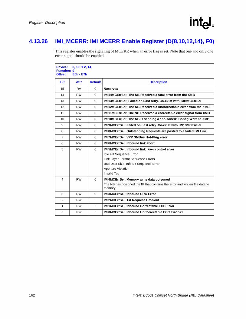
162 Intel® E8501 Chipset North Bridge (NB) Datasheet
Register Description
4.13.26 IMI_MCERR: IMI MCERR Enable Register (D{8,10,12,14}, F0)This register enables the signaling of MCERR when an error flag is set. Note that one and only one error signal should be enabled.
Device: 8, 10, 1 2, 14Function: 0Offset: E6h - E7h
Bit Attr Default Description
15 RV 0 Reserved
14 RW 0 IMI14MCErrSel: The NB Received a fatal error from the XMB
13 RW 0 IMI13MCErrSel: Failed on Last retry. Co-exist with IMI9MCErrSel
12 RW 0 IMI12MCErrSel: The NB Received a uncorrectable error from the XMB
11 RW 0 IMI11MCErrSel: The NB Received a correctable error signal from XMB
10 RW 0 IMI10MCErrSel: The NB is sending a “poisoned” Config Write to XMB
9 RW 0 IMI9MCErrSel: Failed on Last retry. Co-exist with IMI13MCErrSel
8 RW 0 IMI8MCErrSel: Outstanding Requests are posted to a failed IMI Link
7 RW 0 IMI7MCErrSel: VPP SMBus Hot-Plug error
6 RW 0 IMI6MCErrSel: Inbound link abort
5 RW 0 IMI5MCErrSel: Inbound link layer control errorIdle Flit Sequence ErrorLink Layer Format Sequence ErrorsBad Data Size, Info Bit Sequence ErrorAperture ViolationInvalid Tag
4 RW 0 IMI4MCErrSel: Memory write data poisonedThe NB has poisoned the flit that contains the error and written the data to memory
3 RW 0 IMI3MCErrSel: Inbound CRC Error
2 RW 0 IMI2MCErrSel: 1st Request Time-out
1 RW 0 IMI1MCErrSel: Inbound Correctable ECC Error
0 RW 0 IMI0MCErrSel: Inbound UnCorrectable ECC Error #1
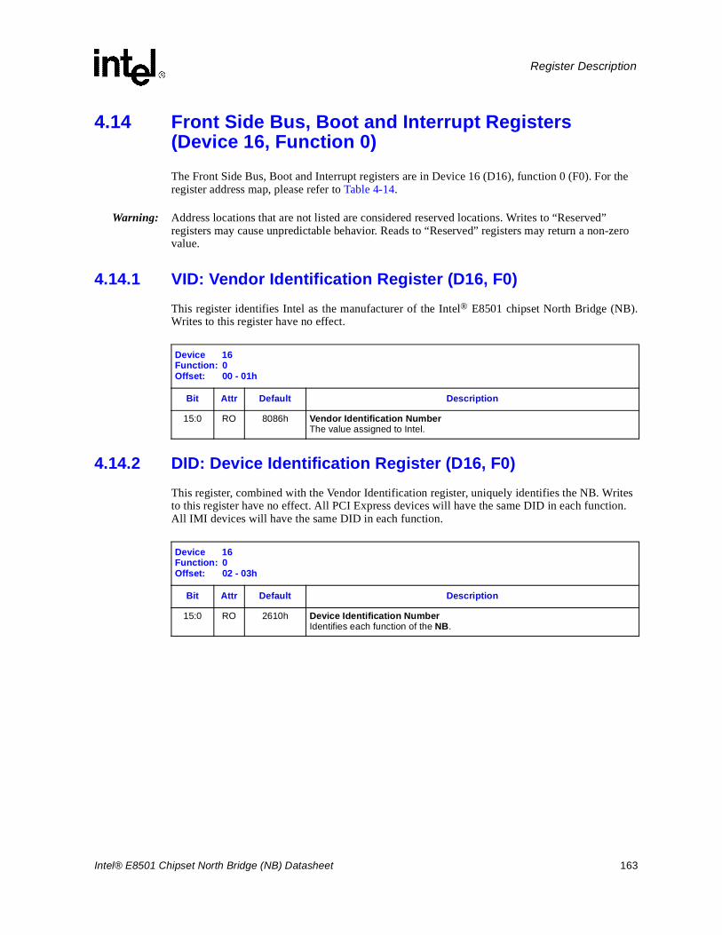
Intel® E8501 Chipset North Bridge (NB) Datasheet 163
Register Description
4.14 Front Side Bus, Boot and Interrupt Registers(Device 16, Function 0)The Front Side Bus, Boot and Interrupt registers are in Device 16 (D16), function 0 (F0). For the register address map, please refer to Table 4-14.
Warning: Address locations that are not listed are considered reserved locations. Writes to “Reserved” registers may cause unpredictable behavior. Reads to “Reserved” registers may return a non-zero value.
4.14.1 VID: Vendor Identification Register (D16, F0)This register identifies Intel as the manufacturer of the Intel® E8501 chipset North Bridge (NB).Writes to this register have no effect.
4.14.2 DID: Device Identification Register (D16, F0)This register, combined with the Vendor Identification register, uniquely identifies the NB. Writes to this register have no effect. All PCI Express devices will have the same DID in each function. All IMI devices will have the same DID in each function.
Device 16Function: 0Offset: 00 - 01h
Bit Attr Default Description
15:0 RO 8086h Vendor Identification NumberThe value assigned to Intel.
Device 16Function: 0Offset: 02 - 03h
Bit Attr Default Description
15:0 RO 2610h Device Identification Number Identifies each function of the NB.
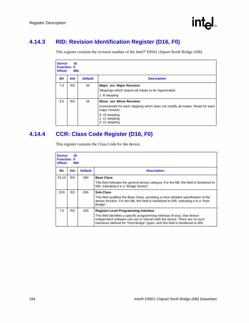
164 Intel® E8501 Chipset North Bridge (NB) Datasheet
Register Description
4.14.3 RID: Revision Identification Register (D16, F0)This register contains the revision number of the Intel® E8501 chipset North Bridge (NB).
.
4.14.4 CCR: Class Code Register (D16, F0)This register contains the Class Code for the device.
Device 16Function: 0Offset: 08h
Bit Attr Default Description
7:4 RO 0h Major_rev: Major RevisionSteppings which require all masks to be regenerated.1: B stepping
3:0 RO 0h Minor_rev: Minor RevisionIncremented for each stepping which does not modify all masks. Reset for eachmajor revision.0: x0 stepping1: x1 stepping2: x2 stepping
Device 16Function: 0Offset: 09h
Bit Attr Default Description
23:16 RO 06h Base ClassThis field indicates the general device category. For the NB, this field is hardwired to 06h, indicating it is a “Bridge Device”.
15:8 RO 00h Sub-ClassThis field qualifies the Base Class, providing a more detailed specification of the device function. For the NB, this field is hardwired to 00h, indicating it is a “Host Bridge”.
7:0 RO 00h Register-Level Programming InterfaceThis field identifies a specific programming interface (if any), that device-independent software can use to interact with the device. There are no such interfaces defined for “Host Bridge” types, and this field is hardwired to 00h.
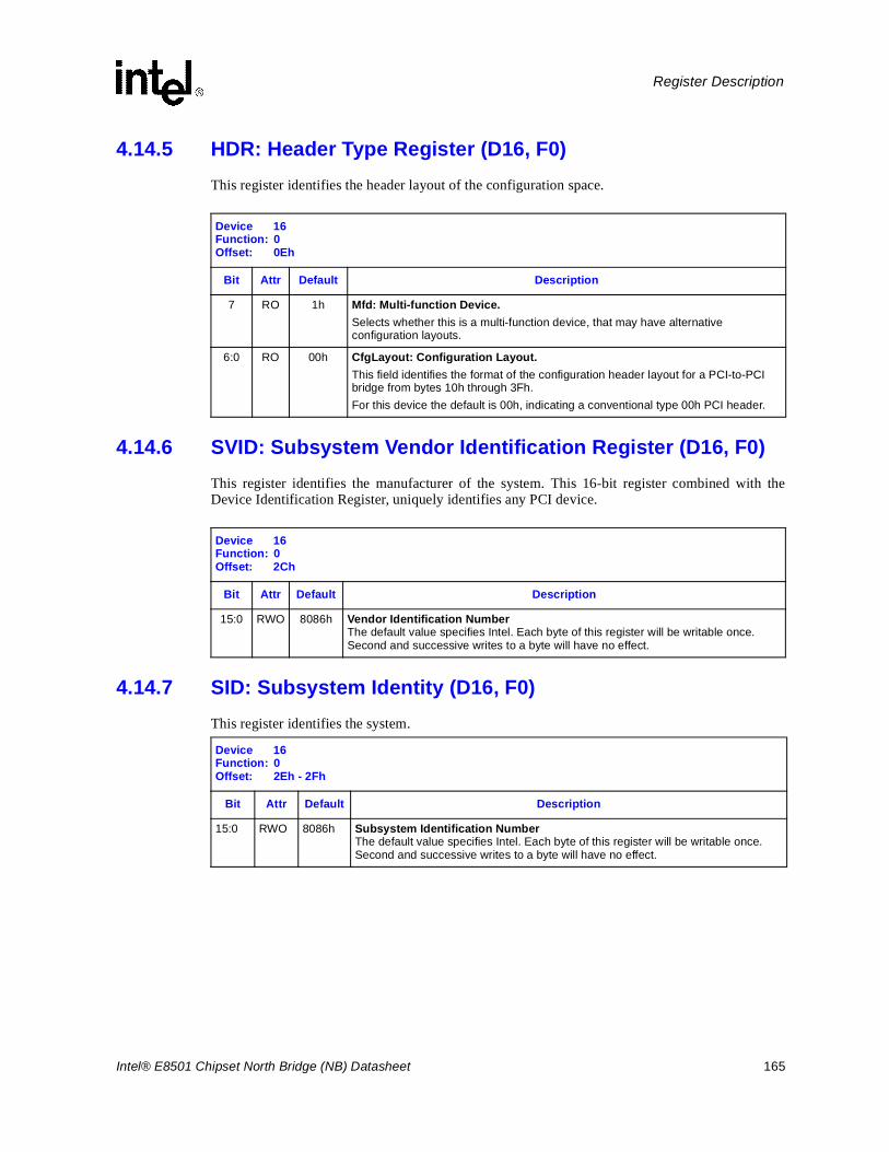
Intel® E8501 Chipset North Bridge (NB) Datasheet 165
Register Description
4.14.5 HDR: Header Type Register (D16, F0)This register identifies the header layout of the configuration space.
4.14.6 SVID: Subsystem Vendor Identification Register (D16, F0)This register identifies the manufacturer of the system. This 16-bit register combined with theDevice Identification Register, uniquely identifies any PCI device.
4.14.7 SID: Subsystem Identity (D16, F0)This register identifies the system.
Device 16Function: 0Offset: 0Eh
Bit Attr Default Description
7 RO 1h Mfd: Multi-function Device.Selects whether this is a multi-function device, that may have alternative configuration layouts.
6:0 RO 00h CfgLayout: Configuration Layout.This field identifies the format of the configuration header layout for a PCI-to-PCI bridge from bytes 10h through 3Fh. For this device the default is 00h, indicating a conventional type 00h PCI header.
Device 16Function: 0Offset: 2Ch
Bit Attr Default Description
15:0 RWO 8086h Vendor Identification NumberThe default value specifies Intel. Each byte of this register will be writable once. Second and successive writes to a byte will have no effect.
Device 16Function: 0Offset: 2Eh - 2Fh
Bit Attr Default Description
15:0 RWO 8086h Subsystem Identification Number The default value specifies Intel. Each byte of this register will be writable once. Second and successive writes to a byte will have no effect.
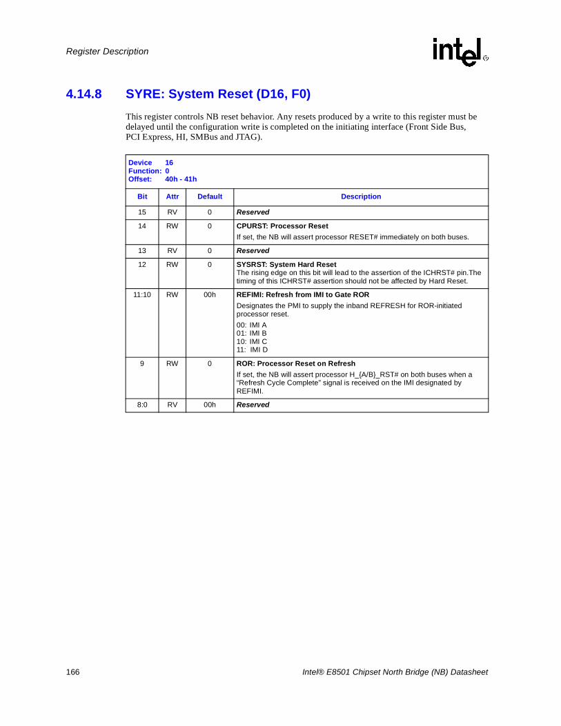
166 Intel® E8501 Chipset North Bridge (NB) Datasheet
Register Description
4.14.8 SYRE: System Reset (D16, F0)This register controls NB reset behavior. Any resets produced by a write to this register must be delayed until the configuration write is completed on the initiating interface (Front Side Bus, PCI Express, HI, SMBus and JTAG).
Device 16Function: 0Offset: 40h - 41h
Bit Attr Default Description
15 RV 0 Reserved
14 RW 0 CPURST: Processor ResetIf set, the NB will assert processor RESET# immediately on both buses.
13 RV 0 Reserved
12 RW 0 SYSRST: System Hard ResetThe rising edge on this bit will lead to the assertion of the ICHRST# pin.The timing of this ICHRST# assertion should not be affected by Hard Reset.
11:10 RW 00h REFIMI: Refresh from IMI to Gate RORDesignates the PMI to supply the inband REFRESH for ROR-initiated processor reset.00: IMI A01: IMI B10: IMI C11: IMI D
9 RW 0 ROR: Processor Reset on RefreshIf set, the NB will assert processor H_{A/B}_RST# on both buses when a “Refresh Cycle Complete” signal is received on the IMI designated by REFIMI.
8:0 RV 00h Reserved
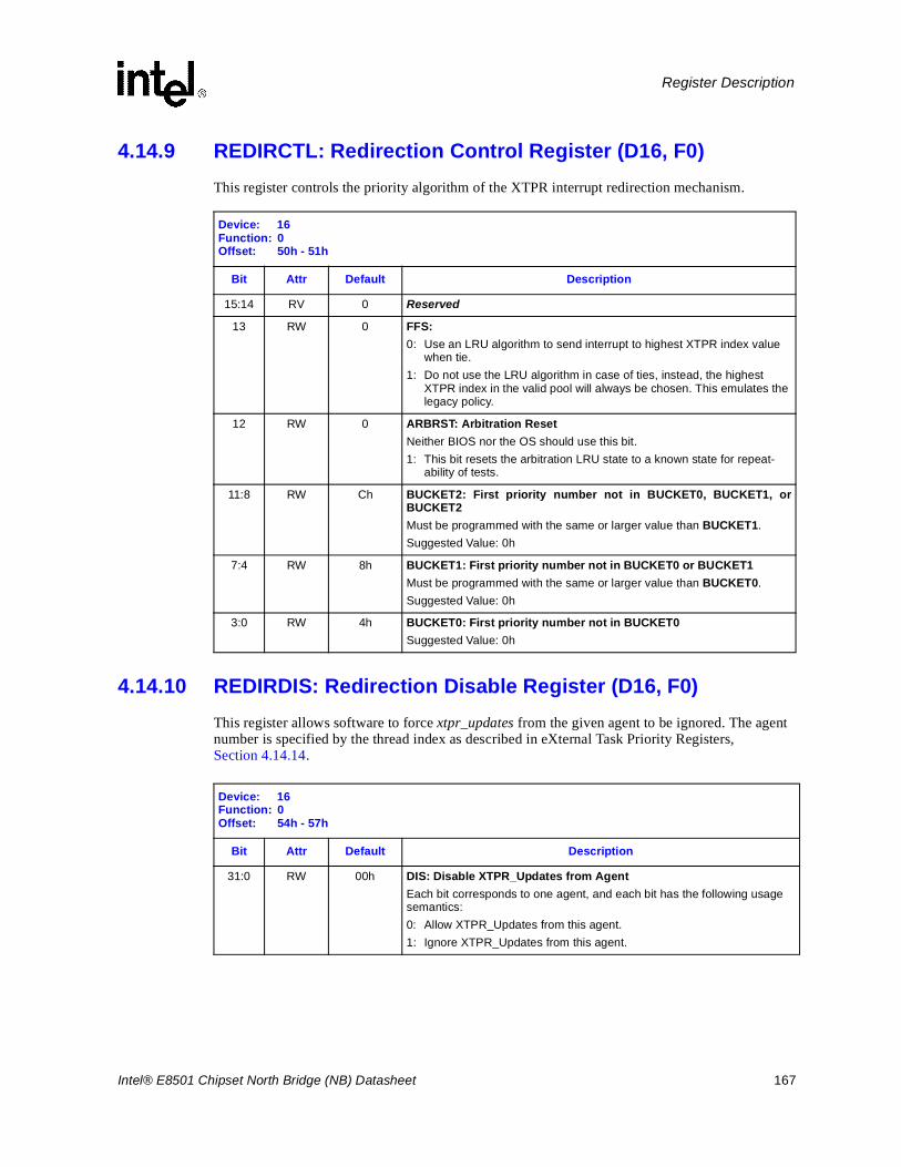
Intel® E8501 Chipset North Bridge (NB) Datasheet 167
Register Description
4.14.9 REDIRCTL: Redirection Control Register (D16, F0)This register controls the priority algorithm of the XTPR interrupt redirection mechanism.
4.14.10 REDIRDIS: Redirection Disable Register (D16, F0)This register allows software to force xtpr_updates from the given agent to be ignored. The agent number is specified by the thread index as described in eXternal Task Priority Registers, Section 4.14.14.
Device: 16Function: 0Offset: 50h - 51h
Bit Attr Default Description
15:14 RV 0 Reserved
13 RW 0 FFS: 0: Use an LRU algorithm to send interrupt to highest XTPR index value
when tie.1: Do not use the LRU algorithm in case of ties, instead, the highest
XTPR index in the valid pool will always be chosen. This emulates the legacy policy.
12 RW 0 ARBRST: Arbitration ResetNeither BIOS nor the OS should use this bit.1: This bit resets the arbitration LRU state to a known state for repeat-
ability of tests.
11:8 RW Ch BUCKET2: First priority number not in BUCKET0, BUCKET1, orBUCKET2Must be programmed with the same or larger value than BUCKET1.Suggested Value: 0h
7:4 RW 8h BUCKET1: First priority number not in BUCKET0 or BUCKET1Must be programmed with the same or larger value than BUCKET0.Suggested Value: 0h
3:0 RW 4h BUCKET0: First priority number not in BUCKET0Suggested Value: 0h
Device: 16Function: 0Offset: 54h - 57h
Bit Attr Default Description
31:0 RW 00h DIS: Disable XTPR_Updates from AgentEach bit corresponds to one agent, and each bit has the following usage semantics:0: Allow XTPR_Updates from this agent.1: Ignore XTPR_Updates from this agent.
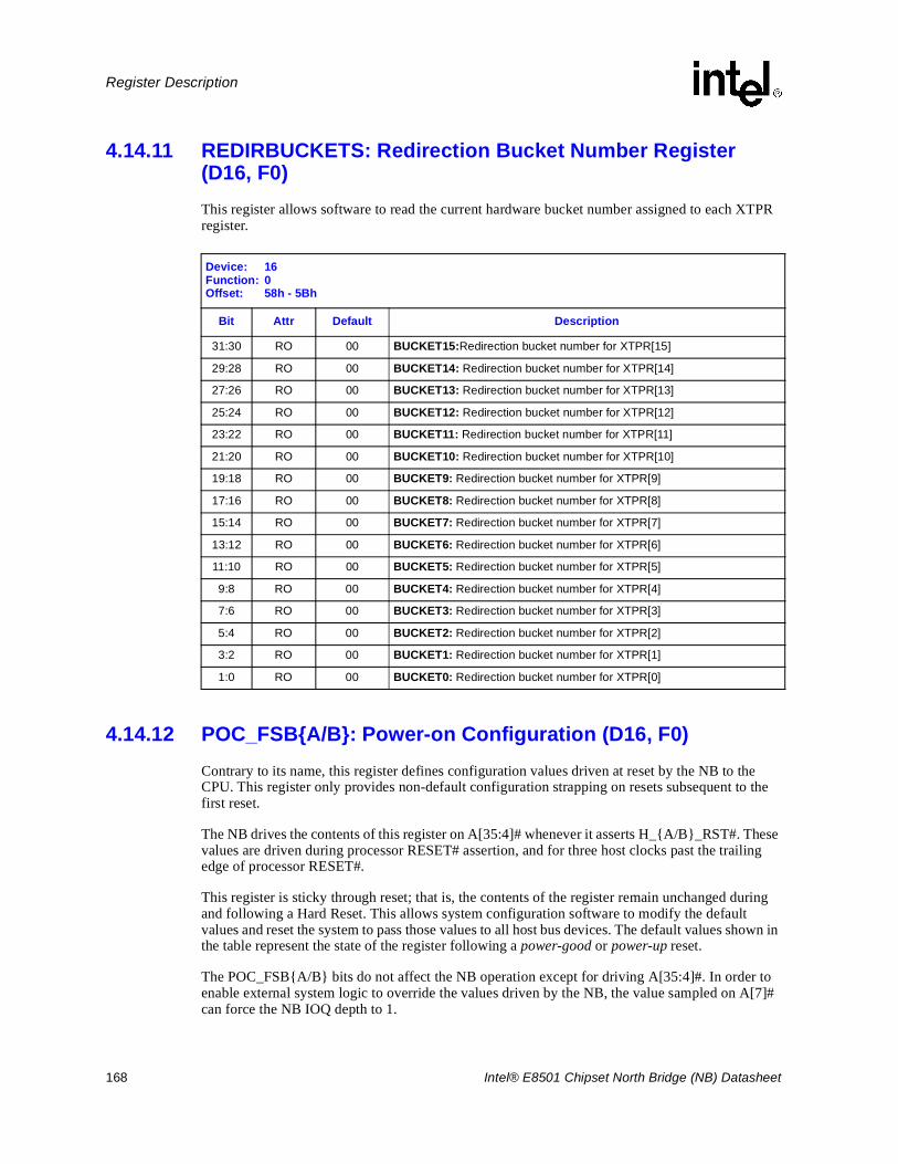
168 Intel® E8501 Chipset North Bridge (NB) Datasheet
Register Description
4.14.11 REDIRBUCKETS: Redirection Bucket Number Register (D16, F0)This register allows software to read the current hardware bucket number assigned to each XTPR register.
4.14.12 POC_FSB{A/B}: Power-on Configuration (D16, F0)Contrary to its name, this register defines configuration values driven at reset by the NB to the CPU. This register only provides non-default configuration strapping on resets subsequent to the first reset.
The NB drives the contents of this register on A[35:4]# whenever it asserts H_{A/B}_RST#. These values are driven during processor RESET# assertion, and for three host clocks past the trailing edge of processor RESET#.
This register is sticky through reset; that is, the contents of the register remain unchanged during and following a Hard Reset. This allows system configuration software to modify the default values and reset the system to pass those values to all host bus devices. The default values shown in the table represent the state of the register following a power-good or power-up reset.
The POC_FSB{A/B} bits do not affect the NB operation except for driving A[35:4]#. In order to enable external system logic to override the values driven by the NB, the value sampled on A[7]# can force the NB IOQ depth to 1.
Device: 16Function: 0Offset: 58h - 5Bh
Bit Attr Default Description
31:30 RO 00 BUCKET15:Redirection bucket number for XTPR[15]
29:28 RO 00 BUCKET14: Redirection bucket number for XTPR[14]
27:26 RO 00 BUCKET13: Redirection bucket number for XTPR[13]
25:24 RO 00 BUCKET12: Redirection bucket number for XTPR[12]
23:22 RO 00 BUCKET11: Redirection bucket number for XTPR[11]
21:20 RO 00 BUCKET10: Redirection bucket number for XTPR[10]
19:18 RO 00 BUCKET9: Redirection bucket number for XTPR[9]
17:16 RO 00 BUCKET8: Redirection bucket number for XTPR[8]
15:14 RO 00 BUCKET7: Redirection bucket number for XTPR[7]
13:12 RO 00 BUCKET6: Redirection bucket number for XTPR[6]
11:10 RO 00 BUCKET5: Redirection bucket number for XTPR[5]
9:8 RO 00 BUCKET4: Redirection bucket number for XTPR[4]
7:6 RO 00 BUCKET3: Redirection bucket number for XTPR[3]
5:4 RO 00 BUCKET2: Redirection bucket number for XTPR[2]
3:2 RO 00 BUCKET1: Redirection bucket number for XTPR[1]
1:0 RO 00 BUCKET0: Redirection bucket number for XTPR[0]
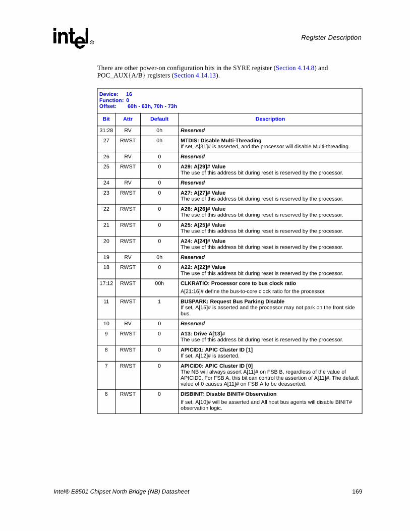
Intel® E8501 Chipset North Bridge (NB) Datasheet 169
Register Description
There are other power-on configuration bits in the SYRE register (Section 4.14.8) and POC_AUX{A/B} registers (Section 4.14.13).
Device: 16Function: 0Offset: 60h - 63h, 70h - 73h
Bit Attr Default Description
31:28 RV 0h Reserved
27 RWST 0h MTDIS: Disable Multi-ThreadingIf set, A[31]# is asserted, and the processor will disable Multi-threading.
26 RV 0 Reserved
25 RWST 0 A29: A[29]# ValueThe use of this address bit during reset is reserved by the processor.
24 RV 0 Reserved
23 RWST 0 A27: A[27]# ValueThe use of this address bit during reset is reserved by the processor.
22 RWST 0 A26: A[26]# ValueThe use of this address bit during reset is reserved by the processor.
21 RWST 0 A25: A[25]# ValueThe use of this address bit during reset is reserved by the processor.
20 RWST 0 A24: A[24]# ValueThe use of this address bit during reset is reserved by the processor.
19 RV 0h Reserved
18 RWST 0 A22: A[22]# ValueThe use of this address bit during reset is reserved by the processor.
17:12 RWST 00h CLKRATIO: Processor core to bus clock ratioA[21:16]# define the bus-to-core clock ratio for the processor.
11 RWST 1 BUSPARK: Request Bus Parking DisableIf set, A[15]# is asserted and the processor may not park on the front side bus.
10 RV 0 Reserved
9 RWST 0 A13: Drive A[13]#The use of this address bit during reset is reserved by the processor.
8 RWST 0 APICID1: APIC Cluster ID [1]If set, A[12]# is asserted.
7 RWST 0 APICID0: APIC Cluster ID [0]The NB will always assert A[11]# on FSB B, regardless of the value of APICID0. For FSB A, this bit can control the assertion of A[11]#. The default value of 0 causes A[11]# on FSB A to be deasserted.
6 RWST 0 DISBINIT: Disable BINIT# ObservationIf set, A[10]# will be asserted and All host bus agents will disable BINIT# observation logic.
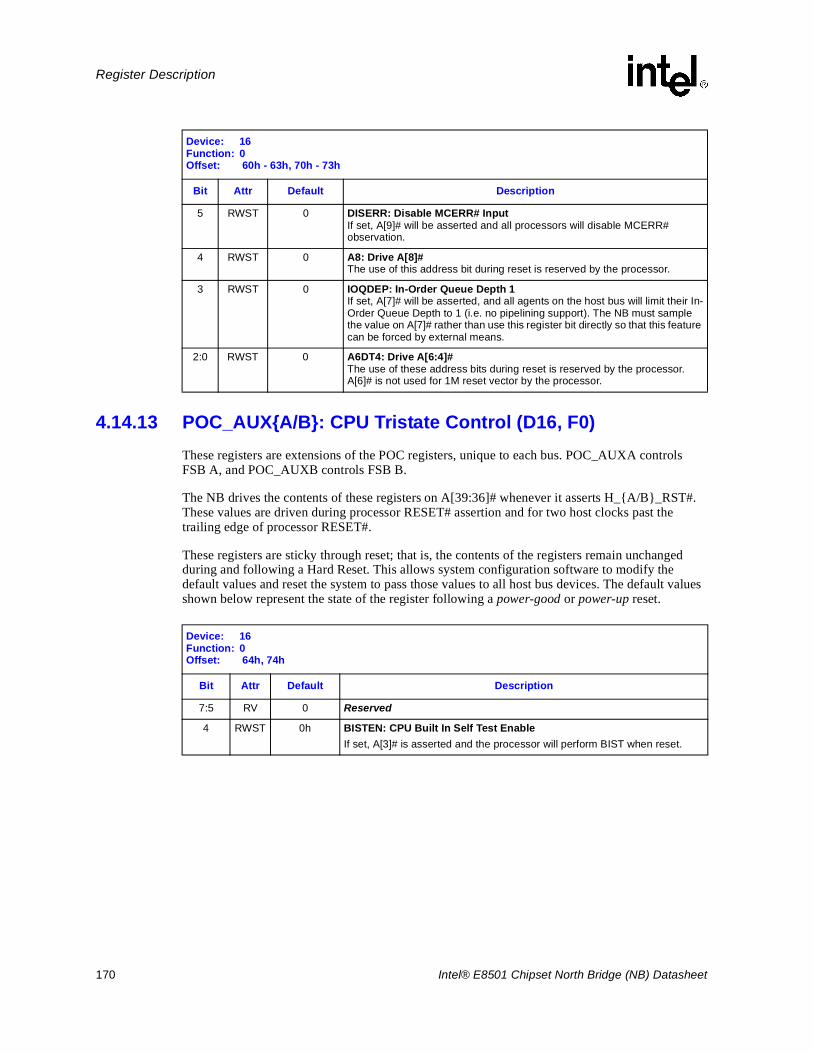
170 Intel® E8501 Chipset North Bridge (NB) Datasheet
Register Description
4.14.13 POC_AUX{A/B}: CPU Tristate Control (D16, F0)These registers are extensions of the POC registers, unique to each bus. POC_AUXA controls FSB A, and POC_AUXB controls FSB B.
The NB drives the contents of these registers on A[39:36]# whenever it asserts H_{A/B}_RST#. These values are driven during processor RESET# assertion and for two host clocks past the trailing edge of processor RESET#.
These registers are sticky through reset; that is, the contents of the registers remain unchanged during and following a Hard Reset. This allows system configuration software to modify the default values and reset the system to pass those values to all host bus devices. The default values shown below represent the state of the register following a power-good or power-up reset.
5 RWST 0 DISERR: Disable MCERR# InputIf set, A[9]# will be asserted and all processors will disable MCERR# observation.
4 RWST 0 A8: Drive A[8]#The use of this address bit during reset is reserved by the processor.
3 RWST 0 IOQDEP: In-Order Queue Depth 1If set, A[7]# will be asserted, and all agents on the host bus will limit their In-Order Queue Depth to 1 (i.e. no pipelining support). The NB must sample the value on A[7]# rather than use this register bit directly so that this feature can be forced by external means.
2:0 RWST 0 A6DT4: Drive A[6:4]# The use of these address bits during reset is reserved by the processor. A[6]# is not used for 1M reset vector by the processor.
Device: 16Function: 0Offset: 60h - 63h, 70h - 73h
Bit Attr Default Description
Device: 16Function: 0Offset: 64h, 74h
Bit Attr Default Description
7:5 RV 0 Reserved
4 RWST 0h BISTEN: CPU Built In Self Test EnableIf set, A[3]# is asserted and the processor will perform BIST when reset.
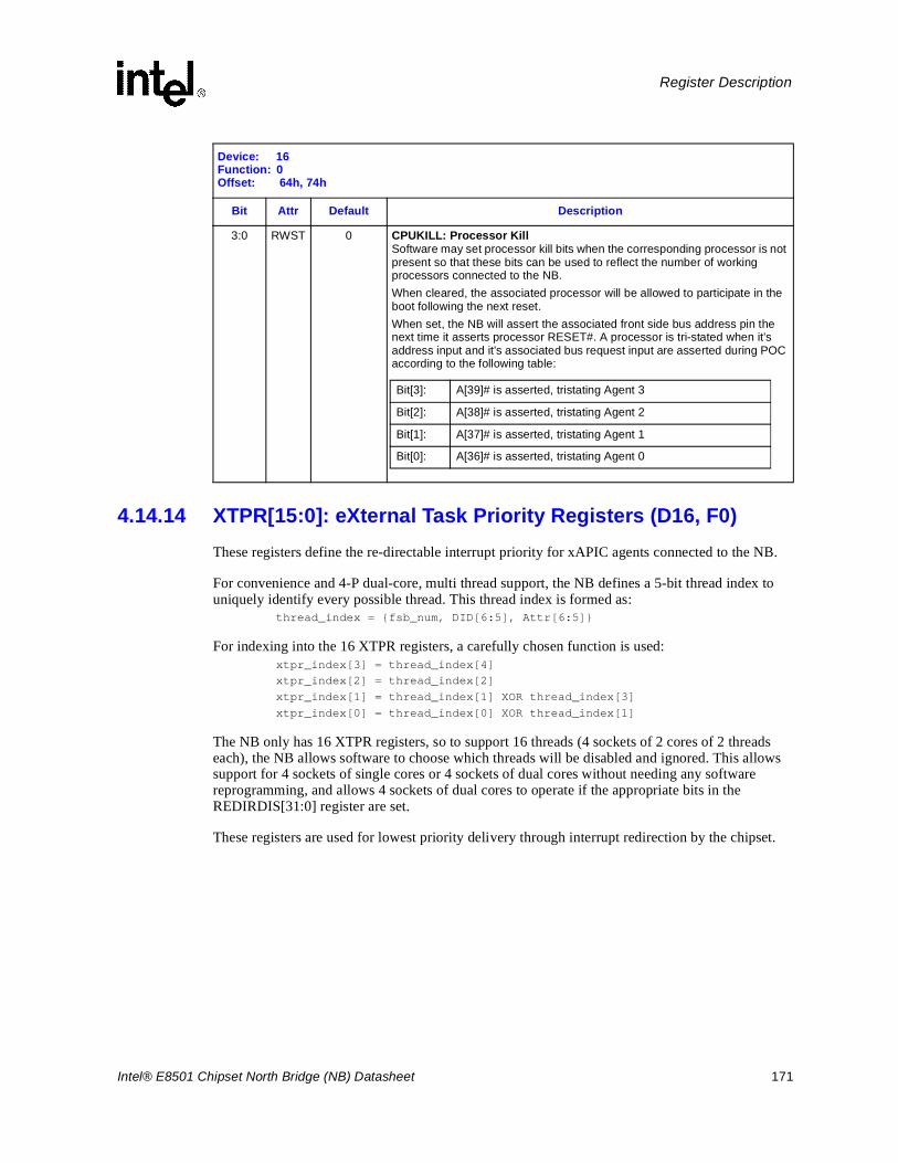
Intel® E8501 Chipset North Bridge (NB) Datasheet 171
Register Description
4.14.14 XTPR[15:0]: eXternal Task Priority Registers (D16, F0)These registers define the re-directable interrupt priority for xAPIC agents connected to the NB.
For convenience and 4-P dual-core, multi thread support, the NB defines a 5-bit thread index to uniquely identify every possible thread. This thread index is formed as:
thread_index = {fsb_num, DID[6:5], Attr[6:5]}
For indexing into the 16 XTPR registers, a carefully chosen function is used:xtpr_index[3] = thread_index[4]xtpr_index[2] = thread_index[2]xtpr_index[1] = thread_index[1] XOR thread_index[3]xtpr_index[0] = thread_index[0] XOR thread_index[1]
The NB only has 16 XTPR registers, so to support 16 threads (4 sockets of 2 cores of 2 threads each), the NB allows software to choose which threads will be disabled and ignored. This allows support for 4 sockets of single cores or 4 sockets of dual cores without needing any software reprogramming, and allows 4 sockets of dual cores to operate if the appropriate bits in the REDIRDIS[31:0] register are set.
These registers are used for lowest priority delivery through interrupt redirection by the chipset.
3:0 RWST 0 CPUKILL: Processor KillSoftware may set processor kill bits when the corresponding processor is not present so that these bits can be used to reflect the number of working processors connected to the NB.When cleared, the associated processor will be allowed to participate in the boot following the next reset. When set, the NB will assert the associated front side bus address pin the next time it asserts processor RESET#. A processor is tri-stated when it’s address input and it’s associated bus request input are asserted during POC according to the following table:
Device: 16Function: 0Offset: 64h, 74h
Bit Attr Default Description
Bit[3]: A[39]# is asserted, tristating Agent 3
Bit[2]: A[38]# is asserted, tristating Agent 2
Bit[1]: A[37]# is asserted, tristating Agent 1
Bit[0]: A[36]# is asserted, tristating Agent 0
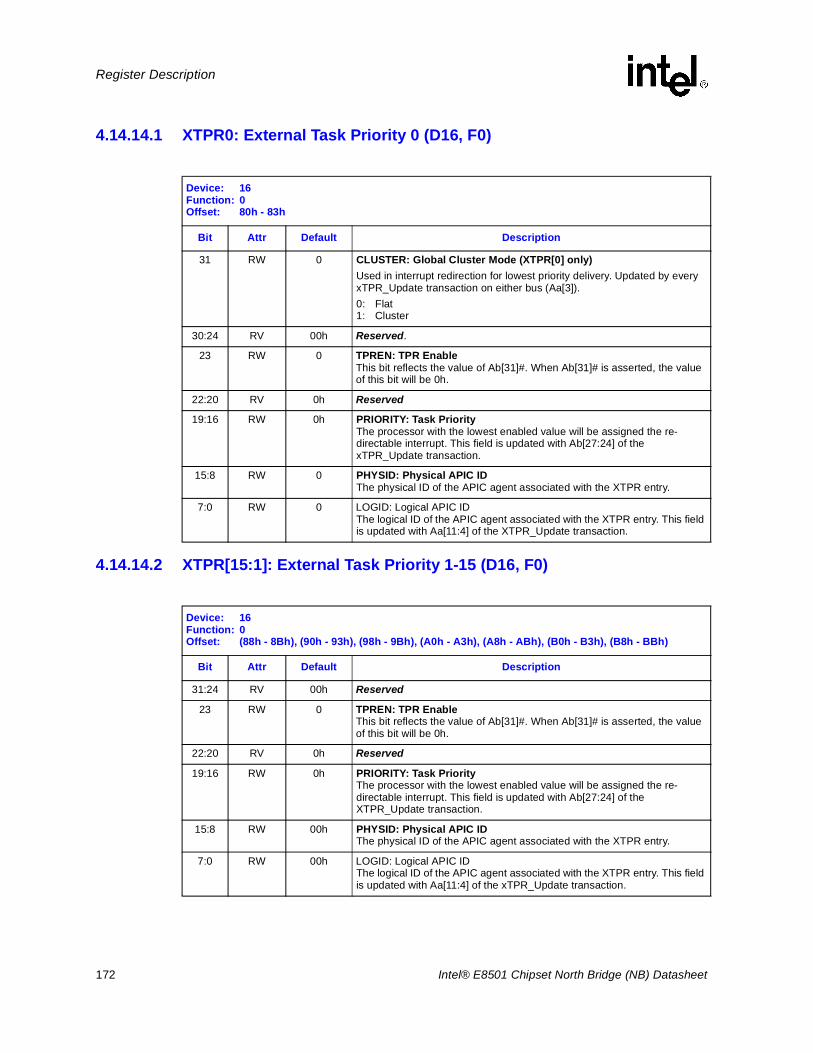
172 Intel® E8501 Chipset North Bridge (NB) Datasheet
Register Description
4.14.14.1 XTPR0: External Task Priority 0 (D16, F0)
4.14.14.2 XTPR[15:1]: External Task Priority 1-15 (D16, F0)
Device: 16Function: 0Offset: 80h - 83h
Bit Attr Default Description
31 RW 0 CLUSTER: Global Cluster Mode (XTPR[0] only)Used in interrupt redirection for lowest priority delivery. Updated by every xTPR_Update transaction on either bus (Aa[3]). 0: Flat1: Cluster
30:24 RV 00h Reserved.
23 RW 0 TPREN: TPR EnableThis bit reflects the value of Ab[31]#. When Ab[31]# is asserted, the value of this bit will be 0h.
22:20 RV 0h Reserved
19:16 RW 0h PRIORITY: Task PriorityThe processor with the lowest enabled value will be assigned the re-directable interrupt. This field is updated with Ab[27:24] of the xTPR_Update transaction.
15:8 RW 0 PHYSID: Physical APIC IDThe physical ID of the APIC agent associated with the XTPR entry.
7:0 RW 0 LOGID: Logical APIC IDThe logical ID of the APIC agent associated with the XTPR entry. This field is updated with Aa[11:4] of the XTPR_Update transaction.
Device: 16Function: 0Offset: (88h - 8Bh), (90h - 93h), (98h - 9Bh), (A0h - A3h), (A8h - ABh), (B0h - B3h), (B8h - BBh)
Bit Attr Default Description
31:24 RV 00h Reserved
23 RW 0 TPREN: TPR EnableThis bit reflects the value of Ab[31]#. When Ab[31]# is asserted, the value of this bit will be 0h.
22:20 RV 0h Reserved
19:16 RW 0h PRIORITY: Task PriorityThe processor with the lowest enabled value will be assigned the re-directable interrupt. This field is updated with Ab[27:24] of the XTPR_Update transaction.
15:8 RW 00h PHYSID: Physical APIC IDThe physical ID of the APIC agent associated with the XTPR entry.
7:0 RW 00h LOGID: Logical APIC IDThe logical ID of the APIC agent associated with the XTPR entry. This field is updated with Aa[11:4] of the xTPR_Update transaction.
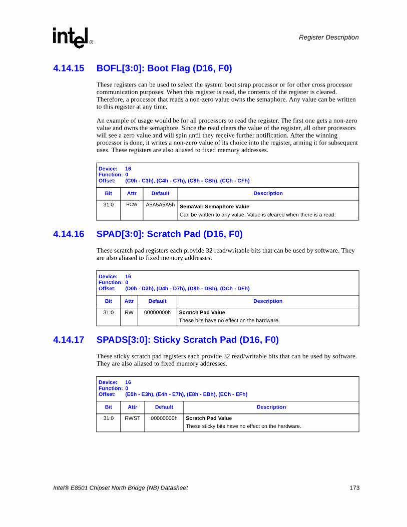
Intel® E8501 Chipset North Bridge (NB) Datasheet 173
Register Description
4.14.15 BOFL[3:0]: Boot Flag (D16, F0)These registers can be used to select the system boot strap processor or for other cross processor communication purposes. When this register is read, the contents of the register is cleared. Therefore, a processor that reads a non-zero value owns the semaphore. Any value can be written to this register at any time.
An example of usage would be for all processors to read the register. The first one gets a non-zero value and owns the semaphore. Since the read clears the value of the register, all other processors will see a zero value and will spin until they receive further notification. After the winning processor is done, it writes a non-zero value of its choice into the register, arming it for subsequent uses. These registers are also aliased to fixed memory addresses.
4.14.16 SPAD[3:0]: Scratch Pad (D16, F0)These scratch pad registers each provide 32 read/writable bits that can be used by software. They are also aliased to fixed memory addresses.
4.14.17 SPADS[3:0]: Sticky Scratch Pad (D16, F0)These sticky scratch pad registers each provide 32 read/writable bits that can be used by software. They are also aliased to fixed memory addresses.
Device: 16Function: 0Offset: (C0h - C3h), (C4h - C7h), (C8h - CBh), (CCh - CFh)
Bit Attr Default Description
31:0 RCW A5A5A5A5h SemaVal: Semaphore ValueCan be written to any value. Value is cleared when there is a read.
Device: 16Function: 0Offset: (D0h - D3h), (D4h - D7h), (D8h - DBh), (DCh - DFh)
Bit Attr Default Description
31:0 RW 00000000h Scratch Pad ValueThese bits have no effect on the hardware.
Device: 16Function: 0Offset: (E0h - E3h), (E4h - E7h), (E8h - EBh), (ECh - EFh)
Bit Attr Default Description
31:0 RWST 00000000h Scratch Pad ValueThese sticky bits have no effect on the hardware.
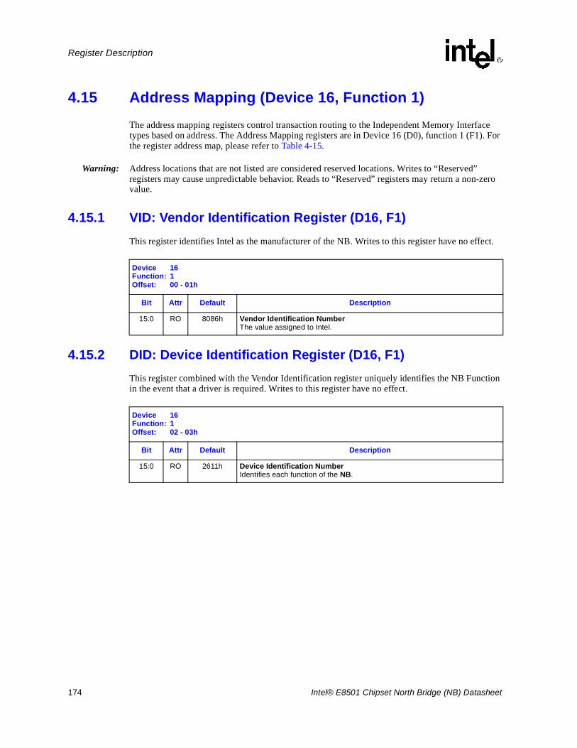
174 Intel® E8501 Chipset North Bridge (NB) Datasheet
Register Description
4.15 Address Mapping (Device 16, Function 1)The address mapping registers control transaction routing to the Independent Memory Interface types based on address. The Address Mapping registers are in Device 16 (D0), function 1 (F1). For the register address map, please refer to Table 4-15.
Warning: Address locations that are not listed are considered reserved locations. Writes to “Reserved” registers may cause unpredictable behavior. Reads to “Reserved” registers may return a non-zero value.
4.15.1 VID: Vendor Identification Register (D16, F1)This register identifies Intel as the manufacturer of the NB. Writes to this register have no effect.
4.15.2 DID: Device Identification Register (D16, F1)This register combined with the Vendor Identification register uniquely identifies the NB Function in the event that a driver is required. Writes to this register have no effect.
Device 16Function: 1Offset: 00 - 01h
Bit Attr Default Description
15:0 RO 8086h Vendor Identification NumberThe value assigned to Intel.
Device 16Function: 1Offset: 02 - 03h
Bit Attr Default Description
15:0 RO 2611h Device Identification Number Identifies each function of the NB.
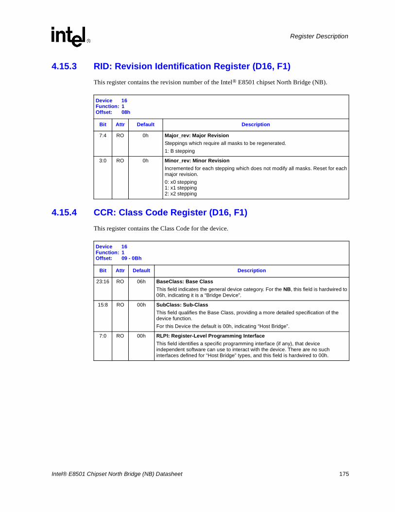
Intel® E8501 Chipset North Bridge (NB) Datasheet 175
Register Description
4.15.3 RID: Revision Identification Register (D16, F1)This register contains the revision number of the Intel® E8501 chipset North Bridge (NB).
4.15.4 CCR: Class Code Register (D16, F1)This register contains the Class Code for the device.
Device 16Function: 1Offset: 08h
Bit Attr Default Description
7:4 RO 0h Major_rev: Major RevisionSteppings which require all masks to be regenerated.1: B stepping
3:0 RO 0h Minor_rev: Minor RevisionIncremented for each stepping which does not modify all masks. Reset for eachmajor revision.0: x0 stepping1: x1 stepping2: x2 stepping
Device 16Function: 1Offset: 09 - 0Bh
Bit Attr Default Description
23:16 RO 06h BaseClass: Base ClassThis field indicates the general device category. For the NB, this field is hardwired to06h, indicating it is a “Bridge Device”.
15:8 RO 00h SubClass: Sub-ClassThis field qualifies the Base Class, providing a more detailed specification of the device function. For this Device the default is 00h, indicating “Host Bridge”.
7:0 RO 00h RLPI: Register-Level Programming InterfaceThis field identifies a specific programming interface (if any), that device independent software can use to interact with the device. There are no such interfaces defined for “Host Bridge” types, and this field is hardwired to 00h.
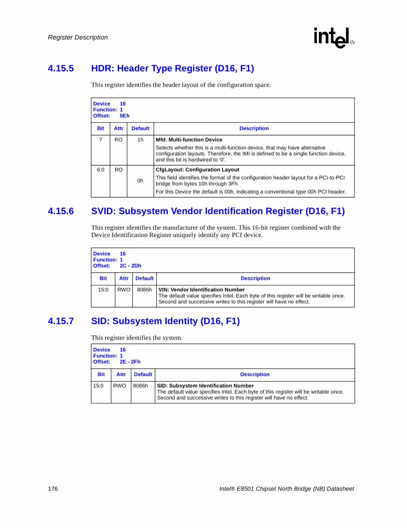
176 Intel® E8501 Chipset North Bridge (NB) Datasheet
Register Description
4.15.5 HDR: Header Type Register (D16, F1)This register identifies the header layout of the configuration space.
4.15.6 SVID: Subsystem Vendor Identification Register (D16, F1)This register identifies the manufacturer of the system. This 16-bit register combined with the Device Identification Register uniquely identify any PCI device.
4.15.7 SID: Subsystem Identity (D16, F1)This register identifies the system.
Device 16Function: 1Offset: 0Eh
Bit Attr Default Description
7 RO 1h Mfd: Multi-function DeviceSelects whether this is a multi-function device, that may have alternative configuration layouts. Therefore, the IMI is defined to be a single function device, and this bit is hardwired to ‘0’.
6:0 RO
0h
CfgLayout: Configuration LayoutThis field identifies the format of the configuration header layout for a PCI-to-PCI bridge from bytes 10h through 3Fh. For this Device the default is 00h, indicating a conventional type 00h PCI header.
Device 16Function: 1Offset: 2C - 2Dh
Bit Attr Default Description
15:0 RWO 8086h VIN: Vendor Identification NumberThe default value specifies Intel. Each byte of this register will be writable once. Second and successive writes to this register will have no effect.
Device 16Function: 1Offset: 2E - 2Fh
Bit Attr Default Description
15:0 RWO 8086h SID: Subsystem Identification Number The default value specifies Intel. Each byte of this register will be writable once. Second and successive writes to this register will have no effect.
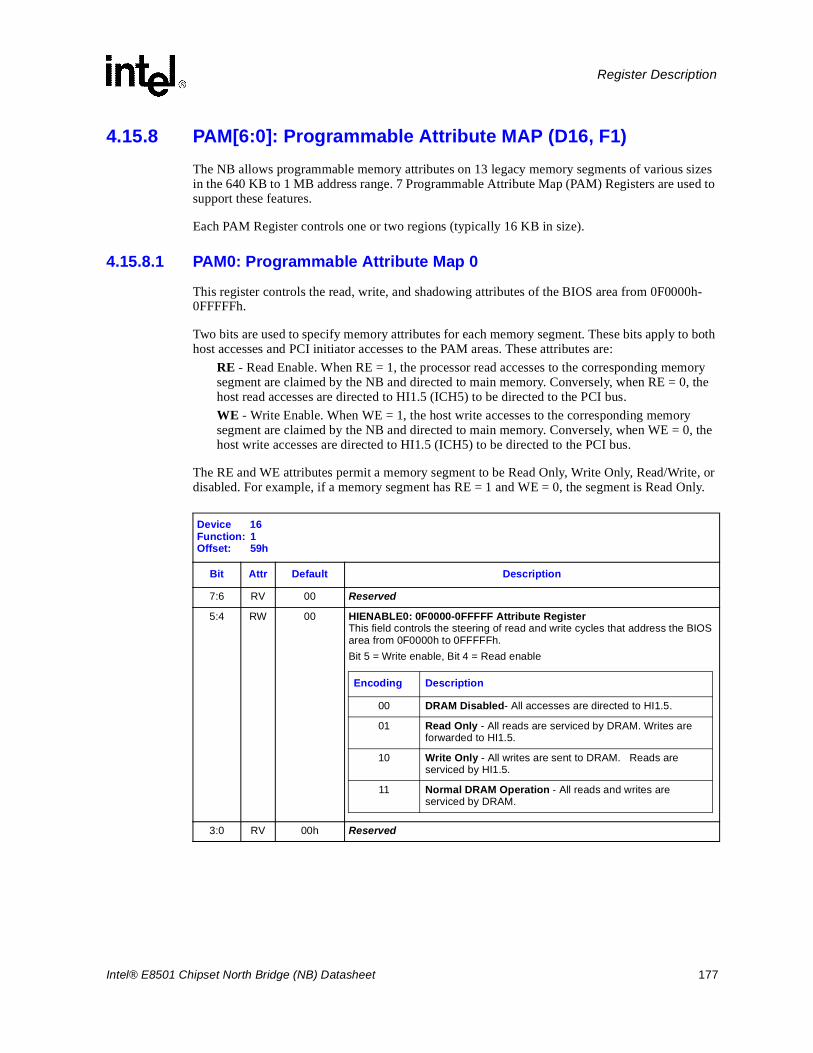
Intel® E8501 Chipset North Bridge (NB) Datasheet 177
Register Description
4.15.8 PAM[6:0]: Programmable Attribute MAP (D16, F1)The NB allows programmable memory attributes on 13 legacy memory segments of various sizes in the 640 KB to 1 MB address range. 7 Programmable Attribute Map (PAM) Registers are used to support these features.
Each PAM Register controls one or two regions (typically 16 KB in size).
4.15.8.1 PAM0: Programmable Attribute Map 0
This register controls the read, write, and shadowing attributes of the BIOS area from 0F0000h-0FFFFFh.
Two bits are used to specify memory attributes for each memory segment. These bits apply to both host accesses and PCI initiator accesses to the PAM areas. These attributes are:
RE - Read Enable. When RE = 1, the processor read accesses to the corresponding memory segment are claimed by the NB and directed to main memory. Conversely, when RE = 0, the host read accesses are directed to HI1.5 (ICH5) to be directed to the PCI bus.WE - Write Enable. When WE = 1, the host write accesses to the corresponding memory segment are claimed by the NB and directed to main memory. Conversely, when WE = 0, the host write accesses are directed to HI1.5 (ICH5) to be directed to the PCI bus.
The RE and WE attributes permit a memory segment to be Read Only, Write Only, Read/Write, or disabled. For example, if a memory segment has RE = 1 and WE = 0, the segment is Read Only.
Device 16Function: 1Offset: 59h
Bit Attr Default Description
7:6 RV 00 Reserved
5:4 RW 00 HIENABLE0: 0F0000-0FFFFF Attribute RegisterThis field controls the steering of read and write cycles that address the BIOS area from 0F0000h to 0FFFFFh.Bit 5 = Write enable, Bit 4 = Read enable.
3:0 RV 00h Reserved
Encoding Description
00 DRAM Disabled- All accesses are directed to HI1.5.
01 Read Only - All reads are serviced by DRAM. Writes are forwarded to HI1.5.
10 Write Only - All writes are sent to DRAM. Reads are serviced by HI1.5.
11 Normal DRAM Operation - All reads and writes are serviced by DRAM.
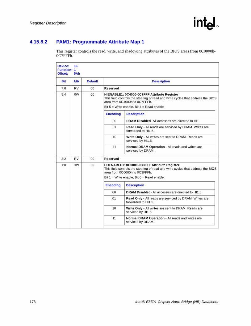
178 Intel® E8501 Chipset North Bridge (NB) Datasheet
Register Description
4.15.8.2 PAM1: Programmable Attribute Map 1
This register controls the read, write, and shadowing attributes of the BIOS areas from 0C0000h-0C7FFFh.
Device: 16Function: 1Offset: 5Ah
Bit Attr Default Description
7:6 RV 00 Reserved
5:4 RW 00 HIENABLE1: 0C4000-0C7FFF Attribute RegisterThis field controls the steering of read and write cycles that address the BIOS area from 0C4000h to 0C7FFFh.Bit 5 = Write enable, Bit 4 = Read enable.
3:2 RV 00 Reserved
1:0 RW 00 LOENABLE1: 0C0000-0C3FFF Attribute RegisterThis field controls the steering of read and write cycles that address the BIOS area from 0C0000h to 0C3FFFh.Bit 1 = Write enable, Bit 0 = Read enable.
Encoding Description
00 DRAM Disabled- All accesses are directed to HI1.
01 Read Only - All reads are serviced by DRAM. Writes are forwarded to HI1.5.
10 Write Only - All writes are sent to DRAM. Reads are serviced by HI1.5.
11 Normal DRAM Operation - All reads and writes are serviced by DRAM.
Encoding Description
00 DRAM Disabled- All accesses are directed to HI1.5.
01 Read Only - All reads are serviced by DRAM. Writes are forwarded to HI1.5.
10 Write Only - All writes are sent to DRAM. Reads are serviced by HI1.5.
11 Normal DRAM Operation - All reads and writes are serviced by DRAM.
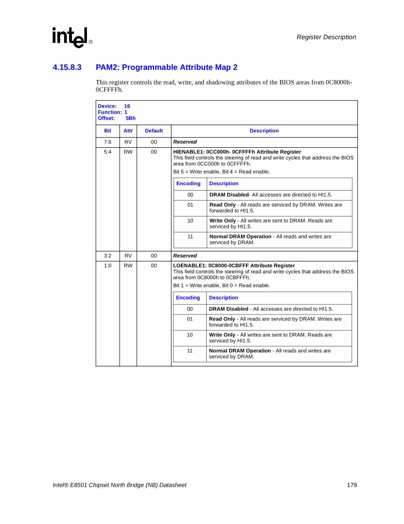
Intel® E8501 Chipset North Bridge (NB) Datasheet 179
Register Description
4.15.8.3 PAM2: Programmable Attribute Map 2
This register controls the read, write, and shadowing attributes of the BIOS areas from 0C8000h-0CFFFFh.
Device: 16Function: 1Offset: 5Bh
Bit Attr Default Description
7:6 RV 00 Reserved
5:4 RW 00 HIENABLE1: 0CC000h- 0CFFFFh Attribute RegisterThis field controls the steering of read and write cycles that address the BIOS area from 0CC000h to 0CFFFFh.Bit 5 = Write enable, Bit 4 = Read enable.
3:2 RV 00 Reserved
1:0 RW 00 LOENABLE1: 0C8000-0CBFFF Attribute RegisterThis field controls the steering of read and write cycles that address the BIOS area from 0C8000h to 0CBFFFh.Bit 1 = Write enable, Bit 0 = Read enable.
Encoding Description
00 DRAM Disabled- All accesses are directed to HI1.5.
01 Read Only - All reads are serviced by DRAM. Writes are forwarded to HI1.5.
10 Write Only - All writes are sent to DRAM. Reads are serviced by HI1.5.
11 Normal DRAM Operation - All reads and writes are serviced by DRAM.
Encoding Description
00 DRAM Disabled - All accesses are directed to HI1.5.
01 Read Only - All reads are serviced by DRAM. Writes are forwarded to HI1.5.
10 Write Only - All writes are sent to DRAM. Reads are serviced by HI1.5.
11 Normal DRAM Operation - All reads and writes are serviced by DRAM.
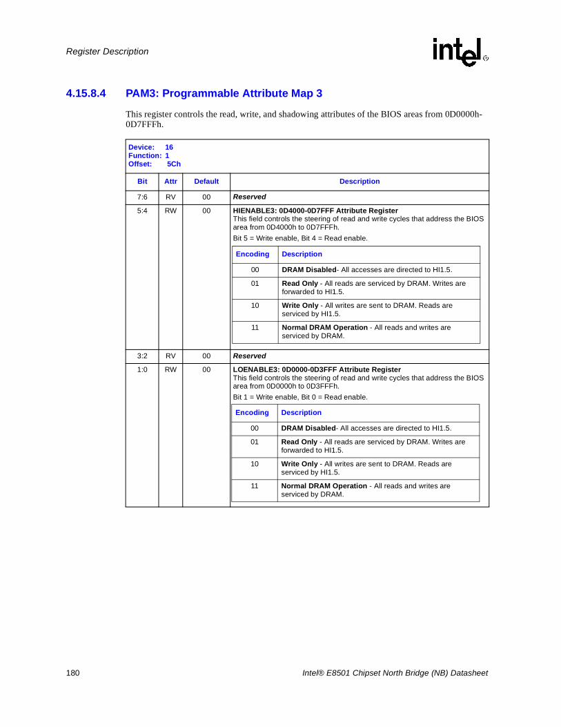
180 Intel® E8501 Chipset North Bridge (NB) Datasheet
Register Description
4.15.8.4 PAM3: Programmable Attribute Map 3
This register controls the read, write, and shadowing attributes of the BIOS areas from 0D0000h-0D7FFFh.
Device: 16Function: 1Offset: 5Ch
Bit Attr Default Description
7:6 RV 00 Reserved
5:4 RW 00 HIENABLE3: 0D4000-0D7FFF Attribute RegisterThis field controls the steering of read and write cycles that address the BIOS area from 0D4000h to 0D7FFFh.Bit 5 = Write enable, Bit 4 = Read enable.
3:2 RV 00 Reserved
1:0 RW 00 LOENABLE3: 0D0000-0D3FFF Attribute RegisterThis field controls the steering of read and write cycles that address the BIOS area from 0D0000h to 0D3FFFh.Bit 1 = Write enable, Bit 0 = Read enable.
Encoding Description
00 DRAM Disabled- All accesses are directed to HI1.5.
01 Read Only - All reads are serviced by DRAM. Writes are forwarded to HI1.5.
10 Write Only - All writes are sent to DRAM. Reads are serviced by HI1.5.
11 Normal DRAM Operation - All reads and writes are serviced by DRAM.
Encoding Description
00 DRAM Disabled- All accesses are directed to HI1.5.
01 Read Only - All reads are serviced by DRAM. Writes are forwarded to HI1.5.
10 Write Only - All writes are sent to DRAM. Reads are serviced by HI1.5.
11 Normal DRAM Operation - All reads and writes are serviced by DRAM.
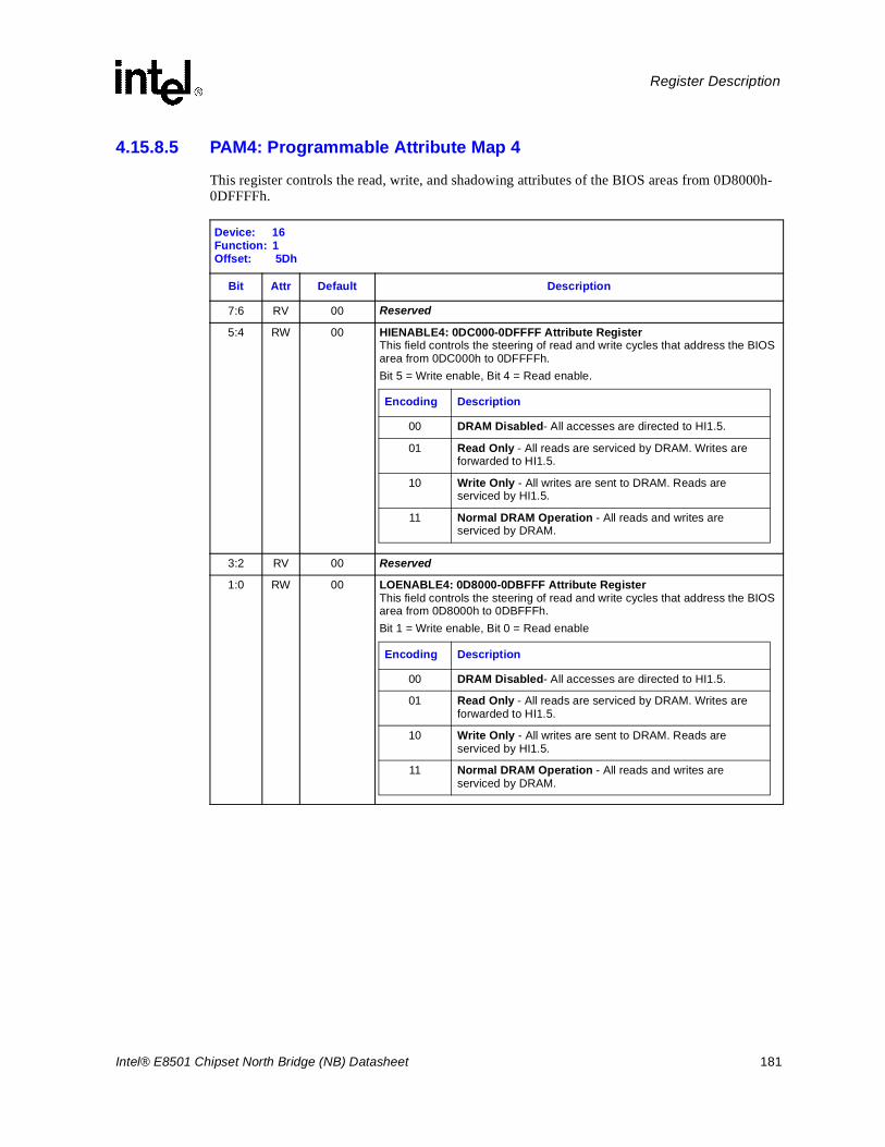
Intel® E8501 Chipset North Bridge (NB) Datasheet 181
Register Description
4.15.8.5 PAM4: Programmable Attribute Map 4
This register controls the read, write, and shadowing attributes of the BIOS areas from 0D8000h-0DFFFFh.
Device: 16Function: 1Offset: 5Dh
Bit Attr Default Description
7:6 RV 00 Reserved
5:4 RW 00 HIENABLE4: 0DC000-0DFFFF Attribute RegisterThis field controls the steering of read and write cycles that address the BIOS area from 0DC000h to 0DFFFFh.Bit 5 = Write enable, Bit 4 = Read enable.
3:2 RV 00 Reserved
1:0 RW 00 LOENABLE4: 0D8000-0DBFFF Attribute RegisterThis field controls the steering of read and write cycles that address the BIOS area from 0D8000h to 0DBFFFh.Bit 1 = Write enable, Bit 0 = Read enable
Encoding Description
00 DRAM Disabled- All accesses are directed to HI1.5.
01 Read Only - All reads are serviced by DRAM. Writes are forwarded to HI1.5.
10 Write Only - All writes are sent to DRAM. Reads are serviced by HI1.5.
11 Normal DRAM Operation - All reads and writes are serviced by DRAM.
Encoding Description
00 DRAM Disabled- All accesses are directed to HI1.5.
01 Read Only - All reads are serviced by DRAM. Writes are forwarded to HI1.5.
10 Write Only - All writes are sent to DRAM. Reads are serviced by HI1.5.
11 Normal DRAM Operation - All reads and writes are serviced by DRAM.
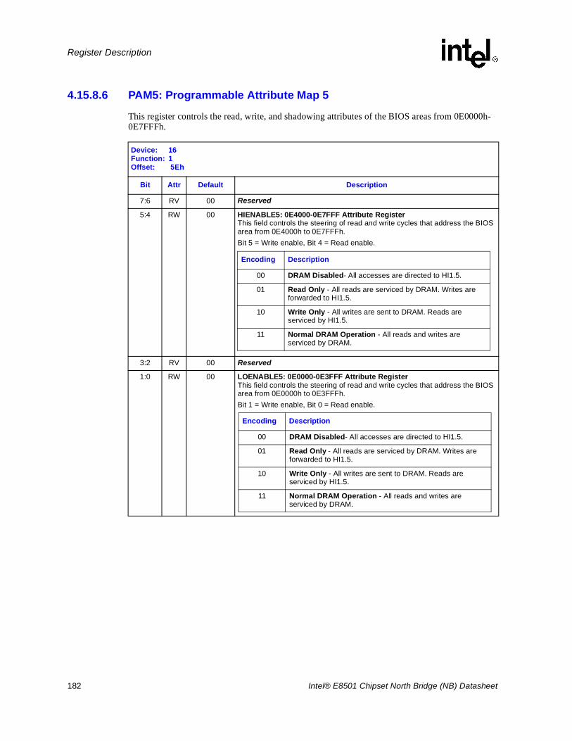
182 Intel® E8501 Chipset North Bridge (NB) Datasheet
Register Description
4.15.8.6 PAM5: Programmable Attribute Map 5
This register controls the read, write, and shadowing attributes of the BIOS areas from 0E0000h-0E7FFFh.
Device: 16Function: 1Offset: 5Eh
Bit Attr Default Description
7:6 RV 00 Reserved
5:4 RW 00 HIENABLE5: 0E4000-0E7FFF Attribute RegisterThis field controls the steering of read and write cycles that address the BIOS area from 0E4000h to 0E7FFFh.Bit 5 = Write enable, Bit 4 = Read enable.
3:2 RV 00 Reserved
1:0 RW 00 LOENABLE5: 0E0000-0E3FFF Attribute RegisterThis field controls the steering of read and write cycles that address the BIOS area from 0E0000h to 0E3FFFh.Bit 1 = Write enable, Bit 0 = Read enable.
Encoding Description
00 DRAM Disabled- All accesses are directed to HI1.5.
01 Read Only - All reads are serviced by DRAM. Writes are forwarded to HI1.5.
10 Write Only - All writes are sent to DRAM. Reads are serviced by HI1.5.
11 Normal DRAM Operation - All reads and writes are serviced by DRAM.
Encoding Description
00 DRAM Disabled- All accesses are directed to HI1.5.
01 Read Only - All reads are serviced by DRAM. Writes are forwarded to HI1.5.
10 Write Only - All writes are sent to DRAM. Reads are serviced by HI1.5.
11 Normal DRAM Operation - All reads and writes are serviced by DRAM.

Intel® E8501 Chipset North Bridge (NB) Datasheet 183
Register Description
4.15.8.7 PAM6: Programmable Attribute Map 6
This register controls the read, write, and shadowing attributes of the BIOS areas from 0E8000h-0EFFFFh.
Device: 16Function: 1Offset: 5Fh
Bit Attr Default Description
7:6 RV 00 Reserved
5:4 RW 00 HIENABLE4: 0EC000-0EFFFF Attribute RegisterThis field controls the steering of read and write cycles that address the BIOS area from 0EC000h to 0DFFFFh.Bit 5 = Write enable, Bit 4 = Read enable.
3:2 RV 00 Reserved
1:0 RW 00 LOENABLE4: 0E8000-0EBFFF Attribute RegisterThis field controls the steering of read and write cycles that address the BIOS area from 0E8000h to 0EBFFFh.Bit 1 = Write enable, Bit 0 = Read enable.
Encoding Description
00 DRAM Disabled- All accesses are directed to HI1.5.
01 Read Only - All reads are serviced by DRAM. Writes are forwarded to HI1.5.
10 Write Only - All writes are sent to DRAM. Reads are serviced by HI1.5.
11 Normal DRAM Operation - All reads and writes are serviced by DRAM.b
Encoding Description
00 DRAM Disabled- All accesses are directed to HI1.5.
01 Read Only - All reads are serviced by DRAM. Writes are forwarded to HI1.5.
10 Write Only - All writes are sent to DRAM. Reads are serviced by HI1.5.
11 Normal DRAM Operation - All reads and writes are serviced by DRAM.
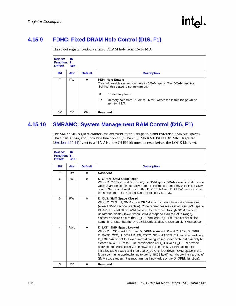
184 Intel® E8501 Chipset North Bridge (NB) Datasheet
Register Description
4.15.9 FDHC: Fixed DRAM Hole Control (D16, F1)This 8-bit register controls a fixed DRAM hole from 15-16 MB.
4.15.10 SMRAMC: System Management RAM Control (D16, F1)The SMRAMC register controls the accessibility to Compatible and Extended SMRAM spaces. The Open, Close, and Lock bits function only when G_SMRAME bit in EXSMRC Register (Section 4.15.11) is set to a “1”. Also, the OPEN bit must be reset before the LOCK bit is set.
Device: 16Function: 1Offset: 60h
Bit Attr Default Description
7 RW 0 HEN: Hole Enable This field enables a memory hole in DRAM space. The DRAM that lies “behind” this space is not remapped.
6:0 RV 00h Reserved
0: No memory hole.
1: Memory hole from 15 MB to 16 MB. Accesses in this range will be sent to HI1.5.
Device: 16Function: 1Offset: 61h
Bit Attr Default Description
7 RV 0 Reserved
6 RWL 0 D_OPEN: SMM Space OpenWhen D_OPEN=1 and D_LCK=0, the SMM space DRAM is made visible even when SMM decode is not active. This is intended to help BIOS initialize SMM space. Software should ensure that D_OPEN=1 and D_CLS=1 are not set at the same time. This register can be locked by D_LCK.
5 RW 0 D_CLS: SMM Space ClosedWhen D_CLS = 1, SMM space DRAM is not accessible to data references (even if SMM decode is active). Code references may still access SMM space DRAM. This will allow SMM software to reference through SMM space to update the display (even when SMM is mapped over the VGA range). Software should ensure that D_OPEN=1 and D_CLS=1 are not set at the same time. Note that the D_CLS bit only applies to Compatible SMM space.
4 RWL 0 D_LCK: SMM Space LockedWhen D_LCK is set to 1, then D_OPEN is reset to 0 and D_LCK, D_OPEN, C_BASE_SEG, H_SMRAM_EN, TSEG_SZ and TSEG_EN become read only. D_LCK can be set to 1 via a normal configuration space write but can only be cleared by a Full Reset. The combination of D_LCK and D_OPEN provide convenience with security. The BIOS can use the D_OPEN function to initialize SMM space and then use D_LCK to “lock down” SMM space in the future so that no application software (or BIOS itself) can violate the integrity of SMM space (even if the program has knowledge of the D_OPEN function).
3 RV 0 Reserved
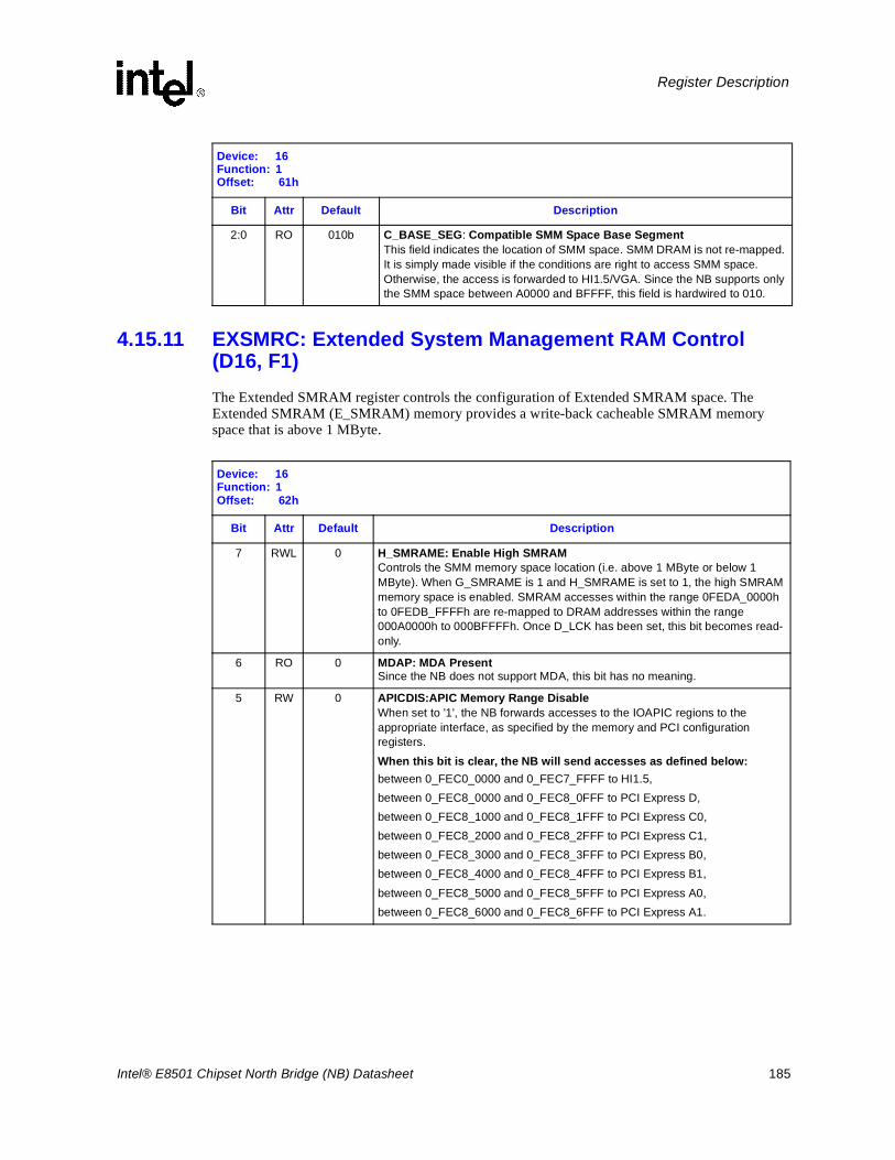
Intel® E8501 Chipset North Bridge (NB) Datasheet 185
Register Description
4.15.11 EXSMRC: Extended System Management RAM Control (D16, F1)The Extended SMRAM register controls the configuration of Extended SMRAM space. The Extended SMRAM (E_SMRAM) memory provides a write-back cacheable SMRAM memory space that is above 1 MByte.
2:0 RO 010b C_BASE_SEG: Compatible SMM Space Base SegmentThis field indicates the location of SMM space. SMM DRAM is not re-mapped. It is simply made visible if the conditions are right to access SMM space. Otherwise, the access is forwarded to HI1.5/VGA. Since the NB supports only the SMM space between A0000 and BFFFF, this field is hardwired to 010.
Device: 16Function: 1Offset: 61h
Bit Attr Default Description
Device: 16Function: 1Offset: 62h
Bit Attr Default Description
7 RWL 0 H_SMRAME: Enable High SMRAM Controls the SMM memory space location (i.e. above 1 MByte or below 1 MByte). When G_SMRAME is 1 and H_SMRAME is set to 1, the high SMRAM memory space is enabled. SMRAM accesses within the range 0FEDA_0000h to 0FEDB_FFFFh are re-mapped to DRAM addresses within the range 000A0000h to 000BFFFFh. Once D_LCK has been set, this bit becomes read- only.
6 RO 0 MDAP: MDA Present Since the NB does not support MDA, this bit has no meaning.
5 RW 0 APICDIS:APIC Memory Range DisableWhen set to '1', the NB forwards accesses to the IOAPIC regions to the appropriate interface, as specified by the memory and PCI configuration registers.
When this bit is clear, the NB will send accesses as defined below:between 0_FEC0_0000 and 0_FEC7_FFFF to HI1.5,between 0_FEC8_0000 and 0_FEC8_0FFF to PCI Express D, between 0_FEC8_1000 and 0_FEC8_1FFF to PCI Express C0,between 0_FEC8_2000 and 0_FEC8_2FFF to PCI Express C1,between 0_FEC8_3000 and 0_FEC8_3FFF to PCI Express B0, between 0_FEC8_4000 and 0_FEC8_4FFF to PCI Express B1,
between 0_FEC8_5000 and 0_FEC8_5FFF to PCI Express A0,between 0_FEC8_6000 and 0_FEC8_6FFF to PCI Express A1.
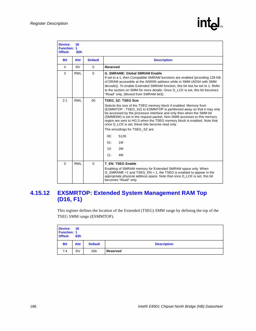
186 Intel® E8501 Chipset North Bridge (NB) Datasheet
Register Description
4.15.12 EXSMRTOP: Extended System Management RAM Top(D16, F1)
This register defines the location of the Extended (TSEG) SMM range by defining the top of the TSEG SMM range (ESMMTOP).
4 RV 0 Reserved
3 RWL 0 G_SMRAME: Global SMRAM Enable If set to a 1, then Compatible SMRAM functions are enabled (providing 128 KB of DRAM accessible at the A0000h address while in SMM (ADS# with SMM decode)). To enable Extended SMRAM function, this bit has be set to 1. Refer to the section on SMM for more details. Once D_LCK is set, this bit becomes “Read” only. (Moved from SMRAM bit3).
2:1 RWL 00 TSEG_SZ: TSEG SizeSelects the size of the TSEG memory block if enabled. Memory from (ESMMTOP - TSEG_SZ) to ESMMTOP is partitioned away so that it may only be accessed by the processor interface and only then when the SMM bit (SMMEM#) is set in the request packet. Non-SMM accesses to this memory region are sent to HI1.5 when the TSEG memory block is enabled. Note that once D_LCK is set, these bits become read only. The encodings for TSEG_SZ are:
0 RWL 0 T_EN: TSEG EnableEnabling of SMRAM memory for Extended SMRAM space only. When G_SMRAME =1 and TSEG_EN = 1, the TSEG is enabled to appear in the appropriate physical address space. Note that once D_LCK is set, this bit becomes “Read” only.
Device: 16Function: 1Offset: 62h
Bit Attr Default Description
00: 512K
01: 1M
10: 2M
11: 4M
Device: 16Function: 1Offset: 63h
Bit Attr Default Description
7:4 RV 00h Reserved
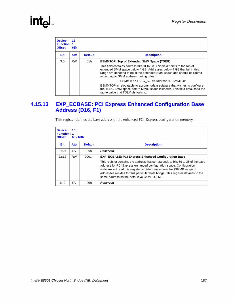
Intel® E8501 Chipset North Bridge (NB) Datasheet 187
Register Description
4.15.13 EXP_ECBASE: PCI Express Enhanced Configuration Base Address (D16, F1)This register defines the base address of the enhanced PCI Express configuration memory.
3:0 RW 01h ESMMTOP: Top of Extended SMM Space (TSEG)This field contains address bits 31 to 28. This field points to the top of extended SMM space below 4 GB. Addresses below 4 GB that fall in this range are decoded to be in the extended SMM space and should be routed according to SMM address routing rules:
ESMMTOP-TSEG_SZ <= Address < ESMMTOPESMMTOP is relocatable to accommodate software that wishes to configure the TSEG SMM space before MMIO space is known. This field defaults to the same value that TOLM defaults to.
Device: 16Function: 1Offset: 63h
Bit Attr Default Description
Device: 16Function: 1Offset: 68 - 6Bh
Bit Attr Default Description
31:24 RV 00h Reserved
23:12 RW 0001h EXP_ECBASE: PCI Express Enhanced Configuration BaseThis register contains the address that corresponds to bits 39 to 28 of the base address for PCI Express enhanced configuration space. Configuration software will read this register to determine where the 256 MB range of addresses resides for this particular host bridge. This register defaults to the same address as the default value for TOLM.
11:0 RV 00h Reserved
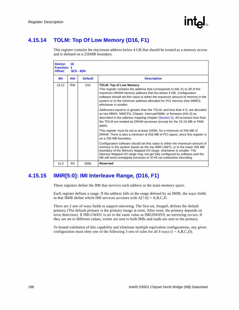
188 Intel® E8501 Chipset North Bridge (NB) Datasheet
Register Description
4.15.14 TOLM: Top Of Low Memory (D16, F1)This register contains the maximum address below 4 GB that should be treated as a memory access and is defined on a 256MB boundary.
4.15.15 IMIR[5:0]: IMI Interleave Range, (D16, F1)These registers define the IMI that services each address in the main memory space.
Each register defines a range. If the address falls in the range defined by an IMIR, the ways fields in that IMIR define which IMI services accesses with A[7:6] = A,B,C,D.
There are 2 sets of ways fields to support mirroring. The first set, Image0, defines the default primary (The default primary is the primary image at reset. After reset, the primary depends on error detection). If IMG1WAYi is set to the same value as IMG0WAY0, no mirroring occurs. If they are set to different values, writes are sent to both IMIs and reads are sent to the primary.
To bound validation of this capability and eliminate multiple equivalent configurations, any given configuration must obey one of the following 3 sets of rules for all 4 ways (i = A,B,C,D).
Device: 16Function: 1Offset: 6Ch - 6Dh
Bit Attr Default Description
15:12 RW 01h TOLM: Top of Low MemoryThis register contains the address that corresponds to bits 31 to 28 of the maximum DRAM memory address that lies below 4 GB. Configuration software should set this value to either the maximum amount of memory in the system or to the minimum address allocated for PCI memory (low MMIO), whichever is smaller.
Addresses equal to or greater than the TOLM, and less than 4 G, are decoded as low MMIO, MMCFG, Chipset, Interrupt/SMM, or firmware (HI1.5) as described in the address mapping chapter (Section 5). All accesses less than the TOLM are treated as DRAM accesses (except for the 15-16 MB or PAM gaps).
This register must be set to at least 1000h, for a minimum of 256 MB of DRAM. There is also a minimum of 256 MB of PCI space, since this register is on a 256 MB boundary.Configuration software should set this value to either the maximum amount of memory in the system (same as the top IMIR.LIMIT), or to the lower 256 MB boundary of the Memory Mapped I/O range, whichever is smaller. The Memory Mapped I/O range may not get fully configured by software and the NB will send unmapped accesses to ICH5 via subtractive decoding.
11:0 RV 000h Reserved
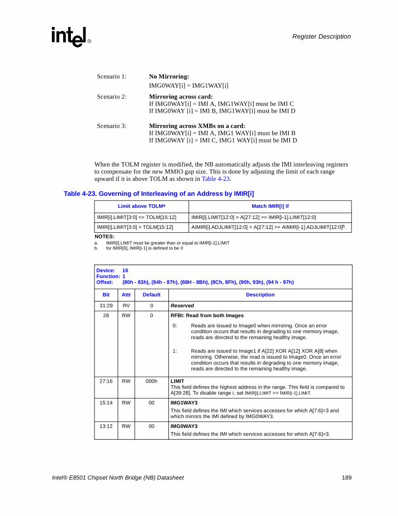
Intel® E8501 Chipset North Bridge (NB) Datasheet 189
Register Description
:
When the TOLM register is modified, the NB automatically adjusts the IMI interleaving registers to compensate for the new MMIO gap size. This is done by adjusting the limit of each range upward if it is above TOLM as shown in Table 4-23.
Scenario 1: No Mirroring:IMG0WAY[i] = IMG1WAY[i]
Scenario 2: Mirroring across card:If IMG0WAY[i] = IMI A, IMG1WAY[i] must be IMI C If IMG0WAY [i] = IMI B, IMG1WAY[i] must be IMI D
Scenario 3: Mirroring across XMBs on a card:If IMG0WAY[i] = IMI A, IMG1 WAY[i] must be IMI BIf IMG0WAY [i] = IMI C, IMG1 WAY[i] must be IMI D
Table 4-23. Governing of Interleaving of an Address by IMIR[i]
Limit above TOLMa
NOTES:a. IMIR[i].LIMIT must be greater than or equal to IMIR[i-1].LIMIT
Match IMIR[i] if
IMIR[i].LIMIT[3:0] <= TOLM[15:12] IMIR[i].LIMIT[12:0] > A[27:12] >= IMIR[i-1].LIMIT[12:0]
IMIR[i].LIMIT[3:0] > TOLM[15:12] AIMIR[i].ADJLIMIT[12:0] > A[27:12] >= AIMIR[i-1].ADJLIMIT[12:0]b.
b. for IMIR[0], IMIR[i-1] is defined to be 0
Device: 16Function: 1Offset: (80h - 83h), (84h - 87h), (88H - 8Bh), (8Ch, 8Fh), (90h, 93h), (94 h - 97h)
Bit Attr Default Description
31:29 RV 0 Reserved
28 RW 0 RFBI: Read from both Images
27:16 RW 000h LIMITThis field defines the highest address in the range. This field is compared to A[39:28]. To disable range i, set IMIR[i].LIMIT == IMIR[i-1].LIMIT.
15:14 RW 00 IMG1WAY3This field defines the IMI which services accesses for which A[7:6]=3 and which mirrors the IMI defined by IMG0WAY3.
13:12 RW 00 IMG0WAY3This field defines the IMI which services accesses for which A[7:6]=3.
0: Reads are issued to Image0 when mirroring. Once an error condition occurs that results in degrading to one memory image, reads are directed to the remaining healthy image.
1: Reads are issued to Image1 if A[22] XOR A[12] XOR A[8] when mirroring. Otherwise, the read is issued to Image0. Once an error condition occurs that results in degrading to one memory image, reads are directed to the remaining healthy image.
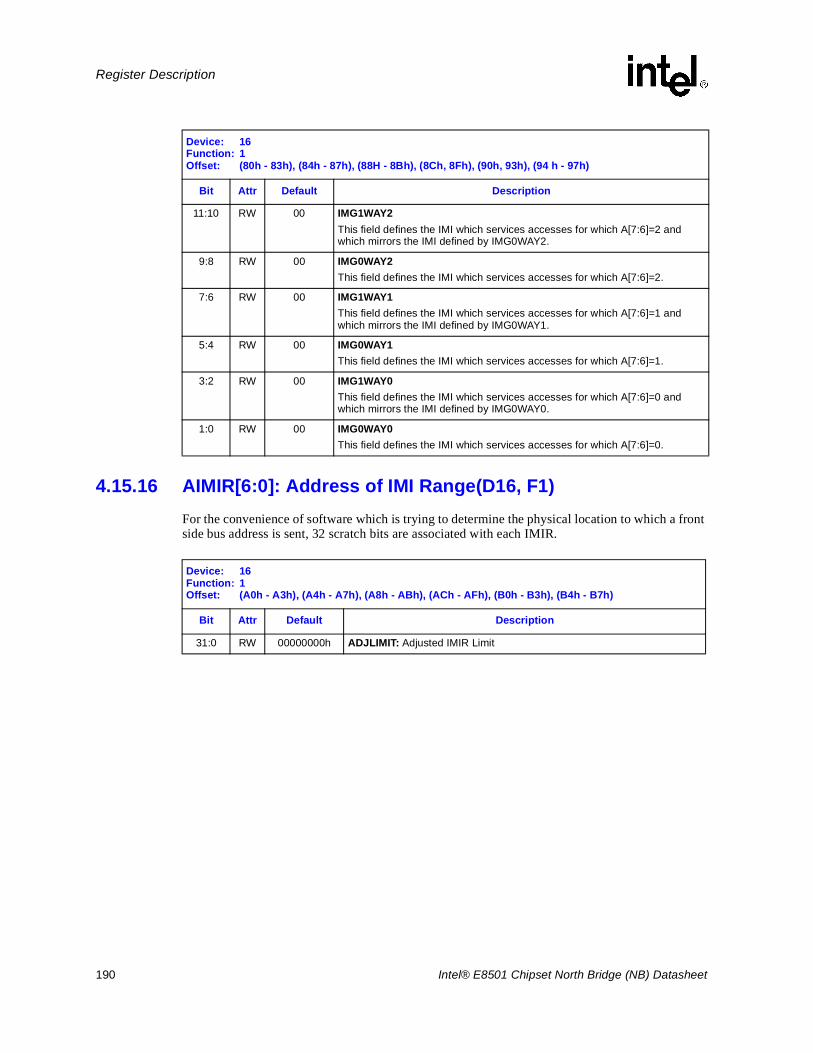
190 Intel® E8501 Chipset North Bridge (NB) Datasheet
Register Description
4.15.16 AIMIR[6:0]: Address of IMI Range(D16, F1)For the convenience of software which is trying to determine the physical location to which a front side bus address is sent, 32 scratch bits are associated with each IMIR.
11:10 RW 00 IMG1WAY2This field defines the IMI which services accesses for which A[7:6]=2 and which mirrors the IMI defined by IMG0WAY2.
9:8 RW 00 IMG0WAY2This field defines the IMI which services accesses for which A[7:6]=2.
7:6 RW 00 IMG1WAY1This field defines the IMI which services accesses for which A[7:6]=1 and which mirrors the IMI defined by IMG0WAY1.
5:4 RW 00 IMG0WAY1This field defines the IMI which services accesses for which A[7:6]=1.
3:2 RW 00 IMG1WAY0This field defines the IMI which services accesses for which A[7:6]=0 and which mirrors the IMI defined by IMG0WAY0.
1:0 RW 00 IMG0WAY0This field defines the IMI which services accesses for which A[7:6]=0.
Device: 16Function: 1Offset: (80h - 83h), (84h - 87h), (88H - 8Bh), (8Ch, 8Fh), (90h, 93h), (94 h - 97h)
Bit Attr Default Description
Device: 16Function: 1Offset: (A0h - A3h), (A4h - A7h), (A8h - ABh), (ACh - AFh), (B0h - B3h), (B4h - B7h)
Bit Attr Default Description
31:0 RW 00000000h ADJLIMIT: Adjusted IMIR Limit
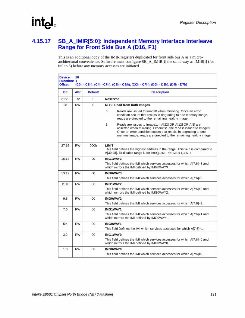
Intel® E8501 Chipset North Bridge (NB) Datasheet 191
Register Description
4.15.17 SB_A_IMIR[5:0]: Independent Memory Interface Interleave Range for Front Side Bus A (D16, F1)This is an additional copy of the IMIR registers duplicated for front side bus A as a micro-architectural convenience. Software must configure SB_A_IMIR[i] the same way as IMIR[i] (for i=0 to 5) before any memory accesses are initiated.
Device: 16Function: 1Offset: (C0h - C3h), (C4h -C7h), (C8h - CBh), (CCh - CFh), (D0h - D3h), (D4h - D7h)
Bit Attr Default Description
31:29 RV 0 Reserved
28 RW 0 RFBI. Read from both Images
27:16 RW 000h LIMITThis field defines the highest address in the range. This field is compared to A[39:28]. To disable range i, set IMIR[i].LIMIT == IMIR[i-1].LIMIT.
15:14 RW 00 IMG1WAY3This field defines the IMI which services accesses for which A[7:6]=3 and which mirrors the IMI defined by IMG0WAY3.
13:12 RW 00 IMG0WAY3This field defines the IMI which services accesses for which A[7:6]=3.
11:10 RW 00 IMG1WAY2This field defines the IMI which services accesses for which A[7:6]=2 and which mirrors the IMI defined by IMG0WAY2.
9:8 RW 00 IMG0WAY2This field defines the IMI which services accesses for which A[7:6]=2.
7:6 RW 00 IMG1WAY1This field defines the IMI which services accesses for which A[7:6]=1 and which mirrors the IMI defined by IMG0WAY1.
5:4 RW 00 IMG0WAY1This field Defines the IMI which services accesses for which A[7:6]=1.
3:2 RW 00 IMG1WAY0This field defines the IMI which services accesses for which A[7:6]=0 and which mirrors the IMI defined by IMG0WAY0.
1:0 RW 00 IMG0WAY0This field defines the IMI which services accesses for which A[7:6]=0.
0: Reads are issued to Image0 when mirroring. Once an error condition occurs that results in degrading to one memory image, reads are directed to the remaining healthy image.
1: Reads are issues to Image1, if A[22] OR A[12] OR A[8] are asserted when mirroring. Otherwise, the read is issued to Image0. Once an error condition occurs that results in degrading to one memory image, reads are directed to the remaining healthy image.
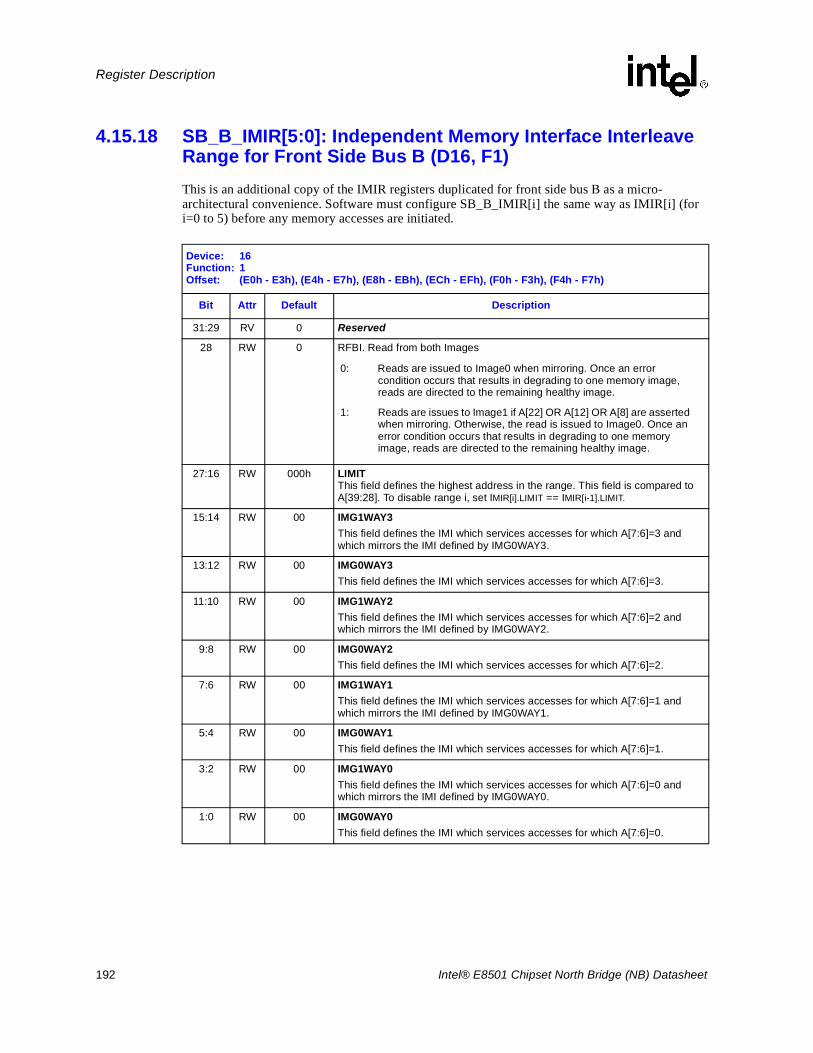
192 Intel® E8501 Chipset North Bridge (NB) Datasheet
Register Description
4.15.18 SB_B_IMIR[5:0]: Independent Memory Interface Interleave Range for Front Side Bus B (D16, F1)This is an additional copy of the IMIR registers duplicated for front side bus B as a micro-architectural convenience. Software must configure SB_B_IMIR[i] the same way as IMIR[i] (for i=0 to 5) before any memory accesses are initiated.
Device: 16Function: 1Offset: (E0h - E3h), (E4h - E7h), (E8h - EBh), (ECh - EFh), (F0h - F3h), (F4h - F7h)
Bit Attr Default Description
31:29 RV 0 Reserved
28 RW 0 RFBI. Read from both Images
27:16 RW 000h LIMITThis field defines the highest address in the range. This field is compared to A[39:28]. To disable range i, set IMIR[i].LIMIT == IMIR[i-1].LIMIT.
15:14 RW 00 IMG1WAY3This field defines the IMI which services accesses for which A[7:6]=3 and which mirrors the IMI defined by IMG0WAY3.
13:12 RW 00 IMG0WAY3This field defines the IMI which services accesses for which A[7:6]=3.
11:10 RW 00 IMG1WAY2This field defines the IMI which services accesses for which A[7:6]=2 and which mirrors the IMI defined by IMG0WAY2.
9:8 RW 00 IMG0WAY2This field defines the IMI which services accesses for which A[7:6]=2.
7:6 RW 00 IMG1WAY1This field defines the IMI which services accesses for which A[7:6]=1 and which mirrors the IMI defined by IMG0WAY1.
5:4 RW 00 IMG0WAY1This field defines the IMI which services accesses for which A[7:6]=1.
3:2 RW 00 IMG1WAY0This field defines the IMI which services accesses for which A[7:6]=0 and which mirrors the IMI defined by IMG0WAY0.
1:0 RW 00 IMG0WAY0This field defines the IMI which services accesses for which A[7:6]=0.
0: Reads are issued to Image0 when mirroring. Once an error condition occurs that results in degrading to one memory image, reads are directed to the remaining healthy image.
1: Reads are issues to Image1 if A[22] OR A[12] OR A[8] are asserted when mirroring. Otherwise, the read is issued to Image0. Once an error condition occurs that results in degrading to one memory image, reads are directed to the remaining healthy image.
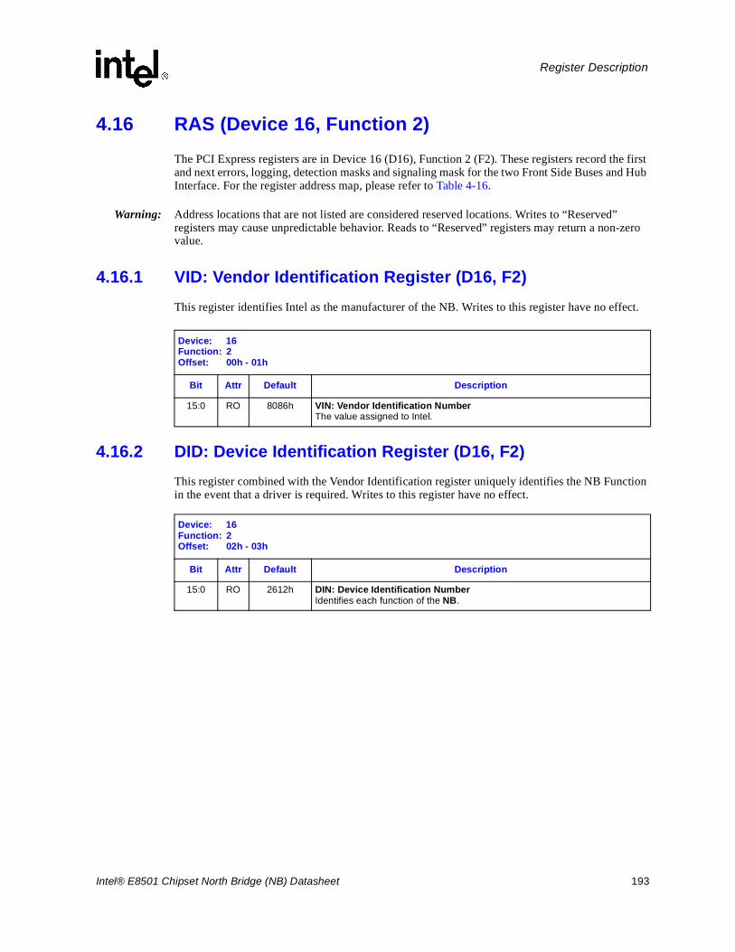
Intel® E8501 Chipset North Bridge (NB) Datasheet 193
Register Description
4.16 RAS (Device 16, Function 2)The PCI Express registers are in Device 16 (D16), Function 2 (F2). These registers record the first and next errors, logging, detection masks and signaling mask for the two Front Side Buses and Hub Interface. For the register address map, please refer to Table 4-16.
Warning: Address locations that are not listed are considered reserved locations. Writes to “Reserved” registers may cause unpredictable behavior. Reads to “Reserved” registers may return a non-zero value.
4.16.1 VID: Vendor Identification Register (D16, F2)This register identifies Intel as the manufacturer of the NB. Writes to this register have no effect.
4.16.2 DID: Device Identification Register (D16, F2)This register combined with the Vendor Identification register uniquely identifies the NB Function in the event that a driver is required. Writes to this register have no effect.
Device: 16Function: 2Offset: 00h - 01h
Bit Attr Default Description
15:0 RO 8086h VIN: Vendor Identification NumberThe value assigned to Intel.
Device: 16Function: 2Offset: 02h - 03h
Bit Attr Default Description
15:0 RO 2612h DIN: Device Identification Number Identifies each function of the NB.
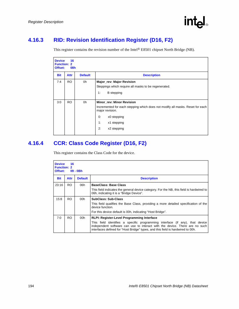
194 Intel® E8501 Chipset North Bridge (NB) Datasheet
Register Description
4.16.3 RID: Revision Identification Register (D16, F2)This register contains the revision number of the Intel® E8501 chipset North Bridge (NB).
4.16.4 CCR: Class Code Register (D16, F2)This register contains the Class Code for the device.
Device 16Function: 2Offset: 08h
Bit Attr Default Description
7:4 RO 0h Major_rev: Major RevisionSteppings which require all masks to be regenerated.
3:0 RO 0h Minor_rev: Minor RevisionIncremented for each stepping which does not modify all masks. Reset for eachmajor revision.
1: B stepping
0: x0 stepping
1: x1 stepping
2: x2 stepping
Device 16Function: 2Offset: 09 - 0Bh
Bit Attr Default Description
23:16 RO 06h BaseClass: Base ClassThis field indicates the general device category. For the NB, this field is hardwired to06h, indicating it is a “Bridge Device”.
15:8 RO 00h SubClass: Sub-ClassThis field qualifies the Base Class, providing a more detailed specification of thedevice function. For this device default is 00h, indicating “Host Bridge”.
7:0 RO 00h RLPI: Register-Level Programming InterfaceThis field identifies a specific programming interface (if any), that deviceindependent software can use to interact with the device. There are no suchinterfaces defined for “Host Bridge” types, and this field is hardwired to 00h.
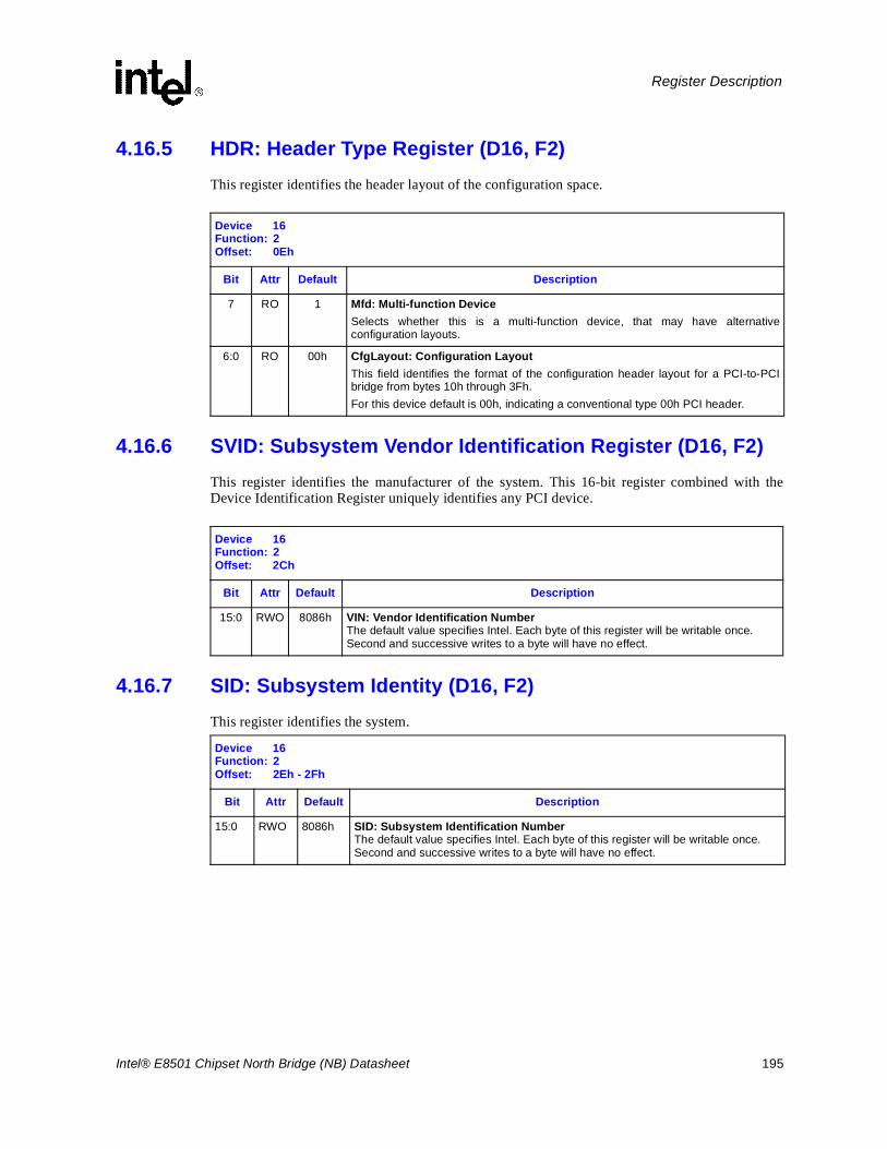
Intel® E8501 Chipset North Bridge (NB) Datasheet 195
Register Description
4.16.5 HDR: Header Type Register (D16, F2)This register identifies the header layout of the configuration space.
4.16.6 SVID: Subsystem Vendor Identification Register (D16, F2)This register identifies the manufacturer of the system. This 16-bit register combined with theDevice Identification Register uniquely identifies any PCI device.
4.16.7 SID: Subsystem Identity (D16, F2)This register identifies the system.
Device 16Function: 2Offset: 0Eh
Bit Attr Default Description
7 RO 1 Mfd: Multi-function DeviceSelects whether this is a multi-function device, that may have alternativeconfiguration layouts.
6:0 RO 00h CfgLayout: Configuration LayoutThis field identifies the format of the configuration header layout for a PCI-to-PCIbridge from bytes 10h through 3Fh. For this device default is 00h, indicating a conventional type 00h PCI header.
Device 16Function: 2Offset: 2Ch
Bit Attr Default Description
15:0 RWO 8086h VIN: Vendor Identification NumberThe default value specifies Intel. Each byte of this register will be writable once. Second and successive writes to a byte will have no effect.
Device 16Function: 2Offset: 2Eh - 2Fh
Bit Attr Default Description
15:0 RWO 8086h SID: Subsystem Identification Number The default value specifies Intel. Each byte of this register will be writable once. Second and successive writes to a byte will have no effect.
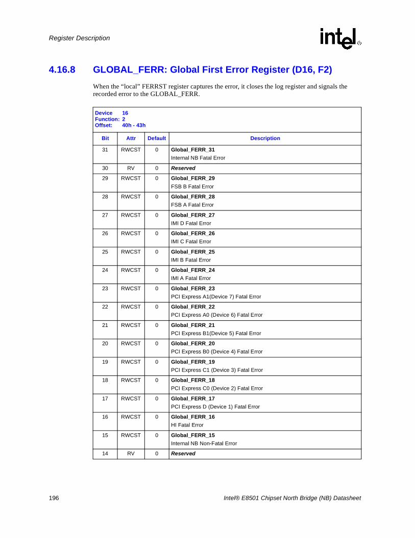
196 Intel® E8501 Chipset North Bridge (NB) Datasheet
Register Description
4.16.8 GLOBAL_FERR: Global First Error Register (D16, F2)When the “local” FERRST register captures the error, it closes the log register and signals the recorded error to the GLOBAL_FERR.
Device 16Function: 2Offset: 40h - 43h
Bit Attr Default Description
31 RWCST 0 Global_FERR_31Internal NB Fatal Error
30 RV 0 Reserved
29 RWCST 0 Global_FERR_29FSB B Fatal Error
28 RWCST 0 Global_FERR_28FSB A Fatal Error
27 RWCST 0 Global_FERR_27IMI D Fatal Error
26 RWCST 0 Global_FERR_26IMI C Fatal Error
25 RWCST 0 Global_FERR_25IMI B Fatal Error
24 RWCST 0 Global_FERR_24IMI A Fatal Error
23 RWCST 0 Global_FERR_23PCI Express A1(Device 7) Fatal Error
22 RWCST 0 Global_FERR_22PCI Express A0 (Device 6) Fatal Error
21 RWCST 0 Global_FERR_21PCI Express B1(Device 5) Fatal Error
20 RWCST 0 Global_FERR_20PCI Express B0 (Device 4) Fatal Error
19 RWCST 0 Global_FERR_19PCI Express C1 (Device 3) Fatal Error
18 RWCST 0 Global_FERR_18PCI Express C0 (Device 2) Fatal Error
17 RWCST 0 Global_FERR_17PCI Express D (Device 1) Fatal Error
16 RWCST 0 Global_FERR_16HI Fatal Error
15 RWCST 0 Global_FERR_15Internal NB Non-Fatal Error
14 RV 0 Reserved
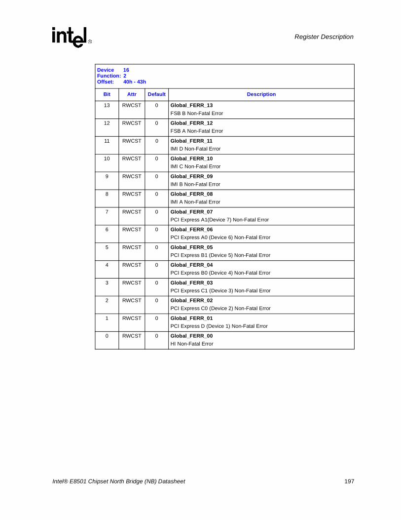
Intel® E8501 Chipset North Bridge (NB) Datasheet 197
Register Description
13 RWCST 0 Global_FERR_13FSB B Non-Fatal Error
12 RWCST 0 Global_FERR_12FSB A Non-Fatal Error
11 RWCST 0 Global_FERR_11IMI D Non-Fatal Error
10 RWCST 0 Global_FERR_10IMI C Non-Fatal Error
9 RWCST 0 Global_FERR_09IMI B Non-Fatal Error
8 RWCST 0 Global_FERR_08IMI A Non-Fatal Error
7 RWCST 0 Global_FERR_07PCI Express A1(Device 7) Non-Fatal Error
6 RWCST 0 Global_FERR_06PCI Express A0 (Device 6) Non-Fatal Error
5 RWCST 0 Global_FERR_05PCI Express B1 (Device 5) Non-Fatal Error
4 RWCST 0 Global_FERR_04PCI Express B0 (Device 4) Non-Fatal Error
3 RWCST 0 Global_FERR_03PCI Express C1 (Device 3) Non-Fatal Error
2 RWCST 0 Global_FERR_02PCI Express C0 (Device 2) Non-Fatal Error
1 RWCST 0 Global_FERR_01PCI Express D (Device 1) Non-Fatal Error
0 RWCST 0 Global_FERR_00HI Non-Fatal Error
Device 16Function: 2Offset: 40h - 43h
Bit Attr Default Description
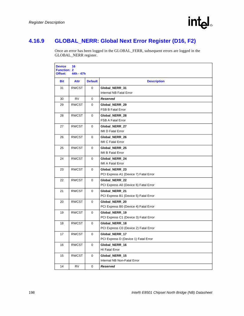
198 Intel® E8501 Chipset North Bridge (NB) Datasheet
Register Description
4.16.9 GLOBAL_NERR: Global Next Error Register (D16, F2)Once an error has been logged in the GLOBAL_FERR, subsequent errors are logged in the GLOBAL_NERR register.
Device 16Function: 2Offset: 44h - 47h
Bit Attr Default Description
31 RWCST 0 Global_NERR_31Internal NB Fatal Error
30 RV 0 Reserved
29 RWCST 0 Global_NERR_29FSB B Fatal Error
28 RWCST 0 Global_NERR_28FSB A Fatal Error
27 RWCST 0 Global_NERR_27IMI D Fatal Error
26 RWCST 0 Global_NERR_26IMI C Fatal Error
25 RWCST 0 Global_NERR_25IMI B Fatal Error
24 RWCST 0 Global_NERR_24IMI A Fatal Error
23 RWCST 0 Global_NERR_23PCI Express A1 (Device 7) Fatal Error
22 RWCST 0 Global_NERR_22PCI Express A0 (Device 6) Fatal Error
21 RWCST 0 Global_NERR_21PCI Express B1 (Device 5) Fatal Error
20 RWCST 0 Global_NERR_20PCI Express B0 (Device 4) Fatal Error
19 RWCST 0 Global_NERR_19PCI Express C1 (Device 3) Fatal Error
18 RWCST 0 Global_NERR_18PCI Express C0 (Device 2) Fatal Error
17 RWCST 0 Global_NERR_17PCI Express D (Device 1) Fatal Error
16 RWCST 0 Global_NERR_16HI Fatal Error
15 RWCST 0 Global_NERR_15Internal NB Non-Fatal Error
14 RV 0 Reserved
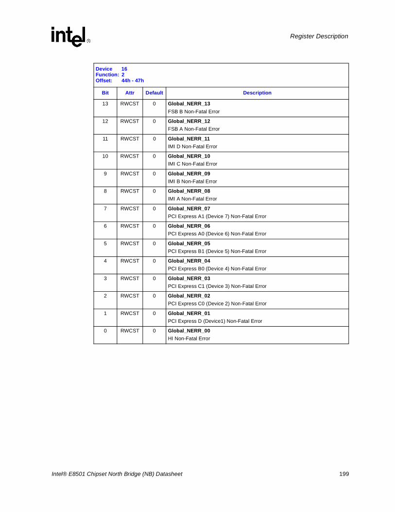
Intel® E8501 Chipset North Bridge (NB) Datasheet 199
Register Description
13 RWCST 0 Global_NERR_13FSB B Non-Fatal Error
12 RWCST 0 Global_NERR_12FSB A Non-Fatal Error
11 RWCST 0 Global_NERR_11IMI D Non-Fatal Error
10 RWCST 0 Global_NERR_10IMI C Non-Fatal Error
9 RWCST 0 Global_NERR_09IMI B Non-Fatal Error
8 RWCST 0 Global_NERR_08IMI A Non-Fatal Error
7 RWCST 0 Global_NERR_07PCI Express A1 (Device 7) Non-Fatal Error
6 RWCST 0 Global_NERR_06PCI Express A0 (Device 6) Non-Fatal Error
5 RWCST 0 Global_NERR_05PCI Express B1 (Device 5) Non-Fatal Error
4 RWCST 0 Global_NERR_04PCI Express B0 (Device 4) Non-Fatal Error
3 RWCST 0 Global_NERR_03PCI Express C1 (Device 3) Non-Fatal Error
2 RWCST 0 Global_NERR_02PCI Express C0 (Device 2) Non-Fatal Error
1 RWCST 0 Global_NERR_01PCI Express D (Device1) Non-Fatal Error
0 RWCST 0 Global_NERR_00HI Non-Fatal Error
Device 16Function: 2Offset: 44h - 47h
Bit Attr Default Description
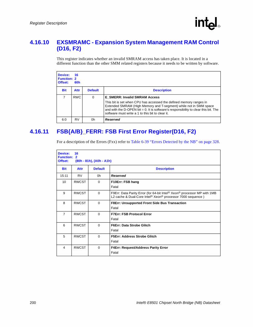
200 Intel® E8501 Chipset North Bridge (NB) Datasheet
Register Description
4.16.10 EXSMRAMC - Expansion System Management RAM Control (D16, F2)This register indicates whether an invalid SMRAM access has taken place. It is located in a different function than the other SMM related registers because it needs to be written by software.
4.16.11 FSB{A/B}_FERR: FSB First Error Register(D16, F2)For a description of the Errors (Fxx) refer to Table 6-39 “Errors Detected by the NB” on page 328.
Device: 16Function: 2Offset: 60h
Bit Attr Default Description
7 RWC 0 E_SMERR: Invalid SMRAM AccessThis bit is set when CPU has accessed the defined memory ranges in Extended SMRAM (High Memory and T-segment) while not in SMM space and with the D-OPEN bit = 0. It is software's responsibility to clear this bit. The software must write a 1 to this bit to clear it.
6:0 RV 0h Reserved
Device: 16Function: 2Offset: (80h - 81h), (A0h - A1h)
Bit Attr Default Description
15:11 RV 0h Reserved
10 RWCST 0 F10Err: FSB hangFatal
9 RWCST 0 F9Err: Data Parity Error (for 64-bit Intel® Xeon® processor MP with 1MB L2 cache & Dual-Core Intel® Xeon® processor 7000 sequence )
8 RWCST 0 F8Err: Unsupported Front Side Bus TransactionFatal
7 RWCST 0 F7Err: FSB Protocol ErrorFatal
6 RWCST 0 F6Err: Data Strobe GlitchFatal
5 RWCST 0 F5Err: Address Strobe GlitchFatal
4 RWCST 0 F4Err: Request/Address Parity ErrorFatal
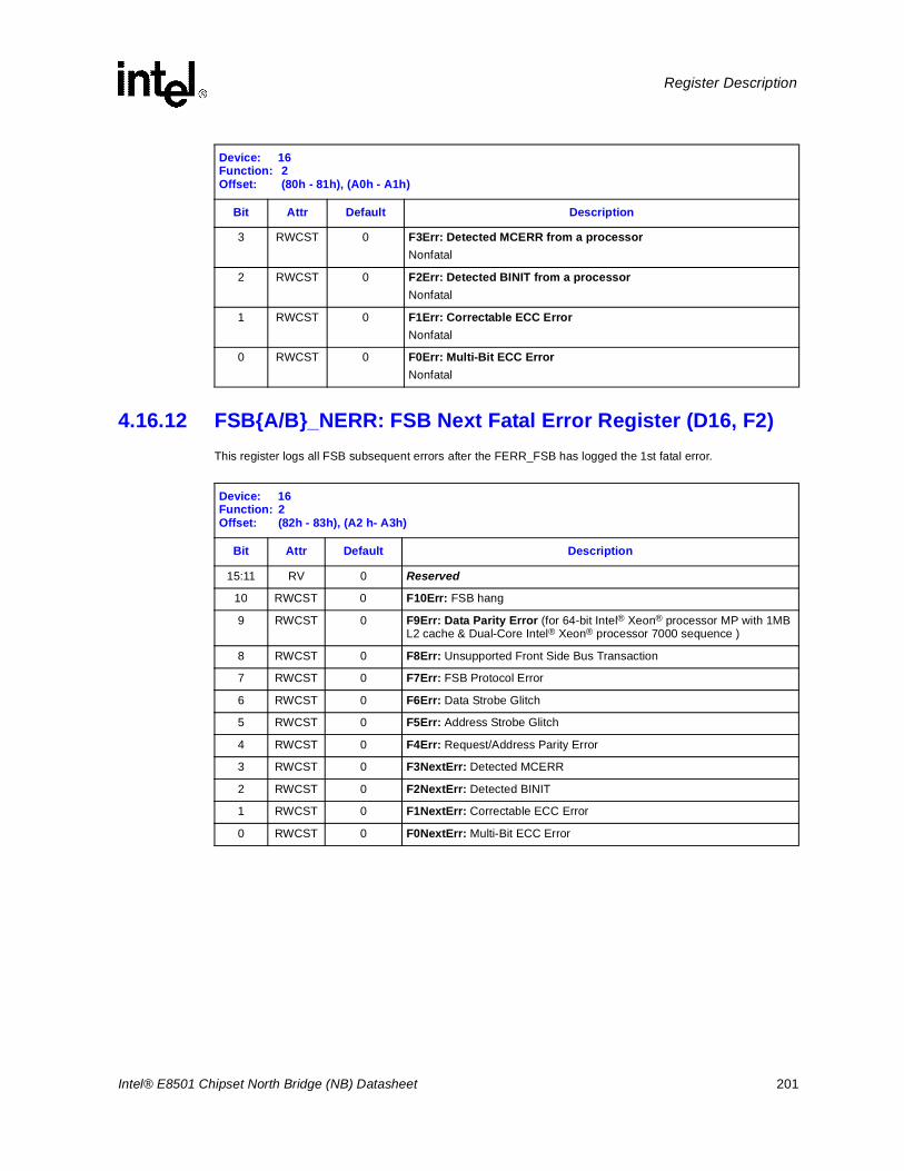
Intel® E8501 Chipset North Bridge (NB) Datasheet 201
Register Description
4.16.12 FSB{A/B}_NERR: FSB Next Fatal Error Register (D16, F2)This register logs all FSB subsequent errors after the FERR_FSB has logged the 1st fatal error.
3 RWCST 0 F3Err: Detected MCERR from a processorNonfatal
2 RWCST 0 F2Err: Detected BINIT from a processorNonfatal
1 RWCST 0 F1Err: Correctable ECC ErrorNonfatal
0 RWCST 0 F0Err: Multi-Bit ECC ErrorNonfatal
Device: 16Function: 2Offset: (80h - 81h), (A0h - A1h)
Bit Attr Default Description
Device: 16Function: 2Offset: (82h - 83h), (A2 h- A3h)
Bit Attr Default Description
15:11 RV 0 Reserved
10 RWCST 0 F10Err: FSB hang
9 RWCST 0 F9Err: Data Parity Error (for 64-bit Intel® Xeon® processor MP with 1MB L2 cache & Dual-Core Intel® Xeon® processor 7000 sequence )
8 RWCST 0 F8Err: Unsupported Front Side Bus Transaction
7 RWCST 0 F7Err: FSB Protocol Error
6 RWCST 0 F6Err: Data Strobe Glitch
5 RWCST 0 F5Err: Address Strobe Glitch
4 RWCST 0 F4Err: Request/Address Parity Error
3 RWCST 0 F3NextErr: Detected MCERR
2 RWCST 0 F2NextErr: Detected BINIT
1 RWCST 0 F1NextErr: Correctable ECC Error
0 RWCST 0 F0NextErr: Multi-Bit ECC Error
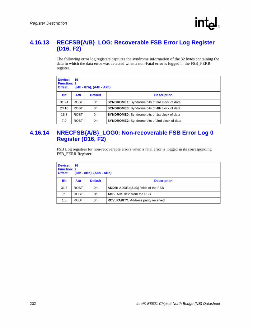
202 Intel® E8501 Chipset North Bridge (NB) Datasheet
Register Description
4.16.13 RECFSB{A/B}_LOG: Recoverable FSB Error Log Register(D16, F2)The following error log registers captures the syndrome information of the 32 bytes containing the data in which the data error was detected when a non-Fatal error is logged in the FSB_FERR register.
4.16.14 NRECFSB{A/B}_LOG0: Non-recoverable FSB Error Log 0 Register (D16, F2)FSB Log registers for non-recoverable errors when a fatal error is logged in its corresponding FSB_FERR Register.
Device: 16Function: 2Offset: (84h - 87h), (A4h - A7h)
Bit Attr Default Description
31:24 ROST 0h SYNDROME1: Syndrome bits of 3rd clock of data
23:16 ROST 0h SYNDROME3: Syndrome bits of 4th clock of data
15:8 ROST 0h SYNDROME0: Syndrome bits of 1st clock of data
7:0 ROST 0h SYNDROME2: Syndrome bits of 2nd clock of data
Device: 16Function: 2Offset: (88h - 8Bh), (A8h - ABh)
Bit Attr Default Description
31:3 ROST 0h ADDR: ADDRa[31:3] fields of the FSB
2 ROST 0h ADS: ADS field from the FSB
1:0 ROST 0h RCV_PARITY: Address parity received
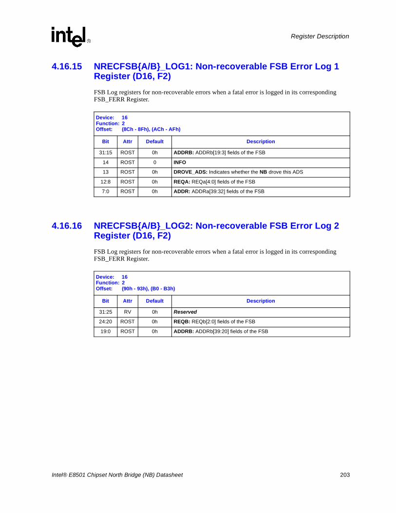
Intel® E8501 Chipset North Bridge (NB) Datasheet 203
Register Description
4.16.15 NRECFSB{A/B}_LOG1: Non-recoverable FSB Error Log 1Register (D16, F2)FSB Log registers for non-recoverable errors when a fatal error is logged in its corresponding FSB_FERR Register.
4.16.16 NRECFSB{A/B}_LOG2: Non-recoverable FSB Error Log 2Register (D16, F2)FSB Log registers for non-recoverable errors when a fatal error is logged in its corresponding FSB_FERR Register.
Device: 16Function: 2Offset: (8Ch - 8Fh), (ACh - AFh)
Bit Attr Default Description
31:15 ROST 0h ADDRB: ADDRb[19:3] fields of the FSB
14 ROST 0 INFO
13 ROST 0h DROVE_ADS: Indicates whether the NB drove this ADS
12:8 ROST 0h REQA: REQa[4:0] fields of the FSB
7:0 ROST 0h ADDR: ADDRa[39:32] fields of the FSB
Device: 16Function: 2Offset: (90h - 93h), (B0 - B3h)
Bit Attr Default Description
31:25 RV 0h Reserved
24:20 ROST 0h REQB: REQb[2:0] fields of the FSB
19:0 ROST 0h ADDRB: ADDRb[39:20] fields of the FSB
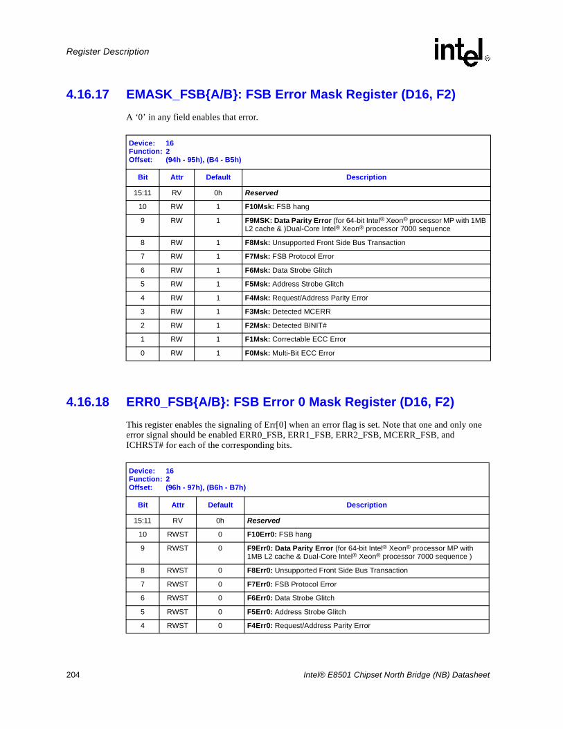
204 Intel® E8501 Chipset North Bridge (NB) Datasheet
Register Description
4.16.17 EMASK_FSB{A/B}: FSB Error Mask Register (D16, F2)A ‘0’ in any field enables that error.
4.16.18 ERR0_FSB{A/B}: FSB Error 0 Mask Register (D16, F2)This register enables the signaling of Err[0] when an error flag is set. Note that one and only one error signal should be enabled ERR0_FSB, ERR1_FSB, ERR2_FSB, MCERR_FSB, and ICHRST# for each of the corresponding bits.
Device: 16Function: 2Offset: (94h - 95h), (B4 - B5h)
Bit Attr Default Description
15:11 RV 0h Reserved
10 RW 1 F10Msk: FSB hang
9 RW 1 F9MSK: Data Parity Error (for 64-bit Intel® Xeon® processor MP with 1MB L2 cache & )Dual-Core Intel® Xeon® processor 7000 sequence
8 RW 1 F8Msk: Unsupported Front Side Bus Transaction
7 RW 1 F7Msk: FSB Protocol Error
6 RW 1 F6Msk: Data Strobe Glitch
5 RW 1 F5Msk: Address Strobe Glitch
4 RW 1 F4Msk: Request/Address Parity Error
3 RW 1 F3Msk: Detected MCERR
2 RW 1 F2Msk: Detected BINIT#
1 RW 1 F1Msk: Correctable ECC Error
0 RW 1 F0Msk: Multi-Bit ECC Error
Device: 16Function: 2Offset: (96h - 97h), (B6h - B7h)
Bit Attr Default Description
15:11 RV 0h Reserved
10 RWST 0 F10Err0: FSB hang
9 RWST 0 F9Err0: Data Parity Error (for 64-bit Intel® Xeon® processor MP with 1MB L2 cache & Dual-Core Intel® Xeon® processor 7000 sequence )
8 RWST 0 F8Err0: Unsupported Front Side Bus Transaction
7 RWST 0 F7Err0: FSB Protocol Error
6 RWST 0 F6Err0: Data Strobe Glitch
5 RWST 0 F5Err0: Address Strobe Glitch
4 RWST 0 F4Err0: Request/Address Parity Error
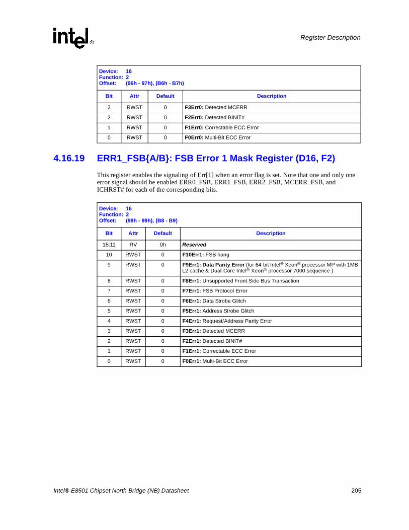
Intel® E8501 Chipset North Bridge (NB) Datasheet 205
Register Description
4.16.19 ERR1_FSB{A/B}: FSB Error 1 Mask Register (D16, F2)This register enables the signaling of Err[1] when an error flag is set. Note that one and only one error signal should be enabled ERR0_FSB, ERR1_FSB, ERR2_FSB, MCERR_FSB, and ICHRST# for each of the corresponding bits.
3 RWST 0 F3Err0: Detected MCERR
2 RWST 0 F2Err0: Detected BINIT#
1 RWST 0 F1Err0: Correctable ECC Error
0 RWST 0 F0Err0: Multi-Bit ECC Error
Device: 16Function: 2Offset: (96h - 97h), (B6h - B7h)
Bit Attr Default Description
Device: 16Function: 2Offset: (98h - 99h), (B8 - B9)
Bit Attr Default Description
15:11 RV 0h Reserved
10 RWST 0 F10Err1: FSB hang
9 RWST 0 F9Err1: Data Parity Error (for 64-bit Intel® Xeon® processor MP with 1MB L2 cache & Dual-Core Intel® Xeon® processor 7000 sequence )
8 RWST 0 F8Err1: Unsupported Front Side Bus Transaction
7 RWST 0 F7Err1: FSB Protocol Error
6 RWST 0 F6Err1: Data Strobe Glitch
5 RWST 0 F5Err1: Address Strobe Glitch
4 RWST 0 F4Err1: Request/Address Parity Error
3 RWST 0 F3Err1: Detected MCERR
2 RWST 0 F2Err1: Detected BINIT#
1 RWST 0 F1Err1: Correctable ECC Error
0 RWST 0 F0Err1: Multi-Bit ECC Error
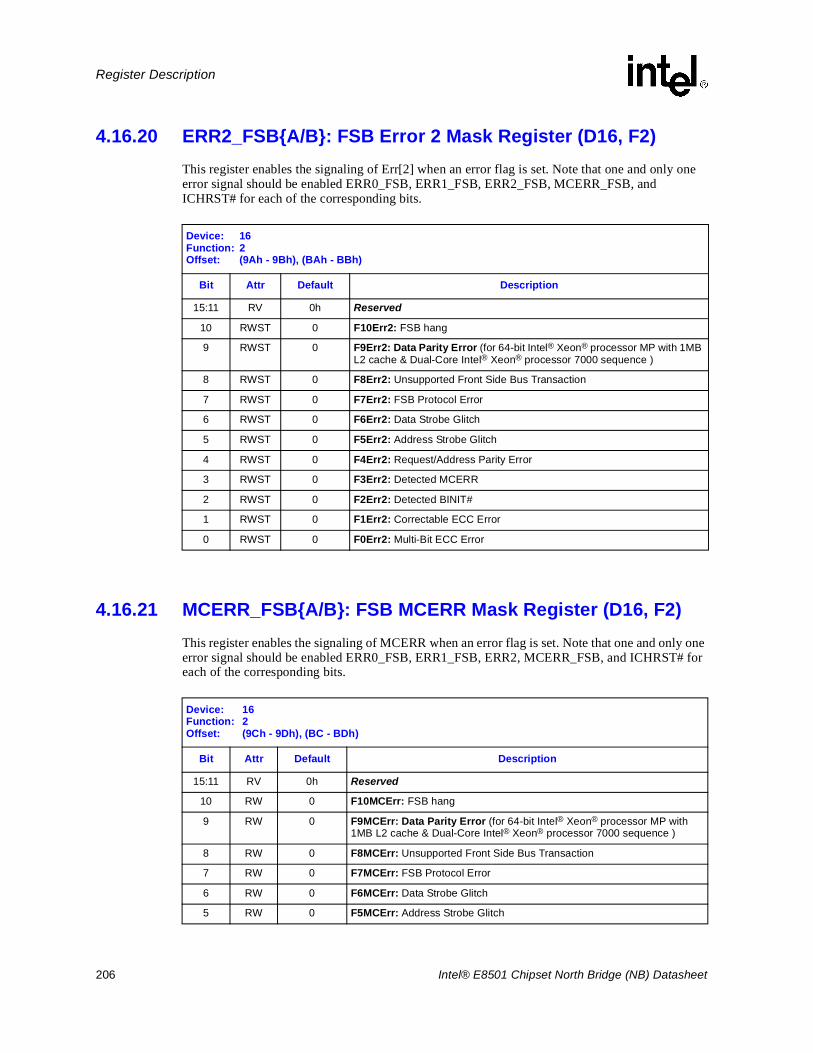
206 Intel® E8501 Chipset North Bridge (NB) Datasheet
Register Description
4.16.20 ERR2_FSB{A/B}: FSB Error 2 Mask Register (D16, F2)This register enables the signaling of Err[2] when an error flag is set. Note that one and only one error signal should be enabled ERR0_FSB, ERR1_FSB, ERR2_FSB, MCERR_FSB, and ICHRST# for each of the corresponding bits.
4.16.21 MCERR_FSB{A/B}: FSB MCERR Mask Register (D16, F2)This register enables the signaling of MCERR when an error flag is set. Note that one and only one error signal should be enabled ERR0_FSB, ERR1_FSB, ERR2, MCERR_FSB, and ICHRST# for each of the corresponding bits.
Device: 16Function: 2Offset: (9Ah - 9Bh), (BAh - BBh)
Bit Attr Default Description
15:11 RV 0h Reserved
10 RWST 0 F10Err2: FSB hang
9 RWST 0 F9Err2: Data Parity Error (for 64-bit Intel® Xeon® processor MP with 1MB L2 cache & Dual-Core Intel® Xeon® processor 7000 sequence )
8 RWST 0 F8Err2: Unsupported Front Side Bus Transaction
7 RWST 0 F7Err2: FSB Protocol Error
6 RWST 0 F6Err2: Data Strobe Glitch
5 RWST 0 F5Err2: Address Strobe Glitch
4 RWST 0 F4Err2: Request/Address Parity Error
3 RWST 0 F3Err2: Detected MCERR
2 RWST 0 F2Err2: Detected BINIT#
1 RWST 0 F1Err2: Correctable ECC Error
0 RWST 0 F0Err2: Multi-Bit ECC Error
Device: 16Function: 2Offset: (9Ch - 9Dh), (BC - BDh)
Bit Attr Default Description
15:11 RV 0h Reserved
10 RW 0 F10MCErr: FSB hang
9 RW 0 F9MCErr: Data Parity Error (for 64-bit Intel® Xeon® processor MP with 1MB L2 cache & Dual-Core Intel® Xeon® processor 7000 sequence )
8 RW 0 F8MCErr: Unsupported Front Side Bus Transaction
7 RW 0 F7MCErr: FSB Protocol Error
6 RW 0 F6MCErr: Data Strobe Glitch
5 RW 0 F5MCErr: Address Strobe Glitch
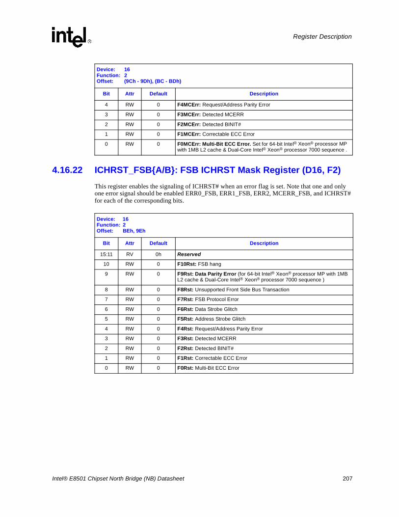
Intel® E8501 Chipset North Bridge (NB) Datasheet 207
Register Description
4.16.22 ICHRST_FSB{A/B}: FSB ICHRST Mask Register (D16, F2)This register enables the signaling of ICHRST# when an error flag is set. Note that one and only one error signal should be enabled ERR0_FSB, ERR1_FSB, ERR2, MCERR_FSB, and ICHRST# for each of the corresponding bits.
4 RW 0 F4MCErr: Request/Address Parity Error
3 RW 0 F3MCErr: Detected MCERR
2 RW 0 F2MCErr: Detected BINIT#
1 RW 0 F1MCErr: Correctable ECC Error
0 RW 0 F0MCErr: Multi-Bit ECC Error. Set for 64-bit Intel® Xeon® processor MP with 1MB L2 cache & Dual-Core Intel® Xeon® processor 7000 sequence .
Device: 16Function: 2Offset: (9Ch - 9Dh), (BC - BDh)
Bit Attr Default Description
Device: 16Function: 2Offset: BEh, 9Eh
Bit Attr Default Description
15:11 RV 0h Reserved
10 RW 0 F10Rst: FSB hang
9 RW 0 F9Rst: Data Parity Error (for 64-bit Intel® Xeon® processor MP with 1MB L2 cache & Dual-Core Intel® Xeon® processor 7000 sequence )
8 RW 0 F8Rst: Unsupported Front Side Bus Transaction
7 RW 0 F7Rst: FSB Protocol Error
6 RW 0 F6Rst: Data Strobe Glitch
5 RW 0 F5Rst: Address Strobe Glitch
4 RW 0 F4Rst: Request/Address Parity Error
3 RW 0 F3Rst: Detected MCERR
2 RW 0 F2Rst: Detected BINIT#
1 RW 0 F1Rst: Correctable ECC Error
0 RW 0 F0Rst: Multi-Bit ECC Error
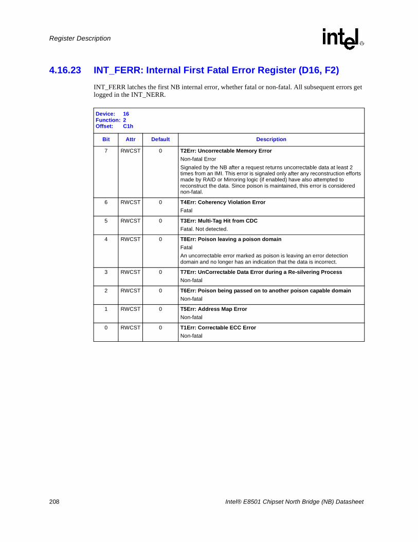
208 Intel® E8501 Chipset North Bridge (NB) Datasheet
Register Description
4.16.23 INT_FERR: Internal First Fatal Error Register (D16, F2)INT_FERR latches the first NB internal error, whether fatal or non-fatal. All subsequent errors get logged in the INT_NERR.
Device: 16Function: 2Offset: C1h
Bit Attr Default Description
7 RWCST 0 T2Err: Uncorrectable Memory ErrorNon-fatal ErrorSignaled by the NB after a request returns uncorrectable data at least 2 times from an IMI. This error is signaled only after any reconstruction efforts made by RAID or Mirroring logic (if enabled) have also attempted to reconstruct the data. Since poison is maintained, this error is considered non-fatal.
6 RWCST 0 T4Err: Coherency Violation ErrorFatal
5 RWCST 0 T3Err: Multi-Tag Hit from CDCFatal. Not detected.
4 RWCST 0 T8Err: Poison leaving a poison domainFatalAn uncorrectable error marked as poison is leaving an error detection domain and no longer has an indication that the data is incorrect.
3 RWCST 0 T7Err: UnCorrectable Data Error during a Re-silvering ProcessNon-fatal
2 RWCST 0 T6Err: Poison being passed on to another poison capable domainNon-fatal
1 RWCST 0 T5Err: Address Map ErrorNon-fatal
0 RWCST 0 T1Err: Correctable ECC ErrorNon-fatal
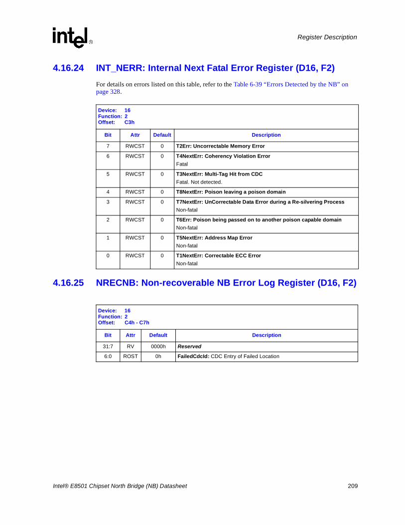
Intel® E8501 Chipset North Bridge (NB) Datasheet 209
Register Description
4.16.24 INT_NERR: Internal Next Fatal Error Register (D16, F2)For details on errors listed on this table, refer to the Table 6-39 “Errors Detected by the NB” on page 328.
4.16.25 NRECNB: Non-recoverable NB Error Log Register (D16, F2)
Device: 16Function: 2Offset: C3h
Bit Attr Default Description
7 RWCST 0 T2Err: Uncorrectable Memory Error
6 RWCST 0 T4NextErr: Coherency Violation ErrorFatal
5 RWCST 0 T3NextErr: Multi-Tag Hit from CDCFatal. Not detected.
4 RWCST 0 T8NextErr: Poison leaving a poison domain
3 RWCST 0 T7NextErr: UnCorrectable Data Error during a Re-silvering ProcessNon-fatal
2 RWCST 0 T6Err: Poison being passed on to another poison capable domainNon-fatal
1 RWCST 0 T5NextErr: Address Map ErrorNon-fatal
0 RWCST 0 T1NextErr: Correctable ECC ErrorNon-fatal
Device: 16Function: 2Offset: C4h - C7h
Bit Attr Default Description
31:7 RV 0000h Reserved
6:0 ROST 0h FailedCdcId: CDC Entry of Failed Location
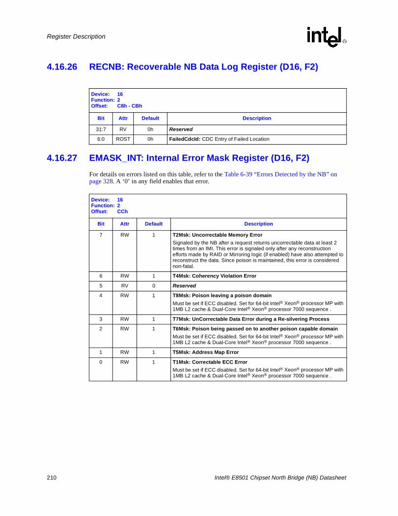
210 Intel® E8501 Chipset North Bridge (NB) Datasheet
Register Description
4.16.26 RECNB: Recoverable NB Data Log Register (D16, F2)
4.16.27 EMASK_INT: Internal Error Mask Register (D16, F2)For details on errors listed on this table, refer to the Table 6-39 “Errors Detected by the NB” on page 328. A ‘0’ in any field enables that error.
Device: 16Function: 2Offset: C8h - CBh
Bit Attr Default Description
31:7 RV 0h Reserved
6:0 ROST 0h FailedCdcId: CDC Entry of Failed Location
Device: 16Function: 2Offset: CCh
Bit Attr Default Description
7 RW 1 T2Msk: Uncorrectable Memory ErrorSignaled by the NB after a request returns uncorrectable data at least 2 times from an IMI. This error is signaled only after any reconstruction efforts made by RAID or Mirroring logic (if enabled) have also attempted to reconstruct the data. Since poison is maintained, this error is considered non-fatal.
6 RW 1 T4Msk: Coherency Violation Error
5 RV 0 Reserved
4 RW 1 T8Msk: Poison leaving a poison domainMust be set if ECC disabled. Set for 64-bit Intel® Xeon® processor MP with 1MB L2 cache & Dual-Core Intel® Xeon® processor 7000 sequence .
3 RW 1 T7Msk: UnCorrectable Data Error during a Re-silvering Process
2 RW 1 T6Msk: Poison being passed on to another poison capable domainMust be set if ECC disabled. Set for 64-bit Intel® Xeon® processor MP with 1MB L2 cache & Dual-Core Intel® Xeon® processor 7000 sequence .
1 RW 1 T5Msk: Address Map Error
0 RW 1 T1Msk: Correctable ECC ErrorMust be set if ECC disabled. Set for 64-bit Intel® Xeon® processor MP with 1MB L2 cache & Dual-Core Intel® Xeon® processor 7000 sequence .
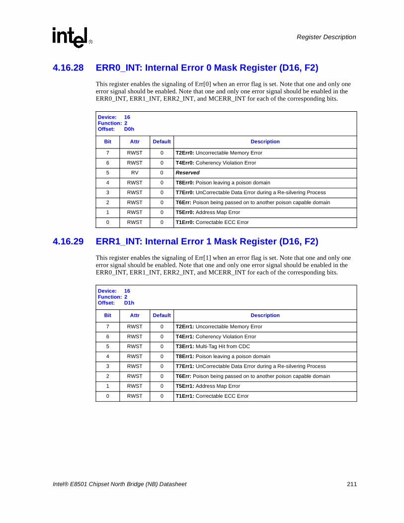
Intel® E8501 Chipset North Bridge (NB) Datasheet 211
Register Description
4.16.28 ERR0_INT: Internal Error 0 Mask Register (D16, F2)This register enables the signaling of Err[0] when an error flag is set. Note that one and only one error signal should be enabled. Note that one and only one error signal should be enabled in the ERR0_INT, ERR1_INT, ERR2_INT, and MCERR_INT for each of the corresponding bits.
4.16.29 ERR1_INT: Internal Error 1 Mask Register (D16, F2)This register enables the signaling of Err[1] when an error flag is set. Note that one and only one error signal should be enabled. Note that one and only one error signal should be enabled in the ERR0_INT, ERR1_INT, ERR2_INT, and MCERR_INT for each of the corresponding bits.
Device: 16Function: 2Offset: D0h
Bit Attr Default Description
7 RWST 0 T2Err0: Uncorrectable Memory Error
6 RWST 0 T4Err0: Coherency Violation Error
5 RV 0 Reserved
4 RWST 0 T8Err0: Poison leaving a poison domain
3 RWST 0 T7Err0: UnCorrectable Data Error during a Re-silvering Process
2 RWST 0 T6Err: Poison being passed on to another poison capable domain
1 RWST 0 T5Err0: Address Map Error
0 RWST 0 T1Err0: Correctable ECC Error
Device: 16Function: 2Offset: D1h
Bit Attr Default Description
7 RWST 0 T2Err1: Uncorrectable Memory Error
6 RWST 0 T4Err1: Coherency Violation Error
5 RWST 0 T3Err1: Multi-Tag Hit from CDC
4 RWST 0 T8Err1: Poison leaving a poison domain
3 RWST 0 T7Err1: UnCorrectable Data Error during a Re-silvering Process
2 RWST 0 T6Err: Poison being passed on to another poison capable domain
1 RWST 0 T5Err1: Address Map Error
0 RWST 0 T1Err1: Correctable ECC Error
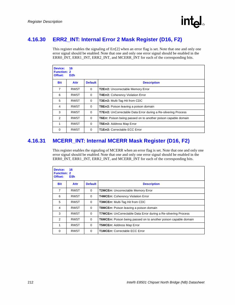
212 Intel® E8501 Chipset North Bridge (NB) Datasheet
Register Description
4.16.30 ERR2_INT: Internal Error 2 Mask Register (D16, F2)This register enables the signaling of Err[2] when an error flag is set. Note that one and only one error signal should be enabled. Note that one and only one error signal should be enabled in the ERR0_INT, ERR1_INT, ERR2_INT, and MCERR_INT for each of the corresponding bits.
4.16.31 MCERR_INT: Internal MCERR Mask Register (D16, F2)This register enables the signaling of MCERR when an error flag is set. Note that one and only one error signal should be enabled. Note that one and only one error signal should be enabled in the ERR0_INT, ERR1_INT, ERR2_INT, and MCERR_INT for each of the corresponding bits.
Device: 16Function: 2Offset: D2h
Bit Attr Default Description
7 RWST 0 T2Err2: Uncorrectable Memory Error
6 RWST 0 T4Err2: Coherency Violation Error
5 RWST 0 T3Err2: Multi-Tag Hit from CDC
4 RWST 0 T8Err2: Poison leaving a poison domain
3 RWST 0 T7Err2: UnCorrectable Data Error during a Re-silvering Process
2 RWST 0 T6Err: Poison being passed on to another poison capable domain
1 RWST 0 T5Err2: Address Map Error
0 RWST 0 T1Err2: Correctable ECC Error
Device: 16Function: 2Offset: D3h
Bit Attr Default Description
7 RWST 0 T2MCErr: Uncorrectable Memory Error
6 RWST 0 T4MCErr: Coherency Violation Error
5 RWST 0 T3MCErr: Multi-Tag Hit from CDC
4 RWST 0 T8MCErr: Poison leaving a poison domain
3 RWST 0 T7MCErr: UnCorrectable Data Error during a Re-silvering Process
2 RWST 0 T6MCErr: Poison being passed on to another poison capable domain
1 RWST 0 T5MCErr: Address Map Error
0 RWST 0 T1MCErr: Correctable ECC Error
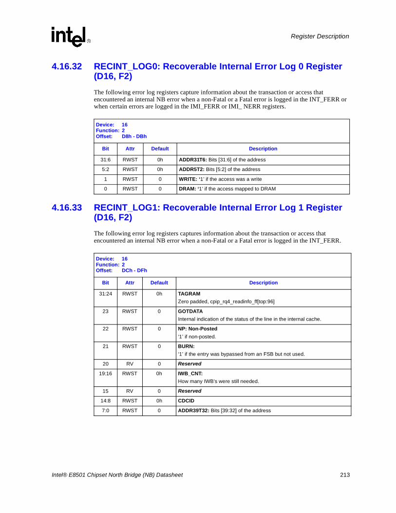
Intel® E8501 Chipset North Bridge (NB) Datasheet 213
Register Description
4.16.32 RECINT_LOG0: Recoverable Internal Error Log 0 Register(D16, F2)The following error log registers capture information about the transaction or access that encountered an internal NB error when a non-Fatal or a Fatal error is logged in the INT_FERR or when certain errors are logged in the IMI_FERR or IMI_ NERR registers.
4.16.33 RECINT_LOG1: Recoverable Internal Error Log 1 Register(D16, F2)The following error log registers captures information about the transaction or access that encountered an internal NB error when a non-Fatal or a Fatal error is logged in the INT_FERR.
Device: 16Function: 2Offset: D8h - DBh
Bit Attr Default Description
31:6 RWST 0h ADDR31T6: Bits [31:6] of the address
5:2 RWST 0h ADDR5T2: Bits [5:2] of the address
1 RWST 0 WRITE: ‘1’ if the access was a write
0 RWST 0 DRAM: ‘1’ if the access mapped to DRAM
Device: 16Function: 2Offset: DCh - DFh
Bit Attr Default Description
31:24 RWST 0h TAGRAMZero padded, cpip_rq4_readinfo_ff[top:96]
23 RWST 0 GOTDATAInternal indication of the status of the line in the internal cache.
22 RWST 0 NP: Non-Posted‘1’ if non-posted.
21 RWST 0 BURN: ‘1’ if the entry was bypassed from an FSB but not used.
20 RV 0 Reserved
19:16 RWST 0h IWB_CNT: How many IWB’s were still needed.
15 RV 0 Reserved
14:8 RWST 0h CDCID
7:0 RWST 0 ADDR39T32: Bits [39:32] of the address
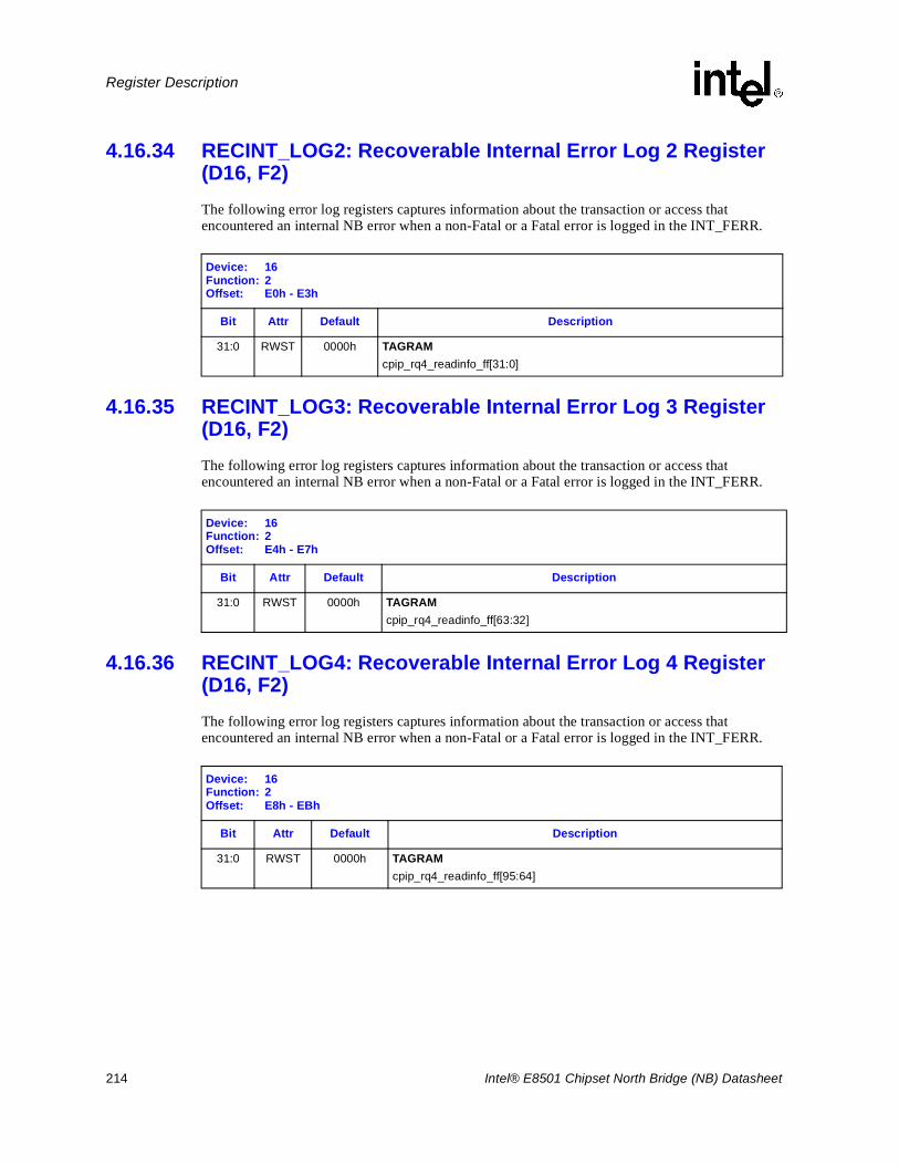
214 Intel® E8501 Chipset North Bridge (NB) Datasheet
Register Description
4.16.34 RECINT_LOG2: Recoverable Internal Error Log 2 Register(D16, F2)The following error log registers captures information about the transaction or access that encountered an internal NB error when a non-Fatal or a Fatal error is logged in the INT_FERR.
4.16.35 RECINT_LOG3: Recoverable Internal Error Log 3 Register(D16, F2)The following error log registers captures information about the transaction or access that encountered an internal NB error when a non-Fatal or a Fatal error is logged in the INT_FERR.
4.16.36 RECINT_LOG4: Recoverable Internal Error Log 4 Register(D16, F2)The following error log registers captures information about the transaction or access that encountered an internal NB error when a non-Fatal or a Fatal error is logged in the INT_FERR.
Device: 16Function: 2Offset: E0h - E3h
Bit Attr Default Description
31:0 RWST 0000h TAGRAMcpip_rq4_readinfo_ff[31:0]
Device: 16Function: 2Offset: E4h - E7h
Bit Attr Default Description
31:0 RWST 0000h TAGRAMcpip_rq4_readinfo_ff[63:32]
Device: 16Function: 2Offset: E8h - EBh
Bit Attr Default Description
31:0 RWST 0000h TAGRAM cpip_rq4_readinfo_ff[95:64]
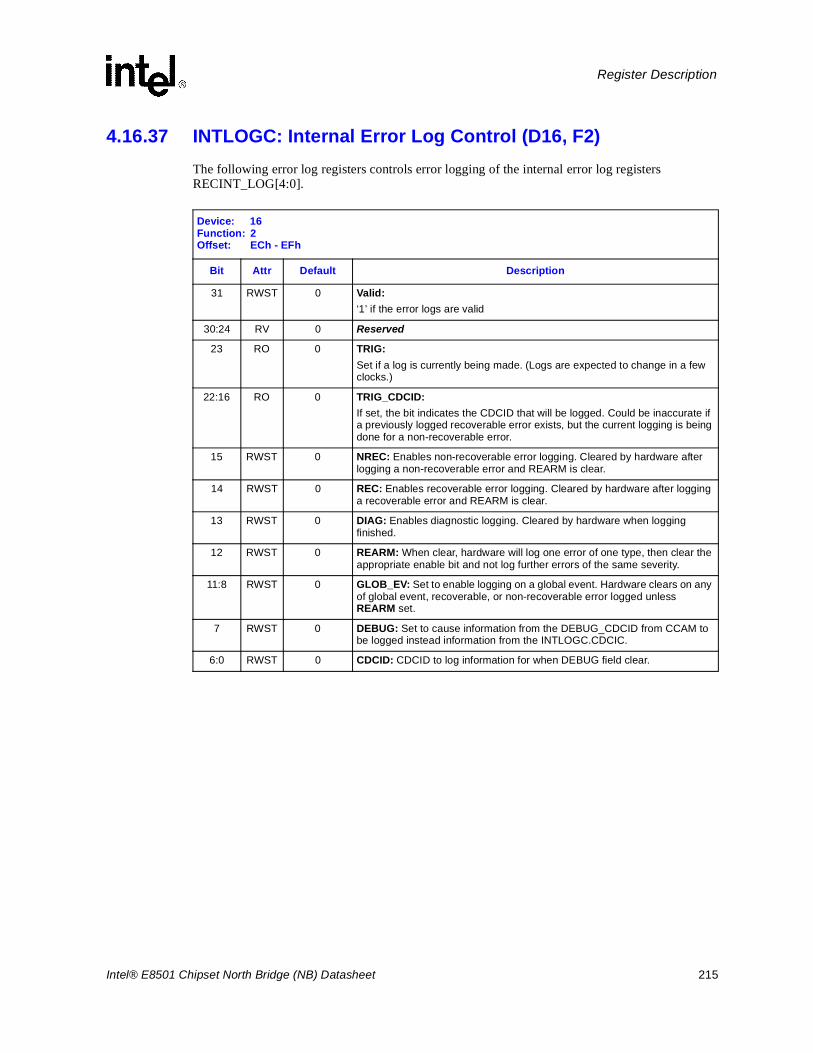
Intel® E8501 Chipset North Bridge (NB) Datasheet 215
Register Description
4.16.37 INTLOGC: Internal Error Log Control (D16, F2)The following error log registers controls error logging of the internal error log registers RECINT_LOG[4:0].
Device: 16Function: 2Offset: ECh - EFh
Bit Attr Default Description
31 RWST 0 Valid: ‘1’ if the error logs are valid
30:24 RV 0 Reserved
23 RO 0 TRIG: Set if a log is currently being made. (Logs are expected to change in a few clocks.)
22:16 RO 0 TRIG_CDCID:If set, the bit indicates the CDCID that will be logged. Could be inaccurate if a previously logged recoverable error exists, but the current logging is being done for a non-recoverable error.
15 RWST 0 NREC: Enables non-recoverable error logging. Cleared by hardware after logging a non-recoverable error and REARM is clear.
14 RWST 0 REC: Enables recoverable error logging. Cleared by hardware after logging a recoverable error and REARM is clear.
13 RWST 0 DIAG: Enables diagnostic logging. Cleared by hardware when logging finished.
12 RWST 0 REARM: When clear, hardware will log one error of one type, then clear the appropriate enable bit and not log further errors of the same severity.
11:8 RWST 0 GLOB_EV: Set to enable logging on a global event. Hardware clears on any of global event, recoverable, or non-recoverable error logged unless REARM set.
7 RWST 0 DEBUG: Set to cause information from the DEBUG_CDCID from CCAM to be logged instead information from the INTLOGC.CDCIC.
6:0 RWST 0 CDCID: CDCID to log information for when DEBUG field clear.
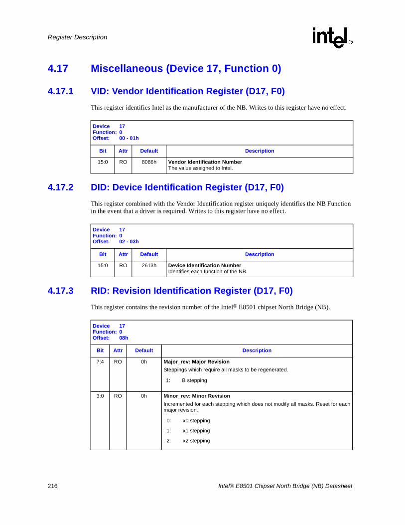
216 Intel® E8501 Chipset North Bridge (NB) Datasheet
Register Description
4.17 Miscellaneous (Device 17, Function 0)
4.17.1 VID: Vendor Identification Register (D17, F0)This register identifies Intel as the manufacturer of the NB. Writes to this register have no effect.
4.17.2 DID: Device Identification Register (D17, F0)This register combined with the Vendor Identification register uniquely identifies the NB Function in the event that a driver is required. Writes to this register have no effect.
4.17.3 RID: Revision Identification Register (D17, F0)This register contains the revision number of the Intel® E8501 chipset North Bridge (NB).
Device 17Function: 0Offset: 00 - 01h
Bit Attr Default Description
15:0 RO 8086h Vendor Identification NumberThe value assigned to Intel.
Device 17Function: 0Offset: 02 - 03h
Bit Attr Default Description
15:0 RO 2613h Device Identification NumberIdentifies each function of the NB.
Device 17Function: 0Offset: 08h
Bit Attr Default Description
7:4 RO 0h Major_rev: Major RevisionSteppings which require all masks to be regenerated.
3:0 RO 0h Minor_rev: Minor RevisionIncremented for each stepping which does not modify all masks. Reset for eachmajor revision.
1: B stepping
0: x0 stepping
1: x1 stepping
2: x2 stepping
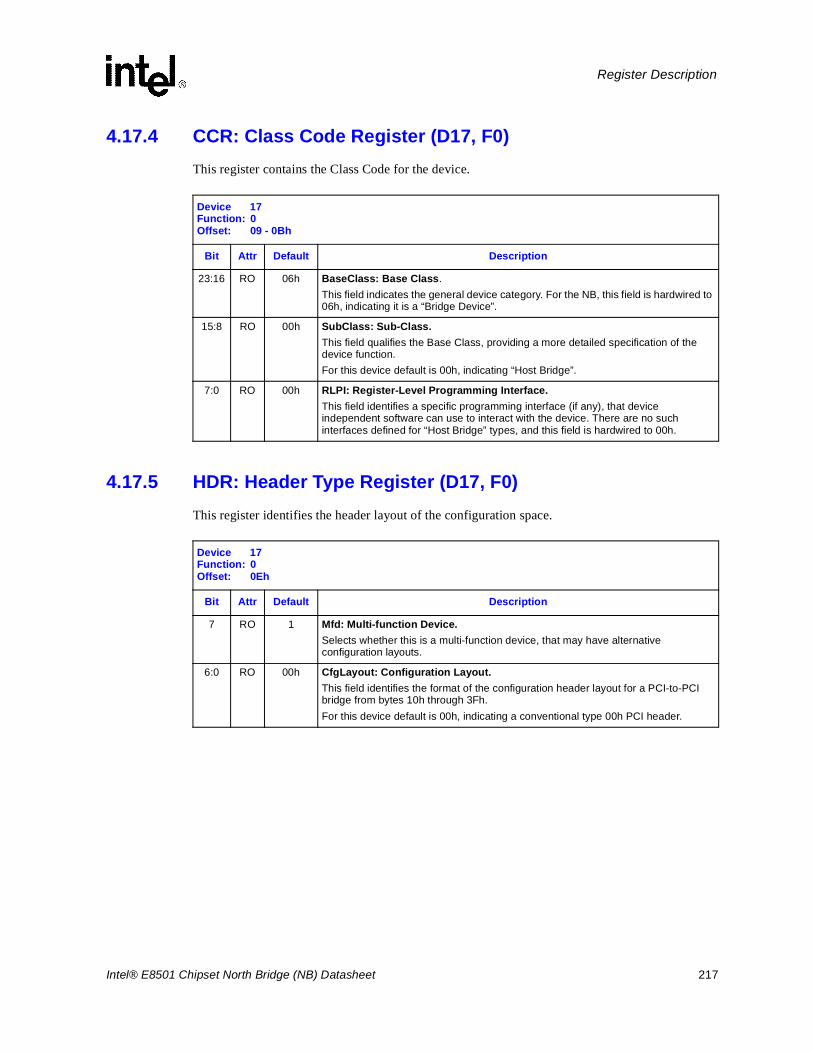
Intel® E8501 Chipset North Bridge (NB) Datasheet 217
Register Description
4.17.4 CCR: Class Code Register (D17, F0)This register contains the Class Code for the device.
4.17.5 HDR: Header Type Register (D17, F0)This register identifies the header layout of the configuration space.
Device 17Function: 0Offset: 09 - 0Bh
Bit Attr Default Description
23:16 RO 06h BaseClass: Base Class.This field indicates the general device category. For the NB, this field is hardwired to 06h, indicating it is a “Bridge Device”.
15:8 RO 00h SubClass: Sub-Class.This field qualifies the Base Class, providing a more detailed specification of the device function. For this device default is 00h, indicating “Host Bridge”.
7:0 RO 00h RLPI: Register-Level Programming Interface.This field identifies a specific programming interface (if any), that device independent software can use to interact with the device. There are no such interfaces defined for “Host Bridge” types, and this field is hardwired to 00h.
Device 17Function: 0Offset: 0Eh
Bit Attr Default Description
7 RO 1 Mfd: Multi-function Device.Selects whether this is a multi-function device, that may have alternative configuration layouts.
6:0 RO 00h CfgLayout: Configuration Layout.This field identifies the format of the configuration header layout for a PCI-to-PCI bridge from bytes 10h through 3Fh. For this device default is 00h, indicating a conventional type 00h PCI header.
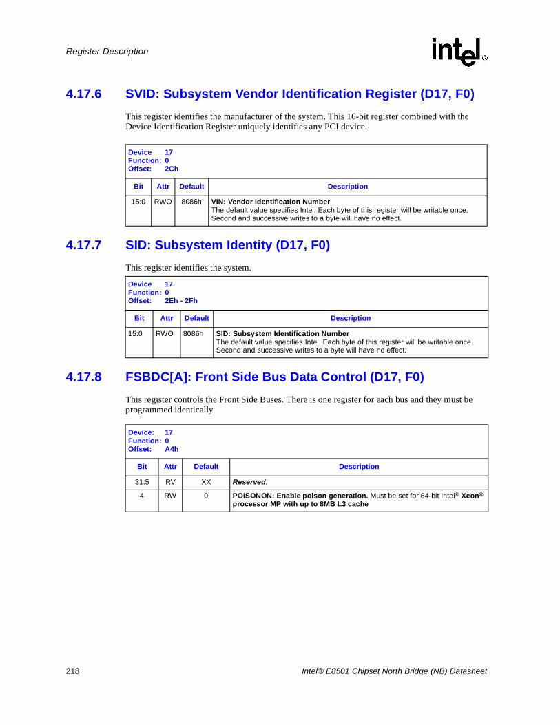
218 Intel® E8501 Chipset North Bridge (NB) Datasheet
Register Description
4.17.6 SVID: Subsystem Vendor Identification Register (D17, F0)This register identifies the manufacturer of the system. This 16-bit register combined with the Device Identification Register uniquely identifies any PCI device.
4.17.7 SID: Subsystem Identity (D17, F0)This register identifies the system.
4.17.8 FSBDC[A]: Front Side Bus Data Control (D17, F0)This register controls the Front Side Buses. There is one register for each bus and they must be programmed identically.
Device 17Function: 0Offset: 2Ch
Bit Attr Default Description
15:0 RWO 8086h VIN: Vendor Identification NumberThe default value specifies Intel. Each byte of this register will be writable once. Second and successive writes to a byte will have no effect.
Device 17Function: 0Offset: 2Eh - 2Fh
Bit Attr Default Description
15:0 RWO 8086h SID: Subsystem Identification Number The default value specifies Intel. Each byte of this register will be writable once. Second and successive writes to a byte will have no effect.
Device: 17Function: 0Offset: A4h
Bit Attr Default Description
31:5 RV XX Reserved.
4 RW 0 POISONON: Enable poison generation. Must be set for 64-bit Intel® Xeon®processor MP with up to 8MB L3 cache
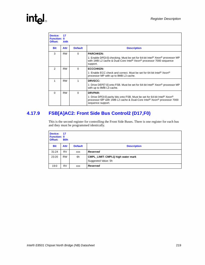
Intel® E8501 Chipset North Bridge (NB) Datasheet 219
Register Description
4.17.9 FSB[A]AC2: Front Side Bus Control2 (D17,F0)This is the second register for controlling the Front Side Buses. There is one register for each bus and they must be programmed identically.
3 RW 0 PARCHKEN: 1: Enable DP[3:0] checking. Must be set for 64-bit Intel® Xeon® processor MP with 1MB L2 cache & Dual-Core Intel® Xeon® processor 7000 sequence support.
2 RW 0 ECCCHKEN: 1: Enable ECC check and correct. Must be set for 64-bit Intel® Xeon®
processor MP with up to 8MB L3 cache.
1 RW 1 DRVECC: 1: Drive DEP[7:0] onto FSB. Must be set for 64-bit Intel® Xeon® processor MP with up to 8MB L3 cache.
0 RW 0 DRVPAR:1: Drive DP[3:0] parity bits onto FSB. Must be set for 64-bit Intel® Xeon®
processor MP with 1MB L2 cache & Dual-Core Intel® Xeon® processor 7000 sequence support.
Device: 17Function: 0Offset: A4h
Bit Attr Default Description
Device: 17Function: 0Offset: B0h
Bit Attr Default Description
31:24 RV xxx Reserved
23:20 RW 6h CMPL_LIMIT: CMPLQ high water markSuggested Value: 5h
19:0 RV xxx Reserved
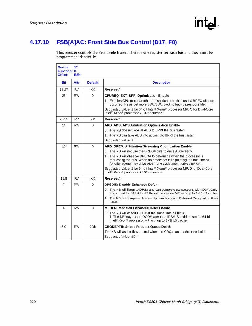
220 Intel® E8501 Chipset North Bridge (NB) Datasheet
Register Description
4.17.10 FSB[A]AC: Front Side Bus Control (D17, F0)This register controls the Front Side Buses. There is one register for each bus and they must be programmed identically.
Device: 17Function: 0Offset: B8h
Bit Attr Default Description
31:27 RV XX Reserved.
26 RW 0 CPUREQ_EXT: BPRI Optimization Enable1: Enables CPU to get another transaction onto the bus if a BREQ change
occurred. Helps get more BWL/BWL back to back cases possible.Suggested Value: 1 for 64-bit Intel® Xeon® processor MP. O for Dual-Core Intel® Xeon® processor 7000 sequence
25:15 RV XX Reserved.
14 RW 0 ARB_ADS: ADS Arbitration Optimization Enable0: The NB doesn’t look at ADS to BPRI the bus faster.1: The NB can take ADS into account to BPRI the bus faster.Suggested Value: 1
13 RW 0 ARB_BREQ: Arbitration Streaming Optimization Enable0: The NB will not use the BREQ# pins to drive ADS# early.1: The NB will observe BREQ# to determine when the processor is
requesting the bus. When no processor is requesting the bus, the NB (priority agent) may drive ADS# one cycle after it drives BPRI#.
Suggested Value: 1 for 64-bit Intel® Xeon® processor MP, 0 for Dual-Core Intel® Xeon® processor 7000 sequence
12:8 RV XX Reserved.
7 RW 0 DPSDIS: Disable Enhanced Defer0: The NB will listen to DPS# and can complete transactions with IDS#. Only
if strapped for 64-bit Intel® Xeon® processor MP with up to 8MB L3 cache 1: The NB will complete deferred transactions with Deferred Reply rather than
IDS#.
6 RW 0 MEDEN: Modified Enhanced Defer Enable0: The NB will assert OOD# at the same time as IDS#.
1: The NB may assert OOD# later than IDS#. Should be set for 64-bit Intel® Xeon® processor MP with up to 8MB L3 cache
5:0 RW 2Dh CRQDEPTH: Snoop Request Queue DepthThe NB will assert flow control when the CRQ reaches this threshold.Suggested Value: 1Dh
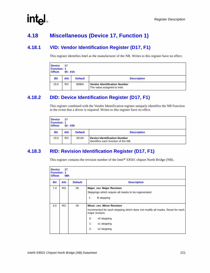
Intel® E8501 Chipset North Bridge (NB) Datasheet 221
Register Description
4.18 Miscellaneous (Device 17, Function 1)
4.18.1 VID: Vendor Identification Register (D17, F1)This register identifies Intel as the manufacturer of the NB. Writes to this register have no effect.
4.18.2 DID: Device Identification Register (D17, F1)This register combined with the Vendor Identification register uniquely identifies the NB Function in the event that a driver is required. Writes to this register have no effect.
4.18.3 RID: Revision Identification Register (D17, F1)This register contains the revision number of the Intel® E8501 chipset North Bridge (NB).
Device 17Function: 1Offset: 00 - 01h
Bit Attr Default Description
15:0 RO 8086h Vendor Identification NumberThe value assigned to Intel.
Device 17Function: 1Offset: 02 - 03h
Bit Attr Default Description
15:0 RO 2614h Device Identification NumberIdentifies each function of the NB.
Device 17Function: 1Offset: 08h
Bit Attr Default Description
7:4 RO 0h Major_rev: Major RevisionSteppings which require all masks to be regenerated.
3:0 RO 0h Minor_rev: Minor RevisionIncremented for each stepping which does not modify all masks. Reset for eachmajor revision.
1: B stepping
0: x0 stepping
1: x1 stepping
2: x2 stepping
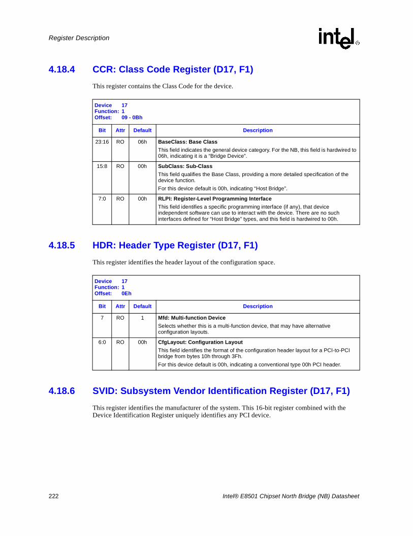
222 Intel® E8501 Chipset North Bridge (NB) Datasheet
Register Description
4.18.4 CCR: Class Code Register (D17, F1)This register contains the Class Code for the device.
4.18.5 HDR: Header Type Register (D17, F1)This register identifies the header layout of the configuration space.
4.18.6 SVID: Subsystem Vendor Identification Register (D17, F1)This register identifies the manufacturer of the system. This 16-bit register combined with the Device Identification Register uniquely identifies any PCI device.
Device 17Function: 1Offset: 09 - 0Bh
Bit Attr Default Description
23:16 RO 06h BaseClass: Base ClassThis field indicates the general device category. For the NB, this field is hardwired to 06h, indicating it is a “Bridge Device”.
15:8 RO 00h SubClass: Sub-ClassThis field qualifies the Base Class, providing a more detailed specification of the device function. For this device default is 00h, indicating “Host Bridge”.
7:0 RO 00h RLPI: Register-Level Programming InterfaceThis field identifies a specific programming interface (if any), that device independent software can use to interact with the device. There are no such interfaces defined for “Host Bridge” types, and this field is hardwired to 00h.
Device 17Function: 1Offset: 0Eh
Bit Attr Default Description
7 RO 1 Mfd: Multi-function DeviceSelects whether this is a multi-function device, that may have alternative configuration layouts.
6:0 RO 00h CfgLayout: Configuration LayoutThis field identifies the format of the configuration header layout for a PCI-to-PCI bridge from bytes 10h through 3Fh. For this device default is 00h, indicating a conventional type 00h PCI header.
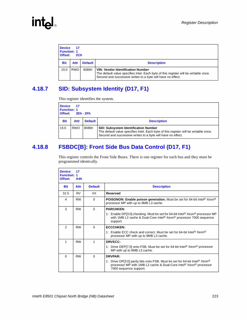
Intel® E8501 Chipset North Bridge (NB) Datasheet 223
Register Description
4.18.7 SID: Subsystem Identity (D17, F1)This register identifies the system.
4.18.8 FSBDC[B]: Front Side Bus Data Control (D17, F1)This register controls the Front Side Buses. There is one register for each bus and they must be programmed identically.
Device 17Function: 1Offset: 2Ch
Bit Attr Default Description
15:0 RWO 8086h VIN: Vendor Identification NumberThe default value specifies Intel. Each byte of this register will be writable once. Second and successive writes to a byte will have no effect.
Device 17Function: 1Offset: 2Eh - 2Fh
Bit Attr Default Description
15:0 RWO 8086h SID: Subsystem Identification Number The default value specifies Intel. Each byte of this register will be writable once. Second and successive writes to a byte will have no effect.
Device: 17Function: 1Offset: A4h
Bit Attr Default Description
31:5 RV XX Reserved.
4 RW 0 POISONON: Enable poison generation. Must be set for 64-bit Intel® Xeon®
processor MP with up to 8MB L3 cache.
3 RW 0 PARCHKEN: 1: Enable DP[3:0] checking. Must be set for 64-bit Intel® Xeon® processor MP
with 1MB L2 cache & Dual-Core Intel® Xeon® processor 7000 sequence support.
2 RW 0 ECCCHKEN: 1: Enable ECC check and correct. Must be set for 64-bit Intel® Xeon®
processor MP with up to 8MB L3 cache.
1 RW 1 DRVECC: 1: Drive DEP[7:0] onto FSB. Must be set for 64-bit Intel® Xeon® processor
MP with up to 8MB L3 cache.
0 RW 0 DRVPAR:1: Drive DP[3:0] parity bits onto FSB. Must be set for 64-bit Intel® Xeon®
processor MP with 1MB L2 cache & Dual-Core Intel® Xeon® processor 7000 sequence support.
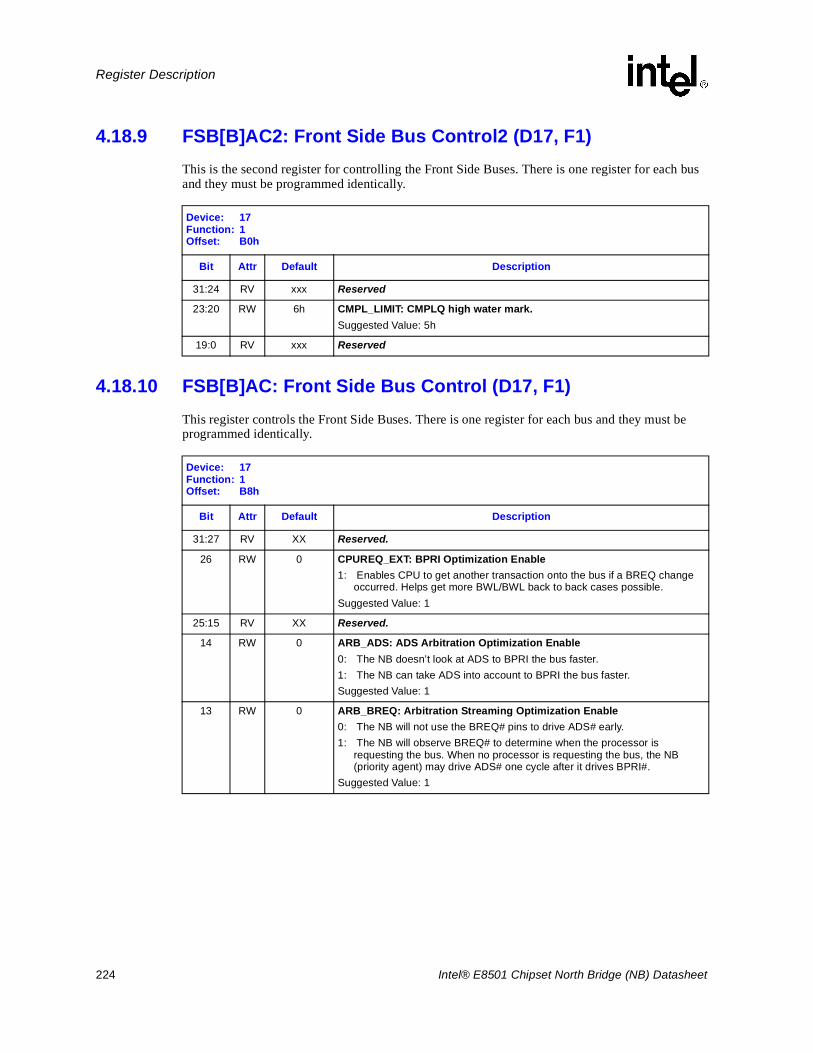
224 Intel® E8501 Chipset North Bridge (NB) Datasheet
Register Description
4.18.9 FSB[B]AC2: Front Side Bus Control2 (D17, F1)This is the second register for controlling the Front Side Buses. There is one register for each bus and they must be programmed identically.
4.18.10 FSB[B]AC: Front Side Bus Control (D17, F1)This register controls the Front Side Buses. There is one register for each bus and they must be programmed identically.
Device: 17Function: 1Offset: B0h
Bit Attr Default Description
31:24 RV xxx Reserved
23:20 RW 6h CMPL_LIMIT: CMPLQ high water mark.Suggested Value: 5h
19:0 RV xxx Reserved
Device: 17Function: 1Offset: B8h
Bit Attr Default Description
31:27 RV XX Reserved.
26 RW 0 CPUREQ_EXT: BPRI Optimization Enable1: Enables CPU to get another transaction onto the bus if a BREQ change
occurred. Helps get more BWL/BWL back to back cases possible.Suggested Value: 1
25:15 RV XX Reserved.
14 RW 0 ARB_ADS: ADS Arbitration Optimization Enable0: The NB doesn’t look at ADS to BPRI the bus faster.1: The NB can take ADS into account to BPRI the bus faster.Suggested Value: 1
13 RW 0 ARB_BREQ: Arbitration Streaming Optimization Enable0: The NB will not use the BREQ# pins to drive ADS# early.1: The NB will observe BREQ# to determine when the processor is
requesting the bus. When no processor is requesting the bus, the NB (priority agent) may drive ADS# one cycle after it drives BPRI#.
Suggested Value: 1
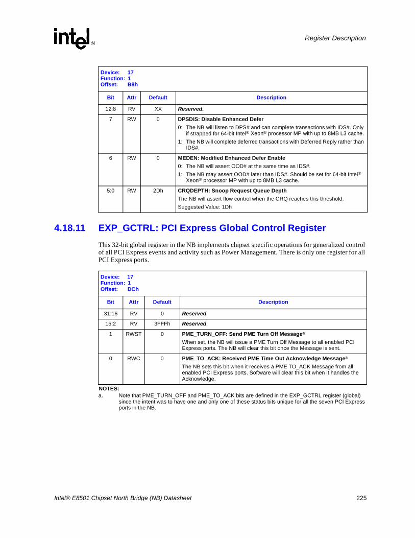
Intel® E8501 Chipset North Bridge (NB) Datasheet 225
Register Description
4.18.11 EXP_GCTRL: PCI Express Global Control RegisterThis 32-bit global register in the NB implements chipset specific operations for generalized control of all PCI Express events and activity such as Power Management. There is only one register for all PCI Express ports.
12:8 RV XX Reserved.
7 RW 0 DPSDIS: Disable Enhanced Defer0: The NB will listen to DPS# and can complete transactions with IDS#. Only
if strapped for 64-bit Intel® Xeon® processor MP with up to 8MB L3 cache.1: The NB will complete deferred transactions with Deferred Reply rather than
IDS#.
6 RW 0 MEDEN: Modified Enhanced Defer Enable0: The NB will assert OOD# at the same time as IDS#.1: The NB may assert OOD# later than IDS#. Should be set for 64-bit Intel®
Xeon® processor MP with up to 8MB L3 cache.
5:0 RW 2Dh CRQDEPTH: Snoop Request Queue DepthThe NB will assert flow control when the CRQ reaches this threshold.Suggested Value: 1Dh
Device: 17Function: 1Offset: B8h
Bit Attr Default Description
Device: 17Function: 1Offset: DCh
Bit Attr Default Description
31:16 RV 0 Reserved.
15:2 RV 3FFFh Reserved.
1 RWST 0 PME_TURN_OFF: Send PME Turn Off Messagea
When set, the NB will issue a PME Turn Off Message to all enabled PCI Express ports. The NB will clear this bit once the Message is sent.
0 RWC 0 PME_TO_ACK: Received PME Time Out Acknowledge Messagea
The NB sets this bit when it receives a PME TO_ACK Message from all enabled PCI Express ports. Software will clear this bit when it handles the Acknowledge.
NOTES:a. Note that PME_TURN_OFF and PME_TO_ACK bits are defined in the EXP_GCTRL register (global)
since the intent was to have one and only one of these status bits unique for all the seven PCI Express ports in the NB.
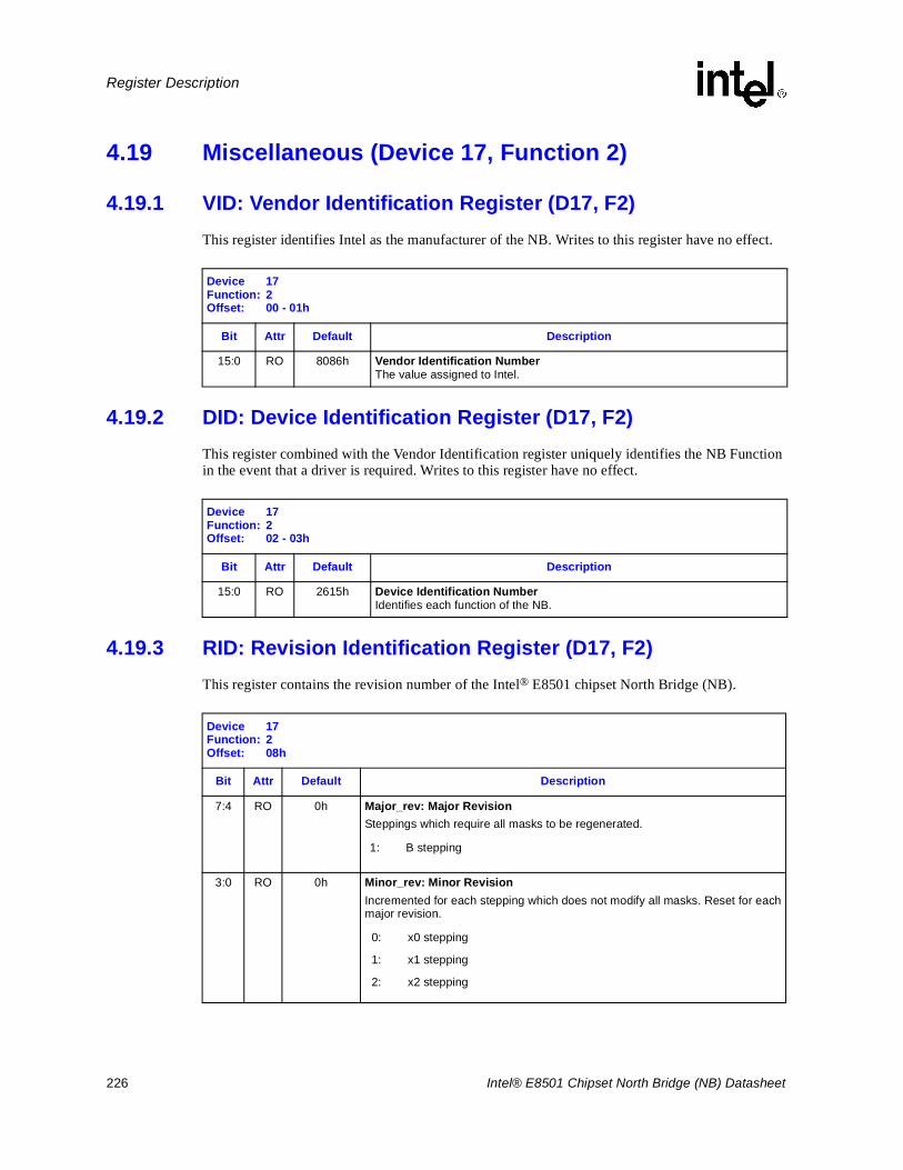
226 Intel® E8501 Chipset North Bridge (NB) Datasheet
Register Description
4.19 Miscellaneous (Device 17, Function 2)
4.19.1 VID: Vendor Identification Register (D17, F2)This register identifies Intel as the manufacturer of the NB. Writes to this register have no effect.
4.19.2 DID: Device Identification Register (D17, F2)This register combined with the Vendor Identification register uniquely identifies the NB Function in the event that a driver is required. Writes to this register have no effect.
4.19.3 RID: Revision Identification Register (D17, F2)This register contains the revision number of the Intel® E8501 chipset North Bridge (NB).
Device 17Function: 2Offset: 00 - 01h
Bit Attr Default Description
15:0 RO 8086h Vendor Identification NumberThe value assigned to Intel.
Device 17Function: 2Offset: 02 - 03h
Bit Attr Default Description
15:0 RO 2615h Device Identification NumberIdentifies each function of the NB.
Device 17Function: 2Offset: 08h
Bit Attr Default Description
7:4 RO 0h Major_rev: Major RevisionSteppings which require all masks to be regenerated.
3:0 RO 0h Minor_rev: Minor RevisionIncremented for each stepping which does not modify all masks. Reset for eachmajor revision.
1: B stepping
0: x0 stepping
1: x1 stepping
2: x2 stepping
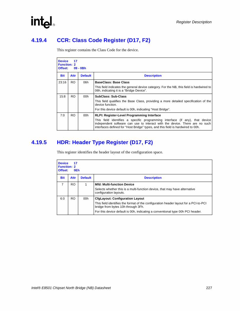
Intel® E8501 Chipset North Bridge (NB) Datasheet 227
Register Description
4.19.4 CCR: Class Code Register (D17, F2)This register contains the Class Code for the device.
4.19.5 HDR: Header Type Register (D17, F2)This register identifies the header layout of the configuration space.
Device 17Function: 2Offset: 09 - 0Bh
Bit Attr Default Description
23:16 RO 06h BaseClass: Base ClassThis field indicates the general device category. For the NB, this field is hardwired to06h, indicating it is a “Bridge Device”.
15:8 RO 00h SubClass: Sub-ClassThis field qualifies the Base Class, providing a more detailed specification of thedevice function. For this device default is 00h, indicating “Host Bridge”.
7:0 RO 00h RLPI: Register-Level Programming InterfaceThis field identifies a specific programming interface (if any), that deviceindependent software can use to interact with the device. There are no suchinterfaces defined for “Host Bridge” types, and this field is hardwired to 00h.
Device 17Function: 2Offset: 0Eh
Bit Attr Default Description
7 RO 1 Mfd: Multi-function DeviceSelects whether this is a multi-function device, that may have alternative configuration layouts.
6:0 RO 00h CfgLayout: Configuration LayoutThis field identifies the format of the configuration header layout for a PCI-to-PCI bridge from bytes 10h through 3Fh. For this device default is 00h, indicating a conventional type 00h PCI header.
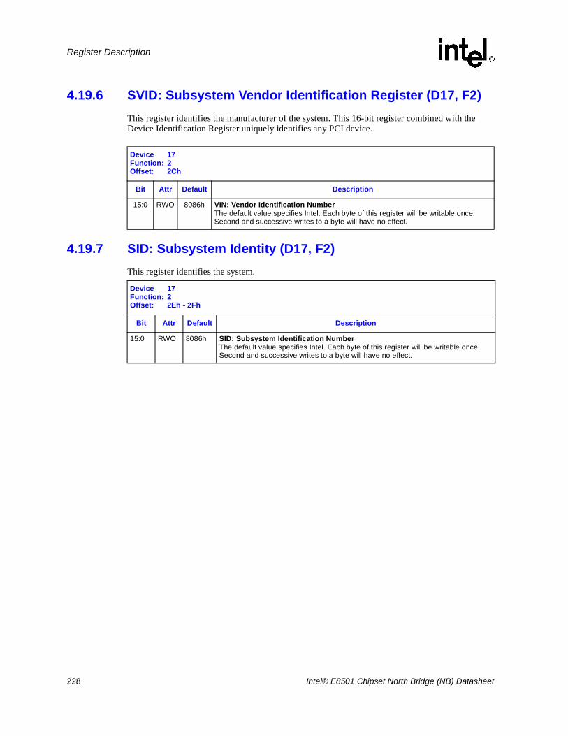
228 Intel® E8501 Chipset North Bridge (NB) Datasheet
Register Description
4.19.6 SVID: Subsystem Vendor Identification Register (D17, F2)This register identifies the manufacturer of the system. This 16-bit register combined with the Device Identification Register uniquely identifies any PCI device.
4.19.7 SID: Subsystem Identity (D17, F2)This register identifies the system.
Device 17Function: 2Offset: 2Ch
Bit Attr Default Description
15:0 RWO 8086h VIN: Vendor Identification NumberThe default value specifies Intel. Each byte of this register will be writable once. Second and successive writes to a byte will have no effect.
Device 17Function: 2Offset: 2Eh - 2Fh
Bit Attr Default Description
15:0 RWO 8086h SID: Subsystem Identification Number The default value specifies Intel. Each byte of this register will be writable once. Second and successive writes to a byte will have no effect.
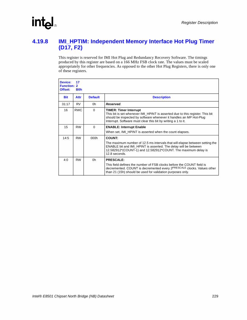
Intel® E8501 Chipset North Bridge (NB) Datasheet 229
Register Description
4.19.8 IMI_HPTIM: Independent Memory Interface Hot Plug Timer(D17, F2)This register is reserved for IMI Hot Plug and Redundancy Recovery Software. The timings produced by this register are based on a 166 MHz FSB clock rate. The values must be scaled appropriately for other frequencies. As opposed to the other Hot Plug Registers, there is only one of these registers.
Device: 17Function: 2Offset: B0h
Bit Attr Default Description
31:17 RV 0h Reserved.
16 RWC 0 TIMER: Timer Interrupt This bit is set whenever IMI_HPINT is asserted due to this register. This bit should be inspected by software whenever it handles an MP Hot-Plug Interrupt. Software must clear this bit by writing a 1 to it.
15 RW 0 ENABLE: Interrupt EnableWhen set, IMI_HPINT is asserted when the count elapses.
14:5 RW 000h COUNT: The maximum number of 12.5 ms intervals that will elapse between setting the ENABLE bit and IMI_HPINT is asserted. The delay will be between 12.582912*(COUNT-1) and 12.582912*COUNT. The maximum delay is 12.8 seconds.
4:0 RW 0h PRESCALE: This field defines the number of FSB clocks before the COUNT field is decremented. COUNT is decremented every 2PRESCALE clocks. Values other than 21 (15h) should be used for validation purposes only.
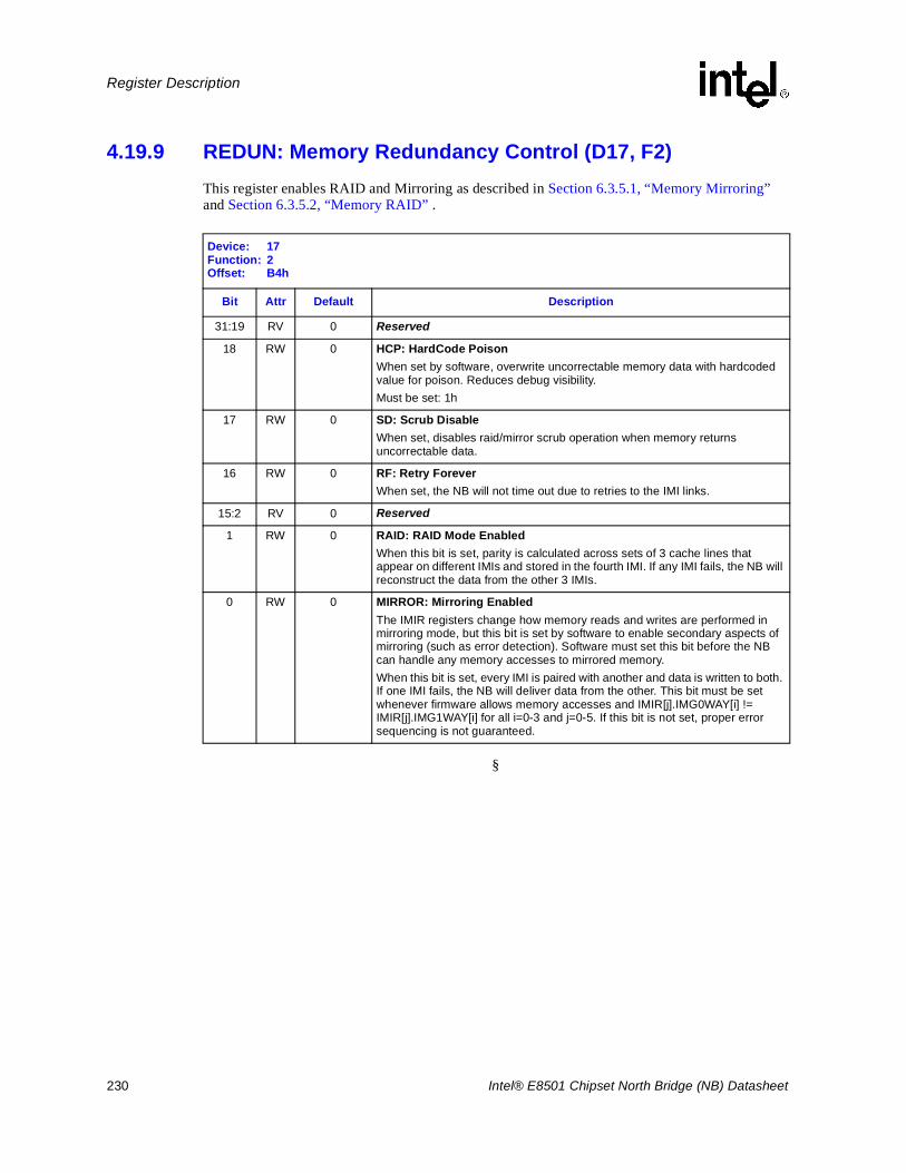
230 Intel® E8501 Chipset North Bridge (NB) Datasheet
Register Description
4.19.9 REDUN: Memory Redundancy Control (D17, F2)This register enables RAID and Mirroring as described in Section 6.3.5.1, “Memory Mirroring” and Section 6.3.5.2, “Memory RAID” .
§
Device: 17Function: 2Offset: B4h
Bit Attr Default Description
31:19 RV 0 Reserved
18 RW 0 HCP: HardCode PoisonWhen set by software, overwrite uncorrectable memory data with hardcoded value for poison. Reduces debug visibility. Must be set: 1h
17 RW 0 SD: Scrub DisableWhen set, disables raid/mirror scrub operation when memory returns uncorrectable data.
16 RW 0 RF: Retry ForeverWhen set, the NB will not time out due to retries to the IMI links.
15:2 RV 0 Reserved
1 RW 0 RAID: RAID Mode EnabledWhen this bit is set, parity is calculated across sets of 3 cache lines that appear on different IMIs and stored in the fourth IMI. If any IMI fails, the NB will reconstruct the data from the other 3 IMIs.
0 RW 0 MIRROR: Mirroring EnabledThe IMIR registers change how memory reads and writes are performed in mirroring mode, but this bit is set by software to enable secondary aspects of mirroring (such as error detection). Software must set this bit before the NB can handle any memory accesses to mirrored memory. When this bit is set, every IMI is paired with another and data is written to both. If one IMI fails, the NB will deliver data from the other. This bit must be set whenever firmware allows memory accesses and IMIR[j].IMG0WAY[i] != IMIR[j].IMG1WAY[i] for all i=0-3 and j=0-5. If this bit is not set, proper error sequencing is not guaranteed.
Intel® E8501 Chipset North Bridge (NB) Datasheet 231
5 System Address Map
This chapter describes the system address maps in memory space, I/O space, and PCI configuration register map.
5.1 Memory MapThe Intel® E8501 chipset platform supports 40 bits of memory address space. All key components and interfaces also support the 40-bit address space.
• The 64-bit Intel® Xeon® processor MP provides address bits for a 40-bit address space.
• 40-bit local address supported over the Independent Memory Interface (IMI) for the memory space.
• 32- and 64-bit address bit formats supported for PCI Express interface.
The chipset treats accesses to various address ranges in different ways. There are fixed ranges like the compatibility region below 1 MB, interrupt delivery range, and the system region located in the 32 MB directly below 4 GB. In addition, there is a variable region for Memory Mapped I/O. The locations of these ranges in the memory map are illustrated in Figure 5-1.
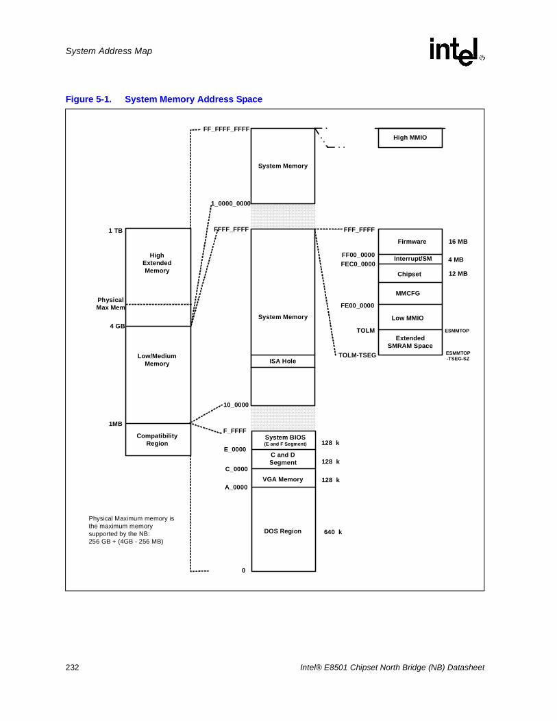
232 Intel® E8501 Chipset North Bridge (NB) Datasheet
System Address Map
Figure 5-1. System Memory Address Space
1 TB
1MB
4 GB
Interrupt/SM
FF_FFFF_FFFF
1_0000_0000
FFFF_FFFF
PhysicalMax Mem
CompatibilityRegion
Low/MediumMemory
HighExtendedMemory
System Memory
System Memory
ISA Hole
System BIOS(E and F Segment)
C and DSegment
VGA Memory
DOS Region
F_FFFF
E_0000
C_0000
A_0000
0
128 k
128 k
128 k
640 k
10_0000
Firmware
Chipset
Low MMIO
MMCFG
ExtendedSMRAM Space
TOLM-TSEG
TOLM
FE00_0000
FF00_0000
FFF_FFFF
4 MB
16 MB
12 MB
High MMIO
FEC0_0000
ESMMTOP-TSEG-SZ
ESMMTOP
Physical Maximum memory isthe maximum memorysupported by the NB:256 GB + (4GB - 256 MB)
Intel® E8501 Chipset North Bridge (NB) Datasheet 233
System Address Map
5.1.1 Compatibility RegionThis is the range from 0-1 MB (0_0000 to F_FFFF). Requests to the Compatibility region are directed to main memory, the Compatibility Bus, or the VGA device. Any physical DRAM that would be addressed by requests in this region that are mapped to the Compatibility Bus is not recovered. This region is divided into four ranges. Regions below 1M that are mapped to memory are accessible by the processors and by any I/O bus.
Note: The DRAM that has a physical address between 0-1 MB must not be recovered or relocated or reflected. This range must always be available to the OS as DRAM, even if at times addresses in this range are sent to the Compatibility Bus, VGA or other non-DRAM areas.
5.1.1.1 Microsoft MS-DOS* Region
Microsoft MS-DOS applications execute in the lowest 640 KB, in the address range 0h to 9_FFFFh. This range is always mapped to main memory.
5.1.1.2 VGA Memory Range
The 128 KB Video Graphics Adapter Memory range (A_0000h to B_FFFFh) can be mapped to the VGA device which may be on any PCI Express or Hub Interface or it can be mapped to main memory (if it is mapped to SMM space). At power-on this space is mapped to the HI port.
Note that the NB chipset does not support the historical MDA (Monochrome Display Adapter) space which would have appeared in the VGA region.
This region can be redirected by BIOS to point to any bus which has a VGA card. If the VGAEN bit is set in one of the NB.BCTRL configuration registers associated with the PCI Express port, then transactions in this space are sent to that PCI Express port. Note that the VGAEN bit can only be set in one and only one of the NB.BCTRL registers. For more information on the BCTRL registers, refer to Section 4.11.27, “BCTRL[7:1]: Bridge Control Register (D1-7, F0)” on page 4-100.
If any VGAEN bits are set, all the ISAEN bits must be set.
This 128 KB region may also be used for mapping SMM space. The SMM range can overlay the VGA range in the A and B segments. If the SMM range overlaps an enabled VGA range then the state of the SMMEM# signal determines where accesses to the SMM Range are directed. SMMEM# asserted directs the accesses to the memory and SMMEM# deasserted directs the access to the PCI Express bus where VGA has been mapped.
This region cannot be cached.
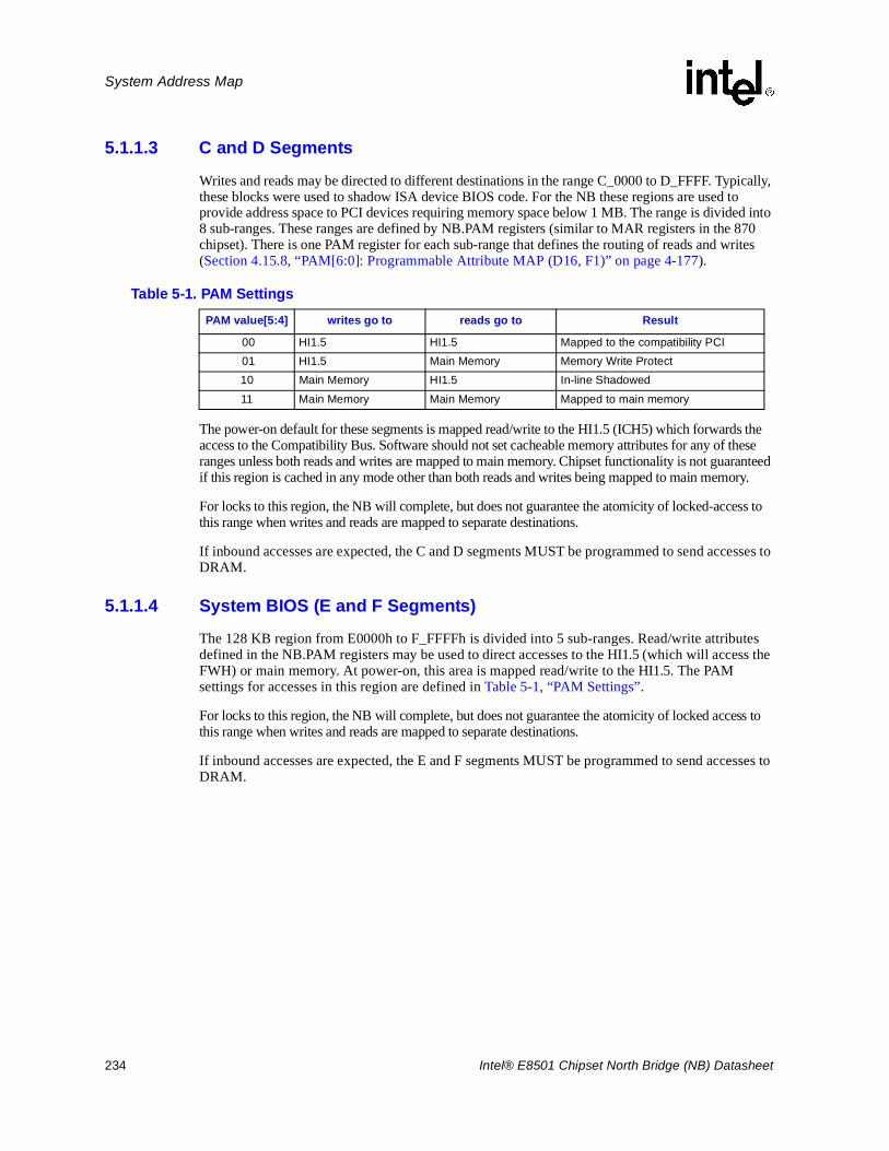
234 Intel® E8501 Chipset North Bridge (NB) Datasheet
System Address Map
5.1.1.3 C and D Segments
Writes and reads may be directed to different destinations in the range C_0000 to D_FFFF. Typically, these blocks were used to shadow ISA device BIOS code. For the NB these regions are used to provide address space to PCI devices requiring memory space below 1 MB. The range is divided into 8 sub-ranges. These ranges are defined by NB.PAM registers (similar to MAR registers in the 870 chipset). There is one PAM register for each sub-range that defines the routing of reads and writes (Section 4.15.8, “PAM[6:0]: Programmable Attribute MAP (D16, F1)” on page 4-177).
The power-on default for these segments is mapped read/write to the HI1.5 (ICH5) which forwards the access to the Compatibility Bus. Software should not set cacheable memory attributes for any of these ranges unless both reads and writes are mapped to main memory. Chipset functionality is not guaranteed if this region is cached in any mode other than both reads and writes being mapped to main memory.
For locks to this region, the NB will complete, but does not guarantee the atomicity of locked-access to this range when writes and reads are mapped to separate destinations.
If inbound accesses are expected, the C and D segments MUST be programmed to send accesses to DRAM.
5.1.1.4 System BIOS (E and F Segments)
The 128 KB region from E0000h to F_FFFFh is divided into 5 sub-ranges. Read/write attributes defined in the NB.PAM registers may be used to direct accesses to the HI1.5 (which will access the FWH) or main memory. At power-on, this area is mapped read/write to the HI1.5. The PAM settings for accesses in this region are defined in Table 5-1, “PAM Settings”.
For locks to this region, the NB will complete, but does not guarantee the atomicity of locked access to this range when writes and reads are mapped to separate destinations.
If inbound accesses are expected, the E and F segments MUST be programmed to send accesses to DRAM.
Table 5-1. PAM SettingsPAM value[5:4] writes go to reads go to Result
00 HI1.5 HI1.5 Mapped to the compatibility PCI 01 HI1.5 Main Memory Memory Write Protect10 Main Memory HI1.5 In-line Shadowed
11 Main Memory Main Memory Mapped to main memory
Intel® E8501 Chipset North Bridge (NB) Datasheet 235
System Address Map
5.1.2 Low/Medium MemoryThe low/medium memory regions range from 1 MB to 4 GB. It consists of sub-regions for Firmware, Processor memory mapped functions, and NB chipset specific registers.
5.1.2.1 System Memory
See Section 5.1.4, “Main Memory Region” .
5.1.2.2 ISA Hole
An ISA “window” can be optionally opened up between 15 MB and 16 MB by setting the NB.FDHC.HEN bit. If this bit is set, accesses to this region will be sent to the ICH5 via the HI1.5. Otherwise, it is decoded as a system memory access. The memory behind this hole cannot be reclaimed.
5.1.2.3 Extended SMRAM Space (TSEG)
SMM space allows system management software to partition a region in main memory that is only accessible by system management software. When the SMM range is enabled, memory in this range is not exposed to the Operating System. The SMM range is accessed only when the processor is in SMM-mode. This is an extended SMM range that is different than the SMM space that may reside that overlaps VGA space. The register fields that define the NB.EXSMRC.TSEG_SZ and NB.EXSMRTOP.ESMMTOP. The TSEG SMM space starts at ESMMTOP-TSEG_SZ and ends at ESMMTOP. This region may be 128KB, 256KB, or 1MB in size, depending on the TSEG_SZ field. ESMMTOP is relocatable to accommodate software that wishes to configure the TSEG SMM space before MMIO space is known. The ESMMTOP will default to the same value as TOLM.
If SMM is enabled, the chipset allows accesses to this range only when the SMMEM# signal on the FSB is asserted with the request.
If SMMEM# is deasserted, accesses to the SMM Range are master aborted. If SMMEM# is asserted the access is routed to main memory. The NB will use the SMM enable and range registers to determine where to route the access.
The NB will not support a locked-access that crosses an SMM boundary. Firmware should not create data structures that span this boundary.
SMM main memory is protected from Inbound accesses.
Note: In order to make cacheable SMM possible, the chipset must accept EWB’s (BWL’s) and must absorb IWB (HITM) data regardless of the condition of the SMMEM# pin. Because of this, care must be used when attempting to cache SMM space. The chipset/platform cannot protect against processor which attempts to illegally access SMM space that is modified in another processor’s cache. Any software that creates such a condition (for example, by corrupting the page table) will jeopardize the protective properties of SMM.
See Table 5-9 “Decoding Processor Requests to SMM and VGA Spaces” on page 5-257 for details on SMM decoding.
236 Intel® E8501 Chipset North Bridge (NB) Datasheet
System Address Map
5.1.2.4 Memory Mapped Configuration Region
There is one relocatable memory mapped configuration regions on the NB. The FSB address defines the configuration register to be accessed and the FSB data either returns or provides register contents. As opposed to CF8/CFC-based configuration accesses, this mechanism is atomic. The memory mapped configuration region is compatible with the PCI Express enhanced configuration mechanism. It is a 256MB window that maps to PCI Express registers. (Both in the chipset and south of the chipset.) The location of this MMCFG window is defined by the NB.EXP_ECBASE register (Section 4.15.13).
The default value of NB.EXP_ECBASE maps these regions into a region where there will be no wasted memory that is lost behind it. The default value for the PCI Express registers is 0100_0000. If this range is moved, the following recommendations will enable reclaiming the memory that is lost to MMCFG accesses.
1. MMCFG range is mapped to a legal location within the range between TOLM and 4GB. Since ranges must not overlap other legal ranges, it is safest to put this range between TOLM and the lowest real MMIO range (The current default is in these ranges).
OR
2. Put the regions above 4GB (above the top of memory and not overlapping above 4GB MMIO space).
This space is also accessible inbound. To protect the chipset under normal operation, inbound accesses can be protected by the NB.EXP_CTRL.DIS_INB_CFG bit (Section 4.11.28).
BIOS/software must ensure there are no outstanding configuration accesses or memory accesses to the old and new MMCFG range addresses when relocating this range.
5.1.2.5 Low Memory Mapped I/O (MMIO)
This is the first of the two NB memory mapped I/O ranges. The low memory mapped I/O range is defined to be between TOLM and FE00_0000h. This low MMIO region is further subdivided between the PCI Express and HI1.5 (ICH5) ports. The following table shows the registers used to define the MMIO ranges for each PCI Express/HI device. These registers are compatible with PCI Express and the PCI-to-PCI bridge specifications. Note that all subranges must be contained in the low memory mapped I/O range (between TOLM and FE00_0000h). In other words, the lowest base address must be above TOLM and the highest LIMIT register must be below FE00_0000h. Subranges must also not overlap each other.
Table 5-2. Low Memory Mapped I/Oa (Sheet 1 of 2)
I/O Port NB Base NB Limit
HI (ICH5) N/Ab
PCI Express D Memory MBASE1 (MBASE in device 1) MLIMIT1 (MLIMIT in device 1)
PCI Express D Prefetchable Memory PMBASE1 (MBASE in device 1) PMLIMIT1 (MLIMIT in device 1)
PCI Express C0 Memory MBASE2 MLIMIT2
PCI Express C0 Prefetchable Memory PMBASE2 PMLIMIT2
PCI Express C1 Memory MBASE3 MLIMIT3
Intel® E8501 Chipset North Bridge (NB) Datasheet 237
System Address Map
The NB will decode addresses in this range and route them to the appropriate HI1.5 or PCI Express port. If the address is in the low MMIO range, but is not contained in any of the PCI Express base and limit ranges, it will be routed to the HI1.5.
If the NB.PMLU and NB.PMBU registers are greater than 0, than the corresponding prefetchable region will be located in the high MMIO range instead.
5.1.2.6 Chipset Specific Range
The address range FE00_0000h - FEBF_FFFFh region is reserved for chipset specific functions.
• FE60_C000h - FE6F_FFFFh: This range is used for memory mapped NB registers. They are accessible only from the FSB. These registers are fixed since they are needed early during the boot process. The registers include:
a. 4 Scratch Pad Registers
b. 4 Sticky Scratch Pad Registers
c. 4 Boot flag registers
d. 4 Repeatability registersThese registers are described in the NB Configuration Register Chapter.
Only the first 4 bytes of each 1 K block in this 16 K range is accepted by the NB. The NB will issue requests to the remainder of this region to the ICH unless they map into one of the relocatable regions such as MMCFG. The mechanism for this range can be the same as it is for the memory mapped configuration accesses.
5.1.2.7 Interrupt/LT Region
This 4 MB range is used for processor specific applications. It lies between FEC0_0000h and FEEF_FFFFh and is split into four 1 MB segments.
PCI Express C1 Prefetchable Memory PMBASE3 PMLIMIT3
PCI Express B0 Memory MBASE4 MLIMIT4
PCI Express B0 Prefetchable Memory PMBASE4 PMLIMIT4
PCI Express B1 Memory MBASE5 MLIMIT5
PCI Express B1 Prefetchable Memory PMBASE5 PMLIMIT5
PCI Express A0 Memory MBASE6 MLIMIT6
PCI Express A0 Prefetchable Memory PMBASE6 PMLIMIT6
PCI Express A1 Memory MBASE7 MLIMIT7
PCI Express A1 Prefetchable Memory PMBASE7 PMLIMIT7NOTES:a. This table assumes NB.PMLU and NB.PMBU are 0’s. Otherwise, the prefetchable memory space will be located in high
MMIO space.b. NB does not need base/limit for ICH5 because subtractive decoding will send the accesses to the ICH5. This is OK for
software also, since the ICH5 is considered part of the same bus as the NB.
Table 5-2. Low Memory Mapped I/Oa (Sheet 2 of 2)
I/O Port NB Base NB Limit
238 Intel® E8501 Chipset North Bridge (NB) Datasheet
System Address Map
5.1.2.7.1 I/O APIC Controller Range
This address range FEC0_0000 to FEC8_FFFF is used to communicate with the IOAPIC controllers in the Intel 6700PXH/6702PXH 64-bit PCI Hub, or ICH5.
The APIC ranges are hard coded. Reads and writes to each IOAPIC region should be sent to the appropriate HI1.5 or PCI Express as indicated below.
For hot-plug IOAPIC support, it is recommended that software use the standard MMIO range to communicate to the Intel 6700PXH 64-bit PCI Hub. To accomplish this, the PXH.MBAR must be programmed within the PCI Express device MMIO region.
Inbound accesses to this memory range should also be routed to the I/O APIC controllers. This could happen if software configures MSI devices to send MSI’s to an I/O APIC controller.
Figure 5-2. Interrupt Region
I/O APIC
High SMM
Reserved
Interrupt
Route to ICH5
Route to ICH5
Route to ICH5 (MMT =FED0_0000-FED0_3FFF)
FEC8_FFFF
FEC0_0000
FEC9_0000
FED2_0000
FED3_FFFF
FEDA_0000
FEDA_FFFF
FEE0_0000
FEEF_FFFF
Table 5-3. IOAPIC Address MappingIOAPIC0 (HI1.5) 0_FEC0_0000 to 0_FEC7_FFFFa
NOTES:a. IOAPIC range is hard coded on the ICH5
IOAPIC1 (PCI Express D) 0_FEC8_0000 to 0_FEC8_0FFF
IOAPIC2 (PCI Express C0) 0_FEC8_1000 to 0_FEC8_1FFF
IOAPIC3 (PCI Express C1) 0_FEC8_2000 to 0_FEC8_2FFF
IOAPIC4 (PCI Express B0) 0_FEC8_3000 to 0_FEC8_3FFF
IOAPIC5 (PCI Express B1) 0_FEC8_4000 to 0_FEC8_4FFF
IOAPIC6 (PCI Express A0) 0_FEC8_5000 to 0_FEC8_5FFF
IOAPIC7 (PCI Express A1) 0_FEC8_6000 to 0_FEC8_6FFF
Reserved 0_FEC8_7000 to 0_FEC8_FFFF
Intel® E8501 Chipset North Bridge (NB) Datasheet 239
System Address Map
5.1.2.7.2 High SMM Range
If high SMM space is enabled by EXSMRC.H_SMRAME, then requests to the address range from FEDA_0000 to FEDB_FFFF will be aliased down to the physical address of A_0000 to B_FFFF. The HIGHSMM space allows cacheable accesses to the compatible (legacy) SMM space. In this range, the chipset will accept EWB’s (BWL’s) regardless of the SMMEM# pin. Also, if there is an implicit writeback (HITM with data), the chipset will update memory with the new data (regardless of the SMMEM# pin). Note that if the HIGHSMM space is enabled, the aliased SMM space of A_0000-B_FFFF will be disabled.
Note: In order to make cacheable SMM possible, the chipset must accept EWB’s (BWL’s) and must absorb IWB (HITM) data regardless of the condition of the SMMEM# pin. Because of this, care must be used when attempting to cache SMM space. The chipset/platform cannot protect against processors who attempt to illegally access SMM space that is modified in another processor’s cache. Any software that creates such a condition (for example, by corrupting the page table) will jeopardize the protective properties of SMM.
5.1.2.7.3 Interrupt Range
Requests to the address range FEE0_0000 to FEEF_FFFF are used to deliver interrupts. Memory reads or write transactions to this range are illegal from the processor. The processor issues interrupt transactions to this range. Inbound interrupts from the PCI Express devices in the form of memory writes to this range are converted by the NB to FSB interrupt requests.
5.1.2.7.4 Reserved Ranges
The NB will master abort requests to the remaining addresses in the interrupt range. This is the FEF0_0000h - FEFF_FFFFh or FED4_0000h - FEDF_FFFFh ranges. This can be done by sending the request to the compatibility bus (Hub Interface) to be master aborted. In the event the ICH5 adds new registers or functionality in this range in the future, this provides the most likely chance that it will work.
5.1.2.8 Firmware Range
The Intel® E8501 chipset platform allocates 16MB of firmware space from FF00_0000h to FFFF_FFFFh. Requests in this range are directed to the Compatibility Bus. The ICH5 will route these to its FWH interface. This range is accessible from any FSB.
5.1.3 High Extended MemoryThis is the range above 4 GB. The range from 4 GB to NB.IMIR5.LIMIT is mapped to system memory. There can also be a memory mapped I/O region is located at the top of the address space. (Just below 1TB). This is described in Section 5.1.3.2.
5.1.3.1 System Memory
See Section 5.1.4, “Main Memory Region” .
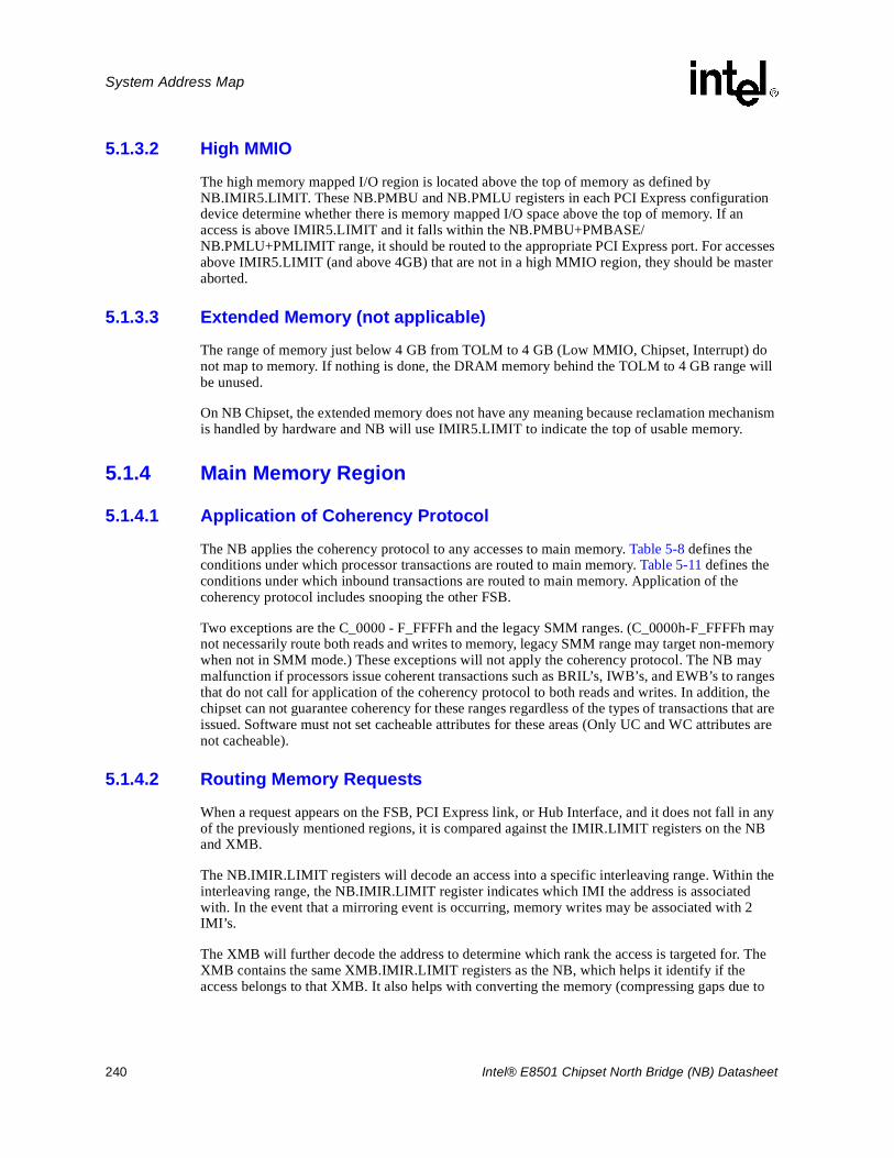
240 Intel® E8501 Chipset North Bridge (NB) Datasheet
System Address Map
5.1.3.2 High MMIO
The high memory mapped I/O region is located above the top of memory as defined by NB.IMIR5.LIMIT. These NB.PMBU and NB.PMLU registers in each PCI Express configuration device determine whether there is memory mapped I/O space above the top of memory. If an access is above IMIR5.LIMIT and it falls within the NB.PMBU+PMBASE/ NB.PMLU+PMLIMIT range, it should be routed to the appropriate PCI Express port. For accesses above IMIR5.LIMIT (and above 4GB) that are not in a high MMIO region, they should be master aborted.
5.1.3.3 Extended Memory (not applicable)
The range of memory just below 4 GB from TOLM to 4 GB (Low MMIO, Chipset, Interrupt) do not map to memory. If nothing is done, the DRAM memory behind the TOLM to 4 GB range will be unused.
On NB Chipset, the extended memory does not have any meaning because reclamation mechanism is handled by hardware and NB will use IMIR5.LIMIT to indicate the top of usable memory.
5.1.4 Main Memory Region
5.1.4.1 Application of Coherency Protocol
The NB applies the coherency protocol to any accesses to main memory. Table 5-8 defines the conditions under which processor transactions are routed to main memory. Table 5-11 defines the conditions under which inbound transactions are routed to main memory. Application of the coherency protocol includes snooping the other FSB.
Two exceptions are the C_0000 - F_FFFFh and the legacy SMM ranges. (C_0000h-F_FFFFh may not necessarily route both reads and writes to memory, legacy SMM range may target non-memory when not in SMM mode.) These exceptions will not apply the coherency protocol. The NB may malfunction if processors issue coherent transactions such as BRIL’s, IWB’s, and EWB’s to ranges that do not call for application of the coherency protocol to both reads and writes. In addition, the chipset can not guarantee coherency for these ranges regardless of the types of transactions that are issued. Software must not set cacheable attributes for these areas (Only UC and WC attributes are not cacheable).
5.1.4.2 Routing Memory Requests
When a request appears on the FSB, PCI Express link, or Hub Interface, and it does not fall in any of the previously mentioned regions, it is compared against the IMIR.LIMIT registers on the NB and XMB.
The NB.IMIR.LIMIT registers will decode an access into a specific interleaving range. Within the interleaving range, the NB.IMIR.LIMIT register indicates which IMI the address is associated with. In the event that a mirroring event is occurring, memory writes may be associated with 2 IMI’s.
The XMB will further decode the address to determine which rank the access is targeted for. The XMB contains the same XMB.IMIR.LIMIT registers as the NB, which helps it identify if the access belongs to that XMB. It also helps with converting the memory (compressing gaps due to
Intel® E8501 Chipset North Bridge (NB) Datasheet 241
System Address Map
MMIO or IMI interleaving policies). The XMB.DMIR.LIMIT registers also decode the access into a specific interleaving range, which helps decode which rank the access will be directed to. The XMB will also convert the address into the appropriate DDR address, RAS, and CAS signals.
5.1.5 Main Memory interleavingMemory interleaving can be described at two levels. The lowest level of memory interleaving is at the XMB level where DIMMs/Ranks are interleaved. The highest level of memory interleaving is between IMI ports. Interleaving can be at a fine or coarse granularity. Fine granularity interleaves at the cacheline boundary and provides optimal performance by evenly distributing memory accesses when addresses are accessed somewhat linearly. It helps eliminate hot spots. Coarse granularity interleaves on a boundary that is much coarser than a cacheline, for example, a different address range for each IMI (which some may call 1:1 interleaving). Coarse interleaving enables certain RAS features. A combination of fine and course interleaving will probably achieve the optimal mix of performance and RAS.
The NB supports 6 interleave ranges to interleave across the IMI’s. Each range supports 4 way (4:1), 2 way (2:1), or 1 way (1:1) interleaving. The NB.IMIR registers contain the address of the top of the interleave range, the primary and secondary IMI ports (for mirroring) for each way.
The XMB tracks the same 6 interleave ranges. In addition, the XMB supports 5 interleave ranges to interleave across the 8 DIMM ranks. The XMB also comprehends gaps in the address to do MMIO space and IMI interleaving. The MMIO gap is accounted for using the TOLM register and is described in detail in Section 5.1.5.4, “Recovering Main Memory Behind Other Regions” . The other gaps due to IMI interleaving are handled by setting the interleave range associated with that address range to not point to any ranks on the XMB.
The interleaving scheme also comprehends mirroring across IMI’s, RAID, and DIMM pair sparing. For mirroring, each way of each NB.IMIR register contains a primary and secondary port. Writes are sent to both ports. Reads are sent to one port depending. For RAID, interleaving must use 4 interleaving ranges to enable RAID striping. For sparing (on the XMB), the XMB.DIMIRs reflect the live DIMM ranks. If a sparing event occurs, the DMIR will be automatically updated with the spare DIMM rank.
5.1.5.1 Interleaving Registers
The NB and XMB contain the following registers to support the ranges to do IMI and DIMM rank interleaving.
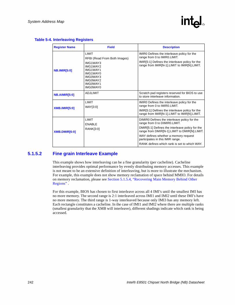
242 Intel® E8501 Chipset North Bridge (NB) Datasheet
System Address Map
5.1.5.2 Fine grain Interleave Example
This example shows how interleaving can be a fine granularity (per cacheline). Cacheline interleaving provides optimal performance by evenly distributing memory accesses. This example is not meant to be an extensive definition of interleaving, but is more to illustrate the mechanism. For example, this example does not show memory reclamation of space behind MMIO. For details on memory reclamation, please see Section 5.1.5.4, “Recovering Main Memory Behind Other Regions” .
For this example, BIOS has chosen to first interleave across all 4 IMI’s until the smallest IMI has no more memory. The second range is 2:1 interleaved across IMI1 and IMI2 until these IMI’s have no more memory. The third range is 1-way interleaved because only IMI3 has any memory left. Each rectangle constitutes a cacheline. In the case of IMI1 and IMI2 where there are multiple ranks (smallest granularity that the XMB will interleave), different shadings indicate which rank is being accessed.
Table 5-4. Interleaving Registers
Register Name Field Description
NB.IMIR[5:0]
LIMITRFBI (Read From Both Images)IMG1WAY3IMG1WAY2IMG1WAY1IMG1WAY0IMG0WAY3IMG0WAY2IMG0WAY1IMG0WAY0
IMIR0 Defines the interleave policy for the range from 0 to IMIR0.LIMIT.IMIR[5:1] Defines the interleave policy for the range from IMIR[N-1].LIMIT to IMIR[N].LIMIT.
NB.AIMIR[5:0] ADJLIMIT Scratch pad registers reserved for BIOS to use to store interleave information.
XMB.IMIR[5:0]
LIMITWAY[3:0]
IMIR0 Defines the interleave policy for the range from 0 to IMIR0.LIMIT.IMIR[5:1] Defines the interleave policy for the range from IMIR[N-1].LIMIT to IMIR[N].LIMIT.
XMB.DMIR[6:0]
LIMITENABLERANK[3:0]
DIMIR0 Defines the interleave policy for the range from 0 to DIMIR0.LIMIT.DMIR[5:1] Defines the interleave policy for the range from DMIR[N-1].LIMIT to DMIR[N].LIMIT.WAY defines whether a memory request participates in this IMIR range.RANK defines which rank is set to which WAY.
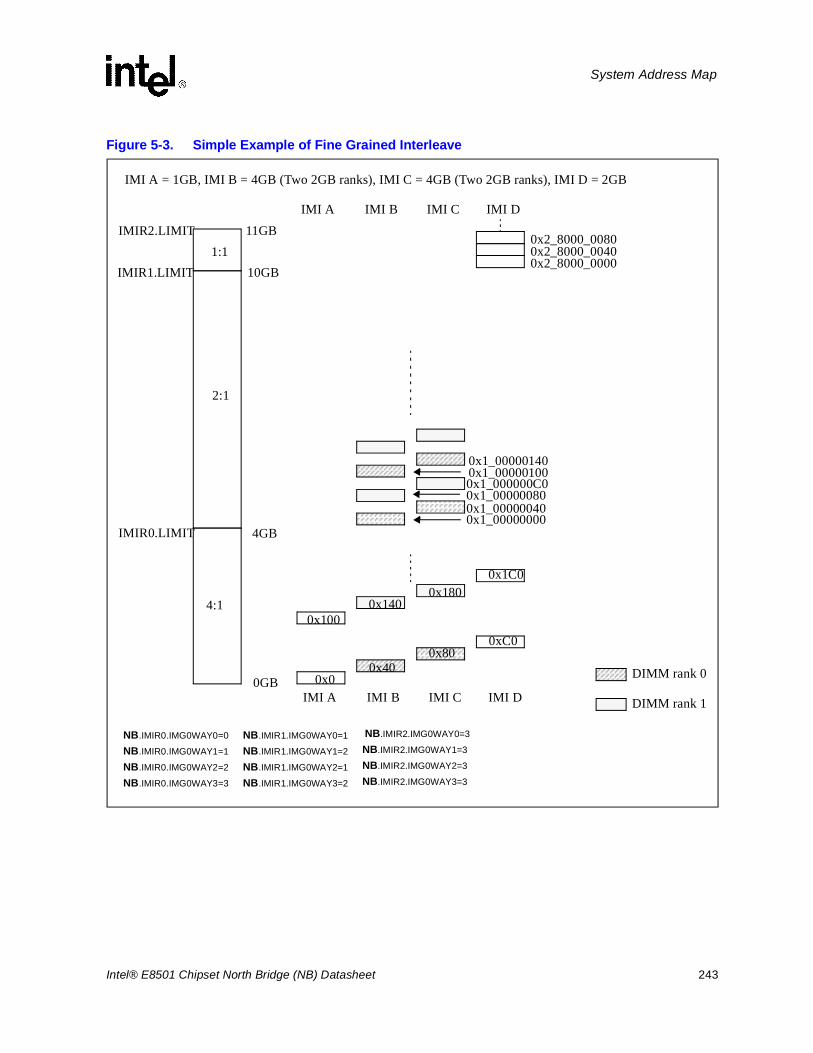
Intel® E8501 Chipset North Bridge (NB) Datasheet 243
System Address Map
Figure 5-3. Simple Example of Fine Grained Interleave
IMI A = 1GB, IMI B = 4GB (Two 2GB ranks), IMI C = 4GB (Two 2GB ranks), IMI D = 2GB
4GB
4:1
10GB
2:1
11GB1:1
0GBIMI A IMI B IMI DIMI C
0x00x40
0x800xC0
0x100
0x1_000000000x1_000000400x1_000000800x1_000000C0
IMIR0.LIMIT
IMIR1.LIMIT
IMIR2.LIMITIMI A IMI B IMI DIMI C
0x2_8000_00400x2_8000_0080
0x2_8000_0000
0x1400x180
DIMM rank 0
DIMM rank 1
0x1_000001000x1_00000140
0x1C0
NB.IMIR0.IMG0WAY0=0
NB.IMIR0.IMG0WAY1=1
NB.IMIR0.IMG0WAY2=2
NB.IMIR0.IMG0WAY3=3
NB.IMIR1.IMG0WAY0=1
NB.IMIR1.IMG0WAY1=2
NB.IMIR1.IMG0WAY2=1
NB.IMIR1.IMG0WAY3=2
NB.IMIR2.IMG0WAY0=3
NB.IMIR2.IMG0WAY1=3
NB.IMIR2.IMG0WAY2=3
NB.IMIR2.IMG0WAY3=3
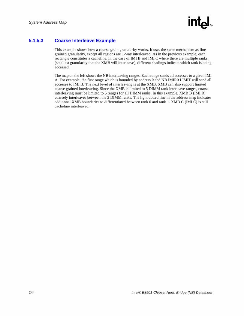
244 Intel® E8501 Chipset North Bridge (NB) Datasheet
System Address Map
5.1.5.3 Coarse Interleave Example
This example shows how a course grain granularity works. It uses the same mechanism as fine grained granularity, except all regions are 1-way interleaved. As in the previous example, each rectangle constitutes a cacheline. In the case of IMI B and IMI C where there are multiple ranks (smallest granularity that the XMB will interleave), different shadings indicate which rank is being accessed.
The map on the left shows the NB interleaving ranges. Each range sends all accesses to a given IMI A. For example, the first range which is bounded by address 0 and NB.IMIR0.LIMIT will send all accesses to IMI B. The next level of interleaving is at the XMB. XMB can also support limited coarse grained interleaving. Since the XMB is limited to 5 DIMM rank interleave ranges, coarse interleaving must be limited to 5 ranges for all DIMM ranks. In this example, XMB B (IMI B) coarsely interleaves between the 2 DIMM ranks. The light dotted line in the address map indicates additional XMB boundaries to differentiated between rank 0 and rank 1. XMB C (IMI C) is still cacheline interleaved.
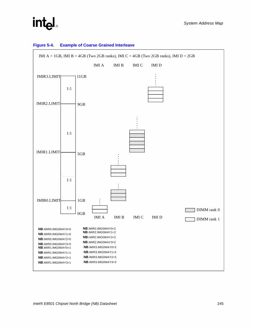
Intel® E8501 Chipset North Bridge (NB) Datasheet 245
System Address Map
Figure 5-4. Example of Coarse Grained Interleave
IMI A = 1GB, IMI B = 4GB (Two 2GB ranks), IMI C = 4GB (Two 2GB ranks), IMI D = 2GB
1GB
1:1
11GB
1:1
1:1
0GBIMI A IMI B IMI DIMI C
IMIR0.LIMIT
IMIR1.LIMIT
IMIR2.LIMIT
IMI A IMI B IMI DIMI C
DIMM rank 0
DIMM rank 1
1:1
5GB
9GB
IMIR3.LIMIT
NB.IMIR0.IMG0WAY0=0
NB.IMIR0.IMG0WAY1=0
NB.IMIR0.IMG0WAY2=0
NB.IMIR0.IMG0WAY3=0NB.IMIR1.IMG0WAY0=1
NB.IMIR1.IMG0WAY1=1
NB.IMIR1.IMG0WAY2=1
NB.IMIR1.IMG0WAY3=1
NB.IMIR2.IMG0WAY0=2NB.IMIR2.IMG0WAY1=2
NBI.MIR2.IMG0WAY2=2
NB.IMIR2.IMG0WAY3=2
NB.IMIR3.IMG0WAY0=3
NB.IMIR3.IMG0WAY1=3
NB.IMIR3.IMG0WAY2=3
NB.IMIR3.IMG0WAY3=3
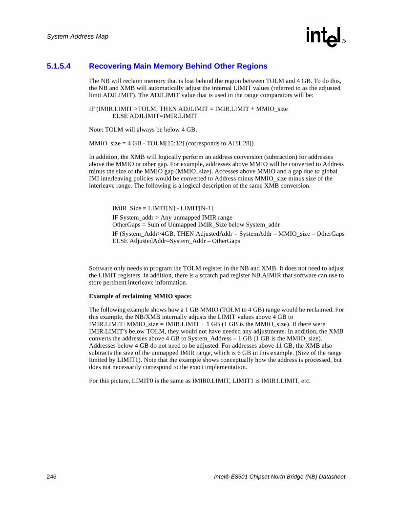
246 Intel® E8501 Chipset North Bridge (NB) Datasheet
System Address Map
5.1.5.4 Recovering Main Memory Behind Other Regions
The NB will reclaim memory that is lost behind the region between TOLM and 4 GB. To do this, the NB and XMB will automatically adjust the internal LIMIT values (referred to as the adjusted limit ADJLIMIT). The ADJLIMIT value that is used in the range comparators will be:
IF (IMIR.LIMIT >TOLM, THEN ADJLIMIT = IMIR.LIMIT + MMIO_sizeELSE ADJLIMIT=IMIR.LIMIT
Note: TOLM will always be below 4 GB.
MMIO_size = 4 GB - TOLM[15:12] (corresponds to A[31:28])
In addition, the XMB will logically perform an address conversion (subtraction) for addresses above the MMIO or other gap. For example, addresses above MMIO will be converted to Address minus the size of the MMIO gap (MMIO_size). Accesses above MMIO and a gap due to global IMI interleaving policies would be converted to Address minus MMIO_size minus size of the interleave range. The following is a logical description of the same XMB conversion.
IMIR_Size = LIMIT[N] - LIMIT[N-1]IF System_addr > Any unmapped IMIR rangeOtherGaps = Sum of Unmapped IMIR_Size below System_addrIF (System_Addr>4GB, THEN AdjustedAddr = SystemAddr – MMIO_size – OtherGapsELSE AdjustedAddr=System_Addr – OtherGaps
Software only needs to program the TOLM register in the NB and XMB. It does not need to adjust the LIMIT registers. In addition, there is a scratch pad register NB.AIMIR that software can use to store pertinent interleave information.
Example of reclaiming MMIO space:
The following example shows how a 1 GB MMIO (TOLM to 4 GB) range would be reclaimed. For this example, the NB/XMB internally adjusts the LIMIT values above 4 GB to IMIR.LIMIT+MMIO_size = IMIR.LIMIT + 1 GB (1 GB is the MMIO_size). If there were IMIR.LIMIT’s below TOLM, they would not have needed any adjustments. In addition, the XMB converts the addresses above 4 GB to System_Address – 1 GB (1 GB is the MMIO_size). Addresses below 4 GB do not need to be adjusted. For addresses above 11 GB, the XMB also subtracts the size of the unmapped IMIR range, which is 6 GB in this example. (Size of the range limited by LIMIT1). Note that the example shows conceptually how the address is processed, but does not necessarily correspond to the exact implementation.
For this picture, LIMIT0 is the same as IMIR0.LIMIT, LIMIT1 is IMIR1.LIMIT, etc.
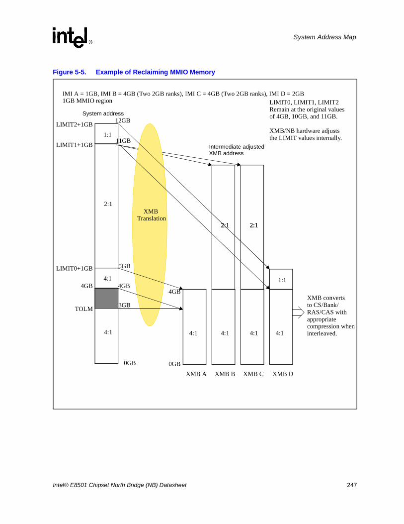
Intel® E8501 Chipset North Bridge (NB) Datasheet 247
System Address Map
Figure 5-5. Example of Reclaiming MMIO Memory
XMB Translation
IMI A = 1GB, IMI B = 4GB (Two 2GB ranks), IMI C = 4GB (Two 2GB ranks), IMI D = 2GB
4GB
4:1
11GB
2:1
12GB
1:1
0GB
LIMIT0+1GB
LIMIT1+1GB
LIMIT2+1GB
4:1
3GB
1GB MMIO region
5GB
Intermediate adjusted
System address
4GB
4:1
2:1
1:1
0GB
LIMIT0, LIMIT1, LIMIT2Remain at the original valuesof 4GB, 10GB, and 11GB.
XMB/NB hardware adjuststhe LIMIT values internally.
XMB address
4:1
2:1
4:14:1
2:12:1
XMB B XMB CXMB A XMB D
XMB convertsto CS/Bank/RAS/CAS withappropriatecompression when interleaved.
4GB
TOLM
248 Intel® E8501 Chipset North Bridge (NB) Datasheet
System Address Map
5.1.5.5 Interleaving
A number of memory RAS features involve removing or adding memory to the system. Care must be exercised in the interleaving definition to balance RAS robustness with optimal interleaving for performance. For example, the interleaving shouldn’t be set up so that removing a DIMM rank results in removing all system memory.
5.1.5.5.1 Interleaving with sparing
If DIMM sparing (without graceful degradation) is desired, at configuration time, a DIMM rank must be set aside to replace a defective DIMM rank. This spare DIMM must not be included in the IMIR and DMIR settings.
5.1.5.5.2 The Effects of Graceful Degradation & Sparing on Interleaving
Graceful degradation is when the memory associated with a bad DIMM rank is removed by software deallocating the memory. If memory is in a region that is pinned (i.e. cannot be removed), an unrelated DIMM pair can be chosen to be deallocated. Once it is deallocated, it can be converted into a spare DIMM.
This feature relies on restrictions to hardware configurations and interleaving policies to be robust. For example, If the DIMMs are interleaved so that none are a good candidate for being a spare, then a spare cannot be made. Software can follow the suggestions below to increase the chance that there will be a good candidate for a spare.
Interleaving restrictions (SW):
1. For each XMB, select a rank that can become a spare.This rank must be the largest of all populated ranks.
a. If there are any split DIMM’s, then the spare must be a split DIMM.
b. Since all DIMM’s will meet minimum DIMM size restriction, any DIMM can be selected to be predestined to be a spare.
2. Interleave the remaining DIMMs. The amount of memory allowable below 4 GB depends on the size of the spare rank. The memory below 4 GB must be able to fit into the spare. For example, if the spare DIMM pair holds 1 GB, then the remaining DIMM’s must only have 1 GB of memory below 4 GB.
Put the spare rank above 4 GB. It must be non-interleaved (i.e. 1:1). Restrictions on hardware include:
1. If there are any double sided DIMM’s, then there needs to be at least 2 double-sided DIMMs.
2. Minimum memory capacity must be larger than 4 GB.
3. Each XMB must have at least 2 DIMM pairs.
4. Restrict the use of small DIMM’s. The DIMM size restrictions are dependent the number of XMB’s and the IMI interleaving. The following table shows the smallest DIMM size allowable for different configurations. These restrictions are to guarantee that even with limited interleaving to allow for this functionality, there will be full memory.
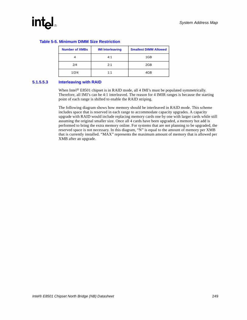
Intel® E8501 Chipset North Bridge (NB) Datasheet 249
System Address Map
5.1.5.5.3 Interleaving with RAID
When Intel® E8501 chipset is in RAID mode, all 4 IMI’s must be populated symmetrically. Therefore, all IMI’s can be 4:1 interleaved. The reason for 4 IMIR ranges is because the starting point of each range is shifted to enable the RAID striping.
The following diagram shows how memory should be interleaved in RAID mode. This scheme includes space that is reserved in each range to accommodate capacity upgrades. A capacity upgrade with RAID would include replacing memory cards one by one with larger cards while still assuming the original smaller size. Once all 4 cards have been upgraded, a memory hot add is performed to bring the extra memory online. For systems that are not planning to be upgraded, the reserved space is not necessary. In this diagram, “N” is equal to the amount of memory per XMB that is currently installed. “MAX” represents the maximum amount of memory that is allowed per XMB after an upgrade.
Table 5-5. Minimum DIMM Size Restriction
Number of XMBs IMI Interleaving Smallest DIMM Allowed
4 4:1 1GB
2/4 2:1 2GB
1/2/4 1:1 4GB
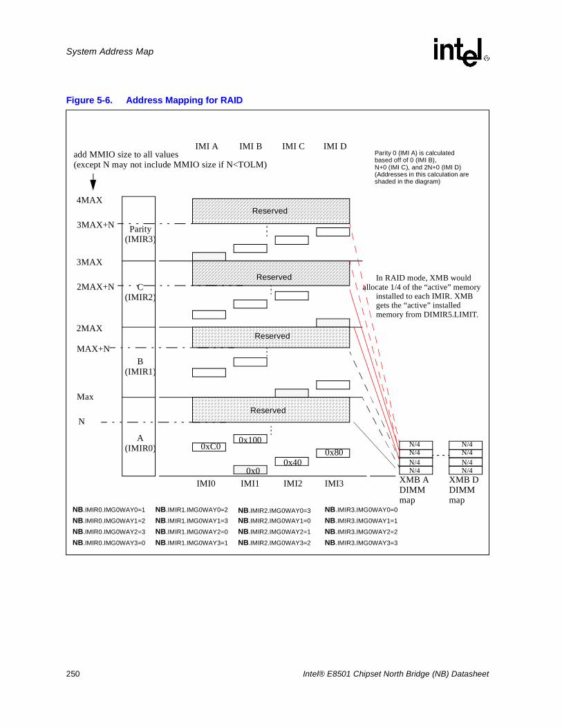
250 Intel® E8501 Chipset North Bridge (NB) Datasheet
System Address Map
Figure 5-6. Address Mapping for RAID
A
IMI0 IMI1 IMI3IMI20x0
0x400x80
0xC0
Max
IMI A IMI B IMI DIMI C
NB.IMIR0.IMG0WAY0=1
NB.IMIR0.IMG0WAY1=2
NB.IMIR0.IMG0WAY2=3
NB.IMIR0.IMG0WAY3=0
NB.IMIR1.IMG0WAY0=2
NB.IMIR1.IMG0WAY1=3
NB.IMIR1.IMG0WAY2=0
NB.IMIR1.IMG0WAY3=1
NB.IMIR2.IMG0WAY0=3NB.IMIR2.IMG0WAY1=0
NB.IMIR2.IMG0WAY2=1
NB.IMIR2.IMG0WAY3=2
B
Parity
(IMIR0)
(IMIR1)
C(IMIR2)
(IMIR3)
NB.IMIR3.IMG0WAY0=0
NB.IMIR3.IMG0WAY1=1
NB.IMIR3.IMG0WAY2=2
NB.IMIR3.IMG0WAY3=3
Parity 0 (IMI A) is calculatedbased off of 0 (IMI B), N+0 (IMI C), and 2N+0 (IMI D)
2MAX
3MAX
4MAX
N
MAX+N
2MAX+N
3MAX+N
add MMIO size to all values
In RAID mode, XMB would
gets the “active” installed memory from DIMIR5.LIMIT.
allocate 1/4 of the “active” memory installed to each IMIR. XMB
XMB ADIMM
XMB DDIMM
N/4N/4
N/4N/4
N/4N/4
N/4N/4
map map
(Addresses in this calculation areshaded in the diagram)
Reserved
Reserved
Reserved
Reserved
0x100
(except N may not include MMIO size if N<TOLM)
Intel® E8501 Chipset North Bridge (NB) Datasheet 251
System Address Map
5.1.5.5.4 Interleaving with Mirroring
Only the NB is aware of mirroring. The NB.IMIR registers have WAY fields defined for both image 0 and image 1 (IMG{1/0}WAY[3:0]). The memory on both IMI’s that are being mirrored should be the same size, so the IMI interleaving algorithm will result in the same settings for both IMI’s. The only difference is that one of the IMI’s is image 0 and the other is image 1. For example, if IMI A and IMI B are mirrored images and IMI C and IMI D are mirrored images, software could cacheline interleave between IMI A/B and IMI C/D by setting the IMIR register as follows:
IMIR.IMG0WAY0 = IMI AIMIR.IMG1WAY0 = IMI BIMIR.IMG0WAY1 = IMI CIMIR.IMG1WAY1 = IMI DIMIR.IMG0WAY2 = IMI AIMIR.IMG1WAY2 = IMI BIMIR.IMG0WAY3 = IMI CIMIR.IMG1WAY3 = IMI D
5.1.6 General Interleaving Guidelines1. There can be no enabled XMB.DMIRs above a disabled DMIR. For example, if DMIR[3] is
disabled, DMIR[5:4] must be disabled.
2. All memory mapped I/O above 4GB (PMBASE/PMLIMIT/PMLU/PMBU) must be higher than the highest IMIR.LIMIT value plus the MMIO hole.
3. For IMIR.LIMIT values above 4GB, the value in IMIR.LIMIT cannot exceed IMIR.LIMIT minus the size of the MMIO hole, since the NB will internally adjust the LIMIT value to IMIR.LIMIT+MMIO hole.
4. Unused NB.IMIR registers should have their IMIR.LIMIT programmed to the same as the LIMIT of the highest functional IMIR. Similarly, unused XMB.DMIR and XMB.IMIR registers should have their LIMIT set to the same as the highest function IMIR/DMIR.
5. For optimal performance when doing 2-way interleaving only on the XMB, the XMB DMIR ways (called RANK[3:0]) should be programmed so that consecutive ways do not go to the same rank.For example, if you have two ranks “m” and “n”, the four ways should be programmed as follows:
Similarly, if a NB is doing 2:1 interleaving (2 IMI’s in the IMIR range), the ways (NB.IMIR.IMG*WAY*) should be programmed so consecutive ways do not go to the same rank.
Way 0 Way 1 Way 2 Way 3 OR Way 0 Way 1 Way 2 Way 3
n m n m m n m n
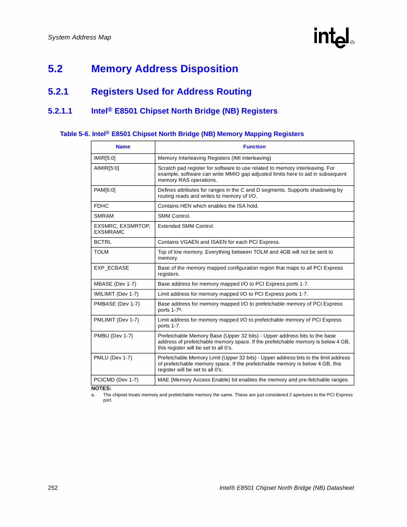
252 Intel® E8501 Chipset North Bridge (NB) Datasheet
System Address Map
5.2 Memory Address Disposition
5.2.1 Registers Used for Address Routing
5.2.1.1 Intel® E8501 Chipset North Bridge (NB) Registers
Table 5-6. Intel® E8501 Chipset North Bridge (NB) Memory Mapping Registers
Name Function
IMIR[5:0] Memory Interleaving Registers (IMI interleaving)
AIMIR[5:0] Scratch pad register for software to use related to memory interleaving. For example, software can write MMIO gap adjusted limits here to aid in subsequent memory RAS operations.
PAM[6:0] Defines attributes for ranges in the C and D segments. Supports shadowing by routing reads and writes to memory of I/O.
FDHC Contains HEN which enables the ISA hold.
SMRAM SMM Control.
EXSMRC, EXSMRTOP, EXSMRAMC
Extended SMM Control.
BCTRL Contains VGAEN and ISAEN for each PCI Express.
TOLM Top of low memory. Everything between TOLM and 4GB will not be sent to memory.
EXP_ECBASE Base of the memory mapped configuration region that maps to all PCI Express registers.
MBASE (Dev 1-7) Base address for memory mapped I/O to PCI Express ports 1-7.
IMILIMIT (Dev 1-7) Limit address for memory mapped I/O to PCI Express ports 1-7.
PMBASE (Dev 1-7) Base address for memory mapped I/O to prefetchable memory of PCI Express ports 1-7a.
NOTES:a. The chipset treats memory and prefetchable memory the same. These are just considered 2 apertures to the PCI Express
port.
PMLIMIT (Dev 1-7) Limit address for memory mapped I/O to prefetchable memory of PCI Express ports 1-7.
PMBU (Dev 1-7) Prefetchable Memory Base (Upper 32 bits) - Upper address bits to the base address of prefetchable memory space. If the prefetchable memory is below 4 GB, this register will be set to all 0’s.
PMLU (Dev 1-7) Prefetchable Memory Limit (Upper 32 bits) - Upper address bits to the limit address of prefetchable memory space. If the prefetchable memory is below 4 GB, this register will be set to all 0’s.
PCICMD (Dev 1-7) MAE (Memory Access Enable) bit enables the memory and pre-fetchable ranges.
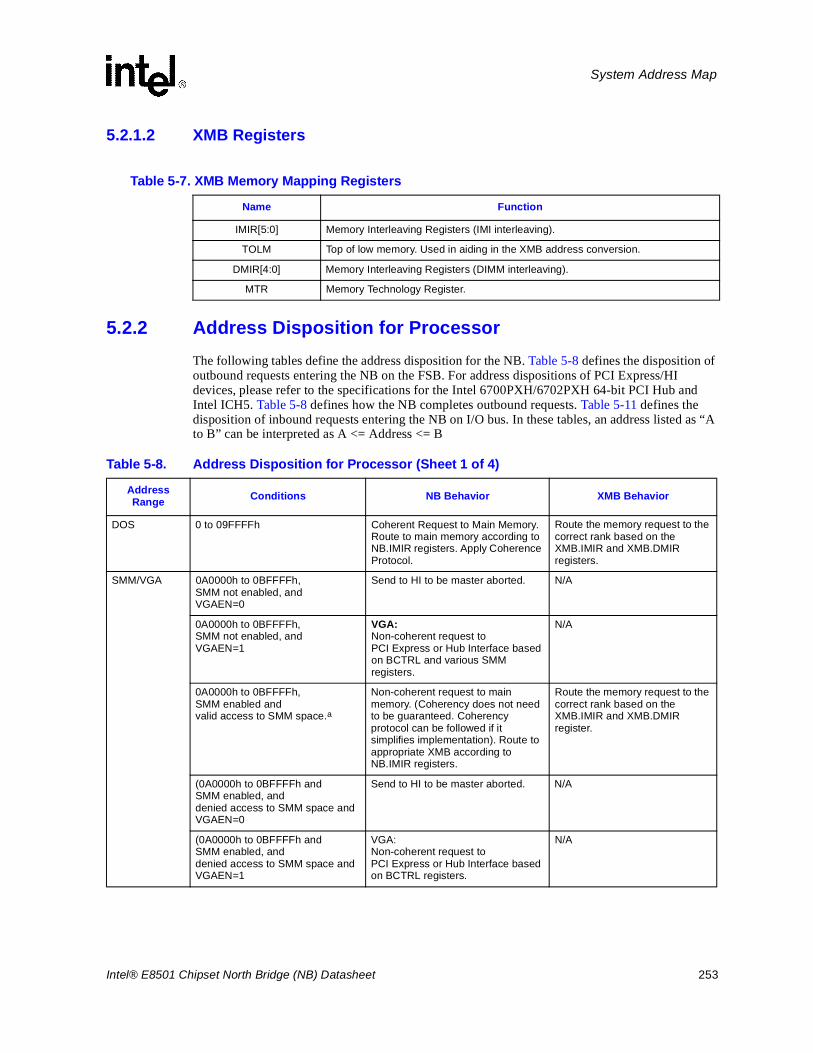
Intel® E8501 Chipset North Bridge (NB) Datasheet 253
System Address Map
5.2.1.2 XMB Registers
5.2.2 Address Disposition for ProcessorThe following tables define the address disposition for the NB. Table 5-8 defines the disposition of outbound requests entering the NB on the FSB. For address dispositions of PCI Express/HI devices, please refer to the specifications for the Intel 6700PXH/6702PXH 64-bit PCI Hub and Intel ICH5. Table 5-8 defines how the NB completes outbound requests. Table 5-11 defines the disposition of inbound requests entering the NB on I/O bus. In these tables, an address listed as “A to B” can be interpreted as A <= Address <= B
Table 5-7. XMB Memory Mapping Registers
Name Function
IMIR[5:0] Memory Interleaving Registers (IMI interleaving).
TOLM Top of low memory. Used in aiding in the XMB address conversion.
DMIR[4:0] Memory Interleaving Registers (DIMM interleaving).
MTR Memory Technology Register.
Table 5-8. Address Disposition for Processor (Sheet 1 of 4)
Address Range Conditions NB Behavior XMB Behavior
DOS 0 to 09FFFFh Coherent Request to Main Memory. Route to main memory according to NB.IMIR registers. Apply Coherence Protocol.
Route the memory request to the correct rank based on the XMB.IMIR and XMB.DMIR registers.
SMM/VGA 0A0000h to 0BFFFFh, SMM not enabled, and VGAEN=0
Send to HI to be master aborted. N/A
0A0000h to 0BFFFFh, SMM not enabled, and VGAEN=1
VGA:Non-coherent request to PCI Express or Hub Interface based on BCTRL and various SMM registers.
N/A
0A0000h to 0BFFFFh,SMM enabled andvalid access to SMM space.a
Non-coherent request to main memory. (Coherency does not need to be guaranteed. Coherency protocol can be followed if it simplifies implementation). Route to appropriate XMB according to NB.IMIR registers.
Route the memory request to the correct rank based on the XMB.IMIR and XMB.DMIR register.
(0A0000h to 0BFFFFh and SMM enabled, anddenied access to SMM space and VGAEN=0
Send to HI to be master aborted. N/A
(0A0000h to 0BFFFFh and SMM enabled, anddenied access to SMM space and VGAEN=1
VGA: Non-coherent request to PCI Express or Hub Interface based on BCTRL registers.
N/A
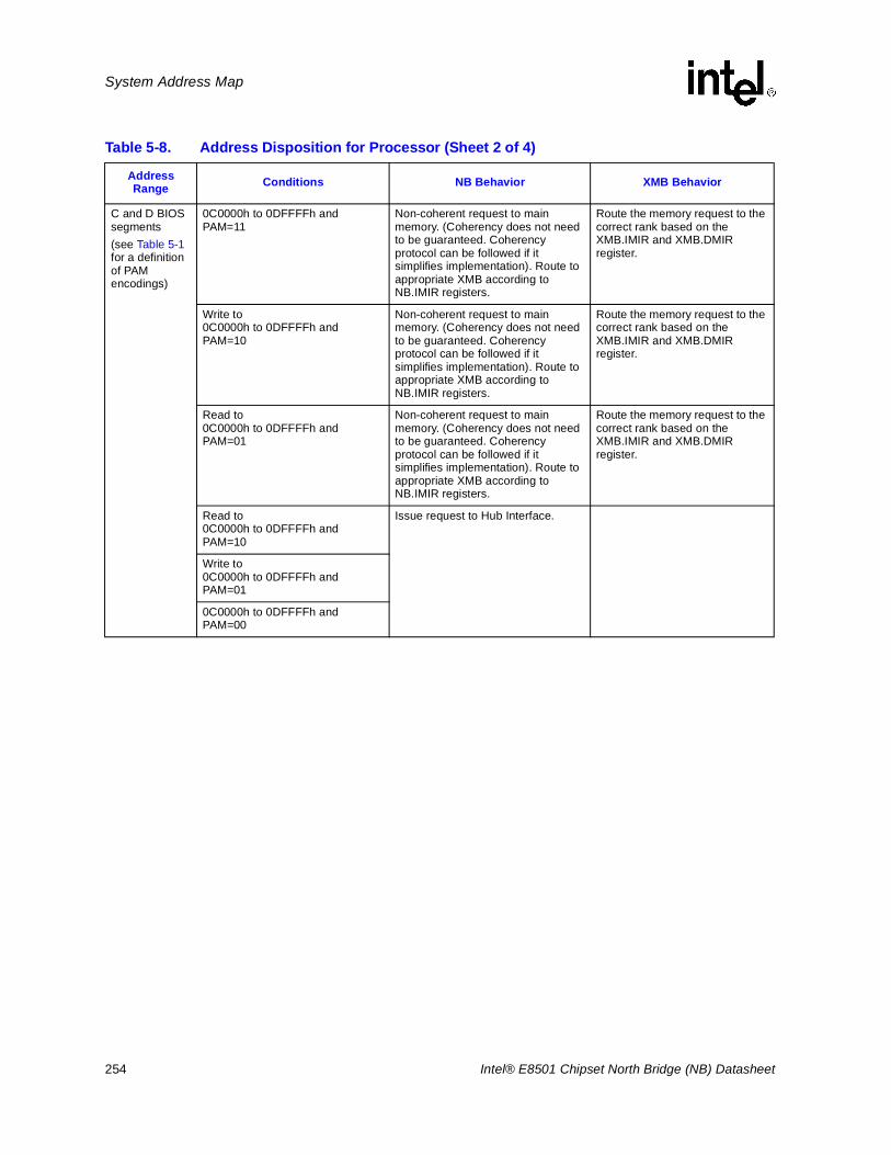
254 Intel® E8501 Chipset North Bridge (NB) Datasheet
System Address Map
C and D BIOS segments(see Table 5-1for a definition of PAM encodings)
0C0000h to 0DFFFFh and PAM=11
Non-coherent request to main memory. (Coherency does not need to be guaranteed. Coherency protocol can be followed if it simplifies implementation). Route to appropriate XMB according to NB.IMIR registers.
Route the memory request to the correct rank based on the XMB.IMIR and XMB.DMIR register.
Write to 0C0000h to 0DFFFFh and PAM=10
Non-coherent request to main memory. (Coherency does not need to be guaranteed. Coherency protocol can be followed if it simplifies implementation). Route to appropriate XMB according to NB.IMIR registers.
Route the memory request to the correct rank based on the XMB.IMIR and XMB.DMIR register.
Read to 0C0000h to 0DFFFFh and PAM=01
Non-coherent request to main memory. (Coherency does not need to be guaranteed. Coherency protocol can be followed if it simplifies implementation). Route to appropriate XMB according to NB.IMIR registers.
Route the memory request to the correct rank based on the XMB.IMIR and XMB.DMIR register.
Read to 0C0000h to 0DFFFFh and PAM=10
Issue request to Hub Interface.
Write to 0C0000h to 0DFFFFh and PAM=01
0C0000h to 0DFFFFh and PAM=00
Table 5-8. Address Disposition for Processor (Sheet 2 of 4)
Address Range Conditions NB Behavior XMB Behavior
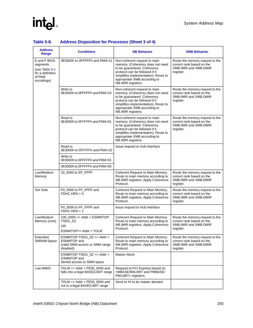
Intel® E8501 Chipset North Bridge (NB) Datasheet 255
System Address Map
E and F BIOS segments(see Table 5-1for a definition of PAM encodings)
0E0000h to 0FFFFFh and PAM=11 Non-coherent request to main memory. (Coherency does not need to be guaranteed. Coherency protocol can be followed if it simplifies implementation). Route to appropriate XMB according to NB.IMIR registers.
Route the memory request to the correct rank based on the XMB.IMIR and XMB.DMIR register.
Write to 0E0000h to 0FFFFFh and PAM=10
Non-coherent request to main memory. (Coherency does not need to be guaranteed. Coherency protocol can be followed if it simplifies implementation). Route to appropriate XMB according to NB.IMIR registers.
Route the memory request to the correct rank based on the XMB.IMIR and XMB.DMIR register.
Read to 0E0000h to 0FFFFFh and PAM=01
Non-coherent request to main memory. (Coherency does not need to be guaranteed. Coherency protocol can be followed if it simplifies implementation). Route to appropriate XMB according to NB.IMIR registers.
Route the memory request to the correct rank based on the XMB.IMIR and XMB.DMIR register.
Read to 0E0000h to 0FFFFFh and PAM=10
Issue request to Hub Interface
Write to 0E0000h to 0FFFFFh and PAM=01
0E0000h to 0FFFFFh and PAM=00
Low/MediumMemory
10_0000 to EF_FFFF Coherent Request to Main Memory. Route to main memory according to NB.IMIR registers. Apply Coherence Protocol.
Route the memory request to the correct rank based on the XMB.IMIR and XMB.DMIR register.
ISA Hole F0_0000 to FF_FFFF and FDHC.HEN = 0
Coherent Request to Main Memory. Route to main memory according to NB.IMIR registers. Apply Coherence Protocol.
Route the memory request to the correct rank based on the XMB.IMIR and XMB.DMIR register.
F0_0000 to FF_FFFF and FDHC.HEN = 1
Issue request to Hub Interface
Low/MediumMemory (cont)
100_0000 <= Addr < ESMMTOP-TSEG_SZORESMMTOP<= Addr < TOLM
Coherent Request to Main Memory. Route to main memory according to NB.IMIR registers. Apply Coherence Protocol.
Route the memory request to the correct rank based on the XMB.IMIR and XMB.DMIR register.
Extended SMRAM Space
ESMMTOP-TSEG_SZ <= Addr < ESMMTOP and(valid SMM access or SMM range disabled)
Coherent Request to Main Memory. Route to main memory according to NB.IMIR registers. Apply Coherence Protocol.
Route the memory request to the correct rank based on the XMB.IMIR and XMB.DMIR register.
ESMMTOP-TSEG_SZ <= Addr < ESMMTOP anddenied access to SMM space
Master Abort.
Low MMIO TOLM <= Addr < FE00_0000 andfalls into a legal BASE/LIMIT range
Request to PCI Express based on <MBASE/IMILIMIT and PMBASE/PMLIMIT> registers.
TOLM <= Addr < FE00_0000 andnot in a legal BASE/LIMIT range
Send to HI to be master aborted.
Table 5-8. Address Disposition for Processor (Sheet 3 of 4)
Address Range Conditions NB Behavior XMB Behavior
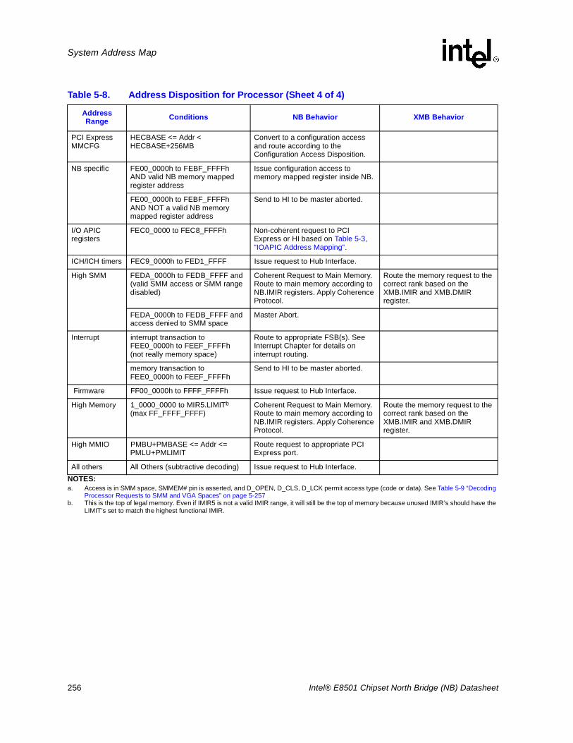
256 Intel® E8501 Chipset North Bridge (NB) Datasheet
System Address Map
PCI Express MMCFG
HECBASE <= Addr < HECBASE+256MB
Convert to a configuration access and route according to the Configuration Access Disposition.
NB specific FE00_0000h to FEBF_FFFFh AND valid NB memory mapped register address
Issue configuration access to memory mapped register inside NB.
FE00_0000h to FEBF_FFFFh AND NOT a valid NB memory mapped register address
Send to HI to be master aborted.
I/O APIC registers
FEC0_0000 to FEC8_FFFFh Non-coherent request to PCI Express or HI based on Table 5-3, “IOAPIC Address Mapping”.
ICH/ICH timers FEC9_0000h to FED1_FFFF Issue request to Hub Interface.
High SMM FEDA_0000h to FEDB_FFFF and(valid SMM access or SMM range disabled)
Coherent Request to Main Memory. Route to main memory according to NB.IMIR registers. Apply Coherence Protocol.
Route the memory request to the correct rank based on the XMB.IMIR and XMB.DMIR register.
FEDA_0000h to FEDB_FFFF and access denied to SMM space
Master Abort.
Interrupt interrupt transaction to FEE0_0000h to FEEF_FFFFh (not really memory space)
Route to appropriate FSB(s). See Interrupt Chapter for details on interrupt routing.
memory transaction to FEE0_0000h to FEEF_FFFFh
Send to HI to be master aborted.
Firmware FF00_0000h to FFFF_FFFFh Issue request to Hub Interface.
High Memory 1_0000_0000 to MIR5.LIMITb
(max FF_FFFF_FFFF)Coherent Request to Main Memory. Route to main memory according to NB.IMIR registers. Apply Coherence Protocol.
Route the memory request to the correct rank based on the XMB.IMIR and XMB.DMIR register.
High MMIO PMBU+PMBASE <= Addr <= PMLU+PMLIMIT
Route request to appropriate PCI Express port.
All others All Others (subtractive decoding) Issue request to Hub Interface.NOTES:a. Access is in SMM space, SMMEM# pin is asserted, and D_OPEN, D_CLS, D_LCK permit access type (code or data). See Table 5-9 “Decoding
Processor Requests to SMM and VGA Spaces” on page 5-257b. This is the top of legal memory. Even if IMIR5 is not a valid IMIR range, it will still be the top of memory because unused IMIR’s should have the
LIMIT’s set to match the highest functional IMIR.
Table 5-8. Address Disposition for Processor (Sheet 4 of 4)
Address Range Conditions NB Behavior XMB Behavior
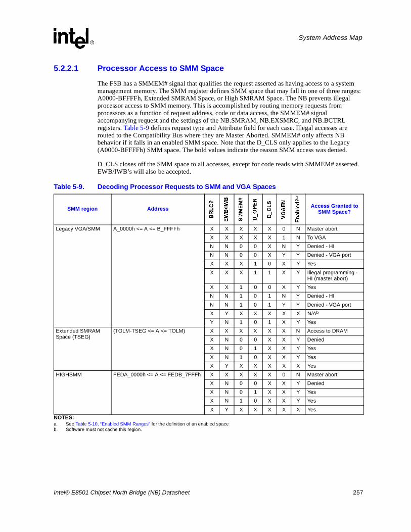
Intel® E8501 Chipset North Bridge (NB) Datasheet 257
System Address Map
5.2.2.1 Processor Access to SMM Space
The FSB has a SMMEM# signal that qualifies the request asserted as having access to a system management memory. The SMM register defines SMM space that may fall in one of three ranges: A0000-BFFFFh, Extended SMRAM Space, or High SMRAM Space. The NB prevents illegal processor access to SMM memory. This is accomplished by routing memory requests from processors as a function of request address, code or data access, the SMMEM# signal accompanying request and the settings of the NB.SMRAM, NB.EXSMRC, and NB.BCTRL registers. Table 5-9 defines request type and Attribute field for each case. Illegal accesses are routed to the Compatibility Bus where they are Master Aborted. SMMEM# only affects NB behavior if it falls in an enabled SMM space. Note that the D_CLS only applies to the Legacy (A0000-BFFFFh) SMM space. The bold values indicate the reason SMM access was denied.
D_CLS closes off the SMM space to all accesses, except for code reads with SMMEM# asserted. EWB/IWB’s will also be accepted.
Table 5-9. Decoding Processor Requests to SMM and VGA Spaces
SMM region Address
NOTES:a. See Table 5-10, “Enabled SMM Ranges” for the definition of an enabled space
Access Granted to SMM Space?
Legacy VGA/SMM A_0000h <= A <= B_FFFFh X X X X X 0 N Master abortX X X X X 1 N To VGAN N 0 0 X N Y Denied - HIN N 0 0 X Y Y Denied - VGA portX X X 1 0 X Y Yes
X X X 1 1 X Y Illegal programming - HI (master abort)
X X 1 0 0 X Y YesN N 1 0 1 N Y Denied - HI
N N 1 0 1 Y Y Denied - VGA portX Y X X X X X N/Ab
b. Software must not cache this region.
Y N 1 0 1 X Y YesExtended SMRAM Space (TSEG)
(TOLM-TSEG <= A <= TOLM) X X X X X X N Access to DRAMX N 0 0 X X Y DeniedX N 0 1 X X Y Yes
X N 1 0 X X Y YesX Y X X X X X Yes
HIGHSMM FEDA_0000h <= A <= FEDB_7FFFh X X X X X 0 N Master abortX N 0 0 X X Y DeniedX N 0 1 X X Y YesX N 1 0 X X Y Yes
X Y X X X X X Yes
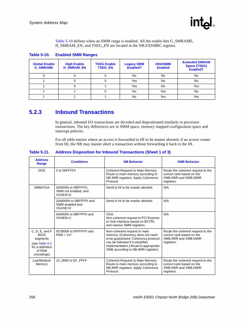
258 Intel® E8501 Chipset North Bridge (NB) Datasheet
System Address Map
Table 5-10 defines when an SMM range is enabled. All the enable bits G_SMRAME, H_SMRAM_EN, and TSEG_EN are located in the NB.EXSMRC register.
5.2.3 Inbound TransactionsIn general, inbound I/O transactions are decoded and dispositioned similarly to processor transactions. The key differences are in SMM space, memory mapped configuration space and interrupt policies.
For all table entries where an access is forwarded to HI to be master aborted, if an access comes from HI, the NB may master abort a transaction without forwarding it back to the HI.
Table 5-10. Enabled SMM Ranges
Global Enable G_SMRAME
High Enable H_SMRAM_EN
TSEG Enable TSEG_EN
Legacy SMM Enabled?
HIGHSMM Enabled
Extended SMRAM Space (TSEG)
Enabled?
0 X X No No No1 0 0 Yes No No1 0 1 Yes No Yes1 1 0 No Yes No1 1 1 No Yes Yes
Table 5-11. Address Disposition for Inbound Transactions (Sheet 1 of 3)
Address Range Conditions NB Behavior XMB Behavior
DOS 0 to 09FFFFh Coherent Request to Main Memory. Route to main memory according to NB.IMIR registers. Apply Coherence Protocol.
Route the coherent request to the correct rank based on the XMB.IMIR and XMB.DMIR registers.
SMM/VGA 0A0000h to 0BFFFFh, SMM not enabled, and VGAEN=0
Send to HI to be master aborted. N/A
(0A0000h to 0BFFFFh and SMM enabled and VGASE=0
Send to HI to be master aborted. N/A
0A0000h to 0BFFFFh andVGAEN=1
VGA:Non-coherent request to PCI Express or Hub Interface based on BCTRL and various SMM registers.
N/A
C, D, E, and F BIOS
segments(see Table 5-1for a definition
of PAM encodings)
0C0000h to 0FFFFFh andPAM = 11a
Non-coherent request to main memory. (Coherency does not need to be guaranteed. Coherency protocol can be followed if it simplifies implementation.) Route to appropriate XMB according to NB.IMIR registers.
Route the coherent request to the correct rank based on the XMB.IMIR and XMB.DMIR registers.
Low/Medium Memory
10_0000 to EF_FFFF Coherent Request to Main Memory. Route to main memory according to NB.IMIR registers. Apply Coherence Protocol.
Route the coherent request to the correct rank based on the XMB.IMIR and XMB.DMIR registers.
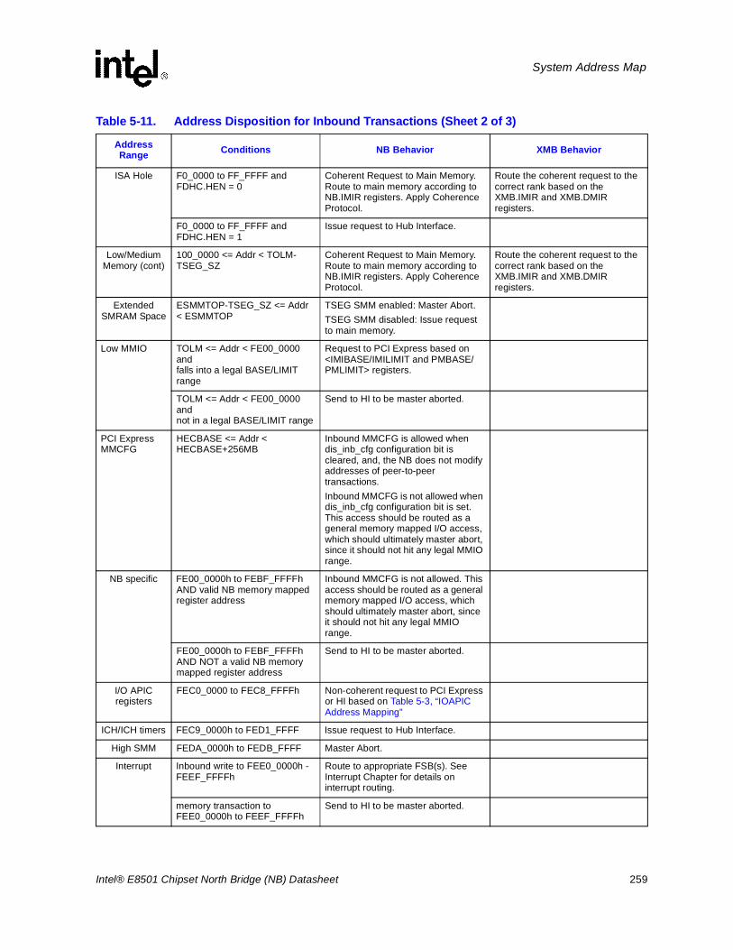
Intel® E8501 Chipset North Bridge (NB) Datasheet 259
System Address Map
ISA Hole F0_0000 to FF_FFFF and FDHC.HEN = 0
Coherent Request to Main Memory. Route to main memory according to NB.IMIR registers. Apply Coherence Protocol.
Route the coherent request to the correct rank based on the XMB.IMIR and XMB.DMIR registers.
F0_0000 to FF_FFFF and FDHC.HEN = 1
Issue request to Hub Interface.
Low/Medium Memory (cont)
100_0000 <= Addr < TOLM-TSEG_SZ
Coherent Request to Main Memory. Route to main memory according to NB.IMIR registers. Apply Coherence Protocol.
Route the coherent request to the correct rank based on the XMB.IMIR and XMB.DMIR registers.
Extended SMRAM Space
ESMMTOP-TSEG_SZ <= Addr < ESMMTOP
TSEG SMM enabled: Master Abort.TSEG SMM disabled: Issue request to main memory.
Low MMIO TOLM <= Addr < FE00_0000 andfalls into a legal BASE/LIMIT range
Request to PCI Express based on <IMIBASE/IMILIMIT and PMBASE/PMLIMIT> registers.
TOLM <= Addr < FE00_0000 andnot in a legal BASE/LIMIT range
Send to HI to be master aborted.
PCI Express MMCFG
HECBASE <= Addr < HECBASE+256MB
Inbound MMCFG is allowed when dis_inb_cfg configuration bit is cleared, and, the NB does not modify addresses of peer-to-peer transactions.Inbound MMCFG is not allowed when dis_inb_cfg configuration bit is set. This access should be routed as a general memory mapped I/O access, which should ultimately master abort, since it should not hit any legal MMIO range.
NB specific FE00_0000h to FEBF_FFFFh AND valid NB memory mapped register address
Inbound MMCFG is not allowed. This access should be routed as a general memory mapped I/O access, which should ultimately master abort, since it should not hit any legal MMIO range.
FE00_0000h to FEBF_FFFFh AND NOT a valid NB memory mapped register address
Send to HI to be master aborted.
I/O APIC registers
FEC0_0000 to FEC8_FFFFh Non-coherent request to PCI Express or HI based on Table 5-3, “IOAPIC Address Mapping”
ICH/ICH timers FEC9_0000h to FED1_FFFF Issue request to Hub Interface.
High SMM FEDA_0000h to FEDB_FFFF Master Abort.
Interrupt Inbound write to FEE0_0000h - FEEF_FFFFh
Route to appropriate FSB(s). See Interrupt Chapter for details on interrupt routing.
memory transaction to FEE0_0000h to FEEF_FFFFh
Send to HI to be master aborted.
Table 5-11. Address Disposition for Inbound Transactions (Sheet 2 of 3)
Address Range Conditions NB Behavior XMB Behavior
260 Intel® E8501 Chipset North Bridge (NB) Datasheet
System Address Map
5.3 I/O Address MapThe I/O address map is separate from the memory map and is primarily used to support legacy code/drivers that use I/O mapped accesses rather than memory mapped I/O accesses. Except for the special addresses listed in Section 5.3.1, “Special I/O Addresses” , I/O accesses are decoded by range and sent to the appropriate HI/PCI Express port, which will route the I/O access to the appropriate device.
5.3.1 Special I/O AddressesThere are two classes of I/O addresses that are specifically decoded by the NB:
• I/O addresses used for VGA controllers.
• I/O addresses used for the PCI Configuration Space Enable (CSE) protocol. The I/O addresses 0CF8h and 0CFCh are specifically decoded as part of the CSE protocol.
Historically, the 64 KB I/O space actually was 64 K+3 bytes. For the extra 3 bytes, A#[16] is asserted. The NB decodes only A#[15:3] when the request encoding indicates an I/O cycle. Therefore accesses with A#[16] asserted are decoded as if they were accesses to address 0 and be forwarded to the Compatibility Bus.
At power-on, all I/O accesses are mapped to the Compatibility Bus.
5.3.2 Outbound I/O AccessThe NB chipset allows I/O addresses to be mapped to resources supported on the I/O buses underneath the NB. This I/O space is partitioned into 32 x 2KB segments. Each of the I/O buses can have from 0 to 32 segments mapped to it. Each PCI bus gets contiguous blocks. All PCI busses must be assigned contiguous blocks. The lowest block, from 0 to 0FFFh, is always sent to the Compatibility Bus. For further details on the legacy I/O ranges that the ICH decodes in the lowest block, please refer to Intel® 82801EB I/O Controller Hub 5 (ICH5) and Intel® 82801ER I/O Controller Hub 5 (ICH5R) Datasheet. The ICH5 Datasheet is available at: http://developer.intel.com/design/chipsets/datashts.
Firmware FF00_0000h to FFFF_FFFFh Master abort.
High Memory 1_0000_0000 to MIR5.LIMIT (max FF_FFFF_FFFF)
Coherent Request to Main Memory. Route to main memory according to NB.IMIR registers. Apply Coherence Protocol.
Route the coherent request to the correct rank based on the XMB.IMIR and XMB.DMIR registers.
High MMIO PMBU+PMBASE <= Addr <= PMLU+PMLIMIT
Route request to appropriate PCI Express port.
All others All Others (subtractive decoding) Issue request to Hub Interface.NOTES:a. Other combinations of PAM’s are not allowed if inbound accesses to this region can occur. Just like Cayuse, chipset functionality is not
guaranteed.
Table 5-11. Address Disposition for Inbound Transactions (Sheet 3 of 3)
Address Range Conditions NB Behavior XMB Behavior
Intel® E8501 Chipset North Bridge (NB) Datasheet 261
System Address Map
5.3.2.1 Outbound I/O Transaction Routing
The NB applies these routing rules in order: (A[2:0] for the following is not physically present on the FSB, but are calculated from BE[7:0]).
1. I/O addresses used for VGA controllers on PCI Express:If one of the BCTRL.VGAEN bit is set, and each addressed byte is in the following range:A[9:0] = 3B0h-3BBh, 3C0h-3DFh. (A[15:10] are ignored for this decode.)The access is sent to the PCI Express port that VGAEN is set for. Note that only one VGAEN bit can be set.For example, a 2 byte read starting at X3BBh includes X3BB-X3BCh (X can be any number since A[15:10] are ignored).Since A[9:0] = 3BCh which is not one of the VGA bytes, the access is not routed to VGA.
2. Configuration accesses: If a request is a DW accesses to 0CF8h (See CFGDAT register) or 1-4 B accesses to 0CFCh with configuration space is enabled (See bit 31 of CFGADR register), the request is considered a configuration access. Configuration accesses are routed based on the bus and device numbers.
3. ISA Aliases: If the BCTRL.ISAEN is set, addresses X100-X3FFh, X500-X7FFh, X900-XBFF, and XD00-XFFFh will result in the access being sent out to the Hub Interface (ICH5). This is the top 768B in each 1KB block.100 =256B 3FF=1K-1
4. I/O defined by IOBASE/IOLIMIT: If PCICMD.IOAE is set in any of the NB PCI Express devices and the I/O address falls in this range: (IOBASE <= address <= IOLIMIT), then the access will be sent to the PCI Express port that is defined by the correct IOBASE/IOLIMIT registers.
5. Otherwise: the I/O Read/Write is sent to HI (ICH5).
Figure 5-7. System I/O Address Space
0000h
Segment 0Compatibility Bus
Only
Segment 1Compatibility Bus
Only
Segment 2
Segment 3
Segment 31
+ 3 bytes(Decoded as 0 000x)
0800h
1000h
1800h
2000h
F800h
FFFFh
1_0002h
262 Intel® E8501 Chipset North Bridge (NB) Datasheet
System Address Map
5.3.3 Inbound I/O AccessesInbound I/O’s are supported only for peer-to-peer accesses and are decoded the same as processor initiated I/O’s. Inbound I/O accesses to the NB (i.e. CF8/CFC) are not supported and will receive a Master Abort response.
§
Intel® E8501 Chipset North Bridge (NB) Datasheet 263
6 Functional Description
This chapter will cover the Intel® E8501 chipset north bridge (NB) functionality and its interface components, including Front Side Bus, IMI, PCI Express and HI1.5. The Intel® E8501 Chipset North Bridge (NB) Datasheet shall only cover the NB component. Details on the rest of the platform components can be found in each component’s respective documentation.
6.1 Processor SupportThe NB is the priority agent for the two FSB’s and is optimized for two 64-bit Intel® Xeon®
Processor MP on each bus. The Intel® E8501 chipset does not allow mixing of 64-bit Intel® Xeon®
processor MP with up to 8MB L3 cache, 64-bit Intel® Xeon® processor MP with 1MB L2 cache or Dual-Core Intel® Xeon® processor 7000 sequence within the same platform.
.
Table 6-1. FSB Feature Summary
Feature Description
Cache Line Size 64B
Clock Rate Control@166 MT/s, Address@333 MT/s, Data@667 MT/s.Control@200 MT/s, Address@400 MT/s, Data@800 MT/s
Addresses NB supports 40 address bits.
Enhanced Defer NB responds using Defer phase when DPS is asserted.
Modified Enhanced Defer NB typically drives IDS# 5 clocks before OOD#.
Maximum Deferred Transactions 32
Maximum In-Order Transactions 12
ECC/Parity NB supports both DEP[7:0]# and DP[3:0]# but not at the same time.
BRIL.OWN NB ignores the OWN bit.
BWLD 64-bit Intel® Xeon® processor MP processors do not issue this trans-action.
BWL.INVLD Disabled and treated as a BWL.
Threads/cores NB fully supports 4 logical agents per FSB.
Modified response following clean snoop (buried HITM)
NB supports this for debug, but not for production. The solution will not be performance optimized. Buried HITM is inconsistent with enhanced defer.
Processor Tristate A[39:36] at reset (see Section 4.14.12, “POC_FSB{A/B}: Power-on Configuration (D16, F0)” on page 168).
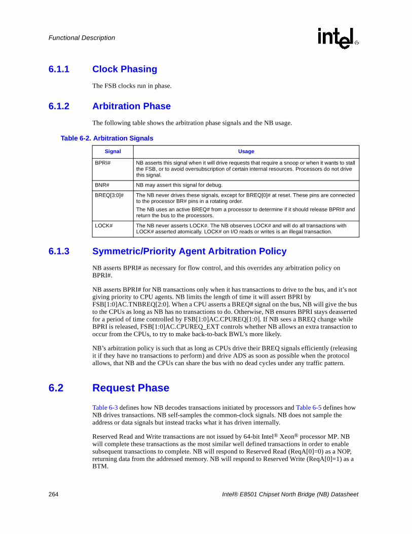
264 Intel® E8501 Chipset North Bridge (NB) Datasheet
Functional Description
6.1.1 Clock PhasingThe FSB clocks run in phase.
6.1.2 Arbitration PhaseThe following table shows the arbitration phase signals and the NB usage.
6.1.3 Symmetric/Priority Agent Arbitration PolicyNB asserts BPRI# as necessary for flow control, and this overrides any arbitration policy on BPRI#.
NB asserts BPRI# for NB transactions only when it has transactions to drive to the bus, and it’s not giving priority to CPU agents. NB limits the length of time it will assert BPRI by FSB[1:0]AC.TNBREQ[2:0]. When a CPU asserts a BREQ# signal on the bus, NB will give the bus to the CPUs as long as NB has no transactions to do. Otherwise, NB ensures BPRI stays deasserted for a period of time controlled by FSB[1:0]AC.CPUREQ[1:0]. If NB sees a BREQ change while BPRI is released, FSB[1:0]AC.CPUREQ_EXT controls whether NB allows an extra transaction to occur from the CPUs, to try to make back-to-back BWL’s more likely.
NB’s arbitration policy is such that as long as CPUs drive their BREQ signals efficiently (releasing it if they have no transactions to perform) and drive ADS as soon as possible when the protocol allows, that NB and the CPUs can share the bus with no dead cycles under any traffic pattern.
6.2 Request PhaseTable 6-3 defines how NB decodes transactions initiated by processors and Table 6-5 defines how NB drives transactions. NB self-samples the common-clock signals. NB does not sample the address or data signals but instead tracks what it has driven internally.
Reserved Read and Write transactions are not issued by 64-bit Intel® Xeon® processor MP. NB will complete these transactions as the most similar well defined transactions in order to enable subsequent transactions to complete. NB will respond to Reserved Read (ReqA[0]=0) as a NOP, returning data from the addressed memory. NB will respond to Reserved Write (ReqA[0]=1) as a BTM.
Table 6-2. Arbitration Signals
Signal Usage
BPRI# NB asserts this signal when it will drive requests that require a snoop or when it wants to stall the FSB, or to avoid oversubscription of certain internal resources. Processors do not drive this signal.
BNR# NB may assert this signal for debug.
BREQ[3:0]# The NB never drives these signals, except for BREQ[0]# at reset. These pins are connected to the processor BR# pins in a rotating order.The NB uses an active BREQ# from a processor to determine if it should release BPRI# and return the bus to the processors.
LOCK# The NB never asserts LOCK#. The NB observes LOCK# and will do all transactions with LOCK# asserted atomically. LOCK# on I/O reads or writes is an illegal transaction.
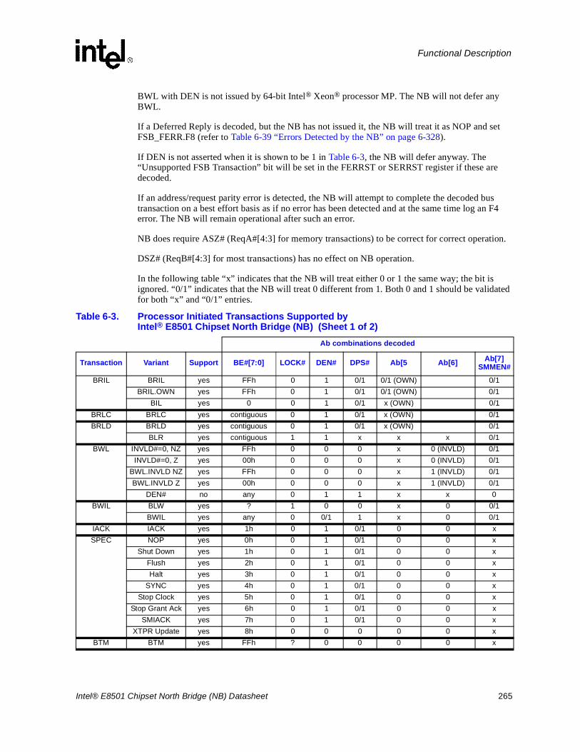
Intel® E8501 Chipset North Bridge (NB) Datasheet 265
Functional Description
BWL with DEN is not issued by 64-bit Intel® Xeon® processor MP. The NB will not defer any BWL.
If a Deferred Reply is decoded, but the NB has not issued it, the NB will treat it as NOP and set FSB_FERR.F8 (refer to Table 6-39 “Errors Detected by the NB” on page 6-328).
If DEN is not asserted when it is shown to be 1 in Table 6-3, the NB will defer anyway. The “Unsupported FSB Transaction” bit will be set in the FERRST or SERRST register if these are decoded.
If an address/request parity error is detected, the NB will attempt to complete the decoded bus transaction on a best effort basis as if no error has been detected and at the same time log an F4 error. The NB will remain operational after such an error.
NB does require ASZ# (ReqA#[4:3] for memory transactions) to be correct for correct operation.
DSZ# (ReqB#[4:3] for most transactions) has no effect on NB operation.
In the following table “x” indicates that the NB will treat either 0 or 1 the same way; the bit is ignored. “0/1” indicates that the NB will treat 0 different from 1. Both 0 and 1 should be validated for both “x” and “0/1” entries.
Table 6-3. Processor Initiated Transactions Supported by Intel® E8501 Chipset North Bridge (NB) (Sheet 1 of 2)
Ab combinations decoded
Transaction Variant Support BE#[7:0] LOCK# DEN# DPS# Ab[5 Ab[6] Ab[7]SMMEN#
BRIL BRIL yes FFh 0 1 0/1 0/1 (OWN) 0/1BRIL.OWN yes FFh 0 1 0/1 0/1 (OWN) 0/1
BIL yes 0 0 1 0/1 x (OWN) 0/1BRLC BRLC yes contiguous 0 1 0/1 x (OWN) 0/1BRLD BRLD yes contiguous 0 1 0/1 x (OWN) 0/1
BLR yes contiguous 1 1 x x x 0/1BWL INVLD#=0, NZ yes FFh 0 0 0 x 0 (INVLD) 0/1
INVLD#=0, Z yes 00h 0 0 0 x 0 (INVLD) 0/1BWL.INVLD NZ yes FFh 0 0 0 x 1 (INVLD) 0/1BWL.INVLD Z yes 00h 0 0 0 x 1 (INVLD) 0/1
DEN# no any 0 1 1 x x 0BWIL BLW yes ? 1 0 0 x 0 0/1
BWIL yes any 0 0/1 1 x 0 0/1IACK IACK yes 1h 0 1 0/1 0 0 xSPEC NOP yes 0h 0 1 0/1 0 0 x
Shut Down yes 1h 0 1 0/1 0 0 xFlush yes 2h 0 1 0/1 0 0 xHalt yes 3h 0 1 0/1 0 0 x
SYNC yes 4h 0 1 0/1 0 0 xStop Clock yes 5h 0 1 0/1 0 0 x
Stop Grant Ack yes 6h 0 1 0/1 0 0 xSMIACK yes 7h 0 1 0/1 0 0 x
XTPR Update yes 8h 0 0 0 0 0 xBTM BTM yes FFh ? 0 0 0 0 x
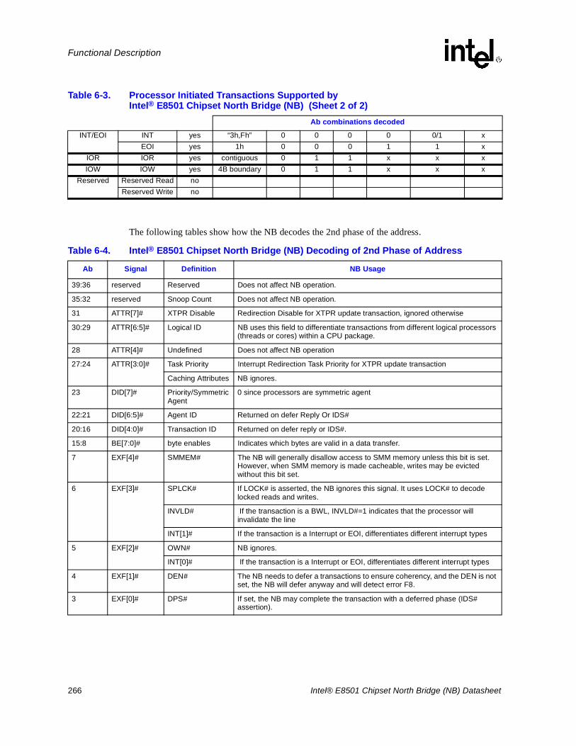
266 Intel® E8501 Chipset North Bridge (NB) Datasheet
Functional Description
The following tables show how the NB decodes the 2nd phase of the address.
INT/EOI INT yes “3h,Fh” 0 0 0 0 0/1 xEOI yes 1h 0 0 0 1 1 x
IOR IOR yes contiguous 0 1 1 x x xIOW IOW yes 4B boundary 0 1 1 x x x
Reserved Reserved Read noReserved Write no
Table 6-3. Processor Initiated Transactions Supported by Intel® E8501 Chipset North Bridge (NB) (Sheet 2 of 2)
Ab combinations decoded
Table 6-4. Intel® E8501 Chipset North Bridge (NB) Decoding of 2nd Phase of Address
Ab Signal Definition NB Usage
39:36 reserved Reserved Does not affect NB operation.
35:32 reserved Snoop Count Does not affect NB operation.
31 ATTR[7]# XTPR Disable Redirection Disable for XTPR update transaction, ignored otherwise
30:29 ATTR[6:5]# Logical ID NB uses this field to differentiate transactions from different logical processors (threads or cores) within a CPU package.
28 ATTR[4]# Undefined Does not affect NB operation
27:24 ATTR[3:0]# Task Priority Interrupt Redirection Task Priority for XTPR update transaction
Caching Attributes NB ignores.
23 DID[7]# Priority/Symmetric Agent
0 since processors are symmetric agent
22:21 DID[6:5]# Agent ID Returned on defer Reply Or IDS#
20:16 DID[4:0]# Transaction ID Returned on defer reply or IDS#.
15:8 BE[7:0]# byte enables Indicates which bytes are valid in a data transfer.
7 EXF[4]# SMMEM# The NB will generally disallow access to SMM memory unless this bit is set. However, when SMM memory is made cacheable, writes may be evicted without this bit set.
6 EXF[3]# SPLCK# If LOCK# is asserted, the NB ignores this signal. It uses LOCK# to decode locked reads and writes.
INVLD# If the transaction is a BWL, INVLD#=1 indicates that the processor will invalidate the line
INT[1]# If the transaction is a Interrupt or EOI, differentiates different interrupt types
5 EXF[2]# OWN# NB ignores.
INT[0]# If the transaction is a Interrupt or EOI, differentiates different interrupt types
4 EXF[1]# DEN# The NB needs to defer a transactions to ensure coherency, and the DEN is not set, the NB will defer anyway and will detect error F8.
3 EXF[0]# DPS# If set, the NB may complete the transaction with a deferred phase (IDS# assertion).
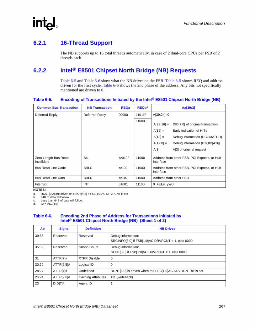
Intel® E8501 Chipset North Bridge (NB) Datasheet 267
Functional Description
6.2.1 16-Thread SupportThe NB supports up to 16 total threads automatically, in case of 2 dual-core CPUs per FSB of 2 threads each.
6.2.2 Intel® E8501 Chipset North Bridge (NB) RequestsTable 6-5 and Table 6-6 show what the NB drives on the FSB. Table 6-5 shows REQ and address driven for the first cycle. Table 6-6 shows the 2nd phase of the address. Any bits not specifically mentioned are driven to 0.
Table 6-5. Encoding of Transactions Initiated by the Intel® E8501 Chipset North Bridge (NB)
Common Bus Transaction NB Transaction REQa REQba
NOTES:a. RCNT[3:2] are driven on REQb[4:3] if FSB[1:0]AC.DRVRCNT is set
Aa[39:3]
Deferred Reply Deferred Reply 00000 11011b
b. 64B of data will follow
A[39:24]=0
11000c
c. Less than 64B of data will follow.
Zero Length Bus Read Invalidate
BIL zz010d
d. zz = ASZ[1:0]
11000 Address from other FSB, PCI Express, or Hub Interface
Bus Read Line Code BRLC zz100 11000 Address from other FSB, PCI Express, or Hub Interface
Bus Read Line Data BRLD zz110 11000 Address from other FSB
Interrupt INT 01001 11100 0_FEEy_yyy0
Table 6-6. Encoding 2nd Phase of Address for Transactions Initiated by Intel® E8501 Chipset North Bridge (NB) (Sheet 1 of 2)
Ab Signal Definition NB Drives
39:36 Reserved Reserved Debug information:SRCINFO[3:0] if FSB[1:0]AC.DRVRCNT = 1, else 0000.
35:32 Reserved Snoop Count Debug information:SCNT[3:0] if FSB[1:0]AC.DRVRCNT = 1, else 0000.
31 ATTR[7]# XTPR Disable 0
30:29 ATTR[6:5]# Logical ID 0
28:27 ATTR[4]# Undefined RCNT[1:0] is driven when the FSB[1:0]AC.DRVRCNT bit is set.
26:24 ATTR[2:0]# Caching Attributes 111 (writeback)
23 DID[7]# Agent ID 1
A[23:16] = DID[7:0] of original transaction
A[15] = Early indication of HIT#
A[13] = Debug information (DBGMATCH)
A[12:8] = Debug information (PTQID[4:0])
A[3] = A[3] of original request
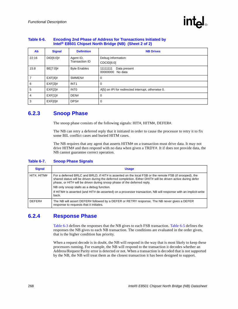
268 Intel® E8501 Chipset North Bridge (NB) Datasheet
Functional Description
6.2.3 Snoop PhaseThe snoop phase consists of the following signals: HIT#, HITM#, DEFER#.
The NB can retry a deferred reply that it initiated in order to cause the processor to retry it to fix some BIL conflict cases and buried HITM cases.
The NB requires that any agent that asserts HITM# on a transaction must drive data. It may not drive HITM# and then respond with no data when given a TRDY#. It if does not provide data, the NB cannot guarantee correct operation.
6.2.4 Response PhaseTable 6-3 defines the responses that the NB gives to each FSB transaction. Table 6-5 defines the responses the NB gives to each NB transaction. The conditions are evaluated in the order given, that is the higher condition has priority.
When a request decode is in doubt, the NB will respond in the way that is most likely to keep these processors running. For example, the NB will respond to the transaction it decodes whether an Address/Request Parity error is detected or not. When a transaction is decoded that is not supported by the NB, the NB will treat them as the closest transaction it has been designed to support.
22:16 DID[6:0]# Agent ID, Transaction ID
Debug information:CDCID[6:0]
15:8 BE[7:0]# Byte Enables 11111111 Data present00000000 No data
7 EXF[4]# SMMEN# 0
6 EXF[3]# INT1 0
5 EXF[2]# INT0 A[5] on IPI for redirected interrupt, otherwise 0.
4 EXF[1]# DEN# 0
3 EXF[0]# DPS# 0
Table 6-6. Encoding 2nd Phase of Address for Transactions Initiated by Intel® E8501 Chipset North Bridge (NB) (Sheet 2 of 2)
Ab Signal Definition NB Drives
Table 6-7. Snoop Phase Signals
Signal Usage
HIT#, HITM# For a deferred BRLC and BRLD, if HIT# is asserted on the local FSB or the remote FSB (if snooped), the shared status will be driven during the deferred completion. Either DHIT# will be driven active during defer phase, or HIT# will be driven during snoop phase of the deferred reply.NB only snoop stalls as a debug function.If HITM# is asserted (and HIT# de-asserted) on a processor transaction, NB will response with an implicit-write back.
DEFER# The NB will assert DEFER# followed by a DEFER or RETRY response. The NB never gives a DEFER response to requests that it initiates.
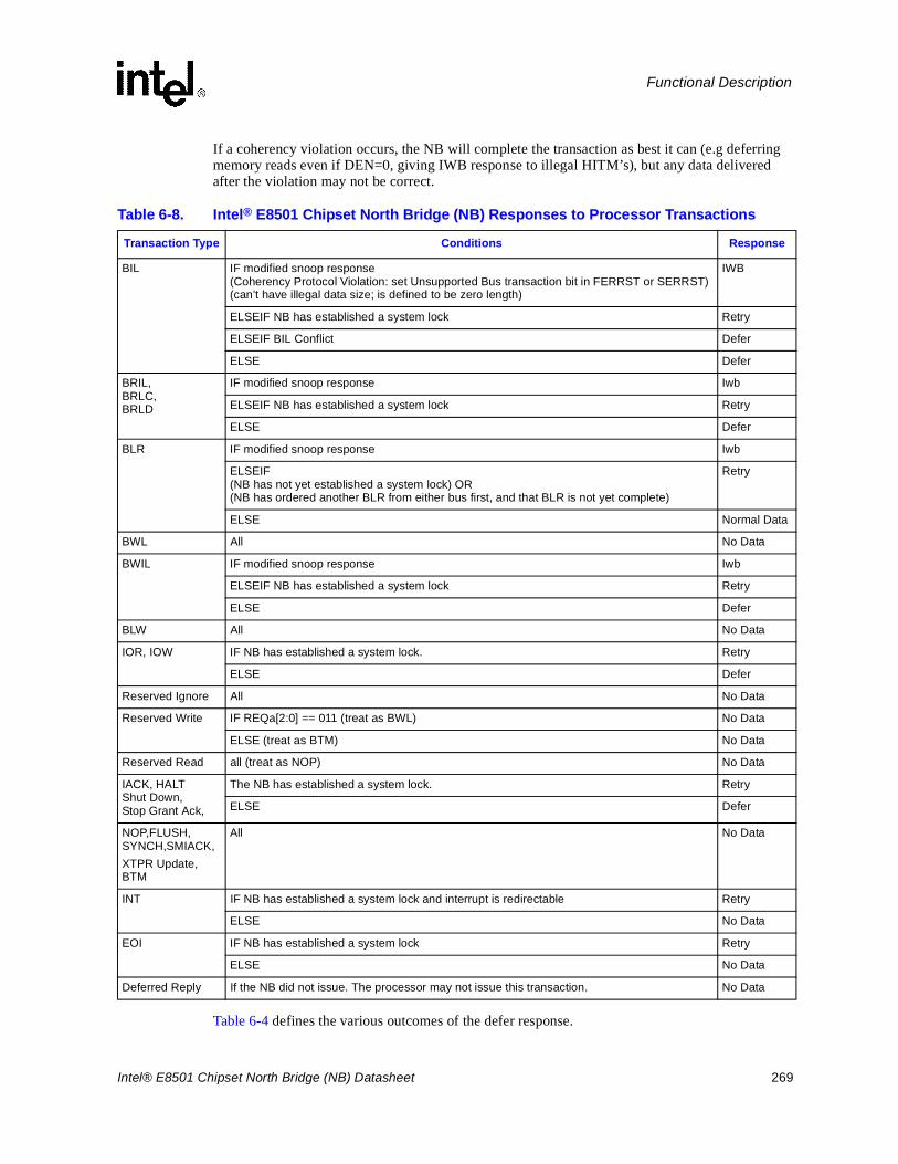
Intel® E8501 Chipset North Bridge (NB) Datasheet 269
Functional Description
If a coherency violation occurs, the NB will complete the transaction as best it can (e.g deferring memory reads even if DEN=0, giving IWB response to illegal HITM’s), but any data delivered after the violation may not be correct.
Table 6-4 defines the various outcomes of the defer response.
Table 6-8. Intel® E8501 Chipset North Bridge (NB) Responses to Processor Transactions
Transaction Type Conditions Response
BIL IF modified snoop response(Coherency Protocol Violation: set Unsupported Bus transaction bit in FERRST or SERRST)(can’t have illegal data size; is defined to be zero length)
IWB
ELSEIF NB has established a system lock Retry
ELSEIF BIL Conflict Defer
ELSE Defer
BRIL,BRLC,BRLD
IF modified snoop response Iwb
ELSEIF NB has established a system lock Retry
ELSE Defer
BLR IF modified snoop response Iwb
ELSEIF(NB has not yet established a system lock) OR(NB has ordered another BLR from either bus first, and that BLR is not yet complete)
Retry
ELSE Normal Data
BWL All No Data
BWIL IF modified snoop response Iwb
ELSEIF NB has established a system lock Retry
ELSE Defer
BLW All No Data
IOR, IOW IF NB has established a system lock. Retry
ELSE Defer
Reserved Ignore All No Data
Reserved Write IF REQa[2:0] == 011 (treat as BWL) No Data
ELSE (treat as BTM) No Data
Reserved Read all (treat as NOP) No Data
IACK, HALTShut Down,Stop Grant Ack,
The NB has established a system lock. Retry
ELSE Defer
NOP,FLUSH,SYNCH,SMIACK,XTPR Update,BTM
All No Data
INT IF NB has established a system lock and interrupt is redirectable Retry
ELSE No Data
EOI IF NB has established a system lock Retry
ELSE No Data
Deferred Reply If the NB did not issue. The processor may not issue this transaction. No Data
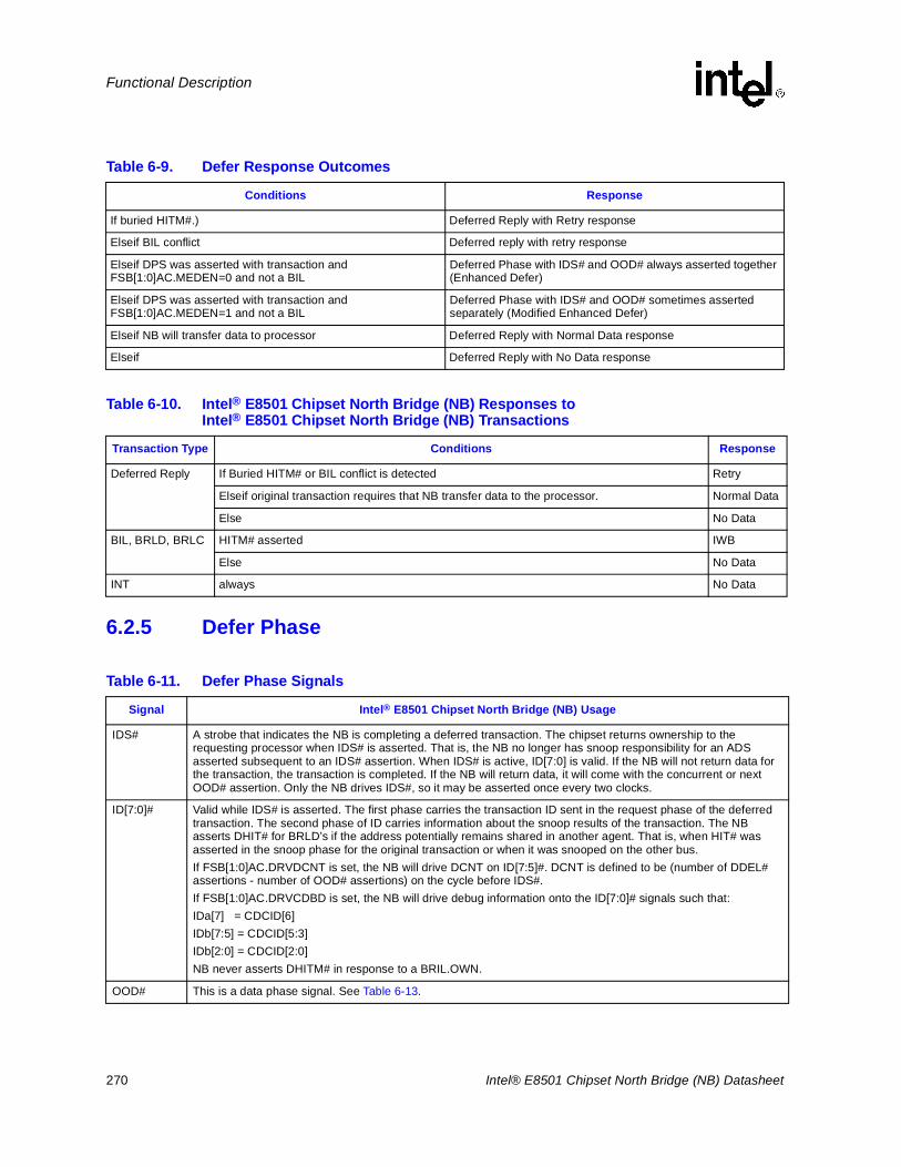
270 Intel® E8501 Chipset North Bridge (NB) Datasheet
Functional Description
.
6.2.5 Defer Phase
Table 6-9. Defer Response Outcomes
Conditions Response
If buried HITM#.) Deferred Reply with Retry response
Elseif BIL conflict Deferred reply with retry response
Elseif DPS was asserted with transaction and FSB[1:0]AC.MEDEN=0 and not a BIL
Deferred Phase with IDS# and OOD# always asserted together (Enhanced Defer)
Elseif DPS was asserted with transaction and FSB[1:0]AC.MEDEN=1 and not a BIL
Deferred Phase with IDS# and OOD# sometimes asserted separately (Modified Enhanced Defer)
Elseif NB will transfer data to processor Deferred Reply with Normal Data response
Elseif Deferred Reply with No Data response
Table 6-10. Intel® E8501 Chipset North Bridge (NB) Responses to Intel® E8501 Chipset North Bridge (NB) Transactions
Transaction Type Conditions Response
Deferred Reply If Buried HITM# or BIL conflict is detected Retry
Elseif original transaction requires that NB transfer data to the processor. Normal Data
Else No Data
BIL, BRLD, BRLC HITM# asserted IWB
Else No Data
INT always No Data
Table 6-11. Defer Phase Signals
Signal Intel® E8501 Chipset North Bridge (NB) Usage
IDS# A strobe that indicates the NB is completing a deferred transaction. The chipset returns ownership to the requesting processor when IDS# is asserted. That is, the NB no longer has snoop responsibility for an ADS asserted subsequent to an IDS# assertion. When IDS# is active, ID[7:0] is valid. If the NB will not return data for the transaction, the transaction is completed. If the NB will return data, it will come with the concurrent or next OOD# assertion. Only the NB drives IDS#, so it may be asserted once every two clocks.
ID[7:0]# Valid while IDS# is asserted. The first phase carries the transaction ID sent in the request phase of the deferred transaction. The second phase of ID carries information about the snoop results of the transaction. The NB asserts DHIT# for BRLD’s if the address potentially remains shared in another agent. That is, when HIT# was asserted in the snoop phase for the original transaction or when it was snooped on the other bus.If FSB[1:0]AC.DRVDCNT is set, the NB will drive DCNT on ID[7:5]#. DCNT is defined to be (number of DDEL# assertions - number of OOD# assertions) on the cycle before IDS#. If FSB[1:0]AC.DRVCDBD is set, the NB will drive debug information onto the ID[7:0]# signals such that:IDa[7] = CDCID[6]IDb[7:5] = CDCID[5:3]IDb[2:0] = CDCID[2:0]NB never asserts DHITM# in response to a BRIL.OWN.
OOD# This is a data phase signal. See Table 6-13.
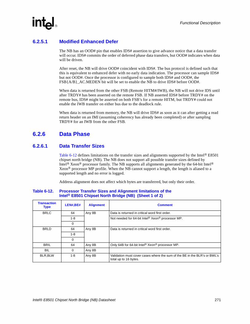
Intel® E8501 Chipset North Bridge (NB) Datasheet 271
Functional Description
6.2.5.1 Modified Enhanced Defer
The NB has an OOD# pin that enables IDS# assertion to give advance notice that a data transfer will occur. IDS# commits the order of deferred phase data transfers, but OOD# indicates when data will be driven.
After reset, the NB will drive OOD# coincident with IDS#. The bus protocol is defined such that this is equivalent to enhanced defer with no early data indication. The processor can sample IDS# but not OOD#. Once the processor is configured to sample both IDS# and OOD#, the FSB{A/B}_AC.MEDEN bit will be set to enable the NB to drive IDS# before OOD#.
When data is returned from the other FSB (Remote HITM#/IWB), the NB will not drive IDS until after TRDY# has been asserted on the remote FSB. If NB asserted IDS# before TRDY# on the remote bus, IDS# might be asserted on both FSB’s for a remote HITM, but TRDY# could not enable the IWB transfer on either bus due to the deadlock rule.
When data is returned from memory, the NB will drive IDS# as soon as it can after getting a read return header on an IMI (assuming coherency has already been completed) or after sampling TRDY# for an IWB from the other FSB.
6.2.6 Data Phase
6.2.6.1 Data Transfer Sizes
Table 6-12 defines limitations on the transfer sizes and alignments supported by the Intel® E8501 chipset north bridge (NB). The NB does not support all possible transfer sizes defined by Intel® Xeon® processor family. The NB supports all alignments generated by the 64-bit Intel®Xeon® processor MP profile. When the NB cannot support a length, the length is aliased to a supported length and no error is logged.
Address alignment does not affect which bytes are transferred, but only their order.
Table 6-12. Processor Transfer Sizes and Alignment limitations of the Intel® E8501 Chipset North Bridge (NB) (Sheet 1 of 2)
Transaction Type LEN#,BE# Alignment Comment
BRLC 64 Any 8B Data is returned in critical word first order.
1-8 Not needed for 64-bit Intel® Xeon® processor MP.0
BRLD 64 Any 8B Data is returned in critical word first order.1-8
0BRIL 64 Any 8B Only 64B for 64-bit Intel® Xeon® processor MP.
BIL 0 Any 8B BLR,BLW 1-8 Any 8B Validation must cover cases where the sum of the BE in the BLR’s or BWL’s
total up to 16 bytes.
272 Intel® E8501 Chipset North Bridge (NB) Datasheet
Functional Description
6.2.6.2 Data Transfer Signals
Table 6-13 shows the signals used for data transfers.
BWIL 64 Any 8B Data is received in critical word first order
1-8 Any combination of byte enables are legal. The BE do not need to be contiguous and any number from 0-8 may be asserted. For example, patterns such as 0001_1111, 0001_0101, 0101_0101 or 1010_1111 are allowed.Note: Downstream devices may not be able to support these unrestricted patterns of BE if the address maps to a MMCFG region.
0 NB will assert TRDY for memory writes with zero data length but the processor will not assert any data transfer signals.
BWL 64B Any 8B NB will assert TRDY for memory writes with zero data length but the processor will not assert any data transfer signals.0
I/O read 1-4 byte Any 8B the NB ignores the LEN field. Therefore, if LEN is other than “8 bytes or less” the transaction will be handled as usual and no error will be detected.
I/O write 1-4 byte Any 8B the NB ignores the LEN field. Therefore, if LEN is other than “8 bytes or less” the transaction will be handled as usual and no error will be detected.BE may NOT cross 4B boundary.
IACK n/a n/a Reqb[2:0] =000, Address ignored.SPEC n/a n/a Reqb[2:0] =001, Address ignored.BTM n/a n/a Reqb[2:0] =000, Address ignored.INT 2B or 4B n/a Address field holds other information.EOI 1B n/a Address is meaningless.
XTPR_UPDATE ? n/a Address is meaningless.
Table 6-12. Processor Transfer Sizes and Alignment limitations of the Intel® E8501 Chipset North Bridge (NB) (Sheet 2 of 2)
Transaction Type LEN#,BE# Alignment Comment
Table 6-13. Data Transfer Signals (Sheet 1 of 2)
Signal NB Usage
H_{A/B}_TRDY# Signals that a symmetric agent may transfer either Write or Implicit-Writeback data.
H_{A/B}_DBSY# The data bus is owned by some agent that cycle. Does not imply that data is necessarily being transferred that cycle.
H_{A/B}_DRDY# data is valid. NB asserts for read data.
H_{A/B}_D[63:0]# 64 bits of data transferred at 4x the bus clock frequency.
H_{A/B}_DEP[7:0]# ECC coverage over D[63:0]. Transferred at 4x the bus clock frequency.
H_{A/B}_DP[3:0]# Odd parity over DBI and D[63:0].DP must be disabled if DEP is used.
Intel® E8501 Chipset North Bridge (NB) Datasheet 273
Functional Description
6.2.7 Error SignalsThe NB observes BINIT# and can be configured to drive BINIT# in certain error situations, including propagating BINIT# to the other FSB.
The “observed BINIT#” bit will be set in the FERR register and this may be configured to reset the system via ICHRST#.
The NB can be configured to assert MCERR# on the other bus when a processor asserts MCERR# (see Section 4.16.21).
6.2.8 Bus Assumptions • BRLC’s and BRLD’s from the processor that have no BE asserted will get a No-Data
Response. A PCI Express or Hub Interface request will be issued, but there are configuration bits to drop these zero length transactions in the I/O subsystem of NB.
• A locked request that is retried by the NB must be reissued unless a fatal processor error occurs.
6.2.9 FSB Coherency AssumptionsThe following line state assumptions can be made following the snoop phase of a given transaction on a FSB populated with fully enabled 64-bit Intel® Xeon® processor MP.
H_{A/B}_DBI[3:0]# Each DBI bit is associated with 16 data lines and 2 ECC lines. If most of any of the 18 bits in a group are active, the NB inverts the group and the corresponding DBI bit is set. Note that DBI will cover all quad pumped signals including DEP. Transferred at 4x the bus clock frequency.
H_{A/B}_OOD# Indicates that the next or concurrent data transfer will be for deferred phase data delivery.
H_{A/B}_DSTBp#[3:0],H_{A/B}_DSTBn#[3:0]
Strobes for D[63:0]#, DEP[7:0]# and DBI[3:0]#.
Table 6-13. Data Transfer Signals (Sheet 2 of 2)
Signal NB Usage
Table 6-14. 64-bit Intel® Xeon® Processor MP FSB Coherency Assumptions (Sheet 1 of 2)
Possible Bus States after Snoop
Transactiontype
Snoop Result = Modifieda Snoop Result = Sharedb Snoop Result = Cleanc
Processor Initiated BRLC SI SI MESI
NB initiated BRLC I SI SId
Processor Initiated BRLD MESI SI MESI
NB initiated BRLD I SI I
BRIL.OWN M Can't Happene MESI
BRIL MESI Can't Happen MESI
Processor Initiated BIL Can’t Happenf
274 Intel® E8501 Chipset North Bridge (NB) Datasheet
Functional Description
6.2.10 Power-on Configuration
6.2.10.1 POC Register
If a bit is set in the POC register, it will drive the corresponding address line during reset. See Section 4.14.12, “POC_FSB{A/B}: Power-on Configuration (D16, F0)” on page 168 and Section 4.14.13, “POC_AUX{A/B}: CPU Tristate Control (D16, F0)” on page 170 for the register definition. This includes processor tristate on A[39:36].
6.2.10.2 BREQ0
The NB asserts BREQ[0]# during RESET# on each bus to enable processors to determine their AgentID. In a configuration with 2 processor sockets on each bus, BREQ[0]# should be routed to BREQ[0]# on the first socket (end agent) and BREQ[1]# of the second socket (Middle agent) of each bus so that they use AgentID 0 and 1 on each FSB.
6.2.10.3 Pins that Do Not Connect to NB
The NB does not connect to A20M#, PMI#, SLPCK#, IGNNE#, IERR#, SMI# or STPCLK#.
6.3 Independent Memory Interface (IMI)
6.3.1 TopologyThe NB masters 1 to 4 Independent Memory Interface (IMI) Ports, each of which is connects to one XMB. The IMI’s are half-width (one byte of payload/transfer) outbound and full-width (2 Bytes of payload/transfer) inbound. Each IMI supports up to 1 Terabyte (240 Bytes) of addressability. The IMI’s are operated independently, that is a given cache line request is serviced by 1 IMI. The NB does not support cascaded, or lock-stepped IMI’s.
NB initiated BIL I Can't Happen I
BWL INVLD=0 Can’t Happen, not snooped MESIg
BWL INVLD=1 Can’t Happen, not snooped I
BWIL I Can't Happen I
BLR SI SI SI
BLW Can’t happenh I I
NOTES:a. HIT# = 0, HITM# = 1. Some agent currently has the line in modified state, but will reduce to shared or invalidb. HIT# = 1, HITM# = 0. Some agent intends to keep the line in shared statec. HIT# = 0, HITM# = 0. The line is invalid in all processor cachesd. The shared result is only possible when 64-bit Intel® Xeon® processor MP L2 is disabled. The NB will assume I when the CDCC.BRLCI bit is set.
This should typically be set. e. A shared response indicates the agent intends to keep the line in shared state which is illegal for an Invalidating transactionf. The 64-bit Intel® Xeon® processor MP does not issue BIL, even when L2 is disabled. It will back invalidate BIL’s from Prescott on the IFSBg. If attribute was WC, NB could assume I, but NB does not use attributes for coherency assumptionsh. Must be preceded by a BLR that would invalidate
Table 6-14. 64-bit Intel® Xeon® Processor MP FSB Coherency Assumptions (Sheet 2 of 2)
Possible Bus States after Snoop
Intel® E8501 Chipset North Bridge (NB) Datasheet 275
Functional Description
6.3.2 Physical LayerThe physical layer will be based on Scalable Differential electricals. As mentioned above, the NB issues half-width packets outbound and full-width packets inbound. The returning inbound link must be the same frequency and generated from the same clock buffer. This allows NB to perform bit de-skewing once at reset rather than periodically.
The NB drives the IMI outbound at 2.67 GHz or 3.2 GHz (16 times the front side bus clock rate). Since an outbound packet takes 8 transfers, commands can be issued at 333 MHz or 400 MHz. A single Write command transfer takes 9 packets, so writes can be issued at 167 MHz or 200 MHz.
The NB can accept responses inbound at the same rate as the outbound (2.67 GHz or 3.2 GHz). Since the inbound data packet is 4 transfers, the NB can accept one-read returns from each IMI at 667 MHz or 800 MHz. Write acknowledges are accepted at 333 MHz or 400 MHz.
6.3.3 Memory SpaceMemRds and MemWrs are issued to memory space. The IMI has more address bits than the FSB’s, so NB IMI addresses will be the same as FSB, PCI Express or HI1.5 addresses. NB will always drive Mem_Address[41:40] to zero in IMI packets.
The NB has a set of IMI Interleave Range (IMIR) registers which define the IMI to which a memory request should be issued (Section 4.15.15, “IMIR[5:0]: IMI Interleave Range, (D16, F1)” on page 188). The IMIR registers partition the memory address space at 256 MB boundaries. Within each IMI Interleave Range, cache lines may be interleaved in different ways to support optimum interleaving of arbitrary (non-symmetrical) memory populations.
6.3.4 Configuration SpaceNB issues ConfigWrs and ConfigRds to Configuration space. Only one Configuration Space access can be outstanding on the IMI at a time. Configuration accesses are limited to 1, 2 or 4 bytes in size. Any combination of contiguous Byte enables is supported.
6.3.4.1 Device Assignment
The NB assigns device numbers to the 4 IMI’s and their corresponding XMBs as described in Table 4-8 on page 60. These all appear on Bus 0.
The XMBDEV register defines the XMB device used for each IMI. They will default to the correct fixed values for the attached XMBs so that BIOS need not perform any enumeration. NB BIOS should not modify these registers, and does not need to read them. The only usage of these registers is for non-NB specific software (e.g. Hot-Plug driver) to determine the device number of an XMB attached to a IMI.
The NB does not support cascaded XMBs, which would require multiple devices.
The IMI requires that the NB toggle a bit in the header for each configuration access so that the NB can distinguish a new command from a retry. The IMI allows only one configuration command outstanding at a time.
276 Intel® E8501 Chipset North Bridge (NB) Datasheet
Functional Description
Normally, the NB responds to XMB configuration requests for register offsets < 40h whether the XMB is present or not. Most of these registers are read-only so any IMI function can be accessed to provide the data. The NB will return the XMB value for the DID register. The SVID registers are writable once, so it is possible that software could write these registers. The NB maintains separate SID and SVID registers for the XMB functions. When the IMIHPC.XMBHDR bit is set, the NB forwards the accesses to the XMB to allow examination of the revision ID of the XMB.
The NB will master-abort any configuration requests to the XMB when the corresponding IMI is in a state that does not support XMB configuration accesses.
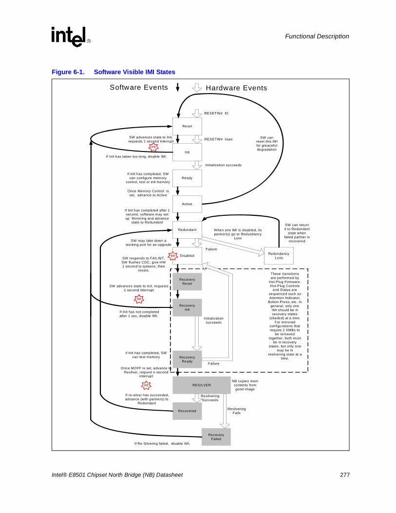
Intel® E8501 Chipset North Bridge (NB) Datasheet 277
Functional Description
Figure 6-1. Software Visible IMI States
Reset
RESETIN# rises
RESETIN# lO
Init
Active
Redundant
Disabled
When one IMI is disabled, itspartner(s) go to Redundancy
Loss
Int
SW advances state to Init,requests 1 second interrupt
If Init has completed after 1second, software may setup Mirroring and advance
state to Redundant
SW responds to FAILINT,SW flushes CDC, give HW1 second to quiesce, then
resets.
RecoveryReset
Initialization succeeds
Int
If Init has taken too long, disable IMI.
Int
if Init has not completedafter 1 sec, disable IMI.
Initializationsucceeds
Failure
if Init has completed, SWcan test memory
RESILVERNB copies memcontents fromgood image
ResilveringSucceeds
RecoveryFailed
Recovered ResilveringFails
Once MOFF is set, advance toResilver, request n second
interrupt
If re-silver has succeeded,advance (with partners) to
Redundant
If Re-Silvering failed, disable IMI.
Software Events Hardware Events
SW may take down aworking port for an upgrade
Int
RedundancyLoss
SW can returnit to Redundant
state whenfailed partner is
recovered
SW canreset this IMIfor greacefuldegradation
These transitionsare performed by
Hot-Plug Firmware.Hot-Plug Controls
and Status aresequenced such asAttention Indicator,
Button Press, etc. Ingeneral, only oneIMI should be inrecovery states
(shaded) at a time.For mirrored
configurations thatrequire 2 XMBs to
be removedtogether, both must
be in recoverystates, but only one
may be inresilvering state at a
time.
Failure
ReadyIf Init has completed, SW
can configure memorycontrol, test or init memory
SW advances state to Init, requests1 second interrupt
Once Memory Control isset, advance to Active
RecoveryInit
RecoveryReady
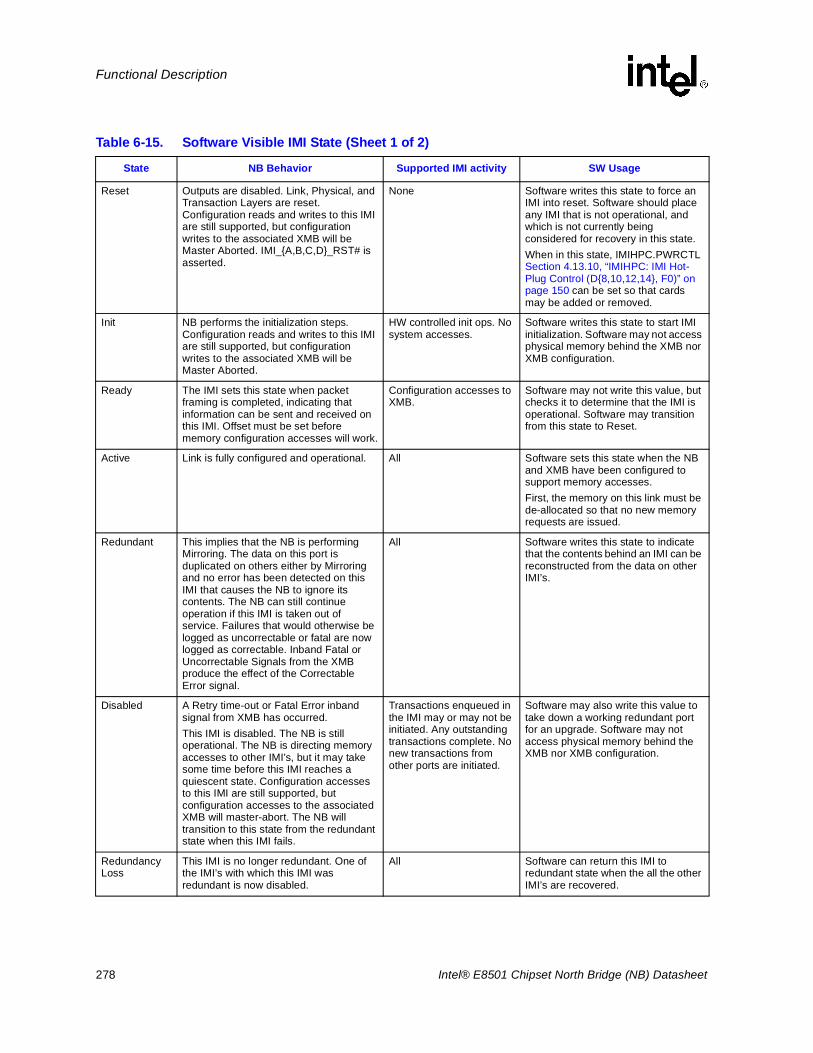
278 Intel® E8501 Chipset North Bridge (NB) Datasheet
Functional Description
Table 6-15. Software Visible IMI State (Sheet 1 of 2)
State NB Behavior Supported IMI activity SW Usage
Reset Outputs are disabled. Link, Physical, and Transaction Layers are reset. Configuration reads and writes to this IMI are still supported, but configuration writes to the associated XMB will be Master Aborted. IMI_{A,B,C,D}_RST# is asserted.
None Software writes this state to force an IMI into reset. Software should place any IMI that is not operational, and which is not currently being considered for recovery in this state.When in this state, IMIHPC.PWRCTL Section 4.13.10, “IMIHPC: IMI Hot-Plug Control (D{8,10,12,14}, F0)” on page 150 can be set so that cards may be added or removed.
Init NB performs the initialization steps. Configuration reads and writes to this IMI are still supported, but configuration writes to the associated XMB will be Master Aborted.
HW controlled init ops. No system accesses.
Software writes this state to start IMI initialization. Software may not access physical memory behind the XMB nor XMB configuration.
Ready The IMI sets this state when packet framing is completed, indicating that information can be sent and received on this IMI. Offset must be set before memory configuration accesses will work.
Configuration accesses to XMB.
Software may not write this value, but checks it to determine that the IMI is operational. Software may transition from this state to Reset.
Active Link is fully configured and operational. All Software sets this state when the NB and XMB have been configured to support memory accesses. First, the memory on this link must be de-allocated so that no new memory requests are issued.
Redundant This implies that the NB is performing Mirroring. The data on this port is duplicated on others either by Mirroring and no error has been detected on this IMI that causes the NB to ignore its contents. The NB can still continue operation if this IMI is taken out of service. Failures that would otherwise be logged as uncorrectable or fatal are now logged as correctable. Inband Fatal or Uncorrectable Signals from the XMB produce the effect of the Correctable Error signal.
All Software writes this state to indicate that the contents behind an IMI can be reconstructed from the data on other IMI’s.
Disabled A Retry time-out or Fatal Error inband signal from XMB has occurred. This IMI is disabled. The NB is still operational. The NB is directing memory accesses to other IMI’s, but it may take some time before this IMI reaches a quiescent state. Configuration accesses to this IMI are still supported, but configuration accesses to the associated XMB will master-abort. The NB will transition to this state from the redundant state when this IMI fails.
Transactions enqueued in the IMI may or may not be initiated. Any outstanding transactions complete. No new transactions from other ports are initiated.
Software may also write this value to take down a working redundant port for an upgrade. Software may not access physical memory behind the XMB nor XMB configuration.
Redundancy Loss
This IMI is no longer redundant. One of the IMI’s with which this IMI was redundant is now disabled.
All Software can return this IMI to redundant state when the all the other IMI’s are recovered.
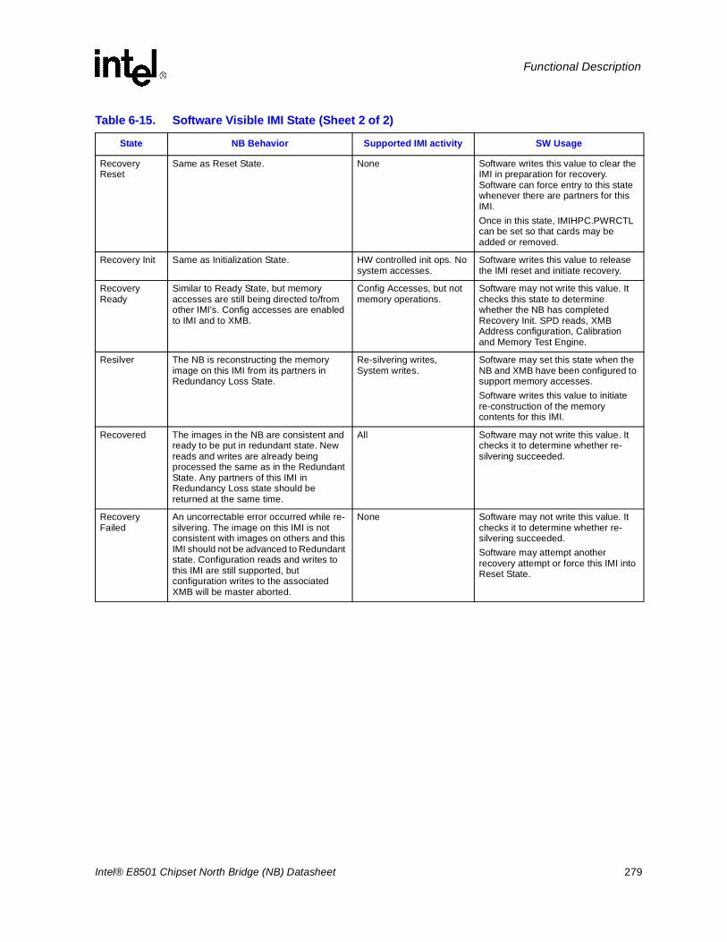
Intel® E8501 Chipset North Bridge (NB) Datasheet 279
Functional Description
Recovery Reset
Same as Reset State. None Software writes this value to clear the IMI in preparation for recovery. Software can force entry to this state whenever there are partners for this IMI.Once in this state, IMIHPC.PWRCTL can be set so that cards may be added or removed.
Recovery Init Same as Initialization State. HW controlled init ops. No system accesses.
Software writes this value to release the IMI reset and initiate recovery.
Recovery Ready
Similar to Ready State, but memory accesses are still being directed to/from other IMI’s. Config accesses are enabled to IMI and to XMB.
Config Accesses, but not memory operations.
Software may not write this value. It checks this state to determine whether the NB has completed Recovery Init. SPD reads, XMB Address configuration, Calibration and Memory Test Engine.
Resilver The NB is reconstructing the memory image on this IMI from its partners in Redundancy Loss State.
Re-silvering writes, System writes.
Software may set this state when the NB and XMB have been configured to support memory accesses. Software writes this value to initiate re-construction of the memory contents for this IMI.
Recovered The images in the NB are consistent and ready to be put in redundant state. New reads and writes are already being processed the same as in the Redundant State. Any partners of this IMI in Redundancy Loss state should be returned at the same time.
All Software may not write this value. It checks it to determine whether re-silvering succeeded.
Recovery Failed
An uncorrectable error occurred while re-silvering. The image on this IMI is not consistent with images on others and this IMI should not be advanced to Redundant state. Configuration reads and writes to this IMI are still supported, but configuration writes to the associated XMB will be master aborted.
None Software may not write this value. It checks it to determine whether re-silvering succeeded.Software may attempt another recovery attempt or force this IMI into Reset State.
Table 6-15. Software Visible IMI State (Sheet 2 of 2)
State NB Behavior Supported IMI activity SW Usage
280 Intel® E8501 Chipset North Bridge (NB) Datasheet
Functional Description
6.3.5 Memory RAS
6.3.5.1 Memory Mirroring
In the mirrored configuration, one of the IMI ports will be designated the primary image and the other the secondary (for an overview on mirroring, refer to Section 2.6.3). Both ports will be issued the same write request and both ports will respond to the request (in a ping-pong fashion). The primary designation will toggle between the two IMI ports on detected correctable memory responses. The primary designation will become fixed on a specific port on an uncorrectable error.
Memory Mirroring Write Operation- For the case of memory writes, the write request is issued to both IMI ports. The NB must successfully collect both responses before considering the write completion. If the write request fails on an IMI port, the write will be re-issued to both ports with exactly the same transaction ID. If the retried write is acknowledged by only one port, switch to the single image (no mirror available).
Memory Mirroring Read Operation- For the case of memory reads, the read request does not go to both mirrors. At the successful completion of the read response, the read response is allowed to complete on the front side bus, PCI Express or HI1.5 interface.
In the case of a detected error, the action of the NB is as follows:
• In the case of a detected Correctable Error, the definition of the Primary image will toggle and the read will be issued on the “new” primary image.
• In the case of a detected Uncorrectable Error, the definition of the Primary image will “hard fail” to the other image. In this case, the “failed” image will never become primary until service has replaced the FRU (Field Replaceable Units) and “re-silvered” the images.
In the event of a switch between the primary and secondary port designations, the NB will ensure that the IMI ports are idle at the time of the switch.
Copy Engine (re-silvering the images) - In the event that the memory configuration has changed (as when a failed memory FRU has been replaced), the NB uses a copy engine to walk memory from the primary image and write it back to both ports. When the copy engine is enabled, all writes are issued to both ports.
The steps to copy (or re-silver two memory images) are as follows:
1. IMI Link goes through a training and initialization process.
2. XMB registers are initialized.
3. Memory behind the XMB is tested and initialized (“0” is written with valid ECC).
4. NB copy engine is enabled. At this time writes start being issued to both images.
5. When copy is completed, re-enable mirroring. (i.e. Failures of the primary memory image are no longer FATAL errors).
Intel® E8501 Chipset North Bridge (NB) Datasheet 281
Functional Description
Correctable Errors - The NB will just correct the data and provide to the requester. The XMB will also correct the data and write back into memory.
Reasons to degrade to one memory image:
• Receiving two uncorrectable errors (not including poisoned data) for the same access.
• Receiving Fatal Error Signal from an XMB.
• Software disabling an IMI interface.
Re-enabling of memory mirroring:
• Replacement of a Failed Memory FRU via the Hot-Plug procedure.
• Software/Firmware will configure and test a memory card FRU. If the memory card matches in size with the current image, the re-silvering process can be enabled. Upon successful completion of the copying process, the two images can be re-enabled.
6.3.5.2 Memory RAID
Memory RAID Read Operation
Normal Case - Read Requests for a given Cache Line can be issued just as in the normal memory configuration to a given address with the following changes:
• RAID Address decoding must be done to route to the appropriate IMI Port.
• Address conflict check logic must take into account not only an address match for a write in progress, but also an address match of the Memory RAID associative lines. As indicated in Table 6-16, a read of “Cache Line 0” must be delayed to occur after any of the following writes of Cache Line 0.
Reconstructive Case - In the case of a failed IMI port, there are two cases for reading a cache line (for this discussion, we assume that IMI Port D has failed):
• To read Cache Line 0, the NB performs a normal read.
• To read Cache Line 2n (for example when IMI Port D is failed), is to read checkline(2n, n, 0), cache line n and cache line 0 and re-construct cache line 2n, as in the following equation:
Memory RAID Write Operation
Normal Case - Write Request for a given cache line requires the cache line to be written and the check line to be updated accordingly. The steps of the write of cache line 0 are as follows:
1. Read Cache Line 2n and n.
2. Calculate Checkline, which is the exclusive OR of cache line 0, n, 2n.
3. Write Cache Line 0 and Check Line (2n,n,0).
cacheline 2n checkline cacheline n cacheline 0=
282 Intel® E8501 Chipset North Bridge (NB) Datasheet
Functional Description
Reconstructive Case - In the case of a failed IMI port, there are two cases for writing a cache line (for this discussion, we assume that IMI Port D has failed):
• To write Cache Line 0, the NB must read its checkline and cacheline 0 (old value); recalculate checkline, write new value of checkline and cacheline0. The calculation of the checkline is as follows:
• To write Cache Line 2 (assuming that IMI Port D is failed), is to update the checkline(2n+2,n+2, 2):
Memory RAID Re-silvering Operation
The re-silvering process for Memory RAID requires the NB to read from the other three IMI ports, regenerate the failed IMI Link data and then write the reconstructed data back. To reconstruct the failed IMI (for this example, IMI port D is being re-silvered), use the following equation:
Note: As in the Memory Mirroring Case, all write operations must also happen to maintain cache coherency of the platform.
When the RAID re-silvering reaches terminal count, the re-silver link is available for normal operation. The size of the re-silvering is determined by the base and size programmed in IMIR3.
Cache Line Striping
For Memory RAID, the NB will use all four IMI Ports and provide a check cache line for every three cache lines. Table 6-16 describes how the IMI ports stripe the cache line. Also note the “n” in the table is equal to a fourth of all the memory available in the platform. For example, if a platform had 16GB of memory, “n” = 4 GB, 12 GB would be used as system address space and 4 GB is used for “Check lines”.
checkline new chechkline old cacheline0 old cacheline0 new=
checkline 2n 2 n 2 2++ cacheline 2n 2+ cacheline n 2+ cacheline 2 new=
IMID IMIC IMIB IMIA=
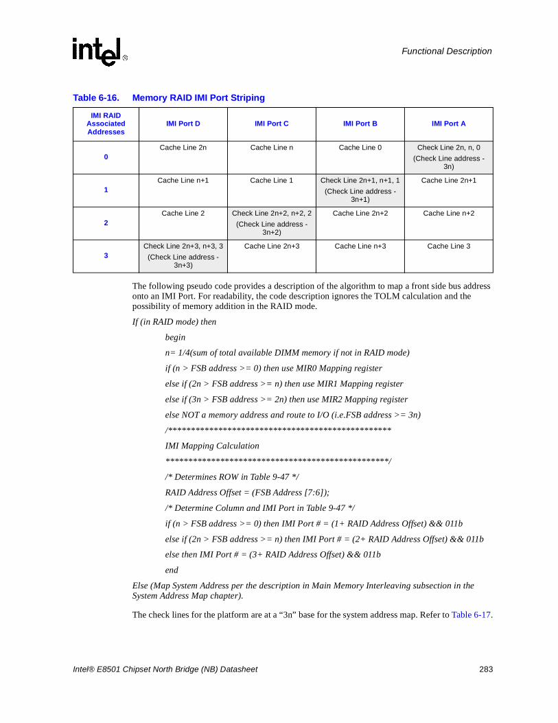
Intel® E8501 Chipset North Bridge (NB) Datasheet 283
Functional Description
The following pseudo code provides a description of the algorithm to map a front side bus address onto an IMI Port. For readability, the code description ignores the TOLM calculation and the possibility of memory addition in the RAID mode.
If (in RAID mode) then
begin
n= 1/4(sum of total available DIMM memory if not in RAID mode)
if (n > FSB address >= 0) then use MIR0 Mapping register
else if (2n > FSB address >= n) then use MIR1 Mapping register
else if (3n > FSB address >= 2n) then use MIR2 Mapping register
else NOT a memory address and route to I/O (i.e.FSB address >= 3n)
/*************************************************
IMI Mapping Calculation
*************************************************/
/* Determines ROW in Table 9-47 */
RAID Address Offset = (FSB Address [7:6]);
/* Determine Column and IMI Port in Table 9-47 */
if (n > FSB address >= 0) then IMI Port # = (1+ RAID Address Offset) && 011b
else if (2n > FSB address >= n) then IMI Port # = (2+ RAID Address Offset) && 011b
else then IMI Port # = (3+ RAID Address Offset) && 011b
end
Else (Map System Address per the description in Main Memory Interleaving subsection in the System Address Map chapter).
The check lines for the platform are at a “3n” base for the system address map. Refer to Table 6-17.
Table 6-16. Memory RAID IMI Port Striping
IMI RAID Associated Addresses
IMI Port D IMI Port C IMI Port B IMI Port A
0Cache Line 2n Cache Line n Cache Line 0 Check Line 2n, n, 0
(Check Line address - 3n)
1Cache Line n+1 Cache Line 1 Check Line 2n+1, n+1, 1
(Check Line address - 3n+1)
Cache Line 2n+1
2Cache Line 2 Check Line 2n+2, n+2, 2
(Check Line address - 3n+2)
Cache Line 2n+2 Cache Line n+2
3Check Line 2n+3, n+3, 3
(Check Line address - 3n+3)
Cache Line 2n+3 Cache Line n+3 Cache Line 3
284 Intel® E8501 Chipset North Bridge (NB) Datasheet
Functional Description
Memory Upgrade Support for the Memory RAID
The NB/XMB provide the ability to allow memory upgrade operations while in the RAID configurations. To allow this possibility the user must program the IMIR registers and have holes in the system address map. An example of this map follows:--------FF_FFFF_FFFFh---------------------------------------------High MMIO Range---------4M+LMMIO_SIZE-------------------------------------------System Parity lines and upgrade of Parity lines.---------3M+LMMIO_SIZE+N---------------------------------------System Memory---------3M+LMMIO_SIZE-------------------------------------------Reserved for Memory Upgrade---------2M+LMMIO_SIZE+N---------------------------------------System Memory---------2M+LMMIO_SIZE-------------------------------------------Reserved for Memory Upgrade---------1M+LMMIO_SIZE+N---------------------------------------System Memory---------1M+LMMIO_SIZE-------------------------------------------Reserved for Memory Upgrade---------LMMIO_SIZE+N---------------------------------------------System Memory---------01_0000_0000---------------------------------------------Low MMIO HOLE---------TOLM (01_0000_0000-LMMIO_SIZE)----------------System Memory and Legacy Ranges---------00_0000_0000----------------------------------------------
Note: In the example map above, “N” is 1/4 the sum of all the currently installed memory in the platform and “M” represents the maximum amount of memory that is allowed per XMB after an upgrade. “M” is set by BIOS according to system vendor and/or user settings.
Table 6-18 shows the IMIR configuration for this example system map. The user of the platform might prefer not to allow for the possibility of a memory upgrade (this is due to certain OS limitations). The size of the re-silvering is determined by the base and size programmed in IMIR3 LIMIT.
Table 6-17. Raid Related Address for the Independent Memory Interface Port
IMI RAID Associated
AddressIMI Port D IMI Port C IMI Port B IMI Port A
0 0,n,2n,3n 0,n,2n,3n 0,n,2n,3n 0,n,2n,3n
1 1, n+1, 2n+1, 3n+1 1, n+1, 2n+1, 3n+1 1, n+1, 2n+1, 3n+1 1, n+1, 2n+1, 3n+1
2 2, n+2, 2n+2, 3n+2 2, n+2, 2n+2, 3n+2 2, n+2, 2n+2, 3n+2 2, n+2, 2n+2, 3n+2
3 3, n+3, 2n+3, 3n+3 3, n+3, 2n+3, 3n+3 3, n+3, 2n+3, 3n+3 3, n+3, 2n+3, 3n+3.
Intel® E8501 Chipset North Bridge (NB) Datasheet 285
Functional Description
Figure 6-2 and Figure 6-3 illustrate the pre- and post-upgrade in memory RAID.
Table 6-18. Raid Memory Upgrade IMIR Possible Settings
Primary (data) Secondary (parity)
IMIR LIMIT Way3 Way2 Way1 Way0 Way3 Way2 Way1 Way0
0 M 0 3 2 1 3 2 1 0
1 2M 1 0 3 2 3 2 1 0
2 3M 2 1 0 3 3 2 1 0
3 (3M+N)a
NOTES:a. This is due to accurately calculating the top of parity check blocks.
3 2 1 0 3 2 1 0
Figure 6-2. Pre-Upgrade Memory Map
Reserved
Chk (3n+3)
Chk (3n+1)Check (3n)
Reserved
Line 2nLine 2n+1
Reserved
Line n
Reserved
Line2Line1
Line 0
Line3
Parity(IMIR3)
C(IMIR2)
B(IMIR1)
A(IMIR0)
N = amount of physical memory initially installed behind each XMB
MAX
MAX + N
2MAX
2MAX + N
3MAX
3MAX + N
4MAX
IMI A IMI B IMI C IMI D
MAX = maximum amount of memory that is allowed after upgrade (set by BIOS)
Address
Top Of Memory
N
Line n+1
Line n+3Line n+2
Line 2n+2Line 2n+3
Chk (3n+2)
286 Intel® E8501 Chipset North Bridge (NB) Datasheet
Functional Description
6.3.5.3 Patrol/Demand Scrubbing and DIMM Sparing
These RAS features are located entirely in the XMBs. For a description of these features, refer to Intel® E8501 Chipset eXternal Memory Bridge (XMB) Datasheet.
Figure 6-3. Post-Upgrade Memory Map
Chk (3n+3)
Chk (3n+1)Check (3n)
Line 2nLine 2n+1
Line n
Line2Line1
Line 0
Line3
Parity(IMIR3)
C(IMIR2)
B(IMIR1)
A(IMIR0)
MAX
2MAX
3MAX
4MAX
IMI A IMI B IMI C IMI D
MAX = maximum amount of memory that is allowed after upgrade (set by BIOS)
Address
Top Of Memory
Line n+1
Line n+3Line n+2
Line 2n+2Line 2n+3
Chk (3n+2)
Intel® E8501 Chipset North Bridge (NB) Datasheet 287
Functional Description
6.3.6 InitializationThe NB/XMB initialization sequence is mostly linear. The NB does not implement time-outs for each phase, but there is one time-out for the entire sequence. If the initialization protocol fails to advance, a time-out will cause the link to be reset and try again. When the time-out occurs, the NB will set IMIST.State to “disabled”. If the initialization succeeds, IMIST.State will be set to “Ready” (See Section 4.13.9, “IMIST: IMI Status (D{8,10,12,14}, F0)” on page 148). Once software configures the NB and XMB to handle memory transactions it writes IMIHPC.NextState to “Active”. This will be reflected in IMIST.State.
6.3.6.1 Initialization Triggers
All IMI’s are initialized whenever the NB is reset. An individual IMI is reset when IMIHPC.State is set to “Reset” or “RecoveryReset” for that IMI. Software will reset the IMI to perform Hot-Plug operations. No error detection by the NB directly causes an IMI to reset (an error may cause the system to be reset, in which case RSTIN# will be asserted).
6.3.7 Power ManagementIntel® E8501 chipset does not support ACPI power-down of memory. Ports which are not connected to an XMB or connected to a failed XMB can be powered down by setting IMIHPC.STATE to Reset. This will hold the IMI in reset in which state drivers and receivers are not enabled. When in that state, the IMIHCP.PWRCTL can be set, which removes power from the XMB. This is a safe state that allows a memory card to be added without notification.
6.3.8 IMI Hot-PlugThe NB supports memory Hot-Plug feature that includes hot removal and hot addition.
These Hot-Plug operations are visible to the OS if the NB is operating in normal mode (non-redundant mode). Any Hot-Plug operation requires support from the OS including allocation and de-allocation of system memory.
If the NB is operating in mirroring or RAID mode in full redundant strength (not in redundancy fail over mode), the Hot-Plug operations are non-visible to the OS. Firmware/BIOS, however, is required to preform the required functionality for seamless addition and removal of XMB memory.
DIMM sparing (regular sparing or zero overhead sparing) on the DDR channels within an XMB is not within the scope of this document. Readers should refer to the Intel® E8501 Chipset eXternal Memory Bridge (XMB) Datasheet for information on this topic.
288 Intel® E8501 Chipset North Bridge (NB) Datasheet
Functional Description
6.3.8.1 Hot-Plug Standard Usage Model
The NB IMI memory Hot-Plug mechanism is designed to allow the system platform to provide the same visual indicators, buttons, and control/status registers as PCI Standard Hot-Plug Controller (SHPC) Specification and PCI Express Hot-Plug standard usage model. The NB IMI memory Hot-Plug mechanism requires support from Intel® E8501 chipset-specific firmware to follow Hot-Plug standard usage model. Intel® E8501 chipset-specific firmware and interrupt service routines together are referred to as software (SW) in this section.
The memory board is a field-replaceable unit or Hot-Pluggable unit. Each memory board implements an attention button, power LED (green), indicator/attention LED (amber), and a Mechanical Retention Latch (MRL) switch to support the standard usage model and to support surprise removal without damage. In this chapter, green LED and power LED are used interchangeably. Indication/attention LED and amber LED are also used interchangeably.
6.3.8.2 Hot-Plug Registers
Each IMI has an IMIHPC (Independent Memory Interface Hot-Plug Control) register to control:
1. LED operations
2. Power to the XMB
3. Hot-Plug interrupt enabling mask
4. Next state of the IMI
Each IMI also has a IMIST (Independent Memory Interface Status) register that provides status for:
• Hot-Plug interrupt events
• Current state of the IMI
The NB supports only one IMI Hot-Plug operation at a time. The IMIST register has sufficient information to determine which IMI is being sequenced through the Hot-Plug operation. The IMIHPC register has interrupt enable/disable capability to prevent events from other IMI’s from intruding on the current Hot-Plug operation. On completion of any Hot-Plug operation, software must check the status of other IMI’s to handle any pending events.
Intel® E8501 Chipset North Bridge (NB) Datasheet 289
Functional Description
6.3.8.3 Interrupt Support for Hot-Plug
6.3.8.3.1 Event Interrupts
The NB has a pin, IMI_HPINT, dedicated to IMI Hot-Plug interrupts. The 4 IMIST registers have sufficient status information to determine the cause of any IMI_HPINT interrupt.
Interrupt names and associated events triggering IMI_HPINT include:
• XMBINT: XMB has sent an “assert IMI_HPINT” in-band signal on the Independent Memory Interface. Status register in XMB provides the more interrupt information for SW.
• IMIRLINT: MRL sensor change detected whenever the MRL is transition between open and closed positions.
• ATNINT: Attention button pressed is detected for this IMI.
• FAILINT: An IMI has entered the disabled state.
• PRSINT: Present detect changed when PRSNT# changes state.
• PWRINT: Power fault asserted in an IMI.
6.3.8.3.2 Hot-Plug Timer Interrupt
The IMI_HPTIM register controls a timer dedicated to IMI Hot-Plug software that will interrupt after intervals ranging from 12.5 ms to 12.5 sec. Instead of individual timers for each IMI, there is only 1 IMI_HPTIM timer for SW use.
6.3.9 NB IMI StatesNB IMIHPC and IMIST registers define the software-visible states of the NB IMI. Transitions from one state to another may be controlled by software or the NB. Software can observe these states via the IMIST register and force into a state via the IMIHPC register.
Typically, the NB only supports one IMI at a time in the Recovery states. Candidates for recovery wait in the “Disabled” state until they are serviced. Configuration accesses are master aborted when the IMI is not in a fully operational state. Otherwise, an access to a redundant failed port (by error handling, or Hot-Plug/ recovery software) could result in an unpredictable behavior.
6.3.10 Hot SwapThe NB Memory Port Hot-Plug capability and RAS operating modes enable a hot swap process which consists of a hot removal and a hot addition of a memory board. Hot swap enables the system to electrically isolate a memory board (with hardware error or by user specification) while the system continues to run (such that the memory board could be replaced without taking the system off-line.
290 Intel® E8501 Chipset North Bridge (NB) Datasheet
Functional Description
6.3.11 NB RAS Operating ModesOnce the RAS operating mode (Normal, Mirroring or RAID) is programmed at boot time, it should not be changed during the Hot-Plug process.
If a system is operating in mirroring mode, either with mirroring pairs {(IMI A, IMI B), (IMI C, IMI D)} or {(IMI A, IMI C), (IMI B, IMI D)}, one XMB/IMI from each mirroring pair (for a total of 2) could be hot removed sequentially. Since all 4 IMI’s are participated in providing redundancy, only one XMB/IMI could be hot removed. Once the IMI slot is powered down by the system, it could be replenished by a memory board with adequate capacity/capability by hot addition.
6.3.12 Memory Hot RemovalThere are two mechanisms to trigger a hot removal sequence:
• Hardware initiated hot removal
• Software/user initiated hot removal
6.3.12.1 Hardware Initiated Hot Removals
In this case, NB detects an interrupt and reports it via IMIST register. The interrupt is due to hardware error or surprise removal of XMB card). These interrupts include:
• XMB interrupt: XMB has sent an “assert IMI_HPINT” in-band signal on the Independent Memory Interface. An example is XMB leaky bucket threshold overflow event (for normal mode only).
• IMI entering disabled state in mirroring or RAID mode only
• Mechanical Retention Latch (MRL) sensor changed
• Presence detect change
• Power fault detection
6.3.12.2 Software/User Initiated Hot Removals
This mechanism is mainly for preventative maintenance or add-on upgrade purposes. NB could support at least two approaches:
• Pushing the attention button on a XMB card to indicate hot removal intention
• User requests hot removal through system software user interface
The following three subsections discuss hot removal flows for three operating modes:1. Normal (non-redundancy), 2. Mirroring3. RAID
Proper interrupt enable bits are assumed to be programmed correctly by software (Intel® E8501 chipset-specific firmware and interrupt handling routines).
Intel® E8501 Chipset North Bridge (NB) Datasheet 291
Functional Description
6.3.12.2.1 Normal Mode (Graceful Degradation)
Figure 6-4 illustrates a hot removal flow in normal mode. The IMI_x is the IMI to be hot removed where x could be A, B, C or D. IMI_x is at active state (IMIST[x].state = active) entering the flow. There are five entry points in this flow: 1, 2, 3, 4 and 5. Each represents an independent entry point.
At point 1, the XMB detects a leaky bucket threshold overflow and sends a IMI in-band “assert IMI_HPINT” signal to the NB. The NB sets IMIST[x].XMBINT that triggers a IMI_HPINT, software sets the amber attention LED via IMIHPC[x].ATNLED to indicate operational problem and processes this interrupt and exits.
At point 2, the software initiates a graceful degradation to remove IMI_x and set the indication LED. A technician can initiate the removal process via pushing the attention button at point 5.
Prompted by the attention LED, the user/technician pushes the attention button following the standard usage model. The attention button pressed event triggers IMI_HPINT interrupt. The servicing software sets the green power LED to blinking state via IMIHPC[x].PWRLED and turns off attention LED. It also clears the IMIST[x].ATNINT and sets IMI_HPTIM timer to interrupt after five seconds and then exits. The NB will set IMI_HPTIM.TIMER after the programmed five second period and triggers a IMI_HPINT. If the button is pushed again during this five second period, the user indicates intention NOT to remove this IMI per standard Hot-Plug usage model. In that case, software turns off IMIHP[x].PWRLED, clears the IMIST[x].ATNINT and processes the event and exits.
If the user’s intention is confirmed after the five second period, the software and OS will validate the removal request against system policy (e.g. pinned memory that can not be de-allocated or physical security policy).
Once the request is validated or the NB detects a power fault (entry point C with proper software handling), or the MRL sensor changed (entry point D with proper software handling), OS will de-allocate the system memory in this IMI/XMB. Software will flush NB CDC via setting CDCC.FLUSH bit which starts a NB CDC flushing process. When the NB completes the flushing process, it sets CDCS.FLUSH.DONE bit. Software can use the IMI_HPTIM to poll this completion bit periodically. Recommended waiting time is 25 ms.
After the CDC flush is completed, software should set IMIHPC[x].state to reset state. The NB will put the IMI into reset state. Software then turns off power to the IMI/XMB via IMIHPC[x].PWRCTL. The Power LED is then turned off via IMIHPC[x].PWRLED by software. At this point, the IMI port is in reset and power to the XMB slot is turned off. Since the power LED is off, the user can remove the XMB per standard usage model.
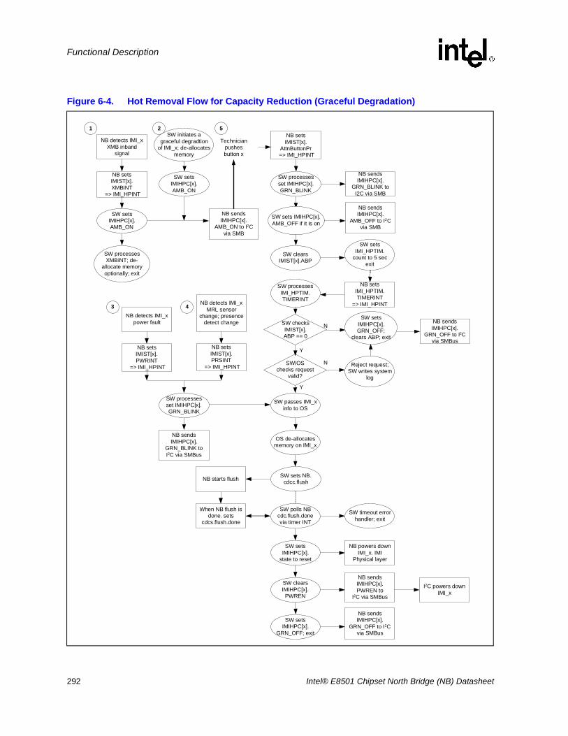
292 Intel® E8501 Chipset North Bridge (NB) Datasheet
Functional Description
Figure 6-4. Hot Removal Flow for Capacity Reduction (Graceful Degradation)
NB detects IMI_xXMB inband
signal
NB sendsIMIHPC[x].
GRN_BLINK toI2C via SMB
SW sets NB.cdcc.flush
SW setsIMIHPC[x].
state to reset
N Reject request;SW writes system
log
Y
SW processesset IMIHPC[x].GRN_BLINK
SW passes IMI_xinfo to OS
OS de-allocatesmemory on IMI_x
SW clearsIMIHPC[x].
PWREN
NB sendsIMIHPC[x].PWREN to
I2C via SMBus
NB powers downIMI_x. IMI
Physical layer
I2C powers downIMI_x
Technicianpushesbutton x
NB setsIMIST[x].
AttnButtonPr => IMI_HPINT
SW/OSchecks request
valid?
SW clearsIMIST[x].ABP
SW setsIMI_HPTIM.
count to 5 secexit
NB sendsIMIHPC[x].
GRN_OFF to I2Cvia SMBus
SW setsIMIHPC[x].
GRN_OFF; exit
NB setsIMIST[x].XMBINT
=> IMI_HPINT
NB sendsIMIHPC[x].
AMB_ON to I2Cvia SMB
SW setsIMIHPC[x].AMB_ON
N
Y
SW checksIMIST[x].ABP == 0
NB sendsIMIHPC[x].
GRN_OFF to I2Cvia SMBus
SW processesXMBINT; de-
allocate memoryoptionally; exit
NB starts flush
When NB flush isdone. sets
cdcs.flush.done
SW polls NBcdc.flush.donevia timer INT
SW setsIMIHPC[x].GRN_OFF;
clears ABP; exit
SW timeout errorhandler; exit
SW setsIMIHPC[x].AMB_ON
NB detects IMI_xpower fault
NB setsIMIST[x].PWRINT
=> IMI_HPINT
NB sendsIMIHPC[x].
AMB_OFF to I2Cvia SMB
SW processesset IMIHPC[x].GRN_BLINK
NB sendsIMIHPC[x].
GRN_BLINK toI2C via SMBus
NB detects IMI_xMRL sensor
change; presencedetect change
1 2
43
5SW initiates a
graceful degradtionof IMI_x; de-allocates
memory
SW processesIMI_HPTIM.TIMERINT
NB setsIMI_HPTIM.TIMERINT
=> IMI_HPINT
SW sets IMIHPC[x].AMB_OFF if it is on
NB setsIMIST[x].PRSINT
=> IMI_HPINT
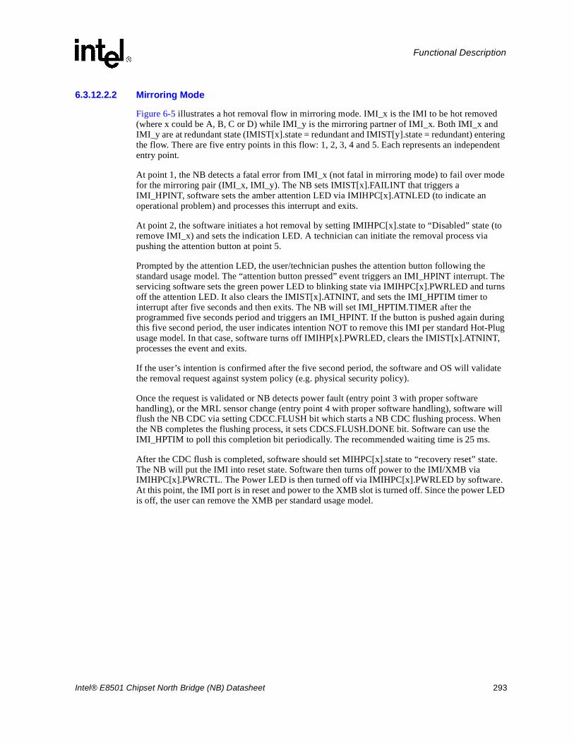
Intel® E8501 Chipset North Bridge (NB) Datasheet 293
Functional Description
6.3.12.2.2 Mirroring Mode
Figure 6-5 illustrates a hot removal flow in mirroring mode. IMI_x is the IMI to be hot removed (where x could be A, B, C or D) while IMI_y is the mirroring partner of IMI_x. Both IMI_x and IMI_y are at redundant state (IMIST[x].state = redundant and IMIST[y].state = redundant) entering the flow. There are five entry points in this flow: 1, 2, 3, 4 and 5. Each represents an independent entry point.
At point 1, the NB detects a fatal error from IMI_x (not fatal in mirroring mode) to fail over mode for the mirroring pair (IMI_x, IMI_y). The NB sets IMIST[x].FAILINT that triggers a IMI_HPINT, software sets the amber attention LED via IMIHPC[x].ATNLED (to indicate an operational problem) and processes this interrupt and exits.
At point 2, the software initiates a hot removal by setting IMIHPC[x].state to “Disabled” state (to remove IMI_x) and sets the indication LED. A technician can initiate the removal process via pushing the attention button at point 5.
Prompted by the attention LED, the user/technician pushes the attention button following the standard usage model. The “attention button pressed” event triggers an IMI_HPINT interrupt. The servicing software sets the green power LED to blinking state via IMIHPC[x].PWRLED and turns off the attention LED. It also clears the IMIST[x].ATNINT, and sets the IMI_HPTIM timer to interrupt after five seconds and then exits. The NB will set IMI_HPTIM.TIMER after the programmed five seconds period and triggers an IMI_HPINT. If the button is pushed again during this five second period, the user indicates intention NOT to remove this IMI per standard Hot-Plug usage model. In that case, software turns off IMIHP[x].PWRLED, clears the IMIST[x].ATNINT, processes the event and exits.
If the user’s intention is confirmed after the five second period, the software and OS will validate the removal request against system policy (e.g. physical security policy).
Once the request is validated or NB detects power fault (entry point 3 with proper software handling), or the MRL sensor change (entry point 4 with proper software handling), software will flush the NB CDC via setting CDCC.FLUSH bit which starts a NB CDC flushing process. When the NB completes the flushing process, it sets CDCS.FLUSH.DONE bit. Software can use the IMI_HPTIM to poll this completion bit periodically. The recommended waiting time is 25 ms.
After the CDC flush is completed, software should set MIHPC[x].state to “recovery reset” state. The NB will put the IMI into reset state. Software then turns off power to the IMI/XMB via IMIHPC[x].PWRCTL. The Power LED is then turned off via IMIHPC[x].PWRLED by software. At this point, the IMI port is in reset and power to the XMB slot is turned off. Since the power LED is off, the user can remove the XMB per standard usage model.
294 Intel® E8501 Chipset North Bridge (NB) Datasheet
Functional Description
Figure 6-5. Hot Removal for Mirroring Mode
NB detects IMI_xfatal failure
N Reject request;SW writes system
log
Y
Technicianpushesbutton x
I2C setsIMIST[x].
AttnButtonPr => IMI_HPINT
SWchecksrequestvalid?
NB sets partnerIMIST[y].state toRedundancyLos;
sets FAILINT=> IMI_HPINT
NB sendsIMIHPC[x].
AMB_ON to I2Cvia SMBus
SW setsIMIHPC[x].AMB_ON
N
Y
SW checksIMIST[x].ABP == 0
NB sendsIMIHPC[x].
GRN_OFF to I2Cvia SMBus
SW processesFAILINT
exit
SW setsIMIHPC[x].GRN_OFF;
clears ABP; exit
sets IMIST[x].state to
disabled;
NB sendsIMIHPC[x].
GRN_BLINK toI2C via SMBus
SW processesset IMIHPC[x].GRN_BLINK
SW clearsIMIST[x].ABP
SW setsIMI_HPTIM.
count to 5 secexit
NB setsIMI_HPTIM.TIMERINT
=> IMI_HPINT
SW processesIMI_HPTIM.TIMERINT
NB sendsIMIHPC[x].
AMB_OFF to I2Cvia SMBus
SW sets NB.cdcc.flush
NB sendsIMIHPC[x].PWREN to
I2C via SMBus
NB powers downIMI_x IMI
Physical layer
I2C powers downIMI_x
NB sendsIMIHPC[x].
GRN_OFF to I2Cvia SMBus
SW setsIMIHPC[x].
GRN_OFF; exit
NB starts flush
When NB flush isdone. sets
cdcs.flush.done
SW polls NBcdc.flush.donevia timer INT
SW timeout errorhandler; exit
SW setsIMIHPC[x].AMB_ON
exit
SW setsIMIHPC[x].
state to disabled
NB detects IMI_xpower fault
SW processesset IMIHPC[x].GRN_BLINK
NB sendsIMIHPC[x].
GRN_BLINK toI2C via SMBus
1 2
3 4 NB detects IMI_xMRL sensor
change; presencedetect change
SW setsIMIHPC[x].
AMB_OFF if it ison
5
NB sets partnerIMIST[y].state toRedundancyLos;
sets PWRINT=> IMI_HPINT
NB sets partnerIMIST[y].state toRedundancyLos;
sets PRSINT=> IMI_HPINT
NB RAID layerswitches txns to
IMI_y only;sets IMIST[x].
state to disabled;
NB RAID layerswitches txns to
IMI_y only;sets IMIST[x].
state to disabled;
N
Y
SWIMIST[x].state== disabled?
SW setsIMIHPC[x].
state to disabled
NB RAID layerswitches txnsto IMI_y only;sets IMIST[y].
RedundancyLoss
SW clearsIMIHPC[x].PWREN
SW sets IMIHPC[x].state to
recovery reset
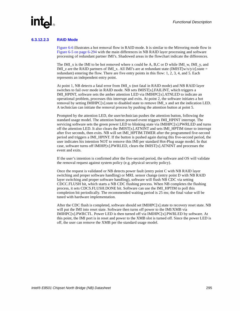
Intel® E8501 Chipset North Bridge (NB) Datasheet 295
Functional Description
6.3.12.2.3 RAID Mode
Figure 6-6 illustrates a hot removal flow in RAID mode. It is similar to the Mirroring mode flow in Figure 6-5 on page 6-294 with the main differences in NB RAID layer processing and software processing of redundant partner IMI’s. Shadowed areas in the flowchart indicate the differences.
The IMI_x is the IMI to be hot removed where x could be A, B,C or D while IMI_w, IMI_y, and IMI_z are the RAID partners of IMI_x. All IMI’s are at redundant state (IMIST[w/x/y/z].state = redundant) entering the flow. There are five entry points in this flow: 1, 2, 3, 4, and 5. Each represents an independent entry point.
At point 1, NB detects a fatal error from IMI_x (not fatal in RAID mode) and NB RAID layer switches to fail over mode in RAID mode. NB sets IMIST[x].FAILINT, which triggers a IMI_HPINT, software sets the amber attention LED via IMIHPC[x].ATNLED to indicate an operational problem, processes this interrupt and exits. At point 2, the software initiates a hot removal by setting IMIHPC[x].state to disabled state to remove IMI_x and set the indication LED. A technician can initiate the removal process by pushing the attention button at point 5.
Prompted by the attention LED, the user/technician pushes the attention button, following the standard usage model. The attention button pressed event triggers IMI_HPINT interrupt. The servicing software sets the green power LED to blinking state via IMIHPC[x].PWRLED and turns off the attention LED. It also clears the IMIST[x].ATNINT and sets IMI_HPTIM timer to interrupt after five seconds, then exits. NB will set IMI_HPTIM.TIMER after the programmed five-second period and triggers a IMI_HPINT. If the button is pushed again during this five-second period, the user indicates his intention NOT to remove this IMI per standard Hot-Plug usage model. In that case, software turns off IMIHP[x].PWRLED, clears the IMIST[x].ATNINT and processes the event and exits.
If the user’s intention is confirmed after the five-second period, the software and OS will validate the removal request against system policy (e.g. physical security policy).
Once the request is validated or NB detects power fault (entry point C with NB RAID layer switching and proper software handling) or MRL sensor change (entry point D with NB RAID layer switching and proper software handling), software will flush NB CDC via setting CDCC.FLUSH bit, which starts a NB CDC flushing process. When NB completes the flushing process, it sets CDCS.FLUSH.DONE bit. Software can use the IMI_HPTIM to poll this completion bit periodically. The recommended waiting period is 25 ms; the final value will be tuned with hardware implementation.
After the CDC flush is completed, software should set IMIHPC[x].state to recovery reset state. NB will put the IMI into reset state. Software then turns off power to the IMI/XMB via IMIHPC[x].PWRCTL. Power LED is then turned off via IMIHPC[x].PWRLED by software. At this point, the IMI port is in reset and power to the XMB slot is turned off. Since the power LED is off, the user can remove the XMB per the standard usage model.
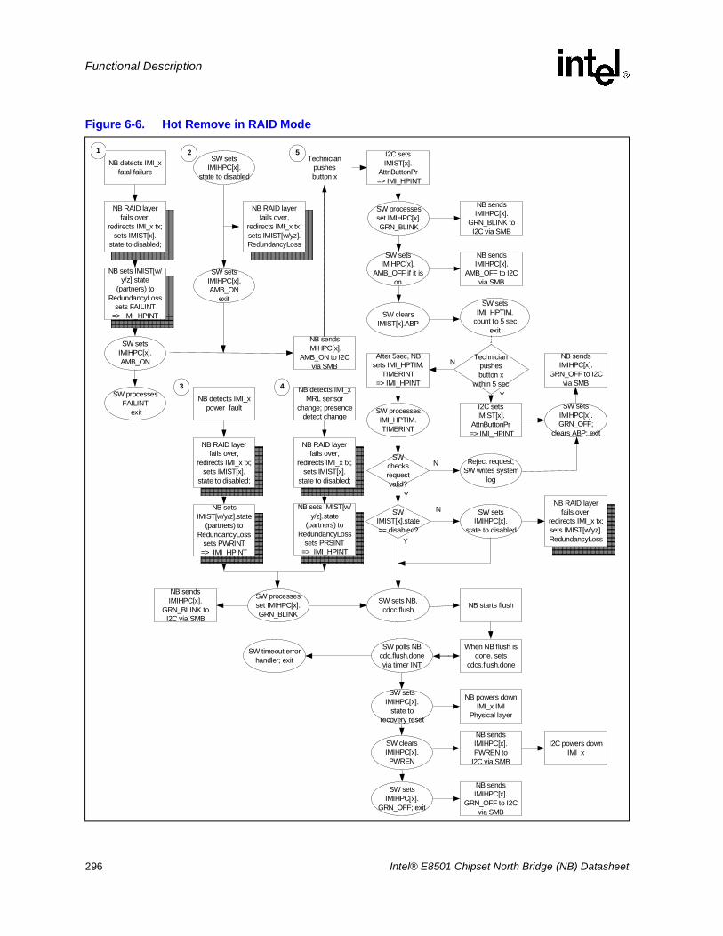
296 Intel® E8501 Chipset North Bridge (NB) Datasheet
Functional Description
Figure 6-6. Hot Remove in RAID Mode
NB detects IMI_xfatal failure
Technicianpushesbutton x
I2C setsIMIST[x].
AttnButtonPr => IMI_HPINT
NB sendsIMIHPC[x].
AMB_ON to I2Cvia SMB
SW setsIMIHPC[x].AMB_ON
SW processesFAILINT
exit
NB sendsIMIHPC[x].
GRN_BLINK toI2C via SMB
SW processesset IMIHPC[x].GRN_BLINK
SW clearsIMIST[x].ABP
SW setsIMI_HPTIM.
count to 5 secexit
NB sendsIMIHPC[x].
AMB_OFF to I2Cvia SMB
SW sets NB.cdcc.flush
NB sendsIMIHPC[x].PWREN to
I2C via SMB
NB powers downIMI_x IMI
Physical layer
I2C powers downIMI_x
NB sendsIMIHPC[x].
GRN_OFF to I2Cvia SMB
SW setsIMIHPC[x].
GRN_OFF; exit
NB starts flush
When NB flush isdone. sets
cdcs.flush.done
SW polls NBcdc.flush.donevia timer INT
SW timeout errorhandler; exit
SW setsIMIHPC[x].AMB_ON
exit
SW setsIMIHPC[x].
state to disabled
NB detects IMI_xpower fault
SW processesset IMIHPC[x].GRN_BLINK
NB sendsIMIHPC[x].
GRN_BLINK toI2C via SMB
1 2
3 4 NB detects IMI_xMRL sensor
change; presencedetect change
SW setsIMIHPC[x].
AMB_OFF if it ison
NB RAID layerfails over,
redirects IMI_x tx;sets IMIST[x].
state to disabled;
NB RAID layerfails over,
redirects IMI_x tx;sets IMIST[w/yz].RedundancyLoss
NB sets IMIST[w/y/z].state
(partners) toRedundancyLoss
sets FAILINT=> IMI_HPINT
NB RAID layerfails over,
redirects IMI_x tx;sets IMIST[x].
state to disabled;
NB setsIMIST[w/y/z].state
(partners) toRedundancyLoss
sets PWRINT=> IMI_HPINT
NB sets IMIST[w/y/z].state
(partners) toRedundancyLoss
sets PRSINT=> IMI_HPINT
NB RAID layerfails over,
redirects IMI_x tx;sets IMIST[x].
state to disabled;
N
Y
SWIMIST[x].state== disabled?
SW setsIMIHPC[x].
state to disabled
5
Y
N Reject request;SW writes system
log
SWchecksrequestvalid?
NB sendsIMIHPC[x].
GRN_OFF to I2Cvia SMB
SW setsIMIHPC[x].GRN_OFF;
clears ABP; exit
After 5sec, NBsets IMI_HPTIM.
TIMERINT=> IMI_HPINT
SW processesIMI_HPTIM.TIMERINT
Technicianpushesbutton x
within 5 sec
N
YI2C setsIMIST[x].
AttnButtonPr => IMI_HPINT
NB RAID layerfails over,
redirects IMI_x tx;sets IMIST[w/yz].RedundancyLoss
SW setsIMIHPC[x].
state torecovery reset
SW clearsIMIHPC[x].PWREN
Intel® E8501 Chipset North Bridge (NB) Datasheet 297
Functional Description
6.3.13 Memory Hot AdditionSoftware/User initiates hot addition for preventative maintenance or add-on upgrade purposes. NB could support at least two approaches:
• The user inserts an XMB card, closes the MRL switch and then pushes the attention button on a XMB card to indicate hot addition intention.
• User requests hot addition through system software user interface.
Hot addition flows in the chapter illustrate the attention button mechanism only.
6.3.13.1 Normal Mode
Figure 6-7 illustrates a hot addition flow in normal mode. The IMI_x is the IMI to be hot added (where x could be A,B, C or D). IMI_x is at reset state (IMIST[x].state = reset) entering the flow.
At point A, the user/technician inserts a XMB card into slot x and closes the MRL switch. The NB sets IMIST[x].PRSINT, and triggers an IMI_HPINT interrupt. Servicing software processes this interrupt and records the possible addition of IMI_x. The user then pushes the attention button following the standard usage model. The “attention button pressed” event triggers the IMI_HPINT interrupt. The servicing software sets the green power LED to “blinking state” via IMIHPC[x].PWRLED. It also clears the IMIST[x].ATNINT and sets IMI_HPTIM timer to interrupt after five seconds and then exits. The NB will set IMI_HPTIM.TIMER after the programmed five second period and triggers an IMI_HPINT. If the button is pushed again during this five second period, the user indicates intention NOT to add this IMI per standard Hot-Plug usage model. In that case, software turns off the IMIHP[x].PWRLED, clears the IMIST[x].ATNINT, processes the event and exits.
If the user’s intention is confirmed after the five second period, the software and OS will validate the addition request against system policy (e.g. physical security policy).
Once the request is validated, software sets the IMI state to reset for a clean start. Software then advances the IMI state to initialization, and the NB will start the initialization process. When the NB completes the initialization process, it sets the IMIST[x].STATE to “ready” state. Software can use the IMI_HPTIM to poll this completion bit periodically. The recommended waiting time is 25 ms.
Once the IMI is in “ready” state, software performs memory configuration, memory testing and memory calibration. If the XMB memory passes the testing and calibration, then software sets the IMIHPC[x].STATE to active and programs IMIR’s. The OS will allocate the system memory in this IMI/XMB. This hot addition is completed successfully.
If the XMB memory does not pass the testing and calibration, software sets the IMI state back to reset and turns on the amber attention LED to report operational problem. Software then turns off the XMB slot power via IMIHPC[x].PWREN and turns off green power LED. Finally, software writes to the system log and exits.
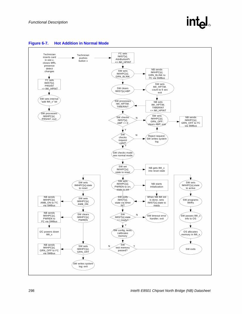
298 Intel® E8501 Chipset North Bridge (NB) Datasheet
Functional Description
Figure 6-7. Hot Addition in Normal Mode
NB sendsIMIHPC[x].
GRN_BLINK toI2C via SMBus
SW setIMIHPC[x].
state to reset
Y
SW setsIMIHPC[x].
GRN_BLINK
SW setsIMIHPC[x].state
to active
NB gets IMI_xinto reset state
Technicianpushesbutton x
I2C setsIMIST[x].
AttnButtonPr => IMI_HPINT
SW sets internal“add IMI_x” bit
SW processesIMIHPC[x].
PRSINT; exit
SW setsIMIHPC[x].
PWREN to on;state to init
I2C setsIMIST[x].PRSINT
=> IMI_HPINT
Technicianinserts card
in slot x;closes MRL
presencedetect
changes
NB startsinitialization
SWIMIST[x].state
== ready?
SW passes IMI_xinfo to OS
OS allocatesmemory in IMI_x
N
Y
SW programsIMIRs
SW config, tests.calibratesmemory
SWtest memory
passed?
YN
SW setsIMIHPC[x].state
to reset
N Reject request;SW writes system
log
SWchecksrequestvalid?
N
Y
SW checksIMIST[x].ABP == 0
NB sendsIMIHPC[x].
GRN_OFF to I2Cvia SMBus
SW setsIMIHPC[x].GRN_OFF;
clears ABP; exit
SW clearsIMIST[x].ABP
SW setsIMI_HPTIM.
count to 5 secexit
NB setsIMI_HPTIM.TIMERINT
=> IMI_HPINT
SW processesIMI_HPTIM.TIMERINT
When NB IMI initis done, sets
IMIST[x].state toready
SW pollsIMIST[x].
state via timerINT
SW timeout errorhandler; exit
SW setsIMIHPC[x].AMB_ON
NB sendsIMIHPC[x].
AMB_ON to I2Cvia SMBus
NB sendsIMIHPC[x].
GRN_OFF to I2Cvia SMBus
SW setsIMIHPC[x].GRN_OFF
SW writes systemlog; exit
SW exits
SW checks modesee normal mode
SW clearsIMIHPC[x].
PWREN
NB sendsIMIHPC[x].PWREN to
I2C via SMBus
I2C powers downIMI_x
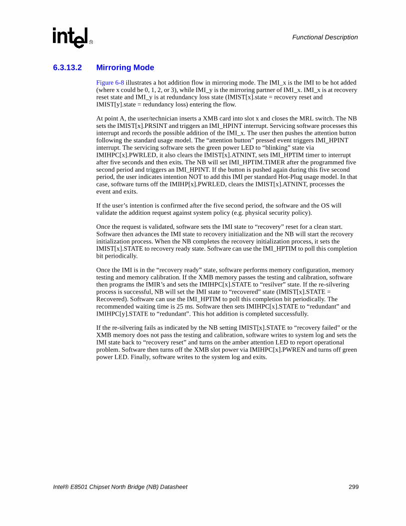
Intel® E8501 Chipset North Bridge (NB) Datasheet 299
Functional Description
6.3.13.2 Mirroring Mode
Figure 6-8 illustrates a hot addition flow in mirroring mode. The IMI_x is the IMI to be hot added (where x could be 0, 1, 2, or 3), while IMI_y is the mirroring partner of IMI_x. IMI_x is at recovery reset state and IMI_y is at redundancy loss state (IMIST[x].state = recovery reset and IMIST[y].state = redundancy loss) entering the flow.
At point A, the user/technician inserts a XMB card into slot x and closes the MRL switch. The NB sets the IMIST[x].PRSINT and triggers an IMI_HPINT interrupt. Servicing software processes this interrupt and records the possible addition of the IMI_x. The user then pushes the attention button following the standard usage model. The “attention button” pressed event triggers IMI_HPINT interrupt. The servicing software sets the green power LED to “blinking” state via IMIHPC[x].PWRLED, it also clears the IMIST[x].ATNINT, sets IMI_HPTIM timer to interrupt after five seconds and then exits. The NB will set IMI_HPTIM.TIMER after the programmed five second period and triggers an IMI_HPINT. If the button is pushed again during this five second period, the user indicates intention NOT to add this IMI per standard Hot-Plug usage model. In that case, software turns off the IMIHP[x].PWRLED, clears the IMIST[x].ATNINT, processes the event and exits.
If the user’s intention is confirmed after the five second period, the software and the OS will validate the addition request against system policy (e.g. physical security policy).
Once the request is validated, software sets the IMI state to “recovery” reset for a clean start. Software then advances the IMI state to recovery initialization and the NB will start the recovery initialization process. When the NB completes the recovery initialization process, it sets the IMIST[x].STATE to recovery ready state. Software can use the IMI_HPTIM to poll this completion bit periodically.
Once the IMI is in the “recovery ready” state, software performs memory configuration, memory testing and memory calibration. If the XMB memory passes the testing and calibration, software then programs the IMIR’s and sets the IMIHPC[x].STATE to “resilver” state. If the re-silvering process is successful, NB will set the IMI state to “recovered” state (IMIST[x].STATE = Recovered). Software can use the IMI_HPTIM to poll this completion bit periodically. The recommended waiting time is 25 ms. Software then sets IMIHPC[x].STATE to “redundant” and IMIHPC[y].STATE to “redundant”. This hot addition is completed successfully.
If the re-silvering fails as indicated by the NB setting IMIST[x].STATE to “recovery failed” or the XMB memory does not pass the testing and calibration, software writes to system log and sets the IMI state back to “recovery reset” and turns on the amber attention LED to report operational problem. Software then turns off the XMB slot power via IMIHPC[x].PWREN and turns off green power LED. Finally, software writes to the system log and exits.
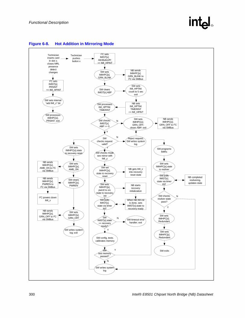
300 Intel® E8501 Chipset North Bridge (NB) Datasheet
Functional Description
Figure 6-8. Hot Addition in Mirroring Mode
NB sendsIMIHPC[x].
GRN_BLINK toI2C via SMBus
SW setsIMIHPC[x].
GRN_BLINK
Technicianpushesbutton x
I2C setsIMIST[x].
AttnButtonPr => IMI_HPINT
SW setsIMIHPC[x].Redundant
SW checks modesee mirror with
IMI_y
SW setsIMIHPC[y].Redundant
NB completedresilvering,
updates state
SW checksresilver state
pass?
Y
N
Y
N
N
Y
NB sendsIMIHPC[x].
GRN_OFF to I2Cvia SMBus
SW setsIMIHPC[x].GRN_OFF;
clears ABP; exit
SW clearsIMIST[x].ABP
NB setsIMI_HPTIM.TIMERINT
=> IMI_HPINT
SW processesIMI_HPTIM.TIMERINT
NB gets IMI_xinto recoveryreset state
NB startsrecovery
initialization
SWIMIST[x].state== recovery
ready?
N
Y
SWtest memory
passed?
Y
N
SW setsIMIHPC[x].stateto recovery reset
When NB IMI initis done, sets
IMIST[x].state torecovery ready
SW pollsIMIST[x].
state via timerINT
SW timeout errorhandler; exit
SW setsIMIHPC[x].AMB_ON
NB sendsIMIHPC[x].
AMB_ON to I2Cvia SMBus
NB sendsIMIHPC[x].
GRN_OFF to I2Cvia SMBus
SW setsIMIHPC[x].GRN_OFF
SW writes systemlog; exit
SW clearsIMIHPC[x].PWREN
NB sendsIMIHPC[x].PWREN to
I2C via SMBus
I2C powers downIMI_x
SW setsIMIHPC[x].state
to resilver
SW programsIMIRs
SW exits
SW writes systemlog
SW sets internal“add IMI_x” bit
SW processesIMIHPC[x].
PRSINT; exit
I2C setsIMIST[x].PRSINT
=> IMI_HPINT
Technicianinserts card
in slot x;closes MRLpresence
detectchanges
SW pollsIMIST[x].
state via timerINT
SW config, tests.calibrates memory
SW setIMIHPC[x].
state to recoveryreset
SW checksIMIST[x].ABP == 0
SWchecks request
valid?
Reject request;SW writes system
log
SW setsIMI_HPTIM.
count to 5 secexit
SW setsIMIHPC[x].pwrctl to on;
state to recovery init
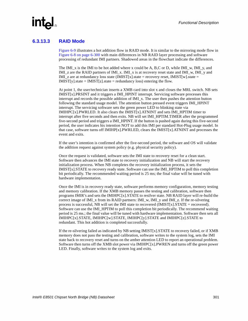
Intel® E8501 Chipset North Bridge (NB) Datasheet 301
Functional Description
6.3.13.3 RAID Mode
Figure 6-9 illustrates a hot addition flow in RAID mode. It is similar to the mirroring mode flow in Figure 6-8 on page 6-300 with main differences in NB RAID layer processing and software processing of redundant IMI partners. Shadowed areas in the flowchart indicate the differences.
The IMI_x is the IMI to be hot added where x could be A, B,C or D, while IMI_w, IMI_y, and IMI_z are the RAID partners of IMI_x. IMI_x is at recovery reset state and IMI_w, IMI_y and IMI_z are at redundancy loss state (IMIST[x].state = recovery reset, IMIST[w].state = IMIST[y].state = IMIST[z].state = redundancy loss) entering the flow.
At point 1, the user/technician inserts a XMB card into slot x and closes the MRL switch. NB sets IMIST[x].PRSINT and it triggers a IMI_HPINT interrupt. Servicing software processes this interrupt and records the possible addition of IMI_x. The user then pushes the attention button following the standard usage model. The attention button pressed event triggers IMI_HPINT interrupt. The servicing software sets the green power LED to blinking state via IMIHPC[x].PWRLED. It also clears the IMIST[x].ATNINT and sets IMI_HPTIM timer to interrupt after five seconds and then exits. NB will set IMI_HPTIM.TIMER after the programmed five-second period and triggers a IMI_HPINT. If the button is pushed again during this five-second period, the user indicates his intention NOT to add this IMI per standard Hot-Plug usage model. In that case, software turns off IMIHP[x].PWRLED, clears the IMIST[x].ATNINT and processes the event and exits.
If the user’s intention is confirmed after the five-second period, the software and OS will validate the addition request against system policy (e.g. physical security policy).
Once the request is validated, software sets the IMI state to recovery reset for a clean start. Software then advances the IMI state to recovery initialization and NB will start the recovery initialization process. When NB completes the recovery initialization process, it sets the IMIST[x].STATE to recovery ready state. Software can use the IMI_HPTIM to poll this completion bit periodically. The recommended waiting period is 25 ms; the final value will be tuned with hardware implementation.
Once the IMI is in recovery ready state, software performs memory configuration, memory testing and memory calibration. If the XMB memory passes the testing and calibration, software then programs IMIR’s and sets the IMIHPC[x].STATE to resilver state. NB RAID layer will re-build the correct image of IMI_x from its RAID partners: IMI_w, IMI_y and IMI_z. If the re-silvering process is successful, NB will set the IMI state to recovered (IMIST[x].STATE = recovered). Software can use the IMI_HPTIM to poll this completion bit periodically. The recommend waiting period is 25 ms.; the final value will be tuned with hardware implementation. Software then sets all IMIHPC[x].STATE, IMIHPC[w].STATE, IMIHPC[y].STATE and IMIHPC[z].STATE to redundant. This hot addition is completed successfully.
If the re-silvering failed as indicated by NB setting IMIST[x].STATE to recovery failed, or if XMB memory does not pass the testing and calibration, software writes to the system log, sets the IMI state back to recovery reset and turns on the amber attention LED to report an operational problem. Software then turns off the XMB slot power via IMIHPC[x].PWREN and turns off the green power LED. Finally, software writes to the system log and exits.
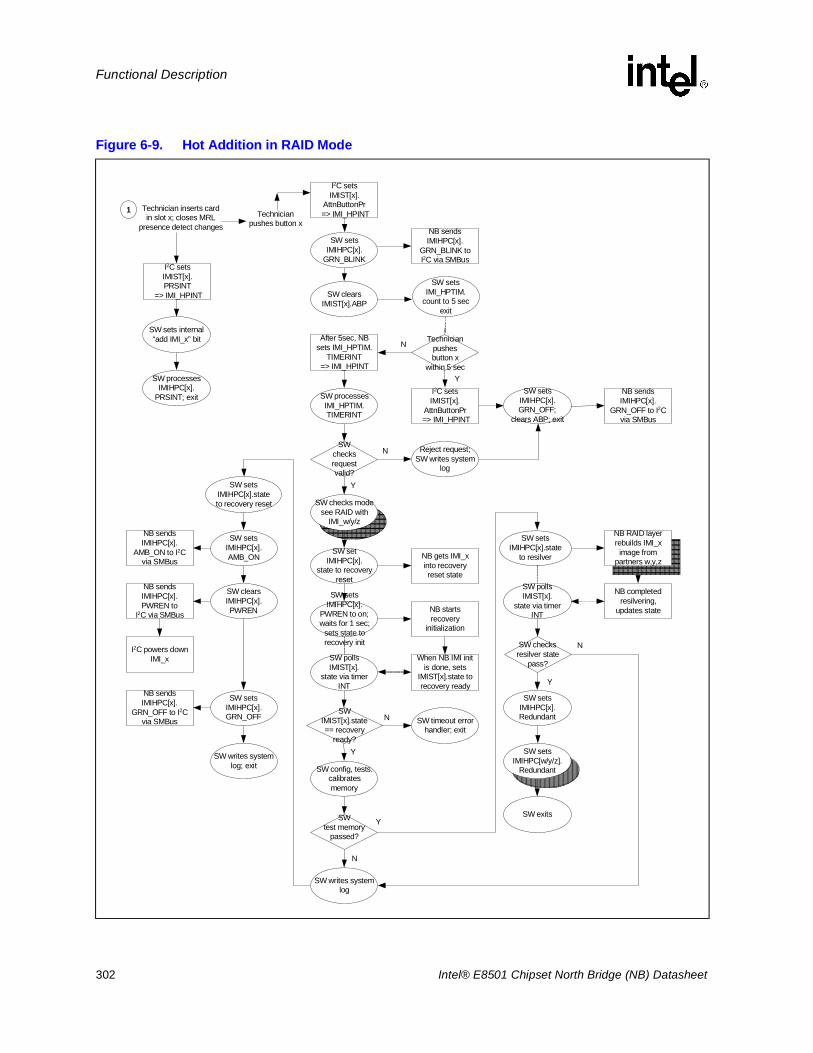
302 Intel® E8501 Chipset North Bridge (NB) Datasheet
Functional Description
Figure 6-9. Hot Addition in RAID Mode
SW checks modesee RAID with
IMI_w/y/z
NB sendsIMIHPC[x].
GRN_BLINK toI2C via SMBus
Technicianpushes button x
I2C setsIMIST[x].
AttnButtonPr => IMI_HPINT
SW setsIMIHPC[x].Redundant
SW setsIMIHPC[w/y/z].
Redundant
NB RAID layerrebuilds IMI_x
image frompartners w,y,z
NB completedresilvering,
updates state
SW checksresilver state
pass?
Y
N
Y
N Reject request;SW writes system
log
SWchecksrequestvalid?
NB sendsIMIHPC[x].
GRN_OFF to I2Cvia SMBus
SW setsIMIHPC[x].GRN_OFF;
clears ABP; exit
SW clearsIMIST[x].ABP
SW setsIMI_HPTIM.
count to 5 secexit
After 5sec, NBsets IMI_HPTIM.
TIMERINT=> IMI_HPINT
SW processesIMI_HPTIM.TIMERINT
SW setIMIHPC[x].
state to recoveryreset
NB gets IMI_xinto recoveryreset state
SW setsIMIHPC[x].
PWREN to on;waits for 1 sec;
sets state torecovery init
NB startsrecovery
initialization
SWIMIST[x].state== recovery
ready?
N
Y
SW config, tests.calibratesmemory
SWtest memory
passed?
Y
N
SW setsIMIHPC[x].stateto recovery reset
When NB IMI initis done, sets
IMIST[x].state torecovery ready
SW pollsIMIST[x].
state via timerINT
SW timeout errorhandler; exit
SW setsIMIHPC[x].AMB_ON
NB sendsIMIHPC[x].
AMB_ON to I2Cvia SMBus
NB sendsIMIHPC[x].
GRN_OFF to I2Cvia SMBus
SW setsIMIHPC[x].GRN_OFF
SW writes systemlog; exit
SW clearsIMIHPC[x].PWREN
NB sendsIMIHPC[x].PWREN to
I2C via SMBus
I2C powers downIMI_x
SW setsIMIHPC[x].state
to resilver
SW exits
SW pollsIMIST[x].
state via timerINT
SW writes systemlog
1
SW sets internal“add IMI_x” bit
SW processesIMIHPC[x].
PRSINT; exit
I2C setsIMIST[x].PRSINT
=> IMI_HPINT
Technician inserts cardin slot x; closes MRL
presence detect changes
Technicianpushesbutton x
within 5 sec
N
YI2C setsIMIST[x].
AttnButtonPr => IMI_HPINT
SW setsIMIHPC[x].
GRN_BLINK
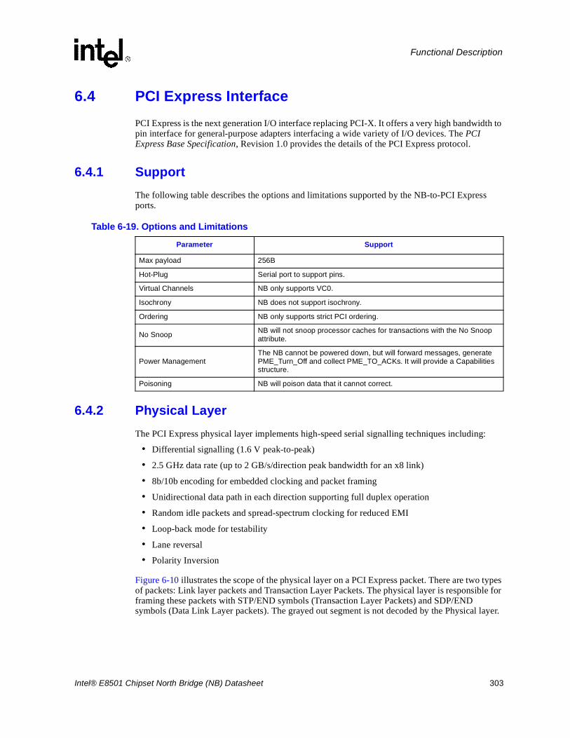
Intel® E8501 Chipset North Bridge (NB) Datasheet 303
Functional Description
6.4 PCI Express InterfacePCI Express is the next generation I/O interface replacing PCI-X. It offers a very high bandwidth to pin interface for general-purpose adapters interfacing a wide variety of I/O devices. The PCI Express Base Specification, Revision 1.0 provides the details of the PCI Express protocol.
6.4.1 SupportThe following table describes the options and limitations supported by the NB-to-PCI Express ports.
6.4.2 Physical LayerThe PCI Express physical layer implements high-speed serial signalling techniques including:
• Differential signalling (1.6 V peak-to-peak)
• 2.5 GHz data rate (up to 2 GB/s/direction peak bandwidth for an x8 link)
• 8b/10b encoding for embedded clocking and packet framing
• Unidirectional data path in each direction supporting full duplex operation
• Random idle packets and spread-spectrum clocking for reduced EMI
• Loop-back mode for testability
• Lane reversal
• Polarity Inversion
Figure 6-10 illustrates the scope of the physical layer on a PCI Express packet. There are two types of packets: Link layer packets and Transaction Layer Packets. The physical layer is responsible for framing these packets with STP/END symbols (Transaction Layer Packets) and SDP/END symbols (Data Link Layer packets). The grayed out segment is not decoded by the Physical layer.
Table 6-19. Options and Limitations
Parameter Support
Max payload 256B
Hot-Plug Serial port to support pins.
Virtual Channels NB only supports VC0.
Isochrony NB does not support isochrony.
Ordering NB only supports strict PCI ordering.
No Snoop NB will not snoop processor caches for transactions with the No Snoop attribute.
Power ManagementThe NB cannot be powered down, but will forward messages, generate PME_Turn_Off and collect PME_TO_ACKs. It will provide a Capabilities structure.
Poisoning NB will poison data that it cannot correct.
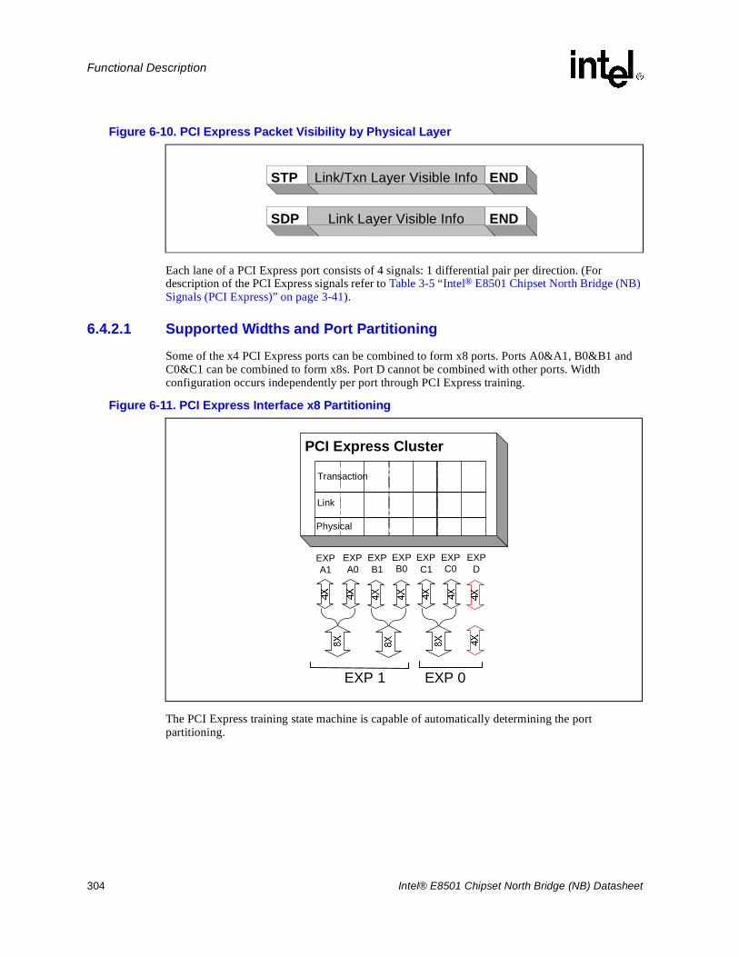
304 Intel® E8501 Chipset North Bridge (NB) Datasheet
Functional Description
Each lane of a PCI Express port consists of 4 signals: 1 differential pair per direction. (For description of the PCI Express signals refer to Table 3-5 “Intel® E8501 Chipset North Bridge (NB) Signals (PCI Express)” on page 3-41).
6.4.2.1 Supported Widths and Port Partitioning
Some of the x4 PCI Express ports can be combined to form x8 ports. Ports A0&A1, B0&B1 and C0&C1 can be combined to form x8s. Port D cannot be combined with other ports. Width configuration occurs independently per port through PCI Express training.
The PCI Express training state machine is capable of automatically determining the port partitioning.
Figure 6-10. PCI Express Packet Visibility by Physical Layer
STP Link/Txn Layer Visible Info END
SDP Link Layer Visible Info END
Figure 6-11. PCI Express Interface x8 Partitioning
PCI Express Cluster
Transaction
Link
Physical
EXPA1
EXPA0
EXPB1
EXPB0
EXPC1
EXPC0
EXPD
EXP 1 EXP 0
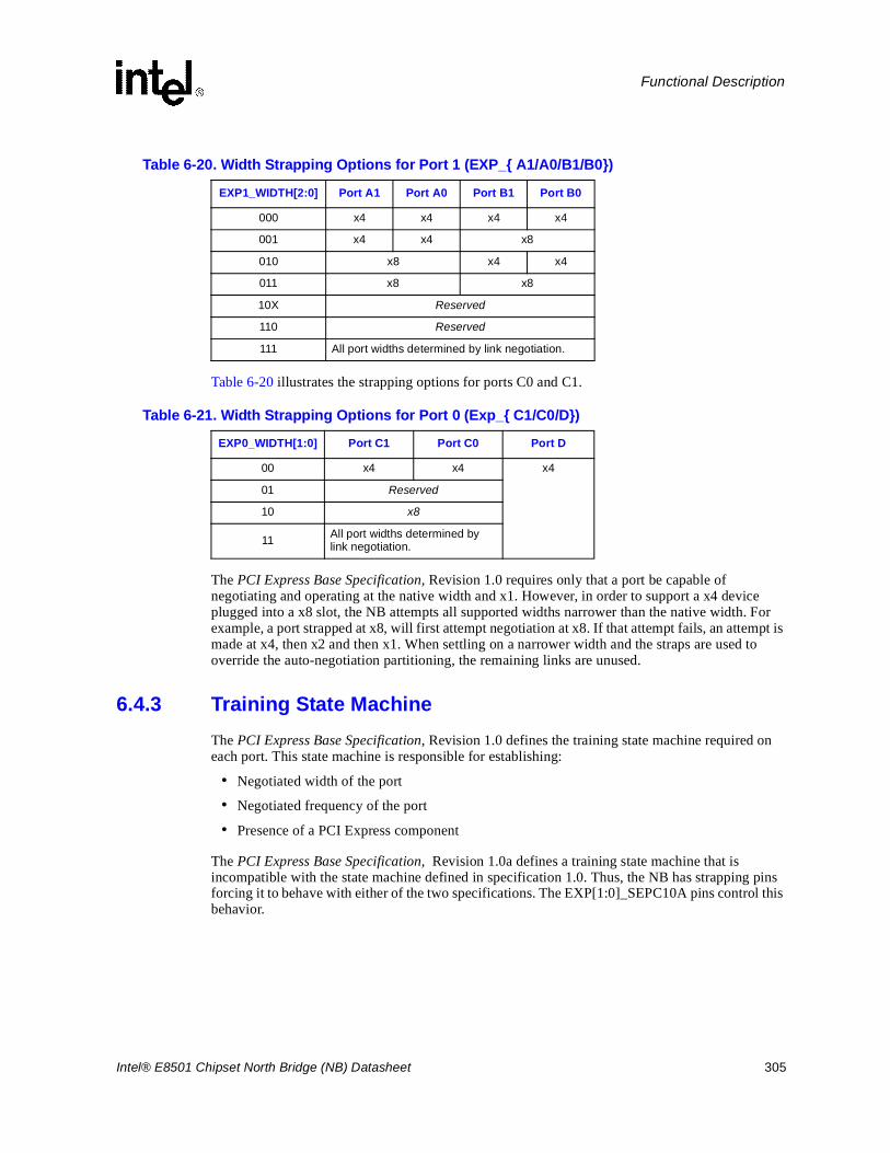
Intel® E8501 Chipset North Bridge (NB) Datasheet 305
Functional Description
Table 6-20 illustrates the strapping options for ports C0 and C1.
The PCI Express Base Specification, Revision 1.0 requires only that a port be capable of negotiating and operating at the native width and x1. However, in order to support a x4 device plugged into a x8 slot, the NB attempts all supported widths narrower than the native width. For example, a port strapped at x8, will first attempt negotiation at x8. If that attempt fails, an attempt is made at x4, then x2 and then x1. When settling on a narrower width and the straps are used to override the auto-negotiation partitioning, the remaining links are unused.
6.4.3 Training State MachineThe PCI Express Base Specification, Revision 1.0 defines the training state machine required on each port. This state machine is responsible for establishing:
• Negotiated width of the port
• Negotiated frequency of the port
• Presence of a PCI Express component
The PCI Express Base Specification, Revision 1.0a defines a training state machine that is incompatible with the state machine defined in specification 1.0. Thus, the NB has strapping pins forcing it to behave with either of the two specifications. The EXP[1:0]_SEPC10A pins control this behavior.
Table 6-20. Width Strapping Options for Port 1 (EXP_{ A1/A0/B1/B0})
EXP1_WIDTH[2:0] Port A1 Port A0 Port B1 Port B0
000 x4 x4 x4 x4
001 x4 x4 x8
010 x8 x4 x4
011 x8 x8
10X Reserved
110 Reserved
111 All port widths determined by link negotiation.
Table 6-21. Width Strapping Options for Port 0 (Exp_{ C1/C0/D})
EXP0_WIDTH[1:0] Port C1 Port C0 Port D
00 x4 x4 x4
01 Reserved
10 x8
11 All port widths determined by link negotiation.
306 Intel® E8501 Chipset North Bridge (NB) Datasheet
Functional Description
6.4.4 Link LayerThe Data Link Layer of the PCI Express protocol is primarily responsible for data integrity. This is accomplished with the following elements:
• Sequence number assignment for each packet
• ACK/NAK protocol to ensure successful transmission of every packet
• CRC protection of packets
• Time-out mechanism to detect “lost” packets
• Credit exchange
Figure 6-12 illustrates the scope of the link layer on a PCI Express packet. There are two types of packets: Data Link Layer Packets (DLLP) and Transaction Layer Packets (TLP). Data Link Layer Packets are sent between the Link Layers of each PCI Express device and do not proceed to the Transaction Layer.
For Transaction Layer Packets (TLP), the Link Layer is responsible for prepending sequence numbers and appending 32-bit CRC. The grayed out segment is not decoded by the Data Link Layer.
6.4.4.1 Data Link Layer Packets (DLLP)
Refer to PCI Express Base Specification, Revision 1.0 for an explicit definition of all the fields in a Data Link Layer packet.
DLLP’s are used to ACK or NAK packets as they are sent from the transmitter to the receiver. They are sent by the receivers of the packet to indicate to the transmitter that a packet was successfully received (ACK) or not (NAK). DLLP’s are also used to exchange credit information between the transmitter and receiver.
Table 6-22. Training State Machine Mode
Pin Value Function
EXP0_SEPC10A0 PCI Express ports D, C0, C1 will use 1.0 specification.
1 PCI Express ports D, C0, C1 will use 1.0a specification.
EXP1_SPEC10A0 PCI Express ports B0, B1, A0, A1 will use 1.0 specification.
1 PCI Express ports B0, B1, A0, A1 will use 1.0a specification.
Figure 6-12. PCI Express Packet Visibility by Link Layer
Seq # TLP CRC
DLLP
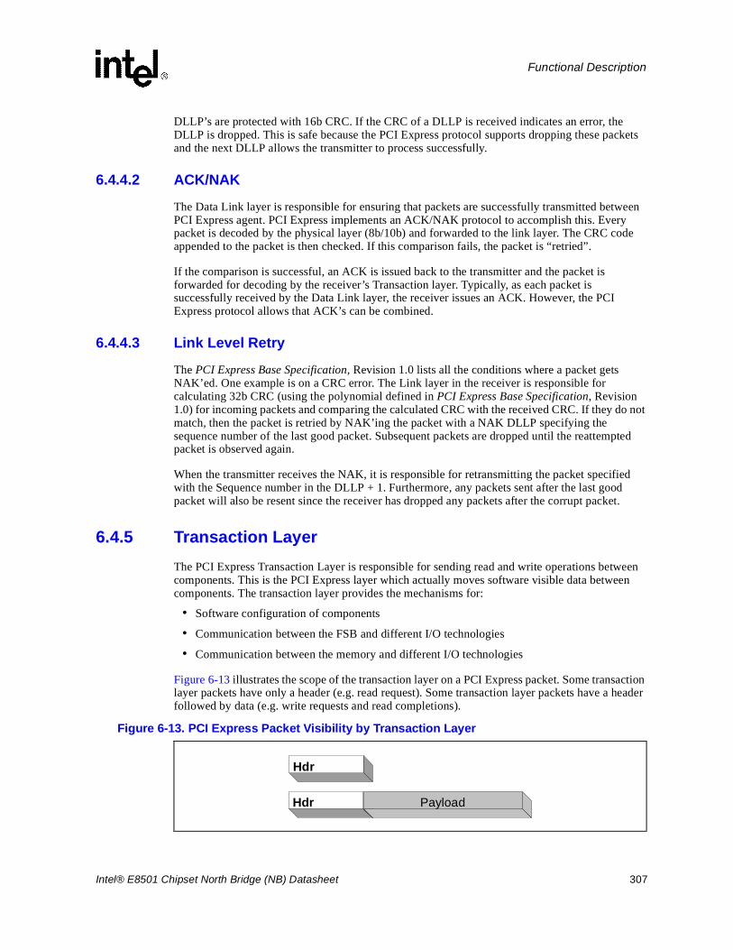
Intel® E8501 Chipset North Bridge (NB) Datasheet 307
Functional Description
DLLP’s are protected with 16b CRC. If the CRC of a DLLP is received indicates an error, the DLLP is dropped. This is safe because the PCI Express protocol supports dropping these packets and the next DLLP allows the transmitter to process successfully.
6.4.4.2 ACK/NAK
The Data Link layer is responsible for ensuring that packets are successfully transmitted between PCI Express agent. PCI Express implements an ACK/NAK protocol to accomplish this. Every packet is decoded by the physical layer (8b/10b) and forwarded to the link layer. The CRC code appended to the packet is then checked. If this comparison fails, the packet is “retried”.
If the comparison is successful, an ACK is issued back to the transmitter and the packet is forwarded for decoding by the receiver’s Transaction layer. Typically, as each packet is successfully received by the Data Link layer, the receiver issues an ACK. However, the PCI Express protocol allows that ACK’s can be combined.
6.4.4.3 Link Level Retry
The PCI Express Base Specification, Revision 1.0 lists all the conditions where a packet gets NAK’ed. One example is on a CRC error. The Link layer in the receiver is responsible for calculating 32b CRC (using the polynomial defined in PCI Express Base Specification, Revision 1.0) for incoming packets and comparing the calculated CRC with the received CRC. If they do not match, then the packet is retried by NAK’ing the packet with a NAK DLLP specifying the sequence number of the last good packet. Subsequent packets are dropped until the reattempted packet is observed again.
When the transmitter receives the NAK, it is responsible for retransmitting the packet specified with the Sequence number in the DLLP + 1. Furthermore, any packets sent after the last good packet will also be resent since the receiver has dropped any packets after the corrupt packet.
6.4.5 Transaction LayerThe PCI Express Transaction Layer is responsible for sending read and write operations between components. This is the PCI Express layer which actually moves software visible data between components. The transaction layer provides the mechanisms for:
• Software configuration of components
• Communication between the FSB and different I/O technologies
• Communication between the memory and different I/O technologies
Figure 6-13 illustrates the scope of the transaction layer on a PCI Express packet. Some transaction layer packets have only a header (e.g. read request). Some transaction layer packets have a header followed by data (e.g. write requests and read completions).
Figure 6-13. PCI Express Packet Visibility by Transaction Layer
Hdr
Hdr Payload
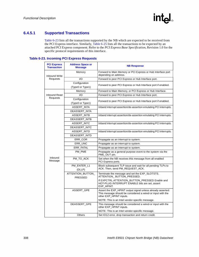
308 Intel® E8501 Chipset North Bridge (NB) Datasheet
Functional Description
6.4.5.1 Supported Transactions
Table 6-23 lists all the transactions supported by the NB which are expected to be received from the PCI Express interface. Similarly, Table 6-25 lists all the transactions to be expected by an attached PCI Express component. Refer to the PCI Express Base Specification, Revision 1.0 for the specific protocol requirements of this interface.
Table 6-23. Incoming PCI Express Requests
PCI Express Transaction
Address Space or Message NB Response
Inbound Write Requests
Memory Forward to Main Memory or PCI Express or Hub Interface port depending on address.
I/O Forward to peer PCI Express or Hub Interface port.Configuration
(Type0 or Type1)Forward to peer PCI Express or Hub Interface port if enabled.
Inbound Read Requests
Memory Forward to Main Memory, or PCI Express or Hub Interface.I/O Forward to peer PCI Express or Hub Interface port.
Configuration(Type0 or Type1)
Forward to peer PCI Express or Hub Interface port if enabled.
Inbound Message
ASSERT_INTA Inband interrupt assertion/de-assertion emulating PCI interrupts. DEASSERT_INTA
ASSERT_INTB Inband interrupt assertion/de-assertion emulating PCI interrupts. DEASSERT_INTB
ASSERT_INTC Inband interrupt assertion/de-assertion emulating PCI interrupts. DEASSERT_INTC
ASSERT_INTD Inband interrupt assertion/de-assertion emulating PCI interrupts. DEASSERT_INTD
ERR_COR Propagate as an interrupt to system. ERR_UNC Propagate as an interrupt to system.
ERR_FATAL Propagate as an interrupt to system. PM_PME Propagate as a general purpose event to the system via the
PME_OUT pin.PM_TO_ACK Set when the NB receives this message from all enabled
PCI Express ports.PM_ENTER_L1
(DLLP)Block subsequent TLP issue and wait for all pending TLPs to ACK. Then, send PM_REQUEST_ACK.
ATTENTION_BUTTON_PRESSED
Terminate the message and set the EXP_SLOTSTS. ATTENTION_ BUTTON_PRESSED. If EXPCTRL.ATTENTION_BUTTON_PRESSED Enable and HOT-PLUG INTERRUPT ENABLE bits are set, assert EXP_HPINT.
ASSERT_GPE Assert the EXP_HPINT output signal unless already asserted. This message should be considered a wired-or input with the other EXP_HPINT inputs.NOTE: This is an Intel vendor-specific message.
DEASSERT_GPE This message should be considered a wired-or input with the other EXP_HPINT inputs.NOTE: This is an Intel vendor-specific message.
Others Set IO12 error, drop transaction and return credit.
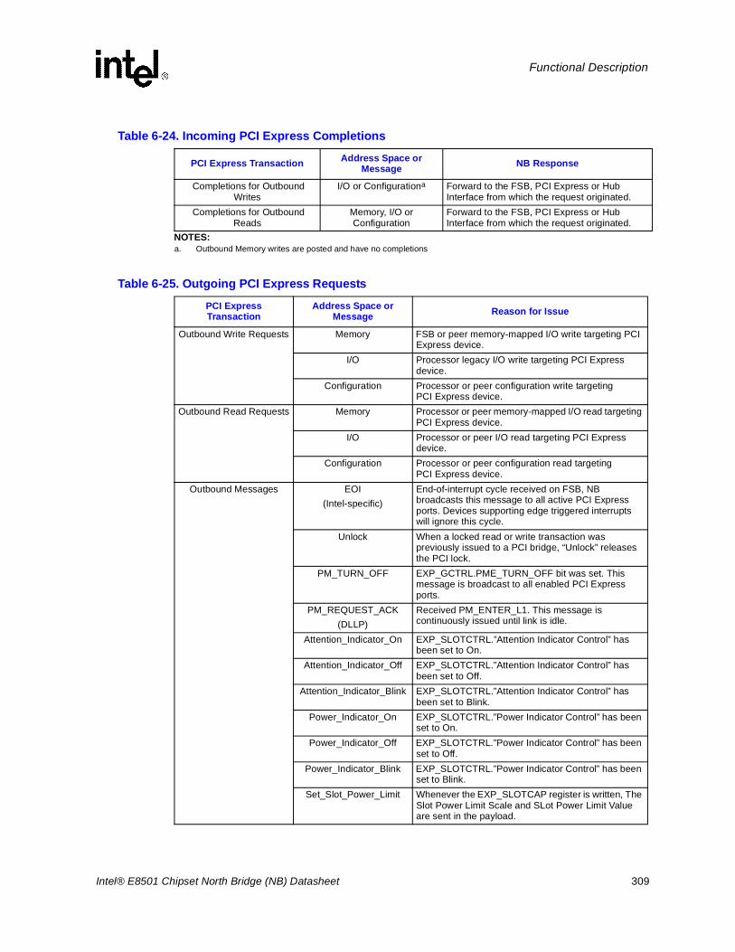
Intel® E8501 Chipset North Bridge (NB) Datasheet 309
Functional Description
Table 6-24. Incoming PCI Express Completions
PCI Express Transaction Address Space or Message NB Response
Completions for Outbound Writes
I/O or Configurationa
NOTES:a. Outbound Memory writes are posted and have no completions
Forward to the FSB, PCI Express or Hub Interface from which the request originated.
Completions for Outbound Reads
Memory, I/O or Configuration
Forward to the FSB, PCI Express or Hub Interface from which the request originated.
Table 6-25. Outgoing PCI Express Requests
PCI Express Transaction
Address Space or Message Reason for Issue
Outbound Write Requests Memory FSB or peer memory-mapped I/O write targeting PCI Express device.
I/O Processor legacy I/O write targeting PCI Express device.
Configuration Processor or peer configuration write targeting PCI Express device.
Outbound Read Requests Memory Processor or peer memory-mapped I/O read targeting PCI Express device.
I/O Processor or peer I/O read targeting PCI Express device.
Configuration Processor or peer configuration read targeting PCI Express device.
Outbound Messages EOI(Intel-specific)
End-of-interrupt cycle received on FSB, NB broadcasts this message to all active PCI Express ports. Devices supporting edge triggered interrupts will ignore this cycle.
Unlock When a locked read or write transaction was previously issued to a PCI bridge, “Unlock” releases the PCI lock.
PM_TURN_OFF EXP_GCTRL.PME_TURN_OFF bit was set. This message is broadcast to all enabled PCI Express ports.
PM_REQUEST_ACK(DLLP)
Received PM_ENTER_L1. This message is continuously issued until link is idle.
Attention_Indicator_On EXP_SLOTCTRL.”Attention Indicator Control” has been set to On.
Attention_Indicator_Off EXP_SLOTCTRL.”Attention Indicator Control” has been set to Off.
Attention_Indicator_Blink EXP_SLOTCTRL.”Attention Indicator Control” has been set to Blink.
Power_Indicator_On EXP_SLOTCTRL.”Power Indicator Control” has been set to On.
Power_Indicator_Off EXP_SLOTCTRL.”Power Indicator Control” has been set to Off.
Power_Indicator_Blink EXP_SLOTCTRL.”Power Indicator Control” has been set to Blink.
Set_Slot_Power_Limit Whenever the EXP_SLOTCAP register is written, The Slot Power Limit Scale and SLot Power Limit Value are sent in the payload.
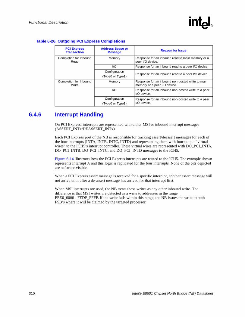
310 Intel® E8501 Chipset North Bridge (NB) Datasheet
Functional Description
6.4.6 Interrupt HandlingOn PCI Express, interrupts are represented with either MSI or inbound interrupt messages (ASSERT_INTx/DEASSERT_INTx).
Each PCI Express port of the NB is responsible for tracking assert/deassert messages for each of the four interrupts (INTA, INTB, INTC, INTD) and representing them with four output “virtual wires” to the ICH5’s interrupt controller. These virtual wires are represented with DO_PCI_INTA, DO_PCI_INTB, DO_PCI_INTC, and DO_PCI_INTD messages to the ICH5.
Figure 6-14 illustrates how the PCI Express interrupts are routed to the ICH5. The example shown represents Interrupt A and this logic is replicated for the four interrupts. None of the bits depicted are software-visible.
When a PCI Express assert message is received for a specific interrupt, another assert message will not arrive until after a de-assert message has arrived for that interrupt first.
When MSI interrupts are used, the NB treats these writes as any other inbound write. The difference is that MSI writes are detected as a write to addresses in the rangeFEE0_0000 - FEDF_FFFF. If the write falls within this range, the NB issues the write to both FSB’s where it will be claimed by the targeted processor.
Table 6-26. Outgoing PCI Express Completions
PCI Express Transaction
Address Space or Message Reason for Issue
Completion for Inbound Read
Memory Response for an inbound read to main memory or a peer I/O device.
I/O Response for an inbound read to a peer I/O device.Configuration
(Type0 or Type1)Response for an inbound read to a peer I/O device.
Completion for Inbound Write
Memory Response for an inbound non-posted write to main memory or a peer I/O device.
I/O Response for an inbound non-posted write to a peer I/O device.
Configuration (Type0 or Type1)
Response for an inbound non-posted write to a peer I/O device.
Intel® E8501 Chipset North Bridge (NB) Datasheet 311
Functional Description
6.4.7 Ordering RulesThis section describes the NB ordering rules for transactions progressing through the PCI Express unit.
6.4.7.1 Inbound Transaction Ordering Rules
Inbound transactions originate from PCI Express and target main memory. In general, the PCI Express cluster holds inbound transactions in FIFO order. There are exceptions to this order under certain situations. For example, PCI Express requires that read completions are allowed to pass read requests. This forces any read completions to bypass any reads which might be back pressured in the queue. The PCI Express ports have no ordering relationship to each other (aside from the peer-to-peer restrictions below).
Sequential, non-posted requests are not required to be completed in the order they were requested. However, if a non-posted request requires multiple sub-completions (typically due to splitting a memory read into cacheline requests), then those sub-completions must be delivered in order.
Inbound writes cannot be posted beyond the PCI Express domain and outbound writes may only be posted after the write is acknowledged by the destination PCI Express cluster. The posting of writes relies on the fact that the system maintains a certain ordering relationship. Since the NB cannot post inbound writes beyond the PCI Express cluster, the NB must wait for snoop responses before issuing subsequent, order-dependent transactions.
Figure 6-14. Legacy Interrupt Routing (INTA Example)
DO_PCI_INTA(to ICH)
1 0 0 0 1 1 0
312 Intel® E8501 Chipset North Bridge (NB) Datasheet
Functional Description
6.4.7.2 Inbound Ordering Requirements
In general, there are no ordering requirements between transactions issued on the different PCI Express interfaces. However, the below rules apply to inbound transactions issued on the same interface.
The following rules must be ensured for inbound transactions:
Inbound messages are listed in Table 6-23. Similarly to inbound posted writes, reads should push these commands ahead.
The above rules apply whether the transaction is coherent or non-coherent. Some regions of memory space are considered non-coherent (e.g. the Don’t Snoop attribute is set). The PIQ will order all transactions regardless of its destination.
6.4.7.3 Outbound Transaction Ordering Rules
Outbound transactions through the NB are memory, I/O or configuration read/write transactions originating on a processor interface destined for a PCI Express device. Subsequent outbound transactions with different destinations have no ordering requirements between them. Multiple transactions destined for the same PCI Express port are ordered according to the ordering rules specified in PCI Express Base Specification, Revision 1.0.
RULE 1: Outbound non-posted read and write completions must be allowed to progress past stalled inbound non-posted requests.
RULE 2: Inbound posted write requests must be allowed to progress past stalled inbound non-posted requests.
RULE 3: Inbound posted write requests, inbound read requests, outbound non-posted read and write completions cannot pass enqueued inbound posted write requests.
RULE 4: The Producer - Consumer model, prevents read requests, write requests, and non-posted read or write completions from passing write requests.
RULE 5: Outbound non-posted read or write completions must push ahead all prior inbound posted write transactions from that PCI Express port.
RULE 6: To optimize performance, inbound, coherent, posted writes will issue ownership requests (RFO) without waiting for prior ownership requests to complete.
RULE 7: Inbound messages follow the same ordering rules as inbound posted writes.
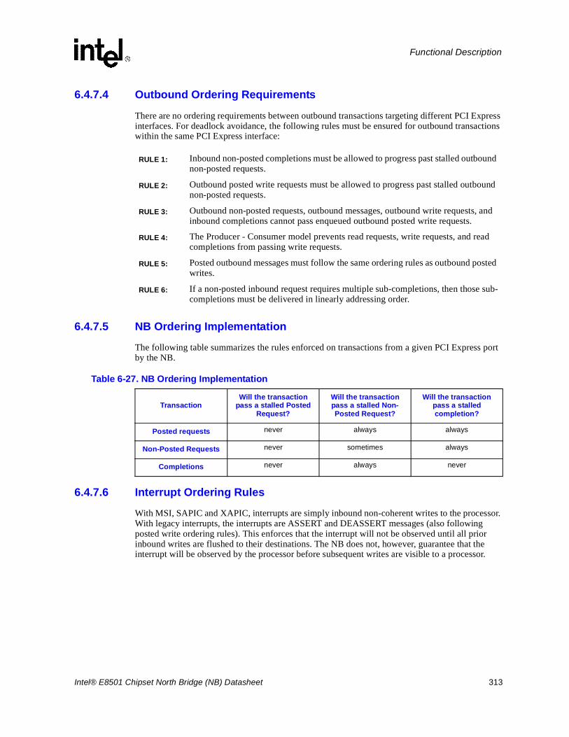
Intel® E8501 Chipset North Bridge (NB) Datasheet 313
Functional Description
6.4.7.4 Outbound Ordering Requirements
There are no ordering requirements between outbound transactions targeting different PCI Express interfaces. For deadlock avoidance, the following rules must be ensured for outbound transactions within the same PCI Express interface:
6.4.7.5 NB Ordering Implementation
The following table summarizes the rules enforced on transactions from a given PCI Express port by the NB.
6.4.7.6 Interrupt Ordering Rules
With MSI, SAPIC and XAPIC, interrupts are simply inbound non-coherent writes to the processor. With legacy interrupts, the interrupts are ASSERT and DEASSERT messages (also following posted write ordering rules). This enforces that the interrupt will not be observed until all prior inbound writes are flushed to their destinations. The NB does not, however, guarantee that the interrupt will be observed by the processor before subsequent writes are visible to a processor.
RULE 1: Inbound non-posted completions must be allowed to progress past stalled outbound non-posted requests.
RULE 2: Outbound posted write requests must be allowed to progress past stalled outbound non-posted requests.
RULE 3: Outbound non-posted requests, outbound messages, outbound write requests, and inbound completions cannot pass enqueued outbound posted write requests.
RULE 4: The Producer - Consumer model prevents read requests, write requests, and read completions from passing write requests.
RULE 5: Posted outbound messages must follow the same ordering rules as outbound posted writes.
RULE 6: If a non-posted inbound request requires multiple sub-completions, then those sub-completions must be delivered in linearly addressing order.
Table 6-27. NB Ordering Implementation
TransactionWill the transaction
pass a stalled Posted Request?
Will the transaction pass a stalled Non-Posted Request?
Will the transaction pass a stalled completion?
Posted requests never always always
Non-Posted Requests never sometimes always
Completions never always never
314 Intel® E8501 Chipset North Bridge (NB) Datasheet
Functional Description
6.4.8 Hot-PlugEach PCI Express port supports the optional Hot-Plug capability described in PCI Express Base Specification, Revision 1.0. The PCI Express Hot-Plug model implies a Hot-Plug controller per port which is identified to software as a capability of the P2P Bridge configuration space.
PCI Express Hot-Plug support requires that the NB supports a set of Hot-Plug messages (listed in Table 6-23 and Table 6-25) to manage the states between the Hot-Plug controller and the device.
The PCI Express form factor has an impact to the level of support required of the NB. For example, some of the Hot-Plug messages are required only if the LED indicators reside on the actual card and are accessed through the endpoint device (SIOM). The NB supports all of the Hot-Plug messages so that the platform is not constrained to any particular form factor.
Hot-Plug Controller:
PCI Express Hot-Plug requires that the NB implements a Hot-Plug controller for every Hot-Pluggable interface. The Hot-Plug controller is a capability of the bridge configuration space and the register set is accessible through the standard PCI capability mechanism defined in PCI Express Base Specification, Revision 1.0.
6.4.8.1 PCI Express Add-in Card Hot-Plug Model
The subsections below describe the signals required for PCI Express Add-in Card Hot-Plug. This model is such that the LEDs and remove button reside on the chassis. The NB provides an SMBus interface to a set of external programmable I/O devices that provide the Hot-Plug pins for any PCI Express ports that support Hot-Plug. This interface is described in Section 6.6.
6.4.8.2 Hot-Plug Pins
Table 6-28 describes the Hot-Plug signals used for Hot-Plug. For registers that control or provide the status of these pins please refer to Section 4.16.8, “GLOBAL_FERR: Global First Error Register (D16, F2)” on page 196.
Table 6-28. Hot-Plug Pins
Signal Name Description
ATNLED# This indicator is connected to the Attention LED on the baseboard.
PWRLED# This indicator is connected to the Power LED on the baseboard.
BUTTON# Input signal per slot which indicates that the user wishes to hot remove or hot add a PCI Express card.
PRSNT# Input signal that indicates if a “Hot-Plugged” PCI Express device is currently plugged into the slot.
PWRFLT# Input signal from the power controller to indicate that a power fault has occurred.
PWREN Output signal allowing software to enable or disable a PCI Express slot.
EXP_HPINT Hot-Plug interrupt output signal. There is only one EXP_HPINT signal for the NB. Both parallel interfaces drive the same output signal.
MRL#Manual (mechanical) Retention Latch input indicates that a retention latch is enabled or disabled on the board for this slot. A retention latch is used on the platform to mechanically hold the card in place.
Intel® E8501 Chipset North Bridge (NB) Datasheet 315
Functional Description
6.4.8.3 SIOM Hot-Plug Model
The SIOM Hot-Plug model is such that the LEDs and remove button reside on the endpoint module. Because of this model, the NB is responsible for issuing in-band messages to the endpoint and the endpoint is responsible for controlling the button, LEDs, etc.
The messages used for the SIOM Hot-Plug model are listed in Table 6-23 and Table 6-25 and describe the behavior of the button and LEDs.
6.5 Hub Interface 1.5 - (Compatibility Interface)The HI1.5 is an 8-bit port responsible for accepting and sending packets between the NB and the ICH5 component.
6.5.1 Physical LayerThe compatibility interface supports parallel termination. Parallel termination is required for the routing distances required for Intel® E8501 chipset chipset-based platforms. Hub Interface uses a point-to-point bus topology using a combination of common clock framing signals and source-synchronous data transfer. The 8-bit data bus rate is 266 MHz (quad-pumped) using strobe signals. This interface is protected with one parity bit per 32 bits of data.
6.5.2 Transaction LayerTable 6-29 lists all the transactions supported by the NB which are expected to be received from the ICH5. Similarly, Table 6-31 lists all the transactions to be expected by the ICH5. Refer to the I/O Controller Hub5 (ICH5), I/O Controller Hub5-M Datasheet for the specific protocol requirements of this interface.
Table 6-29. Incoming Hub Interface Request Cycles
Hub Interface Transaction Transaction Type NB Response
Inbound Write Requests
Memory Forward to Main Memory or PCI Express port depending on address.
Inbound Read Requests
Memory Forward to Main Memory or PCI Express.
Inbound Special Cycles
Go C0 Ignore. No further action is taken.
Go C3 Immediately respond with an “ACK C3” special cycle. No further action is taken.
Go C3A Immediately respond with an “ACK C3A” special cycle. No further action is taken.
APIC Interrupt xmit requested
Since this chipset does not support the serial APIC bus, this special cycle is simply responded to with an “APIC Interrupt xmit granted” special cycle.
SRC Special Reserved Cycle. This command is used for supporting parallel termination. This command is sent when the I/O bridge wants to do an RCOMP calculation. The NB stays off the bus for the duration indicated by the length but otherwise ignores this cycle.
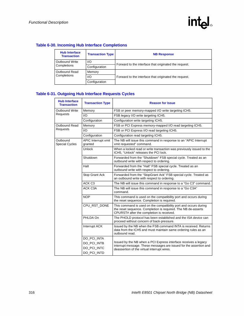
316 Intel® E8501 Chipset North Bridge (NB) Datasheet
Functional Description
Table 6-30. Incoming Hub Interface Completions
Hub Interface Transaction Transaction Type NB Response
Outbound Write Completions
I/OForward to the interface that originated the request.
ConfigurationOutbound Read Completions
MemoryForward to the interface that originated the request.I/O
Configuration
Table 6-31. Outgoing Hub Interface Requests Cycles
Hub Interface Transaction Transaction Type Reason for Issue
Outbound Write Requests
Memory FSB or peer memory-mapped I/O write targeting ICH5.I/O FSB legacy I/O write targeting ICH5.Configuration Configuration write targeting ICH5.
Outbound Read Requests
Memory FSB or PCI Express memory-mapped I/O read targeting ICH5.I/O FSB or PCI Express I/O read targeting ICH5.Configuration Configuration read targeting ICH5.
OutboundSpecial Cycles
APIC Interrupt xmit granted
The NB will issue this command in response to an “APIC Interrupt xmit requested” command.
Unlock When a locked read or write transaction was previously issued to the ICH5, “Unlock” releases the PCI lock.
Shutdown Forwarded from the “Shutdown” FSB special cycle. Treated as an outbound write with respect to ordering.
Halt Forwarded from the “Halt” FSB special cycle. Treated as an outbound write with respect to ordering.
Stop Grant Ack Forwarded from the “StopGrant Ack” FSB special cycle. Treated as an outbound write with respect to ordering.
ACK C3 The NB will issue this command in response to a “Go C3” command.ACK C3A The NB will issue this command in response to a “Go C3A”
command.NOP This command is used on the compatibility port and occurs during
the reset sequence. Completion is required.CPU_RST_DONE This command is used on the compatibility port and occurs during
the reset sequence. Completion is required. The NB de-asserts CPURST# after the completion is received.
PHLDA On The PHOLD protocol has been established and the ISA device can proceed without concern of back-pressure.
Interrupt ACK Issued by the NB when the FSB command INTA is received. Returns data from the ICH5 and must maintain same ordering rules as an outbound read.
DO_PCI_INTADO_PCI_INTBDO_PCI_INTCDO_PCI_INTD
Issued by the NB when a PCI Express interface receives a legacy interrupt message. These messages are issued for the assertion and deassertion of the virtual interrupt wires.
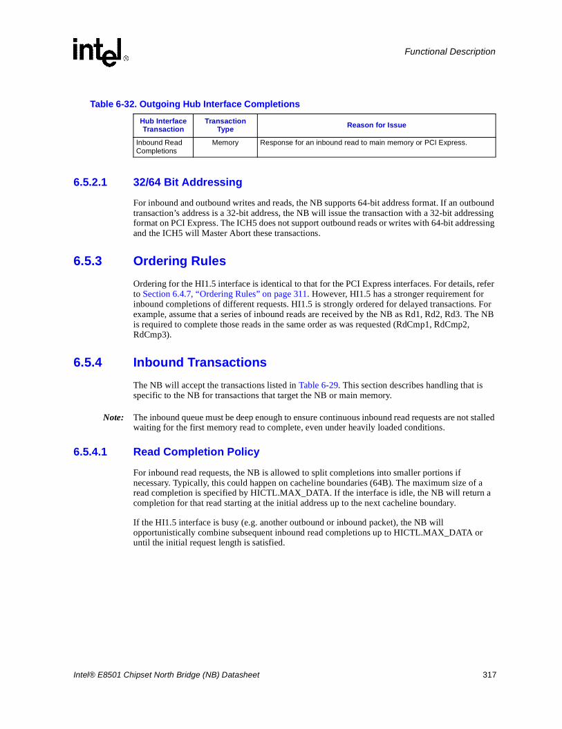
Intel® E8501 Chipset North Bridge (NB) Datasheet 317
Functional Description
6.5.2.1 32/64 Bit Addressing
For inbound and outbound writes and reads, the NB supports 64-bit address format. If an outbound transaction’s address is a 32-bit address, the NB will issue the transaction with a 32-bit addressing format on PCI Express. The ICH5 does not support outbound reads or writes with 64-bit addressing and the ICH5 will Master Abort these transactions.
6.5.3 Ordering RulesOrdering for the HI1.5 interface is identical to that for the PCI Express interfaces. For details, refer to Section 6.4.7, “Ordering Rules” on page 311. However, HI1.5 has a stronger requirement for inbound completions of different requests. HI1.5 is strongly ordered for delayed transactions. For example, assume that a series of inbound reads are received by the NB as Rd1, Rd2, Rd3. The NB is required to complete those reads in the same order as was requested (RdCmp1, RdCmp2, RdCmp3).
6.5.4 Inbound TransactionsThe NB will accept the transactions listed in Table 6-29. This section describes handling that is specific to the NB for transactions that target the NB or main memory.
Note: The inbound queue must be deep enough to ensure continuous inbound read requests are not stalled waiting for the first memory read to complete, even under heavily loaded conditions.
6.5.4.1 Read Completion Policy
For inbound read requests, the NB is allowed to split completions into smaller portions if necessary. Typically, this could happen on cacheline boundaries (64B). The maximum size of a read completion is specified by HICTL.MAX_DATA. If the interface is idle, the NB will return a completion for that read starting at the initial address up to the next cacheline boundary.
If the HI1.5 interface is busy (e.g. another outbound or inbound packet), the NB will opportunistically combine subsequent inbound read completions up to HICTL.MAX_DATA or until the initial request length is satisfied.
Table 6-32. Outgoing Hub Interface Completions
Hub Interface Transaction
Transaction Type Reason for Issue
Inbound Read Completions
Memory Response for an inbound read to main memory or PCI Express.
318 Intel® E8501 Chipset North Bridge (NB) Datasheet
Functional Description
6.5.4.2 Inbound Write Transactions
Note: This section applies to all write transactions targeting DRAM.
Inbound coherent write transactions actually comprise two operations:
1. Request for ownership
2. Cache line write (mark to Modified state)
The compatibility interface will enqueue each inbound write as a single atomic instruction. As the compatibility interface enqueues the write, it will also bypass all queues by sending a request-for-ownership command (RFO) directly to the FSB’s requesting line ownership. The RFO commands are allowed to be issued in any order.
If the NB owns the line after all inbound ordering rules have been met, the write command proceeds and the line is modified. If the line is not owned by the NB after all inbound ordering rules have been met, the write is temporarily stalled until ownership is acquired and requests will continue to fill the inbound queue. When the request for ownership completes, the write command is forwarded where the line is marked in the Modified state.
Note: Because of the HI1.5 ordering rules, transactions after an inbound write must wait until after the write is globally visible. The inbound queue must be deep enough to ensure that continuous inbound traffic is not stalled waiting for the above write sequence, even under heavily loaded conditions.
6.5.4.3 Inbound Write Combining
The NB performs write combining opportunistically in the on-chip CDC. If a write is issued to memory and the NB owns the line, the data buffer will overwrite the buffer with the new data (full or partial data).
6.5.4.4 PHOLD Support
The NB supports the PHOLD protocol. This protocol is used for legacy ISA devices which did not allow for the possibility of being both a master and a slave device simultaneously. Example devices that use the PHOLD protocol are legacy floppy drives and parallel port DMA.
6.5.5 Outbound TransactionsThe NB will generate the outbound transactions listed in Table 6-31. This section describes handling that is specific to the NB for transactions that target the ICH5.
6.5.5.1 Outbound Non-posted Transactions
Non-posted transactions that the NB propagates includes Interrupt Acknowledge, memory reads, I/O reads and writes, and configuration reads and writes. When a non-posted transaction is issued from the NB, the ICH5 device will respond with a completion.
The ICH5 supports only one outstanding non-posted transaction comprising transactions issued by the processors or a peer PCI Express device.
Intel® E8501 Chipset North Bridge (NB) Datasheet 319
Functional Description
6.5.5.2 Stalled Non-posted Requests
Non-posted requests are non-blocking transactions. In other words, while a non-posted request is pending, subsequent transactions are required to bypass the transactions which are waiting for a completion.
6.5.5.3 Outbound Posted Transactions
Once a posted request (e.g. memory write) is issued from HI1.5, the request is considered to be complete and the transaction is removed from the outbound queue. For posted requests, the acknowledge has already been sent to the initiating interface (FSB or alternate PCI Express inbound queue) when the write was enqueued in the outbound PCI Express unit, so proper ordering is guaranteed.
6.5.5.4 Outbound Write Combining
The NB does not combine sequential outbound writes. This optimization is left to the processor write combining buffers.
6.5.5.5 Lock Support
For legacy PCI functionality, the NB supports bus locks through an explicit sequence of events. The NB can receive a locked transaction sequence (Read-Write or Read-Read-Write-Write) on a FSB directed to the ICH5. The compatibility interface cluster must support the following capabilities:
• Retry all transactions on the Hub Interface
• Generate a locked read request to the Hub Interface target
• Unlock a locked Hub Interface port
6.5.6 Peer-to-Peer SupportPeer-to-peer support is defined as transactions which initiate on one I/O interface and target another without going through main memory. This support applies to both PCI Express and HI. The NB supports peer-to-peer transactions for memory and I/O transactions. The compatibility interface can be the destination of a peer-to-peer write or read. The compatibility interface can be the source of a posted peer-to-peer write. Non-posted requests may pre-fetch into MMIO (with potential side effects). Peer-to-peer transactions are not observed on any interface except the target and destination (e.g. no FSB snoops).
Peer-to-peer traffic between the PCI Express ports and the ICH5 must sustain the full write bandwidth. For reads, full bandwidth is required for large request sizes. Inbound coherent transactions and peer-to-peer transactions must maintain ordering rules between each other. Peer-to-peer transactions follow inbound ordering rules until it reaches the head of the inbound queue. Once the transaction reaches the head of the inbound queue, the NB routes the transaction to the next available slot in the outbound queue where PCI ordering is maintained until the end of the transaction. The NB does not support peer-to-peer where the source and destination is the same PCI Express Interface.
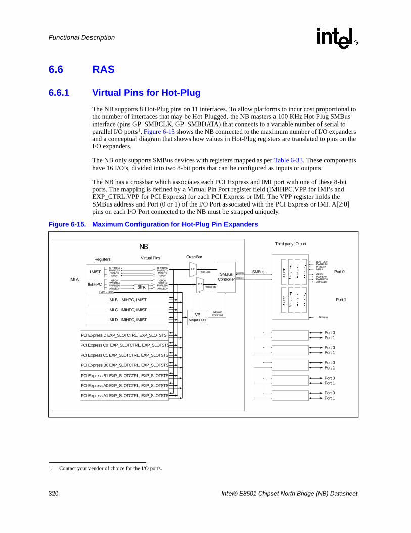
320 Intel® E8501 Chipset North Bridge (NB) Datasheet
Functional Description
6.6 RAS
6.6.1 Virtual Pins for Hot-PlugThe NB supports 8 Hot-Plug pins on 11 interfaces. To allow platforms to incur cost proportional to the number of interfaces that may be Hot-Plugged, the NB masters a 100 KHz Hot-Plug SMBus interface (pins GP_SMBCLK, GP_SMBDATA) that connects to a variable number of serial to parallel I/O ports1. Figure 6-15 shows the NB connected to the maximum number of I/O expanders and a conceptual diagram that shows how values in Hot-Plug registers are translated to pins on the I/O expanders.
The NB only supports SMBus devices with registers mapped as per Table 6-33. These components have 16 I/O’s, divided into two 8-bit ports that can be configured as inputs or outputs.
The NB has a crossbar which associates each PCI Express and IMI port with one of these 8-bit ports. The mapping is defined by a Virtual Pin Port register field (IMIHPC.VPP for IMI’s and EXP_CTRL.VPP for PCI Express) for each PCI Express or IMI. The VPP register holds the SMBus address and Port (0 or 1) of the I/O Port associated with the PCI Express or IMI. A[2:0] pins on each I/O Port connected to the NB must be strapped uniquely.
1. Contact your vendor of choice for the I/O ports.
Figure 6-15. Maximum Configuration for Hot-Plug Pin Expanders
IMI A
VPP + HPC
Blink
SMBusController
Registers Virtual Pins
PWRCTL#PWRLED#ATNLED#
PWRFLT#PRSNT#
MRL#
BUTTON#
GPO#
1:11
11:1
Read Data
Write Data
IMI B IMIHPC, IMIST
CrossBar
VPsequencer
SMBCLK
SMBDATA SMBus
NB Third party IO port
PWREN#PWRLED#ATNLED#
PWRFLT#PRSNT#
MRL#
BUTTON#
GPO#PWREN#PWRLED#ATNLED#
PWRFLT#PRSNT#MRL#
BUTTON#
GPO#Port 0
Port 1
Address
Port 0Port 1
Port 0Port 1
Port 0Port 1
Port 0Port 1
Port 0Port 1
PCI Express D EXP_SLOTCTRL, EXP_SLOTSTS
Adrs andCommand
IMIHPC
IMIST
IMI C IMIHPC, IMIST
IMI D IMIHPC, IMIST
PCI Express C0 EXP_SLOTCTRL, EXP_SLOTSTS
PCI Express C1 EXP_SLOTCTRL, EXP_SLOTSTS
PCI Express B0 EXP_SLOTCTRL, EXP_SLOTSTS
PCI Express B1 EXP_SLOTCTRL, EXP_SLOTSTS
PCI Express A0 EXP_SLOTCTRL, EXP_SLOTSTS
PCI Express A1 EXP_SLOTCTRL, EXP_SLOTSTS
Intel® E8501 Chipset North Bridge (NB) Datasheet 321
Functional Description
6.6.1.1 Operation
When the NB comes out of reset, the I/O ports are inactive. The NB is not aware of how many I/O Ports are connected to it, what their addresses are, nor what PCI Express or IMI ports are Hot-Pluggable. The NB does not master any commands on the SMBus until a Hot-Plug Capable bit is set.
An IMI port is considered Hot-Plug Capable when IMIHPC.HPC bit is set. A PCI Express port is considered Hot-Plug Capable when EXP_SLOTCAP.HPC bit and EXP_CTRL.EN_VPP are set. When a port is considered Hot-Plug Capable, the NB initializes the associated VPP with Direction and Logic Level configuration as shown in Table 6-34. The polarity is left at the default values and never written. When writing to VPP registers outside the NB, addresses are used as described in Table 6-35 for writes to the VPP registers connected to the I2C port.
When the NB is not responding to a change in whether a port is Hot-Plug Capable, it performs input register reads and output register writes to all the Hot-Plug Capable VPP’s. This sequence repeats indefinitely until there is a change in whether a port is Hot-Plug Capable. To minimize the completion time of this sequence and its complexity, both ports are always read and written. For the maximum number of 6 I/O ports, and assuming no clock stretching, this sequence can take up to 51 ms. If new Hot-Plug capability bits are not being set, this is the maximum timing uncertainty in sampling or driving these signals.
Table 6-33. I/O Port Registers Supported by Intel® E8501 Chipset North Bridge (NB)
Register Name Intel® E8501 chipset north bridge (NB) Usage
0 Input Port 0 Continuously Reads Input Values
1 Input Port 1
2 Output Port 0 Continuously Writes Output Values
3 Output Port 1
4 Polarity Inversion Port 0 Never written by NB
5 Polarity Inversion Port 1
6 Configuration Port 0 Direction set as per Table 6-34
7 Configuration Port 1
Table 6-34. Hot-Plug Signals on a Virtual Pin Port (VPP) (Sheet 1 of 2)
BitPresent for
Direction Logic Level Polarity SignalPCI Express IMI
0 Yes Yes Output 1 true ATNLED#
1 Yes Yes Output 1 true PWRLED#
2 Yes Yes Input 1 true BUTTON#
3 Yes Yes Input 1 true PWRFLT#
4 Yes Yes Input 1 true PRSNT#
322 Intel® E8501 Chipset North Bridge (NB) Datasheet
Functional Description
Table 6-35 describes the sequence generated for a write to an I/O port. Both 8-bit ports are always written. If a VPP is valid for the 8-bit port, the Output values are updated as per the IMIHPC or the EXP_SLOTCTRL registers for the associated IMI or the PCI Express Hot-Plug registers. The Input values affect the IMIST and PCI Express Hot-Plug registers. If no VPP for the 8-bit port is valid, 0s are written.
The NB issues Read Commands to update NB virtual inputs from the I/O Port. The I/O port requires that a command be sent to sample the inputs, then another command is issued to return the data. The NB always reads inputs from both 8-bit ports. If the VPP is valid, the NB updates the associated MIHPS (for IMI) or the EXP_SLOTSTS (for PCI Express) register according to the values of BUTTON#, PWRFLT#, and PRSNT# read from the value register in the I/O Port. Results from invalid VPP’s are discarded. Table 6-36 defines the read command format.
5 Yes Yes Output 1 true PWREN#
6 Yes Yes Input 1 true MRL#
7 No Yes Input 1 true PWRGOOD
Table 6-34. Hot-Plug Signals on a Virtual Pin Port (VPP) (Sheet 2 of 2)
BitPresent for
Direction Logic Level Polarity SignalPCI Express IMI
Table 6-35. VPP Write Command
Bits NB Drives I/O Port Drives Comment
1 Start SDL (Serial Data Line) falling followed by SCL (Serial Clock Line) falling
7 Address[6:0] [6:3] = 0100[2:0] = VPP[3:1]
1 0 indicates write
1 ACK If NACK is received, NB completes with stop and sets Error T9
8 Register Number Register Address see Table 6-33[2:1] = 01 for Output, 11 for Direction[0] = 0
1 ACK If NACK is received, NB completes with stop and sets Error T9
8 Data One bit for each bit of port 0 as per Table 6-34
1 ACK If NACK is received, NB completes with stop and sets Error T9
8 Data One bit for each bit of port 1 as per Table 6-34
1 ACK If NACK is received, NB completes with stop and sets Error T9
1 Stop
Intel® E8501 Chipset North Bridge (NB) Datasheet 323
Functional Description
If a VPP register is set to a non-existent address, it will not acknowledge the command and the NB will set the T9 error. The NB will continue to address the existing devices.
6.6.1.2 Limitations
This interface is dedicated to Hot-Plug and does not support aspects of SMBus that are not required for this application.
Table 6-36. VPP Read Command
Bits NB Drives I/O Port Drives Comment
1 Start SDL falling followed by SCL falling
7 Address[6:0] [6:3] = 0100[2:0] = VPP[3:1]
1 0 Indicates Write
1 ACK If NACK is received, NB completes with stop and sets Error T9
8 RegisterNumber[2:0] Register Address [2:1] = 00
[0] = 0
1 ACK If NACK is received, NB completes with stop and sets Error T9
1 Start SDL falling followed by SCL falling
7 Address[6:0] [6:3] = 0100[2:0] = VPP[3:1]
1 1 Indicates Read
1 ACK If NACK is received, NB completes with stop and sets Error T9
8 Data One bit for each bit of port 1 as per Table 6-34. The NB always reads from both ports. Results for invalid VPP’s are discarded
1 ACK
8 Data One bit for each bit of port 1 as shown in Table 6-34. The NB always reads from both ports. Results for invalid VPP’s are discarded
1 NACK
1 Stop
Table 6-37. Unsupported Aspects of SMBus
Unsupported Aspect Comment
Command sequences not defined in this specification
Such as Block reads, Process Calls, Host Notification, etc.
Arbitration NB is the only master.
PEC The targeted I/O Ports do not support it.
Bus Enumeration BIOS is required to configure VPP’s with this information. Variation in the number of devices is not supported for a particular platform.
Clock Stretching NB will drive 100 KHz and I/O Ports can support higher frequencies, so they will never stretch the clock.
NACK Retry SMBus forbids devices from NACK’ing if they are busy.
324 Intel® E8501 Chipset North Bridge (NB) Datasheet
Functional Description
6.7 Error ReportingThe NB recognizes a variety of errors (or exception conditions) and is the collection point for many of these errors. Some errors are internally detected and others are signaled to it from the external interfaces (PCI Express and IMI). All detected errors eventually cause the NB to do one of the following:
• Assert MCERR on both FSB’s
• Assert Error pins (ERR[2:0])
The error reporting for the NB is comprised of the status registers (FERR and NERR), the error log registers (recoverable and non-recoverable), and the error pins (ERR[2:0]). The individual errors can be programmed to be masked or to be signaled by ERR[2:0] or by MCERR.
6.7.1 Error TypesThe errors can be classified into three types: (1) Correctable errors, (2) Uncorrectable Errors, (3) Hardware Fatal errors. The discussion here assumes that for all these error types, hardware provides the capability to detect the error. Errors that cannot be detected by hardware cause silent data corruption, which is an undesirable event.
• Correctable Errors are corrected by the hardware and software is completely oblivious to this event. Examples of such errors include single bit ECC errors and successful link level retry. Such events may be logged and reported by the system for a post-mortem by the firmware or system management software.
• Uncorrectable Errors are not corrected by the hardware or software. OS or other software layers may be able to recover from such errors, but it may not always be possible. Such errors are typically contained in nature, the system state is intact, and the process and the system is restartable. Errors in this category include multi-bit data error, transaction time out, and so on.
• Fatal Errors may compromise system integrity and continued operation may not be possible. Errors in this category include protocol errors.
6.7.2 Error Mask and Signaling Mapping RegisterEach error is defined to be a recoverable or non-recoverable error. This determines which FERRST, NERRST, and log register get used in reporting the error. In addition, the error also has an Error Mask and Signaling registers. The purpose of the error mask is to mask / allow the observance of the error condition. Each local block has an error mask for the errors detected in that particular block.
Each unmasked error can generally be programmatically routed to the following error signals:
• MCERR
• ERR[2], ERR[1], or ERR[0]
• ICHRST
Note: It is up to software to enable only one of the error signaling possibilities (MCERR, ERR[2], ERR[1] & ERR[0], ICHRST signals). Software should not map PCI Express errors to the MCERR signal.
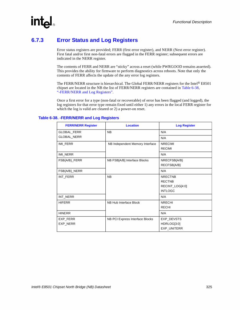
Intel® E8501 Chipset North Bridge (NB) Datasheet 325
Functional Description
6.7.3 Error Status and Log RegistersError status registers are provided; FERR (first error register), and NERR (Next error register). First fatal and/or first non-fatal errors are flagged in the FERR register; subsequent errors are indicated in the NERR register.
The contents of FERR and NERR are “sticky” across a reset (while PWRGOOD remains asserted). This provides the ability for firmware to perform diagnostics across reboots. Note that only the contents of FERR affects the update of the any error log registers.
The FERR/NERR structure is hierarchical. The Global FERR/NERR registers for the Intel® E8501 chipset are located in the NB the list of FERR/NERR registers are contained in Table 6-38, “-FERR/NERR and Log Registers”.
Once a first error for a type (non-fatal or recoverable) of error has been flagged (and logged), the log registers for that error type remain fixed until either 1) any errors in the local FERR register for which the log is valid are cleared or 2) a power-on reset.
Table 6-38. -FERR/NERR and Log Registers
FERR/NERR Register Location Log Register
GLOBAL_FERRGLOBAL_NERR
NB N/A
N/A
IMI_FERR NB Independent Memory Interface NRECIMIRECIMI
IMI_NERR N/A
FSB{A/B}_FERR NB FSB[A/B] Interface Blocks NRECFSB{A/B}RECFSB{A/B}
FSB{A/B}_NERR N/A
INT_FERR NB NRECTNBRECTNBRECINT_LOG[4:0]INTLOGC
INT_NERR N/A
HIFERR NB Hub Interface Block NRECHIRECHI
HINERR N/A
EXP_FERREXP_NERR
NB PCI Express Interface Blocks EXP_DEVSTSHDRLOG[3:0]EXP_UNITERR
326 Intel® E8501 Chipset North Bridge (NB) Datasheet
Functional Description
6.7.4 Error Signaling
Associated with each pair of FERR/NERR registers are three open drain error pins, one for each error type: fatal, uncorrectable and correctable (ERR#[2:0]). If not masked (EMASK register), these pins will reflect the error status for each type of error in the two error status registers. The NB can signal errors via the following pins:
• Err[0] - Correctable Errors (Non-Fatal or Recoverable Error)
• Err[1] - Uncorrectable Errors (Non-Fatal or Recoverable Error)
• Err[2] - Fatal Error
• MCERR- Adhering to the FSB rules for driving MCERR.
The error pins are I/O signals that are synchronous to the 166 MHz bus clock.
6.7.5 Error Integration into Intel® E8501 Chipset North Bridge (NB) Error ModelRefer to Figure 6-5 for how the PCI Express errors map into the NB error registers and for how the flow of error detection and logging is handled inside the NB.
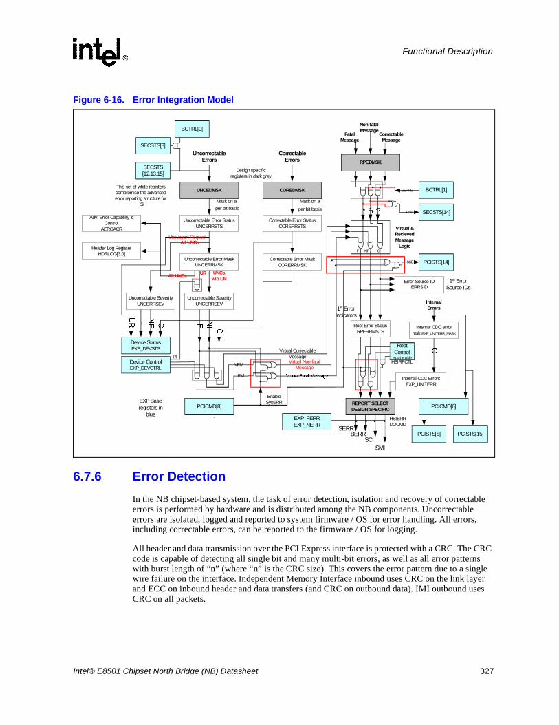
Intel® E8501 Chipset North Bridge (NB) Datasheet 327
Functional Description
6.7.6 Error DetectionIn the NB chipset-based system, the task of error detection, isolation and recovery of correctable errors is performed by hardware and is distributed among the NB components. Uncorrectable errors are isolated, logged and reported to system firmware / OS for error handling. All errors, including correctable errors, can be reported to the firmware / OS for logging.
All header and data transmission over the PCI Express interface is protected with a CRC. The CRC code is capable of detecting all single bit and many multi-bit errors, as well as all error patterns with burst length of “n” (where “n” is the CRC size). This covers the error pattern due to a single wire failure on the interface. Independent Memory Interface inbound uses CRC on the link layer and ECC on inbound header and data transfers (and CRC on outbound data). IMI outbound uses CRC on all packets.
Figure 6-16. Error Integration Model
Uncorrectable Error MaskUNCERRMSK
Correctable Error StatusCORERRSTS
Correctable Error MaskCORERRMSK
Uncorrectable SeverityUNCERRSEV
EnableSysERR
Mask on aper bit basis
FatalMessage
UncorrectableErrors
CorrectableErrors
CorrectableMessage
Non-fatalMessage
Device StatusEXP_DEVSTS
Device ControlEXP_DEVCTRL
EXP Baseregisters in
bluePCICMD[8]
Mask on aper bit basis
Virtual CorrectableMessageVirtual Non-fatal
Message
Adv. Error Capability &Control
AERCACR
Header Log RegisterHDRLOG[3:0]
Uncorrectable Error StatusUNCERRSTS
This set of white registerscompromise the advancederror reporting structure for
HSI
UNCEDMSK COREDMSK
Uncorrectable SeverityUNCERRSEV
All UNCs
Root Error StatusRPERRMSTS
Error Source IDERRSID
REPORT SELECTDESIGN SPECIFIC
BERRSCI
SMI
RootControl
report enable
1st ErrorIndicators
1st ErrorSource IDs
HSIRPCTL
HSIERRDOCMD
Design specificregisters in dark grey
SERR
NFM
FM
BCTRL[1]SERRE
Virtual &RecievedMessage
Logic
SECSTS[14]RSE
All UNCs
Unsupport Request
UR
[3]
PCISTS[14]SSE
F NF C
UNCsw/o UR
SECSTS[12,13,15]
SECSTS[8]
BCTRL[0]
EXP_FERREXP_NERR
RPEDMSK
Internal CDC errormsk EXP_UNITERR_MASK
Internal CDC ErrorsEXP_UNITERR
PCICMD[6]
PCISTS[15]PCISTS[8]
InternalErrors
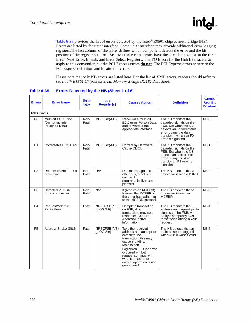
328 Intel® E8501 Chipset North Bridge (NB) Datasheet
Functional Description
Table 6-39 provides the list of errors detected by the Intel® E8501 chipset north bridge (NB). Errors are listed by the unit / interface. Some unit / interface may provide additional error logging registers.The last column of the table, defines which component detects the error and the bit position of the register set. For FSB, IMI and NB the errors have the same bit position in the First Error, Next Error, Emask, and Error Select Registers. The I/O Errors for the Hub Interface also apply to this convention but the PCI Express errors do not. The PCI Express errors adhere to the PCI Express definition and location of errors.
Please note that only NB errors are listed here. For the list of XMB errors, readers should refer to the Intel® E8501 Chipset eXternal Memory Bridge (XMB) Datasheet.
Table 6-39. Errors Detected by the NB (Sheet 1 of 6)
Error# Error Name Errortype
Log Register(s) Cause / Action Definition
Comp. Reg. Bit Position
FSB Errors
F0 Multi-bit ECC Error (Do not Include Poisoned Data)
Non-Fatal
RECFSB{A/B} Received a multi-bit ECC error. Poison Data and forward to the appropriate interface.
The NB monitors the data/dep signals on the FSB. Set when the NB detects an uncorrectable error during the data transfer in which an F0 error is signalled.
NB-0
F1 Correctable ECC Error Non-Fatal
RECFSB{A/B} Correct by Hardware, Cause CMCI.
The NB monitors the data/dep signals on the FSB. Set when the NB detects an correctable error during the data transfer an F1 error is signalled.
NB-1
F2 Detected BINIT from a processor
Non-Fatal
N/A Do not propagate to other bus, reset arb. unit, and programatically reset platform.
The NB detected that a processor issued a B-INIT.
NB-2
F3 Detected MCERR from a processor
Non-Fatal
N/A If (receive an MCERR) forward the MCERR to the other bus, adhering to the MCERR protocol.
The NB detected that a processor issued an MCERR.
NB-3
F4 Request/Address Parity Error
Fatal NRECFSB{A/B}_LOG[2:0]
Complete transaction on FSB, drop transaction, provide a response. Capture Address/Control information.
The NB monitors the address and request parity signals on the FSB. A parity discrepancy over these fields during a valid request.
NB-4
F5 Address Strobe Glitch Fatal NRECFSB{A/B}_LOG[2:0]
Take the received address and attempt to complete the transaction, this may cause the NB to Malfunction.Log which FSB the error occurred on. Let request continue with what it decodes to, correct operation is not guaranteed.
The NB detects that an address strobe toggled when ADS# wasn’t valid.
NB-5
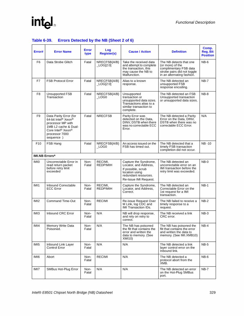
Intel® E8501 Chipset North Bridge (NB) Datasheet 329
Functional Description
F6 Data Strobe Glitch Fatal NRECFSB{A/B}_LOG[2:0]
Take the received data and attempt to complete the transaction, this may cause the NB to Malfunction.
The NB detects that one (or more) of the complimentary FSB data strobe pairs did not toggle in an alternating fashion.
NB-6
F7 FSB Protocol Error Fatal NRECFSB{A/B}_LOG[2:0]
Alias to a known response.
The NB detected an unsupported FSB response encoding.
NB-7
F8 Unsupported FSB Transaction
Fatal NRECFSB{A/B}_LOG0
Unsupported transaction or unsupported data sizes. Transactions alias to a similar transaction to complete.
The NB detected an FSB Unsupported transaction or unsupported data sizes.
NB-8
F9 Data Parity Error (for 64-bit Intel® Xeon®
processor MP with 1MB L2 cache & Dual-Core Intel® Xeon®
processor 7000 sequence )
Fatal NRECFSB Parity Error was detected on the Data, DINV, DSTB when there was no correctable ECC Error.
The NB detected a Parity Error on the Data, DINV, DSTB when there was no correctable ECC Error.
N/A
F10 FSB Hang Fatal NRECFSB{A/B}_LOG0
An access issued on the FSB has timed out.
The NB detected that a timely FSB transaction completion did not occur.
NB -10
IMI.NB Errorsa
IMI0 Uncorrectable Error in read return packet before retry limit exceeded
Non-Fatal
RECIMI, REDPIMIH
Capture the Syndrome, Locator, and Address, If possible, scrub location using redundant resources.Re-Issue IMI Request.
The NB detected an uncorrectable error on an IMI transaction before the retry limit was exceeded.
NB-0
IMI1 Inbound Correctable ECC Error
Non-Fatal
RECIMI, REDPIMIH
Capture the Syndrome, Locator, and Address, Correct.
The NB detected an Correctable Error on the 1st request for a IMI transaction.
NB-1
IMI2 Command Time-Out Non-Fatal
RECIMI Re-issue Request Over M Link, log CDC and IMI Transaction IDs.
The NB failed to receive a timely response to a request.
NB-2
IMI3 Inbound CRC Error Non-Fatal
N/A NB will drop response, and rely on retry to correct.
The NB received a link CRC error.
NB-3
IMI4 Memory Write Data Poisoned.
Non-Fatal
N/A The NB has poisoned the flit that contains the error and written the data to memory. (See XMI10)
The NB has poisoned the flit that contains the error and written the data to memory. (See IMI.XMB10)
NB-4
IMI5 Inbound Link Layer Control Error
Non-Fatal
N/A N/A The NB detected a link layer control error on the Inbound link.
NB-5
IMI6 Abort Non-Fatal
RECIMI N/A The NB detected a protocol abort from the XMB.
NB-6
IMI7 SMBus Hot-Plug Error Non-Fatal
N/A N/A The NB detected an error on the Hot-Plug SMBus port.
NB-7
Table 6-39. Errors Detected by the NB (Sheet 2 of 6)
Error# Error Name Error type
Log Register(s) Cause / Action Definition
Comp. Reg. Bit Position
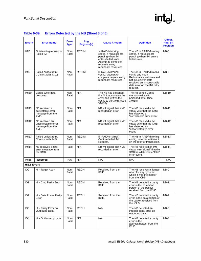
330 Intel® E8501 Chipset North Bridge (NB) Datasheet
Functional Description
IMI8 Outstanding request to Failed IMI
Non-Fatal
RECIMI In RAID/Mirroring config, if requests are pending when IMI enters failed state. Attempt to complete requests using redundant resources.
The NB in RAID/Mirroring config, if requests are pending when IMI enters failed state.
NB-8
IMI9 Failed on last retry. Co-exist with IMI13
Non-Fatal
RECIMI In RAID/Mirroring config, attempt to complete request using redundant resources.
The NB in RAID/Mirroring config and not in Redundancy lost state and not in Resilver state received an uncorrectable data error on the IMI retry request.
NB-9
IMI10 Config write data poisoned.
Non-Fatal
N/A The NB has poisoned the flit that contains the error and written the config to the XMB. (See XMI18).
The NB sent a Config memory write with poisoned data. (See XMI18)
NB-10
IMI11 NB received a correctable error message from the XMB
Non-Fatal
N/A NB will signal that XMB recorded an error.
The NB received a IMI virtual wire that the XMB has detected a “correctable” error event.
NB-11
IMI12 NB received an uncorrectable error message from the XMB
Non-Fatal
N/A NB will signal that XMB recorded an error.
The NB received a IMI virtual wire that the XMB has detected an “uncorrectable” error event.
NB-12
IMI13 Failed on last retry. Co-exist with IMI9
Non-Fatal
RECIMI If (RAID or Mirror) Capture failed IMI Request.
The NB in RAID/Mirroring config, receives a timeout on the retry of transaction.
NB-13
IMI14 NB received a fatal error message from the XMB
Fatal N/A NB will signal that XMB recorded an error.
The NB received an IMI virtual wire “signal” that the XMB has detected a “fatal” error event.
NB-14
IMI15 Reserved N/A N/A N/A N/A N/A
HI1.5 Errors
IO0 HI - Target Abort Non-Fatal
RECHI Received from the ICH5.
The NB receives a Target-Abort for any cycle for which it was the master from the ICH5.
NB-0
IO1 HI - Cmd Parity Error Non-Fatal
RECHI Received from the ICH5.
The NB detected a parity error in the command portion of the packet received from the ICH5.
NB-1
IO2 HI - Data Phase Parity Error
Non-Fatal
RECHI Received from the ICH5.
The NB detected a parity error in the data portion of the packet received from the ICH5.
NB-2
IO3 HI - Parity Error on Outbound Data
Non-Fatal
RECHI N/A The NB detected an internal parity error on outbound data.
NB-3
IO4 HI - Outbound poison Non-Fatal
N/A N/A The NB detected a parity error in the address/header from the ICH5.
NB-4
Table 6-39. Errors Detected by the NB (Sheet 3 of 6)
Error# Error Name Errortype
Log Register(s) Cause / Action Definition
Comp. Reg. Bit Position
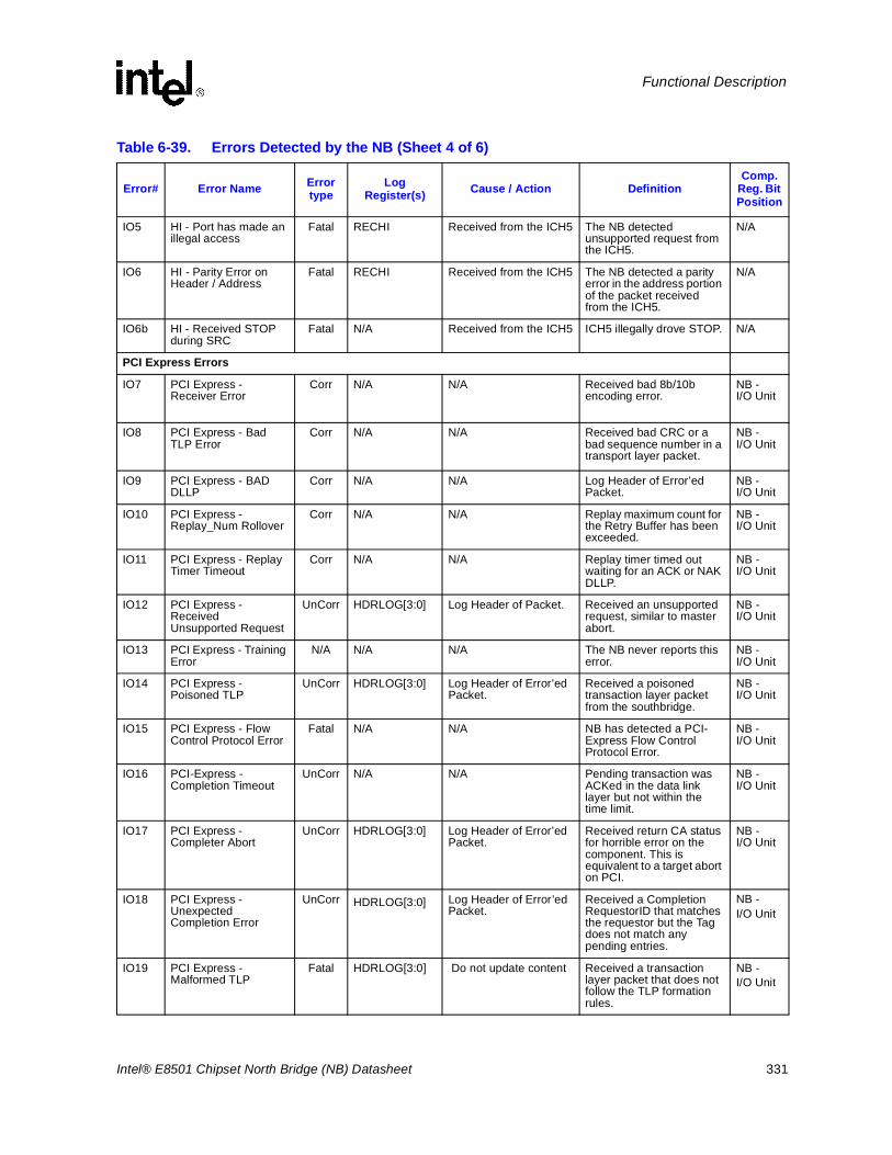
Intel® E8501 Chipset North Bridge (NB) Datasheet 331
Functional Description
IO5 HI - Port has made an illegal access
Fatal RECHI Received from the ICH5 The NB detected unsupported request from the ICH5.
N/A
IO6 HI - Parity Error on Header / Address
Fatal RECHI Received from the ICH5 The NB detected a parity error in the address portion of the packet received from the ICH5.
N/A
IO6b HI - Received STOP during SRC
Fatal N/A Received from the ICH5 ICH5 illegally drove STOP. N/A
PCI Express Errors
IO7 PCI Express - Receiver Error
Corr N/A N/A Received bad 8b/10b encoding error.
NB - I/O Unit
IO8 PCI Express - Bad TLP Error
Corr N/A N/A Received bad CRC or a bad sequence number in a transport layer packet.
NB - I/O Unit
IO9 PCI Express - BAD DLLP
Corr N/A N/A Log Header of Error’ed Packet.
NB - I/O Unit
IO10 PCI Express - Replay_Num Rollover
Corr N/A N/A Replay maximum count for the Retry Buffer has been exceeded.
NB -I/O Unit
IO11 PCI Express - Replay Timer Timeout
Corr N/A N/A Replay timer timed out waiting for an ACK or NAK DLLP.
NB -I/O Unit
IO12 PCI Express - ReceivedUnsupported Request
UnCorr HDRLOG[3:0] Log Header of Packet. Received an unsupported request, similar to master abort.
NB -I/O Unit
IO13 PCI Express - Training Error
N/A N/A N/A The NB never reports this error.
NB - I/O Unit
IO14 PCI Express - Poisoned TLP
UnCorr HDRLOG[3:0] Log Header of Error’ed Packet.
Received a poisoned transaction layer packet from the southbridge.
NB -I/O Unit
IO15 PCI Express - Flow Control Protocol Error
Fatal N/A N/A NB has detected a PCI-Express Flow Control Protocol Error.
NB - I/O Unit
IO16 PCI-Express - Completion Timeout
UnCorr N/A N/A Pending transaction was ACKed in the data link layer but not within the time limit.
NB -I/O Unit
IO17 PCI Express - Completer Abort
UnCorr HDRLOG[3:0] Log Header of Error’ed Packet.
Received return CA status for horrible error on the component. This is equivalent to a target abort on PCI.
NB -I/O Unit
IO18 PCI Express - UnexpectedCompletion Error
UnCorr HDRLOG[3:0] Log Header of Error’ed Packet.
Received a Completion RequestorID that matches the requestor but the Tag does not match any pending entries.
NB -I/O Unit
IO19 PCI Express -Malformed TLP
Fatal HDRLOG[3:0] Do not update content Received a transaction layer packet that does not follow the TLP formation rules.
NB -I/O Unit
Table 6-39. Errors Detected by the NB (Sheet 4 of 6)
Error# Error Name Error type
Log Register(s) Cause / Action Definition
Comp. Reg. Bit Position
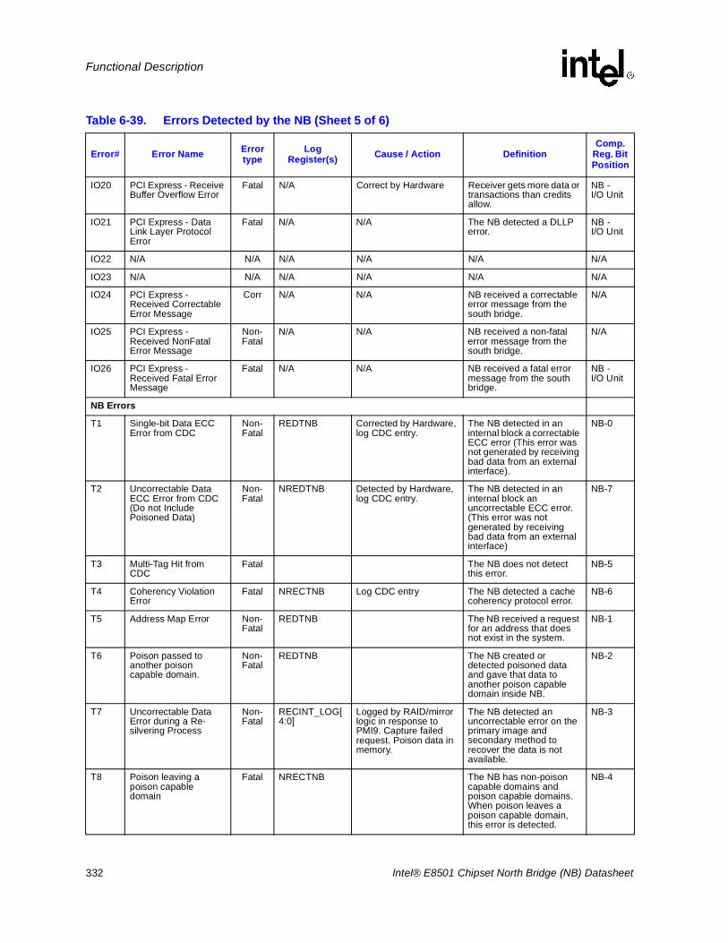
332 Intel® E8501 Chipset North Bridge (NB) Datasheet
Functional Description
IO20 PCI Express - Receive Buffer Overflow Error
Fatal N/A Correct by Hardware Receiver gets more data or transactions than credits allow.
NB -I/O Unit
IO21 PCI Express - Data Link Layer Protocol Error
Fatal N/A N/A The NB detected a DLLP error.
NB -I/O Unit
IO22 N/A N/A N/A N/A N/A N/A
IO23 N/A N/A N/A N/A N/A N/A
IO24 PCI Express - Received Correctable Error Message
Corr N/A N/A NB received a correctable error message from the south bridge.
N/A
IO25 PCI Express - Received NonFatal Error Message
Non-Fatal
N/A N/A NB received a non-fatal error message from the south bridge.
N/A
IO26 PCI Express - Received Fatal Error Message
Fatal N/A N/A NB received a fatal error message from the south bridge.
NB -I/O Unit
NB Errors
T1 Single-bit Data ECC Error from CDC
Non-Fatal
REDTNB Corrected by Hardware, log CDC entry.
The NB detected in an internal block a correctable ECC error (This error was not generated by receiving bad data from an external interface).
NB-0
T2 Uncorrectable Data ECC Error from CDC (Do not Include Poisoned Data)
Non-Fatal
NREDTNB Detected by Hardware, log CDC entry.
The NB detected in an internal block an uncorrectable ECC error. (This error was not generated by receiving bad data from an external interface)
NB-7
T3 Multi-Tag Hit from CDC
Fatal The NB does not detect this error.
NB-5
T4 Coherency Violation Error
Fatal NRECTNB Log CDC entry The NB detected a cache coherency protocol error.
NB-6
T5 Address Map Error Non-Fatal
REDTNB The NB received a request for an address that does not exist in the system.
NB-1
T6 Poison passed to another poison capable domain.
Non-Fatal
REDTNB The NB created or detected poisoned data and gave that data to another poison capable domain inside NB.
NB-2
T7 Uncorrectable Data Error during a Re-silvering Process
Non-Fatal
RECINT_LOG[4:0]
Logged by RAID/mirror logic in response to PMI9. Capture failed request. Poison data in memory.
The NB detected an uncorrectable error on the primary image and secondary method to recover the data is not available.
NB-3
T8 Poison leaving a poison capable domain
Fatal NRECTNB The NB has non-poison capable domains and poison capable domains. When poison leaves a poison capable domain, this error is detected.
NB-4
Table 6-39. Errors Detected by the NB (Sheet 5 of 6)
Error# Error Name Errortype
Log Register(s) Cause / Action Definition
Comp. Reg. Bit Position
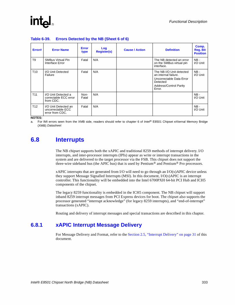
Intel® E8501 Chipset North Bridge (NB) Datasheet 333
Functional Description
6.8 InterruptsThe NB chipset supports both the xAPIC and traditional 8259 methods of interrupt delivery. I/O interrupts, and inter-processor interrupts (IPIs) appear as write or interrupt transactions in the system and are delivered to the target processor via the FSB. This chipset does not support the three-wire sideband bus (the APIC bus) that is used by Pentium® and Pentium® Pro processors.
xAPIC interrupts that are generated from I/O will need to go through an I/O(x)APIC device unless they support Message Signalled Interrupts (MSI). In this document, I/O(x)APIC is an interrupt controller. This functionality will be embedded into the Intel 6700PXH 64-bit PCI Hub and ICH5 components of the chipset.
The legacy 8259 functionality is embedded in the ICH5 component. The NB chipset will support inband 8259 interrupt messages from PCI Express devices for boot. The chipset also supports the processor generated “interrupt acknowledge” (for legacy 8259 interrupts), and “end-of-interrupt” transactions (xAPIC).
Routing and delivery of interrupt messages and special transactions are described in this chapter.
6.8.1 xAPIC Interrupt Message DeliveryFor Message Delivery and Format, refer to the Section 2.5, “Interrupt Delivery” on page 31 of this document.
T9 SMBus Virtual Pin Interface Error
Fatal N/A The NB detected an error on the SMBus virtual pin interface.
NB -I/O Unit
T10 I/O Unit Detected Failure
Fatal N/A The NB I/O Unit detected an internal failure.Uncorrectable Data Error DetectedAddress/Control Parity Error.
NB -I/O Unit
T11 I/O Unit Detected a correctable ECC error from CDC.
Non-Fatal
N/A NB - I/O Unit
T12 I/O Unit Detected an uncorrectable ECC error from CDC.
Fatal N/A NB - I/O Unit
NOTES:a. For IMI errors seen from the XMB side, readers should refer to chapter 6 of Intel® E8501 Chipset eXternal Memory Bridge
(XMB) Datasheet
Table 6-39. Errors Detected by the NB (Sheet 6 of 6)
Error# Error Name Error type
Log Register(s) Cause / Action Definition
Comp. Reg. Bit Position
334 Intel® E8501 Chipset North Bridge (NB) Datasheet
Functional Description
6.8.2 xAPIC Destination ModesThe destination mode refers to how the processor interprets the destination field of the interrupt message. There are two types of destination modes:
1. Physical Destination Mode2. Logical Destination Mode
The destination mode is selected by A[2] in PCI Express and Ab[5] on the FSB.
6.8.2.1 Physical Destination Mode (xAPIC)
In physical mode, the APIC ID is 8 bits, supporting up to 255 agents. Each processor has a Local APIC ID Register where the lower 5 bits are initialized by hardware (Cluster ID=ID[4:3], Bus Agent ID=ID[2:1], thread ID=ID[0]). The upper 3 bits default to 0s at system reset. These values can be modified by software. The Cluster ID is set by address bits A[12:11] during reset. By default, the NB will drive A[12:11] to ‘00’ for Front Side Bus A, and ‘01’ for Front Side Bus B. The value driven on bit A[12] during reset can be modified through the POC register on the NB.
The NB will not rely on the cluster ID or any other fields in the APIC ID to route interrupts. The NB will ensure the interrupt is seen on both busses and the processor with the matching APIC ID will claim the interrupt.
Physical destination mode interrupts can be directed, broadcast, or redirected. An xAPIC message with a destination field of all 1s denotes a broadcast to all.
In a directed physical mode message the agent claims the interrupt if the upper 8 bits of the destination field (DID field) matches the Local APIC ID of the processor or the interrupt is a broadcast interrupt.
6.8.2.2 Logical Destination Mode (xAPIC)
In logical destination mode, destinations are specified using an 8-bit logical ID field. Each processor contains a register called the Logical Destination Register (LDR) that holds this 8-bit logical ID. Interpretation of the LDR is determined by the contents of the processor’s Destination Format Register (DFR). The DFR establishes if the processor is in flat or cluster mode. Logical destination mode interrupts can be directed (fixed delivery), redirectable (lowest priority delivery), or broadcast. The LDR is initialized to flat mode (0) at reset and is programmed by firmware (and can be changed by system software). The NB also has an equivalent bit in the XTPR0 register to indicate flat or cluster mode.
Interpretation of the destination field of the xAPIC message and the logical ID of the processor is different whether the processor is in flat or cluster mode. The 2 models are flat and cluster:
Flat Model - The 8-bit logical ID is compared to the 8-bit destination field of the incoming interrupt message. If there is a bit-wise match, then the local xAPIC is selected as a destination of the interrupt. Each bit position in the destination field corresponds to an individual Local xAPIC Unit. The flat model supports up to 4 agents in the system. An xAPIC message where the DID (destination field) is all 1’s is a broadcast interrupt.Cluster Model - The 8-bit logical ID is divided into two fields, where the upper four bits contain a cluster ID, and the lower 4-bits identifies the agent within the cluster using the same encoding scheme as the flat model. Up to 8 logical clusters (2 agents each) can be supported. An xAPIC message where the lower 4-bits of the DID is all 1’s is a broadcast interrupt within a cluster. Interrupt redirection can only be applied to processors within the cluster.
Intel® E8501 Chipset North Bridge (NB) Datasheet 335
Functional Description
Interrupt messages that originate from I/O(x)APIC devices or from processing nodes must be routed and delivered to the target agents in the system. In general xAPIC messages are delivered to both FSB’s because there is no reliable way to determine the destination node of the message for the destination field. Interrupts originating from I/O can be generated from a PCI agent using MSI interrupts, or by an interrupt controller on a bridge chip such as the Intel 6700PXH 64-bit PCI Hub or ICH5. Table 6-40 shows the routing rules used for routing xAPIC messages in a NB platform. This table is valid for both broadcast and non-broadcast interrupts.
6.8.3 EOIFor Intel® Xeon® Processor Family (XPF) platforms using xAPIC, the EOI is a specially encoded FSB transaction with the interrupt vector attached. Since the EOI is not directed, the NB will broadcast the EOI transaction to all I/O(x)APICs.
Note: Since the ICH5 does not support the EOI special cycle, the Intel® E8501 chipset will translate the EOI into a directed write to the EOI register in the ICH5.
6.8.4 I/O InterruptsFor I/O interrupts from the Intel 6700PXH 64-bit PCI Hub and ICH5 components receive interrupts with either dedicated interrupt pins or with writes to the integrated redirection table. The I/OxAPIC controller integrated within these components turns these interrupts into writes destined for the FSB with a specific address.
Interrupts triggered from an I/O device can be triggered with either a dedicated interrupt pin or through an inbound write message from the PCI bus (MSI). Note that if the interrupt is triggered by a dedicated pin, the I/OxAPIC controller in the I/O bridge (Intel 6700PXH 64-bit PCI Hub or ICH5) turns this into an inbound write. On the FSB, the interrupt is converted to an interrupt request. Other than a special interrupt encoding, the FSB interrupt follows the same format as discussed in Section 2.5, “Interrupt Delivery” on page 31. Therefore, to all components other than the Intel 6700PXH 64-bit PCI Hub, ICH5, and the processors, an interrupt is an inbound write following the format mentioned in Section 2.5, the NB will not write combine or cache the APIC address space.
I/O(x)APICs can be configured through two mechanisms. The traditional mechanism is the hard coded FEC0_0000h to FECF_FFFFh range is used to communicate with the IOAPIC controllers in the Intel 6700PXH 64-bit PCI Hub or ICH5.
The second method is to use the standard MMIO range to communicate to the Intel 6700PXH 64-bit PCI Hub. To accomplish this, the PXH.MBAR must be programmed within the PCI Express device MMIO region.
Table 6-40. NB xAPIC Interrupt Message Routing and Delivery
Source Type Routing
I/O physical or logical directed Deliver to both FSB’s as an interrupt transaction.
Processor physical or logical directed Deliver to other FSB as an interrupt transaction.
Any Sourcelogical, redirectablephysical, redirectable
Redirection is performed by the NB and is delivered to both front side buses.
336 Intel® E8501 Chipset North Bridge (NB) Datasheet
Functional Description
6.8.5 OrderingHandling interrupts as inbound writes has inherent advantages. First, there is no need for the additional APIC bus resulting in extra pins and board routing concerns. Second, with an out-of-band APIC bus, there are ordering concerns. Any interrupt needs to be ordered correctly and all prior inbound writes must get flushed ahead of the interrupt. The PCI Local Bus Specification,Revision 2.2 attempts to address this by requiring all interrupt routines to first read the PCI interrupt register. Since PCI read completions are required to push all writes ahead of it, then all writes prior to the interrupt are guaranteed to be flushed. This, However assumes that all drivers perform this read.
6.8.6 Hardware IRQ IOxAPIC InterruptsDedicated pin interrupts may be edge or level-triggered. They are routed to IRQ pins on IOxAPIC device such as the Intel 6700PXH 64-bit PCI Hub and ICH5. The IOxAPIC device will convert the interrupt into either an xAPIC or 8259 interrupt.
For level-triggered interrupts, the I/OxAPIC will generate an interrupt message when any of the interrupt lines coming into it become asserted. The processor will handle the interrupt and eventually write to the initiating device that the interrupt is complete. The device will de-assert the interrupt line to the I/OxAPIC. After the interrupt has been serviced, the processor sends an EOI command to inform the I/OxAPIC that the interrupt has been serviced. Since the EOI is not directed, the NB will broadcast the EOI transaction to all I/O(x)APIC’s. If the original I/O(x)APIC sees the interrupt is still asserted, it knows there’s another interrupt (shared interrupts) and will send another interrupt message.
For edge-triggered interrupts, the flow is the same except that there is no EOI message indicating that the interrupt is complete. Since the interrupt is issued whenever an edge is detected, EOIs are not necessary.
While not recommended, agents can share interrupts to better utilize each interrupt (implying level-triggered interrupts). Due to ordering constraints, agents can not use an interrupt controller that resides on a different PCI bus. Therefore only agents on the same PCI bus can share interrupts (or the driver MUST follow the PCI requirement that interrupt routines must first read the PCI interrupt register).
The NB supports the INTA (interrupt acknowledge) special bus cycle for legacy 8259 support. These are routed to the compatibility ICH5 in the system. The INTA will return data that provides the interrupt vector.
6.8.7 Message Signalled Interrupts (MSI)A second mechanism for devices to send interrupts is to issue the Message Signalled Interrupt (MSI) introduced in the PCI Local Bus Specification, Revision 2.2 . This appears as a 1 DWORD write on the PCI/PCI-X/PCI Express bus.
With PCI devices, there are 2 types of MSIs. One type is where a PCI device issues the inbound write to the interrupt range. The other type of MSI is where a PCI device issues an inbound write to the upstream APIC controller (for example, in the Intel 6700PXH 64-bit PCI Hub) where the APIC controller converts it into an inbound write to the interrupt range. The second type of MSI can be used in the event the OS doesn’t support MSIs, but the BIOS does. For either way, the interrupt will appear as an inbound write to the NB over the PCI Express ports.
Intel® E8501 Chipset North Bridge (NB) Datasheet 337
Functional Description
MSI is expected to be supported by the operating systems about the same time frame as Intel®E8501 chipset availability. A NB chipset-based platform will also feature a backup interrupt mechanism in the event that there is a short period of time when MSI is not available. This is described in the next section.
6.8.8 Non-MSI Interrupts - “Fake MSI”For interrupts coming through the Intel 6700PXH 64-bit PCI Hub or ICH5 components, their APIC controller will convert interrupts into inbound writes, so inbound interrupts will appear in the same format as an MSI.
For interrupts that are not coming through an APIC controller (for example Dual Northway, a dual port 1 GbE) it is still required that the interrupt appear as an MSI-like interrupt. If the OS does not yet support MSI, the PCI Express device can be programmed by the BIOS to issue inbound MSI interrupts to an IOxAPIC in the system. The safest IOxAPIC to choose would be the ICH5 since it is always present in a system. The NB does not support the PCI Express “Assert_Int” and “Deassert_Int” packets for xAPIC interrupts.
In this method, PCI Express devices are programmed to enable MSI functionality, and given a write path directly to the pin assertion register in a selected IOxAPIC already present in the platform. The IOxAPIC will generate an interrupt message in response, thus providing equivalent functionality to a virtual (edge-triggered) wire between the PCI Express endpoint and the I/OxAPIC.
All PCI Express devices are strictly required to support MSI. When MSI is enabled, PCI Express devices generate a memory transaction with an address equal to the I/OxAPIC_MEM_BAR + 20 and a 32-bit data equal to the interrupt vector number corresponding to the device. This information is stored in the device's MSI address and data registers, and would be initialized by the system firmware (BIOS) prior to booting a non-MSI aware operating system (With the theory that an MSI aware O/S would then over-write the registers to provide interrupt message delivery directly from the endpoint to the CPU complex).
The PCI Express memory write transaction propagates to the NB and is redirected down the appropriate PCI Express port following the NB IOAPIC address mapping definition. The IOAPIC memory space ranges are fixed and cannot be relocated by the OS. The assert message is indistinguishable from a memory write transaction, and is forwarded to the destination I/OxAPIC (which will then create an upstream APIC interrupt message in the form of an inbound memory write). The write nature of the message “pushes” all applicable pre-interrupt traffic through to the NB core, and the NB core architecture guarantees that the subsequent APIC message cannot pass any posted data already within the NB.
6.8.9 Inter Processor Interrupts (IPIs)The IPIs will be covered in the future revision of this document.
338 Intel® E8501 Chipset North Bridge (NB) Datasheet
Functional Description
6.8.10 Chipset Generated InterruptsThe Intel® E8501 chipset can trigger interrupts for chipset errors and for PCI Express and IMI Port Hot-Plug. For these events, the chipset can be programmed to assert pins that the system can route to an APIC controller. The following is a preliminary list of interrupts that can be generated:
1. Chipset Error: Chipset asserts appropriate ERR pin, depending on severity. This can be routed by the system to generate an interrupt at an interrupt controller. (NB pins ERR[2:0], MCERR, ICH Reset). For details on Chipset error types and reporting, please see Section 6.7.1.
2. IMI Hot-Plug: Chipset asserts IMI_HPINT on behalf of an IMI Hot-Plug event. This can be routed by the system to generate an interrupt. This document assumes that IMI_HPINT will be connected either to a system interrupt, SMI interrupt, or SCI (ACPI) general purpose event.
3. PCI Express Error:
Chipset asserts appropriate ERR pin, depending on severity. This can be routed by the system to generate an interrupt.
• The NB can receive error indications from the PCI Express ports. These are in the form of inbound ERR_COR/UNC/FATAL messages. The NB will assert the appropriate ERR signal just like any internal NB error.
4. PCI Express Hot-Plug:
The NB asserts EXP_HPINT on behalf of a PCI Express Hot-Plug event.
• NB generated Hot-Plug event such as PresDet change, Attn button, MRL sensor changed, power fault, etc. Each of these events has a corresponding bit in the PCI Express Hot-Plug registers (Attention Button, Power Indicator, Power Controller, Presence Detect, MRL Sensor, Port Capabilities/Slot registers). This will generate an interrupt via the EXP_HPINT pin, or it will generate an MSI.
— EXP_HPINT: When software has completed servicing the Hot-Plug event, it will clear the appropriate bit in the PCI Express Hot-Plug register(s), at which point, the NB can deassert EXP_HPINT.
— MSI: If the MSICTRL.MSIEN bit (MSI enabled) is set, the NB will generate an MSI in response to a PCI Express Hot-Plug event. More details will be added in the subsequent revision of this document.
Intel® E8501 Chipset North Bridge (NB) Datasheet 339
Functional Description
Table 6-41 summarizes the different types of chipset generated interrupts that were discussed. Although the interrupt and SW mechanism is flexible and can be changed depending on how the system is hooked up, for reference this table also describes what SW mechanism is expected to be used.
• PCI Express Hot-Plug event from downstream. This could be either an MSI or a GPE message.
— MSI: Handled like a normal MSI interrupt.
— GPE Message: Upon receipt of a Assert_GPE message from PCI Express, NB will assert the EXP_HPINT signal to generate this interrupt. To generate an SCI (ACPI), this signal will be routed to the ICH5 appropriate GPIO pin to match the GPE0_EN register settings. When the Hot-Plug event has been serviced, the NB will receive a Deassert_GPE message. At this point the NB can deassert EXP_HPINT. There needs to be a tracking bit per PCI Express port to keep track of Assert/Deassert_GPE pairs. These tracking bits should be ORed together to determine whether to drive the EXP_HPINTpin. If one or more of the tracking bits are set (meaning we have received one or more Assert_GPE messages), EXP_HPINT must be set until all the matching Deassert_GPE messages are received.
— Sideband Signals: Some systems may choose to connect the interrupt via sideband signals directly to the ICH5. No action is required from the NB.
5. PCI Express PM: The NB asserts PME_OUT pin when a power management event is detected. PCI Express sends a PME message.
• Upon receipt of the PME message, the NB will assert the PME_OUT signal to generate this interrupt if enabled through bit 3 in ‘EXP_RTCTRL[7:1]: PCI Express Root Control Register (D1-7, F0)”. To generate an SCI (ACPI), this signal will be routed to the ICH5 appropriate GPIO pin to match the GPE0_EN settings. When software has completed servicing the power management event, it will clear the PCI Express RTSTS.PMESTS bit (by writing 1), at which point the NB can deassert PME_OUT.
6. PCI Hot-Plug: The NB will receive an Assert/Deassert GPE message from the PCI Express port when a PCI Hot-Plug event is happening. Assert/Deassert GPE messages should be treated the same as Assert/Deassert GPE messages for PCI Express Hot-Plug. (Keep track of Assert/Deassert GPE messages from each port and assert EXP_HPINT appropriately).
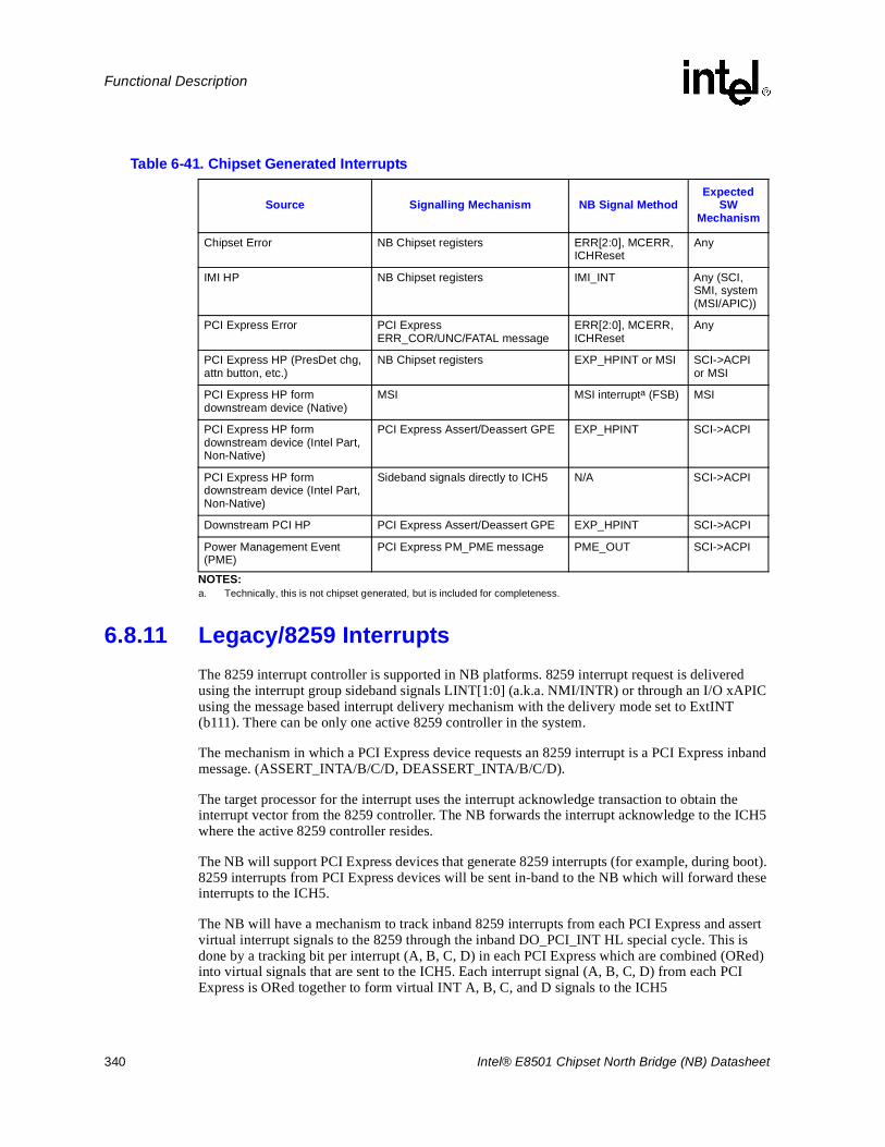
340 Intel® E8501 Chipset North Bridge (NB) Datasheet
Functional Description
6.8.11 Legacy/8259 InterruptsThe 8259 interrupt controller is supported in NB platforms. 8259 interrupt request is delivered using the interrupt group sideband signals LINT[1:0] (a.k.a. NMI/INTR) or through an I/O xAPIC using the message based interrupt delivery mechanism with the delivery mode set to ExtINT (b111). There can be only one active 8259 controller in the system.
The mechanism in which a PCI Express device requests an 8259 interrupt is a PCI Express inband message. (ASSERT_INTA/B/C/D, DEASSERT_INTA/B/C/D).
The target processor for the interrupt uses the interrupt acknowledge transaction to obtain the interrupt vector from the 8259 controller. The NB forwards the interrupt acknowledge to the ICH5 where the active 8259 controller resides.
The NB will support PCI Express devices that generate 8259 interrupts (for example, during boot). 8259 interrupts from PCI Express devices will be sent in-band to the NB which will forward these interrupts to the ICH5.
The NB will have a mechanism to track inband 8259 interrupts from each PCI Express and assert virtual interrupt signals to the 8259 through the inband DO_PCI_INT HL special cycle. This is done by a tracking bit per interrupt (A, B, C, D) in each PCI Express which are combined (ORed) into virtual signals that are sent to the ICH5. Each interrupt signal (A, B, C, D) from each PCI Express is ORed together to form virtual INT A, B, C, and D signals to the ICH5
Table 6-41. Chipset Generated Interrupts
Source Signalling Mechanism NB Signal MethodExpected
SWMechanism
Chipset Error NB Chipset registers ERR[2:0], MCERR, ICHReset
Any
IMI HP NB Chipset registers IMI_INT Any (SCI, SMI, system (MSI/APIC))
PCI Express Error PCI Express ERR_COR/UNC/FATAL message
ERR[2:0], MCERR, ICHReset
Any
PCI Express HP (PresDet chg, attn button, etc.)
NB Chipset registers EXP_HPINT or MSI SCI->ACPI or MSI
PCI Express HP form downstream device (Native)
MSI MSI interrupta (FSB)
NOTES:a. Technically, this is not chipset generated, but is included for completeness.
MSI
PCI Express HP form downstream device (Intel Part, Non-Native)
PCI Express Assert/Deassert GPE EXP_HPINT SCI->ACPI
PCI Express HP form downstream device (Intel Part, Non-Native)
Sideband signals directly to ICH5 N/A SCI->ACPI
Downstream PCI HP PCI Express Assert/Deassert GPE EXP_HPINT SCI->ACPI
Power Management Event (PME)
PCI Express PM_PME message PME_OUT SCI->ACPI
Intel® E8501 Chipset North Bridge (NB) Datasheet 341
Functional Description
(DO_PCI_INTA/B/C/D (assertion encoding)). When all the tracking bits for a given interrupt (A, B, C, or D) are cleared from all PCI Express ports, the virtual signal A, B, C, or D is deasserted via the inband DO_PCI_INT (deassertion encoding).
For PCI Express hierarchies, interrupts will be consolidated at each level. For example, a PCI Express switch connected to a NB PCI Express port will only send a maximum of 4 interrupts at a time, regardless of how many interrupts are issued downstream.
SMI (System Management Interrupt) interrupts are initiated by the SMI# signal in the platform. On accepting a System Management Interrupt, the processor saves the current state and enters SMM.
6.9 Reset
6.9.1 IntroductionThis section describes NB-specific aspects of hardware reset. Subsequent I/O initialization procedures requiring configuration register dialogue are not covered in this section.
NB expects to receive RSTIN# from the ICH5 chip. NB uses this signal to reset the internal state of NB, and additionally, forwards this reset to the processor(s) in the system via the H_A_RST# and H_B_RST# signals. NB controls the reset of the XMB chips connected to NB via software using the IMI_{A/B/C/D}_RST# signals which are expected to be connected from NB to XMB.
A system is expected to connect the ICHRST# pin of NB to the PLD controlling the system reset logic that generates the PCIRST# signal into the ICH5 chip.
NB will keep H_{A/B}_RST# asserted on an FSB which indicates no end agent is present via the H_{A/B}_PRSNT# pin; the system should keep the core and cache VR disabled in this case to avoid any CPU thermal issues.
6.9.2 Types of Reset• Power-up
• Power Good
• PWROKThe PWROK reset spawns a hard reset.
• HardThe hard reset spawns IMI, PCI Express, and Processor resets.
• IMI
• Warm
• PCI Express
• JTAG
• SMBus
342 Intel® E8501 Chipset North Bridge (NB) Datasheet
Functional Description
6.9.3 Triggers of Reset• Energize power supplies
• PWRGOOD de-assertion
• RESTIN# assertion
• NB.SYRE.SYSRST (refer to Section 4.14.8)
• IMI.ICHRST_inband_signal
• NB.SYRE.ROR (refer to Section 4.14.8)
• NB.IMIHPC.NEXTSTATE change (Refer to Section 4.13.10)IMI initialization time-out is covered by STATE change.
• NB.BCTRL.SRESET (Refer to Section 4.11.27)
• SMBus protocol
6.9.4 Trigger to Type AssociationThis section describes which triggers initiate which types:
• Energize power supplies: Power-up
• PWRGOOD de-assertion: Power good
• RESTIN# assertion: Hard
• NB.SYRE.ROR: Warm
• NB.IMIHPC.NEXTSTATE set to “Reset” or “RecoveryReset”: IMI
• NB.BCTRL.SRESET: PCI Express
• TRST# assertion or TCK/TMS protocol: JTAG
• SMBus protocol: SMBus
6.9.5 Logic Domain BehaviorDuring reset, each of the logic domains is treated as follows:
• Unaffected by reset:
— PLL’s
• Indirectly affected by reset:
— ArraysInitialized by BIST engines
— Analog I/O compensationOnly triggered by power-up
• {Boundary scan chains, JTAG protocol engine}:
— Asynchronous PWRGOOD de-assertion, PWRGOOD de-asserted, asynchronous TRST# assertion, ITP_TRST# asserted, or synchronous TCK/TMS protocol navigation to reset state: Reset
Intel® E8501 Chipset North Bridge (NB) Datasheet 343
Functional Description
• SMBus protocol engine:
— Asynchronous PWRGOOD de-assertion, PWRGOOD de-asserted, or synchronous SMBus reset protocol: Reset
• Sticky configuration bits:Configuration bits with the “ST” attribute are sticky
— Asynchronous PWRGOOD de-assertion, PWRGOOD de-asserted: Defaults
— (Synchronized RESTIN# assertion or synchronized RESTIN# asserted) while PWRGOOD asserted: No-ChangeSticky configuration bits must be protected from spurious activity at RESTIN# transitions and while RESTIN# is asserted during hard reset.
• IMI (NB):
— Asynchronous PWRGOOD de-assertion, PWRGOOD de-asserted, one cycle after synchronized RESTIN# assertion, IMISC.STATE set to “Reset” or “RecoveryReset” set: reset and tri-state outputs.
— Synchronized RESTIN# de-assertion, IMISC.STATE set to “Reset” or “RecoveryReset” cleared and synchronized RESTIN# de-asserted: Initialize then begin normal operation.
• RESTIN# pad:
— Synchronized through two HCLKIN-ed stagesThis is the synchronized RESTIN#.
• ICHRST# pad:
— asynchronous PWRGOOD de-assertion, PWRGOOD de-asserted: de-asserted
— ICHRST# cycle counter not extinguished: Asserted
• PCI Express:
— Asynchronous PWRGOOD de-assertion, PWRGOOD de-asserted: Tri-state and Reset
— PWRGOOD asserted, one cycle after synchronized RESTIN# assertion, BCTRL.SRESET set: link down
— RESTIN# de-assertion, BCTRL.SRESET cleared: initialize, train, link up
• IMI_{A/B/C/D}_RST# pad:
— Controlled by BIOS
— Asynchronous PWRGOOD de-assertion, PWRGOOD de-asserted, one cycle after synchronized RESTIN# assertion, IMISC.STATE set to “Reset” or “RecoveryReset” set: Asserted
— Synchronized RESTIN# de-assertion, IMISC.STATE set to “Reset” or “RecoveryReset” cleared and synchronized RESTIN# de-asserted: De-asserted.
• H_{A/B}_RST# pad:
— Asynchronous PWRGOOD de-assertion, PWRGOOD de-asserted, one cycle after synchronized RESTIN# assertion, SYRE.ROR asserted and bus locks cleared and IOQ’s flushed and data buffers flushed and IMI.REFRESH detected: assert
• SYRE.ROR configuration bit
— asynchronous PWRGOOD de-assertion, PWRGOOD de-asserted, one cycle after synchronized RESTIN# assertion, 1 HCLKIN after processor RESET# pad asserted: clear
344 Intel® E8501 Chipset North Bridge (NB) Datasheet
Functional Description
• Power-On Configuration:
— Minimum of 1 HCLKIN after processor RESET# pad asserted: Assert
— 2-19 HCLKIN after processor RESET# pad de-asserted: De-assert
• Hub Interface:
— Asynchronous PWRGOOD de-assertion, PWRGOOD de-asserted, one cycle after synchronized RESTIN# assertion: Reset and Tri-stated
— Synchronized RESTIN# de-asserted: Send NOP -> wait for NOP_ACK -> send CPU_RESET_DONE
6.9.6 PWRGOOD De-assertedTrigger = PWRGOOD de-assertion: Asynchronous
Power and master clocks remain stable.
• De-assert ICHRST# asynchronously.
• Assert H_{A/B}_RST# and IMI_{A/B/C/D}_RST# asynchronously.
• De-assert other front side bus I/O asynchronously.
• Tri-state other I/O.
• Toggle PLL outputs.
• Reset I/O Ports.
• Resolve multiple drivers to a non-destructive state.
6.9.7 PWRGOOD AssertionTrigger = PWRGOOD assertion: Synchronized
Voltages are within specifications. Master clocks are stable. The TCK signal may be in any state.
• Sample straps.
• Enable Power-On-Configuration (POC) to the front side bus.
• Un-tri-state I/O.
• Hold PCI Express link down.
6.9.8 NB ICHRST# SequenceTriggers = {H_{A/B}_RST#, ICHRST#, IMI_{A/B/C/D}_RST# Reset Signal and NB.SYRE.SYSRST Set}: Synchronous
• Assert ICHRST# for approximately 100 µs asynchronously to CLK66
• De-assert ICHRST# asynchronously to CLK66.This de-assertion must wait until 100 µs elapses, even though RESTIN# will be asserted before 100 µs elapses.
• Clear SYRE.SYSRST when ICHRST# is asserted.
Intel® E8501 Chipset North Bridge (NB) Datasheet 345
Functional Description
6.9.9 Hard Reset Asserted
Trigger = RESTIN# assertion: Synchronized
PWRGOOD is asserted.
• Protect sticky configuration bits.Sticky configuration bits must not log spurious errors resulting from the reset process. These processes include de-activated buses, initialization sequences, and spurious inputs on internal interfaces.
• Synchronously assert internal asynchronous flip-flop initialization inputs.Private JTAG chains may be reset.Exceptions: synchronous test-mode flip-flops, sticky configuration bits, JTAG controller and boundary-scan logic, and analog I/O compensation.
• Assert H_{A/B}_RST#.
• Do not assert IMI_{A/B/C/D}_RST# - software causes this to assert.
• Initialize non-PCI Express I/O port operation.
• Tri-state IMI I/O after 16 HCLKIN.
• Reset PCI Express protocol.
• Take PCI Express link down.
• Drive processor Power-On-Configuration (POC).POC is driven from the SYRE.CPUBIST, POC, and POC_AUX{A/B} configuration registers. The default values of these configuration registers do not require any processor request signals to be asserted when PWRGOOD is first asserted.
• De-assert non-POC front side bus signals.
6.9.10 Hard Reset De-assertionTrigger = RESTIN# de-assertion: synchronized
PWRGOOD is asserted.
• Allow normal operation of sticky configuration bits.
• Initiate physical IMI initialization.
• Initiate each remaining IMI initialization sequence: handshake, link-width negotiation, and deskew-and-frame.
• Send NOP message to Hub Interface. Wait for NOP_ACK reply from Hub Interface. Send CPU_RESET_DONE message to Hub Interface.
• Initialize PCI Express link.
• Engage PCI Express link training.
• Bring PCI Express link up.
• After approximately 1 ms, de-assert processor RESET#.
• After processor RESET# de-assertion + 2 HCLKIN, disable POC.
346 Intel® E8501 Chipset North Bridge (NB) Datasheet
Functional Description
6.9.11 PCI Express Reset AssertedTrigger = BCTRL.SRESET set: Synchronous
• Initialize PCI Express protocol.
• Take PCI Express link down.
6.9.12 NB PCI Express Reset De-assertedTrigger = BCTRL.SRESET cleared: synchronous
• Initialize PCI Express link.
• Engage PCI Express link training.
• Bring PCI Express link up.
6.9.13 NB IMI Reset AssertionTrigger = IMIHPC.NEXTSTATE set to “Reset” or “RecoveryReset”: synchronous
• Assert IMI_{A/B/C/D}_RST#.
• Tri-state IMI I/O (not including IMI_{A/B/C/D}_RST#).
6.9.14 NB IMI Reset De-assertionTrigger = IMIHPC.NEXTSTATE set to “Init” or “RecoveryInit”: Synchronous
• De-assert XMB IMI_RST#.
• IMI initiates physical initialization.
• After completion of IMI physical initialization, each IMI initiates each remaining initialization sequence: handshake, link-width negotiation, and deskew-and-frame.
6.9.15 Warm Reset SequenceTrigger = SYRE.ROR set or SYRE.CPURST set: Synchronous
• If SYRE.ROR is set, wait for an inband IMI.REFRESH signal from IMI designated by SYRE.REFPMI.
• Assert H_{A/B}_RST#.
6.9.15.1 Processor Reset Sequence
This is the entry point for a processor reset spawned by a “hard” reset. This is also a continuation of the warm reset sequence.
Trigger = Processor RESET# assertion: Synchronous
• After processor RESET# assertion + minimum of 1 HLCKIN, enable POC.POC is driven from the SYRE.CPUBIST, POC, and POC_AUX[1:0] configuration registers.
Intel® E8501 Chipset North Bridge (NB) Datasheet 347
Functional Description
• Logically mask front side bus inputs.
• Clear SYRE.ROR and SYRE.CPURST.
• After minimum of 1 ms, de-assert processor RESET#.
• After observing de-assertion of processor RESET#, resume front side bus protocol.
• After processor RESET# de-assertion + minimum of 2 HCLKIN, disable POC.
6.9.16 JTAG Reset AssertionTriggers = {TRST# assertion: asynchronous; TMS asserted for 5 TCK rising edges: Synchronous}
• Initialize JTAG finite-state-machine.
• Initialize boundary-scan chain.
6.9.17 JTAG Reset De-assertionTrigger = ITP_TRST# de-assertion: Asynchronous
• Release JTAG port and to operate normally.
• Release boundary-scan chain to operate normally.
6.9.18 SMBus Reset SequenceTrigger = SMBus protocol: Synchronous
• Reset SMBus interface
6.10 System ManagementThe NB chipset supports three methods of providing system management to the platform:
• Processor Access - All registers of the NB Chipset are available via a FSB access.
• SMBus Access - Via an SMBus access to the NB, a register access can be generated to the NB, any XMB, PCI Express device or ICH5. In addition, an SMBus access can go directly to the XMB. It should be noted that unlike processor accesses, the SMBus interface does have some restrictions, namely:
— SMBus cannot generate a Memory access at the NB or XMB
• JTAG Access - The same limitation and restrictions that apply to the SMBus interface also apply to the JTAG interface of the NB components.
The NB chipset provides a fully functional SMBus (or JTAG) target interface, which gives direct access to all internal chipset configuration registers. SMBus/JTAG access provides for a highly flexible platform management architecture when used in conjunction with a baseboard management controller (BMC) with an integrated network interface controller (NIC) function.
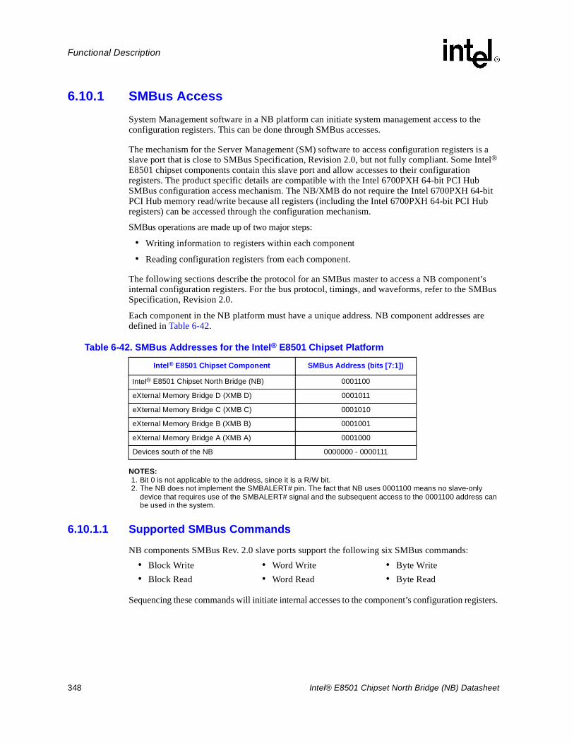
348 Intel® E8501 Chipset North Bridge (NB) Datasheet
Functional Description
6.10.1 SMBus AccessSystem Management software in a NB platform can initiate system management access to the configuration registers. This can be done through SMBus accesses.
The mechanism for the Server Management (SM) software to access configuration registers is a slave port that is close to SMBus Specification, Revision 2.0, but not fully compliant. Some Intel®E8501 chipset components contain this slave port and allow accesses to their configuration registers. The product specific details are compatible with the Intel 6700PXH 64-bit PCI Hub SMBus configuration access mechanism. The NB/XMB do not require the Intel 6700PXH 64-bit PCI Hub memory read/write because all registers (including the Intel 6700PXH 64-bit PCI Hub registers) can be accessed through the configuration mechanism.
SMBus operations are made up of two major steps:
• Writing information to registers within each component
• Reading configuration registers from each component.
The following sections describe the protocol for an SMBus master to access a NB component’s internal configuration registers. For the bus protocol, timings, and waveforms, refer to the SMBus Specification, Revision 2.0.
Each component in the NB platform must have a unique address. NB component addresses are defined in Table 6-42.
NOTES:1. Bit 0 is not applicable to the address, since it is a R/W bit.2. The NB does not implement the SMBALERT# pin. The fact that NB uses 0001100 means no slave-only
device that requires use of the SMBALERT# signal and the subsequent access to the 0001100 address can be used in the system.
6.10.1.1 Supported SMBus Commands
NB components SMBus Rev. 2.0 slave ports support the following six SMBus commands:
Sequencing these commands will initiate internal accesses to the component’s configuration registers.
Table 6-42. SMBus Addresses for the Intel® E8501 Chipset Platform
Intel® E8501 Chipset Component SMBus Address (bits [7:1])
Intel® E8501 Chipset North Bridge (NB) 0001100
eXternal Memory Bridge D (XMB D) 0001011
eXternal Memory Bridge C (XMB C) 0001010
eXternal Memory Bridge B (XMB B) 0001001
eXternal Memory Bridge A (XMB A) 0001000
Devices south of the NB 0000000 - 0000111
• Block Write • Word Write • Byte Write• Block Read • Word Read • Byte Read
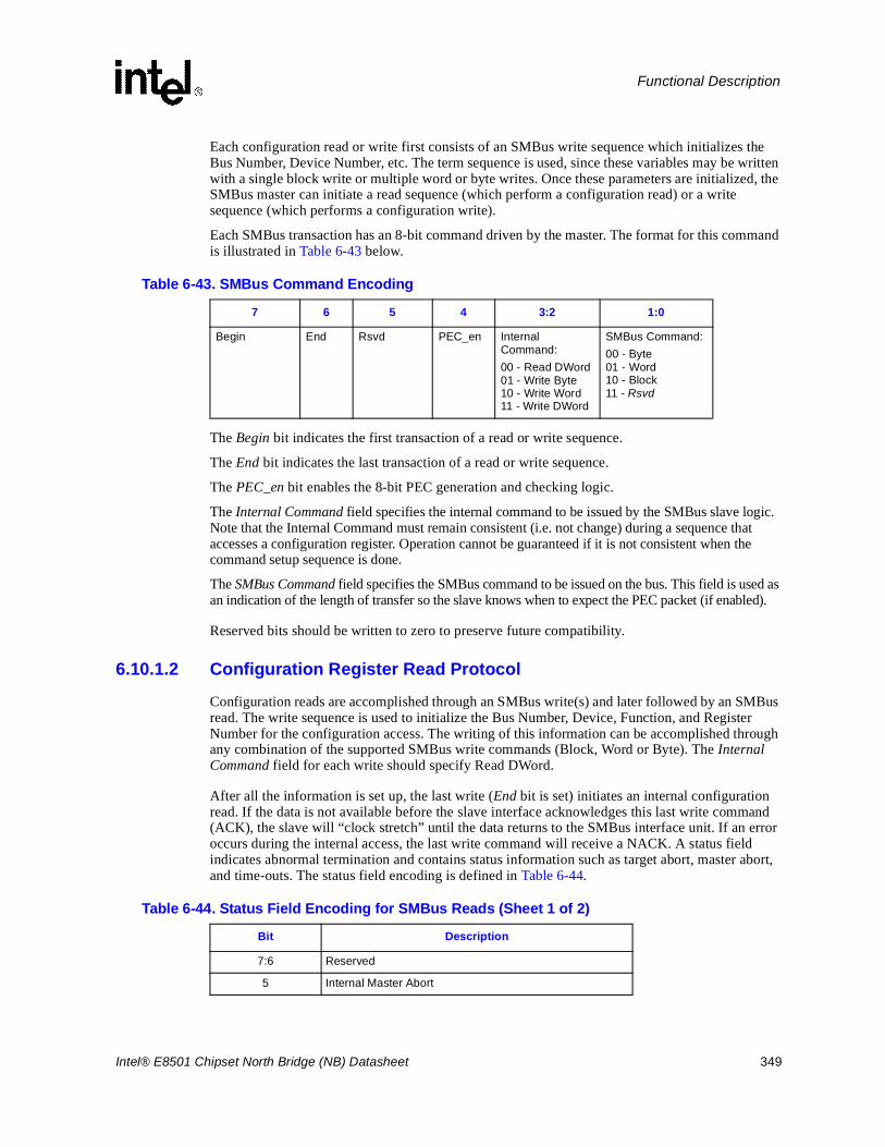
Intel® E8501 Chipset North Bridge (NB) Datasheet 349
Functional Description
Each configuration read or write first consists of an SMBus write sequence which initializes the Bus Number, Device Number, etc. The term sequence is used, since these variables may be written with a single block write or multiple word or byte writes. Once these parameters are initialized, the SMBus master can initiate a read sequence (which perform a configuration read) or a write sequence (which performs a configuration write).
Each SMBus transaction has an 8-bit command driven by the master. The format for this command is illustrated in Table 6-43 below.
The Begin bit indicates the first transaction of a read or write sequence.
The End bit indicates the last transaction of a read or write sequence.
The PEC_en bit enables the 8-bit PEC generation and checking logic.
The Internal Command field specifies the internal command to be issued by the SMBus slave logic. Note that the Internal Command must remain consistent (i.e. not change) during a sequence that accesses a configuration register. Operation cannot be guaranteed if it is not consistent when the command setup sequence is done.
The SMBus Command field specifies the SMBus command to be issued on the bus. This field is used as an indication of the length of transfer so the slave knows when to expect the PEC packet (if enabled).
Reserved bits should be written to zero to preserve future compatibility.
6.10.1.2 Configuration Register Read Protocol
Configuration reads are accomplished through an SMBus write(s) and later followed by an SMBus read. The write sequence is used to initialize the Bus Number, Device, Function, and Register Number for the configuration access. The writing of this information can be accomplished through any combination of the supported SMBus write commands (Block, Word or Byte). The InternalCommand field for each write should specify Read DWord.
After all the information is set up, the last write (End bit is set) initiates an internal configuration read. If the data is not available before the slave interface acknowledges this last write command (ACK), the slave will “clock stretch” until the data returns to the SMBus interface unit. If an error occurs during the internal access, the last write command will receive a NACK. A status field indicates abnormal termination and contains status information such as target abort, master abort, and time-outs. The status field encoding is defined in Table 6-44.
Table 6-43. SMBus Command Encoding
7 6 5 4 3:2 1:0
Begin End Rsvd PEC_en Internal Command:00 - Read DWord01 - Write Byte10 - Write Word11 - Write DWord
SMBus Command:00 - Byte01 - Word10 - Block11 - Rsvd
Table 6-44. Status Field Encoding for SMBus Reads (Sheet 1 of 2)
Bit Description
7:6 Reserved
5 Internal Master Abort
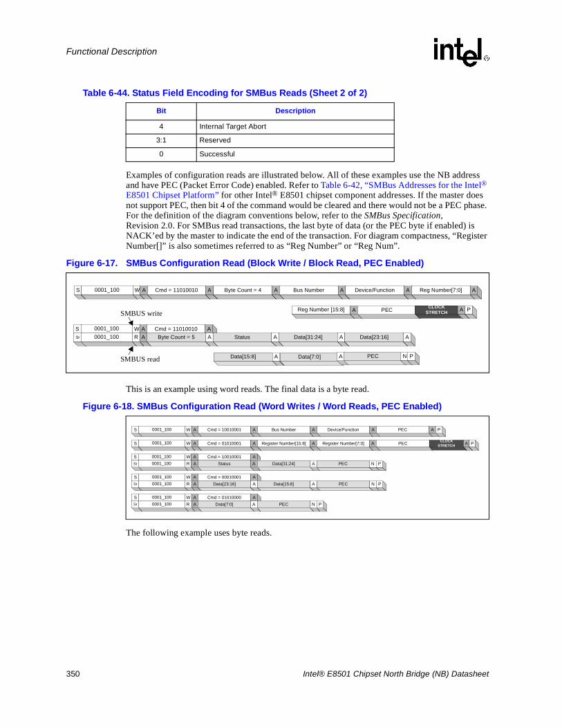
350 Intel® E8501 Chipset North Bridge (NB) Datasheet
Functional Description
Examples of configuration reads are illustrated below. All of these examples use the NB address and have PEC (Packet Error Code) enabled. Refer to Table 6-42, “SMBus Addresses for the Intel®E8501 Chipset Platform” for other Intel® E8501 chipset component addresses. If the master does not support PEC, then bit 4 of the command would be cleared and there would not be a PEC phase. For the definition of the diagram conventions below, refer to the SMBus Specification,Revision 2.0. For SMBus read transactions, the last byte of data (or the PEC byte if enabled) is NACK’ed by the master to indicate the end of the transaction. For diagram compactness, “Register Number[]” is also sometimes referred to as “Reg Number” or “Reg Num”.
This is an example using word reads. The final data is a byte read.
The following example uses byte reads.
4 Internal Target Abort
3:1 Reserved
0 Successful
Table 6-44. Status Field Encoding for SMBus Reads (Sheet 2 of 2)
Bit Description
Figure 6-17. SMBus Configuration Read (Block Write / Block Read, PEC Enabled)
S 0001_100 W A Cmd = 11010010 ASr 0001_100 R A Byte Count = 5 A Status A Data[31:24] A Data[23:16] A
Data[15:8] A Data[7:0] A
S 0001_100 W A Cmd = 11010010 A Byte Count = 4 A Bus Number A Device/Function A Reg Number[7:0] A
Reg Number [15:8] A PEC CLOCKSTRETCH A P
PEC N PSMBUS read
SMBUS write
Figure 6-18. SMBus Configuration Read (Word Writes / Word Reads, PEC Enabled)
S 0001_100 W A Cmd = 10010001 A Bus Number A Device/Function A PEC
S 0001_100 W A Cmd = 01010001 A Register Number[15:8] A
A P
S 0001_100 W A Cmd = 00010001Sr 0001_100 R A Data[23:16]
S 0001_100 W A Cmd = 01010000 ASr 0001_100 R A Data[7:0] A PEC N P
AA Data[15:8] A PEC N P
Register Number[7:0] A PEC CLOCKSTRETCH A P
S 0001_100 W A Cmd = 10010001Sr 0001_100 R A Status
AA Data[31:24] A PEC N P
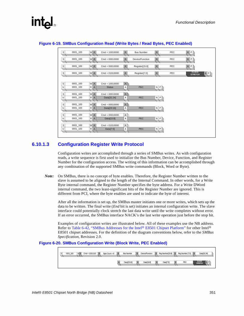
Intel® E8501 Chipset North Bridge (NB) Datasheet 351
Functional Description
6.10.1.3 Configuration Register Write Protocol
Configuration writes are accomplished through a series of SMBus writes. As with configuration reads, a write sequence is first used to initialize the Bus Number, Device, Function, and Register Number for the configuration access. The writing of this information can be accomplished through any combination of the supported SMBus write commands (Block, Word or Byte).
Note: On SMBus, there is no concept of byte enables. Therefore, the Register Number written to the slave is assumed to be aligned to the length of the Internal Command. In other words, for a Write Byte internal command, the Register Number specifies the byte address. For a Write DWord internal command, the two least-significant bits of the Register Number are ignored. This is different from PCI, where the byte enables are used to indicate the byte of interest.
After all the information is set up, the SMBus master initiates one or more writes, which sets up the data to be written. The final write (End bit is set) initiates an internal configuration write. The slave interface could potentially clock stretch the last data write until the write completes without error. If an error occurred, the SMBus interface NACK’s the last write operation just before the stop bit.
Examples of configuration writes are illustrated below. All of these examples use the NB address. Refer to Table 6-42, “SMBus Addresses for the Intel® E8501 Chipset Platform” for other Intel®E8501 chipset addresses. For the definition of the diagram conventions below, refer to the SMBusSpecification, Revision 2.0.
Figure 6-19. SMBus Configuration Read (Write Bytes / Read Bytes, PEC Enabled)
S 0001_100 W A Cmd = 10010000 A Bus Number A PEC A P
S 0001_100 W A Cmd = 00010000 A Device/Function A PEC A P
S 0001_100 W A Cmd = 01010000 A Register[7:0] A PEC
S 0001_100 W A Cmd = 00010000Sr 0001_100 R A Data[31:24]
S 0001_100 W A Cmd = 00010000 ASr 0001_100 R A Data[23:16] A PEC N P
S 0001_100 W A Cmd = 00010000 ASr 0001_100 R A Data[15:8] A PEC N P
S 0001_100 W A Cmd = 01010000 ASr 0001_100 R A Data[7:0] A PEC N P
A
CLOCKSTRETCH A P
A PEC N P
S 0001_100 W A Cmd = 10010000Sr 0001_100 R A Status
AA PEC N P
S 0001_100 W A Cmd = 00010000 A Register[15:8] A PEC A P
Figure 6-20. SMBus Configuration Write (Block Write, PEC Enabled)
A
S 0001_100 WA Cmd = 11011110 A Byte Count = 8 A Bus Number A Device/Function A Reg Number[15:8] A Reg Number [7:0] A Data[31:24]
Data[23:16] A Data[16:8] A Data[7:0] A PEC CLOCKSTRETCH A P
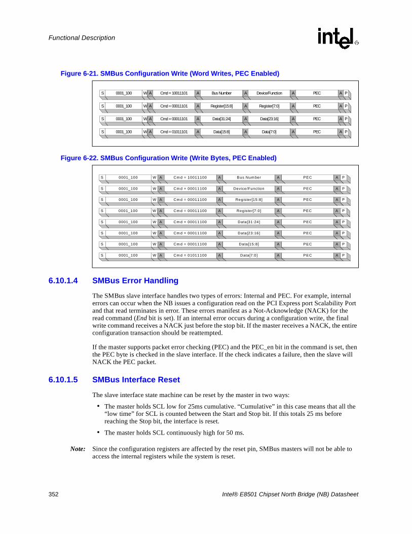
352 Intel® E8501 Chipset North Bridge (NB) Datasheet
Functional Description
6.10.1.4 SMBus Error Handling
The SMBus slave interface handles two types of errors: Internal and PEC. For example, internal errors can occur when the NB issues a configuration read on the PCI Express port Scalability Port and that read terminates in error. These errors manifest as a Not-Acknowledge (NACK) for the read command (End bit is set). If an internal error occurs during a configuration write, the final write command receives a NACK just before the stop bit. If the master receives a NACK, the entire configuration transaction should be reattempted.
If the master supports packet error checking (PEC) and the PEC_en bit in the command is set, then the PEC byte is checked in the slave interface. If the check indicates a failure, then the slave will NACK the PEC packet.
6.10.1.5 SMBus Interface Reset
The slave interface state machine can be reset by the master in two ways:
• The master holds SCL low for 25ms cumulative. “Cumulative” in this case means that all the “low time” for SCL is counted between the Start and Stop bit. If this totals 25 ms before reaching the Stop bit, the interface is reset.
• The master holds SCL continuously high for 50 ms.
Note: Since the configuration registers are affected by the reset pin, SMBus masters will not be able to access the internal registers while the system is reset.
Figure 6-21. SMBus Configuration Write (Word Writes, PEC Enabled)
S 0001_100 W A Cmd = 10011101 A Bus Number A Device/Function A PEC A P
S 0001_100 W A Cmd = 00011101 A Register[15:8] A Register[7:0] A PEC
S 0001_100 W A Cmd = 00011101 A Data[31:24] A Data[23:16] A PEC A P
S 0001_100 W A Cmd = 01011101 A Data[15:8] A
A P
Data[7:0] A PEC A P
Figure 6-22. SMBus Configuration Write (Write Bytes, PEC Enabled)
S 0001_100 W A Cm d = 10011100 A Bus Num ber A PEC A P
S 0001_100 W A Cm d = 00011100 A Device/Function A PEC A P
S 0001_100 W A Cm d = 00011100 A Register[15:8] A PEC A P
S 0001_100 W A Cm d = 01011100 A Data[7:0] A PEC A P
S 0001_100 W A Cm d = 00011100 A Data[31:24] A PEC A P
S 0001_100 W A Cm d = 00011100 A Data[23:16] A PEC A P
S 0001_100 W A Cm d = 00011100 A Data[15:8] A PEC A P
S 0001_100 W A Cm d = 00011100 A Register[7:0] A PEC A P
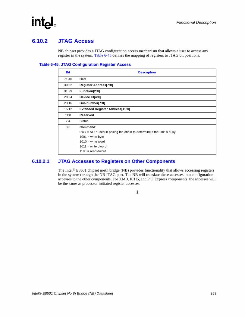
Intel® E8501 Chipset North Bridge (NB) Datasheet 353
Functional Description
6.10.2 JTAG AccessNB chipset provides a JTAG configuration access mechanism that allows a user to access any register in the system. Table 6-45 defines the mapping of registers to JTAG bit positions.
6.10.2.1 JTAG Accesses to Registers on Other Components
The Intel® E8501 chipset north bridge (NB) provides functionality that allows accessing registers in the system through the NB JTAG port. The NB will translate these accesses into configuration accesses to the other components. For XMB, ICH5, and PCI Express components, the accesses will be the same as processor initiated register accesses.
§
Table 6-45. JTAG Configuration Register Access
Bit Description
71:40 Data
39:32 Register Address[7:0]
31:29 Function[2:0]
28:24 Device ID[4:0]
23:16 Bus number[7:0]
15:12 Extended Register Address[11:8]
11:8 Reserved
7:4 Status
3:0 Command:0xxx = NOP used in polling the chain to determine if the unit is busy.1001 = write byte1010 = write word1011 = write dword1100 = read dword

354 Intel® E8501 Chipset North Bridge (NB) Datasheet
Functional Description
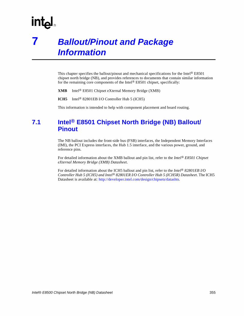
Intel® E8500 Chipset North Bridge (NB) Datasheet 355
7 Ballout/Pinout and Package Information
This chapter specifies the ballout/pinout and mechanical specifications for the Intel® E8501 chipset north bridge (NB), and provides references to documents that contain similar information for the remaining core components of the Intel® E8501 chipset, specifically:
XMB Intel® E8501 Chipset eXternal Memory Bridge (XMB)
ICH5 Intel® 82801EB I/O Controller Hub 5 (ICH5)
This information is intended to help with component placement and board routing.
7.1 Intel® E8501 Chipset North Bridge (NB) Ballout/PinoutThe NB ballout includes the front-side bus (FSB) interfaces, the Independent Memory Interfaces (IMI), the PCI Express interfaces, the Hub 1.5 interface, and the various power, ground, and reference pins.
For detailed information about the XMB ballout and pin list, refer to the Intel® E8501 Chipset eXternal Memory Bridge (XMB) Datasheet.
For detailed information about the ICH5 ballout and pin list, refer to the Intel® 82801EB I/O Controller Hub 5 (ICH5) and Intel® 82801ER I/O Controller Hub 5 (ICH5R) Datasheet. The ICH5 Datasheet is available at: http://developer.intel.com/design/chipsets/datashts.
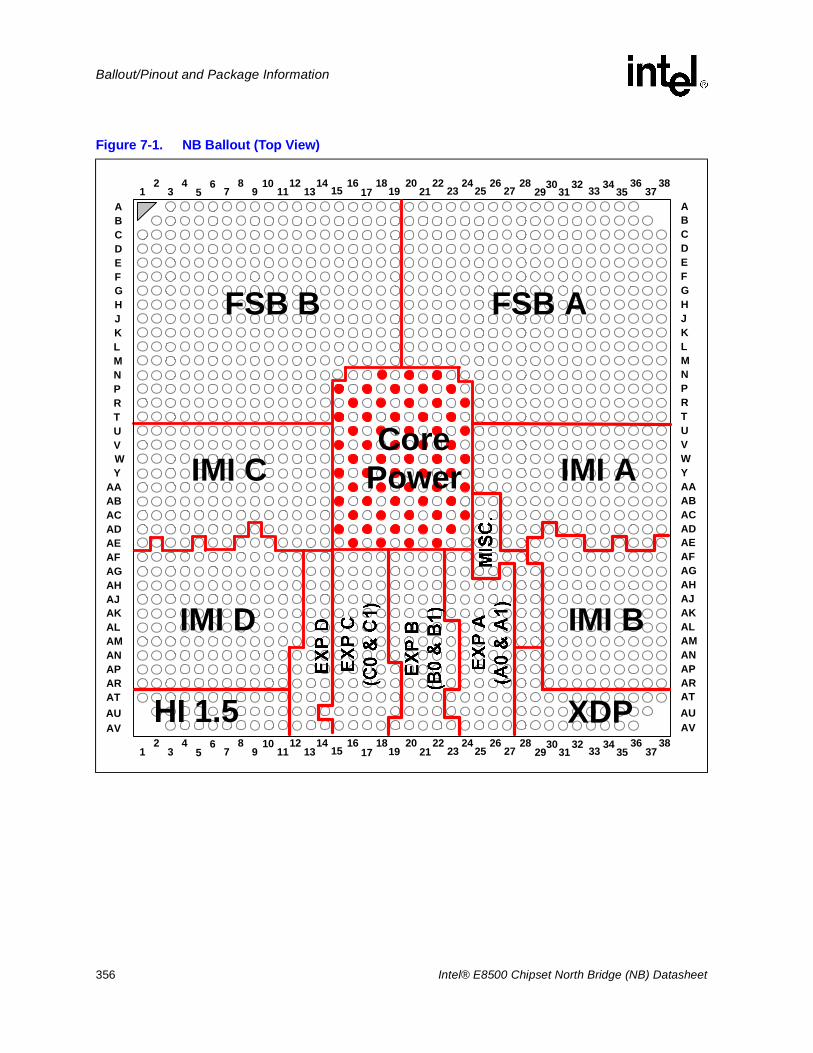
356 Intel® E8500 Chipset North Bridge (NB) Datasheet
Ballout/Pinout and Package Information
Figure 7-1. NB Ballout (Top View)
IMI B
IMI A
IMI D
IMI C
HI 1.5
FSB B FSB A
CorePower
XDPAVAUATARAPANAMALAKAJAHAGAFAEADACABAAYWVUTRPNMLKJHGFEDCBA
AVAUATARAPANAMALAKAJAHAGAFAEADACABAA
YWVUTRPNMLKJHGFEDCBA
12
34
56
78
910
1112
1314
1516
1718
1920
2122
2324
2526
2728
2930
3132 33 34
3536
3738
12
34
56
78
910
1112
1314
1516
1718
1920
2122
2324
2526
2728
2930
3132 33 34
3536
3738
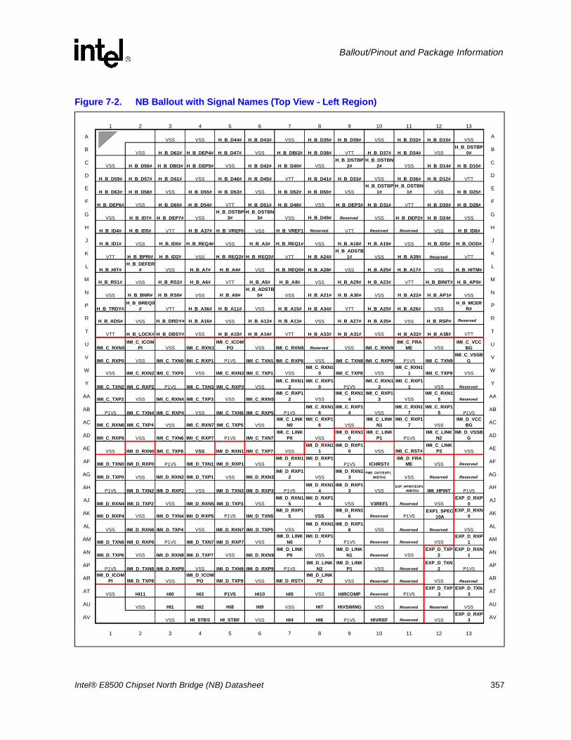
Intel® E8500 Chipset North Bridge (NB) Datasheet 357
Ballout/Pinout and Package Information
Figure 7-2. NB Ballout with Signal Names (Top View - Left Region)
1 2 3 4 5 6 7 8 9 10 11 12 13
AVSS VSS H_B_D44# H_B_D43# VSS H_B_D35# H_B_D39# VSS H_B_D32# H_B_D15# VSS
A
BVSS H_B_D62# H_B_DEP4# H_B_D47# VSS H_B_DBI2# H_B_D38# VTT H_B_D37# H_B_D34# VSS
H_B_DSTBP0#
B
CVSS H_B_D56# H_B_DBI3# H_B_DEP5# VSS H_B_D42# H_B_D40# VSS
H_B_DSTBP2#
H_B_DSTBN2# VSS H_B_D14# H_B_D10# C
D H_B_D59# H_B_D57# H_B_D61# VSS H_B_D46# H_B_D45# VTT H_B_D41# H_B_D33# VSS H_B_D36# H_B_D12# VTTD
EH_B_D63# H_B_D58# VSS H_B_D55# H_B_D53# VSS H_B_D52# H_B_D50# VSS
H_B_DSTBP1#
H_B_DSTBN1# VSS H_B_D25#
E
FH_B_DEP6# VSS H_B_D60# H_B_D54# VTT H_B_D51# H_B_D48# VSS H_B_DEP3# H_B_D31# VTT H_B_D30# H_B_D28#
F
GVSS H_B_ID7# H_B_DEP7# VSS
H_B_DSTBP3#
H_B_DSTBN3# VSS H_B_D49# Reserved VSS H_B_DEP2# H_B_D24# VSS
G
H H_B_ID4# H_B_ID5# VTT H_B_A37# H_B_VREF0 VSS H_B_VREF1 Reserved VTT Reserved Reserved VSS H_B_ID6# H
J H_B_ID1# VSS H_B_ID0# H_B_REQ4# VSS H_B_A3# H_B_REQ1# VSS H_B_A18# H_B_A19# VSS H_B_IDS# H_B_OOD# J
KVTT H_B_BPRI# H_B_ID2# VSS H_B_REQ2# H_B_REQ3# VTT H_B_A24#
H_B_ADSTB1# VSS H_B_A39# Reserved VTT
K
L H_B_HIT#H_B_DEFER
# VSS H_B_A7# H_B_A4# VSS H_B_REQ0# H_B_A28# VSS H_B_A25# H_B_A17# VSS H_B_HITM# L
M H_B_RS1# VSS H_B_RS2# H_B_A6# VTT H_B_A5# H_B_A8# VSS H_B_A29# H_B_A23# VTT H_B_BINIT# H_B_AP0# M
N VSS H_B_BNR# H_B_RS0# VSS H_B_A9#H_B_ADSTB
0# VSS H_B_A21# H_B_A30# VSS H_B_A22# H_B_AP1# VSS N
P H_B_TRDY#H_B_BREQ0
# VTT H_B_A36# H_B_A11# VSS H_B_A15# H_B_A34# VTT H_B_A20# H_B_A26# VSSH_B_MCER
R#P
R H_B_ADS# VSS H_B_DRDY# H_B_A16# VSS H_B_A12# H_B_A13# VSS H_B_A27# H_B_A35# VSS H_B_RSP# R
T VTT H_B_LOCK# H_B_DBSY# VSS H_B_A10# H_B_A14# VTT H_B_A33# H_B_A31# VSS H_B_A32# H_B_A38# VTT T
UIMI_C_RXN0
IMI_C_ICOMPI VSS IMI_C_RXN1
IMI_C_ICOMPO VSS IMI_C_RXN8 Reserved VSS IMI_C_RXN9
IMI_C_FRAME VSS
IMI_C_VCCBG
U
VIMI_C_RXP0 VSS IMI_C_TXN0 IMI_C_RXP1 P1V5 IMI_C_TXN1 IMI_C_RXP8 VSS IMI_C_TXN8 IMI_C_RXP9 P1V5 IMI_C_TXN9
IMI_C_VSSBG
V
W VSS IMI_C_RXN2 IMI_C_TXP0 VSS IMI_C_RXN3 IMI_C_TXP1 VSSIMI_C_RXN1
0 IMI_C_TXP8 VSSIMI_C_RXN1
1 IMI_C_TXP9 VSS W
YIMI_C_TXN2 IMI_C_RXP2 P1V5 IMI_C_TXN3 IMI_C_RXP3 VSS
IMI_C_RXN12
IMI_C_RXP10 P1V5
IMI_C_RXN13
IMI_C_RXP11 VSS Reserved
Y
AA IMI_C_TXP2 VSS IMI_C_RXN4 IMI_C_TXP3 VSS IMI_C_RXN5IMI_C_RXP1
2 VSSIMI_C_RXN1
4IMI_C_RXP1
3 VSSIMI_C_RXN1
5 Reserved AA
ABP1V5 IMI_C_TXN4 IMI_C_RXP4 VSS IMI_C_TXN5 IMI_C_RXP5 P1V5
IMI_C_RXN16
IMI_C_RXP14 VSS
IMI_C_RXN17
IMI_C_RXP15 P1V5
AB
AC IMI_C_RXN6 IMI_C_TXP4 VSS IMI_C_RXN7 IMI_C_TXP5 VSSIMI_C_LINK
N0IMI_C_RXP1
6 VSSIMI_C_LINK
N1IMI_C_RXP1
7 VSSIMI_D_VCC
BG AC
AD IMI_C_RXP6 VSS IMI_C_TXN6 IMI_C_RXP7 P1V5 IMI_C_TXN7IMI_C_LINK
P0 VSSIMI_D_RXN1
0IMI_C_LINK
P1 P1V5IMI_C_LINK
N2IMI_D_VSSB
G AD
AE VSS IMI_D_RXN0 IMI_C_TXP6 VSS IMI_D_RXN1 IMI_C_TXP7 VSSIMI_D_RXN1
1IMI_D_RXP1
0 VSS IMI_C_RST#IMI_C_LINK
P2 VSS AE
AF IMI_D_TXN0 IMI_D_RXP0 P1V5 IMI_D_TXN1 IMI_D_RXP1 VSSIMI_D_RXN1
2IMI_D_RXP1
1 P1V5 ICHRST#IMI_D_FRA
ME VSS Reserved AF
AG IMI_D_TXP0 VSS IMI_D_RXN2 IMI_D_TXP1 VSS IMI_D_RXN3IMI_D_RXP1
2 VSSIMI_D_RXN1
3PME_OUT/EXP1_
WIDTH2 VSS Reserved Reserved AG
AHP1V5 IMI_D_TXN2 IMI_D_RXP2 VSS IMI_D_TXN3 IMI_D_RXP3 P1V5
IMI_D_RXN14
IMI_D_RXP13 VSS
EXP_HPINT/EXP1_WIDTH1 IMI_HPINT P1V5
AH
AJIMI_D_RXN4 IMI_D_TXP2 VSS IMI_D_RXN5 IMI_D_TXP3 VSS
IMI_D_RXN15
IMI_D_RXP14 VSS V3REF1 Reserved VSS
EXP_D_RXP0
AJ
AK IMI_D_RXP4 VSS IMI_D_TXN4 IMI_D_RXP5 P1V5 IMI_D_TXN5IMI_D_RXP1
5 VSSIMI_D_RXN1
6 Reserved P1V5EXP_D_RXN
0 AK
ALVSS IMI_D_RXN6 IMI_D_TXP4 VSS IMI_D_RXN7 IMI_D_TXP5 VSS
IMI_D_RXN17
IMI_D_RXP16 VSS Reserved Reserved VSS
AL
AM IMI_D_TXN6 IMI_D_RXP6 P1V5 IMI_D_TXN7 IMI_D_RXP7 VSSIMI_D_LINK
N0IMI_D_RXP1
7 P1V5 Reserved Reserved VSSEXP_D_RXP
1 AM
AN IMI_D_TXP6 VSS IMI_D_RXN8 IMI_D_TXP7 VSS IMI_D_RXN9IMI_D_LINK
P0 VSSIMI_D_LINK
N1 Reserved VSSEXP_D_TXP
2EXP_D_RXN
1 AN
APP1V5 IMI_D_TXN8 IMI_D_RXP8 VSS IMI_D_TXN9 IMI_D_RXP9 P1V5
IMI_D_LINKN2
IMI_D_LINKP1 VSS Reserved
EXP_D_TXN2 P1V5
AP
AR IMI_D_ICOMPI IMI_D_TXP8 VSS
IMI_D_ICOMPO IMI_D_TXP9 VSS IMI_D_RST#
IMI_D_LINKP2 VSS Reserved Reserved VSS Reserved AR
AT VSS HI11 HI0 HI3 P1V5 HI10 HI5 VSS HIRCOMP Reserved P1V5EXP_D_TXP
3EXP_D_TXN
3 AT
AU VSS HI1 HI2 HI8 HI9 VSS HI7 HIVSWING VSS Reserved Reserved VSS AU
AV VSS HI_STBS HI_STBF VSS HI4 HI6 P1V5 HIVREF Reserved VSSEXP_D_RXP
3 AV
1 2 3 4 5 6 7 8 9 10 11 12 13
EXP1_SPEC10A
Reserved
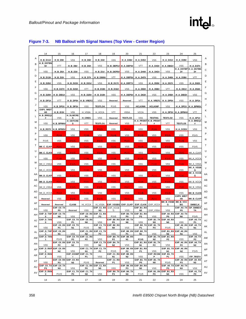
358 Intel® E8500 Chipset North Bridge (NB) Datasheet
Ballout/Pinout and Package Information
Figure 7-3. NB Ballout with Signal Names (Top View - Center Region)
14 15 16 17 18 19 20 21 22 23 24 25
AH_B_D11# H_B_D9# VSS H_B_D8# H_B_D4# VSS H_A_D46# H_A_D45# VSS H_A_D41# H_A_D39# VSS
A
B H_B_DSTBN0# VTT H_B_D6# H_B_D0# VSS H_B_DEP1# H_A_DEP4# VTT H_A_D43# H_A_DBI2# VSS H_A_D37#
B
CVSS H_B_D5# H_B_D3# VSS H_B_D1# H_B_DEP0# VSS H_A_D44# H_A_D42# VSS
H_A_DSTBP2#
H_A_DSTBN2#
C
DH_B_D13# H_B_D2# VSS H_B_D7# H_B_DBI0# VTT H_A_DEP5# H_A_D47# VSS H_A_D40# H_A_D38# VTT
D
EH_B_D26# VSS H_B_D22# H_B_D21# VSS H_B_D17# H_A_DEP7# VSS H_A_D59# H_A_D57# VSS H_A_D62#
E
FVSS H_B_D27# H_B_D23# VTT H_B_D18# H_B_D16# VSS H_A_D60# H_A_D58# VTT H_A_D61# H_A_D54#
F
GH_B_D29# H_B_DBI1# VSS H_B_D20# H_B_D19# VSS H_A_DEP6# H_A_D63# VSS H_A_D56# H_A_DBI3# VSS
G
HH_B_DP1# VTT H_B_DP0# H_B_VREF2 VSS Reserved Reserved VTT H_A_VREF1 H_A_DP0# VSS H_A_DP1#
H
JVSS H_B_DP2# H_B_DP3# VSS TESTLO4 P1V5 VSS HCLKINN HCLKINP VSS H_A_DP2# H_A_BPM5#
J
K EXP1_WIDTH0 H_B_ID3# VSS H_VSSA H_VCCA VTT VSSA VCCA VSS H_A_DP3# H_A_BPM4# VTT
K
L H_B_BREQ1# VSS
H_SLWCRES H_CRES VSS Reserved TESTLO3 VSS TESTHI1 TESTLO2 VSS H_A_AP1#
L
M VSS H_B_BPM4#H_ODTCRE
S VTT TESTLO1 Reserved VSSH_A_PRSNT
#H_B_PRSNT
# VTT TESTLO5H_A_BREQ1
# M
N H_B_RST# H_B_BPM5# VSS VSS P1V5 VSS P1V5 VSS P1V5 VSS H_A_OOD# VSS N
PVSS P1V5 VSS P1V5 VSS P1V5 VSS P1V5 VSS P1V5 VSS P1V5
P
R P1V5 VSS P1V5 VSS P1V5 VSS P1V5 VSS P1V5 VSS P1V5 VSS R
T IMI_C_CLKP P1V5 VSS P1V5 VSS P1V5 VSS P1V5 VSS P1V5 VSS P1V5 T
UIMI_C_CLKN VSS P1V5 VSS P1V5 VSS P1V5 VSS P1V5 VSS P1V5 IMI_A_CLKP
U
VVSS P1V5 VSS P1V5 VSS P1V5 VSS P1V5 VSS P1V5 VSS IMI_A_VCCA
V
W IMI_C_VSSA VSS P1V5 VSS P1V5 VSS P1V5 VSS P1V5 VSS P1V5 IMI_A_VSSA W
YIMI_C_VCCA P1V5 VSS P1V5 VSS P1V5 VSS P1V5 VSS P1V5 VSS
IMI_A_VSSBG
Y
AA IMI_D_CLKP VSS P1V5 VSS P1V5 VSS P1V5 VSS P1V5 VSS P1V5IMI_A_VCCB
G AA
ABIMI_D_CLKN P1V5 VSS P1V5 VSS P1V5 VSS P1V5 VSS P1V5 VSS IMI_B_VCCA
AB
AC IMI_D_VSSA VSS P1V5 VSS P1V5 VSS P1V5 VSS P1V5 VSS P1V5 IMI_B_VSSA AC
AD IMI_D_VCCA P1V5 VSS P1V5 VSS P1V5 VSS P1V5 VSS P1V5 VSS IMI_B_CLKN AD
AE Reserved VSS P1V5 VSS P1V5 VSS P1V5 VSS P1V5 VSSEXP0_WIDT
H0 IMI_B_CLKP AE
AF Reserved Reserved CLK66 HI_VCCA HI_VSSA EXP_VSSBG EXP_CLKP EXP_CLKN EXP_VCCAIMI_B_VSSB
GIMI_B_VCC
BG SMBCLK AF
AG VSSEXP_C0_TX
P0 Reserved VSSEXP_C1_RX
N3EXP_VCCB
G VSSEXP_B1_RX
N3 EXP_VSSA VSSEXP_A0_TX
P0GP_SMBDA
TA AG
AH EXP_D_TXP0
EXP_C0_TXN0 VSS
EXP_C0_RXP0
EXP_C1_RXP3 P1V5
EXP_B0_TXP0
EXP_B1_RXP3 VSS
EXP_A0_RXP0
EXP_A0_TXN0 P1V5
AH
AJ EXP_D_TXN0 VSS
EXP_C0_TXP1
EXP_C0_RXN0 VSS
EXP_B0_RXP0
EXP_B0_TXN0 VSS
EXP_B1_TXN3
EXP_A0_RXN0 VSS
EXP_A0_TXP1
AJ
AK VSSEXP_C0_RX
P1EXP_C0_TX
N1 P1V5EXP_C1_TX
N3EXP_B0_RX
N0 VSSEXP_B0_TX
P1EXP_B1_TX
P3 P1V5EXP_A0_RX
P1EXP_A0_TX
N1 AK
AL EXP_D_TXP1
EXP_C0_RXN1 VSS
EXP_C1_RXN2
EXP_C1_TXP3 VSS
EXP_B0_RXP1
EXP_B0_TXN1 VSS
EXP_B1_RXN2
EXP_A0_RXN1 VSS
AL
AM EXP_D_TXN1 P1V5
EXP_C0_TXP2
EXP_C1_RXP2 VSS
EXP_B0_TXP2
EXP_B0_RXN1 P1V5
EXP_B1_TXN2
EXP_B1_RXP2 VSS
EXP_A0_TXP2 AM
AN VSSEXP_C0_RX
P2EXP_C0_TX
N2 VSSEXP_C1_TX
N2EXP_B0_TX
N2 VSSEXP_B1_RX
N1EXP_B1_TX
P2 VSSEXP_A0_RX
P2EXP_A0_TX
N2 AN
AP EXP_D_RXP2
EXP_C0_RXN2 VSS
EXP_C1_TXN1
EXP_C1_TXP2 P1V5
EXP_B0_RXP2
EXP_B1_RXP1 VSS
EXP_B1_TXN1
EXP_A0_RXN2 P1V5
AP
AR EXP_D_RXN2 VSS
EXP_ICOMPI
EXP_C1_TXP1 VSS
EXP_C1_RXN1
EXP_B0_RXN2 VSS
EXP_RCOMP
EXP_B1_TXP1 VSS ITP_TRST# AR
AT VSSEXP_C0_RX
P3EXP_C0_RX
N3 P1V5 ReservedEXP_C1_RX
P1 VSSEXP_B1_TX
P0EXP_B1_TX
N0 P1V5EXP_A0_RX
P3EXP_A0_RX
N3 AT
AU EXP_C0_TXP3
EXP_C0_TXN3 VSS
EXP_C1_RXP0
EXP_C1_RXN0 VSS
EXP_B0_RXP3
EXP_B0_RXN3 VSS
EXP_A0_TXP3
EXP_A0_TXN3 VSS AU
AV EXP_D_RXN3 P1V5
EXP_C1_TXP0
EXP_C1_TXN0 VSS
EXP_B0_TXP3
EXP_B0_TXN3 P1V5
EXP_B1_RXP0
EXP_B1_RXN0 VSS
EXP_A1_TXP0 AV
14 15 16 17 18 19 20 21 22 23 24 25
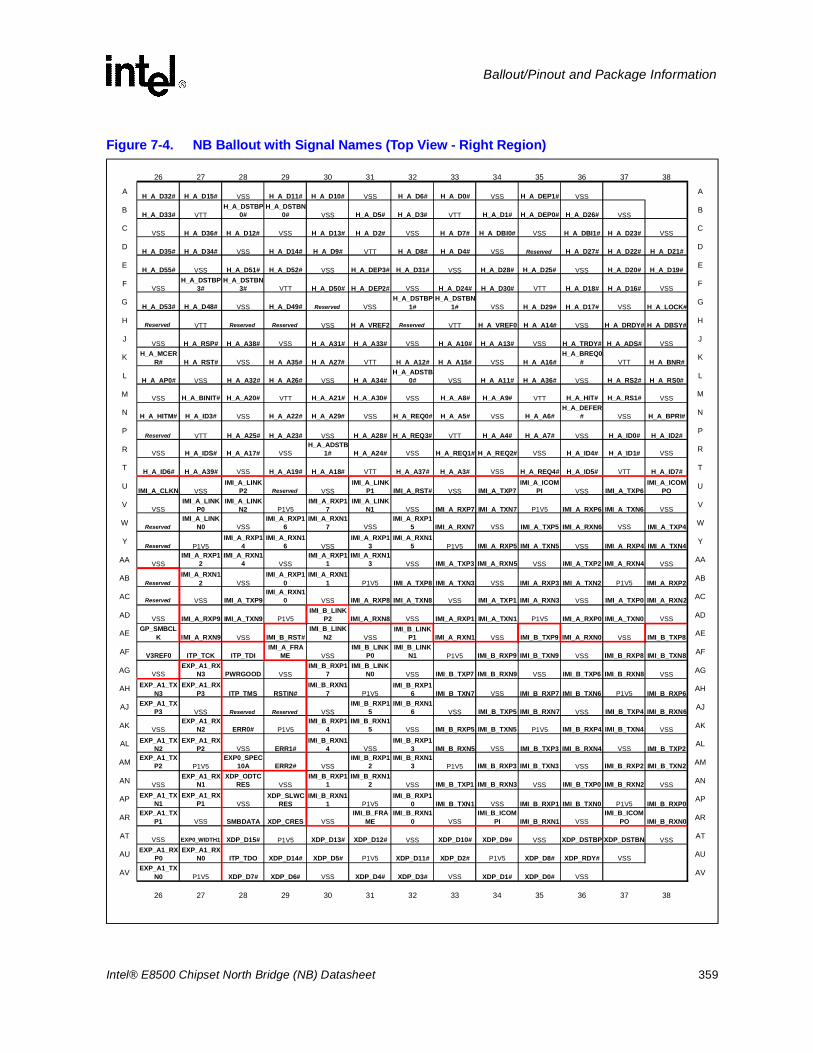
Intel® E8500 Chipset North Bridge (NB) Datasheet 359
Ballout/Pinout and Package Information
Figure 7-4. NB Ballout with Signal Names (Top View - Right Region)
26 27 28 29 30 31 32 33 34 35 36 37 38
A H_A_D32# H_A_D15# VSS H_A_D11# H_A_D10# VSS H_A_D6# H_A_D0# VSS H_A_DEP1# VSSA
B H_A_D33# VTTH_A_DSTBP
0#H_A_DSTBN
0# VSS H_A_D5# H_A_D3# VTT H_A_D1# H_A_DEP0# H_A_D26# VSSB
CVSS H_A_D36# H_A_D12# VSS H_A_D13# H_A_D2# VSS H_A_D7# H_A_DBI0# VSS H_A_DBI1# H_A_D23# VSS
C
D H_A_D35# H_A_D34# VSS H_A_D14# H_A_D9# VTT H_A_D8# H_A_D4# VSS Reserved H_A_D27# H_A_D22# H_A_D21# D
E H_A_D55# VSS H_A_D51# H_A_D52# VSS H_A_DEP3# H_A_D31# VSS H_A_D28# H_A_D25# VSS H_A_D20# H_A_D19# E
FVSS
H_A_DSTBP3#
H_A_DSTBN3# VTT H_A_D50# H_A_DEP2# VSS H_A_D24# H_A_D30# VTT H_A_D18# H_A_D16# VSS
F
G H_A_D53# H_A_D48# VSS H_A_D49# Reserved VSSH_A_DSTBP
1#H_A_DSTBN
1# VSS H_A_D29# H_A_D17# VSS H_A_LOCK#G
HVTT Reserved Reserved VSS H_A_VREF2 Reserved VTT H_A_VREF0 H_A_A14# VSS H_A_DRDY# H_A_DBSY# H
JVSS H_A_RSP# H_A_A38# VSS H_A_A31# H_A_A33# VSS H_A_A10# H_A_A13# VSS H_A_TRDY# H_A_ADS# VSS
J
K H_A_MCERR# H_A_RST# VSS H_A_A35# H_A_A27# VTT H_A_A12# H_A_A15# VSS H_A_A16#
H_A_BREQ0# VTT H_A_BNR#
K
L H_A_AP0# VSS H_A_A32# H_A_A26# VSS H_A_A34#H_A_ADSTB
0# VSS H_A_A11# H_A_A36# VSS H_A_RS2# H_A_RS0# L
M VSS H_A_BINIT# H_A_A20# VTT H_A_A21# H_A_A30# VSS H_A_A8# H_A_A9# VTT H_A_HIT# H_A_RS1# VSS M
N H_A_HITM# H_A_ID3# VSS H_A_A22# H_A_A29# VSS H_A_REQ0# H_A_A5# VSS H_A_A6#H_A_DEFER
# VSS H_A_BPRI# N
PReserved VTT H_A_A25# H_A_A23# VSS H_A_A28# H_A_REQ3# VTT H_A_A4# H_A_A7# VSS H_A_ID0# H_A_ID2# P
R VSS H_A_IDS# H_A_A17# VSSH_A_ADSTB
1# H_A_A24# VSS H_A_REQ1# H_A_REQ2# VSS H_A_ID4# H_A_ID1# VSS R
T H_A_ID6# H_A_A39# VSS H_A_A19# H_A_A18# VTT H_A_A37# H_A_A3# VSS H_A_REQ4# H_A_ID5# VTT H_A_ID7# T
U IMI_A_CLKN VSSIMI_A_LINK
P2 Reserved VSSIMI_A_LINK
P1 IMI_A_RST# VSS IMI_A_TXP7IMI_A_ICOM
PI VSS IMI_A_TXP6IMI_A_ICOM
PO U
VVSS
IMI_A_LINKP0
IMI_A_LINKN2 P1V5
IMI_A_RXP17
IMI_A_LINKN1 VSS IMI_A_RXP7 IMI_A_TXN7 P1V5 IMI_A_RXP6 IMI_A_TXN6 VSS
V
W ReservedIMI_A_LINK
N0 VSSIMI_A_RXP1
6IMI_A_RXN1
7 VSSIMI_A_RXP1
5 IMI_A_RXN7 VSS IMI_A_TXP5 IMI_A_RXN6 VSS IMI_A_TXP4 W
YReserved P1V5
IMI_A_RXP14
IMI_A_RXN16 VSS
IMI_A_RXP13
IMI_A_RXN15 P1V5 IMI_A_RXP5 IMI_A_TXN5 VSS IMI_A_RXP4 IMI_A_TXN4 Y
AA VSSIMI_A_RXP1
2IMI_A_RXN1
4 VSSIMI_A_RXP1
1IMI_A_RXN1
3 VSS IMI_A_TXP3 IMI_A_RXN5 VSS IMI_A_TXP2 IMI_A_RXN4 VSS AA
ABReserved
IMI_A_RXN12 VSS
IMI_A_RXP10
IMI_A_RXN11 P1V5 IMI_A_TXP8 IMI_A_TXN3 VSS IMI_A_RXP3 IMI_A_TXN2 P1V5 IMI_A_RXP2
AB
AC Reserved VSS IMI_A_TXP9IMI_A_RXN1
0 VSS IMI_A_RXP8 IMI_A_TXN8 VSS IMI_A_TXP1 IMI_A_RXN3 VSS IMI_A_TXP0 IMI_A_RXN2 AC
AD VSS IMI_A_RXP9 IMI_A_TXN9 P1V5IMI_B_LINK
P2 IMI_A_RXN8 VSS IMI_A_RXP1 IMI_A_TXN1 P1V5 IMI_A_RXP0 IMI_A_TXN0 VSS AD
AE GP_SMBCLK IMI_A_RXN9 VSS IMI_B_RST#
IMI_B_LINKN2 VSS
IMI_B_LINKP1 IMI_A_RXN1 VSS IMI_B_TXP9 IMI_A_RXN0 VSS IMI_B_TXP8 AE
AF V3REF0 ITP_TCK ITP_TDIIMI_A_FRA
ME VSSIMI_B_LINK
P0IMI_B_LINK
N1 P1V5 IMI_B_RXP9 IMI_B_TXN9 VSS IMI_B_RXP8 IMI_B_TXN8 AF
AG VSSEXP_A1_RX
N3 PWRGOOD VSSIMI_B_RXP1
7IMI_B_LINK
N0 VSS IMI_B_TXP7 IMI_B_RXN9 VSS IMI_B_TXP6 IMI_B_RXN8 VSS AG
AH EXP_A1_TXN3
EXP_A1_RXP3 ITP_TMS RSTIN#
IMI_B_RXN17 P1V5
IMI_B_RXP16 IMI_B_TXN7 VSS IMI_B_RXP7 IMI_B_TXN6 P1V5 IMI_B_RXP6
AH
AJ EXP_A1_TXP3 VSS Reserved Reserved VSS
IMI_B_RXP15
IMI_B_RXN16 VSS IMI_B_TXP5 IMI_B_RXN7 VSS IMI_B_TXP4 IMI_B_RXN6 AJ
AK VSSEXP_A1_RX
N2 ERR0# P1V5IMI_B_RXP1
4IMI_B_RXN1
5 VSS IMI_B_RXP5 IMI_B_TXN5 P1V5 IMI_B_RXP4 IMI_B_TXN4 VSS AK
AL EXP_A1_TXN2
EXP_A1_RXP2 VSS ERR1#
IMI_B_RXN14 VSS
IMI_B_RXP13 IMI_B_RXN5 VSS IMI_B_TXP3 IMI_B_RXN4 VSS IMI_B_TXP2
AL
AM EXP_A1_TXP2 P1V5
EXP0_SPEC10A ERR2# VSS
IMI_B_RXP12
IMI_B_RXN13 P1V5 IMI_B_RXP3 IMI_B_TXN3 VSS IMI_B_RXP2 IMI_B_TXN2 AM
AN VSSEXP_A1_RX
N1XDP_ODTC
RES VSSIMI_B_RXP1
1IMI_B_RXN1
2 VSS IMI_B_TXP1 IMI_B_RXN3 VSS IMI_B_TXP0 IMI_B_RXN2 VSS AN
AP EXP_A1_TXN1
EXP_A1_RXP1 VSS
XDP_SLWCRES
IMI_B_RXN11 P1V5
IMI_B_RXP10 IMI_B_TXN1 VSS IMI_B_RXP1 IMI_B_TXN0 P1V5 IMI_B_RXP0
AP
AR EXP_A1_TXP1 VSS SMBDATA XDP_CRES VSS
IMI_B_FRAME
IMI_B_RXN10 VSS
IMI_B_ICOMPI IMI_B_RXN1 VSS
IMI_B_ICOMPO IMI_B_RXN0 AR
AT VSS EXP0_WIDTH1 XDP_D15# P1V5 XDP_D13# XDP_D12# VSS XDP_D10# XDP_D9# VSS XDP_DSTBP XDP_DSTBN VSS AT
AU EXP_A1_RXP0
EXP_A1_RXN0 ITP_TDO XDP_D14# XDP_D5# P1V5 XDP_D11# XDP_D2# P1V5 XDP_D8# XDP_RDY# VSS AU
AV EXP_A1_TXN0 P1V5 XDP_D7# XDP_D6# VSS XDP_D4# XDP_D3# VSS XDP_D1# XDP_D0# VSS 0 0 AV
26 27 28 29 30 31 32 33 34 35 36 37 38
Reserved
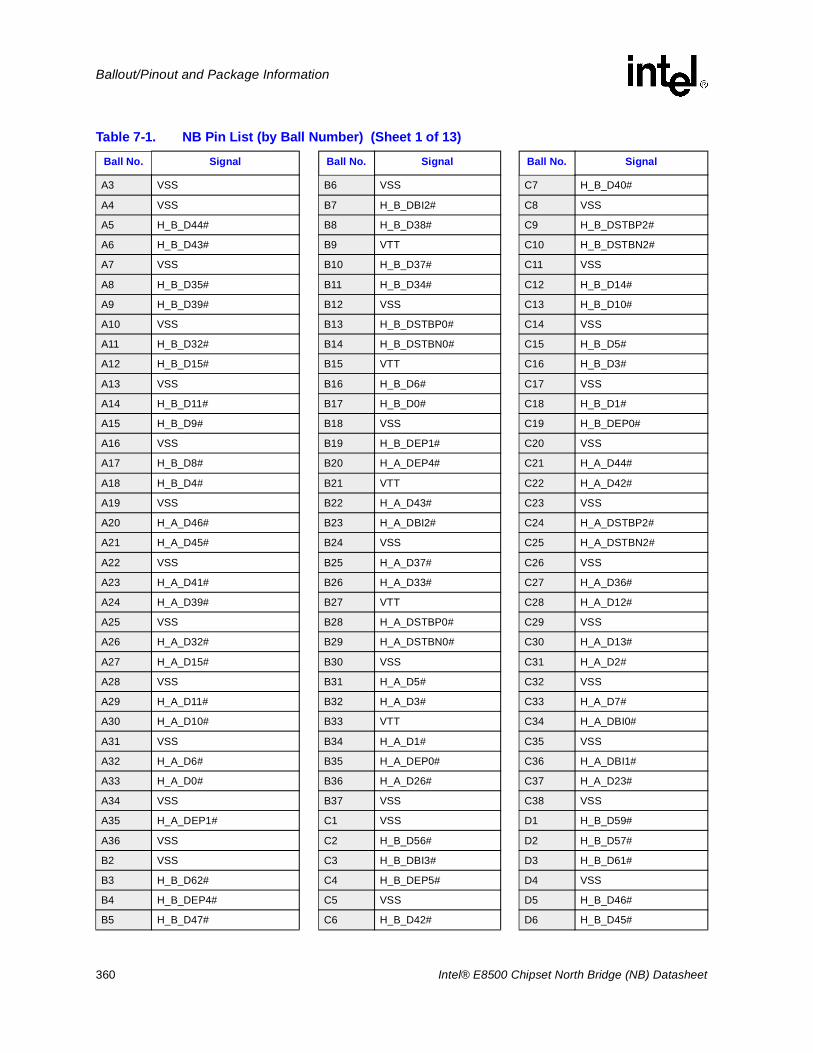
360 Intel® E8500 Chipset North Bridge (NB) Datasheet
Ballout/Pinout and Package Information
Table 7-1. NB Pin List (by Ball Number) (Sheet 1 of 13)
Ball No. Signal Ball No. Signal Ball No. Signal
A3 VSS B6 VSS C7 H_B_D40#
A4 VSS B7 H_B_DBI2# C8 VSS
A5 H_B_D44# B8 H_B_D38# C9 H_B_DSTBP2#
A6 H_B_D43# B9 VTT C10 H_B_DSTBN2#
A7 VSS B10 H_B_D37# C11 VSS
A8 H_B_D35# B11 H_B_D34# C12 H_B_D14#
A9 H_B_D39# B12 VSS C13 H_B_D10#
A10 VSS B13 H_B_DSTBP0# C14 VSS
A11 H_B_D32# B14 H_B_DSTBN0# C15 H_B_D5#
A12 H_B_D15# B15 VTT C16 H_B_D3#
A13 VSS B16 H_B_D6# C17 VSS
A14 H_B_D11# B17 H_B_D0# C18 H_B_D1#
A15 H_B_D9# B18 VSS C19 H_B_DEP0#
A16 VSS B19 H_B_DEP1# C20 VSS
A17 H_B_D8# B20 H_A_DEP4# C21 H_A_D44#
A18 H_B_D4# B21 VTT C22 H_A_D42#
A19 VSS B22 H_A_D43# C23 VSS
A20 H_A_D46# B23 H_A_DBI2# C24 H_A_DSTBP2#
A21 H_A_D45# B24 VSS C25 H_A_DSTBN2#
A22 VSS B25 H_A_D37# C26 VSS
A23 H_A_D41# B26 H_A_D33# C27 H_A_D36#
A24 H_A_D39# B27 VTT C28 H_A_D12#
A25 VSS B28 H_A_DSTBP0# C29 VSS
A26 H_A_D32# B29 H_A_DSTBN0# C30 H_A_D13#
A27 H_A_D15# B30 VSS C31 H_A_D2#
A28 VSS B31 H_A_D5# C32 VSS
A29 H_A_D11# B32 H_A_D3# C33 H_A_D7#
A30 H_A_D10# B33 VTT C34 H_A_DBI0#
A31 VSS B34 H_A_D1# C35 VSS
A32 H_A_D6# B35 H_A_DEP0# C36 H_A_DBI1#
A33 H_A_D0# B36 H_A_D26# C37 H_A_D23#
A34 VSS B37 VSS C38 VSS
A35 H_A_DEP1# C1 VSS D1 H_B_D59#
A36 VSS C2 H_B_D56# D2 H_B_D57#
B2 VSS C3 H_B_DBI3# D3 H_B_D61#
B3 H_B_D62# C4 H_B_DEP5# D4 VSS
B4 H_B_DEP4# C5 VSS D5 H_B_D46#
B5 H_B_D47# C6 H_B_D42# D6 H_B_D45#
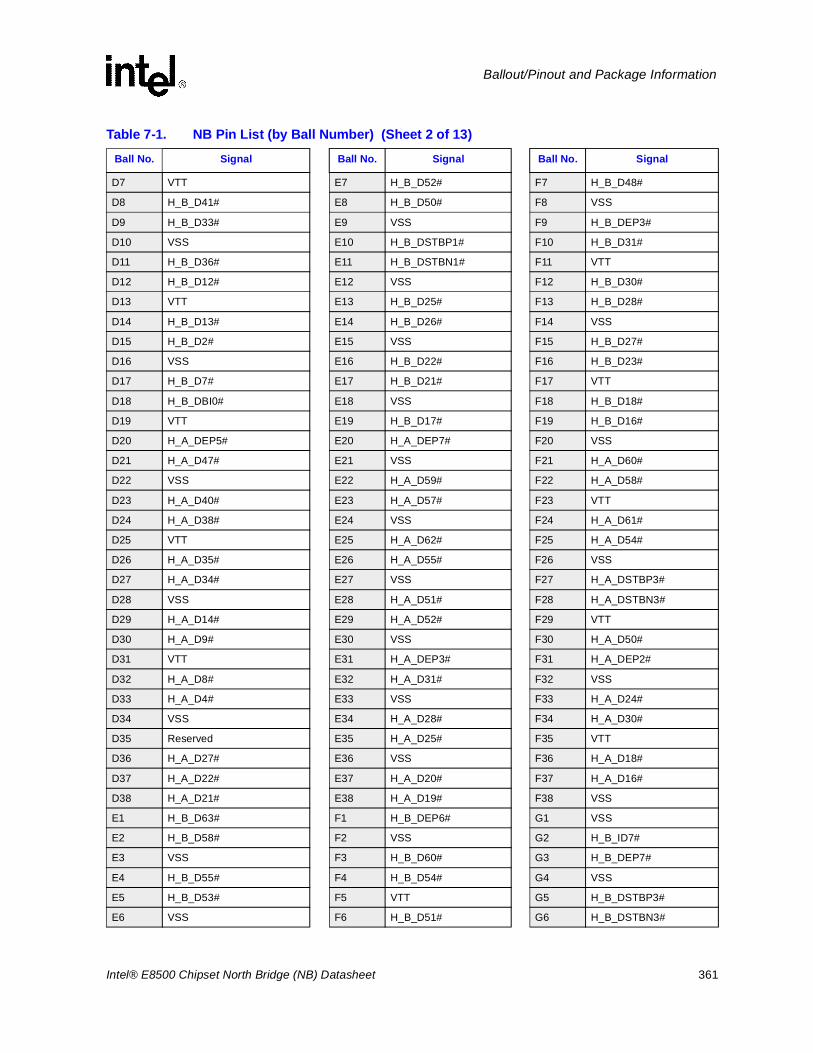
Intel® E8500 Chipset North Bridge (NB) Datasheet 361
Ballout/Pinout and Package Information
D7 VTT E7 H_B_D52# F7 H_B_D48#
D8 H_B_D41# E8 H_B_D50# F8 VSS
D9 H_B_D33# E9 VSS F9 H_B_DEP3#
D10 VSS E10 H_B_DSTBP1# F10 H_B_D31#
D11 H_B_D36# E11 H_B_DSTBN1# F11 VTT
D12 H_B_D12# E12 VSS F12 H_B_D30#
D13 VTT E13 H_B_D25# F13 H_B_D28#
D14 H_B_D13# E14 H_B_D26# F14 VSS
D15 H_B_D2# E15 VSS F15 H_B_D27#
D16 VSS E16 H_B_D22# F16 H_B_D23#
D17 H_B_D7# E17 H_B_D21# F17 VTT
D18 H_B_DBI0# E18 VSS F18 H_B_D18#
D19 VTT E19 H_B_D17# F19 H_B_D16#
D20 H_A_DEP5# E20 H_A_DEP7# F20 VSS
D21 H_A_D47# E21 VSS F21 H_A_D60#
D22 VSS E22 H_A_D59# F22 H_A_D58#
D23 H_A_D40# E23 H_A_D57# F23 VTT
D24 H_A_D38# E24 VSS F24 H_A_D61#
D25 VTT E25 H_A_D62# F25 H_A_D54#
D26 H_A_D35# E26 H_A_D55# F26 VSS
D27 H_A_D34# E27 VSS F27 H_A_DSTBP3#
D28 VSS E28 H_A_D51# F28 H_A_DSTBN3#
D29 H_A_D14# E29 H_A_D52# F29 VTT
D30 H_A_D9# E30 VSS F30 H_A_D50#
D31 VTT E31 H_A_DEP3# F31 H_A_DEP2#
D32 H_A_D8# E32 H_A_D31# F32 VSS
D33 H_A_D4# E33 VSS F33 H_A_D24#
D34 VSS E34 H_A_D28# F34 H_A_D30#
D35 Reserved E35 H_A_D25# F35 VTT
D36 H_A_D27# E36 VSS F36 H_A_D18#
D37 H_A_D22# E37 H_A_D20# F37 H_A_D16#
D38 H_A_D21# E38 H_A_D19# F38 VSS
E1 H_B_D63# F1 H_B_DEP6# G1 VSS
E2 H_B_D58# F2 VSS G2 H_B_ID7#
E3 VSS F3 H_B_D60# G3 H_B_DEP7#
E4 H_B_D55# F4 H_B_D54# G4 VSS
E5 H_B_D53# F5 VTT G5 H_B_DSTBP3#
E6 VSS F6 H_B_D51# G6 H_B_DSTBN3#
Table 7-1. NB Pin List (by Ball Number) (Sheet 2 of 13)
Ball No. Signal Ball No. Signal Ball No. Signal
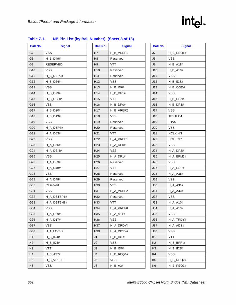
362 Intel® E8500 Chipset North Bridge (NB) Datasheet
Ballout/Pinout and Package Information
G7 VSS H7 H_B_VREF1 J7 H_B_REQ1#
G8 H_B_D49# H8 Reserved J8 VSS
G9 RESERVED H9 VTT J9 H_B_A18#
G10 VSS H10 Reserved J10 H_B_A19#
G11 H_B_DEP2# H11 Reserved J11 VSS
G12 H_B_D24# H12 VSS J12 H_B_IDS#
G13 VSS H13 H_B_ID6# J13 H_B_OOD#
G14 H_B_D29# H14 H_B_DP1# J14 VSS
G15 H_B_DBI1# H15 VTT J15 H_B_DP2#
G16 VSS H16 H_B_DP0# J16 H_B_DP3#
G17 H_B_D20# H17 H_B_VREF2 J17 VSS
G18 H_B_D19# H18 VSS J18 TESTLO4
G19 VSS H19 Reserved J19 P1V5
G20 H_A_DEP6# H20 Reserved J20 VSS
G21 H_A_D63# H21 VTT J21 HCLKINN
G22 VSS H22 H_A_VREF1 J22 HCLKINP
G23 H_A_D56# H23 H_A_DP0# J23 VSS
G24 H_A_DBI3# H24 VSS J24 H_A_DP2#
G25 VSS H25 H_A_DP1# J25 H_A_BPM5#
G26 H_A_D53# H26 Reserved J26 VSS
G27 H_A_D48# H27 VTT J27 H_A_RSP#
G28 VSS H28 Reserved J28 H_A_A38#
G29 H_A_D49# H29 Reserved J29 VSS
G30 Reserved H30 VSS J30 H_A_A31#
G31 VSS H31 H_A_VREF2 J31 H_A_A33#
G32 H_A_DSTBP1# H32 Reserved J32 VSS
G33 H_A_DSTBN1# H33 VTT J33 H_A_A10#
G34 VSS H34 H_A_VREF0 J34 H_A_A13#
G35 H_A_D29# H35 H_A_A14# J35 VSS
G36 H_A_D17# H36 VSS J36 H_A_TRDY#
G37 VSS H37 H_A_DRDY# J37 H_A_ADS#
G38 H_A_LOCK# H38 H_A_DBSY# J38 VSS
H1 H_B_ID4# J1 H_B_ID1# K1 VTT
H2 H_B_ID5# J2 VSS K2 H_B_BPRI#
H3 VTT J3 H_B_ID0# K3 H_B_ID2#
H4 H_B_A37# J4 H_B_REQ4# K4 VSS
H5 H_B_VREF0 J5 VSS K5 H_B_REQ2#
H6 VSS J6 H_B_A3# K6 H_B_REQ3#
Table 7-1. NB Pin List (by Ball Number) (Sheet 3 of 13)
Ball No. Signal Ball No. Signal Ball No. Signal
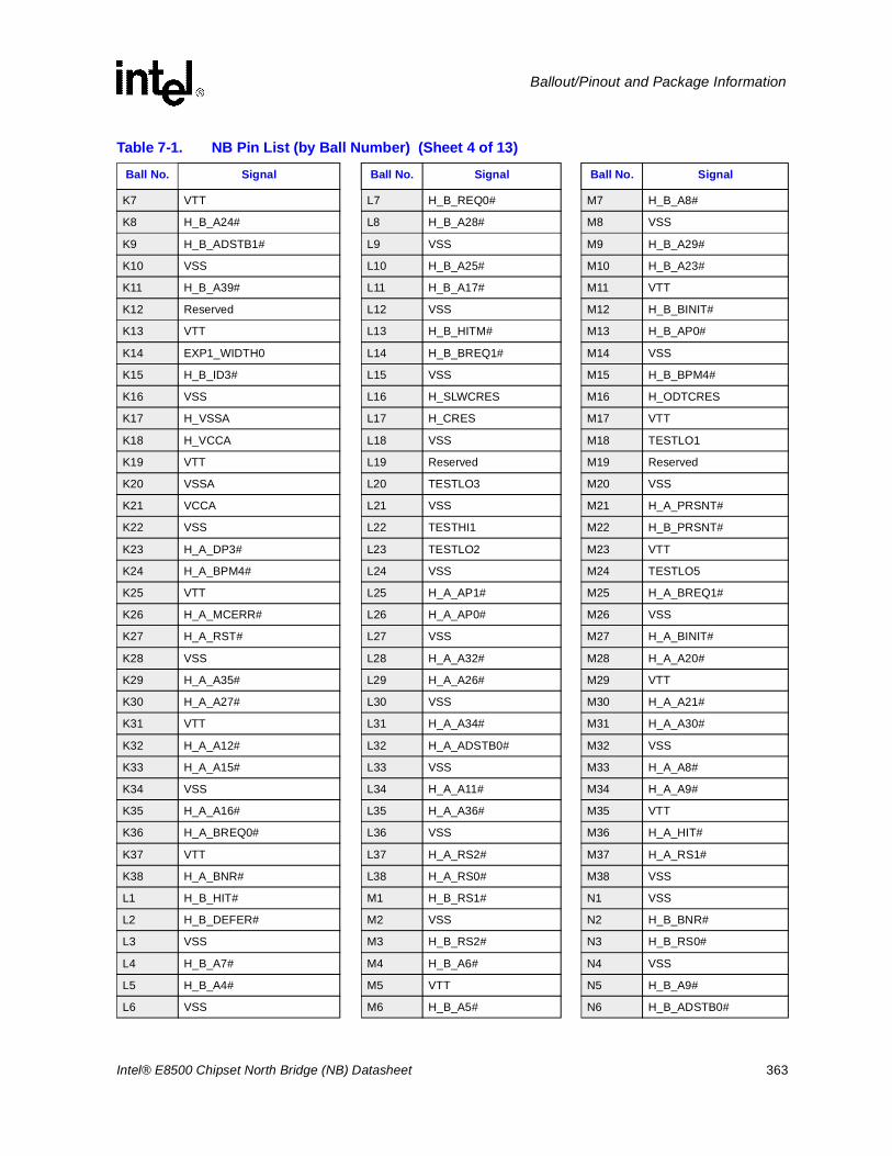
Intel® E8500 Chipset North Bridge (NB) Datasheet 363
Ballout/Pinout and Package Information
K7 VTT L7 H_B_REQ0# M7 H_B_A8#
K8 H_B_A24# L8 H_B_A28# M8 VSS
K9 H_B_ADSTB1# L9 VSS M9 H_B_A29#
K10 VSS L10 H_B_A25# M10 H_B_A23#
K11 H_B_A39# L11 H_B_A17# M11 VTT
K12 Reserved L12 VSS M12 H_B_BINIT#
K13 VTT L13 H_B_HITM# M13 H_B_AP0#
K14 EXP1_WIDTH0 L14 H_B_BREQ1# M14 VSS
K15 H_B_ID3# L15 VSS M15 H_B_BPM4#
K16 VSS L16 H_SLWCRES M16 H_ODTCRES
K17 H_VSSA L17 H_CRES M17 VTT
K18 H_VCCA L18 VSS M18 TESTLO1
K19 VTT L19 Reserved M19 Reserved
K20 VSSA L20 TESTLO3 M20 VSS
K21 VCCA L21 VSS M21 H_A_PRSNT#
K22 VSS L22 TESTHI1 M22 H_B_PRSNT#
K23 H_A_DP3# L23 TESTLO2 M23 VTT
K24 H_A_BPM4# L24 VSS M24 TESTLO5
K25 VTT L25 H_A_AP1# M25 H_A_BREQ1#
K26 H_A_MCERR# L26 H_A_AP0# M26 VSS
K27 H_A_RST# L27 VSS M27 H_A_BINIT#
K28 VSS L28 H_A_A32# M28 H_A_A20#
K29 H_A_A35# L29 H_A_A26# M29 VTT
K30 H_A_A27# L30 VSS M30 H_A_A21#
K31 VTT L31 H_A_A34# M31 H_A_A30#
K32 H_A_A12# L32 H_A_ADSTB0# M32 VSS
K33 H_A_A15# L33 VSS M33 H_A_A8#
K34 VSS L34 H_A_A11# M34 H_A_A9#
K35 H_A_A16# L35 H_A_A36# M35 VTT
K36 H_A_BREQ0# L36 VSS M36 H_A_HIT#
K37 VTT L37 H_A_RS2# M37 H_A_RS1#
K38 H_A_BNR# L38 H_A_RS0# M38 VSS
L1 H_B_HIT# M1 H_B_RS1# N1 VSS
L2 H_B_DEFER# M2 VSS N2 H_B_BNR#
L3 VSS M3 H_B_RS2# N3 H_B_RS0#
L4 H_B_A7# M4 H_B_A6# N4 VSS
L5 H_B_A4# M5 VTT N5 H_B_A9#
L6 VSS M6 H_B_A5# N6 H_B_ADSTB0#
Table 7-1. NB Pin List (by Ball Number) (Sheet 4 of 13)
Ball No. Signal Ball No. Signal Ball No. Signal
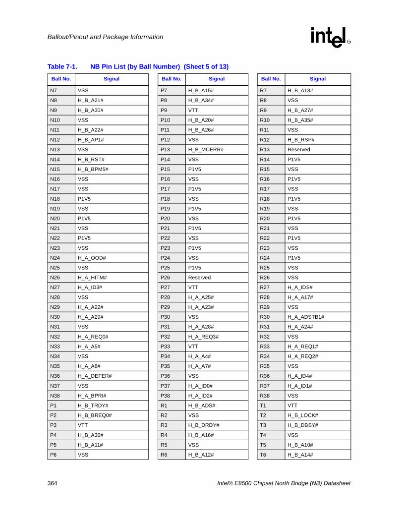
364 Intel® E8500 Chipset North Bridge (NB) Datasheet
Ballout/Pinout and Package Information
N7 VSS P7 H_B_A15# R7 H_B_A13#
N8 H_B_A21# P8 H_B_A34# R8 VSS
N9 H_B_A30# P9 VTT R9 H_B_A27#
N10 VSS P10 H_B_A20# R10 H_B_A35#
N11 H_B_A22# P11 H_B_A26# R11 VSS
N12 H_B_AP1# P12 VSS R12 H_B_RSP#
N13 VSS P13 H_B_MCERR# R13 Reserved
N14 H_B_RST# P14 VSS R14 P1V5
N15 H_B_BPM5# P15 P1V5 R15 VSS
N16 VSS P16 VSS R16 P1V5
N17 VSS P17 P1V5 R17 VSS
N18 P1V5 P18 VSS R18 P1V5
N19 VSS P19 P1V5 R19 VSS
N20 P1V5 P20 VSS R20 P1V5
N21 VSS P21 P1V5 R21 VSS
N22 P1V5 P22 VSS R22 P1V5
N23 VSS P23 P1V5 R23 VSS
N24 H_A_OOD# P24 VSS R24 P1V5
N25 VSS P25 P1V5 R25 VSS
N26 H_A_HITM# P26 Reserved R26 VSS
N27 H_A_ID3# P27 VTT R27 H_A_IDS#
N28 VSS P28 H_A_A25# R28 H_A_A17#
N29 H_A_A22# P29 H_A_A23# R29 VSS
N30 H_A_A29# P30 VSS R30 H_A_ADSTB1#
N31 VSS P31 H_A_A28# R31 H_A_A24#
N32 H_A_REQ0# P32 H_A_REQ3# R32 VSS
N33 H_A_A5# P33 VTT R33 H_A_REQ1#
N34 VSS P34 H_A_A4# R34 H_A_REQ2#
N35 H_A_A6# P35 H_A_A7# R35 VSS
N36 H_A_DEFER# P36 VSS R36 H_A_ID4#
N37 VSS P37 H_A_ID0# R37 H_A_ID1#
N38 H_A_BPRI# P38 H_A_ID2# R38 VSS
P1 H_B_TRDY# R1 H_B_ADS# T1 VTT
P2 H_B_BREQ0# R2 VSS T2 H_B_LOCK#
P3 VTT R3 H_B_DRDY# T3 H_B_DBSY#
P4 H_B_A36# R4 H_B_A16# T4 VSS
P5 H_B_A11# R5 VSS T5 H_B_A10#
P6 VSS R6 H_B_A12# T6 H_B_A14#
Table 7-1. NB Pin List (by Ball Number) (Sheet 5 of 13)
Ball No. Signal Ball No. Signal Ball No. Signal
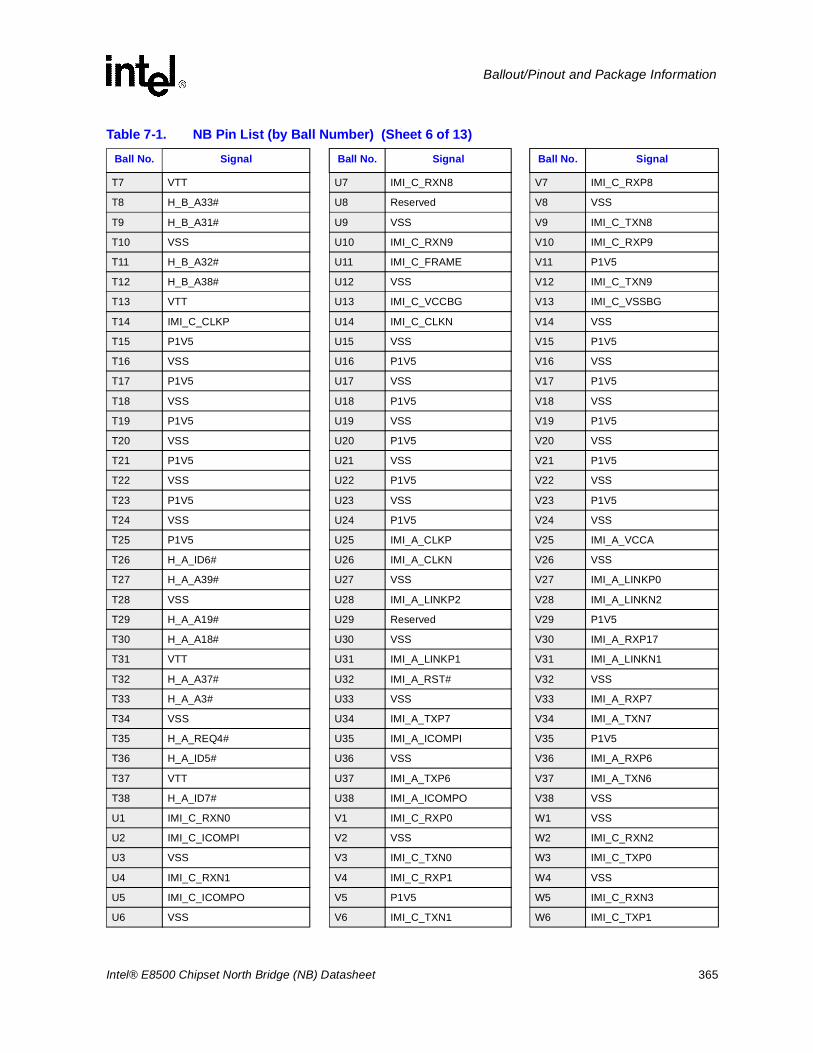
Intel® E8500 Chipset North Bridge (NB) Datasheet 365
Ballout/Pinout and Package Information
T7 VTT U7 IMI_C_RXN8 V7 IMI_C_RXP8
T8 H_B_A33# U8 Reserved V8 VSS
T9 H_B_A31# U9 VSS V9 IMI_C_TXN8
T10 VSS U10 IMI_C_RXN9 V10 IMI_C_RXP9
T11 H_B_A32# U11 IMI_C_FRAME V11 P1V5
T12 H_B_A38# U12 VSS V12 IMI_C_TXN9
T13 VTT U13 IMI_C_VCCBG V13 IMI_C_VSSBG
T14 IMI_C_CLKP U14 IMI_C_CLKN V14 VSS
T15 P1V5 U15 VSS V15 P1V5
T16 VSS U16 P1V5 V16 VSS
T17 P1V5 U17 VSS V17 P1V5
T18 VSS U18 P1V5 V18 VSS
T19 P1V5 U19 VSS V19 P1V5
T20 VSS U20 P1V5 V20 VSS
T21 P1V5 U21 VSS V21 P1V5
T22 VSS U22 P1V5 V22 VSS
T23 P1V5 U23 VSS V23 P1V5
T24 VSS U24 P1V5 V24 VSS
T25 P1V5 U25 IMI_A_CLKP V25 IMI_A_VCCA
T26 H_A_ID6# U26 IMI_A_CLKN V26 VSS
T27 H_A_A39# U27 VSS V27 IMI_A_LINKP0
T28 VSS U28 IMI_A_LINKP2 V28 IMI_A_LINKN2
T29 H_A_A19# U29 Reserved V29 P1V5
T30 H_A_A18# U30 VSS V30 IMI_A_RXP17
T31 VTT U31 IMI_A_LINKP1 V31 IMI_A_LINKN1
T32 H_A_A37# U32 IMI_A_RST# V32 VSS
T33 H_A_A3# U33 VSS V33 IMI_A_RXP7
T34 VSS U34 IMI_A_TXP7 V34 IMI_A_TXN7
T35 H_A_REQ4# U35 IMI_A_ICOMPI V35 P1V5
T36 H_A_ID5# U36 VSS V36 IMI_A_RXP6
T37 VTT U37 IMI_A_TXP6 V37 IMI_A_TXN6
T38 H_A_ID7# U38 IMI_A_ICOMPO V38 VSS
U1 IMI_C_RXN0 V1 IMI_C_RXP0 W1 VSS
U2 IMI_C_ICOMPI V2 VSS W2 IMI_C_RXN2
U3 VSS V3 IMI_C_TXN0 W3 IMI_C_TXP0
U4 IMI_C_RXN1 V4 IMI_C_RXP1 W4 VSS
U5 IMI_C_ICOMPO V5 P1V5 W5 IMI_C_RXN3
U6 VSS V6 IMI_C_TXN1 W6 IMI_C_TXP1
Table 7-1. NB Pin List (by Ball Number) (Sheet 6 of 13)
Ball No. Signal Ball No. Signal Ball No. Signal
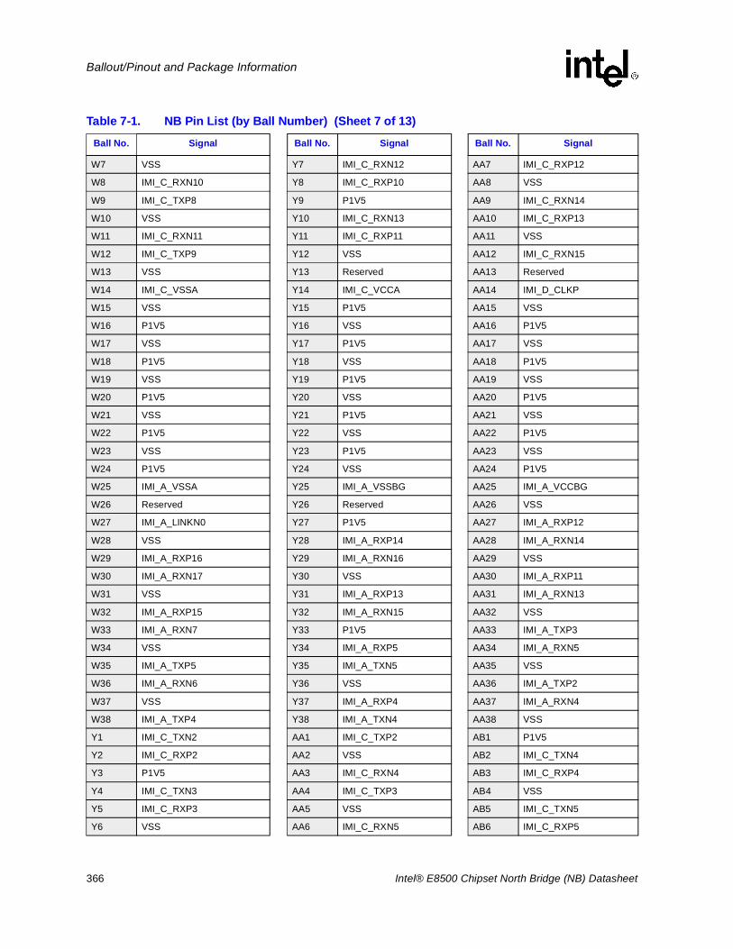
366 Intel® E8500 Chipset North Bridge (NB) Datasheet
Ballout/Pinout and Package Information
W7 VSS Y7 IMI_C_RXN12 AA7 IMI_C_RXP12
W8 IMI_C_RXN10 Y8 IMI_C_RXP10 AA8 VSS
W9 IMI_C_TXP8 Y9 P1V5 AA9 IMI_C_RXN14
W10 VSS Y10 IMI_C_RXN13 AA10 IMI_C_RXP13
W11 IMI_C_RXN11 Y11 IMI_C_RXP11 AA11 VSS
W12 IMI_C_TXP9 Y12 VSS AA12 IMI_C_RXN15
W13 VSS Y13 Reserved AA13 Reserved
W14 IMI_C_VSSA Y14 IMI_C_VCCA AA14 IMI_D_CLKP
W15 VSS Y15 P1V5 AA15 VSS
W16 P1V5 Y16 VSS AA16 P1V5
W17 VSS Y17 P1V5 AA17 VSS
W18 P1V5 Y18 VSS AA18 P1V5
W19 VSS Y19 P1V5 AA19 VSS
W20 P1V5 Y20 VSS AA20 P1V5
W21 VSS Y21 P1V5 AA21 VSS
W22 P1V5 Y22 VSS AA22 P1V5
W23 VSS Y23 P1V5 AA23 VSS
W24 P1V5 Y24 VSS AA24 P1V5
W25 IMI_A_VSSA Y25 IMI_A_VSSBG AA25 IMI_A_VCCBG
W26 Reserved Y26 Reserved AA26 VSS
W27 IMI_A_LINKN0 Y27 P1V5 AA27 IMI_A_RXP12
W28 VSS Y28 IMI_A_RXP14 AA28 IMI_A_RXN14
W29 IMI_A_RXP16 Y29 IMI_A_RXN16 AA29 VSS
W30 IMI_A_RXN17 Y30 VSS AA30 IMI_A_RXP11
W31 VSS Y31 IMI_A_RXP13 AA31 IMI_A_RXN13
W32 IMI_A_RXP15 Y32 IMI_A_RXN15 AA32 VSS
W33 IMI_A_RXN7 Y33 P1V5 AA33 IMI_A_TXP3
W34 VSS Y34 IMI_A_RXP5 AA34 IMI_A_RXN5
W35 IMI_A_TXP5 Y35 IMI_A_TXN5 AA35 VSS
W36 IMI_A_RXN6 Y36 VSS AA36 IMI_A_TXP2
W37 VSS Y37 IMI_A_RXP4 AA37 IMI_A_RXN4
W38 IMI_A_TXP4 Y38 IMI_A_TXN4 AA38 VSS
Y1 IMI_C_TXN2 AA1 IMI_C_TXP2 AB1 P1V5
Y2 IMI_C_RXP2 AA2 VSS AB2 IMI_C_TXN4
Y3 P1V5 AA3 IMI_C_RXN4 AB3 IMI_C_RXP4
Y4 IMI_C_TXN3 AA4 IMI_C_TXP3 AB4 VSS
Y5 IMI_C_RXP3 AA5 VSS AB5 IMI_C_TXN5
Y6 VSS AA6 IMI_C_RXN5 AB6 IMI_C_RXP5
Table 7-1. NB Pin List (by Ball Number) (Sheet 7 of 13)
Ball No. Signal Ball No. Signal Ball No. Signal
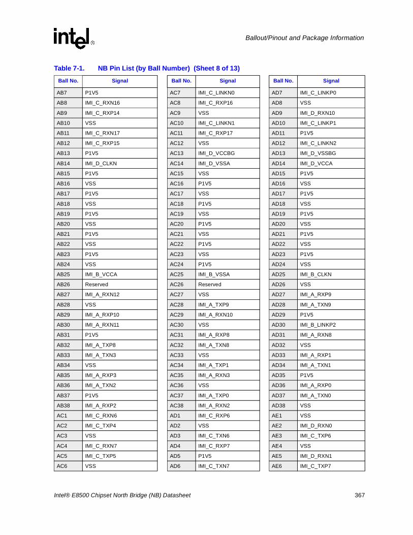
Intel® E8500 Chipset North Bridge (NB) Datasheet 367
Ballout/Pinout and Package Information
AB7 P1V5 AC7 IMI_C_LINKN0 AD7 IMI_C_LINKP0
AB8 IMI_C_RXN16 AC8 IMI_C_RXP16 AD8 VSS
AB9 IMI_C_RXP14 AC9 VSS AD9 IMI_D_RXN10
AB10 VSS AC10 IMI_C_LINKN1 AD10 IMI_C_LINKP1
AB11 IMI_C_RXN17 AC11 IMI_C_RXP17 AD11 P1V5
AB12 IMI_C_RXP15 AC12 VSS AD12 IMI_C_LINKN2
AB13 P1V5 AC13 IMI_D_VCCBG AD13 IMI_D_VSSBG
AB14 IMI_D_CLKN AC14 IMI_D_VSSA AD14 IMI_D_VCCA
AB15 P1V5 AC15 VSS AD15 P1V5
AB16 VSS AC16 P1V5 AD16 VSS
AB17 P1V5 AC17 VSS AD17 P1V5
AB18 VSS AC18 P1V5 AD18 VSS
AB19 P1V5 AC19 VSS AD19 P1V5
AB20 VSS AC20 P1V5 AD20 VSS
AB21 P1V5 AC21 VSS AD21 P1V5
AB22 VSS AC22 P1V5 AD22 VSS
AB23 P1V5 AC23 VSS AD23 P1V5
AB24 VSS AC24 P1V5 AD24 VSS
AB25 IMI_B_VCCA AC25 IMI_B_VSSA AD25 IMI_B_CLKN
AB26 Reserved AC26 Reserved AD26 VSS
AB27 IMI_A_RXN12 AC27 VSS AD27 IMI_A_RXP9
AB28 VSS AC28 IMI_A_TXP9 AD28 IMI_A_TXN9
AB29 IMI_A_RXP10 AC29 IMI_A_RXN10 AD29 P1V5
AB30 IMI_A_RXN11 AC30 VSS AD30 IMI_B_LINKP2
AB31 P1V5 AC31 IMI_A_RXP8 AD31 IMI_A_RXN8
AB32 IMI_A_TXP8 AC32 IMI_A_TXN8 AD32 VSS
AB33 IMI_A_TXN3 AC33 VSS AD33 IMI_A_RXP1
AB34 VSS AC34 IMI_A_TXP1 AD34 IMI_A_TXN1
AB35 IMI_A_RXP3 AC35 IMI_A_RXN3 AD35 P1V5
AB36 IMI_A_TXN2 AC36 VSS AD36 IMI_A_RXP0
AB37 P1V5 AC37 IMI_A_TXP0 AD37 IMI_A_TXN0
AB38 IMI_A_RXP2 AC38 IMI_A_RXN2 AD38 VSS
AC1 IMI_C_RXN6 AD1 IMI_C_RXP6 AE1 VSS
AC2 IMI_C_TXP4 AD2 VSS AE2 IMI_D_RXN0
AC3 VSS AD3 IMI_C_TXN6 AE3 IMI_C_TXP6
AC4 IMI_C_RXN7 AD4 IMI_C_RXP7 AE4 VSS
AC5 IMI_C_TXP5 AD5 P1V5 AE5 IMI_D_RXN1
AC6 VSS AD6 IMI_C_TXN7 AE6 IMI_C_TXP7
Table 7-1. NB Pin List (by Ball Number) (Sheet 8 of 13)
Ball No. Signal Ball No. Signal Ball No. Signal
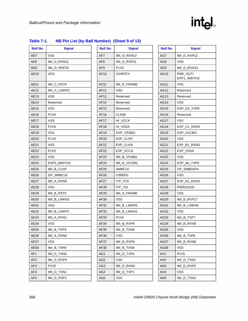
368 Intel® E8500 Chipset North Bridge (NB) Datasheet
Ballout/Pinout and Package Information
AE7 VSS AF7 IMI_D_RXN12 AG7 IMI_D_RXP12
AE8 IMI_D_RXN11 AF8 IMI_D_RXP11 AG8 VSS
AE9 IMI_D_RXP10 AF9 P1V5 AG9 IMI_D_RXN13
AE10 VSS AF10 ICHRST# AG10 PME_OUT/EXP1_WIDTH2
AE11 IMI_C_RST# AF11 IMI_D_FRAME AG11 VSS
AE12 IMI_C_LINKP2 AF12 VSS AG12 Reserved
AE13 VSS AF13 Reserved AG13 Reserved
AE14 Reserved AF14 Reserved AG14 VSS
AE15 VSS AF15 Reserved AG15 EXP_C0_TXP0
AE16 P1V5 AF16 CLK66 AG16 Reserved
AE17 VSS AF17 HI_VCCA AG17 VSS
AE18 P1V5 AF18 HI_VSSA AG18 EXP_C1_RXN3
AE19 VSS AF19 EXP_VSSBG AG19 EXP_VCCBG
AE20 P1V5 AF20 EXP_CLKP AG20 VSS
AE21 VSS AF21 EXP_CLKN AG21 EXP_B1_RXN3
AE22 P1V5 AF22 EXP_VCCA AG22 EXP_VSSA
AE23 VSS AF23 IMI_B_VSSBG AG23 VSS
AE24 EXP0_WIDTH0 AF24 IMI_B_VCCBG AG24 EXP_A0_TXP0
AE25 IMI_B_CLKP AF25 SMBCLK AG25 GP_SMBDATA
AE26 GP_SMBCLK AF26 V3REF0 AG26 VSS
AE27 IMI_A_RXN9 AF27 ITP_TCK AG27 EXP_A1_RXN3
AE28 VSS AF28 ITP_TDI AG28 PWRGOOD
AE29 IMI_B_RST# AF29 IMI_A_FRAME AG29 VSS
AE30 IMI_B_LINKN2 AF30 VSS AG30 IMI_B_RXP17
AE31 VSS AF31 IMI_B_LINKP0 AG31 IMI_B_LINKN0
AE32 IMI_B_LINKP1 AF32 IMI_B_LINKN1 AG32 VSS
AE33 IMI_A_RXN1 AF33 P1V5 AG33 IMI_B_TXP7
AE34 VSS AF34 IMI_B_RXP9 AG34 IMI_B_RXN9
AE35 IMI_B_TXP9 AF35 IMI_B_TXN9 AG35 VSS
AE36 IMI_A_RXN0 AF36 VSS AG36 IMI_B_TXP6
AE37 VSS AF37 IMI_B_RXP8 AG37 IMI_B_RXN8
AE38 IMI_B_TXP8 AF38 IMI_B_TXN8 AG38 VSS
AF1 IMI_D_TXN0 AG1 IMI_D_TXP0 AH1 P1V5
AF2 IMI_D_RXP0 AG2 VSS AH2 IMI_D_TXN2
AF3 P1V5 AG3 IMI_D_RXN2 AH3 IMI_D_RXP2
AF4 IMI_D_TXN1 AG4 IMI_D_TXP1 AH4 VSS
AF5 IMI_D_RXP1 AG5 VSS AH5 IMI_D_TXN3
Table 7-1. NB Pin List (by Ball Number) (Sheet 9 of 13)
Ball No. Signal Ball No. Signal Ball No. Signal
Intel® E8500 Chipset North Bridge (NB) Datasheet 369
Ballout/Pinout and Package Information
AF6 VSS AG6 IMI_D_RXN3 AH6 IMI_D_RXP3
AH7 P1V5 AJ7 IMI_D_RXN15 AK7 IMI_D_RXP15
AH8 IMI_D_RXN14 AJ8 IMI_D_RXP14 AK8 VSS
AH9 IMI_D_RXP13 AJ9 VSS AK9 IMI_D_RXN16
AH10 VSS AJ10 V3REF1 AK10 Reserved
AH11 EXP_HPINT/EXP1_WIDTH1 AJ11 Reserved AK11 P1V5
AH12 IMI_HPINT AJ12 VSS AK12 EXP1_SPE C10A
AH13 P1V5 AJ13 EXP_D_RXP0 AK13 EXP_D_RXN0
AH14 EXP_D_TXP0 AJ14 EXP_D_TXN0 AK14 VSS
AH15 EXP_C0_TXN0 AJ15 VSS AK15 EXP_C0_RXP1
AH16 VSS AJ16 EXP_C0_TXP1 AK16 EXP_C0_TXN1
AH17 EXP_C0_RXP0 AJ17 EXP_C0_RXN0 AK17 P1V5
AH18 EXP_C1_RXP3 AJ18 VSS AK18 EXP_C1_TXN3
AH19 P1V5 AJ19 EXP_B0_RXP0 AK19 EXP_B0_RXN0
AH20 EXP_B0_TXP0 AJ20 EXP_B0_TXN0 AK20 VSS
AH21 EXP_B1_RXP3 AJ21 VSS AK21 EXP_B0_TXP1
AH22 VSS AJ22 EXP_B1_TXN3 AK22 EXP_B1_TXP3
AH23 EXP_A0_RXP0 AJ23 EXP_A0_RXN0 AK23 P1V5
AH24 EXP_A0_TXN0 AJ24 VSS AK24 EXP_A0_RXP1
AH25 P1V5 AJ25 EXP_A0_TXP1 AK25 EXP_A0_TXN1
AH26 EXP_A1_TXN3 AJ26 EXP_A1_TXP3 AK26 VSS
AH27 EXP_A1_RXP3 AJ27 VSS AK27 EXP_A1_RXN2
AH28 ITP_TMS AJ28 Reserved AK28 ERR0#
AH29 RSTIN# AJ29 Reserved AK29 P1V5
AH30 IMI_B_RXN17 AJ30 VSS AK30 IMI_B_RXP14
AH31 P1V5 AJ31 IMI_B_RXP15 AK31 IMI_B_RXN15
AH32 IMI_B_RXP16 AJ32 IMI_B_RXN16 AK32 VSS
AH33 IMI_B_TXN7 AJ33 VSS AK33 IMI_B_RXP5
AH34 VSS AJ34 IMI_B_TXP5 AK34 IMI_B_TXN5
AH35 IMI_B_RXP7 AJ35 IMI_B_RXN7 AK35 P1V5
AH36 IMI_B_TXN6 AJ36 VSS AK36 IMI_B_RXP4
AH37 P1V5 AJ37 IMI_B_TXP4 AK37 IMI_B_TXN4
AH38 IMI_B_RXP6 AJ38 IMI_B_RXN6 AK38 VSS
AJ1 IMI_D_RXN4 AK1 IMI_D_RXP4 AL1 VSS
AJ2 IMI_D_TXP2 AK2 VSS AL2 IMI_D_RXN6
AJ3 VSS AK3 IMI_D_TXN4 AL3 IMI_D_TXP4
AJ4 IMI_D_RXN5 AK4 IMI_D_RXP5 AL4 VSS
AJ5 IMI_D_TXP3 AK5 P1V5 AL5 IMI_D_RXN7
Table 7-1. NB Pin List (by Ball Number) (Sheet 10 of 13)
Ball No. Signal Ball No. Signal Ball No. Signal

370 Intel® E8500 Chipset North Bridge (NB) Datasheet
Ballout/Pinout and Package Information
AJ6 VSS AK6 IMI_D_TXN5 AL6 IMI_D_TXP5
AL7 VSS AM7 IMI_D_LINKN0 AN7 IMI_D_LINKP0
AL8 IMI_D_RXN17 AM8 IMI_D_RXP17 AN8 VSS
AL9 IMI_D_RXP16 AM9 P1V5 AN9 IMI_D_LINKN1
AL10 VSS AM10 Reserved AN10 Reserved
AL11 Reserved AM11 Reserved AN11 VSS
AL12 Reserved AM12 VSS AN12 EXP_D_TXP2
AL13 VSS AM13 EXP_D_RXP1 AN13 EXP_D_RXN1
AL14 EXP_D_TXP1 AM14 EXP_D_TXN1 AN14 VSS
AL15 EXP_C0_RXN1 AM15 P1V5 AN15 EXP_C0_RXP2
AL16 VSS AM16 EXP_C0_TXP2 AN16 EXP_C0_TXN2
AL17 EXP_C1_RXN2 AM17 EXP_C1_RXP2 AN17 VSS
AL18 EXP_C1_TXP3 AM18 VSS AN18 EXP_C1_TXN2
AL19 VSS AM19 EXP_B0_TXP2 AN19 EXP_B0_TXN2
AL20 EXP_B0_RXP1 AM20 EXP_B0_RXN1 AN20 VSS
AL21 EXP_B0_TXN1 AM21 P1V5 AN21 EXP_B1_RXN1
AL22 VSS AM22 EXP_B1_TXN2 AN22 EXP_B1_TXP2
AL23 EXP_B1_RXN2 AM23 EXP_B1_RXP2 AN23 VSS
AL24 EXP_A0_RXN1 AM24 VSS AN24 EXP_A0_RXP2
AL25 VSS AM25 EXP_A0_TXP2 AN25 EXP_A0_TXN2
AL26 EXP_A1_TXN2 AM26 EXP_A1_TXP2 AN26 VSS
AL27 EXP_A1_RXP2 AM27 P1V5 AN27 EXP_A1_RXN1
AL28 VSS AM28 EXP0_SPEC10A AN28 XDP_ODTCRES
AL29 ERR1# AM29 ERR2# AN29 VSS
AL30 IMI_B_RXN14 AM30 VSS AN30 IMI_B_RXP11
AL31 VSS AM31 IMI_B_RXP12 AN31 IMI_B_RXN12
AL32 IMI_B_RXP13 AM32 IMI_B_RXN13 AN32 VSS
AL33 IMI_B_RXN5 AM33 P1V5 AN33 IMI_B_TXP1
AL34 VSS AM34 IMI_B_RXP3 AN34 IMI_B_RXN3
AL35 IMI_B_TXP3 AM35 IMI_B_TXN3 AN35 VSS
AL36 IMI_B_RXN4 AM36 VSS AN36 IMI_B_TXP0
AL37 VSS AM37 IMI_B_RXP2 AN37 IMI_B_RXN2
AL38 IMI_B_TXP2 AM38 IMI_B_TXN2 AN38 VSS
AM1 IMI_D_TXN6 AN1 IMI_D_TXP6 AP1 P1V5
AM2 IMI_D_RXP6 AN2 VSS AP2 IMI_D_TXN8
AM3 P1V5 AN3 IMI_D_RXN8 AP3 IMI_D_RXP8
AM4 IMI_D_TXN7 AN4 IMI_D_TXP7 AP4 VSS
AM5 IMI_D_RXP7 AN5 VSS AP5 IMI_D_TXN9
Table 7-1. NB Pin List (by Ball Number) (Sheet 11 of 13)
Ball No. Signal Ball No. Signal Ball No. Signal
Intel® E8500 Chipset North Bridge (NB) Datasheet 371
Ballout/Pinout and Package Information
AM6 VSS AN6 IMI_D_RXN9 AP6 IMI_D_RXP9
AP7 P1V5 AR7 IMI_D_RST# AT7 HI5
AP8 IMI_D_LINKN2 AR8 IMI_D_LINKP2 AT8 VSS
AP9 IMI_D_LINKP1 AR9 VSS AT9 HIRCOMP
AP10 VSS AR10 Reserved AT10 Reserved
AP11 Reserved AR11 Reserved AT11 P1V5
AP12 EXP_D_TXN2 AR12 VSS AT12 EXP_D_TXP3
AP13 P1V5 AR13 Reserved AT13 EXP_D_TXN3
AP14 EXP_D_RXP2 AR14 EXP_D_RXN2 AT14 VSS
AP15 EXP_C0_RXN2 AR15 VSS AT15 EXP_C0_RXP3
AP16 VSS AR16 EXP_ICOMPI AT16 EXP_C0_RXN3
AP17 EXP_C1_TXN1 AR17 EXP_C1_TXP1 AT17 P1V5
AP18 EXP_C1_TXP2 AR18 VSS AT18 Reserved
AP19 P1V5 AR19 EXP_C1_RXN1 AT19 EXP_C1_RXP1
AP20 EXP_B0_RXP2 AR20 EXP_B0_RXN2 AT20 VSS
AP21 EXP_B1_RXP1 AR21 VSS AT21 EXP_B1_TXP0
AP22 VSS AR22 EXP_RCOMP AT22 EXP_B1_TXN0
AP23 EXP_B1_TXN1 AR23 EXP_B1_TXP1 AT23 P1V5
AP24 EXP_A0_RXN2 AR24 VSS AT24 EXP_A0_RXP3
AP25 P1V5 AR25 ITP_TRST# AT25 EXP_A0_RXN3
AP26 EXP_A1_TXN1 AR26 EXP_A1_TXP1 AT26 VSS
AP27 EXP_A1_RXP1 AR27 VSS AT27 EXP0_WIDTH1
AP28 VSS AR28 SMBDATA AT28 XDP_D15#
AP29 XDP_SLWCRES AR29 XDP_CRES AT29 P1V5
AP30 IMI_B_RXN11 AR30 VSS AT30 XDP_D13#
AP31 P1V5 AR31 IMI_B_FRAME AT31 XDP_D12#
AP32 IMI_B_RXP10 AR32 IMI_B_RXN10 AT32 VSS
AP33 IMI_B_TXN1 AR33 VSS AT33 XDP_D10#
AP34 VSS AR34 IMI_B_ICOMPI AT34 XDP_D9#
AP35 IMI_B_RXP1 AR35 IMI_B_RXN1 AT35 VSS
AP36 IMI_B_TXN0 AR36 VSS AT36 XDP_DSTBP
AP37 P1V5 AR37 IMI_B_ICOMPO AT37 XDP_DSTBN
AP38 IMI_B_RXP0 AR38 IMI_B_RXN0 AT38 VSS
AR1 IMI_D_ICOMPI AT1 VSS AU2 VSS
AR2 IMI_D_TXP8 AT2 HI11 AU3 HI1
AR3 VSS AT3 HI0 AU4 HI2
AR4 IMI_D_ICOMPO AT4 HI3 AU5 HI8
AR5 IMI_D_TXP9 AT5 P1V5 AU6 HI9
Table 7-1. NB Pin List (by Ball Number) (Sheet 12 of 13)
Ball No. Signal Ball No. Signal Ball No. Signal
372 Intel® E8500 Chipset North Bridge (NB) Datasheet
Ballout/Pinout and Package Information
AR6 VSS AT6 HI10 AU7 VSS
AU8 HI7 AU30 XDP_D5# AV17 EXP_C1_TXN0
AU9 HIVSWING AU31 P1V5 AV18 VSS
AU10 VSS AU32 XDP_D11# AV19 EXP_B0_TXP3
AU11 Reserved AU33 XDP_D2# AV20 EXP_B0_TXN3
AU12 Reserved AU34 P1V5 AV21 P1V5
AU13 VSS AU35 XDP_D8# AV22 EXP_B1_RXP0
AU14 EXP_C0_TXP3 AU36 XDP_RDY# AV23 EXP_B1_RXN0
AU15 EXP_C0_TXN3 AU37 VSS AV24 VSS
AU16 VSS AV3 VSS AV25 EXP_A1_TXP0
AU17 EXP_C1_RXP0 AV4 HI_STBS AV26 EXP_A1_TXN0
AU18 EXP_C1_RXN0 AV5 HI_STBF AV27 P1V5
AU19 VSS AV6 VSS AV28 XDP_D7#
AU20 EXP_B0_RXP3 AV7 HI4 AV29 XDP_D6#
AU21 EXP_B0_RXN3 AV8 HI6 AV30 VSS
AU22 VSS AV9 P1V5 AV31 XDP_D4#
AU23 EXP_A0_TXP3 AV10 HIVREF AV32 XDP_D3#
AU24 EXP_A0_TXN3 AV11 Reserved AV33 VSS
AU25 VSS AV12 VSS AV34 XDP_D1#
AU26 EXP_A1_RXP0 AV13 EXP_D_RXP3 AV35 XDP_D0#
AU27 EXP_A1_RXN0 AV14 EXP_D_RXN3 AV36 VSS
AU28 ITP_TDO AV15 P1V5
AU29 XDP_D14# AV16 EXP_C1_TXP0
Table 7-1. NB Pin List (by Ball Number) (Sheet 13 of 13)
Ball No. Signal Ball No. Signal Ball No. Signal
Intel® E8500 Chipset North Bridge (NB) Datasheet 373
Ballout/Pinout and Package Information
Table 7-2. NB Pin List (by Signal Name) (Sheet 1 of 13)
Ball No. Signal Ball No. Signal Ball No. Signal
AF16 CLK66 AR20 EXP_B0_RXN2 AH15 EXP_C0_TXN0
AK28 ERR0# AU21 EXP_B0_RXN3 AK16 EXP_C0_TXN1
AL29 ERR1# AJ19 EXP_B0_RXP0 AN16 EXP_C0_TXN2
AM29 ERR2# AL20 EXP_B0_RXP1 AU15 EXP_C0_TXN3
AJ23 EXP_A0_RXN0 AP20 EXP_B0_RXP2 AG15 EXP_C0_TXP0
AL24 EXP_A0_RXN1 AU20 EXP_B0_RXP3 AJ16 EXP_C0_TXP1
AP24 EXP_A0_RXN2 AJ20 EXP_B0_TXN0 AM16 EXP_C0_TXP2
AT25 EXP_A0_RXN3 AL21 EXP_B0_TXN1 AU14 EXP_C0_TXP3
AH23 EXP_A0_RXP0 AN19 EXP_B0_TXN2 AU18 EXP_C1_RXN0
AK24 EXP_A0_RXP1 AV20 EXP_B0_TXN3 AR19 EXP_C1_RXN1
AN24 EXP_A0_RXP2 AH20 EXP_B0_TXP0 AL17 EXP_C1_RXN2
AT24 EXP_A0_RXP3 AK21 EXP_B0_TXP1 AG18 EXP_C1_RXN3
AH24 EXP_A0_TXN0 AM19 EXP_B0_TXP2 AU17 EXP_C1_RXP0
AK25 EXP_A0_TXN1 AV19 EXP_B0_TXP3 AT19 EXP_C1_RXP1
AN25 EXP_A0_TXN2 AV23 EXP_B1_RXN0 AM17 EXP_C1_RXP2
AU24 EXP_A0_TXN3 AN21 EXP_B1_RXN1 AH18 EXP_C1_RXP3
AG24 EXP_A0_TXP0 AL23 EXP_B1_RXN2 AV17 EXP_C1_TXN0
AJ25 EXP_A0_TXP1 AG21 EXP_B1_RXN3 AP17 EXP_C1_TXN1
AM25 EXP_A0_TXP2 AV22 EXP_B1_RXP0 AN18 EXP_C1_TXN2
AU23 EXP_A0_TXP3 AP21 EXP_B1_RXP1 AK18 EXP_C1_TXN3
AU27 EXP_A1_RXN0 AM23 EXP_B1_RXP2 AV16 EXP_C1_TXP0
AN27 EXP_A1_RXN1 AH21 EXP_B1_RXP3 AR17 EXP_C1_TXP1
AK27 EXP_A1_RXN2 AT22 EXP_B1_TXN0 AP18 EXP_C1_TXP2
AG27 EXP_A1_RXN3 AP23 EXP_B1_TXN1 AL18 EXP_C1_TXP3
AU26 EXP_A1_RXP0 AM22 EXP_B1_TXN2 AF21 EXP_CLKN
AP27 EXP_A1_RXP1 AJ22 EXP_B1_TXN3 AF20 EXP_CLKP
AL27 EXP_A1_RXP2 AT21 EXP_B1_TXP0 AK13 EXP_D_RXN0
AH27 EXP_A1_RXP3 AR23 EXP_B1_TXP1 AN13 EXP_D_RXN1
AV26 EXP_A1_TXN0 AN22 EXP_B1_TXP2 AR14 EXP_D_RXN2
AP26 EXP_A1_TXN1 AK22 EXP_B1_TXP3 AV14 EXP_D_RXN3
AL26 EXP_A1_TXN2 AJ17 EXP_C0_RXN0 AJ13 EXP_D_RXP0
AH26 EXP_A1_TXN3 AL15 EXP_C0_RXN1 AM13 EXP_D_RXP1
AV25 EXP_A1_TXP0 AP15 EXP_C0_RXN2 AP14 EXP_D_RXP2
AR26 EXP_A1_TXP1 AT16 EXP_C0_RXN3 AV13 EXP_D_RXP3
AM26 EXP_A1_TXP2 AH17 EXP_C0_RXP0 AJ14 EXP_D_TXN0
AJ26 EXP_A1_TXP3 AK15 EXP_C0_RXP1 AM14 EXP_D_TXN1
AK19 EXP_B0_RXN0 AN15 EXP_C0_RXP2 AP12 EXP_D_TXN2
AM20 EXP_B0_RXN1 AT15 EXP_C0_RXP3 AT13 EXP_D_TXN3
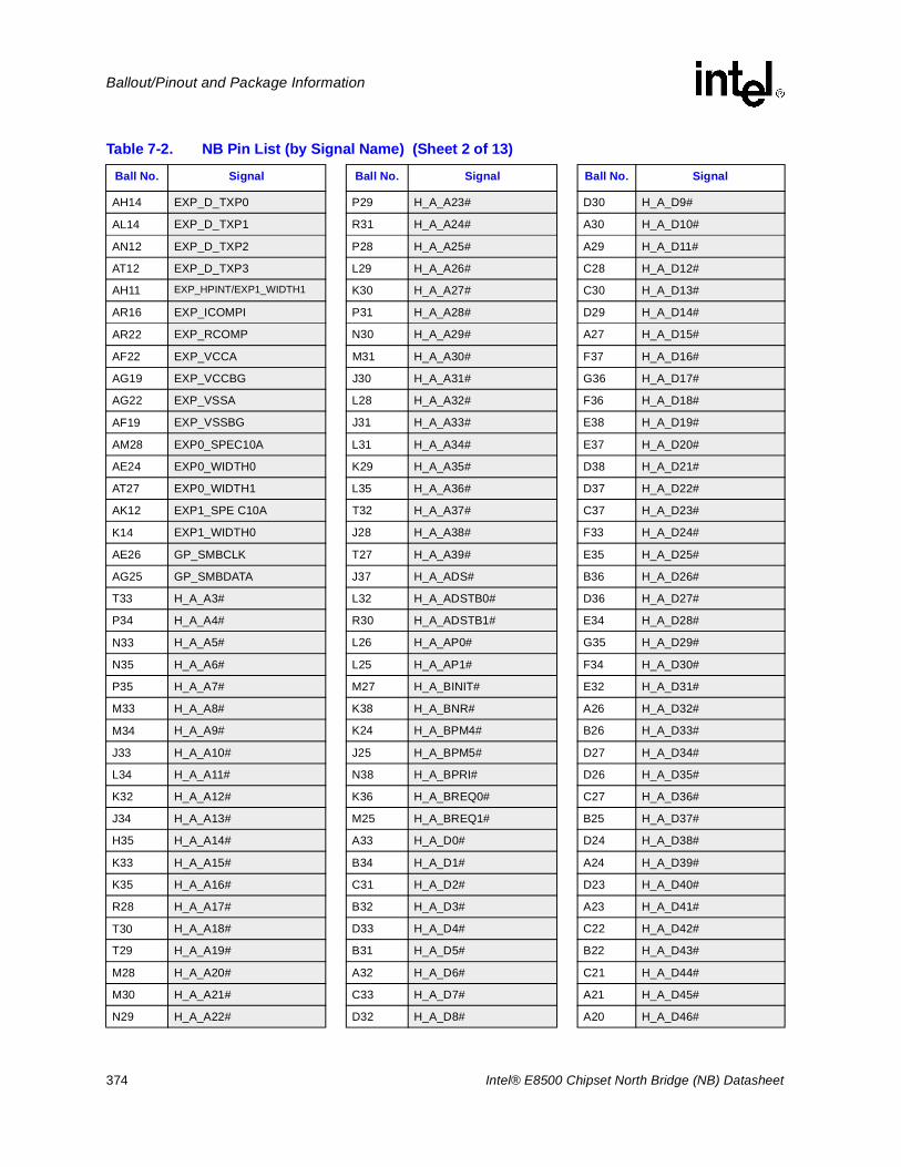
374 Intel® E8500 Chipset North Bridge (NB) Datasheet
Ballout/Pinout and Package Information
AH14 EXP_D_TXP0 P29 H_A_A23# D30 H_A_D9#
AL14 EXP_D_TXP1 R31 H_A_A24# A30 H_A_D10#
AN12 EXP_D_TXP2 P28 H_A_A25# A29 H_A_D11#
AT12 EXP_D_TXP3 L29 H_A_A26# C28 H_A_D12#
AH11 EXP_HPINT/EXP1_WIDTH1 K30 H_A_A27# C30 H_A_D13#
AR16 EXP_ICOMPI P31 H_A_A28# D29 H_A_D14#
AR22 EXP_RCOMP N30 H_A_A29# A27 H_A_D15#
AF22 EXP_VCCA M31 H_A_A30# F37 H_A_D16#
AG19 EXP_VCCBG J30 H_A_A31# G36 H_A_D17#
AG22 EXP_VSSA L28 H_A_A32# F36 H_A_D18#
AF19 EXP_VSSBG J31 H_A_A33# E38 H_A_D19#
AM28 EXP0_SPEC10A L31 H_A_A34# E37 H_A_D20#
AE24 EXP0_WIDTH0 K29 H_A_A35# D38 H_A_D21#
AT27 EXP0_WIDTH1 L35 H_A_A36# D37 H_A_D22#
AK12 EXP1_SPE C10A T32 H_A_A37# C37 H_A_D23#
K14 EXP1_WIDTH0 J28 H_A_A38# F33 H_A_D24#
AE26 GP_SMBCLK T27 H_A_A39# E35 H_A_D25#
AG25 GP_SMBDATA J37 H_A_ADS# B36 H_A_D26#
T33 H_A_A3# L32 H_A_ADSTB0# D36 H_A_D27#
P34 H_A_A4# R30 H_A_ADSTB1# E34 H_A_D28#
N33 H_A_A5# L26 H_A_AP0# G35 H_A_D29#
N35 H_A_A6# L25 H_A_AP1# F34 H_A_D30#
P35 H_A_A7# M27 H_A_BINIT# E32 H_A_D31#
M33 H_A_A8# K38 H_A_BNR# A26 H_A_D32#
M34 H_A_A9# K24 H_A_BPM4# B26 H_A_D33#
J33 H_A_A10# J25 H_A_BPM5# D27 H_A_D34#
L34 H_A_A11# N38 H_A_BPRI# D26 H_A_D35#
K32 H_A_A12# K36 H_A_BREQ0# C27 H_A_D36#
J34 H_A_A13# M25 H_A_BREQ1# B25 H_A_D37#
H35 H_A_A14# A33 H_A_D0# D24 H_A_D38#
K33 H_A_A15# B34 H_A_D1# A24 H_A_D39#
K35 H_A_A16# C31 H_A_D2# D23 H_A_D40#
R28 H_A_A17# B32 H_A_D3# A23 H_A_D41#
T30 H_A_A18# D33 H_A_D4# C22 H_A_D42#
T29 H_A_A19# B31 H_A_D5# B22 H_A_D43#
M28 H_A_A20# A32 H_A_D6# C21 H_A_D44#
M30 H_A_A21# C33 H_A_D7# A21 H_A_D45#
N29 H_A_A22# D32 H_A_D8# A20 H_A_D46#
Table 7-2. NB Pin List (by Signal Name) (Sheet 2 of 13)
Ball No. Signal Ball No. Signal Ball No. Signal
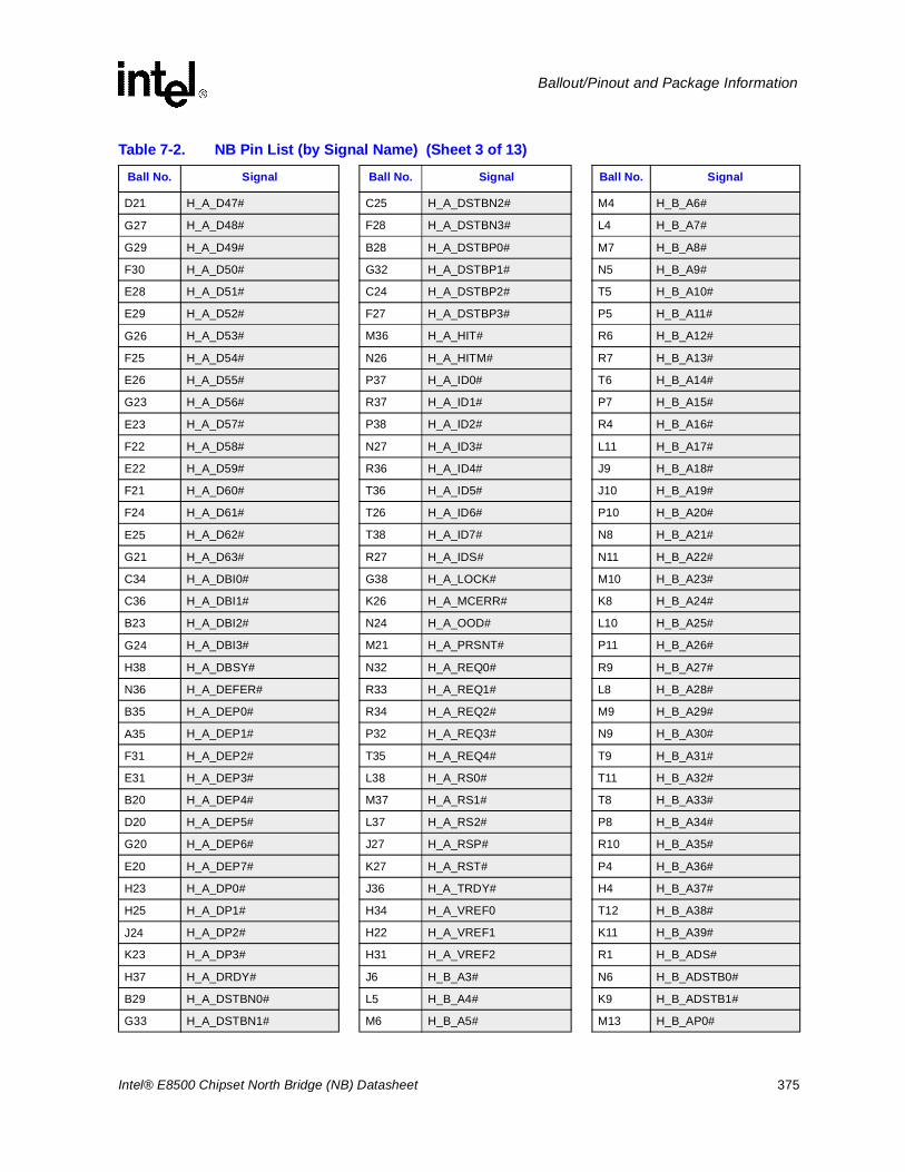
Intel® E8500 Chipset North Bridge (NB) Datasheet 375
Ballout/Pinout and Package Information
D21 H_A_D47# C25 H_A_DSTBN2# M4 H_B_A6#
G27 H_A_D48# F28 H_A_DSTBN3# L4 H_B_A7#
G29 H_A_D49# B28 H_A_DSTBP0# M7 H_B_A8#
F30 H_A_D50# G32 H_A_DSTBP1# N5 H_B_A9#
E28 H_A_D51# C24 H_A_DSTBP2# T5 H_B_A10#
E29 H_A_D52# F27 H_A_DSTBP3# P5 H_B_A11#
G26 H_A_D53# M36 H_A_HIT# R6 H_B_A12#
F25 H_A_D54# N26 H_A_HITM# R7 H_B_A13#
E26 H_A_D55# P37 H_A_ID0# T6 H_B_A14#
G23 H_A_D56# R37 H_A_ID1# P7 H_B_A15#
E23 H_A_D57# P38 H_A_ID2# R4 H_B_A16#
F22 H_A_D58# N27 H_A_ID3# L11 H_B_A17#
E22 H_A_D59# R36 H_A_ID4# J9 H_B_A18#
F21 H_A_D60# T36 H_A_ID5# J10 H_B_A19#
F24 H_A_D61# T26 H_A_ID6# P10 H_B_A20#
E25 H_A_D62# T38 H_A_ID7# N8 H_B_A21#
G21 H_A_D63# R27 H_A_IDS# N11 H_B_A22#
C34 H_A_DBI0# G38 H_A_LOCK# M10 H_B_A23#
C36 H_A_DBI1# K26 H_A_MCERR# K8 H_B_A24#
B23 H_A_DBI2# N24 H_A_OOD# L10 H_B_A25#
G24 H_A_DBI3# M21 H_A_PRSNT# P11 H_B_A26#
H38 H_A_DBSY# N32 H_A_REQ0# R9 H_B_A27#
N36 H_A_DEFER# R33 H_A_REQ1# L8 H_B_A28#
B35 H_A_DEP0# R34 H_A_REQ2# M9 H_B_A29#
A35 H_A_DEP1# P32 H_A_REQ3# N9 H_B_A30#
F31 H_A_DEP2# T35 H_A_REQ4# T9 H_B_A31#
E31 H_A_DEP3# L38 H_A_RS0# T11 H_B_A32#
B20 H_A_DEP4# M37 H_A_RS1# T8 H_B_A33#
D20 H_A_DEP5# L37 H_A_RS2# P8 H_B_A34#
G20 H_A_DEP6# J27 H_A_RSP# R10 H_B_A35#
E20 H_A_DEP7# K27 H_A_RST# P4 H_B_A36#
H23 H_A_DP0# J36 H_A_TRDY# H4 H_B_A37#
H25 H_A_DP1# H34 H_A_VREF0 T12 H_B_A38#
J24 H_A_DP2# H22 H_A_VREF1 K11 H_B_A39#
K23 H_A_DP3# H31 H_A_VREF2 R1 H_B_ADS#
H37 H_A_DRDY# J6 H_B_A3# N6 H_B_ADSTB0#
B29 H_A_DSTBN0# L5 H_B_A4# K9 H_B_ADSTB1#
G33 H_A_DSTBN1# M6 H_B_A5# M13 H_B_AP0#
Table 7-2. NB Pin List (by Signal Name) (Sheet 3 of 13)
Ball No. Signal Ball No. Signal Ball No. Signal
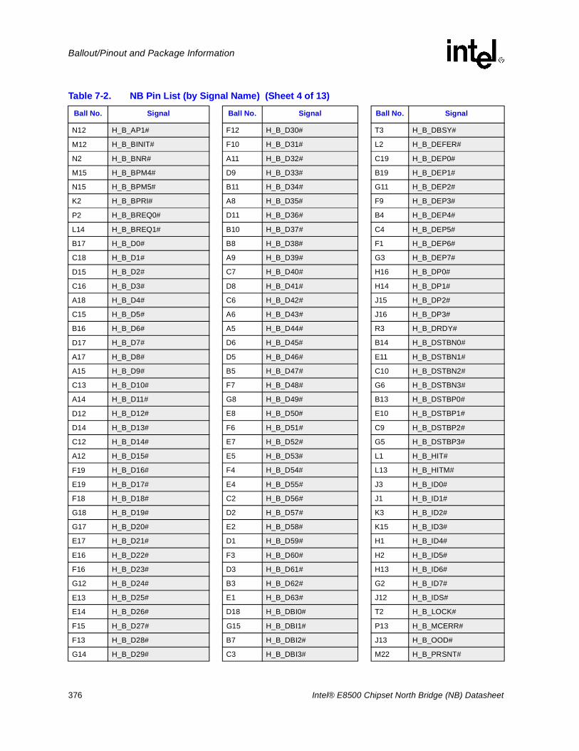
376 Intel® E8500 Chipset North Bridge (NB) Datasheet
Ballout/Pinout and Package Information
N12 H_B_AP1# F12 H_B_D30# T3 H_B_DBSY#
M12 H_B_BINIT# F10 H_B_D31# L2 H_B_DEFER#
N2 H_B_BNR# A11 H_B_D32# C19 H_B_DEP0#
M15 H_B_BPM4# D9 H_B_D33# B19 H_B_DEP1#
N15 H_B_BPM5# B11 H_B_D34# G11 H_B_DEP2#
K2 H_B_BPRI# A8 H_B_D35# F9 H_B_DEP3#
P2 H_B_BREQ0# D11 H_B_D36# B4 H_B_DEP4#
L14 H_B_BREQ1# B10 H_B_D37# C4 H_B_DEP5#
B17 H_B_D0# B8 H_B_D38# F1 H_B_DEP6#
C18 H_B_D1# A9 H_B_D39# G3 H_B_DEP7#
D15 H_B_D2# C7 H_B_D40# H16 H_B_DP0#
C16 H_B_D3# D8 H_B_D41# H14 H_B_DP1#
A18 H_B_D4# C6 H_B_D42# J15 H_B_DP2#
C15 H_B_D5# A6 H_B_D43# J16 H_B_DP3#
B16 H_B_D6# A5 H_B_D44# R3 H_B_DRDY#
D17 H_B_D7# D6 H_B_D45# B14 H_B_DSTBN0#
A17 H_B_D8# D5 H_B_D46# E11 H_B_DSTBN1#
A15 H_B_D9# B5 H_B_D47# C10 H_B_DSTBN2#
C13 H_B_D10# F7 H_B_D48# G6 H_B_DSTBN3#
A14 H_B_D11# G8 H_B_D49# B13 H_B_DSTBP0#
D12 H_B_D12# E8 H_B_D50# E10 H_B_DSTBP1#
D14 H_B_D13# F6 H_B_D51# C9 H_B_DSTBP2#
C12 H_B_D14# E7 H_B_D52# G5 H_B_DSTBP3#
A12 H_B_D15# E5 H_B_D53# L1 H_B_HIT#
F19 H_B_D16# F4 H_B_D54# L13 H_B_HITM#
E19 H_B_D17# E4 H_B_D55# J3 H_B_ID0#
F18 H_B_D18# C2 H_B_D56# J1 H_B_ID1#
G18 H_B_D19# D2 H_B_D57# K3 H_B_ID2#
G17 H_B_D20# E2 H_B_D58# K15 H_B_ID3#
E17 H_B_D21# D1 H_B_D59# H1 H_B_ID4#
E16 H_B_D22# F3 H_B_D60# H2 H_B_ID5#
F16 H_B_D23# D3 H_B_D61# H13 H_B_ID6#
G12 H_B_D24# B3 H_B_D62# G2 H_B_ID7#
E13 H_B_D25# E1 H_B_D63# J12 H_B_IDS#
E14 H_B_D26# D18 H_B_DBI0# T2 H_B_LOCK#
F15 H_B_D27# G15 H_B_DBI1# P13 H_B_MCERR#
F13 H_B_D28# B7 H_B_DBI2# J13 H_B_OOD#
G14 H_B_D29# C3 H_B_DBI3# M22 H_B_PRSNT#
Table 7-2. NB Pin List (by Signal Name) (Sheet 4 of 13)
Ball No. Signal Ball No. Signal Ball No. Signal
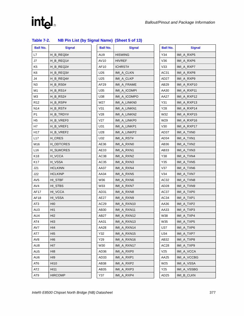
Intel® E8500 Chipset North Bridge (NB) Datasheet 377
Ballout/Pinout and Package Information
L7 H_B_REQ0# AU9 HISWING Y34 IMI_A_RXP5
J7 H_B_REQ1# AV10 HIVREF V36 IMI_A_RXP6
K5 H_B_REQ2# AF10 ICHRST# V33 IMI_A_RXP7
K6 H_B_REQ3# U26 IMI_A_CLKN AC31 IMI_A_RXP8
J4 H_B_REQ4# U25 IMI_A_CLKP AD27 IMI_A_RXP9
N3 H_B_RS0# AF29 IMI_A_FRAME AB29 IMI_A_RXP10
M1 H_B_RS1# U35 IMI_A_ICOMPI AA30 IMI_A_RXP11
M3 H_B_RS2# U38 IMI_A_ICOMPO AA27 IMI_A_RXP12
R12 H_B_RSP# W27 IMI_A_LINKN0 Y31 IMI_A_RXP13
N14 H_B_RST# V31 IMI_A_LINKN1 Y28 IMI_A_RXP14
P1 H_B_TRDY# V28 IMI_A_LINKN2 W32 IMI_A_RXP15
H5 H_B_VREF0 V27 IMI_A_LINKP0 W29 IMI_A_RXP16
H7 H_B_VREF1 U31 IMI_A_LINKP1 V30 IMI_A_RXP17
H17 H_B_VREF2 U28 IMI_A_LINKP2 AD37 IMI_A_TXN0
L17 H_CRES U32 IMI_A_RST# AD34 IMI_A_TXN1
M16 H_ODTCRES AE36 IMI_A_RXN0 AB36 IMI_A_TXN2
L16 H_SLWCRES AE33 IMI_A_RXN1 AB33 IMI_A_TXN3
K18 H_VCCA AC38 IMI_A_RXN2 Y38 IMI_A_TXN4
K17 H_VSSA AC35 IMI_A_RXN3 Y35 IMI_A_TXN5
J21 HCLKINN AA37 IMI_A_RXN4 V37 IMI_A_TXN6
J22 HCLKINP AA34 IMI_A_RXN5 V34 IMI_A_TXN7
AV5 HI_STBF W36 IMI_A_RXN6 AC32 IMI_A_TXN8
AV4 HI_STBS W33 IMI_A_RXN7 AD28 IMI_A_TXN9
AF17 HI_VCCA AD31 IMI_A_RXN8 AC37 IMI_A_TXP0
AF18 HI_VSSA AE27 IMI_A_RXN9 AC34 IMI_A_TXP1
AT3 HI0 AC29 IMI_A_RXN10 AA36 IMI_A_TXP2
AU3 HI1 AB30 IMI_A_RXN11 AA33 IMI_A_TXP3
AU4 HI2 AB27 IMI_A_RXN12 W38 IMI_A_TXP4
AT4 HI3 AA31 IMI_A_RXN13 W35 IMI_A_TXP5
AV7 HI4 AA28 IMI_A_RXN14 U37 IMI_A_TXP6
AT7 HI5 Y32 IMI_A_RXN15 U34 IMI_A_TXP7
AV8 HI6 Y29 IMI_A_RXN16 AB32 IMI_A_TXP8
AU8 HI7 W30 IMI_A_RXN17 AC28 IMI_A_TXP9
AU5 HI8 AD36 IMI_A_RXP0 V25 IMI_A_VCCA
AU6 HI9 AD33 IMI_A_RXP1 AA25 IMI_A_VCCBG
AT6 HI10 AB38 IMI_A_RXP2 W25 IMI_A_VSSA
AT2 HI11 AB35 IMI_A_RXP3 Y25 IMI_A_VSSBG
AT9 HIRCOMP Y37 IMI_A_RXP4 AD25 IMI_B_CLKN
Table 7-2. NB Pin List (by Signal Name) (Sheet 5 of 13)
Ball No. Signal Ball No. Signal Ball No. Signal
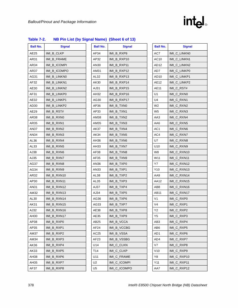
378 Intel® E8500 Chipset North Bridge (NB) Datasheet
Ballout/Pinout and Package Information
AE25 IMI_B_CLKP AF34 IMI_B_RXP9 AC7 IMI_C_LINKN0
AR31 IMI_B_FRAME AP32 IMI_B_RXP10 AC10 IMI_C_LINKN1
AR34 IMI_B_ICOMPI AN30 IMI_B_RXP11 AD12 IMI_C_LINKN2
AR37 IMI_B_ICOMPO AM31 IMI_B_RXP12 AD7 IMI_C_LINKP0
AG31 IMI_B_LINKN0 AL32 IMI_B_RXP13 AD10 IMI_C_LINKP1
AF32 IMI_B_LINKN1 AK30 IMI_B_RXP14 AE12 IMI_C_LINKP2
AE30 IMI_B_LINKN2 AJ31 IMI_B_RXP15 AE11 IMI_C_RST#
AF31 IMI_B_LINKP0 AH32 IMI_B_RXP16 U1 IMI_C_RXN0
AE32 IMI_B_LINKP1 AG30 IMI_B_RXP17 U4 IMI_C_RXN1
AD30 IMI_B_LINKP2 AP36 IMI_B_TXN0 W2 IMI_C_RXN2
AE29 IMI_B_RST# AP33 IMI_B_TXN1 W5 IMI_C_RXN3
AR38 IMI_B_RXN0 AM38 IMI_B_TXN2 AA3 IMI_C_RXN4
AR35 IMI_B_RXN1 AM35 IMI_B_TXN3 AA6 IMI_C_RXN5
AN37 IMI_B_RXN2 AK37 IMI_B_TXN4 AC1 IMI_C_RXN6
AN34 IMI_B_RXN3 AK34 IMI_B_TXN5 AC4 IMI_C_RXN7
AL36 IMI_B_RXN4 AH36 IMI_B_TXN6 U7 IMI_C_RXN8
AL33 IMI_B_RXN5 AH33 IMI_B_TXN7 U10 IMI_C_RXN9
AJ38 IMI_B_RXN6 AF38 IMI_B_TXN8 W8 IMI_C_RXN10
AJ35 IMI_B_RXN7 AF35 IMI_B_TXN9 W11 IMI_C_RXN11
AG37 IMI_B_RXN8 AN36 IMI_B_TXP0 Y7 IMI_C_RXN12
AG34 IMI_B_RXN9 AN33 IMI_B_TXP1 Y10 IMI_C_RXN13
AR32 IMI_B_RXN10 AL38 IMI_B_TXP2 AA9 IMI_C_RXN14
AP30 IMI_B_RXN11 AL35 IMI_B_TXP3 AA12 IMI_C_RXN15
AN31 IMI_B_RXN12 AJ37 IMI_B_TXP4 AB8 IMI_C_RXN16
AM32 IMI_B_RXN13 AJ34 IMI_B_TXP5 AB11 IMI_C_RXN17
AL30 IMI_B_RXN14 AG36 IMI_B_TXP6 V1 IMI_C_RXP0
AK31 IMI_B_RXN15 AG33 IMI_B_TXP7 V4 IMI_C_RXP1
AJ32 IMI_B_RXN16 AE38 IMI_B_TXP8 Y2 IMI_C_RXP2
AH30 IMI_B_RXN17 AE35 IMI_B_TXP9 Y5 IMI_C_RXP3
AP38 IMI_B_RXP0 AB25 IMI_B_VCCA AB3 IMI_C_RXP4
AP35 IMI_B_RXP1 AF24 IMI_B_VCCBG AB6 IMI_C_RXP5
AM37 IMI_B_RXP2 AC25 IMI_B_VSSA AD1 IMI_C_RXP6
AM34 IMI_B_RXP3 AF23 IMI_B_VSSBG AD4 IMI_C_RXP7
AK36 IMI_B_RXP4 U14 IMI_C_CLKN V7 IMI_C_RXP8
AK33 IMI_B_RXP5 T14 IMI_C_CLKP V10 IMI_C_RXP9
AH38 IMI_B_RXP6 U11 IMI_C_FRAME Y8 IMI_C_RXP10
AH35 IMI_B_RXP7 U2 IMI_C_ICOMPI Y11 IMI_C_RXP11
AF37 IMI_B_RXP8 U5 IMI_C_ICOMPO AA7 IMI_C_RXP12
Table 7-2. NB Pin List (by Signal Name) (Sheet 6 of 13)
Ball No. Signal Ball No. Signal Ball No. Signal
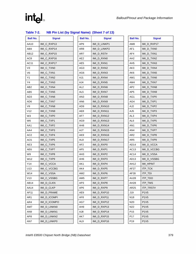
Intel® E8500 Chipset North Bridge (NB) Datasheet 379
Ballout/Pinout and Package Information
AA10 IMI_C_RXP13 AP9 IMI_D_LINKP1 AM8 IMI_D_RXP17
AB9 IMI_C_RXP14 AR8 IMI_D_LINKP2 AF1 IMI_D_TXN0
AB12 IMI_C_RXP15 AR7 IMI_D_RST# AF4 IMI_D_TXN1
AC8 IMI_C_RXP16 AE2 IMI_D_RXN0 AH2 IMI_D_TXN2
AC11 IMI_C_RXP17 AE5 IMI_D_RXN1 AH5 IMI_D_TXN3
V3 IMI_C_TXN0 AG3 IMI_D_RXN2 AK3 IMI_D_TXN4
V6 IMI_C_TXN1 AG6 IMI_D_RXN3 AK6 IMI_D_TXN5
Y1 IMI_C_TXN2 AJ1 IMI_D_RXN4 AM1 IMI_D_TXN6
Y4 IMI_C_TXN3 AJ4 IMI_D_RXN5 AM4 IMI_D_TXN7
AB2 IMI_C_TXN4 AL2 IMI_D_RXN6 AP2 IMI_D_TXN8
AB5 IMI_C_TXN5 AL5 IMI_D_RXN7 AP5 IMI_D_TXN9
AD3 IMI_C_TXN6 AN3 IMI_D_RXN8 AG1 IMI_D_TXP0
AD6 IMI_C_TXN7 AN6 IMI_D_RXN9 AG4 IMI_D_TXP1
V9 IMI_C_TXN8 AD9 IMI_D_RXN10 AJ2 IMI_D_TXP2
V12 IMI_C_TXN9 AE8 IMI_D_RXN11 AJ5 IMI_D_TXP3
W3 IMI_C_TXP0 AF7 IMI_D_RXN12 AL3 IMI_D_TXP4
W6 IMI_C_TXP1 AG9 IMI_D_RXN13 AL6 IMI_D_TXP5
AA1 IMI_C_TXP2 AH8 IMI_D_RXN14 AN1 IMI_D_TXP6
AA4 IMI_C_TXP3 AJ7 IMI_D_RXN15 AN4 IMI_D_TXP7
AC2 IMI_C_TXP4 AK9 IMI_D_RXN16 AR2 IMI_D_TXP8
AC5 IMI_C_TXP5 AL8 IMI_D_RXN17 AR5 IMI_D_TXP9
AE3 IMI_C_TXP6 AF2 IMI_D_RXP0 AD14 IMI_D_VCCA
AE6 IMI_C_TXP7 AF5 IMI_D_RXP1 AC13 IMI_D_VCCBG
W9 IMI_C_TXP8 AH3 IMI_D_RXP2 AC14 IMI_D_VSSA
W12 IMI_C_TXP9 AH6 IMI_D_RXP3 AD13 IMI_D_VSSBG
Y14 IMI_C_VCCA AK1 IMI_D_RXP4 AH12 IMI_HPINT
U13 IMI_C_VCCBG AK4 IMI_D_RXP5 AF27 ITP_TCK
W14 IMI_C_VSSA AM2 IMI_D_RXP6 AF28 ITP_TDI
V13 IMI_C_VSSBG AM5 IMI_D_RXP7 AU28 ITP_TDO
AB14 IMI_D_CLKN AP3 IMI_D_RXP8 AH28 ITP_TMS
AA14 IMI_D_CLKP AP6 IMI_D_RXP9 AR25 ITP_TRST#
AF11 IMI_D_FRAME AE9 IMI_D_RXP10 J19 P1V5
AR1 IMI_D_ICOMPI AF8 IMI_D_RXP11 N18 P1V5
AR4 IMI_D_ICOMPO AG7 IMI_D_RXP12 N20 P1V5
AM7 IMI_D_LINKN0 AH9 IMI_D_RXP13 N22 P1V5
AN9 IMI_D_LINKN1 AJ8 IMI_D_RXP14 P15 P1V5
AP8 IMI_D_LINKN2 AK7 IMI_D_RXP15 P17 P1V5
AN7 IMI_D_LINKP0 AL9 IMI_D_RXP16 P19 P1V5
Table 7-2. NB Pin List (by Signal Name) (Sheet 7 of 13)
Ball No. Signal Ball No. Signal Ball No. Signal
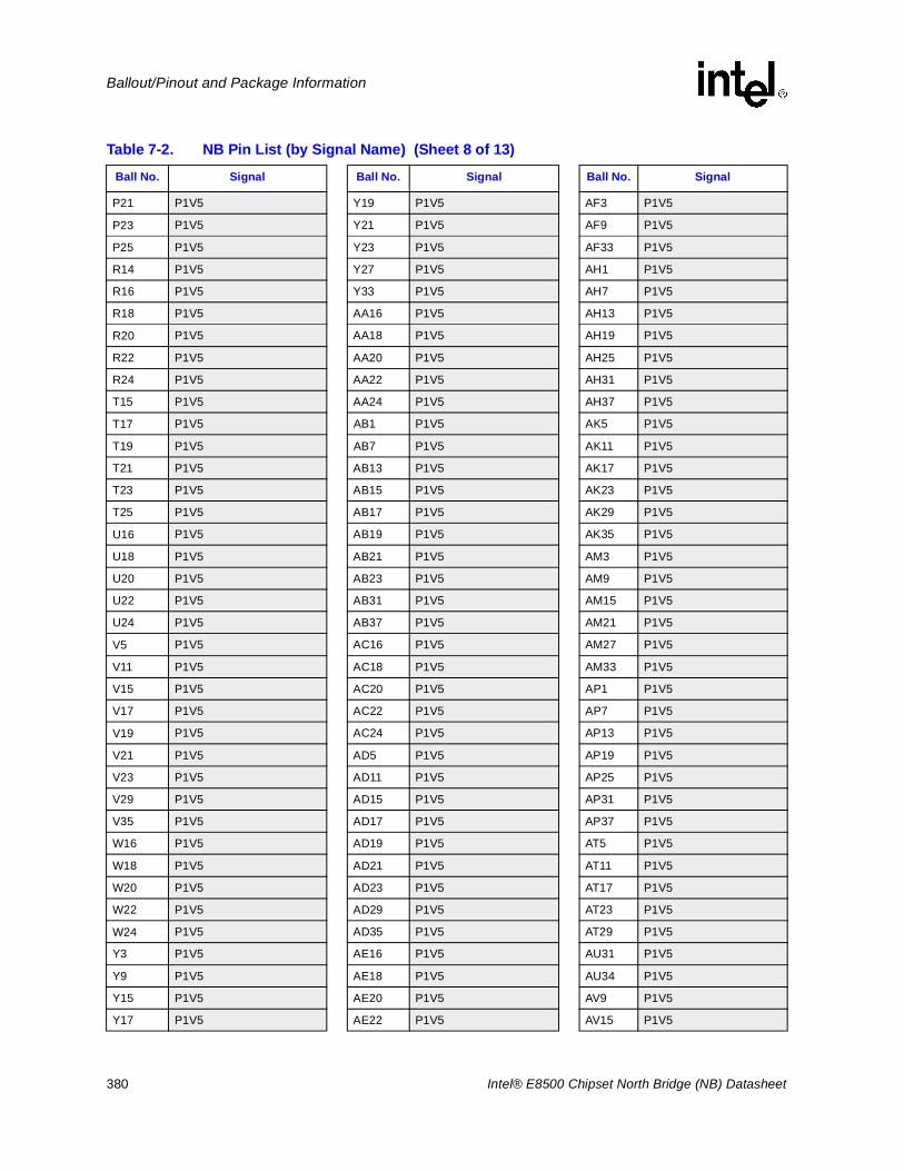
380 Intel® E8500 Chipset North Bridge (NB) Datasheet
Ballout/Pinout and Package Information
P21 P1V5 Y19 P1V5 AF3 P1V5
P23 P1V5 Y21 P1V5 AF9 P1V5
P25 P1V5 Y23 P1V5 AF33 P1V5
R14 P1V5 Y27 P1V5 AH1 P1V5
R16 P1V5 Y33 P1V5 AH7 P1V5
R18 P1V5 AA16 P1V5 AH13 P1V5
R20 P1V5 AA18 P1V5 AH19 P1V5
R22 P1V5 AA20 P1V5 AH25 P1V5
R24 P1V5 AA22 P1V5 AH31 P1V5
T15 P1V5 AA24 P1V5 AH37 P1V5
T17 P1V5 AB1 P1V5 AK5 P1V5
T19 P1V5 AB7 P1V5 AK11 P1V5
T21 P1V5 AB13 P1V5 AK17 P1V5
T23 P1V5 AB15 P1V5 AK23 P1V5
T25 P1V5 AB17 P1V5 AK29 P1V5
U16 P1V5 AB19 P1V5 AK35 P1V5
U18 P1V5 AB21 P1V5 AM3 P1V5
U20 P1V5 AB23 P1V5 AM9 P1V5
U22 P1V5 AB31 P1V5 AM15 P1V5
U24 P1V5 AB37 P1V5 AM21 P1V5
V5 P1V5 AC16 P1V5 AM27 P1V5
V11 P1V5 AC18 P1V5 AM33 P1V5
V15 P1V5 AC20 P1V5 AP1 P1V5
V17 P1V5 AC22 P1V5 AP7 P1V5
V19 P1V5 AC24 P1V5 AP13 P1V5
V21 P1V5 AD5 P1V5 AP19 P1V5
V23 P1V5 AD11 P1V5 AP25 P1V5
V29 P1V5 AD15 P1V5 AP31 P1V5
V35 P1V5 AD17 P1V5 AP37 P1V5
W16 P1V5 AD19 P1V5 AT5 P1V5
W18 P1V5 AD21 P1V5 AT11 P1V5
W20 P1V5 AD23 P1V5 AT17 P1V5
W22 P1V5 AD29 P1V5 AT23 P1V5
W24 P1V5 AD35 P1V5 AT29 P1V5
Y3 P1V5 AE16 P1V5 AU31 P1V5
Y9 P1V5 AE18 P1V5 AU34 P1V5
Y15 P1V5 AE20 P1V5 AV9 P1V5
Y17 P1V5 AE22 P1V5 AV15 P1V5
Table 7-2. NB Pin List (by Signal Name) (Sheet 8 of 13)
Ball No. Signal Ball No. Signal Ball No. Signal
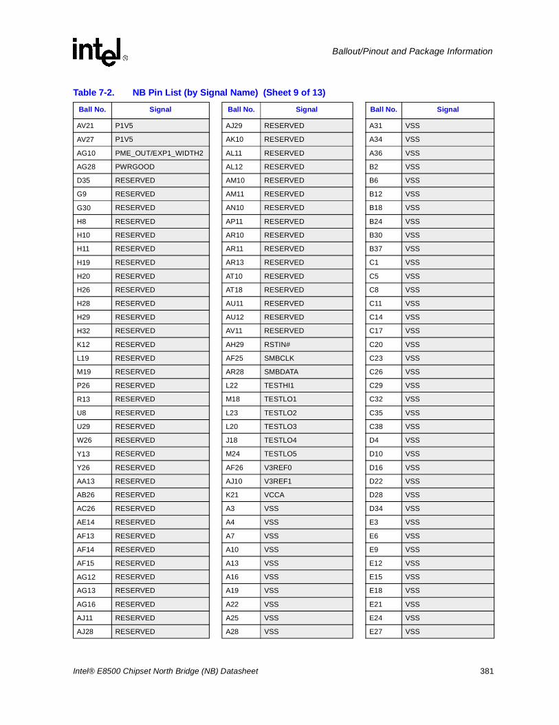
Intel® E8500 Chipset North Bridge (NB) Datasheet 381
Ballout/Pinout and Package Information
AV21 P1V5 AJ29 RESERVED A31 VSS
AV27 P1V5 AK10 RESERVED A34 VSS
AG10 PME_OUT/EXP1_WIDTH2 AL11 RESERVED A36 VSS
AG28 PWRGOOD AL12 RESERVED B2 VSS
D35 RESERVED AM10 RESERVED B6 VSS
G9 RESERVED AM11 RESERVED B12 VSS
G30 RESERVED AN10 RESERVED B18 VSS
H8 RESERVED AP11 RESERVED B24 VSS
H10 RESERVED AR10 RESERVED B30 VSS
H11 RESERVED AR11 RESERVED B37 VSS
H19 RESERVED AR13 RESERVED C1 VSS
H20 RESERVED AT10 RESERVED C5 VSS
H26 RESERVED AT18 RESERVED C8 VSS
H28 RESERVED AU11 RESERVED C11 VSS
H29 RESERVED AU12 RESERVED C14 VSS
H32 RESERVED AV11 RESERVED C17 VSS
K12 RESERVED AH29 RSTIN# C20 VSS
L19 RESERVED AF25 SMBCLK C23 VSS
M19 RESERVED AR28 SMBDATA C26 VSS
P26 RESERVED L22 TESTHI1 C29 VSS
R13 RESERVED M18 TESTLO1 C32 VSS
U8 RESERVED L23 TESTLO2 C35 VSS
U29 RESERVED L20 TESTLO3 C38 VSS
W26 RESERVED J18 TESTLO4 D4 VSS
Y13 RESERVED M24 TESTLO5 D10 VSS
Y26 RESERVED AF26 V3REF0 D16 VSS
AA13 RESERVED AJ10 V3REF1 D22 VSS
AB26 RESERVED K21 VCCA D28 VSS
AC26 RESERVED A3 VSS D34 VSS
AE14 RESERVED A4 VSS E3 VSS
AF13 RESERVED A7 VSS E6 VSS
AF14 RESERVED A10 VSS E9 VSS
AF15 RESERVED A13 VSS E12 VSS
AG12 RESERVED A16 VSS E15 VSS
AG13 RESERVED A19 VSS E18 VSS
AG16 RESERVED A22 VSS E21 VSS
AJ11 RESERVED A25 VSS E24 VSS
AJ28 RESERVED A28 VSS E27 VSS
Table 7-2. NB Pin List (by Signal Name) (Sheet 9 of 13)
Ball No. Signal Ball No. Signal Ball No. Signal
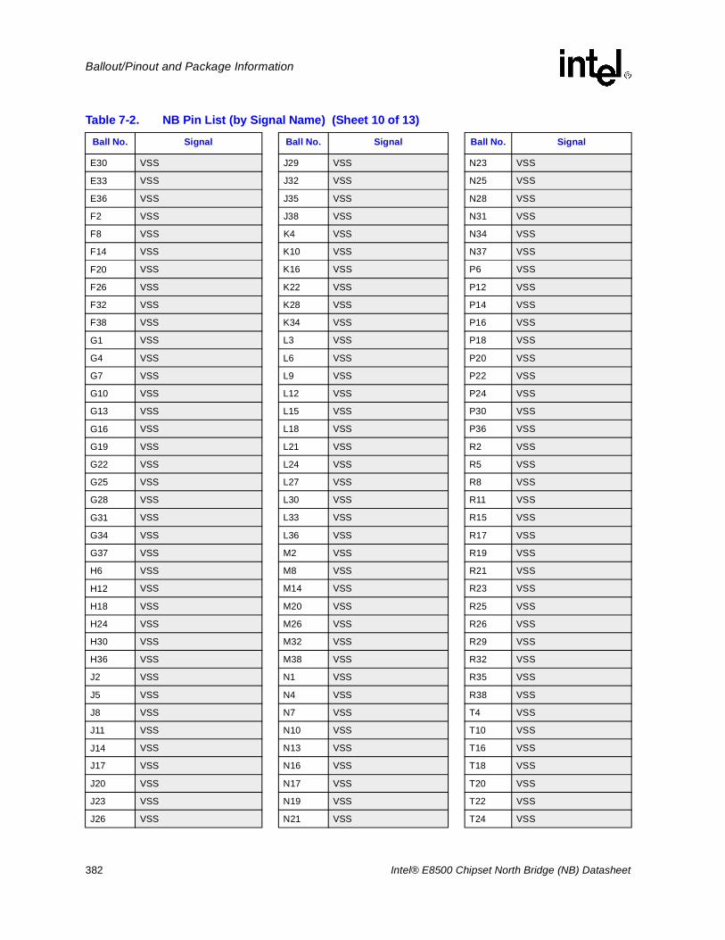
382 Intel® E8500 Chipset North Bridge (NB) Datasheet
Ballout/Pinout and Package Information
E30 VSS J29 VSS N23 VSS
E33 VSS J32 VSS N25 VSS
E36 VSS J35 VSS N28 VSS
F2 VSS J38 VSS N31 VSS
F8 VSS K4 VSS N34 VSS
F14 VSS K10 VSS N37 VSS
F20 VSS K16 VSS P6 VSS
F26 VSS K22 VSS P12 VSS
F32 VSS K28 VSS P14 VSS
F38 VSS K34 VSS P16 VSS
G1 VSS L3 VSS P18 VSS
G4 VSS L6 VSS P20 VSS
G7 VSS L9 VSS P22 VSS
G10 VSS L12 VSS P24 VSS
G13 VSS L15 VSS P30 VSS
G16 VSS L18 VSS P36 VSS
G19 VSS L21 VSS R2 VSS
G22 VSS L24 VSS R5 VSS
G25 VSS L27 VSS R8 VSS
G28 VSS L30 VSS R11 VSS
G31 VSS L33 VSS R15 VSS
G34 VSS L36 VSS R17 VSS
G37 VSS M2 VSS R19 VSS
H6 VSS M8 VSS R21 VSS
H12 VSS M14 VSS R23 VSS
H18 VSS M20 VSS R25 VSS
H24 VSS M26 VSS R26 VSS
H30 VSS M32 VSS R29 VSS
H36 VSS M38 VSS R32 VSS
J2 VSS N1 VSS R35 VSS
J5 VSS N4 VSS R38 VSS
J8 VSS N7 VSS T4 VSS
J11 VSS N10 VSS T10 VSS
J14 VSS N13 VSS T16 VSS
J17 VSS N16 VSS T18 VSS
J20 VSS N17 VSS T20 VSS
J23 VSS N19 VSS T22 VSS
J26 VSS N21 VSS T24 VSS
Table 7-2. NB Pin List (by Signal Name) (Sheet 10 of 13)
Ball No. Signal Ball No. Signal Ball No. Signal
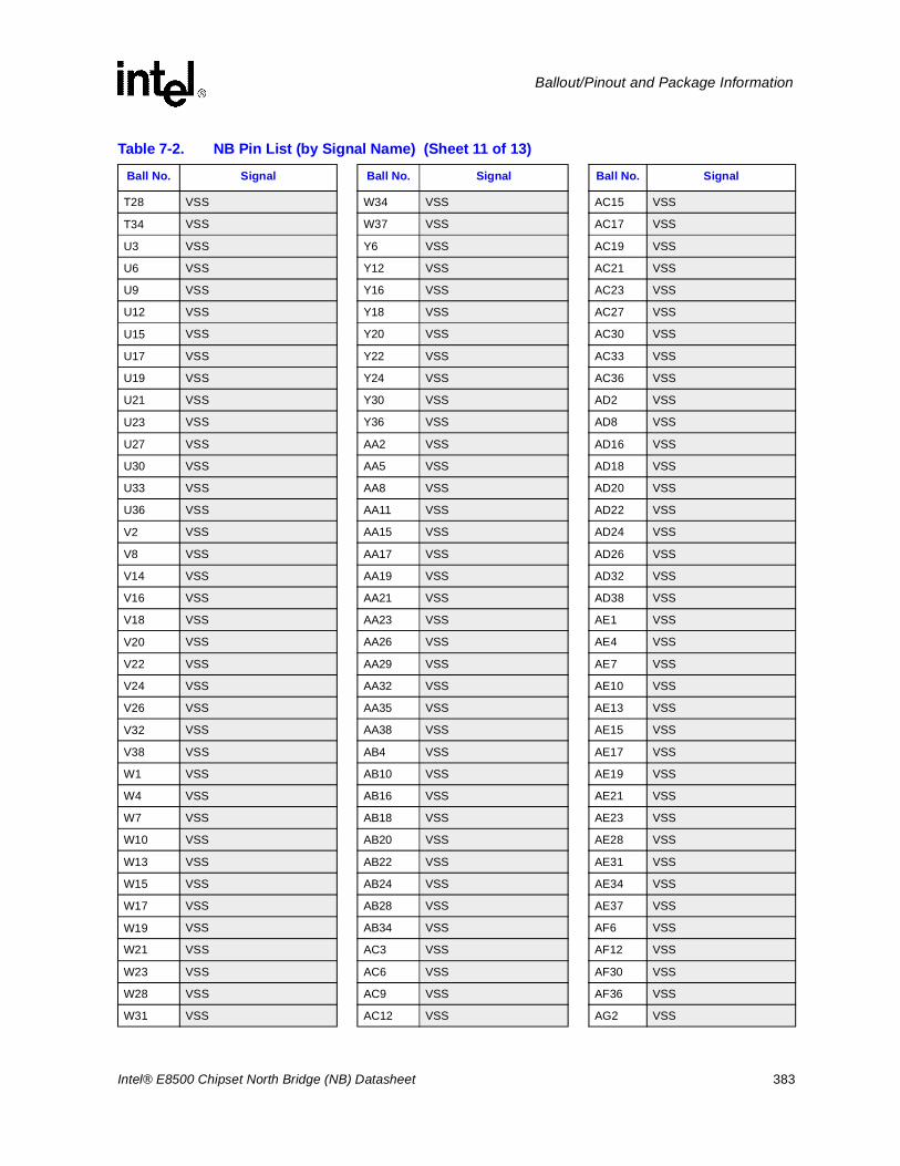
Intel® E8500 Chipset North Bridge (NB) Datasheet 383
Ballout/Pinout and Package Information
T28 VSS W34 VSS AC15 VSS
T34 VSS W37 VSS AC17 VSS
U3 VSS Y6 VSS AC19 VSS
U6 VSS Y12 VSS AC21 VSS
U9 VSS Y16 VSS AC23 VSS
U12 VSS Y18 VSS AC27 VSS
U15 VSS Y20 VSS AC30 VSS
U17 VSS Y22 VSS AC33 VSS
U19 VSS Y24 VSS AC36 VSS
U21 VSS Y30 VSS AD2 VSS
U23 VSS Y36 VSS AD8 VSS
U27 VSS AA2 VSS AD16 VSS
U30 VSS AA5 VSS AD18 VSS
U33 VSS AA8 VSS AD20 VSS
U36 VSS AA11 VSS AD22 VSS
V2 VSS AA15 VSS AD24 VSS
V8 VSS AA17 VSS AD26 VSS
V14 VSS AA19 VSS AD32 VSS
V16 VSS AA21 VSS AD38 VSS
V18 VSS AA23 VSS AE1 VSS
V20 VSS AA26 VSS AE4 VSS
V22 VSS AA29 VSS AE7 VSS
V24 VSS AA32 VSS AE10 VSS
V26 VSS AA35 VSS AE13 VSS
V32 VSS AA38 VSS AE15 VSS
V38 VSS AB4 VSS AE17 VSS
W1 VSS AB10 VSS AE19 VSS
W4 VSS AB16 VSS AE21 VSS
W7 VSS AB18 VSS AE23 VSS
W10 VSS AB20 VSS AE28 VSS
W13 VSS AB22 VSS AE31 VSS
W15 VSS AB24 VSS AE34 VSS
W17 VSS AB28 VSS AE37 VSS
W19 VSS AB34 VSS AF6 VSS
W21 VSS AC3 VSS AF12 VSS
W23 VSS AC6 VSS AF30 VSS
W28 VSS AC9 VSS AF36 VSS
W31 VSS AC12 VSS AG2 VSS
Table 7-2. NB Pin List (by Signal Name) (Sheet 11 of 13)
Ball No. Signal Ball No. Signal Ball No. Signal
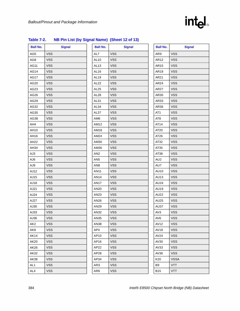
384 Intel® E8500 Chipset North Bridge (NB) Datasheet
Ballout/Pinout and Package Information
AG5 VSS AL7 VSS AR9 VSS
AG8 VSS AL10 VSS AR12 VSS
AG11 VSS AL13 VSS AR15 VSS
AG14 VSS AL16 VSS AR18 VSS
AG17 VSS AL19 VSS AR21 VSS
AG20 VSS AL22 VSS AR24 VSS
AG23 VSS AL25 VSS AR27 VSS
AG26 VSS AL28 VSS AR30 VSS
AG29 VSS AL31 VSS AR33 VSS
AG32 VSS AL34 VSS AR36 VSS
AG35 VSS AL37 VSS AT1 VSS
AG38 VSS AM6 VSS AT8 VSS
AH4 VSS AM12 VSS AT14 VSS
AH10 VSS AM18 VSS AT20 VSS
AH16 VSS AM24 VSS AT26 VSS
AH22 VSS AM30 VSS AT32 VSS
AH34 VSS AM36 VSS AT35 VSS
AJ3 VSS AN2 VSS AT38 VSS
AJ6 VSS AN5 VSS AU2 VSS
AJ9 VSS AN8 VSS AU7 VSS
AJ12 VSS AN11 VSS AU10 VSS
AJ15 VSS AN14 VSS AU13 VSS
AJ18 VSS AN17 VSS AU16 VSS
AJ21 VSS AN20 VSS AU19 VSS
AJ24 VSS AN23 VSS AU22 VSS
AJ27 VSS AN26 VSS AU25 VSS
AJ30 VSS AN29 VSS AU37 VSS
AJ33 VSS AN32 VSS AV3 VSS
AJ36 VSS AN35 VSS AV6 VSS
AK2 VSS AN38 VSS AV12 VSS
AK8 VSS AP4 VSS AV18 VSS
AK14 VSS AP10 VSS AV24 VSS
AK20 VSS AP16 VSS AV30 VSS
AK26 VSS AP22 VSS AV33 VSS
AK32 VSS AP28 VSS AV36 VSS
AK38 VSS AP34 VSS K20 VSSA
AL1 VSS AR3 VSS B9 VTT
AL4 VSS AR6 VSS B15 VTT
Table 7-2. NB Pin List (by Signal Name) (Sheet 12 of 13)
Ball No. Signal Ball No. Signal Ball No. Signal
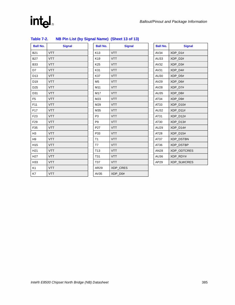
Intel® E8500 Chipset North Bridge (NB) Datasheet 385
Ballout/Pinout and Package Information
B21 VTT K13 VTT AV34 XDP_D1#
B27 VTT K19 VTT AU33 XDP_D2#
B33 VTT K25 VTT AV32 XDP_D3#
D7 VTT K31 VTT AV31 XDP_D4#
D13 VTT K37 VTT AU30 XDP_D5#
D19 VTT M5 VTT AV29 XDP_D6#
D25 VTT M11 VTT AV28 XDP_D7#
D31 VTT M17 VTT AU35 XDP_D8#
F5 VTT M23 VTT AT34 XDP_D9#
F11 VTT M29 VTT AT33 XDP_D10#
F17 VTT M35 VTT AU32 XDP_D11#
F23 VTT P3 VTT AT31 XDP_D12#
F29 VTT P9 VTT AT30 XDP_D13#
F35 VTT P27 VTT AU29 XDP_D14#
H3 VTT P33 VTT AT28 XDP_D15#
H9 VTT T1 VTT AT37 XDP_DSTBN
H15 VTT T7 VTT AT36 XDP_DSTBP
H21 VTT T13 VTT AN28 XDP_ODTCRES
H27 VTT T31 VTT AU36 XDP_RDY#
H33 VTT T37 VTT AP29 XDP_SLWCRES
K1 VTT AR29 XDP_CRES
K7 VTT AV35 XDP_D0#
Table 7-2. NB Pin List (by Signal Name) (Sheet 13 of 13)
Ball No. Signal Ball No. Signal Ball No. Signal
386 Intel® E8500 Chipset North Bridge (NB) Datasheet
Ballout/Pinout and Package Information
7.2 Intel® E8501 Chipset North Bridge (NB) Mechanical Package InformationFor the NB Mechanical Package drawing, refer to Figure 7-5 through Figure 7-7.
For detailed information about the XMB Mechanical specification, refer to the Intel® E8501 Chipset eXternal Memory Bridge (XMB) Datasheet.
For detailed information about the ICH5 mechanical specifications, refer to the Intel® 82801EBI/O Controller Hub 5 (ICH5) and Intel® 82801ER I/O Controller Hub 5 (ICH5R) Datasheet. The ICH5 Datasheet is available at: http://developer.intel.com/design/chipsets/datashts.
For detailed information about the Intel 6700PXH/6702PXH 64-bit PCI Hub ballout and pin list, refer to the Intel® 6700PXH 64-bit PCI Hub and Intel® 6702PXH 64-bit PCI Hub Datasheet.
Figure 7-5. Intel® E8501 Chipset North Bridge (NB) Package Dimensions (Top View)
NBIHS
42.5 mm.
42.5 mm.38.5 mm.
38.5 mm
Handling
Exclusion
Area
Intel® E8500 Chipset North Bridge (NB) Datasheet 387
Ballout/Pinout and Package Information
Figure 7-6. NB Package Dimensions (Side View)
0.20 –C–
IHS Substrate
0.435 ± 0.025 mmSee note 3
Seating Plane
2.44 ± 0.071 mm
See note 1.
Notes:1. Primary datum -C- and seating plan are defined by the spherical crowns of the solder balls (shown before motherboard attach)2. All dimensions and tolerances conform to ANSI Y14.5M-19943. BGA has a pre-SMT height of 0.5mm and post-SMT height of 0.41-0.46mm4. Shown before motherboard attach; FCBGA has a convex (dome shaped) orientation before reflow and is expected to have a slightly concave(bowl shaped) orientation after reflow
0.20 See note 4.
3.79 ± 0.144 mm
4.23 ± 0.146 mm
388 Intel® E8500 Chipset North Bridge (NB) Datasheet
Ballout/Pinout and Package Information
§
Figure 7-7. NB Package Dimensions (Bottom View)
42.5 + 0.05
11 2523211917151397531 27 29 3733 35312822 26242018161412108642 36343230 38
A
AJ
AE
AC
AA
U
R
N
L
J
G
E
C
W
AG
AL
AN
AR
AU
AH
AF
AD
AB
Y
V
T
P
M
K
H
F
D
AK
AM
AP
AT
AV
B
A
B42.5 + 0.05C A0.2
37X 1.092
20.202
20.202
37X 1.092