
Intel 82802AB/82802AC Firmware Hub (FWH) - · PDF fileIntel® 82802AB/82802AC Firmware Hub...
53
Intel ® 82802AB/82802AC Firmware Hub (FWH) Datasheet May 2000 Document Number: 290658-003 R
Transcript of Intel 82802AB/82802AC Firmware Hub (FWH) - · PDF fileIntel® 82802AB/82802AC Firmware Hub...

Intel® 82802AB/82802ACFirmware Hub (FWH)Datasheet
May 2000
Document Number: 290658-003
R

Intel® 82802AB/AC Firmware Hub
R
2 Datasheet
Information in this document is provided in connection with Intel products. No license, express or implied, by estoppel or otherwise, to any intellectualproperty rights is granted by this document. Except as provided in Intel’s Terms and Conditions of Sale for such products, Intel assumes no liabilitywhatsoever, and Intel disclaims any express or implied warranty, relating to sale and/or use of Intel products including liability or warranties relating tofitness for a particular purpose, merchantability, or infringement of any patent, copyright or other intellectual property right. Intel products are notintended for use in medical, life saving, or life sustaining applications.
Intel may make changes to specifications and product descriptions at any time, without notice.
Designers must not rely on the absence or characteristics of any features or instructions marked "reserved" or "undefined." Intel reserves these forfuture definition and shall have no responsibility whatsoever for conflicts or incompatibilities arising from future changes to them.
The Intel® 82802AB/AC (FWH) may contain design defects or errors known as errata which may cause the product to deviate from publishedspecifications. Current characterized errata are available on request.
Contact your local Intel sales office or your distributor to obtain the latest specifications and before placing your product order.
I2C is a 2-wire communications bus/protocol developed by Philips. SMBus is a subset of the I2C bus/protocol and was developed by Intel.Implementations of the I2C bus/protocol may require licenses from various entities, including Philips Electronics N.V. and North American PhilipsCorporation.
Alert on LAN is a result of the Intel-IBM Advanced Manageability Alliance and a trademark of IBM
Copies of documents which have an ordering number and are referenced in this document, or other Intel literature, may be obtained from:
Intel Corporation
www.intel.com
or call 1-800-548-4725
*Third-party brands and names are the property of their respective owners.
Copyright © Intel Corporation 1999, 2000

Intel® 82802AB/AC Firmware Hub
R
Datasheet 3
Contents
1. Architectural Overview ..........................................................................................................9
1.1. Interface Overview.....................................................................................................91.1.1. Firmware Hub Interface .......................................................................... 101.1.2. Address/Address-Multiplexed Interface.................................................... 10
1.2. Nonvolatile Flash Memory Core ............................................................................... 10
2. Pinout Configurations ......................................................................................................... 13
2.1. Pin Descriptions..................................................................................................... 14
3. Interface Operation Description ........................................................................................... 17
3.1. Read..................................................................................................................... 173.2. Write..................................................................................................................... 173.3. Output Disable....................................................................................................... 173.4. Reset .................................................................................................................... 173.5. Operational Effects of Hardware Write-Protect Pins TBL# and WP#............................ 18
4. Functional Descriptions ...................................................................................................... 19
4.1. Read Array Command ............................................................................................ 214.2. Read Identifier Codes Command.............................................................................. 214.3. Read Status Register Command.............................................................................. 214.4. Clear Status Register Command.............................................................................. 214.5. Block Erase Command........................................................................................... 224.6. Program Command ................................................................................................ 224.7. Block Erase Suspend Command ............................................................................. 234.8. Program Suspend Comand ..................................................................................... 234.9. Register Based Locking, General-Purpose Input, and Random Number Generator
Registers .............................................................................................................. 234.9.1. T_BLOCK_LK and T_MINUSxx_LK — Block-Locking Registers................. 254.9.2. General-Purpose Input Register .............................................................. 27
4.9.2.1. GPI_REG — General-Purpose Input Register ............................... 274.9.3. Random Number Generator Registers ..................................................... 28
4.9.3.1. RNG Hardware Status Register................................................... 284.9.3.2. RNG Data Status Register.......................................................... 284.9.3.3. RNG Data Register .................................................................... 29
4.10. Using the Random Number Generator ...................................................................... 294.11. Detecting and Initializing the RNG Device................................................................. 29
4.11.1. Detecting the RNG Device...................................................................... 294.11.2. Initializing the RNG Device ..................................................................... 304.11.3. Selecting Appropriate FWH IDs and Densities.......................................... 304.11.4. Mapping FWH Devices onto Memory Map ............................................... 314.11.5. Paging FWH Devices for Greater Than 4 MB of FWH Memory ................... 314.11.6. Programming Multiple FWH Devices ....................................................... 31
4.12. CUI Automation Flowcharts..................................................................................... 32
5. Electrical Specifications ..................................................................................................... 34

Intel® 82802AB/AC Firmware Hub
R
4 Datasheet
5.1. Absolute Maximum Ratings .................................................................................... 345.2. Operating Conditions .............................................................................................. 34
5.2.1. Interface DC Input/Output Specifications .................................................. 355.2.2. Interface AC Input/Output Specifications .................................................. 375.2.3. FWH Interface AC Timing Specifications.................................................. 38
5.2.3.1. Clock Specification .................................................................... 385.2.3.2. Signal Timing Parameters........................................................... 39
5.3. Block Programming Times ...................................................................................... 415.4. Firmware Hub Interface........................................................................................... 41
5.4.1. FWH Interface Cycles ............................................................................ 415.4.1.1. Read Cycle Sequence................................................................ 415.4.1.2. Single-Byte Read Waveforms...................................................... 435.4.1.3. Write Cycle Sequence ............................................................... 435.4.1.4. Write Waveforms ....................................................................... 445.4.1.5. Response To Invalid Fields ......................................................... 445.4.1.6. Abort Operations ....................................................................... 455.4.1.7. FWH Cycle Timing Information.................................................... 45
5.5. RNG Parameters.................................................................................................... 46
6. PROM Programming Specifications..................................................................................... 48
6.1. Programming (“A/A Mux”) Mode Operation ............................................................... 486.2. Bus Operation........................................................................................................ 48
6.2.1. Output Disable/Enable ........................................................................... 486.2.2. Row/Column Addresses ......................................................................... 486.2.3. Read Operation ..................................................................................... 486.2.4. Read Identifier Codes Operation.............................................................. 496.2.5. Write Operation..................................................................................... 49
6.3. Command Definitions.............................................................................................. 496.4. Electrical Characteristics in A/A Mux Mode.............................................................. 49
6.4.1. Reset Operations .................................................................................. 506.4.2. AC Waveforms for Reset Operations ....................................................... 506.4.3. A/A Mux Read-Only Operations (1,3) ......................................................... 506.4.4. A/A Mux Write Operations (1,2) ................................................................ 52
Intel® 82802AB/AC Firmware Hub
R
Datasheet 5
Figures
Figure 1. Simplified Block Diagram ...................................................................................8Figure 2. Device Memory Map with FWH Hardware Lock Architecture................................ 11Figure 3. FWH Boot-Configuration System Memory Map .................................................. 11Figure 4. 32-Lead PLCC Firmware Hub Pinout ................................................................. 13Figure 5. 40-Lead TSOP Firmware Hub Pinout ................................................................. 13Figure 6. Automated Block Erase Flowchart .................................................................... 32Figure 7. Clock Waveform .............................................................................................. 38Figure 8. Output Timing Parameters................................................................................ 39Figure 9. Input Timing Parameters .................................................................................. 40Figure 10. FWH Single-Byte Read Waveforms................................................................... 43Figure 11. Write Waveforms............................................................................................. 44Figure 12. FWH Output Timing Parameters ....................................................................... 46Figure 13. FWH Input Timing Parameters .......................................................................... 47Figure 14. A/A Mux Read Timing Diagram......................................................................... 51Figure 15. A/A Mux Write Timing Diagram......................................................................... 53
Tables
Table 1. Pin Descriptions .............................................................................................. 14Table 2. Command Definitions ....................................................................................... 19Table 3. Status Register Definition................................................................................. 20Table 4. Identifier Codes ............................................................................................... 21Table 5. Firmware Hub Register Configuration Map.......................................................... 24Table 6. Register-Based Locking Value Definitions .......................................................... 25Table 7. Temperature and VCC...................................................................................... 34Table 8. FWH Interface DC Input/Output Specifications ................................................... 35Table 9. Power Supply Specifications — All Interfaces .................................................... 36Table 10. FWH Interface AC Input/Output Specifications ................................................... 37Table 11. Clock Specification.......................................................................................... 38Table 12. Signal Timing Parameters ................................................................................ 39Table 13. Interface Measurement Condition Parameters .................................................... 40Table 14. AC Waveform for Reset Operation..................................................................... 40Table 15. Programming Times......................................................................................... 41Table 16. FWH Read Cycle ............................................................................................ 42Table 17. FWH Write Cycle ............................................................................................ 43Table 18. Signal Timing Parameters ................................................................................ 45Table 19. RNG Timing Characteristics ............................................................................. 46Table 20. RNG Statistical Characteristics ........................................................................ 46Table 21. Bus Operations ............................................................................................... 49
Intel® 82802AB/AC Firmware Hub
R
6 Datasheet
Revision History
Rev. Draft/Changes Date
-001 • Initial Release April 1999
-002 • Added Chapter 6
• Updated programmer vendor/service provider information.
May 1999
-003 • Changed VIH min. spec to reflect actual value.
• Updated programmer vendor/service provider information.
• Clarification of part numbering.
• Spec now includes all known issues from all densities/lithographies.
• Included FWH memory cycle and RNG information.
May 2000

Intel® 82802AB/AC Firmware Hub
R
Datasheet 7
Intel® 82802AB/AC Firmware Hub(FWH)Product Features
§ Intel platform compatability Enables security-enhanced platform
infrastructure; facilitates option to remove ISA.
§ Firmware hub hardware interface mode 5-Signal communication interface supporting
byte-at-a-time reads and writes Register-based read and write protection for
each code/data storage block Hardware write protect pins for the top boot
block and the remaining code/data storageblocks
5 Additional GPIs for platform design flexibility Contains a hardware Random Number Generator
(RNG) for enhancing platform security Integrated Command User Interface (CUI) for
requesting access to locking, programming, anderasing options. The CUI also handles requestsfor data residing in status, ID, and block-lockregisters.
Operates with 33-MHz PCI clock and3.3 V I/O.
§ Industry-standard packages(40L TSOP or 32L PLCC)
§ Two configurable interfaces Firmware hub interface for platform operation Address/Address-Multiplexed (A/A Mux)
interface for programming duringmanufacturing
§ 4 or 8 Mbits of flash memory for platformcode/data nonvolatile storage Symmetrically blocked, 64-KB memory
sections Available in 8-Mbit (Intel® 82802AC) and 4-
Mbit (Intel® 82802AB) densities Automated byte program and block erase via
an integrated Write State Machine (WSM)
§ Address/Address-Multiplexed (A/A Mux)interface/mode 11-Pin multiplexed address and 8-pin data I/O
interface Supports fast on-board or out-of-system
programming for manufacturing
§ Case temprature operating range§ Power supply specifications
Vcc: 3.3 V ± 0.3 V Vpp: 3.3 V and 12 V for fast programming, (80
hours maximum)
The Intel® 82802 (FWH) firmware hub may contain design defects or errors known as errata that may cause the productsto deviate from published specifications. Current characterized errata are available upon request.

Intel® 82802AB/AC Firmware Hub
R
8 Datasheet
Figure 1. Simplified Block Diagram
Processor
AC’97 Codec(s)(optional)
LPC Interface
PCI Agent
PCI Bus PCI Slot
Super I/O
Keyboard,Mouse, FD,PP, SP, IR
Memory
IDE (4 drives)
SMBus
IDE
AC’97
USB
SMBus Device(s)
GPIO
MemoryController
I/OController
82802
ISA Bridge(optional)

Intel® 82802AB/AC Firmware Hub
R
Datasheet 9
1. Architectural Overview
The Intel® 82802 firmware hub (FWH) discrete component is compatible with several Intel chipsetplatforms and a variety of applications. The device operates under the LPC/FWH interface/protocol. Thehardware features of this device include a Random Number Generator (RNG), five General-Purpose Inputs(GPIs), register-based block locking, and hardware-based locking. This combination of logic features andnon-volatile memory enables better protection for the storage and update of platform code and data, addsplatform flexibility through additional GPIs, and allows for quicker introduction of newsecurity/manageability features into current and future platforms. The platform RNG, accessed throughthe Intel® Security Driver and third-party software, enables security features for the PC platform. See theproduct features listed previously for a list of more key features that the FWH provides.
1.1. Interface Overview
This device is equipped with two hardware interfaces. The state of the device’s “IC”(InterfaceConfiguration) pin determines which interface is in use. The interface mode must be selectedprior topower-up or before return from reset (RST# or INIT# low-to-high transition). The FWH interfaceisdesigned to work with the Intel® Family of I/O Controller Hubs (ICH) during platform operation. TheA/A Mux interface is designed as a programming interface for OEMs, for use during motherboardmanufacturing or component pre-programming. The A/A Mux interface is not intended for use duringregular personal computer operation. Such a configuration would cause the expected (FWH) interface tobe disabled, and the system boot sequence would fail upon power-up.
An internal Command User Interface (CUI) serves as the internal control center for the nonvolatilememorycore in either of the two device interfaces (FWH or A/A Mux). A single valid commandsequence writtento the CUI initiates an automated sequence of internal events to complete various tasks. An internalWrite State Machine (WSM) automatically executes the algorithms and timings necessary for block eraseand program operations.
Driving RST# or INIT# low resets the device, which resets the block-lock registers to their default (write-locked) condition and clears the status register. A reset time (tPHQV A/A Mux) is required from RST# orINIT# switching high until outputs are valid. Likewise, the device has a wake time (tPHRH A/A Mux) fromRST# or INIT# high until writes to the CUI are recognized. A reset latency will occur if a reset procedureis performed during a programming or erase operation. Resetting the component will put the componentback into read-array mode.
Note: There is no chip enable (like CE#) in either interface. Stand-by current control in the FWH interface isenabled automatically, if FWH4 is high and the device is not working to complete a requested activity.

Intel® 82802AB/AC Firmware Hub
R
10 Datasheet
1.1.1. Firmware Hub Interface
The Firmware Hub (FWH) interface consists primarily of a 5-signal communication interface used tocontrol the operation of the device in a system environment. The buffers for this interface were designedto be PCI compliant. To ensure the effective delivery of security and manageability features, the FWHinterface is the only way access the full feature set of the device. The FWH interface is equipped tooperate at 33 MHz, synchronous with the PCI bus.
1.1.2. Address/Address-Multiplexed Interface
The A/A Mux refers to the multiplexed row and column addresses in this interface. This approach isrequired so that the device can be tested and programmed quickly with automated test equipment (ATE)or off-board PROM programmers in the OEM’s manufacturing flow. This interface also allows the deviceto have an efficient programming interface with potentially large future densities, while still fitting into a32-pin package. Only basic reads, programming, and erasure of the nonvolatile memory blocks can beperformed through the A/A Mux interface. In this mode, FWH features, security features, and registersare unavailable. A row/column (R/C#) pin determines which set of addresses (rows or columns) islatched. See the A/A Mux pin description table for more information.
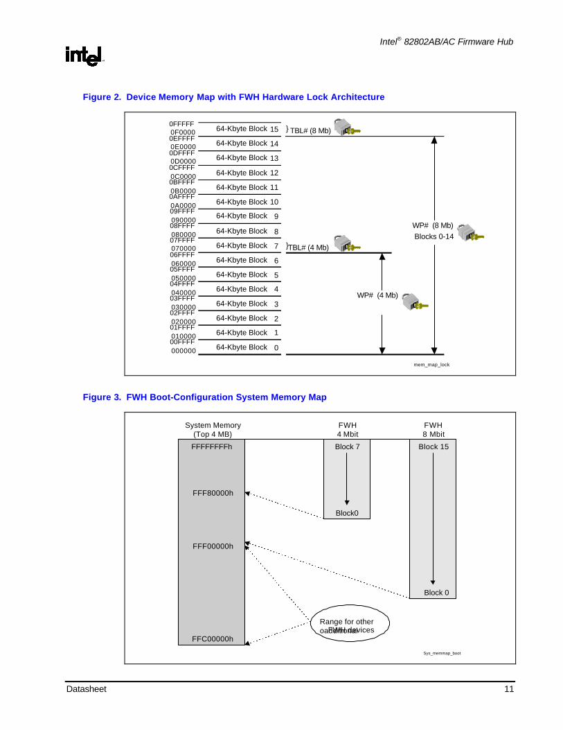
1.2. Nonvolatile Flash Memory Core
The primary feature of the FWH component is a nonvolatile memory core based on Intel® flashtechnology. This high-performance memory array is arranged in eight (4-Mbit device) or sixteen (8-Mbitdevice) 64-KB blocks.
Intel® flash technology enables fast factory programming and low-power designs. Specifically designedfor 3-V systems, this component supports read operations at 3.3 V VCC and block erase and programoperations at 3.3 V and 12 V VPP. The 12 V VPP option yields the fastest program performance, which willincrease factory throughput, but is not recommended for standard in-system FWH operation in theplatform, due to an 80-hr limit for 12 V on the VPP pin over the lifetime of the device, whether or notprogramming is taking place. With the 3.3-V VPP option (recommended for in-system operation), VCC andVPP may be tied together for a simple, low-power 3-V design. In addition to the voltage flexibility, thededicated VPP pin provides complete data protection when VPP ≤≤ VPPLK. Internal VPP detection circuitryautomatically configures the device for block erase and program operations. While current for 12-Vprogramming will be drawn from VPP, 3.3-V programming solutions should design their board such thatVPP draws from the same supply as VCC, and should assume that full programming current may be drawnfrom either pin.
Intel® 82802AB/AC Firmware Hub
R
Datasheet 11
Figure 2. Device Memory Map with FWH Hardware Lock Architecture
15
14
13
12
11
10
9
8
7
6
5
4
3
2
1
0
64-Kbyte Block
64-Kbyte Block
64-Kbyte Block
64-Kbyte Block
64-Kbyte Block
64-Kbyte Block
64-Kbyte Block
64-Kbyte Block
64-Kbyte Block
64-Kbyte Block
64-Kbyte Block
64-Kbyte Block
64-Kbyte Block
64-Kbyte Block
64-Kbyte Block
64-Kbyte Block
TBL# (8 Mb)
TBL# (4 Mb)
WP# (8 Mb)Blocks 0-14
WP# (4 Mb)
mem_map_lock
0FFFFF0F00000EFFFF0E00000DFFFF0D00000CFFFF0C00000BFFFF0B00000AFFFF0A000009FFFF09000008FFFF08000007FFFF07000006FFFF06000005FFFF05000004FFFF04000003FFFF03000002FFFF02000001FFFF01000000FFFF000000
Figure 3. FWH Boot-Configuration System Memory Map
Sys_memmap_boot
System Memory(Top 4 MB)
FFF80000h
FFFFFFFFh
FFF00000h
FFC00000h
FWH4 Mbit
FWH8 Mbit
Block 7
Block0
Block 15
Block 0
Range for otheroadditionalFWH devices

Intel® 82802AB/AC Firmware Hub
R
12 Datasheet
This page is intentionally left blank.

Intel® 82802AB/AC Firmware Hub
R
Datasheet 13
2. Pinout ConfigurationsFigure 4. 32-Lead PLCC Firmware Hub Pinout
Firmware Hub (FWH)32-Lead PLCC0.450" x 0.550"
Top View
RST# VPP
32 31 30
29
28
27
26
25
24
23
22
21
201917 18
1234
5
6
7
8
9
10
11
12
13
14 1615
CLKVCC
FWH2 GND FWH3FWH1
FWH0
ID0
ID1
ID2
ID3
FGPI2 FGPI3 FGPI4
RFU RFU RFU
FGPI1
FGPI0
WP#
TBL#
A/AMux
A/AMux
A/AMux
A/AMux
WE#
IC(V IH)
DQ7
RY/BY#
OE#
GNDa
VCCa
GND
VCC
A5
VPP
A6
A4
VCC
DQ2 GND DQ3 DQ6DQ1 DQ5DQ4
DQ0
R/C#RST# A10A9A8
A7
A3
A2
A1
A0
FWH4
RFU
GNDa
GND
VCCa
IC (V IL)
INIT#
VCC
RFU
Figure 5. 40-Lead TSOP Firmware Hub Pinout
RST#
NC
NCNC
NCNC
VCCVPP
VCCaFWH4INIT#
GNDGND
RFURFU
RFU
ID0ID1ID2ID3
FWH2FWH3
FWH1FWH0
VCCRFU
1234567891011121314151617181920 21
2223242526272829303132
4039383736353433
NC
Firmware Hub (FWH)40-LEAD TSOP10mm x 20mm
TOP VIEW
CLKNC
WP#TBL#
FGPI4
IC (VIL)GNDa
NC
RFU
WE#
NC
NC
NC
IC (V IH)
NC
NC
A10
NC
NC
A9
A8
A7
A6
A5
A4
VCC
VPP
VCCa
RST#
OE#RY/BY#
GND
GND
DQ6
DQ7
DQ5
A0
A1
A2
A3
DQ2
DQ3
DQ1
DQ0
GNDa
VCC
DQ4
NC
R/C#
A/A Mux A/A Mux
FGPI0FGPI1FGPI2FGPI3

Intel® 82802AB/AC Firmware Hub
R
14 Datasheet
2.1. Pin Descriptions
The pin descriptions table details the usage of each device pin. Most pins have dual functionality, withfunctions in both the Firmware Hub and A/A Mux interfaces. The A/A Mux functionality for pins isshown bold italic in the description box for that pin. All pins are designed to be compliant withVCC + 0.3 V max. unless otherwise noted.
Table 1. Pin Descriptions
InterfaceSymbol Type
FWH A/A Mux
Name and Function
IC I X X Interface Configuration Pin. This pin determines which interfaceis used to communicate with the device. When it is held low, theFWH interface is enabled. When it is held High, the A/A Muxinterface is enabled. This pin must be set at power-up or beforereturn from reset, and must not be changed during deviceoperation. This pin is pulled down with an internal resistor ofbetween 20 and 100 kΩ. When the IC is High (A/A Mux mode), thispin will exhibit a leakage current of approximately 200 µA. This pinmay be floated, which will select the FWH mode.
RST# I X X Interface Reset. Valid for both A/A Mux and FWH interfaceoperation. When driven low, RST# inhibits write operations toprovide data protection during power transitions, resets internalautomation, and tri-states pins FWH[3:0] (in FWH interface mode).RST#-high enables normal operation. When exiting from reset, thedevice defaults to read array mode.
INIT# I X Processor Reset. This is a second reset pin for in-system use.This pin is internally combined with the RST# pin. If this pin or RST#is driven low, identical operation is exhibited. This signal is designedto be connected to the chipset INIT signal (Max. voltage depends onthe processor. Do not use 3.3 V).
A/A Mux = OE#
CLK I X 33-MHz Clock for FWH Interface. This input is the same as thatfor the PCI clock and adheres to the PCI specification.
A/A Mux = R/C#
FWH[3:0] I/O X FWH I/Os. I/O communication
A/A Mux = DQ[3:0]
FWH4 I X FWH Input. Input communication
A/A Mux = WE#

Intel® 82802AB/AC Firmware Hub
R
Datasheet 15
InterfaceSymbol Type
FWH A/A Mux
Name and Function
ID[3:0] I X Identification Inputs. These four pins are part of the mechanismthat allows multiple parts to be attached to the same bus. Thestrapping of these pins is used to identify the component. The bootdevice must have ID[3:0] = 0000, and it is recommended that allsubsequent devices use sequential up-count strapping (0001,0010,0011,...). These pins are pulled down with internal resistors,with values between 20 and 100 kΩ, when in the FWH mode. AnyID pins pulled high will exhibit a leakage current of approximately200 µA. Any pins intended to be low may be left to float. In a singleFWH system, all may be left floating.
A/A Mux = A[3:0]
FGPI[4:0] I X
FWH General Purpose Inputs. These individual inputs can beused for additional board flexibility. The state of these pins can beread immediately at boot, through FWH registers. These inputsshould be at their desired state before the start of the PCI clockcycle during which the read is attempted, and they should remain atthe same level until the end of the read cycle. They may only beused for 3.3-V signals. Unused FGPI pins must not be floated.
A/A Mux = A[10:6]
TBL# I X
Top Block Lock. When low, it prevents programming or blockerase to the highest addressable block (7 in a 4-Mbit, 15 in an 8-Mbit component), regardless of the state of the lock register. TBL#-high disables hardware write protection for the top block, thoughregister-based protection still applies. The status of TBL# does notaffect the status of block-locking registers.
A/A Mux = A4
WP# I X
Write Protect. When low, prevents programming or block erase toall but the highest addressable block (0-6 in a 4-Mbit, 0-14 in an 8-Mbit component), regardless of the state of the corresponding lockregisters. WP#-high disables hardware write protection for theseblocks, though register-based protection still applies. The status ofTBL# does not affect the status of block-locking registers.
A/A Mux = A5
A[0:10] I X
Low-Order Address Inputs. Inputs for low-order addressesduring read and write operations. Addresses are internally latchedduring a write cycle. For the A/A Mux interface, these addressesare latched by R/C# and share the same pins as the high-orderaddress inputs.
DQ[0:7] I/O X
Data Input/Outputs. These pins receive data and commandsduring CUI write cycles and transmit data during memory array,status register, and identifier code read cycles. Data pins float tohigh impedance when outputs are disabled. Data is internallylatched during a write cycle.
OE# I X Output Enable. Gates the device’s outputs during a read cycle
R/C# I XRow-Column Address Select. For the A/A Mux interface, thispin determines whether the address pins are pointing to the rowaddresses (A[0:10]) or the column addresses (A[11:19]).
WE# I XWrite Enable. Controls writes to the CUI and array blocks.Addresses and data are latched on the rising edge of the WE#pulse.

Intel® 82802AB/AC Firmware Hub
R
16 Datasheet
InterfaceSymbol Type
FWH A/A Mux
Name and Function
VPP PWR X X
Block Erase/Program Power Supply. For erasing array blocksor programming data. VPP = 3.3 V or 12 V VPP. With VPP ≤ VPPLK,memory contents cannot be altered. Attempting a block erase orprogram with an invalid VPP (see DC Characteristics) will producespurious results and should not be attempted. VPP may only be heldat 12 V for 80 hours over the lifetime of the device.
VCC PWR X X
Device Power Supply. Internal detection automatically configuresthe device for optimized read performance. Do not float any powerpins. With VCC ≤ VLKO, all attempts to write to flash memory areinhibited. Device operations at invalid VCC voltages (see DCCharacteristics) produce spurious results and should not beattempted.
GND PWR X X Ground. Do not float any ground pins.
VCCa PWR X X Analog Power Supply. This supply should share the samesystem supply as VCC.
GNDa PWR X X Analog Ground. Should be tied to same plane as GND.
RFU X
Reserved For Future Use. These pins are reserved for futuregenerations of this product. They may be left disconnected ordriven. If they are driven, the voltage levels should satisfy VIH andVIL requirements.
A/A Mux = DQ[7:4]
NC X XNo Connect. Pin may be driven or floated. If it is driven, the voltagelevels should satisfy VIH and VIL. No connects appear only on the40ld TSOP package.

Intel® 82802AB/AC Firmware Hub
R
Datasheet 17
3. Interface Operation Description
3.1. Read
Memory information, identifier codes, GPI registers or the status register can be read, regardless of theVPP voltage. Commands using the read mode include: reading memory from the array, reading theidentifier codes, reading the status register, reading the lock bit registers, reading the random numbergenerator, reading the GPI registers, and reading the RNG status register. Upon initial device power-up orafter exit from reset, the device automatically resets to read array mode.
3.2. Write
Writes to the memory array’s CUI are initiating by issuing a write through the FWH interface. (See thefollowing information on timing and FWH cycle write protocol specifics.) The CUI does not occupy asingle, specific memory location—any valid address may be given. However, certain commands, such asblock erase, require the address be within the range of the desired address block.
3.3. Output Disable
When the FWH is not selected through a FWH read or write cycle, the FWH interface outputs(FWH[3:0]) are disabled and is placed in a high-impedance state.
3.4. Reset
RST# or INIT# at VIL initiates a device reset. In the read mode, RST# or INIT# low deselects the memory,places output drivers in a high-impedance state, and turns off all internal circuits. RST# or INIT# must beheld low for time tPLPH (A/A Mux and FWH operation). The FWH resets to read array mode upon returnfrom reset, and all blocks are set to default (locked) status (see 4.9.1), regardless of their locked state priorto reset.
During block erase or program, driving RST# or INIT# low will abort the operation underway, in additionto causing a reset latency. Memory contents being altered are no longer valid, since the data may bepartially erased or programmed.
It is important to assert RST# or INIT# during system reset. When the system comes out of reset, it willexpect to read from the memory array of the device. If a system reset occurs with no FWH reset—this ishardware dependent—it is possible that proper processor initialization will not occur. (The FWH memorymay be providing status information instead of memory array data.)

Intel® 82802AB/AC Firmware Hub
R
18 Datasheet
3.5. Operational Effects of Hardware Write-Protect PinsTBL# and WP#
The TBL# and WP# pins on the FWH provide hardware write protect capabilities. The Top Block Lock(TBL#) pin, when held low (active), prevents program or block erase operations in the top-most block ofthe device where critical code can be stored. When TBL# is high, hardware write protection of the topblock is disabled. The Write Protect (WP#) pin has a function similar to TBL#, but affects all remainingblocks. WP# operates independently from TBL# and does not affect the lock status of the top block.
The TBL# and WP# pins must be set to the desired protection state prior to starting a program or eraseoperation, since they are sampled at the beginning of the operation. Changing the state of TBL# or WP#during a program or erase operation may cause unpredictable results.
If the state of TBL# or WP# changes during a program suspend or erase suspend state, the changes tothe device’s locking status do not take place immediately. The suspended operation may be resumed tosuccessfully complete the program or erase operation. The new lock status will take place after theprogram or erase operation completes.
These pins function in combination with the register-based block locking described in Section 4.9. Whenactive, these pins write-protect the appropriate block(s), regardless of the associated block-lockingregisters. (For example, when TBL# is active, writing to the top block is prevented, regardless of the stateof the write-lock bit for the top block’s locking register. In such a case, clearing the write-protect bit in theregister will have no functional effect, even though the register may indicate that the block is no longerlocked. The register may still be set to read-lock the block, if desired.) See Section 4.9 for furtherinformation.

Intel® 82802AB/AC Firmware Hub
R
Datasheet 19
4. Functional Descriptions
When the VPP voltage ≤ VPPLK, read operations from the status register, identifier codes or memory areenabled, but programming and erase functions are disabled. Placing VPPH1/2 on VPP enables successfulblock erase and program operations.
Table 2. Command Definitions
First Bus Cycle Second Bus CycleCommand BusCycles
Required
Notes
Oper. Addr.(1) Data(2) Oper. Addr.(1) Data(2)
Read Array/Reset 1 Write X FFh
Read Identifier Codes ≥ 2 2 Write X 90h Read IA ID
Read Status Register 2 Write X 70h Read X SRD
Clear Status Register 1 Write X 50h
Block Erase 2 3 Write BA 20h Write BA D0h
Program 2 3,4 Write WA 40hor
10h
Write WA WD
Block Erase and ProgramSuspend
1 3 Write X B0h
Block Erase and ProgramResume
1 3 Write X D0h
Note: 1. Key:
X = Any valid address within the deviceIA = Identifier Code AddressBA = Address within the block being erasedWA = Address of memory location to be writtenSRD = Data read from status register.WD = Data to be written at location WAID = Data read from identifier codes
2. Following the Read Identifier Codes command, read operations access manufacturer and device.See Table 4 for the read identifier code data.
3. The block must not be write locked when attempting block erase or program operations. Attemptsto issue a block erase or program to a write-locked block will fail.
4. Either 40h or 10h are recognized by the WSM as the program setup.
Note: Commands other than those shown previously are reserved by Intel for future device implementationsand should not be used.

Intel® 82802AB/AC Firmware Hub
R
20 Datasheet
Table 3. Status Register Definition
7 6 5 4 3 2 1 0
WSMS ESS ES PS VPPS PSS DPS R
Bit Description
7 Write State Machine Status (SR.7). Check SR.7 to determine block erase or program completion.SR.6–0 are invalid while SR.7 = 0.
1 = Ready
0 = Busy
6 Erase Suspend Status (SR.6).
1 = Block erase suspended
0 = Block erase in progress/completed
5 Erase Status (SR.5). If both SR.5 and SR.4 are 1s after a block erase attempt, an improper commandsequence was entered.
1 = Error in block erasure
0 = Successful block erase
4 Program Status (SR.4).
1 = Error in program
0 = Successful program
3 VPP Status (SR.3). SR.3 does not provide a continuous indication of VPP level. The WSM interrogatesand indicates the VPP level only after a block erase or program operation. SR.3 is not guaranteed toreports accurate feedback only when VPP ≠ VPPH1/2.
1 = VPP low detect, operation abort
0 = VPP OK
2 Program Suspend Status (SR.2).
1 = Program suspended
0 = Program in progress/completed
1 Device Protect Status (SR.1). SR.1 does not provide a continuous indication of write-lock bit, TBL#pin or WP# pin values. The WSM interrogates the write-lock bit, TBL# pin or WP# pin only after a blockerase or program operation. Depending on the attempted operation, it informs the system whether ornot the selected block is locked.
1 = Write-lock bit, TBL# pin, or WP# pin Detected, operation abort
0 = Unlock
0 Reserved for future enhancements (SR.0). SR.0 is reserved for future use and should be maskedout when polling the status register.
Intel® 82802AB/AC Firmware Hub
R
Datasheet 21
4.1. Read Array Command
Upon initial device power-up and after exit from reset, the device defaults to the read array mode. Thisoperation can also be initiated by writing the Read Array command. The device remains available forarray reads until another command is written. Once the internal write state machine (WSM) has started ablock erase or program, the device will not recognize the Read Array command until the operation iscompleted, unless the operation is suspended via an Erase Suspend or Program Suspend command. TheRead Array command functions independently of the VPP voltage.
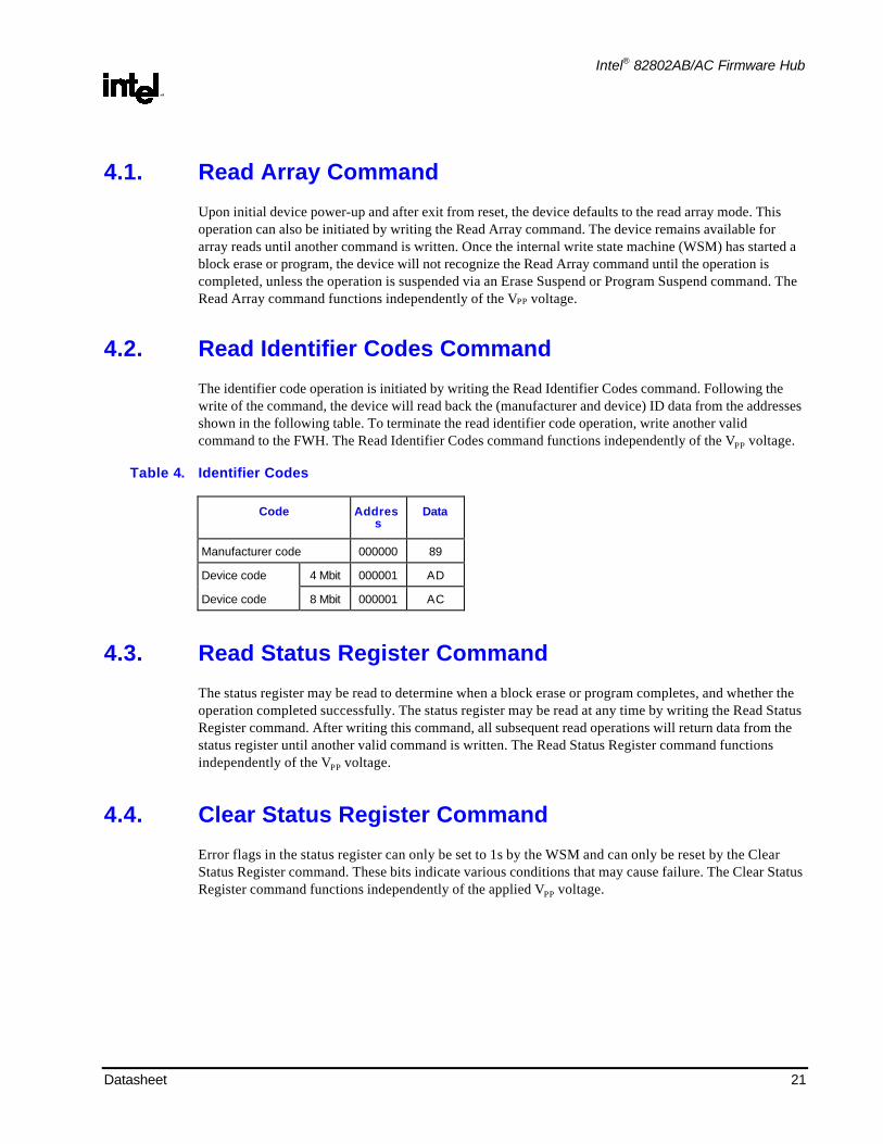
4.2. Read Identifier Codes Command
The identifier code operation is initiated by writing the Read Identifier Codes command. Following thewrite of the command, the device will read back the (manufacturer and device) ID data from the addressesshown in the following table. To terminate the read identifier code operation, write another validcommand to the FWH. The Read Identifier Codes command functions independently of the VPP voltage.
Table 4. Identifier Codes
Code Address
Data
Manufacturer code 000000 89
Device code 4 Mbit 000001 AD
Device code 8 Mbit 000001 AC
4.3. Read Status Register Command
The status register may be read to determine when a block erase or program completes, and whether theoperation completed successfully. The status register may be read at any time by writing the Read StatusRegister command. After writing this command, all subsequent read operations will return data from thestatus register until another valid command is written. The Read Status Register command functionsindependently of the VPP voltage.
4.4. Clear Status Register Command
Error flags in the status register can only be set to 1s by the WSM and can only be reset by the ClearStatus Register command. These bits indicate various conditions that may cause failure. The Clear StatusRegister command functions independently of the applied VPP voltage.

Intel® 82802AB/AC Firmware Hub
R
22 Datasheet
4.5. Block Erase CommandThe erase command operates on one block at a time. This command requires an (arbitrary) address withinthe block to be erased. Recall that erasure changes all block data to FFh. Block preconditioning, erase,and erase verify are handled internally by the WSM, which is transparent to the system. After issuing theerase command, the device automatically outputs status register data when read. When the block erasecompletes, the status register may be checked. If the FWH detects a block erase error, the status registershould be cleared before system software attempts corrective actions. After a block erase, the CUIremains in read status register mode until a new command is issued.
Successful block erasure requires that the corresponding block’s write-lock-bit is cleared, and thecorresponding write-protect pin (TBL# or WP#) is inactive. If a block erase is attempted when the block islocked, the block erase will fail, with the reason for failure in the status register.
Successful block erase only occurs when VPP = VPPH1 or VPPH2. If the erase operation is attempted atVPP ≠≠ VPPH1 or VPPH2, erratic results may occur.
4.6. Program Command
Program command operates on one byte at a time. This command specifies the address and data to beprogrammed. After the CUI receives the command, the WSM takes over, controlling the program andverify algorithms internally. After the program command is written, the device automatically outputs thestatus register data when read. When programming is complete, the status register may be checked. If aprogram error is detected, the status register should be cleared before corrective action is taken by thesoftware. The internal WSM verification error checking only detects 1s that does not successfullyprogram to 0s. The CUI remains in read status register mode until it receives another command.
Reliable programming only occurs when VPP = VPPH1 or VPPH2. If programming is attempted atVPP ≠≠ VPPH1 or VPPH2, erratic results may occur.
Successful program operation also requires that the corresponding block’s write-lock bit be cleared andthat the corresponding write-protect pin (TBL# or WP#) be inactive. If program operation is attemptedwhen the block is locked, the operation will fail.

Intel® 82802AB/AC Firmware Hub
R
Datasheet 23
4.7. Block Erase Suspend Command
The Block Erase Suspend command allows block-erase interruption to read or program data in anotherblock of memory. Once the block erase process starts, writing the Block Erase Suspend commandrequests that the WSM suspend the block erase sequence at a predetermined point in the algorithm. Thedevice outputs status register data when read after the Block Erase Suspend command is written. Pollingthe status register can help determine when the block erase operation was suspended.
After a successful suspend, a Read Array command may be written to read data from a block other thanthe suspended block. A Program command sequence may also be issued during erase suspend toprogram data in blocks other that the block currently in the erase suspend mode.
The other valid commands while block erase is suspended include Read Status Register and Block EraseResume. After a Block Erase Resume command is written, the WSM will continue the block erase process.VPP must remain at VPPH1/2 (the same VPP level initially used for the block erase) while block erase issuspended. RST# or INIT# must also remain at VIH. Block erase cannot resume until program operationsinitiated during block erase suspend have completed.
4.8. Program Suspend Comand
The Program Suspend command allows program interruption to read data in other memory locations.Once the program process starts, writing the Program Suspend command requests that the WSMsuspend the program sequence at a predetermined point in the algorithm. The device continues to outputstatus register data when read after the Program Suspend command is written. Polling status register bitswill help determine when the program operation was suspended.
After a successful suspend, a Read Array command can be written to read data from locations other thanthat which is suspended. The only other valid commands while program is suspended are Read StatusRegister and Program Resume. After Program Resume command is written, the WSM will continue theprogramming process. VPP must remain at VPPH1/2 (the same VPP level used for program) while in programsuspend mode. RST# or INIT# must also remain at VIH.
4.9. Register Based Locking, General-Purpose Input, andRandom Number Generator Registers
A series of registers are available in the FWH to provide software read- and write-locking and GPIfeedback. Also available are the set of control registers for controlling and gathering random numbers.These registers are accessible through standard addressable memory space (see the following table).
It is recommended that the GPI pins be in the desired state before FWH4 is brought low for the beginningof the next bus cycle, and remain in that state until the end of the read.
Intel® 82802AB/AC Firmware Hub
R
24 Datasheet
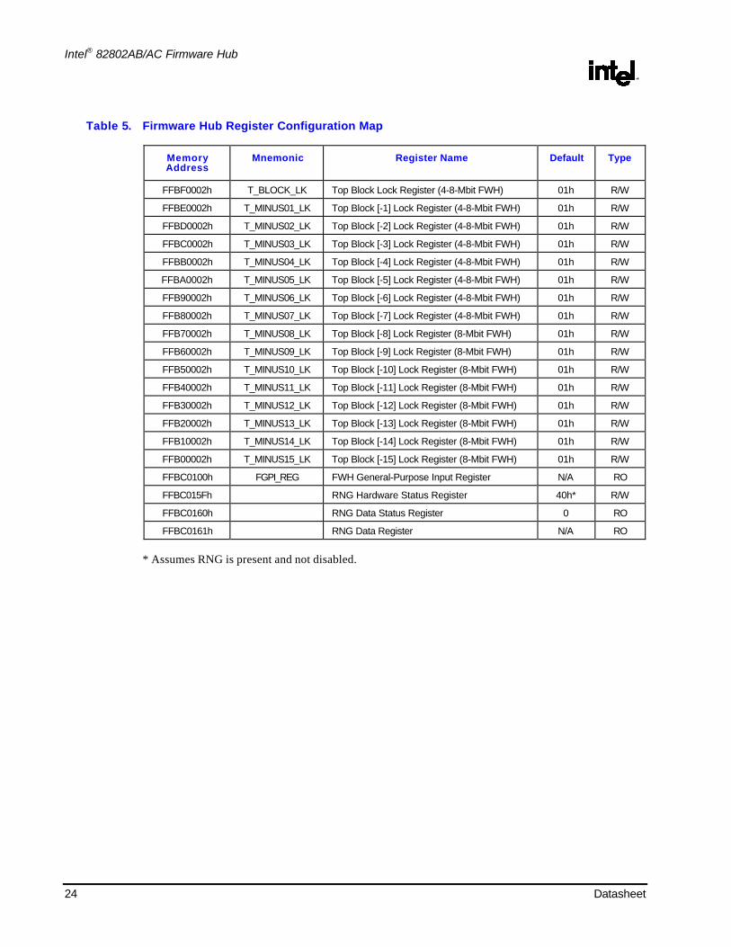
Table 5. Firmware Hub Register Configuration Map
MemoryAddress
Mnemonic Register Name Default Type
FFBF0002h T_BLOCK_LK Top Block Lock Register (4-8-Mbit FWH) 01h R/W
FFBE0002h T_MINUS01_LK Top Block [-1] Lock Register (4-8-Mbit FWH) 01h R/W
FFBD0002h T_MINUS02_LK Top Block [-2] Lock Register (4-8-Mbit FWH) 01h R/W
FFBC0002h T_MINUS03_LK Top Block [-3] Lock Register (4-8-Mbit FWH) 01h R/W
FFBB0002h T_MINUS04_LK Top Block [-4] Lock Register (4-8-Mbit FWH) 01h R/W
FFBA0002h T_MINUS05_LK Top Block [-5] Lock Register (4-8-Mbit FWH) 01h R/W
FFB90002h T_MINUS06_LK Top Block [-6] Lock Register (4-8-Mbit FWH) 01h R/W
FFB80002h T_MINUS07_LK Top Block [-7] Lock Register (4-8-Mbit FWH) 01h R/W
FFB70002h T_MINUS08_LK Top Block [-8] Lock Register (8-Mbit FWH) 01h R/W
FFB60002h T_MINUS09_LK Top Block [-9] Lock Register (8-Mbit FWH) 01h R/W
FFB50002h T_MINUS10_LK Top Block [-10] Lock Register (8-Mbit FWH) 01h R/W
FFB40002h T_MINUS11_LK Top Block [-11] Lock Register (8-Mbit FWH) 01h R/W
FFB30002h T_MINUS12_LK Top Block [-12] Lock Register (8-Mbit FWH) 01h R/W
FFB20002h T_MINUS13_LK Top Block [-13] Lock Register (8-Mbit FWH) 01h R/W
FFB10002h T_MINUS14_LK Top Block [-14] Lock Register (8-Mbit FWH) 01h R/W
FFB00002h T_MINUS15_LK Top Block [-15] Lock Register (8-Mbit FWH) 01h R/W
FFBC0100h FGPI_REG FWH General-Purpose Input Register N/A RO
FFBC015Fh RNG Hardware Status Register 40h* R/W
FFBC0160h RNG Data Status Register 0 RO
FFBC0161h RNG Data Register N/A RO
* Assumes RNG is present and not disabled.

Intel® 82802AB/AC Firmware Hub
R
Datasheet 25
4.9.1. T_BLOCK_LK and T_MINUSxx_LK — Block-LockingRegistersMemory Address: FFBx0002h (x = F-0h)Default Value: 01hAccess: R/WSize: 8 bits (each)
Bit Function
7:3 Reserved
2
Read-Lock
1 = Prevents read operations in the block where set.
0 = Normal operation for reads in the block where clear. This is the default state.
1
Lock-Down
1 = Prevents further set or clear operations to the Write Lock and Read Lock bits. Lock-Down only canbe set, but not cleared. The block will remain locked-down until reset (with RST# or INIT#), or untilthe device is power-cycled.
0 = Normal operation for Write Lock and Read Lock bit altering in the block where clear. This is thedefault state.
0
Write-Lock
1 = Prevents program or erase operations in the block where set. This is the default state.
0 = Normal operation for programming and erase in the block where clear.
Table 6. Register-Based Locking Value Definitions
Data Reserved Data 7:3
Read Lock,Data 2
Lock-Down,Data 1
Write Lock,Data 0
Resulting block state (1).
00h 00000 0 0 0 Full access
01h 00000 0 0 1 Write locked. Default state atpower-up
02h 00000 0 1 0 Locked open (full access lockeddown).
03h 00000 0 1 1 Write-locked down.
04h 00000 1 0 0 Read locked.
05h 00000 1 0 1 Read and write locked.
06h 00000 1 1 0 Read-locked down.
07h 00000 1 1 1 Read- and write-locked down.
Note: The write-lock bit must be set to the desired protection state prior to starting a program or eraseoperation, since it is sampled at the beginning of the operation. Changing the state of the write-lock bitduring a program or erase operation may cause unpredictable results. If the state of the write-lock bitchanges during a program suspend or erase suspend state, changes in the block’s locking status do notoccur immediately. The suspended operation may be resumed successfully. The new lock status will takeplace after the program or erase operation completes. The individual bit functions are described in thefollowing sections.

Intel® 82802AB/AC Firmware Hub
R
26 Datasheet

Intel® 82802AB/AC Firmware Hub
R
Datasheet 27
Write Lock
The default write status of all blocks upon power-up is write-locked. Any program or erase operationsattempted on a locked block will return an error in the status register (indicating block lock). The status ofthe locked block can be changed to unlocked by clearing the write-lock bit, provided the lock-down bitalso is not set. The current write-lock status of a particular block can be determined by reading thecorresponding write-lock bit. The write-lock functions in conjunction with the hardware write-lock pins,TBL# and WP#. When active, these pins take precedence over the register locking function and write-lock the top block or remaining blocks, respectively. Reading this register will not read the state of theTBL# or WP# pin.
Read Lock
The default read status of all blocks upon power-up is read-unlocked. When a block’s read-lock bit is set,data cannot be read from that block. An attempted read from a read-locked block will result in the data00h. (Note that failure is not reflected in the status register.) The read-lock status can be unlocked byclearing the read-lock bit, provided the lock-down bit has not been set. The current read-lock status of aparticular block can be determined by reading the corresponding read-lock bit.
Lock-Down
In the FWH interface mode, the default lock-down status of all blocks upon power-up is not-locked-down. The lock-down bit for any block may be set, but only once, because future attempts to change thatblock-locking register will be ignored. The lock-down bit is cleared only upon a device reset with RST# orINIT#. The current lock-down status of a particular block can be determined by reading thecorresponding lock-down bit. Once a block’s lock-down bit is set, the read- and write-lock bits for thatblock can no longer be modified, and the block is locked-down in its current state of read and writeaccessibility.
4.9.2. General-Purpose Input Register
This register reads the status of the FGPI [4:0] pins on the FWH. Since this is a pass-through register,there is no default value, only the state of the pins at power-up.
4.9.2.1. GPI_REG — General-Purpose Input Register
Memory Address: FFBC0100hDefault Value: N/AAccess: R0Size: 8 bits
Bit Function
7:5 Reserved
4 FGPI[4]. Reads status of general-purpose input pin (PLCC-30/TSOP-7).
3 FGPI[3]. Reads status of general-purpose input pin (PLCC-3/TSOP-15).
2 FGPI[2]. Reads status of general-purpose input pin (PLCC-4/TSOP-16).
1 FGPI[1]. Reads status of general-purpose input pin (PLCC-5/TSOP-17).
0 FGPI[0]. Reads status of general-purpose input pin (PLCC-6/TSOP-18).

Intel® 82802AB/AC Firmware Hub
R
28 Datasheet
4.9.3. Random Number Generator Registers
When enabled and active, the Random Number Generator (RNG) is designed to fill a 32-bit register, a bitat a time, with hardware-generated random numbers. When this register is full, a flag bit in the RNG datastatus register transitions to a 1, indicating that a valid random number is ready to be read. This bit willimmediately reset to 0 upon reading the RNG data register.
The advantages of random numbers over pseudo-random numbers as well as a brief overview of thesimple mathematics of testing RNGs are discussed superficially in the companion document, The Intel®
Platform RNG Tech Brief, which is available online.
4.9.3.1. RNG Hardware Status Register
Memory Address: FFBC015FhDefault Value: 40h, for typical component out of resetAccess: R/W, ROSize: 8 bits
Bit Function
7 Reserved
6 RNG Present—RO. Determines whether or not an RNG is present on this component, or if it has beendisabled.
1 = RNG Present
0 = RNG not present
5:1 Reserved
0 RNG Enabled—R/W. Determines whether the RNG is generating a random number.
1 = RNG enabled
0 = RNG disabled
4.9.3.2. RNG Data Status Register
Memory Address: FFBC016FhDefault Value: 00hAccess: ROSize: 8 bits
Bit Function
7:1 Reserved
0 RNG Output Valid. Determines whether the RNG data register contains a valid random number.
1 = RNG data register contians valid random data
0 = RNG data register contents not valid

Intel® 82802AB/AC Firmware Hub
R
Datasheet 29
4.9.3.3. RNG Data Register
Memory Address: FFBC0161hDefault Value: 40h, for typical component out of resetAccess: R/WSize: 32 bits
Bit Function
7:0 RNG Output: (Should only be used if RNG Data Status Register indicates valid output.)
4.10. Using the Random Number Generator
The Firmware Hub integrates a Random Number Generator that utilizes thermal noise generated as a resultof the inherently random quantum mechanical properties of silicon, in order to modulate a provenhardware RNG design. Internal circuitry is included to enhance the entropy of the output. Since theoutput of the RNG is non-deterministic, it is an excellent choice for cryptography applications, but it alsois a convenient source of random numbers for mathematics, modeling, graphics algorithms, artificialintelligence, entertainment, and many other applications. The fact that it is a component of the platformand may be utilized remotely on a locked-away server makes it an ideal (and much more reliable) source ofentropy for applications that, in the past, have relied exclusively on a key press or other environmentalinput. Several Firmware Hub components may be used in tandem (see the following section) whenadditional RNG bandwidth is required. When not generating new random bits, the RNG circuitry will entera low power state.
4.11. Detecting and Initializing the RNG Device
Before any process attempts to read random data directly from the Firmware Hub RNG device, it shouldexecute a process to verify that a supported RNG device is available for use, enable the device, and verifythe correct functionality. This initialization process is described in a following subsection.
4.11.1. Detecting the RNG Device
The Manufacturer Code and Hardware Status registers are used to determine whether a supported RNGdevice is available on the system.
Step 1: From the system BIOS or using the Read Identifier Codes command, as specified in theIntel® 82802AB/82802AC Firmware Hub (FWH) datasheet, verify the Intel® 82802manufacturer code.
Step 2: If a valid Intel® 82802 FWH is found, then the RNG Present bit (bit 6) of the HardwareStatus register should be checked in order to verify that an RNG device is available.
Note: There is a chance that, even if no RNG device is present, the physical memory locations described abovemay coincidentally match the values expected for an RNG device. For this reason, before random data issent to an application, the device should be exercised to verify that it is indeed an RNG. This can beaccomplished by enabling the device and running an initial test (e.g., FIPS (Federal InformationProcessing Standard) 140-1) before use.

Intel® 82802AB/AC Firmware Hub
R
30 Datasheet
4.11.2. Initializing the RNG Device
Once the RNG device is detected, it must be enabled and should be tested before use.
Step 1: The RNG Enabled bit (bit 0) of the Hardware Status register must be set to enable the RNGdevice.
Step 2: Once the RNG is enabled, an initial read of the RNG Data register should be made to clearany preexisting data from the register.
Step 3: A test (e.g., FIPS 140-1) should be run on the RNG Device. This test will ensure that therewas no error in detecting the device and that the device is functioning properly.
4.11.3. Selecting Appropriate FWH IDs and Densities
It is possible, using different ID strapping, to use multiple FWH components in a system. While the FWHprotocol supports up to 16 FWH devices, the BIOS support, bus loading or the attaching bridge may limitthis number. Note that, regardless of the number of FWH components, the maximum “window” of theFWH array visible at one time is 4 MB (for ICH1) and 8MB for ICH2. The boot device must have an ID (asdetermined by ID [0:3]) of 0. For clarity, it is advisable that subsequent devices use incrementalnumbering.
The most straightforward method of using multiple FWH components is to use devices of equal density.This is the recommended technique.
In special applications, when it is desirable to use multiple FWH components of different densities—ifmultiple RNGs or more GPIs are required, for instance, without the need for greater array space—IDs mustbe chosen such that component memory array spaces do not cross the boundaries delimited by thehighest-capacity device, as illustrated in the following table.
For example, in a design with 8- and 4-Mbit components, the 8-Mbit part must either be first or must beafter enough 4-Mbit parts to add up to a multiple of 8 Mbits.
Yes No Yes
8 Mbits 4 Mbits 4 Mbits
8 Mbits 4 Mbits
4 Mbits 8 Mbits
Biggest is 8 Mbits.

Intel® 82802AB/AC Firmware Hub
R
Datasheet 31
4.11.4. Mapping FWH Devices onto Memory Map
There is 4 MB of available memory space devoted to the FWH. Therefore, the ICH has the ability toselect which FWH device maps into each region of the system address space.
In the existing ICH, the address map is broken up into eight 512-KB segments. The BIOS Select Registerin the ICH is a 32-bit register that contains the needed mapping information, thereby determining whichFWH receives requests from which portion of the address map. For example, in a system with four 8-Mbitdevices, this register would be 00112233h, which is the default power-up state for this register. In asystem with eight 4-Mbit devices, the register must be changed to 01234567h.
Note: The FWH indicated in the most-significant nibble of the register may be shadowed elsewhere in thesystem memory map. The FWH with ID 0 may not be re-mapped.
4.11.5. Paging FWH Devices for Greater Than 4 MB of FWH Memory
In certain applications, even a 4-MB window of flash memory is inadequate. It is possible to exceed thisamount by using a paging scheme. Individual FWH devices may then be “swapped” in and out of systemmemory space. This must be implemented at the BIOS level, to permit modification of the ICH BIOS SelectRegister. A number of paging algorithms may be used successfully with the FWH memory space, usingthe ICH BIOS Select Register. This register, then, determines which FWH device gets mapped into each512 KB “slice” of the system memory map. The 0th FWH (ID=0) may not be remapped. Reference theIntel® 82801AA (ICH) and Intel® 82801AB (ICH0) I/O Controller Hub Datasheet(order number: 290655) for information regarding these components and the BIOS Select Register.
Note: The paging of FWH devices will also “page” features, potentially affecting the visibility or location of theFGPI register (see Section 4.9.2.1) or of an active/ready RNG. When a paging scheme is used, it isrecommended that critical FPGIs be used only on the ID 0 FWH device, which must remain mapped at thetop of memory. Ideally, the RNG driver in a system with more than four FWHs should verify the mappingof FWHs in order to keep track of which RNGs are active and which are present in the memory map. Thereis no convenient way, aside from checking the select register, to determine which IDed FWH is in whichlocation in the memory map.
4.11.6. Programming Multiple FWH Devices
Special considerations must be taken into account when programming multiple FWH devices in-system.Since there is no ID support in the A/A Mux mode, the recommended means of programming multipledevices is either out-of-system programming with standalone PROM programmers or in-systemprogramming using the FWH mode. In cases where programming time is critical or ATE programming isrequired, provisions should be made to isolate the component from its neighboring devices during A/AMux programming, or the other devices should be held in a reset (or otherwise disabled) state untilprogramming of the intended device is complete. Do not switch one component into the A/A Mux mode,thereby leaving the others in the FWH mode.
Intel® 82802AB/AC Firmware Hub
R
32 Datasheet
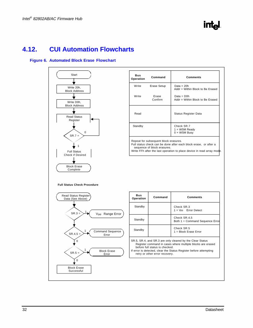
4.12. CUI Automation Flowcharts
Figure 6. Automated Block Erase Flowchart
SR.7 =0
1
Start
Write 20h,Block Address
Write D0h,Block Address
Full StatusCheck if Desired
Block EraseComplete
Full Status Check Procedure
1
Read Status RegisterData (See Above)
1
0
Read StatusRegister
1
0
Command SequenceError
SR.3 =
SR.5 =
SR.4,5 =
Block EraseError
BusOperation Command Comments
Standby
Check SR.4,5Both 1 = Command Sequence ErrorStandby
SR.5, SR.4, and SR.3 are only cleared by the Clear Status Register command in cases where multiple blocks are erased before full status is checked.If error is detected, clear the Status Register before attempting retry or other error recovery.
Check SR.51 = Block Erase Error
Standby
BusOperation Command Comments
Write
Write
Erase Setup
Read
Data = 20hAddr = Within Block to Be Erased
Check SR.71 = WSM Ready0 = WSM Busy
Repeat for subsequent block erasures.Full status check can be done after each block erase, or after a sequence of block erasures.Write FFh after the last operation to place device in read array mode.
Status Register Data
Standby
EraseConfirm
Data = D0hAddr = Within Block to Be Erased
Block EraseSuccessful
Check SR.31 = V Error DetectPP
V Range ErrorPP

Intel® 82802AB/AC Firmware Hub
R
Datasheet 33
This page left intentionally blank

Intel® 82802AB/AC Firmware Hub
R
34 Datasheet
5. Electrical Specifications
5.1. Absolute Maximum Ratings
Case temperature under bias:..............................–10 °C to +85 °C
Storage temperature:...........................................–65 °C to +125 °C
Supply voltage with respect to VSS....................... -0.2 V to 4.1 V
Voltage On Any Pin (except VPP):.... –0.5 V to +VCC + 0.5 V(1,2,5)
VPP voltage: ....................................................–0.5 V to +14.0 V(1,2,4)
Output short-circuit current:............................................100 mA(3)
*WARNING: Stressing the devicebeyond the “Absolute MaximumRatings” may cause permanentdamage. These are stress ratingsonly. Operation beyond the“Operating Conditions” is notrecommended and extended exposurebeyond the “Operating Conditions”may affect device reliability.
Note: 1. All specified voltages are with respect to GND. The minimum DC voltage on the VPP pin is –0.5 V.
During transitions, this level may undershoot to –2.0 V for periods of <20 ns. During transitions,this level may overshoot to VCC + 2.0 V for periods of <20 ns.
2. The maximum DC voltage on VPP may overshoot to +14.0 V for periods of <20 ns.
3. Output shorted for no more than one second. No more than one output is shorted at a time. Thisnote applies only to non-PCI outputs.
4. Connection to supply of VHH is allowed for a maximum cumulative period of 80 hours.
5. Do not violate processor or chipset limitations on the INIT# pin.
5.2. Operating Conditions
Table 7. Temperature and VCC
Symbol Parameter Notes Min. Max. Unit Test Condition
TC Operating temperature 1 0 +85 °C Case temperature
VCC VCC supply voltage (3.3 V ± 0.3 V) 3.0 3.6 V
Note: 1. This temperature requirement differs from the normal commercial operating condition of flash
memories.

Intel® 82802AB/AC Firmware Hub
R
Datasheet 35
5.2.1. Interface DC Input/Output Specifications
Table 8. FWH Interface DC Input/Output Specifications
Symbol Parameter Conditions Min. Max. Units Notes
VIH Input high voltage 0.5 VCC VCC +0.5 V 3
VIH (INIT#) INIT# input high voltage 1.35 VCC +0.5 V 5
VIL Input low voltage -0.5 0.3 VCC V 3
IIL Input leakage current 0 < Vin < VCC ±10 µA 1,4
VOH Output high voltage Iout = -500 µA 0.9 VCC V
VOL Output low voltage Iout = 1500 µA 0.1 VCC V
CIN Input pin capacitance 13 pF
CCLK CLK pin capacitance 3 12 pF
Lpin Recommended pininductance
20 nH 2
Note: 1. Input leakage currents include hi-Z output leakage for all bi-directional buffers with tri-state
outputs.
2. Refer to PCI spec.
3. Inputs are not “5 volt safe.”
4. IIL may be changed on IC and ID pins (up to 200µµA), if pulled against internal pull-downs. Refer tothe pin descriptions (Table 1).
5. Do not violate processor or chipset specifications regarding the INIT# pin voltage.

Intel® 82802AB/AC Firmware Hub
R
36 Datasheet
Table 9. Power Supply Specifications — All Interfaces
Symbol Parameter Conditions Min. Max. Units Notes
VPPH1 VPP voltage 3.0 3.6 V
VPPH2 VPP voltage 11.4 12.6 V
VPPLK VPP lockout voltage 1.5 V
VLKO VCC lockout voltage 1.5 V
ICCSL1 VCC stand-by current
(FWH interface)
Voltage range of all inputs isVIH to VIL, FWH4 = VIH,
VCC = 3.6 V,CLK f = 33 MHz
No internal operations inprogress.
100 µA 2,3,4
ICCSL2 VCC stand-by current
(FWH interface)
FWH4 = VIL
VCC = 3.6 V,CLK f = 33 MHz
No internal operations inprogress.
10 mA 2,3,4
ICCA VCC active current VCC = VCC Max,CLK f = 33 MHz
Any internal operation inprogress,
IOUT = 0mA
67 mA 2,3,5
IPPR VPP read current VPP ≥ VCC 200 µA 2
IPPWE VPP program or VPP = 3.0-3.6 V 40 mA 2
erase current VPP = 11.4-12.6 V 15 mA 2
Note: 1. All currents are RMS, unless otherwise noted. These currents are valid for all packages.
2. VPP
= VCC
3. VIH
= 0.9 VCC
, VIL
= 0.1 VCC
per the PCI output VOH
and VOL
specifications of Table 8.
4. This number is the worst case of IPP
+ ICC memory core + I
CC FWH interface.

Intel® 82802AB/AC Firmware Hub
R
Datasheet 37
5.2.2. Interface AC Input/Output Specifications
Table 10. FWH Interface AC Input/Output Specifications
Symbol Parameter Condition Min. Max. Units Notes
Ioh(AC) Switchingcurrent High
0 < VOUT ≤ 0.3 VCC -12 VCC mA
0.3 VCC < VOUT < 0.9 VCC -17.1 (VCC -VOUT) mA
0.7 VCC < VOUT < VCC Equation C
(Test point) VOUT = 0.7 VCC -32 VCC mA
Iol(AC) Switchingcurrent Low
VCC > VOUT ≥ 0.6 VCC 16 VCC mA
0.6 VCC > VOUT > 0.1 VCC -17.1 (VCC -VOUT) mA
0.18 VCC > VOUT > 0 Equation D
(Test point) VOUT = 0.18 VCC 38 VCC mA
Icl Low clampcurrent
-3 < VIN ≤ -1 -25 + (VIN+1) / 0.015 mA
Ich High clampcurrent
VCC +4 > VIN ≥ VCC+1 25 + (VIN-VCC-1) /0.015
mA
slewr Output riseslew rate
0.2 VCC - 0.6 VCC load 1 4 V/ns 1
slewf Output fallslew rate
0.6 VCC - 0.2 VCC load 1 4 V/ns 1
Note: 1. PCI specification output load is used.

Intel® 82802AB/AC Firmware Hub
R
38 Datasheet
5.2.3. FWH Interface AC Timing Specifications
5.2.3.1. Clock Specification
Table 11. Clock Specification
Symbol Parameter Condition Min. Max. Units Notes
tcyc CLK cycle time 30 ∞ ns 1
thigh CLK high time 11 ns
tlow CLK low time 11 ns
- CLK slew rate Peak-to-peak 1 4 V/ns
- RST# or INIT# slew rate 50 mV/ns 2
Note: 1. PCI components must work with any clock frequency between nominal DC and 33 MHz.
Frequencies less than 16 MHz may be guaranteed by design rather than testing. Refer to the PCIspecificaiton.
2. Applies only to the rising edge of the signal. See Chapter 4 of the PCI electrical specification.
Figure 7. Clock Waveform
0.3 Vcc
0.4 Vcc
0.5 Vcc
0.2 Vcc
0.6 Vcc
T_cyc
T_high
T_low
0.4 Vcc, p-to-p(minimum)

Intel® 82802AB/AC Firmware Hub
R
Datasheet 39
5.2.3.2. Signal Timing Parameters
Table 12. Signal Timing Parameters
Symbol PCISymbol
Parameter Condition
Min. Max. Units
Notes
TCHQV tval CLK to data out 2 11 ns 1
TCHQX ton CLK to active (float to active delay) 2 ns 2
TCHQZ toff CLK to inactive (active to float delay) 28 ns 2
TAVCHTDVCH
tsu Input setup time 7 ns 3
TCHAXTCHDX
th Input hold time 0 ns 3
TVSPL trst Reset active time after power stable 1 ms
TCSPL trst-clk Reset active time after CLK stable 100 µs
TPLQZ trst-off Reset active to output float delay 48 ns 2
Note: 1. Minimum and maximum times have different loads. See PCI spec.
2. For purposes of active/float timing measurements, the Hi-Z or Off state is defined as that in whichthe total current delivered through the component pin is less than or equal to the leakage currentspecification.
3. This parameter applies to any input type (excluding CLK).
Figure 8. Output Timing Parameters
T_off
T_val
V_test
T_on
V_th
V_tl
CLK
FWH[3:0](Valid Output Data)
FWH[3:0](Float Output Data)

Intel® 82802AB/AC Firmware Hub
R
40 Datasheet
Figure 9. Input Timing Parameters
T_su
V_test
V_th
V_tl
CLK
FWH[3:0](Valid Input Data)
T_h
InputsValid
V_max
Table 13. Interface Measurement Condition Parameters
Symbol Value Units Notes
Vth 0.6 VCC V 1
Vtl 0.2 VCC 1
Vtest 0.4 VCC
Vmax 0.4 VCC 1
Input signaledge rate
1 V/ns
Note: 1. The input test environment uses 0.1 VCC of overdrive over VIH and VIL. Timing parameters must
be met with no more overdrive than this. Vmax specifies the maximum peak-to-peak waveformallowed for measuring the input timing. Production testing may use different voltage values, butmust correlate results back to these parameters.
Reset Operations
IHV
ILV
RST# (P)
P1
Table 14. AC Waveform for Reset Operation
# Symbol Parameter Min. Max. Unit Notes
P1(1) tPLPH RST# or INIT# pulse low time (If RST# or INIT# is tiedto VCC, this specification is not applicable.)
100 ns 1
Note: 1. There will be a 20-µs reset latency if a reset procedure is performed during a programming or erase
operation.
Intel® 82802AB/AC Firmware Hub
R
Datasheet 41
5.3. Block Programming Times
Table 15. Programming Times
3.3 V VPP 12 V VPP
Parameter Notes Typ.(1) Max. Typ.(1) Max. Unit
Byte program time 2 17 300 7.0 125 µs
Block program time 2 1.1 4.0 0.5 1.5 sec
Block erase time 2 0.8 6.0 0.3 4.0 sec
Note: 1. Typical values measured at TA = +25°C and nominal voltages.
2. Excludes system-level overhead.
5.4. Firmware Hub Interface
The firmware hub relies on the Firmware Hub interface to communicate with the outside world. Thisinterface consists of four bi-directional signals and one “control” input. The timing and electricalparameters of the FWH interface are similar to those of the LPC interface, to provide compatibilitybetween the interfaces, but differ in cases mentioned earlier in this section (clock pin capacitance), as wellas in certain timing parameters. The ICH has been engineered to accommodate both interfaces, whichallows FWH interface signals to be communicated over the same set of pins as LPC. The FWH interfaceis designed to use an LPC-compatible start cycle, with a reserved cycle type code. This ensures that allLPC devices present on the shared interface will ignore cycles destined for the FWH, without becoming“confused” by the different protocol.
This section contains timing and protocol information for the FWH interface. Note that the FWHinterface is a licensed interface, so the appropriate license must be obtained from Intel for componentssupporting the FWH interface (e.g., ASICs, PLDs).
5.4.1. FWH Interface Cycles
When the FWH interface is active, information is transferred to and from the FWH by a series of “fields,”where each field contains 4 bits of data. Many fields are one clock cycle in length but can be of variablelength, depending upon the nature of the field. Field sequences and contents are strictly defined for readand write operations. The following tables list the field sequences for read and write cycles.
Addresses in this section refer to addresses as seen from the FWH’s “point of view,” so somecalculation will be required to translate these to the actual locations in the memory map (and vice versa).
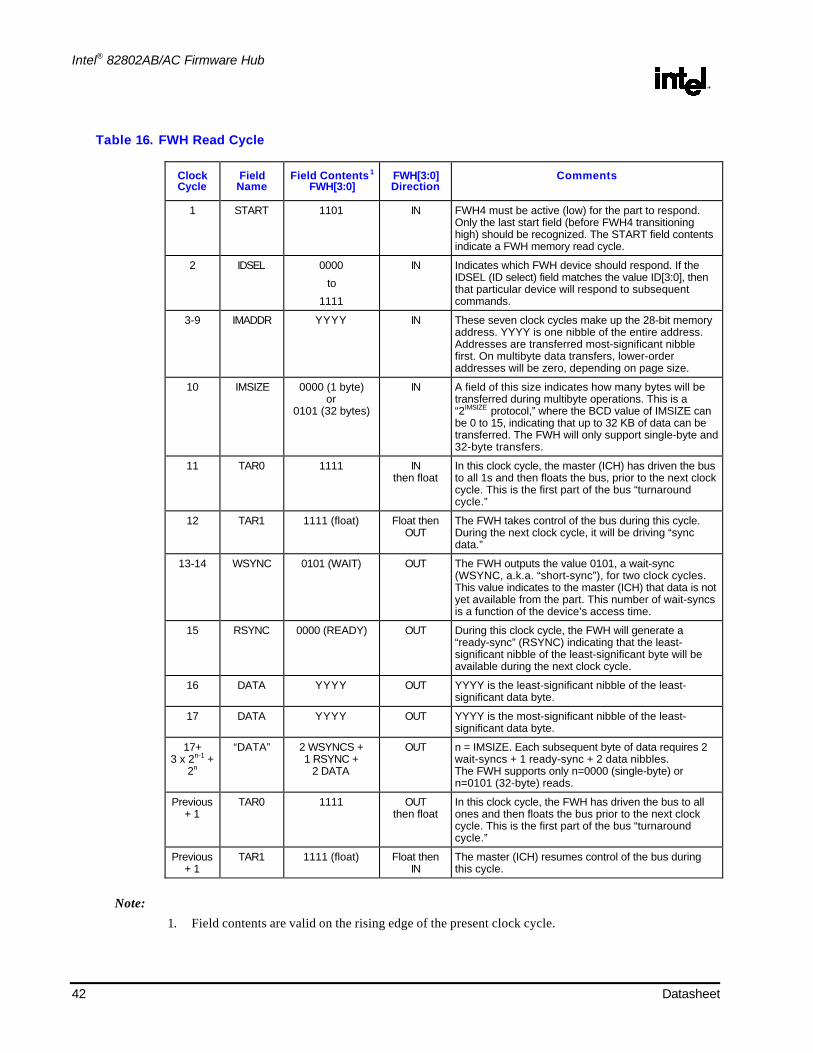
5.4.1.1. Read Cycle Sequence
The firmware hub supports single-byte or multibyte reads. The logic waveforms for these cycles areshown in Table 16 and Figure 11
Intel® 82802AB/AC Firmware Hub
R
42 Datasheet
Table 16. FWH Read Cycle
ClockCycle
FieldName
Field Contents1
FWH[3:0]FWH[3:0]Direction
Comments
1 START 1101 IN FWH4 must be active (low) for the part to respond.Only the last start field (before FWH4 transitioninghigh) should be recognized. The START field contentsindicate a FWH memory read cycle.
2 IDSEL 0000
to
1111
IN Indicates which FWH device should respond. If theIDSEL (ID select) field matches the value ID[3:0], thenthat particular device will respond to subsequentcommands.
3-9 IMADDR YYYY IN These seven clock cycles make up the 28-bit memoryaddress. YYYY is one nibble of the entire address.Addresses are transferred most-significant nibblefirst. On multibyte data transfers, lower-orderaddresses will be zero, depending on page size.
10 IMSIZE 0000 (1 byte)or
0101 (32 bytes)
IN A field of this size indicates how many bytes will betransferred during multibyte operations. This is a“2IMSIZE protocol,” where the BCD value of IMSIZE canbe 0 to 15, indicating that up to 32 KB of data can betransferred. The FWH will only support single-byte and32-byte transfers.
11 TAR0 1111 INthen float
In this clock cycle, the master (ICH) has driven the busto all 1s and then floats the bus, prior to the next clockcycle. This is the first part of the bus “turnaroundcycle.”
12 TAR1 1111 (float) Float thenOUT
The FWH takes control of the bus during this cycle.During the next clock cycle, it will be driving “syncdata.”
13-14 WSYNC 0101 (WAIT) OUT The FWH outputs the value 0101, a wait-sync(WSYNC, a.k.a. “short-sync”), for two clock cycles.This value indicates to the master (ICH) that data is notyet available from the part. This number of wait-syncsis a function of the device’s access time.
15 RSYNC 0000 (READY) OUT During this clock cycle, the FWH will generate a“ready-sync” (RSYNC) indicating that the least-significant nibble of the least-significant byte will beavailable during the next clock cycle.
16 DATA YYYY OUT YYYY is the least-significant nibble of the least-significant data byte.
17 DATA YYYY OUT YYYY is the most-significant nibble of the least-significant data byte.
17+3 x 2n-1 +
2n
“DATA” 2 WSYNCS +1 RSYNC +
2 DATA
OUT n = IMSIZE. Each subsequent byte of data requires 2wait-syncs + 1 ready-sync + 2 data nibbles.The FWH supports only n=0000 (single-byte) orn=0101 (32-byte) reads.
Previous+ 1
TAR0 1111 OUTthen float
In this clock cycle, the FWH has driven the bus to allones and then floats the bus prior to the next clockcycle. This is the first part of the bus “turnaroundcycle.”
Previous+ 1
TAR1 1111 (float) Float thenIN
The master (ICH) resumes control of the bus duringthis cycle.
Note: 1. Field contents are valid on the rising edge of the present clock cycle.

Intel® 82802AB/AC Firmware Hub
R
Datasheet 43
5.4.1.2. Single-Byte Read Waveforms
Figure 10. FWH Single-Byte Read Waveforms
IMADDRSTR
CLK
FWH[3:0]
FWH4
IDS IMS TAR SYNC(3) DATA TAR
5.4.1.3. Write Cycle Sequence
The firmware hub only supports single-byte writes. Each byte represents either the data to be written or avalid flash command. Refer to the waveforms in Figure 11.
Table 17. FWH Write Cycle
ClockCycle
FieldName
FieldContents 1
FWH[3:0]
FWH[3:0]Direction
Comments
1 START 1110 IN FWH4 must be active (low) for the part to respond.Only the last start field (before FWH4 transitioninghigh) should be recognized. The START fieldcontents indicate a FWH memory write cycle.
2 IDSEL 0000to
1111
IN Indicates which FWH device should respond. If theIDSEL (ID select) field matches the value ID[3:0], thenthat particular device will respond to subsequentcommands.
3-9 IMADDR YYYY IN These seven clock cycles make up the 28-bitmemory address. YYYY is one nibble of the entireaddress. Addresses are transferred most-significantnibble first.
10 IMSIZE 0000 (1 byte) IN This size field indicates how many bytes will betransferred during multibyte operations. This is a“2IMSIZE protocol,” where the BCD value of IMSIZEcan be 0 to 15, indicating that up to 32 KB of datacan be transferred. The FWH only supports single-byte writes.
11 DATA YYYY IN This field is the least-significant nibble of the databyte. This data is either the data to be programmedinto the flash memory or any valid flash command.
12 DATA YYYY IN This field is the most-significant nibble of the databyte.
13 TAR0 1111 INthen float
In this clock cycle, the master (ICH) has driven thebus to all 1s and then floats the bus prior to the nextclock cycle. This is the first part of the bus“turnaround cycle.”
14 TAR1 1111 (float) Float thenOUT
The FWH takes control of the bus during this cycle.During the next clock cycle it will be driving the“sync” data.

Intel® 82802AB/AC Firmware Hub
R
44 Datasheet
ClockCycle
FieldName
FieldContents 1
FWH[3:0]
FWH[3:0]Direction
Comments
15 RSYNC 0000 OUT The FWH outputs the values 0000, indicating that ithas received data or a flash command.
16 TAR0 1111 OUTthen float
In this clock cycle, the FWH has driven the bus to all1s and then floats the bus prior to the next clockcycle. This is the first part of the bus “turnaroundcycle.”
17 TAR1 1111 (float) Float thenIN
The master (ICH) resumes control of the bus duringthis cycle.
Note: 1. Field contents are valid on the rising edge of the present clock cycle.
5.4.1.4. Write Waveforms
Figure 11. Write Waveforms
IMADDRSTR
CLK
FWH[3:0]
FWH4
IDS IMS TAR SYNC
DATA TAR
5.4.1.5. Response To Invalid Fields
During FWH operations, the FWH will not explicitly indicate that it has received invalid field sequences.The response to specific invalid fields or sequences is as follows:
• Address out of range: The FWH address sequence is 7 fields long (28 bits), but only the last fiveaddress fields (20 bits) will be decoded by an 8-Mbit FWH. (For a 4-Mbit density, the most-significant bit (FWH3) in the third address field also will be ignored.) The FWH will respond to theselower addresses, regardless of the value of the more-significant address bits. Address A22 has thespecial function of directing reads and writes to the flash core (A22 = 1) or to the register space (A22= 0).
• Invalid IMSIZE field: If the FWH receives an invalid size field during a read or write operation, theinternal state machine will reset and no operation will be attempted. The FWH will generate noresponse of any kind in this situation. Invalid-size fields for a read cycle are anything but 0000.Invalid-size fields for a write cycle are anything but 0000. When accessing register space, invalidfield sizes are anything but 0000.
• Non-page-aligned address: The FWH assumes that multibyte read addresses are page aligned (i.e.,for a 32-byte access, the lower 5 address bits will be zero). If they are not zero, the first byte of datareturned by the FWH will correspond to that explicit address, and subsequent data will be as if thefirst address was indeed page aligned.
Once valid START, IDSEL, and IMSIZE fields are received, the FWH always will respond to subsequentinputs as if they were valid. As long as the states of FWH [3:0] and FWH4 are known, the response ofthe FWH to signals received during the FWH cycle should be predictable. The FWH will make no attemptto check the validity of incoming flash operation commands.
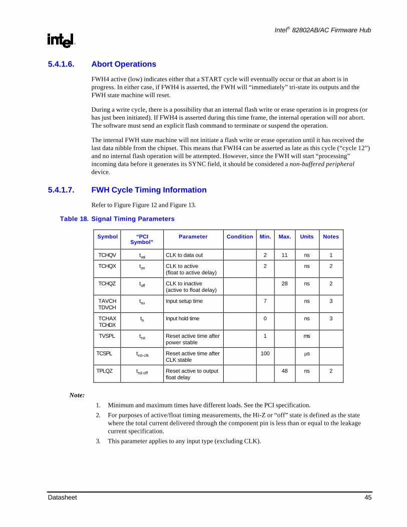
Intel® 82802AB/AC Firmware Hub
R
Datasheet 45
5.4.1.6. Abort Operations
FWH4 active (low) indicates either that a START cycle will eventually occur or that an abort is inprogress. In either case, if FWH4 is asserted, the FWH will “immediately” tri-state its outputs and theFWH state machine will reset.
During a write cycle, there is a possibility that an internal flash write or erase operation is in progress (orhas just been initiated). If FWH4 is asserted during this time frame, the internal operation will not abort.The software must send an explicit flash command to terminate or suspend the operation.
The internal FWH state machine will not initiate a flash write or erase operation until it has received thelast data nibble from the chipset. This means that FWH4 can be asserted as late as this cycle (“cycle 12”)and no internal flash operation will be attempted. However, since the FWH will start “processing”incoming data before it generates its SYNC field, it should be considered a non-buffered peripheraldevice.
5.4.1.7. FWH Cycle Timing Information
Refer to Figure Figure 12 and Figure 13.
Table 18. Signal Timing Parameters
Symbol “PCISymbol”
Parameter Condition Min. Max. Units Notes
TCHQV tval CLK to data out 2 11 ns 1
TCHQX ton CLK to active(float to active delay)
2 ns 2
TCHQZ toff CLK to inactive(active to float delay)
28 ns 2
TAVCHTDVCH
tsu Input setup time 7 ns 3
TCHAXTCHDX
th Input hold time 0 ns 3
TVSPL trst Reset active time afterpower stable
1 ms
TCSPL trst-clk Reset active time afterCLK stable
100 µs
TPLQZ trst-off Reset active to outputfloat delay
48 ns 2
Note: 1. Minimum and maximum times have different loads. See the PCI specification.
2. For purposes of active/float timing measurements, the Hi-Z or “off” state is defined as the statewhere the total current delivered through the component pin is less than or equal to the leakagecurrent specification.
3. This parameter applies to any input type (excluding CLK).
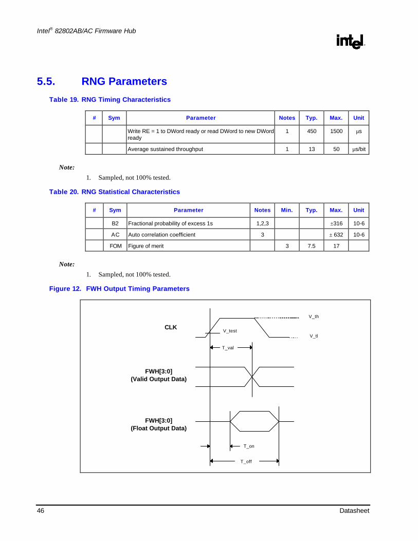
Intel® 82802AB/AC Firmware Hub
R
46 Datasheet
5.5. RNG Parameters
Table 19. RNG Timing Characteristics
# Sym Parameter Notes Typ. Max. Unit
Write RE = 1 to DWord ready or read DWord to new DWordready
1 450 1500 µs
Average sustained throughput 1 13 50 µs/bit
Note: 1. Sampled, not 100% tested.
Table 20. RNG Statistical Characteristics
# Sym Parameter Notes Min. Typ. Max. Unit
B2 Fractional probability of excess 1s 1,2,3 ±316 10-6
AC Auto correlation coefficient 3 ± 632 10-6
FOM Figure of merit 3 7.5 17
Note: 1. Sampled, not 100% tested.
Figure 12. FWH Output Timing Parameters
T_off
T_val
V_test
T_on
V_th
V_tl
CLK
FWH[3:0](Valid Output Data)
FWH[3:0](Float Output Data)
Intel® 82802AB/AC Firmware Hub
R
Datasheet 47
Figure 13. FWH Input Timing Parameters
T_su
V_test
V_th
V_tl
CLK
FWH[3:0](Valid Input Data)
T_h
InputsValid
V_max
Intel® 82802AB/AC Firmware Hub
R
48 Datasheet
6. PROM Programming Specifications
6.1. Programming (“A/A Mux”) Mode Operation
The Intel® 82802 is designed to offer a parallel programming mode for faster factory programming. Thismode, called the A/A Mux mode, is selected by IC high. The IC pin is pulled down internally in the Intel®
82802, so it should be expected that a modest current will be drawn. (See the pin descriptions in Table 1for further information.)
The following information applies only to the Intel® 82802 when in the A/A Mux mode. Informationregarding the FWH mode (i.e., the standard operating mode) is provided in earlier chapters of thisdocument
6.2. Bus Operation
All A/A mux bus cycles can be conformed to operate on most automated test equipment and PROMprogrammers.
6.2.1. Output Disable/Enable
With OE# at the logic-high level (VIH), the device outputs are disabled. Output pins DQ0–DQ7 are placedin the high-impedance state. With OE# at the logic-low level (VIL), the device outputs are enabled. Outputpins DQ0–DQ7 are placed in the output-drive state.
6.2.2. Row/Column Addresses
R/C# is the A/A mux control pin used to latch row (A0–A10) and column addresses (A11–A18/4 Mbits,or A[11:19] /8 Mbits). R/C# latches row addresses on the falling edge and column addresses on the risingedge.
6.2.3. Read Operation
Block information, identifier codes or status register data can be read independently of the VPP voltage.The first task is to write the appropriate read-mode command (Read Array, Read Identifier Codes or ReadStatus Register) to the CUI. Upon initial device power-up or after exit from reset, the device defaults tothe read array mode. Four control pins dictate the data flow into and out of the component: R/C#, OE#,WE#, and RST#. R/C# is the A/A mux control pin used to latch row and column addresses. OE#, the dataoutput control pin (DQ0–DQ7), drives the selected memory data onto the I/O bus, when active. WE# andRST# must be at VIH.
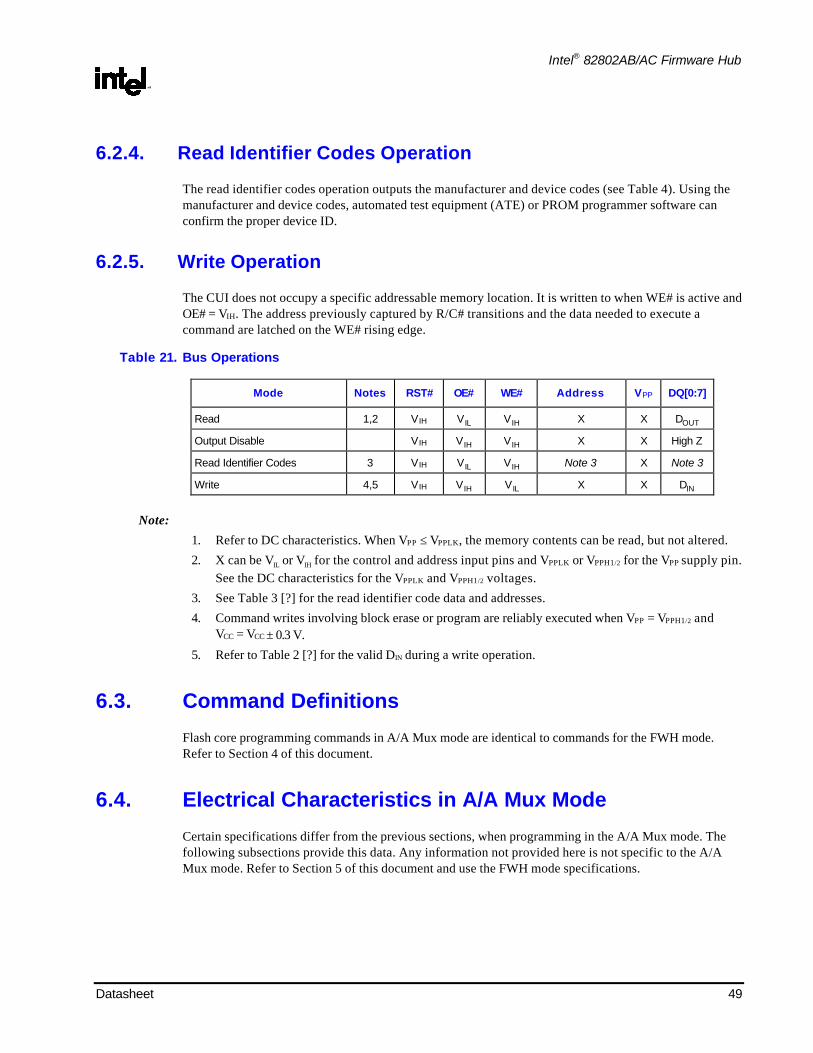
Intel® 82802AB/AC Firmware Hub
R
Datasheet 49
6.2.4. Read Identifier Codes Operation
The read identifier codes operation outputs the manufacturer and device codes (see Table 4). Using themanufacturer and device codes, automated test equipment (ATE) or PROM programmer software canconfirm the proper device ID.
6.2.5. Write Operation
The CUI does not occupy a specific addressable memory location. It is written to when WE# is active andOE# = VIH. The address previously captured by R/C# transitions and the data needed to execute acommand are latched on the WE# rising edge.
Table 21. Bus Operations
Mode Notes RST# OE# WE# Address VPP DQ[0:7]
Read 1,2 VIH VIL VIH X X DOUT
Output Disable VIH VIH VIH X X High Z
Read Identifier Codes 3 VIH VIL VIH Note 3 X Note 3
Write 4,5 VIH VIH VIL X X DIN
Note: 1. Refer to DC characteristics. When VPP ≤ VPPLK, the memory contents can be read, but not altered.
2. X can be VIL or VIH for the control and address input pins and VPPLK or VPPH1/2 for the VPP supply pin.See the DC characteristics for the VPPLK and VPPH1/2 voltages.
3. See Table 3 [?] for the read identifier code data and addresses.
4. Command writes involving block erase or program are reliably executed when VPP = VPPH1/2 andVCC = VCC ± 0.3 V.
5. Refer to Table 2 [?] for the valid DIN during a write operation.
6.3. Command Definitions
Flash core programming commands in A/A Mux mode are identical to commands for the FWH mode.Refer to Section 4 of this document.
6.4. Electrical Characteristics in A/A Mux Mode
Certain specifications differ from the previous sections, when programming in the A/A Mux mode. Thefollowing subsections provide this data. Any information not provided here is not specific to the A/AMux mode. Refer to Section 5 of this document and use the FWH mode specifications.

Intel® 82802AB/AC Firmware Hub
R
50 Datasheet
6.4.1. Reset Operations
# Symbol Parameter Notes Min. Max. Unit
P1 tPLPH RST# pulse low time (If RST# is tied to VCC, thisspecification is not applicable.)
100 ns
P2 tPLRH RST# low to reset during block erase or program 1, 2 20 µs
Note: 1. If RST# is asserted when the WSM is not busy (RY/BY# = ‘1’), the reset will complete within 100
ns.
2. A reset time, tPHAV, is required from the latter of RY/BY# or RST# going high until outputs are valid.
6.4.2. AC Waveforms for Reset Operations
IHV
ILVRST# (P)
IHV
ILVRY/BY# (R)
P1
P2
6.4.3. A/A Mux Read-Only Operations (1,3)
# Symbol Parameter Notes Min. Max. Unit
R1 tAVAV Read cycle time 250 ns
R2 tAVCL Row address setup to R/C# low 50 ns
R3 tCLAX Row address hold from R/C# low 50 ns
R4 tAVCH Column address setup to R/C# high 50 ns
R5 tCHAX Column address hold from R/C# high 50 ns
R6 tCHQV R/C# high to output delay 2 150 ns
R7 tGLQV OE# low to output delay 2 50 ns
R8 tPHAV RST# high to row address setup 1 µs
R9 tGLQX OE# low to output in low Z 0 ns
R10 tGHQZ OE# high to output in high Z 50 ns
R11 tQXGH Output hold from OE# high 0 ns
Note: 1. See the AC input/output reference waveform for the maximum allowable input slew rate.
2. OE# may be delayed up to tCHQV – tGLQV after the rising edge of R/C# without affecting tCHQV.
3. Tc = 0 °C to + 85 °C, 3.3 V ± 0.3 V VCC

Intel® 82802AB/AC Firmware Hub
R
Datasheet 51
Figure 14. A/A Mux Read Timing Diagram
ADDRESSES (A)
R/C# (C)
VIH
VIL
VIH
VIL
Row AddressStable
Column AddressStable
WE# (W)VIH
VIL
OE# (G)VIH
VIL
RP# (P)
VIH
VIL
DATA (D/Q)
VOH
VOL
High Z High ZData Valid
R7
R9
x
x
R8
R2 R5
R3 R4R6
R1
R11
R10
x
x
Next AddressStable

Intel® 82802AB/AC Firmware Hub
R
52 Datasheet
6.4.4. A/A Mux Write Operations (1,2)
# Symbol Parameter Notes Min. Max. Units
W1 tPHWL RP# high recovery to WE# low 1 µs
W2 tWLWH Write pulse width low 100 ns
W3 tDVWH Data setup to WE# high 1 50 ns
W4 tWHDX Data hold from WE# high 1 5 ns
W5 tAVCL Row address setup to R/C# low 1 50 ns
W6 tCLAX Row address hold from R/C# low 1 50 ns
W7 tAVCH Column address setup to R/C# high 1 50 ns
W8 tCHAX Column address hold from R/C# high 1 50 ns
W9 tWHWL Write pulse width high 100 ns
W10 tCHWH R/C# high setup to WE# high 50 ns
W11 tVPWH VPP1,2 setup to WE# high 100 ns
W12 tWHGL Write recovery before read 150 ns
W13 tWHRL WE# high to RY/BY# going low 0 ns
W14 tQVVL VPP1,2 hold from valid SRD, RY/BY# high 0 ns
Note: 1. Refer to Table 6-28 [?] for valid AIN and DIN for block erase or program or other commands.
2. Tc = 0 °C to + 85 °C, 3.3 V ± 0.3 V VCC
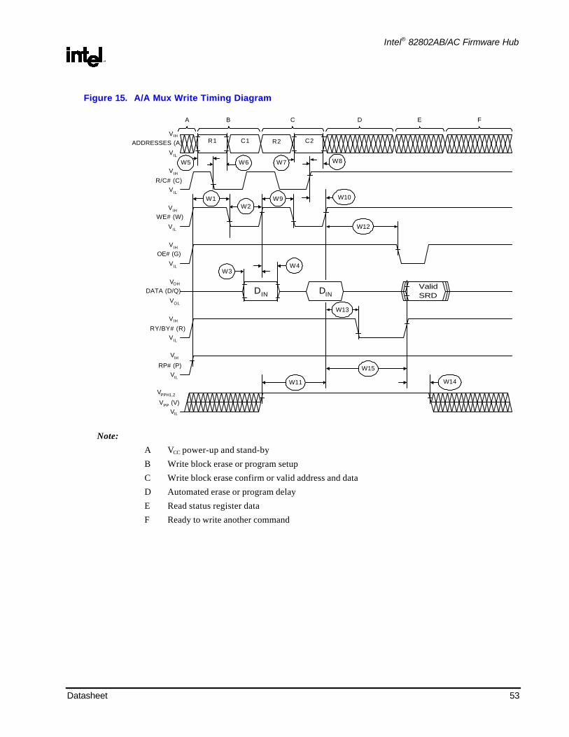
Intel® 82802AB/AC Firmware Hub
R
Datasheet 53
Figure 15. A/A Mux Write Timing Diagram
ADDRESSES (A)
R/C# (C)
VIH
VIL
VIH
VIL
WE# (W)VIH
VIL
RY/BY# (R)
VIH
VIL
VPP (V)
VPPH1,2
VIL
RP# (P)
VIH
VIL
R1 C1 R2 C2
OE# (G)VIH
VIL
DATA (D/Q)VOH
VOL
W5 W7W6 W8
W10W1W2
W9
W3W4
W11 W14
W12
W13
W15
ValidSRDDINDIN
A B C D E F
Note: A VCC power-up and stand-by
B Write block erase or program setup
C Write block erase confirm or valid address and data
D Automated erase or program delay
E Read status register data
F Ready to write another command