Intel 80303 and 80302 I/O Processors - cpu-galaxy.at rom eprom/other_intel_chips/other_intel... ·...
38
Intel ® 80303 and 80302 I/O Processors Specification Update May 6, 2003 Notice: The Intel ® 80303 and Intel ® 80302 I/O Processors processor may contain design defects or errors known as errata. Characterized errata that may cause the product’s behavior to deviate from pubished specifications are documented in this specification update. Order Number: 273355-010
Transcript of Intel 80303 and 80302 I/O Processors - cpu-galaxy.at rom eprom/other_intel_chips/other_intel... ·...

Intel® 80303 and 80302 I/O ProcessorsSpecification Update
May 6, 2003
Notice: The Intel® 80303 and Intel® 80302 I/O Processors processor may contain design defects or errors known as errata. Characterized errata that may cause the product’s behavior to deviate from pubished specifications are documented in this specification update.
Order Number: 273355-010

Intel® 80303 and 80302 I/O Processors Specification Update
INFORMATION IN THIS DOCUMENT IS PROVIDED IN CONNECTION WITH INTEL® PRODUCTS. NO LICENSE, EXPRESS OR IMPLIED, BY ESTOPPEL OR OTHERWISE, TO ANY INTELLECTUAL PROPERTY RIGHTS IS GRANTED BY THIS DOCUMENT. EXCEPT AS PROVIDED IN INTEL'S TERMS AND CONDITIONS OF SALE FOR SUCH PRODUCTS, INTEL ASSUMES NO LIABILITY WHATSOEVER, AND INTEL DISCLAIMS ANY EXPRESS OR IMPLIED WARRANTY, RELATING TO SALE AND/OR USE OF INTEL PRODUCTS INCLUDING LIABILITY OR WARRANTIES RELATING TO FITNESS FOR A PARTICULAR PURPOSE, MERCHANTABILITY, OR INFRINGEMENT OF ANY PATENT, COPYRIGHT OR OTHER INTELLECTUAL PROPERTY RIGHT.
Intel products are not intended for use in medical, life saving, life sustaining applications.
Intel may make changes to specifications and product descriptions at any time, without notice.
Designers must not rely on the absence or characteristics of any features or instructions marked "reserved" or "undefined." Intel reserves these for future definition and shall have no responsibility whatsoever for conflicts or incompatibilities arising from future changes to them.
The Intel® 80303 and Intel® 80302 I/O Processors may contain design defects or errors known as errata which may cause the product to deviate from published specifications. Current characterized errata are available on request.
Intel® internal code names are subject to change.
Contact your local Intel sales office or your distributor to obtain the latest specifications and before placing your product order.
Copies of documents which have an ordering number and are referenced in this document, or other Intel literature may be obtained by calling 1-800-548-4725 or by visiting Intel's website at http://www.intel.com.
Copyright© Intel Corporation, 2003
AlertVIEW, i960, AnyPoint, AppChoice, BoardWatch, BunnyPeople, CablePort, Celeron, Chips, Commerce Cart, CT Connect, CT Media, Dialogic, DM3, EtherExpress, ETOX, FlashFile, GatherRound, i386, i486, iCat, iCOMP, Insight960, InstantIP, Intel, Intel logo, Intel386, Intel486, Intel740, IntelDX2, IntelDX4, IntelSX2, Intel ChatPad, Intel Create&Share, Intel Dot.Station, Intel GigaBlade, Intel InBusiness, Intel Inside, Intel Inside logo, Intel NetBurst, Intel NetStructure, Intel Play, Intel Play logo, Intel Pocket Concert, Intel SingleDriver, Intel SpeedStep, Intel StrataFlash, Intel TeamStation, Intel WebOutfitter, Intel Xeon, Intel XScale, Itanium, JobAnalyst, LANDesk, LanRover, MCS, MMX, MMX logo, NetPort, NetportExpress, Optimizer logo, OverDrive, Paragon, PC Dads, PC Parents, Pentium, Pentium II Xeon, Pentium III Xeon, Performance at Your Command, ProShare, RemoteExpress, Screamline, Shiva, SmartDie, Solutions960, Sound Mark, StorageExpress, The Computer Inside, The Journey Inside, This Way In, TokenExpress, Trillium, Vivonic, and VTune are trademarks or registered trademarks of Intel Corporation or its subsidiaries in the United States and other countries.
*Other names and brands may be claimed as the property of others.

Intel® 80303 and 80302 I/O Processors Specification Update 3
Contents
Revision History ......................................................................................... 5
Preface....................................................................................................... 7
Summary Table of Changes....................................................................... 8
Identification Information.......................................................................... 14
Errata ....................................................................................................... 16
Specification Changes ............................................................................. 23
Specification Clarifications ....................................................................... 25
Documentation Changes ......................................................................... 28

4 Intel® 80303 and 80302 I/O Processors Specification Update
This Page Intentionally Left Blank
Intel® 80303 and 80302 I/O Processors Specification Update 5
Revision History
Revision Historysc
Date Version Description
05/01/03 010Added Errata 2.
Revised Specification Clarifications 4, 7 and 8.
08/27/02 009Reworded Specification Clarification 4.
Added Specification Clarifications 7 and 8.
11/15/01 008Added Specification Clarifications 5 and 6.
Added Document Changes 32 and 33.
08/22/01 007Added Specification Clarification 4.
Added Document Changes 30 and 31.
04/24/01 006
Added Document Changes 25 through 29.
Revised Device ID Registers “A-2” Revision ID Registers data.
Added Note to Device ID Registers.
04/02/01 005 Added Specification Clarification 3.
03/22/01 004
Added Errata 1.
Added Specification Change 1.
Added Specification Clarifications 1 and 2.
Added Document Changes 13 through 24.
Updated Die Details Table and Device ID Registers for A-2 step.
02/23/01 003 Die Details and Device ID Registers tables, corrected stepping A-0 to A-1.
08/2000 002
Updated Die Details Table.
Revised Device ID Registers Table.
Added Document Changes 1 through 12.
06/2000 001 This is the new Specification Update document. It contains all identified errata published prior to this date.
Preface
6 Intel® 80303 and 80302 I/O Processors Specification Update
Preface
This document is an update to the specifications contained in the Affected Documents/Related Documents table below. This document is a compilation of device and documentation errata, specification clarifications and changes. It is intended for hardware system manufacturers and software developers of applications, operating systems, or tools.
Information types defined in Nomenclature are consolidated into the specification update and are no longer published in other documents.
This document may also contain information that was not previously published.
Affected Documents/Related Documents
Nomenclature
Errata are design defects or errors. These may cause the Intel® 80303 and Intel® 80302 I/O Processors behavior to deviate from published specifications. Hardware and software designed to be used with any given stepping must assume that all errata documented for that stepping are present on all devices.
Specification Changes are modifications to the current published specifications. These changes will be incorporated in any new release of the specification.
Specification Clarifications describe a specification in greater detail or further highlight a specification’s impact to a complex design situation. These clarifications will be incorporated in any new release of the specification.
Documentation Changes include typos, errors, or omissions from the current published specifications. These will be incorporated in any new release of the specification.
Note: Errata remain in the specification update throughout the product’s lifecycle, or until a particular stepping is no longer commercially available. Under these circumstances, errata removed from the specification update are archived and available upon request. Specification changes, specification clarifications and documentation changes are removed from the specification update when the appropriate changes are made to the appropriate product specification or user documentation (datasheets, manuals, etc.).
Title Order #
Intel® 80303 I/O Processor Developer’s Manual 273353
Intel® 80303 I/O Processor Data Sheet 273358
Intel® 80303 I/O Processor Design Guide 273308

Intel® 80303 and 80302 I/O Processors Specification Update 7
Summary Table of Changes
Summary Table of Changes
The following table indicates the errata, specification changes, specification clarifications, or documentation changes which apply to the Intel® 80303 and Intel® 80302 I/O Processors product. Intel may fix some of the errata in a future stepping of the component, and account for the other outstanding issues through documentation or specification changes as noted. This table uses the following notations:
Codes Used in Summary Table
Stepping
X: Errata exists in the stepping indicated. Specification Change or Clarification that applies to this stepping.
(No mark)
or (Blank box): This erratum is fixed in listed stepping or specification change does not apply to listed stepping.
Page
(Page): Page location of item in this document.
Status
Doc: Document change or update will be implemented.
Fix: This erratum is intended to be fixed in a future step of the component.
Fixed: This erratum has been previously fixed.
NoFix: There are no plans to fix this erratum.
Eval: Plans to fix this erratum are under evaluation.
Row
Change bar to left of table row indicates this erratum is either new or modified from the previous version of the document.

Summary Table of Changes
8 Intel® 80303 and 80302 I/O Processors Specification Update
Errata
No.Steppings
Page Status ErrataA-0 A-1 A-2
1 X X X 12 NoFix Single-bit and Multi-bit Error Reporting Cannot Be Individually Enabled by ECC Control Register
2 X X X 12 NoFix Instruction Sequence Can Scoreboard a Register Indefinitely
Specification Changes
No.Steppings
Page Status Specification ChangesA-2 #-# #-#
1 X 14 Doc Summary of the Intel® 80302 I/O Processor
Specification Clarifications
No.Steppings
Page Status Specification ClarificationsA-0 A-1 A-2
1 X X X 15 Doc ECC is Always Enabled
2 X X X 15 Doc 32-bit SDRAM is Not Supported
3 X X X 15 Doc Non-Battery Backup Systems
4 X X X 15 Doc POCCDR and SOCCDR Functionality
5 X X X 15 Doc ‘Bus Hold’ Devices on the RAD Bus
6 X X X 16 Doc SREQ64# Functionality
7 X X X 16 Doc PCI Local Bus Specification, Revision 2.3 Compliancy
8 X X X 16 Doc DMA and AAU End of Chain Functionality

Intel® 80303 and 80302 I/O Processors Specification Update 9
Summary Table of Changes
Documentation ChangesNo. Document Revision Page Status Documentation Changes
1 272353-001 17 Doc Title Page revision number
2 272353-001 17 Doc Figure 9-3 on pg 9-9 did not print correctly
3 272353-001 18 Doc Figure 13-22 on pg 13-40 did not print correctly
4 272353-001 18 Doc Figure 13-18, pg 13-35
5 272353-001 19 Doc Figure 15-2 on pg 15-3 did not print correctly
6 272353-001 20 Doc Incorrect Vendor ID in ATU register
7 272353-001 20 Doc Section 23.2 on pg 23-2 has incorrect text
8 272353-001 21 Doc Table 24-4 on pg 24-8 is incorrect
9 272353-001 31 Doc Figure 25-1 on pg 25-1 has incorrect data
10 272353-001 31 Doc Section 25.1.3 on page 25-2
11 272353-001 32 Doc Figure 25-2 on pg 25-2 did not print correctly
12 272353-001 32 Doc Table 25-2 on page 25-3 did not print completely
13 272353-001 33 Doc Section 1.2.2 on page 1-2 has incorrect data
14 272353-001 33 Doc Figure 12-2 on page 12-10 has incorrect data
15 272353-001 33 Doc Section 19.1 on page 19-1 has incorrect data
16 272353-001 33 Doc Table 14-46 on page 14-109 has missing data
17 272353-001 34 Doc Section 13.2.4.3 on page 13-30 has incorrect data
18 272353-001 34 Doc Figure 15-3 on page 15-7 has missing text
19 272353-001 34 Doc Section 15.7.39 on page 15-100 has incorrect data
20 272353-001 35 Doc Table 8-17 on page 8-38 has incorrect data
21 272353-001 35 Doc Section 11.2.8 on page 11-5 has incorrect data
22 272353-001 35 Doc Section 13.2.3.1 on page 13-13 has incorrect data
23 272353-001 35 Doc Table 13-4 on page 13-9 has incorrect data
24 272353-001 36 Doc Table 8-15 on page 8-36 needs clarification
25 272353-001 36 Doc Table 13-13 on page 13-30 has incorrect data
26 272353-001 37 Doc Section 13.2.4.3, First Paragraph after Table 13-13 has Incorrect Data
27 272353-001 37 Doc Section 13.2.4.3, First Paragraph after “Current” Figure 13-16. H-Matrix has Incorrect Data
28 272353-001 37 Doc Section 11.3.1.5 FAIL# Code
29 272353-001 37 Doc Section 13.5 Reset Conditions has Incorrect Data
30 272353-001 37 Doc Section 13.2.4.2, First Sentence has Incorrect Data
31 272353-001 37 Doc Section 13.6.2, Second Sentence has Incorrect Data
32 272358-007 38 Doc Section 4.5.2 on page 50 is only correct for A-0 and A-1 steppings
33 272353-001 38 Doc Section 17.5.1 on page 17-12 is only correct for A-0 and A-1 steppings

Identification Information
10 Intel® 80303 and 80302 I/O Processors Specification Update
Identification Information
Markings
Topside Markings
Die Details
Part Number SteppingQDF/Spec
Number
Voltage(V)
Intel® i960® Core Processor
Speed(MHz)
Notes
GC80303 A-0 Q176 3.3 100 Samples - limited testing
GC80303 A-0 Q196 3.3 100 Samples - limited testing
GC80303 A-1 Q189 3.3 100 Samples - limited testing
GC80303 A-1 SL4Q4 3.3 100 Production
GC80303 A-2 SL57T 3.3 100Production - Yield improvement only, no functionality changes.
GC80302 A-2 Q229 3.3 100Samples - limited testing, 66 MHz internal bus and SDRAM memory interface.
GC80302 A-2 SL5HS 3.3 100Production - 66 MHz internal bus and SDRAM memory interface.
Intel® 80303 I/O Processor
FFFFFFFF-[{SN}]M © ‘2000
SSSSSSGC80303
MALAY
INTEL

Intel® 80303 and 80302 I/O Processors Specification Update 11
Identification Information
Device ID Registers
Device and Stepping
ProcessorDevice ID Register
(PDIDR - 0x1710)
PCI-to-PCI Bridge Unit Revision ID
(RIDR - 0x1008)
Address Translation Unit
Revision ID Register
(ATURID - 0x1208)
Intel® i960® Core Processor Device ID
(DEVICEID - 0xFF00 8710)
80303 A-0 08879013 0x00 0x00 00823013
80303 A-1 18879013 0x01 0x01 00823013
80303 A-2 18879013 0x01 0x01 00823013
80302 A-2 18878013 0x01 0x01 00823013
NOTE: There are no functionality differences between the A-1 and A-2 steppings of the 80303. Therefore, the Device IDs are the same.

Errata
12 Intel® 80303 and 80302 I/O Processors Specification Update
Errata
1. Single-bit and Multi-bit Error Reporting Cannot Be Individually Enabled by ECC Control Register
Problem: The ECC Control Register ECCR is described as having the ability to select multi-bit error and/or single-bit error reporting (see Table 13-24 on page 13-31 of the Intel® 80303 I/O Processor Developer’s Manual). However, the algorithm does not allow individual enabling; that is, the reporting is either on or off for both multi-bit and single bit error reporting.
Implication: The error reporting selection (enabled or disabled) will apply to both multi-bit and single-bit errors.
Workaround: There is no current workaround. If either the ECCR.0 bit or the ECCR.1 bit is selected for reporting, then both multi-bit and single-bit error reporting are enabled. If neither bit is selected for reporting, then both multi-bit and single-bit error reporting are disabled.
Status: NoFix. See the Table “Summary Table of Changes” on page 7.
2. Instruction Sequence Can Scoreboard a Register IndefinitelyProblem: Register scoreboarding maintains register coherency by preventing parallel execution units from
accessing registers for which there is an outstanding operation (see section 3.2.3 in the Intel® 80303 I/O Processor Developer’s Manual).
An instruction sequence that coincides with some specific instruction cache conditions can scoreboard a local or global register indefinitely. When this happens, processing can stall at the next access to that register, awaiting a scoreboard release that does not come. In that case, external bus accesses cease.
A hardware reset is the only way to release the scoreboard.
The following three conditions are required to scoreboard a register:
1. Execution of the following three-instruction sequence:
a. emul
b. ld, ldos, ldis, ldob, or ldib
c. mulo or muli
Only two-word, MEMB format load instructions that execute in two clock cycles cause the failure. Table 1 lists all the versions of these instructions that can produce this failure. Any version can be used for each instruction and still produce the failure as long as the sequential order is maintained.
2. The emul must appear at address 0xXXXXXXX8.
3. Instruction caching must be enabled. The emul instruction must be fetched from external memory along with the first word of the load instruction. Also, the second word of the load and the multiply instruction must already reside in cache. To accomplish this, the code must have run once in order to load the instructions into cache followed by code which causes the invalidation of the cache line containing the emul instruction. At this point, re-execution of the code sets up the failure condition.
Once the failure condition occurs, the processor will continue code execution until an instruction using the scoreboarded register is encountered, then indefinite processor stall will occur.

Intel® 80303 and 80302 I/O Processors Specification Update 13
Errata
Nominally, the emul multiplies two 32-bit operands to produce a long ordinal (64-bit) result stored in two adjacent registers. When the errata occurs, the low-order register receives the correct value, but the high-order register becomes scoreboarded indefinitely. The scoreboarded register is always odd-numbered (i.e., g1, g3, g5, ..., r7, r9, r11, ...) since the emul instruction always directs the high-order result to the odd-numbered register of the destination pair.
In some cases, the result of the mulo or muli instruction is corrupted, too, but such has never been observed apart from the scoreboard failure. Once the scoreboard failure has occurred, subsequent mulo or muli instructions that are separated by load instructions can also produce faulty results in some cases. The details of this secondary behavior has not been studied as thoroughly as the primary scoreboarding issue.
When the scoreboard stalls the processor, higher-level processes, such as higher-priority interrupts and faults, can run as normal unless they access the scoreboarded register and also stall.
Not all 80303 processors have been observed to exhibit this errata.
Implication: Systems containing this instruction sequence may exhibit sporadic and unrepeatable stall failuresdepending on where these instructions appear in the executable memory image and the runtimedynamics as they affect the Icache.
Workaround: Avoid this sequence of instructions in systems that employ the instruction cache.
Status: NoFix. Refer to Summary Table of Changes to determine the affected stepping(s).
Table 1. Instruction Versions that Can Produce a Scoreboard Failure in this Sequence
Instruction Data Type Addressing Mode Format
1. Extended Multiply All n/a emul reg/lit, reg/lit, reg
2. Load
• Word - ld
• Ordinal short - ldos
• Integer short - ldis
• Ordinal byte - ldob
• Integer byte - ldib
• Absolute Displacement
• Register Indirect with Displacement
• Index with Displacement
ld exp, reg
ld exp(reg), reg
ld exp[reg*scale], reg
ldos exp, reg
ldos exp(reg), reg
ldos exp[reg*scale], reg
ldis exp, reg
ldis exp(reg), reg
ldis exp[reg*scale], reg
ldob exp, reg
ldob exp(reg), reg
ldob exp[reg*scale], reg
ldib exp, reg
ldib exp(reg), reg
ldib exp[reg*scale], reg
3. Multiply • Ordinal
• Integern/a
mulo reg/lit, reg/lit, reg
muli reg/lit, reg/lit, reg
Specification Changes
14 Intel® 80303 and 80302 I/O Processors Specification Update
Specification Changes
1. Summary of the Intel® 80302 I/O ProcessorProblem: The Intel® 80302 I/O processor is based on the A-2 stepping of the Intel® 80303 I/O processor.
The 80302 I/O processor is identical to the 80303 I/O processor, except the SDRAM and internal bus run at 66 MHz. For applications that use the I2C unit, the I2C clock is generated from the internal bus clock, so the ICCR (I2C Clock Count Register) needs to be properly adjusted.
The Device ID Register (DIDR; 1002H), in the Bridge configuration header, is 0308H for the 80302 I/O processor.
The ATU Device ID Register (ATUDID; 1202H), in the ATU configuration header, is 5308H for the 80302 I/O processor.
The 80303 I/O processor manual, datasheet and design guide should be used when designing with the 80302 I/O processor.
Status: The 80302 I/O processor will be introduced with the A-2 stepping.

Intel® 80303 and 80302 I/O Processors Specification Update 15
Specification Clarifications
Specification Clarifications
1. ECC is Always EnabledProblem: ECC is always enabled, therefore do not design an Intel® 80303 I/O processor based product
without ECC implemented, this causes severe system errors. On the Intel® 80960RM/RN I/O processors, ECCR.3 can be cleared to disable ECC, but with the 80303 I/O processor, ECCR.3 is reserved.
2. 32-bit SDRAM is Not SupportedProblem: The memory controller on the 80303 I/O processor supports between 32 and 512 Mbytes of 64-bit
SDRAM, but 32-bit SDRAM is not supported. On the 80960RM/RN I/O processors, 32-bit memory was selected by the 32BITMEM_EN# pin (multiplexed on RAD[2]), and by reading a '0' from SDCR.2, this would indicate a 32-bit data bus width. But, for the 80303 I/O processor the 32BITMEM_EN# pin does not exist and SDCR.2 is reserved.
3. Non-Battery Backup SystemsProblem: Applications that do not support battery back-up should follow these recommendations:
1. Pull the PWRDELAY pin low through a 1.5K pulldown. Pulling it low has the effect of keeping the power fail state machine in reset, therefore not allowing the power fail sequence to ever occur.
2. Pull the CKE pins high on the SDRAMs, and leave the SCKE signals on the 80303 as 'no connects'. This keeps the SDRAM from entering a pseudo, self-refresh mode which can cause a lock-up condition on the SDRAM device.
4. POCCDR and SOCCDR FunctionalityProblem: The Primary Outbound Configuration Cycle Data Register (POCCDR) and Secondary Outbound
Configuration Cycle Data Register (SOCCDR) are used to initiate configuration cycles to PCI target devices. On page 15-57, Table 15-26 in the Intel® 80303 I/O Processor Developer’s Manual, these registers are stated as “Not Available in PCI Configuration Space”.
To clarify, when these registers are either read or written via PCI during a scan of configuration space, an unwanted configuration cycle is initiated by the 80303 to the address held in the Primary Outbound Configuration Cycle Address Register (POCCAR) or Secondary Outbound Configuration Cycle Address Register (SOCCAR) based on a read or write to POCCDR or SOCCDR respectively. An invalid address causes the 80303 to signal a master abort. Only the first 64 bytes in the ATU Configuration Header is read during configuration. Any thing above 64 bytes up to 256 bytes is defined as device-specific and not accessed by a master. This does not have to rule out access by any master, only a master which does not have knowledge of the device-specific registers.
5. ‘Bus Hold’ Devices on the RAD BusProblem: There are six user mode configuration pins (RST_MODE#, ONCE#, STEST, RETRY, SPMEM#
and 32BITPCI_EN#) and three test mode configuration pins (on RAD8, 7 and 0) that are multiplexed on the RAD[8:0] signals. All these signals have internal pull-ups, so there is no need for external pull-ups. But, if the application requires an active low signal, then an external pull-down needs to be added. The configuration signals are latched on the rising edge of P_RST#. Devices with a ‘bus hold’ feature (i.e., CPLD) connected to the RAD bus may pull the RAD[8:0] signals low at the rising edge of P_RST#, causing the 80303 to enter an undesired mode. 80303 designs that use ‘bus hold’ devices should either turn off the ‘bus hold’ feature or verify that proper signal levels are being maintained at the rising edge of P_RST#.

Specification Clarifications
16 Intel® 80303 and 80302 I/O Processors Specification Update
6. SREQ64# FunctionalityProblem: There is an SREQ64# functionality difference between the A-1 and A-2 steppings of the 80303 I/O
processors. (This functionality is also on the 80302 since it is based on the A-2 stepping.) During the power up sequence, the S_REQ64# signal is sampled by PCI devices on the secondary PCI bus to determine 64-bit or 32-bit PCI operation. On the A-1 stepping, S_REQ64# is deasserted one P_CLK after the deassertion of S_RST# (as stated in the Developer's Manual and Datasheet). On the A-2 stepping, SREQ64# is deasserted approximately 600ps after the deassertion of S_RST#.
The PCI Local Bus Specification, Revision 2.2 has a setup and hold specification for REQ64# with respect to RST#. Even though the Intel Datasheets and Developer's Manuals state that, “S_REQ64# is deasserted one P_CLK after the deassertion of S_RST#”, the PCI Local Bus Specification, Revision 2.2 states that the RST# to REQ64# hold time is 0-50ns. Since the RST# to REQ64# hold time can be zero, compliant devices should be sampling REQ64# during the REQ64# to RST# setup time which is a minimum of 10 clock cycles. (see pages 128 and 135, table 4-6 and figure 4-11 of the PCI Local Bus Specification, Revision 2.2)
The implication of this change is that some 64-bit PCI devices on the secondary PCI bus only works in 32-bit PCI mode. This could be due to using a non-PCI compliant device or because of trace delays between the S_RST# and S_REQ64# signals. Verify proper functionality on 80303 A-2 designs. The processor stepping identification is listed page 10. Also see Documentation Changes #32 and 33 for corrections to the datasheet and manual.
7. PCI Local Bus Specification, Revision 2.3 CompliancyProblem: The Intel® 80303 I/O processor (80303) was designed to be compliant with the PCI Local Bus
Specification, Revision 2.2. (This functionality is also on the 80302 since it is based on the A-2 stepping.). Since the release of the 80303, the PCI Special Interest Group has released a new specification revision, PCI Local Bus Specification, Revision 2.3. There are no plans to step the 80303 to make it compliant with the PCI Local Bus Specification, Revision 2.3.
8. DMA and AAU End of Chain FunctionalityProblem: There is a case where a race condition occurs between the End of Chain (EOC), Channel Active
(CA) and resume bit, which causes a bogus EOC. The Intel® 80303 I/O processor (80303) (this functionality is also on the 80302 since it is based on the A-2 stepping.) asserts the EOC bit when the NDAR is zero, even when the chain resume bit is set. When the resume bit is set, the CA bit is cleared for one cycle and then set again, modifying the CA and EOC at the same time.
Consider the case when a chain has been added to the list after the last descriptor is read by the DMA. In this case, the resume bit gets set by software. The EOC occurs because the NDAR was zero when read and the CA bit is momentarily cleared. The DMA processes the resume and sets the CA bit again. It remains active until it again reaches an NDAR of 0.
One way to handle this condition, is for the software to track the last descriptor believed to be in memory. To compare the NDAR and DAR in the DMA descriptor MMR space, to see when they are 0, and are the last expected DAR. In this situation, the DMA is already idle and the CA bit is clear. When not, ignore the EOC interrupt. A bogus EOC is detected when NDAR is not 0 and resume is set.

Intel® 80303 and 80302 I/O Processors Specification Update 17
Documentation Changes
Documentation Changes
1. Title Page revision numberIssue: Manual indicates Revision 0.5.
Implication: This type of revision numbering is not used with published documents. Refer to the DocumentNumber 272353-001. The extension -001 is the correct revision number for this document.
Workaround: Ignore revision number 0.5.
Affected Docs: Intel® 80303 I/O Processor Developer’s Manual.
2. Figure 9-3 on pg 9-9 did not print correctlyProblem: Figure 9-3 on pg 9-9 did not print correctly.
Workaround: Replace Figure 9-3 with the following:
A6406-01
31 0
Fault Data
Override Fault Data
Fault Data
Resumption Information
31 28 24 20 16 12 8 4 0
OSUBTYPEOTYPE
FSUBTYPE (1)
NFP-4
NFP-8
NFP-12
NFP-16
NFP-20
NFP-32
NFP-44
NFP-48
NFP-52
NFP-64
NFP-68
NFP-72
NFP-76
NFP-84
NFP-88
NFP-96 NFP-(n+1)*32
NFP-24-n*32
NFP-20-n*32
NFP-12-n*32
NFP-8-n*32
NFP-4-n*32
NFP-64
FTYPE (1)
Address of Faulting Instruction (1)
FSUBTYPE (N)FTYPE (N)
Is Was
Intel®80960Local Bus Address
Note: "NFP" means New Frame Pointer
Reserved
Address of Faulting Instruction (n)
Process Controls
Arithmetic Controls

Documentation Changes
18 Intel® 80303 and 80302 I/O Processors Specification Update
3. Figure 13-22 on pg 13-40 did not print correctlyProblem: Figure 13-22 on pg 13-40 did not print correctly.
Workaround: Replace Figure 13-22 with the following:
Affected Docs: Intel® 80303 I/O Processor Developer’s Manual.
4. Figure 13-18, pg 13-35Problem: Replace Figure 13-18 with the following:
Affected Docs: Intel® 80303 I/O Processor Developer’s Manual.
A6814-01
PULLCKE = 0PULLCKE = 1
SCKEout
P_RST#
A4662-02
SDRAMDIMM0
DQ(71:0)
I_CLK
P_CLK
DCLKin
DQ(71:0)
DCLKout
SDQ(71:0) SDQ(71:0)
CLK(3:0) CLK(3:0)
SDRAMDIMM1

Intel® 80303 and 80302 I/O Processors Specification Update 19
Documentation Changes
5. Figure 15-2 on pg 15-3 did not print correctlyProblem: Figure 15-2 on pg 15-3 did not print correctly.
Workaround: Replace Figure 15-2 with the following:
Affected Docs: Intel® 80303 I/O Processor Developer’s Manual.
A6490-01
PC
I Master/S
lave
IB M
aster/Slave
P_ORQ 16 Bytes
P_IWQ 256 Bytes
P_OWQ 16 Bytes
P_OTQ
P_IWQAD
P_IDWQ8 Bytes
P_ITQ1
P_ITQ2
P_IRQ 256 Bytes
Primary ATU
PC
I Master/S
lave
IB M
aster/Slave
S_ORQ 16 Bytes
S_IWQ 256 Bytes
S_OWQ 16 Bytes
S_OTQ
S_IWQAD
S_ITQ1
S_ITQ2
S_IRQ 256 Bytes
Secondary ATU
Intern
al Bu
s
Seco
nd
ary PC
IP
rimary P
CI
PCI-to-PCIBridge
Documentation Changes
20 Intel® 80303 and 80302 I/O Processors Specification Update
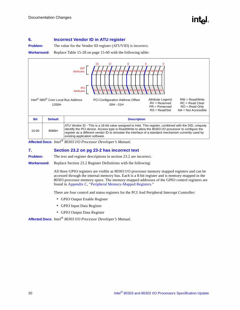
6. Incorrect Vendor ID in ATU registerProblem: The value for the Vendor ID register (ATUVID) is incorrect.
Workaround: Replace Table 15-28 on page 15-60 with the following table:
Affected Docs: Intel® 80303 I/O Processor Developer’s Manual.
7. Section 23.2 on pg 23-2 has incorrect textProblem: The text and register descriptions in section 23.2 are incorrect.
Workaround: Replace Section 23.2 Register Definitions with the following:
All three GPIO registers are visible as 80303 I/O processor memory mapped registers and can be accessed through the internal memory bus. Each is a 8-bit register and is memory-mapped in the 80303 processor memory space. The memory-mapped addresses of the GPIO control registers are found in Appendix C, “Peripheral Memory-Mapped Registers.”
There are four control and status registers for the PCI And Peripheral Interrupt Controller:
• GPIO Output Enable Register
• GPIO Input Data Register
• GPIO Output Data Register
Affected Docs: Intel® 80303 I/O Processor Developer’s Manual.
Bit Default Description
15:00 8086H
ATU Vendor ID - This is a 16-bit value assigned to Intel. This register, combined with the DID, uniquely identify the PCI device. Access type is Read/Write to allow the 80303 I/O processor to configure the register as a different vendor ID to simulate the interface of a standard mechanism currently used by existing application software.
PCI
IOPAttributes
Attributes
15 12 8 4 0
rw
ro
rw
ro
rw
ro
rw
ro
rw
ro
rw
ro
rw
ro
rw
ro
rw
ro
rw
ro
rw
ro
rw
ro
rw
ro
rw
ro
rw
ro
rw
ro
Attribute Legend:RV = ReservedPR = PreservedRS = Read/Set
RW = Read/WriteRC = Read ClearRO = Read Only
NA = Not Accessible
Intel® i960® Core Local Bus Address
1200H
PCI Configuration Address Offset
00H - 01H

Intel® 80303 and 80302 I/O Processors Specification Update 21
Documentation Changes
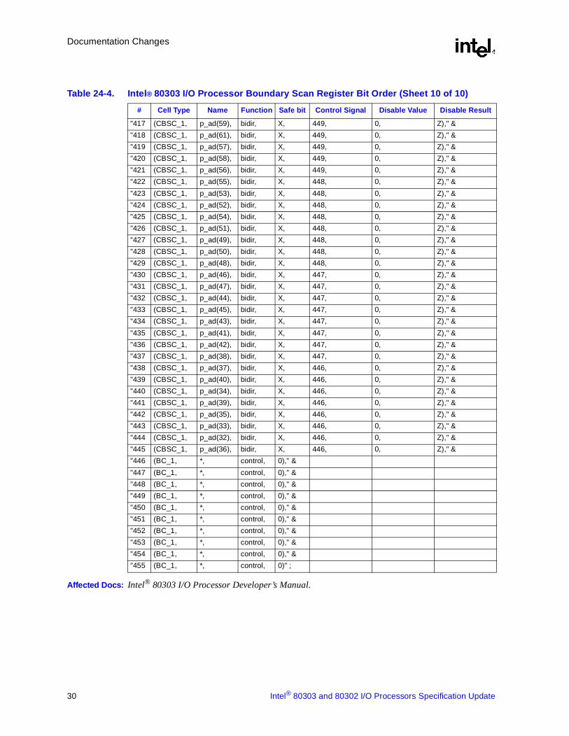
8. Table 24-4 on pg 24-8 is incorrectProblem: Table 24-4 on pg 24-8 is incorrect.
Workaround: Replace Table 24-4 with the following table:
Table 24-4. Intel® 80303 I/O Processor Boundary Scan Register Bit Order (Sheet 1 of 10)
# Cell Type Name Function Safe bit Control Signal Disable Value Disable Result
"0 (CBSC_1, scl, bidir, X, 1, 1, Z)," &
"1 (BC_1, *, control, 1)," &
"2 (CBSC_1, sda, bidir, X, 3, 1, Z)," &
"3 (BC_1, *, control, 1)," &
"4 (BC_1, rale, output3, X, 111, 1, Z)," &
"5 (BC_1, roez, output3, X, 111, 1, Z)," &
"6 (CBSC_1, rad(15), bidir, X, 7, 0, Z)," &
"7 (BC_1, *, control, 0)," &
"8 (BC_1, rcez(1), output3, X, 9, 0, Z)," &
"9 (BC_1, *, control, 0)," &
"10 (BC_1, rcez(0), output3, X, 11, 0, Z)," &
"11 (BC_1, *, control, 0)," &
"12 (CBSC_1, rad(6), bidir, X, 28, 1, Z)," &
"13 (BC_1, rwez, output3, X, 111, 1, Z)," &
"14 (CBSC_1, rad(9), bidir, X, 18, 0, Z)," &
"15 (CBSC_1, rad(10), bidir, X, 16, 0, Z)," &
"16 (BC_1, *, control, 0)," &
"17 (CBSC_1, rad(11), bidir, X, 18, 0, Z)," &
"18 (BC_1, *, control, 0)," &
"19 (CBSC_1, rad(13), bidir, X, 20, 0, Z)," &
"20 (BC_1, *, control, 0)," &
"21 (CBSC_1, rad(12), bidir, X, 22, 0, Z)," &
"22 (BC_1, *, control, 0)," &
"23 (CBSC_1, rad(8), bidir, X, 28, 1, Z)," &
"24 (CBSC_1, rad(14), bidir, X, 25, 0, Z)," &
"25 (BC_1, *, control, 0)," &
"26 (CBSC_1, rad(2), bidir, X, 28, 1, Z)," &
"27 (CBSC_1, rad(1), bidir, X, 28, 1, Z)," &
"28 (BC_1, *, control, 1)," &
"29 (CBSC_1, rad(16), bidir, X, 30, 0, Z)," &
"30 (BC_1, *, control, 0)," &
"31 (CBSC_1, rad(0), bidir, X, 28, 1, Z)," &
"32 (CBSC_1, rad(5), bidir, X, 28, 1, Z)," &
"33 (CBSC_1, rad(4), bidir, X, 28, 1, Z)," &
"34 (CBSC_1, rad(3), bidir, X, 28, 1, Z)," &
"35 (BC_4, nc1, input, X)," &
"36 (CBSC_1, rad(7), bidir, X, 28, 1, Z)," &
"37 (CBSC_1, GPIO(0), bidir, X, 38, 1, Z)," &
"38 (BC_1, *, control, 1)," &
"39 (CBSC_1, GPIO(1), bidir, X, 40, 1, Z)," &
"40 (BC_1, *, control, 1)," &
"41 (CBSC_1, GPIO(2), bidir, X, 42, 1, Z)," &

Documentation Changes
22 Intel® 80303 and 80302 I/O Processors Specification Update
"42 (BC_1, *, control, 1)," &
"43 (BC_1, i_rstz, output3, X, 111, 1, Z)," &
"44 (CBSC_1, GPIO(3), bidir, X, 45, 1, Z)," &
"45 (BC_1, *, control, 1)," &
"46 (CBSC_1, GPIO(4), bidir, X, 47, 1, Z)," &
"47 (BC_1, *, control, 1)," &
"48 (CBSC_1, GPIO(5), bidir, X, 49, 1, Z)," &
"49 (BC_1, *, control, 1)," &
"50 (CBSC_1, GPIO(6), bidir, X, 51, 1, Z)," &
"51 (BC_1, *, control, 1)," &
"52 (CBSC_1, GPIO(7), bidir, X, 53, 1, Z)," &
"53 (BC_1, *, control, 1)," &
"54 (BC_4, irqz(0), input, X)," &
"55 (BC_4, irqz(1), input, X)," &
"56 (BC_4, irqz(2), input, X)," &
"57 (BC_4, irqz(3), input, X)," &
"58 (BC_4, irqz(4), input, X)," &
"59 (BC_4, irqz(5), input, X)," &
"60 (BC_1, nc2, output3, X, 65, 1, Z)," &
"61 (BC_4, lcdinitz, input, X)," &
"62 (BC_4, logic1, input, X)," &
"63 (BC_1, failz, output3, X, 110, 1, Z)," &
"64 (BC_4, nmiz, input, X)," &
"65 (BC_1, *, control, 1)," &
"66 (BC_4, nc3, input, X)," &
"67 (BC_4, nc4, input, X)," &
"68 (BC_4, nc5, input, X)," &
"69 (BC_4, nc6, input, X)," &
"70 (BC_4, nc7, input, X)," &
"71 (BC_4, nc8, input, X)," &
"72 (BC_4, nc9, input, X)," &
"73 (BC_4, nc10, input, X)," &
"74 (BC_4, nc11, input, X)," &
"75 (BC_4, nc12, input, X)," &
"76 (BC_4, nc20, input, X)," &
"77 (BC_4, nc13, input, X)," &
"78 (BC_4, nc15, input, X)," &
"79 (BC_4, nc14, input, X)," &
"80 (BC_4, nc16, input, X)," &
"81 (BC_4, pwrdelay, input, X)," &
"82 (BC_1, nc17, output3, X, 65, 1, Z)," &
"83 (BC_1, nc19, output3, X, 65, 1, Z)," &
"84 (BC_1, nc18, output3, X, 85, 1, Z)," &
"85 (BC_1, *, control, 1)," &
"86 (BC_1, dclk(3), output3, X, 111, 1, Z)," &
"87 (BC_1, dclk(2), output3, X, 111, 1, Z)," &
"88 (BC_1, dclk(1), output3, X, 111, 1, Z)," &
Table 24-4. Intel® 80303 I/O Processor Boundary Scan Register Bit Order (Sheet 2 of 10)
# Cell Type Name Function Safe bit Control Signal Disable Value Disable Result

Intel® 80303 and 80302 I/O Processors Specification Update 23
Documentation Changes
"89 (BC_1, dclk(0), output3, X, 111, 1, Z)," &
"90 (BC_1, dclkout, output3, X, 111, 1, Z)," &
"91 (CBSC_1, dq(35), bidir, X, 95, 0, Z)," &
"92 (CBSC_1, dq(0), bidir, X, 93, 0, Z)," &
"93 (BC_1, *, control, 0)," &
"94 (CBSC_1, dq(32), bidir, X, 95, 0, Z)," &
"95 (BC_1, *, control, 0)," &
"96 (CBSC_1, dq(2), bidir, X, 93, 0, Z)," &
"97 (CBSC_1, dq(36), bidir, X, 95, 0, Z)," &
"98 (CBSC_1, dq(33), bidir, X, 95, 0, Z)," &
"99 (CBSC_1, dq(1), bidir, X, 93, 0, Z)," &
"100 (CBSC_1, dq(34), bidir, X, 95, 0, Z)," &
"101 (CBSC_1, dq(37), bidir, X, 95, 0, Z)," &
"102 (CBSC_1, dq(4), bidir, X, 93, 0, Z)," &
"103 (CBSC_1, dq(39), bidir, X, 95, 0, Z)," &
"104 (CBSC_1, dq(41), bidir, X, 95, 0, Z)," &
"105 (CBSC_1, dq(38), bidir, X, 95, 0, Z)," &
"106 (CBSC_1, dq(3), bidir, X, 93, 0, Z)," &
"107 (CBSC_1, dq(43), bidir, X, 108, 0, Z)," &
"108 (BC_1, *, control, 0)," &
"109 (CBSC_1, dq(40), bidir, X, 95, 0, Z)," &
"110 (BC_1, *, control, 1)," &
"111 (BC_1, *, control, 1)," &
"112 (CBSC_1, dq(5), bidir, X, 202, 0, Z)," &
"113 (CBSC_1, dq(6), bidir, X, 202, 0, Z)," &
"114 (CBSC_1, dq(8), bidir, X, 202, 0, Z)," &
"115 (CBSC_1, dq(42), bidir, X, 204, 0, Z)," &
"116 (CBSC_1, dq(7), bidir, X, 202, 0, Z)," &
"117 (CBSC_1, dq(45), bidir, X, 204, 0, Z)," &
"118 (CBSC_1, dq(44), bidir, X, 204, 0, Z)," &
"119 (CBSC_1, dq(9), bidir, X, 202, 0, Z)," &
"120 (CBSC_1, dq(47), bidir, X, 204, 0, Z)," &
"121 (CBSC_1, dq(12), bidir, X, 202, 0, Z)," &
"122 (CBSC_1, dq(10), bidir, X, 202, 0, Z)," &
"123 (CBSC_1, dq(11), bidir, X, 202, 0, Z)," &
"124 (CBSC_1, dq(46), bidir, X, 204, 0, Z)," &
"125 (CBSC_1, dq(14), bidir, X, 202, 0, Z)," &
"126 (CBSC_1, dq(13), bidir, X, 202, 0, Z)," &
"127 (CBSC_1, scb(5), bidir, X, 200, 0, Z)," &
"128 (CBSC_1, dq(15), bidir, X, 202, 0, Z)," &
"129 (CBSC_1, scb(4), bidir, X, 200, 0, Z)," &
"130 (BC_1, sdqm(4), output3, X, 205, 1, Z)," &
"131 (BC_1, scasz, output3, X, 205, 1, Z)," &
"132 (CBSC_1, scb(0), bidir, X, 200, 0, Z)," &
"133 (BC_1, swez, output3, X, 205, 1, Z)," &
"134 (CBSC_1, scb(1), bidir, X, 200, 0, Z)," &
"135 (BC_1, sdqm(0), output3, X, 205, 1, Z)," &
Table 24-4. Intel® 80303 I/O Processor Boundary Scan Register Bit Order (Sheet 3 of 10)
# Cell Type Name Function Safe bit Control Signal Disable Value Disable Result

Documentation Changes
24 Intel® 80303 and 80302 I/O Processors Specification Update
"136 (BC_1, scez(1), output3, X, 205, 1, Z)," &
"137 (BC_1, sdqm(5), output3, X, 205, 1, Z)," &
"138 (BC_1, sdqm(1), output3, X, 205, 1, Z)," &
"139 (BC_1, scez(0), output3, X, 205, 1, Z)," &
"140 (BC_1, sa(0), output3, X, 205, 1, Z)," &
"141 (BC_1, srasz, output3, X, 205, 1, Z)," &
"142 (BC_1, sa(1), output3, X, 205, 1, Z)," &
"143 (BC_1, sa(2), output3, X, 205, 1, Z)," &
"144 (BC_1, sa(4), output3, X, 205, 1, Z)," &
"145 (BC_1, sa(3), output3, X, 205, 1, Z)," &
"146 (BC_1, sa(5), output3, X, 205, 1, Z)," &
"147 (BC_1, sa(6), output3, X, 205, 1, Z)," &
"148 (BC_1, sa(8), output3, X, 205, 1, Z)," &
"149 (BC_1, sa(7), output3, X, 205, 1, Z)," &
"150 (BC_1, sa(9), output3, X, 205, 1, Z)," &
"151 (BC_1, sba(0), output3, X, 205, 1, Z)," &
"152 (BC_1, sa(11), output3, X, 205, 1, Z)," &
"153 (BC_1, sa(10), output3, X, 205, 1, Z)," &
"154 (BC_1, sba(1), output3, X, 205, 1, Z)," &
"155 (BC_4, dclkin, input, X)," &
"156 (BC_1, sa(12), output3, X, 205, 1, Z)," &
"157 (BC_1, sdqm(2), output3, X, 205, 1, Z)," &
"158 (BC_1, sdqm(3), output3, X, 205, 1, Z)," &
"159 (BC_1, scke(0), output3, X, 205, 1, Z)," &
"160 (BC_1, sdqm(6), output3, X, 205, 1, Z)," &
"161 (CBSC_1, scb(2), bidir, X, 200, 0, Z)," &
"162 (CBSC_1, scb(3), bidir, X, 200, 0, Z)," &
"163 (BC_1, sdqm(7), output3, X, 205, 1, Z)," &
"164 (BC_1, sa(13), output3, X, 205, 1, Z)," &
"165 (CBSC_1, scb(6), bidir, X, 200, 0, Z)," &
"166 (CBSC_1, dq(16), bidir, X, 201, 0, Z)," &
"167 (CBSC_1, dq(17), bidir, X, 201, 0, Z)," &
"168 (CBSC_1, scb(7), bidir, X, 200, 0, Z)," &
"169 (CBSC_1, dq(48), bidir, X, 204, 0, Z)," &
"170 (CBSC_1, dq(18), bidir, X, 201, 0, Z)," &
"171 (CBSC_1, dq(49), bidir, X, 204, 0, Z)," &
"172 (CBSC_1, dq(19), bidir, X, 201, 0, Z)," &
"173 (CBSC_1, dq(50), bidir, X, 204, 0, Z)," &
"174 (CBSC_1, dq(20), bidir, X, 201, 0, Z)," &
"175 (CBSC_1, dq(51), bidir, X, 204, 0, Z)," &
"176 (CBSC_1, dq(21), bidir, X, 201, 0, Z)," &
"177 (BC_1, scke(1), output3, X, 205, 1, Z)," &
"178 (CBSC_1, dq(22), bidir, X, 201, 0, Z)," &
"179 (CBSC_1, dq(52), bidir, X, 204, 0, Z)," &
"180 (CBSC_1, dq(23), bidir, X, 201, 0, Z)," &
"181 (CBSC_1, dq(53), bidir, X, 204, 0, Z)," &
"182 (CBSC_1, dq(24), bidir, X, 201, 0, Z)," &
Table 24-4. Intel® 80303 I/O Processor Boundary Scan Register Bit Order (Sheet 4 of 10)
# Cell Type Name Function Safe bit Control Signal Disable Value Disable Result

Intel® 80303 and 80302 I/O Processors Specification Update 25
Documentation Changes
"183 (CBSC_1, dq(54), bidir, X, 204, 0, Z)," &
"184 (CBSC_1, dq(55), bidir, X, 204, 0, Z)," &
"185 (CBSC_1, dq(25), bidir, X, 201, 0, Z)," &
"186 (CBSC_1, dq(26), bidir, X, 201, 0, Z)," &
"187 (CBSC_1, dq(56), bidir, X, 204, 0, Z)," &
"188 (CBSC_1, dq(27), bidir, X, 201, 0, Z)," &
"189 (CBSC_1, dq(57), bidir, X, 204, 0, Z)," &
"190 (CBSC_1, dq(28), bidir, X, 201, 0, Z)," &
"191 (CBSC_1, dq(59), bidir, X, 204, 0, Z)," &
"192 (CBSC_1, dq(58), bidir, X, 204, 0, Z)," &
"193 (CBSC_1, dq(30), bidir, X, 201, 0, Z)," &
"194 (CBSC_1, dq(29), bidir, X, 201, 0, Z)," &
"195 (CBSC_1, dq(60), bidir, X, 204, 0, Z)," &
"196 (CBSC_1, dq(61), bidir, X, 204, 0, Z)," &
"197 (CBSC_1, dq(31), bidir, X, 201, 0, Z)," &
"198 (CBSC_1, dq(62), bidir, X, 204, 0, Z)," &
"199 (CBSC_1, dq(63), bidir, X, 204, 0, Z)," &
"200 (BC_1, *, control, 0)," &
"201 (BC_1, *, control, 0)," &
"202 (BC_1, *, control, 0)," &
"203 (BC_1, *, control, 0)," &
"204 (BC_1, *, control, 0)," &
"205 (BC_1, *, control, 1)," &
"206 (CBSC_1, s_ad(38), bidir, X, 325, 0, Z)," &
"207 (CBSC_1, s_ad(34), bidir, X, 325, 0, Z)," &
"208 (CBSC_1, s_ad(42), bidir, X, 325, 0, Z)," &
"209 (CBSC_1, s_ad(36), bidir, X, 325, 0, Z)," &
"210 (CBSC_1, s_ad(33), bidir, X, 325, 0, Z)," &
"211 (CBSC_1, s_ad(32), bidir, X, 325, 0, Z)," &
"212 (CBSC_1, s_ad(40), bidir, X, 325, 0, Z)," &
"213 (CBSC_1, s_ad(37), bidir, X, 325, 0, Z)," &
"214 (CBSC_1, s_ad(46), bidir, X, 324, 0, Z)," &
"215 (CBSC_1, s_ad(35), bidir, X, 324, 0, Z)," &
"216 (CBSC_1, s_ad(44), bidir, X, 324, 0, Z)," &
"217 (CBSC_1, s_ad(39), bidir, X, 324, 0, Z)," &
"218 (CBSC_1, s_ad(41), bidir, X, 324, 0, Z)," &
"219 (CBSC_1, s_ad(50), bidir, X, 324, 0, Z)," &
"220 (CBSC_1, s_ad(48), bidir, X, 324, 0, Z)," &
"221 (CBSC_1, s_ad(45), bidir, X, 324, 0, Z)," &
"222 (CBSC_1, s_ad(47), bidir, X, 323, 0, Z)," &
"223 (CBSC_1, s_ad(54), bidir, X, 323, 0, Z)," &
"224 (CBSC_1, s_ad(43), bidir, X, 323, 0, Z)," &
"225 (CBSC_1, s_ad(49), bidir, X, 323, 0, Z)," &
"226 (CBSC_1, s_ad(52), bidir, X, 323, 0, Z)," &
"227 (CBSC_1, s_ad(53), bidir, X, 323, 0, Z)," &
"228 (CBSC_1, s_ad(51), bidir, X, 323, 0, Z)," &
"229 (CBSC_1, s_ad(58), bidir, X, 323, 0, Z)," &
Table 24-4. Intel® 80303 I/O Processor Boundary Scan Register Bit Order (Sheet 5 of 10)
# Cell Type Name Function Safe bit Control Signal Disable Value Disable Result

Documentation Changes
26 Intel® 80303 and 80302 I/O Processors Specification Update
"230 (CBSC_1, s_ad(56), bidir, X, 322, 0, Z)," &
"231 (CBSC_1, s_ad(57), bidir, X, 322, 0, Z)," &
"232 (CBSC_1, s_ad(55), bidir, X, 322, 0, Z)," &
"233 (CBSC_1, s_ad(60), bidir, X, 322, 0, Z)," &
"234 (CBSC_1, s_ad(59), bidir, X, 322, 0, Z)," &
"235 (CBSC_1, s_ad(62), bidir, X, 322, 0, Z)," &
"236 (CBSC_1, s_ad(61), bidir, X, 322, 0, Z)," &
"237 (CBSC_1, s_cbez(5), bidir, X, 331, 0, Z)," &
"238 (CBSC_1, s_par64, bidir, X, 239, 0, Z)," &
"239 (BC_1, *, control, 0)," &
"240 (CBSC_1, s_cbez(4), bidir, X, 331, 0, Z)," &
"241 (CBSC_1, s_req64z, bidir, X, 242, 0, Z)," &
"242 (BC_1, *, control, 0)," &
"243 (CBSC_1, s_ad(63), bidir, X, 322, 0, Z)," &
"244 (CBSC_1, s_cbez(7), bidir, X, 331, 0, Z)," &
"245 (CBSC_1, s_ack64z, bidir, X, 246, 0, Z)," &
"246 (BC_1, *, control, 0)," &
"247 (CBSC_1, s_ad(0), bidir, X, 329, 0, Z)," &
"248 (CBSC_1, s_ad(2), bidir, X, 329, 0, Z)," &
"249 (CBSC_1, s_cbez(6), bidir, X, 331, 0, Z)," &
"250 (CBSC_1, s_ad(8), bidir, X, 328, 0, Z)," &
"251 (CBSC_1, s_ad(3), bidir, X, 329, 0, Z)," &
"252 (CBSC_1, s_ad(4), bidir, X, 329, 0, Z)," &
"253 (CBSC_1, s_ad(7), bidir, X, 329, 0, Z)," &
"254 (CBSC_1, s_ad(1), bidir, X, 329, 0, Z)," &
"255 (CBSC_1, s_cbez(0), bidir, X, 330, 0, Z)," &
"256 (CBSC_1, s_ad(5), bidir, X, 329, 0, Z)," &
"257 (CBSC_1, s_ad(6), bidir, X, 328, 0, Z)," &
"258 (CBSC_1, s_ad(10), bidir, X, 328, 0, Z)," &
"259 (BC_4, s_m66en, input, X)," &
"260 (CBSC_1, s_ad(12), bidir, X, 328, 0, Z)," &
"261 (CBSC_1, s_ad(11), bidir, X, 328, 0, Z)," &
"262 (CBSC_1, s_ad(9), bidir, X, 329, 0, Z)," &
"263 (CBSC_1, s_ad(14), bidir, X, 328, 0, Z)," &
"264 (CBSC_1, s_serrz, bidir, X, 265, 0, Z)," &
"265 (BC_1, *, control, 0)," &
"266 (CBSC_1, s_ad(15), bidir, X, 328, 0, Z)," &
"267 (CBSC_1, s_cbez(1), bidir, X, 330, 0, Z)," &
"268 (CBSC_1, s_ad(13), bidir, X, 328, 0, Z)," &
"269 (CBSC_1, s_par, bidir, X, 270, 0, Z)," &
"270 (BC_1, *, control, 0)," &
"271 (CBSC_1, s_stopz, bidir, X, 280, 0, Z)," &
"272 (CBSC_1, s_perrz, bidir, X, 273, 0, Z)," &
"273 (BC_1, *, control, 0)," &
"274 (CBSC_1, s_lockz, bidir, X, 275, 0, Z)," &
"275 (BC_1, *, control, 0)," &
"276 (CBSC_1, s_trdyz, bidir, X, 280, 0, Z)," &
Table 24-4. Intel® 80303 I/O Processor Boundary Scan Register Bit Order (Sheet 6 of 10)
# Cell Type Name Function Safe bit Control Signal Disable Value Disable Result

Intel® 80303 and 80302 I/O Processors Specification Update 27
Documentation Changes
"277 (CBSC_1, s_framez, bidir, X, 278, 0, Z)," &
"278 (BC_1, *, control, 0)," &
"279 (CBSC_1, s_devselz, bidir, X, 280, 0, Z)," &
"280 (BC_1, *, control, 0)," &
"281 (CBSC_1, s_irdyz, bidir, X, 282, 0, Z)," &
"282 (BC_1, *, control, 0)," &
"283 (CBSC_1, s_ad(16), bidir, X, 327, 0, Z)," &
"284 (CBSC_1, s_ad(18), bidir, X, 327, 0, Z)," &
"285 (CBSC_1, s_cbez(2), bidir, X, 330, 0, Z)," &
"286 (CBSC_1, s_ad(17), bidir, X, 327, 0, Z)," &
"287 (CBSC_1, s_ad(20), bidir, X, 327, 0, Z)," &
"288 (CBSC_1, s_ad(21), bidir, X, 327, 0, Z)," &
"289 (CBSC_1, s_ad(19), bidir, X, 327, 0, Z)," &
"290 (CBSC_1, s_ad(24), bidir, X, 327, 0, Z)," &
"291 (CBSC_1, s_ad(22), bidir, X, 327, 0, Z)," &
"292 (CBSC_1, s_ad(26), bidir, X, 326, 0, Z)," &
"293 (CBSC_1, s_ad(23), bidir, X, 326, 0, Z)," &
"294 (CBSC_1, s_cbez(3), bidir, X, 330, 0, Z)," &
"295 (CBSC_1, s_ad(28), bidir, X, 326, 0, Z)," &
"296 (CBSC_1, s_ad(25), bidir, X, 326, 0, Z)," &
"297 (CBSC_1, s_ad(30), bidir, X, 326, 0, Z)," &
"298 (CBSC_1, s_ad(27), bidir, X, 326, 0, Z)," &
"299 (CBSC_1, s_ad(29), bidir, X, 326, 0, Z)," &
"300 (CBSC_1, s_ad(31), bidir, X, 326, 0, Z)," &
"301 (BC_1, s_rstz, output3, X, 333, 1, Z)," &
"302 (BC_1, s_holdaz, output3, X, 321, 0, Z)," &
"303 (BC_4, s_holdz, input, X)," &
"304 (BC_1, s_gntz(0), output3, X, 321, 0, Z)," &
"305 (BC_1, s_clk(0), output3, X, 333, 1, Z)," &
"306 (BC_1, s_clk(1), output3, X, 333, 1, Z)," &
"307 (BC_1, s_clk(2), output3, X, 333, 1, Z)," &
"308 (BC_1, s_clk(3), output3, X, 333, 1, Z)," &
"309 (BC_1, s_clk(4), output3, X, 333, 1, Z)," &
"310 (BC_1, s_clk(5), output3, X, 333, 1, Z)," &
"311 (BC_1, r_clkout, output3, X, 332, 1, Z)," &
"312 (BC_4, r_clkin, input, X)," &
"313 (BC_4, s_reqz(0), input, X)," &
"314 (BC_4, s_reqz(1), input, X)," &
"315 (BC_4, s_reqz(2), input, X)," &
"316 (BC_1, s_gntz(1), output3, X, 321, 0, Z)," &
"317 (BC_1, s_gntz(2), output3, X, 321, 0, Z)," &
"318 (BC_4, s_reqz(3), input, X)," &
"319 (BC_1, s_gntz(3), output3, X, 321, 0, Z)," &
"320 (BC_4, s_reqz(4), input, X)," &
"321 (BC_1, *, control, 0)," &
"322 (BC_1, *, control, 0)," &
"323 (BC_1, *, control, 0)," &
Table 24-4. Intel® 80303 I/O Processor Boundary Scan Register Bit Order (Sheet 7 of 10)
# Cell Type Name Function Safe bit Control Signal Disable Value Disable Result

Documentation Changes
28 Intel® 80303 and 80302 I/O Processors Specification Update
"324 (BC_1, *, control, 0)," &
"325 (BC_1, *, control, 0)," &
"326 (BC_1, *, control, 0)," &
"327 (BC_1, *, control, 0)," &
"328 (BC_1, *, control, 0)," &
"329 (BC_1, *, control, 0)," &
"330 (BC_1, *, control, 0)," &
"331 (BC_1, *, control, 0)," &
"332 (BC_1, *, control, 1)," &
"333 (BC_1, *, control, 1)," &
"334 (BC_1, s_gntz(4), output3, X, 337, 0, Z)," &
"335 (BC_4, s_reqz(5), input, X)," &
"336 (BC_1, s_gntz(5), output3, X, 337, 0, Z)," &
"337 (BC_1, *, control, 0)," &
"338 (BC_1, p_intz(1), output3, X, 339, 0, Z)," &
"339 (BC_1, *, control, 0)," &
"340 (BC_4, p_gntz, input, X)," &
"341 (CBSC_1, p_ad(28), bidir, X, 455, 0, Z)," &
"342 (BC_4, p_rstz, input, X)," &
"343 (BC_1, p_intz(3), output3, X, 344, 0, Z)," &
"344 (BC_1, *, control, 0)," &
"345 (CBSC_1, p_ad(30), bidir, X, 455, 0, Z)," &
"346 (BC_1, p_intz(2), output3, X, 347, 0, Z)," &
"347 (BC_1, *, control, 0)," &
"348 (BC_1, p_intz(0), output3, X, 349, 0, Z)," &
"349 (BC_1, *, control, 0)," &
"350 (CBSC_1, p_ad(31), bidir, X, 455, 0, Z)," &
"351 (BC_1, p_reqz, output3, X, 352, 0, Z)," &
"352 (BC_1, *, control, 0)," &
"353 (CBSC_1, p_ad(26), bidir, X, 455, 0, Z)," &
"354 (CBSC_1, p_ad(29), bidir, X, 455, 0, Z)," &
"355 (CBSC_1, p_ad(22), bidir, X, 454, 0, Z)," &
"356 (BC_4, p_idsel, input, X)," &
"357 (CBSC_1, p_ad(25), bidir, X, 455, 0, Z)," &
"358 (CBSC_1, p_ad(24), bidir, X, 455, 0, Z)," &
"359 (CBSC_1, p_ad(27), bidir, X, 455, 0, Z)," &
"360 (CBSC_1, p_ad(20), bidir, X, 454, 0, Z)," &
"361 (CBSC_1, p_ad(23), bidir, X, 454, 0, Z)," &
"362 (CBSC_1, p_cbez(3), bidir, X, 453, 0, Z)," &
"363 (CBSC_1, p_ad(21), bidir, X, 454, 0, Z)," &
"364 (CBSC_1, p_ad(18), bidir, X, 454, 0, Z)," &
"365 (CBSC_1, p_ad(19), bidir, X, 454, 0, Z)," &
"366 (CBSC_1, p_ad(16), bidir, X, 454, 0, Z)," &
"367 (CBSC_1, p_ad(17), bidir, X, 454, 0, Z)," &
"368 (CBSC_1, p_framez, bidir, X, 369, 0, Z)," &
"369 (BC_1, *, control, 0)," &
"370 (CBSC_1, p_cbez(2), bidir, X, 453, 0, Z)," &
Table 24-4. Intel® 80303 I/O Processor Boundary Scan Register Bit Order (Sheet 8 of 10)
# Cell Type Name Function Safe bit Control Signal Disable Value Disable Result

Intel® 80303 and 80302 I/O Processors Specification Update 29
Documentation Changes
"371 (CBSC_1, p_stopz, bidir, X, 373, 0, Z)," &
"372 (CBSC_1, p_trdyz, bidir, X, 373, 0, Z)," &
"373 (BC_1, *, control, 0)," &
"374 (CBSC_1, p_devselz, bidir, X, 373, 0, Z)," &
"375 (CBSC_1, p_irdyz, bidir, X, 376, 0, Z)," &
"376 (BC_1, *, control, 0)," &
"377 (CBSC_1, p_ad(15), bidir, X, 452, 0, Z)," &
"378 (CBSC_1, p_par, bidir, X, 379, 0, Z)," &
"379 (BC_1, *, control, 0)," &
"380 (CBSC_1, p_perrz, bidir, X, 381, 0, Z)," &
"381 (BC_1, *, control, 0)," &
"382 (BC_4, p_lockz, input, X)," &
"383 (CBSC_1, p_ad(11), bidir, X, 452, 0, Z)," &
"384 (CBSC_1, p_ad(13), bidir, X, 452, 0, Z)," &
"385 (CBSC_1, p_cbez(1), bidir, X, 453, 0, Z)," &
"386 (CBSC_1, p_serrz, bidir, X, 387, 0, Z)," &
"387 (BC_1, *, control, 0)," &
"388 (CBSC_1, p_cbez(0), bidir, X, 453, 0, Z)," &
"389 (CBSC_1, p_ad(9), bidir, X, 452, 0, Z)," &
"390 (CBSC_1, p_ad(12), bidir, X, 452, 0, Z)," &
"391 (CBSC_1, p_ad(14), bidir, X, 452, 0, Z)," &
"392 (CBSC_1, p_ad(10), bidir, X, 452, 0, Z)," &
"393 (BC_4, p_m66en, input, X)," &
"394 (CBSC_1, p_ad(6), bidir, X, 452, 0, Z)," &
"395 (CBSC_1, p_ad(4), bidir, X, 451, 0, Z)," &
"396 (CBSC_1, p_ad(8), bidir, X, 451, 0, Z)," &
"397 (CBSC_1, p_ad(7), bidir, X, 451, 0, Z)," &
"398 (BC_4, p_clk, input, X)," &
"399 (CBSC_1, p_ad(2), bidir, X, 451, 0, Z)," &
"400 (CBSC_1, p_ad(5), bidir, X, 451, 0, Z)," &
"401 (CBSC_1, p_ad(3), bidir, X, 451, 0, Z)," &
"402 (CBSC_1, p_ad(0), bidir, X, 451, 0, Z)," &
"403 (CBSC_1, p_req64z, bidir, X, 404, 0, Z)," &
"404 (BC_1, *, control, 0)," &
"405 (CBSC_1, p_ad(1), bidir, X, 451, 0, Z)," &
"406 (CBSC_1, p_ack64z, bidir, X, 407, 0, Z)," &
"407 (BC_1, *, control, 0)," &
"408 (CBSC_1, p_cbez(7), bidir, X, 450, 0, Z)," &
"409 (CBSC_1, p_cbez(5), bidir, X, 450, 0, Z)," &
"410 (CBSC_1, p_cbez(6), bidir, X, 450, 0, Z)," &
"411 (CBSC_1, p_par64, bidir, X, 412, 0, Z)," &
"412 (BC_1, *, control, 0)," &
"413 (CBSC_1, p_cbez(4), bidir, X, 450, 0, Z)," &
"414 (CBSC_1, p_ad(62), bidir, X, 449, 0, Z)," &
"415 (CBSC_1, p_ad(63), bidir, X, 449, 0, Z)," &
"416 (CBSC_1, p_ad(60), bidir, X, 449, 0, Z)," &
Table 24-4. Intel® 80303 I/O Processor Boundary Scan Register Bit Order (Sheet 9 of 10)
# Cell Type Name Function Safe bit Control Signal Disable Value Disable Result
Documentation Changes
30 Intel® 80303 and 80302 I/O Processors Specification Update
Affected Docs: Intel® 80303 I/O Processor Developer’s Manual.
"417 (CBSC_1, p_ad(59), bidir, X, 449, 0, Z)," &
"418 (CBSC_1, p_ad(61), bidir, X, 449, 0, Z)," &
"419 (CBSC_1, p_ad(57), bidir, X, 449, 0, Z)," &
"420 (CBSC_1, p_ad(58), bidir, X, 449, 0, Z)," &
"421 (CBSC_1, p_ad(56), bidir, X, 449, 0, Z)," &
"422 (CBSC_1, p_ad(55), bidir, X, 448, 0, Z)," &
"423 (CBSC_1, p_ad(53), bidir, X, 448, 0, Z)," &
"424 (CBSC_1, p_ad(52), bidir, X, 448, 0, Z)," &
"425 (CBSC_1, p_ad(54), bidir, X, 448, 0, Z)," &
"426 (CBSC_1, p_ad(51), bidir, X, 448, 0, Z)," &
"427 (CBSC_1, p_ad(49), bidir, X, 448, 0, Z)," &
"428 (CBSC_1, p_ad(50), bidir, X, 448, 0, Z)," &
"429 (CBSC_1, p_ad(48), bidir, X, 448, 0, Z)," &
"430 (CBSC_1, p_ad(46), bidir, X, 447, 0, Z)," &
"431 (CBSC_1, p_ad(47), bidir, X, 447, 0, Z)," &
"432 (CBSC_1, p_ad(44), bidir, X, 447, 0, Z)," &
"433 (CBSC_1, p_ad(45), bidir, X, 447, 0, Z)," &
"434 (CBSC_1, p_ad(43), bidir, X, 447, 0, Z)," &
"435 (CBSC_1, p_ad(41), bidir, X, 447, 0, Z)," &
"436 (CBSC_1, p_ad(42), bidir, X, 447, 0, Z)," &
"437 (CBSC_1, p_ad(38), bidir, X, 447, 0, Z)," &
"438 (CBSC_1, p_ad(37), bidir, X, 446, 0, Z)," &
"439 (CBSC_1, p_ad(40), bidir, X, 446, 0, Z)," &
"440 (CBSC_1, p_ad(34), bidir, X, 446, 0, Z)," &
"441 (CBSC_1, p_ad(39), bidir, X, 446, 0, Z)," &
"442 (CBSC_1, p_ad(35), bidir, X, 446, 0, Z)," &
"443 (CBSC_1, p_ad(33), bidir, X, 446, 0, Z)," &
"444 (CBSC_1, p_ad(32), bidir, X, 446, 0, Z)," &
"445 (CBSC_1, p_ad(36), bidir, X, 446, 0, Z)," &
"446 (BC_1, *, control, 0)," &
"447 (BC_1, *, control, 0)," &
"448 (BC_1, *, control, 0)," &
"449 (BC_1, *, control, 0)," &
"450 (BC_1, *, control, 0)," &
"451 (BC_1, *, control, 0)," &
"452 (BC_1, *, control, 0)," &
"453 (BC_1, *, control, 0)," &
"454 (BC_1, *, control, 0)," &
"455 (BC_1, *, control, 0)" ;
Table 24-4. Intel® 80303 I/O Processor Boundary Scan Register Bit Order (Sheet 10 of 10)
# Cell Type Name Function Safe bit Control Signal Disable Value Disable Result

Intel® 80303 and 80302 I/O Processors Specification Update 31
Documentation Changes
9. Figure 25-1 on pg 25-1 has incorrect dataProblem: The Internal bus in diagram shows 66 MHz bus speed. The actual bus speed is 100 MHz
Workaround: Replace Figure 25-1 with the following:
Affected Docs: Intel® 80303 I/O Processor Developer’s Manual
10. Section 25.1.3 on page 25-2Problem: The third sentence of the first paragraph is incorrect. It states the maximum bus speed of the region
is 66 MHz. It is actually 100 MHz.
Workaround: Change the third sentence to the following:
“It supports clock frequencies up to a maximum of 100 MHz.”
Affected Docs: Intel® 80303 I/O Processor Developer’s Manual
Figure 25-1. Intel® 80303 I/O Processor Clocking Regions Diagram
A8053-01
P_CLK
R_CLKOUT
R_CLKIN
S_CLKOUT[5:0]
Intel® i960® JN CPU 100 MHz16K I-Cache4K D-Cache
Clock Region 3
Clock Region 1
Clock Region 2
Clock Region 4
ApplicationAccelerator
800 MBs Internal Bus (100MHz/64-bit)
64-B
it I/F
I2C
Bus
PerformanceMonitoring
Unit
MemoryController
I2CUnit
DC
LKO
UT
DC
LK[3
:0]
SC
L
DC
LKIN
Bus Interface Unit
6 Reg/Gnt Pairs
Primary PCI Bus
2 ChannelDMA
Controller
PrimaryAddress
TranslationUnit
PCI - to - PCIBridge
I20Messaging
Unit
Secondary PCI Bus
SecondaryAddress
TranslationUnit
1 ChannelDMA
Controller
SecondaryPCI Arbiter

Documentation Changes
32 Intel® 80303 and 80302 I/O Processors Specification Update
11. Figure 25-2 on pg 25-2 did not print correctlyProblem: Figure 25-2 on pg 25-2 did not print correctly.
Workaround: Replace Figure 25-2 with the following:
Affected Docs: Intel® 80303 I/O Processor Developer’s Manual.
12. Table 25-2 on page 25-3 did not print completelyProblem: Table 25-2 on page 25-3 did not print completely
Workaround: Replace Table 25-2 with the following:
Affected Docs: Intel® 80303 I/O Processor Developer’s Manual
Input Clock Region/Clock Buffered/PLL P_M66EN S_M66EN
P_CLK = 33 MHz
Region 1: 1x P_CLK Buffered
0 0Region 2: 3x P_CLK PLL
Region 3: 3x P_CLK PLL
Region 4: 1x P_CLK Buffered
P_CLK = 66 MHz
Region 1: 1x P_CLK Buffered
1 1Region 2: 3/2x P_CLK PLL
Region 3: 3/2x P_CLK PLL
Region 4: 1x P_CLK Buffered
P_CLK = 66 MHz
Region 1: 1x P_CLK Buffered
1 0Region 2: 3/2x P_CLK PLL
Region 3: 3/2x P_CLK PLL
Region 4: 1/2x P_CLK Buffered
NOTE: Combination of P_M66EN=0 and S_M66EN=1 is not supported by the Intel® 80303 I/O processor. When P_M66EN=0, the 80303 I/O processor forces S_M66EN=0 ensuring the unsupported condition never occurs.
A4662-02
SDRAMDIMM0
DQ(71:0)
I_CLK
P_CLK
DCLKin
DQ(71:0)
DCLKout
SDQ(71:0) SDQ(71:0)
CLK(3:0) CLK(3:0)
SDRAMDIMM1
Intel® 80303 and 80302 I/O Processors Specification Update 33
Documentation Changes
13. Section 1.2.2 on page 1-2 has incorrect dataProblem: The second sentence of the first paragraph is incorrect. It states the Internal Bus operates at
66 MHz. It is actually 100 MHz.
Workaround: Change the second sentence to the following:
“The Internal Bus operates at 100 MHz and is 64 bits wide.”
Affected Docs: Intel® 80303 I/O Processor Developer’s Manual
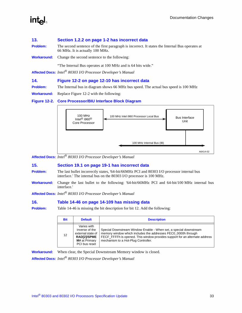
14. Figure 12-2 on page 12-10 has incorrect dataProblem: The Internal bus in diagram shows 66 MHz bus speed. The actual bus speed is 100 MHz
Workaround: Replace Figure 12-2 with the following:
Affected Docs: Intel® 80303 I/O Processor Developer’s Manual
15. Section 19.1 on page 19-1 has incorrect dataProblem: The last bullet incorrectly states, '64-bit/66MHz PCI and 80303 I/O processor internal bus
interface.' The internal bus on the 80303 I/O processor is 100 MHz.
Workaround: Change the last bullet to the following: '64-bit/66MHz PCI and 64-bit/100 MHz internal businterface.'
Affected Docs: Intel® 80303 I/O Processor Developer’s Manual
16. Table 14-46 on page 14-109 has missing dataProblem: Table 14-46 is missing the bit description for bit 12. Add the following:
Workaround: When clear, the Special Downstream Memory window is closed.
Affected Docs: Intel® 80303 I/O Processor Developer’s Manual
Figure 12-2. Core Processor/BIU Interface Block Diagram
Bit Default Description
12
Varies with inverse of the
external state of RAD[2]/SPMEM# at Primary PCI bus reset
Special Downstream Window Enable - When set, a special downstream memory window which includes the addresses FEC0_0000h through FECF_FFFFh is opened. This window provides support for an alternate address mechanism to a Hot-Plug Controller.
A6414-02
100 MHz Intel i960 Processor Local Bus100 MHzIntel® i960®
Core Processor
Bus InterfaceUnit
100 MHz Internal Bus (IB)
Documentation Changes
34 Intel® 80303 and 80302 I/O Processors Specification Update
17. Section 13.2.4.3 on page 13-30 has incorrect dataProblem: The first sentence incorrectly states, 'If enabled'. ECC is always enabled on the 80303 I/O
processor, it is not optional.
Workaround: Remove 'If enabled'.
Affected Docs: Intel® 80303 I/O Processor Developer’s Manual
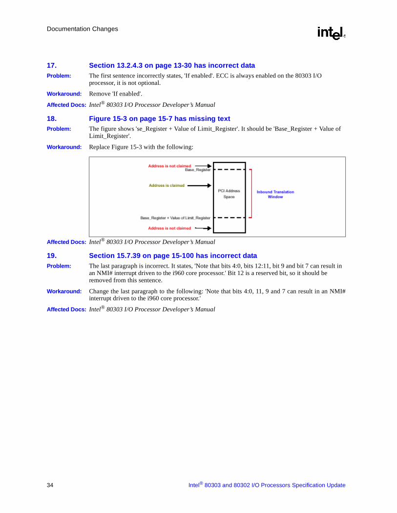
18. Figure 15-3 on page 15-7 has missing textProblem: The figure shows 'se_Register + Value of Limit_Register'. It should be 'Base_Register + Value of
Limit_Register'.
Workaround: Replace Figure 15-3 with the following:
Affected Docs: Intel® 80303 I/O Processor Developer’s Manual
19. Section 15.7.39 on page 15-100 has incorrect dataProblem: The last paragraph is incorrect. It states, 'Note that bits 4:0, bits 12:11, bit 9 and bit 7 can result in
an NMI# interrupt driven to the i960 core processor.' Bit 12 is a reserved bit, so it should be removed from this sentence.
Workaround: Change the last paragraph to the following: 'Note that bits 4:0, 11, 9 and 7 can result in an NMI#interrupt driven to the i960 core processor.'
Affected Docs: Intel® 80303 I/O Processor Developer’s Manual

Intel® 80303 and 80302 I/O Processors Specification Update 35
Documentation Changes
20. Table 8-17 on page 8-38 has incorrect dataProblem: The bit locations for External Interrupt 5 are incorrectly shown as bits '9:4'. It should be '7:4'.
Workaround: Replace Table 8-17 with the following:
Affected Docs: Intel® 80303 I/O Processor Developer’s Manual
21. Section 11.2.8 on page 11-5 has incorrect dataProblem: The last sentence in the third paragraph states, 'Specifications for a cold and warm reset can be
found in the 80960RM I/O Processor Data Sheet and the 80960RN I/O Processor Data Sheet.' This sentence should be removed, it does not pertain to the 80303 I/O processor.
Workaround: Change text to the following: 'The 80303 I/O processor complies with the PCI Local BusSpecification, Revision 2.2. Reset parameters are defined in this specification.'
Affected Docs: Intel® 80303 I/O Processor Developer’s Manual
22. Section 13.2.3.1 on page 13-13 has incorrect dataProblem: The first sentence states, 'The MCU supports an ECC only memory subsystem ranging from 32 to
528 Mbytes.' It should be 512 Mbytes, not 528 Mbytes.
Workaround: Change this sentence to the following: 'The MCU supports an ECC only memory subsystemranging from 32 to 512 Mbytes.'
Affected Docs: Intel® 80303 I/O Processor Developer’s Manual
23. Table 13-4 on page 13-9 has incorrect dataProblem: Table 13-4 lists incorrect wait states for the flash bus.
Workaround: Replace Table 13-4 with the following:
Affected Docs: Intel® 80303 I/O Processor Developer’s Manual
Bit Default Description
31:16Default
Value loaded from image in Control
Table
Reserved (initialize to 0)
15:12 External Interrupt 7 Field - IMAP1.x7
11:8 External Interrupt 6 Field - IMAP1.x6
7:4 External Interrupt 5 Field - IMAP1.x5
3:0 External Interrupt 4 Field - IMAP1.x4
Flash Speed Address-to-Data Wait States Recovery Wait States
<= 55 ns 8 4
<= 115 ns 12 4
<= 175 ns 20 4
PCI
IOPAttributes
Attributes
28 24 20 16 12 8 4 031
rv
na
rv
na
rv
na
rv
na
rv
na
rv
na
rv
na
rv
na
rv
na
rv
na
rv
na
rv
na
rv
na
rv
na
rv
na
rv
na
rw
na
rw
na
rw
na
rw
na
rw
na
rw
na
rw
na
rw
na
rw
na
rw
na
rw
na
rw
na
rw
na
rw
na
rw
na
rw
na
Attribute Legend:RV = ReservedPR = PreservedRS = Read/Set
RW = Read/WriteRC = Read ClearRO = Read OnlyNA= Not Accessible
IMAP1
Intel® i960® Core internal bus address
FF00 8524H

Documentation Changes
36 Intel® 80303 and 80302 I/O Processors Specification Update
24. Table 8-15 on page 8-36 needs clarificationProblem: ICON.10, Global Interrupt Enable bit, does not state what bit value enables interrupts.
Workaround: Add this sentence to the bit description, 'A '0' will globally enable interrupts, and a '1' globallydisables interrupts.'
Affected Docs: Intel® 80303 I/O Processor Developer’s Manual
25. Table 13-13 on page 13-30 has incorrect dataProblem: Syndrome Decoding Error Types and Symptoms are incorrectly stated.
Workaround: Replace Table 13-13 with the following and, add the adjacent paragraph with “new” Figure 13-16:
Figure 13-16 shows how the data flows through the ECC hardware for a read transaction.
Affected Docs: Intel® 80303 I/O Processor Developer’s Manual
Table 13-13. Syndrome Decoding
Error Type Symptom
None The syndrome is 0000 0000.
Single-Bit Use the H-Matrix in Figure 13-17 to determine which bit the MCU will invert to fix the error.
Multi-Bit If the Syndrome does not match an 8-bit value in the H-matrix, the error is uncorrectable
Figure 13-16. ECC Read Data Flow
A8160-01
MainMemory
MCU
ECCMemory
64-b
it B
us
Add
ress
and
Con
trol
Bus
8-bi
t Bus
64-b
it B
us
Error Type/Location
Calculate ECCwith G-matrix
H-matrixLook-up Table
Data to Internal Bus
Data Corrector(single-bit error)
Calculate Syndrome byComparing ECC w/Check Bits

Intel® 80303 and 80302 I/O Processors Specification Update 37
Documentation Changes
26. Section 13.2.4.3, First Paragraph after Table 13-13 has Incorrect DataProblem: First sentence incorrectly states error types for corrected Table 13-13:
...If decoding the syndrome indicates a double-bit or nibble error...
Should read as follows:...”When” decoding the syndrome indicates a “multi”-bit error...
Affected Docs: Intel® 80303 I/O Processor Developer’s Manual
27. Section 13.2.4.3, First Paragraph after “Current” Figure 13-16. H-Matrix has Incorrect Data
Problem: First sentence incorrectly states error types for corrected Table 13-13:...If error reporting is enabled in the ECCR and the MCU detects a nibble, single-bit, or double-bit error...
Should read as follows:...”When” error reporting is enabled in the ECCR and the MCU detects a single-bit or “multi”-bit error...
Affected Docs: Intel® 80303 I/O Processor Developer’s Manual
28. Section 11.3.1.5 FAIL# CodeProblem: The verbiage in this section is residual from the Intel® i960® I/O Processor Developer’s Manual,
where the internal bus was accessible from the outside. The internal bus is not accessible from the outside for i960 RM/RN I/O processor. Since the customer cannot “see” the internal bus, whatever is on it is not useful and is only confusing. Therefore, this section has been removed.
Affected Docs: Intel® 80303 I/O Processor Developer’s Manual
29. Section 13.5 Reset Conditions has Incorrect DataProblem: The last sentence in the first paragraph incorrectly states:
Reads issued prior to a write to the same address results in an ECC error (if enabled) and is not recommended.
This should state:Reads issued prior to a write to the same address results in an ECC error and are not recommended.
30. Section 13.2.4.2, First Sentence has Incorrect DataProblem: On page 13-28, the first sentence reads: “If the internal bus master writes less than the data bus
width programmed in the SDCR, then the MCU translates the write transaction into a read-modify-write transaction.” Please remove “programmed in the SDCR” from the sentence.
Affected Docs: Intel® 80303 I/O Processor Developer’s Manual
31. Section 13.6.2, Second Sentence has Incorrect Data
On page 13-46, the second sentence reads: “The SDCR specifies the drive strength for the MCU pins, the bus width, and power failure handling.” Please “remove, the bus width, and power failure handling” from the sentence. It should read “The SDCR specifies the drive strength for the MCU pins.”
Affected Docs: Intel® 80303 I/O Processor Developer’s Manual

Documentation Changes
38 Intel® 80303 and 80302 I/O Processors Specification Update
32. Section 4.5.2 on page 50 is only correct for A-0 and A-1 steppingsProblem: The second sentence in Note 7 states, ‘S_REQ64# is deasserted one P_CLK after the deassertion of
S_RST#’. This statement is not correct for the A-2 stepping of the 80303 and 80302 I/O processors.
Workaround: This statement is only correct for the A-0 and A-1 steppings of the 80303. See SpecificationClarification #6 for A-2 stepping functionality.
Affected Docs: Intel® 80303 I/O Processor Datasheet
33. Section 17.5.1 on page 17-12 is only correct for A-0 and A-1 steppingsProblem: The last sentence states, ‘S_REQ64# remains valid for one clock (P_CLK) after S_RST#
deasserts’. This statement is not correct for the A-2 stepping of the 80303 and 80302 I/O processors.
Workaround: This statement is only correct for the A-0 and A-1 steppings of the 80303. See SpecificationClarification #6 for A-2 stepping functionality.
Affected Docs: Intel® 80303 I/O Processor Developer’s Manual