Intel 80286. Intel family of microprocessor, bus and memory sizes MicroprocessorData bus width...
24
Intel 80286
-
Upload
claribel-bennett -
Category
Documents
-
view
292 -
download
2
Transcript of Intel 80286. Intel family of microprocessor, bus and memory sizes MicroprocessorData bus width...
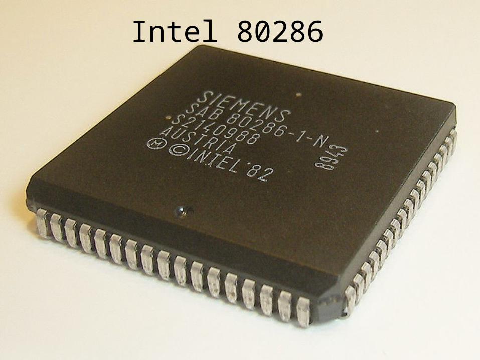
Intel 80286
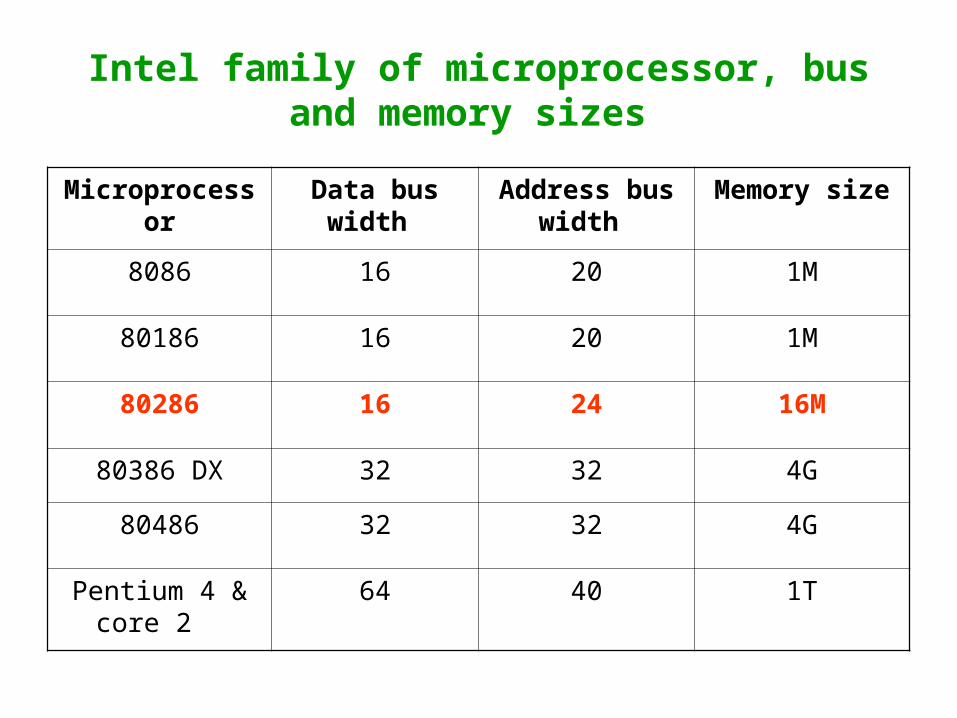
Intel family of microprocessor, bus and memory sizes
Microprocessor Data bus width
Address bus width
Memory size
8086 16 20 1M
80186 16 20 1M
80286 16 24 16M
80386 DX 32 32 4G
80486 32 32 4G
Pentium 4 & core 2
64 40 1T

Salient features of 80286
80286 is the first member of the family of advanced microprocessors with memory management and protection abilities
The 80286 CPU, with its 24-bit address bus is able to address 16Mb of physical memory.
Available in 12.5Mhz, 10MHz & 8Mhz clock frequencies
Memory management , virtual memory management & protection abilities.
Memory management is supported by a hardware unit called Memory management unit.
Intel’s 80286 is the first CPU to incorporate the Integrated memory management unit.
Function of memory management unit :1. Ensure smooth execution of the program.
2. Protection.
SWAPPING IN : From secondary memory to physical memory

SWAPPING OUT :From physical memory to secondary memory
2. Important aspect of memory management is Data Protection or unauthorized access prevention.
– Done with the help of segmented memory– Prevents overlapping of segments to avoid random
result.
Operating Modes
Intel 80286 has 2 operating modes.
1. Real address mode.
2. Protected Virtual address mode.
Real Address Mode : 80286 just as a fast 8086 All memory management and protection mechanisms are
disabled
Protected Virtual Address Mode
80286 works with all of its memory management and protection capabilities with the advanced instruction set.
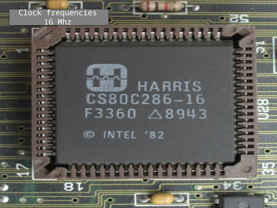
Clock frequencies 16 Mhz

Clock frequencies 10Mhz
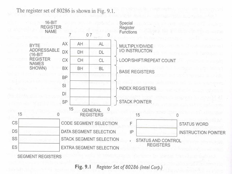
Register organization of 80286
The 80286 CPU contains almost the same set of registers, as in 8086.
1. Eight 16-bit general purpose registers.
2. Four 16 bit segment registers.
3. Status and control register.
4. Instruction pointer.
Flag Registers


The flag register bits D0,D2 , D4 ,D6 , D7 & D11 are modified according to the result of the execution of logical and arithmetic instruction. These are called Status Fag Bit.
D8 - Trap Flag (TF)
D9 - Interrupt Flag (IF)
D8 & D9 – are used to control machine operation and thus they are called Control flags.
IOPL – I/O privilege field (bit D12 and D13)
NT – Nested task flag (bit D14)
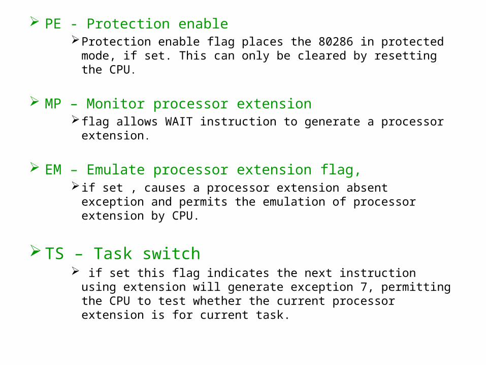
PE - Protection enableProtection enable flag places the 80286 in protected mode, if
set. This can only be cleared by resetting the CPU.
MP – Monitor processor extension flag allows WAIT instruction to generate a processor
extension.
EM – Emulate processor extension flag, if set , causes a processor extension absent exception and
permits the emulation of processor extension by CPU.
TS – Task switch if set this flag indicates the next instruction using extension
will generate exception 7, permitting the CPU to test whether the current processor extension is for current task.

Machine Status Word
• Consist of four flags. These are – PE, MP, EM and TS
• LMSW & SMSW instruction are available in the instruction set of 80286 to write and read the MSW in real address mode.

Internal Block Diagram of 80286


Functional Parts
1. Address unit
2. Bus unit
3. Instruction unit
4. Execution unit

1. Address Unit– Calculate the physical addresses of the instruction and
data that the CPU want to access– Address lines derived by this unit may be used to
address different peripherals. – Physical address computed by the address unit is
handed over to the BUS unit.
2. Bus Unit– Transmit the physical address over address bus A0 –
A23.
– Instruction Pipelining.– Prefetcher module in the bus unit performs this task of
prefetching. – Bus controller controls the prefetcher module. – Fetched instructions are arranged in a 6 – byte prefetch
queue.– Processor Extension Interface Module – Take care of
communication b/w CPU and a coprocessor.

3. Instruction Unit – Receive arranged instructions from 6 byte prefetch
queue. – Instruction decoder decodes the instruction one by one
and are latched onto a decoded instruction queue. – O/p of the decoding circuit drives a control circuit in the
Execution unit.
4. Execution unit– Control unit is responsible for executing the instructions
received from the decoded instruction queue. – Contains Register Bank.– ALU is the heart of execution unit.– After execution ALU sends the result either over data
bus or back to the register bank.

Additional Instructions of Intel 80286
Sl no
Instruction Purpose
1. CLTS Clear the task – switched bit
2. LDGT Load global descriptor table register
3. SGDT Store global descriptor table register
4. LIDT Load interrupt descriptor table register
5. SIDT Store interrupt descriptor table register
6. LLDT Load local descriptor table register
7. SLDT Store local descriptor table register
8. LMSW Load machine status register
9. SMSW Store machine status register

Sl no
Instruction Purpose
10. LAR Load access rights
11. LSL Load segment limit
12. SAR Store access right
13. ARPL Adjust requested privilege level
14. VERR Verify a read access
15. VERW Verify a write access

CLTS The clear task – switched flag instruction clears the TS
(Task - switched) flag bit to a logic 0.
LAR The load access rights Instruction reads the segment
descriptor and place a copy of the access rights byte into a 16 bit register.
LSL The load segment limit instruction Loads a user –
specified register with the segment limit.

VERRThe verify for read access instruction verifies that a
segment can de read.
VERWThe verify for write access instruction is used to verify
that a segment can be written.
ARPLThe Adjust request privilege level instruction is used to
test a selector so that the privilege level of the requested selector is not violated.