Intel 4-Mbit SmartVolt device Guide
57
E SEE NEW DESIGN RECOMMENDATIONS December 1997 Order Number: 290530-006 Intel SmartVoltage Technology 5 V or 12 V Program/Erase 2.7 V, 3.3 V or 5 V Read Operation Very High-Performance Read 5 V: 60 ns Access Time 3 V: 110 ns Access Time 2.7 V: 120 ns Access Time Low Power Consumption Max 60 mA Read Current at 5 V Max 30 mA Read Current at 2.7 V –3.6 V x8/x16-Selectable Input/Output Bus 28F400 for High Performance 16- or 32-bit CPUs x8-Only Input/Output Architecture 28F004B for Space-Constrained 8-bit Applications Optimized Array Blocking Architecture One 16-KB Protected Boot Block Two 8-KB Parameter Blocks 96-KB and 128-KB Main Blocks Top or Bottom Boot Locations Extended Temperature Operation –40 °C to +85 °C Extended Block Erase Cycling 100,000 Cycles at Commercial Temp 10,000 Cycles at Extended Temp Automated Word/Byte Program and Block Erase Command User Interface Status Registers Erase Suspend Capability SRAM-Compatible Write Interface Automatic Power Savings Feature Reset/Deep Power-Down Input 0.2 µA I CC Typical Provides Reset for Boot Operations Hardware Data Protection Feature Absolute Hardware-Protection for Boot Block Write Lockout during Power Transitions Industry-Standard Surface Mount Packaging 40-, 48-, 56-Lead TSOP 44-Lead PSOP Footprint Upgradeable from 2-Mbit and to 8-Mbit Boot Block Flash Memories ETOX™ IV Flash Technology New Design Recommendations: For new 2.7 V –3.6 V VCC designs with this device, Intel recommends using the Smart 3 Advanced Boot Block. Reference Smart 3 Advanced Boot Block 4-Mbit, 8-Mbit, 16-Mbit Flash Memory Family datasheet, order number 290580. For new 5 V VCC designs with this device, Intel recommends using the 4-Mbit Smart 5 Boot Block. Reference Smart 5 Flash Memory Family 2, 4, 8 Mbit datasheet, order number 290599. These documents are also available at Intel’s website, http://www.intel.co m/design/flcomp. REFERENCE ONLY 4-MBIT SmartVoltage BOOT BLOCK FLASH MEMORY FAMILY 28F400BV-T/B, 28F400CV-T/B, 28F004BV-T/B 28F400CE-T/B, 28F004BE-T/B
-
Upload
userscrybd -
Category
Documents
-
view
222 -
download
0
Transcript of Intel 4-Mbit SmartVolt device Guide

8/12/2019 Intel 4-Mbit SmartVolt device Guide
http://slidepdf.com/reader/full/intel-4-mbit-smartvolt-device-guide 1/57
E SEE NEW DESIGN RECOMMENDATIONS
December 1997 Order Number: 290530-006
Intel SmartVoltage Technology 5 V or 12 V Program/Erase 2.7 V, 3.3 V or 5 V Read Operation
Very High-Performance Read 5 V: 60 ns Access Time 3 V: 110 ns Access Time 2.7 V: 120 ns Access Time
Low Power Consumption Max 60 mA Read Current at 5 V Max 30 mA Read Current at
2.7 V –3.6 V
x8/x16-Selectable Input/Output Bus 28F400 for High Performance 16- or32-bit CPUs
x8-Only Input/Output Architecture 28F004B for Space-Constrained
8-bit Applications
Optimized Array Blocking Architecture One 16-KB Protected Boot Block Two 8-KB Parameter Blocks 96-KB and 128-KB Main Blocks Top or Bottom Boot Locations
Extended Temperature Operation –40 °C to +85 °C
Extended Block Erase Cycling 100,000 Cycles at Commercial Temp 10,000 Cycles at Extended Temp
Automated Word/Byte Program andBlock Erase Command User Interface Status Registers Erase Suspend Capability
SRAM-Compatible Write Interface
Automatic Power Savings Feature
Reset/Deep Power-Down Input
0.2 µA ICCTypical Provides Reset for Boot Operations
Hardware Data Protection Feature Absolute Hardware-Protection for
Boot Block Write Lockout during Power
Transitions
Industry-Standard Surface MountPackaging 40-, 48-, 56-Lead TSOP 44-Lead PSOP
Footprint Upgradeable from 2-Mbit andto 8-Mbit Boot Block Flash Memories
ETOX™ IV Flash Technology
New Design Recommendations:
For new 2.7 V –3.6 V VCC designs with this device, Intel recommends using the Smart 3 Advanced BootBlock. Reference Smart 3 Advanced Boot Block 4-Mbit, 8-Mbit, 16-Mbit Flash Memory Family datasheet,order number 290580.
For new 5 V VCC designs with this device, Intel recommends using the 4-Mbit Smart 5 Boot Block. ReferenceSmart 5 Flash Memory Family 2, 4, 8 Mbit datasheet, order number 290599.
These documents are also available at Intel’s website, http://www.intel.com/design/flcomp.
REFERENCE ONLY
4-MBIT SmartVoltage BOOT BLOCK
FLASH MEMORY FAMILY
28F400BV-T/B, 28F400CV-T/B, 28F004BV-T/B
28F400CE-T/B, 28F004BE-T/B

8/12/2019 Intel 4-Mbit SmartVolt device Guide
http://slidepdf.com/reader/full/intel-4-mbit-smartvolt-device-guide 2/57
Information in this document is provided in connection with Intel products. No license, express or implied, by estoppel orotherwise, to any intellectual property rights is granted by this document. Except as provided in Intel’s Terms and Conditions ofSale for such products, Intel assumes no liability whatsoever, and Intel disclaims any express or implied warranty, relating tosale and/or use of Intel products including liability or warranties relating to fitness for a particular purpose, merchantability, orinfringement of any patent, copyright or other intellectual property right. Intel products are not intended for use in medical, lifesaving, or life sustaining applications.
Intel may make changes to specifications and product descriptions at any time, without notice.
The 28F400BV-T/B, 28F400CV-T/B, 28F004BV-T/B, 28F400CE-T/B, 28F004BE-T/B may contain design defects or errorsknown as errata which may cause the product to deviate from published specifications. Current characterized errata areavailable on request.
Contact your local Intel sales office or your distributor to obtain the latest specifications and before placing your product order.
Copies of documents which have an ordering number and are referenced in this document, or other Intel literature, may beobtained from:
Intel CorporationP.O. Box 5937Denver, CO 80217-9808
or call 1-800-548-4725or visit Intel’s Website at http:\\www. intel.com
COPYRIGHT © INTEL CORPORATION, 1997 CG-041493
*Third-party brands and names are the property of their respective owners.

8/12/2019 Intel 4-Mbit SmartVolt device Guide
http://slidepdf.com/reader/full/intel-4-mbit-smartvolt-device-guide 3/57
E 4-MBIT SmartVoltage BOOT BLOCK FAMILY
3SEE NEW DESIGN RECOMMENDATIONS
CONTENTS
PAGE PAGE
1.0 PRODUCT FAMILY OVERVIEW.....................51.1 New Features in the SmartVoltage Products5
1.2 Main Features..............................................5
1.3 Applications..................................................7
1.4 Pinouts.........................................................7
1.5 Pin Descriptions .........................................11
2.0 PRODUCT DESCRIPTION............................13
2.1 Memory Blocking Organization...................13
2.1.1 One 16-KB Boot Block.........................13
2.1.2 Two 8-KB Parameter Blocks................13
2.1.3 One 96-KB + Three 128-KB MainBlocks ................................................13
3.0 PRODUCT FAMILY PRINCIPLES OFOPERATION ................................................15
3.1 Bus Operations ..........................................15
3.2 Read Operations........................................15
3.2.1 Read Array..........................................15
3.2.2 Intelligent Identifiers ............................17
3.3 Write Operations ........................................17
3.3.1 Command User Interface (CUI) ...........17
3.3.2 Status Register....................................20
3.3.3 Program Mode.....................................21
3.3.4 Erase Mode.........................................21
3.4 Boot Block Locking ....................................22
3.4.1 VPP = VIL for Complete Protection.......22
3.4.2 WP# = VIL for Boot Block Locking .......223.4.3 RP# = VHH or WP# = VIH for
Boot Block Unlocking .........................22
3.4.4 Upgrade Note for 8-Mbit 44-PSOPPackage .............................................22
3.5 Power Consumption...................................26
3.5.1 Active Power .......................................26
3.5.2 Automatic Power Savings (APS) .........26
3.5.3 Standby Power ....................................26
3.5.4 Deep Power-Down Mode.....................26
3.6 Power-Up/Down Operation.........................26
3.6.1 RP# Connected to System Reset ........26
3.6.2 VCC, VPP and RP# Transitions .............27
3.7 Power Supply Decoupling ..........................27
3.7.1 VPP Trace on Printed Circuit Boards ....27
4.0 ELECTRICAL SPECIFICATIONS..................28
4.1 Absolute Maximum Ratings........................28
4.2 Commercial Operating Conditions..............28
4.2.1 Applying VCC Voltages.........................28
4.3 Capacitance ...............................................29
4.4 DC Characteristics —Commercial ...............30
4.5 AC Characteristics—Read OnlyOperations—Commercial ..........................34
4.6 AC Characteristics—WE# Controlled WriteOperations—Commercial ..........................37
4.7 AC Characteristics—CE# Controlled WriteOperations—Commercial ..........................40
4.8 Erase and Program Timings—Commercial.43
4.9 Extended Operating Conditions..................43
4.9.1 Applying VCC Voltages.........................44
4.10 Capacitance .............................................44
4.11 DC Characteristics—ExtendedTemperature Operations............................45
4.12 AC Characteristics—Read OnlyOperations—Extended Temperature .........51
4.13 AC Characteristics—WE# Controlled WriteOperations—Extended Temperature .........52
4.14 AC Characteristics—CE# Controlled WriteOperations—Extended Temperature .........54
4.15 Erase and Program Timings—ExtendedTemperature..............................................55
5.0 ORDERING INFORMATION..........................56
6.0 ADDITIONAL INFORMATION.......................57
Related Intel Information ..................................57

8/12/2019 Intel 4-Mbit SmartVolt device Guide
http://slidepdf.com/reader/full/intel-4-mbit-smartvolt-device-guide 4/57
4-MBIT SmartVoltage BOOT BLOCK FAMILY E
4 SEE NEW DESIGN RECOMMENDATIONS
REVISION HISTORY
Number Description
-001 Initial release of datasheet.
-002 Status changed from Product Preview to Preliminary28F400CV/CE/BE references and information added throughout.
2.7 V CE/BE specs added throughout.The following sections have been changed or rewritten: 1.1, 3.0, 3.2.1, 3.2.2, 3.3.1,
3.3.1.1, 3.3.2, 3.3.2.1, 3.3.3, 3.3.4, 3.6.2.Note 2 added to Figure 3 to clarify 28F008B pinout vs. 28F008SA.Sentence about program and erase WSM timeout deleted from Section 3.3.3, 3.3.4.Erroneous arrows leading out of error states deleted from flowcharts in Figs. 9, 10.Sections 5.1, 6.1 changed to “Applying VCC Voltages.” These sections completely
changed to clarify VCC ramp requirements.IPPD 3.3 V Commercial spec changed from 10 to 5 µA.Capacitance tables added after commercial and extended DC Characteristics tables.Test and slew rate notes added to Figs. 12, 13, 19, 20, 21.Test configuration drawings (Fig. 14, 22) consolidated into one, with component
values in table. (Component values also rounded off).tELFL, tELFH, tAVFL changed from 7 to 5 ns for 3.3 V BV-60 commercial and 3.3 V
TBV-80 extended, 10 to 5 ns for 3.3 V BV-80 and BV-120 commercial.tWHAX and tEHAX changed from 10 to 0 ns.tPHWL changed from 1000 ns to 800 ns for 3.3 V BV-80, BV-120 commercial.tPHEL changed from 1000 ns to 800 ns for 3.3 V BV-60, BV-80, and BV-120 commercial.
-003 28F400BE row removed from Table 1Applying VCC voltages (Sections 5.1 and 6.1) rewritten for clarity.Minor cosmetic changes/edits.
-004 Corrections: Spec typographical error “tQWL” corrected to read “tQVVL.”Intel386™ EX Microprocessor block diagram updated because latest Intel386 CPUspecs require less glue logic.Spec tELFL and tELFH changed from 5 ns (max) to 0 ns (min).New specs tPLPH and tPLQX added from Specification Update document (297595).Specs tEHQZ and tGHQZ improved on most voltage/speed combinations.
-005 Correction: Appendix A, Ordering information fixed order numbers from TE27F400BVT80to TE28F400BVT80 and TE27F400BVB80 to TE28F400BVB80.Updated disclaimer.
-006 Added New Design Recommendations section to cover page.Updated Erase Suspend/Resume Flowchart .

8/12/2019 Intel 4-Mbit SmartVolt device Guide
http://slidepdf.com/reader/full/intel-4-mbit-smartvolt-device-guide 5/57
E 4-MBIT SmartVoltage BOOT BLOCK FAMILY
5SEE NEW DESIGN RECOMMENDATIONS
1.0 PRODUCT FAMILY OVERVIEW
This datasheet contains the specifications for thetwo branches of products in the SmartVoltage4-Mbit boot block flash memory family: the -BE/CEsuffix products feature a low VCC operating rangeof 2.7 V –3.6 V; the -BV/CV suffix products offer3.0 V–3.6 V operation. Both BE/CE and BV/CVproducts also operate at 5 V for high-speed
access times. Throughout this datasheet, the28F400 refers to all x8/x16 4-Mbit products, while28F004B refers to all x8 4-Mbit boot blockproducts. Also, the term “2.7 V” generally refers tothe full voltage range 2.7 V–3.6 V. Section 1.0provides an overview of the flash memory familyincluding applications, pinouts and pindescriptions. Sections 2.0 and 3.0 describe thememory organization and operation for theseproducts. Section 4.0 contains the family’soperating specifications. Finally, Sections 5.0 and6.0 provide ordering and document referenceinformation.
1.1 New Features in theSmartVoltage Products
The SmartVoltage boot block flash memory familyoffers identical operation with the BX/BL 12 Vprogram products, except for the differences listedbelow. All other functions are equivalent to currentproducts, including signatures, Write commands,and pinouts.
• WP# pin has replaced a DU (Don’t Use) pin.
Connect the WP# pin to control signal or to
VCC or GND (in this case, a logic-level signal
can be placed on DU pin). See Tables 2 and 9
to see how the WP# pin works.
• 5 V program/erase operation has been added.
If switching VPP for write protection, switch to
GND (not 5 V) for complete write protection.
To take advantage of 5 V write-capability,
allow for connecting 5 V to VPP and
disconnecting 12 V from VPP line.
• Enhanced circuits optimize low VCC
performance, allowing operation down to
VCC = 2.7 V (using the BE product).
If you are using BX/BL 12 V VPP boot blockproducts today, you should account for thedifferences listed above and also allow forconnecting 5 V to VPP and disconnecting 12 Vfrom VPP line, if 5 V writes are desired.
1.2 Main Features
Intel’s SmartVoltage technology is the mostflexible voltage solution in the flash industry,providing two discrete voltage supply pins: VCC forread operation, and VPP for program and eraseoperation. Discrete supply pins allow systemdesigners to use the optimal voltage levels fortheir design. The 28F400BV/CV, 28F004BV,28F400CE and 28F004BE provide program/erasecapability at 5 V or 12 V. The 28F400BV/CV and28F004BV allow reads with VCC at 3.3 ± 0.3 V or5 V, while the 28F400CE and 28F004BE allowreads with VCC at 2.7 V–3.6 V or 5 V. Since manydesigns read from the flash memory a largepercentage of the time, read operation using the2.7 V or 3.3 V ranges can provide great powersavings. If read performance is an issue, however,5 V VCC provides faster read access times.
Table 1. SmartVoltage Provides Total Voltage Flexibility
Product Bus VCC VPP
Name Width 2.7 V –3.6 V 3.3 ± 0.3 V 5 V ± 5%5 V ± 10%
5 V ± 10% 12 V ± 5%
28F004BV-T/B x8 √ √ √ √
28F400BV-T/B x8 or x16 √ √ √ √
28F400CV-T/B x8 or x16 √ √ √ √
28F004BE-T/B x8 √ √ √ √
28F400CE-T/B x8 or x16 √ √ √ √

8/12/2019 Intel 4-Mbit SmartVolt device Guide
http://slidepdf.com/reader/full/intel-4-mbit-smartvolt-device-guide 6/57

8/12/2019 Intel 4-Mbit SmartVolt device Guide
http://slidepdf.com/reader/full/intel-4-mbit-smartvolt-device-guide 7/57
E 4-MBIT SmartVoltage BOOT BLOCK FAMILY
7SEE NEW DESIGN RECOMMENDATIONS
1.3 Applications
The 4-Mbit boot block flash memory familycombines high-density, low-power, high-performance, cost-effective flash memories withblocking and hardware protection capabilities. Theirflexibility and versatility reduce costs throughout theproduct life cycle. Flash memory is ideal for Just-In-Time production flow, reducing system inventory
and costs, and eliminating component handlingduring the production phase.
When your product is in the end-user’s hands, andupdates or feature enhancements becomenecessary, flash memory reduces the update costsby allowing user-performed code changes insteadof costly product returns or technician calls.
The 4-Mbit boot block flash memory family providesfull-function, blocked flash memories suitable for awide range of applications. These applicationsinclude extended PC BIOS and ROM-ableapplications storage, digital cellular phone programand data storage, telecommunication boot/firmware,printer firmware/font storage and various otherembedded applications where program and data
storage are required.
Reprogrammable systems, such as personalcomputers, are ideal applications for the 4-Mbitflash memory products. Increasing softwaresophistication greatens the probability that a codeupdate will be required after the PC is shipped. Forexample, the emerging of “plug and play” standardin desktop and portable PCs enables auto-configuration of ISA and PCI add-in cards.However, since the plug and play specificationcontinues to evolve, a flash BIOS provides a cost-effective capability to update existing PCs. Inaddition, the parameter blocks are ideal for storingthe required auto-configuration parameters,allowing you to integrate the BIOS PROM andparameter storage EEPROM into a single
component, reducing parts costs while increasingfunctionality.
The 4-Mbit flash memory products are alsoexcellent design solutions for digital cellular phoneand telecommunication switching applicationsrequiring very low power consumption, high-performance, high-density storage capability,modular software designs, and a small form factorpackage. The 4-Mbit’s blocking scheme allows foreasy segmentation of the embedded code with16 Kbytes of hardware-protected boot code, four
main blocks of program code and two parameterblocks of 8 Kbytes each for frequently updated datastorage and diagnostic messages (e.g., phonenumbers, authorization codes).
Intel’s boot block architecture provides a flexiblevoltage solution for the different design needs ofvarious applications. The asymmetrically-blockedmemory map allows the integration of severalmemory components into a single flash device. Theboot block provides a secure boot PROM; theparameter blocks can emulate EEPROMfunctionality for parameter store with propersoftware techniques; and the main blocks providecode and data storage with access times fastenough to execute code in place, decreasing RAMrequirements.
1.4 Pinouts
Intel’s SmartVoltage Boot Block architectureprovides upgrade paths in every package pinout tothe 8-Mbit density. The 28F004B 40-lead TSOPpinout for space-constrained designs is shown inFigure 3. The 28F400 44-lead PSOP pinout followsthe industry-standard ROM/EPROM pinout, asshown in Figure 4. For designs that require x16operation but have space concerns, refer to the48-lead pinout in Figure 5. Furthermore, the 28F40056-lead TSOP pinout shown in Figure 6 providesdensity upgrades to future higher density boot blockmemories.
Pinouts for the corresponding 2-Mbit and 8-Mbitcomponents are also provided for convenientreference. 4-Mbit pinouts are given on the chipillustration in the center, with 2-Mbit and 8-Mbitpinouts going outward from the center.

8/12/2019 Intel 4-Mbit SmartVolt device Guide
http://slidepdf.com/reader/full/intel-4-mbit-smartvolt-device-guide 8/57
4-MBIT SmartVoltage BOOT BLOCK FAMILY E
8 SEE NEW DESIGN RECOMMENDATIONS
A[18:1]
CS#
RD#
WR#
D[0:15]
A[0:17]
CE#
OE#
WE#
DQ[0:15]
28F400BV-60
RP#
i386™ EX CPU(25 MHz)
RESET
RESET
0530_01
NOTE:
A data bus buffer may be needed for processor speeds above 25 MHz.
Figure 1. 28F400 Interface to Intel386™ EX Microprocessor
UCS#
80C188EB
-A15
A8
ALE
P1.X
WR#
RD#
RESIN#
System Reset
WE#OE#
VPP
ADDRESSLATCHES
LE
ADDRESSLATCHES
LE
CE#
A0
-A18
RP#
28F004-T-AD7AD0
A[16:18]
DQ0
-DQ7
WP#
VCC
10KΩ
P1.X
VCC
0530_02
Figure 2. 28F004B Interface to Intel80C188EB 8-Bit Embedded Microprocessor

8/12/2019 Intel 4-Mbit SmartVolt device Guide
http://slidepdf.com/reader/full/intel-4-mbit-smartvolt-device-guide 9/57
E 4-MBIT SmartVoltage BOOT BLOCK FAMILY
9SEE NEW DESIGN RECOMMENDATIONS
28F004BBoot Block40-Lead TSOP10 mm x 20 mm
TOP VIEW
323130
29
282726252423
2221
33
3435
363738
3940
2019
17
18
12
3
4
567
89
10
11
121314
16
15
A1
A2
A3
RP#WE#
VPP
A16A15
A7A6A5A4
A14A13
A8
A9
A11
A12
WP#
DQ7
CE#
OE#
GND
A0
DQ6
DQ5DQ4
DQ2DQ1DQ0
VCC
DQ3
A17
GND
NC
A10
NCNC
NC
28F002B 28F002B28F008B 28F008B
DQ7
CE#
OE#
GND
A0
DQ6
DQ5DQ4
DQ2DQ1DQ0
VCC
VCC
DQ3
A17
GND
NC
A10
NC
A1
A2
A3
RP#WE#
VPP
A16A15
A7A6A5A4
A14A13
A8
A9
A11
A12
WP#
A1
A2
A3
RP#WE#
VPP
A16A15
A7A6A5A4
A14A13
A8
A9
A11
A12
WP#A18 A18
A19
DQ7
CE#
OE#
GND
A0
DQ6
DQ5DQ4
DQ2DQ1DQ0
VCC
DQ3
A17
GND
NC
A10
NCNC
VCCVCC
0530_03
Figure 3. The 40-Lead TSOP Offers the Smallest Form Factor for Space-Constrained Applications
PA28F400Boot Block
44-Lead PSOP0.525" x 1.110"
TOP VIEW32
31
30
29
28
2726
25
2423
33
34
35
36
37
38
39
40
41
42
4344
2221
20
19
17
18
12
3
4
5
6
7
8
9
10
11
12
13
14
16
15
RP#WE#
A
A
A
A
A
A
A
A
A
BYTE#
GND
DQ /A
DQ
DQ
DQ
DQDQ
DQ
DQ
V
8
9
10
11
12
13
14
15
16
15
7
14
6
13
5
12
4
CC
-1
28F800 28F200
VPP
WP#
NC
A 7
A 6
A 5
A 4
A 3
A 2
A 1
A 0
CE#
GND
OE#
DQ0
DQ8
DQ1
DQ9
DQ2
DQ10
DQ3
DQ11
VPP
A17
A 7
A 6
A 5
A 4
A 3
A 2
A 1
A 0
CE#
GND
OE#
DQ0
DQ8
DQ1
DQ9
DQ2
DQ10
DQ3
DQ11
A18
VPP
WP#
A17
A 7
A 6
A 5
A 4
A 3
A 2
A 1
A 0
CE#
GND
OE#
DQ0
DQ8
DQ1
DQ9
DQ2
DQ10
DQ3
DQ11
RP#WE#
A
A
A
A
A
A
A
A
A
BYTE#
GND
DQ /A
DQ
DQ
DQ
DQDQ
DQ
DQ
V
8
9
10
11
12
13
14
15
16
15
7
14
6
13
5
12
4
CC
-1
RP#WE#
A
A
A
A
A
A
A
A
A
BYTE#
GND
DQ /A
DQ
DQ
DQ
DQDQ
DQ
DQ
V
8
9
10
11
12
13
14
15
16
15
7
14
6
13
5
12
4
CC
-1
28F80028F200
0530_04
NOTE: Pin 2 is WP# on 2- and 4-Mbit devices but A18 on the 8-Mbit because no other pins were available for the high orderaddress. Thus, the 8-Mbit in the 44-lead PSOP cannot unlock the boot block without RP# = VHH (12 V). To allow upgrades tothe 8 Mbit from 2/2 Mbit in this package, design pin 2 to control WP# at the 2/4 Mbit level and A18 at the 8-Mbit density. SeeSection 3.4 for details.
Figure 4. The 44-Lead PSOP Offers a Convenient Upgrade from JEDEC ROM Standards

8/12/2019 Intel 4-Mbit SmartVolt device Guide
http://slidepdf.com/reader/full/intel-4-mbit-smartvolt-device-guide 10/57
4-MBIT SmartVoltage BOOT BLOCK FAMILY E
10 SEE NEW DESIGN RECOMMENDATIONS
28F400
Boot Block48-Lead TSOP
12 mm x 20 mm
TOP VIEW333435363738
39404142
4344454647
48
2423
22
2120
19
17
18
1234
56789
10
11121314
1615
25
2627
28
2930
3132
16
15 -1
7
14
6
13
5
12
4
ABYTE#GNDDQ /ADQDQDQDQDQDQ
DQ
DQV
DQ
DQDQDQ
DQDQDQ
OE#GNDCE#
A
CC
11
3
10
2
9
1
8
0
0
16
15 -1
7
14
6
13
5
12
4
ABYTE#GNDDQ /ADQDQDQDQDQDQ
DQ
DQV
DQ
DQDQDQ
DQDQDQ
OE#GNDCE#
A
CC
11
3
10
2
9
1
8
0
0
28F80028F200
16
15 -1
7
14
6
13
5
12
4
ABYTE#GNDDQ /ADQDQDQDQDQDQ
DQ
DQDQ
DQDQDQ
DQDQDQ
OE#GNDCE#
A
V CC
11
3
10
2
9
1
8
0
0
28F20028F800
A
AA
AAA
AANCNC
WE#RP#
WP#NC
A
AAA
AAA
A
17
7
6
5
4
3
2
1
15
14
13
12
11
10
9
8
A
AA
AAA
AANCNC
WE#RP#
WP#NCNC
AAA
AAA
A
7
6
5
4
3
2
1
15
14
13
12
11
10
9
8
A
AA
AAA
AANCNC
WE#RP#
WP#NCNCA
AAA
AAA
A
17
7
6
5
4
3
2
1
15
14
13
12
11
10
9
8
V PP VPP VPP
A18
NC
0530_05
Figure 5. The 48-Lead TSOP Offers the Smallest Form Factor for x16 Operation
28F40056-Lead TSOP
Boot Block14 mm x 20 mm
TOP VIEW
2827
26252423
222120
19
17
18
1234
56789
10
11121314
1615
A1
A2
A3
RP#WE#
A15
A7A6A5A4
A14A13
A8
A9
A11
A12
NC
VPP
NCNC
NCNC
NC
NC
A10
WP#NC
NC
A1
A2
A3
RP#WE#
A15
A7A6A5A4
A14A13
A8
A9
A11
A12
NC
VPP
NCNC
NCNC
NC
NC
A10
WP#NC
DQ7
CE#
OE#
GND
A0
DQ6
DQ5
DQ4
DQ2
DQ1
DQ0
VCC
VCC
DQ3
GND
NCNC
DQ9
DQ10
DQ11
DQ8
BYTE#
DQ15 /A-1
DQ14
DQ13
DQ12
A16NC
28F200 28F200
A17
4142434445464748
495051
5253545556
32313029
33
3435
3637
38
3940
DQ7
CE#
OE#
GND
A0
DQ6
DQ5
DQ4
DQ2
DQ1
DQ0
VCC
VCC
DQ3
GND
NCNC
DQ9
DQ10
DQ11
DQ8
BYTE#
DQ15 /A-1
DQ14
DQ13
DQ12
A16NC
0530_06
Figure 6. The 56-Lead TSOP Offers Compatibility between 2 and 4 Mbits

8/12/2019 Intel 4-Mbit SmartVolt device Guide
http://slidepdf.com/reader/full/intel-4-mbit-smartvolt-device-guide 11/57
E 4-MBIT SmartVoltage BOOT BLOCK FAMILY
11SEE NEW DESIGN RECOMMENDATIONS
1.5 Pin Descriptions
Table 2. 28F400/004 Pin Descriptions
Symbol Type Name and Function
A0 –A18 INPUT ADDRESS INPUTS for memory addresses. Addresses are internally latchedduring a write cycle. The 28F400 only has A0 – A17 pins, while the 28F004B hasA0 – A18.
A9 INPUT ADDRESS INPUT: When A9 is at VHH the signature mode is accessed. During
this mode, A0 decodes between the manufacturer and device IDs. When BYTE#is at a logic low, only the lower byte of the signatures are read. DQ 15 /A –1 is adon’t care in the signature mode when BYTE# is low.
DQ0 –DQ7 INPUT/ OUTPUT
DATA INPUTS/OUTPUTS: Inputs array data on the second CE# and WE# cycleduring a Program command. Inputs commands to the CUI when CE# and WE#are active. Data is internally latched during the write cycle. Outputs array,intelligent identifier and status register data. The data pins float to tri-state whenthe chip is de-selected or the outputs are disabled.
DQ8 –DQ15 INPUT/ OUTPUT
DATA INPUTS/OUTPUTS: Inputs array data on the second CE# and WE# cycleduring a Program command. Data is internally latched during the write cycle.Outputs array data. The data pins float to tri-state when the chip is de-selected orthe outputs are disabled as in the byte-wide mode (BYTE# = “0”). In the byte-widemode DQ15 /A –1 becomes the lowest order address for data output on DQ0 –DQ7.The 28F004B does not include these DQ8 –DQ15 pins.
CE# INPUT CHIP ENABLE: Activates the device’s control logic, input buffers, decoders and
sense amplifiers. CE# is active low. CE# high de-selects the memory device andreduces power consumption to standby levels. If CE# and RP# are high, but notat a CMOS high level, the standby current will increase due to current flowthrough the CE# and RP# input stages.
OE# INPUT OUTPUT ENABLE: Enables the device’s outputs through the data buffers duringa read cycle. OE# is active low.
WE# INPUT WRITE ENABLE: Controls writes to the command register and array blocks. WE#is active low. Addresses and data are latched on the rising edge of the WE#pulse.
RP# INPUT RESET/DEEP POWER-DOWN: Uses three voltage levels (V IL, VIH, and VHH) tocontrol two different functions: reset/deep power-down mode and boot blockunlocking. It is backwards-compatible with the BX/BL/BV products.
When RP# is at logic low, the device is in reset/deep power-down mode,which puts the outputs at High-Z, resets the Write State Machine, and draws
minimum current.
When RP# is at logic high, the device is in standard operation. When RP#transitions from logic-low to logic-high, the device defaults to the read array mode.
When RP# is at VHH, the boot block is unlocked and can be programmed orerased. This overrides any control from the WP# input.

8/12/2019 Intel 4-Mbit SmartVolt device Guide
http://slidepdf.com/reader/full/intel-4-mbit-smartvolt-device-guide 12/57
4-MBIT SmartVoltage BOOT BLOCK FAMILY E
12 SEE NEW DESIGN RECOMMENDATIONS
Table 2. 28F400/004 Pin Descriptions (Continued)
Symbol Type Name and Function
WP# INPUT WRITE PROTECT: Provides a method for unlocking the boot block in a systemwithout a 12 V supply.
When WP# is at logic low, the boot block is locked, preventing program anderase operations to the boot block. If a program or erase operation is attemptedon the boot block when WP# is low, the corresponding status bit (bit 4 for
program, bit 5 for erase) will be set in the status register to indicate the operationfailed.
When WP# is at logic high, the boot block is unlocked and can beprogrammed or erased.
NOTE: This feature is overridden and the boot block unlocked when RP# is atVHH. See Section 3.4 for details on write protection.
BYTE# INPUT BYTE# ENABLE: Not available on 28F004B. Controls whether the deviceoperates in the byte-wide mode (x8) or the word-wide mode (x16). BYTE# pinmust be controlled at CMOS levels to meet the CMOS current specification in thestandby mode.
When BYTE# is at logic low, the byte-wide mode is enabled , where data isread and programmed on DQ0 –DQ7 and DQ15 /A –1 becomes the lowest orderaddress that decodes between the upper and lower byte. DQ8 –DQ14 are tri-statedduring the byte-wide mode.
When BYTE# is at logic high, the word-wide mode is enabled, where data isread and programmed on DQ0 –DQ15.
VCC DEVICE POWER SUPPLY: 5.0 V ± 10%, 3.3 ± 0.3 V, 2.7 V–3.6 V (BE/CE only)
VPP PROGRAM/ERASE POWER SUPPLY: For erasing memory array blocks orprogramming data in each block, a voltage either of 5 V ± 10% or 12 V ± 5% mustbe applied to this pin. When VPP < VPPLK all blocks are locked and protectedagainst Program and Erase commands.
GND GROUND: For all internal circuitry.
NC NO CONNECT: Pin may be driven or left floating.

8/12/2019 Intel 4-Mbit SmartVolt device Guide
http://slidepdf.com/reader/full/intel-4-mbit-smartvolt-device-guide 13/57
E 4-MBIT SmartVoltage BOOT BLOCK FAMILY
13SEE NEW DESIGN RECOMMENDATIONS
2.0 PRODUCT DESCRIPTION
2.1 Memory Blocking Organization
This product family features an asymmetrically-blocked architecture providing system memoryintegration. Each erase block can be erasedindependently of the others up to 100,000 times for
commercial temperature or up to 10,000 times forextended temperature. The block sizes have beenchosen to optimize their functionality for commonapplications of nonvolatile storage. The combinationof block sizes in the boot block architecture allowthe integration of several memories into a singlechip. For the address locations of the blocks, seethe memory maps in Figures 4 and 5.
2.1.1 ONE 16-KB BOOT BLOCK
The boot block is intended to replace a dedicatedboot PROM in a microprocessor or microcontroller-based system. The 16-Kbyte (16,384 bytes) bootblock is located at either the top (denoted by -Tsuffix) or the bottom (-B suffix) of the address map
to accommodate different microprocessor protocolsfor boot code location. This boot block featureshardware controllable write-protection to protect thecrucial microprocessor boot code from accidentalmodification. The protection of the boot block iscontrolled using a combination of the VPP, RP#, andWP# pins, as is detailed in Section 3.4.
2.1.2 TWO 8-KB PARAMETER BLOCKS
The boot block architecture includes parameterblocks to facilitate storage of frequently updatedsmall parameters that would normally require anEEPROM. By using software techniques, the byte-rewrite functionality of EEPROMs can be emulated.These techniques are detailed in Intel’s applicationnote, AP-604 Using Intel’s Boot Block Flash
Memory Parameter Blocks to Replace EEPROM .Each boot block component contains two parameterblocks of 8 Kbytes (8,192 bytes) each. Theparameter blocks are not write-protectable.
2.1.3 ONE 96-KB + THREE 128-KBMAIN BLOCKS
After the allocation of address space to the bootand parameter blocks, the remainder is divided intomain blocks for data or code storage. Each 4-Mbitdevice contains one 96-Kbyte (98,304 byte) blockand three 128-Kbyte (131,072 byte) blocks. See thememory maps for each device for more information.

8/12/2019 Intel 4-Mbit SmartVolt device Guide
http://slidepdf.com/reader/full/intel-4-mbit-smartvolt-device-guide 14/57
4-MBIT SmartVoltage BOOT BLOCK FAMILY E
14 SEE NEW DESIGN RECOMMENDATIONS
3FFFFH
3E000H3DFFFH3D000H3CFFFH3C000H
3BFFFH
30000H
20000H1FFFFH
10000H0FFFFH
00000H
2FFFFH
3FFFFH
30000H2FFFFH
20000H1FFFFH
10000H0FFFFH
04000H03FFFH03000H02FFFH02000H01FFFH
00000H
28F400-T
8-Kbyte PARAMETER BLOCK
16-Kbyte BOOT BLOCK
8-Kbyte PARAMETER BLOCK
96-Kbyte MAIN BLOCK
128-Kbyte MAIN BLOCK
128-Kbyte MAIN BLOCK
128-Kbyte MAIN BLOCK
28F400-B
8-Kbyte PARAMETER BLOCK
16-Kbyte BOOT BLOCK
8-Kbyte PARAMETER BLOCK
96-Kbyte MAIN BLOCK
128-Kbyte MAIN BLOCK
128-Kbyte MAIN BLOCK
128-Kbyte MAIN BLOCK
0530_07
NOTE: Address = A[17:0]. In x8 operation, the least significant system address should be connected to A-1. Memory maps areshown for x16 operation.
Figure 7. Word-Wide x16-Mode Memory Maps
7FFFFH
7C000H7BFFFH
7A000H79FFFH
78000H77FFFH
60000H5FFFFH
40000H3FFFFH
20000H
1FFFFH
00000H
28F004-T
128-Kbyte MAIN BLOCK
8-Kbyte PARAMETER BLOCK
16-Kbyte BOOT BLOCK
8-Kbyte PARAMETER BLOCK
96-Kbyte MAIN BLOCK
128-Kbyte MAIN BLOCK
128-Kbyte MAIN BLOCK
7FFFFH
60000H5FFFFH
40000H3FFFFH
20000H1FFFFH
08000H07FFFH
06000H05FFFH
04000H03FFFH
00000H
28F004-B
128-Kbyte MAIN BLOCK
8-Kbyte PARAMETER BLOCK
16-Kbyte BOOT BLOCK
8-Kbyte PARAMETER BLOCK
96-Kbyte MAIN BLOCK
128-Kbyte MAIN BLOCK
128-Kbyte MAIN BLOCK
0530_08
NOTE: Address = A[18:0]. These memory maps apply to the 28F004B or the 28F400 in x8 mode.
Figure 8. Byte-Wide x8-Mode Memory Maps

8/12/2019 Intel 4-Mbit SmartVolt device Guide
http://slidepdf.com/reader/full/intel-4-mbit-smartvolt-device-guide 15/57

8/12/2019 Intel 4-Mbit SmartVolt device Guide
http://slidepdf.com/reader/full/intel-4-mbit-smartvolt-device-guide 16/57
4-MBIT SmartVoltage BOOT BLOCK FAMILY E
16 SEE NEW DESIGN RECOMMENDATIONS
Table 3. Bus Operations for Word-Wide Mode (BYTE# = VIH)
Mode Notes RP# CE# OE# WE# A9 A0 VPP DQ0 –15
Read 1,2,3 VIH VIL VIL VIH X X X DOUT
Output Disable VIH VIL VIH VIH X X X High Z
Standby VIH VIH X X X X X High Z
Deep Power-Down 9 VIL X X X X X X High Z
Intelligent Identifier(Mfr)
4 VIH VIL VIL VIH VID VIL X 0089 H
Intelligent Identifier(Device)
4,5 VIH VIL VIL VIH VID VIH X SeeTable 5
Write 6,7,8 VIH VIL VIH VIL X X X DIN
Table 4. Bus Operations for Byte-Wide Mode (BYTE# = VIL)
Mode Notes RP# CE# OE# WE# A9 A0 A –1 VPP DQ0–7 DQ8–14
Read 1,2,3 VIH VIL VIL VIH X X X X DOUT High Z
Output
Disable
VIH VIL VIH VIH X X X X High Z High Z
Standby VIH VIH X X X X X X High Z High Z
Deep Power-Down
9 VIL X X X X X X X High Z High Z
IntelligentIdentifier (Mfr)
4 VIH VIL VIL VIH VID VIL X X 89H High Z
IntelligentIdentifier(Device)
4,5 VIH VIL VIL VIH VID VIH X X SeeTable
5
High Z
Write 6,7,8 VIH VIL VIH VIL X X X X DIN High Z
NOTES:
1. Refer to DC Characteristics .
2. X can be VIL
, VIH
for control pins and addresses, VPPLK
or VPPH
for VPP
.
3. See DC Characteristics for VPPLK, VPPH1, VPPH2, VHH, VID voltages.
4. Manufacturer and device codes may also be accessed via a CUI write sequence, A1 –A17 = X, A1 –A18 = X.
5. See Table 5 for device IDs.
6. Refer to Table 7 for valid DIN during a write operation.
7. Command writes for block erase or word/byte program are only executed when VPP = VPPH1 or VPPH2.
8. To write or erase the boot block, hold RP# at VHH or WP# at VIH. See Section 3.4.
9. RP# must be at GND ± 0.2 V to meet the maximum deep power-down current specified.

8/12/2019 Intel 4-Mbit SmartVolt device Guide
http://slidepdf.com/reader/full/intel-4-mbit-smartvolt-device-guide 17/57
E 4-MBIT SmartVoltage BOOT BLOCK FAMILY
17SEE NEW DESIGN RECOMMENDATIONS
3.2.2 INTELLIGENT IDENTIFIERS
To read the manufacturer and device codes, thedevice must be in intelligent identifier read mode,which can be reached using two methods: bywriting the Intelligent Identifier command (90H) orby taking the A9 pin to VID. Once in intelligentidentifier read mode, A0 = 0 outputs the manu-
facturer’s identification code and A0 = 1 outputs thedevice code. In byte-wide mode, only the lower byteof the above signatures is read (DQ15 /A –1 is a“don’t care” in this mode). See Table 5 for productsignatures. To return to read array mode, write aRead Array command (FFH).
Table 5. Intelligent Identifier Table
Product Mfr. ID Device ID
-T(Top Boot)
-B(Bottom Boot)
28F400 0089 H 4470 H 4471 H
28F004 89 H 78 H 79 H
3.3 Write Operations
3.3.1 COMMAND USER INTERFACE (CUI)
The Command User Interface (CUI) is the interfacebetween the microprocessor and the internal chipcontroller. Commands are written to the CUI using
standard microprocessor write timings. Theavailable commands are Read Array, ReadIntelligent Identifier, Read Status Register, ClearStatus Register, Erase and Program (summarizedin Tables 6 and 7). The three read modes are readarray, intelligent identifier read, and status registerread. For Program or Erase commands, the CUIinforms the Write State Machine (WSM) that a writeor erase has been requested. During the executionof a Program command, the WSM will control theprogramming sequences and the CUI will onlyrespond to status reads. During an erase cycle, theCUI will respond to status reads and erasesuspend. After the WSM has completed its task, itwill set the WSM status bit to a “1” (ready), whichindicates that the CUI can respond to its fullcommand set. Note that after the WSM has
returned control to the CUI, the CUI will stay in thecurrent command state until it receives anothercommand.
3.3.1.1 Command Function Description
Device operations are selected by writing specificcommands into the CUI. Tables 6 and 7 define theavailable commands.

8/12/2019 Intel 4-Mbit SmartVolt device Guide
http://slidepdf.com/reader/full/intel-4-mbit-smartvolt-device-guide 18/57
4-MBIT SmartVoltage BOOT BLOCK FAMILY E
18 SEE NEW DESIGN RECOMMENDATIONS
Table 6. Command Codes and Descriptions
Code Device Mode Decryption
00 Invalid/ Reserved
Unassigned commands that should not be used. Intel reserves the right to redefinethese codes for future functions.
FF Read Array Places the device in read array mode, so that array data will be output on the datapins.
40 ProgramSet-Up
Sets the CUI into a state such that the next write will latch the address and dataregisters on the rising edge and begin the program algorithm. The device thendefaults to the read status mode, where the device outputs status register datawhen OE# is enabled. To read the array, issue a Read Array command.
To cancel a program operation after issuing a Program Set-Up command, write all1’s (FFH for x8, FFFFH for x16) to the CUI. This will return to read status registermode after a standard program time without modifying array contents. If a programoperation has already been initiated to the WSM this command can not cancel thatoperation in progress.
10 AlternateProg Set-Up
(See 40H/Program Set-Up)
20 EraseSet-Up
Prepares the CUI for the Erase Confirm command. If the next command is not anErase Confirm command, then the CUI will set both the program status (SR.4) anderase status (SR.5) bits of the status register to a “1,” place the device into the
read status register state, and wait for another command without modifying arraycontents. This can be used to cancel an erase operation after the Erase Set-Upcommand has been issued. If an operation has already been initiated to the WSMthis can not cancel that operation in progress.
D0 EraseResume/
EraseConfirm
If the previous command was an Erase Set-Up command, then the CUI will latchaddress and data, and begin erasing the block indicated on the address pins.During erase, the device will respond only to the Read Status Register and EraseSuspend commands and will output status register data when OE# is toggled low.status register data is updated by toggling either OE# or CE# low.
B0 EraseSuspend
Valid only while an erase operation is in progress and will be ignored in any othercircumstance. Issuing this command will begin to suspend erase operation. Thestatus register will indicate when the device reaches erase suspend mode. In thismode, the CUI will respond only to the Read Array, Read Status Register, andErase Resume commands and the WSM will also set the WSM status bit to a “1”(ready). The WSM will continue to idle in the SUSPEND state, regardless of thestate of all input control pins except RP#, which will immediately shut down the
WSM and the remainder of the chip, if i t is made active. During a suspendoperation, the data and address latches will remain closed, but the address padsare able to drive the address into the read path. See Section 3.3.4.1.
70 Read StatusRegister
Puts the device into the read status register mode, so that reading the deviceoutputs status register data, regardless of the address presented to the device.The device automatically enters this mode after program or erase has completed.This is one of the two commands that is executable while the WSM is operating.See Section 3.3.2.

8/12/2019 Intel 4-Mbit SmartVolt device Guide
http://slidepdf.com/reader/full/intel-4-mbit-smartvolt-device-guide 19/57
E 4-MBIT SmartVoltage BOOT BLOCK FAMILY
19SEE NEW DESIGN RECOMMENDATIONS
Table 6. Command Codes and Descriptions (Continued)
Code Device Mode Decryption
50 Clear StatusRegister
The WSM can only set the program status and erase status bits in the statusregister to “1;” it cannot clear them to “0.”
The status register operates in this fashion for two reasons. The first is to give thehost CPU the flexibility to read the status bits at any time. Second, when
programming a string of bytes, a single status register query after programming thestring may be more efficient, since it will return the accumulated error status of theentire string. See Section 3.3.2.1.
90 Intelligent
Identifier
Puts the device into the intelligent identifier read mode, so that reading the device
will output the manufacturer and device codes. (A0 = 0 for manufacturer,
A0 = 1 for device, all other address inputs are ignored). See Section 3.2.2.
Table 7. Command Bus Definitions
First Bus Cycle Second Bus Cycle
Command Note Oper Addr Data Oper Addr Data
Read Array 8 Write X FFH
Intelligent Identifier 1 Write X 90H Read IA IID
Read Status Register 2,4 Write X 70H Read X SRD
Clear Status Register 3 Write X 50H
Word/Byte Program Write PA 40H Write PA PD
Alternate Word/ByteProgram
6,7 Write PA 10H Write PA PD
Block Erase/Confirm 6,7 Write BA 20H Write BA D0H
Erase Suspend 5 Write X B0H
Erase Resume Write X D0H
ADDRESS DATA
BA = Block Address SRD = Status Register Data
IA = Identifier Address IID = Identifier Data
PA = Program Address PD = Program Data
X = Don’t Care
NOTES:
1. Bus operations are defined in Tables 3 and 4.
2. IA = Identifier Address: A0 = 0 for manufacturer code, A0 = 1 for device code.
3. SRD - Data read from status register.
4. IID = Intelligent Identifier Data. Following the Intelligent Identifier command, two read operations access manufacturer anddevice codes.
5. BA = Address within the block being erased.
6. PA = Address to be programmed. PD = Data to be programmed at location PA.
7. Either 40H or 10H commands is valid.
8. When writing commands to the device, the upper data bus [DQ8 –DQ15] = X (28F400 only) which is either VIL or VIH, tominimize current draw.

8/12/2019 Intel 4-Mbit SmartVolt device Guide
http://slidepdf.com/reader/full/intel-4-mbit-smartvolt-device-guide 20/57
4-MBIT SmartVoltage BOOT BLOCK FAMILY E
20 SEE NEW DESIGN RECOMMENDATIONS
Table 8. Status Register Bit Definition
WSMS ESS ES DWS VPPS R R R
7 6 5 4 3 2 1 0
NOTES:
SR.7 = WRITE STATE MACHINE STATUS
1 = Ready (WSMS)
0 = Busy
Check WSM bit first to determine Word/Byte
program or Block Erase completion, before
checking program or erase status bits.
SR.6 = ERASE-SUSPEND STATUS (ESS)
1 = Erase Suspended
0 = Erase In Progress/Completed
When erase suspend is issued, WSM halts
execution and sets both WSMS and ESS bits to
“1.” ESS bit remains set to “1” until an Erase
Resume command is issued.
SR.5 = ERASE STATUS (ES)
1 = Error In Block Erasure
0 = Successful Block Erase
When this bit is set to “1,” WSM has applied the
max number of erase pulses to the block and is
still unable to verify successful block erasure.
SR.4 = PROGRAM STATUS (DWS)
1 = Error in Byte/Word Program
0 = Successful Byte/Word Program
When this bit is set to “1,” WSM has attempted
but failed to program a byte or word.
SR.3 = VPP STATUS (VPPS)
1 = VPP Low Detect, Operation Abort0 = VPP OK
The VPP status bit does not provide continuous
indication of VPP level. The WSM interrogates VPPlevel only after the Byte Write or Erase command
sequences have been entered, and informs the
system if VPP has not been switched on. The VPP
status bit is not guaranteed to report accurate
feedback between VPPLK and VPPH.
SR.2-SR.0 = RESERVED FOR FUTURE
ENHANCEMENTS (R)
These bits are reserved for future use and should
be masked out when polling the status register.
3.3.2 STATUS REGISTER
The device status register indicates when aprogram or erase operation is complete, and thesuccess or failure of that operation. To read thestatus register write the Read Status (70H)
command to the CUI. This causes all subsequentread operations to output data from the statusregister until another command is written to theCUI. To return to reading from the array, issue aRead Array (FFH) command.
The status register bits are output on DQ0 –DQ7, inboth byte-wide (x8) or word-wide (x16) mode. In theword-wide mode the upper byte, DQ8 –DQ15,outputs 00H during a Read Status command. In thebyte-wide mode, DQ8 –DQ14 are tri-stated andDQ15 /A –1 retains the low order address function.
Important: The contents of the status registerare latched on the falling edge of OE# or CE#,whichever occurs last in the read cycle. Thisprevents possible bus errors which might occur ifstatus register contents change while being read.
CE# or OE# must be toggled with each subsequentstatus read, or the status register will not indicatecompletion of a program or erase operation.
When the WSM is active, the SR.7 register willindicate the status of the WSM, and will also holdthe bits indicating whether or not the WSM wassuccessful in performing the desired operation.

8/12/2019 Intel 4-Mbit SmartVolt device Guide
http://slidepdf.com/reader/full/intel-4-mbit-smartvolt-device-guide 21/57
E 4-MBIT SmartVoltage BOOT BLOCK FAMILY
21SEE NEW DESIGN RECOMMENDATIONS
3.3.2.1 Clearing the Status Register
The WSM sets status bits 3 through 7 to “1,” andclears bits 6 and 7 to “0,” but cannot clear statusbits 3 through 5 to “0.” Bits 3 through 5 can only becleared by the controlling CPU through the use ofthe Clear Status Register (50H) command, becausethese bits indicate various error conditions. Byallowing the system software to control the resetting
of these bits, several operations may be performed(such as cumulatively programming several bytesor erasing multiple blocks in sequence) beforereading the status register to determine if an erroroccurred during that series. Clear the status registerbefore beginning another command or sequence.Note, again, that a Read Array command must beissued before data can be read from the memory orintelligent identifier.
3.3.3 PROGRAM MODE
Programming is executed using a two-writesequence. The Program Set-Up command is writtento the CUI followed by a second write whichspecifies the address and data to be programmed.The WSM will execute a sequence of internallytimed events to:
1. Program the desired bits of the addressed
memory word or byte.
2. Verify that the desired bits are sufficiently
programmed.
Programming of the memory results in specific bitswithin a byte or word being changed to a “0.”
If the user attempts to program “1”s, there will be nochange of the memory cell content and no erroroccurs.
The status register indicates programming status:while the program sequence is executing, bit 7 ofthe status register is a “0.” The status register canbe polled by toggling either CE# or OE#. Whileprogramming, the only valid command is ReadStatus Register.
When programming is complete, the program statusbits should be checked. If the programmingoperation was unsuccessful, bit 4 of the statusregister is set to a “1” to indicate a Program Failure.If bit 3 is set to a “1,” then V PP was not withinacceptable limits, and the WSM did not execute theprogramming sequence.
The status register should be cleared beforeattempting the next operation. Any CUI instructioncan follow after programming is completed;however, reads from the memory array or intelligentidentifier cannot be accomplished until the CUI isgiven the appropriate command.
3.3.4 ERASE MODE
To erase a block, write the Erase Set-Up and EraseConfirm commands to the CUI, along with theaddresses identifying the block to be erased. Theseaddresses are latched internally when the EraseConfirm command is issued. Block erasure resultsin all bits within the block being set to “1.” Only oneblock can be erased at a time.
The WSM will execute a sequence of internallytimed events to:
1. Program all bits within the block to “0.”
2. Verify that all bits within the block are
sufficiently programmed to “0.”
3. Erase all bits within the block to “1.”
4. Verify that all bits within the block aresufficiently erased.
While the erase sequence is executing, bit 7 of thestatus register is a “0.”
When the status register indicates that erasure iscomplete, check the erase status bit to verify thatthe erase operation was successful. If the eraseoperation was unsuccessful, bit 5 of the statusregister will be set to a “1,” indicating an EraseFailure. If VPP was not within acceptable limits afterthe Erase Confirm command is issued, the WSMwill not execute an erase sequence; instead, bit 5 ofthe status register is set to a “1” to indicate anErase Failure, and bit 3 is set to a “1” to identify thatVPP supply voltage was not within acceptable limits.
Clear the status register before attempting the nextoperation. Any CUI instruction can follow aftererasure is completed; however, reads from thememory array, status register, or intelligentidentifier cannot be accomplished until the CUI isgiven the Read Array command.

8/12/2019 Intel 4-Mbit SmartVolt device Guide
http://slidepdf.com/reader/full/intel-4-mbit-smartvolt-device-guide 22/57
4-MBIT SmartVoltage BOOT BLOCK FAMILY E
22 SEE NEW DESIGN RECOMMENDATIONS
3.3.4.1 Suspending and Resuming Erase
Since an erase operation requires on the order ofseconds to complete, an Erase Suspend commandis provided to allow erase-sequence interruption inorder to read data from another block of thememory. Once the erase sequence is started,writing the Erase Suspend command to the CUIrequests that the WSM pause the erase sequence
at a predetermined point in the erase algorithm. Thestatus register will indicate if/when the eraseoperation has been suspended.
At this point, a Read Array command can be writtento the CUI in order to read data from blocks otherthan that which is being suspended. The only othervalid command at this time is the Erase Resumecommand or Read Status Register command.
During erase suspend mode, the chip can go into apseudo-standby mode by taking CE# to VIH, whichreduces active current draw.
To resume the erase operation, enable the chip bytaking CE# to VIL, then issuing the Erase Resumecommand, which continues the erase sequence to
completion. As with the end of a standard eraseoperation, the status register must be read, cleared,and the next instruction issued in order to continue.
3.4 Boot Block Locking
The boot block family architecture features ahardware-lockable boot block so that the kernelcode for the system can be kept secure while theparameter and main blocks are programmed anderased independently as necessary. Only the bootblock can be locked independently from the otherblocks. The truth table, Table 9, clearly defines thewrite protection methods.
3.4.1 VPP = VIL FOR COMPLETEPROTECTION
For complete write protection of all blocks in theflash device, the VPP programming voltage can beheld low. When VPP is below VPPLK, any program orerase operation will result in a error in the statusregister.
3.4.2 WP# = VIL FOR BOOT BLOCKLOCKING
When WP# = VIL, the boot block is locked and anyprogram or erase operation to the boot block willresult in an error in the status register. All otherblocks remain unlocked in this condition and can beprogrammed or erased normally. Note that thisfeature is overridden and the boot block unlocked
when RP# = VHH.
3.4.3 RP# = VHH OR WP# = VIH FOR BOOTBLOCK UNLOCKING
Two methods can be used to unlock the boot block:
1. WP# = VIH
2. RP# = VHH
If both or either of these two conditions are met, theboot block will be unlocked and can beprogrammed or erased.
3.4.4 UPGRADE NOTE FOR 8-MBIT44-PSOP PACKAGE
If upgradability to 8 Mbit is required, note that the8 Mbit in the 44-PSOP does not have a WP#because no pins were available for the 8-Mbitupgrade address. Thus, in this density-packagecombination only, VHH (12 V) on RP# is required tounlock the boot block. Unlocking with a logic-levelsignal is not possible. If this functionality isrequired, and 12 V is not available, consider usingthe 48-TSOP package, which has a WP# pin andcan be unlocked with a logic-level signal. All otherdensity-package combinations have WP# pins.
Table 9. Write Protection Truth Table
VPP RP# WP# Write ProtectionProvided
VIL X X All Blocks Locked
≥ VPPLK VIL X All Blocks Locked(Reset)
≥ VPPLK VHH X All Blocks Unlocked
≥ VPPLK VIH VIL Boot Block Locked
≥ VPPLK VIH VIH All Blocks Unlocked

8/12/2019 Intel 4-Mbit SmartVolt device Guide
http://slidepdf.com/reader/full/intel-4-mbit-smartvolt-device-guide 23/57
E 4-MBIT SmartVoltage BOOT BLOCK FAMILY
23SEE NEW DESIGN RECOMMENDATIONS
SR.7 = 1?
NO
YES
Start
Write 40H, Word/Byte Address
Write Word/ByteData/Address
Full StatusCheck if Desired
Word/Byte ProgramComplete
FULL STATUS CHECK PROCEDURE
1
0
Read Status RegisterData (See Above)
1
0
ReadStatus Register
VPP Range Error
BusOperation
Standby
Standby
Check SR.31 = VPP Low Detect
SR.3 MUST be cleared, if set during a program attempt,before further attempts are allowed by the Write State Machine.
SR.4 is only cleared by the Clear Status Register command, in cases where multiple bytes are programmed before full status is checked.
If error is detected, clear the Status Register before attempting retry or other error recovery.
BusOperation
Command Comments
Write
Write
SetupProgram
Data = Data to ProgramAddr = Location to Program
Read
Data = 40HAddr = Word/Byte to Program
Check SR.71 = WSM Ready0 = WSM Busy
Repeat for subsequent word/byte program operations.SR Full Status Check can be done after each word/byte program,
or after a sequence of word/byte programs.Write FFH after the last program operation to reset device to
read array mode.
Standby
SR.3=
SR.4 = Word/Byte ProgramError
Word/Byte ProgramSuccessful
Check SR.41 = Word/Byte Program Error
Program
Status Register DataToggle CE# or OE#to Update SRD.
Command Comments
0530_09
Figure 9. Automated Word/Byte Programming Flowchart

8/12/2019 Intel 4-Mbit SmartVolt device Guide
http://slidepdf.com/reader/full/intel-4-mbit-smartvolt-device-guide 24/57
4-MBIT SmartVoltage BOOT BLOCK FAMILY E
24 SEE NEW DESIGN RECOMMENDATIONS
SR.7 =
0
1
Start
Write 20H,Block Address
Write D0H andBlock Address
Full StatusCheck if Desired
Block Erase
Complete
FULL STATUS CHECK PROCEDURE
1
0
Read Status RegisterData (See Above)
1
0
Read StatusRegister
VPP Range Error
SuspendErase
Suspend EraseLoop
YES
NO
1
0
Command SequenceError
SR.3 =
SR.5 =
SR.4,5 =
Block Erase Error
BusOperation
Command Comments
Standby
Check SR.4,5Both 1 = Command Sequence Error
Standby
Check SR.31 = VPP Low Detect
SR.3 MUST be cleared, if set during an erase attempt, before further attempts are allowed by the Write State Machine.
SR.5 is only cleared by the Clear Status Register Command, incases where multiple blocks are erase before full status is checked.
If error is detected, clear the Status Register before attempting retry or other error recovery.
Check SR.5
1 = Block Erase Error
Standby
BusOperation
Command Comments
Write
Write
Erase Setup
Read
Data = 20HAddr = Within Block to Be Erased
Check SR.71 = WSM Ready0 = WSM Busy
Repeat for subsequent block erasures.Full Status Check can be done after each block erase, or after a
sequence of block erasures.Write FFH after the last operation to reset device to read array mode.
Status Register Data Toggle CE#or OE# to Update Status Register
Standby
Erase
Confirm
Data = D0H
Addr = Within Block to Be Erased
Block Erase Successful
0530_10
Figure 10. Automated Block Erase Flowchart

8/12/2019 Intel 4-Mbit SmartVolt device Guide
http://slidepdf.com/reader/full/intel-4-mbit-smartvolt-device-guide 25/57
E 4-MBIT SmartVoltage BOOT BLOCK FAMILY
25SEE NEW DESIGN RECOMMENDATIONS
Start
Write B0H
Read Status Register
No
Comments
Data = B0HAddr = X
Data = FFHAddr = X
SR.7 =
SR.6 =
1
Write FFH
Read Array Data
Erase Completed
Done
Reading
Yes
Write FFHWrite D0H
Erase Resumed Read Array Data
0
1
Read array data from blockother than the one beingprogrammed.
Status Register Data ToggleCE# or OE# to Update StatusRegister Data
Addr = X
Check SR.71 = WSM Ready0 = WSM Busy
Check SR.61 = Erase Suspended0 = Erase Completed
Data = D0H
Addr = X
BusOperation
Write
Write
Read
Read
Standby
Standby
Write
Command
ProgramSuspend
Read Array
ProgramResume
0
Write 70H Status Register Data ToggleCE# or OE# to Update StatusRegister Data
Addr = X
Write
Write
Write
Read
Read
Standby
Standby
Write
Data=70HAddr=X
Command
ProgramSuspend
Read Array
ProgramResume
Erase Suspend
Read Status
Read Array
Erase Resume
0530_11
Figure 11. Erase Suspend/Resume Flowchart

8/12/2019 Intel 4-Mbit SmartVolt device Guide
http://slidepdf.com/reader/full/intel-4-mbit-smartvolt-device-guide 26/57
4-MBIT SmartVoltage BOOT BLOCK FAMILY E
26 SEE NEW DESIGN RECOMMENDATIONS
3.5 Power Consumption
3.5.1 ACTIVE POWER
With CE# at a logic-low level and RP# at a logic-high level, the device is placed in the active mode.Refer to the DC Characteristics table for ICC currentvalues.
3.5.2 AUTOMATIC POWER SAVINGS (APS)
Automatic Power Savings (APS) provides low-power operation during active mode. PowerReduction Control (PRC) circuitry allows the deviceto put itself into a low current state when not beingaccessed. After data is read from the memoryarray, PRC logic controls the device’s powerconsumption by entering the APS mode wheretypical ICC current is less than 1 mA. The devicestays in this static state with outputs valid until anew location is read.
3.5.3 STANDBY POWER
With CE# at a logic-high level (VIH), and the CUI inread mode, the memory is placed in standby mode,which disables much of the device’s circuitry andsubstantially reduces power consumption. Outputs(DQ0 –DQ15 or DQ0 –DQ7) are placed in a high-impedance state independent of the status of theOE# signal. When CE# is at logic-high level duringerase or program operations, the device willcontinue to perform the operation and consumecorresponding active power until the operation iscompleted.
3.5.4 DEEP POWER-DOWN MODE
The SmartVoltage boot block family supports a lowtypical ICC in deep power-down mode, which turns
off all circuits to save power. This mode is activatedby the RP# pin when it is at a logic-low (GND ±0.2 V). Note: BYTE# pin must be at CMOS levels tomeet the ICCD specification.
During read modes, the RP# pin going low de-selects the memory and places the output drivers ina high impedance state. Recovery from the deeppower-down state, requires a minimum access timeof tPHQV (see the AC Characteristics table).
During erase or program modes, RP# low will aborteither erase or program operations, but the memorycontents are no longer valid as the data has beencorrupted by the RP# function. As in the read modeabove, all internal circuitry is turned off to achievethe power savings.
RP# transitions to VIL, or turning power off to thedevice will clear the status register.
3.6 Power-Up/Down Operation
The device is protected against accidental blockerasure or programming during power transitions.Power supply sequencing is not required, since thedevice is indifferent as to which power supply, VPP
or VCC, powers-up first. The CUI is reset to the readmode after power-up, but the system must dropCE# low or present a new address to ensure validdata at the outputs.
A system designer must guard against spuriouswrites when VCC voltages are above VLKO and VPP
is active. Since both WE# and CE# must be low fora command write, driving either signal to V IH will
inhibit writes to the device. The CUI architectureprovides additional protection since alteration ofmemory contents can only occur after successfulcompletion of the two-step command sequences.The device is also disabled until RP# is brought toVIH, regardless of the state of its control inputs. Byholding the device in reset (RP# connected tosystem PowerGood) during power-up/down, invalidbus conditions during power-up can be masked,providing yet another level of memory protection.
3.6.1 RP# CONNECTED TO SYSTEMRESET
The use of RP# during system reset is importantwith automated write/erase devices because the
system expects to read from the flash memorywhen it comes out of reset. If a CPU reset occurswithout a flash memory reset, proper CPUinitialization would not occur because the flashmemory may be providing status informationinstead of array data. Intel’s Flash memories allowproper CPU initialization following a system resetby connecting the RP# pin to the same RESET#signal that resets the system CPU.

8/12/2019 Intel 4-Mbit SmartVolt device Guide
http://slidepdf.com/reader/full/intel-4-mbit-smartvolt-device-guide 27/57
E 4-MBIT SmartVoltage BOOT BLOCK FAMILY
27SEE NEW DESIGN RECOMMENDATIONS
3.6.2 VCC, VPP AND RP# TRANSITIONS
The CUI latches commands as issued by systemsoftware and is not altered by VPP or CE#transitions or WSM actions. Its default state uponpower-up, after exit from deep power-down mode,or after VCC transitions above VLKO (lockoutvoltage), is read array mode.
After any word/byte write or block erase operation iscomplete and even after VPP transitions down toVPPLK, the CUI must be reset to read array modevia the Read Array command if accesses to theflash memory are desired.
Please refer to Intel’s application note AP-617 Additional Flash Data Protection Using V PP , RP#,and WP#, for a circuit-level description of how toimplement the protection discussed in Section 3.6.
3.7 Power Supply Decoupling
Flash memory’s power switching characteristicsrequire careful device decoupling methods. Systemdesigners should consider three supply current
issues:1. Standby current levels (ICCS)
2. Active current levels (ICCR)
3. Transient peaks produced by falling and rising
edges of CE#.
Transient current magnitudes depend on the deviceoutputs’ capacitive and inductive loading. Two-linecontrol and proper decoupling capacitor selectionwill suppress these transient voltage peaks. Eachflash device should have a 0.1 µF ceramiccapacitor connected between each VCC and GND,and between its VPP and GND. These high-frequency, inherently low-inductance capacitorsshould be placed as close as possible to the
package leads.
3.7.1 VPP TRACE ON PRINTED CIRCUITBOARDS
Designing for in-system writes to the flash memoryrequires special consideration of the VPP powersupply trace by the printed circuit board designer.The VPP pin supplies the flash memory cells currentfor programming and erasing. One should usesimilar trace widths and layout considerations givento the VCC power supply trace. Adequate VPP
supply traces, and decoupling capacitors placedadjacent to the component, will decrease spikesand overshoots.
NOTE:
Table headings in the DC and AC characteristics tables (i.e., BV-60, BV-80, BV-120, TBV-80, TBE-120) refer to the specific products listed below. See Section 5.0 for more information on productnaming and line items.
Abbreviation Applicable Product Names
BV-60 E28F004BV-T60, E28F004BV-B60, PA28F400BV-T60, PA28F400BV-B60,E28F400CV-T60, E28F400CV-B60, E28F400BV-T60, E28F400BV-B60
BV-80 E28F004BV-T80, E28F004BV-B80, PA28F400BV-T80, PA28F400BV-B80,E28F400CV-T80, E28F400CV-B80, E28F400BV-T80, E28F400BV-B80
BV-120 E28F004BV-T120, E28F004BV-B120, PA28F400BV-T120, PA28F400BV-B120
TBV-80 TE28F004BV-T80, TE28F004BV-B80, TB28F400BV-T80, TB28F400BV-B80,TE28F400CV-T80, TE28F400CV-B80, TE28F400BV-T80, TE28F400BV-B80
TBE-120 TE28F004BE-T120, TE28F004BE-B120, TE28F400CE-T120, TE28F400CE-B120

8/12/2019 Intel 4-Mbit SmartVolt device Guide
http://slidepdf.com/reader/full/intel-4-mbit-smartvolt-device-guide 28/57
4-MBIT SmartVoltage BOOT BLOCK FAMILY E
28 SEE NEW DESIGN RECOMMENDATIONS
4.0 ELECTRICAL SPECIFICATIONS
4.1 Absolute Maximum Ratings*
Commercial Operating Temperature
During Read .............................. 0 °C to +70 °C
During Block Erase
and Word/Byte Program ............ 0 °C to +70 °C
Temperature Bias .................. –10 °C to +80 °C
Extended Operating Temperature
During Read .......................... –40 °C to +85 °C
During Block Eraseand Word/Byte Program ........ –40 °C to +85 °C
Temperature Under Bias ....... –40 °C to +85 °C
Storage Temperature................. –65 °C to +125 °C
Voltage on Any Pin
(except VCC, VPP, A9 and RP#)with Respect to GND........... –2.0 V to +7.0 V(2)
Voltage on Pin RP# or Pin A9
with Respect to GND.......–2.0 V to +13.5 V(2,3)
VPP Program Voltage with Respectto GND during Block Erase
and Word/Byte Program .. –2.0 V to +14.0 V(2,3)
VCC Supply Voltagewith Respect to GND........... –2.0 V to +7.0 V(2)
Output Short Circuit Current....................100 mA (4)
NOTICE: This datasheet contains preliminary information on
new products in production. Do not finalize a design with
this information. Revised information will be published when
the product is available. Verify with your local Intel Sales
office that you have the latest datasheet before finalizing a
design.
* WARNING: Stressing the device beyond the "Absolute
Maximum Ratings" may cause permanent damage. These
are stress ratings only. Operation beyond the "Operating Conditions" is not recommended and extended exposure
beyond the "Operating Conditions" may effect device
reliability.
NOTES:
1. Operating temperature is for commercial productdefined by this specification.
2. Minimum DC voltage is –0.5 V on input/output pins.During transitions, this level may undershoot to –2.0 Vfor periods<20 ns. Maximum DC voltage on input/output pins isVCC + 0.5 V which, during transitions, may overshoot toVCC + 2.0 V for periods <20 ns.
3. Maximum DC voltage on VPP may overshoot to +14.0 Vfor periods <20 ns. Maximum DC voltage on RP# or A9
may overshoot to 13.5 V for periods <20 ns.
4. Output shorted for no more than one second. No morethan one output shorted at a time.
4.2 Commercial Operating Conditions
Table 10. Commercial Temperature and VCC Operating Conditions
Symbol Parameter Notes Min Max Units
TA Operating Temperature 0 +70 °C
VCC 3.3 V VCC Supply Voltage (± 0.3 V) 3.0 3.6 Volts
5 V VCC Supply Voltage (10%) 1 4.50 5.50 Volts
5 V VCC Supply Voltage (5%) 2 4.75 5.25 Volts
NOTES:
1. 10% VCC specifications apply to the 60 ns, 80 ns and 120 ns product versions in their standard test configuration.
2. 5% VCC specifications apply to the 60 ns version in its high-speed test configuration.

8/12/2019 Intel 4-Mbit SmartVolt device Guide
http://slidepdf.com/reader/full/intel-4-mbit-smartvolt-device-guide 29/57
E 4-MBIT SmartVoltage BOOT BLOCK FAMILY
29SEE NEW DESIGN RECOMMENDATIONS
4.2.1 APPLYING VCC VOLTAGES
When applying VCC voltage to the device, a delaymay be required before initiating device operation,depending on the VCC ramp rate. If VCC rampsslower than 1V/100 µs (0.01 V/µs) then no delay is
required. If VCC ramps faster than 1V/100 µs (0.01V/µs), then a delay of 2 µs is required beforeinitiating device operation. RP# = GND isrecommended during power-up to protect againstspurious write signals when VCC is between VLKO
and VCCMIN.
VCC Ramp Rate Required Timing
≤ 1V/100 µs No delay required.
> 1V/100 µs A delay time of 2 µs is required before any device operation is initiated, including readoperations, command writes, program operations, and erase operations. This delay ismeasured beginning from the time VCC reaches VCCMIN (3.0 V for 3.3 ± 0.3 V operation;and 4.5 V for 5 V operation).
NOTES:
1. These requirements must be strictly followed to guarantee all other read and write specifications.
2. To switch between 3.3 V and 5 V operation, the system should first transition VCC from the existing voltage range to GND,and then to the new voltage. Any time the VCC supply drops below VCCMIN, the chip may be reset, aborting any operationspending or in progress.
3. These guidelines must be followed for any VCC transition from GND.
4.3 Capacitance
(TA = 25 °C, f = 1 MHz)
Symbol Parameter Note Typ Max Unit Conditions
CIN Input Capacitance 2 6 8 pF VIN = 0 V
COUT Output Capacitance 1, 2 10 12 pF VOUT = 0 V
NOTES:
1. Sampled, not 100% tested.
2. For the 28F004B, address pin A10 follows the COUT capacitance numbers.

8/12/2019 Intel 4-Mbit SmartVolt device Guide
http://slidepdf.com/reader/full/intel-4-mbit-smartvolt-device-guide 30/57
4-MBIT SmartVoltage BOOT BLOCK FAMILY E
30 SEE NEW DESIGN RECOMMENDATIONS
4.4 DC Characteristics —Commercial
ProdBV-60BV-80
BV-120
Sym Parameter VCC 3.3 ± 0.3 V 5 V ± 10% Unit Test Conditions
Note Typ Max Typ Max
IIL Input Load Current 1 ± 1.0 ± 1.0 µA VCC = VCC MaxVIN = VCC or GND
ILO Output Leakage Current 1 ± 10 ± 10 µA VCC = VCC Max
VIN = VCC or GND
ICCS VCC Standby Current 1,3 0.4 1.5 0.8 2.0 mA VCC = VCC Max
CE# = RP# = BYTE# =
WP# = VIH
60 110 50 130 µA VCC = VCC Max
CE# = RP# = VCC ±
0.2 V
ICCD VCC Deep Power-Down
Current
1 0.2 8 0.2 8 µA VCC = VCC Max
VIN = VCC or GND
RP# = GND ± 0.2 V
ICCR
VCC Read Current for
Word or Byte 1,5,6 15 30 50 60 mACMOS INPUTS
VCC = VCC Max
CE# = GND, OE# = VCC
f = 10 MHz (5 V)
5 MHz (3.3 V)
IOUT = 0 mA, Inputs =
GND ± 0.2 V or VCC
± 0.2 V
15 30 55 65 mA TTL INPUTS
VCC = VCC Max
CE# = VIL, OE# = VIH
f = 10 MHz (5 V)
5 MHz (3.3 V)
IOUT = 0 mA, Inputs =
VIL or VIH
ICCW VCC Program Current forWord or Byte
1,4 13 30 30 50 mA VPP = VPPH1 (at 5 V)Program in Progress
10 25 30 45 mA VPP = VPPH2 (at 12 V)
Program in Progress
ICCE VCC Erase Current 1,4 13 30 18 35 mA VPP = VPPH1 (at 5 V)
Block Erase in Progress
10 25 18 30 mA VPP = VPPH2 (at 12 V)
Block Erase in Progress

8/12/2019 Intel 4-Mbit SmartVolt device Guide
http://slidepdf.com/reader/full/intel-4-mbit-smartvolt-device-guide 31/57
E 4-MBIT SmartVoltage BOOT BLOCK FAMILY
31SEE NEW DESIGN RECOMMENDATIONS
4.4 DC Characteristics —Commercial (Continued)
Prod BV-60BV-80
BV-120
Sym Parameter VCC 3.3 ± 0.3 V 5 V ± 10% Unit Test Conditions
Note Typ Max Typ Max
ICCES VCC Erase SuspendCurrent 1,2 3 8.0 5 10 mA CE# = VIHBlock Erase Suspend
IPPS VPP Standby Current 1 ± 0.5 ± 15 ± 0.5 ± 10 µA VPP < VPPH2
IPPDVPP Deep Power-Down
Current1 0.2 5.0 0.2 5.0 µA RP# = GND ± 0.2V
IPPR VPP Read Current 1 50 200 30 200 µA VPP ≥ VPPH2
IPPW VPP Program Current for
Word or Byte
1,4 13 30 13 25 mA VPP = VPPH1 (at 5 V)
Program in Progress
8 25 8 20 VPP = VPPH2 (at 12 V)
Program in Progress
IPPE VPP Erase Current 1,4 13 30 10 20 mA VPP = VPPH1 (at 5 V)
Block Erase in Progress
8 25 5 15 VPP = VPPH2 (at 12 V)Block Erase in Progress
IPPESVPP Erase
Suspend Current1 50 200 30 200 µA VPP = VPPH
Block Erase Suspend in
Progress
IRP# RP# Boot Block Unlock
Current
1,4 500 500 µA RP# = VHH
IIDA9 Intelligent
Identifier Current1,4 500 500 µA A9 = VID

8/12/2019 Intel 4-Mbit SmartVolt device Guide
http://slidepdf.com/reader/full/intel-4-mbit-smartvolt-device-guide 32/57
4-MBIT SmartVoltage BOOT BLOCK FAMILY E
32 SEE NEW DESIGN RECOMMENDATIONS
4.4 DC Characteristics —Commercial (Continued)
ProdBV-60BV-80
BV-120
Sym Parameter VCC 3.3 ± 0.3 V 5 V ± 10% Unit Test Conditions
Note Min Max Min Max
VID A9 Intelligent IdentifierVoltage
11.4 12.6 11.4 12.6 V
VIL Input Low Voltage –0.5 0.8 –0.5 0.8 V
VIH Input High Voltage 2.0 VCC +
0.5V2.0 VCC +
0.5VV
VOL Output Low Voltage 0.45 0.45 V VCC = VCC Min
IOL = 5.8 mA
VOH1 Output High Voltage (TTL) 2.4 2.4 V VCC = VCC Min
IOH = –2.5 mA
VOH2 Output High Voltage (CMOS) 0.85 ×VCC
0.85 ×VCC
V VCC = VCC Min
IOH = –2.5 mA
VCC – 0.4V
VCC – 0.4V
V VCC = VCC Min
IOH = –100 µA
VPPLK VPP Lock-Out Voltage 3 0.0 1.5 0.0 1.5 V Total Write Protect
VPPH1 VPP (Prog/Erase Operations) 4.5 5.5 4.5 5.5 V VPP at 5 V
VPPH2 VPP (Prog/Erase Operations) 11.4 12.6 11.4 12.6 V VPP at 12 V
VLKO VCC Erase/Prog Lock Voltage 7 2.0 2.0 V
VHH RP# Unlock Voltage 11.4 12.6 11.4 12.6 V Boot Block Unlock
NOTES:
1. All currents are in RMS unless otherwise noted. Typical values at VCC = 5.0 V, T = +25 °C. These currents are valid for allproduct versions (packages and speeds).
2. ICCES is specified with the device deselected. If the device is read while in erase suspend mode, current draw is the sum ofICCES and ICCR.
3. Block erases and word/byte writes are inhibited when VPP = VPPLK, and not guaranteed in the range between VPPH1 andVPPLK.
4. Sampled, not 100% tested.
5. Automatic Power Savings (APS) reduces ICCR to less than 1 mA typical, in static operation.
6. CMOS Inputs are either VCC ± 0.2 V or GND ± 0.2 V. TTL Inputs are either VIL or VIH.
7. For all BV/CV parts, VLKO = 2.0 V for both 3.3 V and 5 V operations.

8/12/2019 Intel 4-Mbit SmartVolt device Guide
http://slidepdf.com/reader/full/intel-4-mbit-smartvolt-device-guide 33/57
E 4-MBIT SmartVoltage BOOT BLOCK FAMILY
33SEE NEW DESIGN RECOMMENDATIONS
TEST POINTSINPUT OUTPUT1.5
3.0
0.0
1.5
NOTE:
AC test inputs are driven at 3.0 V for a logic “1” and 0.0 V for a logic “0.” Input timing begins, and output timing ends, at 1.5 V.
Input rise and fall times (10% to 90%) <10 ns.0530_12
Figure 12. 3.3 V Inputs and Measurement Points
TEST POINTSINPUT OUTPUT
2.0
0.8 0.8
2.02.4
0.45
NOTE:
AC test inputs are driven at VOH (2.4 VTTL) for a logic “1” and VOL (0.45 VTTL) for a logic “0.” Input timing begins at VIH (2.0 VTTL)and VIL (0.8 VTTL) . Output timing ends at VIH and VIL. Input rise and fall times (10% to 90%) <10 ns.
0530_13
Figure 13. 5V Inputs and Measurement Points
CL
OUT
VCC
DEVICEUNDERTEST
R1
R2
0530_14
NOTE: See table for component values.
Figure 14. Test Configuration
Test Configuration Component Values
Test Configuration CL (pF) R1 (Ω) R2 (Ω)
3.3 V Standard Test 50 990 770
5 V Standard Test 100 580 390
5 V High-Speed Test 30 580 390
NOTE: CL includes jig capacitance.

8/12/2019 Intel 4-Mbit SmartVolt device Guide
http://slidepdf.com/reader/full/intel-4-mbit-smartvolt-device-guide 34/57
4-MBIT SmartVoltage BOOT BLOCK FAMILY E
34 SEE NEW DESIGN RECOMMENDATIONS
4.5 AC Characteristics —Read Only Operations—Commercial
Prod BV-60
Sym Parameter VCC 3.3 ± 0.3 V(5) 5 V ± 5%(6) 5 V ± 10%(7) Unit
Load 50 pF 30 pF 100 pF
Note Min Max Min Max Min Max
tAVAV Read Cycle Time 110 60 70 ns
tAVQV Address to Output Delay 110 60 70 ns
tELQV CE# to Output Delay 2 110 60 70 ns
tPHQV RP# to Output Delay 0.8 0.45 0.45 µs
tGLQV OE# to Output Delay 2 65 30 35 ns
tELQX CE# to Output in Low Z 3 0 0 0 ns
tEHQZ CE# to Output in High Z 3 25 20 20 ns
tGLQX OE# to Output in Low Z 3 0 0 0 ns
tGHQZ OE# to Output in High Z 3 25 20 20 ns
tOH Output Hold from Address,CE#, or OE# Change,Whichever Occurs First
3 0 0 0 ns
tELFL
tELFH
CE# Low to BYTE# High orLow
3 0 0 0 ns
tAVFL Address to BYTE# High orLow
3 5 5 5 ns
tFLQV
tFHQVBYTE# to Output Delay 3,4 110 60 70 ns
tFLQZ BYTE# Low to Output inHigh Z
3 45 20 25 ns
tPLPH Reset Pulse Width Low 8 150 60 60 ns
tPLQZ RP# Low to Output High Z 150 60 60 ns

8/12/2019 Intel 4-Mbit SmartVolt device Guide
http://slidepdf.com/reader/full/intel-4-mbit-smartvolt-device-guide 35/57
E 4-MBIT SmartVoltage BOOT BLOCK FAMILY
35SEE NEW DESIGN RECOMMENDATIONS
4.5 AC Characteristics —Read Only Operations—Commercial (Continued)
Prod BV-80 BV-120
Sym Parameter VCC 3.3 ± 0.3V(5) 5 V ± 10%(7) 3.3 ± 0.3V(5) 5 V ± 10%(7) Unit
Load 50 pF 100 pF 50 pF 100 pF
Notes Min Max Min Max Min Max Min Max
tAVAV Read Cycle Time 150 80 180 120 ns
tAVQV Address to Output Delay 150 80 180 120 ns
tELQV CE# to Output Delay 2 150 80 180 120 ns
tPHQV RP# to Output Delay 0.8 0.45 0.8 0.45 µs
tGLQV OE# to Output Delay 2 90 40 90 40 ns
tELQX CE# to Output in Low Z 3 0 0 0 0 ns
tEHQZ CE# to Output in High Z 3 25 20 25 20 ns
tGLQX OE# to Output in Low Z 3 0 0 0 0 ns
tGHQZ OE# to Output in High Z 3 25 20 25 20 ns
tOH Output Hold from Address,CE#, or OE# Change,Whichever Occurs First
3 0 0 0 0 ns
tELFL
tELFH
CE# Low to BYTE# High orLow
3 0 0 0 0 ns
tAVFL Address to BYTE# High orLow
3 5 5 5 5 ns
tFLQV
tFHQVBYTE# to Output Delay 3,4 150 80 180 120 ns
tFLQZ BYTE# Low to Output inHigh Z
3 60 30 60 30 ns
tPLPH Reset Pulse Width Low 8 150 60 150 60 ns
tPLQZ RP# Low to Output High Z 150 60 150 60
NOTES:
1. See AC Input/Output Reference Waveform for timing measurements.2. OE# may be delayed up to tCE –tOE after the falling edge of CE# without impact on tCE.
3. Sampled, but not 100% tested.
4. tFLQV, BYTE# switching low to valid output delay will be equal to tAVQV, measured from the time DQ15 /A –1 becomes valid.
5. See Test Configuration (Figure 14), 3.3 V Standard Test component values.
6. See Test Configuration (Figure 14), 5 V High-Speed Test component values.
7. See Test Configuration (Figure 14), 5 V Standard Test component values.
8. The specification tPLPH is the minimum time RP# must be held low to produce a valid reset of the device.

8/12/2019 Intel 4-Mbit SmartVolt device Guide
http://slidepdf.com/reader/full/intel-4-mbit-smartvolt-device-guide 36/57
4-MBIT SmartVoltage BOOT BLOCK FAMILY E
36 SEE NEW DESIGN RECOMMENDATIONS
Address Stable
Device andAddress Selection
IHV
ILVADDRESSES (A)
IHV
ILV
IHV
ILV
IHV
ILV
CE# (E)
OE# (G)
WE# (W)
DATA (D/Q)
IHV
ILV
RP#(P)
OLV
OHV
PHQVt
High ZValid Output
Data Valid Standby
AVAVt
EHQZt
GHQZt
OHtGLQVt
GLQXtELQVt
ELQXt
AVQVt
High Z
0530_15
Figure 15. AC Waveforms for Read Operations
Address Stable
Device
Address SelectionIHV
ILVADDRESSES (A)
IHV
ILV
IHV
ILV
IHV
ILV
CE# (E)
OE# (G)
BYTE# (F)
DATA (D/Q)(DQ0-DQ7)
OLV
OHVHigh Z Data Output
on DQ0-DQ7
Data
Valid
Standby
AVAVt
EHQZt
GHQZt
AVQVt
High Z
GLQVt
ELQVt
AVQVt
OHt
Data Outputon DQ0-DQ7
DATA (D/Q)(DQ8-DQ14)
OLV
OHVHigh Z Data Output
on DQ8-DQ14
High Z
(DQ15/A-1)
OLV
OHVHigh Z High ZData Output
on DQ15Address Input
FLQZt
ELQXt
ELFLt
AVFLt
GLQXt
0530_16
Figure 16. BYTE# Timing Diagram for Read Operations

8/12/2019 Intel 4-Mbit SmartVolt device Guide
http://slidepdf.com/reader/full/intel-4-mbit-smartvolt-device-guide 37/57
E 4-MBIT SmartVoltage BOOT BLOCK FAMILY
37SEE NEW DESIGN RECOMMENDATIONS
4.6 AC Characteristics —WE# Controlled Write Operations(1) —Commercial
Prod BV-60
Sym Parameter VCC 3.3 ± 0.3 V(9) 5 V ± 5%(10) 5 V ± 10%(10) Unit
Load 50 pF 30 pF 100 pF
Note Min Max Min Max Min Max
tAVAV Write Cycle Time 110 60 70 ns
tPHWL RP# Setup to WE# Going Low 0.8 0.45 0.45 µs
tELWL CE# Setup to WE# Going Low 0 0 0 ns
tPHHWH Boot Block Lock Setup to WE#Going High
6,8 200 100 100 ns
tVPWHVPP Setup to WE# Going High 5,8 200 100 100 ns
tAVWH Address Setup to WE# GoingHigh
3 90 50 50 ns
tDVWH Data Setup to WE# Going High 4 90 50 50 ns
tWLWH WE# Pulse Width 90 50 50 ns
tWHDX Data Hold Time from WE# High 4 0 0 0 ns
tWHAX Address Hold Time from WE#High
3 0 0 0 ns
tWHEH CE# Hold Time from WE# High 0 0 0 ns
tWHWL WE# Pulse Width High 20 10 20 ns
tWHQV1 Duration of Word/Byte Program 2,5 6 6 6 µs
tWHQV2 Duration of Erase (Boot) 2,5,6 0.3 0.3 0.3 s
tWHQV3 Duration of Erase (Parameter) 2,5 0.3 0.3 0.3 s
tWHQV4 Duration of Erase (Main) 2,5 0.6 0.6 0.6 s
tQVVL VPP Hold from Valid SRD 5,8 0 0 0 ns
tQVPH RP# VHH Hold from Valid SRD 6,8 0 0 0 ns
tPHBR Boot-Block Lock Delay 7,8 200 100 100 ns

8/12/2019 Intel 4-Mbit SmartVolt device Guide
http://slidepdf.com/reader/full/intel-4-mbit-smartvolt-device-guide 38/57
4-MBIT SmartVoltage BOOT BLOCK FAMILY E
38 SEE NEW DESIGN RECOMMENDATIONS
4.6 AC Characteristics —WE# Controlled Write Operations(1) —Commercial(Continued)
Prod BV-80 BV-120
Sym Parameter VCC 3.3 ±0.3V(9) 5 V±10%(11) 3.3 ± 0.3V(9) 5 V±10%(11) Unit
Load 50 pF 100 pF 50 pF 100 pF
Notes Min Max Min Max Min Max Min Max
tAVAV Write Cycle Time 150 80 180 120 ns
tPHWL RP# Setup to WE# GoingLow
0.8 0.45 0.8 0.45 µs
tELWL CE# Setup to WE# GoingLow
0 0 0 0 ns
tPHHWH Boot Block Lock Setup toWE# Going High
6,8 200 100 200 100 ns
tVPWHVPP Setup to WE# GoingHigh
5,8 200 100 200 100 ns
tAVWH Address Setup to WE#Going High
3 120 50 150 50 ns
tDVWH Data Setup to WE# Going
High
4 120 50 150 50 ns
tWLWH WE# Pulse Width 120 50 150 50 ns
tWHDX Data Hold Time fromWE# High
4 0 0 0 0 ns
tWHAX Address Hold Time fromWE# High
3 0 0 0 0 ns
tWHEH CE# Hold Time from WE#High
0 0 0 0 ns
tWHWL WE# Pulse Width High 30 30 30 30 ns
tWHQV1 Word/Byte Program Time 2,5 6 6 6 6 µs
tWHQV2 Erase Duration (Boot) 2,5,6 0.3 0.3 0.3 0.3 s
tWHQV3 Erase Duration (Param) 2,5 0.3 0.3 0.3 0.3 s
tWHQV4 Erase Duration (Main) 2,5 0.6 0.6 0.6 0.6 s
tQVVL VPP Hold from Valid SRD 5,8 0 0 0 0 ns
tQVPHRP# VHH Hold from ValidSRD
6,8 0 0 0 0 ns
tPHBR Boot-Block Lock Delay 7,8 200 100 200 100 ns

8/12/2019 Intel 4-Mbit SmartVolt device Guide
http://slidepdf.com/reader/full/intel-4-mbit-smartvolt-device-guide 39/57
E 4-MBIT SmartVoltage BOOT BLOCK FAMILY
39SEE NEW DESIGN RECOMMENDATIONS
NOTES:
1. Read timing characteristics during write and erase operations are the same as during read-only operations. Refer to AC Characteristics during read mode.
2. The on-chip WSM completely automates program/erase operations; program/erase algorithms are now controlled internallywhich includes verify and margining operations.
3. Refer to command definition table for valid AIN. (Table 7)
4. Refer to command definition table for valid DIN. (Table 7)
5. Program/erase durations are measured to valid SRD data (successful operation, SR.7 = 1).
6. For boot block program/erase, RP# should be held at VHH or WP# should be held at VIH until operation completes
successfully.
7. Time tPHBR is required for successful locking of the boot block.
8. Sampled, but not 100% tested.
9. See Test Configuration (Figure 14), 3.3 V Standard Test component values.
10. See Test Configuration (Figure 14), 5 V High-Speed Test component values.
11. See Test Configuration (Figure 14), 5 V Standard Test component values.
ADDRESSES (A)
CE# (E)
OE# (G)
WE# (W)
DATA (D/Q)
RP# (P)
IHV
ILV
IHV
ILV
IHV
ILV
IHV
ILV
HHV
6.5V
ILV
ILV
IND
INA INA
WHEHt
WHWLt
ValidSRDIND
WHQV1,2,3,4t
PHHWHt
IHV
PHWLt
High ZWHDXt
IHV
ILV
V (V)PP
1 2 3 4 65
PPHV
PPLKVPPHV 1
2
WP#ILV
IHV
AVAVt AVWHt WHAXt
DVWHtWLWHt
QVPHt
QVVLtVPWHt
IND
ELWLt
0530_17
NOTES:
1. VCC Power-Up and Standby.
2. Write Program or Erase Setup Command.
3. Write Valid Address and Data (Program) or Erase Confirm Command.
4. Automated Program or Erase Delay.
5. Read Status Register Data.
6. Write Read Array Command.
Figure 17. AC Waveforms for Write Operations (WE# –Controlled Writes)

8/12/2019 Intel 4-Mbit SmartVolt device Guide
http://slidepdf.com/reader/full/intel-4-mbit-smartvolt-device-guide 40/57
4-MBIT SmartVoltage BOOT BLOCK FAMILY E
40 SEE NEW DESIGN RECOMMENDATIONS
4.7 AC Characteristics —CE# Controlled Write Operations(1, 12) —Commercial
Prod BV-60
Sym Parameter VCC 3.3 ± 0.3 V(9) 5 V ± 5%(10) 5 V ± 10%(11) Unit
Load 50 pF 30 pF 100 pF
Note Min Max Min Max Min Max
tAVAV Write Cycle Time 110 60 70 ns
tPHEL RP# High Recovery to CE#
Going Low
0.8 0.45 0.45 µs
tWLEL WE# Setup to CE# Going Low 0 0 0 ns
tPHHEH Boot Block Lock Setup to CE#
Going High
6,8 200 100 100 ns
tVPEHVPP Setup to CE# Going High 5,8 200 100 100 ns
tAVEH Address Setup to CE# Going
High
3 90 50 50 ns
tDVEH Data Setup to CE# Going High 4 90 50 50 ns
tELEH CE# Pulse Width 90 50 50 ns
tEHDX Data Hold Time from CE# High 4 0 0 0 ns
tEHAX Address Hold Time from CE#
High
3 0 0 0 ns
tEHWH WE # Hold Time from CE# High 0 0 0 ns
tEHEL CE# Pulse Width High 20 10 20 ns
tEHQV1 Duration of Word/Byte
Programming Operation
2,5 6 6 6 µs
tEHQV2 Erase Duration (Boot) 2,5,6 0.3 0.3 0.3 s
tEHQV3 Erase Duration (Param) 2,5 0.3 0.3 0.3 s
tEHQV4
Erase Duration(Main) 2,5 0.6 0.6 0.6 s
tQVVLVPP Hold from Valid SRD 5,8 0 0 0 ns
tQVPHRP# VHH Hold from
Valid SRD6,8 0 0 0 ns
tPHBR Boot-Block Lock Delay 7,8 200 100 100 ns

8/12/2019 Intel 4-Mbit SmartVolt device Guide
http://slidepdf.com/reader/full/intel-4-mbit-smartvolt-device-guide 41/57
E 4-MBIT SmartVoltage BOOT BLOCK FAMILY
41SEE NEW DESIGN RECOMMENDATIONS
4.7 AC Characteristics —CE# Controlled Write Operations(1, 12) —Commercial(Continued)
Prod BV-80 BV-120
Sym Parameter VCC 3.3 ± 0.3V(9) 5V±10%(11) 3.3 ± 0.3V(9) 5V±10%(11) Unit
Load 50 pF 100 pF 50 pF 100 pF
Notes Min Max Min Max Min Max Min Max
tAVAV Write Cycle Time 150 80 180 120 ns
tPHEL RP# High Recovery to
CE# Going Low
0.8 0.45 0.8 0.45 µs
tWLEL WE# Setup to CE# Going
Low
0 0 0 0 ns
tPHHEH Boot Block Lock Setup to
CE# Going High
6,8 200 100 200 100 ns
tVPEHVPP Setup to CE# GoingHigh
5,8 200 100 200 100 ns
tAVEH Address Setup to CE#
Going High
3 120 50 150 50 ns
tDVEH Data Setup to CE# GoingHigh
4 120 50 150 50 ns
tELEH CE# Pulse Width 120 50 150 50 ns
tEHDX Data Hold Time from CE#
High
4 0 0 0 0 ns
tEHAX Address Hold Time from
CE# High
3 0 0 0 0 ns
tEHWH WE # Hold Time from
CE# High
0 0 0 0 ns
tEHEL CE# Pulse Width High 30 30 30 30 ns
tEHQV1 Duration of Word/Byte
Programming Operation
2,5 6 6 6 6 µs
tEHQV2 Erase Duration (Boot) 2,5,6 0.3 0.3 0.3 0.3 s
tEHQV3 Erase Duration (Param) 2,5 0.3 0.3 0.3 0.3 s
tEHQV4 Erase Duration(Main) 2,5 0.6 0.6 0.6 0.6 s
tQVVLVPP Hold from Valid SRD 5,8 0 0 0 0 ns
tQVPHRP# VHH Hold from
Valid SRD6,8 0 0 0 0 ns
tPHBR Boot-Block Lock Delay 7,8 200 100 200 100 ns
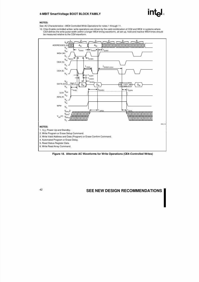
8/12/2019 Intel 4-Mbit SmartVolt device Guide
http://slidepdf.com/reader/full/intel-4-mbit-smartvolt-device-guide 42/57
4-MBIT SmartVoltage BOOT BLOCK FAMILY E
42 SEE NEW DESIGN RECOMMENDATIONS
NOTES:
See AC Characteristics —WE# Controlled Write Operations for notes 1 through 11.
12. Chip-Enable controlled writes: write operations are driven by the valid combination of CE# and WE# in systems whereCE# defines the write pulse-width (within a longer WE# timing waveform), all set-up, hold and inactive WE# times shouldbe measured relative to the CE# waveform.
ADDRESSES (A)
WE# (W)
OE# (G)
CE# (E)
DATA (D/Q)
RP# (P)
IHV
ILV
IHV
ILV
IHV
ILV
IHV
ILV
HHV6.5V
ILV
IND
INA INA
AVAVt
ValidSRDIND
QVPHtPHHEHt
High Z EHDXt
IHV
IL
V
V (V)PP
1 2 3 4 65
EHAXt
EHQV1,2,3,4tEHELt
EHWHt
ELEHt
DVEHt
VPEHt QVVLt
PHELt
WLELt
AVEHt
PPLKVPPH
V 1
2PPHV
ILV
IHVILV
IHV
WP#
IND
0530_18
NOTES:
1. VCC Power-Up and Standby.
2. Write Program or Erase Setup Command.
3. Write Valid Address and Data (Program) or Erase Confirm Command.
4. Automated Program or Erase Delay.
5. Read Status Register Data.
6. Write Read Array Command.
Figure 18. Alternate AC Waveforms for Write Operations (CE# –Controlled Writes)

8/12/2019 Intel 4-Mbit SmartVolt device Guide
http://slidepdf.com/reader/full/intel-4-mbit-smartvolt-device-guide 43/57
E 4-MBIT SmartVoltage BOOT BLOCK FAMILY
43SEE NEW DESIGN RECOMMENDATIONS
4.8 Erase and Program Timings —CommercialTA = 0 °C to +70 °C
VPP 5 V ± 10% 12 V ± 5%
VCC 3.3 ± 0.3 V 5 V ± 10% 3.3 ± 0.3 V 5 V ± 10%
Parameter Typ Max Typ Max Typ Max Typ Max Unit
Boot/Parameter Block Erase Time 0.84 7 0.8 7 0.44 7 0.34 7 s
Main Block Erase Time 2.4 14 1.9 14 1.3 14 1.1 14 s
Main Block Program Time (Byte) 1.7 1.8 1.6 1.2 s
Main Block Program Time (Word) 1.1 0.9 0.8 0.6 s
Byte Program Time(4) 10 10 8 8 µs
Word Program Time(4) 13 13 8 8 µs
NOTES:
1. All numbers are sampled, not 100% tested.
2. Max erase times are specified under worst case conditions. The max erase times are tested at the same valueindependent of VCC and VPP. See Note 3 for typical conditions.
3. Typical condi tions are +25 °C with VCC and VPP at the center of the specified voltage range. Production programming usingVCC = 5.0 V, VPP = 12.0 V typically results in a 60% reduction in programming time.
4. Contact your Intel field representative for more information.
4.9 Extended Operating Conditions
Table 11. Extended Temperature and VCC Operating Conditions
Symbol Parameter Notes Min Max Units
TA Operating Temperature –40 +85 °C
VCC 2.7 V–3.6 V VCC Supply Voltage 1 2.7 3.6 Volts
3.3 V VCC Supply Voltage (± 0.3 V) 1 3.0 3.6 Volts
5 V VCC Supply Voltage (10%) 2 4.50 5.50 Volts
NOTES:
1. AC specifications are valid at both voltage ranges. See DC Characteristics tables for voltage range-specific specifications.2. 10% VCC specifications apply to 80 ns and 120 ns versions in their standard test configuration.

8/12/2019 Intel 4-Mbit SmartVolt device Guide
http://slidepdf.com/reader/full/intel-4-mbit-smartvolt-device-guide 44/57

8/12/2019 Intel 4-Mbit SmartVolt device Guide
http://slidepdf.com/reader/full/intel-4-mbit-smartvolt-device-guide 45/57
E 4-MBIT SmartVoltage BOOT BLOCK FAMILY
45SEE NEW DESIGN RECOMMENDATIONS
4.11 DC Characteristics —Extended Temperature Operations
Prod TBE-120 TBV-80 TBV-80
TBE-120
Sym Parameter VCC 2.7 V –3.6 V 3.3 ± 0.3 V 5 V ± 10% Unit Test Conditions
Notes Typ Max Typ Max Typ Max
IIL Input LoadCurrent
1 ± 1.0 ± 1.0 ± 1.0 µA VCC = VCCMaxVIN = VCC or GND
ILO Output
Leakage
Current
1 ± 10 ± 10 ± 10 µA VCC = VCC Max
VIN = VCC or GND
ICCSVCC
Standby
Current
1,3 50 110 60 110 70 150 µA CMOS LevelsVCC = VCC Max
CE# = RP# = WP# =VCC ± 0.2 V
0.4 1.5 0.4 1.5 0.8 2.5 mA TTL LevelsVCC = VCC Max
CE# = RP# = BYTE#= VIH
ICCDVCC Deep
Power-
Down
Current
1 0.2 8 0.2 8 0.2 8 µA VCC = VCC Max
VIN = VCC or GND
RP# = GND ± 0.2 V
ICCRVCC Read
Current for
Word or
Byte
1,5,6 14 30 15 30 50 65 mA CMOS INPUTS
VCC = VCC Max
CE = VIL
f = 10 MHz (5 V)
5 MHz (3.3 V)
IOUT = 0 mA
Inputs = GND ± 0.2 V
or VCC ± 0.2 V
14 30 15 30 55 70 mA TTL INPUTS
VCC = VCC MaxCE# = VIL
f = 10 MHz (5 V),
5 MHz (3.3 V)
IOUT = 0 mA
Inputs = VIL or VIH

8/12/2019 Intel 4-Mbit SmartVolt device Guide
http://slidepdf.com/reader/full/intel-4-mbit-smartvolt-device-guide 46/57

8/12/2019 Intel 4-Mbit SmartVolt device Guide
http://slidepdf.com/reader/full/intel-4-mbit-smartvolt-device-guide 47/57

8/12/2019 Intel 4-Mbit SmartVolt device Guide
http://slidepdf.com/reader/full/intel-4-mbit-smartvolt-device-guide 48/57
4-MBIT SmartVoltage BOOT BLOCK FAMILY E
48 SEE NEW DESIGN RECOMMENDATIONS
4.11 DC Characteristics —Extended Temperature Operations (Continued)
Prod TBE-120 TBV-80 TBV-80TBE-120
Sym Parameter VCC 2.7 V –3.6 V 3.3 ± 0.3 V 5 V ± 10% Unit Test Conditions
Notes Min Max Min Max Min Max
VID
A9
Intelligent
Identifier
Voltage
11.4 12.6 11.4 12.6 11.4 12.6 V
VIL Input Low
Voltage
–0.5 0.8 –0.5 0.8 –0.5 0.8 V
VIH Input High
Voltage
2.0 VCC
±
0.5V
2.0 VCC
±
0.5V
2.0 VCC
±
0.5V
V
VOL Output Low
Voltage
0.45 0.45 0.45 V VCC = VCC Min
IOL = 5.8 mA (5 V)
2 mA (3.3 V)
VPP = 12 V
VOH1 Output
HighVoltage
(TTL)
2.4 2.4 2.4 V VCC = VCC Min
IOH
= –2.5 mA
VOH2 Output
High
Voltage
0.85
×VCC
0.85
×VCC
0.85
×VCC
V VCC = VCC Min
IOH = –2.5 mA
(CMOS) VCC –
0.4V
VCC –
0.4V
VCC –
0.4V
V VCC = VCC Min
IOH = –100 µA
VPPLKVPP
Lock-Out
Voltage
3 0.0 1.5 0.0 1.5 0.0 1.5 V Complete Write
Protection
VPPH1 VPP during
Prog/Erase4.5 5.5 4.5 5.5 4.5 5.5 V VPP at 5 V
VPPH2 Operations 11.4 12.6 11.4 12.6 11.4 12.6 V VPP at 12 V
VLKOVCC
Erase/Write
Lock
Voltage
8 2.0 2.0 2.0 V
VHH RP#
Unlock
Voltage
11.4 12.6 11.4 12.6 11.4 12.6 V VPP = 12 V
Boot Block Write/ Erase

8/12/2019 Intel 4-Mbit SmartVolt device Guide
http://slidepdf.com/reader/full/intel-4-mbit-smartvolt-device-guide 49/57
E 4-MBIT SmartVoltage BOOT BLOCK FAMILY
49SEE NEW DESIGN RECOMMENDATIONS
NOTES:
1. All currents are in RMS unless otherwise noted. Typical values at VCC = 5.0 V, T = +25 °C. These currents are valid for allproduct versions (packages and speeds).
2. ICCES is specified with device de-selected. If device is read while in erase suspend, current draw is sum of ICCES and ICCR.
3. Block erases and word/byte programs inhibited when VPP = VPPLK, and not guaranteed in the range between VPPH1 andVPPLK.
4. Sampled, not 100% tested.
5. Automatic Power Savings (APS) reduces ICCR to less than 1 mA typical, in static operation.
6. CMOS Inputs are either VCC ± 0.2 V or GND ± 0.2 V. TTL Inputs are either VIL or VIH.
7. For the 28F004B address pin A10 follows the COUT capacitance numbers.
8. For all BV/CV/BE/CE parts, VLKO = 2.0 V for 2.7 V, 3.3 V and 5.0 V operations.

8/12/2019 Intel 4-Mbit SmartVolt device Guide
http://slidepdf.com/reader/full/intel-4-mbit-smartvolt-device-guide 50/57

8/12/2019 Intel 4-Mbit SmartVolt device Guide
http://slidepdf.com/reader/full/intel-4-mbit-smartvolt-device-guide 51/57
E 4-MBIT SmartVoltage BOOT BLOCK FAMILY
51SEE NEW DESIGN RECOMMENDATIONS
4.12 AC Characteristics —Read Only Operations(1) —Extended Temperature
Prod TBE-120 TBV-80 TBV-80
TBE-120
Sym Parameter VCC 2.7V –3.6V(5) 3.3 ±0.3V(5) 5V±10%(6) Unit
Load 50 pF 50 pF 100 pF
Notes Min Max Min Max Min Max
tAVAV Read Cycle Time 120 110 80 ns
tAVQV Address to Output Delay 120 110 80 ns
tELQV CE# to Output Delay 2 120 110 80 ns
tPHQV RP# to Output Delay 0.8 0.8 0.45 µs
tGLQV OE# to Output Delay 2 65 65 40 ns
tELQX CE# to Output in Low Z 3 0 0 0 ns
tEHQZ CE# to Output in High Z 3 25 25 20 ns
tGLQX OE# to Output in Low Z 3 0 0 0 ns
tGHQZ OE# to Output in High Z 3 25 25 20 ns
tOH Output Hold from Address, CE#,
or OE# Change, Whichever
Occurs First
3 0 0 0 ns
tELFL
tELFH
CE# Low to BYTE# High or Low 3 5 5 5 ns
tAVFL Address to BYTE# High or Low 3 0 0 0 ns
tFLQV
tFHQV
BYTE# to Output Delay 3,4 120 110 80 ns
tFLQZ BYTE# Low to Output in High Z 3 45 45 30 ns
tPLPH Reset Pulse Width Low 7 150 150 60 ns
tPLQZ RP# Low to Output High Z 150 150 60 ns
NOTES:
1. See AC Input/Output Reference Waveform for timing measurements.
2. OE# may be delayed up to tCE –tOE after the falling edge of CE# without impact on tCE.
3. Sampled, but not 100% tested.
4. tFLQV, BYTE# switching low to valid output delay will be equal to tAVQV, measured from the time DQ15 /A –1 becomes valid.
5. See Test Configuration (Figure 22), 2.7 V –3.6 V and 3.3 ± 0.3 V Standard Test component values.
6. See Test Configuration (Figure 22), 5 V Standard Test component values.
7. The specification tPLPH is the minimum time RP# must be held low to produce a valid reset of the device.
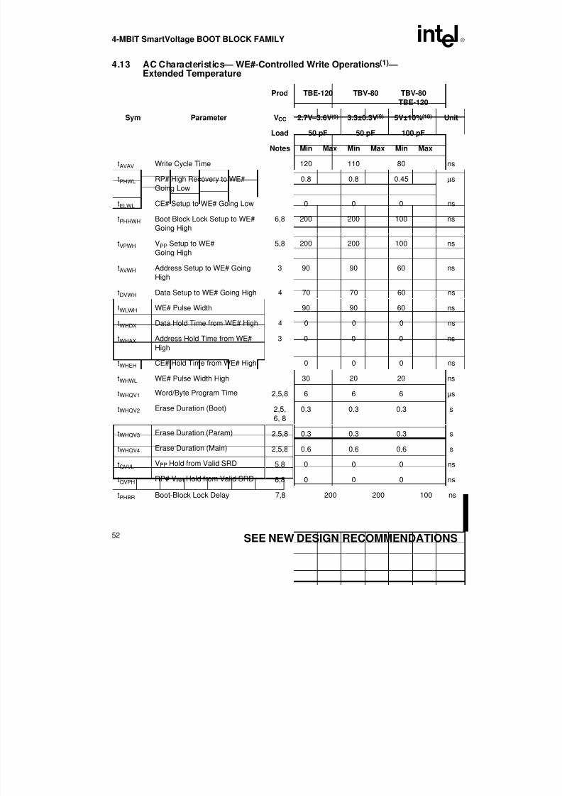
8/12/2019 Intel 4-Mbit SmartVolt device Guide
http://slidepdf.com/reader/full/intel-4-mbit-smartvolt-device-guide 52/57
4-MBIT SmartVoltage BOOT BLOCK FAMILY E
52 SEE NEW DESIGN RECOMMENDATIONS
4.13 AC Characteristics — WE#-Controlled Write Operations(1) —Extended Temperature
Prod TBE-120 TBV-80 TBV-80
TBE-120
Sym Parameter VCC 2.7V –3.6V(9) 3.3±0.3V(9) 5V±10%(10) Unit
Load 50 pF 50 pF 100 pF
Notes Min Max Min Max Min Max
tAVAV Write Cycle Time 120 110 80 ns
tPHWL RP# High Recovery to WE#
Going Low
0.8 0.8 0.45 µs
tELWL CE# Setup to WE# Going Low 0 0 0 ns
tPHHWH Boot Block Lock Setup to WE#
Going High
6,8 200 200 100 ns
tVPWH VPP Setup to WE#
Going High
5,8 200 200 100 ns
tAVWH Address Setup to WE# Going
High
3 90 90 60 ns
tDVWH Data Setup to WE# Going High 4 70 70 60 ns
tWLWH WE# Pulse Width 90 90 60 ns
tWHDX Data Hold Time from WE# High 4 0 0 0 ns
tWHAX Address Hold Time from WE#
High
3 0 0 0 ns
tWHEH CE# Hold Time from WE# High 0 0 0 ns
tWHWL WE# Pulse Width High 30 20 20 ns
tWHQV1 Word/Byte Program Time 2,5,8 6 6 6 µs
tWHQV2 Erase Duration (Boot) 2,5,
6, 8
0.3 0.3 0.3 s
tWHQV3 Erase Duration (Param) 2,5,8 0.3 0.3 0.3 s
tWHQV4 Erase Duration (Main) 2,5,8 0.6 0.6 0.6 s
tQVVLVPP Hold from Valid SRD 5,8 0 0 0 ns
tQVPHRP# VHH Hold from Valid SRD 6,8 0 0 0 ns
tPHBR Boot-Block Lock Delay 7,8 200 200 100 ns

8/12/2019 Intel 4-Mbit SmartVolt device Guide
http://slidepdf.com/reader/full/intel-4-mbit-smartvolt-device-guide 53/57
E 4-MBIT SmartVoltage BOOT BLOCK FAMILY
53SEE NEW DESIGN RECOMMENDATIONS
NOTES:
1. Read timing characteristics during program and erase operations are the same as during read-only operations. Refer to ACCharacteristics during read mode.
2. The on-chip WSM completely automates program/erase operations; program/erase algorithms are now controlled internallywhich includes verify and margining operations.
3. Refer to command definition table for valid AIN. (Table 7)
4. Refer to command definition table for valid DIN. (Table 7)
5. Program/erase durations are measured to valid SRD data (successful operation, SR.7 = 1)
6. For boot block program/erase, RP# should be held at VHH or WP# should be held at VIH until operation completes
successfully.
7. Time tPHBR is required for successful locking of the boot block.
8. Sampled, but not 100% tested.
9. See Test Configuration (Figure 22), 2.7 V –3.6 V and 3.3 ± 0.3 V Standard Test component values.
10. See Test Configuration (Figure 22), 5 V Standard Test component values.

8/12/2019 Intel 4-Mbit SmartVolt device Guide
http://slidepdf.com/reader/full/intel-4-mbit-smartvolt-device-guide 54/57
4-MBIT SmartVoltage BOOT BLOCK FAMILY E
54 SEE NEW DESIGN RECOMMENDATIONS
4.14 AC Characteristics —CE#-Controlled Write Operations(1, 11) —ExtendedTemperature
Prod TBE-120 TBV-80 TBV-80
TBE-120
Sym Parameter VCC 2.7V –3.6V(9) 3.3 ±0.3V(9) 5V±10%(10) Unit
Load 50 pF 50 pF 100 pF
Notes Min Max Min Max Min Max
tAVAV Write Cycle Time 120 110 80 ns
tPHEL RP# High Recovery to CE#
Going Low
0.8 0.8 0.45 µs
tWLEL WE# Setup to CE# Going Low 0 0 0 ns
tPHHEH Boot Block Lock Setup to CE#
Going High
6,8 200 200 100 ns
tVPEH VPP Setup to CE# Going High 5,8 200 200 100 ns
tAVEH Address Setup to CE# Going
High
90 90 60 ns
tDVEH Data Setup to CE# Going High 3 70 70 60 ns
tELEH CE# Pulse Width 4 90 90 60 ns
tEHDX Data Hold Time from CE# High 0 0 0 ns
tEHAX Address Hold Time from CE#
High
4 0 0 0 ns
tEHWH WE# Hold Time from CE# High 3 0 0 0 ns
tEHEL CE# Pulse Width High 20 20 20 ns
tEHQV1 Word/Byte Program Time 2,5 6 6 6 µs
tEHQV2 Erase Duration (Boot) 2,5,6 0.3 0.3 0.3 s
tEHQV3 Erase Duration (Param) 2,5 0.3 0.3 0.3 s
tEHQV4 Erase Duration (Main) 2,5 0.6 0.6 0.6 s
tQVVL VPP Hold from Valid SRD 5,8 0 0 0 ns
tQVPH RP# VHH Hold from Valid SRD 6,8 0 0 0 ns
tPHBR Boot-Block Lock Delay 7,8 200 200 100 ns
NOTES:
See WE# Controlled Write Operations for notes 1 through 10.
11. Chip-Enable controlled writes: write operations are driven by the valid combination of CE# and WE# in systems where CE#defines the write pulse-width (within a longer WE# timing waveform), all set-up, hold and inactive WE# times should bemeasured relative to the CE# waveform.

8/12/2019 Intel 4-Mbit SmartVolt device Guide
http://slidepdf.com/reader/full/intel-4-mbit-smartvolt-device-guide 55/57
E 4-MBIT SmartVoltage BOOT BLOCK FAMILY
55SEE NEW DESIGN RECOMMENDATIONS
4.15 Erase and Program Timings —Extended TemperatureTA = –40 °C to +85 °C
VPP 5 V ± 10% 12 V ± 5%
VCC 2.7 V–3.6 V 3.3 ± 0.3 V 5 V ± 10% 2.7 V–3.6 V 3.3 ± 0.3 V 5 V ± 10%
Parameter Typ Max Typ Max Typ Max Typ Max Typ Max Typ Max Unit
Boot/ParameterBlock Erase Time
0.88 7 0.84 7 0.8 7 0.46 7 0.44 7 0.34 7 s
Main Block
Erase Time
2.5 14 2.4 14 1.9 14 1.36 14 1.3 14 1.1 14 s
Main Block
Program Time
(Byte Mode)
1.87 1.7 1.4 1.76 1.6 1.2 s
Main Block
Program Time
(Word Mode)
1.21 1.1 0.9 0.88 0.8 0.6 s
Byte Program
Time(4)
11 10 10 8.8 8 8 µs
Word ProgramTime(4)
14.3 13 13 8.8 8 8 µs
NOTES:
1. All numbers are sampled, not 100% tested.
2. Max erase times are specified under worst case conditions. The max erase times are tested at the same valueindependent of VCC and VPP. See Note 3 for typical conditions.
3. Typical condi tions are +25 °C with VCC and VPP at the center of the specified voltage range. Production programming usingVCC = 5.0 V, VPP = 12.0 V typically results in a 60% reduction in programming time.
4. Contact your Intel field representative for more information.

8/12/2019 Intel 4-Mbit SmartVolt device Guide
http://slidepdf.com/reader/full/intel-4-mbit-smartvolt-device-guide 56/57

8/12/2019 Intel 4-Mbit SmartVolt device Guide
http://slidepdf.com/reader/full/intel-4-mbit-smartvolt-device-guide 57/57