Intel 31244 PCI-X to Serial ATA Controller Developer’s Manual Sheets/Intel PDFs/31244.pdf ·...
252
Intel ® 31244 PCI-X to Serial ATA Controller Developer’s Manual April 2004 Order Number: 273603-006
Transcript of Intel 31244 PCI-X to Serial ATA Controller Developer’s Manual Sheets/Intel PDFs/31244.pdf ·...

Intel® 31244 PCI-X to Serial ATA ControllerDeveloper’s Manual
April 2004
Order Number: 273603-006

2 April 2004 Developer’s Manual
Intel® 31244 PCI-X to Serial ATA Controller
INFORMATION IN THIS DOCUMENT IS PROVIDED IN CONNECTION WITH INTELR PRODUCTS. EXCEPT AS PROVIDED IN INTEL’S TERMS AND CONDITIONS OF SALE FOR SUCH PRODUCTS, INTEL ASSUMES NO LIABILITY WHATSOEVER, AND INTEL DISCLAIMS ANY EXPRESS OR IMPLIED WARRANTY RELATING TO SALE AND/OR USE OF INTEL PRODUCTS, INCLUDING LIABILITY OR WARRANTIES RELATING TO FITNESS FOR A PARTICULAR PURPOSE, MERCHANTABILITY, OR INFRINGEMENT OF ANY PATENT, COPYRIGHT, OR OTHER INTELLECTUAL PROPERTY RIGHT.
Intel Corporation may have patents or pending patent applications, trademarks, copyrights, or other intellectual property rights that relate to the presented subject matter. The furnishing of documents and other materials and information does not provide any license, express or implied, by estoppel or otherwise, to any such patents, trademarks, copyrights, or other intellectual property rights.
Intel products are not intended for use in medical, life saving, life sustaining, critical control or safety systems, or in nuclear facility applications.
Intel may make changes to specifications and product descriptions at any time, without notice.
Designers must not rely on the absence or characteristics of any features or instructions marked “reserved” or “undefined.” Intel reserves these for future definition and shall have no responsibility whatsoever for conflicts or incompatibilities arising from future changes to them.
The Intel® 31244 PCI-X to Serial ATA Controller may contain design defects or errors known as errata which may cause the product to deviate from published specifications. Current characterized errata are available on request.
Contact your local Intel sales office or your distributor to obtain the latest specifications and before placing your product order.
Copies of documents which have an ordering number and are referenced in this document, or other Intel literature may be obtained by calling 1-800-548-4725 or by visiting Intel's website at http://www.intel.com.
AnyPoint, AppChoice, BoardWatch, BunnyPeople, CablePort, Celeron, Chips, CT Media, Dialogic, DM3, EtherExpress, ETOX, FlashFile, i386, i486, i960, iCOMP, InstantIP, Intel, Intel Centrino, Intel logo, Intel386, Intel486, Intel740, IntelDX2, IntelDX4, IntelSX2, Intel Create & Share, Intel GigaBlade, Intel InBusiness, Intel Inside, Intel Inside logo, Intel NetBurst, Intel NetMerge, Intel NetStructure, Intel Play, Intel Play logo, Intel SingleDriver, Intel SpeedStep, Intel StrataFlash, Intel TeamStation, Intel Xeon, Intel XScale, IPLink, Itanium, MCS, MMX, MMX logo, Optimizer logo, OverDrive, Paragon, PC Dads, PC Parents, PDCharm, Pentium, Pentium II Xeon, Pentium III Xeon, Performance at Your Command, RemoteExpress, SmartDie, Solutions960, Sound Mark, StorageExpress, The Computer Inside., The Journey Inside, TokenExpress, VoiceBrick, VTune, and Xircom are trademarks or registered trademarks of Intel Corporation or its subsidiaries in the United States and other countries.
*Other names and brands may be claimed as the property of others.
Copyright © 2004, Intel Corporation
Developer’s Manual April 2004 3
Intel® 31244 PCI-X to Serial ATA Controller
Contents1 About This Document ....................................................................................................................15
1.1 Reference Documents ........................................................................................................151.2 Terminology and Conventions ............................................................................................16
1.2.1 Representing Numbers ..........................................................................................161.2.2 Fields .....................................................................................................................161.2.3 Specifying Bit and Signal Values ...........................................................................171.2.4 Signal Name Conventions .....................................................................................171.2.5 Terminology ...........................................................................................................18
2 Overview........................................................................................................................................21
2.1 Features..............................................................................................................................222.2 PCI-X Interface ...................................................................................................................222.3 PCI Commands Supported in M/S (PCI IDE) Mode ...........................................................23
2.3.1 PCI Commands Supported in DPA Mode..............................................................242.4 Serial ATA Interface............................................................................................................252.5 Modes of Operation ............................................................................................................27
2.5.1 Master/Slave Mode (or PCI IDE Mode) .................................................................272.5.2 Direct Port Access Mode .......................................................................................272.5.3 Selecting DPA or M/S Mode ..................................................................................282.5.4 DPA Mode Port Initialization ..................................................................................28
2.6 Serial EEPROM Interface ...................................................................................................292.7 Extended Voltage Mode .....................................................................................................292.8 ACTIVITY LEDS .................................................................................................................30
2.8.1 Reference Clock Generation .................................................................................312.9 High-End Storage Features ................................................................................................312.10 JTAG Interface....................................................................................................................31
3 Serial EEPROM.............................................................................................................................32
3.1 Write Status Register (WRSR) Command..........................................................................343.1.1 PROGRAM Command...........................................................................................353.1.2 READ Command ...................................................................................................363.1.3 Write Disable (WRDI) Command...........................................................................373.1.4 Read Status Register (RDSR) Command..............................................................383.1.5 Write Enable (WREN) Command ..........................................................................393.1.6 Sector Erase (SECT_ERASE) Command .............................................................403.1.7 CHIP_ERASE Command ......................................................................................413.1.8 Read ID Register (RDID) Command......................................................................423.1.9 Serial EEPROM SPI Interface – Address 90h .......................................................43
3.1.9.1 Programming Details .............................................................................433.1.9.2 SPI Command / Control / Status Register - Address 90h ......................45
3.1.9.2.1 SPI Command.................................................................................453.1.9.2.2 SPI Control ......................................................................................453.1.9.2.3 SPI Status .......................................................................................45
3.1.9.3 SPI Data Register - Address 94h ...........................................................463.1.10 Detection of the EEPROM at Power-Up ................................................................46

4 April 2004 Developer’s Manual
Intel® 31244 PCI-X to Serial ATA Controller
4 Functional Blocks .......................................................................................................................... 48
4.1 Serial ATA........................................................................................................................... 484.1.1 Out-of-Band Signaling ........................................................................................... 50
4.2 Operational Blocks.............................................................................................................. 534.2.1 Serial Engine ......................................................................................................... 544.2.2 Register Interface .................................................................................................. 544.2.3 DMA Controller ...................................................................................................... 55
4.2.3.1 DMA Operation ...................................................................................... 574.2.3.2 Data Synchronization............................................................................. 584.2.3.3 DMA Error Conditions ............................................................................ 594.2.3.4 DMA Throughput.................................................................................... 60
4.2.4 Programmed I/O (PIO)........................................................................................... 624.2.5 Serial ATA II Native Command Queuing ...............................................................63
4.2.5.1 Race-free Status Return Mechanism..................................................... 644.2.5.2 Interrupt Aggregation ............................................................................. 644.2.5.3 First Party DMA (FPDMA)......................................................................65
5 Programming Interface.................................................................................................................. 66
5.1 PCI IDE Mode..................................................................................................................... 675.1.1 Native-PCI Mode ................................................................................................... 67
5.2 Direct Port Access Mode .................................................................................................... 695.2.1 Common Serial ATA Port Registers ......................................................................705.2.2 Command Block Registers .................................................................................... 705.2.3 Control Block Registers .........................................................................................715.2.4 DMA Controller Registers ...................................................................................... 715.2.5 SATA Superset Registers...................................................................................... 72
5.3 ATA Command Processing ................................................................................................ 745.3.1 LBA Addressing in PCI IDE Mode ......................................................................... 755.3.2 LBA Addressing in DPA Mode............................................................................... 76
5.4 Reset Initialization............................................................................................................... 775.5 Serial ATA BIST.................................................................................................................. 79
5.5.1 Loopback Mode Testing ........................................................................................ 815.5.2 Transmit-Only Mode Testing ................................................................................. 82
5.6 PCI Bus Error Conditions.................................................................................................... 835.6.1 Address and Attribute Parity Errors on the PCI Interface ...................................... 835.6.2 Data Parity Errors on the PCI Interface ................................................................. 84
5.6.2.1 Outbound Read Request Data Parity Errors..........................................845.6.2.1.1 Immediate Data Transfer ................................................................ 845.6.2.1.2 Split Response Termination ............................................................ 85
5.6.2.2 Outbound Write Request Data Parity Errors..........................................865.6.2.2.1 Outbound Writes that are Not MSI (Message Signaled Interrupts). 865.6.2.2.2 MSI Outbound Writes......................................................................86
5.6.2.3 Inbound Read Request Data Parity Errors ............................................875.6.2.3.1 Immediate Data Transfer ................................................................ 87
5.6.2.4 Inbound Write Request Data Parity Errors............................................. 875.6.2.5 Outbound Read Completion Data Parity Errors.....................................875.6.2.6 Split Completion Messages ................................................................... 88
5.6.3 Master Aborts on the PCI Interface ....................................................................... 895.6.3.1 Master-Aborts Signaled by Intel® 31244 PCI-X to Serial ATA Controller
as an Initiator .........................................................................................895.6.3.1.1 Master Aborts for Outbound Read or Write Request ...................... 89
Developer’s Manual April 2004 5
Intel® 31244 PCI-X to Serial ATA Controller
5.6.3.2 Master-Aborts Signaled by Intel® 31244 PCI-X to Serial ATA Controlleras a Target .............................................................................................90
5.6.3.2.1 Unsupported PCI Commands .........................................................905.6.3.2.2 PCI IDE Control Block Registers.....................................................90
5.6.4 Target Aborts on the PCI Interface ........................................................................915.6.4.1 Target Aborts for Outbound Read Request or Outbound
Write Request ........................................................................................915.6.4.2 Target-Aborts Signaled by Intel® 31244 PCI-X to Serial ATA Controller
as a Target .............................................................................................925.6.4.2.1 Configuration Read and Write.........................................................925.6.4.2.2 I/O Read and Write .........................................................................925.6.4.2.3 Memory Read..................................................................................92
5.6.5 Corrupted or Unexpected Split Completions..........................................................935.6.5.1 Completer Address ................................................................................935.6.5.2 Completer Attributes ..............................................................................93
5.6.6 SERR# Assertion and Detection............................................................................945.6.7 PCI Error Summary ...............................................................................................95
5.7 Serial ATA Bus and Device Error Conditions .....................................................................985.7.1 Serial ATA Device Error Conditions.......................................................................985.7.2 Serial ATA Bus and Protocol Error Conditions ......................................................98
5.8 SATA Port Interrupt Generation........................................................................................1005.9 Message-Signaled Interrupts ............................................................................................102
5.9.1 Level-Triggered Versus Edge-Triggered Interrupts .............................................1025.10 Register Definitions...........................................................................................................103
5.10.1 PCI IDE Mode Registers......................................................................................1035.10.2 PCI Configuration Registers ................................................................................109
5.10.2.1 SU Vendor ID Register - SUVID ..........................................................1095.10.2.2 SU Device ID Register - SUDID...........................................................1105.10.2.3 SU Command Register - SUCMD........................................................1115.10.2.4 SU Status Register - SUSR .................................................................1125.10.2.5 SU Revision ID Register - SURID........................................................1135.10.2.6 SU Class Code Register - SUCCR ......................................................1145.10.2.7 SU Cacheline Size Register - SUCLSR...............................................1155.10.2.8 SU Latency Timer Register - SULT .....................................................1165.10.2.9 SU Header Type Register - SUHTR ....................................................1175.10.2.10 SU BIST Register - SUBISTR..............................................................1185.10.2.11 SU Base Address Register 0 - SUBAR0..............................................1195.10.2.12 SU Base Address Register 1 - SUBAR1..............................................1205.10.2.13 SU Base Address Register 2 - SUBAR2..............................................1215.10.2.14 SU Base Address Register 3 - SUBAR3..............................................1225.10.2.15 SU Base Address Register 4 - SUBAR4..............................................1235.10.2.16 SU Base Address Register 5 - SUBAR5..............................................1245.10.2.17 SU Subsystem Vendor ID Register - SUSVIR .....................................1255.10.2.18 SU Subsystem ID Register - SUSIR ....................................................1265.10.2.19 SU Expansion ROM Base Address Register - SUEXROMBAR ..........1275.10.2.20 SU Capabilities Pointer Register - SU_Cap_Ptr ..................................1285.10.2.21 SU Expansion ROM Base Address - SUEXROM ................................1295.10.2.22 SU Interrupt Line Register - SUILR......................................................1305.10.2.23 SU Interrupt Pin Register - SUIPR.......................................................1315.10.2.24 SU Minimum Grant Register - SUMGNT .............................................1325.10.2.25 SU Maximum Latency Register - SUMLAT..........................................1335.10.2.26 SPI Command Register - SPICMDR ...................................................1345.10.2.27 SPI Control Register - SPICNTR .........................................................135

6 April 2004 Developer’s Manual
Intel® 31244 PCI-X to Serial ATA Controller
5.10.2.28 SPI Status Register - SPISTATR......................................................... 1365.10.2.29 SPI Data Register - SPIDATR .............................................................1375.10.2.30 SU Extended Control and Status Register 0 - SUECSR0 ................... 1385.10.2.31 SU DMA Control Status Register- SUDCSCR..................................... 1395.10.2.32 SU Dummy Register SUDR................................................................. 1405.10.2.33 SU Interrupt Status Register SUISR .................................................... 1415.10.2.34 SU Interrupt Mask Register SUIMR..................................................... 1425.10.2.35 SU Transaction Control SUTCR .......................................................... 1435.10.2.36 SU Target Split Completion Message Enable Register SUTSCMER ..1445.10.2.37 SU Target Delayed/Split Request Pending Register SUDRPR ........... 1455.10.2.38 SU Transaction Control 2 Register SUTC2R....................................... 1465.10.2.39 SU Master Deferred/Split Sequence Pending Register - SUMDSPR ..1485.10.2.40 SU Master Split Completion Message Received
with Error Message Register - SUMSCMREMR.................................. 1495.10.2.41 SU Arbiter Control - SUACR ................................................................ 1505.10.2.42 SU PCI-X Capability Identifier Register - SUPCI-X_Cap_ID ............... 1515.10.2.43 SU PCI-X Next Item Pointer Register - SUPCI-X_Next_Item_Ptr ....... 1525.10.2.44 SU PCI-X Command Register - SUPCIXCMD..................................... 1535.10.2.45 SU PCI-X Status Register - SUPCIXSR .............................................. 1545.10.2.46 SU PM Capability Identifier Register - SUPM_Cap_ID........................ 1565.10.2.47 SU PM Next Item Pointer Register - SUPM_Next_Item_Ptr ................1575.10.2.48 SU Power Management Capabilities Register - SUPMCR.................. 1585.10.2.49 SU Power Management Control/Status Register - SUPMCSR ........... 1595.10.2.50 SU MSI Capability Identifier Register - SUMSI_Cap_ID...................... 1605.10.2.51 SU MSI Next Item Pointer Register - SUMSI_Next_Ptr....................... 1615.10.2.52 SU MSI Message Control Register - SUMSI_Message_Control .........1625.10.2.53 SU MSI Message Address Register - SUMSI_Message_Address ...... 1635.10.2.54 SU MSI Message Upper Address Register -
SUMSI_Message_Upper_Address ......................................................1645.10.2.55 SU MSI Message Data Register- SUMSI_Message_Data .................. 165
5.10.3 SU PCI IDE Mode Command Block Registers .................................................... 1665.10.3.1 SU IDE Data Port Register - SUIDR .................................................... 1665.10.3.2 SU IDE Error Register - SUIER ........................................................... 1675.10.3.3 SU IDE Features Register - SUIFR ..................................................... 1685.10.3.4 SU IDE Sector Count Register - SUISCR............................................ 1695.10.3.5 SU IDE Sector Number Register - SUISNR......................................... 1705.10.3.6 SU IDE Cylinder Low Register - SUICLR ............................................ 1715.10.3.7 SU IDE Cylinder High Register - SUICHR ........................................... 1725.10.3.8 SU IDE Device/Head Register - SUIDR...............................................1735.10.3.9 SU IDE Status Register - SUISR ......................................................... 1745.10.3.10 SU IDE Command Register - SUICR................................................... 175
5.10.4 SU PCI IDE Mode Control Block Registers ......................................................... 1765.10.4.1 SU IDE Device Control Register - SUIDCR ......................................... 1765.10.4.2 SU IDE Alternate Status Register - SUIASR ....................................... 177
5.10.5 SU PCI IDE Mode DMA Registers....................................................................... 1785.10.5.1 SU IDE Channel 0 DMA Command Register - SUICDCR0 ................. 1785.10.5.2 SU IDE Channel 0 DMA Status Register - SUICDSR0........................ 1795.10.5.3 SU IDE Channel 0 DMA Descriptor Table
Pointer Register - SUICDDTPR0 ......................................................... 1805.10.5.4 SU IDE Channel 1 DMA Command Register - SUICDCR1 ................. 1815.10.5.5 SU IDE Channel 1 DMA Status Register - SUICDSR1........................ 1825.10.5.6 SU IDE Channel 1 DMA Descriptor Table
Pointer Register - SUICDDTPR1 ......................................................... 1835.10.6 SU PCI DPA Mode Registers .............................................................................. 184

Developer’s Manual April 2004 7
Intel® 31244 PCI-X to Serial ATA Controller
5.10.7 SU PCI DPA Mode Base Address Registers .......................................................1925.10.7.1 SU PCI DPA Base Address Register 0 - SUPDBAR0 .........................1925.10.7.2 SU PCI DPA Upper Base Address Register 0 - SUPDUBAR0............193
5.10.8 SU PCI DPA Mode Common SATA Port Registers.............................................1945.10.8.1 SU PCI DPA Interrupt Pending Register - SUPDIPR ..........................1945.10.8.2 SU PCI DPA Interrupt Mask Register - SUPDIMR ..............................200
5.10.9 SU PCI DPA Mode Command Block Registers ...................................................2035.10.9.1 SU PCI DPA Data Port Register - SUPDDR........................................2035.10.9.2 SU PCI DPA Error Register - SUPDER ...............................................2045.10.9.3 SU PCI DPA Features Register - SUPDFR .........................................2055.10.9.4 SU PCI DPA Sector Count Register - SUPDSCR ...............................2065.10.9.5 SU PCI DPA Sector Number Register - SUPDSNR ............................2075.10.9.6 SU PCI DPA Cylinder Low Register - SUPDCLR ................................2085.10.9.7 SU PCI DPA Cylinder High Register - SUPDCHR...............................2095.10.9.8 SU PCI DPA Device/Head Register - SUPDDR ..................................2105.10.9.9 SU PCI DPA Status Register - SUPDSR.............................................2115.10.9.10 SU PCI DPA Command Register - SUPDCR ......................................212
5.10.10 SU PCI DPA Mode Control Block Registers ........................................................2135.10.10.1 SU PCI DPA Alternate Status Register - SUPDASR ...........................2135.10.10.2 SU PCI DPA Device Control Register - SUPDDCTLR ........................214
5.10.11 SU PCI DPA Mode DMA Registers .....................................................................2155.10.11.1 SU PCI DPA Upper DMA Descriptor Table
Pointer Register - SUPDUDDTPR .......................................................2155.10.11.2 SU PCI DPA Upper DMA Data Pointer Register - SUPDUDDBPR .....2165.10.11.3 SU PCI DPA DMA Command Register - SUPDDCMDR .....................2175.10.11.4 SU PCI DPA DMA Status Register - SUPDDSR .................................2185.10.11.5 SU PCI DPA DMA Descriptor Table Pointer Register - SUPDDDTPR 219
5.10.12 SU PCI DPA Mode Superset Registers ...............................................................2205.10.12.1 SU PCI DPA SATA SStatus Register - SUPDSSSR ...........................2205.10.12.2 SU PCI DPA SATA SError Register - SUPDSSER .............................2225.10.12.3 SU PCI DPA SATA SControl Register - SUPDSSCR..........................2255.10.12.4 SU PCI DPA Set Device Bits Register - SUPDSDBR..........................2265.10.12.5 SU PCI DPA PHY Feature Register - SUPDPFR ................................2275.10.12.6 SU PCI DPA BIST FIS Control and Status Register - SUPDBFCSR ..2285.10.12.7 SU PCI DPA BIST Errors Register - SUPDBER..................................2315.10.12.8 SU PCI DPA BIST Frames Register - SUPDBFR................................2325.10.12.9 SU PCI DPA Host BIST Data Low Register - SUPDHBDLR ...............2335.10.12.10SU PCI DPA Host BIST Data High Register - SUPDHBDHR.............2345.10.12.11SU PCI DPA Device BIST Data Low Register - SUPDDBDLR...........2355.10.12.12SU PCI DPA Device BIST Data High Register - SUPDDBDHR .........2365.10.12.13SU PCI DPA Queuing Table Base Address Register
Low - SUPDQTBARL...........................................................................2375.10.12.14SU PCI DPA Queuing Table Base Address Register
High - SUPDQTBARH .........................................................................2385.10.12.15SU PCI DPA DMA Setup FIS Control and
Status Register - SUPDDSFCSR ........................................................2395.10.12.16SU PCI DPA Host DMA Buffer Identifier
Low Register - SUPDHDBILR..............................................................2405.10.12.17SU PCI DPA Host DMA Buffer Identifier
High Register - SUPDHDBIHR ............................................................2415.10.12.18SU PCI DPA Host Reserved DWORD Register 0 - SUPDHRDR0.....2425.10.12.19SU PCI DPA Host DMA Buffer Offset Register - SUPDHDBOR ........2435.10.12.20SU PCI DPA Host DMA Transfer Count Register - SUPDHDTCR .....2445.10.12.21SU PCI DPA Host Reserved DWORD Register 1- SUPDHRDR1......245

8 April 2004 Developer’s Manual
Intel® 31244 PCI-X to Serial ATA Controller
5.10.12.22SU PCI DPA Device DMA Buffer Identifier Low Register - SUPDDDBILR.............................................................. 246
5.10.12.23SU PCI DPA Device DMA Buffer Identifier High Register - SUPDDDBIHR ............................................................ 247
5.10.12.24SU PCI DPA Host Reserved DWORD Register 0 - SUPDHRDR0..... 2485.10.12.25SU PCI DPA Device DMA Buffer Offset Register - SUPDDDBOR..... 2495.10.12.26SU PCI DPA Device DMA Transfer Count Register - SUPDDDTCR .2505.10.12.27SU PCI DPA Device Reserved DWORD Register 1 - SUPDDRDR1 .251
Developer’s Manual April 2004 9
Intel® 31244 PCI-X to Serial ATA Controller
Figures1 Intel® 31244 PCI-X to Serial ATA Controller Block Diagram ......................................................212 Serial ATA Unit Block Diagram...................................................................................................263 Common LED and Serial EEPROM Options ..............................................................................304 Serial EEPROM Interface ...........................................................................................................325 Write Status Register (WRSR) Operation...................................................................................346 Write Memory (PROGRAM) Operation, 4 Byte ..........................................................................357 Read Memory (READ) Operation, 4 Byte...................................................................................368 Write Disable (WRDI) Operation.................................................................................................379 Read Status Register (RDSR) Operation ...................................................................................3810 Write Enable (WREN) Operation ................................................................................................3911 Sector Erase (SECT_ERASE) Operation ...................................................................................4012 Chip Erase (CHIP_ERASE) Operation .......................................................................................4113 Read ID Register (RDID) Operation ...........................................................................................4214 SATA Protocol Layers ................................................................................................................4915 Analog Front End (AFE) Cabling and OOB Signals ...................................................................5016 OOB Signals Timings .................................................................................................................5017 COMRESET Sequence ..............................................................................................................5118 COMINIT Sequence ...................................................................................................................5219 SATA Port Block Diagram ..........................................................................................................5320 DMA Descriptor Table ................................................................................................................5621 DMA Arbitration ..........................................................................................................................6022 SATA Unit Register Mapping in Native-PCI Mode......................................................................6823 SATA Unit Register Mapping in Direct Port Access Mode .........................................................6924 Common Serial ATA Port Registers ...........................................................................................7025 Command Block Registers for SATA Port 0 ...............................................................................7026 Control Block Registers for SATA Port 0 ....................................................................................7127 DMA Controller Registers for SATA Port 0.................................................................................7128 Far-End Retimed Loopback Setup .............................................................................................7929 Far-End Analog Loopback Setup................................................................................................8030 Near-End Analog Loopback Setup .............................................................................................8031 SATA Unit Interrupt Generation Block Diagram .......................................................................10132 SU in PCI IDE Mode Interface Configuration Header Format ..................................................10333 SATA Unit Interface Extended Configuration Header Format (PCI-X Capability) ....................10434 SU in PCI IDE Mode Interface Extended Configuration Header
Format (Power Management)...................................................................................................10435 SU in PCI IDE Mode Interface Extended Configuration Header Format (MSI Capability)........105

10 April 2004 Developer’s Manual
Intel® 31244 PCI-X to Serial ATA Controller
Tables1 Reference Documents................................................................................................................ 152 Terms and Definitions.................................................................................................................183 PCI Commands Supported in PCI IDE Mode............................................................................. 234 PCI Commands Supported in DPA Mode ..................................................................................245 DPA Mode Interface Features .................................................................................................... 276 BAR Register usage in M/S and DPA Modes............................................................................. 287 Normal Voltage Mode .................................................................................................................298 Extended Voltage Mode ............................................................................................................. 299 Serial EEPROM Interface Pins................................................................................................... 3310 SCLK Frequency ........................................................................................................................3311 Serial EEPROM Commands ...................................................................................................... 3312 Block Write Protect Bits .............................................................................................................. 3413 Byte Enables on ROM Memory Reads.......................................................................................3614 Status Register Format (Refer to Atmel* AT25F1024 Datasheet).............................................. 3815 Write and Read Command Types ..............................................................................................4416 PCI Byte Enables on Read and Write Operations ......................................................................4417 SPI Command ............................................................................................................................ 4518 SPI Control ................................................................................................................................. 4519 SPI Status................................................................................................................................... 4520 SPI Data Register - Address 94h ............................................................................................... 4621 Interrupt /Activity Status Combinations.......................................................................................5822 PCI-X Bus Efficiency for Reads.................................................................................................. 6023 PCI-X Bus Efficiency for Writes .................................................................................................. 6024 Read Transfer Rate on PCI-X Bus ............................................................................................. 6125 Write Transfer Rate on PCI-X Bus ............................................................................................. 6126 SATA Port Register Mapping in Native PCI IDE Mode .............................................................. 6727 SATA Superset Registers for SATA Port 0 in DPA Mode .......................................................... 7328 28-Bit LBA Address Bit Layout in PCI IDE Mode ....................................................................... 7529 48-Bit LBA Address Bit Layout ................................................................................................... 7530 48-Bit Address Loading Sequence ............................................................................................. 7531 28-Bit LBA Address Bit Layout in DPA Mode ............................................................................. 7632 48-Bit LBA Address Bit Layout in DPA Mode ............................................................................. 7633 31244 Controller Error Reporting Summary - PCI Interface ...................................................... 9534 31244 Controller Serial ATA Protocol and Bus Error Conditions ............................................... 9835 SATA Unit PCI Configuration Space Registers ........................................................................ 10638 SATA DMA Registers in PCI IDE Mode ................................................................................... 10836 SATA Command Block Registers in PCI IDE Mode................................................................. 10837 SATA Control Block Registers in PCI IDE Mode...................................................................... 10839 SU Vendor ID Register - SUVID............................................................................................... 10940 SU Device ID Register - SUDID ............................................................................................... 11041 SU Command Register - SUCMD ............................................................................................11142 SU Status Register - SUSR...................................................................................................... 11243 SU Revision ID Register - SURID ............................................................................................11344 SU Class Code Register - SUCCR........................................................................................... 11445 SU Cacheline Size Register - SUCLSR ................................................................................... 11546 SU Latency Timer Register - SULT .......................................................................................... 11647 SU Header Type Register - SUHTR......................................................................................... 11748 SU BIST Register - SUBISTR .................................................................................................. 11849 SU Base Address Register 0 - SUBAR0 .................................................................................. 119
Developer’s Manual April 2004 11
Intel® 31244 PCI-X to Serial ATA Controller
50 SU Base Address Register 1 - SUBAR1 ..................................................................................12051 SU Base Address Register 2 - SUBAR2 ..................................................................................12152 SU Base Address Register 3 - SUBAR3 ..................................................................................12253 SU Base Address Register 4 - SUBAR4 ..................................................................................12354 SU Base Address Register 5 - SUBAR5 ..................................................................................12455 SU Subsystem Vendor ID Register - SUSVIR..........................................................................12556 SU Subsystem ID Register - SUSIR.........................................................................................12657 SU Expansion ROM Base Address Register - SUEXROMBAR ...............................................12758 SU Capabilities Pointer Register - SU_Cap_Ptr .......................................................................12859 SU Expansion ROM Base Address - SUEXROM.....................................................................12960 SU Interrupt Line Register - SUILR ..........................................................................................13061 SU Interrupt Pin Register - SUIPR............................................................................................13162 SU Minimum Grant Register - SUMGNT ..................................................................................13263 SU Maximum Latency Register - SUMLAT ..............................................................................13364 SPI Command Register - SPICMDR ........................................................................................13465 SPI Control Register - SPICNTR ..............................................................................................13566 SPI Status Register - SPISTATR..............................................................................................13667 SPI Data Register - SPIDATR ..................................................................................................13768 SU Extended Control and Status Register 0 - SUECSR 0 .......................................................13869 SU DMA Control Status Register - SUDCSCR 0......................................................................13970 SU Dummy Register - SUDR....................................................................................................14071 SU Interrupt Status Register - SUISR.......................................................................................14172 SU Interrupt Mask Register - SUIMR........................................................................................14273 SU Transaction Control Register - SUTCR ..............................................................................14374 SU Target Split Completion Message Enable Register- SUTSCMER......................................14475 SU Target Split Completion Message Enable Register- SUTSCMER......................................14576 SU Transaction Control 2 Register- SUTC2R ..........................................................................14677 SU Master Split Completion Message Received with Error Message Register -
SUMSCMREMR .......................................................................................................................14878 SU Master Split Completion Message Received with Error Message Register -
SUMSCMREMR .......................................................................................................................14979 SU Arbiter Control Register SUACR.........................................................................................15080 SU PCI-X_Capability Identifier Register - SUPCI-X_Cap_ID ...................................................15181 SU PCI-X Next Item Pointer Register - SUPCI-X_Next_Item_Ptr ............................................15282 SU PCI-X Command Register - SUPCIXCMD .........................................................................15383 SU PCI-X Status Register - SUPCIXSR ...................................................................................15484 SU PM_Capability Identifier Register - SUPM_Cap_ID............................................................15685 SU PM Next Item Pointer Register - SUPM_Next_Item_Ptr.....................................................15786 SU Power Management Capabilities Register - SUPMCR.......................................................15887 SU Power Management Control/Status Register - SUPMCSR ................................................15988 SU MSI Capability Identifier Register - SUMSI_Cap_ID...........................................................16089 SU MSI Next Item Pointer Register - SUMSI_Next_Ptr............................................................16190 SU MSI Message Control Register - SUMSI_Message_Control ..............................................16291 SU MSI Message Address Register - SUMSI_Message_Address...........................................16392 SU MSI Message Upper Address Register - SUMSI_Message_Upper_Address ....................16493 SU MSI Message Data Register - SUMSI_Message_Data ......................................................16594 SU IDE Data Port Register - SUIDR.........................................................................................16695 SU IDE Error Register - SUIER ................................................................................................16796 SU IDE Features Register - SUIFR ..........................................................................................16897 SU IDE Sector Count Register - SUISCR.................................................................................169

12 April 2004 Developer’s Manual
Intel® 31244 PCI-X to Serial ATA Controller
98 SU IDE Sector Number Register - SUISNR ............................................................................. 17099 SU IDE Cylinder Low Register - SUICLR ................................................................................. 171100 SU IDE Cylinder High Register - SUICHR................................................................................172101 SU IDE Device/Head Register - SUIDHR................................................................................. 173102 SU IDE Status Register - SUISR.............................................................................................. 174103 SU IDE Command Register - SUICR .......................................................................................175104 SU IDE Device Control Register - SUIDCR.............................................................................. 176105 SU IDE Alternate Status Register - SUIASR ............................................................................ 177106 SU IDE Channel 0 DMA Command Register - SUICDCR0......................................................178107 SU IDE Channel 0 DMA Status Register - SUICDSR0 ............................................................ 179108 SU IDE Channel 0 DMA Descriptor Table Pointer Register - SUICDDTPR0........................... 180109 SU IDE Channel 1 DMA Command Register - SUICDCR1......................................................181110 SU IDE Channel 1 DMA Status Register - SUICDSR1 ............................................................ 182111 SU IDE Channel 1 DMA Descriptor Table Pointer Register - SUICDDTPR1........................... 183112 Configuration Space Comparison............................................................................................. 184113 SATA Port Registers Mapping in PCI DPA Mode ....................................................................185114 SU PCI DPA Base Address Register 0 - SUDBAR0 ................................................................ 192115 SU PCI DPA Upper Base Address Register 0 - SUPDUBAR0 ................................................ 193116 SU PCI DPA Interrupt Pending Register - SUPDIPR ............................................................... 194117 SU PCI DPA Interrupt Mask Register - SUPDIMR ................................................................... 200118 SU PCI DPA Data Port Register - SUPDDR ............................................................................ 203119 SU PCI DPA Error Register - SUPDER.................................................................................... 204120 SU PCI DPA Features Register - SUPDFR.............................................................................. 205121 SU PCI DPA Sector Count Register - SUPDSCR ....................................................................206122 SU PCI DPA Sector Number Register - SUPDSNR................................................................. 207123 SU PCI DPA Cylinder Low Register - SUPDCLR..................................................................... 208124 SU PCI DPA Cylinder High Register - SUPDCHR ................................................................... 209125 SU PCI DPA Device/Head Register - SUPDDHR ....................................................................210126 SU PCI DPA Status Register - SUPDSR ................................................................................. 211127 SU PCI DPA Command Register - SUPDCR........................................................................... 212128 SU PCI DPA Alternate Status Register - SUPDASR................................................................ 213129 SU PCI DPA Device Control Register - SUPDDCTLR .............................................................214130 SU PCI DPA Upper DMA Descriptor Table Pointer Register - SUPDUDDTPR ....................... 215131 SU PCI DPA Upper DMA Data Buffer Pointer Register - SUPDUDDPR ................................. 216132 SU PCI DPA DMA Command Register - SUPDDCMDR.......................................................... 217133 SU PCI DPA DMA Status Register - SUPDDSR...................................................................... 218134 SU PCI DPA DMA Descriptor Table Pointer Register - SUPDDDTPR .................................... 219135 SU PCI DPA SATA SStatus Register - SUPDSSSR................................................................ 220136 SU PCI DPA SATA SError Register - SUPDSSER ..................................................................222137 SU PCI DPA SATA SControl Register - SUPDSSCR .............................................................. 225138 SU PCI DPA Set Device Bits Register - SUPDSDBR .............................................................. 226139 SU PCI DPA PHY Feature Register - SUPDPFR..................................................................... 227140 SU PCI DPA BIST FIS Control and Status Register - SUPDBFCSR ....................................... 228141 SU PCI DPA BIST Errors Register - SUPDBER ...................................................................... 231142 SU PCI DPA BIST Frames Register - SUPDBFR ....................................................................232143 SU PCI DPA Host BIST Data Low Register - SUPDHBDLR.................................................... 233144 SU PCI DPA Host BIST Data High Register - SUPDHBDHR .................................................. 234145 SU PCI DPA Device BIST Data Low Register - SUPDDBDLR ................................................ 235146 SU PCI DPA Device BIST Data High Register - SUPDDBDHR...............................................236147 SU PCI DPA Device BIST Data High Register - SUPDDBDHR...............................................237

Developer’s Manual April 2004 13
Intel® 31244 PCI-X to Serial ATA Controller
148 SU PCI DPA Device BIST Data High Register - SUPDDBDHR ...............................................238149 SU PCI DPA DMA Setup FIS Control and Status Register - SUPDDSFCSR ..........................239150 SU PCI DPA Host DMA Buffer Identifier Low Register - SUPDHDBILR ..................................240151 SU PCI DPA Host DMA Buffer Identifier High Register - SUPDHDBIHR.................................241152 SU PCI DPA Host Reserved DWORD Register 0 - SUPDHRDR 0..........................................242153 SU PCI DPA Host DMA Buffer Offset Register - SUPDHDBOR ..............................................243154 SU PCI DPA Host DMA Transfer Count Register - SUPDHDTCR...........................................244155 SU PCI DPA Host Reserved DWORD Register 1- SUPDHRDR 1...........................................245156 SU PCI DPA Device DMA Buffer Identifier Low Register - SUPDDDBILR...............................246157 SU PCI DPA Device DMA Buffer Identifier High Register - SUPDDDBIHR .............................247158 SU PCI DPA Device Reserved DWORD Register 0 - SUPDDRDR0 .......................................248159 SU PCI DPA Device DMA Buffer Offset Register - SUPDDDBOR...........................................249160 SU PCI DPA Device DMA Transfer Count Register - SUPDDTCR..........................................250161 SU PCI DPA Device Reserved DWORD Register 1 - SUPDDRDR1 .......................................251
14 April 2004 Developer’s Manual
Intel® 31244 PCI-X to Serial ATA Controller
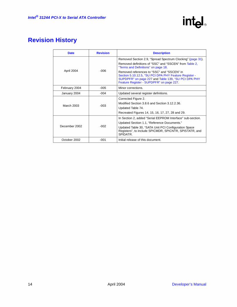
Revision History
Date Revision Description
April 2004 -006
Removed Section 2.9, “Spread Spectrum Clocking” (page 31).
Removed definitions of “SSC” and “SSCEN” from Table 2, “Terms and Definitions” on page 18.
Removed references to “SSC” and “SSCEN” in Section 5.10.12.5, “SU PCI DPA PHY Feature Register - SUPDPFR” on page 227 and Table 139, “SU PCI DPA PHY Feature Register - SUPDPFR” on page 227.
February 2004 -005 Minor corrections.
January 2004 -004 Updated several register definitions.
March 2003 -003
Corrected Figure 2.
Modified Section 3.8.6 and Section 3.12.2.36.
Updated Table 74.
Recreated Figures 14, 15, 16, 17, 27, 28 and 29.
December 2002 -002
In Section 2, added “Serial EEPROM Interface” sub-section.
Updated Section 1.1, “Reference Documents.”
Updated Table 30, “SATA Unit PCI Configuration Space Registers”, to include SPICMDR, SPICNTR, SPISTATR, and SPIDATR.
October 2002 -001 Initial release of this document.

Developer’s Manual April 2004 15
Intel® 31244 PCI-X to Serial ATA ControllerAbout This Document
About This Document 1
1.1 Reference Documents
Table 1. Reference Documents
Documentation Document Number/Source
Intel® 31244 PCI-X to Serial ATA Controller Datasheet 273595
Intel® 31244 PCI-X to Serial ATA Controller Design Guide 273651
Intel® 31244 PCI-X to Serial ATA Controller Red Canyon CRB Manual 273801
Atmel* Serial Memory Specification AT25F512/AT25F1024 http://www.atmel.fi/atmel/acrobat/doc1440.pdf
AT Attachment with Packet Interface-6 (ATA/ATAPI-6) Specification, ANSI/INCITS #361-2002
http://www.techstreet.com/cgi-bin/detail?product_id=932242
Serial ATA Specification http://www.serialata.org
Serial ATA II: Extensions to Serial ATA 1.0 Specification http://www.serialata.org/collateral/index.shtml
PCI Local Bus Specification, Revision 2.2 http://www.pcisig.com
PCI-X Addendum to the PCI Local Bus Specification, Revision 1.0a http://www.pcisig.com
PCI Bus Power Management Interface Specification, Revision 1.1 http://www.pcisig.com
PCI IDE Specification, Revision 1.0 http://www.bswd.com/pciide.pdf
STMicroelectronics* M25P10 Serial Flash Memory http://us.st.com/stonline/books/pdf/docs/7022.pdf

16 April 2004 Developer’s Manual
Intel® 31244 PCI-X to Serial ATA ControllerAbout This Document
1.2 Terminology and Conventions
1.2.1 Representing Numbers
All numbers in this document may be assumed to be Base10, unless designated otherwise. In text, numbers in Base16 are represented as ‘nnnH’, where the ‘H’ signifies hexadecimal. In pseudo code descriptions, hexadecimal numbers are represented in the form 0x1234 ABCD. Binary numbers are not explicitly identified, but are assumed when bit operations or bit ranges are used.
1.2.2 Fields
Reserved: Is a field that may be used by an implementation. When the initial value of a reserved field is supplied by software, this value must be zero. Software should not modify reserved fields or depend on any values in reserved fields.
Read/Write: May be written to a new value following initialization. This field may always be read to return the current value.
Read Only: May be read to return the current value. Writes to read only fields are treated as no-op operations and will not change the current value, nor result in an error condition.
Read/Clear: May also be read to return the current value. A write to a read/clear field with the data value of 0 will cause no change to the field. A write to a read/clear field with a data value of 1 will cause the field to be cleared (reset to the value of 0). For example, when a read/clear field has a value of F0H, and a data value of 55H is written, the resultant field will be A0H.
Read/Set: May also be read to return the current value. A write to a read/set field with the data value of 0 will cause no change to the field. A write to a read/set field with a data value of 1 will cause the field to be set (set to the value of 1). For example, when a read/set field has a value of F0H, and a data value of 55H is written, the resultant field will be F5H.
Writeonce/Readonly: May be written to a new value once following initialization. After the this write has occurred, the writeonce/readonly field will treat all subsequent writes as no-op operations and will not change the current value or result in an error condition. The field may always be read to return the current value.

Developer’s Manual April 2004 17
Intel® 31244 PCI-X to Serial ATA ControllerAbout This Document
1.2.3 Specifying Bit and Signal Values
The terms set and clear in this specification refer to bit values in register and data structures. When a bit is set, its value is 1; when the bit is clear, its value is 0. Likewise, setting a bit means giving it a value of 1 and clearing a bit means giving it a value of 0.
The terms assert and deassert refer to the logically active or inactive value of a signal or bit, respectively.
1.2.4 Signal Name Conventions
All signal names use the PCI signal name convention of using the ‘#’ symbol at the end of a signal name to indicate that the signal active state occurs when it is at a low voltage. The absence of the ‘#’ symbol indicates that the signal active state occurs when it is at a high voltage.

18 April 2004 Developer’s Manual
Intel® 31244 PCI-X to Serial ATA ControllerAbout This Document
1.2.5 Terminology
To aid the discussion of the GD31244 controller architecture, the following terminology is used:
Table 2. Terms and Definitions (Sheet 1 of 2)
Term Definition
BAR Base Address Register
BIST Built-In Self Test
CFG Configure
CRB Customer Reference Board
Differential Signalsignal is comprised of a positive conductor and a negative conductor. The
differential signal is the voltage on the positive conductor minus the voltage on the negative conductor (i.e., TX+ – TX-).
DMA Direct Memory Access
Downstream At or toward a PCI bus with a higher number (after configuration).
DPA Direct Port Access Refers to a mode that allows more efficient access to the GD31244 registers. See also PCI IDE.
DWORD 32-bit data word.
HBA Host Bus Adapter
Host processor: Processor located upstream from the GD31244 controller.
Inbound Transactions Transactions that are aimed at the GD31244 controller by an external bus master device.
ISIInter-symbol interference. Data-dependent deterministic jitter caused by the time propagated at different rates by the transmission media. This translates into high-frequency,data-dependent, jitter.
JEDEC Provides standards for the semiconductor industry.
Jitter Jitter is a high-frequency, semi-random displacement of a signal from its ideal location.
M/S Master/Slave. Refers to a legacy ATA mode that uses the traditional methods for accessing the ATA and the DMA registers (see also DPA).
BAR Base Address Register
MR Memory Read
MRL Memory Read Line
MRM Memory Read Multiple
MSI Message Signalled Interrupts
MW Memory Write
MWI Memory Write and Invalidate
Network The trace of a PCB that completes an electrical connection between two or more components.
Outbound Transactions Transactions that are initiated by the controller to another target device.
PATA Parallel ATA
PBGA Plastic Ball Grid Array
PERR# Parity error
PIO Programmed I/O

Developer’s Manual April 2004 19
Intel® 31244 PCI-X to Serial ATA ControllerAbout This Document
PLL Phase Lock Loop
PLL This block is used to synchronize an internal clocking reference so that the input high-speed data stream may be properly decoded
PRD Physical Region Description
Prepreg
Material used for the lamination process of manufacturing PCBs. It consists of a layer of epoxy material that i placed between two cores. This layer melts into epoxy layer of epoxy material that i placed between two cores. This layer melts into epoxy when heated and forms around adjacent traces.
QWORD 64-bit data word.
RDID Read Manufacturer and Product ID
RDSR Read Status Register
RX This is a receiver port contains the basic high-speed receiver electronics.
RX + / RX - Inbound high-speed differential signals connected to the serial ATA cable.
RxData
10b encoding Serially encoded 10b data attached to the high-speed serial differential line receiver. The 8B/10B encoding scheme transmits eight bits as a 10-bit code group. This encoding is used with Gigabit Ethernet, Fibre Channel and InfiniBand.
SATA Serial ATA
SECT Sector
SERR# SERR is the System Error Signal on the PCI bus.
SPI Serial Peripheral Interface. SPI is used to access the GD31244 EEPROM.
Stub Branch from a trunk terminating at the pad of an agent.
Termination CalibrationTerminate the high-speed serial cable. This block is used to synchronize an internal clocking reference so that the input high-speed data stream may be properly decoded.
TX This is a transmit port that contains the basic high-speed driver electronics.
TX + / TX - Outbound high-speed differential signals connected to the serial ATA cable.
TxData Serially encoded 10b data attached to the high-speed serial differential line driver.
Upstream At or toward a PCI bus with a lower number (after configuration).
WEN Write Enable
WPEN Write Protection Enable
WRDI Reset Write Enable Latch
WREN Write Enable
WRSR Write Status Register
Table 2. Terms and Definitions (Sheet 2 of 2)
Term Definition

20 April 2004 Developer’s Manual
Intel® 31244 PCI-X to Serial ATA ControllerAbout This Document
This Page Left Intentionally Blank

Developer’s Manual April 2004 21
Intel® 31244 PCI-X to Serial ATA ControllerOverview
Overview 2
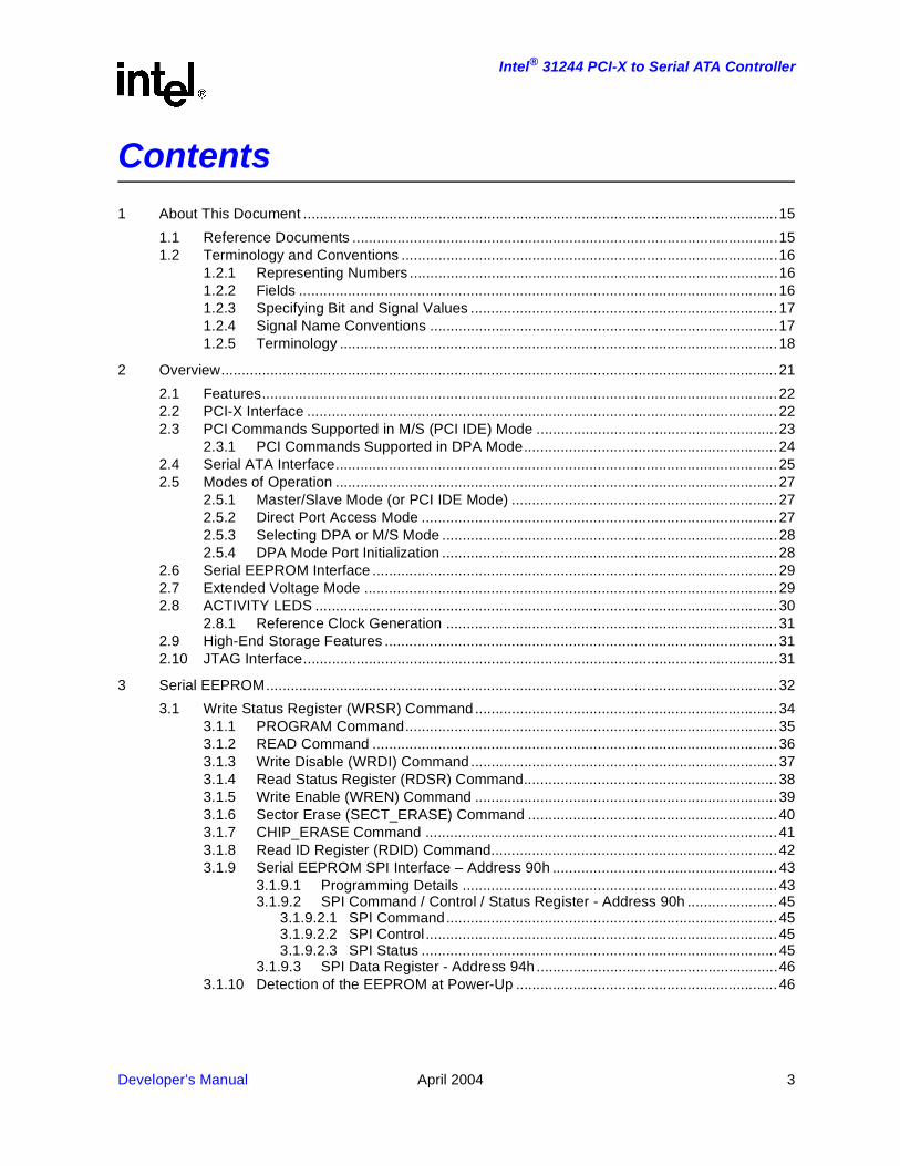
The Intel® 31244 PCI-X to Serial ATA Controller (GD31244) is a single-chip solution for a PCI-X to Serial ATA Controller. It accepts host commands through the PCI-X bus, processes them and transmits them to one of four Serial ATA targets. The GD31244 supports Serial ATA speeds of 1.5 Gbits/s of 8b/10b encoded data which is equivalent to 150 Mbytes/s of raw data. The GD31244 derives its Serial ATA clocks from an internal PLL with a reference clock of 37.5 MHz. On the 64-bit PCI-X bus, when run at the maximum frequency of 133 MHz, the GD31244 supports a maximum burst transfer rate of 1064 Mbytes/s.
The GD31244 controller may be used to build standalone PCI-X HBA cards to interface Serial ATA Disk Drives, CD-ROMs, DVD ROMs or Tape drives. The GD31244 is completely software compatible with all existing operating systems which support ATA interfaces: Windows*, Windows NT*, Linux*, Solaris*, Unix*, etc. In PC systems, the GD31244 may also be configured to provide additional storage capacity to systems already supporting four ATA targets. In non-PC systems, the GD31244 may be used as a generic storage controller in servers, RAID subsystems and Network Attached Storage (NAS) systems. The ease-of-use, flexibility, performance and low cost of the GD31244 make it an ideal choice for all of these applications.
In addition to PCI IDE mode, the GD31244 supports a new programming interface, referred to as Direct Port Access Mode. In this new mode, the SATA ports are set up to operate independently, for example no master/slave emulation is done as in PCI IDE mode. In this mode the SATA ports registers are memory-mapped.
Figure 1. Intel® 31244 PCI-X to Serial ATA Controller Block Diagram
B2843-01
OOB
Serializer
OOB
OOB
OOB
AD[63:0]SD0
SD1
SCLK
TX0P
CBE#[7:0]
PAR
PAR64
FRAME#
TRDY#
IRDY#
STOP#
DEVSEL#
REQ64#
ACK64#
REQ#
PERR#
SERR#
INTA#
GNT#
SCS#
TX0N
CLK
RST#
IDSEL
PCI-XInterface FIFO
and DMAEngine
EEPROM
Tran
sact
ion
Man
ager
Serial ATATransport/Link Layer
FIFOand DMAEngine
Serial ATATransport/Link Layer
FIFOand DMAEngine
Serial ATATransport/Link Layer
FIFOand DMAEngine
Serial ATATransport/Link Layer
DeserializerRX1NRX1P
SerializerTX1PTX1N
DeserializerRX1NRX1P
SerializerTX2PTX2N
DeserializerRX2NRX2P
SerializerTX3PTX3N
DeserializerRX3NRX3P
PH
Y In
terf
ace

22 April 2004 Developer’s Manual
Intel® 31244 PCI-X to Serial ATA ControllerOverview
2.1 Features
• Four SATA Ports at 1.5 Gbits/s
• Compliant with Serial ATA: High speed Serialized AT Attachment Specification, Revision 1.0e
• 64-bit/133MHz PCI-X Bus. Backwards compatible to PCI 32-bit/33 MHz and 64-bit/66 MHz
• Supports native PCI IDE
• Hot-Plug Drives
• Supports Master/Slave Mode for Compatibility with existing Operating Systems
• Supports SATA Direct Port Access
• Independent DMA Masters for each SATA Port
• 3.3V and 2.5V Supply, 2W maximum
2.2 PCI-X Interface
The 64-bit, 133 MHz PCI-X interface is fully compliant with the PCI Local Bus Specification, Revision 2.2 and the PCI-X Addendum to the Local Bus Specification, Revision 1.0. The PCI-X bus supports up to 1064 Mbytes/s transfer rate of burst data. The GD31244 is backwards compatible with 32-bit/33 MHz, 32-bit/66 MHz and 64-bit/66 MHz operation. The GD31244 contains internal registers and support circuitry to implement complete Plug-n-Play functionality, which allows hardware and firmware to resolve all setup conflicts for the user. The GD31244 supports both slave and master data transfers.
During system initialization, the host system Configuration Manager reads the configuration space of each PCI-X device. After hardware reset, the GD31244 only responds to PCI-X Configuration cycles in anticipation of being initialized by the Configuration Manager. Each PCI-X device is addressable individually by the use of unique IDSEL signals which, when asserted, indicate that a configuration read or write is occurring to this device. The Configuration Manager reads the setup registers of each device on the PCI-X bus and then, based on this information, assigns system resources to each supported function through Type 0 configuration reads and writes. Type 1 configuration cycles are ignored. This scheme allows the GD31244 to be relocated in the memory and I/O space. Interrupts, DMA Channels and other system resources may be reallocated appropriately.
Developer’s Manual April 2004 23
Intel® 31244 PCI-X to Serial ATA ControllerOverview
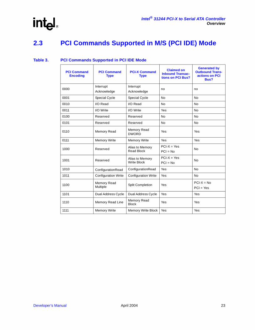
2.3 PCI Commands Supported in M/S (PCI IDE) Mode
Table 3. PCI Commands Supported in PCI IDE Mode
PCI Command Encoding
PCI Command Type
PCI-X Command Type
Claimed on Inbound Transac-tions on PCI Bus?
Generated by Outbound Trans-
actions on PCI Bus?
0000 Interrupt
Acknowledge
Interrupt
Acknowledgeno no
0001 Special Cycle Special Cycle No No
0010 I/O Read I/O Read No No
0011 I/O Write I/O Write Yes No
0100 Reserved Reserved No No
0101 Reserved Reserved No No
0110 Memory Read Memory ReadDWORD
Yes Yes
0111 Memory Write Memory Write Yes Yes
1000 Reserved Alias to Memory Read Block
PCI-X = Yes
PCI = NoNo
1001 Reserved Alias to Memory Write Block
PCI-X = Yes
PCI = NoNo
1010 ConfigurationRead ConfigurationRead Yes No
1011 Configuration Write Configuration Write Yes No
1100 Memory Read Multiple Split Completion Yes
PCI-X = No
PCI = Yes
1101 Dual Address Cycle Dual Address Cycle Yes Yes
1110 Memory Read Line Memory Read Block Yes Yes
1111 Memory Write Memory Write Block Yes Yes

24 April 2004 Developer’s Manual
Intel® 31244 PCI-X to Serial ATA ControllerOverview
2.3.1 PCI Commands Supported in DPA Mode
In DPA Mode, the SATA Unit registers are mapped in memory space using one base address register. Each port supports its own DMA and each SATA port device may be independently controlled. Table 4 shows the PCI and PCI-X commands supported for both inbound and outbound transactions when in DPA Mode.
For inbound transactions in conventional PCI, Memory Read transactions are disconnected-with-data on the first data phase. For example, when a Memory Read transaction is requesting more than one DWORD, the transaction is disconnected on the first DWORD. The GD31244 controller aliases Memory Read Line (MRL) and Memory Read Multiple (MRM) to Memory Read. Memory Write (MW) is also disconnected-with-data on the first data phase. For example, only the first DWORD is claimed and then the transaction is disconnected. The GD31244 controller aliases Memory Write and Invalidate (MWI) to Memory Write. In PCI-X mode, Memory Read Block and Memory Write Block are single-phase-disconnected.
Table 4. PCI Commands Supported in DPA Mode
PCI Command Encoding
PCI Command Type
PCI-X Command Type
Claimed on Inbound Transac-tions on PCI Bus?
Generated by Outbound Trans-actions on PCI
Bus?
0000 Interrupt
Acknowledge
Interrupt
AcknowledgeNo No
0001 Special Cycle Special Cycle No No
0010 I/O Read I/O Read No No
0011 I/O Write I/O Write No No
0100 Reserved Reserved No No
0101 Reserved Reserved No No
0110 Memory Read Memory Read DWORD Yes Yes
0111 Memory Write Memory Write Yes Yes
1000 Reserved Alias to Memory Read Block
PCI-X = Yes
PCI = NoNo
1001 Reserved Alias to Memory Write Block
PCI-X = Yes
PCI = NoNo
1010 ConfigurationRead ConfigurationRead Yes No
1011 Configuration Write Configuration Write Yes No
1100 Memory Read Multiple Split Completion Yes
PCI-X = No
PCI = Yes
1101 Dual Address Cycle Dual Address Cycle Yes Yes
1110 Memory Read Line Memory Read Block Yes Yes
1111 Memory Write Invalidate Memory Write Block Yes Yes

Developer’s Manual April 2004 25
Intel® 31244 PCI-X to Serial ATA ControllerOverview
2.4 Serial ATA Interface
Four 1.5 Gbits/s Serial ATA ports are located on the GD31244, to support point-to-point connectivity to:
• Disk Drives
• CD ROMs
• DVD ROMs
• Any other Serial ATA target device
Each port is compliant with the Serial ATA Specification. High-speed differential-duplex serial lines send 8B/10B encoded data to and from the GD31244 and the target at a maximum raw data rate of 1.2 Gbits/s (150 Mbytes/s). Copies of the target Task File Registers are maintained on the GD31244 and transferred as needed to the target. The Serial ATA protocol is software compatible with all existing operating systems that support ATA devices. However, performance and reliability are improved, since all data is CRC checked.
The GD31244 may be configured in a high-performance mode where each SATA port is addressed individually, eliminating the performance bottlenecks of Master/Slave configurations. This mode is called “Direct Port Access (DPA)” and requires enhanced software and drivers. The MS_DA input selects between Master/Slave mode (when HIGH) and DPA mode (when LOW). The SATA interface on the GD31244 supports four independent SATA ports, but may also be set up to emulate IDE Master/Slave (M/S or PCI IDE mode). IDE M/S emulation is included primarily for debugging purposes. Four 1.5 Gb/s Serial ATA ports are located on the GD31244 to support point-to-point connectivity to disk drives, CD ROMs, DVD ROMs or any other Serial ATA target device. Each port is compliant with the “Serial ATA / High Speed Serialized AT Attachment” specification, Rev. 1.0, August 29, 2001. High speed differential duplex serial lines send 8b/10b encoded data to and from the GD31244 and the target at a maximum data rate of 1.5 Gb/s (150 MB/s). Copies of the targets’ Task File Registers are maintained on the GD31244 and transferred as needed to the target. The GD31244 in M/S mode is software compatible with all existing operating systems that support ATA devices; however, performance and reliability are improved since all data is CRC checked.

26 April 2004 Developer’s Manual
Intel® 31244 PCI-X to Serial ATA ControllerOverview
As shown in Figure 2, the SATA Unit implements four SATA ports. Each SATA port connects point-to-point to a SATA device such as a hard drive device using a four-wire serial link. Each SATA port supports the following features:
• 1 KB transmit/receive FIFO
• DMA Engine with scatter/gather capability
• The SATA Unit supports two operating modes:
— PCI IDE (M/S) Mode
— Direct Port Access Mode
In M/S mode, SATA ports 1 and 2are used to emulate Master/Slave (M/S) operation for the Primary IDE Channel. Similarly, SATA ports 3 and 4 are used to emulate M/S operation for the Secondary IDE Channel. These ports are mapped in I/O Space/
In Direct Port Access Mode, each SATA port operates independently and all four SATA ports are memory-mapped contiguously using one base address register.
The GD31244 controller allows PCI masters on the PCI bus to initiate transactions to the SATA Unit ports and allows the SATA port DMAs to initiate transactions to the PCI bus. In M/S mode, the SATA Unit registers are mapped in the I/O space. Two channels (primary and secondary) are supported on the GD31244 controller. Each channel consists of four register blocks:
• Command
• Control
• DMA
• SATA Superset
PCI Base Address Register 0 points to the primary channel command block, Base Address Register 1points to the primary channel control block, Base Address Register 2 points to the secondary channel command block, Base Address Register 3 points to the secondary channel control block, Base Address Register 4 points to both of the channel DMA register, and Base Address Register 5 defines the base I/O address for the SATA superset registers. Each channel supports its own DMA controller. The DMA moves data between memory and a device on the channel. There are two devices per channel for master/slave emulation. Table 3 shows the PCI and PCI-X commands supported for both inbound and outbound transactions when in M/S Mode.
Figure 2. Serial ATA Unit Block Diagram
Disk 2
Disk 4
Disk 1
Disk 3
Port 1
Port 4
Port 3
Port 2PCI-XBus
SerialATAUnit

Developer’s Manual April 2004 27
Intel® 31244 PCI-X to Serial ATA ControllerOverview
2.5 Modes of Operation
The programming interface for the GD31244 has 2 modes of operation: Master/Slave (M/S or PCI IDE) mode and Direct Port Access (DPA) mode.
2.5.1 Master/Slave Mode (or PCI IDE Mode)
Master/Slave (M/S) mode implements a PCI-native mode standard ATA controller with primary and secondary channels, each supporting a master and a slave mass storage device (4 SATA devices in total). M/S mode places the task file in different segments of I/O space and differentiates within each space between primary and secondary channels. Base Address Register 5 (BAR5) provides access to the SATA extended register set in I/O space.
2.5.2 Direct Port Access Mode
Direct Port Access (DPA) mode is a new mass storage sub-class that extends the standard task file interface to include expandable numbers of ports and advanced DMA capabilities. Standard PCI ATA controllers share the task file interface between the master and slave device, eliminating the ability to support simultaneous access between a master/slave pair. DPA allows the GD31244 to support unique task file interfaces between multiple SATA ports. DPA eliminates the parallel ATA master/slave protocol requirements. DPA access is geared for applications where high data bandwidth and performance are primary requirements. This mode allows for simultaneous access to each SATA port for true overlapped I/O capability. Table 5 provides the primary features of the DPA mode interface.
While utilizing DPA mode to accomplish an overlapped and independent I/O capability, the block, control block, DMA and SATA superset registers for each SATA port are available at all times. DMA context is unique to each port, allowing independent and simultaneous transfers between the host and each of the SATA ports.
Table 5. DPA Mode Interface Features
Features Description
PCI up to 66 MHz or PCI-X up to 133 MHz Required for bandwidth.
Independent port operation Each SATA port can be controlled independently. Each port’s registers are available at all time. This includes DMA registers.
One DMA Channel per SATA port By having each SATA port support a DMA channel data to be transferred between device and memory independently of other devices. The DMA context can also be maintained.
Enhanced Interrupt Reporting To report Serial ATA specific events: SError bits, First Party DMA receipt.

28 April 2004 Developer’s Manual
Intel® 31244 PCI-X to Serial ATA ControllerOverview
2.5.3 Selecting DPA or M/S Mode
The GD31244 uses mode pin MS_DA to place the device in Master/Slave mode (when HIGH) or DPA mode (when LOW). This determination is made at power up so I/O and Memory can be configured correctly. Since a dynamic change in configuration memory and I/O mapping is not allowed, any mode change requires a power-on reset of the chip. As such, software control of this mode selection is not provided. The programming interface determines if the GD31244 is in M/S mode or DPA mode by reading by reading the PCI base class and the subclass values defined herein. The subclass value for the DPA mode has been assigned by the PCI SIG and is 06h.
PCI/X bus operation is programmed through the configuration register set. This includes the required PCI register set and user-defined registers that configure split transaction behavior, message signaled interrupts and other advanced features. Mass storage devices are controlled through registers accessed via the BAR interface. Registers are divided into functional sets. These are the task file, bus master and extended register sets. Depending on the mode, these sets may appear at different addresses, have different bus widths or be extended to provide additional features. See the required M/S or DPA mode section as appropriate for the application. DPA mode utilizes a single BAR in memory space to access all register sets and organizes them by channel with an additional area for common registers.
Serial ATA Direct Port Access (DPA) mode is selected when the MS_DA input is LOW. This mode provides an interface method for SATA host controllers that eliminates the parallel ATA M/S protocol requirements. DPA access is geared for applications where high data bandwidth and performance are primary requirements and software compatibility is not mandatory. This mode allows for simultaneous access to each SATA port for true overlapped I/O capability.
2.5.4 DPA Mode Port Initialization
In DPA mode, the GD31244 powers up with the serial ATA ports disabled. To enable each port, write 0 then 1 to bits 0:3 of each ports Serial Control Register. For example, to enable port 1: read BAR0 + 308h; AND the read value with FFFFFFF0h; write the result to BAR0 + 308h; “OR” the result with 000 0001h; write the result to BAR0 + 308h.
Table 6. BAR Register usage in M/S and DPA Modes
BAR DPA Mode M/S Mode
0 32-bit device base address I/O Task File Primary Command
1 32-bit device address extension (for 64-bit addresses) I/O Task File Primary Control
2 Reserved I/OTask File Secondary Command
3 Reserved I/O Task File Secondary Control
4 Reserved I/O Bus Master
5 Reserved I/O Superset Registers

Developer’s Manual April 2004 29
Intel® 31244 PCI-X to Serial ATA ControllerOverview
2.6 Serial EEPROM Interface
In add-in card applications, firmware may be downloaded to the system from a Serial EEPROM or Serial Flash ROM via the GD31244. This industry standard 4-pin interface known as SPI, allows any size of device to be connected to the GD31244 up to 128 KBytes. A typical firmware device is STMicroelectronics M25P10-A.
2.7 Extended Voltage Mode
The SATA voltages were designed primarily for a cable connection to the hard drives. In certain applications, such as NAS/SAN enclosures, the hard disk drives (HDD) are connected to a backplane, not a cable (typically in desktop systems). Due to the frequency of the SATA interface, the backplane creates a significant attenuation of the SATA signals. In an effort to simplify system designs, the GD31244 offers an extended voltage range to help alleviate this issue. This extended voltage range allows standard SATA HDD to be used with SATA backplanes. The firmware may be place into the External Voltage Mode by setting bit 14 in PHY Configuration Register Address 140H to 1. This forces the firmware to operate with this extended voltage range.
Table 7. Normal Voltage Mode
Parameter Description Minimum Maximum Units
OUT TX output differential peak-to-peak voltage swing 400 600 mVp-p
IN RX input differential peak-to-peak voltage swing 325 600 mVp-p
Table 8. Extended Voltage Mode
Parameter Description Minimum Maximum Units
OUT TX output differential peak-to-peak voltage swing 800 2000 mVp-p
IN RX input differential peak-to-peak voltage swing 175 2000
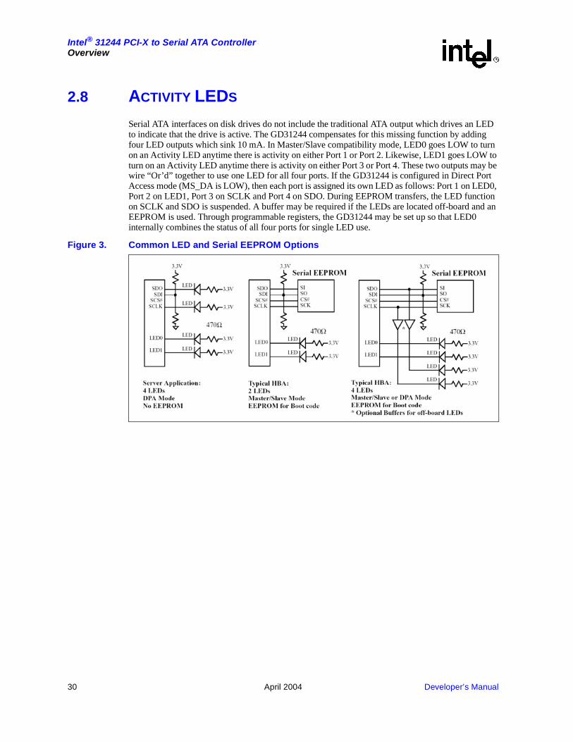
30 April 2004 Developer’s Manual
Intel® 31244 PCI-X to Serial ATA ControllerOverview
2.8 ACTIVITY LEDS
Serial ATA interfaces on disk drives do not include the traditional ATA output which drives an LED to indicate that the drive is active. The GD31244 compensates for this missing function by adding four LED outputs which sink 10 mA. In Master/Slave compatibility mode, LED0 goes LOW to turn on an Activity LED anytime there is activity on either Port 1 or Port 2. Likewise, LED1 goes LOW to turn on an Activity LED anytime there is activity on either Port 3 or Port 4. These two outputs may be wire “Or’d” together to use one LED for all four ports. If the GD31244 is configured in Direct Port Access mode (MS_DA is LOW), then each port is assigned its own LED as follows: Port 1 on LED0, Port 2 on LED1, Port 3 on SCLK and Port 4 on SDO. During EEPROM transfers, the LED function on SCLK and SDO is suspended. A buffer may be required if the LEDs are located off-board and an EEPROM is used. Through programmable registers, the GD31244 may be set up so that LED0 internally combines the status of all four ports for single LED use.
Figure 3. Common LED and Serial EEPROM Options

Developer’s Manual April 2004 31
Intel® 31244 PCI-X to Serial ATA ControllerOverview
2.8.1 Reference Clock Generation
A 37.5 MHz reference clock with a +/- 100 ppm accuracy is required for proper operation of the GD31244. This can be generated from an external oscillator connected directly to the XI input. Optionally, a 37.5 MHz crystal may be connected between the XI and XO pins with a 20 pF capacitor from XI to ground and another from XO to ground. The crystal should have the following characteristics:
• Frequency: 37.5 MHz +/- 100 ppm
• Mode: Fundamental
• Type: “Parallel” resonant
• ESR: 30 Ohms maximum
• Load Capacitance: 20 pF
• Shunt Capacitance: 7 pF
• Drive Level:500 mW maximum
Recommended Vendor/Part Number: Fox Electronics, Part number: 278-37.5-8 (This is an HC-49SD surface mountable package.) The crystal should be placed near the GD31244 and isolated from noisy circuits as much as possible.
2.9 High-End Storage Features
The GD31244 is well suited for high-end storage applications using Serial ATA drives. The Serial ATA Direct Port Access mode described above allows the host CPU to initiate overlapping operations to all four drives. Another feature is a “wide-swing mode” on the four transmitter outputs which provides approximately double the amplitude of normal operation. This increase differential voltage swing is useful in connecting to Serial ATA devices over backplanes or between systems.
2.10 JTAG Interface
An IEEE 1149.1 compatible JTAG interface and boundary scan functionality is provided to assist onboard testing of the device.GD31244

32 April 2004 Developer’s Manual
Intel® 31244 PCI-X to Serial ATA ControllerSerial EEPROM
Serial EEPROM 3
The GD31244 is software compatible with all existing operating systems which support parallel ATA devices. However, the additional functions offered by the GD31244 require OS-specific code to take advantage of these beneficial functions. The code for initializing the system and booting drives will normally be located within the BIOS of the Host system or with an expansion ROM on the Host Bus Adapter card. A Serial EEPROM may be optionally connected to the GD31244 to store this code which will be downloaded and executed by the host system during initialization. Applications not requiring a downloadable program do not require the Serial EEPROM. The program should be downloaded into system RAM and executed there. Execution from the EEPROM should not be attempted. Details on expansion ROM operation and initialization may be found in the PCI 2.2 specification, Section 6.3.
The Intel GD31244 contains a four pin, Serial Peripheral Interface (SPI) to connect to an optional Serial EEPROM to store a downloadable program. At power-up, the GD31244 hardware automatically detects whether the EEPROM is present and indicates to this status to the Host System during initialization.
This SPI interface was designed for compatibility with an ST Microelectronics* M25P10-A or Atmel* AT25F1024 device with 131,072 Bytes of memory or an equivalent device. For the purposes of understanding Serial EEPROM operation, refer to the Datasheet for the ST Microelectronics documents, M25P10-A (dated February 2002) and Application Note (AN-1511 Ensuring Compatibility Between M25P10 to M25P10-A and M25P05 to M25P05-A in Your Application, dated February 2002) and the datasheet for the Atmel AT25F1024 (revision 1440G, dated February, 2002). The basic connection is shown in Figure 4.
Figure 4. Serial EEPROM Interface
B1396-001
Serial EEPROM
SDOSDI
SCS#SCLK
SISOCS#SCK
WP#
HOLD#
User Selectable
High
GD31244

Developer’s Manual April 2004 33
Intel® 31244 PCI-X to Serial ATA ControllerSerial EEPROM
Note: The SDI, SDO and SCLK pins have multiple functions an may require additional functionality as presented in Table 9. WP# is not documented here. Refer to the vendors’ datasheet.
The GD31244 is a Master SPI device which outputs three signals (SCS#, SCLK and SDO) and inputs one signal (SDI). Only one external device is supported. The SCLK is derived from the PCI/PCI-X bus CLK signal as presented in Table 10. The GD31244 behaves as if the SPI modes are CPOL=0 and CPHA=0.
The Serial EEPROM implements the nine commands presented in Table 11. These commands are supported through the GD31244, either through the PCI Configuration space (offsets 90h and 94h) or the memory interface.
Table 9. Serial EEPROM Interface Pins
Name Description
SDI
INPUT - LVTTL with Pull Up: Connects to the serial data output (SO) of the Serial EEPROM. Data is shifted out of the EEPROM on the falling edge of SCLK. Customers are recommended to add pads for both a pull-up and a pull-down resistor for possible use in the future.
SDOOUTPUT - LVTTL: Connects to the serial data input (SI) of the Serial EEPROM. Data is latched into the Serial EEPROM on the rising edge of SCLK. This is also the activity output for Channel 3 when all four LEDs are activated (active LOW).
SCLK OUTPUT - LVTTL: Connects to the clock input (SCK) of the Serial EEPROM. This is also the activity LED output for Channel 2 when all four LEDs are activated (active LOW).
SCS# OUTPUT - LVTTL with Pull Up: Connects to the chip select input (CS#) of the Serial EEPROM.
Table 10. SCLK Frequency
PCI-X Speed SCLK Period Divider
PCI 33 MHz 8.25 MHz 121 nsec 4
PCI-X 66 MHz 16.5 MHz 60.6 nsec 4
PCI-X 100 MHz 12.5 MHz 80 nsec 8
PCI-X 133 MHz 16.625 MHz 60.2 nsec 8
Table 11. Serial EEPROM Commands
Command Name Op_Code Access Operation
WRSR 01h - 0000 0001 PCI Config Write Status Register
PROGRAM 02h - 0000 0010 Memory Program Data into Memory Array
READ 03h - 0000 0011 Memory Read Data from Memory Array
WRDI 04h - 0000 0100 PCI Config Reset Write Enable Latch
RDSR 05h - 0000 0101 PCI Config Read Status Register
WREN 06h - 0000 0110 PCI Config Set Write Enable Latch
RDID 15h - 0001 0101 PCI Config Read Manufacturer and Product ID
SECTOR ERASE 52h - 0101 0010 PCI Config Erase One Sector in Memory Array
CHIP ERASE 62h - 0110 0010 PCI Config Erase the entire Memory Array

34 April 2004 Developer’s Manual
Intel® 31244 PCI-X to Serial ATA ControllerSerial EEPROM
3.1 Write Status Register (WRSR) Command
The WRSR command allows the user to control three bits within the EEPROM status register relating to write protection: WPEN, BP1 and BP0. The EEPROM is divided into four sectors that may be selectively write protected sectors where the top quarter (1/4), top half (1/2), or all of the memory sectors may be protected (locked out) from write. The AT25F512 is divided into two sectors where all of the memory sectors may be protected (locked out) from write. Any of the locked-out sec-tors will therefore be READ only. The locked-out sector and the corresponding status register control bits are presented in Table 12.
The three bits, BP0, BP1, and WPEN, are nonvolatile cells that have the same proper-ties and functions as the regular memory cells (e.g., WREN, t WC, RDSR).
The WRSR command also allows the user to enable or disable the Write Protect (WP) pin through the use of the Write Protect Enable (WPEN) bit. Hardware write protection is enabled when the WP pin is low and the WPEN bit is 1. Hardware write protection is disabled when either the WP pin is high or the WPEN bit is 0. When the device is hard-ware write protected, writes to the Status Register, including the Block Protect bits and the WPEN bit, and the locked-out sectors in the memory array are disabled. Write is only allowed to sectors of the memory which are not locked out. The WRSR command is self-timed to automatically erase and program BP0, BP1, and WPEN bits. In order to write the status register, the device must first be write enabled through the WREN command. Then, the command and data for the three bits are entered. During the internal write cycle, all commands will be ignored except RDSR commands. The AT25F512/1024 will automatically return to write disable state at the completion of the WRSR cycle. The WRSR operation is shown in Figure 5.
Note: When the WPEN bit is hardware write protected, it cannot be changed back to 0, as long as the WP pin is held low.
Table 12. Block Write Protect Bits
Level
Status Bit Registers AT25F512 AT25F1024
BP1 BP0 Array Addresses Locked Out Locked-out Sectors Array Addresses
Locked Out Locked-out Sectors
0 0 0
None None
None None
1 (1/4) 0 1 018000 - 01FFFF Sector 4
2 (1/2) 1 0 010000 - 01FFFF Sector 3, 4
3 (All) 1 1 000000 - 00FFFF All sectors (1-2) 000000 - 01FFFF All sectors (1-4)
Figure 5. Write Status Register (WRSR) Operation
SCS#
SCLK
SDO
SDI
0 1 2 3 4 5 6 7 8 9 10 11 12 13 14 15
Hi -Z
10 0 0 0 0 00 7 6 5 4 3 2 1 0
WPENReserved- Write as 0Reserved- Write as 0Reserved-Write as 0
RDY# - Write as 0WEN - Write as 0BP0 - Block Write Protect bit 0BP1 - Block Write Protect bit 1
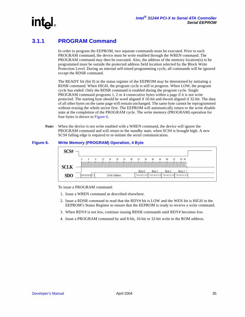
Developer’s Manual April 2004 35
Intel® 31244 PCI-X to Serial ATA ControllerSerial EEPROM
3.1.1 PROGRAM Command
In order to program the EEPROM, two separate commands must be executed. Prior to each PROGRAM command, the device must be write enabled through the WREN command. The PROGRAM command may then be executed. Also, the address of the memory location(s) to be programmed must be outside the protected address field location selected by the Block Write Protection Level. During an internal self-timed programming cycle, all commands will be ignored except the RDSR command.
The READY bit (bit 0) in the status register of the EEPROM may be determined by initiating a RDSR command. When HIGH, the program cycle is still in progress. When LOW, the program cycle has ended. Only the RDSR command is enabled during the program cycle. Single PROGRAM command programs 1, 2 or 4 consecutive bytes within a page if it is not write protected. The starting byte should be word aligned if 16-bit and dword aligned if 32-bit. The data of all other bytes on the same page will remain unchanged. The same byte cannot be reprogrammed without erasing the whole sector first. The EEPROM will automatically return to the write disable state at the completion of the PROGRAM cycle. The write memory (PROGRAM) operation for four bytes is shown in Figure 6.
Note: When the device is not write enabled with a WREN command, the device will ignore the PROGRAM command and will return to the standby state, when SCS# is brought high. A new SCS# falling edge is required to re-initiate the serial communication.
To issue a PROGRAM command:
1. Issue a WREN command as described elsewhere.
2. Issue a RDSR command to read that the RDY# bit is LOW and the WEN bit is HIGH in the EEPROM’s Status Register to ensure that the EEPROM is ready to receive a write command.
3. When RDY# is not low, continue issuing RDSR commands until RDY# becomes low.
4. Issue a PROGRAM command by and 8-bit, 16-bit or 32-bit write to the ROM address.
Figure 6. Write Memory (PROGRAM) Operation, 4 Byte
SCS#
SCLK
SDO
0 4 8 2012 16 24
0
28 32 36 40 44 48 52
0 0 0 0 0 11 23-bit Address 7 6 5 4 3 2 1 0
Byte 07 6 5 4 3 2 1 0
Byte 17 6 5 4 3 2 1 0
Byte 27 6 5 4 3 2 1 0
Byte 3
54 56

36 April 2004 Developer’s Manual
Intel® 31244 PCI-X to Serial ATA ControllerSerial EEPROM
3.1.2 READ Command
The EEPROM contains the downloadable programs needed in plug-in expansion card applications. Normally, after the card is configured, the Host system downloads the program from the EEPROM to RAM and executes from there.
Upon a ROM memory read, the GD31244 initiates an EEPROM READ operation at the memory location addressed by the PCI bus. The PCI/PCI-X memory address is translated into the 17-bit EEPROM memory address by the GD31244. Bits 23-17 of the EEPROM address are set to 0. Bits 16-0 of the EEPROM address are identical to the address on the PCI/PCI-X bus. The byte enables determine how many bytes will be read from the EEPROM (1, 2 or 4). The byte enables on ROM memory reads is presented in Table 13. The read memory (READ) operation for four bytes is shown in Figure 7.
The READ command may only be issued when the EEPROM is ready to accept a new command. When the device is busy, it cannot accept any new commands except RDSR.
To issue a READ command:
1. Issue a RDSR command to read that the RDY# bit is LOW in the EEPROM’s Status Register to ensure that the EEPROM is ready to receive a new command.
2. When RDY# is not LOW, continue issuing RDSR commands until RDY# becomes LOW.
3. Issue the READ command by performing a byte, word or double word read of the ROM at the desired address.
In PCs which are downloading the program stored in the EEPROM, the RDSR commands mentioned above will NOT be issued prior to a Read. This is acceptable during normal operation since the EEPROM will not be busy at this time.
When a READ command is issued while the EEPROM is busy, the EEPROM will return data which is all zero.
Table 13. Byte Enables on ROM Memory Reads
C/BE#3 C/BE#2 C/BE#1 C/BE#0 Length (Bytes) EEPROM A1 bit EEPROM A0 bit
1 1 1 0 1 0 0
1 1 0 1 1 0 1
1 0 1 1 1 1 0
0 1 1 1 1 1 1
1 1 0 0 2 0 0
0 0 1 1 2 1 0
0 0 0 0 4 0 0
NOTE: The access must be word aligned if 16-bit and dword aligned if 32-bit.
Figure 7. Read Memory (READ) Operation, 4 Byte
SCS#
SCLK
SDO
SDI
0 4 8 2012 16 24
Hi -Z
0
28 32 36 40 44 48 52
Hi -Z
0 0 0 0 0 11 23-bit Address
7 6 5 4 3 2 1 0
Byte 07 6 5 4 3 2 1 0
Byte 17 6 5 4 3 2 1 0
Byte 27 6 5 4 3 2 1 0
Byte 3
54 56

Developer’s Manual April 2004 37
Intel® 31244 PCI-X to Serial ATA ControllerSerial EEPROM
3.1.3 Write Disable (WRDI) Command
To protect the device against inadvertent writes, the WRDI command disables further write commands. The WRDI command is independent of the status of the WP pin. The write disable (WRDI) operation is shown in Figure 8.
The WRDI command may only be issued when the EEPROM is ready to accept a new command. When the device is busy, it cannot accept any new commands except RDSR.
To issue a WRDI command:
1. Issue a RDSR command to read that the RDY# bit is LOW in the EEPROM’s Status Register to ensure that the EEPROM is ready to receive a new command.
2. When RDY# is not LOW, continue issuing RDSR commands until RDY# becomes LOW.
3. Issue the WRDI command with an 8-bit write of 04h to the SPI Command Register at offset 90h.
Figure 8. Write Disable (WRDI) Operation
SCS#
SCLK
SDO
SDI
0 0 0 0 0 1 0 0
Hi -Z
0 1 2 3 4 5 6 7

38 April 2004 Developer’s Manual
Intel® 31244 PCI-X to Serial ATA ControllerSerial EEPROM
3.1.4 Read Status Register (RDSR) Command
The RDSR command reads the EEPROM’s status register. This is the most commonly issued command since the status register must be polled in order to determine that a previously issued command is complete and the device is ready to accept a new command. The real-time ready (RDY#) and write enable (WEN) status bits of the EEPROM may be determined by the RDSR command. Likewise, the write protect (WPEN) and block protect bits (BP1 and BP0) may also be read. These three bits are non-volatile memory cells which are set using the WRSR command. During internal write cycles, all other commands will be ignored except the RDSR command. The read status (RDSR) operation is shown in Figure 9. The status register format is presented in Table 14.
The RDSR command is unique in that it is always serviced by the EEPROM even if a previous command has yet to complete.
To issue a RDSR command:
1. Issue an 8-bit write of 05h to the SPI Command Register at offset 90h.
2. Read an 8-bit value from the SPI Data register at offset 94h.
Figure 9. Read Status Register (RDSR) Operation
SCS#
SCLK
SDO
SDI
0 1 2 3 4 5 6 7 8 9 10 11 12 13 14
0 0 0 0 0 1 0 1
7 6 5 4 3 2 1 0Hi -Z Hi -Z
WPEN: Write Protect control bitReservedReservedReserved
RDY# - Ready bitWEN - Write Enable statusBP0 - Block Write Protect bit 0BP1 - Block Write Protect bit 1
Table 14. Status Register Format (Refer to Atmel* AT25F1024 Datasheet)
Bit Name Description
7 WPEN When HIGH, allows override of the hardware write protect pin.
6-4 Reserved These bits are LOW when the device is not in a write cycle. Write with ‘0’.
3
2
BP1
BP0
These two bits control which sectors of the chip are write protected:
00 - None
01 - Sector 4
10 - Sectors 3 & 4
11 - All sectors
1 WEN When LOW, the device is write protected. When HIGH, the device is write enabled.
0 RDY# When LOW, the device is READY. When HIGH, a write cycle is in progress.
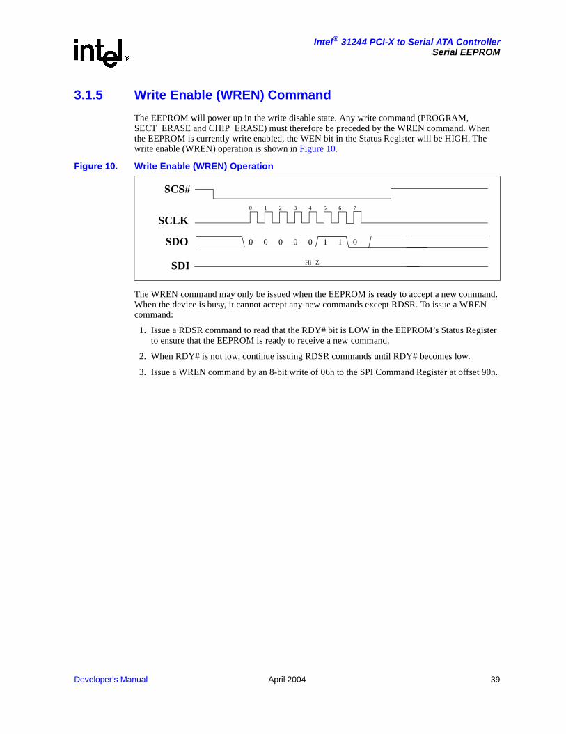
Developer’s Manual April 2004 39
Intel® 31244 PCI-X to Serial ATA ControllerSerial EEPROM
3.1.5 Write Enable (WREN) Command
The EEPROM will power up in the write disable state. Any write command (PROGRAM, SECT_ERASE and CHIP_ERASE) must therefore be preceded by the WREN command. When the EEPROM is currently write enabled, the WEN bit in the Status Register will be HIGH. The write enable (WREN) operation is shown in Figure 10.
The WREN command may only be issued when the EEPROM is ready to accept a new command. When the device is busy, it cannot accept any new commands except RDSR. To issue a WREN command:
1. Issue a RDSR command to read that the RDY# bit is LOW in the EEPROM’s Status Register to ensure that the EEPROM is ready to receive a new command.
2. When RDY# is not low, continue issuing RDSR commands until RDY# becomes low.
3. Issue a WREN command by an 8-bit write of 06h to the SPI Command Register at offset 90h.
Figure 10. Write Enable (WREN) Operation
SCS#
SCLK
SDO
SDI
0 0 0 0 0 1 1 0
Hi -Z
0 1 2 3 4 5 6 7

40 April 2004 Developer’s Manual
Intel® 31244 PCI-X to Serial ATA ControllerSerial EEPROM
3.1.6 Sector Erase (SECT_ERASE) Command
Before an EEPROM byte may be reprogrammed, the sector that contains the byte must be erased. In order to erase the EEPROM, two separate commands must be executed. First, the device must be write enabled through the WREN command, then the SECT_ERASE command may be executed. The SECT_ERASE command is internally controlled; it will automatically be timed to completion. During this time, all commands will be ignored, except RDSR command. The EEPROM will automatically return to the write disable state at the completion of the SECT_ERASE cycle.
The SECT_ERASE command erases every byte in the selected sector if the sector is not Write-Protected. The EEPROM Sector address (bits 16 & 15) is determined by two bits in the SPI Command Register at offset 91h: spi_sect_addr1 (mapped to bit 16) and spi_sect_addr0 (mapped to bit 15). These bits form the uppermost bits of the memory address and split the memory into the four sectors. Address bits 23-17 are LOW. The sector erase (SECT_ERASE) operation is shown in Figure 11.
To issue a SECT_ERASE command:
1. Issue a WREN command as described in Section 3.1.5.
2. Issue a RDSR command to read that the RDY# bit is LOW and the WEN bit is HIGH in the EEPROM’s Status Register to ensure that the EEPROM is ready to receive a write command.
3. When RDY# is not low, continue issuing RDSR commands until RDY# becomes low.
4. Issue a SECT_ERASE command by an 8-bit write of 52h to the SPI Command Register at offset 90h.
Figure 11. Sector Erase (SECT_ERASE) Operation
SCS#
SCLK
SDO
SDI
0 4 8 2012 16 24
Hi -Z
0
28 32 36 40 44 48 52
Hi -Z
0 0 0 0 0 11 23-bit Address
7 6 5 4 3 2 1 0
Byte 07 6 5 4 3 2 1 0
Byte 17 6 5 4 3 2 1 0
Byte 27 6 5 4 3 2 1 0
Byte 3
54 56
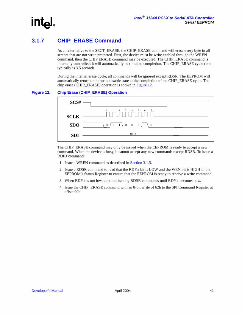
Developer’s Manual April 2004 41
Intel® 31244 PCI-X to Serial ATA ControllerSerial EEPROM
3.1.7 CHIP_ERASE Command
As an alternative to the SECT_ERASE, the CHIP_ERASE command will erase every byte in all sectors that are not write protected. First, the device must be write enabled through the WREN command, then the CHIP ERASE command may be executed. The CHIP_ERASE command is internally controlled; it will automatically be timed to completion. The CHIP_ERASE cycle time typically is 3.5 seconds.
During the internal erase cycle, all commands will be ignored except RDSR. The EEPROM will automatically return to the write disable state at the completion of the CHIP_ERASE cycle. The chip erase (CHIP_ERASE) operation is shown in Figure 12.
The CHIP_ERASE command may only be issued when the EEPROM is ready to accept a new command. When the device is busy, it cannot accept any new commands except RDSR. To issue a RDID command:
1. Issue a WREN command as described in Section 3.1.5.
2. Issue a RDSR command to read that the RDY# bit is LOW and the WEN bit is HIGH in the EEPROM’s Status Register to ensure that the EEPROM is ready to receive a write command.
3. When RDY# is not low, continue issuing RDSR commands until RDY# becomes low.
4. Issue the CHIP_ERASE command with an 8-bit write of 62h to the SPI Command Register at offset 90h.
Figure 12. Chip Erase (CHIP_ERASE) Operation
SCS#
SCLK
SDO
SDI
0 1 1 0 0 0 1 0
Hi -Z
0 1 2 3 4 5 6 7

42 April 2004 Developer’s Manual
Intel® 31244 PCI-X to Serial ATA ControllerSerial EEPROM
3.1.8 Read ID Register (RDID) Command
The RDID command allows the user to read the manufacturer and product ID of the EEPROM. The first byte after the command will be the manufacturer code (e.g., 1Fh = Atmel*), followed by the device code. The read ID register (RDID) operation is shown in Figure 13.
The RDID command may only be issued when the EEPROM is ready to accept a new command. When the device is busy, it cannot accept any new commands except RDSR. To issue a RDID command:
1. Issue a RDSR command to read that the RDY# bit is LOW in the EEPROM’s Status Register to ensure that the EEPROM is ready to receive a new command.
2. When RDY# is not LOW, continue issuing RDSR commands until RDY# becomes LOW.
3. Issue the RDID command with an 8-bit write of 15h to the SPI Command Register at offset 90h.
4. Upon completion of the RDID command, the 8-bit Manufacturer’s ID (1Fh for Atmel) will be located in bits 7:0 of the SPI Data Register (offset 94h) and the 8-bit Device ID (060h for AT25F1024) will be located in bits 15:8 of the SPI Data Register (offset 94h).
Figure 13. Read ID Register (RDID) Operation
SCS#
SCLK
SDO
SDI
0 1 2 3 4 5 6 7 8 9 10 11 12 13 14 15
Hi -Z
0 0 0 0 0 0 0 1
Manufacturer ID
16 17 18 19 20 21 22
Device ID
Hi -Z7 6 5 4 3 2 1 0 7 6 5 4 3 2 1 0

Developer’s Manual April 2004 43
Intel® 31244 PCI-X to Serial ATA ControllerSerial EEPROM
3.1.9 Serial EEPROM SPI Interface – Address 90h
3.1.9.1 Programming Details
This module implements a controller for interfacing to a serial EEPROM using the SPI (Serial Peripheral Interface) standard. The controller sits between a PCI core's application interface and the serial device. It contains a state machine that accesses the ROM 1, 2 or 4 times for each PCI transaction based on the byte enables.
Reads and writes are done through the PCI expansion port defined by CR30 in configuration space.
Reads from the serial device are very slow. The controller outputs a FIFO write signal to the PCI core upon completion of the read operation. Since the FIFO is empty until this time, the host read transaction will time-out and be retried by the PCI chipset until the controller writes the data into the FIFO. The design will fail if the host aborts retries or reorders transactions to the PCI target. A burst read transaction will be slowed down into a repetition of {retry, retry, ..., retry, read 1 data phase then disconnect without data}.
Writes to the serial device must be performed by a special device driver that polls the device status register to determine when the write is done. The next write may then be executed. Each write is composed of two operations. The host must issue a write enable command followed by a write data command of 1, 2 or 4 bytes. Burst writes are not allowed. Furthermore, the set of all write pairs must be proceeded by one of the two erase commands. When the host attempts to write a subsequent data value before the first completes, the PCI core will complete the transaction and queue up the FIFO. The queue comes into play when the PCI bus write transaction period is less than the static target state machine cycle time and FIFO starts to fill up. To avoid overflowing the queue and causing the host to do retries, the serial EPROM write driver should not issue a subsequent write until the current one is complete.
The host issues all commands except the read command through a register set in configuration space. The register set is composed of command, control and data registers. The host writes the command type to the command register after setting up the control and data registers as necessary. The controller starts when the command register is written. The host then polls the status register to determine when the command is complete. For read commands, except READ, the data register will contain the result when done.

44 April 2004 Developer’s Manual
Intel® 31244 PCI-X to Serial ATA ControllerSerial EEPROM
The RDID value is for the Atmel* 25F1024 device. Other devices will have different values.
The legal values for the PCI byte enables on read and write operations are presented in Table 16.
Table 15. Write and Read Command Types
Command Type inst [7:0] ctrl [1:0] data [15:0] Description
Write
WREN 06h - - Write Enable
WRDI 04h - - Write Disable
WRSR 01h - {XX, status [7:0]} Write Status
PROGRAM † 02h - - Write Data
SECT_ERASE 52h a [16:15] - Erase 1/4 Chip
CHIP_ERASE 62h - - Erase All Chip
Read
RDSR 05h - {00h, status [7:0]} Read Status
READ † 03h - - Read Data
RDID 15h - 601Fh Read ID
† The PROGRAM and READ commands are done through the expansion ROM port of the PCI device. All other commands are done through the configuration register set.
Table 16. PCI Byte Enables on Read and Write Operations
byte_enables_n
3 2 1 0 count a [1:0]
1 1 1 0 1 0
1 1 0 1 1 1
1 0 1 1 1 2
0 1 1 1 1 3
1 1 0 0 2 0
0 0 1 1 2 2
0 0 0 0 4 0

Developer’s Manual April 2004 45
Intel® 31244 PCI-X to Serial ATA ControllerSerial EEPROM
3.1.9.2 SPI Command / Control / Status Register - Address 90h
3.1.9.2.1 SPI Command
3.1.9.2.2 SPI Control
3.1.9.2.3 SPI Status
Table 17. SPI Command
Master / Slave Mode and Direct Port Access Mode
Bits Type Reset Description
7:0 r/w 00h
Expansion ROM SPI interface command type. A write to this register
initiates the command. The status register bit D0 must be polled to
determine when the command is complete.
06h = WREN (Write Enable)
04h = WRDI (Write Disable)
01h = WRSR (Write Status)
02h = No action (SPI PROGRAM command)
52h = SECT_ERASE (Sector Erase)
62h = CHIP_ERASE (All Sector Erase)
05h = RDSR (Read Status)
03h = No action (SPI READ command)
15h = RDID (Read ID)
Others = No action
Table 18. SPI Control
Master / Slave Mode and Direct Port Access Mode
Bits Type Reset Description
15:10 r/- 00h Reserved.
9:8 r/w 00b Sector address [1:0]. Selects one of four sectors for the sector erase command 52h.
Table 19. SPI Status
Master / Slave Mode and Direct Port Access Mode
Bits Type Reset Description
23:17 r/- 00h Reserved.
16 r/- 0bCommand done. When HIGH, this indicates that the last command has been communicated to the serial device. It does not indicate the device is ready. The RDSR command must be issued to determine this.

46 April 2004 Developer’s Manual
Intel® 31244 PCI-X to Serial ATA ControllerSerial EEPROM
3.1.9.3 SPI Data Register - Address 94h
This is a multifunction register used by three commands. For the RDID command, it is a read-only register with the Manufacturer’s ID and Device ID in the upper and lower bytes respectively. For the WRSR/RDSR commands, the lower byte is a write/read register with the bit definitions presented in Table 20. The WPEN command is not applicable if the serial EEPROM device has its write protect pin WPB inactive high. Refer to the serial EEPROM device specification for how to use these bits.
3.1.10 Detection of the EEPROM at Power-Up
Immediately after power-on reset (an internal event based upon the power supply exceeding a minimum voltage), the GD31244 reads the EEPROM through the SPI interface to determine if an EEPROM is present.
Table 20. SPI Data Register - Address 94h
Master / Slave Mode and Direct Port Access Mode
Bits Type Reset Description
31:16 r/- 0 Reserved.
15:8 r/- 00h Device ID for the RDID command.
7:0 r/- 00h Manufacturer’s ID for the RDID command.
7
6
5
4
3
2
1
0
r/w 00h
WPEN External WPB pin override
Reserved
Reserved
Reserved
BP1 Block Protect 1
BP0 Block Protect 0
WEN Write Enable
RDYn Ready Active LOW

Developer’s Manual April 2004 47
Intel® 31244 PCI-X to Serial ATA ControllerSerial EEPROM
This Page Left Intentionally Blank

48 April 2004 Developer’s Manual
Intel® 31244 PCI-X to Serial ATA ControllerFunctional Blocks
Functional Blocks 4
4.1 Serial ATA
This section describes the Serial ATA (SATA) unit, including the operation modes and setup. Throughout this section, this unit is referred to as the SATA Unit or SU. The SATA Unit on 31244 supports four independent SATA ports, but may also be set up to emulate IDE master/slave.
With Parallel ATA (PATA), the controller and the device communicate using a 40-pin ribbon cable. The controller and device are connected through a parallel bus, which provides address, controls, and data signals. There are two register blocks on an ATA device:
Command Block Registers:The command block registers are used for normal data transfer requests.
Control Block Registers: The control block registers are used for device control such as software reset, and bist.
For example, the command block registers are used to issue commands to the device. The parallel interface also provides a DMA interface. Data may be exchanged between the controller and the device using either DMA or Programmed I/O (PIO). Refer to the AT Attachment with Packet Interface-6 (ATA/ATAPI-6) Specification.
SATA maintains the same programming interface. For example, the application still accesses the device with the same set of registers (Command Block Registers and Control Block Registers). Since the link between the controller and device is now serial, the device registers are now manipulated indirectly, requiring that the controller maintains a copy of all the device registers called the Shadow Register Block (SRB).
The serial bus defines a simple protocol for exchanging messages between the controller and the device. The serial protocol is transparent to the programmer. For example, the programmer does not have to be cognizant of how the serial protocol transmit and receive data. Refer to the Serial ATA Specification.
Information is exchanged between the controller and device over the serial bus using Frame Information Structures (FISs). The Serial ATA protocol defines a set of FIS:
• Register: Bidirectional
• DMA Activate: Device-to-Host
• DMA Setup: Bidirectional
• BIST Activate: Bidirectional
• Set Device Bits: Device-to-Host
• PIO Setup: Device-to-Host
• Data: Bidirectional
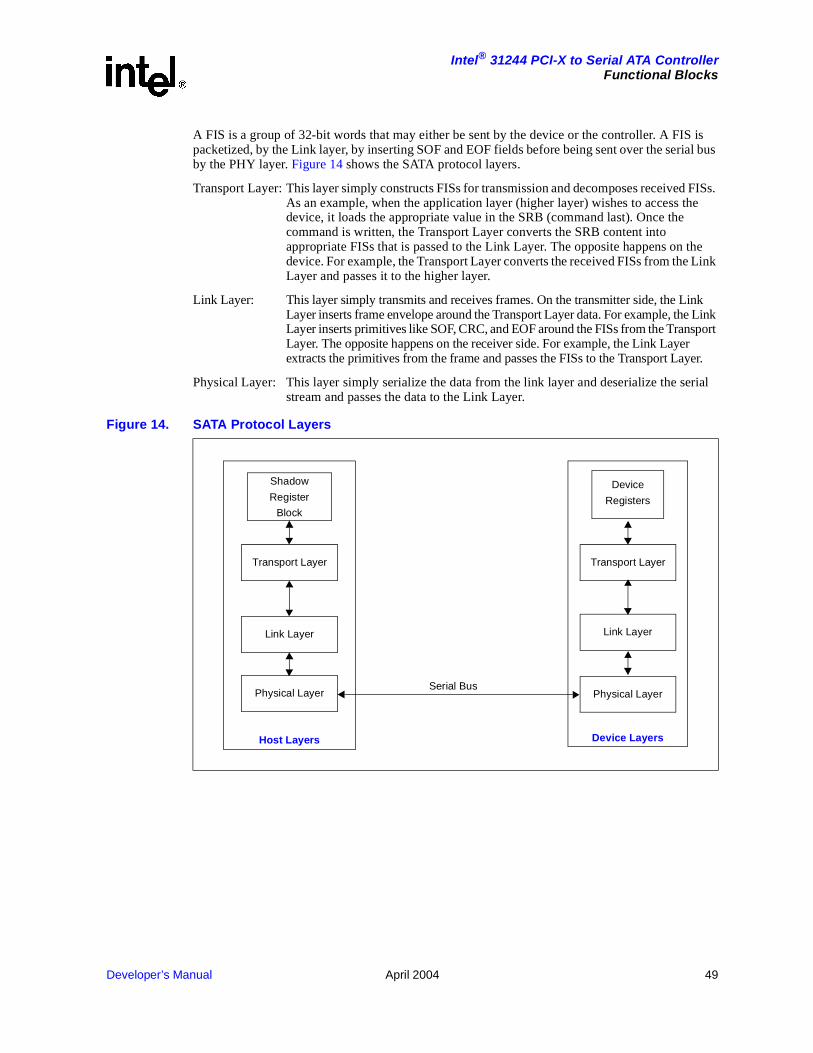
Developer’s Manual April 2004 49
Intel® 31244 PCI-X to Serial ATA ControllerFunctional Blocks
A FIS is a group of 32-bit words that may either be sent by the device or the controller. A FIS is packetized, by the Link layer, by inserting SOF and EOF fields before being sent over the serial bus by the PHY layer. Figure 14 shows the SATA protocol layers.
Transport Layer: This layer simply constructs FISs for transmission and decomposes received FISs. As an example, when the application layer (higher layer) wishes to access the device, it loads the appropriate value in the SRB (command last). Once the command is written, the Transport Layer converts the SRB content into appropriate FISs that is passed to the Link Layer. The opposite happens on the device. For example, the Transport Layer converts the received FISs from the Link Layer and passes it to the higher layer.
Link Layer: This layer simply transmits and receives frames. On the transmitter side, the Link Layer inserts frame envelope around the Transport Layer data. For example, the Link Layer inserts primitives like SOF, CRC, and EOF around the FISs from the Transport Layer. The opposite happens on the receiver side. For example, the Link Layer extracts the primitives from the frame and passes the FISs to the Transport Layer.
Physical Layer: This layer simply serialize the data from the link layer and deserialize the serial stream and passes the data to the Link Layer.
Figure 14. SATA Protocol Layers
Transport Layer
Link Layer
Physical Layer
Transport Layer
Link Layer
Physical Layer
Device
Registers
Shadow
Register
Block
Host Layers Device Layers
Serial Bus

50 April 2004 Developer’s Manual
Intel® 31244 PCI-X to Serial ATA ControllerFunctional Blocks
4.1.1 Out-of-Band Signaling
There are three Out-Of-Band (OOB) signals defined as part of the Analog Front End (AFE) layer of the PHY block:
• COMRESET
• COMINIT
• COMWAKE
These OOB signals are internal output from the receive AFE portion of the PHY and they are generated based on the detection of burst patterns of ALIGN primitives. Figure 15 shows a block diagram of the AFE cabling and the origin of the OOB signals.
COMRESET and COMINIT have the same burst characteristics except that COMRESET originates from the host controller whereas COMINIT originates from the device. COMWAKE is different from COMRESET and COMINIT by having a different idle duration between bursts. Figure 16 shows the burst patterns timings.
Figure 15. Analog Front End (AFE) Cabling and OOB Signals
Figure 16. OOB Signals Timings
B1398-01
COMRESET / COMINIT
COMWAKE 106.7 ns
320 ns106.7 ns
106.7 ns

Developer’s Manual April 2004 51
Intel® 31244 PCI-X to Serial ATA ControllerFunctional Blocks
COMRESET is used by the controller to achieve two things:
• Initialize the serial bus to establish the communication link
• Hardware reset the device
Because of the nature of the serial bus, the serial bus has to be initialized before communication between the controller and the device may occur. The controller initiates a COMRESET on the serial bus to begin the initialization sequence. After the initialization sequence is completed, the communication link between the controller and the device is established and normal operation may begin. COMRESET is also used to cause a hardware reset of the device. Figure 17 shows a COMRESET sequence.
Figure 17. COMRESET Sequence
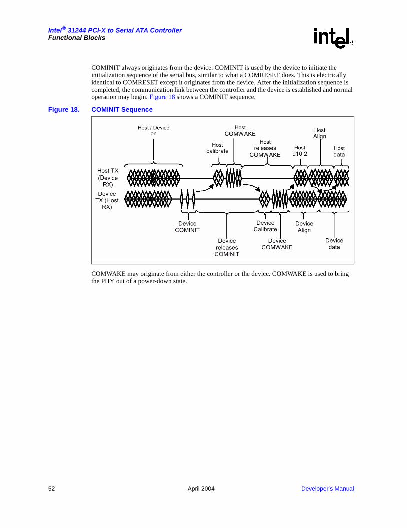
52 April 2004 Developer’s Manual
Intel® 31244 PCI-X to Serial ATA ControllerFunctional Blocks
COMINIT always originates from the device. COMINIT is used by the device to initiate the initialization sequence of the serial bus, similar to what a COMRESET does. This is electrically identical to COMRESET except it originates from the device. After the initialization sequence is completed, the communication link between the controller and the device is established and normal operation may begin. Figure 18 shows a COMINIT sequence.
COMWAKE may originate from either the controller or the device. COMWAKE is used to bring the PHY out of a power-down state.
Figure 18. COMINIT Sequence

Developer’s Manual April 2004 53
Intel® 31244 PCI-X to Serial ATA ControllerFunctional Blocks
4.2 Operational Blocks
Each SATA port on the GD31244 controller contains the following blocks:
• Serial Engine
• Register Interface
• DMA Controller
• Programmed I/O (PIO) Interface
Figure 19. SATA Port Block Diagram
FIFO
Bus
Interface
TransportLayer
LinkLayer
PHYLayer
device
Block
Control
SupersetRegisters
Command
DMA
PIO
Block
Registers
Registers

54 April 2004 Developer’s Manual
Intel® 31244 PCI-X to Serial ATA ControllerFunctional Blocks
4.2.1 Serial Engine
The Serial Engine is transparent to the user. The Serial Engine consists of the three layers:
• Transport Layer
• Link Layer
• PHY Layer
Refer to the Serial ATA Specification for more details.
4.2.2 Register Interface
The GD31244 may be set up to operate in one of the following modes:
• PCI IDE Mode (legacy M/S)
• PCI Direct Port Access Mode
The register interface for each mode is described in Section , “The SATA Unit may be set up during system reset to execute in one of the following modes. Each mode provides a different programming interface. The DPA_MODE# external strap signal is sampled during the rising edge of PCI reset, to determine the operation mode.” on page 62.

Developer’s Manual April 2004 55
Intel® 31244 PCI-X to Serial ATA ControllerFunctional Blocks
4.2.3 DMA Controller
Several ATA commands use the DMA controller to transfer data. In DPA mode, each SATA port on the GD31244 controller supports its own DMA controller. This allows each SATA port to transfer data independent of each other. In PCI IDE mode, each channel (two SATA ports) supports one DMA controller. Data may be either received or transmitted to the SATA device using the DMA controller. The programming model provides a simple scatter/gather mechanism allowing large transfer blocks to be scattered to or gathered from memory. The DMA controller accesses system memory to read DMA descriptors. The DMA controller uses the DMA Descriptor Table Pointer to access the descriptors. The descriptor table contains a number of descriptors which describe areas of memory that are involved in the data transfer.
Figure 20 shows the structure of a descriptor table. The descriptor table is prepared and placed in memory by software. The descriptor table must be DWORD aligned and must not cross a 64 Kbyte boundary. Each descriptor is 8 bytes in length. The first DWORD specifies the WORD address of the data buffer. The lower two bytes of the second DWORD specifies the byte count of the data buffer. A value of zero in the byte count field implies a transfer count of 64 Kbytes, which is the maximum number of bytes that may be transferred per descriptor. Bit 7 of the upper byte of the second DWORD contains an EOT (End-Of-Transfer) bit. The EOT bit indicates when the last data buffer is reached. The GD31244 controller provides additional address registers to support PCI DAC cycles. For example, an Upper DMA Descriptor Table Pointer Register and an Upper DMA Address Register are defined. These registers allow the GD31244 controller to initiate PCI DAC cycles.
Note: The descriptor table must be aligned on a DWORD boundary, and must not cross a 64 Kbyte boundary.
Note: The address field (data buffer address) in the descriptor must be aligned on a WORD boundary. Furthermore, the data block must not cross a 64 Kbyte boundary.
Note: All the descriptors within a particular descriptor table share the same upper address register. For example, all the data buffers must be within the same 4 Gbyte page.
In PCI IDE mode, the primary channel DMA registers are as follows:
• “SU IDE Channel 0 DMA Command Register - SUICDCR0” on page 178
• “SU IDE Channel 0 DMA Status Register - SUICDSR0” on page 179
• “SU IDE Channel 0 DMA Descriptor Table Pointer Register - SUICDDTPR0” on page 180
The secondary channel DMA are as follows:
• “SU IDE Channel 1 DMA Command Register - SUICDCR1” on page 181
• “SU IDE Channel 1 DMA Status Register - SUICDSR1” on page 182
• “SU IDE Channel 1 DMA Descriptor Table Pointer Register - SUICDDTPR1” on page 183.
In DPA mode, the DMA register are as follows:
• “SU PCI DPA Upper DMA Descriptor Table Pointer Register - SUPDUDDTPR” on page 215
• “SU PCI DPA Upper DMA Data Buffer Pointer Register - SUPDUDDPR” on page 216
• “SU PCI DPA DMA Command Register - SUPDDCMDR” on page 217
• “SU PCI DPA DMA Status Register - SUPDDSR” on page 218
• “SU PCI DPA DMA Descriptor Table Pointer Register - SUPDDDTPR” on page 219

56 April 2004 Developer’s Manual
Intel® 31244 PCI-X to Serial ATA ControllerFunctional Blocks
Figure 20. DMA Descriptor Table
DMA Upper Descriptor Table Pointer
Upper DMA Data Address
1st
Nth
DMA Descriptor Table Pointer
Data
DMA ControllerRegisters
Descriptors in Memory
DataBuffer
BufferEnd of Transfer bit set
(Last Transfer Detected)
2ndData
Buffer
3rdData
Buffer
Common to all Descriptors
Byte 0Byte 1Byte 2Byte 3
031
DMA Data Address
Byte CountEOT Reserved
DMA Data Address
Byte CountEOT Reserved
DMA Data Address
Byte CountEOT Reserved
DMA Data Address
Byte CountEOT Reserved
031
0
0
0
0
0
0
0
0

Developer’s Manual April 2004 57
Intel® 31244 PCI-X to Serial ATA ControllerFunctional Blocks
4.2.3.1 DMA Operation
To initiate a DMA transfer between memory and a device, the following steps are required:
• Software prepares a descriptor table in memory. Each descriptor is 8 bytes long and consists of an address pointer to the starting address and the byte count of the data buffer to be transferred. In a given descriptor table, two consecutive descriptors are offset by 8 bytes and are aligned on a 4-byte boundary.
• Software provides the starting address of the descriptor table by loading the DMA Descriptor Table Pointer Register of the DMA controller. The direction of the data transfer is specified by setting the Read/Write control bit in the DMA Command Register. Clear the interrupt bit and error bit in the Status Register.
• Software loads the appropriate DMA transfer command in the command block. Examples of such commands are:
— READ DMA
— WRITE DMA
The command is issued first by loading the command parameters and then writing the command register.
• Software engages the DMA engine by writing the Start bit in the DMA Command Register.
• The DMA engine transfers data to/from memory responding to the SATA port.
• At the end of the transfer the SATA port signals an interrupt
• In response to the interrupt, software resets the Start/Stop bit in the DMA Command Register. It then reads the DMA Status register and then the device status register to determine when the transfer completed successfully.
When a SATA port DMA controller makes a request on the PCI or PCI-X bus and the request is retried or disconnected, the current SATA port request will be re-attempted until the request is fully made. The other SATA port DMA will not be able to make requests on the PCI or PCI-X bus until the current request is either completed or gets a split response.
The DMA controller behaves differently in PCI IDE mode than in DPA mode when fetching the first DMA descriptor from memory. In PCI IDE mode, for a DMA WRITE command, the first descriptor fetch is triggered when the first DMA Activate FIS is received from the device. For a DMA READ command, the first descriptor fetch is triggered when the first Data FIS is received from the device. In DPA mode, the descriptor fetch is triggered when the Start bit in the DMA Command register is set regardless of DMA commands.
In both PCI IDE and DPA modes, the initial DMA data transfer is triggered under the same condition. For a DMA READ command (data is written to system memory), the receipt of the first Data FIS from the device triggers the data transfer. However, the DMA controller will have to wait for adequate data to be written into the FIFO, from the device, before it issues a write request to the bus master. For a DMA WRITE command (data is read from system memory), the receipt of the first DMA Activate FIS from the device (the same FIS that triggered fetching of the first descriptor) triggers the data transfer.
Note: During a DMA transfer, when a software reset is issued by writing the SRST bit in the Device Control register, the DMA controller for that particular port will stop the transfer by clearing the Active bit in the DMA Status register.
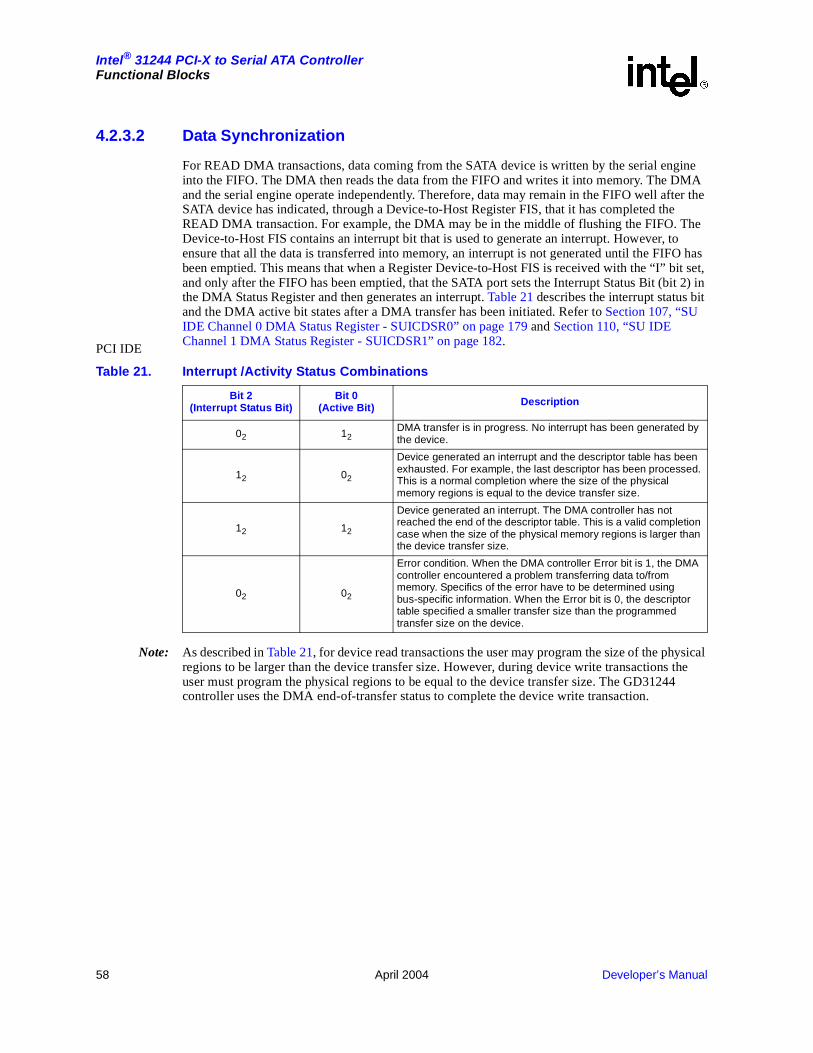
58 April 2004 Developer’s Manual
Intel® 31244 PCI-X to Serial ATA ControllerFunctional Blocks
4.2.3.2 Data Synchronization
For READ DMA transactions, data coming from the SATA device is written by the serial engine into the FIFO. The DMA then reads the data from the FIFO and writes it into memory. The DMA and the serial engine operate independently. Therefore, data may remain in the FIFO well after the SATA device has indicated, through a Device-to-Host Register FIS, that it has completed the READ DMA transaction. For example, the DMA may be in the middle of flushing the FIFO. The Device-to-Host FIS contains an interrupt bit that is used to generate an interrupt. However, to ensure that all the data is transferred into memory, an interrupt is not generated until the FIFO has been emptied. This means that when a Register Device-to-Host FIS is received with the “I” bit set, and only after the FIFO has been emptied, that the SATA port sets the Interrupt Status Bit (bit 2) in the DMA Status Register and then generates an interrupt. Table 21 describes the interrupt status bit and the DMA active bit states after a DMA transfer has been initiated. Refer to Section 107, “SU IDE Channel 0 DMA Status Register - SUICDSR0” on page 179 and Section 110, “SU IDE Channel 1 DMA Status Register - SUICDSR1” on page 182.
PCI IDE
Note: As described in Table 21, for device read transactions the user may program the size of the physical regions to be larger than the device transfer size. However, during device write transactions the user must program the physical regions to be equal to the device transfer size. The GD31244 controller uses the DMA end-of-transfer status to complete the device write transaction.
Table 21. Interrupt /Activity Status Combinations
Bit 2(Interrupt Status Bit)
Bit 0(Active Bit) Description
02 12DMA transfer is in progress. No interrupt has been generated by the device.
12 02
Device generated an interrupt and the descriptor table has been exhausted. For example, the last descriptor has been processed. This is a normal completion where the size of the physical memory regions is equal to the device transfer size.
12 12
Device generated an interrupt. The DMA controller has not reached the end of the descriptor table. This is a valid completion case when the size of the physical memory regions is larger than the device transfer size.
02 02
Error condition. When the DMA controller Error bit is 1, the DMA controller encountered a problem transferring data to/from memory. Specifics of the error have to be determined using bus-specific information. When the Error bit is 0, the descriptor table specified a smaller transfer size than the programmed transfer size on the device.

Developer’s Manual April 2004 59
Intel® 31244 PCI-X to Serial ATA ControllerFunctional Blocks
4.2.3.3 DMA Error Conditions
When during a DMA transfer, a bus master error condition is encountered like a master abort, target abort, or a parity error is detected, the SATA port DMA will stop the transfer by clearing the Active bit in the DMA Status register and setting the Error bit in the DMA Status register. Note that the SATA port does not generate an interrupt when a bus master operation is aborted. Software will time out. The following is a list of bus master errors that may be encountered during DMA transactions. Note that not all bus master error conditions result in the DMA stopping. Refer to Section 5.6, “PCI Bus Error Conditions” on page 83 for more details.
• Outbound Read Request Data Parity Errors
— Immediate Data Transfer
— Split Response Termination (PCI-X mode)
• Outbound Write Request Data Parity Errors
— Non-MSI Transactions (Message Signaled Interrupts
• Outbound Read Completion Address Parity Error
• Outbound Read Completions Attribute Parity Error
• Outbound Read Completion Data Parity Errors
• Split Completion Error Messages
• Master Abort for Outbound Read Requests
• Master Abort for Outbound Write Requests
• Target Abort for Outbound Read Requests
• Target ABort for Outbound Write Requests
When a requested device transfer (READ DMA or WRITE DMA) does not complete, the software driver will eventually time out. The software driver is then responsible for clearing the Start bit (bit 0) in the DMA Command register. Note that in this case the Error bit in the DMA Status register does not get set because there was no bus master error. An example of this type of error condition may occur when the DMA descriptors specified a smaller transfer size as the programmed transfer size in the device command. This causes the DMA to complete (DMA active bit cleared) while leaving the interrupt bit cleared. For example, an interrupt is not generated.

60 April 2004 Developer’s Manual
Intel® 31244 PCI-X to Serial ATA ControllerFunctional Blocks
4.2.3.4 DMA Throughput
The PCI bus efficiency is improved, by allowing large data packets to be transferred. The 31244 controller allows up to 512-byte packets per burst transfer on the PCI bus. Table 22 and Table 23 show the PCI-X bus efficiency, based on various packet sizes for read and write transactions respectively. The tables clearly indicate how, by transferring larger data packets, more bandwidth is available on the PCI-X bus.
In DPA Mode the 31244 controller provides one DMA engine per SATA port. Each SATA port also supports a 1 Kbyte FIFO. Each SATA port DMA operates independently and may transfer up to 512 bytes in one transfer.
To accommodate multiple DMA engines to operate concurrently, the 31244 controller employs an internal arbiter that controls the SATA ports DMA. The arbiter allows the DMAs to post requests in a round-robin fashion, thus providing a fair algorithm to the SATA ports.
Table 22. PCI-X Bus Efficiency for Reads
Read Transaction Size (Bytes)
PCI-X Data Cycles
Read Overhead Cycles (Split Reads)
Bus Efficiency
Available Bandwidth (MB/Sec)
66 MHz 100 MHz 133 MHz
64 8 11 42% 222 336 446
128 16 11 59% 311 472 627
256 32 11 74% 390 592 787
512 64 11 85% 435 680 904
1024 128 11 92% 485 736 978
Table 23. PCI-X Bus Efficiency for Writes
Write Transaction Size (Bytes)
PCI-X Data Cycles
Write Overhead Cycles
Bus Efficiency
Available Bandwidth (MB/Sec)
66 MHz 100MHz 133MHz
64 8 4 66% 348 528 702
128 16 4 80% 422 640 851
256 32 4 88% 464 704 936
512 64 4 94% 496 752 1000
1024 128 4 96% 506 768 1021
Figure 21. DMA Arbitration
A9375-01
PCI-XInterface
SATA Port 0 DMA
SATA Port 1 DMA
SATA Port 2 DMA
SATA Port 3 DMA
ARB

Developer’s Manual April 2004 61
Intel® 31244 PCI-X to Serial ATA ControllerFunctional Blocks
Table 24 and Table 25 provide the data transfer rate on the PCI-X bus, for a various number of ports, for read and write respectively. The transfer rates are based on 512-byte packets. Refer to Table 22 and Table 23 for PCI-X bandwidth numbers. Table 24 and Table 25 also show two 31244 controllers operating together, thus providing a total of eight ports. The numbers in Table 24 and Table 25 assume large sequential access across multiple drives.
Table 24. Read Transfer Rate on PCI-X Bus
Table 25. Write Transfer Rate on PCI-X Bus
Numberof Ports
PCI-XSpeed (MHz)
Transfer Rate (MB/Sec)
1 2 3 4 5 6 7 8
66 140 280 420 435 435 435 435 435
100 140 280 420 560 680 680 680 680
133 140 280 420 560 700 840 904 904
NOTE: The SATA transfer rate is 140MB/s, instead of 150MB/s in order to account for bus protocol overhead.
Numberof Ports
PCI-XSpeed (MHz)
Transfer Rate (MB/Sec)
1 2 3 4 5 6 7 8
66 140 280 420 496 496 496 496 496
100 140 280 420 560 700 752 752 752
133 140 280 420 560 700 840 1000 1000
NOTE: The SATA transfer rate is 140MB/s, instead of 150MB/s in order to account for bus protocol overhead.
62 April 2004 Developer’s Manual
Intel® 31244 PCI-X to Serial ATA ControllerFunctional Blocks
4.2.4 Programmed I/O (PIO)
PIO is an alternate way of transferring data instead of using the DMA Controller. Data is transferred by the host processor reading or writing the Data Port register of the Command Block. In the ATA standard, some commands may only use PIO to transfer data. For example, the IDENTIFY DEVICE command. During PIO reads, data is read from the Data Port register, essentially pulling data from the head of the receive FIFO, while the serial link is pushing incoming data from the serial link to the tail of the FIFO.
During PIO writes, data is pushed into the Data Port register. Data written to the Data Port register is placed at the tail of the speed matching transmit FIFO. The serial link pulls data to transmit from the head of the FIFO.
IDE devices are sector-based mass storage devices, which means that data is always transferred on sector boundaries, and therefore a sector is the smallest readable/writable unit. A sector count is specified as part of the ATA command issued to the device. The minimum sector count may be equal to one.
The ATA standard supports the following commands for PIO data transfers:
• READ SECTOR
• WRITE SECTOR
• READ MULTIPLE
• WRITE MULTIPLE
The READ SECTOR and READ MULTIPLE are used to read data from the device, whereas the WRITE SECTOR and WRITE MULTIPLE are used to write data to the device. The READ SECTOR and WRITE SECTOR commands allow data to be transferred one sector per interrupt. For example, during a READ SECTOR command, an interrupt is generated by the device to indicate that a sector of data is ready to be read. After the sector is read, a new interrupt is generated when the next sector is ready to be transferred and this process continues until the requested sector count is exhausted. The WRITE SECTOR command also is used to transfer one sector per interrupt. The READ MULTIPLE and WRITE MULTIPLE commands allow multiple sectors to be transferred per interrupt instead of one sector per interrupt like the READ SECTOR and WRITE SECTOR commands. Most IDE devices support this feature and provide a programmable register on the device, which the user may program using the SET FEATURES command to setup the desired number of sectors to transfer per interrupt.
In both conventional PCI and PCI-X mode, during PIO transfers the GD31244 controller will respond with a retry when data is not available in the FIFO during reads or when the FIFO is full during writes.
The SATA Unit may be set up during system reset to execute in one of the following modes. Each mode provides a different programming interface. The DPA_MODE# external strap signal is sampled during the rising edge of PCI reset, to determine the operation mode.
• PCI IDE Mode
• PCI Direct Port Access Mode

Developer’s Manual April 2004 63
Intel® 31244 PCI-X to Serial ATA ControllerFunctional Blocks
4.2.5 Serial ATA II Native Command Queuing
Serial ATA II Command Queuing enables a hard drive to accept multiple commands from the GD31244 controller and rearrange the completion order of those commands to maximize throughput. The major portion of the drive’s command service time is seek and rotational delay for the drive head to land on the appropriate data to transfer. The drive can use rotational optimizations to select the next command to complete such that the major components of the service time, seek and rotational delay, are minimized. A major advantage to command queuing is that the command issue and completion overhead may be overlapped with the drive seek and rotational delay for a different command's data transfer. For example, while a new command is being issued to the drive, the drive may be seeking to locate the appropriate track on disk for data for a different command. In essence, the latency for issuing the new command is saved since it was overlapped with the seek for another command.
Serial ATA II Native Command Queuing provides an efficient and streamlined data transfer and status return mechanism. This performance and efficiency is achieved through features of the SATA II Native Command Queuing protocol that include race-free status return mechanism, interrupt aggregation, and First Party DMA.

64 April 2004 Developer’s Manual
Intel® 31244 PCI-X to Serial ATA ControllerFunctional Blocks
4.2.5.1 Race-free Status Return Mechanism
Serial ATA II Native Command Queuing has a race-free status return mechanism that allows status to be returned on any command at any time. There is no handshake required with the host for the status return. The drive may issue command completions for multiple commands back-to-back or even at the same time.
The Serial ATA II Native Queuing definition utilizes the reserved 32-bit field in the Set Device Bits FIS to convey the pending status for each of up to 32 outstanding commands. The BSY bit in the Status register conveys only the device’s readiness to receive another command, and does not convey the completion status of queued commands. The 32 reserved bits in the Set Device Bits FIS are handled as a 32-element array of active command bits (referred to as ACT bits), one for each possible outstanding command, and the array is bit significant such that bit “n” in the array corresponds to the pending status of the command with tag “n.”
The SActive register is used to track completion status of queued commands. This register is part of the control, status and error superset registers defined in the Serial ATA specification. In GD31244 this register is known as the Set Device Bits FIS Register SUPDSDBR.
Before host driver software issues a queued command to the device, it sets the bit corresponding to the tag of the queued command it is about to issue. When the device completes a queued command, it clears the bit corresponding to the tag of the queued command in the SActive bits in the Set Device Bits FIS. When the GD31244 receives the Set Device Bits FIS from the device it will automatically clears the bit corresponding to the tag of the queued command in the Set Device Bits FIS Register SUPDSDBR (SActive register). Host driver software queries the SActive register to determine which commands are complete.
This mechanism of the host controller setting bits in the register and the device clearing bits in the register ensures that no race condition can occur.
These examples describe how the bit field relates to the status of queued commands:
• 1 in bit location 0 signifies that the command with tag 0 is still pending
• 1 in bit location 16 signifies that the command with tag 16 is still pending
• 0 in bit location 16 signifies that the command with tag 16 is complete (if the bit was previously set)
4.2.5.2 Interrupt Aggregation
Serial ATA II Native Command Queuing has a maximum of one interrupt per command. In actuality, the number of interrupts per command is less than one due to a feature called interrupt aggregation. If the drive completes multiple commands in a short time span, the individual interrupts for each command may be aggregated into one interrupt by the GD31244. In this case, the host software driver only sees one interrupt for multiple commands. In a highly queued workload this is a frequent occurrence since host software interrupt service latency may be long in comparison to the time between command completions.

Developer’s Manual April 2004 65
Intel® 31244 PCI-X to Serial ATA ControllerFunctional Blocks
4.2.5.3 First Party DMA (FPDMA)
Serial ATA II Native Command Queuing has a mechanism such that the drive can select the DMA context for a subsequent data transfer without host software intervention using the GD31244. This mechanism is called First Party DMA. The drive selects the DMA context by sending a DMA Setup FIS to the host controller specifying the tag of the command that the data transfer is for. The host controller will load the scatter/gather table pointer for that command (based on the tag value) into the DMA engine. Then the DMA transfer may proceed.
The Serial ATA II Native Queuing definition utilizes the reserved 32-bit field in the Set Device Bits FIS to convey the pending status for each of up to 32 outstanding commands. The BSY bit in the Status register conveys only the device’s readiness to receive another command, and does not convey the completion status of queued commands. The 32 reserved bits in the Set Device Bits FIS are handled as a 32-element array of active command bits (referred to as ACT bits), one for each possible outstanding command, and the array is bit significant such that bit “n” in the array corresponds to the pending status of the command with tag “n.”
Data returned by the device (or transferred to the device) for queued commands use the First Party DMA mechanism to cause the host controller to select the appropriate destination/source memory buffer for the transfer. The memory handle used for the buffer selection is the same as the tag that is associated with the command. For traditional desktop host controllers, the handle may be used to index into a vector of pointers to pre-constructed scatter/gather lists (often referred to as physical region descriptor tables or simply PRD tables) in order to establish the proper context in the host’s DMA engine.
Status is returned by updating the 32-element bit array in the Set Device Bits FIS for successful completions. For failed commands, the device halts processing commands allowing host software or controller firmware to intervene and resolve the source of the failure before processing is again explicitly restarted. For more information on native command queueing, see Serial ATA II: Extensions to Serial ATA 1.0
66 April 2004 Developer’s Manual
Intel® 31244 PCI-X to Serial ATA ControllerProgramming Interface
Programming Interface 5
The GD31244 register set is composed of several functional groups, some of which appear at different addresses and in different spaces (configuration, I/O, memory) when used in PCI IDE mode or DPA mode. PCI IDE mode is a legacy mode that uses I/O space for backwards compatibility while DPA mode is a new design using memory space. In PCI IDE mode, PCI ATA specifications use 5 of the 6 available BAR windows for task file and DMA registers. The Superset registers use the last BAR (BAR5). All other registers use configuration space.
Besides the required PCI configuration register set, these include:
• the PCI/PCI-X core configuration
• the Serial Expansion ROM registers
• the common port registers
• assorted control registers
In DPA mode, all the (I/O space) registers to which the 6 BAR registers point are consolidated into a single contiguous (memory space) set of registers to which BAR0/1 points. In addition, several of the common port registers are moved from the PCI configuration space to the BAR0/1 defined space. As defined in the PCI Local Bus Specification, BAR0/1 are used to allow for a 64-bit memory address with BAR0 being the low order 32 bits and BAR1 being the high order 32 bits of the address. The GD31244 uses mode pin MS_DA to place the device in Master/Slave mode (when HIGH) or DPA mode (when LOW). This determination is made at power up so I/O and Memory can be configured correctly.

Developer’s Manual April 2004 67
Intel® 31244 PCI-X to Serial ATA ControllerProgramming Interface
5.1 PCI IDE Mode
The SATA Unit supports both Native-PCI IDE modes. In this mode, the GD31244 conforms to the PCI IDE Specification - Revision 1.0. In PCI IDE mode, the following registers are available to the user and are mapped in the I/O space.
• Command Block Registers
• Control Block Registers
• DMA Registers
5.1.1 Native-PCI Mode
In Native-PCI IDE mode, the Command Block Registers and Control Block Registers are completely relocatable in the I/O space using the PCI Base Address Registers, Section 5.10.2.11, “SU Base Address Register 0 - SUBAR0” on page 119, Section 5.10.2.12, “SU Base Address Register 1 - SUBAR1” on page 120, Section 5.10.2.13, “SU Base Address Register 2 - SUBAR2” on page 121, and Section 5.10.2.14, “SU Base Address Register 3 - SUBAR3” on page 122. Table 26 shows the Base Address Registers and how they are used.
Table 26. SATA Port Register Mapping in Native PCI IDE Mode
Configuration Space BAR Offset Registers
10H Primary Channel Command Block
14H Primary Channel Control Block
18H Secondary Channel Command Block
1CH Secondary Channel Control Block
20H Primary and Secondary Channel DMA Registers
24H SATA Superset Registers

68 April 2004 Developer’s Manual
Intel® 31244 PCI-X to Serial ATA ControllerProgramming Interface
Figure 22 shows how the SATA port registers are mapped in native-PCI IDE mode. Note that the DMA Controller Registers for both channels are accessed using the Base Address Register at offset 20H.
Figure 22. SATA Unit Register Mapping in Native-PCI Mode
DMA Registers
Command Block Registers
Control Bock Registers
Channel 0
Channel 1
Channel 0 & Channel 1
Base Address Register 0Base Address Register 1
Base Address Register 2Base Address Register 3
Base Address Register 4
Base Address Register 5
PCI Configuration Space
10H14H18H1CH20H
Offset
24H
Command Block Registers
Control Bock Registers
SATA Superset Registers

Developer’s Manual April 2004 69
Intel® 31244 PCI-X to Serial ATA ControllerProgramming Interface
5.2 Direct Port Access Mode
This mode is specific to the 31244, it allows an external PCI master to control each SATA port independently. All four SATA port registers within the Serial ATA Unit are mapped contiguously in the PCI Memory Space using the PCI Base Address Registers, Section 5.10.7.1, “SU PCI DPA Base Address Register 0 - SUPDBAR0” on page 192 and Section 5.10.7.2, “SU PCI DPA Upper Base Address Register 0 - SUPDUBAR0” on page 193. Each SATA port register occupies 512 bytes of space. Figure 23 shows the SATA ports to Base Address Register mapping. All the four SATA port registers within a Serial ATA Unit occupy 4 Kbytes of space. There is a common set of registers that are shared by all the SATA ports. Each SATA port consists of the following register blocks. The SATA ports registers are offset at 200H, 400H, 600H, and 800H for SATA Port 0, 1, 2, and 3 respectively. The Command Port register space starts at offset 000H.
• Common SATA Port Registers - shared by all SATA ports
• Command Block Registers
• Control Block Registers
• DMA registers
• Superset Registers
Figure 23. SATA Unit Register Mapping in Direct Port Access Mode
SATA Port 0 Registers
0
200H
3FFH400H
5FFH600H
7FFH800H
SATA Port 3 Registers
9FFH
SATA Port 1 Registers
Offset
SATA Port 2 Registers
Common Port Registers1FFH
2 Kbytes
512 Bytes
(4 x 512 Bytes)
PCI Configuration Space
10H
14H
Offset
Base Address Register
Upper Base Address Register 0
31
000H
A00H
FFFH
1536 BytesReserved

70 April 2004 Developer’s Manual
Intel® 31244 PCI-X to Serial ATA ControllerProgramming Interface
5.2.1 Common Serial ATA Port Registers
This section defines the registers that are common to all the Serial ATA ports for the SATA Unit. Figure 24 shows the registers mapping.
5.2.2 Command Block Registers
The Command Block Registers are used to issue ATA commands to the device. The Command Register must be written after the other registers in the Command Block are loaded, because the rest of the registers are parameters based on the command. The structure of the command block is shown in Figure 25. The Command Block Registers are memory-mapped when in the Direct Port Access mode. When in the PCI IDE mode, the Command Block Registers are I/O-mapped in the PCI I/O space. Figure 25 shows the Command Block Registers mapping when in the Direct Port Access mode (DPA) for SATA Port 0. Refer to Section , “The SATA Unit may be set up during system reset to execute in one of the following modes. Each mode provides a different programming interface. The DPA_MODE# external strap signal is sampled during the rising edge of PCI reset, to determine the operation mode.” on page 62 for further details on the mapping of these registers.
Figure 24. Common Serial ATA Port Registers
031 Offset
008H - 1FFH Reserved
004H
Serial ATA Unit Interrupt Pending Register 000H
Serial ATA Unit Interrupt Mask Register
Figure 25. Command Block Registers for SATA Port 0
Cylinder Low Register
Sector Count Register
Device/Head Register
Cylinder High Register
Sector Number Register
204H
200H
208H
20CH
210H
214H
218H
21CH
031
Command/Status Register
Offset
Features/Error Register
Data Port Register

Developer’s Manual April 2004 71
Intel® 31244 PCI-X to Serial ATA ControllerProgramming Interface
5.2.3 Control Block Registers
The Control Block Registers provide control and status of the device. Figure 26 shows the Control Block Register mapping. Refer to Section , “The SATA Unit may be set up during system reset to execute in one of the following modes. Each mode provides a different programming interface. The DPA_MODE# external strap signal is sampled during the rising edge of PCI reset, to determine the operation mode.” on page 62 for further details on the mapping when in the Direct Port Access mode (DPA) of the registers for SATA Port 0.
5.2.4 DMA Controller Registers
The DMA Controller Registers provide control and status for the DMA Controller. Several ATA commands use the DMA Controller to transfer data between device and memory. Figure 27 shows the DMA Controller register mapping when in the Direct Port Access mode (DPA) for SATA Port 0. Refer to Section , “The SATA Unit may be set up during system reset to execute in one of the following modes. Each mode provides a different programming interface. The DPA_MODE# external strap signal is sampled during the rising edge of PCI reset, to determine the operation mode.” on page 62 for further details on the mapping of the registers.
Figure 26. Control Block Registers for SATA Port 0
224H
220H
22CH
031Offset
Reserved
Reserved
Reserved
228H Device Control/Alternate Status Registers
Figure 27. DMA Controller Registers for SATA Port 0
031 Offset
DMA Command/Status Registers
DMA Descriptor Table Pointer
270H
274H
DMA Control Register 260H
DMA Upper Descriptor Table Pointer 264H
DMA Upper Data Buffer Pointer 268H
Reserved 26CH - 26FH
72 April 2004 Developer’s Manual
Intel® 31244 PCI-X to Serial ATA ControllerProgramming Interface
5.2.5 SATA Superset Registers
The SATA Superset Registers, define two sets of registers. These registers are specific to the Serial ATA Specification, hence superset.
The Serial ATA Specification defines an additional block of registers mapped separately and independently from the ATA Command Block Registers for additional status and error information and allow control of capabilities unique to Serial ATA. These registers referred to as the Serial ATA Status and Control Registers (SCRs) are organized as 16 contiguous 32-bit registers. The current specification defines three registers only, and the remaining thirteen are reserved for future implementation. The defined SCRs are as follows:
• SStatus Register
• SError Register
• SControl Register
The Serial ATA protocol also provides additional SATA specific commands. The Serial ATA defines two Frame Information Structures (FIS) that are not used by the current ATA Command set. However, these FISs may be used to enable new device capabilities.
• BIST Activate (Bidirectional)
• DMA Setup - Device to Host or Host to Device (Bidirectional)
Table 27 shows the SATA Interface Registers mapping when in the Direct Port Access mode for SATA Port 0. Refer to Section , “The SATA Unit may be set up during system reset to execute in one of the following modes. Each mode provides a different programming interface. The DPA_MODE# external strap signal is sampled during the rising edge of PCI reset, to determine the operation mode.” on page 62 for further details on the mapping of the registers based on the specific programming interface. When in PCI IDE mode, the super registers of a device on a given channel are selected using the DEV bit of the Device/Head register (bit 4). A channel (primary or secondary) is selected using bit 16 of the APT Control Register. Refer to Section 5.10.3.8, “SU IDE Device/Head Register - SUIDR” on page 173 and Section 5.10.2.30, “SU Extended Control and Status Register 0 - SUECSR0” on page 138. Also, when in PCI IDE mode, the superset registers are accessed using Base Address Register 5. Refer to Section 5.10.2.16, “SU Base Address Register 5 - SUBAR5” on page 124.
Note: The superset registers when in PCI IDE mode are accessed using SUBAR5 starting at offset 000H. For example, Table 27 shows the first register starting at offset 300H, 304H, 308H and so on in DPA mode. In PCI IDE mode, the registers start at offset 00H, 004H, 008H and so on.
Developer’s Manual April 2004 73
Intel® 31244 PCI-X to Serial ATA ControllerProgramming Interface
Table 27. SATA Superset Registers for SATA Port 0 in DPA Mode
31 0 Offset
SCRs Registers
SU PCI DPA SATA SStatus Register - SUPDSSSR 300H
SU PCI DPA SATA SError Register - SUPDSSER 304H
SU PCI DPA SATA SControl Register - SUPDSSCR 308H
SU PCI DPA Set Device Bits Register - SUPDSDBR 30CH
Reserved 310H - 33FH
SU PCI DPA PHY Feature Register - SUPDPFR 340H
BIST Registers
SU PCI DPA BIST FIS Control and Status Register - SUPDBFCSR 344H
SU PCI DPA BIST Errors Register - SUPDBER 348H
SU PCI DPA BIST Frames Register - SUPDBFR 34CH
SU PCI DPA Host BIST Data Low Register - SUPDHBDLR 350H
SU PCI DPA Host BIST Data High Register - SUPDHBDHR 354H
SU PCI DPA Device BIST Data Low Register - SUPDDBDLR 358H
SU PCI DPA Device BIST Data High Register - SUPDDBDHR 35CH
DMA Setup Registers
SU PCI DPA Queuing Table Address Register Low - SUPDQTBARL 360H
SU PCI DPA Queuing Table Address Register High - SUPDQTBARH 364H
SU PCI DPA DMA Setup FIS Control and Status Register - SUPDDSFCSR 368H
SU PCI DPA Host DMA Buffer Identifier Low Register - SUPDHDBILR 36CH
SU PCI DPA Host DMA Buffer Identifier High Register - SUPDHDBIHR 370H
SU PCI DPA Host Reserved DWORD Register 0 - SUPDHRDR0 374H
SU PCI DPA Host DMA Buffer Offset Register - SUPDHDBOR 378H
SU PCI DPA Host DMA Transfer Count Register - SUPDHDTCR 37CH
SU PCI DPA Host Reserved DWORD Register 1- SUPDHRDR1 380H
SU PCI DPA Device DMA Buffer Identifier Low Register - SUPDDDBILR 384H
SU PCI DPA Device DMA Buffer Identifier High Register - SUPDDDBIHR 388H
SU PCI DPA Host Reserved DWORD Register 0 - SUPDHRDR0 38CH
SU PCI DPA Device DMA Buffer Offset Register - SUPDDDBOR 390H
SU PCI DPA Device DMA Transfer Count Register - SUPDDDTCR 394H
SU PCI DPA Device Reserved DWORD Register 1 - SUPDDRDR1 398H
Reserved Route
Reserved 39CH
Reserved 3A0H
Reserved 3A4H
Reserved 3A8H
Reserved 3ACH
Reserved 3B0H
Reserved 3B4H
Reserved 3B8H
Reserved 3BCH
Reserved 3C0H
Reserved 3C4H
Reserved 3C8H
Test Register 0 3CCH
Test Register 1 3D0H
Reserved 3D4H - 3FFH
NOTE: The Offsets mentioned above, only indicate Port 0. To view the other three Port offset values, see each specific register.
74 April 2004 Developer’s Manual
Intel® 31244 PCI-X to Serial ATA ControllerProgramming Interface
5.3 ATA Command Processing
A command is issued to a device by writing the Command Block Registers. The command register should be written last, after the rest of the registers are written. The rest of the registers, except for the data port register, are parameters based on the command. Writing the command register initiates a transfer of a Register FIS from the controller to the device.
Commands may be categorized as data and non-data commands. Non-data commands do not involve data transfer. Examples of such commands are:
Refer to the AT Attachment with Packet Interface-6 (ATA/ATAPI-6) Specification. Data commands involve the transfer of one or more blocks of data. There are two classes of data commands. There are data commands that use the DMA protocol to transfer data and others that use the PIO protocol. Examples of PIO data commands are:
Examples of DMA data commands are:
• READ DMA
• WRITE DMA
For PIO commands, data is transferred by either reading or writing the Command Block Data Port Register.
An ATA device is addressed by using two methods:
CHS Cylinder/Head/Sector.
LBA Logical Block Addressing.
Disk assembly of a drive usually consists of a number of surfaces, each of which stores data on concentric circles called tracks. The tracks are further divided into sectors, which are the smallest readable/writable units. A sector is accessed by first positioning the read/write head above the proper track and then waits until the desired sector rotates underneath the head to read or write the data. Writing and reading the sector is done serially bit-by-bit.
A drive usually contains multiple disks, and both sides of the a disk may be utilized for storage. Each surface has its own read/write head although only one track may be written to or read at a given time. The heads are positioned collectively over the tracks. A set of tracks that may be accessed by the heads from a single position is a cylinder. A consequence of this organization is that every sector may be addressed by its Cylinder, Head, and Sector Numbers. This is referred to as the drive geometry.
In LBA mode, the drive presents itself as a continuous sequence of sectors or blocks which are addressed by their logical block number, like 0, 1, 2,...N-1, where N is the number of sectors on the drive. In this case the drive physical geometry (CHS) need not be known to the host. For example, the drive presents itself more or less like random memories are presented where an address is used to select a byte from an array of bytes, thus the actual topology of the memory bits need not be known by the user.
• SEEK • IDLE • SLEEP
• NOP • FLUSH CACHE • STANDBY
• READ BUFFER • WRITE BUFFER
• READ SECTOR • WRITE SECTOR

Developer’s Manual April 2004 75
Intel® 31244 PCI-X to Serial ATA ControllerProgramming Interface
5.3.1 LBA Addressing in PCI IDE Mode
This section describes how the command block registers are utilized in 28-bit and 48-bit LBA addressing modes. The Device/Head register (bit 6) indicates whether a command is using CHS (Cylinder/Head/Sector) or LBA address format. When bit 6 of the Device/Head register is set, LBA address format is being used. Table 28 shows how the command block registers are utilized for 28-bit LBA addressing.
Table 29 shows how the command block registers are utilized for 48-bit LBA addressing. To preserve the same ATA standard programming interface, the Sector Count, LBA Low, LBA Mid, and LBA High registers are kept as 8-bit registers. Instead, these registers are implemented as 8-bit ports to two-byte deep FIFOs. Note that the 8-bit port must always be written in pairs, otherwise proper functionality is not guaranteed. For example, a 16-bit value is loaded to any of these registers by performing two 8-bit writes. The three 16-bit registers, therefore, provides the 48-bit LBA address bits. The most recently written value to any of these registers is pushed into the lower byte position and the previous written value gets pushed into the upper byte position. As an example, when the value 17H is written to Cylinder Low/LBA Mid register followed by the value 68H to the same register, the value 17H first goes into LBA[15:8]. After the value 68H is written, the value 17H gets pushed into LBA[39:32] and the value 68H goes into LBA[15:8]. Table 30 summarizes the loading sequence.
Note: Note that the Device/Head register is not used to form a 48-bit LBA address. However, bits 0-3 of the Device/Head register must be set high.
Table 28. 28-Bit LBA Address Bit Layout in PCI IDE Mode
LBA Bits
Register
Register Bit Location
7 6 5 4 3 2 1 0
Sector Number / LBA Low 7 6 5 4 3 2 1 0
Cylinder Low / LBA Mid 15 14 13 12 11 10 9 8
Cylinder High / LBA High 23 22 21 20 19 18 17 16
Device/Head N/A LBA N/A DEV 27 26 25 24
Table 29. 48-Bit LBA Address Bit Layout
Table 30. 48-Bit Address Loading Sequence
Register Most Recently Written Previous Content
Sector Count Sector Count[7:0] Sector Count[15:8]
Sector Number / LBA Low LBA[7:0] LBA[31:24]
Cylinder Low / LBA Mid LBA[15:8] LBA[39:32]
Cylinder High / LBA High LBA[23:16] LBA[47:40]
LBA Bits
Register
Register Bit Location
7 6 5 4 3 2 1 0
Sector Number / LBA Low 31/7 30/6 29/5 28/4 27/3 26/2 25/1 24/0
Cylinder Low / LBA Mid 39/15 38/14 37/13 36/12 35/11 34/10 33/9 32/8
Cylinder High / LBA High 47/23 46/22 45/21 44/20 43/19 42/18 41/17 40/16
Device/Head N/A LBA N/A DEV 1 1 1 1

76 April 2004 Developer’s Manual
Intel® 31244 PCI-X to Serial ATA ControllerProgramming Interface
5.3.2 LBA Addressing in DPA Mode
In DPA mode, the Sector Count, Sector Number, Cylinder Low, Cylinder High registers are 16-bit wide. Therefore, the Sector Count and the LBA address bits may be written simultaneously.
Table 31. 28-Bit LBA Address Bit Layout in DPA Mode
Table 32. 48-Bit LBA Address Bit Layout in DPA Mode
LBA Bits
Register
Register Bit Location
7 6 5 4 3 2 1 0
Sector Number / LBA Low 7 6 5 4 3 2 1 0
Cylinder Low / LBA Mid 15 14 13 12 11 10 9 8
Cylinder High / LBA High 23 22 21 20 19 18 17 16
Device/Head N/A LBA N/A N/A 27 26 25 24
LBA Bits
Register
Register Bit Location
15 14 13 12 11 10 9 8 7 6 5 4 3 2 1 0
Sector Number / LBA Low 31 30 29 28 27 26 25 24 7 6 5 4 3 2 1 0
Cylinder Low / LBA Mid 39 38 37 36 35 34 33 32 15 14 13 12 11 10 9 8
Cylinder High / LBA High 47 46 45 44 43 42 41 40 23 22 21 20 19 18 17 16
Device/Head N/A LBA N/A N/A 1 1 1 1

Developer’s Manual April 2004 77
Intel® 31244 PCI-X to Serial ATA ControllerProgramming Interface
5.4 Reset Initialization
When the PCI bus reset signal P_RST# is asserted, the GD31244 controller:
• resets all internal units
• resets all the registers to their default values
• latches the configuration strap on the rising edge of P_RST#.
• latches P_REQ64# to determine the PCI bus width
• initiates a COMRESET/hardware reset to the SATA devices on the rising edge of P_RST#. Note that COMRESET is initiated only when in PCI IDE mode. When in DPA mode, COMRESET have to be explicitly initiated using the SControl Register by software. Refer to the DET field in the “SU PCI DPA SATA SControl Register - SUPDSSCR” on page 225.
All the state machines on the GD31244 controller get reset upon the assertion of the PCI bus signal P_RST#. In addition, all the registers on the GD31244 controller get initialized to their default values.
Upon the deassertion of P_RST#, the GD31244 controller samples the DPA_MODE# strap pin to set the operating mode. When DPA_MODE# is high after reset is deasserted, the GD31244 controller will present itself on the PCI bus as a PCI IDE device (Default Mode). When DPA_MODE# is low after reset, the GD31244 controller will present itself on the PCI bus in DPA (Direct Port Access) mode (requires a pull-down resistor).
The P_REQ64# signal is also sampled to determine when the GD31244 controller is connected on a 64-bit PCI bus. P_REQ64# is latched on the rising edge of P_RST#. The state of P_REQ64# at the rising edge of P_RST# notifies the GD31244 controller that it is connected to a 64-bit or 32-bit PCI bus.
The 32BITPCI# is also sampled to indicate the width of the PCI-X bus to the PCI-X Status Register. When 32BITPCI# is low after reset is deasserted, it implies a 32-bit PCI-X Bus (requires pull-down resistor). When 32BITPCI# high after reset is deasserted, it implies a 64-bit PCI-X Bus (Default mode)
A COMRESET is used to hardware reset the SATA device and also to initialize the serial bus communication link. A COMRESET is issued differently in PCI mode and DPA mode. In PCI IDE mode, upon the deassertion of P_RST#, a COMRESET is issued to each SATA drive. In DPA mode, the serial bus will stay offline after P_RST# is deasserted. Software must intervene in order to initiate a COMRESET initialization sequence using the SControl register. Refer to the “SU PCI DPA SATA SControl Register - SUPDSSCR” on page 225. This is done in order to minimize an initial power supply current draw due to multiple spindles starting at once.
A COMRESET sequence causes a hardware reset of the SATA device and initialization of the serial bus communication link. Because of the nature of the Serial ATA bus, before the SATA port may communicate to the attached SATA device, an initialization sequence is required to establish the communication link. The PHY internally provides a mechanism (PHY Ready) to indicate that a device is present. Until a device is not detected the Command Block Status register returns a 7FH value when read. This value is consistent with ATA standard devices, which indicates that a device is not connected and therefore, software should not try writing to the taskfile registers. After the device is detected, the Status register returns an 80H value. Bit 7 set (BSY bit) indicates that a device is present but is busy performing its initialization sequence. After the device completes its initialization sequence, it will send a Register FIS to initialize the taskfile registers. The values returned in the Register FIS are device dependent, and provide the status of the drive. The Error register contains a diagnostic code. The Sector Count, Sector Number, Cylinder Low, Cylinder High and Device/Head

78 April 2004 Developer’s Manual
Intel® 31244 PCI-X to Serial ATA ControllerProgramming Interface
registers contain signatures that are device dependent. Refer to the AT Attachment with Packet Interface-6 (ATA/ATAPI-6) Specification for more details regarding the values returned in the Device-to-Host Register FIS.
A COMRESET may also be initiated by software writing the DET field of the SControl register.
A software reset is initiated by writing a one to the SRST bit (bit 2) (software reset bit) of the Device Control register. A software reset simply initiates a device reset, and does not initiate any serial link initialization sequence as described above based on a COMRESET. After a software reset, the device will send a Device-to-Host Register FIS. The values returned in the Register FIS are device-dependent, and provide information as far as the status of the drive. The Error register contains a diagnostic code. The Sector Count, Sector Number, Cylinder Low, Cylinder High and Device/Head registers contain signatures that are device dependent. Refer to the AT Attachment with Packet Interface-6 (ATA/ATAPI-6) Specification for more details regarding the values returned in the Device-to-Host Register FIS.
Devices that implement the packet command set may also be reset using the DEVICE RESET command. This command may be issued to an individual device using the DEV bit without affecting the other device. After the device is reset, it will return a Device-to-Host Register FIS. The Error register contains a diagnostic code. The Sector Count, Sector Number, Cylinder Low, Cylinder High and Device/Head registers contain signatures that are device dependent. Refer to the AT Attachment with Packet Interface-6 (ATA/ATAPI-6) Specification for more details regarding the values returned in the Device-to-Host Register FIS.
The EXECUTE DEVICE DIAGNOSTIC command may be used to initiate a device diagnostic. After the device completes its diagnostic sequence, it will return a Device-to-Host Register FIS. The Error register contains a diagnostic code. The Sector Count, Sector Number, Cylinder Low, Cylinder High and Device/Head registers contain signatures that are device dependent. Refer to the AT Attachment with Packet Interface-6 (ATA/ATAPI-6) Specification for more details regarding the values returned in the Device-to-Host Register FIS.
Note: In a Master/Slave setup, the GD31244 controller will merge the contents of the taskfile Error and Status register values from the attached devices, in accordance with the ATA standard, to produce the Error and Status register values visible to host software. Refer to the AT Attachment with Packet Interface-6 (ATA/ATAPI-6) Specification for details.
Note: In a Master/Slave setup, a hardware reset, a software reset, and an EXECUTE DEVICE DIAGNOSTIC command will cause both master and slave devices to perform the requested task simultaneously. However, a DEVICE RESET command may be targeted at only one device at a time using the DEV bit in the Device/Head register.
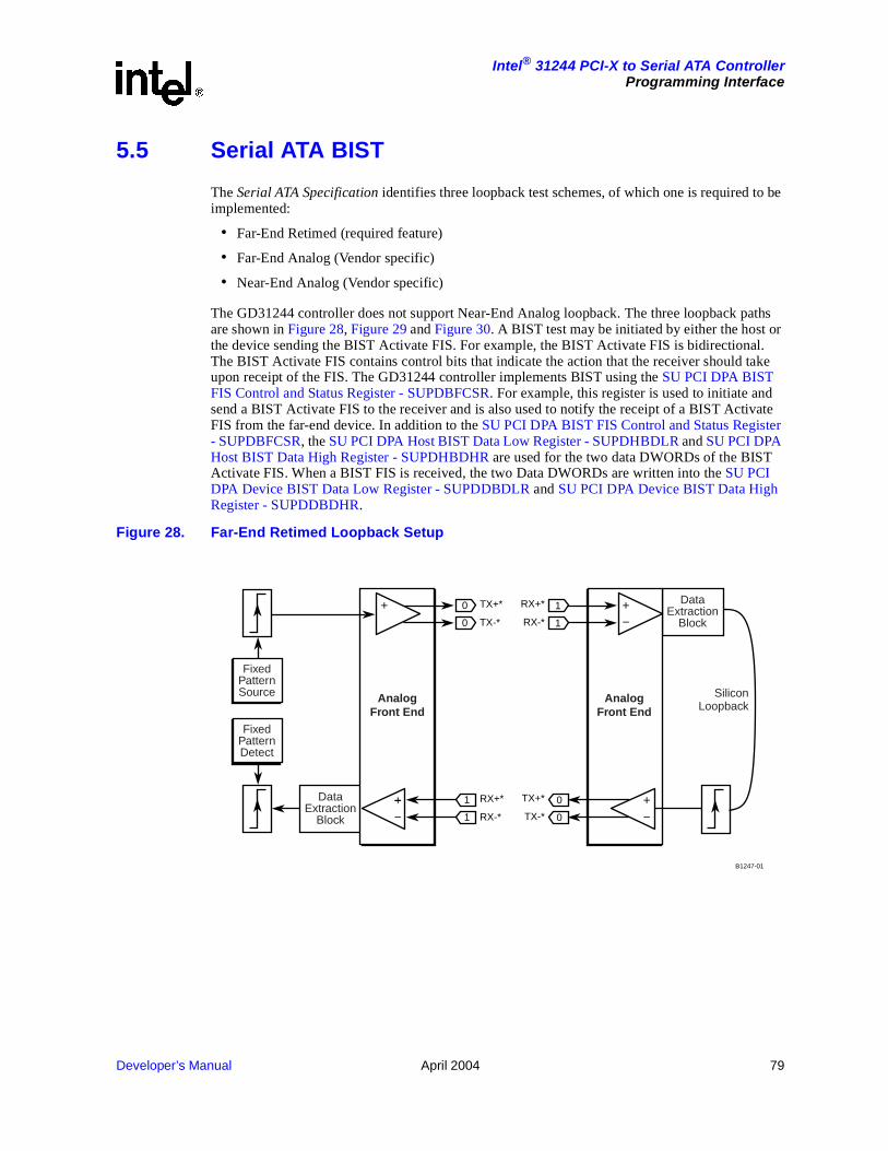
Developer’s Manual April 2004 79
Intel® 31244 PCI-X to Serial ATA ControllerProgramming Interface
5.5 Serial ATA BIST
The Serial ATA Specification identifies three loopback test schemes, of which one is required to be implemented:
• Far-End Retimed (required feature)
• Far-End Analog (Vendor specific)
• Near-End Analog (Vendor specific)
The GD31244 controller does not support Near-End Analog loopback. The three loopback paths are shown in Figure 28, Figure 29 and Figure 30. A BIST test may be initiated by either the host or the device sending the BIST Activate FIS. For example, the BIST Activate FIS is bidirectional. The BIST Activate FIS contains control bits that indicate the action that the receiver should take upon receipt of the FIS. The GD31244 controller implements BIST using the SU PCI DPA BIST FIS Control and Status Register - SUPDBFCSR. For example, this register is used to initiate and send a BIST Activate FIS to the receiver and is also used to notify the receipt of a BIST Activate FIS from the far-end device. In addition to the SU PCI DPA BIST FIS Control and Status Register - SUPDBFCSR, the SU PCI DPA Host BIST Data Low Register - SUPDHBDLR and SU PCI DPA Host BIST Data High Register - SUPDHBDHR are used for the two data DWORDs of the BIST Activate FIS. When a BIST FIS is received, the two Data DWORDs are written into the SU PCI DPA Device BIST Data Low Register - SUPDDBDLR and SU PCI DPA Device BIST Data High Register - SUPDDBDHR.
Figure 28. Far-End Retimed Loopback Setup
B1247-01
AnalogFront End
DataExtraction
Block
SiliconLoopback
RX+*
RX-*
1
1
TX+*
TX-*
0
0
AnalogFront End
DataExtraction
Block
FixedPatternDetect
RX+*
RX-*
0
0
TX+*
TX-*
1
FixedPatternSource
1

80 April 2004 Developer’s Manual
Intel® 31244 PCI-X to Serial ATA ControllerProgramming Interface
Figure 29. Far-End Analog Loopback Setup
Figure 30. Near-End Analog Loopback Setup
B1249-01
AnalogFront End
DataExtraction
Block
RX+*
RX-*
1
1
TX+*
TX-*
0
0
AnalogFront End
DataExtraction
Block
FixedPatternDetect
RX+*
RX-*
0
0
TX+*
TX-*
1
FixedPatternSource
1
SiliconLoopback
B1250-01
AnalogFront End
DataExtraction
Block
RX+*
RX-*
1
1
TX+*
TX-*
0
0
AnalogFront End
DataExtraction
Block
FixedPatternDetect
RX+*
RX-*
0
0
TX+*
TX-*
1
FixedPatternSource
1
SiliconLoopback
Developer’s Manual April 2004 81
Intel® 31244 PCI-X to Serial ATA ControllerProgramming Interface
5.5.1 Loopback Mode Testing
In the loopback modes (Far-End Retimed or Far-End Analog), the GD31244 controller may be programmed to generate one of four BIST patterns:
• 002 - D2.5s
• 012 - D24.3s
• 102 - 3(D10.2s) and K28.5
• 112 - 16-bit counting pattern
A BIST pattern is selected by programming bits [31:30] of the SU PCI DPA BIST FIS Control and Status Register - SUPDBFCSR. Programming bits [31:30] with 002 will generate a stream of D2.5 data characters. Programming bits [31:30] with 012 will generate a stream of D24.3 data characters. Programming bits [31:30] with 102 will generate a stream of three D10.2 data and one K28.5 control characters. Programming bits [31:30] with 112 will generate a 16-bit counting pattern. The counting pattern is a sequence of 65536 DWORDs, repeated indefinitely until the test is concluded. Each sequence contains DWORDs incremented by one starting with (DWORD = 0000_0000H) and ends with (DWORD = FFFF_FFFFH). For example, the sequence looks as such: 0000_0000H, 0001_0001H, 0002_0002H, ---------, FFFE_FFFEH, and FFFF_FFFFH. Note that the upper 16-bit of each DWORD is also incremented in the same manner as the lower 16-bit, and therefore looks exactly the same as the lower 16-bit.
Before initiating the transfer of a BIST Activate FIS, bits [6:1] of the SU PCI DPA BIST FIS Control and Status Register - SUPDBFCSR must be set appropriately. For example, to command the receiver into a Far-End Retimed loopback mode, bit 3 (BIST FIS retimed bit) of the SU PCI DPA BIST FIS Control and Status Register - SUPDBFCSR must be set. And to command the receiver into the Far-End Analog loopback mode, bit 1 (BIST FIS AFE loopback bit) must be set. After the appropriate bit(s) are set in bits [6:1], the BIST Activate FIS may be sent to the receiving device by setting bit 7.
The GD31244 controller also provides the following registers in order to monitor the BIST tests: SU PCI DPA BIST Errors Register - SUPDBER and SU PCI DPA BIST Frames Register - SUPDBFR. The SU PCI DPA BIST Errors Register - SUPDBER is used to keep track of the number of errors detected. The SU PCI DPA BIST Frames Register - SUPDBFR is used when BIST pattern (112 - 16-bit Counting pattern) is selected. This register keeps track of the number of BIST frames encountered. A frame is defined as one of the 16-bit counting pattern sequence described above.
These steps provide an example of how a loopback test may be setup and initiated:
1. Set bit 25, this will clear/reset the BIST Errors and BIST Frames registers.
2. Set bits [31:30] to select one of the BIST patterns.
3. Set bits [29:28], must be set with the same value as bits [31:30] respectively. These bits indicate the pattern that the checker uses to compare the incoming data stream against.
4. Set bit 1 or bit 3 to select AFE or Retimed loopback respectively.
5. Set bit 24, this bit enables the pattern generator.
6. Set bit 23, this bit enables the pattern checker.
Note: To conclude the loopback test, the far-end device must be reset using a COMRESET/COMINIT sequence.

82 April 2004 Developer’s Manual
Intel® 31244 PCI-X to Serial ATA ControllerProgramming Interface
5.5.2 Transmit-Only Mode Testing
The BIST Activate FIS may also be used to place the receiver in a transmit-only mode. The receiver sends the pattern indicated in the two DWORDs of the BIST Activate FIS that was sent. In this mode, the GD31244 controller does not check the incoming data patterns. Before sending s BIST Activate FIS, bit 6 (BIST FIS transmit only bit) must be set and optionally bit 5 (BIST FIS align bypass bit), bit 4 (BIST FIS scrambling bypass bit), and BIST FIS primitive bit). Bits 5, 4, and 2 are only used in conjunction with bit 6. Refer to the SATA specification for more details.
Note: To conclude the transmit-only test, the far-end device must be reset using a COMRESET/COMINIT sequence.
The GD31244 controller may also be setup to send the following patterns to the far-end device:
• A stream of K28.5s. This is done by setting bit 16 of the SU PCI DPA BIST FIS Control and Status Register - SUPDBFCSR.
• A stream of K28.7s. This is done by setting bit 8 of the SU PCI DPA BIST FIS Control and Status Register - SUPDBFCSR.
• Content of the SU PCI DPA Host BIST Data Low Register - SUPDHBDLR and the SU PCI DPA Host BIST Data Low Register - SUPDHBDLR DWORDs. This is done by first loading SU PCI DPA Host BIST Data Low Register - SUPDHBDLR and SU PCI DPA Host BIST Data Low Register - SUPDHBDLR with the appropriate values to be transmitted, followed by setting bit 6 and setting bit 0 of the SU PCI DPA BIST FIS Control and Status Register - SUPDBFCSR. Bits 5, 4, and 2 of the SU PCI DPA BIST FIS Control and Status Register - SUPDBFCSR may optionally be set accordingly.

Developer’s Manual April 2004 83
Intel® 31244 PCI-X to Serial ATA ControllerProgramming Interface
5.6 PCI Bus Error Conditions
This section describes error handling that occurs on the PCI bus.
PCI error conditions cause state machines to exit normal operation and return to idle states. In addition, status bits are set to inform error handling code of exact cause of error condition. Error conditions and status may be found in the SUSR. PCI errors are reported by setting the bit(s) in the SU Status Register, which correspond to the error condition (master abort, target abort, etc.)
PCI bus error conditions and the action taken on the bus are defined within the PCI Local Bus Specification, Revision 2.2, and the PCI-X Addendum to the PCI Local Bus Specification, Revision 1.0a. The GD31244 controller adheres to the error conditions defined within the PCI specification for both requester and target operation.
5.6.1 Address and Attribute Parity Errors on the PCI Interface
The GD31244 controller must detect and report address and attribute (PCI-X mode only) parity errors for transactions on the PCI bus. When an address or attribute parity error occurs on the PCI interface of the GD31244 controller, the following actions based on the constraints specified:
• In either Conventional mode or PCI-X mode, when the Parity Error Response bit in the SUCMD is set, the GD31244 controller will target abort the following transactions: Configuration Read, Configuration Write, I/O Read, I/O Write, and Memory Read. When the Parity Error Response bit is clear, the transaction will proceed normally. Note that Memory Write and Outbound Split Completion will complete normally as when there was no parity errors. For transactions that terminate with a target abort, the following action is taken by the GD31244 controller:
— Set the Target Abort (target) bit (bit 11) in the SUSR.
• Assert SERR# when the SERR# Enable bit and the Parity Error Response bit in the SUCMD are set. When the GD31244 controller asserts SERR#, additional action is taken:
— Set the SERR# Asserted bit in the SUSR.
• Set the Detected Parity Error bit in the SUSR.

84 April 2004 Developer’s Manual
Intel® 31244 PCI-X to Serial ATA ControllerProgramming Interface
5.6.2 Data Parity Errors on the PCI Interface
Two kinds of data parity errors may occur on the PCI interface:
Errors encountered as an initiator:
• Outbound Read Request
• Outbound Write Request
As an initiator, the GD31244 controller provides an error response for data parity errors on outbound reads, and data parity errors occurring at the target for outbound writes.
Errors encountered as a target:
• Inbound Read Request (Immediate Data Transfer)
• Inbound Write Request
• Split Completion Messages
• Outbound Read Completion
As a target, the GD31244 controller provides an error response for data parity errors on inbound writes, inbound configuration writes, and split completion messages. However, there will be no error response for data parity errors on inbound reads.
5.6.2.1 Outbound Read Request Data Parity Errors
5.6.2.1.1 Immediate Data Transfer
As an initiator, the GD31244 controller may encounter this error condition in Conventional or PCI-X mode when the target transfers data immediately rather than signalling a Retry1 (Conventional Delayed Read Request) or a Split Response Termination (PCI-X Split Read Request).
Data parity errors occurring during read operations initiated by the GD31244 controller are recorded, PERR# is asserted (when enabled) and SERR# is asserted (when enabled). Specifically, the following actions with the given constraints are taken by the GD31244 controller:
• PERR# is asserted two clocks cycles (three clock cycles when operating in the PCI-X mode) following the data phase in which the data parity error is detected on the bus. This is only done when the Parity Error Response bit in the SUCMD is set. When the GD31244 controller asserts PERR#, additional actions will be taken:
— The Master Parity Error bit in the SUSR is set.
— When the GD31244 controller is operating in the PCI-X mode, the SERR# Enable bit in the SUCMD is set, and the Data Parity Error Recover Enable bit in the SUPCIXCMD register is clear, assert SERR#, otherwise no action. When the GD31244 controller asserts SERR#, additional action is taken:
Set the SERR# Asserted bit in the SUSR.
• The Detected Parity Error bit in the SUSR is set.
• Set the DMA Error bit and clear the DMA Active bit in the DMA Status register.
1. Retry terminations may also be signaled in PCI-X mode when the target is too busy to handle the current request. However, this is not the same as a Delayed Read Request in Conventional PCI mode since the requester is not required or expected by the target to return with the same read request.

Developer’s Manual April 2004 85
Intel® 31244 PCI-X to Serial ATA ControllerProgramming Interface
5.6.2.1.2 Split Response Termination
As an initiator, the GD31244 controller may encounter this error condition in PCI-X mode when the target signals a Split Response Termination.
Parity errors occurring during Split Response Terminations of Read Requests by the GD31244 controller are recorded, PERR# is asserted (when enabled) and SERR# is asserted (when enabled). Specifically, the following actions with the given constraints are taken by the GD31244 controller:
• PERR# is asserted three clock cycles following the Split Response Termination in which the parity error is detected on the bus. This is only done when the Parity Error Response bit in the SUCMD is set. When the GD31244 controller asserts PERR#, additional actions will be taken:
— The Master Parity Error bit in the SUSR is set.
— When the SERR# Enable bit in the SUCMD is set, and the Data Parity Error Recover Enable bit in the SUPCIXCMD register is clear, assert SERR#, otherwise no action. When the GD31244 controller asserts SERR#, additional action is taken:
Set the SERR# Asserted bit in the SUSR.
• The Detected Parity Error bit in the SUSR is set.
• Set the DMA Error bit and clear the DMA Active bit in the DMA Status register.
86 April 2004 Developer’s Manual
Intel® 31244 PCI-X to Serial ATA ControllerProgramming Interface
5.6.2.2 Outbound Write Request Data Parity Errors
5.6.2.2.1 Outbound Writes that are Not MSI (Message Signaled Interrupts)
As an initiator, the GD31244 controller may encounter this error condition when operating in either the Conventional or PCI-X modes.
Data parity errors occurring during write operations initiated by the GD31244 controller may record the assertion of PERR# from the target on the PCI Bus. Specifically, the following actions with the given constraints are taken by the GD31244 controller:
• When PERR# is sampled active and the Parity Error Response bit in the SUCMD is set, set the Master Parity Error bit in the SUSR. When the Parity Error Response bit in the SUCMD is clear, no action is taken. When the Master Parity Error bit in the SUSR is set, additional actions will be taken:
— When the GD31244 controller is operating in the PCI-X mode, the SERR# Enable bit in the SUCMD is set, and the Data Parity Error Recover Enable bit in the SUPCIXCMD register is clear, assert SERR#, otherwise no action. When the GD31244 controller asserts SERR#, additional action is taken:
Set the SERR# Asserted bit in the SUSR.
• Set the DMA Error bit and clear the DMA Active bit in the DMA Status register.
5.6.2.2.2 MSI Outbound Writes
As an initiator, the GD31244 controller may encounter this error condition when operating in either the Conventional or PCI-X modes.
Data parity errors occurring during MSI write operations initiated by the GD31244 controller may record the assertion of PERR# from the target on the PCI Bus. When an error occurs, the GD31244 controller will complete the transaction normally. Then, the following actions with the given constraints are taken by the GD31244 controller:
• When PERR# is sampled active and the Parity Error Response bit in the SUCMD is set, set the Master Parity Error bit in the SUSR. When the Parity Error Response bit in the SUCMD is clear, no action is taken. When the Master Parity Error bit in the SUSR is set, additional actions will be taken:
— When the SERR# Enable bit in the SUCMD is set, assert SERR#, otherwise no action. When the GD31244 controller asserts SERR#, additional actions will be taken:
Set the SERR# Asserted bit in the SUSR.
Developer’s Manual April 2004 87
Intel® 31244 PCI-X to Serial ATA ControllerProgramming Interface
5.6.2.3 Inbound Read Request Data Parity Errors
5.6.2.3.1 Immediate Data Transfer
As a target, the GD31244 controller may encounter this error when operating in the Conventional PCI or PCI-X modes.
Inbound read data parity errors occur when read data delivered from the inbound read queue is detected as having bad parity by the initiator of the transaction who is receiving the data. The initiator may optionally report the error to the system by asserting PERR#. As a target device in this scenario, no action is required and no error bits are set.
5.6.2.4 Inbound Write Request Data Parity Errors
As a target, the GD31244 controller may encounter this error when operating in the Conventional or PCI-X modes.
Data parity errors occurring during write operations received by the GD31244 controller may assert PERR# on the PCI Bus. Specifically, the following actions with the given constraints are taken by the GD31244 controller:
• PERR# is asserted two clocks cycles (three clock cycles when operating in the PCI-X mode) following the data phase in which the data parity error is detected on the bus. This is only done when the Parity Error Response bit in the SUCMD is set.
• The Detected Parity Error bit in the SUSR is set.
5.6.2.5 Outbound Read Completion Data Parity Errors
As a target, the GD31244 controller may encounter this error when operating in the PCI-X mode.
Data parity errors occurring during read completion transactions that are claimed by the GD31244 controller are recorded, PERR# is asserted (when enabled) and SERR# is asserted (when enabled). Specifically, the following actions with the given constraints are taken by the GD31244 controller:
• PERR# is asserted three clock cycles following the data phase in which the data parity error is detected on the bus. This is only done when the Parity Error Response bit in the SUCMD is set. When the GD31244 controller asserts PERR#, additional actions are taken:
— The Master Parity Error bit in the SUSR is set.
— When the SERR# Enable bit in the SUCMD is set, and the Data Parity Error Recover Enable bit in the SUPCIXCMD register is clear, assert SERR#, otherwise no action. When the GD31244 controller asserts SERR#, additional action is taken:
Set the SERR# Asserted bit in the SUSR.
• The Detected Parity Error bit in the SUSR is set.
• Set the DMA Error bit and clear the Active bit in the DMA Status register.

88 April 2004 Developer’s Manual
Intel® 31244 PCI-X to Serial ATA ControllerProgramming Interface
5.6.2.6 Split Completion Messages
As a target, the GD31244 controller may encounter this error when operating in the PCI-X Mode.
Data parity errors occurring during Split Completion Messages claimed by the GD31244 controller may assert PERR# (when enabled) or SERR# (when enabled) on the PCI Bus. When an error occurs, the GD31244 controller will accept the data and complete normally. Specifically, the following actions with the given constraints are taken by the GD31244 controller:
• PERR# is asserted three clocks cycles following the data phase in which the data parity error is detected on the bus. This is only done when the Parity Error Response bit in the SUCMD is set. When the GD31244 controller asserts PERR#, additional actions are taken:
— The Master Parity Error bit in the SUSR is set.
— When the SERR# Enable bit in the SUCMD is set, and the Data Parity Error Recover Enable bit in the SUPCIXCMD register is clear, assert SERR#; otherwise no action is taken. When the GD31244 controller asserts SERR#, additional action is taken:
Set the SERR# Asserted bit in the SUSR.
• When the SCE bit (Split Completion Error -- bit 30 of the Completer Attributes) is set during the Attribute phase, the Received Split Completion Error Message bit in the SUPCIXSR is set. When the GD31244 controller sets this bit, additional actions are taken:
— The Detected Parity Error bit in the SUSR is set.
— Set the DMA Error bit and clear the DMA Active bit in the DMA Status register.

Developer’s Manual April 2004 89
Intel® 31244 PCI-X to Serial ATA ControllerProgramming Interface
5.6.3 Master Aborts on the PCI Interface
As an initiator on the PCI bus, the GD31244 controller may encounter master abort conditions during:
• Outbound Read Request
• Outbound Write Request
• Outbound Read Completion
As a target, the GD31244 controller PCI interface is capable of signaling a master abort case during:
• Address Parity Error (Conventional Mode)
• Inbound Read Request (PCI-X Mode)
5.6.3.1 Master-Aborts Signaled by Intel® 31244 PCI-X to Serial ATA Controlleras an Initiator
5.6.3.1.1 Master Aborts for Outbound Read or Write Request
This error may be encountered in both the Conventional and the PCI-X modes. For an Outbound transaction, there are two ways in which a Master-Abort may be signaled to the GD31244 controller:
1. In the Conventional or PCI-X modes, a master abort is signaled when the target of the transaction does not assert DEVSEL# within five clocks (seven clocks when operating in the PCI-X Mode) of the assertion of FRAME#.
2. In PCI-X mode, the GD31244 controller may initiate a split request (read request) to the target-side interface of a PCI-to-PCI bridge. When the PCI-to-PCI bridge detects a Master Abort on its initiating interface for that Split Request, master abort is signaled to GD31244 controller through a Master-Abort Split Completion Error Message (class=1h - bridge error and index=00h - Master Abort). The following actions with given constraints are performed by GD31244 controller when a master abort is detected by the PCI initiator interface or the PCI target interface receives a Master-Abort Split Completion error message:
• Set the Master Abort bit (bit 13) in the SUSR.
• When the transaction is an MSI outbound write and the SERR# Enable bit in the SUCMD is set, assert SERR#, otherwise no action. When the GD31244 controller asserts SERR#, additional action is taken:
Set the SERR# Asserted bit in the SUSR
• When operating in PCI-X mode and Master-Abort is signaled through a Split Completion Error Message, the Received Split Completion Error Message bit in SUPCIXSR is set.
• Set the DMA Error bit and clear the DMA Active bit in the DMA Status register.
90 April 2004 Developer’s Manual
Intel® 31244 PCI-X to Serial ATA ControllerProgramming Interface
5.6.3.2 Master-Aborts Signaled by Intel® 31244 PCI-X to Serial ATA Controlleras a Target
5.6.3.2.1 Unsupported PCI Commands
When the GD31244 controller encounters a PCI or PCI-X command on an inbound transaction that is not supported, it will signal a master abort by not asserting DEVSEL#. Refer to Table 3 on page 23 and Table 4 on page 24.
5.6.3.2.2 PCI IDE Control Block Registers
In PCI IDE mode, the Control Block registers are located in the I/O space, and the smallest amount of I/O space that a Base Address Register may request is four bytes. The Control Block is accessed using Base Address Registers 1 and 3 for the primary and secondary channels respectively. In this four byte allocation for the Control Block, the byte at offset 02H is where the Alternate Status/Device Control registers are located. The GD31244 controller will master abort access made to the bytes at offsets (00H, 01H, and 03H) by not asserting DEVSEL#.
Developer’s Manual April 2004 91
Intel® 31244 PCI-X to Serial ATA ControllerProgramming Interface
5.6.4 Target Aborts on the PCI Interface
As an initiator on the PCI bus, the GD31244 controller may encounter target abort conditions during:
• Outbound Read Request
• Outbound Write Request
• Outbound Read Completion
As a target, the GD31244 controller PCI interface is capable of signaling a target abort case during:
• Configuration Read
• Configuration Write
• I/O Read
• I/O Write
• Memory Read
5.6.4.1 Target Aborts for Outbound Read Request or OutboundWrite Request
This error may be encountered by the GD31244 controller in both the Conventional and PCI-X modes. For an Outbound transaction, there are two ways in which a Target-Abort may be signaled to the GD31244 controller:
1. In the Conventional or PCI-X modes, a target abort is signaled when the target of the transaction simultaneously deasserts DEVSEL#, deasserts TRDY#, and asserts STOP#.
2. In PCI-X mode, the GD31244 controller may initiate a split request (read request) to the target-side interface of a PCI-to-PCI bridge. When the PCI-to-PCI bridge detects a Target Abort on its initiating interface for that Split Request, target abort is signaled to GD31244 controller through a Target-Abort Split Completion Error Message (class = 1h - bridge error and index = 01h - Target Abort). The following actions with the given constraints are performed by the GD31244 controller when a target abort is detected by the PCI initiator interface or the PCI target interface receives a Target-Abort Split Completion error message:
• Set the Target Abort (master) bit (bit 12) in the SUSR.
• When the transaction is an MSI outbound write and the SERR# Enable bit in the SUCMD is set, assert SERR#; otherwise, no action is taken. When the GD31244 controller asserts SERR#, additional action is taken:
Set the SERR# Asserted bit in the SUSR.
• When operating in the PCI-X mode and the Target-Abort is signaled through a Split Completion Error Message, the Received Split Completion Error Message bit in the SUPCIXSR is set.
• Set the DMA Error bit and clear the DMA Active bit in the DMA Status register.

92 April 2004 Developer’s Manual
Intel® 31244 PCI-X to Serial ATA ControllerProgramming Interface
5.6.4.2 Target-Aborts Signaled by Intel® 31244 PCI-X to Serial ATA Controlleras a Target
5.6.4.2.1 Configuration Read and Write
In both Conventional PCI and PCI-X modes, when an address parity error or attribute parity error (PCI-X Mode only) is detected during a Configuration read or write, the GD31244 controller will target abort the transaction. The following action is taken when the GD31244 controller signal a target abort:
• Set the Target Abort (target) bit (bit 11) in the SUSR.
5.6.4.2.2 I/O Read and Write
In both Conventional PCI and PCI-X modes, when an address parity error or attribute parity error (PCI-X Mode only) is detected during a I/O read or write, the GD31244 controller will target abort the transaction.The following action is taken when the GD31244 controller signal a target abort:
• Set the Target Abort (target) bit (bit 11) in the SUSR.
5.6.4.2.3 Memory Read
In both Conventional PCI and PCI-X modes, when an address parity error or attribute parity error (PCI-X Mode only) is detected during a Memory read, the GD31244 controller will target abort the transaction. Note that an address or attribute parity error occurring on a Memory write is completed normally as when no error occurred. The following action is taken when the GD31244 controller signal a target abort:
• Set the Target Abort (target) bit (bit 11) in the SUSR.

Developer’s Manual April 2004 93
Intel® 31244 PCI-X to Serial ATA ControllerProgramming Interface
5.6.5 Corrupted or Unexpected Split Completions
Warning: When any of the errors discussed in this section actually occur, a catastrophic system failure is likely to result from which the PCI-X Addendum to the PCI Local Bus Specification, Revision 1.0a provides no recovery mechanism. In these cases, the GD31244 controller may be communicating with a non-compliant target device or the system may not be configured properly.
5.6.5.1 Completer Address
The GD31244 controller will assert DEVSEL# for split completion transactions where only the Requester ID matches that of a currently outstanding split request in the outbound transaction queue. For example, the Tag does not have to match.
However, the GD31244 controller will discard the data of a split completion with an unmatched Tag and set the Unexpected Split Completion bit (bit 19) in the SUPCIXSR. The SATA Ports’ DMAs are not halted in this situation.
When the Sequence ID of a split completion transaction matches that of an outstanding request, but the Lower Address field is not valid, the GD31244 controller will accept the split completion transaction in its’ entirety according to the invalid Lower Address field as when nothing happened.
5.6.5.2 Completer Attributes
When the Sequence ID of a split completion transaction matches that of an outstanding request, but the Byte Count is not valid, the GD31244 controller will accept the split completion transaction in its entirety according to the invalid byte count field as when nothing happened.

94 April 2004 Developer’s Manual
Intel® 31244 PCI-X to Serial ATA ControllerProgramming Interface
5.6.6 SERR# Assertion and Detection
The GD31244 controller is capable of reporting error conditions through the use of the SERR# output.
The following conditions may result in the assertion of SERR# by the GD31244 controller:
• An address parity error (or an attribute parity error when operating in the PCI-X mode) is detected by the GD31244 controller PCI interface (see Section 5.6.1, “Address and Attribute Parity Errors on the PCI Interface” on page 83 for details).
• A Master Data Parity Error is recorded in the SUSR while operating in the PCI-X mode (see Section 5.6.2, “Data Parity Errors on the PCI Interface” on page 84 for details).
• An outbound MSI write transaction is either signaled a Master-Abort or a Target-Abort by the target.
The following actions with the given constraints are performed by the GD31244 controller when SERR# is asserted by the GD31244.
• Set the SERR# Asserted bit in the SUSR.
Note: GD31244 does not detect SERR# on the bus, and does not take any action for SERR# asserted by other PCI/X devices.

Developer’s Manual April 2004 95
Intel® 31244 PCI-X to Serial ATA ControllerProgramming Interface
5.6.7 PCI Error Summary
Table 17 summarizes the GD31244 controller error reporting for PCI bus errors. The table assumes that all error reporting is enabled through the appropriate command registers (unless otherwise noted). The SU Status Register records PCI bus errors. Note that the SERR# Asserted bit in the Status Register is set only when the SERR# Enable bit in the Command Register is set.
Table 33. 31244 Controller Error Reporting Summary - PCI Interface (Sheet 1 of 3)
Error Conditiona
(Bus Modeb)
Bits Set inSU Status Register
(SUSRc)or
SU PCI-X Status Register(SUPCIXSRd)
PCI IDE Mode
SU IDE Channel 0 DMA Status Register (SUICDSR0)
orSU IDE Channel 1 DMA
Status Register (SUICDSR1)
DPA Mode
SU PCI DMA Status Register (SUPDDSR)
PCI Bus Error Response(i.e., signal Target-Abort, signal
Master-Abort etc.)DMA Action DMA Action
Address or Attribute Parity Error (Both)
Target Abort (target) - bit 11 of SUSR for the following transactions: Configuration Read, Configuration Write, I/O write, I/O Read, and Memory Read. Memory Write and Outbound Read Split Completion do not signal a target abort.
None None
(Both) SERR# Asserted - bit 14 of SUSR
(Both) Detected Parity Error - bit 15 of SUSR
Outbound Read Request (Immediate Data Transfer) Parity Error (Both)
Signal PERR# (both)
SERR# (PCI-X Mode Only).
• Set DMA Error - bit 1
• Clear DMA Active - bit 0
• Set DMA Error - bit 1
• Clear DMA Active - bit 0
(Both) Master Parity Error - bit 8 SUSR
(PCI-X) SERR# Asserted - bit 14 SUSR
(Both) Detected Parity Error - bit 15 of SUSR
Outbound Read Request (Split Response Termination) Parity Error (PCI-X)
Signal PERR# and SERR#• Set DMA Error - bit 1
• Clear DMA Active - bit 0
• Set DMA Error - bit 1
• Clear DMA Active - bit 0
(PCI-X) Master Parity Error - bit 8 SUSR
(PCI-X) SERR# Asserted - bit 14 SUSR
(PCI-X) Detected Parity Error - bit 15 of SUSR
Outbound Read Completion Parity Error (PCI-X)
Signal PERR# and SERR#• Set DMA Error - bit 1
• Clear DMA Active - bit 0
• Set DMA Error - bit 1
• Clear DMA Active - bit 0
(PCI-X) Master Parity Error - bit 8 SUSR
(PCI-X) SERR# Asserted - bit 14 SUSR
(PCI-X) Detected Parity Error - bit 15 of SUSR
Outbound Write Request Parity Error (Both)
Signal SERR# (only for PCI-X or MSI Writes).
• Set DMA Error - bit 1
• Clear DMA Active - bit 0
• Set DMA Error - bit 1
• Clear DMA Active - bit 0
(Both) Master Parity Error - bit 8 of SUSR
(PCI-X or MSI) SERR# Asserted - bit 14 of SUSR
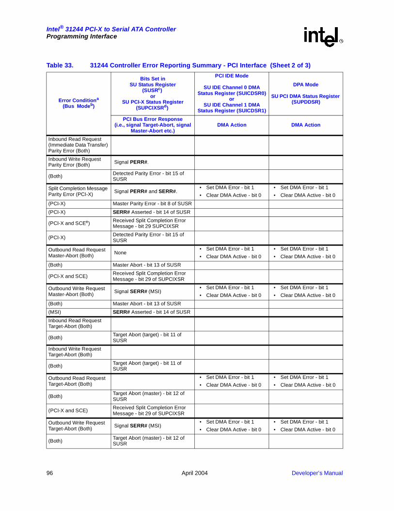
96 April 2004 Developer’s Manual
Intel® 31244 PCI-X to Serial ATA ControllerProgramming Interface
Inbound Read Request (Immediate Data Transfer) Parity Error (Both)
Inbound Write Request Parity Error (Both) Signal PERR#.
(Both) Detected Parity Error - bit 15 of SUSR
Split Completion Message Parity Error (PCI-X) Signal PERR# and SERR#.
• Set DMA Error - bit 1
• Clear DMA Active - bit 0
• Set DMA Error - bit 1
• Clear DMA Active - bit 0
(PCI-X) Master Parity Error - bit 8 of SUSR
(PCI-X) SERR# Asserted - bit 14 of SUSR
(PCI-X and SCEe) Received Split Completion Error Message - bit 29 SUPCIXSR
(PCI-X) Detected Parity Error - bit 15 of SUSR
Outbound Read Request Master-Abort (Both) None
• Set DMA Error - bit 1
• Clear DMA Active - bit 0
• Set DMA Error - bit 1
• Clear DMA Active - bit 0
(Both) Master Abort - bit 13 of SUSR
(PCI-X and SCE) Received Split Completion Error Message - bit 29 of SUPCIXSR
Outbound Write Request Master-Abort (Both) Signal SERR# (MSI)
• Set DMA Error - bit 1
• Clear DMA Active - bit 0
• Set DMA Error - bit 1
• Clear DMA Active - bit 0
(Both) Master Abort - bit 13 of SUSR
(MSI) SERR# Asserted - bit 14 of SUSR
Inbound Read Request Target-Abort (Both)
(Both) Target Abort (target) - bit 11 of SUSR
Inbound Write Request Target-Abort (Both)
(Both) Target Abort (target) - bit 11 of SUSR
Outbound Read Request Target-Abort (Both)
• Set DMA Error - bit 1
• Clear DMA Active - bit 0
• Set DMA Error - bit 1
• Clear DMA Active - bit 0
(Both) Target Abort (master) - bit 12 of SUSR
(PCI-X and SCE) Received Split Completion Error Message - bit 29 of SUPCIXSR
Outbound Write Request Target-Abort (Both) Signal SERR# (MSI)
• Set DMA Error - bit 1
• Clear DMA Active - bit 0
• Set DMA Error - bit 1
• Clear DMA Active - bit 0
(Both) Target Abort (master) - bit 12 of SUSR
Table 33. 31244 Controller Error Reporting Summary - PCI Interface (Sheet 2 of 3)
Error Conditiona
(Bus Modeb)
Bits Set inSU Status Register
(SUSRc)or
SU PCI-X Status Register(SUPCIXSRd)
PCI IDE Mode
SU IDE Channel 0 DMA Status Register (SUICDSR0)
orSU IDE Channel 1 DMA
Status Register (SUICDSR1)
DPA Mode
SU PCI DMA Status Register (SUPDDSR)
PCI Bus Error Response(i.e., signal Target-Abort, signal
Master-Abort etc.)DMA Action DMA Action
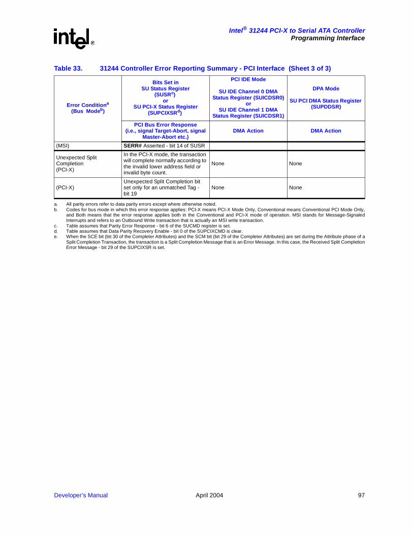
Developer’s Manual April 2004 97
Intel® 31244 PCI-X to Serial ATA ControllerProgramming Interface
(MSI) SERR# Asserted - bit 14 of SUSR
Unexpected Split Completion(PCI-X)
In the PCI-X mode, the transaction will complete normally according to the invalid lower address field or invalid byte count.
None None
(PCI-X)Unexpected Split Completion bit set only for an unmatched Tag - bit 19
None None
a. All parity errors refer to data parity errors except where otherwise noted.b. Codes for bus mode in which this error response applies: PCI-X means PCI-X Mode Only, Conventional means Conventional PCI Mode Only,
and Both means that the error response applies both in the Conventional and PCI-X mode of operation. MSI stands for Message-SignaledInterrupts and refers to an Outbound Write transaction that is actually an MSI write transaction.
c. Table assumes that Parity Error Response - bit 6 of the SUCMD register is set.d. Table assumes that Data Parity Recovery Enable - bit 0 of the SUPCIXCMD is clear.e. When the SCE bit (bit 30 of the Completer Attributes) and the SCM bit (bit 29 of the Completer Attributes) are set during the Attribute phase of a
Split Completion Transaction, the transaction is a Split Completion Message that is an Error Message. In this case, the Received Split CompletionError Message - bit 29 of the SUPCIXSR is set.
Table 33. 31244 Controller Error Reporting Summary - PCI Interface (Sheet 3 of 3)
Error Conditiona
(Bus Modeb)
Bits Set inSU Status Register
(SUSRc)or
SU PCI-X Status Register(SUPCIXSRd)
PCI IDE Mode
SU IDE Channel 0 DMA Status Register (SUICDSR0)
orSU IDE Channel 1 DMA
Status Register (SUICDSR1)
DPA Mode
SU PCI DMA Status Register (SUPDDSR)
PCI Bus Error Response(i.e., signal Target-Abort, signal
Master-Abort etc.)DMA Action DMA Action
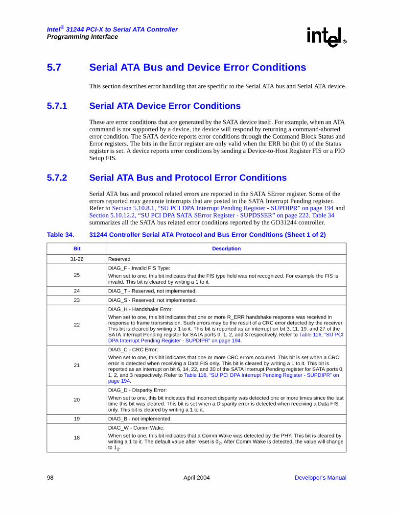
98 April 2004 Developer’s Manual
Intel® 31244 PCI-X to Serial ATA ControllerProgramming Interface
5.7 Serial ATA Bus and Device Error Conditions
This section describes error handling that are specific to the Serial ATA bus and Serial ATA device.
5.7.1 Serial ATA Device Error Conditions
These are error conditions that are generated by the SATA device itself. For example, when an ATA command is not supported by a device, the device will respond by returning a command-aborted error condition. The SATA device reports error conditions through the Command Block Status and Error registers. The bits in the Error register are only valid when the ERR bit (bit 0) of the Status register is set. A device reports error conditions by sending a Device-to-Host Register FIS or a PIO Setup FIS.
5.7.2 Serial ATA Bus and Protocol Error Conditions
Serial ATA bus and protocol related errors are reported in the SATA SError register. Some of the errors reported may generate interrupts that are posted in the SATA Interrupt Pending register. Refer to Section 5.10.8.1, “SU PCI DPA Interrupt Pending Register - SUPDIPR” on page 194 and Section 5.10.12.2, “SU PCI DPA SATA SError Register - SUPDSSER” on page 222. Table 34 summarizes all the SATA bus related error conditions reported by the GD31244 controller.
Table 34. 31244 Controller Serial ATA Protocol and Bus Error Conditions (Sheet 1 of 2)
Bit Description
31-26 Reserved
25DIAG_F - Invalid FIS Type:
When set to one, this bit indicates that the FIS type field was not recognized. For example the FIS is invalid. This bit is cleared by writing a 1 to it.
24 DIAG_T - Reserved, not implemented.
23 DIAG_S - Reserved, not implemented.
22
DIAG_H - Handshake Error:
When set to one, this bit indicates that one or more R_ERR handshake response was received in response to frame transmission. Such errors may be the result of a CRC error detected by the receiver. This bit is cleared by writing a 1 to it. This bit is reported as an interrupt on bit 3, 11, 19, and 27 of the SATA Interrupt Pending register for SATA ports 0, 1, 2, and 3 respectively. Refer to Table 116, “SU PCI DPA Interrupt Pending Register - SUPDIPR” on page 194.
21
DIAG_C - CRC Error:
When set to one, this bit indicates that one or more CRC errors occurred. This bit is set when a CRC error is detected when receiving a Data FIS only. This bit is cleared by writing a 1 to it. This bit is reported as an interrupt on bit 6, 14, 22, and 30 of the SATA Interrupt Pending register for SATA ports 0, 1, 2, and 3 respectively. Refer to Table 116, “SU PCI DPA Interrupt Pending Register - SUPDIPR” on page 194.
20
DIAG_D - Disparity Error:
When set to one, this bit indicates that incorrect disparity was detected one or more times since the last time this bit was cleared. This bit is set when a Disparity error is detected when receiving a Data FIS only. This bit is cleared by writing a 1 to it.
19 DIAG_B - not implemented.
18
DIAG_W - Comm Wake:
When set to one, this bit indicates that a Comm Wake was detected by the PHY. This bit is cleared by writing a 1 to it. The default value after reset is 02. After Comm Wake is detected, the value will change to 12.

Developer’s Manual April 2004 99
Intel® 31244 PCI-X to Serial ATA ControllerProgramming Interface
17 DIAG_I - Reserved, not implemented.
16
DIAG_N - PHYRDY Change State:
When set to one this bit indicates that the PHYRDY signal changed state. State change means going from ready-to-not ready or not ready-to-ready. This bit shall remain cleared when the PHY was not detected as ready during the initialization process. When the PHY goes ready after initialization, this bit shall transition to 1. This bit is cleared by writing a 1 to it. This bit is reported as an interrupt on bit 0, 8, 16, and 24 of the SATA Interrupt Pending register for SATA ports 0, 1, 2, and 3 respectively. Refer to Table 116, “SU PCI DPA Interrupt Pending Register - SUPDIPR” on page 194.
The default value after reset is 02, for example the PHY will not be ready. When the PHY becomes ready (state change from not ready to ready) as part of the initialization sequence, the value will change to 12.
15-12 Reserved.
11
ERR_E - Internal Error:
This bit indicates that a FIFO error occurred due to a FIFO overrun or underrun condition. This bit is cleared by writing a 1 to it. This bit is reported as an interrupt on bit 2, 10, 18, and 26 of the SATA Interrupt Pending register for SATA ports 0, 1, 2, and 3 respectively. Refer to Table 116, “SU PCI DPA Interrupt Pending Register - SUPDIPR” on page 194.
10
ERR_P - Protocol Error:
This bit when set indicates that a corrupted FIS was received. This bit may indicate that the FIS received was an invalid FIS type or that the received FIS was not properly structured. For example, incorrect length. This bit is cleared by writing a 1 to it. This bit is reported as an interrupt on bit 4, 12, 20, and 28 of the SATA Interrupt Pending register for SATA ports 0, 1, 2, and 3 respectively. Refer to Table 116, “SU PCI DPA Interrupt Pending Register - SUPDIPR” on page 194.
09
ERR_C - Non-Recovered Communication:
When set to one, this bit indicates that there is no signal detected on the PHY receive path (RX). This may occur from a faulty interconnect or the device has been removed. This bit is cleared by writing a 1 to it.
The default value after reset is 02. After reset, when a signal is not detected on the receive path (RX pair), the value will change to 12. After detecting a signal on the receive line, this bit will then change to 02.
08
ERR_T - Non-Recovered Transient Data Integrity Error:
This bit indicates that either a CRC error, disparity error, or the receipt of an R_ERR primitive occurred in response to a Data FIS. This bit is cleared by writing a 1 to it. This bit is reported as an interrupt on bit 5, 13, 21, and 29 of the SATA Interrupt Pending register for SATA ports 0, 1, 2, and 3 respectively. Refer to Table 116, “SU PCI DPA Interrupt Pending Register - SUPDIPR” on page 194.
07:02 Reserved
01
ERR_M - Recovered Communications Error:
This bit indicates that the PHY went from not ready-to-ready. This bit shall remain cleared when the PHY was not detected as ready during the initialization process. When the PHY goes ready after initialization, this bit shall transition to 1. This bit is cleared by writing a 1 to it. This bit is reported as an interrupt on bit 1, 9, 17, and 25 of the SATA Interrupt Pending register for SATA ports 0, 1, 2, and 3 respectively. Refer to Table 116, “SU PCI DPA Interrupt Pending Register - SUPDIPR” on page 194.
The default value after reset is 02, for example the PHY will not be ready. When the PHY becomes ready as part of the initialization sequence, the value will change to 12.
00 ERR_I - Reserved, not implemented.
Table 34. 31244 Controller Serial ATA Protocol and Bus Error Conditions (Sheet 2 of 2)
Bit Description
100 April 2004 Developer’s Manual
Intel® 31244 PCI-X to Serial ATA ControllerProgramming Interface
5.8 SATA Port Interrupt Generation
When the SATA Unit on the GD31244 controller is in PCI IDE mode, interrupts that are generated follow the ATA standard. An ATA device generates an interrupt using the INTRQ hardware signal during normal data transfer to indicate data transfer completion and/or to indicate an error condition. An error condition is indicated when the ERR bit (bit 0) in the Status register is set. In contrast, a SATA device indicates an interrupt by using the ‘I’ bit (a pseudo INTRQ signal) in the PIO Setup FIS, or the Device-to-Host Register FIS. A hardware interrupt is then generated based on the ‘I’ being set.
When the SATA Unit operates in PCI DPA Mode, interrupts may also be generated by bits being set in the SATA SError Registers, in addition to the normal ATA standard interrupts explained above. Refer to Table 136, “SU PCI DPA SATA SError Register - SUPDSSER” on page 222, and Table 116, “SU PCI DPA Interrupt Pending Register - SUPDIPR” on page 194.
The block diagram in Figure 31 shows how each SATA Unit generates and posts interrupts coming from the SATA ports. SATA Unit posted interrupts are routed onto PCI interrupt line - PINTA#.
Interrupts may also be generated using Message-Signaled Interrupts. Refer to Section 5.9, “Message-Signaled Interrupts” on page 102. When MSI is enabled, the GD31244 controller will not generate interrupts using the interrupt line - PINTA#.

Developer’s Manual April 2004 101
Intel® 31244 PCI-X to Serial ATA ControllerProgramming Interface
Figure 31. SATA Unit Interrupt Generation Block Diagram
SATA Device
SATA
OROR
Direct Port Access ModePCI IDE Mode
Interrupts
SError
Port 3Interrupts
To PCI Interrupt Pin - PINTA#
Port 0
Port 3
SATA
Mask Bits provided
Device ControlRegister (nIEN)
NOTES:Port 0 SError bits are reported on bits 6-0Port 1 SError bits are reported on bits 14-8Port 2 SError bits are reported on bits 22-16Port 3 SError bits are reported on bits 30-24
Interrupt
Interrupt
Mask
Pending
Register
Register
Port 1Port 2
031 15 14 30 23 22
Port 0- Port 3
24 16 7 6 8
SError
Port 2Interrupts
SError
Port 1Interrupts
SError
Port 0Interrupts
031 15 14 30 23 22 24 16 7 6 8
102 April 2004 Developer’s Manual
Intel® 31244 PCI-X to Serial ATA ControllerProgramming Interface
5.9 Message-Signaled Interrupts
The GD31244 controller may deliver interrupt to the Host Processor through the P_INTA# output pin or the Message Signaled Interrupt (MSI) mechanism.
When a host processor enables Message-Signaled Interrupts (MSI) on the GD31244 controller, a SATA Unit interrupt will be signaled to the host through a PCI write instead of the assertion of the P_INTA# output pin.
PCI-X Addendum to the PCI Local Bus Specification, Revision 1.0a states: “PCI-X devices that generate interrupts are required to support message-signaled interrupts, as defined by the PCI Local Bus Specification, Revision 2.2 and must support a 64-bit message address.” “Devices that require interrupts in systems that do not support message-signaled interrupts, must implement interrupt pins.” Thus, the GD31244 controller needs to implement both wired and message-signaled interrupt delivery mechanisms.
In support of MSI, the GD31244 controller will implement the MSI capability structure. The capability structure includes the “SU MSI Message Control Register - SUMSI_Message_Control” on page 162, the “SU MSI Message Address Register - SUMSI_Message_Address” on page 163, the “SU MSI Message Upper Address Register - SUMSI_Message_Upper_Address” on page 164 and the“SU MSI Message Data Register - SUMSI_Message_Data” on page 165.
During system initialization, the configuration software for an MSI system will read the Message Control Register to determine that the GD31244 controller supports a 64-bit Message Address, and that it is capable of generating four unique interrupt messages.
After gathering this data from all of the MSI capable devices in the system, the configuration software will decide where to initialize the Message Address and how many unique messages each MSI capable device is allowed. Then, software will write the Message Address Registers (and the Message Upper Address Registers when Message Address is above the 4G address boundary1), and the Message Data Register. This system specified data will be used to route the interrupt request message to the appropriate entry in a host processor Local APIC table.
Configuration of MSI completes with a write to the Message Control Register which includes an update to the Multiple Message Enable field and the MSI enable bit of each device. This will inform the device how many unique messages (Local APIC table entries) have been allocated for exclusive use by that device and enable that device for MSI. Device hardware is required to handle allocation of fewer unique interrupt messages than requested by the Multiple Message Capable field.
The GD31244 controller may generate up to four messages - one per SATA port, but it is also able to generate less than four messages - two or one message. Interrupt handler software needs to read the SATA port status and interrupt pending registers to determine the cause of the interrupt when more than one SATA ports are represented by less than four MSI messages.
Note: When host software enables MSI, the interrupt will not result in the assertion of the P_INTA# output pin.
5.9.1 Level-Triggered Versus Edge-Triggered Interrupts
When MSI is disabled, the P_INTA# pin remains asserted and pended to the host when any of the SATA Unit interrupt sources requires service. Since the PCI pin signaled interrupt is level-triggered, the interrupt service routine will not drop out of the service routine until the interrupt signal is deasserted. This will ensure that an interrupt will not be missed.
MSI interrupts are inherently edge-triggered, in that an interrupt is only pended to the host as a write event when any of the SATA Port requires service.
1. When host software writes the Message Upper address register to a non-zero value, device hardware will use a write transaction with a Dual Address Cycle (DAC) to present the full 64-bit address to the bus.

Developer’s Manual April 2004 103
Intel® 31244 PCI-X to Serial ATA ControllerProgramming Interface
5.10 Register Definitions
The section is broken into three subsections. Each subsection describes a different programming interface.
• PCI IDE Mode Registers
• Direct Port Access Mode Registers
5.10.1 PCI IDE Mode Registers
This section defines the SATA port registers as viewed from the PCI bus when in PCI IDE mode
Every PCI device/function implements its own separate configuration address space and configuration registers. The PCI Local Bus Specification, Revision 2.2 requires that configuration space be 256 bytes, and the first 64 bytes must adhere to a predefined header format.
Figure 32 defines the header format. Table 35 shows the PCI configuration registers. Table 35 shows the entire Serial ATA Unit configuration space (including header and extended registers) and the corresponding section that describes each register.
The Serial ATA Unit is programmed through a Type 0 configuration command on the PCI interface. Serial ATA Unit (SU) configuration space is function number zero.
Beyond the required 64-byte header format, Serial ATA Unit configuration space implements extended register space in support of the unit functionality. Refer to the PCI Local Bus Specification, Revision 2.2 for details on accessing and programming configuration register space.
Figure 32. SU in PCI IDE Mode Interface Configuration Header Format
Device ID Vendor ID 00H
Status Command 04H
Class Code Revision ID 08H
BIST Header Type Latency Timer Cacheline Size 0CH
Base Address 0 10H
Base Address 1 14H
Base Address 2 18H
Base Address 3 1CH
Base Address 4 20H
Base Address 5 24H
Reserved 28H
Subsystem ID Subsystem Vendor ID 2CH
Expansion ROM Base Address 30H
Reserved Capabilities Pointer 34H
Reserved 38H
Maximum Latency Minimum Grant Interrupt Pin Interrupt Line 3CH

104 April 2004 Developer’s Manual
Intel® 31244 PCI-X to Serial ATA ControllerProgramming Interface
The Serial ATA Unit includes two 8 byte and one 16-byte extended capability configuration spaces beginning at configuration offset E0H, E8H and F0H. The extended configuration spaces may be accessed by a device on the PCI interface through a mechanism defined in the PCI Local Bus Specification, Revision 2.2.
In the SU Status Register (Section 5.10.2.4) the appropriate bit is set indicating that the Extended Capability Configuration space is supported. When this bit is read, the device may then read the Capabilities Pointer register (Section 5.10.2.20) to determine the configuration offset of the Extended Capabilities Configuration Header. The format of these headers are depicted in Figure 33 through Figure 35.
The first byte at the Extended Configuration Offset E0H is the PCI-X Capability Identifier Register (Section 5.10.2.42). This will identify this Extended Configuration Header space as the type defined by the PCI-X Addendum to the PCI Local Bus Specification, Revision 1.0a.
Following the Capability Identifier Register will be the single byte Next Item Pointer Register (Section 5.10.2.43) which will indicate the configuration offset of an additional Extended Capabilities Header, when supported. In the SATA Unit, the Next Item Pointer Register is set to E8H indicating that there are additional Extended Capabilities Headers supported in the SATA Unit configuration space.
.
The first byte at the Extended Configuration Offset E8H is the SATA Unit Capability Identifier Register (Section 5.10.2.46). This will identify this Extended Configuration Header space as the type defined by the PCI Bus Power Management Interface Specification, Revision 1.1.
Following the Capability Identifier Register will be the single byte Next Item Pointer Register (Section 5.10.2.47) which will indicate the configuration offset of an additional Extended Capabilities Header, when supported. In the Serial ATA Unit, the Next Item Pointer Register is set to F0H indicating that there are additional Extended Capabilities Headers supported in the Serial ATA Unit configuration space.
It is the configuration software responsibility to properly enable and initialize the SATA Unit Power Management Interface.
Figure 33. SATA Unit Interface Extended Configuration Header Format (PCI-X Capability)
E0H
E4H
PCI-X Capability IDNext Item PointerPCI-X Command
PCI-X Status
Figure 34. SU in PCI IDE Mode Interface Extended Configuration Header Format (Power Management)
E8H
ECH
Capability IdentifierNext Item PointerPower Management Capabilities
Power Management Control/StatusReserved

Developer’s Manual April 2004 105
Intel® 31244 PCI-X to Serial ATA ControllerProgramming Interface
The first byte at the Extended Configuration Offset F0H is the MSI Capability Identifier Register (Section 5.10.2.50). This will identify this Extended Configuration Header space as the type defined by the PCI Local Bus Specification, Revision 2.2.
Following the Capability Identifier Register will be the single byte Next Item Pointer Register (Section 5.10.2.51) which will indicate the configuration offset of an additional Extended Capabilities Header, when supported. In the SATA Unit, the Next Item Pointer Register is set to 00H indicating that there is no additional Extended Capabilities Headers supported in the SATA Unit configuration space.
The following sections describe the Serial ATA Unit configuration registers. Configuration space consists of 8-, 16-, 24-, and 32-bit registers arranged in a predefined format. Each register is described in functionality, access type (read/write, read/clear, read only) and reset default condition.
See Section 1.2, “Terminology and Conventions” on page 16 for a description of reserved, read only, and read/clear. All registers adhere to the definitions found in the PCI Local Bus Specification, Revision 2.2 unless otherwise noted.
The PCI register number for each register is given in Table 35. As stated, a Type 0 configuration command on the bus with an active IDSEL.
Figure 35. SU in PCI IDE Mode Interface Extended Configuration Header Format (MSI Capability)
F0H
F4H
MSI Capability IDMSI Next Item PointerMSI Message Control
MSI Message Address
MSI Message Upper Address F8H
FCHMSI Message DataReserved
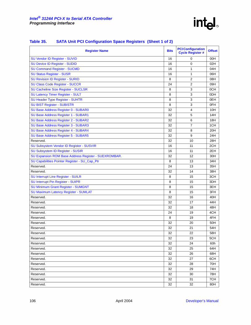
106 April 2004 Developer’s Manual
Intel® 31244 PCI-X to Serial ATA ControllerProgramming Interface
Table 35. SATA Unit PCI Configuration Space Registers (Sheet 1 of 2)
Register Name Bits PCI Configuration Cycle Register # Offset
SU Vendor ID Register - SUVID 16 0 00H
SU Device ID Register - SUDID 16 0 02H
SU Command Register - SUCMD 16 1 04H
SU Status Register - SUSR 16 1 06H
SU Revision ID Register - SURID 8 2 08H
SU Class Code Register - SUCCR 24 2 09H
SU Cacheline Size Register - SUCLSR 8 3 0CH
SU Latency Timer Register - SULT 8 3 0DH
SU Header Type Register - SUHTR 8 3 0EH
SU BIST Register - SUBISTR 8 3 0FH
SU Base Address Register 0 - SUBAR0 32 4 10H
SU Base Address Register 1 - SUBAR1 32 5 14H
SU Base Address Register 2 - SUBAR2 32 6 18H
SU Base Address Register 3 - SUBAR3 32 7 1CH
SU Base Address Register 4 - SUBAR4 32 8 20H
SU Base Address Register 5 - SUBAR5 32 9 24H
Reserved. 32 10 28H
SU Subsystem Vendor ID Register - SUSVIR 16 11 2CH
SU Subsystem ID Register - SUSIR 16 11 2EH
SU Expansion ROM Base Address Register - SUEXROMBAR. 32 12 30H
SU Capabilities Pointer Register - SU_Cap_Ptr 8 13 34H
Reserved. 24 13 35H
Reserved. 32 14 38H
SU Interrupt Line Register - SUILR 8 15 3CH
SU Interrupt Pin Register - SUIPR 8 15 3DH
SU Minimum Grant Register - SUMGNT 8 15 3EH
SU Maximum Latency Register - SUMLAT 8 15 3FH
Reserved. 32 16 40H
Reserved. 32 17 44H
Reserved. 32 18 48H
Reserved. 24 19 4CH
Reserved. 8 19 4FH
Reserved. 32 20 50H
Reserved. 32 21 54H
Reserved. 32 22 58H
Reserved. 32 23 5CH
Reserved. 32 24 60h
Reserved. 32 25 64H
Reserved. 32 26 68H
Reserved. 32 27 6CH
Reserved. 32 28 70H
Reserved. 32 29 74H
Reserved. 32 30 78H
Reserved. 32 31 7CH
Reserved. 32 32 80H

Developer’s Manual April 2004 107
Intel® 31244 PCI-X to Serial ATA ControllerProgramming Interface
s
Reserved. 32 33 84H
Reserved. 32 34 88H
Reserved. 32 35 8CH
SPI Command Register - SPICMDR 8 36 90H
SPI Control Register - SPICNTR 8 36 91H
SPI Status Register - SPISTATR 8 36 92H
Reserved. 8 36 93H
SPI Data Register - SPIDATR 32 37 94H
Reserved. 16 37 96H
SU Extended Control and Status Register 0 - SUECSR 0 32 38 98H
Reserved. 32 39 9CH
SU DMA Control Status Register- SUDCSCR 32 40 A0H
SU Dummy Register SUDR 32 41 A4H
SU Interrupt Status Register SUISR 32 42 A8H
SU Interrupt Mask Register SUIMR 32 43 ACH
Reserved. 32 44 B0H
Reserved. 32 45 B4H
Reserved. 32 46 B8H
Reserved. 32 47 BCH
SU Transaction Control SUTCR 32 48 C0H
SU Target Split Completion Message Enable Register SUTSCMER 32 49 C4H
SU Target Delayed/Split Request Pending Register SUDRPR 32 50 C8H
SU Transaction Control 2 Register SUTC2R 32 51 CCH
SU Master Deferred/Split Sequence Pending Register - SUMDSPR 32 52 D0H
SU Master Split Completion Message Received with Error Message Register - SUMSCMREMR 32 53 D4H
SU Arbiter Control - SUACR 32 54 D8H
Reserved. 32 55 DCH
SU PCI-X_Capability Identifier Register - SUPCI-X_Cap_ID 8 56 E0H
SU PCI-X Next Item Pointer Register - SUPCI-X_Next_Item_Ptr 8 56 E1H
SU PCI-X Command Register - SUPCIXCMD 16 56 E2H
SU PCI-X Status Register - SUPCIXSR 32 57 E4H
SU PM_Capability Identifier Register - SUPM_Cap_ID 8 58 E8H
SU PM Next Item Pointer Register - SUPM_Next_Item_Ptr 8 58 E9H
SU Power Management Capabilities Register - SUPMCR 16 58 EAH
SU Power Management Control/Status Register - SUPMCSR 16 59 ECH
Reserved. 16 59 EEH
SU MSI Capability Identifier Register - SUMSI_Cap_ID 8 60 F0H
SU MSI Next Item Pointer Register - SUMSI_Next_Ptr 8 60 F1H
SU MSI Message Control Register - SUMSI_Message_Control 16 60 F2H
SU MSI Message Address Register - SUMSI_Message_Address 32 61 F4H
SU MSI Message Upper Address Register - SUMSI_Message_Upper_Address 32 62 F8H
SU MSI Message Data Register - SUMSI_Message_Data 16 63 FCH
Table 35. SATA Unit PCI Configuration Space Registers (Sheet 2 of 2)
Register Name Bits PCI Configuration Cycle Register # Offset

108 April 2004 Developer’s Manual
Intel® 31244 PCI-X to Serial ATA ControllerProgramming Interface
s
Table 36. SATA Command Block Registers in PCI IDE Mode
Register Name Bits Access BAR 0/2 + Offset
SU IDE Data Port Register - SUIDR 16 Read/Write 00H
SU IDE Error Register - SUIER 8 Read Only 01H
SU IDE Features Register - SUIFR 8 Write Only 01H
SU IDE Sector Count Register - SUISCR 8 Read/Write 02H
SU IDE Sector Number Register - SUISNR 8 Read/Write 03H
SU IDE Cylinder Low Register - SUICLR 8 Read/Write 04H
SU IDE Cylinder High Register - SUICHR 8 Read/Write 05H
SU IDE Device/Head Register - SUIDHR 8 Read/Write 06H
SU IDE Status Register - SUISR 8 Write Only 07H
SU IDE Command Register - SUICR 8 Read Only 07H
NOTE: In Native-PCI mode, the offset is relative to the PCI Base Address Registers at offset 10H and 18H in the PCI Configuration Space. Base Address Register at offset 10H points to Channel 0. And Base Address Register at offset 18H points to Channel 1.
Table 37. SATA Control Block Registers in PCI IDE Mode
Register Name Bits Access BAR 0/2 + Offset
Reserved. 8 00H
Reserved. 8 01H
SU IDE Device Control Register - SUIDCR 8 Write Only 02H
SU IDE Alternate Status Register - SUIASR 8 Read Only 02H
Reserved. 8 03H
NOTE: In Native-PCI mode, the offset is relative to the PCI Base Address Registers at offset 14H and 1CH in the PCI Configuration Space. Base Address Register at offset 14H points to Channel 0. And Base Address Register at offset 1CH points to Channel 1.
Table 38. SATA DMA Registers in PCI IDE Mode
Register Name Bits Offset
SU IDE Channel 0 DMA Command Register - SUICDCR0 8 00H
Reserved 8 01H
SU IDE Channel 0 DMA Status Register - SUICDSR0 8 02H
Reserved 8 03H
SU IDE Channel 0 DMA Descriptor Table Pointer Register - SUICDDTPR0 32 04H
SU IDE Channel 1 DMA Command Register - SUICDCR1 8 08H
Reserved 8 09H
SU IDE Channel 1 DMA Status Register - SUICDSR1 8 0AH
Reserved 8 0BH
SU IDE Channel 1 DMA Descriptor Table Pointer Register - SUICDDTPR1 32 0CH
NOTE: The offset is relative to the PCI Base Address Register at offset 20H in the PCI Configuration Space.

Developer’s Manual April 2004 109
Intel® 31244 PCI-X to Serial ATA ControllerProgramming Interface
5.10.2 PCI Configuration Registers
This section defines the PCI configuration registers.
5.10.2.1 SU Vendor ID Register - SUVID
SU Vendor ID Register bits adhere to the definitions in the PCI Local Bus Specification, Revision 2.2.
Table 39. SU Vendor ID Register - SUVID
Bit Default Description
15:00 8086H
SU Vendor ID - This is a 16-bit value assigned to Intel. This register, combined with the DID, uniquely identify the PCI device. Access type is Read/Write to allow the GD31244 controller to configure the register as a different vendor ID to simulate the interface of a standard mechanism currently used by existing application software.
PCIAttributes
15 12 8 4 0
ro ro ro ro ro ro ro ro ro ro ro ro ro ro ro ro
Attribute Legend:RV = ReservedPR = PreservedRS = Read/Set
RW = Read/WriteRC = Read ClearRO = Read OnlyNA = Not Accessible
PCI Configuration Address Offset
00H - 01H

110 April 2004 Developer’s Manual
Intel® 31244 PCI-X to Serial ATA ControllerProgramming Interface
5.10.2.2 SU Device ID Register - SUDID
SU Device ID Register bits adhere to the definitions in the PCI Local Bus Specification, Revision 2.2.
Table 40. SU Device ID Register - SUDID
Bit Default Description
15:00 3200H SU Device ID - This is a 16-bit value assigned to the SATA Unit. This ID, combined with the VID, uniquely identify any PCI device.
PCIAttributes
15 12 8 4 0
ro ro ro ro ro ro ro ro ro ro ro ro ro ro ro ro
Attribute Legend:RV = ReservedPR = PreservedRS = Read/Set
RW = Read/WriteRC = Read ClearRO = Read OnlyNA = Not Accessible
PCI Configuration Address Offset
02H - 03H
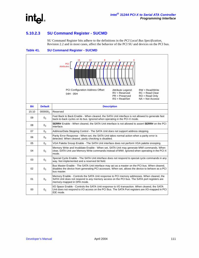
Developer’s Manual April 2004 111
Intel® 31244 PCI-X to Serial ATA ControllerProgramming Interface
5.10.2.3 SU Command Register - SUCMD
SU Command Register bits adhere to the definitions in the PCI Local Bus Specification, Revision 2.2 and in most cases, affect the behavior of the PCI SU and devices on the PCI bus.
Table 41. SU Command Register - SUCMD
Bit Default Description
15:10 0000002 Reserved
09 02Fast Back to Back Enable - When cleared, the SATA Unit interface is not allowed to generate fast back-to-back cycles on its bus. Ignored when operating in the PCI-X mode.
08 02SERR# Enable - When cleared, the SATA Unit interface is not allowed to assert SERR# on the PCI interface.
07 02 Address/Data Stepping Control - The SATA Unit does not support address stepping.
06 02Parity Error Response - When set, the SATA Unit takes normal action when a parity error is detected. When cleared, parity checking is disabled.
05 02 VGA Palette Snoop Enable - The SATA Unit interface does not perform VGA palette snooping.
04 02
Memory Write and Invalidate Enable - When set, SATA Unit may generate MWI commands. When clear, SATA Unit use Memory Write commands instead of MWI. Ignored when operating in the PCI-X mode.
03 02Special Cycle Enable - The SATA Unit interface does not respond to special cycle commands in any way. Not implemented and a reserved bit field.
02 02
Bus Master Enable - The SATA Unit interface may act as a master on the PCI bus. When cleared, disables the device from generating PCI accesses. When set, allows the device to behave as a PCI bus master.
01 02
Memory Enable - Controls the SATA Unit response to PCI memory addresses. When cleared, the SATA Unit does not respond to any memory access on the PCI bus. The SATA port registers are memory-mapped in DPA mode.
00 02
I/O Space Enable - Controls the SATA Unit response to I/O transaction. When cleared, the SATA Unit does not respond to I/O access on the PCI Bus. The SATA Port registers are I/O-mapped in PCI IDE mode.
PCIAttributes
15 12 8 4 0
rv rv rv rv rv rv rw rw ro rw ro rw ro rw rw rw
Attribute Legend:RV = ReservedPR = PreservedRS = Read/Set
RW = Read/WriteRC = Read ClearRO = Read OnlyNA = Not Accessib
PCI Configuration Address Offset
04H - 05H
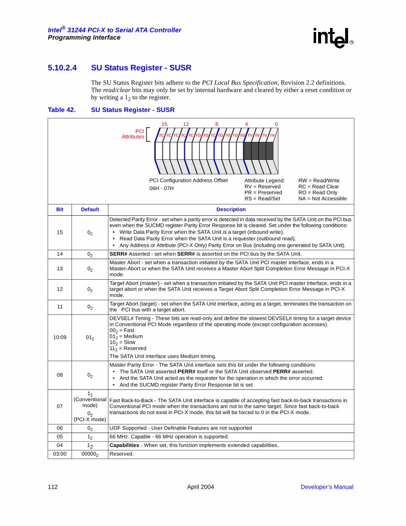
112 April 2004 Developer’s Manual
Intel® 31244 PCI-X to Serial ATA ControllerProgramming Interface
5.10.2.4 SU Status Register - SUSR
The SU Status Register bits adhere to the PCI Local Bus Specification, Revision 2.2 definitions. The read/clear bits may only be set by internal hardware and cleared by either a reset condition or by writing a 12 to the register.
Table 42. SU Status Register - SUSR
Bit Default Description
15 02
Detected Parity Error - set when a parity error is detected in data received by the SATA Unit on the PCI bus even when the SUCMD register Parity Error Response bit is cleared. Set under the following conditions:
• Write Data Parity Error when the SATA Unit is a target (inbound write).• Read Data Parity Error when the SATA Unit is a requester (outbound read).• Any Address or Attribute (PCI-X Only) Parity Error on Bus (including one generated by SATA Unit).
14 02 SERR# Asserted - set when SERR# is asserted on the PCI bus by the SATA Unit.
13 02
Master Abort - set when a transaction initiated by the SATA Unit PCI master interface, ends in a Master-Abort or when the SATA Unit receives a Master Abort Split Completion Error Message in PCI-X mode.
12 02
Target Abort (master) - set when a transaction initiated by the SATA Unit PCI master interface, ends in a target abort or when the SATA Unit receives a Target Abort Split Completion Error Message in PCI-X mode.
11 02Target Abort (target) - set when the SATA Unit interface, acting as a target, terminates the transaction on the PCI bus with a target abort.
10:09 012
DEVSEL# Timing - These bits are read-only and define the slowest DEVSEL# timing for a target device in Conventional PCI Mode regardless of the operating mode (except configuration accesses).002 = Fast012 = Medium102 = Slow112 = Reserved
The SATA Unit interface uses Medium timing.
08 02
Master Parity Error - The SATA Unit interface sets this bit under the following conditions:• The SATA Unit asserted PERR# itself or the SATA Unit observed PERR# asserted.• And the SATA Unit acted as the requester for the operation in which the error occurred.• And the SUCMD register Parity Error Response bit is set
07
12 (Conventional
mode)
02 (PCI-X mode)
Fast Back-to-Back - The SATA Unit interface is capable of accepting fast back-to-back transactions in Conventional PCI mode when the transactions are not to the same target. Since fast back-to-back transactions do not exist in PCI-X mode, this bit will be forced to 0 in the PCI-X mode.
06 02 UDF Supported - User Definable Features are not supported
05 12 66 MHz. Capable - 66 MHz operation is supported.
04 12 Capabilities - When set, this function implements extended capabilities.
03:00 000002 Reserved.
PCIAttributes
15 12 8 4 0
rc rc rc rc rc ro ro rc ro ro ro ro rv rv rv rv
Attribute Legend:RV = ReservedPR = PreservedRS = Read/Set
RW = Read/WriteRC = Read ClearRO = Read OnlyNA = Not Accessible
PCI Configuration Address Offset
06H - 07H

Developer’s Manual April 2004 113
Intel® 31244 PCI-X to Serial ATA ControllerProgramming Interface
5.10.2.5 SU Revision ID Register - SURID
Revision ID Register bit definitions adhere to PCI Local Bus Specification, Revision 2.2.
Table 43. SU Revision ID Register - SURID
Bit Default Description
07:00 00H SU Revision - identifies the GD31244 controller revision number.
PCIAttributes
7 4 0
ro ro ro ro ro ro ro ro
Attribute Legend:RV = ReservedPR = PreservedRS = Read/Set
RW = Read/WriteRC = Read ClearRO = Read OnlyNA = Not Accessible
PCI Configuration Address Offset
08H

114 April 2004 Developer’s Manual
Intel® 31244 PCI-X to Serial ATA ControllerProgramming Interface
5.10.2.6 SU Class Code Register - SUCCR
Class Code Register bit definitions adhere to PCI Local Bus Specification, Revision 2.2. Auto configuration software reads this register to determine the PCI device function.
Table 44. SU Class Code Register - SUCCR
Bit Default Description
23:16 01H Base Class - Mass Storage Device
15:08Varies with
external state of DPA_MODE# pin
Sub Class -
• When in Direct Port Access Mode (DPA_MODE# = low)
= 06H - DPA Mode
• When in PCI IDE Mode (DPA_MODE# = high)
= 01H - PCI IDE
07:04Varies with
external state of DPA_MODE# pin
Programming Interface -
• When in Direct Port Access Mode (DPA_MODE# = low)
= 00002
• When in PCI IDE Mode (DPA_MODE# = high)
= 10002 - Bit 7 set identifies the PCI IDE device as a Bus Master
03:00Varies with
external state of DPA_MODE# pin
Programming Interface -
• When in Direct Port Access Mode (DPA_MODE# = low)
= 00002
• When in PCI IDE Mode (DPA_MODE# = high)
= 01012 - SATA Unit supports Native-PCI mode only
PCIAttributes
23 20 16 12 8 4 0
ro ro ro ro ro ro ro ro ro ro ro ro ro ro ro ro ro ro ro ro ro ro ro ro
Attribute Legend:RV = ReservedPR = PreservedRS = Read/Set
RW = Read/WriteRC = Read ClearRO = Read OnlyNA = Not Accessible
PCI Configuration Address Offset
09H - 0BH

Developer’s Manual April 2004 115
Intel® 31244 PCI-X to Serial ATA ControllerProgramming Interface
5.10.2.7 SU Cacheline Size Register - SUCLSR
Cacheline Size Register bit definitions adhere to PCI Local Bus Specification, Revision 2.2. This register is programmed with the system cacheline size in DWORDs (32-bit words). The GD31244 controller may burst up to a maximum of 512 bytes per request. The Cacheline Size register defines burst boundaries for bus master/DMA transactions generated by the GD31244 controller. For example, when a DMA transaction starts on a non-aligned cacheline address, the DMA controller starts the transaction by bursting from that unaligned address until the next cacheline boundary is reached. Subsequent DMA transactions then starts on cacheline boundaries and burst up to a maximum of 512 bytes. A value of zero means that burst transactions takes place on unaligned boundaries, transferring up to 512 bytes.
Table 45. SU Cacheline Size Register - SUCLSR
Bit Default Description
07:00 00H
SU Cacheline Size - CLS specifies the system cacheline size in DWORDs.
CLS Burst Length
00 80h, 40h, 20h, 10h, 08h
08 80h, 40h, 20h, 10h, 08h
10 80h, 40h, 20h,10h
20 80h, 40h, 20h
40 80h, 40h
80 80h
other 80h, 40h, 20h, 10h, 08h
PCIAttributes
7 4 0
rw rw rw rw rw rw rw rw
Attribute Legend:RV = ReservedPR = PreservedRS = Read/Set
RW = Read/WriteRC = Read ClearRO = Read OnlyNA = Not Accessible
PCI Configuration Address Offset
0CH

116 April 2004 Developer’s Manual
Intel® 31244 PCI-X to Serial ATA ControllerProgramming Interface
5.10.2.8 SU Latency Timer Register - SULT
SU Latency Timer Register bit definitions apply to the PCI interface.
Table 46. SU Latency Timer Register - SULT
Bit Default Description
07:00
00H(Conventional
Mode)
40H(PCI-X Mode)
Programmable Latency Timer - This field varies the latency timer for the interface from 0 to 248 clocks. The default value is 0 clocks for Conventional PCI mode, and 64 clocks for PCI-X mode.
PCIAttributes
7 4 0
rw rw rw rw rw rw rw rw
Attribute Legend:RV = ReservedPR = PreservedRS = Read/Set
RW = Read/WriteRC = Read ClearRO = Read OnlyNA = Not Accessible
PCI Configuration Address Offset
0DH

Developer’s Manual April 2004 117
Intel® 31244 PCI-X to Serial ATA ControllerProgramming Interface
5.10.2.9 SU Header Type Register - SUHTR
Header Type Register bit definitions adhere to PCI Local Bus Specification, Revision 2.2. This register indicates the layout of SATA Unit configuration space bytes 10H to 3FH. The MSB indicates whether or not the device is multi-function.
Table 47. SU Header Type Register - SUHTR
Bit Default Description
07 02Single Function/Multi-Function Device - Identifies the GD31244 controller as a single-function PCI device.
06:00 0000002PCI Header Type - This bit field indicates the type of PCI header implemented. The SATA Unit interface header conforms to PCI Local Bus Specification, Revision 2.2.
PCIAttributes
7 4 0
ro ro ro ro ro ro ro ro
Attribute Legend:RV = ReservedPR = PreservedRS = Read/Set
RW = Read/WriteRC = Read ClearRO = Read OnlyNA = Not Accessible
PCI Configuration Address Offset
0EH

118 April 2004 Developer’s Manual
Intel® 31244 PCI-X to Serial ATA ControllerProgramming Interface
5.10.2.10 SU BIST Register - SUBISTR
The SU BIST Register bit definitions adhere to PCI Local Bus Specification, Revision 2.2.
Table 48. SU BIST Register - SUBISTR
Bit Default Description
07 02 BIST Capable - This bit always returns a zero, meaning that this unit is not BIST capable.
06 02 Start BIST - Writing a one to this bit will invoke BIST. This bit will stay high until BIST is complete.
05:04 002 Reserved
03:00 00002 BIST Completion Code.
PCIAttributes
7 4 0
ro rw rv rv rw rw rw rw
PCI Configuration Address Offset
0FH
Attribute Legend:RV = ReservedPR = PreservedRS = Read/Set
RW = Read/WriteRC = Read ClearRO = Read OnlyNA = Not Accessible

Developer’s Manual April 2004 119
Intel® 31244 PCI-X to Serial ATA ControllerProgramming Interface
5.10.2.11 SU Base Address Register 0 - SUBAR0
The SU Base Address Register 0 (SUBAR0) defines the base I/O address of the Command Block Registers for Channel 0.
Table 49. SU Base Address Register 0 - SUBAR0
Bit Default PCI IDE Description
31:00 0000_01F1H Base Address 0 - These bits define the base address of the Command Block Registers in PCI I/O space for channel 0.
DPA Mode Description
31:00 0000_0004H Base Address 0 - 4K of memory for all port registers. Lower 32 bit address.
PCIAttributes
28 24 20 16 12 8 4 031
rw rw rw rw rw rw rw rw rw rw rw rw rw rw rw rw rw rw rw rw rw rw rw rw rw rw rw rw rw rv rv ro
Attribute Legend:RV = ReservedPR = PreservedRS = Read/Set
RW = Read/WriteRC = Read ClearRO = Read OnlyNA = Not Accessible
PCI Configuration Address Offset
10H - 13H

120 April 2004 Developer’s Manual
Intel® 31244 PCI-X to Serial ATA ControllerProgramming Interface
5.10.2.12 SU Base Address Register 1 - SUBAR1
The SU Base Address Register 1 (SUBAR1) defines the base I/O address of the Control Block Registers for Channel 0.
Table 50. SU Base Address Register 1 - SUBAR1
Bit Default PCI IDE Description
31:00 0000_03F5H Base Address 1 - PCI IDE Mode: These bits define the base address of the Control Block Registers in PCI I/O space for channel 0.
DPA Mode
31:00 0000_0000H Base Address 1 - DPA Mode Upper 32 bits for BAR0
PCIAttributes
28 24 20 16 12 8 4 031
rw rw rw rw rw rw rw rw rw rw rw rw rw rw rw rw rw rw rw rw rw rw rw rw rw rw rw rw rw rw rv ro
Attribute Legend:RV = ReservedPR = PreservedRS = Read/Set
RW = Read/WriteRC = Read ClearRO = Read OnlyNA = Not Accessible
PCI Configuration Address Offset
14H - 17H
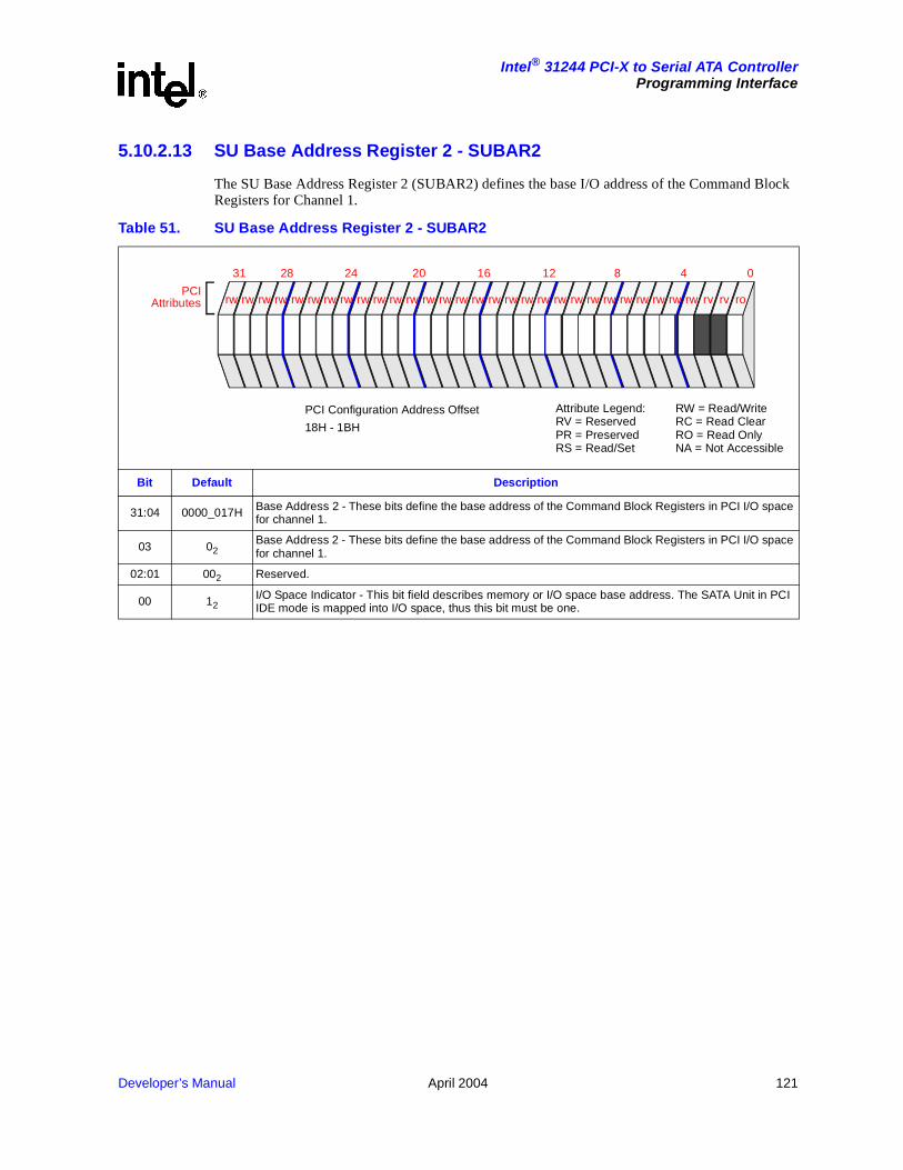
Developer’s Manual April 2004 121
Intel® 31244 PCI-X to Serial ATA ControllerProgramming Interface
5.10.2.13 SU Base Address Register 2 - SUBAR2
The SU Base Address Register 2 (SUBAR2) defines the base I/O address of the Command Block Registers for Channel 1.
Table 51. SU Base Address Register 2 - SUBAR2
Bit Default Description
31:04 0000_017H Base Address 2 - These bits define the base address of the Command Block Registers in PCI I/O space for channel 1.
03 02Base Address 2 - These bits define the base address of the Command Block Registers in PCI I/O space for channel 1.
02:01 002 Reserved.
00 12I/O Space Indicator - This bit field describes memory or I/O space base address. The SATA Unit in PCI IDE mode is mapped into I/O space, thus this bit must be one.
PCIAttributes
28 24 20 16 12 8 4 031
rw rw rw rw rw rw rw rw rw rw rw rw rw rw rw rw rw rw rw rw rw rw rw rw rw rw rw rw rw rv rv ro
Attribute Legend:RV = ReservedPR = PreservedRS = Read/Set
RW = Read/WriteRC = Read ClearRO = Read OnlyNA = Not Accessible
PCI Configuration Address Offset
18H - 1BH

122 April 2004 Developer’s Manual
Intel® 31244 PCI-X to Serial ATA ControllerProgramming Interface
5.10.2.14 SU Base Address Register 3 - SUBAR3
The SU Base Address Register 3 (SUBAR3) defines the base I/O address of the Control Block Registers for Channel 1.
Table 52. SU Base Address Register 3 - SUBAR3
Bit Default Description
31:04 0000_037H Base Address 3 - These bits define the base address of the Control Block Registers in PCI I/O space for channel 1.
03:02 012Base Address 3 - These bits define the base address of the Control Block Registers in PCI I/O space for channel 1.
01 02 Reserved.
00 12I/O Space Indicator - This bit field describes memory or I/O space base address. The SATA Unit in PCI IDE mode is mapped into I/O space, thus this bit must be one.
PCIAttributes
28 24 20 16 12 8 4 031
rw rw rw rw rw rw rw rw rw rw rw rw rw rw rw rw rw rw rw rw rw rw rw rw rw rw rw rw rw rw rv ro
Attribute Legend:RV = ReservedPR = PreservedRS = Read/Set
RW = Read/WriteRC = Read ClearRO = Read OnlyNA = Not Accessible
PCI Configuration Address Offset
1CH - 1FH

Developer’s Manual April 2004 123
Intel® 31244 PCI-X to Serial ATA ControllerProgramming Interface
5.10.2.15 SU Base Address Register 4 - SUBAR4
The SU Base Address Register 4 (SUBAR4) defines the base I/O address for the DMA functions for both channel 0 and 1.
Table 53. SU Base Address Register 4 - SUBAR4
Bit Default Description
31:04 0000_000H Base Address 4 - These bits define the base address of the DMA Registers in PCI I/O space for both channel 0 and 1.
03:01 0002 Reserved.
00 12I/O Space Indicator - This bit field describes memory or I/O space base address. The SATA Unit in PCI IDE mode is mapped into I/O space, thus this bit must be one.
PCIAttributes
28 24 20 16 12 8 4 031
rw rw rw rw rw rw rw rw rw rw rw rw rw rw rw rw rw rw rw rw rw rw rw rw rw rw rw rw rv rv rv ro
Attribute Legend:RV = ReservedPR = PreservedRS = Read/Set
RW = Read/WriteRC = Read ClearRO = Read OnlyNA = Not Accessible
PCI Configuration Address Offset
20H - 23H

124 April 2004 Developer’s Manual
Intel® 31244 PCI-X to Serial ATA ControllerProgramming Interface
5.10.2.16 SU Base Address Register 5 - SUBAR5
The SU Base Address Register 5 (SUBAR5) defines the base I/O address for the SATA superset registers. When in PCI IDE mode, the Superset registers for each SATA device on a given channel are selected by bit 4 (DEV bit) of the Command Block Device/Head register. The Primary and Secondary channel selection is done by writing bit 16 of the SU Extended Control and Status Register 0 - SUECSR0. Refer to Section 5.10.2.30, “SU Extended Control and Status Register 0 - SUECSR0” on page 138.
In PCI IDE mode, the superset registers begins at offset 00H relative to this Base Address Register.
Table 54. SU Base Address Register 5 - SUBAR5
Bit Default Description
31:01 0000_0000H Base Address 5 - These bits define the base address of the Superset Registers in PCI I/O address space.
00 12I/O Space Indicator - This bit field describes memory or I/O space base address. The SATA Unit in PCI IDE mode is mapped into I/O space, thus this bit must be one.
PCIAttributes
28 24 20 16 12 8 4 031
rw rw rw rw rw rw rw rw rw rw rw rw rw rw rw rw rw rw rw rw rw rw rw rw rv rv rv rv rv rv rv ro
Attribute Legend:RV = ReservedPR = PreservedRS = Read/Set
RW = Read/WriteRC = Read ClearRO = Read OnlyNA = Not Accessible
PCI Configuration Address Offset
24H - 27H

Developer’s Manual April 2004 125
Intel® 31244 PCI-X to Serial ATA ControllerProgramming Interface
5.10.2.17 SU Subsystem Vendor ID Register - SUSVIR
SU Subsystem Vendor ID Register bit definitions adhere to PCI Local Bus Specification, Revision 2.2.
Table 55. SU Subsystem Vendor ID Register - SUSVIR
Bit Default Description
15:0 8086H Subsystem Vendor ID - This register contains the same value as the SU Vendor ID register.
PCIAttributes
15 12 8 4 0
ro ro ro ro ro ro ro ro ro ro ro ro ro ro ro ro
Attribute Legend:RV = ReservedPR = PreservedRS = Read/Set
RW = Read/WriteRC = Read ClearRO = Read OnlyNA = Not Accessible
PCI Configuration Address Offset
2CH - 2DH

126 April 2004 Developer’s Manual
Intel® 31244 PCI-X to Serial ATA ControllerProgramming Interface
5.10.2.18 SU Subsystem ID Register - SUSIR
SU Subsystem ID Register bit definitions adhere to PCI Local Bus Specification, Revision 2.2.
Table 56. SU Subsystem ID Register - SUSIR
Bit Default Description
15:0 3200H Subsystem ID - This register contains the same value as the SU Device ID register.
PCIAttributes
15 12 8 4 0
ro ro ro ro ro ro ro ro ro ro ro ro ro ro ro ro
Attribute Legend:RV = ReservedPR = PreservedRS = Read/Set
RW = Read/WriteRC = Read ClearRO = Read OnlyNA = Not Accessible
PCI Configuration Address Offset
2EH - 2FH

Developer’s Manual April 2004 127
Intel® 31244 PCI-X to Serial ATA ControllerProgramming Interface
5.10.2.19 SU Expansion ROM Base Address Register - SUEXROMBAR
The internal ROM controller performs an auto-detect function at the end of reset. If the external device is not detected, all bits in this register are LOW, effectively disabling the ROM memory space. This register conforms to the PCI spec for the expansion ROM interface. A read following a write of FFFF FFFEh will return FFFE 0000h. This hardwired value indicates the presence of an external 128K x 8 Serial EEPROM. Firmware then writes a base address in bits [31:17] and the LSB is set to enable accesses. The ROM can then be accessed with PCI/PCI-X 32-bit memory transactions to the 128K byte space starting at the base address. The expansion ROM interface disconnects from data transfer after the first data phase of a burst read transaction, so burst transactions are valid but do not burst. Reads are performed through this port without the use of the SPI Configuration Registers. Writes are also performed through this port, but require proper use of the SPI Configuration Register.In PCI IDE mode, the superset registers begins at offset 00H relative to this Base Address Register.
The interface supports DWORD, word and byte accesses for both read and write transactions. The serial EEPROM device is an ST Microelectronics M25P10 or an Atmel AT25F1024. The EEPROM device’s SPI registers can be accessed via the PCI configuration space (at 90h and 94h) and provides write enable, status, and erase commands. The device is read directly using the address of this BAR without having to use the SPI registers.
Table 57. SU Expansion ROM Base Address Register - SUEXROMBAR
Bit Default Description
31:17 0000_0000H Base address to access 128K x 8 ROM memory space..
16: 0000h ROM Size Supported - 128 Kbytes (per PCI Specification)
00 0/1 ROM Space enable. Set to 1 to enable access. The reset value is 0h if an external EEPROM is not detected at power-up. The reset value is 1h if an external EEPROM is detected.
PCIAttributes
28 24 20 16 12 8 4 031
rw rw rw rw rw rw rw rw rw rw rw rw rw rw rw rw rw rw rw rw rw rw rw rw rv rv rv rv rv rv rv rw
Attribute Legend:RV = ReservedPR = PreservedRS = Read/Set
RW = Read/WriteRC = Read ClearRO = Read OnlyNA = Not Accessible
PCI Configuration Address Offset
30H

128 April 2004 Developer’s Manual
Intel® 31244 PCI-X to Serial ATA ControllerProgramming Interface
5.10.2.20 SU Capabilities Pointer Register - SU_Cap_Ptr
The Capabilities Pointer Register bits adhere to the definitions in the PCI Local Bus Specification, Revision 2.2. This register provides an offset in this function PCI Configuration Space for the location of the first item in the first Capability list. In the case of the GD31244 controller, this is the PCI-X Capability.
Table 58. SU Capabilities Pointer Register - SU_Cap_Ptr
36Bit Default Description
07:00 E0H Capability List Pointer - This provides an offset in this function configuration space that points to the GD31244 controller PCl-X Capability.
PCIAttributes
7 4 0
ro ro ro ro ro ro ro ro
Attribute Legend:RV = ReservedPR = PreservedRS = Read/Set
RW = Read/WriteRC = Read ClearRO = Read OnlyNA = Not Accessible
PCI Configuration Address Offset
34H

Developer’s Manual April 2004 129
Intel® 31244 PCI-X to Serial ATA ControllerProgramming Interface
5.10.2.21 SU Expansion ROM Base Address - SUEXROM
The internal ROM controller performs an auto-detect function at the end of reset. If the external device is not detected, all bits in this register are LOW, effectively disabling the ROM memory space. This register conforms to the PCI spec for the expansion ROM interface. A read following a write of FFFF FFFEh will return FFFE 0000h. This hardwired value indicates the presence of an external 128K x 8 Serial EEPROM. Firmware then writes a base address in bits [31:17] and the LSB is set to enable accesses. The ROM can then be accessed with PCI/PCI-X 32-bit memory transactions to the 128K byte space starting at the base address. The expansion ROM interface disconnects from data transfer after the first data phase of a burst read transaction, so burst transactions are valid but do not burst. Reads are performed through this port without the use of the SPI Configuration Registers. Writes are also performed through this port, but require proper use of the SPI Configuration Register.
The interface supports DWORD, word and byte accesses for both read and write transactions. The serial EEPROM device is an ST Microelectronics M25P10 or an Atmel AT25F1024. The EEPROM device’s SPI registers can be accessed via the PCI configuration space (at 90h and 94h) and provides write enable, status, and erase commands. The device is read directly using the address of this BAR without having to use the SPI registers.
Table 59. SU Expansion ROM Base Address - SUEXROM
36Bit Default Description
31:17 0000_0000H Base Address to access 128K x 8 ROM memory space.
16:1 0000 ROM Size Supported - 128Kbytes (per PCI spec)
0 0 or 1 ROM Space enable: Set to 1 to enable access. The reset value is 0h if an external EEPROM is not detected at the power-up. The reset value is 1H if an external EEPROM is detected.
PC
IA
ttribute
s 28 24 20 16 12 8 4 031
rw rw rw rw rw rw rw rw rw rw rw rw rw rw rw ro ro ro ro ro ro ro ro ro ro ro ro ro ro ro ro rw
Attribute Legend:RV = ReservedPR = PreservedRS = Read/Set
RW = Read/WriteRC = Read ClearRO = Read OnlyNA = Not Accessible
PCI Configuration Address Offset
34H

130 April 2004 Developer’s Manual
Intel® 31244 PCI-X to Serial ATA ControllerProgramming Interface
5.10.2.22 SU Interrupt Line Register - SUILR
SU Interrupt Line Register bit definitions adhere to PCI Local Bus Specification, Revision 2.2. This register identifies the system interrupt controller's interrupt request lines which connect to the device's PCI interrupt request lines (as specified in the interrupt pin register).
In a PC environment, for example, the register values and corresponding connections are:
• 0 (00H) through 15 (0FH) correspond to IRQ0 through IRQ15
• 16 (10H) through 254 (FEH) are reserved
• 255 (FFH) indicates unknown or no connection
The operating system or device driver may examine each device interrupt pin and interrupt line register to determine which system interrupt request line the device uses to issue requests for service.
Table 60. SU Interrupt Line Register - SUILR
Bit Default Description
07:00 0EH Interrupt Assigned - system-assigned value identifies which system interrupt controller interrupt request line connects to the device's PCI interrupt request lines (as specified in the interrupt pin register).
PCIAttributes
7 4 0
rw rw rw rw rw rw rw rw
Attribute Legend:RV = ReservedPR = PreservedRS = Read/Set
RW = Read/WriteRC = Read ClearRO = Read OnlyNA = Not Accessible
PCI Configuration Address Offset
3CH

Developer’s Manual April 2004 131
Intel® 31244 PCI-X to Serial ATA ControllerProgramming Interface
5.10.2.23 SU Interrupt Pin Register - SUIPR
SU Interrupt Pin Register bit definitions adhere to PCI Local Bus Specification, Revision 2.2. This register identifies the interrupt pin the SATA Unit uses.
Table 61. SU Interrupt Pin Register - SUIPR
Bit Default Description
07:00 01H Interrupt Used - This register tells which interrupt pin the SATA Unit uses. A value of 01H corresponds to INTA#.
PCIAttributes
7 4 0
ro ro ro ro ro ro ro ro
Attribute Legend:RV = ReservedPR = PreservedRS = Read/Set
RW = Read/WriteRC = Read ClearRO = Read OnlyNA = Not Accessible
PCI Configuration Address Offset
3DH
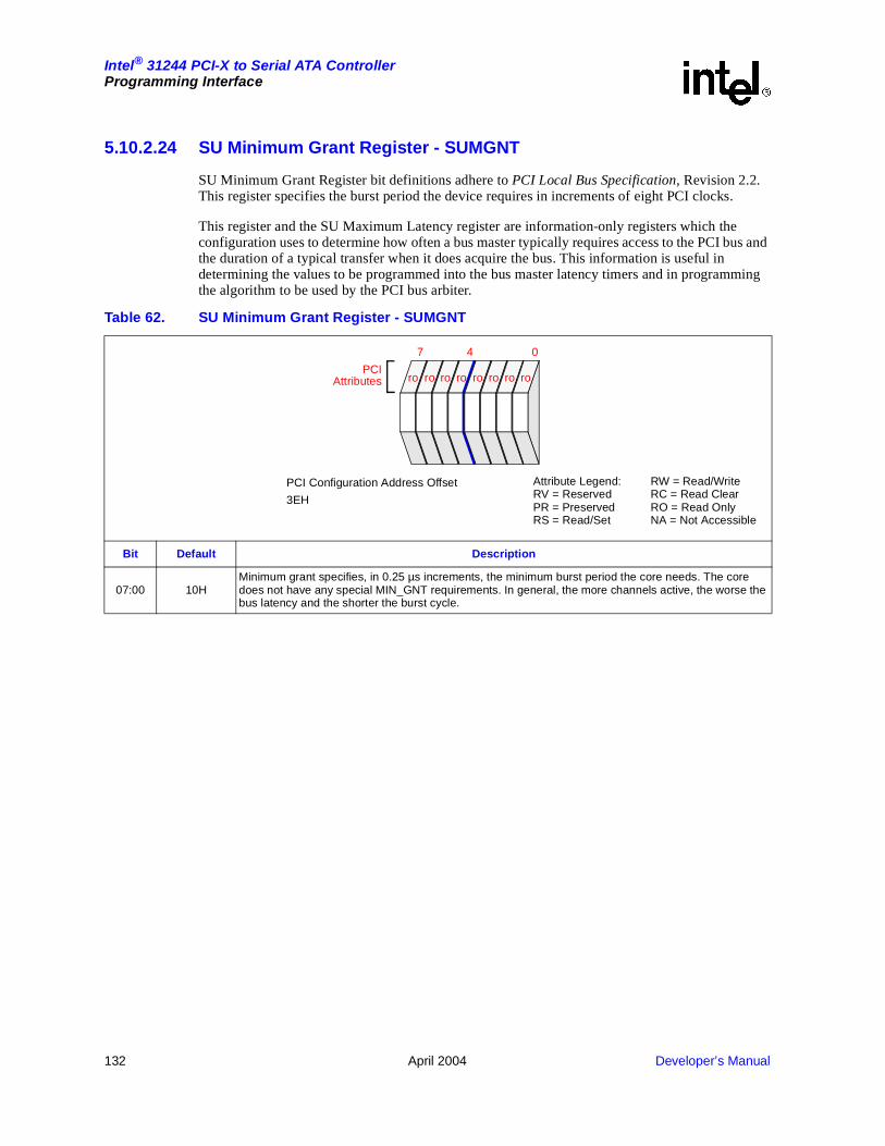
132 April 2004 Developer’s Manual
Intel® 31244 PCI-X to Serial ATA ControllerProgramming Interface
5.10.2.24 SU Minimum Grant Register - SUMGNT
SU Minimum Grant Register bit definitions adhere to PCI Local Bus Specification, Revision 2.2. This register specifies the burst period the device requires in increments of eight PCI clocks.
This register and the SU Maximum Latency register are information-only registers which the configuration uses to determine how often a bus master typically requires access to the PCI bus and the duration of a typical transfer when it does acquire the bus. This information is useful in determining the values to be programmed into the bus master latency timers and in programming the algorithm to be used by the PCI bus arbiter.
Table 62. SU Minimum Grant Register - SUMGNT
Bit Default Description
07:00 10HMinimum grant specifies, in 0.25 µs increments, the minimum burst period the core needs. The core does not have any special MIN_GNT requirements. In general, the more channels active, the worse the bus latency and the shorter the burst cycle.
PCIAttributes
7 4 0
ro ro ro ro ro ro ro ro
Attribute Legend:RV = ReservedPR = PreservedRS = Read/Set
RW = Read/WriteRC = Read ClearRO = Read OnlyNA = Not Accessible
PCI Configuration Address Offset
3EH
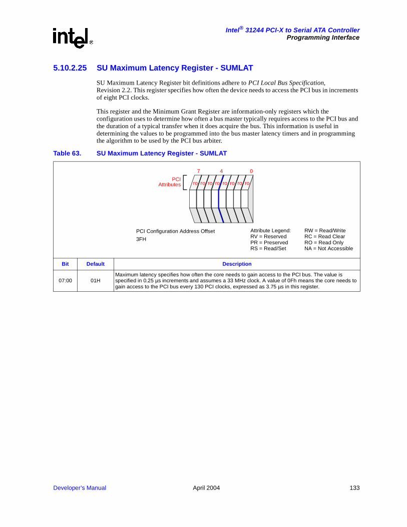
Developer’s Manual April 2004 133
Intel® 31244 PCI-X to Serial ATA ControllerProgramming Interface
5.10.2.25 SU Maximum Latency Register - SUMLAT
SU Maximum Latency Register bit definitions adhere to PCI Local Bus Specification, Revision 2.2. This register specifies how often the device needs to access the PCI bus in increments of eight PCI clocks.
This register and the Minimum Grant Register are information-only registers which the configuration uses to determine how often a bus master typically requires access to the PCI bus and the duration of a typical transfer when it does acquire the bus. This information is useful in determining the values to be programmed into the bus master latency timers and in programming the algorithm to be used by the PCI bus arbiter.
Table 63. SU Maximum Latency Register - SUMLAT
Bit Default Description
07:00 01HMaximum latency specifies how often the core needs to gain access to the PCI bus. The value is specified in 0.25 µs increments and assumes a 33 MHz clock. A value of 0Fh means the core needs to gain access to the PCI bus every 130 PCI clocks, expressed as 3.75 µs in this register.
PCIAttributes
7 4 0
ro ro ro ro ro ro ro ro
Attribute Legend:RV = ReservedPR = PreservedRS = Read/Set
RW = Read/WriteRC = Read ClearRO = Read OnlyNA = Not Accessible
PCI Configuration Address Offset
3FH

134 April 2004 Developer’s Manual
Intel® 31244 PCI-X to Serial ATA ControllerProgramming Interface
5.10.2.26 SPI Command Register - SPICMDR
Serial Peripheral Interface (SPI) Command Register definition is described in Table 64. The host writes the command type to the command register after setting up the control and data registers as necessary. A write to this register initiates the command.
Table 64. SPI Command Register - SPICMDR
Bit Default Description
7:0 00
Expansion Rom SPI interface command type. A write to this initiates the command. The status register bit D0 must be polled to determine when the command is complete.
06h = WREN (write enable)
04h = WRDI (write disable)
01h = WRSR (write status)
02h = No action (SPI PROGRAM command)
52h = SECT_ERASE (sector erase)
62h = CHIP_ERASE (all sector erase)
05h = RDSR (read status)
03h = No action (SPI READ command)
others = no action
PCIAttributes
7 4 0
rw rw rw rw rw rw rw rw
Attribute Legend:RV = ReservedPR = PreservedRS = Read/Set
RW = Read/WriteRC = Read ClearRO = Read OnlyNA = Not Accessible
PCI Configuration Address Offset
90

Developer’s Manual April 2004 135
Intel® 31244 PCI-X to Serial ATA ControllerProgramming Interface
5.10.2.27 SPI Control Register - SPICNTR
Serial Peripheral Interface (SPI) Control Register definition of this 8 bit register is described in Table 65. The host writes the control register to specify the sectors of the serial EEPROM to erase. Note that the set of all write pairs must be proceeded by one of the two erase commands with the sectors specified in the control register.
Table 65. SPI Control Register - SPICNTR
Bit Default Description
15:10 00h Reserved.
9:8 00b Sector address [1:0]. Selects 1 of 4 sectors for the sector erase command 52h. It must be set prior or simultaneously with writing the SECT_ERASE command to the SPI Command Register.
PCIAttributes
15 12 8
rv rv rv rv rv rv rw rw
Attribute Legend:RV = ReservedPR = PreservedRS = Read/Set
RW = Read/WriteRC = Read ClearRO = Read OnlyNA = Not Accessible
PCI Configuration Address Offset
91
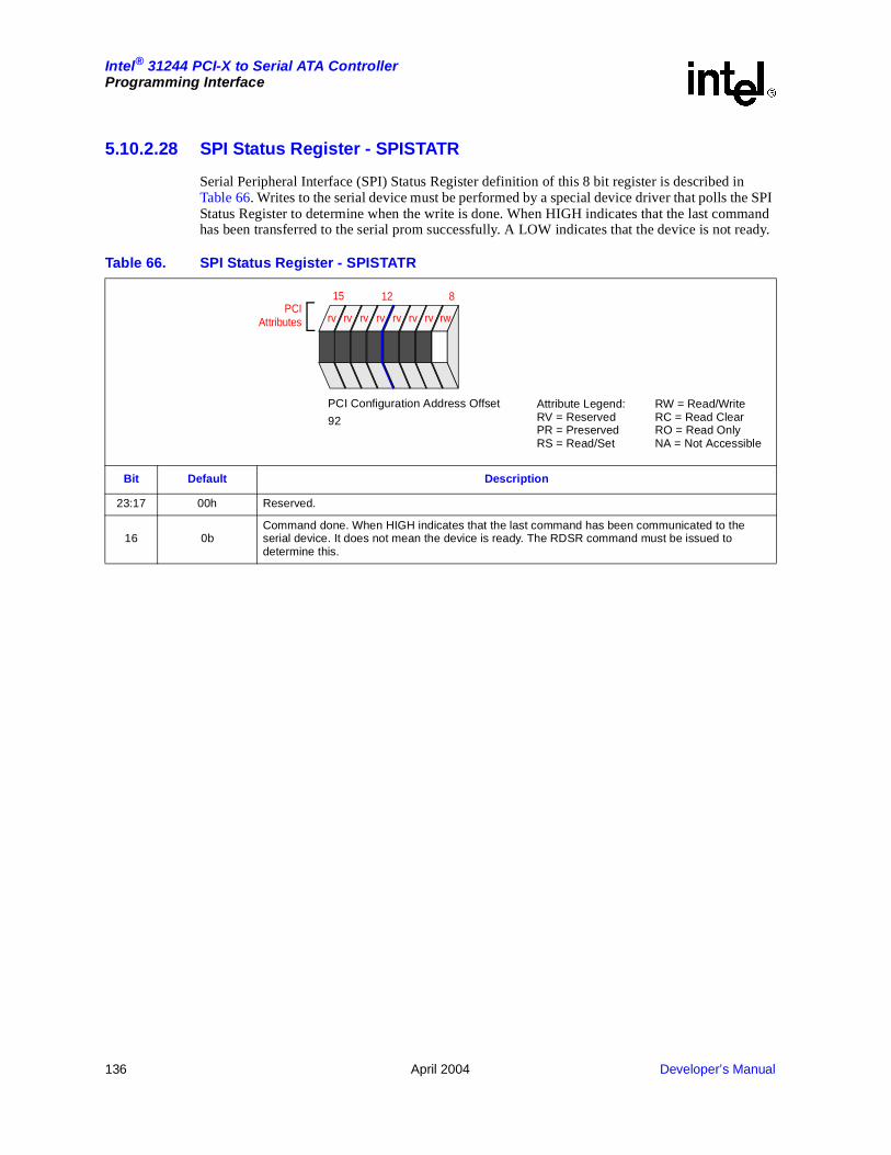
136 April 2004 Developer’s Manual
Intel® 31244 PCI-X to Serial ATA ControllerProgramming Interface
5.10.2.28 SPI Status Register - SPISTATR
Serial Peripheral Interface (SPI) Status Register definition of this 8 bit register is described in Table 66. Writes to the serial device must be performed by a special device driver that polls the SPI Status Register to determine when the write is done. When HIGH indicates that the last command has been transferred to the serial prom successfully. A LOW indicates that the device is not ready.
Table 66. SPI Status Register - SPISTATR
Bit Default Description
23:17 00h Reserved.
16 0bCommand done. When HIGH indicates that the last command has been communicated to the serial device. It does not mean the device is ready. The RDSR command must be issued to determine this.
PCIAttributes
15 12 8
rv rv rv rv rv rv rv rw
Attribute Legend:RV = ReservedPR = PreservedRS = Read/Set
RW = Read/WriteRC = Read ClearRO = Read OnlyNA = Not Accessible
PCI Configuration Address Offset
92

Developer’s Manual April 2004 137
Intel® 31244 PCI-X to Serial ATA ControllerProgramming Interface
5.10.2.29 SPI Data Register - SPIDATR
Serial Peripheral Interface (SPI) Data Register definition of this 32 bit register is described in Table 67. This is a multifunction register used by three commands. For the RDID command, it is a read-only register with manufacturer’s id and device id in the upper and lower bytes respectively. For the WRSR/RDSR commands, lower byte is a write/read register with the above bit definitions. WPEN is not applicable if the serial EEPROM device has its write protect pin WPB inactive high. Refer to the serial EEPROM device specification for how to use these bits.
Table 67. SPI Data Register - SPIDATR
Bit Default Description
31:16 0000h Reserved
15:8 00h Device ID for the RDID command.
7:0
This register contains data to be written to the EEPROM on a WRSR command and the data read from the EEPROM on RDSR and RDID commands. WRSR: Prior to a write of WRSR command to the SPI Command Register, this field should be written. Interpretation of these bits is as
follows:
7: WPEN - determines write protection state of the EEPROM with WEN
6: reserved, write as 0
5: reserved, write as 0
4: reserved, write as 0
3: BP1 - with BP0, selects the locked out sectors within the EEPROM.
2: BP0 - 00=No protection, 01=Sector 4 protected, 10=Sectors 3 & 4 protected, 11=All Sectors protected.
1: WEN - write as 0, this is a read-only bit in the EEPROM
0: RDY# - write as 0, this is a read-only bit in the EEPROM
RDSR: After completion of a RDSR command, this field contains the value of the EEPROMs Status Register. Interpretation of these bits is as follows:
7: WPEN - determines write protection state of the EEPROM with WEN
6: reserved, LOW when the EEPROM is not in an internal write cycle
5: reserved, LOW when the EEPROM is not in an internal write cycle
4: reserved, LOW when the EEPROM is not in an internal write cycle
3-2: BP1-BP0 selects which EEPROM sectors are protected. 00=No Protection, 01= Sector 4 is protected, 10=Sectors 3&4 are protected, 11=Sectors 1-4 are protected.
1: WEN - determines write protection state of the EEPROM with WPEN
0: RDY# -RDID: After completion of a RDID command, this field contains the 8-bit Manufacturer ID as read from the EEPROM. For the Atmel AT25F1024, this should be 1Fh.
PC
IA
ttribute
s 28 24 20 16 12 8 4 031
rv rv rv rv rv rv rv rv rv rv rv rv rv rv rv rv ro ro ro ro ro ro ro ro ro ro ro ro ro rorw
rorw
rorw rw rw rw rw rw
Attribute Legend:RV = ReservedPR = PreservedRS = Read/Set
RW = Read/WriteRC = Read ClearRO = Read OnlyNA = Not Accessible
PCI Configuration Address Offset
94

138 April 2004 Developer’s Manual
Intel® 31244 PCI-X to Serial ATA ControllerProgramming Interface
5.10.2.30 SU Extended Control and Status Register 0 - SUECSR0
This register is used to control the LED functionality and also to select the superset registers when in PCI IDE mode.
Table 68. SU Extended Control and Status Register 0 - SUECSR 0
Bit Default Description
31:29 0002 Reserved
28 12
LED0 Only:
• When this bit is set all SATA Ports’ activity are reflected on LED0 only. Other LEDs are not used.
• In PCI IDE mode, when this bit is cleared, LED0 reflects the activity for Channel 0 (Port 0 and Port 1) and LED1 reflects the activity for Channel 1 (Port 2 and Port 3).
• In DPA mode, when this bit is cleared, LED0, LED1, LED2, and LED3 reflect the activity for Port 0, Port 1, Port 2, and Port 3 respectively.
27:17 000H Reserved.
16 02
BAR 5 (Superset Features) Secondary Select:
• In PCI IDE mode this bit is a read/write bit and is used to select between the primary and secondary channel. When set, the secondary channel is selected.
• In DPA mode, this bit is a reserved bit.
15:03 02 Reserved.
02 02
Register protect.
• PCI IDE Mode: Register protect. Set this bit to 1 to enable writing the Device ID, Vendor ID, Class Code, Subclass Code, Interface Code registers and bits 27:24 and 1:0 of this register. Set to 0 to disable.
• DPA Mode: Register protect. Set this bit to 1 to enable writing the Device ID, Vendor ID, Class Code, Subclass Code, Interface Code registers and bits 27:24 and 1:0 of this register. Set to 0 to disable.
01 02
• PCI IDE Mode: PCI clock domain reset. Write a 1 to this register to reset the host Clk domain. Write a 0 for normal operation. This bit is write protected by setting bit 2 and write enabled by clearing bit 2.
• DPA Mode: PCI clock domain reset. Write a 1 to this register to reset the hostClk domain. Write a 0 for normal operation. This bit is write protected by setting bit 2 and write enabled by clearing bit 2.
00 02
• PCI IDE Mode: SATA clock domain reset. Write a 1 to this register to reset the sclk domain. Write a 0 for normal operation. This bit is write-protected by setting bit 2 and write enabled by clearing bit 2.
• DPA Mode: SATA clock domain reset. Write a 1 to this register to reset the sclk domain. Write a 0 for normal operation. This bit is write-protected by setting bit 2 and write enabled by clearing bit 2.
PCIAttributes
28 24 20 16 12 8 4 031
rv rv rv rw rv rv rv rv rv rv rv rv rv rv rv rw rv rv rv rv rv rv rv rv rv rv rv rv rv rw rw rw
Attribute Legend:RV = ReservedPR = PreservedRS = Read/Set
WO = Write Only
RW = Read/WriteRC = Read ClearRO = Read OnlyNA = Not Accessible
PCI Configuration Address Offset
98H - 9BH

Developer’s Manual April 2004 139
Intel® 31244 PCI-X to Serial ATA ControllerProgramming Interface
5.10.2.31 SU DMA Control Status Register- SUDCSCR
The control/status signals below are common to all four DMA channels or affect the Master Transaction Controller. Control/status signals that are individual to each port are contained in the Bus Master register set. See the description for the DMA Configuration register. Cache line alignment is enabled in the DMA write (from controller to memory) direction unless the Cache Line Size register is programmed with a value of 00h or an illegal value, in which case it is disabled. The burst length can only take values greater than the cache line size. If an illegal value is programmed for the burst length, the controller will internally use 40h for burst length, unless the cache line size is programmed for 80h, in which case the controller will use 80h. The burst length register is read/write and always returns the write value; if an illegal value is written, the corrected internal value will not be visible on read back. Cache line alignment is normally disabled in the DMA read direction. It may be enabled by setting bit 1.
Table 69. SU DMA Control Status Register - SUDCSCR 0
Bit Default Description
31:29 0002 Reserved
28 12 Reserved
27 1
When HIGH, enables resets to the PCI/PCI-X core master transaction queue when bit 19 of the PCI-X Capability Status register is cleared. This is necessary to recover from split responses that never get completed due to a corrupted tag. Bit 19 of the PCI-X Capability Status register may also be set by an unexpected split completion due to a corrupted requester ID for a split transaction that is not initiated by this master. Clearing the queue in this case will not hurt even though the queue will have been correct. For test purposes only; set only when there is no PCI traffic.
26:16 0 Reserved
15:08 80h
DMA Burst Length: Bus master transaction burst length: This register contains the DMA burst length value in [15:8]. This value sets the nominal PCI transaction burst length, other conditions permitting. The resolution is 1 DWORD so the maximum in each case is 512 bytes and the minimum is 32 bytes. The descriptor table defines the length of each physical region using physical region descriptors. The Controller transfers each physical region in individual burst transactions.
07:03 02 • Reserved.
02 02Block command disable. Set HIGH to disable the DMA engine from utilizing command types MWI and MRM in PCI mode only. This bit does not effect PCI-X mode.
01 02
DMA write cache align enable. When HIGH, the controller will align with the cacheline address before doing “burst length” transactions, total length permitting. When LOW, the controller will start with “burst length” transaction, regardless of start address, total length permitting.
00 02
DMA read cache align enable. When HIGH, the controller will align with the cacheline address before doing “burst length” transactions, total length permitting. When LOW, the controller will start with “burst length” transaction, regardless of start address, total length permitting.
PCIAttributes
28 24 20 16 12 8 4 031
rv rv rv rw rw rv rv rv rv rv rv rv rv rv rv rw rw rw rw rw rw rv rw rw rv rv rv rv rv rw rw rw
Attribute Legend:RV = ReservedPR = PreservedRS = Read/Set
WO = Write Only
RW = Read/WriteRC = Read ClearRO = Read OnlyNA = Not Accessible
PCI Configuration Address Offset
A0H - A3H

140 April 2004 Developer’s Manual
Intel® 31244 PCI-X to Serial ATA ControllerProgramming Interface
5.10.2.32 SU Dummy Register SUDR
SU Dummy Register SUDR contains dummy Bits for scratchpad read/write.
Table 70. SU Dummy Register - SUDR
Bit Default Description
31:00 0000_0000h Dummy bits for scratch pad reads and writes.
PC
IA
ttribute
s 28 24 20 16 12 8 4 031
rw rw rw rw rw rw rw rw rw rw rw rw rw rw rw rw rw rw rw rw rw rw rw rw rw rw rw rw rw rw rw rw
Attribute Legend:RV = ReservedPR = PreservedRS = Read/Set
RW = Read/WriteRC = Read ClearRO = Read OnlyNA = Not Accessible
PCI Configuration Address Offset
A4 - A7

Developer’s Manual April 2004 141
Intel® 31244 PCI-X to Serial ATA ControllerProgramming Interface
5.10.2.33 SU Interrupt Status Register SUISR
This register reports interrupts generated by the SATA ports. Software must clear any pending interrupt at the appropriate sources. The IDE interrupts (bits 31, 23, 15, 7) are cleared by reading the SATA Port Command Block Status register. Other pending interrupts in this register are generated by the Superset Error registers and must be cleared by writing 1s to the Superset Error registers. These registers located in configuration space for PCI IDE mode and in the memory space for DPA mode.
Table 71. SU Interrupt Status Register - SUISR
Bit Default PCI IDE Description
31:24 0 Port 4 Interrupt Status. Same as bits 7:0 corresponding to Port 4
23:16 0 Port 3 Interrupt Status. Same as bits 7:0 corresponding to Port 3
15:8 0 Port 2 Interrupt Status. Same as bits 7:0 corresponding to Port 3
7 0 Port 1 ATA Interrupt
6 0 Port 1 CRC Error. This is the latched CRC error from the previous data transfer.
5 0 Port 1 Data Integrity Error. A CRC or disparity error was detected by the host, or an RERR was returned by the device in response to a data FIS transfer.
4 0 Port 1 Unrecognized FIS Reception. An unrecognized FIS type was received.
3 0 Port 1 RERR Received. An RERR was received in response to a data transfer.
2 0 Port 1 FIFO Error. A FIFO error occurred during a data FIS transfer
1 0 Port 1 PHY went from Not-Ready to Ready steady state. The PHY became ready and OOB was completed.
0 0 Port 1 PHY Ready Change-Of-State. The PHY went from Ready to Not Ready or from Not-Read to Ready.
PCI DPA Mode Description
31:00 0000_0000 Reserved - Note: Bits are Read Only in DPA mode
PC
IA
ttribute
s 28 24 20 16 12 8 4 031
rw rw rw rw rw rw rw rw rw rw rw rw rw rw rw rw rw rw rw rw rw rw rw rw rw rw rw rw rw rw rw rw
Attribute Legend:RV = ReservedPR = PreservedRS = Read/Set
RW = Read/WriteRC = Read ClearRO = Read OnlyNA = Not Accessible
PCI Configuration Address Offset
A8-AB PCI IDE

142 April 2004 Developer’s Manual
Intel® 31244 PCI-X to Serial ATA ControllerProgramming Interface
5.10.2.34 SU Interrupt Mask Register SUIMR
This register masks interrupts pending in the Interrupt Pending register. Each bit in the Interrupt Mask register corresponds to a bit in the Interrupt Pending register. Writing a one to a bit in this register enables the interrupt source bit. These registers located in configuration space in PCI IDE mode and in the common space in DPA mode. These registers are located in configuration space for PCI IDE mode and in the memory space for DPA mode.
Table 72. SU Interrupt Mask Register - SUIMR
Bit Default PCI IDE Description
31:24 0 Port 4 Interrupt Mask. Same as bits 7:0 corresponding to Port 4
23:16 0 Port 3 Interrupt Mask. Same as bits 7:0 corresponding to Port 3
15:8 0 Port 2 Interrupt Masks. Same as bits 7:0 corresponding to Port 3
7 0 Port 1 Interrupt Mask - when high enables Port 1 CRC Interrupts. When low Port 1 CRC Interrupts are disabled.
6 0 When high enables Port 1 CRC Error to generate and interrupt. When low this interrupt source is re disabled.
5 0 When high enables Port 1 Data Integrity Error to generate and interrupt. When low this interrupt source is disabled.
4 0 When high enables Port 1 Unrecognized FIS Reception Error to generate and interrupt. When low this interrupt source is disabled
3 0 When high enables Port 1 RERR Received Error to generate and interrupt. When low this interrupt source is disabled
2 0 When high enables Port 1 FIFO Error to generate and interrupt. When low this interrupt source is disabled
1 0 When high enables Port 1 Going Ready to generate and interrupt. When low this interrupt source is disabled.
0 0 When high enables Port 1 Going Ready to generate and interrupt. When low this interrupt source is disabled.
PCI DPA Mode Description
31:00 0000_0000 Reserved
PC
IA
ttribute
s 28 24 20 16 12 8 4 031
rw rw rw rw rw rw rw rw rw rw rw rw rw rw rw rw rw rw rw rw rw rw rw rw rw rw rw rw rw rw rw rw
Attribute Legend:RV = ReservedPR = PreservedRS = Read/Set
RW = Read/WriteRC = Read ClearRO = Read OnlyNA = Not Accessible
PCI Configuration Address Offset
AC-AFH PCI IDE

Developer’s Manual April 2004 143
Intel® 31244 PCI-X to Serial ATA ControllerProgramming Interface
5.10.2.35 SU Transaction Control SUTCR
This register provides primary transaction control. The bits in the register should be set at reset values only.
Table 73. SU Transaction Control Register - SUTCR
Bit Default Description
31 0 Target read delayed transaction for I/O and non-prefetchable regions discarded. Write 1 to clear.
30 0 Target read delayed transaction for all regions discarded. Write 1 to clear.
29 0 Target (I/O and memory) read delayed/split at time out/immediately (default time out)
28 0 Target (I/O and memory) read delayed/split at time out/immediately (default time out)
27 0
Target (I/O and memory) read delayed /split or retry select (if application interface is not ready)
0 = delayed/split transaction
1 = retry transaction (always immediate retry, no AT_REQ to application)
26 0 Target (I/O and memory) read target abort enable (if application interface is not ready at the latency time out)
25 0 Target (I/O) write split enable (at time out/immediately; default time out)
24 0 Target (I/O) write split enable (if application interface is not ready)
23 0 Target (read/write) master abort enable; check at the start of each transaction.
22:20 0h Target subsequent latency time out enable: 0 = 8, 1 to 7.
19:16 0 Target initial latency time-out in PCI mode: 0= 16, 8 to 15
15:4 000h Programmable boundary enable to disconnect/prefetch for target burst read cycles to prefetchable region in PCI. A value of 1 indicates end of boundary (64KB down to 16 bytes).
3 0Disconnect/prefetch to prefetchable memory regions enable. Prefetchable memory regions are always disconnected on a region boundary. Non-prefetchable regions for PCI are always disconnected on the first transfer.
2 0 Reserved
1 0
Target split write control
0 = blocks all requests except PMW
1 = blocks all requests including PMW until split completion occurs.
0 0 cr_lat_timer_disable
PC
IA
ttribute
s 28 24 20 16 12 8 4 031
rw rw rw rw rw rw rw rw rw rw rw rw rw rw rw rw rw rw rw rw rw rw rw rw rw rw rw rw rw rw rw rw
Attribute Legend:RV = ReservedPR = PreservedRS = Read/Set
RW = Read/WriteRC = Read ClearRO = Read OnlyNA = Not Accessible
PCI Configuration Address Offset
C0-C3

144 April 2004 Developer’s Manual
Intel® 31244 PCI-X to Serial ATA ControllerProgramming Interface
5.10.2.36 SU Target Split Completion Message Enable Register SUTSCMER
This register contains any split completion error messages received (SCM bit = 1 and SCE bit = 1). Bit 29 of the PCI configuration Status Register is set when a split completion error message is received.
Table 74. SU Target Split Completion Message Enable Register- SUTSCMER
Bit Default Description
31:0 0 Target read delayed transaction for I/O and non-prefetchable regions discarded. Write 1 to clear.
PC
IA
ttribute
s 28 24 20 16 12 8 4 031
rw rw rw rw rw rw rw rw rw rw rw rw rw rw rw rw rw rw rw rw rw rw rw rw rw rw rw rw rw rw rw rw
Attribute Legend:RV = ReservedPR = PreservedRS = Read/Set
RW = Read/WriteRC = Read ClearRO = Read OnlyNA = Not Accessible
PCI Configuration Address Offset
C4-C7
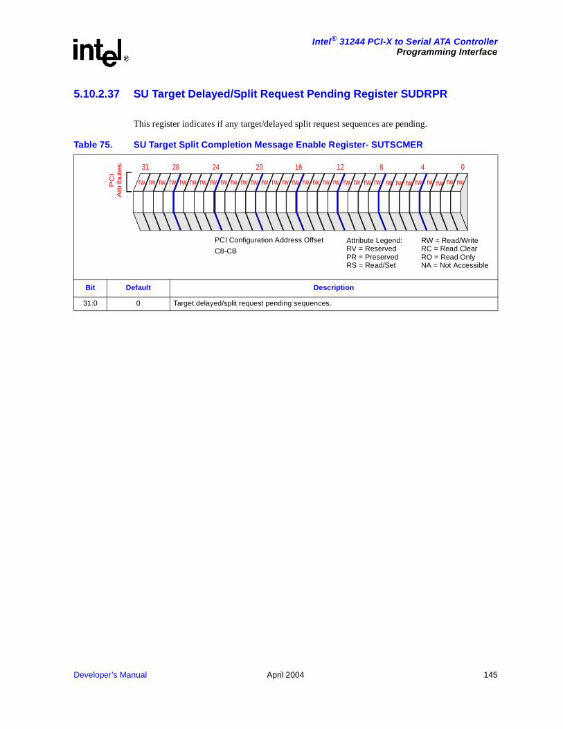
Developer’s Manual April 2004 145
Intel® 31244 PCI-X to Serial ATA ControllerProgramming Interface
5.10.2.37 SU Target Delayed/Split Request Pending Register SUDRPR
This register indicates if any target/delayed split request sequences are pending.
Table 75. SU Target Split Completion Message Enable Register- SUTSCMER
Bit Default Description
31:0 0 Target delayed/split request pending sequences.
PC
IA
ttribute
s 28 24 20 16 12 8 4 031
rw rw rw rw rw rw rw rw rw rw rw rw rw rw rw rw rw rw rw rw rw rw rw rw rw rw rw rw rw rw rw rw
Attribute Legend:RV = ReservedPR = PreservedRS = Read/Set
RW = Read/WriteRC = Read ClearRO = Read OnlyNA = Not Accessible
PCI Configuration Address Offset
C8-CB
146 April 2004 Developer’s Manual
Intel® 31244 PCI-X to Serial ATA ControllerProgramming Interface
5.10.2.38 SU Transaction Control 2 Register SUTC2R
This register provides secondary transaction control.
Table 76. SU Transaction Control 2 Register- SUTC2R
Bit Default Description
31 1
Master request (memory read) byte count/byte enable select.
• 0 = Byte enables valid. In PCI mode, a burst transaction cannot be performed using memory read command 6h.
• 1 = DWORD byte count valid (default). In PCI mode, the memory read byte enables are automatically generated by the core.
30 0
Master request (I/O and CR cycles) byte count/byte enable select.
• 0 = Byte enables valid
• 1 = DWORD byte count valid.
29 0
Master (retry) deferred write enable (allows read requests to pass).
PCI mode I/O and memory transactions only.
• 0 = New read requests are not accepted until the current write cycle completes. Reads cannot pass writes.
• 1 = New read requests are accepted, even when there is a write cycle pending. Reads can pass writes.
28 0
Master (retry) deferred read enable (allows read/write requests to pass.) PCI mode I/O and memory transactions only.
• 0 = New read/write requests are not accepted until the current read cycle completes. Read/Write requests cannot pass reads.
• 1 = New read/write requests are accepted, even when there is a read cycle pending. Read/write requests can pas reads.
27 0
Master I/O deferred/split request outstanding maximum count
• 0 =CCh[26:24]
• 1 = 1
PC
IA
ttribute
s 28 24 20 16 12 8 4 031
rw rw rw rw rw rw rw rw ro ro ro ro ro ro ro ro ro ro rw rw rw rw rw rw rw rw rw rw rw rw rw rw
Attribute Legend:RV = ReservedPR = PreservedRS = Read/Set
RW = Read/WriteRC = Read ClearRO = Read OnlyNA = Not Accessible
PCI Configuration Address Offset
CC-CF
Developer’s Manual April 2004 147
Intel® 31244 PCI-X to Serial ATA ControllerProgramming Interface
26:24 010b
Master deferred read request outstanding max count. PCI mode only.
Bits 26:24=000b, Max# SAC Cycles=8, Max# DAC Cycles=4
Bits 26:24=001b, Max# SAC Cycles=1, Max# DAC Cycles=0
Bits 26:24=010b, Max# SAC Cycles=2, Max# DAC Cycles=1
Bits 26:24=011b, Max# SAC Cycles=3, Max# DAC Cycles=1
Bits 26:24=100b, Max# SAC Cycles=4, Max# DAC Cycles=2
Bits 26:24=101b, Max# SAC Cycles=5, Max# DAC Cycles=2
Bits 26:24=110b, Max# SAC Cycles=6, Max# DAC Cycles=3
Bits 26:24=111b, Max# SAC Cycles=7, Max# DAC Cycles=3
For the PCI-X maximum outstanding split transactions, refer to crE0[22:20].
23:16 0000000b Target/master error sequence number.
15 0
Target error command indication
0 = delayed/split
1 = others.
14 0
Target/master error indication
0 = target
1 = master
13 0 Target/master system error. This bit is set whenever ATM_SERR_O is active. Write one to clear.
12 0 Target/master data PERR# error status. This bit is set whenever ATM_DATA_PERR_O is active. Write one to clear.
11 0 Target/master address PERR# error status. This bit is set whenever ATM_ADD_PERR_O is active. Write one to clear.
10:9 00 Reserved.
8 0Target illegal I/O DWORD byte combinations detected. Write one to
clear.
7 0Target illegal I/O DWORD byte detection ENABLE. Allows error to set
SERR if SERR is enabled, also sets bit 8 above.
6 0 Reserved
5 0
Target I/O delayed split request outstanding maximum count:
0 = CCh[4:0]
1 = 1.
4:0 0001 Target delayed/split request outstanding maximum count: 0 = 32, 1 to 31.
Table 76. SU Transaction Control 2 Register- SUTC2R
Bit Default Description
PC
IA
ttribute
s 28 24 20 16 12 8 4 031
rw rw rw rw rw rw rw rw ro ro ro ro ro ro ro ro ro ro rw rw rw rw rw rw rw rw rw rw rw rw rw rw
Attribute Legend:RV = ReservedPR = PreservedRS = Read/Set
RW = Read/WriteRC = Read ClearRO = Read OnlyNA = Not Accessible
PCI Configuration Address Offset
CC-CF
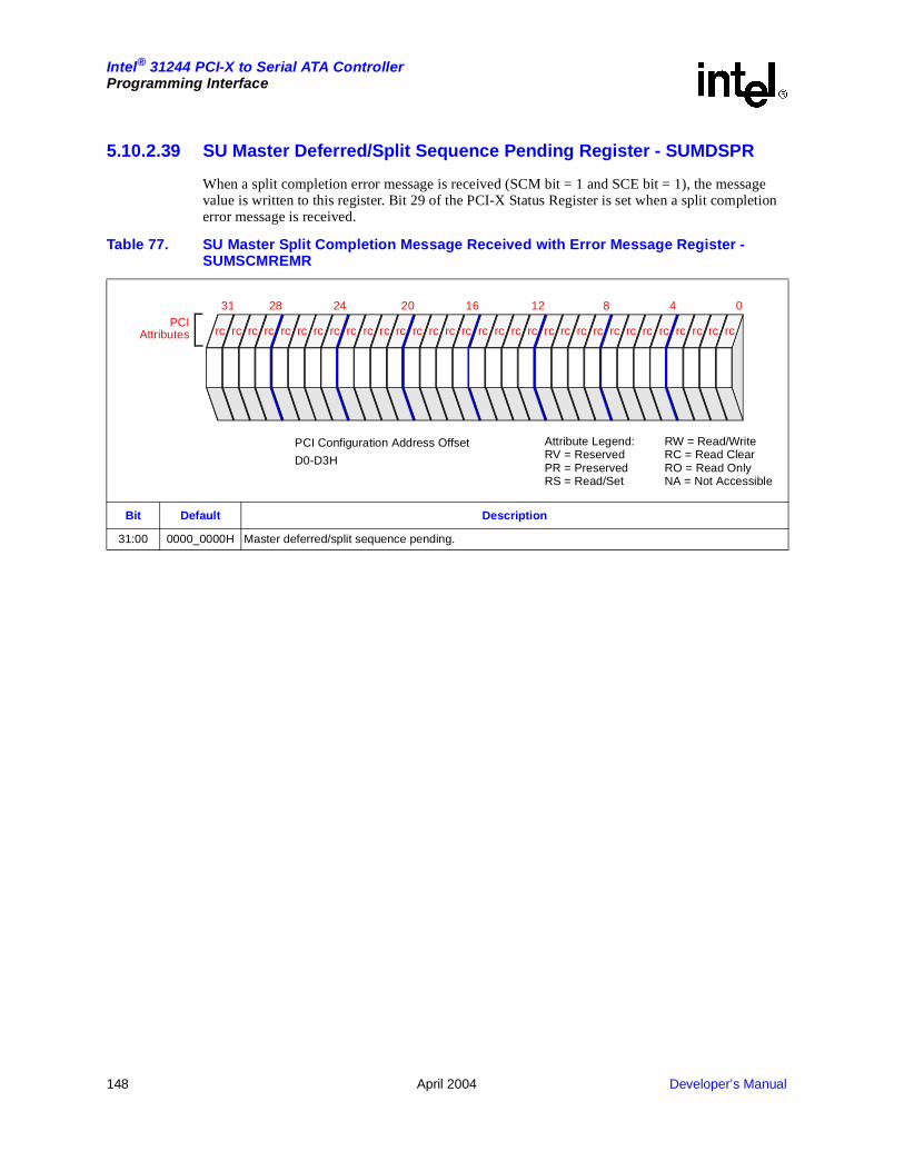
148 April 2004 Developer’s Manual
Intel® 31244 PCI-X to Serial ATA ControllerProgramming Interface
5.10.2.39 SU Master Deferred/Split Sequence Pending Register - SUMDSPR
When a split completion error message is received (SCM bit = 1 and SCE bit = 1), the message value is written to this register. Bit 29 of the PCI-X Status Register is set when a split completion error message is received.
Table 77. SU Master Split Completion Message Received with Error Message Register -SUMSCMREMR
Bit Default Description
31:00 0000_0000H Master deferred/split sequence pending.
PCIAttributes
28 24 20 16 12 8 4 031
rc rc rc rc rc rc rc rc rc rc rc rc rc rc rc rc rc rc rc rc rc rc rc rc rc rc rc rc rc rc rc rc
Attribute Legend:RV = ReservedPR = PreservedRS = Read/Set
RW = Read/WriteRC = Read ClearRO = Read OnlyNA = Not Accessible
PCI Configuration Address Offset
D0-D3H

Developer’s Manual April 2004 149
Intel® 31244 PCI-X to Serial ATA ControllerProgramming Interface
5.10.2.40 SU Master Split Completion Message Receivedwith Error Message Register - SUMSCMREMR
When a split completion error message is received (SCM bit = 1 and SCE bit = 1), the message value is written to this register. Bit 29 of the PCI-X Status Register is set when a split completion error message is received.
Table 78. SU Master Split Completion Message Received with Error Message Register -SUMSCMREMR
Bit Default Description
31:00 0000_0000HSplit Completion Error Message Value - When a split completion error message (SCM bit = 1 and SCE bit = 1) is received, the message value is written into this register. This register is cleared by writing 1s to all bits.
PCIAttributes
28 24 20 16 12 8 4 031
rc rc rc rc rc rc rc rc rc rc rc rc rc rc rc rc rc rc rc rc rc rc rc rc rc rc rc rc rc rc rc rc
Attribute Legend:RV = ReservedPR = PreservedRS = Read/Set
RW = Read/WriteRC = Read ClearRO = Read OnlyNA = Not Accessible
PCI Configuration Address Offset
D4H - D7H

150 April 2004 Developer’s Manual
Intel® 31244 PCI-X to Serial ATA ControllerProgramming Interface
5.10.2.41 SU Arbiter Control - SUACR
This register provides master arbiter control.
Table 79. SU Arbiter Control Register SUACR
Bit Default Description
31:30 00b
Master arbiter control, MSI Request.Used only for Fixed Priority (bit 25 set to 1).
00 = Highest priority
01 = Medium priority
10 = Lowest priority
00 = Reserved
29:28 00b
Master arbiter control, Target Split Completion. Used only for Fixed Priority (bit 25 set to 1).
00 = Highest priority
01 = Medium priority
10 = Lowest priority
00 = Reserved
27:26 00b
Target Split Completion, New Request, Deferred Read, Deferred Write. Used only for Fixed Priority (bit
25 set to 1).
00 = Highest priority
01 = Medium priority
10 = Lowest priority
00 = Reserved
25 0
Fixed/Round Robin priority selector.
1 = Fixed
0 = Round Robin
24:18 0000000b Reserved
17 0 Master retry aborted. Write one to clear.
16 0 Master TRDY time out aborted. Write one to clear.
15:8 0
Master retry value:
0 = infinite
1 to FFh.
7:0 00h
Master TRDY time out value:
0 = disabled
1 to FFh.
PCIAttributes
28 24 20 16 12 8 4 031
rw rw rw rw rw rw rw ro ro ro ro ro ro ro rw rw rw rw rw rw rw rw rw rw rw rw rw rw rw rw rw rw
Attribute Legend:RV = ReservedPR = PreservedRS = Read/Set
RW = Read/WriteRC = Read ClearRO = Read OnlyNA = Not Accessible
PCI Configuration Address Offset
D8 - DC

Developer’s Manual April 2004 151
Intel® 31244 PCI-X to Serial ATA ControllerProgramming Interface
5.10.2.42 SU PCI-X Capability Identifier Register - SUPCI-X_Cap_ID
The Capability Identifier Register bits adhere to the definitions in the PCI Local Bus Specification, Revision 2.2. This register in the PCI Extended Capability header identifies the type of Extended Capability contained in that header. In the case of the GD31244 controller, this is the PCI-X extended capability with an ID of 07H as defined by the PCI-X Addendum to the PCI Local Bus Specification, Revision 1.0a.
Table 80. SU PCI-X_Capability Identifier Register - SUPCI-X_Cap_ID
Bit Default Description
07:00 07H Cap_Id - This field with its’ 07H value identifies this item in the linked list of Extended Capability Headers as being the PCI-X capability registers.
PCIAttributes
7 4 0
ro ro ro ro ro ro ro ro
Attribute Legend:RV = ReservedPR = PreservedRS = Read/Set
RW = Read/WriteRC = Read ClearRO = Read OnlyNA = Not Accessible
PCI Configuration Offset
E0H

152 April 2004 Developer’s Manual
Intel® 31244 PCI-X to Serial ATA ControllerProgramming Interface
5.10.2.43 SU PCI-X Next Item Pointer Register - SUPCI-X_Next_Item_Ptr
The Next Item Pointer Register bits adhere to the definitions in the PCI Local Bus Specification, Revision 2.2. This register describes the location of the next item in the function capability list. For the GD31244 controller, the next capability (PM capability list) is located at off-set E8H.
Table 81. SU PCI-X Next Item Pointer Register - SUPCI-X_Next_Item_Ptr
Bit Default Description
07:00 E8H Next_ Item_ Pointer - This field provides an offset into the function configuration space pointing to the next item in the function capability list which is the PM capability header residing at E8H.
PCIAttributes
7 4 0
ro ro ro ro ro ro ro ro
Attribute Legend:RV = ReservedPR = PreservedRS = Read/Set
RW = Read/WriteRC = Read ClearRO = Read OnlyNA = Not Accessible
PCI Configuration Offset
E1H
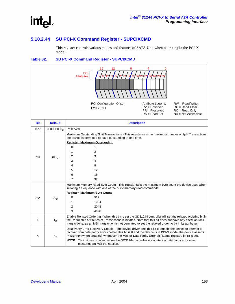
Developer’s Manual April 2004 153
Intel® 31244 PCI-X to Serial ATA ControllerProgramming Interface
5.10.2.44 SU PCI-X Command Register - SUPCIXCMD
This register controls various modes and features of SATA Unit when operating in the PCI-X mode.
Table 82. SU PCI-X Command Register - SUPCIXCMD
Bit Default Description
15:7 0000000002 Reserved.
6:4 0112
Maximum Outstanding Split Transactions - This register sets the maximum number of Split Transactions the device is permitted to have outstanding at one time.
Register Maximum Outstanding
0 1
1 2
2 3
3 4
4 8
5 12
6 16
7 32
3:2 002
Maximum Memory Read Byte Count - This register sets the maximum byte count the device uses when initiating a Sequence with one of the burst memory read commands.
Register Maximum Byte Count
0 512
1 1024
2 2048
3 4096
1 12
Enable Relaxed Ordering - When this bit is set the GD31244 controller will set the relaxed ordering bit in the Requester Attributes of Transactions it initiates. Note that this bit does not have any effect on MSI transactions, as an MSI transaction is not permitted to set the relaxed ordering bit in its attributes.
0 02
Data Parity Error Recovery Enable - The device driver sets this bit to enable the device to attempt to recover from data parity errors. When this bit is 0 and the device is in PCI-X mode, the device asserts P_SERR# (when enabled) whenever the Master Data Parity Error bit (Status register, bit 8) is set.
NOTE: This bit has no effect when the GD31244 controller encounters a data parity error when mastering an MSI transaction.
PCIAttributes
15 12 8 4 0
rv rv rv rv rv rv rv rv rv rw rw rw rw rw rw rw
Attribute Legend:RV = ReservedPR = PreservedRS = Read/Set
RW = Read/WriteRC = Read ClearRO = Read OnlyNA = Not Accessible
PCI Configuration Offset
E2H - E3H

154 April 2004 Developer’s Manual
Intel® 31244 PCI-X to Serial ATA ControllerProgramming Interface
5.10.2.45 SU PCI-X Status Register - SUPCIXSR
This register identifies the capabilities and current operating mode of SATA Unit when operating in the PCI-X mode.
Table 83. SU PCI-X Status Register - SUPCIXSR (Sheet 1 of 2)
Bit Default Description
31:30 002 Reserved
29 02
Received Split Completion Error Message - This bit is set when the device receives a Split Completion Message with the Split Completion Error attribute bit set. Once set, this bit remains set until software writes a 1 to this location.
0 = No Split Completion error message received.1 = A Split Completion error message has been received.
28:26 0012
Designed Maximum Cumulative Read Size (DMCRS) - The value of this register depends on the setting of the Maximum Memory Read Byte Count field of the PCIXCMD register:
DMCRS Max ADQs Maximum Memory Read Byte Count Register Setting
1 16 512 (Default)2 32 10242 32 20482 32 4096
25:23 0112Designed Maximum Outstanding Split Transactions - The GD31244 controller may have up to four outstanding split transactions.
22:21 002Designed Maximum Memory Read Byte Count - The GD31244 controller may generate memory reads with byte counts up to 512 bytes.
20 02
Device Complexity - GD31244 controller is a simple device.
0 = Simple1 = Complex
19 02
Unexpected Split Completion - This bit is set when an unexpected Split Completion with this device Requester ID is received. Once set, this bit remains set until software writes a 1 to this location.
0 = No unexpected Split Completion has been received.1 = An unexpected Split Completion has been received.
18 02
Split Completion Discarded - This bit is set when the device discards a Split Completion because the requester does not accept it. See Section 5.4.4 of the PCI-X Addendum to the PCI Local Bus Specification, Revision 1.0a for details. Once set, this bit remains set until software writes a 1 to this location.
0 = No Split Completion has been discarded.1 = A Split Completion has been discarded.
NOTE: The GD31244 controller will not set this bit since there is no Inbound address responding to Inbound Read Requests with Split Responses (Memory or Register) that has “read side effects.”
17 12 GD31244 controller is a 133 MHz capable device.
PCIAttributes
28 24 20 16 12 8 4 031
rv rv rc ro ro ro ro ro ro ro ro ro rc ro ro ro ro ro ro ro ro ro ro ro ro ro ro ro ro ro ro ro
Attribute Legend:RV = ReservedPR = PreservedRS = Read/Set
RW = Read/WriteRC = Read ClearRO = Read OnlyNA = Not Accessible
PCI Configuration Offset
E4H-E7H

Developer’s Manual April 2004 155
Intel® 31244 PCI-X to Serial ATA ControllerProgramming Interface
16 32BITPCI#
The GD31244 controller may be configured to identify the add-in card to the system as 64-bit or 32-bit wide through a user-configurable strap (32BITPCI#). This strap will by default identify the GD31244 controller subsystem as 64-bit unless the user attaches the appropriate pull-down resistor to the strap.
0 = The bus is 32 bits wide.1 = The bus is 64 bits wide.
15:8 FFH
Bus Number - This register is read for diagnostic purposes only. It indicates the number of the bus segment for the device containing this function. The function uses this number as part of its Requester ID and Completer ID. For all devices other than the source bridge, each time the function is addressed by a Configuration Write transaction, the function must update this register with the contents of AD[7:0] of the attribute phase of the Configuration Write, regardless of which register in the function is addressed by the transaction. The function is addressed by a Configuration Write transaction when all of the following are true:
1. The transaction uses a Configuration Write command.2. IDSEL is asserted during the address phase.3. AD[1:0] are 00b (Type 0 configuration transaction).4. AD[10:08] of the configuration address contain the appropriate function number.
7:3 1FH
Device Number - This register is read for diagnostic purposes only. It indicates the number of the device containing this function, i.e., the number in the Device Number field (AD[15:11]) of the address of a Type 0 configuration transaction that is assigned to the device containing this function by the connection of the system hardware. The system must assign a device number other than 00h (00h is reserved for the source bridge). The function uses this number as part of its Requester ID and Completer ID. Each time the function is addressed by a Configuration Write transaction, the device must update this register with the contents of AD[15:11] of the address phase of the Configuration Write, regardless of which register in the function is addressed by the transaction. The function is addressed by a Configuration Write transaction when all of the following are true:
1. The transaction uses a Configuration Write command.2. IDSEL is asserted during the address phase.3. AD[1:0] are 00b (Type 0 configuration transaction).4. AD[10:08] of the configuration address contain the appropriate function number.
2:0 0002
Function Number - This register is read for diagnostic purposes only. It indicates the number of this function; i.e., the number in the Function Number field (AD[10:08]) of the address of a Type 0 configuration transaction to which this function responds. The function uses this number as part of its Requester ID and Completer ID.
Table 83. SU PCI-X Status Register - SUPCIXSR (Sheet 2 of 2)
Bit Default Description
PCIAttributes
28 24 20 16 12 8 4 031
rv rv rc ro ro ro ro ro ro ro ro ro rc ro ro ro ro ro ro ro ro ro ro ro ro ro ro ro ro ro ro ro
Attribute Legend:RV = ReservedPR = PreservedRS = Read/Set
RW = Read/WriteRC = Read ClearRO = Read OnlyNA = Not Accessible
PCI Configuration Offset
E4H-E7H
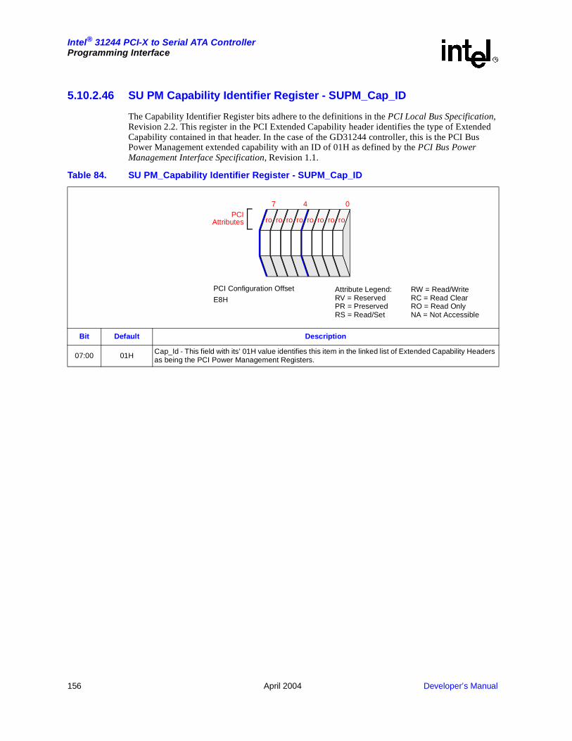
156 April 2004 Developer’s Manual
Intel® 31244 PCI-X to Serial ATA ControllerProgramming Interface
5.10.2.46 SU PM Capability Identifier Register - SUPM_Cap_ID
The Capability Identifier Register bits adhere to the definitions in the PCI Local Bus Specification, Revision 2.2. This register in the PCI Extended Capability header identifies the type of Extended Capability contained in that header. In the case of the GD31244 controller, this is the PCI Bus Power Management extended capability with an ID of 01H as defined by the PCI Bus Power Management Interface Specification, Revision 1.1.
Table 84. SU PM_Capability Identifier Register - SUPM_Cap_ID
Bit Default Description
07:00 01H Cap_Id - This field with its’ 01H value identifies this item in the linked list of Extended Capability Headers as being the PCI Power Management Registers.
PCIAttributes
7 4 0
ro ro ro ro ro ro ro ro
Attribute Legend:RV = ReservedPR = PreservedRS = Read/Set
RW = Read/WriteRC = Read ClearRO = Read OnlyNA = Not Accessible
PCI Configuration Offset
E8H
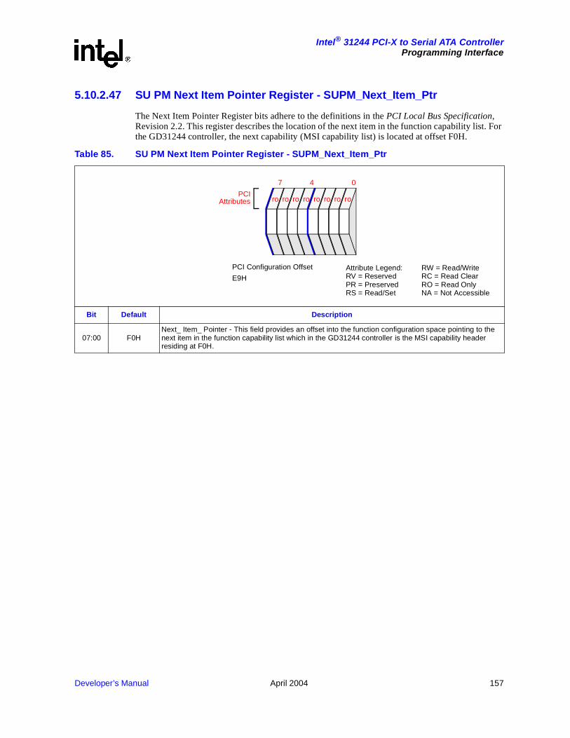
Developer’s Manual April 2004 157
Intel® 31244 PCI-X to Serial ATA ControllerProgramming Interface
5.10.2.47 SU PM Next Item Pointer Register - SUPM_Next_Item_Ptr
The Next Item Pointer Register bits adhere to the definitions in the PCI Local Bus Specification, Revision 2.2. This register describes the location of the next item in the function capability list. For the GD31244 controller, the next capability (MSI capability list) is located at offset F0H.
Table 85. SU PM Next Item Pointer Register - SUPM_Next_Item_Ptr
Bit Default Description
07:00 F0HNext_ Item_ Pointer - This field provides an offset into the function configuration space pointing to the next item in the function capability list which in the GD31244 controller is the MSI capability header residing at F0H.
PCIAttributes
7 4 0
ro ro ro ro ro ro ro ro
Attribute Legend:RV = ReservedPR = PreservedRS = Read/Set
RW = Read/WriteRC = Read ClearRO = Read OnlyNA = Not Accessible
PCI Configuration Offset
E9H
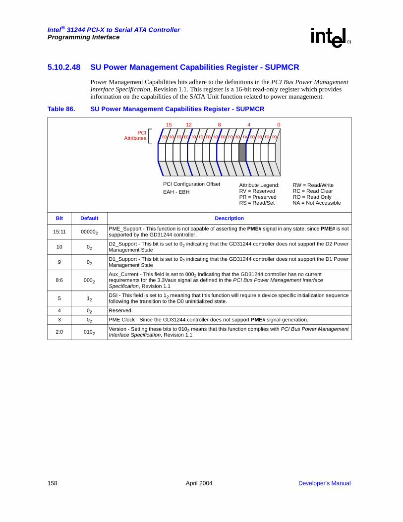
158 April 2004 Developer’s Manual
Intel® 31244 PCI-X to Serial ATA ControllerProgramming Interface
5.10.2.48 SU Power Management Capabilities Register - SUPMCR
Power Management Capabilities bits adhere to the definitions in the PCI Bus Power Management Interface Specification, Revision 1.1. This register is a 16-bit read-only register which provides information on the capabilities of the SATA Unit function related to power management.
Table 86. SU Power Management Capabilities Register - SUPMCR
Bit Default Description
15:11 000002PME_Support - This function is not capable of asserting the PME# signal in any state, since PME# is not supported by the GD31244 controller.
10 02D2_Support - This bit is set to 02 indicating that the GD31244 controller does not support the D2 Power Management State
9 02D1_Support - This bit is set to 02 indicating that the GD31244 controller does not support the D1 Power Management State
8:6 0002
Aux_Current - This field is set to 0002 indicating that the GD31244 controller has no current requirements for the 3.3Vaux signal as defined in the PCI Bus Power Management Interface Specification, Revision 1.1
5 12DSI - This field is set to 12 meaning that this function will require a device specific initialization sequence following the transition to the D0 uninitialized state.
4 02 Reserved.
3 02 PME Clock - Since the GD31244 controller does not support PME# signal generation.
2:0 0102Version - Setting these bits to 0102 means that this function complies with PCI Bus Power Management Interface Specification, Revision 1.1
PCIAttributes
15 12 8 4 0
ro ro ro ro ro ro ro ro ro ro ro rv ro ro ro ro
Attribute Legend:RV = ReservedPR = PreservedRS = Read/Set
RW = Read/WriteRC = Read ClearRO = Read OnlyNA = Not Accessible
PCI Configuration Offset
EAH - EBH

Developer’s Manual April 2004 159
Intel® 31244 PCI-X to Serial ATA ControllerProgramming Interface
5.10.2.49 SU Power Management Control/Status Register - SUPMCSR
Power Management Control/Status bits adhere to the definitions in the PCI Bus Power Management Interface Specification, Revision 1.1. This 16-bit register is the control and status interface for the power management extended capability.
Note:1. D0 – GD31244 supports D0 state and (as in all PCI compliant devices) will be in the D0 state before use.
After power on reset or transitioning from D3hot GD31244 is in D0 in an uninitialized state. Once initialized it is in a D0 active date.
2. D3 – GD31244 supports D3 state. The D3 state has two variants D3hot and D3cold. D3hot the device has VCC applied to it and D3cold.the device has VCC removed from it. Removing power will place the device in D3cold state. From a D3cold state the device can transition to a D0 uninitialized state by reapplying Vcc and asserting a PCI RST#. D3hot can be transitioned to an uninitialized D0 state through the software writing to the PMSCR register or having PCI RST# asserted. D3hot respond to configuration space accesses as long as their power and clock are supplied. The D3hot device can go into a D0 uninitialized state by performing a soft reset (without PCI RST# being asserted).
3. Refer to the PCI Bus Power Management Interface Specification for more information on the power management states.
Table 87. SU Power Management Control/Status Register - SUPMCSR
Bit Default Description
15 02PME_Status - This function is not capable of asserting the PME# signal in any state, since PME## is not supported by the GD31244 controller.
14:9 00H Reserved
8 02PME_En - This bit is hardwired to read-only 02 since this function does not support PME# generation from any power state.
7:2 0000002 Reserved
1:0 002
Power State - This 2-bit field is used both to determine the current power state of a function and to set the function into a new power state. The definition of the values is:
002 - D0
012 - D1 (Unsupported)
102 - D2 (Unsupported)
112 - D3hotThe GD31244 controller supports only the D0 and D3hot states.
PCIAttributes
15 12 8 4 0
ro rv rv rv rv rv rv ro rv rv rv rv rv rv rw rw
Attribute Legend:RV = ReservedPR = PreservedRS = Read/Set
RW = Read/WriteRC = Read ClearRO = Read OnlyNA = Not Accessible
PCI Configuration Offset
ECH - EDH

160 April 2004 Developer’s Manual
Intel® 31244 PCI-X to Serial ATA ControllerProgramming Interface
5.10.2.50 SU MSI Capability Identifier Register - SUMSI_Cap_ID
The MSI Capability Identifier Register bits adhere to the definitions in the PCI Local Bus Specification, Revision 2.2. This register in the PCI Extended Capability header identifies the type of Extended Capability contained in that header. The value of 05H in this field identifies the function as message signaled interrupt capable.
Table 88. SU MSI Capability Identifier Register - SUMSI_Cap_ID
Bit Default Description
07:00 05H MSI_Cap_Id - This field with its 05H value identifies this item in the linked list of Extended Capability Headers as being the message signaled interrupt capability item.
PCIAttributes
7 4 0
ro ro ro ro ro ro ro ro
Attribute Legend:RV = ReservedPR = PreservedRS = Read/Set
RW = Read/WriteRC = Read ClearRO = Read OnlyNA = Not Accessible
PCI Configuration Offset
F0H

Developer’s Manual April 2004 161
Intel® 31244 PCI-X to Serial ATA ControllerProgramming Interface
5.10.2.51 SU MSI Next Item Pointer Register - SUMSI_Next_Ptr
The Next Item Pointer Register bits adhere to the definitions in the PCI Local Bus Specification, Revision 2.2. This register describes the location of the next item in the function capability list. For the GD31244 controller, this the final capability list, and hence, this register is set to 00H.
Table 89. SU MSI Next Item Pointer Register - SUMSI_Next_Ptr
Bit Default Description
07:00 00HMSI_Next_ Pointer - This field provides an offset into the function configuration space pointing to the next item in the function capability list. Since the MSI capabilities are the last in the linked list of extended capabilities in the GD31244 controller, the register is set to 00H.
PCIAttributes
7 4 0
ro ro ro ro ro ro ro ro
Attribute Legend:RV = ReservedPR = PreservedRS = Read/Set
RW = Read/WriteRC = Read ClearRO = Read OnlyNA = Not Accessible
PCI Configuration Offset
F1H

162 April 2004 Developer’s Manual
Intel® 31244 PCI-X to Serial ATA ControllerProgramming Interface
5.10.2.52 SU MSI Message Control Register - SUMSI_Message_Control
The Message Control Register provides system software control over MSI. After reset, MSI is disabled. System software is permitted to modify the Message Control register read/write bits and fields while a device driver is not permitted to modify them.
Table 90. SU MSI Message Control Register - SUMSI_Message_Control
Bit Default Description
15:8 00H Reserved
7 1264-bit Address Support - This field is set to 12 indicating that the GD31244 controller is capable of generating a 64-bit message address.
6:4 0002
Multiple Message Enable - System software writes to this field to indicate the number of messages allocated to the GD31244 controller. While, the GD31244 controller requests two messages, it is possible that system software will only allocate one message. The device hardware is designed to handle both cases. Note: The maximum value assigned to this field should be 2 or less.
3:1 0102
Multiple Message Capable - This field is set to 0102 indicating that the GD31244 controller may issue up to four unique interrupt messages. Note: The Host can only program the Multiple Message Enable field with (0, 1, or 2).
0002 = 1
0012 = 2
0102 = 4
0112 = 8
1002 = 16
1012 = 32
1102 = Reserved
1112 = Reserved
0 02MSI Enable - Setting this bit enables the GD31244 controller MSI functionality and disables the use of the P_INTA# interrupt output for GD31244 controller interrupts.
PCIAttributes
15 12 8 4 0
rv rv rv rv rv rv rv rv ro rw rw rw ro ro ro rw
Attribute Legend:RV = ReservedPR = PreservedRS = Read/Set
RW = Read/WriteRC = Read ClearRO = Read OnlyNA = Not Accessible
PCI Configuration Offset
F2H - F3H

Developer’s Manual April 2004 163
Intel® 31244 PCI-X to Serial ATA ControllerProgramming Interface
5.10.2.53 SU MSI Message Address Register - SUMSI_Message_Address
The Message address register specifies the DWORD aligned address for the MSI memory write transaction. The value is set by system software during initialization.
Table 91. SU MSI Message Address Register - SUMSI_Message_Address
Bit Default Description
31:2 00000000H Message Address - DWORD aligned Message Address. This value is set by system software.
1:0 002 Reserved.
PCIAttributes
28 24 20 16 12 8 4 031
rw rw rw rw rw rw rw rw rw rw rw rw rw rw rw rw rw rw rw rw rw rw rw rw rw rw rw rw rw rw rv rv
Attribute Legend:RV = ReservedPR = PreservedRS = Read/Set
RW = Read/WriteRC = Read ClearRO = Read OnlyNA = Not Accessible
PCI Configuration Offset
F4H- F7H
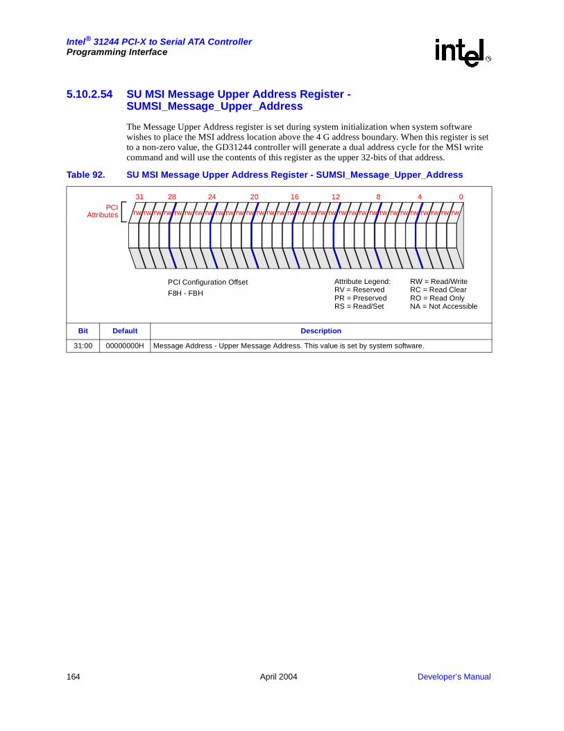
164 April 2004 Developer’s Manual
Intel® 31244 PCI-X to Serial ATA ControllerProgramming Interface
5.10.2.54 SU MSI Message Upper Address Register - SUMSI_Message_Upper_Address
The Message Upper Address register is set during system initialization when system software wishes to place the MSI address location above the 4 G address boundary. When this register is set to a non-zero value, the GD31244 controller will generate a dual address cycle for the MSI write command and will use the contents of this register as the upper 32-bits of that address.
Table 92. SU MSI Message Upper Address Register - SUMSI_Message_Upper_Address
Bit Default Description
31:00 00000000H Message Address - Upper Message Address. This value is set by system software.
PCIAttributes
28 24 20 16 12 8 4 031
rw rw rw rw rw rw rw rw rw rw rw rw rw rw rw rw rw rw rw rw rw rw rw rw rw rw rw rw rw rw rw rw
Attribute Legend:RV = ReservedPR = PreservedRS = Read/Set
RW = Read/WriteRC = Read ClearRO = Read OnlyNA = Not Accessible
PCI Configuration Offset
F8H - FBH
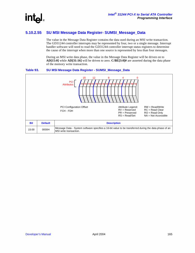
Developer’s Manual April 2004 165
Intel® 31244 PCI-X to Serial ATA ControllerProgramming Interface
5.10.2.55 SU MSI Message Data Register- SUMSI_Message_Data
The value in the Message Data Register contains the data used during an MSI write transaction. The GD31244 controller interrupts may be represented by four, two or a single message. Interrupt handler software will need to read the GD31244 controller interrupt status registers to determine the cause of the interrupt when more than one source is represented by less than four messages.
During an MSI write data phase, the value in the Message Data Register will be driven on to AD[15:0] while AD[31:16] will be driven to zero. C/BE[3:0]# are asserted during the data phase of the memory write transaction.
Table 93. SU MSI Message Data Register - SUMSI_Message_Data
Bit Default Description
15:00 0000H Message Data - System software specifies a 16-bit value to be transferred during the data phase of an MSI write transaction.
PCIAttributes
15 12 8 4 0
rw rw rw rw rw rw rw rw rw rw rw rw rw rw rw rw
Attribute Legend:RV = ReservedPR = PreservedRS = Read/Set
RW = Read/WriteRC = Read ClearRO = Read OnlyNA = Not Accessible
PCI Configuration Offset
FCH - FDH

166 April 2004 Developer’s Manual
Intel® 31244 PCI-X to Serial ATA ControllerProgramming Interface
5.10.3 SU PCI IDE Mode Command Block Registers
This section defines the Command Block Registers when in PCI IDE mode.
5.10.3.1 SU IDE Data Port Register - SUIDR
The SU IDE Data Port Register is a 16-bit read/write register and is used to transfer data during Programmed I/O (PIO) mode reads/writes. On the GD31244 controller, the Data Port register may also be read or written as a 32-bit Data Port. The GD31244 controller internally breaks the 32-bit transaction into two back-to-back 16-bit transactions. It is recommended that the Data Port register is always accessed in either 16-bit or 32-bit quantity for a given PIO sequence. Refer to the AT Attachment with Packet Interface-6 (ATA/ATAPI-6) Specification.
.
Table 94. SU IDE Data Port Register - SUIDR
Bit Default Description
15:00 0000H Data Port - This register is used to transfer data during PIO reads and writes. This register shall be accessed only when the DRQ bit in the status register, SU IDE Status Register - SUISR, is set.
PCIAttributes
15 12 8 4 0
rw rw rw rw rw rw rw rw rw rw rw rw rw rw rw rw
Attribute Legend:RV = ReservedPR = PreservedRS = Read/Set
RW = Read/WriteRC = Read ClearRO = Read OnlyNA = Not Accessible
PCI IDE Mode BAR0/BAR2 Offset
=00H

Developer’s Manual April 2004 167
Intel® 31244 PCI-X to Serial ATA ControllerProgramming Interface
5.10.3.2 SU IDE Error Register - SUIER
The SU IDE Error Register is an 8-bit read-only register. When the SU IDE Error Register is written to, instead the SU IDE Features Register is written. The SU IDE Error Register contains error status for the current command. The content of this register shall be valid when the ERR bit is set in the SU IDE Status Register - SUISR. The SU IDE Error Register is command dependent and the bits are defined in the AT Attachment with Packet Interface-6 (ATA/ATAPI-6) Specification.
Table 95. SU IDE Error Register - SUIER
Bit Default Description
07:00 Device Dependent a
a. After a hardware reset, software reset, or an EXECUTE DEVICE DIAGNOSTIC command, the device will return a diagnostic code. The diagnosticcode is device dependent. AT Attachment with Packet Interface-6 (ATA/ATAPI-6) Specification.
The bits in this register are command dependent. The bits are only valid when the ERR bit (bit 0) in the SU IDE Status Register - SUISR is set. Refer to the AT Attachment with Packet Interface-6 (ATA/ATAPI-6) Specification.
PCIAttributes
7 4 0
ro ro ro ro ro ro ro ro
Attribute Legend:RV = ReservedPR = PreservedRS = Read/Set
RW = Read/WriteRC = Read ClearRO = Read OnlyNA = Not Accessible
PCI IDE Mode BAR0/BAR2 Offset
= 01H

168 April 2004 Developer’s Manual
Intel® 31244 PCI-X to Serial ATA ControllerProgramming Interface
5.10.3.3 SU IDE Features Register - SUIFR
The SU IDE Features Register is a write-only register. When this address is read, instead the SU IDE Error Register is read. The content of the SU IDE Features Register is a command parameter. the content of this register must be loaded before the SU IDE Command Register is written. The content of the SU IDE Features Register is command dependent. Refer to the AT Attachment with Packet Interface-6 (ATA/ATAPI-6) Specification.
Table 96. SU IDE Features Register - SUIFR
Bit Default Description
07:00 00HFeatures - This register is command dependent. For example, it may be a parameter as an extension to the SU IDE Command Register. In the AT Attachment with Packet Interface-6 (ATA/ATAPI-6) Specification, this register acts as a 2-byte FIFO in order to implement a 16-bit Feature register.
PCIAttributes
7 4 0
wowowowo wowo wowo
Attribute Legend:RV = ReservedPR = PreservedRS = Read/Set
WO = Write Only
RW = Read/WriteRC = Read ClearRO = Read OnlyNA = Not Accessible
PCI IDE Mode BAR0/BAR2 Offset
= 01H
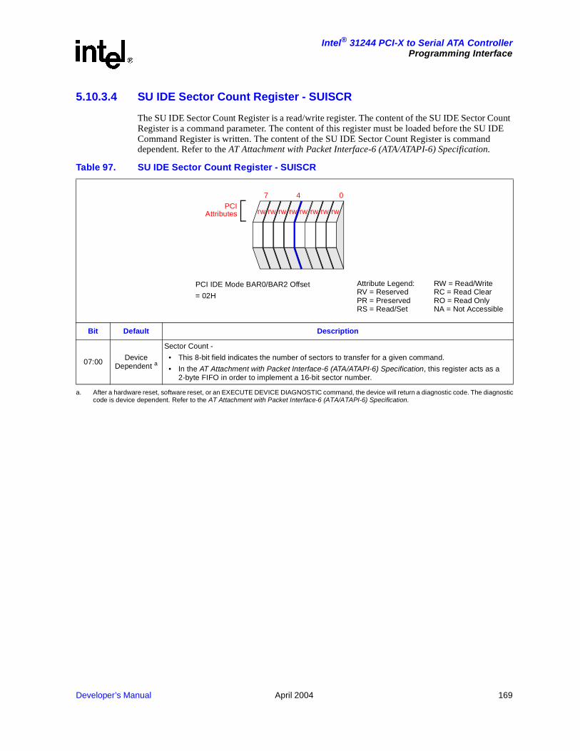
Developer’s Manual April 2004 169
Intel® 31244 PCI-X to Serial ATA ControllerProgramming Interface
5.10.3.4 SU IDE Sector Count Register - SUISCR
The SU IDE Sector Count Register is a read/write register. The content of the SU IDE Sector Count Register is a command parameter. The content of this register must be loaded before the SU IDE Command Register is written. The content of the SU IDE Sector Count Register is command dependent. Refer to the AT Attachment with Packet Interface-6 (ATA/ATAPI-6) Specification.
Table 97. SU IDE Sector Count Register - SUISCR
Bit Default Description
07:00 Device Dependent a
a. After a hardware reset, software reset, or an EXECUTE DEVICE DIAGNOSTIC command, the device will return a diagnostic code. The diagnosticcode is device dependent. Refer to the AT Attachment with Packet Interface-6 (ATA/ATAPI-6) Specification.
Sector Count -
• This 8-bit field indicates the number of sectors to transfer for a given command.
• In the AT Attachment with Packet Interface-6 (ATA/ATAPI-6) Specification, this register acts as a 2-byte FIFO in order to implement a 16-bit sector number.
PCIAttributes
7 4 0
rw rw rw rw rw rw rw rw
Attribute Legend:RV = ReservedPR = PreservedRS = Read/Set
RW = Read/WriteRC = Read ClearRO = Read OnlyNA = Not Accessible
PCI IDE Mode BAR0/BAR2 Offset
= 02H

170 April 2004 Developer’s Manual
Intel® 31244 PCI-X to Serial ATA ControllerProgramming Interface
5.10.3.5 SU IDE Sector Number Register - SUISNR
The SU IDE Sector Number Register is a read/write register. The content of the SU IDE Sector Number Register is a command parameter. The content of this register must be loaded before the SU IDE Command Register is written. The content of this register is command dependent. Refer to the AT Attachment with Packet Interface-6 (ATA/ATAPI-6) Specification.
Table 98. SU IDE Sector Number Register - SUISNR
Bit Default Description
07:00 Device Dependent a
a. After a hardware reset, software reset, or an EXECUTE DEVICE DIAGNOSTIC command, the device will return a diagnostic code. The diagnosticcode is device dependent. Refer to the AT Attachment with Packet Interface-6 (ATA/ATAPI-6) Specification.
Sector Number - This field is dependent on the device access methods. There are three method:
• CHS Mode: This field indicates the sector number.
• 28-bit LBA Mode: This field is used for bit positions LBA[7:0] of the 28-bit addressing LBA[27:0].
• 48-bit LBA Mode: This field is used for bit positions LBA[7:0] and LBA[31:24] of the 48-bit addressing LBA[47:0]. This register acts as a 2-byte FIFO. The higher byte is written first followed by the lower byte.
PCIAttributes
7 4 0
rw rw rw rw rw rw rw rw
Attribute Legend:RV = ReservedPR = PreservedRS = Read/Set
RW = Read/WriteRC = Read ClearRO = Read OnlyNA = Not Accessible
PCI IDE Mode BAR0/BAR2 Offset
= 03H

Developer’s Manual April 2004 171
Intel® 31244 PCI-X to Serial ATA ControllerProgramming Interface
5.10.3.6 SU IDE Cylinder Low Register - SUICLR
The SU IDE Cylinder Low Register is a read/write register. The content of the SU IDE Cylinder Low Register is a command parameter. The content of this register must be loaded before the SU IDE Command Register is written. The content of the SU IDE Cylinder Low Register is command dependent. Refer to the AT Attachment with Packet Interface-6 (ATA/ATAPI-6) Specification.
Table 99. SU IDE Cylinder Low Register - SUICLR
Bit Default Description
07:00 Device Dependent a
a. After a hardware reset, software reset, or an EXECUTE DEVICE DIAGNOSTIC command, the device will return a diagnostic code. The diagnosticcode is device dependent. Refer to the AT Attachment with Packet Interface-6 (ATA/ATAPI-6) Specification.
Cylinder Low - This field is dependent on the device access methods. There are three methods:
• CHS Mode: In CHS mode, this field indicates the lower 8 bits of the 16-bit cylinder number identifier.
• 28-bit LBA Mode: This field is used for bit positions LBA[15:8] of the 28-bit addressing LBA[27:0].
• 48-bit LBA Mode: This field is used for bit positions LBA[15:8] and LBA[39:32] of the 48-bit addressing LBA[47:0]. This register acts as a 2-byte FIFO. The higher byte is written first followed by the lower byte.
PCIAttributes
7 4 0
rw rw rw rw rw rw rw rw
Attribute Legend:RV = ReservedPR = PreservedRS = Read/Set
RW = Read/WriteRC = Read ClearRO = Read OnlyNA = Not Accessible
PCI IDE Mode BAR0/BAR2 Offset
= 04H
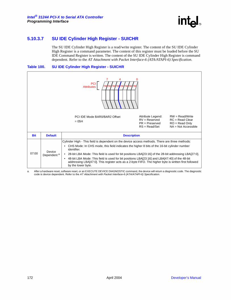
172 April 2004 Developer’s Manual
Intel® 31244 PCI-X to Serial ATA ControllerProgramming Interface
5.10.3.7 SU IDE Cylinder High Register - SUICHR
The SU IDE Cylinder High Register is a read/write register. The content of the SU IDE Cylinder High Register is a command parameter. The content of this register must be loaded before the SU IDE Command Register is written. The content of the SU IDE Cylinder High Register is command dependent. Refer to the AT Attachment with Packet Interface-6 (ATA/ATAPI-6) Specification.
Table 100. SU IDE Cylinder High Register - SUICHR
Bit Default Description
07:00 Device Dependent a
a. After a hardware reset, software reset, or an EXECUTE DEVICE DIAGNOSTIC command, the device will return a diagnostic code. The diagnosticcode is device dependent. Refer to the AT Attachment with Packet Interface-6 (ATA/ATAPI-6) Specification.
Cylinder High - This field is dependent on the device access methods. There are three methods:
• CHS Mode: In CHS mode, this field indicates the higher 8 bits of the 16-bit cylinder number identifier.
• 28-bit LBA Mode: This field is used for bit positions LBA[23:16] of the 28-bit addressing LBA[27:0].
• 48-bit LBA Mode: This field is used for bit positions LBA[23:16] and LBA[47:40] of the 48-bit addressing LBA[47:0]. This register acts as a 2-byte FIFO. The higher byte is written first followed by the lower byte.
PCIAttributes
7 4 0
rw rw rw rw rw rw rw rw
Attribute Legend:RV = ReservedPR = PreservedRS = Read/Set
RW = Read/WriteRC = Read ClearRO = Read OnlyNA = Not Accessible
PCI IDE Mode BAR0/BAR2 Offset
= 05H

Developer’s Manual April 2004 173
Intel® 31244 PCI-X to Serial ATA ControllerProgramming Interface
5.10.3.8 SU IDE Device/Head Register - SUIDR
This SU IDE Device/Head Register is a read/write register. The content of the SU IDE Device/Head Register is a command parameter. The content of this register must be loaded before the SU IDE Command Register is written. The content of the SU IDE Device/Head Register is command dependent. Refer to the AT Attachment with Packet Interface-6 (ATA/ATAPI-6) Specification.
Table 101. SU IDE Device/Head Register - SUIDHR
Bit Default Description
07
Device Dependent a
a. After a hardware reset, software reset, or an EXECUTE DEVICE DIAGNOSTIC command, the device will return a diagnostic code. The diagnosticcode is device dependent. Refer to the AT Attachment with Packet Interface-6 (ATA/ATAPI-6) Specification.
Reserved
06Logical Addressing Mode - This bit indicates the addressing mode:
0 = CHS (Cylinder/Head/Sector) Mode1 = LBA (Logical Block Addressing) Mode
05 Reserved
04Device Select (DEV Bit) - This bit is used to select one of the two devices:
0 = Device 01 = Device 1
03-00
Head - This field is dependent on the device access methods. There are three methods:
• CHS Mode: In CHS mode, this field indicates the head number.
• 28-bit LBA Mode: This field is used for bit positions LBA[27:24] of the 28-bit addressing LBA[27:0].
• 48-bit LBA Mode: This field is reserved.
PCIAttributes
7 4
rv rw rv rw rw rw rw rw
0
Attribute Legend:RV = ReservedPR = PreservedRS = Read/Set
RW = Read/WriteRC = Read ClearRO = Read OnlyNA = Not Accessible
PCI IDE Mode BAR0/BAR2 Offset
= 06H
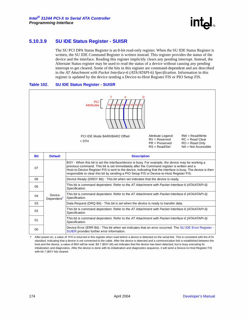
174 April 2004 Developer’s Manual
Intel® 31244 PCI-X to Serial ATA ControllerProgramming Interface
5.10.3.9 SU IDE Status Register - SUISR
The SU PCI DPA Status Register is an 8-bit read-only register. When the SU IDE Status Register is written, the SU IDE Command Register is written instead. This register provides the status of the device and the interface. Reading this register implicitly clears any pending interrupt. Instead, the Alternate Status register may be used to read the status of a device without causing any pending interrupt to get cleared. Some of the bits in this register are command-dependent and are described in the AT Attachment with Packet Interface-6 (ATA/ATAPI-6) Specification. Information in this register is updated by the device sending a Device-to-Host Register FIS or PIO Setup FIS.
Table 102. SU IDE Status Register - SUISR
Bit Default Description
07
Device Dependent†
BSY - When this bit is set the interface/device is busy. For example, the device may be working a previous command. This bit is set immediately after the Command register is written and a Host-to-Device Register FIS is sent to the device, indicating that the interface is busy. The device is then responsible to clear this bit by sending a PIO Setup FIS or Device-to-Host Register FIS.
06 Device Ready (DRDY Bit) - This bit when set indicates that the device is ready.
05 This bit is command dependent. Refer to the AT Attachment with Packet Interface-6 (ATA/ATAPI-6) Specification.
04 This bit is command dependent. Refer to the AT Attachment with Packet Interface-6 (ATA/ATAPI-6) Specification.
03 Data Request (DRQ Bit) - This bit is set when the device is ready to transfer data.
02 This bit is command dependent. Refer to the AT Attachment with Packet Interface-6 (ATA/ATAPI-6) Specification.
01 This bit is command dependent. Refer to the AT Attachment with Packet Interface-6 (ATA/ATAPI-6) Specification.
00 Device Error (ERR Bit) - This bit when set indicates that an error occurred. The SU IDE Error Register - SUIER provides further error information.
† After power-on, a value of 7FH is returned in this register when read before a device is detected on the serial link. This is consistent with the ATA standard, indicating that a device is not connected to the cable. After the device is detected and a communication link is established between the host and the device, a value of 80H will be read. Bit 7 (BSY bit) set indicates that the device has been detected, but is busy executing its initialization and diagnostics. After the device is done with its initialization and diagnostics sequence, it will send a Device-to-Host Register FIS with bit 7 (BSY bit) cleared.
PCIAttributes
7 4 0
ro ro ro ro ro ro ro ro
Attribute Legend:RV = ReservedPR = PreservedRS = Read/Set
RW = Read/WriteRC = Read ClearRO = Read OnlyNA = Not Accessible
PCI IDE Mode BAR0/BAR2 Offset
= 07H

Developer’s Manual April 2004 175
Intel® 31244 PCI-X to Serial ATA ControllerProgramming Interface
5.10.3.10 SU IDE Command Register - SUICR
The SU IDE Command Register is a write-only register. When the SU IDE Command register is read, instead the SU IDE Status register will be read. A command is initiated by writing this register. Refer to the AT Attachment with Packet Interface-6 (ATA/ATAPI-6) Specification.
Table 103. SU IDE Command Register - SUICR
Bit Default Description
07:00 00HCommand - This register is used to initiate a command. This register must be written last. For example, it must be written after the other Command Block registers are written. Because the rest of the registers are parameters for the command.
PCIAttributes
7 4 0
wowowowo wowowo wo
Attribute Legend:RV = ReservedPR = PreservedRS = Read/Set
WO = Write Only
RW = Read/WriteRC = Read ClearRO = Read OnlyNA = Not Accessible
PCI IDE Mode BAR0/BAR2 Offset
= 07H

176 April 2004 Developer’s Manual
Intel® 31244 PCI-X to Serial ATA ControllerProgramming Interface
5.10.4 SU PCI IDE Mode Control Block Registers
This section defines the Device Control and Alternate Status Registers.
5.10.4.1 SU IDE Device Control Register - SUIDCR
The SU IDE Device Control Register is a write-only register. When the SU IDE Device Control Register is read, instead the SU IDE Alternate Status Register is read. The SU IDE Device Control Register is used to initiate a software reset to the device. It is also used to enable/disable interrupt. Refer to the AT Attachment with Packet Interface-6 (ATA/ATAPI-6) Specification.
Table 104. SU IDE Device Control Register - SUIDCR
Bit Default Description
07 02
High Order Byte (HOB Bit) - When operating in 48-bit LBA addressing mode, the Sector Count, Cylinder Low, and Cylinder High registers act a 2-byte deep FIFOs. For example, each of these registers are 16-bit registers with access to only one byte at a time.
The HOB bit provides a mechanism for software to be able to read either byte. Setting this bit to one allows reading the upper byte, while setting the HOB bit to zero allows reading the lower byte
06 02 Reserved.
05 02 Reserved.
04 02 Reserved.
03 02 Reserved.
02 02 SRST - This bit is used by the processor to do a software reset.
01 02nIEN - Interrupt Enable, this bit when cleared enables the assertion of interrupt signal to the processor. When set, interrupt to the processor is masked.
00 02 Reserved. This bit shall always be cleared.
PCIAttributes
7 4 0
wo rv rv rv rv wowo rv
Attribute Legend:RV = ReservedPR = PreservedRS = Read/Set
WO = Write Only
RW = Read/WriteRC = Read ClearRO = Read OnlyNA = Not Accessible
PCI IDE Mode BAR1/BAR3 Offset
= 02H

Developer’s Manual April 2004 177
Intel® 31244 PCI-X to Serial ATA ControllerProgramming Interface
5.10.4.2 SU IDE Alternate Status Register - SUIASR
The SU IDE Alternate Status Register is an 8-bit read-only register. When the SU IDE Alternate Status Register is written to, instead the SU IDE Device Control Register is written. This register contains the same information as the SU IDE Status Register, Table 102, “SU IDE Status Register - SUISR” on page 174. The difference is that when this register is read, any pending interrupt is not cleared. Refer to the AT Attachment with Packet Interface-6 (ATA/ATAPI-6) Specification.
Table 105. SU IDE Alternate Status Register - SUIASR
Bit Default Description
07:00
Refer to Section 102,
“SU IDE Status
Register - SUISR” on page 174.
Alternate Status Register - This register contains the same information as in the SU IDE Status Register. The difference is that when this register is read, any pending interrupts are not cleared. Refer to Section 102, “SU IDE Status Register - SUISR” on page 174.
PCIAttributes
7 4 0
ro ro ro ro ro ro ro ro
Attribute Legend:RV = ReservedPR = PreservedRS = Read/Set
RW = Read/WriteRC = Read ClearRO = Read OnlyNA = Not Accessible
PCI IDE Mode BAR1/BAR3 Offset
= 02H

178 April 2004 Developer’s Manual
Intel® 31244 PCI-X to Serial ATA ControllerProgramming Interface
5.10.5 SU PCI IDE Mode DMA Registers
This section defines the DMA Registers.
5.10.5.1 SU IDE Channel 0 DMA Command Register - SUICDCR0
The SU IDE Channel 0 DMA Command Register enables/disables the DMA engine (bus master capability) and also provides direction control for DMA transfers.
.
Table 106. SU IDE Channel 0 DMA Command Register - SUICDCR0
Bit Default Description
15:10 00H Reserved
09 02
First Party DMA Direction:
0 = From Device to Host1 = From Host to Device
08 02
First Party DMA Active:
0 = Not Active1 = Active
07:04 0H Reserved
03 02
DMA Read/Write Control:
0 = Reads Memory to write FIFO. FIFO data is written to SATA device.1 = Writes Memory with FIFO data. FIFO contains data read from SATA device.
This bit must NOT be changed when the DMA is active. While synchronous DMA transfer is in progress, this bit will be READ ONLY. The bit will return to read/write once the synchronous DMA transfer has been completed or halted.
02:01 002 Reserved.
00 02
Start/Stop DMA Transfer: 1 = Start; 0 = Stop. When this bit is set to 1, the DMA operation starts. The controller transfers data between the device and memory only while this bit is set. Operation may be stopped by writing a 0 to this bit. This results in all state information being lost (i.e., operation cannot be stop and then resumed).
When this bit is set to 0 while bus master operation is still active (i.e., bit 0 = 1 in the DMA Status Register) and data transfer has not yet finished (i.e., bit 2 = 0 in the DMA Status Register), the DMA command is aborted and data transferred from the drive may be discarded by the SATA port rather than being written to memory. This bit is intended to be set to 0 after the data transfer is completed, as indicated by either bit 0 or bit 2 set in the DMA Status Register.
PCIAttributes
15 12 8 4 0
rv rv rv rv rv rv ro ro rv rv rv rv rw rv rv rw
Attribute Legend:RV = ReservedPR = PreservedRS = Read/Set
RW = Read/WriteRC = Read ClearRO = Read OnlyNA = Not Accessible
PCI IDE Mode BAR4 Offset
= 00HPCI IDE Mode BAR4 Offset
= 00H
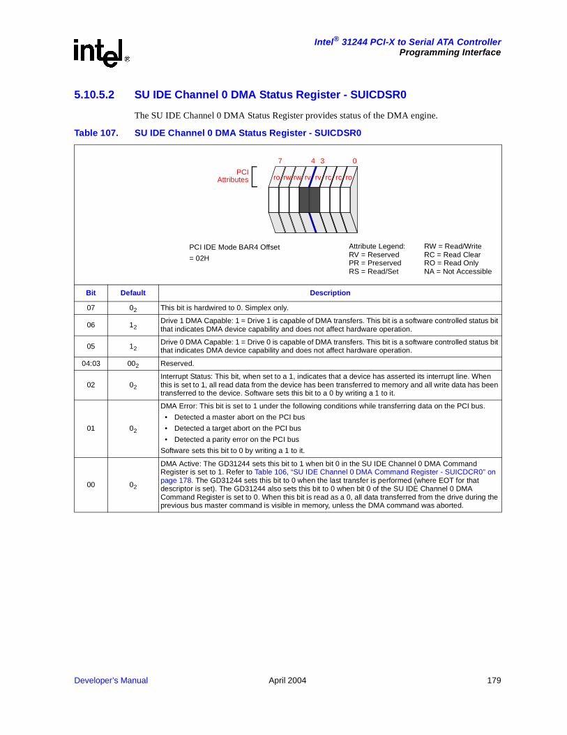
Developer’s Manual April 2004 179
Intel® 31244 PCI-X to Serial ATA ControllerProgramming Interface
5.10.5.2 SU IDE Channel 0 DMA Status Register - SUICDSR0
The SU IDE Channel 0 DMA Status Register provides status of the DMA engine..
Table 107. SU IDE Channel 0 DMA Status Register - SUICDSR0
Bit Default Description
07 02 This bit is hardwired to 0. Simplex only.
06 12Drive 1 DMA Capable: 1 = Drive 1 is capable of DMA transfers. This bit is a software controlled status bit that indicates DMA device capability and does not affect hardware operation.
05 12Drive 0 DMA Capable: 1 = Drive 0 is capable of DMA transfers. This bit is a software controlled status bit that indicates DMA device capability and does not affect hardware operation.
04:03 002 Reserved.
02 02
Interrupt Status: This bit, when set to a 1, indicates that a device has asserted its interrupt line. When this is set to 1, all read data from the device has been transferred to memory and all write data has been transferred to the device. Software sets this bit to a 0 by writing a 1 to it.
01 02
DMA Error: This bit is set to 1 under the following conditions while transferring data on the PCI bus.
• Detected a master abort on the PCI bus
• Detected a target abort on the PCI bus
• Detected a parity error on the PCI bus
Software sets this bit to 0 by writing a 1 to it.
00 02
DMA Active: The GD31244 sets this bit to 1 when bit 0 in the SU IDE Channel 0 DMA Command Register is set to 1. Refer to Table 106, “SU IDE Channel 0 DMA Command Register - SUICDCR0” on page 178. The GD31244 sets this bit to 0 when the last transfer is performed (where EOT for that descriptor is set). The GD31244 also sets this bit to 0 when bit 0 of the SU IDE Channel 0 DMA Command Register is set to 0. When this bit is read as a 0, all data transferred from the drive during the previous bus master command is visible in memory, unless the DMA command was aborted.
PCIAttributes
7 4 0
ro rw rw rv rv rc rc ro
3
Attribute Legend:RV = ReservedPR = PreservedRS = Read/Set
RW = Read/WriteRC = Read ClearRO = Read OnlyNA = Not Accessible
PCI IDE Mode BAR4 Offset
= 02H

180 April 2004 Developer’s Manual
Intel® 31244 PCI-X to Serial ATA ControllerProgramming Interface
5.10.5.3 SU IDE Channel 0 DMA Descriptor Table Pointer Register - SUICDDTPR0
This SU IDE Channel 0 DMA Descriptor Table Pointer Register contains the lower 32-bit PCI address. In PCI IDE mode, the SU IDE Channel 0 DMA Descriptor Table Pointer Register points to system memory.
Table 108. SU IDE Channel 0 DMA Descriptor Table Pointer Register - SUICDDTPR0
Bit Default Description
31:02 0000 0000H PCI Address - is lower PCI address. This register contains the base address of the descriptor table. The descriptor table must be DWORD aligned and must not cross a 64 Kbyte boundary.
01:00 002 Reserved.
PCIAttributes
28 24 20 16 12 8 4 031
rw rw rw rw rw rw rw rw rw rw rw rw rw rw rw rw rw rw rw rw rw rw rw rw rw rw rw rw rw rw rv rv
Attribute Legend:RV = ReservedPR = PreservedRS = Read/Set
RW = Read/WriteRC = Read ClearRO = Read OnlyNA = Not Accessible
PCI IDE Mode BAR4 Offset
= 04H
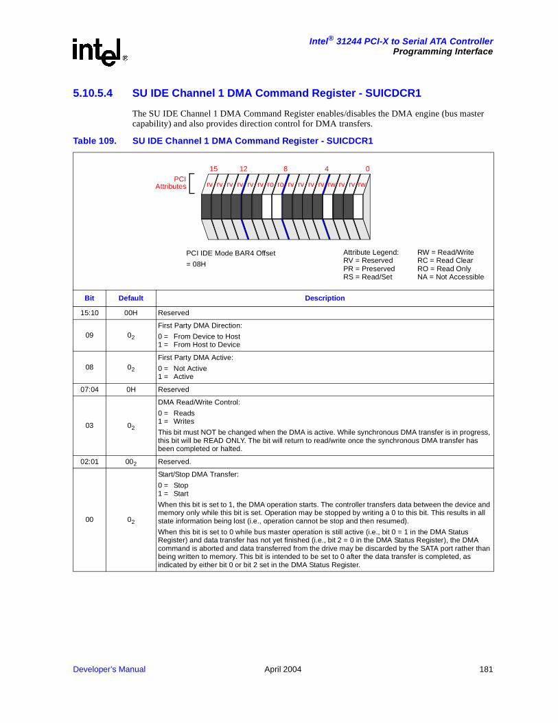
Developer’s Manual April 2004 181
Intel® 31244 PCI-X to Serial ATA ControllerProgramming Interface
5.10.5.4 SU IDE Channel 1 DMA Command Register - SUICDCR1
The SU IDE Channel 1 DMA Command Register enables/disables the DMA engine (bus master capability) and also provides direction control for DMA transfers.
.
Table 109. SU IDE Channel 1 DMA Command Register - SUICDCR1
Bit Default Description
15:10 00H Reserved
09 02
First Party DMA Direction:
0 = From Device to Host1 = From Host to Device
08 02
First Party DMA Active:
0 = Not Active1 = Active
07:04 0H Reserved
03 02
DMA Read/Write Control:
0 = Reads1 = Writes
This bit must NOT be changed when the DMA is active. While synchronous DMA transfer is in progress, this bit will be READ ONLY. The bit will return to read/write once the synchronous DMA transfer has been completed or halted.
02:01 002 Reserved.
00 02
Start/Stop DMA Transfer:
0 = Stop1 = Start
When this bit is set to 1, the DMA operation starts. The controller transfers data between the device and memory only while this bit is set. Operation may be stopped by writing a 0 to this bit. This results in all state information being lost (i.e., operation cannot be stop and then resumed).
When this bit is set to 0 while bus master operation is still active (i.e., bit 0 = 1 in the DMA Status Register) and data transfer has not yet finished (i.e., bit 2 = 0 in the DMA Status Register), the DMA command is aborted and data transferred from the drive may be discarded by the SATA port rather than being written to memory. This bit is intended to be set to 0 after the data transfer is completed, as indicated by either bit 0 or bit 2 set in the DMA Status Register.
PCIAttributes
15 12 8 4 0
rv rv rv rv rv rv ro ro rv rv rv rv rw rv rv rw
Attribute Legend:RV = ReservedPR = PreservedRS = Read/Set
RW = Read/WriteRC = Read ClearRO = Read OnlyNA = Not Accessible
PCI IDE Mode BAR4 Offset
= 08H
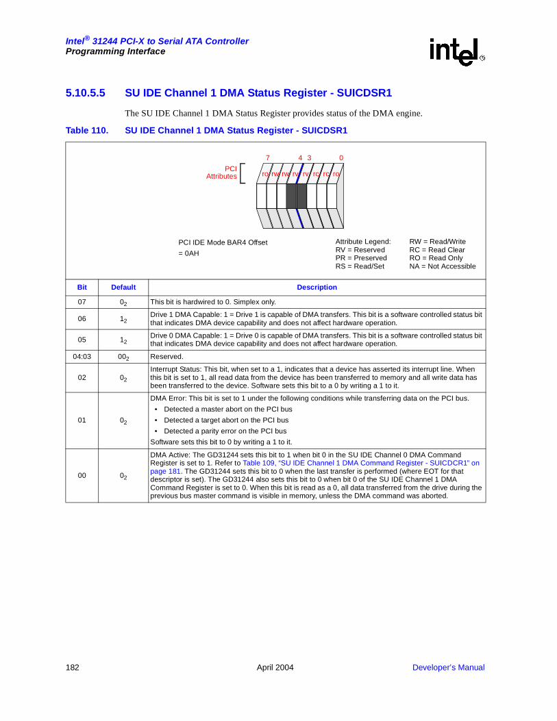
182 April 2004 Developer’s Manual
Intel® 31244 PCI-X to Serial ATA ControllerProgramming Interface
5.10.5.5 SU IDE Channel 1 DMA Status Register - SUICDSR1
The SU IDE Channel 1 DMA Status Register provides status of the DMA engine..
Table 110. SU IDE Channel 1 DMA Status Register - SUICDSR1
Bit Default Description
07 02 This bit is hardwired to 0. Simplex only.
06 12Drive 1 DMA Capable: 1 = Drive 1 is capable of DMA transfers. This bit is a software controlled status bit that indicates DMA device capability and does not affect hardware operation.
05 12Drive 0 DMA Capable: 1 = Drive 0 is capable of DMA transfers. This bit is a software controlled status bit that indicates DMA device capability and does not affect hardware operation.
04:03 002 Reserved.
02 02
Interrupt Status: This bit, when set to a 1, indicates that a device has asserted its interrupt line. When this bit is set to 1, all read data from the device has been transferred to memory and all write data has been transferred to the device. Software sets this bit to a 0 by writing a 1 to it.
01 02
DMA Error: This bit is set to 1 under the following conditions while transferring data on the PCI bus.
• Detected a master abort on the PCI bus
• Detected a target abort on the PCI bus
• Detected a parity error on the PCI bus
Software sets this bit to 0 by writing a 1 to it.
00 02
DMA Active: The GD31244 sets this bit to 1 when bit 0 in the SU IDE Channel 0 DMA Command Register is set to 1. Refer to Table 109, “SU IDE Channel 1 DMA Command Register - SUICDCR1” on page 181. The GD31244 sets this bit to 0 when the last transfer is performed (where EOT for that descriptor is set). The GD31244 also sets this bit to 0 when bit 0 of the SU IDE Channel 1 DMA Command Register is set to 0. When this bit is read as a 0, all data transferred from the drive during the previous bus master command is visible in memory, unless the DMA command was aborted.
PCIAttributes
7 4 03
ro rw rw rv rv rc rc ro
Attribute Legend:RV = ReservedPR = PreservedRS = Read/Set
RW = Read/WriteRC = Read ClearRO = Read OnlyNA = Not Accessible
PCI IDE Mode BAR4 Offset
= 0AH

Developer’s Manual April 2004 183
Intel® 31244 PCI-X to Serial ATA ControllerProgramming Interface
5.10.5.6 SU IDE Channel 1 DMA Descriptor Table Pointer Register - SUICDDTPR1
This SU IDE Channel 1 DMA Descriptor Table Pointer Register contains the lower 32-bit PCI address. In PCI IDE mode, the SU IDE Channel 0 DMA Descriptor Table Pointer Register points to system memory.
Table 111. SU IDE Channel 1 DMA Descriptor Table Pointer Register - SUICDDTPR1
Bit Default Description
31:02 0000 0000H PCI Address - is lower PCI address. This register contains the base address of the descriptor table. The descriptor table must be DWORD aligned and must not cross a 64 Kbyte boundary.
01:00 002 Reserved.
PCIAttributes
28 24 20 16 12 8 4 031
rw rw rw rw rw rw rw rw rw rw rw rw rw rw rw rw rw rw rw rw rw rw rw rw rw rw rw rw rw rw rv rv
Attribute Legend:RV = ReservedPR = PreservedRS = Read/Set
RW = Read/WriteRC = Read ClearRO = Read OnlyNA = Not Accessible
PCI IDE Mode BAR4 Offset
= 0CH

184 April 2004 Developer’s Manual
Intel® 31244 PCI-X to Serial ATA ControllerProgramming Interface
5.10.6 SU PCI DPA Mode Registers
This section defines the SATA Unit registers as viewed from the PCI bus when in Direct Port Access mode. The registers are memory-mapped into the PCI memory space.
Every PCI device/function implements its own separate configuration address space and configuration registers. The PCI Local Bus Specification, Revision 2.2 requires that configuration space be 256 bytes, and the first 64 bytes must adhere to a predefined header format.
Refer to Section 5.10.1, “PCI IDE Mode Registers” on page 103 for the configuration space, as the configuration registers are the same as in the PCI IDE mode. There are a few registers that are different that are highlighted in this section.
When in the Direct Port Access mode, the Serial ATA Unit registers are mapped into the PCI memory space. Only one 64-bit Base Address Register is defined to access all four SATA port registers. Table 112 shows the differences in the configuration space between the two modes.
The SATA Port registers are listed in Table 113. When in Direct Port Access mode, SU PCI DPA Base Address Register 0 - SUDBAR0 and SU PCI DPA Upper Base Address Register 0 - SUPDUBAR0, are used to access the SATA port registers.
Table 112. Configuration Space Comparison
In PCI IDE Mode In Direct Port Access Mode Offset
SU Base Address Register 0 - SUBAR0 SU PCI DPA Base Address Register 0 - SUDBAR0 10H
SU Base Address Register 1 - SUBAR1 SU PCI DPA Upper Base Address Register 0 - SUPDUBAR0 14H
SU Base Address Register 2 - SUBAR2 Reserved 18H
SU Base Address Register 3 - SUBAR3 Reserved 1CH
SU Base Address Register 4 - SUBAR4 Reserved 20H
SU Base Address Register 5 - SUBAR5 Reserved 24H

Developer’s Manual April 2004 185
Intel® 31244 PCI-X to Serial ATA ControllerProgramming Interface
Table 113 shows the SATA port registers. Each SATA port consumes 512 bytes of address space. The Common Port Registers consume 512 bytes. All four SATA ports and the Common Port Registers occupy 4 Kbytes of address space. The SATA port registers are defined in Section 5.10.8, “SU PCI DPA Mode Common SATA Port Registers” on page 194 through Section 5.10.12, “SU PCI DPA Mode Superset Registers” on page 220.
Table 113. SATA Port Registers Mapping in PCI DPA Mode (Sheet 1 of 7)
Register Name Offset
SU PCI DPA Interrupt Pending Register - SUPDIPR 000H
SU PCI DPA Interrupt Mask Register - SUPDIMR 004H
Reserved. 008H - 1FFH
SU PCI DPA Data Port Register - SUPDDR
Port 0 - 200H
Port 1 - 400H
Port 2 - 600H
Port 3 - 800H
SU PCI DPA Error Register - SUPDER
Port 0 - 204H
Port 1 - 404H
Port 2 - 604H
Port 3 - 804H
SU PCI DPA Features Register - SUPDFR
Port 0 - 206H
Port 1 - 406H
Port 2 - 606H
Port 3 - 806H
SU PCI DPA Sector Count Register - SUPDSCR
Port 0 - 208H
Port 1 - 408H
Port 2 - 608H
Port 3 - 808H
SU PCI DPA Sector Number Register - SUPDSNR
Port 0 - 20CH
Port 1 - 40CH
Port 2 - 60CH
Port 3 - 80CH
SU PCI DPA Cylinder Low Register - SUPDCLR
Port 0 - 210H
Port 1 - 410H
Port 2 - 610H
Port 3 - 810H
SU PCI DPA Cylinder High Register - SUPDCHR
Port 0 - 214H
Port 1 - 414H
Port 2 - 614H
Port 3 - 814H
SU PCI DPA Device/Head Register - SUPDDHR
Port 0 - 218H
Port 1 - 418H
Port 2 - 618H
Port 3 - 818H
SU PCI DPA Status Register - SUPDSR
Port 0 - 21CH
Port 1 - 41CH
Port 2 - 61CH
Port 3 - 81CH

186 April 2004 Developer’s Manual
Intel® 31244 PCI-X to Serial ATA ControllerProgramming Interface
SU PCI DPA Command Register - SUPDCR
Port 0 - 21DH
Port 1 - 41DH
Port 2 - 61DH
Port 3 - 81DH
Reserved.
Port 0 - 220H - 227H
Port 1 - 420H - 427H
Port 2 - 620H - 627H
Port 3 - 820H - 827H
SU PCI DPA Alternate Status Register - SUPDASR
Port 0 - 228H
Port 1 - 428H
Port 2 - 628H
Port 3 - 828H
SU PCI DPA Device Control Register - SUPDDCTLR
Port 0 - 229H
Port 1 - 429H
Port 2 - 629H
Port 3 - 829H
Reserved.
Port 0 - 22CH - 25FH
Port 1 - 42CH - 42FH
Port 2 - 62CH - 62FH
Port 3 - 82CH - 82FH
Reserved.
Port 0 - 260H
Port 1 - 460H
Port 2 - 660H
Port 3 - 860H
SU PCI DPA Upper DMA Descriptor Table Pointer Register - SUPDUDDTPR
Port 0 - 264H
Port 1 - 464H
Port 2 - 664H
Port 3 - 864H
Reserved.
Port 0 - 268H
Port 1 - 468H
Port 2 - 668H
Port 3 - 868H
SU PCI DPA Upper DMA Data Buffer Pointer Register - SUPDUDDPR.
Port 0 - 26CH
Port 1 - 46CH
Port 2 - 66CH
Port 3 - 86CH
SU PCI DPA DMA Command Register - SUPDDCMDR
Port 0 - 270H
Port 1 - 470H
Port 2 - 670H
Port 3 - 870H
SU PCI DPA DMA Status Register - SUPDDSR
Port 0 - 272H
Port 1 - 472H
Port 2 - 672H
Port 3 - 872H
Table 113. SATA Port Registers Mapping in PCI DPA Mode (Sheet 2 of 7)
Register Name Offset

Developer’s Manual April 2004 187
Intel® 31244 PCI-X to Serial ATA ControllerProgramming Interface
SU PCI DPA DMA Descriptor Table Pointer Register - SUPDDDTPR
Port 0 - 274H
Port 1 - 474H
Port 2 - 674H
Port 3 - 874H
Reserved.
Port 0 - 278H - 2FFH
Port 1 - 478H - 4FFH
Port 2 - 678H - 6FFH
Port 3 - 878H - 8FFH
SU PCI DPA SATA SStatus Register - SUPDSSSR
Port 0 - 300H
Port 1 - 500H
Port 2 - 700H
Port 3 - 900H
SU PCI DPA SATA SError Register - SUPDSSER
Port 0 - 304H
Port 1 - 504H
Port 2 - 704H
Port 3 - 904H
SU PCI DPA SATA SControl Register - SUPDSSCR
Port 0 - 308H
Port 1 - 508H
Port 2 - 708H
Port 3 - 908H
SU PCI DPA Set Device Bits Register - SUPDSDBR
Port 0 - 30CH
Port 1 - 50CH
Port 2 - 70CH
Port 3 - 90CH
Reserved.
Port 0 - 310H - 33FH
Port 1 - 510H - 53FH
Port 2 - 710H - 73FH
Port 3 - 910H - 93FH
SU PCI DPA PHY Feature Register - SUPDPFR
Port 0 - 340H
Port 1 - 540H
Port 2 - 740H
Port 3 - 940H
SU PCI DPA BIST FIS Control and Status Register - SUPDBFCSR
Port 0 - 344H
Port 1 - 544H
Port 2 - 744H
Port 3 - 944H
SU PCI DPA BIST Errors Register - SUPDBER
Port 0 - 348H
Port 1 - 548H
Port 2 - 748H
Port 3 - 948H
SU PCI DPA BIST Frames Register - SUPDBFR
Port 0 - 34CH
Port 1 - 54CH
Port 2 - 74CH
Port 3 - 94CH
Table 113. SATA Port Registers Mapping in PCI DPA Mode (Sheet 3 of 7)
Register Name Offset
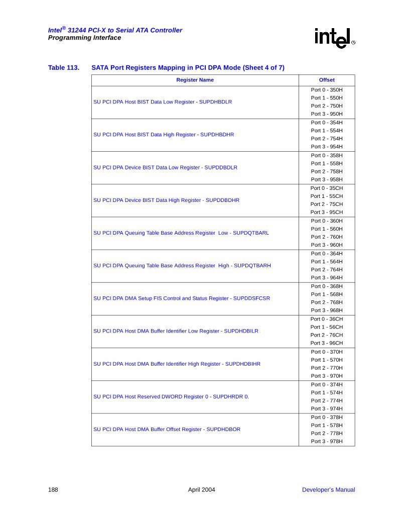
188 April 2004 Developer’s Manual
Intel® 31244 PCI-X to Serial ATA ControllerProgramming Interface
SU PCI DPA Host BIST Data Low Register - SUPDHBDLR
Port 0 - 350H
Port 1 - 550H
Port 2 - 750H
Port 3 - 950H
SU PCI DPA Host BIST Data High Register - SUPDHBDHR
Port 0 - 354H
Port 1 - 554H
Port 2 - 754H
Port 3 - 954H
SU PCI DPA Device BIST Data Low Register - SUPDDBDLR
Port 0 - 358H
Port 1 - 558H
Port 2 - 758H
Port 3 - 958H
SU PCI DPA Device BIST Data High Register - SUPDDBDHR
Port 0 - 35CH
Port 1 - 55CH
Port 2 - 75CH
Port 3 - 95CH
SU PCI DPA Queuing Table Base Address Register Low - SUPDQTBARL
Port 0 - 360H
Port 1 - 560H
Port 2 - 760H
Port 3 - 960H
SU PCI DPA Queuing Table Base Address Register High - SUPDQTBARH
Port 0 - 364H
Port 1 - 564H
Port 2 - 764H
Port 3 - 964H
SU PCI DPA DMA Setup FIS Control and Status Register - SUPDDSFCSR
Port 0 - 368H
Port 1 - 568H
Port 2 - 768H
Port 3 - 968H
SU PCI DPA Host DMA Buffer Identifier Low Register - SUPDHDBILR
Port 0 - 36CH
Port 1 - 56CH
Port 2 - 76CH
Port 3 - 96CH
SU PCI DPA Host DMA Buffer Identifier High Register - SUPDHDBIHR
Port 0 - 370H
Port 1 - 570H
Port 2 - 770H
Port 3 - 970H
SU PCI DPA Host Reserved DWORD Register 0 - SUPDHRDR 0.
Port 0 - 374H
Port 1 - 574H
Port 2 - 774H
Port 3 - 974H
SU PCI DPA Host DMA Buffer Offset Register - SUPDHDBOR
Port 0 - 378H
Port 1 - 578H
Port 2 - 778H
Port 3 - 978H
Table 113. SATA Port Registers Mapping in PCI DPA Mode (Sheet 4 of 7)
Register Name Offset

Developer’s Manual April 2004 189
Intel® 31244 PCI-X to Serial ATA ControllerProgramming Interface
SU PCI DPA Host DMA Transfer Count Register - SUPDHDTCR
Port 0 - 37CH
Port 1 - 57CH
Port 2 - 77CH
Port 3 - 87CH
SU PCI DPA Host Reserved DWORD Register 1- SUPDHRDR 1.
Port 0 - 380H
Port 1 - 580H
Port 2 - 780H
Port 3 - 980H
SU PCI DPA Device DMA Buffer Identifier Low Register - SUPDDDBILR
Port 0 - 384H
Port 1 - 584H
Port 2 - 784H
Port 3 - 984H
SU PCI DPA Device DMA Buffer Identifier High Register - SUPDDDBIHR
Port 0 - 388H
Port 1 - 588H
Port 2 - 788H
Port 3 - 988H
SU PCI DPA Device Reserved DWORD Register 0 - SUPDDRDR0
Port 0 - 38CH
Port 1 - 58CH
Port 2 - 78CH
Port 3 - 98CH
SU PCI DPA Device DMA Buffer Offset Register - SUPDDDBOR
Port 0 - 390H
Port 1 - 590H
Port 2 - 790H
Port 3 - 990H
SU PCI DPA Device DMA Transfer Count Register - SUPDDTCR
Port 0 - 394H
Port 1 - 594H
Port 2 - 794H
Port 3 - 994H
Reserved Word
Port 0 - 398H
Port 1 - 598H
Port 2 - 798H
Port 3 - 998H
Reserved Word
Port 0 - 39CH
Port 1 - 59CH
Port 2 - 79CH
Port 3 - 99CH
Reserved Word
Port 0 - 3A0H
Port 1 - 5A0H
Port 2 - 7A0H
Port 3 - 9A0H
Reserved Word
Port 0 - 3A4H
Port 1 - 5A4H
Port 2 - 7A4H
Port 3 - 9A4H
Table 113. SATA Port Registers Mapping in PCI DPA Mode (Sheet 5 of 7)
Register Name Offset

190 April 2004 Developer’s Manual
Intel® 31244 PCI-X to Serial ATA ControllerProgramming Interface
Reserved Word
Port 0 - 3A8H
Port 1 - 5A8H
Port 2 - 7A8H
Port 3 - 9A8H
Reserved Word
Port 0 - 3ACH
Port 1 - 5ACH
Port 2 - 7ACH
Port 3 - 9ACH
Reserved Word
Port 0 - 3B0H
Port 1 - 5B0H
Port 2 - 7B0H
Port 3 - 9B0H
Reserved Word
Port 0 - 3B4H
Port 1 - 5B4H
Port 2 - 7B4H
Port 3 - 9B4H
Reserved Word
Port 0 - 3B8H
Port 1 - 5B8H
Port 2 - 7B8H
Port 3 - 9B8H
Reserved Word
Port 0 - 3BCH
Port 1 - 5BCH
Port 2 - 7BCH
Port 3 - 9BCH
Reserved Word
Port 0 - 3C0H
Port 1 - 5C0H
Port 2 - 7C0H
Port 3 - 9C0H
Reserved Word
Port 0 - 3C4H
Port 1 - 5C4H
Port 2 - 7C4H
Port 3 - 9C4H
Reserved Word
Port 0 - 3C8H
Port 1 - 5C8H
Port 2 - 7C8H
Port 3 - 9C8H
Test Register 0
Port 0 - 3CCH
Port 1 - 5CCH
Port 2 - 7CCH
Port 3 - 9CCH
Table 113. SATA Port Registers Mapping in PCI DPA Mode (Sheet 6 of 7)
Register Name Offset
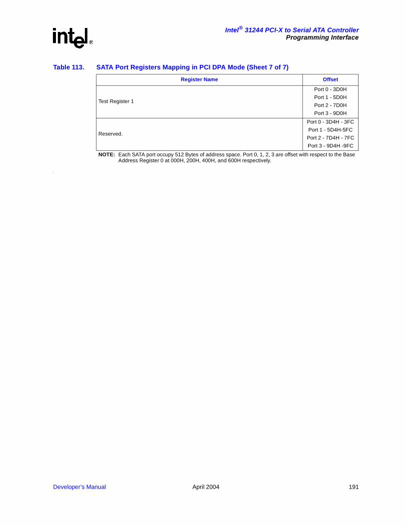
Developer’s Manual April 2004 191
Intel® 31244 PCI-X to Serial ATA ControllerProgramming Interface
s
Test Register 1
Port 0 - 3D0H
Port 1 - 5D0H
Port 2 - 7D0H
Port 3 - 9D0H
Reserved.
Port 0 - 3D4H - 3FC
Port 1 - 5D4H-5FC
Port 2 - 7D4H - 7FC
Port 3 - 9D4H -9FC
NOTE: Each SATA port occupy 512 Bytes of address space. Port 0, 1, 2, 3 are offset with respect to the Base Address Register 0 at 000H, 200H, 400H, and 600H respectively.
Table 113. SATA Port Registers Mapping in PCI DPA Mode (Sheet 7 of 7)
Register Name Offset

192 April 2004 Developer’s Manual
Intel® 31244 PCI-X to Serial ATA ControllerProgramming Interface
5.10.7 SU PCI DPA Mode Base Address Registers
This section defines the configuration registers that are different in PCI Direct Port Access mode.
5.10.7.1 SU PCI DPA Base Address Register 0 - SUPDBAR0
The SU PCI DPA Base Address Register 0 (SUDBAR0) together with the SU PCI DPA Upper Base Address Register 0 (SUDUBAR0) defines the block of memory addresses in which the SATA Ports registers are mapped.
Table 114. SU PCI DPA Base Address Register 0 - SUDBAR0
Bit Default Description
31:12 00000H Base Address 0 - These bits define the actual location the SATA Unit is to respond to when addressed from the PCI bus.
11:04 00H Reserved.
03 02 Prefetchable Indicator - When cleared, defines the memory space as non-prefetchable.
02:01 102
Type Indicator - Defines the width of the addressability for this memory window:
00 - Memory Window is locatable anywhere in 32 bit address space.10 - Memory Window is locatable anywhere in 64 bit address space.
00 02Memory Space Indicator - This bit field describes memory or I/O space base address. The SATA Unit in Direct Port Access mode is mapped in Memory space, thus this bit must be zero.
PCIAttributes
28 24 20 16 12 8 4 031
rw rw rw rw rw rw rw rw rw rw rw rw rw rw rw rw rw rw rw rw rv rv rv rv rv rv rv rv ro ro ro ro
Attribute Legend:RV = ReservedPR = PreservedRS = Read/Set
RW = Read/WriteRC = Read ClearRO = Read OnlyNA = Not Accessible
PCI Configuration Address Offset
10H -13H
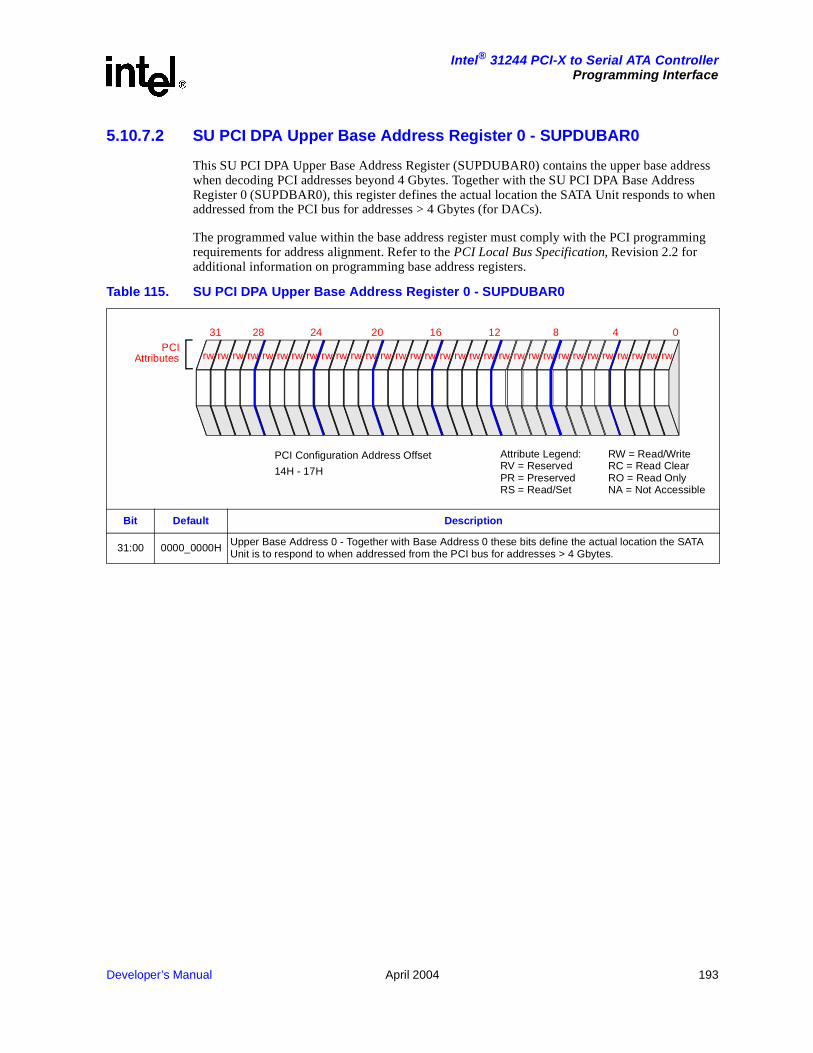
Developer’s Manual April 2004 193
Intel® 31244 PCI-X to Serial ATA ControllerProgramming Interface
5.10.7.2 SU PCI DPA Upper Base Address Register 0 - SUPDUBAR0
This SU PCI DPA Upper Base Address Register (SUPDUBAR0) contains the upper base address when decoding PCI addresses beyond 4 Gbytes. Together with the SU PCI DPA Base Address Register 0 (SUPDBAR0), this register defines the actual location the SATA Unit responds to when addressed from the PCI bus for addresses > 4 Gbytes (for DACs).
The programmed value within the base address register must comply with the PCI programming requirements for address alignment. Refer to the PCI Local Bus Specification, Revision 2.2 for additional information on programming base address registers.
Table 115. SU PCI DPA Upper Base Address Register 0 - SUPDUBAR0
Bit Default Description
31:00 0000_0000H Upper Base Address 0 - Together with Base Address 0 these bits define the actual location the SATA Unit is to respond to when addressed from the PCI bus for addresses > 4 Gbytes.
PCIAttributes
28 24 20 16 12 8 4 031
rw rw rw rw rw rw rw rw rw rw rw rw rw rw rw rw rw rw rw rw rw rw rw rw rw rw rw rw rw rw rw rw
Attribute Legend:RV = ReservedPR = PreservedRS = Read/Set
RW = Read/WriteRC = Read ClearRO = Read OnlyNA = Not Accessible
PCI Configuration Address Offset
14H - 17H

194 April 2004 Developer’s Manual
Intel® 31244 PCI-X to Serial ATA ControllerProgramming Interface
5.10.8 SU PCI DPA Mode Common SATA Port Registers
This section defines registers that are common to all the four SATA Ports.
5.10.8.1 SU PCI DPA Interrupt Pending Register - SUPDIPR
The SU PCI DPA Interrupt Pending Register is a 32-bit read-only register. This register is used to report interrupts generated by the SATA ports. Software must clear any pending interrupt at the appropriate sources. The IDE interrupts (bits 31, 23, 15, 7) are cleared by reading the SATA Port Command Block Status register. Other pending interrupts in this register are generated by the SError registers, and must be cleared by writing 1s to the SError registers.
Table 116. SU PCI DPA Interrupt Pending Register - SUPDIPR (Sheet 1 of 5)
Bit Default Description
31 02
SATA Port 3 IDE Interrupt - When set, this bit indicates that the SATA device generated an interrupt. This is the same as PCI IDE compatible interrupt. The source of this interrupt is based on the setting of the ‘I’ bit in the Device-to-Host Register FIS. This interrupt is cleared by reading the taskfile Status register.
30 02
SATA Port 3 CRC Error Detect Interrupt - When set, this bit indicates that a CRC error was detected on a previous data transfer. The source of this interrupt is from bit 21 (DIAG_C) of the SError register. This interrupt is cleared by writing a 1 to bit 21 of the SError register. Refer to Section 5.10.12.2, “SU PCI DPA SATA SError Register - SUPDSSER” on page 222.
29 02
SATA Port 3 Data Integrity Interrupt - When set, this bit indicates that a CRC, disparity error was detected by the host, or an R_ERR primitive was returned by the device in response to a Data FIS transfer. The source of this interrupt is from bit 8 (ERR_T) of the SError register. This interrupt is cleared by writing a 1 to bit 8 of the SError register. Refer to Section 5.10.12.2, “SU PCI DPA SATA SError Register - SUPDSSER” on page 222.
28 02
SATA Port 3 Unrecognized FIS Reception Interrupt - When set, this bit indicates that an unsupported FIS was detected. The source of this interrupt is from bit 10 (ERR_P) of the SError register. This interrupt is cleared by writing a 1 to bit 10 of the SError register. Refer to Section 5.10.12.2, “SU PCI DPA SATA SError Register - SUPDSSER” on page 222.
27 02
SATA Port 3 R_ERR Primitive Received Interrupt - When set, this bit indicates that an R_ERR primitive was received during a Data FIS transfer. The source of this interrupt is from bit 22 (DIAG_H) of the SError register. This interrupt is cleared by writing a 1 to bit 22 of the SError register. Refer to Section 5.10.12.2, “SU PCI DPA SATA SError Register - SUPDSSER” on page 222.
26 02
SATA Port 3 FIFO Error Interrupt - When set, a FIFO error occurred during a Data FIS transfer. The source of this interrupt is from bit 11 (ERR_E) of the SError register. This interrupt is cleared by writing a 1 to bit 11 of the SError register. Refer to Section 5.10.12.2, “SU PCI DPA SATA SError Register - SUPDSSER” on page 222.
PCIAttributes
28 24 20 16 12 8 4 031
ro ro ro ro ro ro ro ro ro ro ro ro ro ro ro ro ro ro ro ro ro ro ro ro ro ro ro ro ro ro ro ro
Attribute Legend:RV = ReservedPR = PreservedRS = Read/Set
RW = Read/WriteRC = Read ClearRO = Read OnlyNA = Not Accessible
DPA Mode BAR0 Offset
000H

Developer’s Manual April 2004 195
Intel® 31244 PCI-X to Serial ATA ControllerProgramming Interface
25 02
SATA Port 3 PHY Ready Interrupt - When set, a SATA Port 0 PHY became READY from NOT READY. OOB is done. The source of this interrupt is from bit 1 (ERR_M) of the SError register. This interrupt is cleared by writing a 1 to bit 1 of the SError register. Refer to Section 5.10.12.2, “SU PCI DPA SATA SError Register - SUPDSSER” on page 222.
The default value after reset is 02, for example the PHY will not be ready. When the PHY becomes ready as part of the initialization sequence, the value will change to 12.
24 02
SATA Port 3 PHY Change State Interrupt - When set, the PHY either went from READY to NOT-READY, or from NOT-READY to READY. The source of this interrupt is from bit 16 (DIAG_N) of the SError register. This interrupt is cleared by writing a 1 to bit 16 of the SError register. Refer to Section 5.10.12.2, “SU PCI DPA SATA SError Register - SUPDSSER” on page 222.
The default value after reset is 02, for example the PHY will not be ready. When the PHY becomes ready (state change from not-ready to ready) as part of the initialization sequence, the value will change to 12.
23 02
SATA Port 2 IDE Interrupt - When set, this bit indicates that the SATA device generated an interrupt. This is the same as PCI IDE compatible interrupt. The source of this interrupt is based on the setting of the “I” bit in the Device-to-Host Register FIS. This interrupt is cleared by reading the taskfile Status register.
22 02
SATA Port 2 CRC Error Detect Interrupt - When set, this bit indicates that a CRC error was detected on a previous data transfer. The source of this interrupt is from bit 21 (DIAG_C) of the SError register. This interrupt is cleared by writing a 1 to bit 21 of the SError register. Refer to Section 5.10.12.2, “SU PCI DPA SATA SError Register - SUPDSSER” on page 222.
21 02
SATA Port 2 Data Integrity Interrupt - When set, this bit indicates that a CRC, disparity error was detected by the host, or an R_ERR was returned by the device in response to a Data FIS transfer. The source of this interrupt is from bit 8 (ERR_T) of the SError register. This interrupt is cleared by writing a 1 to bit 8 of the SError register. Refer to Section 5.10.12.2, “SU PCI DPA SATA SError Register - SUPDSSER” on page 222.
20 02
SATA Port 2 Unrecognized FIS Reception Interrupt - When set, this bit indicates that an unsupported FIS was detected. The source of this interrupt is from bit 10 (ERR_P) of the SError register. This interrupt is cleared by writing a 1 to bit 10 of the SError register. Refer to Section 5.10.12.2, “SU PCI DPA SATA SError Register - SUPDSSER” on page 222.
19 02
SATA Port 2 R_ERR Primitive Received Interrupt - When set, this bit indicates that an R_ERR primitive was received during a Data FIS transfer. The source of this interrupt is from bit 22 (DIAG_H) of the SError register. This interrupt is cleared by writing a 1 to bit 22 of the SError register. Refer to Section 5.10.12.2, “SU PCI DPA SATA SError Register - SUPDSSER” on page 222.
18 02
SATA Port 2 FIFO Error Interrupt - When set, a FIFO error occurred during a Data FIS transfer. The source of this interrupt is from bit 11 (ERR_E) of the SError register. This interrupt is cleared by writing a 1 to bit 11 of the SError register. Refer to Section 5.10.12.2, “SU PCI DPA SATA SError Register - SUPDSSER” on page 222.
17 02
SATA Port 2 PHY Ready Interrupt - When set, a SATA Port 0 PHY became READY from NOT READY. OOB is done. The source of this interrupt is from bit 1 (ERR_M) of the SError register. This interrupt is cleared by writing a 1 to bit 1 of the SError register. Refer to Section 5.10.12.2, “SU PCI DPA SATA SError Register - SUPDSSER” on page 222.
The default value after reset is 02, for example the PHY will not be ready. When the PHY becomes ready as part of the initialization sequence, the value will change to 12.
Table 116. SU PCI DPA Interrupt Pending Register - SUPDIPR (Sheet 2 of 5)
Bit Default Description
PCIAttributes
28 24 20 16 12 8 4 031
ro ro ro ro ro ro ro ro ro ro ro ro ro ro ro ro ro ro ro ro ro ro ro ro ro ro ro ro ro ro ro ro
Attribute Legend:RV = ReservedPR = PreservedRS = Read/Set
RW = Read/WriteRC = Read ClearRO = Read OnlyNA = Not Accessible
DPA Mode BAR0 Offset
000H

196 April 2004 Developer’s Manual
Intel® 31244 PCI-X to Serial ATA ControllerProgramming Interface
25 02
SATA Port 3 PHY Ready Interrupt - When set, a SATA Port 0 PHY became READY from NOT READY. OOB is done. The source of this interrupt is from bit 1 (ERR_M) of the SError register. This interrupt is cleared by writing a 1 to bit 1 of the SError register. Refer to Section 5.10.12.2, “SU PCI DPA SATA SError Register - SUPDSSER” on page 222.
The default value after reset is 02, for example the PHY will not be ready. When the PHY becomes ready as part of the initialization sequence, the value will change to 12.
24 02
SATA Port 3 PHY Change State Interrupt - When set, the PHY either went from READY to NOT-READY, or from NOT-READY to READY. The source of this interrupt is from bit 16 (DIAG_N) of the SError register. This interrupt is cleared by writing a 1 to bit 16 of the SError register. Refer to Section 5.10.12.2, “SU PCI DPA SATA SError Register - SUPDSSER” on page 222.
The default value after reset is 02, for example the PHY will not be ready. When the PHY becomes ready (state change from not-ready to ready) as part of the initialization sequence, the value will change to 12.
23 02
SATA Port 2 IDE Interrupt - When set, this bit indicates that the SATA device generated an interrupt. This is the same as PCI IDE compatible interrupt. The source of this interrupt is based on the setting of the “I” bit in the Device-to-Host Register FIS. This interrupt is cleared by reading the taskfile Status register.
22 02
SATA Port 2 CRC Error Detect Interrupt - When set, this bit indicates that a CRC error was detected on a previous data transfer. The source of this interrupt is from bit 21 (DIAG_C) of the SError register. This interrupt is cleared by writing a 1 to bit 21 of the SError register. Refer to Section 5.10.12.2, “SU PCI DPA SATA SError Register - SUPDSSER” on page 222.
21 02
SATA Port 2 Data Integrity Interrupt - When set, this bit indicates that a CRC, disparity error was detected by the host, or an R_ERR was returned by the device in response to a Data FIS transfer. The source of this interrupt is from bit 8 (ERR_T) of the SError register. This interrupt is cleared by writing a 1 to bit 8 of the SError register. Refer to Section 5.10.12.2, “SU PCI DPA SATA SError Register - SUPDSSER” on page 222.
20 02
SATA Port 2 Unrecognized FIS Reception Interrupt - When set, this bit indicates that an unsupported FIS was detected. The source of this interrupt is from bit 10 (ERR_P) of the SError register. This interrupt is cleared by writing a 1 to bit 10 of the SError register. Refer to Section 5.10.12.2, “SU PCI DPA SATA SError Register - SUPDSSER” on page 222.
19 02
SATA Port 2 R_ERR Primitive Received Interrupt - When set, this bit indicates that an R_ERR primitive was received during a Data FIS transfer. The source of this interrupt is from bit 22 (DIAG_H) of the SError register. This interrupt is cleared by writing a 1 to bit 22 of the SError register. Refer to Section 5.10.12.2, “SU PCI DPA SATA SError Register - SUPDSSER” on page 222.
18 02
SATA Port 2 FIFO Error Interrupt - When set, a FIFO error occurred during a Data FIS transfer. The source of this interrupt is from bit 11 (ERR_E) of the SError register. This interrupt is cleared by writing a 1 to bit 11 of the SError register. Refer to Section 5.10.12.2, “SU PCI DPA SATA SError Register - SUPDSSER” on page 222.
17 02
SATA Port 2 PHY Ready Interrupt - When set, a SATA Port 0 PHY became READY from NOT READY. OOB is done. The source of this interrupt is from bit 1 (ERR_M) of the SError register. This interrupt is cleared by writing a 1 to bit 1 of the SError register. Refer to Section 5.10.12.2, “SU PCI DPA SATA SError Register - SUPDSSER” on page 222.
The default value after reset is 02, for example the PHY will not be ready. When the PHY becomes ready as part of the initialization sequence, the value will change to 12.
Table 116. SU PCI DPA Interrupt Pending Register - SUPDIPR (Sheet 2 of 5)
Bit Default Description
PCIAttributes
28 24 20 16 12 8 4 031
ro ro ro ro ro ro ro ro ro ro ro ro ro ro ro ro ro ro ro ro ro ro ro ro ro ro ro ro ro ro ro ro
Attribute Legend:RV = ReservedPR = PreservedRS = Read/Set
RW = Read/WriteRC = Read ClearRO = Read OnlyNA = Not Accessible
DPA Mode BAR0 Offset
000H

Developer’s Manual April 2004 197
Intel® 31244 PCI-X to Serial ATA ControllerProgramming Interface
16 02
SATA Port 2 PHY Change State Interrupt - When set, the PHY either went from READY to NOT-READY, or from NOT-READY to READY. The source of this interrupt is from bit 16 (DIAG_N) of the SError register. This interrupt is cleared by writing a 1 to bit 16 of the SError register. Refer to Section 5.10.12.2, “SU PCI DPA SATA SError Register - SUPDSSER” on page 222.
The default value after reset is 02, for example the PHY will not be ready. When the PHY becomes ready (state change from not-ready to ready) as part of the initialization sequence, the value will change to 12.
15 02
SATA Port 1 IDE Interrupt - When set, this bit indicates that the SATA device generated an interrupt. This is the same as PCI IDE compatible interrupt. The source of this interrupt is based on the setting of the “I” bit in the Device-to-Host Register FIS. This interrupt is cleared by reading the taskfile Status register.
14 02
SATA Port 1 CRC Error Detect Interrupt - When set, this bit indicates that a CRC error was detected on a previous data transfer. The source of this interrupt is from bit 21 (DIAG_C) of the SError register. This interrupt is cleared by writing a 1 to bit 21 of the SError register. Refer to Section 5.10.12.2, “SU PCI DPA SATA SError Register - SUPDSSER” on page 222.
13 02
SATA Port 1 Data Integrity Interrupt - When set, this bit indicates that a CRC, disparity error was detected by the host, or an R_ERR primitive was returned by the device in response to a Data FIS transfer. The source of this interrupt is from bit 8 (ERR_T) of the SError register. This interrupt is cleared by writing a 1 to bit 8 of the SError register. Refer to Section 5.10.12.2, “SU PCI DPA SATA SError Register - SUPDSSER” on page 222.
12 02
SATA Port 1 Unrecognized FIS Reception Interrupt - When set, this bit indicates that an unsupported FIS was detected. The source of this interrupt is from bit 10 (ERR_P) of the SError register. This interrupt is cleared by writing a 1 to bit 10 of the SError register. Refer to Section 5.10.12.2, “SU PCI DPA SATA SError Register - SUPDSSER” on page 222.
11 02
SATA Port 1 R_ERR Primitive Received Interrupt - When set, this bit indicates that an R_ERR primitive was received during a Data FIS transfer. The source of this interrupt is from bit 22 (DIAG_H) of the SError register. This interrupt is cleared by writing a 1 to bit 22 of the SError register. Refer to Section 5.10.12.2, “SU PCI DPA SATA SError Register - SUPDSSER” on page 222.
10 02
SATA Port 1 FIFO Error Interrupt - When set, a FIFO error occurred during a Data FIS transfer. The source of this interrupt is from bit 11 (ERR_E) of the SError register. This interrupt is cleared by writing a 1 to bit 11 of the SError register. Refer to Section 5.10.12.2, “SU PCI DPA SATA SError Register - SUPDSSER” on page 222.
09 02
SATA Port 1 PHY Ready Interrupt - When set, a SATA Port 0 PHY became READY from NOT READY. OOB is done. The source of this interrupt is from bit 1 (ERR_M) of the SError register. This interrupt is cleared by writing a 1 to bit 1 of the SError register. Refer to Section 5.10.12.2, “SU PCI DPA SATA SError Register - SUPDSSER” on page 222.
The default value after reset is 02, for example the PHY will not be ready. When the PHY becomes ready as part of the initialization sequence, the value will change to 12.
Table 116. SU PCI DPA Interrupt Pending Register - SUPDIPR (Sheet 3 of 5)
Bit Default Description
PCIAttributes
28 24 20 16 12 8 4 031
ro ro ro ro ro ro ro ro ro ro ro ro ro ro ro ro ro ro ro ro ro ro ro ro ro ro ro ro ro ro ro ro
Attribute Legend:RV = ReservedPR = PreservedRS = Read/Set
RW = Read/WriteRC = Read ClearRO = Read OnlyNA = Not Accessible
DPA Mode BAR0 Offset
000H
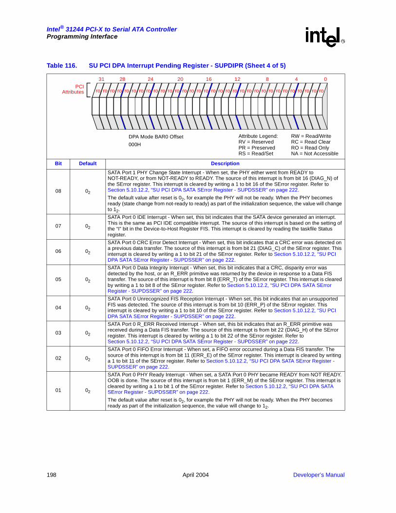
198 April 2004 Developer’s Manual
Intel® 31244 PCI-X to Serial ATA ControllerProgramming Interface
08 02
SATA Port 1 PHY Change State Interrupt - When set, the PHY either went from READY to NOT-READY, or from NOT-READY to READY. The source of this interrupt is from bit 16 (DIAG_N) of the SError register. This interrupt is cleared by writing a 1 to bit 16 of the SError register. Refer to Section 5.10.12.2, “SU PCI DPA SATA SError Register - SUPDSSER” on page 222.
The default value after reset is 02, for example the PHY will not be ready. When the PHY becomes ready (state change from not-ready to ready) as part of the initialization sequence, the value will change to 12.
07 02
SATA Port 0 IDE Interrupt - When set, this bit indicates that the SATA device generated an interrupt. This is the same as PCI IDE compatible interrupt. The source of this interrupt is based on the setting of the “I” bit in the Device-to-Host Register FIS. This interrupt is cleared by reading the taskfile Status register.
06 02
SATA Port 0 CRC Error Detect Interrupt - When set, this bit indicates that a CRC error was detected on a previous data transfer. The source of this interrupt is from bit 21 (DIAG_C) of the SError register. This interrupt is cleared by writing a 1 to bit 21 of the SError register. Refer to Section 5.10.12.2, “SU PCI DPA SATA SError Register - SUPDSSER” on page 222.
05 02
SATA Port 0 Data Integrity Interrupt - When set, this bit indicates that a CRC, disparity error was detected by the host, or an R_ERR primitive was returned by the device in response to a Data FIS transfer. The source of this interrupt is from bit 8 (ERR_T) of the SError register. This interrupt is cleared by writing a 1 to bit 8 of the SError register. Refer to Section 5.10.12.2, “SU PCI DPA SATA SError Register - SUPDSSER” on page 222.
04 02
SATA Port 0 Unrecognized FIS Reception Interrupt - When set, this bit indicates that an unsupported FIS was detected. The source of this interrupt is from bit 10 (ERR_P) of the SError register. This interrupt is cleared by writing a 1 to bit 10 of the SError register. Refer to Section 5.10.12.2, “SU PCI DPA SATA SError Register - SUPDSSER” on page 222.
03 02
SATA Port 0 R_ERR Received Interrupt - When set, this bit indicates that an R_ERR primitive was received during a Data FIS transfer. The source of this interrupt is from bit 22 (DIAG_H) of the SError register. This interrupt is cleared by writing a 1 to bit 22 of the SError register. Refer to Section 5.10.12.2, “SU PCI DPA SATA SError Register - SUPDSSER” on page 222.
02 02
SATA Port 0 FIFO Error Interrupt - When set, a FIFO error occurred during a Data FIS transfer. The source of this interrupt is from bit 11 (ERR_E) of the SError register. This interrupt is cleared by writing a 1 to bit 11 of the SError register. Refer to Section 5.10.12.2, “SU PCI DPA SATA SError Register - SUPDSSER” on page 222.
01 02
SATA Port 0 PHY Ready Interrupt - When set, a SATA Port 0 PHY became READY from NOT READY. OOB is done. The source of this interrupt is from bit 1 (ERR_M) of the SError register. This interrupt is cleared by writing a 1 to bit 1 of the SError register. Refer to Section 5.10.12.2, “SU PCI DPA SATA SError Register - SUPDSSER” on page 222.
The default value after reset is 02, for example the PHY will not be ready. When the PHY becomes ready as part of the initialization sequence, the value will change to 12.
Table 116. SU PCI DPA Interrupt Pending Register - SUPDIPR (Sheet 4 of 5)
Bit Default Description
PCIAttributes
28 24 20 16 12 8 4 031
ro ro ro ro ro ro ro ro ro ro ro ro ro ro ro ro ro ro ro ro ro ro ro ro ro ro ro ro ro ro ro ro
Attribute Legend:RV = ReservedPR = PreservedRS = Read/Set
RW = Read/WriteRC = Read ClearRO = Read OnlyNA = Not Accessible
DPA Mode BAR0 Offset
000H
Developer’s Manual April 2004 199
Intel® 31244 PCI-X to Serial ATA ControllerProgramming Interface
00 02
SATA Port 0 PHY Change State Interrupt - When set, the PHY either went from READY to NOT-READY, or from NOT-READY to READY. The source of this interrupt is from bit 16 (DIAG_N) of the SError register. This interrupt is cleared by writing a 1 to bit 16 of the SError register. Refer to Section 5.10.12.2, “SU PCI DPA SATA SError Register - SUPDSSER” on page 222.
The default value after reset is 02, for example the PHY will not be ready. When the PHY becomes ready (state change from not-ready to ready) as part of the initialization sequence, the value will change to 12.
Table 116. SU PCI DPA Interrupt Pending Register - SUPDIPR (Sheet 5 of 5)
Bit Default Description
PCIAttributes
28 24 20 16 12 8 4 031
ro ro ro ro ro ro ro ro ro ro ro ro ro ro ro ro ro ro ro ro ro ro ro ro ro ro ro ro ro ro ro ro
Attribute Legend:RV = ReservedPR = PreservedRS = Read/Set
RW = Read/WriteRC = Read ClearRO = Read OnlyNA = Not Accessible
DPA Mode BAR0 Offset
000H

200 April 2004 Developer’s Manual
Intel® 31244 PCI-X to Serial ATA ControllerProgramming Interface
5.10.8.2 SU PCI DPA Interrupt Mask Register - SUPDIMR
The SU PCI DPA Interrupt Mask Register is a 32-bit register. This register is used to mask interrupts pending in the SU PCI DPA Interrupt Pending Register. Each bit in the SU PCI DPA Interrupt Mask Register corresponds to a bit in the SU PCI DPA Interrupt Pending Register. Refer to Section 5.10.8.1, “SU PCI DPA Interrupt Pending Register - SUPDIPR” on page 194.
Table 117. SU PCI DPA Interrupt Mask Register - SUPDIMR (Sheet 1 of 3)
Bit Default Description
31 12
SATA Port 3 IDE Interrupt Mask Bit.
0 = Masked1 = Not Masked
30 02
SATA Port 3 Signal Detect Interrupt Mask Bit.
0 = Masked1 = Not Masked
29 02
SATA Port 3 Data Integrity Interrupt Mask Bit.
0 = Masked1 = Not Masked
28 02
SATA Port 3 Unrecognized FIS Reception Interrupt Mask Bit.
0 = Masked1 = Not Masked
27 02
SATA Port 3 R_ERR Primitive Received Interrupt Mask Bit.
0 = Masked1 = Not Masked
26 02
SATA Port 3 FIFO Error Interrupt Mask Bit.
0 = Masked1 = Not Masked
25 02
SATA Port 3 PHY Ready Interrupt Mask Bit.
0 = Masked1 = Not Masked
24 02
SATA Port 3 PHY Change State Interrupt Mask Bit.
0 = Masked1 = Not Masked
23 12
SATA Port 2 IDE Interrupt Mask Bit.
0 = Masked1 = Not Masked
22 02
SATA Port 2 Signal Detect Interrupt Mask Bit.
0 = Masked1 = Not Masked
PCIAttributes
28 24 20 16 12 8 4 031
rw rw rw rw rw rw rw rw rw rw rw rw rw rw rw rw rw rw rw rw rw rw rw rw rw rw rw rw rw rw rw rw
Attribute Legend:RV = ReservedPR = PreservedRS = Read/Set
RW = Read/WriteRC = Read ClearRO = Read OnlyNA = Not Accessible
DPA Mode BAR0 Offset
004H
Developer’s Manual April 2004 201
Intel® 31244 PCI-X to Serial ATA ControllerProgramming Interface
21 02
SATA Port 2 Data Integrity Interrupt Mask Bit.
0 = Masked1 = Not Masked
20 02
SATA Port 2 Unrecognized FIS Reception Interrupt Mask Bit.
0 = Masked1 = Not Masked
19 02
SATA Port 2 R_ERR Primitive Received Interrupt Mask Bit.
0 = Masked1 = Not Masked
18 02
SATA Port 2 FIFO Error Interrupt Mask Bit.
0 = Masked1 = Not Masked
17 02
SATA Port 2 PHY Ready Interrupt Mask Bit.
0 = Masked1 = Not Masked
16 02
SATA Port 2 PHY Change State Interrupt Mask Bit.
0 = Masked1 = Not Masked
15 12
SATA Port 1 IDE Interrupt Mask Bit.
0 = Masked1 = Not Masked
14 02
SATA Port 1 Signal Detect Interrupt Mask Bit.
0 = Masked1 = Not Masked
13 02
SATA Port 1 Data Integrity Interrupt Mask Bit.
0 = Masked1 = Not Masked
12 02
SATA Port 1 Unrecognized FIS Reception Interrupt Mask Bit.
0 = Masked1 = Not Masked
11 02
SATA Port 1 R_ERR Primitive Received Interrupt Mask Bit.
0 = Masked1 = Not Masked
10 02
SATA Port 1 FIFO Error Interrupt Mask Bit.
0 = Masked1 = Not Masked
Table 117. SU PCI DPA Interrupt Mask Register - SUPDIMR (Sheet 2 of 3)
Bit Default Description
PCIAttributes
28 24 20 16 12 8 4 031
rw rw rw rw rw rw rw rw rw rw rw rw rw rw rw rw rw rw rw rw rw rw rw rw rw rw rw rw rw rw rw rw
Attribute Legend:RV = ReservedPR = PreservedRS = Read/Set
RW = Read/WriteRC = Read ClearRO = Read OnlyNA = Not Accessible
DPA Mode BAR0 Offset
004H

202 April 2004 Developer’s Manual
Intel® 31244 PCI-X to Serial ATA ControllerProgramming Interface
09 02
SATA Port 1 PHY Ready Interrupt Mask Bit.
0 = Masked1 = Not Masked
08 02
SATA Port 1 PHY Change State Interrupt Mask Bit.
0 = Masked1 = Not Masked
07 12
SATA Port 0 IDE Interrupt Mask Bit.
0 = Masked1 = Not Masked
06 02
SATA Port 0 Signal Detect Interrupt Mask Bit.
0 = Masked1 = Not Masked
05 02
SATA Port 0 Data Integrity Interrupt Mask Bit.
0 = Masked1 = Not Masked
04 02
SATA Port 0 Unrecognized FIS Reception Interrupt Mask Bit.
0 = Masked1 = Not Masked
03 02
SATA Port 0 R_ERR Primitive Received Interrupt Mask Bit.
0 = Masked1 = Not Masked
02 02
SATA Port 0 FIFO Error Interrupt Mask Bit.
0 = Masked1 = Not Masked
01 02
SATA Port 0 PHY Ready Interrupt Mask Bit.
0 = Masked1 = Not Masked
00 02
SATA Port 0 PHY Change State Interrupt Mask Bit.
0 = Masked1 = Not Masked
Table 117. SU PCI DPA Interrupt Mask Register - SUPDIMR (Sheet 3 of 3)
Bit Default Description
PCIAttributes
28 24 20 16 12 8 4 031
rw rw rw rw rw rw rw rw rw rw rw rw rw rw rw rw rw rw rw rw rw rw rw rw rw rw rw rw rw rw rw rw
Attribute Legend:RV = ReservedPR = PreservedRS = Read/Set
RW = Read/WriteRC = Read ClearRO = Read OnlyNA = Not Accessible
DPA Mode BAR0 Offset
004H

Developer’s Manual April 2004 203
Intel® 31244 PCI-X to Serial ATA ControllerProgramming Interface
5.10.9 SU PCI DPA Mode Command Block Registers
This section defines the Command Block Registers when in DPA mode.
5.10.9.1 SU PCI DPA Data Port Register - SUPDDR
The SU PCI DPA Data Port Register is a 16-bit read/write register and is used to transfer data during Programmed I/O (PIO) mode reads/writes. On the GD31244 controller, the Data Port register may also be read or written as a 32-bit Data Port. The GD31244 controller internally breaks the 32-bit transaction into two back-to-back 16-bit transactions. It is recommended that the Data Port register is always accessed with either 16-bit or 32-bit quantity for a given PIO sequence. Refer to the AT Attachment with Packet Interface-6 (ATA/ATAPI-6) Specification.
.
Table 118. SU PCI DPA Data Port Register - SUPDDR
Bit Default Description
15:00 0000H Data Port - This register is used to transfer data during PIO reads and writes. This register shall be accessed only when the DRQ bit in the SU PCI DPA Status Register - SUPDSR is set.
PCIAttributes
15 12 8 4 0
rw rw rw rw rw rw rw rw rw rw rw rw rw rw rw rw
Attribute Legend:RV = ReservedPR = PreservedRS = Read/Set
RW = Read/WriteRC = Read ClearRO = Read OnlyNA = Not Accessible
DPA Mode BAR0 Offset
Port 0 = 200H, Port 1 = 400H
Port 2 = 600H, Port 3 = 800H

204 April 2004 Developer’s Manual
Intel® 31244 PCI-X to Serial ATA ControllerProgramming Interface
5.10.9.2 SU PCI DPA Error Register - SUPDER
The SU PCI DPA Error Register is a 8-bit read-only register. The SU PCI DPA Error Register contains error status for the current command. The content of this register shall be valid when the ERR bit is set in the SU PCI DPA Status Register - SUPDSR. The SU PCI DPA Error Register is command dependent and the bits are defined in the AT Attachment with Packet Interface-6 (ATA/ATAPI-6) Specification.
Table 119. SU PCI DPA Error Register - SUPDER
Bit Default Description
07:00 Device Dependent a
a. After a hardware reset, software reset, or an EXECUTE DEVICE DIAGNOSTIC command, the device will return a diagnostic code. The diagnosticcode is device dependent. Refer to the AT Attachment with Packet Interface-6 (ATA/ATAPI-6) Specification.
The bits in this register are command dependent. The bits are only valid when the ERR bit (bit 0) in the SU PCI DPA Status Register - SUPDSR is set. Refer to the AT Attachment with Packet Interface-6 (ATA/ATAPI-6) Specification.
PCIAttributes
7 4 0
ro ro ro ro ro ro ro ro
3
Attribute Legend:RV = ReservedPR = PreservedRS = Read/Set
RW = Read/WriteRC = Read ClearRO = Read OnlyNA = Not Accessible
DPA Mode BAR0 Offset
Port 0 = 204H, Port 1 = 404H
Port 2 = 604H, Port 3 = 804H
Developer’s Manual April 2004 205
Intel® 31244 PCI-X to Serial ATA ControllerProgramming Interface
5.10.9.3 SU PCI DPA Features Register - SUPDFR
The SU PCI DPA Features Register is a 16-bit register. The content of the SU PCI DPA Features Register is a command parameter. The content of this register must be loaded before the SU PCI DPA Command Register is written. The content of the SU PCI DPA Features Register is command dependent. Refer to the AT Attachment with Packet Interface-6 (ATA/ATAPI-6) Specification.
Table 120. SU PCI DPA Features Register - SUPDFR
Bit Default Description
15:00 00H Features - This register is command dependent. For example, it may be a parameter as an extension to the IDE Command Register.
PCIAttributes
15 12 8 4 0
rw rw rw rw rw rw rw rw rw rw rw rw rw rw rw rw
Attribute Legend:RV = ReservedPR = PreservedRS = Read/Set
WO = Write Only
RW = Read/WriteRC = Read ClearRO = Read OnlyNA = Not Accessible
DPA Mode BAR0 Offset
Port 0 = 206H, Port 1 = 406H
Port 2 = 606H, Port 3 = 806H

206 April 2004 Developer’s Manual
Intel® 31244 PCI-X to Serial ATA ControllerProgramming Interface
5.10.9.4 SU PCI DPA Sector Count Register - SUPDSCR
The SU PCI DPA Sector Count Register is a 16-bit read/write register. The content of the SU PCI DPA Sector Count Register is a command parameter. The content of this register must be loaded before the SU PCI DPA Command Register is written. The content of the SU PCI DPA Sector Count Register is command dependent. Refer to the AT Attachment with Packet Interface-6 (ATA/ATAPI-6) Specification.
Table 121. SU PCI DPA Sector Count Register - SUPDSCR
Bit Default Description
15:00 Device Dependent a
a. After a hardware reset, software reset, or an EXECUTE DEVICE DIAGNOSTIC command, the device will return a signature value. The signaturevalue is device dependent. Refer to the AT Attachment with Packet Interface-6 (ATA/ATAPI-6) Specification.
Sector Count/LBA Low:
• CHS addressing - only the lower byte is used for specifying a sector count.
• 28-bit LBA addressing - only the lower byte is used for specifying a sector count.
• 48-bit LBA addressing - a 16-bit value is used for specifying a sector count.
PCIAttributes
15 12 8 4 0
rw rw rw rw rw rw rw rw rw rw rw rw rw rw rw rw
Attribute Legend:RV = ReservedPR = PreservedRS = Read/Set
RW = Read/WriteRC = Read ClearRO = Read OnlyNA = Not Accessible
DPA Mode BAR0 Offset
Port 0 = 208H, Port 1 = 408H
Port 2 = 608H, Port 3 = 808H
Developer’s Manual April 2004 207
Intel® 31244 PCI-X to Serial ATA ControllerProgramming Interface
5.10.9.5 SU PCI DPA Sector Number Register - SUPDSNR
The SU PCI DPA Sector Number Register is a 16-bit read/write register. The content of the SU PCI DPA Sector Number Register is a command parameter. The content of this register must be loaded before the SU PCI DPA Command Register is written. The content of this register is command dependent. Refer to the AT Attachment with Packet Interface-6 (ATA/ATAPI-6) Specification.
Table 122. SU PCI DPA Sector Number Register - SUPDSNR
Bit Default Description
15:00 Device Dependent a
a. After a hardware reset, software reset, or an EXECUTE DEVICE DIAGNOSTIC command, the device will return a signature value. The signaturevalue is device dependent. Refer to the AT Attachment with Packet Interface-6 (ATA/ATAPI-6) Specification.
Sector Number/LBA Low- This field is dependent on the device access methods. There are three method:
• CHS addressing: This field indicates the device sector number to request as part of the Cylinder/Head/Sector format.
• 28-bit LBA addressing: This lower eight bits of this field is used for bit positions LBA[7:0] of the 28-bit address LBA[27:0].
• 48-bit LBA addressing: This upper and lower bytes of this field is used for bit positions LBA[31:24] and LBA[7:0] respectively of the 48-bit addressing LBA[47:0].
PCIAttributes
15 12 8 4 0
rw rw rw rw rw rw rw rw rw rw rw rw rw rw rw rw
Attribute Legend:RV = ReservedPR = PreservedRS = Read/Set
RW = Read/WriteRC = Read ClearRO = Read OnlyNA = Not Accessible
DPA Mode BAR0 Offset
Port 0 = 20CH, Port 1 = 40CH
Port 2 = 60CH, Port 3 = 80CH

208 April 2004 Developer’s Manual
Intel® 31244 PCI-X to Serial ATA ControllerProgramming Interface
5.10.9.6 SU PCI DPA Cylinder Low Register - SUPDCLR
The SU PCI DPA Cylinder Low Register is a 16-bit read/write register. The content of the SU PCI DPA Cylinder Low Register is a command parameter. The content of this register must be loaded before the SU PCI DPA Command Register is written. The content of the SU PCI DPA Cylinder Low Register is command dependent. Refer to the AT Attachment with Packet Interface-6 (ATA/ATAPI-6) Specification.
Table 123. SU PCI DPA Cylinder Low Register - SUPDCLR
Bit Default Description
15:00 Device Dependent a
a. After a hardware reset, software reset, or an EXECUTE DEVICE DIAGNOSTIC command, the device will return a signature value. The signaturevalue is device dependent. Refer to the AT Attachment with Packet Interface-6 (ATA/ATAPI-6) Specification.
Cylinder Low/LBA Mid - This field is dependent on the device access methods. There are three method:
• CHS addressing: This field indicates the lower cylinder byte to request as part of the Cylinder/Head/Sector format.
• 28-bit LBA addressing: This lower eight bits of this field is used for bit positions LBA[15:8] of the 28-bit address LBA[27:0].
• 48-bit LBA addressing: This upper and lower bytes of this field is used for bit positions LBA[39:32] and LBA[15:8] respectively of the 48-bit addressing LBA[47:0].
PCIAttributes
15 12 8 4 0
rw rw rw rw rw rw rw rw rw rw rw rw rw rw rw rw
Attribute Legend:RV = ReservedPR = PreservedRS = Read/Set
RW = Read/WriteRC = Read ClearRO = Read OnlyNA = Not Accessible
DPA Mode BAR0 Offset
Port 0 = 210H, Port 1 = 410H
Port 2 = 610H, Port 3 = 810H

Developer’s Manual April 2004 209
Intel® 31244 PCI-X to Serial ATA ControllerProgramming Interface
5.10.9.7 SU PCI DPA Cylinder High Register - SUPDCHR
The SU PCI DPA Cylinder High Register is a 16-bit read/write register. The content of the SU PCI DPA Cylinder High Register is a command parameter. The content of this register must be loaded before the SU PCI DPA Command Register is written. The content of the SU PCI DPA Cylinder High Register is command dependent. Refer to the AT Attachment with Packet Interface-6 (ATA/ATAPI-6) Specification.
Table 124. SU PCI DPA Cylinder High Register - SUPDCHR
Bit Default Description
15:00 Device Dependent a
a. After a hardware reset, software reset, or an EXECUTE DEVICE DIAGNOSTIC command, the device will return a signature value. The signaturevalue is device dependent. Refer to the AT Attachment with Packet Interface-6 (ATA/ATAPI-6) Specification.
Cylinder High/LBA High - This field is dependent on the device access methods. There are three method:
• CHS addressing: This field specifies the higher cylinder byte to request as part of the Cylinder/Head/Sector format.
• 28-bit LBA addressing: This lower eight bits of this field is used for bit positions LBA[23:16] of the 28-bit address LBA[27:0].
• 48-bit LBA addressing: The upper and lower bytes of this field is used for bit positions LBA[47:40] and LBA[23:16] respectively of the 48-bit addressing LBA[47:0].
PCIAttributes
15 12 8 4 0
rw rw rw rw rw rw rw rw rw rw rw rw rw rw rw rw
Attribute Legend:RV = ReservedPR = PreservedRS = Read/Set
RW = Read/WriteRC = Read ClearRO = Read OnlyNA = Not Accessible
DPA Mode BAR0 Offset
Port 0 = 214H, Port 1 = 414H
Port 2 = 614H, Port 3 = 814H

210 April 2004 Developer’s Manual
Intel® 31244 PCI-X to Serial ATA ControllerProgramming Interface
5.10.9.8 SU PCI DPA Device/Head Register - SUPDDR
This SU PCI DPA Device/Head Register is an 8-bit read/write register. The content of the SU PCI DPA Device/Head Register is a command parameter. The content of this register must be loaded before the SU PCI DPA Command Register is written. The content of the SU PCI DPA Device/Head Register is command dependent. Refer to the AT Attachment with Packet Interface-6 (ATA/ATAPI-6) Specification.
Table 125. SU PCI DPA Device/Head Register - SUPDDHR
Bit Default Description
07
Device Dependent a
a. After a hardware reset, software reset, or an EXECUTE DEVICE DIAGNOSTIC command, the device will return a signature value. The signaturevalue is device dependent. Refer to the AT Attachment with Packet Interface-6 (ATA/ATAPI-6) Specification.
Reserved
06Logical Addressing Mode - This bit indicates the addressing mode:
0 = CHS Mode1 = LBA Mode
05 Reserved
04 Reserved.
03:00
Head - This field is dependent on the device access methods. There are three methods:
• CHS addressing: this field indicates the head number for the Cylinder/Head/Sector format.
• 28-bit LBA addressing: This field is used for bit positions LBA[27:24] of the 28-bit addressing LBA[27:0].
• 48-bit LBA Mode: These bit are not part of the 48-bit LBA address, but need to be set to 11112.
PCIAttributes
7 4 0
rv rw rv rv rw rw rw rw
Attribute Legend:RV = ReservedPR = PreservedRS = Read/Set
RW = Read/WriteRC = Read ClearRO = Read OnlyNA = Not Accessible
DPA Mode BAR0 Offset
Port 0 = 218H, Port 1 = 418H
Port 2 = 618H, Port 3 = 818H

Developer’s Manual April 2004 211
Intel® 31244 PCI-X to Serial ATA ControllerProgramming Interface
5.10.9.9 SU PCI DPA Status Register - SUPDSR
The SU PCI DPA Status Register is an 8-bit read-only register. This register provides the status of the device and the interface. Reading this register implicitly clears any pending interrupt. Instead, the Alternate Status register may be used to read the status of a device without causing any pending interrupt to get cleared. Some of the bits in this register are command-dependent and are described in the AT Attachment with Packet Interface-6 (ATA/ATAPI-6) Specification. Information in this register is updated by the device sending a Device-to-Host Register FIS or PIO Setup FIS.
Table 126. SU PCI DPA Status Register - SUPDSR
Bit Default Description
07
Device Dependent a
a. After power-on, a value of 7FH is returned in this register when read before a device is detected on the serial link. This is consistent with the ATAstandard, indicating that a device is not connected to the cable. After the device is detected and a communication link is established between thehost and the device, a value of 80H will be read. Bit 7 (BSY bit) set indicates that the device has been detected, but is busy executing itsinitialization and diagnostics. After the device is done with its initialization and diagnostics sequence, it will send a Device-to-Host Register FISwith bit 7 (BSY bit) cleared.
BSY - When this bit is set the interface/device is busy. For example, the device may be working a previous command. This bit is set immediately after the Command register is written and a Host-to-Device Register FIS is sent to the device, indicating that the interface is busy. The device is then responsible to clear this bit by sending a PIO Setup FIS or Device-to-Host Register FIS.
06 DRDY - This bit when set indicates that the device is ready.
05 This bit is command dependent. Refer to the AT Attachment with Packet Interface-6 (ATA/ATAPI-6) Specification.
04 This bit is command dependent. Refer to the AT Attachment with Packet Interface-6 (ATA/ATAPI-6) Specification.
03 DRQ - This bit is set when the device is ready to transfer data for PIO transactions.
02 This bit is command dependent. Refer to the AT Attachment with Packet Interface-6 (ATA/ATAPI-6) Specification.
01 This bit is command dependent. Refer to the AT Attachment with Packet Interface-6 (ATA/ATAPI-6) Specification.
00 ERR - This bit when set indicates that an error occurred. The SU PCI DPA Error Register - SUPDER provides further error information.
PCIAttributes
7 4 0
ro ro ro ro ro ro ro ro
3
Attribute Legend:RV = ReservedPR = PreservedRS = Read/Set
RW = Read/WriteRC = Read ClearRO = Read OnlyNA = Not Accessible
DPA Mode BAR0 Offset
Port 0 = 21CH, Port 1 = 41CH
Port 2 = 61CH, Port 3 = 81CH
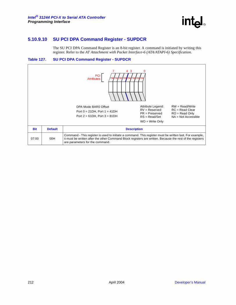
212 April 2004 Developer’s Manual
Intel® 31244 PCI-X to Serial ATA ControllerProgramming Interface
5.10.9.10 SU PCI DPA Command Register - SUPDCR
The SU PCI DPA Command Register is an 8-bit register. A command is initiated by writing this register. Refer to the AT Attachment with Packet Interface-6 (ATA/ATAPI-6) Specification.
Table 127. SU PCI DPA Command Register - SUPDCR
Bit Default Description
07:00 00HCommand - This register is used to initiate a command. This register must be written last. For example, it must be written after the other Command Block registers are written. Because the rest of the registers are parameters for the command.
PCIAttributes
7 4 0
rw rw rw rw rw rw rw rw
3
Attribute Legend:RV = ReservedPR = PreservedRS = Read/Set
WO = Write Only
RW = Read/WriteRC = Read ClearRO = Read OnlyNA = Not Accessible
DPA Mode BAR0 Offset
Port 0 = 21DH, Port 1 = 41DH
Port 2 = 61DH, Port 3 = 81DH
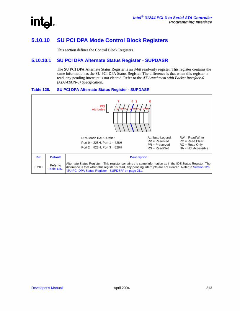
Developer’s Manual April 2004 213
Intel® 31244 PCI-X to Serial ATA ControllerProgramming Interface
5.10.10 SU PCI DPA Mode Control Block Registers
This section defines the Control Block Registers.
5.10.10.1 SU PCI DPA Alternate Status Register - SUPDASR
The SU PCI DPA Alternate Status Register is an 8-bit read-only register. This register contains the same information as the SU PCI DPA Status Register. The difference is that when this register is read, any pending interrupt is not cleared. Refer to the AT Attachment with Packet Interface-6 (ATA/ATAPI-6) Specification.
Table 128. SU PCI DPA Alternate Status Register - SUPDASR
Bit Default Description
07:00 Refer to Table 126.
Alternate Status Register - This register contains the same information as in the IDE Status Register. The difference is that when this register is read, any pending interrupts are not cleared. Refer to Section 126, “SU PCI DPA Status Register - SUPDSR” on page 211.
PCIAttributes
7 4 0
ro ro ro ro ro ro ro ro
3
Attribute Legend:RV = ReservedPR = PreservedRS = Read/Set
RW = Read/WriteRC = Read ClearRO = Read OnlyNA = Not Accessible
DPA Mode BAR0 Offset
Port 0 = 228H, Port 1 = 428H
Port 2 = 628H, Port 3 = 828H

214 April 2004 Developer’s Manual
Intel® 31244 PCI-X to Serial ATA ControllerProgramming Interface
5.10.10.2 SU PCI DPA Device Control Register - SUPDDCTLR
The SU PCI DPA Device Control Register is an 8-bit write-only register. The SU PCI DPA Device Control Register is used to initiate a software reset to the device. Refer to the AT Attachment with Packet Interface-6 (ATA/ATAPI-6) Specification.
Table 129. SU PCI DPA Device Control Register - SUPDDCTLR
Bit Default Description
07 02 Reserved.
06 02 Reserved.
05 02 Reserved.
04 02 Reserved.
03 02 Reserved.
02 02SRST - This bit is used by software to perform a device reset. Writing a 1 requests the device to start the reset sequence, and writing a 0 request the device to terminate reset.
01 02 Reserved.
00 02 Reserved. This bit shall always be cleared.
PCIAttributes
7 4 0
rv rv rv rv rv wo rv rv
3
Attribute Legend:RV = ReservedPR = PreservedRS = Read/SetWO = Write Only
RW = Read/WriteRC = Read ClearRO = Read OnlyNA = Not Accessible
DPA Mode BAR0 Offset
Port 0 = 229H, Port 1 = 429H
Port 2 = 629H, Port 3 = 829H

Developer’s Manual April 2004 215
Intel® 31244 PCI-X to Serial ATA ControllerProgramming Interface
5.10.11 SU PCI DPA Mode DMA Registers
This section defines the DPA DMA Registers.
5.10.11.1 SU PCI DPA Upper DMA Descriptor Table Pointer Register - SUPDUDDTPR
The SU PCI DPA Upper DMA Descriptor Table Pointer Register contains the upper 32-bit PCI address of the 64-bit PCI address. In PCI IDE mode, the SU PCI DPA Upper DMA Descriptor Table Pointer Register is not used. This register allows the descriptor table to be located in any 4 Gbyte memory space.
Table 130. SU PCI DPA Upper DMA Descriptor Table Pointer Register - SUPDUDDTPR
Bit Default Description
31:00 0000 0000H PCI Address - is the PCI source/destination upper address.
PCIAttributes
28 24 20 16 12 8 4 031
rw rw rw rw rw rw rw rw rw rw rw rw rw rw rw rw rw rw rw rw rw rw rw rw rw rw rw rw rw rw rw rw
Attribute Legend:RV = ReservedPR = PreservedRS = Read/Set
RW = Read/WriteRC = Read ClearRO = Read OnlyNA = Not Accessible
DPA Mode BAR0 Offset
Port 0 = 264H, Port 1 = 464H
Port 2 = 664H, Port 3 = 864H

216 April 2004 Developer’s Manual
Intel® 31244 PCI-X to Serial ATA ControllerProgramming Interface
5.10.11.2 SU PCI DPA Upper DMA Data Pointer Register - SUPDUDDBPR
This SU PCI DPA Upper DMA Data Pointer Register contains the upper 32-bit PCI address of the 64-bit PCI address. All the descriptors in the descriptor table share this register. For example, all the data buffers must be located in the same 4 Gbyte memory space.
Table 131. SU PCI DPA Upper DMA Data Buffer Pointer Register - SUPDUDDPR
Bit Default Description
31:00 0000 0000H PCI Address - The PCI source/destination upper address.
PCIAttributes
28 24 20 16 12 8 4 031
rw rw rw rw rw rw rw rw rw rw rw rw rw rw rw rw rw rw rw rw rw rw rw rw rw rw rw rw rw rw rw rw
Attribute Legend:RV = ReservedPR = PreservedRS = Read/Set
RW = Read/WriteRC = Read ClearRO = Read OnlyNA = Not Accessible
DPA Mode BAR0 Offset
Port 0 = 26CH, Port 1 = 46CH
Port 2 = 66CH, Port 3 = 86CH

Developer’s Manual April 2004 217
Intel® 31244 PCI-X to Serial ATA ControllerProgramming Interface
5.10.11.3 SU PCI DPA DMA Command Register - SUPDDCMDR
The SU PCI DPA DMA Command Register enables/disables the DMA engine (bus master capability) and also provides direction control for DMA transfers.
.
Table 132. SU PCI DPA DMA Command Register - SUPDDCMDR
Bit Default Description
15:10 00H Reserved
09 02
First Party DMA Direction:
0 = From Device to Host1 = From Host to Device
08 02
First Party DMA Active:
0 = Not Active1 = Active
07:04 0H Reserved
03 02
DMA Read/Write Control:
0 = Reads Memory to write FIFO. FIFO data is written to SATA device.1 = Writes Memory with FIFO data. FIFO contains data read from SATA device.
This bit must NOT be changed when the DMA is active. While synchronous DMA transfer is in progress, this bit will be READ ONLY. The bit will return to read/write once the synchronous DMA transfer has been completed or halted.
02:01 002 Reserved.
00 02
Start/Stop DMA Transfer: 1 = Start; 0 = Stop. When this bit is set to 1, the DMA operation starts. The controller transfers data between the device and memory only while this bit is set. Operation may be stopped by writing a 0 to this bit. This results in all state information being lost (i.e., operation cannot be stop and then resumed).
When this bit is set to 0 while bus master operation is still active (i.e., bit 0 = 1 in the DMA Status Register) and data transfer has not yet finished (i.e., bit 2 = 0 in the DMA Status Register), the DMA command is aborted and data transferred from the drive may be discarded by the SATA port rather than being written to memory. This bit is intended to be set to 0 after the data transfer is completed, as indicated by either bit 0 or bit 2 set in the DMA Status Register.
PCIAttributes
15 12 8 4 0
rv rv rv rv rv rv ro ro rv rv rv rv rw rv rv rw
Attribute Legend:RV = ReservedPR = PreservedRS = Read/Set
RW = Read/WriteRC = Read ClearRO = Read OnlyNA = Not Accessible
DPA Mode BAR0 Offset
Port 0 = 270H, Port 1 = 470H
Port 2 = 670H, Port 3 = 870H

218 April 2004 Developer’s Manual
Intel® 31244 PCI-X to Serial ATA ControllerProgramming Interface
5.10.11.4 SU PCI DPA DMA Status Register - SUPDDSR
The SU PCI DPA DMA Status Register provides status of the DMA engine..
Table 133. SU PCI DPA DMA Status Register - SUPDDSR
Bit Default Description
07 02 This bit is hardwired to 0. Simplex only.
06 02 Reserved.
05 12DMA Capable: 1 = Capable of DMA transfers. This bit is a software controlled status bit that indicates DMA device capability and does not affect hardware operation.
04:03 002 Reserved.
02 02
Interrupt Status: This bit, when set to a 1, indicates when a device has asserted its interrupt line. When this bit is set to 1, all read data from the device has been transferred to memory and all write data has been transferred to the device. Software sets this bit to a 0 by writing a 1 to it.
01 02
DMA Error: This bit is set to 1 under the following conditions while transferring data on the PCI bus.
• Detected a master abort on the PCI bus
• Detected a target abort on the PCI bus
• Detected a parity error on the PCI bus
Software sets this bit to 0 by writing a 1 to it.
00 02
DMA Active: The GD31244 controller sets this bit to 1 when bit 0 in the SU PCI DPA DMA Command Register is set to 1. Refer to Section 5.10.11.3, “SU PCI DPA DMA Command Register - SUPDDCMDR” on page 217. The GD31244 controller sets this bit to 0 when the last transfer is performed (where EOT for that descriptor is set). The GD31244 controller also sets this bit to 0 when bit 0 of the IDE Channel 0 DMA Command Register is set to 0. When this bit is read as a 0, all data transferred from the drive during the previous bus master command is visible in memory, unless the DMA command was aborted.
PCIAttributes
7 4 03
ro rv rw rv rv rc rc ro
Attribute Legend:RV = ReservedPR = PreservedRS = Read/Set
RW = Read/WriteRC = Read ClearRO = Read OnlyNA = Not Accessible
DPA Mode BAR0 Offset
Port 0 = 272H, Port 1 = 472H
Port 2 = 672H, Port 3 = 872H

Developer’s Manual April 2004 219
Intel® 31244 PCI-X to Serial ATA ControllerProgramming Interface
5.10.11.5 SU PCI DPA DMA Descriptor Table Pointer Register - SUPDDDTPR
This SU PCI DPA DMA Descriptor Table Pointer Register contains the lower 32-bit PCI address. The SU PCI DPA DMA Descriptor Table Pointer Register points to system memory.
Table 134. SU PCI DPA DMA Descriptor Table Pointer Register - SUPDDDTPR
Bit Default Description
31:02 0000 0000H PCI Address - is lower PCI address. This register contains the base address of the descriptor table. The descriptor table must be DWORD aligned and must not cross a 64 Kbyte boundary.
01:00 002 Reserved.
PCIAttributes
28 24 20 16 12 8 4 031
rw rw rw rw rw rw rw rw rw rw rw rw rw rw rw rw rw rw rw rw rw rw rw rw rw rw rw rw rw rw rv rv
Attribute Legend:RV = ReservedPR = PreservedRS = Read/Set
RW = Read/WriteRC = Read ClearRO = Read OnlyNA = Not Accessible
DPA Mode BAR0 Offset
Port 0 = 274H, Port 1 = 474H
Port 2 = 674H, Port 3 = 874H

220 April 2004 Developer’s Manual
Intel® 31244 PCI-X to Serial ATA ControllerProgramming Interface
5.10.12 SU PCI DPA Mode Superset Registers
This section defines the Serial ATA Superset Registers. These registers provide control and status of the Serial ATA bus, and also support new Serial ATA specific commands.
5.10.12.1 SU PCI DPA SATA SStatus Register - SUPDSSSR
The SU PCI DPA SATA SStatus is a read-only register. The SU PCI DPA SATA SStatus Register provides status for the SATA interface itself, and conveys the interface state at the time it is read and is updated continuously and asynchronously. The SU PCI DPA SATA SStatus Register is one of the SCR Registers defined in the Serial ATA/High-Speed Serialized AT Attachment, Revision 1.0 RC-1.
Table 135. SU PCI DPA SATA SStatus Register - SUPDSSSR (Sheet 1 of 2)
Bit Default Description
31:12 0000_0H Reserved
11:08 00002
IPM - Interface Power Mode The IPM value indicates the current interface power management state
00002 - Device is not present or communication has not been established
00012 - Interface in active state
00102 - Interface in PARTIAL power management state
01102 - Interface in SLUMBER power management state
All other values are reserved.
The default value after reset is 00002. After communications between the host controller and the device is established, the value will change to reset 00012.
07:04 00002
SPD - The SPD value indicates the negotiated interface communication speed established
00002 - No negotiated speed because the device is not present or communication is not established
00012 - Generation 1 communication rate negotiated
All other values are reserved.
The default value after reset is 00002. After communications between the host controller and the device is established, the value will change to reset 00012.
PCIAttributes
28 24 20 16 12 8 4 031
rv rv rv rv rv rv rv rv rv rv rv rv rv rv rv rv rv rv rv rv ro ro ro ro ro ro ro ro ro ro ro ro
Attribute Legend:RV = ReservedPR = PreservedRS = Read/Set
RW = Read/WriteRC = Read ClearRO = Read OnlyNA = Not Accessible
PCI IDE Mode BAR5 Offset
= 000H,
DPA Mode BAR0 DPA Mode Offset
Port 0 = 300H, Port 1 = 500H
Port 2 = 700H, Port 3 = 900H
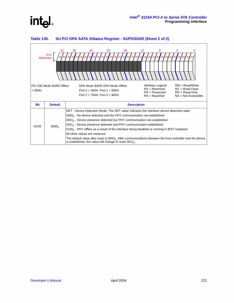
Developer’s Manual April 2004 221
Intel® 31244 PCI-X to Serial ATA ControllerProgramming Interface
03:00 00002
DET - Device Detection Mode: The DET value indicates the interface device detection state
00002 - No device detected and the PHY communication not established
00012 - Device presence detected but PHY communication not established
00112 - Device presence detected and PHY communication established
01002 - PHY offline as a result of the interface being disabled or running in BIST loopback
All other values are reserved.
The default value after reset is 00002. After communications between the host controller and the device is established, the value will change to reset 00112.
Table 135. SU PCI DPA SATA SStatus Register - SUPDSSSR (Sheet 2 of 2)
Bit Default Description
PCIAttributes
28 24 20 16 12 8 4 031
rv rv rv rv rv rv rv rv rv rv rv rv rv rv rv rv rv rv rv rv ro ro ro ro ro ro ro ro ro ro ro ro
Attribute Legend:RV = ReservedPR = PreservedRS = Read/Set
RW = Read/WriteRC = Read ClearRO = Read OnlyNA = Not Accessible
PCI IDE Mode BAR5 Offset
= 000H,
DPA Mode BAR0 DPA Mode Offset
Port 0 = 300H, Port 1 = 500H
Port 2 = 700H, Port 3 = 900H
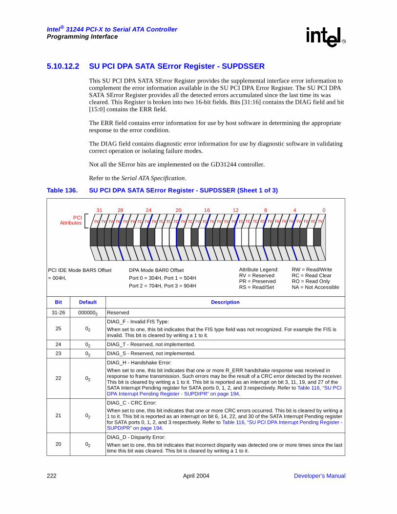
222 April 2004 Developer’s Manual
Intel® 31244 PCI-X to Serial ATA ControllerProgramming Interface
5.10.12.2 SU PCI DPA SATA SError Register - SUPDSSER
This SU PCI DPA SATA SError Register provides the supplemental interface error information to complement the error information available in the SU PCI DPA Error Register. The SU PCI DPA SATA SError Register provides all the detected errors accumulated since the last time its was cleared. This Register is broken into two 16-bit fields. Bits [31:16] contains the DIAG field and bit [15:0] contains the ERR field.
The ERR field contains error information for use by host software in determining the appropriate response to the error condition.
The DIAG field contains diagnostic error information for use by diagnostic software in validating correct operation or isolating failure modes.
Not all the SError bits are implemented on the GD31244 controller.
Refer to the Serial ATA Specification.
Table 136. SU PCI DPA SATA SError Register - SUPDSSER (Sheet 1 of 3)
Bit Default Description
31-26 0000002 Reserved
25 02
DIAG_F - Invalid FIS Type:
When set to one, this bit indicates that the FIS type field was not recognized. For example the FIS is invalid. This bit is cleared by writing a 1 to it.
24 02 DIAG_T - Reserved, not implemented.
23 02 DIAG_S - Reserved, not implemented.
22 02
DIAG_H - Handshake Error:
When set to one, this bit indicates that one or more R_ERR handshake response was received in response to frame transmission. Such errors may be the result of a CRC error detected by the receiver. This bit is cleared by writing a 1 to it. This bit is reported as an interrupt on bit 3, 11, 19, and 27 of the SATA Interrupt Pending register for SATA ports 0, 1, 2, and 3 respectively. Refer to Table 116, “SU PCI DPA Interrupt Pending Register - SUPDIPR” on page 194.
21 02
DIAG_C - CRC Error:
When set to one, this bit indicates that one or more CRC errors occurred. This bit is cleared by writing a 1 to it. This bit is reported as an interrupt on bit 6, 14, 22, and 30 of the SATA Interrupt Pending register for SATA ports 0, 1, 2, and 3 respectively. Refer to Table 116, “SU PCI DPA Interrupt Pending Register - SUPDIPR” on page 194.
20 02
DIAG_D - Disparity Error:
When set to one, this bit indicates that incorrect disparity was detected one or more times since the last time this bit was cleared. This bit is cleared by writing a 1 to it.
PCIAttributes
28 24 20 16 12 8 4 031
rv rv rv rv rv rv rc rv rv rc rc rc rv rc rv rc rv rv rv rv rc rc rc rc rv rv rv rv rv rv rc rv
Attribute Legend:RV = ReservedPR = PreservedRS = Read/Set
RW = Read/WriteRC = Read ClearRO = Read OnlyNA = Not Accessible
PCI IDE Mode BAR5 Offset
= 004H,
DPA Mode BAR0 Offset
Port 0 = 304H, Port 1 = 504H
Port 2 = 704H, Port 3 = 904H

Developer’s Manual April 2004 223
Intel® 31244 PCI-X to Serial ATA ControllerProgramming Interface
19 02 DIAG_B - not implemented.
18 02
DIAG_W - Comm Wake:
When set to one, this bit indicates that a Comm Wake was detected by the PHY. This bit is cleared by writing a 1 to it. The default value after reset is 02. After Comm Wake is detected, the value will change to 12.
17 02 DIAG_I - Reserved, not implemented.
16 02
DIAG_N - PHYRDY Change State:
When set to one this bit indicates that the PHYRDY signal changed state. State change means going from READY to NOT-READY or NOT-READY to READY. This bit shall remain cleared when the PHY was not detected as ready during the initialization process. When the PHY goes ready after initialization, this bit shall transition to 1. This bit is cleared by writing a 1 to it. This bit is reported as an interrupt on bit 0, 8, 16, and 24 of the SATA Interrupt Pending register for SATA ports 0, 1, 2, and 3 respectively. Refer to Table 116, “SU PCI DPA Interrupt Pending Register - SUPDIPR” on page 194.
The default value after reset is 02, for example the PHY will not be ready. When the PHY becomes ready (state change from not-ready to ready) as part of the initialization sequence, the value will change to 12.
15-12 00002 Reserved.
11 02
ERR_E - Internal Error:
This bit indicates that a FIFO error occurred due to a FIFO overrun or underrun condition. This bit is cleared by writing a 1 to it. This bit is reported as an interrupt on bit 2, 10, 18, and 26 of the SATA Interrupt Pending register for SATA ports 0, 1, 2, and 3 respectively. Refer to Table 116, “SU PCI DPA Interrupt Pending Register - SUPDIPR” on page 194.
10 02
ERR_P - Protocol Error:
This bit when set indicates that a corrupted FIS was received. This bit may indicate that the FIS received was an invalid FIS type or that the received FIS was not properly structured. For example, incorrect length. This bit is cleared by writing a 1 to it. This bit is reported as an interrupt on bit 4, 12, 20, and 28 of the SATA Interrupt Pending register for SATA ports 0, 1, 2, and 3 respectively. Refer to Table 116, “SU PCI DPA Interrupt Pending Register - SUPDIPR” on page 194.
09
Varies with the signal
level of the PHY receive
path
ERR_C - Non-Recovered Communication:
This is an asynchronous signal which reflects the signal level of the PHY receive path. When high, this bit indicates that there is no signal detected on the PHY receive path (RX). This may occur from a faulty interconnect, removal of a device, or the signal level is simply below the reference point.
08 02
ERR_T - Non-Recovered Transient Data Integrity Error:
This bit indicates that either a CRC error, disparity error, or the receipt of an R_ERR primitive occurred in response to a Data FIS. This bit is cleared by writing a 1 to it. This bit is reported as an interrupt on bit 5, 13, 21, and 29 of the SATA Interrupt Pending register for SATA ports 0, 1, 2, and 3 respectively. Refer to Table 116, “SU PCI DPA Interrupt Pending Register - SUPDIPR” on page 194.
07:02 0000002 Reserved
Table 136. SU PCI DPA SATA SError Register - SUPDSSER (Sheet 2 of 3)
Bit Default Description
PCIAttributes
28 24 20 16 12 8 4 031
rv rv rv rv rv rv rc rv rv rc rc rc rv rc rv rc rv rv rv rv rc rc rc rc rv rv rv rv rv rv rc rv
Attribute Legend:RV = ReservedPR = PreservedRS = Read/Set
RW = Read/WriteRC = Read ClearRO = Read OnlyNA = Not Accessible
PCI IDE Mode BAR5 Offset
= 004H,
DPA Mode BAR0 Offset
Port 0 = 304H, Port 1 = 504H
Port 2 = 704H, Port 3 = 904H

224 April 2004 Developer’s Manual
Intel® 31244 PCI-X to Serial ATA ControllerProgramming Interface
01 02
ERR_M - Recovered Communications Error:
This bit indicates that the PHY went from NOT-READY to READY. This bit shall remain cleared when the PHY was not detected as ready during the initialization process. When the PHY goes ready after initialization, this bit shall transition to 1. This bit is cleared by writing a 1 to it. This bit is reported as an interrupt on bit 1, 9, 17, and 25 of the SATA Interrupt Pending register for SATA ports 0, 1, 2, and 3 respectively. Refer to Table 116, “SU PCI DPA Interrupt Pending Register - SUPDIPR” on page 194.
The default value after reset is 02, for example the PHY will not be ready. When the PHY becomes ready as part of the initialization sequence, the value will change to 12.
00 02 ERR_I - Reserved, not implemented.
Table 136. SU PCI DPA SATA SError Register - SUPDSSER (Sheet 3 of 3)
Bit Default Description
PCIAttributes
28 24 20 16 12 8 4 031
rv rv rv rv rv rv rc rv rv rc rc rc rv rc rv rc rv rv rv rv rc rc rc rc rv rv rv rv rv rv rc rv
Attribute Legend:RV = ReservedPR = PreservedRS = Read/Set
RW = Read/WriteRC = Read ClearRO = Read OnlyNA = Not Accessible
PCI IDE Mode BAR5 Offset
= 004H,
DPA Mode BAR0 Offset
Port 0 = 304H, Port 1 = 504H
Port 2 = 704H, Port 3 = 904H
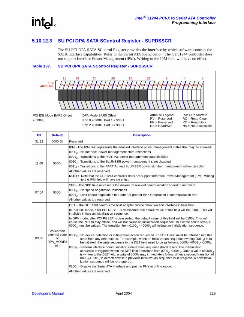
Developer’s Manual April 2004 225
Intel® 31244 PCI-X to Serial ATA ControllerProgramming Interface
5.10.12.3 SU PCI DPA SATA SControl Register - SUPDSSCR
The SU PCI DPA SATA SControl Register provides the interface by which software controls the SATA interface capabilities. Refer to the Serial ATA Specification. The GD31244 controller does not support Interface Power Management (IPM). Writing to the IPM field will have no effect.
Table 137. SU PCI DPA SATA SControl Register - SUPDSSCR
Bit Default Description
31:12 0000 0h Reserved
11:08 00002
IPM - The IPM field represents the enabled interface power management states that may be invoked:
00002 - No interface power management state restrictions
00012 - Transitions to the PARTIAL power management state disabled
00102 - Transitions to the SLUMBER power management state disabled
00112 - Transitions to the PARTIAL and SLUMBER power slumber management states disabled
All other values are reserved.
NOTE: Note that the GD31244 controller does not support Interface Power Management (IPM). Writing to the IPM field will have no effect.
07:04 00002
SPD - The SPD field represents the maximum allowed communication speed to negotiate
00002 - No speed negotiation restrictions
00012 - Limit speed negotiation to a rate not greater than Generation 1 communication rate
All other values are reserved.
03:00
Varies with external state
of DPA_MODE#
pin
DET - The DET field controls the host adapter device detection and interface initialization.
In PCI IDE mode, after PCI RESET is deasserted, the default value of this field will be 00002. This will implicitly initiate an initialization sequence.
In DPA mode, after PCI RESET is deasserted, the default value of this field will be 01002. This will cause the PHY to stay offline, and will not cause an initialization sequence. To exit the offline state, a 00002 must be written. The transition from 01002 -> 00002 will initiate an initialization sequence.
00002 - No device detection or initialization action requested. The DET field must be returned into this state from any other states. For example, when an initialization sequence (writing 00012) is to be initiated, the write sequence to the DET field need to be as follows: 00002->00012->00002.
00012 - Perform interface communication initialization sequence (hard reset). The initialization sequence is triggered when the DET field transitions from 00002->00012. Once a value of 00012 is written to the DET field, a write of 00002 may immediately follow. When a second transition of 00002->00012 is detected while a previous initialization sequence is in progress, a new initial-ization sequence will be re-triggered.
01002 - Disable the Serial ATA interface and put the PHY in offline mode.
All other values are reserved.
PCIAttributes
28 24 20 16 12 8 4 031
rv rv rv rv rv rv rv rv rv rv rv rv rv rv rv rv rv rv rv rv rw rw rw rw rw rw rw rw rw rw rw rw
Attribute Legend:RV = ReservedPR = PreservedRS = Read/Set
RW = Read/WriteRC = Read ClearRO = Read OnlyNA = Not Accessible
PCI IDE Mode BAR5 Offset
= 008H,
DPA Mode BAR0 Offset
Port 0 = 308H, Port 1 = 508H
Port 2 = 708H, Port 3 = 908H

226 April 2004 Developer’s Manual
Intel® 31244 PCI-X to Serial ATA ControllerProgramming Interface
5.10.12.4 SU PCI DPA Set Device Bits Register - SUPDSDBR
The SU PCI DPA Set Device Bits Register is a 32-bit register. This register reflects the content of the Set Device Bit FIS reserved DWORD.
Table 138. SU PCI DPA Set Device Bits Register - SUPDSDBR
Bit Default Description
31:00 0000_0000H
This is the SActive Register. The Serial ATA II Native Command Queueing specification defines this register as write read. Writing one to any bit will set the bait. The bits are cleared by the device set device bits FIS word 1 containing a 1 in that bit position. Writing a 0 to these bits by the host will not clear them.
PCIAttributes
28 24 20 16 12 8 4 031
rs rs rs rs rs rs rs rs rs rs rs rs rs rs rs rs rs rs rs rs rs rs rs rs rs rs rs rs rs rs rs rs
Attribute Legend:RV = ReservedPR = PreservedRS = Read/Set
RW = Read/WriteRC = Read ClearRO = Read OnlyNA = Not Accessible
PCI IDE Mode Offset
= 00CH,
DPA Mode BAR0 Offset
Port 0 = 30CH, Port 1 = 50CH
Port 2 = 70CH, Port 3 = 90CH
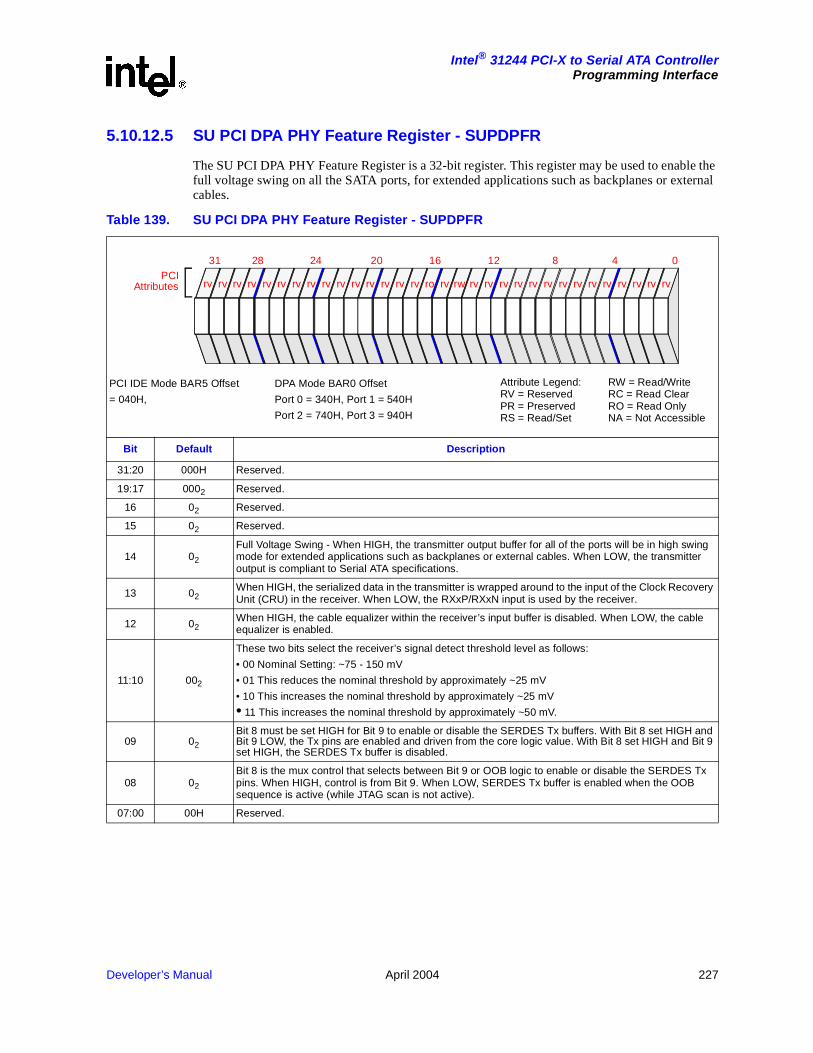
Developer’s Manual April 2004 227
Intel® 31244 PCI-X to Serial ATA ControllerProgramming Interface
5.10.12.5 SU PCI DPA PHY Feature Register - SUPDPFR
The SU PCI DPA PHY Feature Register is a 32-bit register. This register may be used to enable the full voltage swing on all the SATA ports, for extended applications such as backplanes or external cables.
Table 139. SU PCI DPA PHY Feature Register - SUPDPFR
Bit Default Description
31:20 000H Reserved.
19:17 0002 Reserved.
16 02 Reserved.
15 02 Reserved.
14 02
Full Voltage Swing - When HIGH, the transmitter output buffer for all of the ports will be in high swing mode for extended applications such as backplanes or external cables. When LOW, the transmitter output is compliant to Serial ATA specifications.
13 02When HIGH, the serialized data in the transmitter is wrapped around to the input of the Clock Recovery Unit (CRU) in the receiver. When LOW, the RXxP/RXxN input is used by the receiver.
12 02When HIGH, the cable equalizer within the receiver’s input buffer is disabled. When LOW, the cable equalizer is enabled.
11:10 002
These two bits select the receiver’s signal detect threshold level as follows:
• 00 Nominal Setting: ~75 - 150 mV
• 01 This reduces the nominal threshold by approximately ~25 mV
• 10 This increases the nominal threshold by approximately ~25 mV
• 11 This increases the nominal threshold by approximately ~50 mV.
09 02
Bit 8 must be set HIGH for Bit 9 to enable or disable the SERDES Tx buffers. With Bit 8 set HIGH and Bit 9 LOW, the Tx pins are enabled and driven from the core logic value. With Bit 8 set HIGH and Bit 9 set HIGH, the SERDES Tx buffer is disabled.
08 02
Bit 8 is the mux control that selects between Bit 9 or OOB logic to enable or disable the SERDES Tx pins. When HIGH, control is from Bit 9. When LOW, SERDES Tx buffer is enabled when the OOB sequence is active (while JTAG scan is not active).
07:00 00H Reserved.
PCIAttributes
28 24 20 16 12 8 4 031
rv rv rv rv rv rv rv rv rv rv rv rv rv rv rv ro rv rw rv rv rv rv rv rv rv rv rv rv rv rv rv rv
Attribute Legend:RV = ReservedPR = PreservedRS = Read/Set
RW = Read/WriteRC = Read ClearRO = Read OnlyNA = Not Accessible
PCI IDE Mode BAR5 Offset
= 040H,
DPA Mode BAR0 Offset
Port 0 = 340H, Port 1 = 540H
Port 2 = 740H, Port 3 = 940H

228 April 2004 Developer’s Manual
Intel® 31244 PCI-X to Serial ATA ControllerProgramming Interface
5.10.12.6 SU PCI DPA BIST FIS Control and Status Register - SUPDBFCSR
The SU PCI DPA BIST Control and Status Register is a 32-bit register. This register may be used to send a BIST Activate FIS to a far-end device. It may also be used to receive a BIST Activate FIS from a far-end device. A far-end device may be placed in one of three modes: Retimed loopback mode, AFE Analog loopback mode, and Transmit-Only mode. Refer to the Serial ATA Specification.
The BIST generator and data checker has 4 built-in patterns to be used in far-end retimed mode only. The first three modes are single patterns repeated indefinitely. The frame counter is not used for these patterns. The error will freeze at FFFFh if that many errors are detected. This prevents false interpretations due to a counter rollover. The BIST pattern 3 will send a counting pattern. The errors are not detected until three consecutive counts are detected. If this synchronization is never reached, then the error counter will contain 0. The frame counter will increment falsely if the pattern FFFFh is received. This test was designed to characterize a mostly working SATA physical connection. For such excessive error rates as would cause no three consecutive counting pattern Dwords to be recognized correctly, this feature should not be relied upon.
Table 140. SU PCI DPA BIST FIS Control and Status Register - SUPDBFCSR (Sheet 1 of 3)
Bit Default Description
31:30 002
BIST Pattern Select. These bits select the BIST pattern to generate for far-end loopback testing. The pattern is generated by setting bit 23 of this register.
002 - D21.5s012 - D24.3s102 - 3(D10.2s) and K28.5112 - Counting pattern with smart comparison.
29:28 002BIST Check Selection. Should be set to the same value as BIST pattern Select (bits [31:30]). Setting with a different value will cause mismatch.
27 02 Force a transmit side disparity error. Errors will be forced for the duration of this bit being set.
26 02 Force receive side disparity error. Errors will be forced for the duration of this bit being set.
25 02Clear the BIST Errors/Frames registers. Writing a 1 to this bit will clear the BIST Errors register and BIST Frames register. This bit is always read as a 0.
24 02
BIST Check Enable. This bit enables the checker to compare the incoming loopback data stream selected by bits [29:28]. This bit must be set to 1 for proper BIST operation. When this bit is not set, the incoming data stream will not be verified.
23 02
BIST Pattern Enable. This bit enables the pattern generation selected by bits [31:30]. Note that sending a BIST Activate FIS does not automatically enables the generation of the BIST patterns. Write to 1 to enable and 0 to disable.
22 02 Invert Encoder outputs (effectively inverts tx +/-).
21 02 Invert Decoder inputs (effectively inverts rx +/-)
PCIAttributes
28 24 20 16 12 8 4 031
rw rw rw rw rv rv rw rw rw rv rv rv rv rv rv rw ro ro ro ro ro ro ro rw rw rw rw rw rw rw rw rw
Attribute Legend:RV = ReservedPR = PreservedRS = Read/Set
RW = Read/WriteRC = Read ClearRO = Read OnlyNA = Not Accessible
PCI IDE Mode Offset
= 044H,
DPA Mode Offset
Port 0 = 344H, Port 1 = 544H
Port 2 = 744H, Port 3 = 944H

Developer’s Manual April 2004 229
Intel® 31244 PCI-X to Serial ATA ControllerProgramming Interface
20 02 Enable near end loop back confirm 1=loopback, 0=normal.
19 02 OOB Bypass. Setting this bit to a “1” will cause OOB processing to be bypassed.
18 02 Setting this bit to a “1” will force JTAG disable.
17 02Setting this bit to a “1” will bypass transmit and receive scramblers, as well as no CONT primitive insertion.
16 02Setting this bit high will cause the PHY to transmit a continuous stream of K28.5s. This is an independent bit that simply sends a stream of K28.5s over the serial bus. Does not require any other setup.
15 02 BIST Activate FIS has been received, and this device is in BIST mode.
14 02
BIST Activate FIS received with transmit-only bit set. When set, this bit indicates that the far-end device is requesting a transmit-only setup, and to transmit the DWORDs in SU PCI DPA Device BIST Data Low Register - SUPDDBDLR and SU PCI DPA Device BIST Data High Register - SUPDDBDHR. These are the DWORDs received as part of the BIST Activate FIS.
13 02 BIST Activate FIS received with align bypass bit set. This bit must be qualified when bit 14 is set.
12 02 BIST Activate FIS received with scrambling bypass bit set. This bit must be qualified when bit 14 is set.
11 02BIST Activate FIS received with retimed bit set. When set, this bit indicates that the far-end device is requesting a retimed loopback setup path.
10 02 BIST Activate FIS received with primitive bit set. This bit must be qualified when bit 14 is set.
09 02BIST Activate FIS received with AFE loopback bit set. When set, this bit indicates that the far-end device is requesting an AFE Analog loopback each setup.
08 02Setting this bit high will cause the PHY to transmit a continuous stream of K28.5s. This is an independent bit that sends a stream of K28.7s over the serial bus. Does not require any other setup.
07 02Send BIST Activate FIS. This bit is used to initiate the transfer of a BIST Activate FIS to the far-end device. Bits [6:1] must be setup accordingly before setting this bit.
06 02
Send BIST Activate FIS with transmit-only bit set. This bit is used to command the far-end device to place itself in a transmit-only mode, and to transmit data patterns indicated in the BIST Activate FIS (Data DWORDs) it received from the sender. Bits 5, 4 and 2 may optionally be used when requesting this mode.
05 02 Send BIST Activate FIS with align bypass bit set. This bit may be used in conjunction with bit 6.
04 02 Send BIST Activate FIS with scrambling bypass bit set. This bit may be used in conjunction with bit 6.
03 02Send BIST Activate FIS with retimed bit set. This bit is used to command the far-end device to setup a retimed loopback path.
02 02 Send BIST Activate FIS with primitive bit set. This bit may be used in conjunction with bit 6.
01 02Send BIST Activate FIS with AFE loopback bit set. This bit is used to command the far-end device to setup an AFE Analog loopback path.
Table 140. SU PCI DPA BIST FIS Control and Status Register - SUPDBFCSR (Sheet 2 of 3)
Bit Default Description
PCIAttributes
28 24 20 16 12 8 4 031
rw rw rw rw rv rv rw rw rw rv rv rv rv rv rv rw ro ro ro ro ro ro ro rw rw rw rw rw rw rw rw rw
Attribute Legend:RV = ReservedPR = PreservedRS = Read/Set
RW = Read/WriteRC = Read ClearRO = Read OnlyNA = Not Accessible
PCI IDE Mode Offset
= 044H,
DPA Mode Offset
Port 0 = 344H, Port 1 = 544H
Port 2 = 744H, Port 3 = 944H
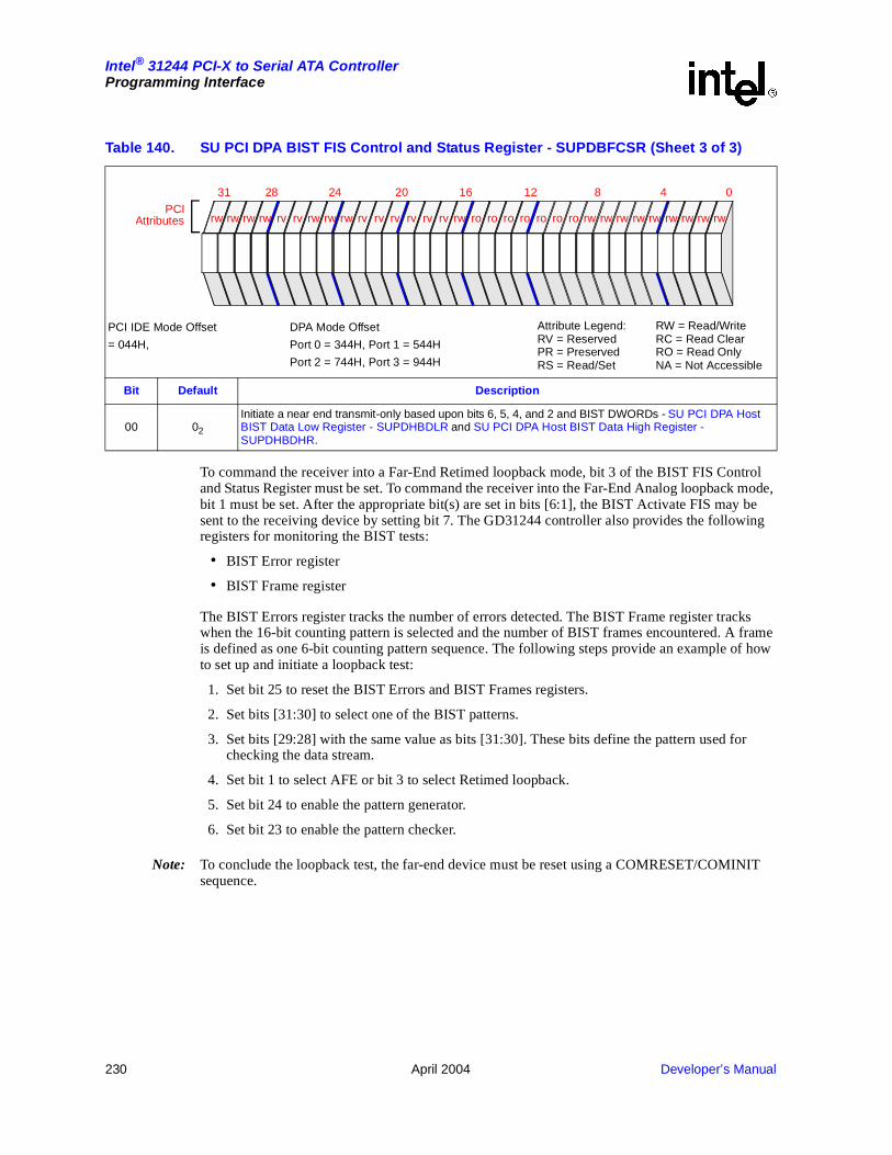
230 April 2004 Developer’s Manual
Intel® 31244 PCI-X to Serial ATA ControllerProgramming Interface
To command the receiver into a Far-End Retimed loopback mode, bit 3 of the BIST FIS Control and Status Register must be set. To command the receiver into the Far-End Analog loopback mode, bit 1 must be set. After the appropriate bit(s) are set in bits [6:1], the BIST Activate FIS may be sent to the receiving device by setting bit 7. The GD31244 controller also provides the following registers for monitoring the BIST tests:
• BIST Error register
• BIST Frame register
The BIST Errors register tracks the number of errors detected. The BIST Frame register tracks when the 16-bit counting pattern is selected and the number of BIST frames encountered. A frame is defined as one 6-bit counting pattern sequence. The following steps provide an example of how to set up and initiate a loopback test:
1. Set bit 25 to reset the BIST Errors and BIST Frames registers.
2. Set bits [31:30] to select one of the BIST patterns.
3. Set bits [29:28] with the same value as bits [31:30]. These bits define the pattern used for checking the data stream.
4. Set bit 1 to select AFE or bit 3 to select Retimed loopback.
5. Set bit 24 to enable the pattern generator.
6. Set bit 23 to enable the pattern checker.
Note: To conclude the loopback test, the far-end device must be reset using a COMRESET/COMINIT sequence.
00 02
Initiate a near end transmit-only based upon bits 6, 5, 4, and 2 and BIST DWORDs - SU PCI DPA Host BIST Data Low Register - SUPDHBDLR and SU PCI DPA Host BIST Data High Register - SUPDHBDHR.
Table 140. SU PCI DPA BIST FIS Control and Status Register - SUPDBFCSR (Sheet 3 of 3)
Bit Default Description
PCIAttributes
28 24 20 16 12 8 4 031
rw rw rw rw rv rv rw rw rw rv rv rv rv rv rv rw ro ro ro ro ro ro ro rw rw rw rw rw rw rw rw rw
Attribute Legend:RV = ReservedPR = PreservedRS = Read/Set
RW = Read/WriteRC = Read ClearRO = Read OnlyNA = Not Accessible
PCI IDE Mode Offset
= 044H,
DPA Mode Offset
Port 0 = 344H, Port 1 = 544H
Port 2 = 744H, Port 3 = 944H
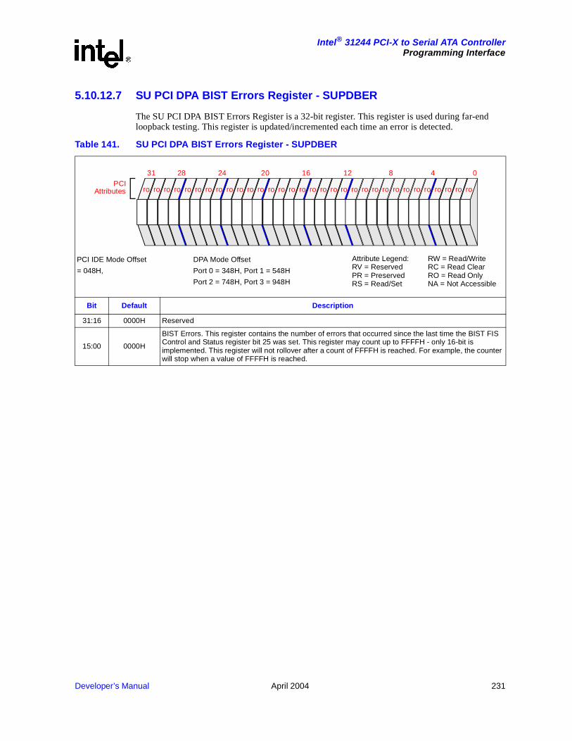
Developer’s Manual April 2004 231
Intel® 31244 PCI-X to Serial ATA ControllerProgramming Interface
5.10.12.7 SU PCI DPA BIST Errors Register - SUPDBER
The SU PCI DPA BIST Errors Register is a 32-bit register. This register is used during far-end loopback testing. This register is updated/incremented each time an error is detected.
Table 141. SU PCI DPA BIST Errors Register - SUPDBER
Bit Default Description
31:16 0000H Reserved
15:00 0000H
BIST Errors. This register contains the number of errors that occurred since the last time the BIST FIS Control and Status register bit 25 was set. This register may count up to FFFFH - only 16-bit is implemented. This register will not rollover after a count of FFFFH is reached. For example, the counter will stop when a value of FFFFH is reached.
PCIAttributes
28 24 20 16 12 8 4 031
ro ro ro ro ro ro ro ro ro ro ro ro ro ro ro ro ro ro ro ro ro ro ro ro ro ro ro ro ro ro ro ro
Attribute Legend:RV = ReservedPR = PreservedRS = Read/Set
RW = Read/WriteRC = Read ClearRO = Read OnlyNA = Not Accessible
PCI IDE Mode Offset
= 048H,
DPA Mode Offset
Port 0 = 348H, Port 1 = 548H
Port 2 = 748H, Port 3 = 948H
232 April 2004 Developer’s Manual
Intel® 31244 PCI-X to Serial ATA ControllerProgramming Interface
5.10.12.8 SU PCI DPA BIST Frames Register - SUPDBFR
The SU PCI DPA BIST Frames Register is a 32-bit register. This register is used during far-end loopback testing, and is only used for the counting pattern. Refer to bits [31:30] of the SU PCI DPA BIST FIS Control and Status Register - SUPDBFCSR for pattern selection.
Table 142. SU PCI DPA BIST Frames Register - SUPDBFR
Bit Default Description
31:00 0000_0000HBIST Frames. This register contains the number of BIST Frames that occurred since the last time the BIST FIS Control and Status register bit 25 was set. A BIST frame is 65536 DWORDs. Refer to Section 5.5, “Serial ATA BIST” on page 79 for a description of a BIST Frame.
PCIAttributes
28 24 20 16 12 8 4 031
ro ro ro ro ro ro ro ro ro ro ro ro ro ro ro ro ro ro ro ro ro ro ro ro ro ro ro ro ro ro ro ro
Attribute Legend:RV = ReservedPR = PreservedRS = Read/Set
RW = Read/WriteRC = Read ClearRO = Read OnlyNA = Not Accessible
PCI IDE Mode BAR5 Offset
= 04CH,
DPA Mode Offset
Port 0 = 34CH, Port 1 = 54CH
Port 2 = 74CH, Port 3 = 94CH

Developer’s Manual April 2004 233
Intel® 31244 PCI-X to Serial ATA ControllerProgramming Interface
5.10.12.9 SU PCI DPA Host BIST Data Low Register - SUPDHBDLR
The SU PCI DPA Host BIST Data Low Register is the first 32-bit parameter of the SATA BIST Activate Host-to-Device FIS. Refer to the Serial ATA Specification.
Table 143. SU PCI DPA Host BIST Data Low Register - SUPDHBDLR
Bit Default Description
31:00 0000_0000H This register contains the data transmitted as BIST FIS DWORD 1.
PCIAttributes
28 24 20 16 12 8 4 031
rw rw rw rw rw rw rw rw rw rw rw rw rw rw rw rw rw rw rw rw rw rw rw rw rw rw rw rw rw rw rw rw
Attribute Legend:RV = ReservedPR = PreservedRS = Read/Set
RW = Read/WriteRC = Read ClearRO = Read OnlyNA = Not Accessible
PCI IDE Mode Offset
= 050H,
DPA Mode Offset
Port 0 = 350H, Port 1 = 550H
Port 2 = 750H, Port 3 = 950H
234 April 2004 Developer’s Manual
Intel® 31244 PCI-X to Serial ATA ControllerProgramming Interface
5.10.12.10 SU PCI DPA Host BIST Data High Register - SUPDHBDHR
The SU PCI DPA Host BIST Data High Register is the second 32-bit parameter of the SATA Bist Activate Host-to-Device FIS. Refer to the Serial ATA Specification.
Table 144. SU PCI DPA Host BIST Data High Register - SUPDHBDHR
Bit Default Description
31:00 0000_0000H This register contains the data transmitted as BIST FIS DWORD 2.
PCIAttributes
28 24 20 16 12 8 4 031
rw rw rw rw rw rw rw rw rw rw rw rw rw rw rw rw rw rw rw rw rw rw rw rw rw rw rw rw rw rw rw rw
Attribute Legend:RV = ReservedPR = PreservedRS = Read/Set
RW = Read/WriteRC = Read ClearRO = Read OnlyNA = Not Accessible
PCI IDE Mode Offset
= 054H,
DPA Mode Offset
Port 0 = 354H, Port 1 = 554H
Port 2 = 754H, Port 3 = 954H
Developer’s Manual April 2004 235
Intel® 31244 PCI-X to Serial ATA ControllerProgramming Interface
5.10.12.11 SU PCI DPA Device BIST Data Low Register - SUPDDBDLR
The SU PCI DPA Device BIST Data Low Register is the first 32-bit parameter of the SATA Bist Activate Device-to-Host FIS. Refer to the Serial ATA Specification.
Table 145. SU PCI DPA Device BIST Data Low Register - SUPDDBDLR
Bit Default Description
31:00 0000_0000H This register contains the data transmitted as BIST FIS DWORD 1.
PCIAttributes
28 24 20 16 12 8 4 031
ro ro ro ro ro ro ro ro ro ro ro ro ro ro ro ro ro ro ro ro ro ro ro ro ro ro ro ro ro ro ro ro
Attribute Legend:RV = ReservedPR = PreservedRS = Read/Set
RW = Read/WriteRC = Read ClearRO = Read OnlyNA = Not Accessible
PCI IDE Mode Offset
= 058H,
DPA Mode Offset
Port 0 = 358H, Port 1 = 558H
Port 2 = 758H, Port 3 = 958H

236 April 2004 Developer’s Manual
Intel® 31244 PCI-X to Serial ATA ControllerProgramming Interface
5.10.12.12 SU PCI DPA Device BIST Data High Register - SUPDDBDHR
The SU PCI DPA Device BIST Data High Register is the second 32-bit parameter of the SATA Bist Activate Device-to-Host FIS. Refer to the Serial ATA Specification.
Table 146. SU PCI DPA Device BIST Data High Register - SUPDDBDHR
Bit Default Description
31:00 0000_0000H This register contains the data transmitted as BIST FIS DWORD 2.
PCIAttributes
28 24 20 16 12 8 4 031
ro ro ro ro ro ro ro ro ro ro ro ro ro ro ro ro ro ro ro ro ro ro ro ro ro ro ro ro ro ro ro ro
Attribute Legend:RV = ReservedPR = PreservedRS = Read/Set
RW = Read/WriteRC = Read ClearRO = Read OnlyNA = Not Accessible
PCI IDE Mode Offset
= 05CH,
DPA Mode Offset
Port 0 = 35CH, Port 1 = 55CH
Port 2 = 75CH, Port 3 = 95CH

Developer’s Manual April 2004 237
Intel® 31244 PCI-X to Serial ATA ControllerProgramming Interface
5.10.12.13 SU PCI DPA Queuing Table Base Address Register Low - SUPDQTBARL
This register contains the lower values added to the DMA buffer identifier to determine the base address of the PRD.
Table 147. SU PCI DPA Device BIST Data High Register - SUPDDBDHR
Bit Default Description
31:00 0000_0000H Value used by the DMA engine to add to the DMA Buffer identifier to get the base address of the PRD, bits 31:0.
PCIAttributes
28 24 20 16 12 8 4 031
rw rw rw rw rw rw rw rw rw rw rw rw rw rw rw rw rw rw rw rw rw rw rw rw rw rw rw rw rw rw ro rw
Attribute Legend:RV = ReservedPR = PreservedRS = Read/Set
RW = Read/WriteRC = Read ClearRO = Read OnlyNA = Not Accessible
PCI IDE Mode Offset
= 060H,
DPA Mode Offset
Port 0 = 360H, Port 1 = 560CH
Port 2 = 760H, Port 3 = 960H
238 April 2004 Developer’s Manual
Intel® 31244 PCI-X to Serial ATA ControllerProgramming Interface
5.10.12.14 SU PCI DPA Queuing Table Base Address Register High - SUPDQTBARH
This register contains the lower values added to the DMA buffer identifier to determine the base address of the PRD.
Table 148. SU PCI DPA Device BIST Data High Register - SUPDDBDHR
Bit Default Description
31:00 0000_0000H Value used by the DMA engine to add to the DMA Buffer identifier to get the base address of the PRD, bits 63:32.
PCIAttributes
28 24 20 16 12 8 4 031
rw rw rw rw rw rw rw rw rw rw rw rw rw rw rw rw rw rw rw rw rw rw rw rw rw rw rw rw rw rw ro rw
Attribute Legend:RV = ReservedPR = PreservedRS = Read/Set
RW = Read/WriteRC = Read ClearRO = Read OnlyNA = Not Accessible
PCI IDE Mode Offset
= 064H,
DPA Mode Offset
Port 0 = 364H, Port 1 = 564CH
Port 2 = 764H, Port 3 = 964H
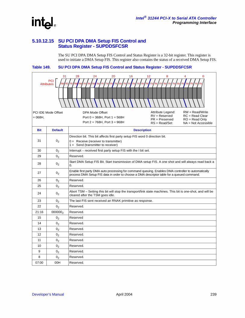
Developer’s Manual April 2004 239
Intel® 31244 PCI-X to Serial ATA ControllerProgramming Interface
5.10.12.15 SU PCI DPA DMA Setup FIS Control and Status Register - SUPDDSFCSR
The SU PCI DPA DMA Setup FIS Control and Status Register is a 32-bit register. This register is used to initiate a DMA Setup FIS. This register also contains the status of a received DMA Setup FIS.
Table 149. SU PCI DPA DMA Setup FIS Control and Status Register - SUPDDSFCSR
Bit Default Description
31 02
Direction bit. This bit affects first party setup FIS word 0 direction bit.
0 = Receive (receiver to transmitter)1 = Send (transmitter to receiver)
30 02 Interrupt – received first party setup FIS with the I bit set.
29 02 Reserved.
28 02Start DMA Setup FIS Bit. Start transmission of DMA setup FIS. A one shot and will always read back a 0.
27 02Enable first party DMA auto processing for command queuing. Enables DMA controller to automatically process DMA Setup FIS data in order to choose a DMA descriptor table for a queued command.
26 02 Reserved.
25 02 Reserved.
24 02Abort TSM – Setting this bit will stop the transport/link state machines. This bit is one-shot, and will be cleared after the TSM goes idle.
23 02 The last FIS sent received an RNAK primitive as response.
22 02 Reserved.
21:16 0000002 Reserved.
15 02 Reserved
14 02 Reserved.
13 02 Reserved.
12 02 Reserved.
11 02 Reserved.
10 02 Reserved.
9 02 Reserved.
8 02 Reserved.
07:00 00H Reserved.
PCIAttributes
28 24 20 16 12 8 4 031
rw ro rv rw rw rv rv rw rv rv rv rv rv rv rv rv rv rv rv rv rv rv rv rv rv rv rv rv rv rv rv rv
Attribute Legend:RV = ReservedPR = PreservedRS = Read/Set
RW = Read/WriteRC = Read ClearRO = Read OnlyNA = Not Accessible
PCI IDE Mode Offset
= 068H,
DPA Mode Offset
Port 0 = 368H, Port 1 = 568H
Port 2 = 768H, Port 3 = 968H

240 April 2004 Developer’s Manual
Intel® 31244 PCI-X to Serial ATA ControllerProgramming Interface
5.10.12.16 SU PCI DPA Host DMA Buffer Identifier Low Register - SUPDHDBILR
The SU PCI DPA Host DMA Buffer Identifier Low Register is the first DWORD parameter of the SATA DMA Setup Host-to-Device FIS. Refer to the Serial ATA Specification.
Table 150. SU PCI DPA Host DMA Buffer Identifier Low Register - SUPDHDBILR
Bit Default Description
31:00 0000_0000H Buffer Identifier Low - This is the lower DWORD of a 64-bit buffer identifier, which may be used to identify a DMA buffer region in host memory.
PCIAttributes
28 24 20 16 12 8 4 031
rw rw rw rw rw rw rw rw rw rw rw rw rw rw rw rw rw rw rw rw rw rw rw rw rw rw rw rw rw rw rw rw
Attribute Legend:RV = ReservedPR = PreservedRS = Read/Set
RW = Read/WriteRC = Read ClearRO = Read OnlyNA = Not Accessible
PCI IDE Mode Offset
= 06CH,
DPA Mode Offset
Port 0 = 36CH, Port 1 = 56CH
Port 2 = 76CH, Port 3 = 96CH

Developer’s Manual April 2004 241
Intel® 31244 PCI-X to Serial ATA ControllerProgramming Interface
5.10.12.17 SU PCI DPA Host DMA Buffer Identifier High Register - SUPDHDBIHR
The SU PCI DPA Host DMA Buffer Identifier High Register is the second DWORD parameter of the SATA DMA Setup Host-to-Device FIS. Refer to the Serial ATA Specification.
Table 151. SU PCI DPA Host DMA Buffer Identifier High Register - SUPDHDBIHR
Bit Default Description
31:00 0000_0000H Buffer Identifier High - This is the upper DWORD of a 64-bit buffer identifier, which may be used to identify a DMA buffer region in host memory.
PCIAttributes
28 24 20 16 12 8 4 031
rw rw rw rw rw rw rw rw rw rw rw rw rw rw rw rw rw rw rw rw rw rw rw rw rw rw rw rw rw rw rw rw
Attribute Legend:RV = ReservedPR = PreservedRS = Read/Set
RW = Read/WriteRC = Read ClearRO = Read OnlyNA = Not Accessible
PCI IDE Mode Offset
= 070H,
DPA Mode Offset
Port 0 = 370H, Port 1 = 570H
Port 2 = 770H, Port 3 = 970H

242 April 2004 Developer’s Manual
Intel® 31244 PCI-X to Serial ATA ControllerProgramming Interface
5.10.12.18 SU PCI DPA Host Reserved DWORD Register 0 - SUPDHRDR0
The SU PCI DPA Host Reserved Register 0 is the third DWORD parameter of the SATA DMA Setup Host-to-Device FIS. Refer to the Serial ATA Specification.
Table 152. SU PCI DPA Host Reserved DWORD Register 0 - SUPDHRDR 0
Bit Default Description
31:00 0000_0000H Reserved DWORD in the SATA DMA Setup Host-to-Device FIS.
PCIAttributes
28 24 20 16 12 8 4 031
rw rw rw rw rw rw rw rw rw rw rw rw rw rw rw rw rw rw rw rw rw rw rw rw rw rw rw rw rw rw rw rw
Attribute Legend:RV = ReservedPR = PreservedRS = Read/Set
RW = Read/WriteRC = Read ClearRO = Read OnlyNA = Not Accessible
PCI IDE Mode Offset
= 074H,
DPA Mode Offset
Port 0 = 374H, Port 1 = 574H
Port 2 = 774H, Port 3 = 974H

Developer’s Manual April 2004 243
Intel® 31244 PCI-X to Serial ATA ControllerProgramming Interface
5.10.12.19 SU PCI DPA Host DMA Buffer Offset Register - SUPDHDBOR
The SU PCI DPA Host DMA Buffer Offset Register is the fourth DWORD parameter of the SATA DMA Setup Host-to-Device FIS. Refer to the Serial ATA Specification.
Table 153. SU PCI DPA Host DMA Buffer Offset Register - SUPDHDBOR
Bit Default Description
31:00 0000_0000H Buffer Offset - This is the byte offset into the DMA buffer region.
PCIAttributes
28 24 20 16 12 8 4 031
rw rw rw rw rw rw rw rw rw rw rw rw rw rw rw rw rw rw rw rw rw rw rw rw rw rw rw rw rw rw rw rw
Attribute Legend:RV = ReservedPR = PreservedRS = Read/Set
RW = Read/WriteRC = Read ClearRO = Read OnlyNA = Not Accessible
PCI IDE Mode Offset
= 078H,
DPA Mode Offset
Port 0 = 378H, Port 1 = 578H
Port 2 = 778H, Port 3 = 978H

244 April 2004 Developer’s Manual
Intel® 31244 PCI-X to Serial ATA ControllerProgramming Interface
5.10.12.20 SU PCI DPA Host DMA Transfer Count Register - SUPDHDTCR
The SU PCI DPA Host DMA Transfer Count Register is the fifth DWORD parameter of the SATA DMA Setup Host-to-Device FIS. Refer to the Serial ATA Specification.
Table 154. SU PCI DPA Host DMA Transfer Count Register - SUPDHDTCR
Bit Default Description
31:00 0000_0000H Transfer Count - This is the number of bytes that will be read or written by the device.
PCIAttributes
28 24 20 16 12 8 4 031
rw rw rw rw rw rw rw rw rw rw rw rw rw rw rw rw rw rw rw rw rw rw rw rw rw rw rw rw rw rw rw rw
Attribute Legend:RV = ReservedPR = PreservedRS = Read/Set
RW = Read/WriteRC = Read ClearRO = Read OnlyNA = Not Accessible
PCI IDE Mode Offset
= 07CH,
DPA Mode Offset
Port 0 = 37CH, Port 1 = 57CH
Port 2 = 77CH, Port 3 = 97CH

Developer’s Manual April 2004 245
Intel® 31244 PCI-X to Serial ATA ControllerProgramming Interface
5.10.12.21 SU PCI DPA Host Reserved DWORD Register 1- SUPDHRDR1
The SU PCI DPA Host Reserved Register 1 is the sixth DWORD parameter of the SATA DMA Setup Host-to-Device FIS. Refer to the Serial ATA Specification.
Table 155. SU PCI DPA Host Reserved DWORD Register 1- SUPDHRDR 1
Bit Default Description
31:00 0000_0000H Reserved DWORD in the SATA DMA Setup Host-to-Device FIS.
PCIAttributes
28 24 20 16 12 8 4 031
rw rw rw rw rw rw rw rw rw rw rw rw rw rw rw rw rw rw rw rw rw rw rw rw rw rw rw rw rw rw rw rw
Attribute Legend:RV = ReservedPR = PreservedRS = Read/Set
RW = Read/WriteRC = Read ClearRO = Read OnlyNA = Not Accessible
PCI IDE Mode Offset
= 080H,
DPA Mode Offset
Port 0 = 380H, Port 1 = 580H
Port 2 = 780H, Port 3 = 980H

246 April 2004 Developer’s Manual
Intel® 31244 PCI-X to Serial ATA ControllerProgramming Interface
5.10.12.22 SU PCI DPA Device DMA Buffer Identifier Low Register - SUPDDDBILR
The SU PCI DPA Device DMA Buffer Identifier Low Register is the first DWORD parameter of the SATA DMA Setup Device-to-Host FIS. Refer to the Serial ATA Specification.
Table 156. SU PCI DPA Device DMA Buffer Identifier Low Register - SUPDDDBILR
Bit Default Description
31:00 0000_0000H Buffer Identifier Low - This is the lower DWORD of a 64-bit buffer identifier, which may be used to identify a DMA buffer region of the First Party Setup FIS received from a device.
PCIAttributes
28 24 20 16 12 8 4 031
ro ro ro ro ro ro ro ro ro ro ro ro ro ro ro ro ro ro ro ro ro ro ro ro ro ro ro ro ro ro ro ro
Attribute Legend:RV = ReservedPR = PreservedRS = Read/Set
RW = Read/WriteRC = Read ClearRO = Read OnlyNA = Not Accessible
PCI IDE Mode Offset
= 084H,
DPA Mode Offset
Port 0 = 384H, Port 1 = 584H
Port 2 = 784H, Port 3 = 984H

Developer’s Manual April 2004 247
Intel® 31244 PCI-X to Serial ATA ControllerProgramming Interface
5.10.12.23 SU PCI DPA Device DMA Buffer Identifier High Register - SUPDDDBIHR
The SU PCI DPA Device DMA Buffer Identifier High Register is the second DWORD parameter of the SATA DMA Setup Device-to-Host FIS. Refer to the Serial ATA Specification.
Table 157. SU PCI DPA Device DMA Buffer Identifier High Register - SUPDDDBIHR
Bit Default Description
31:00 0000_0000H Buffer Identifier High - This is the upper 32 bits of the DMA Buffer Identifier field of the First Party Setup FIS received from a device.
PCIAttributes
28 24 20 16 12 8 4 031
ro ro ro ro ro ro ro ro ro ro ro ro ro ro ro ro ro ro ro ro ro ro ro ro ro ro ro ro ro ro ro ro
Attribute Legend:RV = ReservedPR = PreservedRS = Read/Set
RW = Read/WriteRC = Read ClearRO = Read OnlyNA = Not Accessible
PCI IDE Mode Offset
= 088H,
DPA Mode Offset
Port 0 = 388H, Port 1 = 588H
Port 2 = 788H, Port 3 = 988H

248 April 2004 Developer’s Manual
Intel® 31244 PCI-X to Serial ATA ControllerProgramming Interface
5.10.12.24 SU PCI DPA Host Reserved DWORD Register 0 - SUPDHRDR0
The SU PCI DPA Received Host Reserved Register 0 is the third DWORD parameter of the SATA DMA Setup Host-to-Device FIS. Refer to the Serial ATA Specification.
Table 158. SU PCI DPA Device Reserved DWORD Register 0 - SUPDDRDR0
Bit Default Description
31:00 0000_0000H Reserved DWORD in the SATA DMA Setup Device-to-Host FIS.
PCIAttributes
28 24 20 16 12 8 4 031
ro ro ro ro ro ro ro ro ro ro ro ro ro ro ro ro ro ro ro ro ro ro ro ro ro ro ro ro ro ro ro ro
Attribute Legend:RV = ReservedPR = PreservedRS = Read/Set
RW = Read/WriteRC = Read ClearRO = Read OnlyNA = Not Accessible
PCI IDE Mode Offset
= 08CH,
DPA Mode Offset
Port 0 = 38CH, Port 1 = 58CH
Port 2 = 78CH, Port 3 = 98CH
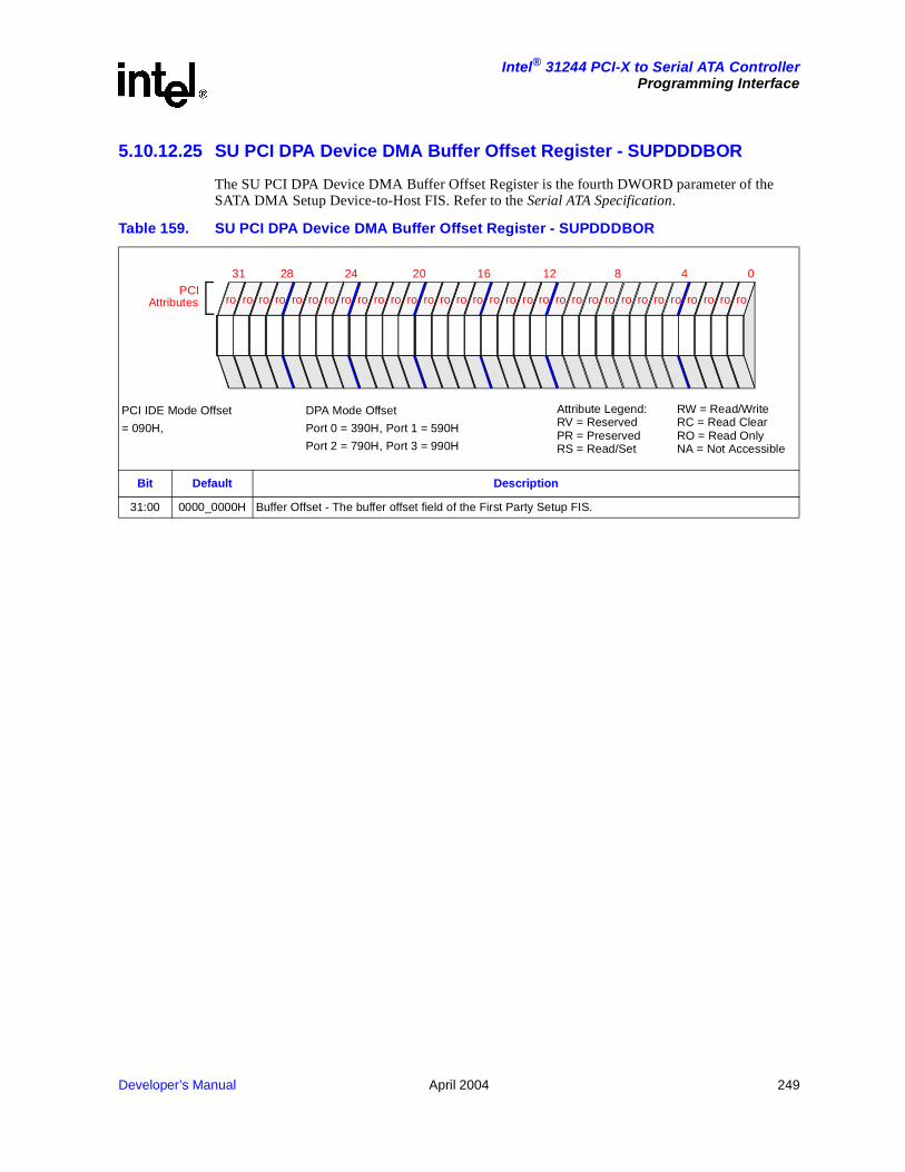
Developer’s Manual April 2004 249
Intel® 31244 PCI-X to Serial ATA ControllerProgramming Interface
5.10.12.25 SU PCI DPA Device DMA Buffer Offset Register - SUPDDDBOR
The SU PCI DPA Device DMA Buffer Offset Register is the fourth DWORD parameter of the SATA DMA Setup Device-to-Host FIS. Refer to the Serial ATA Specification.
Table 159. SU PCI DPA Device DMA Buffer Offset Register - SUPDDDBOR
Bit Default Description
31:00 0000_0000H Buffer Offset - The buffer offset field of the First Party Setup FIS.
PCIAttributes
28 24 20 16 12 8 4 031
ro ro ro ro ro ro ro ro ro ro ro ro ro ro ro ro ro ro ro ro ro ro ro ro ro ro ro ro ro ro ro ro
Attribute Legend:RV = ReservedPR = PreservedRS = Read/Set
RW = Read/WriteRC = Read ClearRO = Read OnlyNA = Not Accessible
PCI IDE Mode Offset
= 090H,
DPA Mode Offset
Port 0 = 390H, Port 1 = 590H
Port 2 = 790H, Port 3 = 990H

250 April 2004 Developer’s Manual
Intel® 31244 PCI-X to Serial ATA ControllerProgramming Interface
5.10.12.26 SU PCI DPA Device DMA Transfer Count Register - SUPDDDTCR
The SU PCI DPA Device DMA Transfer Count Register is the fifth DWORD parameter of the SATA DMA Setup Device-to-Host FIS. Refer to the Serial ATA Specification.
Table 160. SU PCI DPA Device DMA Transfer Count Register - SUPDDTCR
Bit Default Description
31:00 0000_0000H Transfer Count - The transfer Count field of the First Party Setup FIS.
PCIAttributes
28 24 20 16 12 8 4 031
ro ro ro ro ro ro ro ro ro ro ro ro ro ro ro ro ro ro ro ro ro ro ro ro ro ro ro ro ro ro ro ro
Attribute Legend:RV = ReservedPR = PreservedRS = Read/Set
RW = Read/WriteRC = Read ClearRO = Read OnlyNA = Not Accessible
DPA Mode Offset
Port 0 = 394H, Port 1 = 594H
Port 2 = 794H, Port 3 = 994H
PCI IDE Mode Offset
= 094H,

Developer’s Manual April 2004 251
Intel® 31244 PCI-X to Serial ATA ControllerProgramming Interface
5.10.12.27 SU PCI DPA Device Reserved DWORD Register 1 - SUPDDRDR1
The SU PCI DPA Device Reserved Register 1 is the sixth DWORD parameter of the SATA DMA Setup Host-to-Device FIS. Refer to the Serial ATA Specification.
Table 161. SU PCI DPA Device Reserved DWORD Register 1 - SUPDDRDR1
Bit Default Description
31:00 0000_0000H Reserved DWORD in the SATA DMA Setup Device-to-Host FIS.
PCIAttributes
28 24 20 16 12 8 4 031
ro ro ro ro ro ro ro ro ro ro ro ro ro ro ro ro ro ro ro ro ro ro ro ro ro ro ro ro ro ro ro ro
Attribute Legend:RV = ReservedPR = PreservedRS = Read/Set
RW = Read/WriteRC = Read ClearRO = Read OnlyNA = Not Accessible
PCI IDE Mode Offset
= 098H,
DPA Mode Offset
Port 0 = 398H, Port 1 = 598H
Port 2 = 798H, Port 3 = 998H

252 April 2004 Developer’s Manual
Intel® 31244 PCI-X to Serial ATA ControllerProgramming Interface
This Page Left Intentionally Blank