INTEGRATION OF ACTIVE MATERIALS WITH SILICON
7
INTEGRATION OF ACTIVE MATERIALS WITH SILICON MICROMACHINING : APPLICATIONS TO OPTICAL MEMS Jean-Philippe GOUY, Yasuhiko ARAKAWA and Hiroyuki FUJITA LIMMS/CNRS-IIS, RCAST and CIRMM, Institute of Industrial Science The University of Tokyo 4-6-1 Komaba, Meguro-ku, 153-8505 Tokyo, Japan Tel : 81 3 5452 6036, Fax : 81 3 5452 6088 Email : [email protected] ABSTRACT Most of the MOEMS including optical switches and micro optical benches are developed on silicon. As for the MEMS, the main reason is that silicon has consistently been the material of choice for the microelectronics industry, due to a mature processing technology which offers the possibility to integrate MEMS devices with Integrated Circuits in a low cost batch fabrication process. However, since the beginning of Optoelectronic, silicon has been suffering from its poor efficiency to emit light because of its indirect band gap. Optical active devices can be integrated on silicon by combining specific active materials in order to keep the main advantage of silicon micromachining for MOEMS applications. This paper illustrates this purpose through one project developed in the frame of the LIMMS, joint laboratory between France and Japan. This project deals with optical active devices for which silicon micromachining technology has been employed to fabricate an organic semiconductors based light emitted diode on silicon substrate. Keywords: MOEMS, silicon micromachnining, organic semiconductor, LED 1. INTRODUCTION Optical MEMS so called MOEMS are usually made by the integration of both optical, electrical and mechanical components in one microsystem and therefore are well known to be the key devices of high-performance systems in many applications as telecommunication, automotive… 1 As silicon has been suffering since the beginning of Optoelectronic from its poor efficiency to emit light because of its indirect band gap, most of the MOEMS are based, as for optoelectronic devices, on III-V material when the emission of light is required. The interest to combine both III-V and silicon technology remains very strong, and many works are developed in this direction. An other alternative to integrate emitting devices on silicon is proposed in this work with the integration of organic semiconductor based emitting devices on silicon substrate. During the last decade, organic semiconductors have attracted increasing research interest from both academia and industry. Investigation of material properties, device structures and characteristics show that electronic and photonic devices can be successfully prepared from organic compounds. The most difficult operation is the fabrication of devices with good reliability. Among the different techniques developed for the deposition of polymeric films, Organic Molecular Beam Deposition (OMBD) technology allows the subsequent growth of thin solid films and was used for example to deposit organic semiconductor on III-V material for microwave application 2,3 . For optical application with the fabrication of Organic Light Emitting Diode (OLED), most of the reported devices propose the deposition of organic semiconductor on glass, which is transparent at the working wavelength, usually in the visible range. A silicon-based organic light emitting diode has been reported 4 , for operation at a wavelength of - cavity surface-emitting laser was demonstrated around 500nm with optically pumped structures on quartz 5 and one of the first organic semiconductor-based microcavities on silicon has been realised by a French Team from Lyon, LEOM 6 where Massenelli and his co-worker deposited on silicon substrate all the active layers for a device which emits light at 515nm under optical pumping.
Transcript of INTEGRATION OF ACTIVE MATERIALS WITH SILICON

INTEGRATION OF ACTIVE MATERIALS WITH SILICON MICROMACHINING : APPLICATIONS TO OPTICAL MEMS
Jean-Philippe GOUY, Yasuhiko ARAKAWA and Hiroyuki FUJITA
LIMMS/CNRS-IIS, RCAST and CIRMM, Institute of Industrial Science
The University of Tokyo 4-6-1 Komaba, Meguro-ku, 153-8505 Tokyo, Japan
Tel : 81 3 5452 6036, Fax : 81 3 5452 6088 Email : [email protected]
ABSTRACT Most of the MOEMS including optical switches and micro optical benches are developed on silicon. As for the MEMS, the main reason is that silicon has consistently been the material of choice for the microelectronics industry, due to a mature processing technology which offers the possibility to integrate MEMS devices with Integrated Circuits in a low cost batch fabrication process. However, since the beginning of Optoelectronic, silicon has been suffering from its poor efficiency to emit light because of its indirect band gap. Optical active devices can be integrated on silicon by combining specific active materials in order to keep the main advantage of silicon micromachining for MOEMS applications. This paper illustrates this purpose through one project developed in the frame of the LIMMS, joint laboratory between France and Japan. This project deals with optical active devices for which silicon micromachining technology has been employed to fabricate an organic semiconductors based light emitted diode on silicon substrate. Keywords: MOEMS, silicon micromachnining, organic semiconductor, LED
1. INTRODUCTION Optical MEMS so called MOEMS are usually made by the integration of both optical, electrical and mechanical components in one microsystem and therefore are well known to be the key devices of high-performance systems in many applications as telecommunication, automotive…1 As silicon has been suffering since the beginning of Optoelectronic from its poor efficiency to emit light because of its indirect band gap, most of the MOEMS are based, as for optoelectronic devices, on III-V material when the emission of light is required. The interest to combine both III-V and silicon technology remains very strong, and many works are developed in this direction. An other alternative to integrate emitting devices on silicon is proposed in this work with the integration of organic semiconductor based emitting devices on silicon substrate. During the last decade, organic semiconductors have attracted increasing research interest from both academia and industry. Investigation of material properties, device structures and characteristics show that electronic and photonic devices can be successfully prepared from organic compounds. The most difficult operation is the fabrication of devices with good reliability. Among the different techniques developed for the deposition of polymeric films, Organic Molecular Beam Deposition (OMBD) technology allows the subsequent growth of thin solid films and was used for example to deposit organic semiconductor on III-V material for microwave application 2,3. For optical application with the fabrication of Organic Light Emitting Diode (OLED), most of the reported devices propose the deposition of organic semiconductor on glass, which is transparent at the working wavelength, usually in the visible range. A silicon-based organic light emitting diode has been reported 4, for operation at a wavelength of ����P IRU ZKLFK VLOLFRQ LV D WUDQVSDUHQW PDWHULDO� /DVLQJ DFWLRQ LQ RUJDQLF YHUWLFDO-cavity surface-emitting laser was demonstrated around 500nm with optically pumped structures on quartz 5 and one of the first organic semiconductor-based microcavities on silicon has been realised by a French Team from Lyon, LEOM 6 where Massenelli and his co-worker deposited on silicon substrate all the active layers for a device which emits light at 515nm under optical pumping.
As organic semiconductors are very attractive for their broad emission spectrum according to their chemical structures 7 the possibility to deposit any kind of OLED on silicon seems to be very attractive for both the integration of the electronic and the use of MEMS capability.
2. DEPOSITION TECHNIQUE
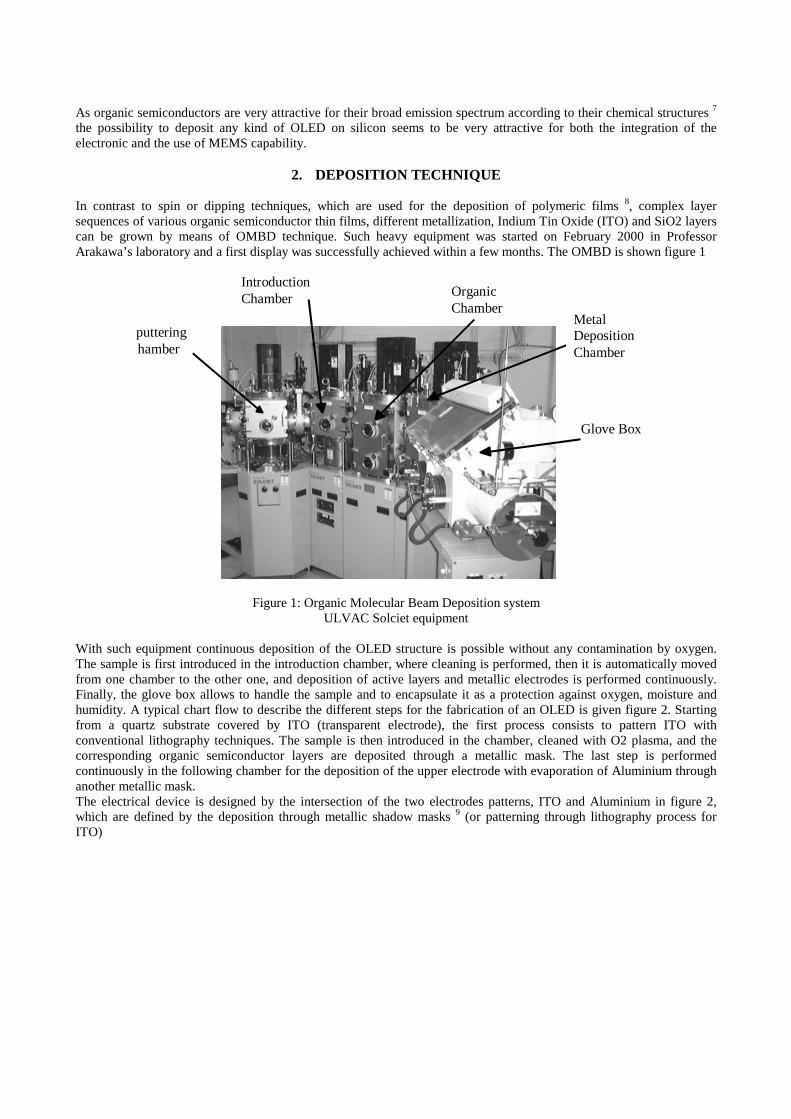
In contrast to spin or dipping techniques, which are used for the deposition of polymeric films 8, complex layer sequences of various organic semiconductor thin films, different metallization, Indium Tin Oxide (ITO) and SiO2 layers can be grown by means of OMBD technique. Such heavy equipment was started on February 2000 in Professor Arakawa’s laboratory and a first display was successfully achieved within a few months. The OMBD is shown figure 1
IntroductionChamber
putteringhamber
OrganicChamber
Glove Box
MetalDepositionChamber
Figure 1: Organic Molecular Beam Deposition system ULVAC Solciet equipment
With such equipment continuous deposition of the OLED structure is possible without any contamination by oxygen. The sample is first introduced in the introduction chamber, where cleaning is performed, then it is automatically moved from one chamber to the other one, and deposition of active layers and metallic electrodes is performed continuously. Finally, the glove box allows to handle the sample and to encapsulate it as a protection against oxygen, moisture and humidity. A typical chart flow to describe the different steps for the fabrication of an OLED is given figure 2. Starting from a quartz substrate covered by ITO (transparent electrode), the first process consists to pattern ITO with conventional lithography techniques. The sample is then introduced in the chamber, cleaned with O2 plasma, and the corresponding organic semiconductor layers are deposited through a metallic mask. The last step is performed continuously in the following chamber for the deposition of the upper electrode with evaporation of Aluminium through another metallic mask. The electrical device is designed by the intersection of the two electrodes patterns, ITO and Aluminium in figure 2, which are defined by the deposition through metallic shadow masks 9 (or patterning through lithography process for ITO)

ITO Pattern Organic MaterialDeposition
Al Deposition
Deposition through masksor
Lithography and etching
Depositionthrough
Metallic Masks
CurrentInjection
EmissionAt
0.5 µm
Figure 2: typical steps for OLED fabrication on quartz.
In order two improve the design of OLED, deposition through Silicon shadow masks is proposed in this work. Based on the use of Deep Reactive Ion Etching for the fabrication of these masks, the two main advantages offered by silicon micromachining are:
- To define very narrow patterns by the use of lithography process - To insure an accurate alignment between different shadow masks by the use of mechanical alignment
designed also at the same lithography process 10 However, the use of silicon shadow masks requires mechanical alignment system on both the shadow mask and the device on which the deposition is performed. A silicon microstructure for the OLED is designed to integrate this mechanical alignment set-up.
3. PRINCIPE
The proposed silicon microstructure with the integration scheme of the OLED is given figure 3. As Silicon absorbs light XQWLO ����P� WKH PLFURVWUXFWXUH LV EDVed on a transparent membrane which has to be design thank to mechanical and process considerations. For the electrical aspect, the main interest of silicon micromachining with the well known anisotropic etching of silicon allows to realise the proposed shape in order to avoid any discontinuity in the electrical circuits for both ITO and Al pads.
AlOMITOSi waferSiO2/ SiN…
emission
Figure 3 : Proposed microstructure for OLED deposition

Micromachined micro-holes
for mechanical
Shape ofmicro-recess
Figure 4 : integration scheme of mechanical alignment setup on the microstructure
1
2Silicon Micromachined Pinfor Mechanical Alignment
Figure 5 : mechanical assembly scheme of the microstructure (right) on the shadow mask (top left) with micromachined silicon pin (bottom left)
The mechanical alignement setup is given figure 4. Micromachined microhole are performed with Deep Reactive Ion Etching (ICP-RIE) as the first technological step for the fabrication of the microstruture. The same microholes are integrated on the silicon shadow masks, micromachined in a whole silicon wafer, and alignment is insure through micromachined 4 silicon pins which are inserted with a tweezer (figure 5). The main interests are :
- to change easily masks in the glove boxe, in nitrogene environment - to keep a very good alignment between the following process, thank to the alignment setup - to pattern a device structure without any conventional lithography process

Moreover, thank to the good compatibility between silicon micromachining and organic semiconductor deposition, in the way that deposition is performed after all the silicon process in a dry environment, the proposed solution permit to design any device with the integration of complex Micro Electrical Mechnical System as for instance, tunable Fabry Perot filter, which may be integrated with white ligth OLED, already reported 11
4. EXPERIMENTS AND RESULTS
The structure of the fabricated OLED is given in table 1. These conditions were optimized in Professor Arakawa’s laboratory.
Process Conditions Thickness / time 1 ITO sputtering RF power 400 W - room temperature - P:
0.27 Pa 200 nm / 10 mn
2 Cleaning : O2 plasma O2 : 56sccm, P : 1 Pa, Rf : 100W 1mn 3 a-NPD deposition T : 255°C, P : 3 10-5 Pa,
Rate : 0.1 nm/mn 60 nm
4 Alq deposition T : 275°C, P : 3 10-5 Pa, Rate : 0.1 nm/mn
60 nm
5 LiF deposition T : 600°C, P : 2 10-4 Pa, Rate : 0.01 nm/mn
0.5 nm
6 Al deposition P : 2 10-4 Pa, Rate : 0.2 nm/mn 120 nm
Table 1 : OLED deposition process
Micromachined micro-holesfor mechanical alignment
Shape of the Silicon Microstructure withdeposited material
Deposition ThroughShadow Mask
or
or
Relative Alignment
Micromachined micro-holesfor deposition Shape
ITO
OMAl
Figure 6 : depostion scheme through 3 different silicon shadow masks
The three deposition process, ITO, Organic Material (a-NPD and Alq) and Al (with LiF to improve carrier transfer) are performed through 3 differents silicon shadow masks according to the proposed scheme given figure 6 For the fabrication of the silicon microstructure, and silicon shadow masks itself, almost 2 weeks are necessary to perform Al deposition, ICP-RIE, oxydation, LPCVD and anisotropic etching with the corresponding lithography steps. The deposition of the OLED structure is performed in several hours, mainly due to the pumping time between the different operations. A first result is given figure 7 with a large view of the structure which shows a quite good alignment of each deposited layer. For this first realisation, a typical electrical characteristic of a diode was obtained (figure 8) with the emission of green light during a few second

ITO
Al
OM
Figure 7: SEM and optical microscope top view of the device
0.0E+00
2.0E-07
4.0E-07
6.0E-07
8.0E-07
1.0E-06
1.2E-06
1.4E-06
0 2 4 6 8 10
Voltage (V)
Cur
rent
(A
)
Figure 8: experimental electrical characteristic .
5. CONCLUSION This work reported a new method for the fabrication of Organic Light Emitting Diode on Silicon microstructure with the use of silicon micromachined shadow masks. The proposed concept should be useful for the integration of any kind of OLED deposited with Organic Molecular Beam Deposition technique, with silicon based MEMS and /or Integrated circuit. A first realization was reported which shows the capability to deposit and pattern OLED structure without any conventional lithography process. The improvement of the proposed technique is going on, with the design of new silicon shadow masks, particularly to control the sputtering deposition through micromachined shadow mask, which is to our knowledge, proposed for the first time in this work. The second aspect is the design and fabrication of silicon microstructures to perform transparent membranes as large as possible, in order to control the injection of current in a homogenous organic semiconductor layer.

ACKNOWLEDGMENT
This project is performed in the frame of LIMMS, Laboratory for Integrated Micro Mechatronic Systems, a joint laboratory between the CNRS-France and the University of Tokyo-Japan. It is supported by the CNRS, the Monbukagakusho (Japanese Ministry for Education, Science and Technology) and the JSPS. The authors would like to thank all the Japanese and French members of the laboratories involved in this project, particularly Dr Kitamura who developed and performed all the organic semiconductor deposition. The fabrication of the mask for conventional lithography was realized in the frame and with the technical support of the VDEC, VLSI Design and Educational Centre of the University of Tokyo.
REFERENCES 1. H. Fujita, H. Toshiyoshi, "Optical MEMS", IEICE Trans. on Electronics, E83C(9), Sept. 2000 pp 1427-1434. 2. A. Bohler, P. Urbach, J. Schobel, S. Dirr, H.H. Johannes, S. Wiese, D. Ammermann, W. Kowalsky, "Organic
heterostructures for electronic and photonic devices" Physica E 2 (1998) pp 562-572 3. W. Kowalsky, T. Benstein, A. Bohler, S. Dirr, H.H. Johannes, D. Metzdorf, H. Neuner, J. Schobel, P. Urbach
"Organic molecular beam deposition: technology and applications in electronics and photonics", Phys. Chem. Chem. Phys., 1, Feb. 1999, pp 1719-1725
4. R.J. Curry, W.P. Gillin, A.P. Knights, R. GWILLIAM "Silicon-based organic light-emitting diode operating at a wavelength of ����P�� $SSOLHG 3K\VLFV /HWWHUV� 9RO �� 1R��� 2FW������ SS����-2273
5. V. Bulovic, V.G. Kozlov, V.B. Khalfin, S.R. Forrest, "Transform-limited, narrow-linewidth lasing action in organic semiconductor microcavities", Science, Vol 279, Jan. 1998, pp553-555
6. B. Masenelli, S. Callard, A. Gagnaire, J. Joseph, "Fabrication and characterization of organic semiconductor-based microcavities", Thin Solid Films, 364 (2000), pp 264-268
7. G.Hadziioannou, P.F. van Hutten, "Semiconducting Polymers, Chemistry, Physics and Engineering", Wiley-VCH, 2000
8. L.M. Leung, C.F. Kwong, C.C. Kwok, S.K. So, "Organic polymer thick film light emitting diodes (PTF-OLED)", Displays, 21(2000) pp199-201
9. G. Parthasarathy, C. Adachi, P.E. Burrows, S.R. Forrest, "High-efficiency transparent organic light-emitting devices", Applied Phycics Letters, Vol 76, No 15, April 2000, pp2128-2130.
10. Y. Mita, A. Tixier, S. Oshima, M. Mita, J.P. Gouy, H. Fujita, "A silicon Shadow mask with unlimitted patterns and a mechanical alignment structure by Al-delay masking process" Trans. IEE of Japan, Vol 120-E, N 7 July 2000, pp357-362
11. J.P. Yang, T.D. Jin, P.L. Heremans, R. Hoefnagels, P. Dieltiens, F. Blockhuys, H.J. Geise, M. Van der Auweraer, G. Borghs, "White light emission from a single layer organic light emitting diode fabricating by spincoating", Chemical Physics Letters, 325, July 2000, pp251-256