Introduction to Optoelectronics Optical storage (1) Prof. Katsuaki Sato.

Integrated Optoelectronics in an Optical Fiber
J. V. Badding*a,d
, P. J. Saziob, V. Gopalan
c.d, A. Amezcua Correa
b, T. J. Scheidemantel
d, C. E. Fin-
laysonb, N. F. Baril
a,d, B.R. Jackson
a,d, D. Wong
c,d,
aDepartment of Chemistry, Pennsylvania State University, University Park, PA, USA 16802;
bOptoelectronics Research Centre, University of Southampton, Highfield, Southampton, Hampshire,
UK SO17 1BJ; cDepartment of Materials Science and Engineering, Pennsylvania State University, University Park,
PA, USA 16802; dMaterials Research Institute, Pennsylvania State University, University Park, PA, USA 16802;
ABSTRACT
Integration of semiconductor and metal structures into optical fibers to enable fusion of semiconductor optoelectronic
function with glass optical fibers is discussed. A chemical vapor deposition (CVD)-like process, adapted for high pres-
sure flow within microstructured optical fibers allows for flexible fabrication of such structures. Integration of semi-
conductor optoelectronic devices such as lasers, detectors, and modulators into fibers may now become possible.
Keywords: Microstructure Optical Fibers, Optoelectronics, Semiconductors
INTRODUCTION
Integration of multiple optical functionalities onto planar substrates is being intensively pursued for a broad range of
applications.1 We are pursuing an alternative direction for photonic integration: incorporating crystalline semiconductor
devices directly into optical fiber waveguides.2 We have realized simple proof of concept semiconductor devices within
optical fibers that are fabricated via a novel microfluidic high pressure chemical deposition technique. Arrays of wires
and tubes of crystalline semiconductors and metals such as silicon, germanium, Si/Ge heterostructures, gold and plati-
num have been fabricated inside the microscale to nanoscale holes of silica microstructured optical fibers (MOFs) (Fig-
Fig. 1. A Ge-broom: Bundle of 2µm diameter Ge wires emanating from a microstructured silica optical fiber.
Invited Paper
Integrated Optics: Devices, Materials, and Technologies XI, edited by Yakov Sidorin, Christoph A. Waechter,Proc. of SPIE Vol. 6475, 64750N, (2007) · 0277-786X/07/$18 · doi: 10.1117/12.700725
Proc. of SPIE Vol. 6475 64750N-1

Ge
SilicaGlass
IR (2-3jtm)
Pump
$4
ures 1,2).2 As a result there is now a unique opportunity to explore an alternate paradigm for optoelectronics; one where
the currently dominant platforms of optical-fiber based information transfer and semiconductor-chip based information
processing can be more seamlessly integrated within a fiber. We can now envision all-fiber optoelectronics, where
electronic devices can be built within the micro to nanoscale holes of a MOF, and light generation, modulation, and
detection can all be performed within a fiber (Figure 3).
Fig. 3. All-Fiber integrated optoelectronic concepts. Top: Optical modulation with semiconductor.
Bottom: Mid infrared chalcogenide fiber laser.
Fig. 2. Microstructured optical fibers fabricated at the University of Southampton Optoelectronics Research Centre.
Left: Solid core “holey” fiber. Right: Hollow core photonic bandgap fiber.
Proc. of SPIE Vol. 6475 64750N-2

S1H4+ inert gas
T(x) —*
C(x)—
•:i_
Tfurnace
H2
FiberWal I
Hs(r,t)
Chemical deposition onto the walls of the long, extremely narrow pores in a MOF does not seem feasible: the smallest
deviation from perfect conformal deposition anywhere along the length of the pore would prevent deposition, and mass
transport of the reactants into and by-products out of such a confined space is too slow. However, fabrication of high-
quality polycrystalline and single-crystal semiconductor structures within the microscale to nanoscale voids of MOFs
via a ultrahigh-pressure microfluidic chemical deposition technique is possible. High-pressure flow (2 to 100 MPa) al-
lows for transport of reactants into the extreme aspect ratio pores, enabling uniform, dense and conformal annular depo-
sition upon heating the fiber (Figure 4).2 Figure 5 shows deposition of hexagonal tubes of silicon many centimeters long
within the pores of a large air fraction microstructured optical fiber. The tubes are smooth and well developed.
1.1. Electronics in a Fiber
Fabrication of semiconductor structures inside MOFs allows for incorporation of electronic function into optical fibers.
Fiber integrated electronics could be exploited for high speed optical modulators and detectors, for example. We have
demonstrated field effect transistors (FETs) from silicon and germanium wires inside MOFs.2, 3
The FET serves as a
valuable characterization tool that allows us to characterize semiconductor parameters such as carrier type,
concentration, mobility and activation energy. If the carriers in a semiconductor material have high mobility, the optical
properties are likely to be good as well, as there will be fewer defects.
Fig. 4. Microfluidic chemical deposition process for fabricating semiconductor structures within micro to nanoscale
pores of optical fibers.
Fig. 5. Empty (left) and silicon filled (right) pores within a large air fraction microstructured optical fiber.
Proc. of SPIE Vol. 6475 64750N-3
'drain
'I,
sn[J rcA
I .0
-4 -2 2 4source (Volts)
6 8 ID
I .0
0.5
0.0
-0.5
-I .5x10
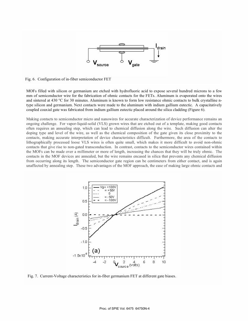
MOFs filled with silicon or germanium are etched with hydrofluoric acid to expose several hundred microns to a few
mm of semiconductor wire for the fabrication of ohmic contacts for the FETs. Aluminum is evaporated onto the wires
and sintered at 430 °C for 30 minutes. Aluminum is known to form low resistance ohmic contacts to bulk crystalline n-
type silicon and germanium. Next contacts were made to the aluminum with indium gallium eutectic. A capacitatively
coupled coaxial gate was fabricated from indium gallium eutectic placed around the silica cladding (Figure 6).
Making contacts to semiconductor micro and nanowires for accurate characterization of device performance remains an
ongoing challenge. For vapor-liquid-solid (VLS) grown wires that are etched out of a template, making good contacts
often requires an annealing step, which can lead to chemical diffusion along the wire. Such diffusion can alter the
doping type and level of the wire, as well as the chemical composition of the gate given its close proximity to the
contacts, making accurate interpretation of device characteristics difficult. Furthermore, the area of the contacts to
lithographically processed loose VLS wires is often quite small, which makes it more difficult to avoid non-ohmic
contacts that give rise to non-gated transconduction. In contrast, contacts to the semiconductor wires contained within
the MOFs can be made over a millimeter or more of length, increasing the chances that they will be truly ohmic. The
contacts in the MOF devices are annealed, but the wire remains encased in silica that prevents any chemical diffusion
from occurring along its length. The semiconductor gate region can be centimeters from either contact, and is again
unaffected by annealing step. These two advantages of the MOF approach, the ease of making large ohmic contacts and
Fig. 6. Configuration of in-fiber semiconductor FET
Fig. 7. Current-Voltage characteristics for in-fiber germanium FET at different gate biases.
Proc. of SPIE Vol. 6475 64750N-4

10h1_
iii 2IL) I I I I I I I
II I I I
II I I I
II I I I I
-109 -50 0 50 109
"qate voIts)
freedom from chemical diffusion, make it easier to avoid difficulties that preclude obtaining a fundamental
understanding of device behavior.
For germanium wires deposited within the MOFs with a diameter of 5 microns and length of 11mm, the resistivity from
two terminal measurements is 5.6x10⁻²
cm. Using a simple co-axial approximation the capacitance per unit length is
given by3:
C/L 2 0/ln(2h/r)
where is the dielectric permittivity of silica, h the radial thickness of the silica cladding, L the gate length and r the
radius of the semiconductor core.
For our germanium samples, these values are = 3.8, h = 47 microns, L = 1.5 mm and r = 2.5 microns, resulting in a
capacitance per unit length of 6 x 10-11
Fm-1
. As the gate bias voltage is varied from -100V to +100V (+/- 2.2x10⁶ Vm
-
1), the slope of the Idrain-Vsource curve increases (Figure 7), indicating that the carriers are n-type. The electron mobility
can be calculated as follows:
dIdrain/dVgate = µ(C/L2)Vsource-drain
where µ is the carrier mobility, which is 1.05 cm2/Vs at room temperature. The carrier density can be estimated by
calculating the total charge in the germanium wire as Q = CVthreshold, where C is the semiconductor wire capacitance and
Vthreshold the voltage necessary to completely deplete the device. Thus the total charge density is:
Ne = Q/e r2L.
Thus, taking, Vthreshold (pinch-off) as -100V and C = 9 x 10-14
F, Ne 2 x 10²¹
m-3
(or 2 x 10¹⁵
cm-3
).
Figure 8 shows how Idrain varies as a function of Vgate. The transconductance of the sample begins to be “pinched-off” at
voltages in the range of -90 to -100V. Thus this sample is functioning as a fiber-based depletion-mode FET switch.
While the experimentally available range of applied gate voltages limits characterization of the “off” regime of the FET,
we can estimate that the on/off current ratio of the device is 104 or better. Room temperature electron mobilities for bulk
polycrystalline devices are typically ~200 cm2/Vs.
4
Fig. 8. Drain current as a function of gate bias for in-fiber germanium FET.
Proc. of SPIE Vol. 6475 64750N-5

1.0L•
0.8 —
0.6 H
0.4 ——
-5 5 ID 15 2L•
In fiber
Etched from fiber
500 510 520
Raman shift (cm1)
Silicon reference
530
Fig. 9. Three terminal current-voltage characteristics for silicon in-fiber FET.
Fig. 10. Raman spectrum of silicon wire contained within fiber (top), after etching from fiber to bare silicon (mid-
dle), and silicon reference (bottom). There is a low frequency tail on the Raman mode for the silicon wire in the fi-
ber. This tail remains after etching the wire from the silicon to release strain caused by bonding of the silica to the
silicon and their thermal expansion mismatch. This tail is indicative of the presence of nanocrystalline or defective
silicon.
Proc. of SPIE Vol. 6475 64750N-6

6.ttE0
3.
0 W UD EO Z 2WTenp(I
=
x
xx
xx x
.6
We also made FET’s from silicon. For a silicon sample annealed at a temperature of 700 °C with a length of 18 mm
and cladding diameter of 125 µm, the measurements again indicate n-type carriers (Figure 9), with sample resistivity of
0.21 cm and device mobility of 1.4x10⁻²
cm2/Vs. For comparison bulk crystalline silicon is typically 10
2-10
3 cm
2/Vs.
5
The present samples have considerable nanocrystalline grains, as evidenced by tailing in the Raman spectrum to low
frequencies (Figure 10).3 More careful thermal annealing should allow for considerable reduction in the amount of this
nanocrystalline silicon and improved mobility. Extrapolation of the effect of Vgate on the transconductance allows us to
estimate Vpinch-off to be -320V, resulting in a free-carrier concentration of 6.6.x1015
cm-3
. The mobility of the silicon
samples is insensitive to temperature (Figure 11). Thus extrinsic scattering mechanisms, such as grain boundaries,
surface and charge traps are playing a dominant role in the transport, as expected from the presence of nanocrystalline
silicon in the samples determined from Raman spectroscopy. The conductivity ( ) vs. temperature (T) data for a
polycrystalline-Si sample can be fit to a function of the form (Figure 11):
(T) = A/ T exp(- /kT).
Here A is a semi-empirical constant and is an activation energy of the grain-barrier potential. The variation of
conductivity with temperature has been determined to vary in this way in the regime of grain-boundary limited
transport,6, 7
again in agreement with the conclusion that grain boundaries and defects currently dominate the transport
in the silicon in-fiber fibers.
Reducing the magnitude of grain boundary scattering is key to further progress towards device development. Higher
temperature annealing and/or alternative (e.g., laser based) annealing techniques are being explored towards this end.
1.2. Light Guiding in Fiber
We also characterized the light guiding properties of the silicon wires. Approximately 2 mm of the 125-µm diameter
silica cladding of a 5-cm-long sample was chemically etched away at one end. This was done to avoid the possibility
that light would be guided in the cladding instead of the silicon wire itself. 633 nm laser light launched at the opposite
end of the fiber stops propagating at the point where the glass cladding ends (Figure 12). In contrast, 1550 nm light
focused via a 0.65 NA 3.1mm focal length aspheric lens to 2µm at the core propagates all the way to the end of the fiber
(Figure 12). 100 mW of 1550 nm light resulted in an output power of 0.03 mW, resulting in an upper bound of 7 dB/cm
on the losses in the wire. Scattering from surface roughness is a critical component of the loss in planar silicon
waveguides because of the high index contrast between core and cladding. Our wires are fabricated within a template
that has 0.1 nm RMS surface roughness, which should make their outer diameter also very smooth. The inner diameter
Fig. 11. Conductivity and mobility of the silicon wires as a function of temperature.
Proc. of SPIE Vol. 6475 64750N-7

becomes relatively unimportant because its surface area is so small in the fiber geometry. Thus losses due to surface
roughness for semiconductor waveguides in the fiber geometry are easier to avoid.
1.3. Future Prospects for Integration
As the fundamental materials science described above to improve materials properties is pursued, an increased range of
devices will become possible. Semiconductor (and metal) heterojunctions can be integrated within the fiber (Figure 13)
by sequentially altering the precursors employed during deposition, giving rise to the possibility for incorporating a
633nm light; Stops when cladding ends
1550 nm light; Propagates to the end of the fibre
Fig. 12. Top: Schematic of the light guiding experiment showing the 2 µm diameter silicon core surrounded by the
etched, tapered cladding at the left end. Middle: 633 nm light stops propagating at the core-cladding boundary.
Bottom: 1550 nm light, in contrast, continues propagating to the end of the fiber. Some scatter is also evident at
the core-cladding boundary.
Fig. 13. Germanium-silicon radial heterojunction integrated into a microstructured optical fiber. Scale bar is 6
µm.
Proc. of SPIE Vol. 6475 64750N-8

broad range of optoelectronic functionality that can be engineered with such structures. In-fiber detectors that are
compact and integrate with existing fiber infrastructure may be possible. Optically or electrically pumped fiber lasers,
as mentioned previously, are another attractive target. Such a broad range of materials can be deposited by adapting
existing chemical vapor deposition (CVD) technologies that a very large number of devices can be imagined. Such
devices could be an important step forward in the pursuit of all-fiber optoelectronics.
Acknowledgements: V.G. and J.V.B thank the National Science Foundation (grant DMR-0502906), the Penn State Cen-
ter for Nanoscale Science MRSEC, funded by National Science Foundation grant DMR-0213623, and the Penn State-
Lehigh Center for Optical Technologies for support. J.V.B. also thanks the Office of Naval Research for support.
P.J.A.S. thanks the UK Engineering and Physical Sciences Research Council for support.
REFERENCES
1. Hunsperger, R. G. Integrated optics : theory and technology (Springer, Berlin ; New York, 2002).
2. Sazio, P. J. A., Amezcua-Correa, A., Finlayson, C. E., Hayes, J. R., Scheidemantel, T. J., Baril, N. F., Jackson,
B. R., Won, D. J., Zhang, F., Margine, E. R., Gopalan, V., Crespi, V. H. & Badding, J. V. Microstructured op-
tical fibers as high-pressure microfluidic reactors. Science 311, 1583-1586 (2006).
3. Finlayson, C. E., Amezcua-Correa, A., Sazio, P. J. A., Baril, N. F. & Badding, J. V. Appl. Phys. Lett., in press.
4. Meng, Z. G., Jin, Z. H., Bhat, G. A., Chu, P., Kwok, H. S. & Wong, M. On the formation of solid state crystal-
lized intrinsic polycrystalline germanium thin films. Journal of Materials Research 12, 2548-2551 (1997).
5. Mimura, A., Konishi, N., Ono, K., Ohwada, J., Hosokawa, Y., Ono, Y. A., Suzuki, T., Miyata, K. & Kawa-
kami, H. High-Performance Low-Temperature Poly-Si N-Channel Tfts for Lcd. IEEE Transactions on Electron
Devices 36, 351-359 (1989).
6. Dimitriadis, C. A. & Coxon, P. A. Hopping Conduction in Undoped Low-Pressure Chemically Vapor-
Deposited Polycrystalline Silicon Films in Relation to the Film Deposition Conditions. Journal of Applied
Physics 64, 1601-1604 (1988).
7. Kamins, T. I. Polycrystalline silicon for integrated circuit applications (Kluwer Academic Publishers, Boston,
1988).
Proc. of SPIE Vol. 6475 64750N-9


![Magneto-optical fibre sensors for electrical industry ... · Magneto-optical fibre sensors for electrical industry: analysis of perfo rmances - Optoelectronics [see also IEE Proceedings-Optoelectronics],](https://static.fdocuments.in/doc/165x107/5b76fde77f8b9ad2498bcd84/magneto-optical-fibre-sensors-for-electrical-industry-magneto-optical-fibre.jpg)