INTEGRATED INDUCTORS AND CAPACITORS WITH CO-LOCATED
80
INTEGRATED INDUCTORS AND CAPACITORS WITH CO-LOCATED ELECTRIC AND MAGNETIC FIELDS by Andy L. Schroedermeier A thesis submitted in partial fulfillment of the requirements for the degree of Master of Science (Electrical Engineering) at the UNIVERSITY OF WISCONSIN-MADISON 2016
Transcript of INTEGRATED INDUCTORS AND CAPACITORS WITH CO-LOCATED

INTEGRATED INDUCTORS AND CAPACITORS WITH CO-LOCATED
ELECTRIC AND MAGNETIC FIELDS
by
Andy L. Schroedermeier
A thesis submitted in partial fulfillment of the
requirements for the degree of
Master of Science
(Electrical Engineering)
at the
UNIVERSITY OF WISCONSIN-MADISON
2016


i
Abstract Passive components such as inductors and capacitors are fundamental components
needed in all power electronics converters, and in many designs, they comprise a
significant portion of the total weight and volume of the converter. As more renewable
energy is added to the grid, and hybrid and electric powertrains become more common in
the automotive industry, power electronic systems to convert energy between different
types of sources and loads will be of increasing importance.
In order to improve upon power electronic conversion circuits, this thesis presents
an innovative method for decreasing the cost, size, and weight of power electronic
converters by integrating the electric field of a capacitor with the magnetic field of an
inductor into a common volume. In this new method, the parallel plates of a stacked or
rolled film capacitor are also utilized as the permeable laminations of the inductor core.
This two terminal capacitor can then be wound with a separate two terminal inductor
winding. This device is dissimilar from existing integration techniques, which integrate the
terminals and arrange the discrete electric and magnetic fields in close proximity to each
other. The proposed device improves upon existing technologies by allowing the
possibility of volume reduction, weight reduction, and packaging efficiencies, while
keeping the two inductor and two capacitor terminals galvanically isolated.
The proposed device is analytically modeled and the fields in the core are analyzed.
While the terminals are galvanically isolated, cross coupling of the fields is examined. Two
different proof-of-concept prototypes are constructed and tested to verify the analytical
models. One of the devices is tested in boost converter circuit application.

ii
A basic design procedure is developed for the proposed device that allows the use
of a volume minimization routine to reduce the overall size. Several tradeoffs and material
and geometry issues are discussed. Finally, several candidate manufacturing processes are
evaluated.

iii
Acknowledgements I would like to thank my advisor Professor Ludois for his support and
encouragement. I would like to thank the Wisconsin Electric Machines and Power
Electronics Consortium (WEMPEC), the Department of Electrical and Computer
Engineering, and the Wisconsin Alumni Research Foundation (WARF) for their continued
support of this research. I would also like to thank my fellow graduate students for their
support and assistance around the lab. Finally, I would like to thank Linda and Bram.
Without their unwavering support and continual encouragement, none of this would have
been possible.

iv
Table of Contents
Abstract ............................................................................................. i
Acknowledgements .......................................................................... iii
Table of Contents ............................................................................ iv
List of Figures ................................................................................. vi
List of Tables ................................................................................... ix
Nomenclature ................................................................................... x
Introduction ...................................................................................... 1
Chapter 1: Background ................................................................ 3
1.1 Historical Perspective ......................................................................... 3
1.2 Current State of the Art ...................................................................... 4
1.2.1 Wound Film Capacitor Terminal Integration ............................................... 4
1.2.2 Plate Capacitor Terminal Integration ............................................................ 6
1.2.3 Magnetic and Electric Field Integration of Inductors and Capacitors .......... 7
1.3 Summary ............................................................................................ 9
Chapter 2: Model of Co-Located Electric and Magnetic Fields in a Rolled Dual Energy Core ....................................................... 10
2.1 Integrated Inductor and Capacitor with a DEC ................................ 10
2.2 Comparison to Previous Work ......................................................... 12
2.3 Analytical Model of Fields in Core .................................................. 13
2.4 Field Interaction ............................................................................... 16
2.4.1 Mutual Coupling in the Magnetic Field ...................................................... 16
2.4.2 ESR Influence ............................................................................................. 19
2.5 Summary .......................................................................................... 20
Chapter 3: Experimental Verification of Models ...................... 22
3.1 Prototype Devices ............................................................................ 22
3.1.1 Device 1 ...................................................................................................... 22
3.1.2 Device 2 ...................................................................................................... 23

v
3.2 Small-Signal Verification of Decoupled Fields ............................... 25
3.3 Verification of Decoupled Fields in a Power Circuit ....................... 29
3.4 Summary .......................................................................................... 33
Chapter 4: Integrated Device Design ........................................ 34
4.1 Design Tradeoffs .............................................................................. 34
4.1.1 Conductor Thickness in Core ...................................................................... 34
4.1.2 Temperature ................................................................................................ 35
4.1.3 Parasitic Equivalent Series Inductance ....................................................... 36
4.2 Design Considerations ..................................................................... 39
4.2.1 Material Selection ....................................................................................... 39
4.2.2 Geometry Selection ..................................................................................... 42
4.3 Design Procedure ............................................................................. 43
4.4 Volume Minimization ...................................................................... 46
4.5 Manufacturing Considerations ......................................................... 49
4.5.1 Vapor Deposition ........................................................................................ 49
4.5.2 Film-Foil ..................................................................................................... 51
4.5.3 Reduced Manufacturing Processing ........................................................... 52
4.6 Summary .......................................................................................... 53
Chapter 5: Conclusion ............................................................... 55
5.1 Summary .......................................................................................... 55
5.2 Key Contributions ............................................................................ 56
5.3 Recommended Future Work ............................................................ 58
References ...................................................................................... 60
Appendix I ...................................................................................... 63
Appendix II ..................................................................................... 65

vi
List of Figures Figure 1-1 Inductor-capacitor hybrid device based on [4] shown in a low pass filter
configuration. .......................................................................................................... 5
Figure 1-2 Planar integrated inductor and capacitor based on [7] shown in a low pass
filter configuration. ................................................................................................. 6
Figure 1-3 Schematic depiction of a discrete capacitor depicting electric field lines and a
discrete inductor depicting magnetic field lines (a). Depiction of a terminal
integrated device (b) and a depiction of electric field and magnetic field
coexisting in the same volume with a four terminal device (c). ............................. 8
Figure 2-1 Sectioned model and dimensioned cross-section view of integrated device.
Note the thicknesses (d and δ) of the alternating layers in the core are exaggerated
for clarity. .............................................................................................................. 11
Figure 2-2 Approximation of the spiral core as concentric circles with individual
reluctance paths(a), and a magnetic circuit model of the core(b). ........................ 15
Figure 2-3 Diagram of a toroidal integrated device core showing the inductor and
capacitor current orientations. ............................................................................... 17
Figure 2-4 Example plot of the capacitor current contribution the the DEC B-field. ...... 19
Figure 2-5 Measured ESR of a film capacitor as a function of the magnetic field applied
to the device by a separate inductor winding. ....................................................... 20
Figure 3-1 Prototype Devices 1 (a) and 2 (b). .................................................................. 22
Figure 3-2 Winding jig used to make the core of device 2. .............................................. 23
Figure 3-3 Schematic depiction of four different impedance tests. .................................. 26

vii
Figure 3-4 Measured impedance vs. frequency of Device 1 (top) and Device 2 (bottom)
measured separately at the capacitor terminals and the inductor terminals. ......... 27
Figure 3-5 Modeled and measured series and parallel connection of the DEC inductor and
capacitor for devices 1 and 2. ............................................................................... 28
Figure 3-6 Boost converter utilizing device 1 as the input inductor and output capacitor
(a), and circuit diagram showing the inductor and capacitor on opposite sides of
the SPDT switch (b). ............................................................................................. 30
Figure 3-7 Measured voltage and current waveforms of the boost converter in operation.
............................................................................................................................... 31
Figure 3-8 Thermal image of the boost converter at steady state under load. .................. 32
Figure 4-1 Inductance and capacitance versus premeable conductor thickness for a
constant core volume. ........................................................................................... 35
Figure 4-2 DEC device with extra ESL (a) and without extra ESL (b). ........................... 36
Figure 4-3 View of device 3 core with inductor windings removed to show concentric
electric field and magnetic field core arrangement. .............................................. 37
Figure 4-4 Impedance vs. frequency of device 3 as seen at the inductor and capacitor
terminals. ............................................................................................................... 38
Figure 4-5 Device 3 impedance vs frequency at the capacitor terminals with and without
current loop cancellation. ...................................................................................... 39
Figure 4-6 Comparison of normalized conduction loss for different conductor materials
as a function of conductor thickness. .................................................................... 40
Figure 4-7 Concepts for possible integrated device geometries. ...................................... 43

viii
Figure 4-8 DEC device volume when varying the core inner diameter D1 and the core
height h.................................................................................................................. 48
Figure 4-9 Roll of plastic film with nickel-cobalt vapor deposition. ................................ 50
Figure 4-10 Edge quality comparison of a sample of nickel foil to aluminum foil used in
film capacitor manufacturing. ............................................................................... 52
Figure 4-11 Manufacturing steps for discrete inductors and capacitors. The steps in
circles can be eliminated with the integrated design. ........................................... 53

ix
List of Tables Table 2-1 Comparison of Integration Concepts ................................................................ 13
Table 3-1 Device Capacitance Data .................................................................................. 25
Table 3-2 Device Inductance Data .................................................................................... 25
Table 3-3 Inductance and Capacitance of Device 1 in Operation .................................... 32
Table 4-1 Comparison of Core Conductor Materials ....................................................... 41
Table 4-2 Comparison of Core Dielectric Materials ......................................................... 42
Table 4-3 Volume Comparison of Different Device 1 Designs ....................................... 49

x
Nomenclature ε0 Vacuum Permittivity [F/m]
εr Relative Permittivity
w Dielectric and Conductor Material Width [m]
l Dielectric and Conductor Material Length [m]
d1 Dielectric Material Thickness [m]
d2 Air Gap Thickness [m]
µr eff Effective Permeability of DEC Core
µr Relative Permeability
µ0 Vacuum Permeability [H/m]
N Number of Inductor Turns
h DEC Core Height [m]
D1 DEC inner diameter [m]
D2 DEC outer diameter [m]
a DEC inner radius [m]
b DEC outer radius [m]
R Magnetic Reluctance [H-1]
δ Conductor Material Thickness [m]
rci Conductor Coil Radius [m]
rdi Dielectric Coil Radius [m]
C Capacitance [F]
L Inductance [H]
A Wire Area [m2]

xi
FF Winding Fill Factor
SF Stacking Factor
I Current [A]
V Voltage [V]
F Frequency [Hz]
1
Introduction Power electronic circuits are integral to everyday life, and researchers continue to
find more and more applications for power electronics. No matter the size or power level
of the system, passive components such as inductors and capacitors are essential to
converter operation. Since these devices can be some of the largest and heaviest
components in power electronic circuits, they represent a big opportunity for cost, volume,
and weight reduction via integration.
Chapter 1 reviews the current state of passive component integration in the power
electronics field. The benefits and drawbacks of the different approaches are compared and
contrasted.
Chapter 2 introduces an innovative integrated inductor and capacitor design in
which the electric field of the capacitor and magnetic field of the inductor is stored in the
same core volume of the integrated device. This core is called a dual energy core (DEC).
In order to understand the fields in this device, an analytical model is developed to predict
the terminal inductance and capacitance. The model is then further refined in order to
account for parasitic interactions.
Chapter 3 uses several different experimental proof-of-concept prototypes to
validate the analytical model. The small-signal frequency response plots are examined and
compared to models of discrete devices. In addition, operation of a prototype device is
demonstrated in a circuit application operating as both the input inductor and output
capacitor of a boost converter.
Chapter 4 presents design and volume minimization principles. First, several design
tradeoffs, material selection and geometry selection issues are discussed. Then, an example

2
design procedure is presented and subsequently iterated to find the smallest volume
possible for that application. Finally, manufacturing considerations for the two most
prevalent types of rolled film capacitor manufacturing are discussed.
Chapter 5 provides a summary of the work presented, and lists the key contributions
to the research literature. Several recommendations for future work are provided.

3
Chapter 1: Background 1.1 Historical Perspective
The fundamental functions of power electronic converters have been characterized
as the switching, conduction, electromagnetic energy storage, information, heat exchange,
and mechanical/structural functions [1]. These functions are general to all types of
switching power converters at all energy levels. In the past several decades, some of these
functions have undergone more changes than other functions. There have been many types
and different generations of semiconductor switches, for example, including Si diodes,
thyristors, BJTs, IGBTs, MOSFETs, IGCTs, and now SiC and GaN devices. However, the
electromagnetic energy storage function that enables the continuous flow of energy when
sources are interrupted by switches has not undergone nearly as much fundamental change.
Inductors and capacitors, the two components that store energy over parts of the
switching cycle in a power converter, are used because of their properties that allow them
to smooth out currents and voltages, respectively. These properties are useful as
intermediate storage states in power electronic circuits. In many designs, the passive
components comprise a significant amount of the weight and volume of the converter. Even
in volume optimized designs with high power densities such as the converters used in the
automotive industry, the passive components take up a significant volume of the package
as a whole [2].
To date, the dominant method of passive component minimization has been through
increases in switching frequencies enabled by successive semiconductor device
improvements. However, further minimization will require research into passive
components and cooling technologies using such techniques as multi-functional integration

4
[3] among others. Realizing that volume reduction is possible through integration of
inductive and capacitive components, integrated inductors and capacitors have been of
interest for several decades.
However, commercialization of integrated components has been difficult and
current inductor and capacitor integration techniques have inherent drawbacks that limit
their use to only a subset of applications. As a result, almost all power electronic circuits
in commercial use today utilize discreet inductors and capacitors in their designs. Weight
and cost reduction are also possible by integration, but they have not been explored as
thoroughly in the literature, with most researchers focusing on volume minimization as
discussed next.
1.2 Current State of the Art
A number of researchers have worked on the topic of passive component integration
for the purpose of volume minimization. Integration of inductors and capacitors is typically
accomplished by terminal integration of the device, with the geometry arranged so that the
electric and magnetic fields are in close proximity. This results in a three terminal device
that can be used in applications such as power electronic filters where connected networks
of inductors and capacitors are required. However, it is not possible to access the inductor
and capacitor individually in these designs, meaning that there is no galvanic isolation
between the inductor and capacitor terminals, which is the chief limitation of terminal
integrated designs.
1.2.1 Wound Film Capacitor Terminal Integration
One way to accomplish this terminal integration is by winding a film capacitor
around a permeable core and routing the current through the capacitor plates such that it

5
travels in a spiral around the core, inducing a magnetic field. This design is shown in
Figure 1-1 which is based on the original publication of the concept in 1976 [4]. The device
is drawn in a low pass filter configuration with capacitance exhibited between terminals 1
and 2, and inductance between terminals 1 and 3. Note that terminal 3 is connected to the
same capacitor plate as terminal 1. Very little was done with this specific embodiment until
more recently, where it has been proposed as a filter in an AC machine drive [5], and as
the boost inductor and EMI filter for a power factor correction converter [6].
Terminal 1Terminal 2Terminal 3
MagneticCore
Figure 1-1 Inductor-capacitor hybrid device based on [4] shown in a low pass filter configuration.
One of the major limitations of this embodiment is that the current path through the
capacitor is carried by a long, thin conductor, which is wrapped around the permeable core
in order to create an inductance effect. Because of this, the device may incur significant
resistive losses if the current capability is not sufficiently limited. If higher current is
needed, the conductor thickness must be increased, which may negate any volume
reduction for this device. Note that in this device, the electric field is in the dielectric

6
material between the foil layers and the magnetic field is in the magnetic core or core air
gap. Therefore, there is no integration of the fields, only the terminals, meaning that
independent access to the inductive and capacitive properties of this device is not possible.
1.2.2 Plate Capacitor Terminal Integration
In another embodiment of the terminal integrated device, this same effect can be
realized with a plate capacitor instead of a rolled film capacitor construction. In this design,
the capacitor is also geometrically arranged around a magnetically permeable core as
shown in Figure 1-2, which is a drawing based on [7]. This embodiment has seen
significantly more research and has been used as an EMI filter for a distributed power
system converter [8] [9], as an EMI filter for a high intensity lamp ballast [10] [11] [12]
and in DC-DC converters [13].
Metallized Dielectric
Terminal 1
Terminal 2Terminal 3
FerriteCore
Figure 1-2 Planar integrated inductor and capacitor based on [7] shown in a low pass filter configuration.
In this design, as with the previous one, the current on the capacitor plates is
directed so that it loops around the permeable core, increasing the series inductance caused
in the capacitor current path. Figure 1-2 shows connection call outs for a low pass filter

7
topology in the same manner as the previous device where capacitance is exhibited between
terminals 1 and 2, and inductance between terminals 1 and 3 which are both connected to
the same metallization layer of the capacitor.
1.2.3 Magnetic and Electric Field Integration of Inductors and Capacitors
Since electric field energy and magnetic field energy is stored in two discrete
locations in the terminal integrated devices, volumetric reduction is limited and it has not
been well documented in the literature. In addition, separate magnetic field and electric
field cores are still required, which limits weight and cost optimization.
However, there is no physical law requiring electric field and magnetic field energy
to be stored in discrete locations; and magnetic and electric field integrated devices have
the possibility of much tighter integration. Currently, electric field energy and magnetic
field energy exist in discrete components as depicted in Figure 1-3a. Alternatively, in the
case of the terminal integration concepts in the previous sections, the field energy is stored
in discrete locations in a three terminal integrated device as depicted in Figure 1-3b. Here
the B field is in the magnetic core, and the E field is between the layers of windings around
the outside of the core.
With the field integration concept, it is possible to have the fields coexist in the
same volume as depicted in Figure 1-3c, where both the B field and the E field exist in the
dielectric material between the capacitor conductors. This topology has the added benefit
of decoupled properties at the inductor and capacitor terminals. In this way, the inductor
and capacitor terminals can be connected in series, parallel, or even in separate parts of the
circuit.

8
Magnetic and electric field integration of inductors and capacitors has not been
proposed previously in the scientific literature by other authors. The only known reference
to this type of integration has been patented in [14], which represents the only known
publication prior to this work of a truly field integrated, terminal decoupled device.
However, the preferred embodiment in this patent is difficult to manufacture using existing
techniques and lends limited functionality in power electronics.
i
Discrete Capacitor Discrete Inductor(a)
L & C fields in same volume(c)
iL & C terminal integration
(b)
+
+
+
+
+
+
+
+
+
+
+
+
+
+
+
+
-
-
-
-
-
-
-
-
-
-
-
-
-
-
-
-
+ V -
+ + + + + + + + + +
- - - - - - - - - -
+V-
+ + + + + + + + + +
- - - - - - - - - -
+V-
i
E
B
B
E
B
E
Figure 1-3 Schematic depiction of a discrete capacitor depicting electric field lines and a discrete inductor depicting magnetic field lines (a). Depiction of a terminal integrated device (b) and a depiction of electric field and magnetic field coexisting in the same
volume with a four terminal device (c).

9
This thesis introduces an integration concept in which the electric field and
magnetic field share a common volume, the inductor and capacitor terminals are largely
decoupled, and the device is easy to manufacture using existing techniques developed in
the film capacitor and inductor industries. This device was patented in [15] and portions of
this research were published at the 2015 IEEE Energy Conversion Congress and Exposition
(ECCE) in [16] and has been selected to appear in the IEEE Transactions on Industry
Applications [17].
1.3 Summary
• Two different types of inductor and capacitor integration technologies are briefly
reviewed. The first two are terminal integration techniques that leave the electric
and magnetic fields parsed. They work by exploiting and enhancing parasitic
inductive properties inherent in capacitor designs.
• A new method, which integrates the electric and magnetic fields into a common
volume, is introduced. This new method utilizes the plates of a stacked or rolled
film capacitor as the permeable laminations of the inductor core, which is wound
with a separate inductor winding to create a four terminal device with largely
decoupled inductive and capacitive properties. This method has not been previously
analyzed or tested and it is the focus of this work.

10
Chapter 2: Model of Co-Located Electric and Magnetic Fields in a Rolled Dual Energy Core
The device examined in this thesis combines the electric field and magnetic field
energy into a common volume in what is termed a dual energy core (DEC). This device
has 4 terminals, two each for the inductor and capacitor. The inductor terminals and
capacitor terminals can be accessed independently, and from a circuit perspective, they
appear as decoupled, lumped elements in most cases.
2.1 Integrated Inductor and Capacitor with a DEC
Figure 2-1 shows a cross section view of a toroidal form factor DEC device. Other
form factors are possible and are discussed briefly in section 4.2.2, but the toroidal form
factor is the focus of this work. In this device, the DEC is created by rolling alternating
layers of conductor and dielectric material into a toroid to form a film capacitor. This
technique is nearly identical to traditional film capacitor winding. An integrated inductance
is realized by winding wire around the toroid in a manner identical to traditional toroidal
inductor construction, inducing magnetic flux circumferentially around the core. The
capacitor conductors can be made of magnetically permeable material to intensify the
magnetic flux density. This field is shown going in and out of the page in Figure 2-1b.
Capacitance is exhibited between the conductive layers in the dielectric material,
and is shown as arrows in Figure 2-1b. This field is orthogonal to the magnetic field
induced by the inductor winding. Connections are made to the capacitor by shorting one
capacitor conductor winding across the top of the device and the other conductor winding
across the bottom of the device to allow for good current flow even with very thin
conducting layers in the core. This process is referred to as end spray in the film capacitor

11
industry. The end spray technique is an improvement over previous terminal integrated
designs where shorting each spiral winding on one end to minimize the capacitor ESR and
increase current capability was not possible since shorting the conductors would have
negated the inductance effect in those designs.
Figure 2-1 Sectioned model and dimensioned cross-section view of integrated device. Note the thicknesses (d and δ) of the alternating layers in the core are exaggerated for
clarity.
The dielectric material may be chosen with a relative permittivity greater than 1 in
order to maximize the capacitance effect. The capacitor conductors in the core may be

12
chosen to have a relative permeability greater than 1 (e.g. nickel or iron) in order to
maximize the inductance effect in the core as previously mentioned.
2.2 Comparison to Previous Work
The proposed device with a DEC has numerous advantages over previous work as
detailed in Table 2-1. The table compares several attributes that differentiate the DEC
design from previous work. The first property is manufacturability, which considers
whether new manufacturing technologies or techniques are need to produce the component.
The second property is elimination of the discrete magnetic core, which shows that the
DEC device eliminates the material and manufacturing cost of a discrete magnetic core.
The third property is decoupling of the L and C terminals, which differentiates between
four terminal devices with independent L and C terminals, and three terminal devices,
which are inherently coupled. The fourth property concerns the current capability of the
capacitor, which is higher when the capacitor windings can be shorted on one side. The
final property examined is the location of the field energy, meaning whether or not the
electric and magnetic fields occupy the same volume.
Compared to the device patented in [14], the device proposed here is much easier to
manufacture, and it eliminates the heavy, separate magnetic core that is present in the
preferred embodiment of the patent. Compared to the two different terminal integrated LC
filter designs, the device proposed here has the benefit of eliminating the separate magnetic
core. In addition, it also has the advantage of decoupled inductor and capacitor terminals
that allow the inductor and capacitor to be connected in series, parallel, or in separate parts
of the circuit. The integrated filters only allow a distributed connection since they are
terminal integrated devices.

13
Table 2-1 Comparison of Integration Concepts
Property Proposed Device Ref. [14] Planar LC
Filter Wound
LC Filter
Manufactured with existing techniques Yes No Yes Yes
Elimination of separate magnetic core Yes No No No
Decoupled L & C terminals Yes Yes No No
High current capability Yes Yes Yes Maybe
Co-located fields Yes Yes No No
2.3 Analytical Model of Fields in Core
The fields in the DEC exist in a decoupled fashion in most designs and can be
measured and modeled independently at their respective terminals based on the properties
of the materials, and the dimensions given in Figure 2-1. Note that the thicknesses of the
conductor δ and the dielectric d in the core have been exaggerated for clarity in the figure.
The capacitance of the device as seen at the capacitor terminals is given in (2-1),
which is a standard parallel plate capacitance equation, where the materials in the core have
width w and unrolled length l. The equation has been modified with two different dielectric
materials, which are the plastic film and an air gap with relative permeabilities εr1 and εr2,
respectively. Note that for air, εr2 = 1. In addition, the factor of two in the numerator
accounts for the fact that there are two layers of dielectric material in the core in wound
film capacitor construction, making the capacitor double-sided when rolled up. The
conductor material has thickness δ. In this case, d from Figure 2-1 equals d1+d2, which is
the dielectric thickness plus the air gap thickness. The inclusion of an air gap in the model
is needed since it is difficult to eliminate the air gap entirely. Even when rolling the films

14
under tension in the typical rolled construction of film capacitors, a small amount of air
will remain and it may affect the capacitance of the device.
C = 2εowl
d1
εr1 +
d2
εr2
(2-1)
The inductance seen at the inductor terminals is given in (2-2) where µr eff is the
relative permeability of the core as a whole. This equation is a standard toroidal inductor
equation where N is the number of inductor turns, h is the core height, D1 is the core inner
diameter, and D2 is the core outer diameter.
L = µr effµoN2h
2π ln
D2
D1 (2-2)
When the DEC is made entirely of materials with the same magnetic relative
permeability, such as µr = 1 for both the aluminum and plastic film typically used in film
capacitor construction, then µr eff = 1. However, when the DEC is made of materials with
different relative permeabilities, the effective permeability of the DEC as a whole is not
known, and another approach must be used to calculate the relative permeability of the
DEC µr eff.
One way to calculate µr eff when the relative permeabilities of the materials in the
core differs is to calculate the reluctance of the magnetic circuit as shown in (2-3). Since
the material in the core forms a spiral, it is not easy to calculate a closed magnetic circuit.
However, since the layers are very thin and the distance around the spiral is much greater
than the distance between layers, it is appropriate to approximate the spiral as alternating
concentric circles of dielectric and conductor materials as shown in Figure 2-2a.

15
Rc1 Rd1 Rc2 Rd2 ... Rc1 Rc2 Rc3ReqReq ≈
Rci Rdi
≈ =
(a)
(b)
ri
r1
...
Figure 2-2 Approximation of the spiral core as concentric circles with individual
reluctance paths(a), and a magnetic circuit model of the core(b).
The equation in (2-3) can be further simplified for the typical case where d and δ
are much less than D1 and therefore rci and rdi are practically identical for each i. This
allows for the simplification in (2-4). Furthermore, for the specific cases where the
reluctance of the conductor material Rc dominates, the reluctance contribution of the
dielectric material Rd is negligible and may be ignored as shown in Figure 2-2b.
L = N2
R = N2
2π
µrcµoδw
∑i=1
nrci
-1
-1
-1
+
2π
µrdµoδw
∑i=1
nrdi
-1 -1
-1
-1 (2-3)
L ≈ 1
2π N2µow(µrcδ+µrdd) ∑i=1
nri
-1 (2-4)
By equating (2-2) and (2-4), the effective permeability of the core as a whole µr eff
can be calculated. The result, shown in (2-5) gives the effective permeability of the core as
a whole. It can be shown to be equivalent to a more typical stacking factor calculation of
core permeability used to characterize laminated magnetic cores. A systematic derivation
16
of the stacking factor equivalency presented in (2-5) is included in Appendix I. In (2-5),
the stacking factor SF is the ratio of the thickness of magnetically permeable material with
permeability μrc to the total layer thickness. The stacking factor calculation is scaled by the
ratio of the conductor width to the core height if they are different. This equation allows
for a simple approximate calculation of the permeability of the core as a whole, based only
on physical dimensions of the materials used to create the core.
µr eff = w(µrcδ+µrdd)
hln
D2
D1
∑i=1
nri
-1 -1
wh [ ]SFµrc+(1-SF)µrd (2-5)
2.4 Field Interaction
It has been stated that the electric field and magnetic field that exist in the core of
the device exhibit decoupled behavior as seen at the device terminals, meaning that the
inductor and capacitor can be treated as discrete elements. However, this assumption does
break down under certain circumstances and the cross-coupling effects must be included.
Two cases to be examined here are the influence of the capacitor current on the inductor
magnetic field, and the influence of the magnetic field in the core generated by the inductor
on the charge distribution of the capacitor conductor.
2.4.1 Mutual Coupling in the Magnetic Field
The capacitor current flows primarily in the axial direction through the DEC,
meaning that the current enters the core through the top end spray, and exits through the
bottom end spray as indicated in Figure 2-3. This current flow induces an azimuthal
magnetic field. The AC portion of this magnetic field that resides inside the DEC will
contribute to the AC voltage seen at the inductor terminals due to Faraday’s Law. This is
the first possible method of interaction in the core between the inductor and capacitor.

17
The magnitude of this field induced by the capacitor is also dependent on whether
or not the negative terminal of the capacitor is passed back up through the middle of the
core. This pass back arrangement is commonly used to tailor the equivalent series
inductance (ESL) of wound film capacitors.
Figure 2-3 Diagram of a toroidal integrated device core showing the inductor and
capacitor current orientations.
Using the geometry depicted in Figure 2-3, the B field in the DEC can be
determined as shown in (2-6) for the case where the negative capacitor terminal does not
pass back through the middle of the core. Here, the B field in the core is a function of the
current enclosed in the Amperian loop. There is both inductor current Il and capacitor
current Ic enclosed as shown in (2-6). When the negative terminal pass back is included,
the B field in the core is slightly different due to the different capacitor current path, and
the resulting field can be found using (2-7). For both cases, the inductor current Il passes
through N inductor turns, a is the DEC inner radius, and b is the DEC outer radius.
Given the two B field equations, the total flux in the toroidal core can be calculated
as shown in (2-8) without the negative terminal pass back, and in (2-9) with the negative
terminal pass back. Here the flux is calculated by integrating the B field determined in the

18
previous equations, and the resulting flux is slightly different depending on the capacitor
current setup.
Bno_return = µoµrIenc
2πr = b2-a2µoµr
2πr
IlN+Ic
r2-a2 (2-6)
Bwith_return = µoµr
2πr
IlN+Ic
r2-a2
b2-a2 - 1 (2-7)
Φwith_return = ⌡⌠B∙dA = a + µoµrhIc
2πr
1
2 -
1 +
a2
b2-a2 lnb
aµoµrNIl
2πr lnb
(2-8)
Φno_return = ⌡⌠B∙dA = a + µoµrhIc
2πr
1
2 - a2
b2-a2lnb
aµoµrNIl
2πr lnb
(2-9)
As can be seen from (2-6), the B field in the DEC is a function of both the inductor
amp-turns and the capacitor current. For the case where the capacitor and inductor
terminals of the device are series connected, the B field due to the inductor amp-turns will
dwarf the B field contributed by the capacitor current if any appreciable number of inductor
turns are used. In this situation, the influence of the capacitor current on the magnetic field
can be essentially ignored as long as the saturation flux is not approached. In applications
where the inductor and capacitor are connected in separate parts of the circuit, the level of
field interaction will depend on the device geometry and the relative magnitudes of the
capacitor and inductor currents as well as the number of inductor turns N. To ensure that L
and C are essentially decoupled, simply design the inductor amp-turn product to be at least
an order of magnitude higher than the capacitor current during operation.
The magnitude of the B field due to the capacitor current is dependent on whether
the negative capacitor terminal is passed back through the center of the core. Figure 2-4
gives an example of the relative magnitudes of the B field due to the capacitor as a function
of radius. With no pass back, there is no field in the center of the device. In this case, the

19
field increases from a to b, and then begins to decrease as the radius heads toward infinity.
For the case where the negative capacitor terminal is passed back through the center, the
field magnitude will exist in the center, as well as in the DEC, but it will be zero outside
the DEC at radii greater than b. The decision on whether to pass the negative terminal back
through the core is application dependent, and depends on the location and amount of
magnetically permeable material in the device among other things.
Figure 2-4 Example plot of the capacitor current contribution the the DEC B-field.
2.4.2 ESR Influence
The second form of interaction in the core relates to current distribution on the
capacitor conductors. The magnetic field induced in the DEC by the inductor turns can
influence the distribution of charge on the capacitor conductors by causing the current to
crowd toward the edges of the conductor material. For a typical DEC design, however, the
conductor material is micron-scale thickness. Therefore, even for applied AC fields at
100 kHz, the skin depth of the conductor material is much greater than the conductor
material thickness, effectively negating the applied magnetic field influence on the
capacitor conductor current distribution.

20
Figure 2-5 gives the measured ESR at the terminals of a 50 volt, 80 μF capacitor
(forming a DEC) as a function of the magnetic field applied to the core. Two different
fields are applied to the device core via a separate inductor winding: a DC magnetic field,
and a 10 kHz AC field. The ESR of the capacitor does not change appreciably in either
case, suggesting that the capacitor conductor material is sufficiently thin to avoid current
crowding issues at the applied frequency.
Figure 2-5 Measured ESR of a film capacitor as a function of the magnetic field applied
to the device by a separate inductor winding.
As long as the AC field caused by the inductor is of a low enough frequency to
avoid skin depth issues on the capacitor conductor, this parasitic coupling effect can be
ignored. Due to the thin conductors used in practical film capacitor designs, and the
inherent frequency limitations in circuits utilizing wound film capacitors, this effect will
likely not be encountered.
2.5 Summary
• In this chapter, one type of DEC device was introduced. Its features and properties
were compared and contrasted with previous work, and the DEC device was found
to have beneficial properties for easy manufacturing and potential uses in the

21
broadest array of applications. The DEC also eliminates the discrete magnetic core
required in the other designs.
• An analytical model of the DEC device was developed for the capacitance and
inductance of the device as seen at the terminals. This model was refined for the
case where a spiral of magnetically permeable material is present in the core by
approximating the spiral as concentric circles of magnetic material. The spiral
rolling constitutes a distributed magnetic air gap.
• Two different types of interactions between the electric and magnetic fields in the
core were uncovered and examined. The first is the effect of the capacitor current
on the flux linkage seen at the inductor terminals. This effect is minimal as long as
the inductor amp-turn product is at least an order of magnitude greater than the
capacitor current in the application.
• The second interaction between L and C is the effect of the magnetic field caused
by the inductor on the capacitor current distribution in the core. This effect is small
as long as the capacitor conductors are thinner than the skin depth at the applied
inductor frequency, and it is not an issue in practical designs with thin capacitor
conductors.

22
Chapter 3: Experimental Verification of Models 3.1 Prototype Devices
The previous section lays out an analytical model of the DEC device. In order to
verify experimentally the analytical model, and also verify that the magnetic and electric
fields in the core appear as lumped, decoupled elements, two non-optimized, prototype
devices featuring a DEC were constructed. These devices have four terminals. Two of the
terminals are inductor terminals and the other two terminals are capacitor terminals. The
two devices that were constructed for the experimental verification are shown in
Figure 3-1.
Figure 3-1 Prototype Devices 1 (a) and 2 (b).
3.1.1 Device 1
The core of device 1 is a plastic film capacitor made with polyethylene terephthalate
(PET) plastic film with a vapor deposited aluminum conductor. Two layers of this film
were rolled into a toroid. This film capacitor was manufactured using industry-standard
processes. One of the vapor deposited conductors has been shorted with end spray on the

23
top of the device, and the other has been shorted on the bottom of the device in order to
form two capacitor terminals. This capacitor is then wound with wire to form a toroidal
inductor with two separate terminals. The two capacitor terminals and two inductor
terminals are labeled in Figure 3-1 as C+, C-, L+, and L-. Note that since the core of
device 1 is made of plastic and aluminum, the effective relative permeability of the core
μreff is 1.
3.1.2 Device 2
The core of device 2 was formed by winding alternating layers of PET plastic film
and steel foil into a toroid in a manner similar to film-foil capacitor construction. Since
capacitor manufacturing with magnetically permeable materials has not yet been
commercially developed, this prototype was constructed by hand with a homemade
winding jig. The winding jig used to create this core is shown in Figure 3-2.
Figure 3-2 Winding jig used to make the core of device 2.
Due to manufacturing limitations of a handmade core, the steel foil was not shorted
on the top and bottom, and the capacitor connections are made only at the end of each roll

24
of foil. This core was then wound with wire to form a toroidal inductor. Again, the device
has two inductor terminals and two capacitor terminals as labeled in Figure 3-1. For this
device, the addition of magnetically permeable steel into the core causes μr eff to be 21.86,
greatly increasing the permeability of the core over device 1.
The material properties and dimensions of devices 1 and 2 for calculating
capacitance are shown in Table 3-1 and the dimensions and properties for calculating
inductance are given in Table 3-2. These dimensions and material properties were plugged
into (2-1) and (2-2) in order to calculate the expected inductance and capacitance of the
devices. In addition, the capacitance and inductance of each device was measured at the
terminals using an LCR meter. These calculation and measurement results are also shown
in Table 3-1. The calculated and measured values of inductance and capacitance correlate
well with each other and show that the analytical inductance and capacitance calculations
are valid.
Device 1 is more capacitive than inductive, because the capacitor in the core was
professionally made with very thin films and no air gap, and since there is no magnetically
permeable material in the core. Device 2 is more inductive than capacitive. The inductance
is higher because of the magnetically permeable steel in the core. The capacitance is much
worse because the core was hand wound with thicker than necessary films and with less
winding tension since it was handmade, meaning it had larger air gaps. However, these
prototypes are still useful to verify the analytical model.

25
Table 3-1 Device Capacitance Data
Device 1 Device 2 Units
εr1 (PET) 3.3 3.3
εr2 (Air) 1 1
d1 0.0025 0.0254 [mm]
d2 0 0.00762 [mm]
w 25.4 22.86 [mm]
l 139.19 34.39 [m]
C Calculated 82.6 0.91 [μF]
C Measured 83.0 0.90 [μF]
Table 3-2 Device Inductance Data
Device 1 Device 2 Units
μr_steel NA 116.5
μr_eff 1 21.86
D1 34.1 34.22 [mm]
D2 51.78 69.28 [mm]
h 35.98 36.28 [mm]
N 91 90
L Calculated 24.9 906.2 [μH]
L Measured 26.3 910.0 [μH]
3.2 Small-Signal Verification of Decoupled Fields
Four different tests were performed with a frequency analyzer to verify the
analytical model. The impedance versus frequency of the devices was measured at the
capacitor terminals, the inductor terminals, with a series LC connection and with a parallel
LC connection using a frequency analyzer. The test setup for each test is depicted
schematically in Figure 3-3, where the DEC is depicted using the dashed line box with

26
independent inductance and capacitance leads, which is a close approximation of the
terminal characteristics of the device.
i+
v
-
DEC
Capacitance
i+
v
-
DEC
Inductance
i+
v
-
DEC
Series
i+
v
-
DEC
Parallel(a) (b) (c) (d)
Figure 3-3 Schematic depiction of four different impedance tests.
Over a range of frequencies, Figure 3-4 shows the impedance versus frequency
measured at the inductor and capacitor terminals of devices 1 and 2. The capacitance is
shown as a solid line and the inductance is shown as a dashed line. The capacitance
measurement was taken across the two capacitor terminals with the inductor terminals
open-circuited, and the inductance measurement was taken at the inductor terminals with
the capacitor terminals open-circuited as depicted in Figure 3-3a and Figure 3-3b.
For the measurement at the capacitor terminals, the impedance follows a capacitive
trajectory, shown as a decreasing impedance with increasing frequency until reaching the
self-resonant frequency, at which point the impedance starts increasing again. This is due
to the equivalent series inductance (ESL) of the capacitor structure itself, and is not related
to the inductor wire wound around the core. In addition, note that device 2 has a 400 Ω
parallel resistance, seen at low frequencies. This is due to manufacturing limitations of the
hand-rolled core of device 2 as well as the slight conductivity of the dielectric film used
for that prototype.
For the measurement at the inductor terminals, the impedance follows an inductive
trajectory, shown as increasing impedance with frequency. Note that device 2 reaches its

27
self-resonant point at about 400 kHz due to the equivalent parallel capacitance (EPC) of
the inductor winding. This effect is not related to the capacitor terminals.
Figure 3-4 Measured impedance vs. frequency of Device 1 (top) and Device 2 (bottom) measured separately at the capacitor terminals and the inductor terminals.
In order to verify that the electric field in the capacitor and the magnetic field in the
inductor appear decoupled at the terminals, the impedance versus frequency was measured
again, but this time, the inductor and capacitor were connected together, first in series, then
in parallel as shown in Figure 3-3c and Figure 3-3d. These two connection schemes mean
that the magnetic and electric fields in the core were energized at the same time. Figure 3-5
C L
C L
28
shows the measured series (left) and parallel (right) connections for both device 1 and
device 2. The experimentally measured result is shown in black.
Figure 3-5 Modeled and measured series and parallel connection of the DEC inductor and capacitor for devices 1 and 2.
In addition, the expected impedance versus frequency was also modeled using the
equivalent circuits shown on the top of Figure 3-5, which represent the discrete inductor

29
and capacitor of the device connected in series and parallel, respectively. The inductor
model includes the equivalent series resistance ESRL and equivalent parallel capacitance
EPCL of the inductor. The capacitor model includes the equivalent series resistance ESRC
and the equivalent series inductance ESLC and the equivalent parallel resistance EPRC of
the capacitor. The modeled result is shown as a red dashed line, and it can be seen that the
measured and modeled results are well aligned, suggesting that the fields in the core are in
fact largely decoupled on a terminal basis and that the L and C of this four terminal device
can be treated as separate lumped elements.
The resonant peak of the series connection and the anti-resonant peak of the parallel
connection are well aligned between the modeled and measured results. The high frequency
parasitics due to the capacitor ESL and inductor EPC are also shown and modeled
correctly.
3.3 Verification of Decoupled Fields in a Power Circuit
The results from the previous section are small-signal impedance measurements. In
order to verify the decoupled operation of the inductor and capacitor under load, device 1
was tested in a simple DC-DC boost converter. Figure 3-6a shows the boost converter with
device 1 positioned on top of the small circuit board and heat sink. This circuit is designed
only as a demonstration of the decoupled fields in the DEC core and it is not optimized for
either volume or efficiency.
The DEC device serves as the input inductor and the output capacitor of the boost
converter as can be seen in the schematic in Figure 3-6b. Since the inductor and capacitor
are on opposite sides of the switch in the circuit, decoupled operation at the terminals and

30
galvanic isolation are required for this application. Previous integrated inductors and
capacitors are not decoupled at the terminals and could not be used in this application.
Figure 3-6 Boost converter utilizing device 1 as the input inductor and output capacitor (a), and circuit diagram showing the inductor and capacitor on opposite sides of the
SPDT switch (b).
The boost converter was operated from a 12-volt battery input and it was switched
to produce a 24-volt output with a ~57% duty ratio. The switching frequency used was
25 kHz. Figure 3-7 shows two switching cycles of the boost converter under operation
supplying about 75 Watts to a 6.7 Ω load. The voltage and current for both the inductor
and capacitor are plotted. Note that these waveforms match the classical boost converter
inductor and capacitor waveforms.
Since the inductor and capacitor in the boost converter are sufficiently large for this
given power operating point and switching period, the waveforms in Figure 3-7 are nearly
linear and the inductance and capacitance of device 1 can be extrapolated by applying (3-1)
and (3-2) respectively. By approximating the slope of the inductor current over half of a
switching cycle, the inductance can be estimated using the relationship in (3-1). The
capacitance can be estimated in the same way by approximating the slope of the capacitor
voltage over one-half of a switching cycle using the relationship in (3-2).
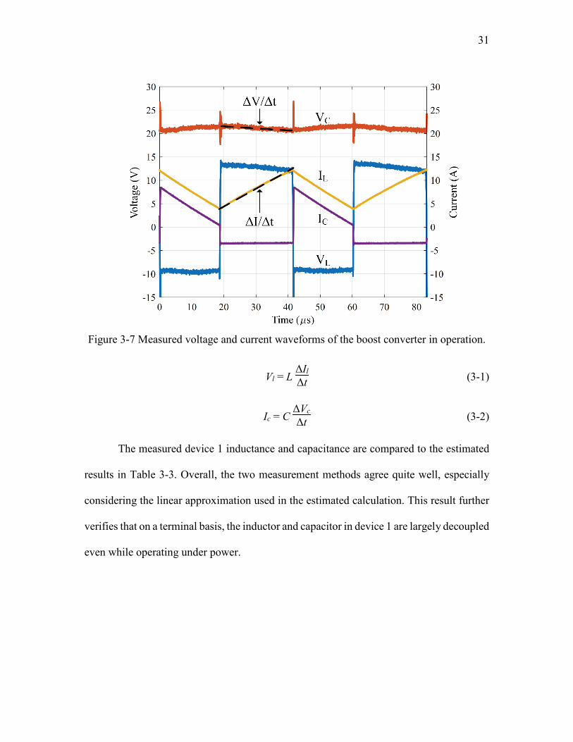
31
Figure 3-7 Measured voltage and current waveforms of the boost converter in operation.
Vl = L ΔIl
Δt (3-1)
Ic = C ΔVc
Δt (3-2)
The measured device 1 inductance and capacitance are compared to the estimated
results in Table 3-3. Overall, the two measurement methods agree quite well, especially
considering the linear approximation used in the estimated calculation. This result further
verifies that on a terminal basis, the inductor and capacitor in device 1 are largely decoupled
even while operating under power.

32
Table 3-3 Inductance and Capacitance of Device 1 in Operation
Estimated from Plot Measured Units
Inductance (L) 31 26 [μH]
Capacitance (C) 86 83 [μF]
In order to get a rough estimate of the losses in the boost converter while running
under load, a thermal image is shown in Figure 3-8. It is clear that the majority of the losses
in this converter are from hard switching of the MOSFET at 25 kHz, while the device 1
DEC is operating at about 11° C above the ambient temperature. Again, the goal is to
demonstrate decoupled operation of the DEC under load and show that no excessive
hysteresis or eddy current losses are present that do not otherwise occur in discrete devices.
The goal is not the performance or efficiency of a specific boost converter. Clearly, the
inductor and capacitor are not the main loss component in this converter, and the DEC is
operating well within its design temperature.
Figure 3-8 Thermal image of the boost converter at steady state under load.

33
3.4 Summary
• In this chapter, two different experimental prototypes were introduced. One
prototype has an air core and the other prototype includes magnetically permeable
material. Neither of the prototypes has been optimized and they are used to verify
the analytical model.
• The prototypes were evaluated to verify the analytical model by testing the
impedance versus frequency response of the individual inductor, individual
capacitor, as well as series and parallel connections of the inductor and capacitor
terminals. These experimental results of the series and parallel connection were
compared to analytical results of equivalent discrete components, and good
agreement between the two was found.
• One of the prototype devices was tested in a boost converter circuit, demonstrating
decoupled operation of the inductor and capacitor in the DEC under load. The boost
converter waveforms matched the classical waveforms expected from a circuit built
with discrete components, demonstrating decoupled operation in a power circuit,
without excessive loss components not already present in discrete devices.

34
Chapter 4: Integrated Device Design 4.1 Design Tradeoffs
When designing an integrated DEC inductor and capacitor for a specific
application, there are several tradeoffs involved. The tradeoffs examined here include the
thickness of the conductor material in the core, the design operating temperature, and the
parasitic equivalent series inductance seen at the capacitor terminals.
4.1.1 Conductor Thickness in Core
One of the parameters that can be adjusted in the design of a DEC device is the
thickness of the magnetically permeable material in the core. The two most common
realizations are either a thin metal foil or a metal vapor deposition layer applied directly to
the dielectric film. Figure 4-1 shows the tradeoff involved in changing the conductor
thickness if the core volume is held constant. While a thicker permeable conductor
increases the inductance of the core, it also simultaneously decreases the capacitance
because it displaces dielectric material from the constant volume core.
For the case where the permeable conductor material is vapor deposited onto the
dielectric film, the conductor will necessarily be thin relative to the dielectric thickness.
For this type of process, the device will tend to reside on the far left side of Figure 4-1,
where the conductor to insulator ratio is much less than 1. When a film-foil construction
method is used, the design will tend to be in the area of the figure where the ratio is greater
than 1. Therefore, the ratio of inductance to capacitance desired in the application will tend
to lead the designer towards a specific manufacturing process.

35
Figure 4-1 Inductance and capacitance versus premeable conductor thickness for a
constant core volume.
4.1.2 Temperature
Traditionally, film capacitors have been limited to applications where the capacitor
will not see a temperature over 100-125 °C depending on the choice of dielectric material.
Inductors, however, can be operated at much higher temperatures, often limited only by
the temperature rating of the wire insulation of the inductor winding. By incorporating
plastic dielectric films into the core of the device, the inductor operating temperature is
now limited by the dielectric material to a lower temperature than would otherwise be the
case if a standard inductor core were used. Clearly higher temperature dielectric films are
important for the full realization of the potential of this device. Specialty plastic films are
already available with slightly higher temperature ratings. In addition, flexible glass
dielectric films are also under development [18] and could potentially find use in this
application.
36
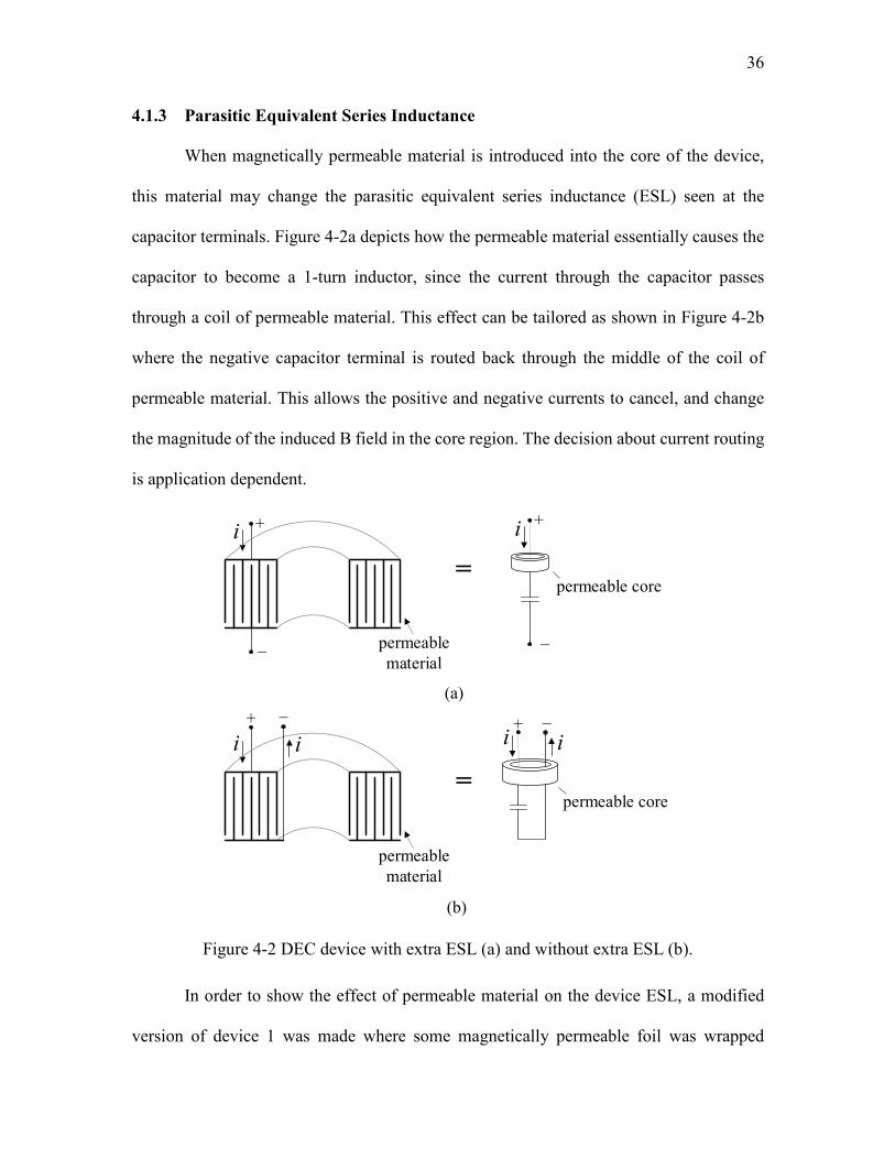
4.1.3 Parasitic Equivalent Series Inductance
When magnetically permeable material is introduced into the core of the device,
this material may change the parasitic equivalent series inductance (ESL) seen at the
capacitor terminals. Figure 4-2a depicts how the permeable material essentially causes the
capacitor to become a 1-turn inductor, since the current through the capacitor passes
through a coil of permeable material. This effect can be tailored as shown in Figure 4-2b
where the negative capacitor terminal is routed back through the middle of the coil of
permeable material. This allows the positive and negative currents to cancel, and change
the magnitude of the induced B field in the core region. The decision about current routing
is application dependent.
+
_
i +
_
i
permeable core
+ _
i+ _
i
permeable core
permeable material
permeable material
=
=
(a)
(b)
i i
Figure 4-2 DEC device with extra ESL (a) and without extra ESL (b).
In order to show the effect of permeable material on the device ESL, a modified
version of device 1 was made where some magnetically permeable foil was wrapped

37
around the outside of the same capacitor used in the core of device 1. This modified device
will be referred to as device 3. A view of device 3 with the inductor windings removed can
be seen in Figure 4-3 in order to illustrate the core topology. The inductor winding is then
wound around both the capacitor and the winding of permeable foil. In this design, the
electric field is in the capacitor, but a majority of the magnetic field is concentrated in the
metal foil that is wrapped outside the outer diameter of the capacitor. This device geometry
is an exaggerated version of the issue depicted in Figure 4-2 where the capacitor becomes
a 1-turn inductor as well as a capacitor.
Figure 4-3 View of device 3 core with inductor windings removed to show concentric electric field and magnetic field core arrangement.
The impedance versus frequency of this device as seen at the capacitor and inductor
terminals is shown in Figure 4-4. The inductance measurement was taken with the
capacitor terminals open circuited and the capacitance measurement was taken with the
inductor terminals open circuited. The inclusion of the magnetically permeable metal foil
in this topology affects the capacitor ESL, and the capacitor resonant frequency that was
at 70 kHz for device 1, is now at 20 kHz for device 3. It should be noted that the model for

38
the effective permeability of the core developed in section 2.3 does not apply to this device
since the fields are mostly not co-located.
Figure 4-4 Impedance vs. frequency of device 3 as seen at the inductor and capacitor
terminals.
The effects of negative capacitor terminal pass back are clearly apparent in
device 3. Since the magnetically permeable material in device 3 is located outside the outer
diameter of the capacitor, the entire capacitor current serves as a 1-turn inductor as the
current travels from the positive to the negative terminal. Figure 4-5 shows the impedance
versus frequency plot as seen at the device 3 capacitor terminals with and without the
negative terminal pass back cancellation method. Note that when the magnetic field outside
the capacitor outer diameter is cancelled by passing the negative terminal back through the
middle of the core, the self-resonant frequency of the capacitor increases due to the reduced
ESL as seen at the capacitor terminals.

39
Figure 4-5 Device 3 impedance vs frequency at the capacitor terminals with and without current loop cancellation.
4.2 Design Considerations
Since there are many variables the affect the ultimate inductance and capacitance
of the integrated device, design is not necessarily straightforward, especially when
designing for volume, weight, and/or cost minimization. This section presents
considerations for material selection and geometry selection that will ultimately affect the
total weight and volume of the device. This analysis assumes that the core consists of
spirally wound films in a toroidal geometry.
4.2.1 Material Selection
In the core, which is composed of alternating layers of conductor and dielectric
material wound in a spiral, the choice of the core materials greatly affects the performance
of the device. The conductor material conducts the capacitor current, as well as the
magnetic field generated by the inductor windings. Therefore, both the resistivity and
magnetic permeability of the conductor material are important properties. Figure 4-6 shows
the capacitor current conduction loss as a function of the conductor thickness for different

40
types of materials normalized to a 100 nm thick aluminum conductor. It should be noted
that changing the conductor material from aluminum to nickel without altering the core
geometry would result in an increase in capacitor conductor resistance of 2.46 times the
original resistance of the aluminum conductors. If this results in too much loss for the
capacitor, the conductor thickness can be increased slightly to offset the increased
resistivity. This increased thickness will also benefit the permeability of the core. Nickel
and cobalt are attractive options because their resistivity is not that much higher than
aluminum, and they provide magnetic permeability. Iron based materials may also be
attractive due to their higher permeability, but the tradeoff will be a higher capacitor ESR.
Figure 4-6 Comparison of normalized conduction loss for different conductor materials as a function of conductor thickness.
Table 4-1 gives the resistivity, permeability, and skin depth for the traditional
aluminum conductors as well as nickel, cobalt, and electrical steel, which are three different
possible conductors with increased magnetic permeability. Nickel and cobalt can be vapor
deposited directly onto the dielectric material, while nickel and steel can be drawn into thin

41
foils for film-foil capacitor construction. While electrical steel provides the best
permeability, it also has significantly higher electrical resistivity than aluminum. However,
since steel requires film foil construction, the increased resistance will be largely offset by
the greater material thickness. In addition, while nickel, cobalt, and electrical steel have
significantly reduced skin depth compared with aluminum, this disadvantage is offset by
the fact that the conductors used in film capacitor construction are typically thinner than
the skin depths listed in the table. Clearly, from a performance perspective, the choice of
conductor material depends on the application requirements for the inductor permeability
and the capacitor equivalent series resistance (ESR).
Table 4-1 Comparison of Core Conductor Materials
Al Ni Co Steel
Resistivity ρ [10-8 Ω∙m] 2.82 6.93 6.24 50
ρ / ρAl 1 2.46 2.21 17.73
Relative Permeability μr 1 600 250 4000
Skin Depth at 100 kHz [μm] 267 17 25 17.8
The dielectric material is also an important design consideration. Material
properties that affect capacitance such as relative permittivity and dissipation factor are
obviously important, as well as the maximum operating temperature of the film, since this
material is the thermally limiting factor in the design. Several common plastic films are
compared in Table 4-2: polyethylene terephthalate (PET), polyphenylene sulfide (PPS),
polyethylene naphtalate (PEN), and polypropylene (PP). PP and PET are probably the most
common, with PPS and PEN used in higher temperature applications, but typically at lower
volumes and higher prices. Other dielectric properties may also come into play depending
on the application.

42
Table 4-2 Comparison of Core Dielectric Materials
PET PPS PEN PP
Relative Permittivity εr 3.3 3.0 3.0 2.2
Max Application Temp [°C] 125 150 150 105
Dissipation Factor at 10 kHz 0.0110 0.0006 0.0070 0.0002
4.2.2 Geometry Selection
This integrated device can be fabricated in many different geometries. In addition
to the toroidal geometry already discussed at length, Figure 4-7 shows several different
possible geometric arrangements of the proposed integrated device. Figure 4-7a is a
sectioned view of the toroidal geometry that has already been discussed. Figure 4-7b shows
two spiral-wrapped DECs that have been arranged to form an E-core. Figure 4-7c shows a
DEC rolled in a solenoid shape with a solenoid inductor wrapped around it. Figure 4-7d
shows square-shaped DECs that have been cut in half to form C-cores. Note that the
orientation of the alternating layers can be either horizontal or vertical in this embodiment.
Finally, Figure 4-7e shows electric machine stator laminations where the dielectric material
serves as the insulating layer between each lamination. This design could be useful for
Integrated Modular Motor Drives (IMMD) where the drive electronics are integrated into
the machine itself [19], [20]. In this case, the dielectric layers between each lamination
could serve as the DC link capacitor.
The magnetic properties of the proposed designs are not all equivalent. In
Figure 4-7a and Figure 4-7b, the core constitutes a distributed air gap due to the spiral
winding. In these embodiments, the flux must cross the dielectric layer to make a complete
magnetic circuit. In Figure 4-7c-e, the flux does not have to cross the dielectric layer, and

43
as such, the flux will concentrate in the magnetically permeable material. In these designs,
the core is essentially a laminated core with a low fill factor. While magnetically different
than the core discussed in this thesis, these embodiments may still present unique
integration opportunities.
Figure 4-7 Concepts for possible integrated device geometries.
4.3 Design Procedure
The first step when designing an integrated device is to choose a dielectric material.
This choice is application dependent. The material permittivity must be weighed against
the voltage breakdown strength, maximum operating temperature, and dimensional
manufacturing limits. As discussed previously in Table 4-1, several different plastic films
are commonly used as dielectric materials in film-foil capacitors.
The second step is to choose the thickness of the dielectric material d1. Generally,
for dielectric materials, thinner is better, since that increases the capacitance. However, the

44
minimum manufacturing thickness as well as the voltage breakdown strength of the
material must be considered. The dielectric material must be thick enough to withstand the
peak voltage of the application, with sufficient margin for manufacturing variances as well
as transient over voltage conditions seen in the application.
The third step is to calculate the required capacitor “plate area” or dielectric width
times length w∙l to achieve the desired capacitance for the application. This is determined
by solving (2-1) for the plate area w∙l. The resulting equation is shown in (4-1). Now, after
choosing a desired core height h, (addressed next) which is typically greater than w due to
the end spray that shorts the foils, the winding length l can be calculated. Note that the air
gap thickness d2 is a function of the winding process, but it is typically very small.
wl =
d1
εr1 +
d2
εr2
2εo (4-1)
This capacitor design is now mostly specified. Some other considerations
concerning the capacitor are the equivalent series inductance (ESL) at the terminals and
the thermal properties of the capacitor, which affects its ability to dissipate heat. ESL is a
function of the geometry, and considerations for ESL minimization were discussed
previously. The thermal properties are dominated by the height of the core h, since most
heat is conducted axially out the top and bottom of the core by the capacitor conductors
and a smaller height allows for better cooling of the capacitor core [21].
The fourth step is to choose a DEC core inner diameter D1 and then calculate the
outer dimeter D2 based on the dielectric and conductor material dimensions. The geometry
is a spiral, but it is easy to approximate D2 of the DEC by using (4-2) which only has a
small error since the material thicknesses d and δ being thin compared to the coil diameter

45
D1. Note that core packaging may add a small amount to the core diameter and it may be
necessary to account for this in the calculations depending on the relative sizes of the core
and the packaging. The choice of the inner diameter D1 affects the number of inductor turns
that can be applied to the core, and must be big enough to allow for the number of inductor
turns required.
D2 ≈ 2( )d + δ + ( )D1 - 2( )d + δ 2 + 8( )d + δ l
π (4-2)
The fifth step is to calculate the number of turns required to get the necessary
inductance within the constraints of the fill factor of the core inner diameter D1. Given the
required inductance for the application and the dimensions of the core, the number of
required turns can be calculated by solving (2-2) for the number of turns N as shown in
(4-3). This is trivial when the core is made of plastic and aluminum, where μreff = 1.
N = 2πL
μreffμohln
D2
D1
(4-3)
When magnetically permeable material is included in the core, the average core
permeability μreff must be calculated first using (2-5). Note that the thickness of the
magnetically permeable material may be adjusted in order to tailor μreff to the application.
This will allow the inductance to be adjusted slightly. Note that significant changes to the
conductor thickness will require the outer diameter to be recalculated. There are limits to
this adjustment based on maximum and minimum thicknesses for both the film-foil and
vapor deposition manufacturing processes.
It is important to check the winding window fill factor using (4-4), given the
inductor wire cross sectional area A and the number of inductor turns N determined in (4-3).
Typically, the fill factor FF should be kept below 0.4 to allow for manufacturing feasibility.

46
FF = NA
π
D1
22 (4-4)
Tradeoffs in the inductor design include the inductor wire cross-sectional area A,
the core inner diameter D1, and the inclusion of magnetically permeable material in the
core. Increasing the wire cross-section will lower conduction losses, but will also decrease
the number of turns that can fit in a given core inner diameter, which will limit inductance.
The inductor wire cross-sectional area represents a tradeoff between efficiency and volume
minimization. In addition, changing the core inner diameter D1, will affect the number of
allowable inductor turns N. The inclusion of magnetically permeable material in the core
may introduce saturation issues depending on the topology and application requirements,
and adjusting the thickness of the permeable material will affect the amount of capacitance
achievable in a given core volume.
These five steps constitute a basic design overview for a toroidal geometry device
with a DEC. This analysis was specifically oriented towards a toroidal geometry with a
spirally wound film capacitor that serves as the inductor core.
4.4 Volume Minimization
One of the proposed advantages of this DEC device is that in addition to requiring
fewer manufacturing steps and materials it may be smaller than a discrete inductor and
capacitor placed side by side in certain applications. In order to ensure that this design uses
the minimum volume, the design can be iterated with different designer chosen variables.
Some variables are set by the design criteria. For example, the thickness of the
dielectric material in the core is determined by the required voltage rating of the capacitor.
However, some variables may be adjusted by the DEC designer, including the core height

47
h and the core inner diameter D1. In fact, these parameters have significant latitude for
adjustment in the design. However, it should be noted that increasing the core height h too
much will decrease the capacitor maximum current due to thermal limitations and
decreasing the inner diameter D1 too much will limit the number of inductor turns N that
fit in the core, thereby limiting the inductance.
Figure 4-8 shows the total volume of a DEC type device with the same design
parameters as device 1 as a function of the core height h and core inner diameter D1 which
are chosen by the designer. This volume was calculated by iterating through the design
procedure in section 4.3, and calculating the total volume for each geometry. The volume
includes the volume of the inductor windings around the core. Per the design procedure in
the previous section, the fill factor was checked at each iteration, and designs that violated
a maximum fill factor of 0.4 were not included in Figure 4-8. The MATLAB code used to
generate the plot is given in Appendix II.
By applying this volume minimization routine to device 1, it can be seen how much
smaller device 1 can be in the same application with the same inductance, capacitance, and
device ratings. The current core height h of device 1 is 36 mm and its current core inner
diameter D1 is 34.1 mm. Its measured volume including the inductor windings on the
outside of the core is about 87 mL. From Figure 4-8 the volume-minimized design for a
device with the same inductance, capacitance, and application ratings is with the designer-
chosen dimensions D1 = 17 mm and h = 38 mm.

48
Figure 4-8 DEC device volume when varying the core inner diameter D1 and the core height h.
Table 4-3 gives a comparison between the calculated volumes for the current device
1 dimensions and the volume-minimized dimensions. Note that the calculated volume of
85 mL matches closely with the actual device 1 volume of 87 mL. The updated design is
almost 46% smaller by volume than the original proof-of-concept prototype device. This
volume savings came primarily by making the core inner diameter D1 much smaller. The
two designs in Table 4-3 possess equivalent inductance and capacitance. This minimization
process is important since the passive inductors and capacitors are often the largest
components in power conversion systems.
00.06
0.05
0.06
0.1
Vol
ume
[L]
0.04 0.05
0.15
h [m]
0.04
D1 [m]
0.2
0.02 0.030.02
0 0.01

49
Table 4-3 Volume Comparison of Different Device 1 Designs
Device 1 Original Design
Device 1 Improved Units
D1 0.0341 0.017 [m]
h 0.036 0.038 [m]
Volume 0.085 0.046 [L]
In addition to volume minimization, weight and cost minimization may also be
desirable. A similar analysis and design procedure may be performed if weight is the most
critical attribute. If cost is the most important attribute, the design will be constrained by
which materials and geometries are the cheapest to acquire and manufacture, respectively.
These considerations will be different for every design and every application.
4.5 Manufacturing Considerations
As has been discussed previously, there are two primary methods for constructing
wound film capacitors: the film-foil design and the vapor deposition design. These two
manufacturing processes have been well developed for use with aluminum capacitor
conductors. However, the inclusion of magnetically permeable materials into the core may
have benefits for some applications requiring significant inductance, and manufacturing
considerations for achieving this are discussed here.
4.5.1 Vapor Deposition
Perhaps the most common method of manufacturing a film capacitor is to vapor-
deposit the aluminum conductor onto the plastic film. Then, two films that were metallized
using this process are rolled together to form the capacitor. Aluminum conductors are used
almost exclusively in this process in the film capacitor industry. It is possible to vapor-

50
deposit magnetically permeable nickel or nickel/cobalt alloys onto plastic film, and this
process was developed for the magnetic data-tape industry. However, this industry is nearly
obsolete, and most processing equipment has been mothballed or is currently in storage.
To get an idea of the bulk average magnetic permeability μreff available with this
manufacturing method, a roll of plastic film with a layer of nickel-cobalt vapor deposited
on one side was evaluated in the lab. The exact magnetic properties of the deposition layer
are unknown. The thickness of the vapor deposition is ~100 nanometers thick, and the
plastic film is ~12 micrometers thick, meaning that volumetrically, the core is > 99%
plastic.
The roll of material was wound with 32 turns of wire to form a toroidal inductor as
shown in Figure 4-9, and the inductance L of the winding was 21.5 µH. The dimensions of
the core were D1 = 152 mm, D2 = 217 mm, and h = 150 mm. The average permeability of
the core was estimated by solving equation (2-2) for μreff. The value of the inductance was
first adjusted to exclude the inductance contribution of the plastic bobbin in the center of
the roll of material that can be seen in Figure 4-9. In the case of this sample, the average
relative permeability of the core was 2.07.
Figure 4-9 Roll of plastic film with nickel-cobalt vapor deposition.

51
By adjusting the vapor deposition nickel percentage and the deposition thickness,
this average relative permeability could be adjusted. For practical designs the relative
permeability will likely remain below ~5 using the vapor deposition method due to the
limited thickness of vapor deposition, since applying a layer that is too thick will melt the
plastic film during processing.
4.5.2 Film-Foil
A second film capacitor manufacturing method is the film-foil construction
method. In this type of film capacitor, alternating layers of aluminum foil, which serve as
the capacitor conductors, and plastic film are rolled to form a capacitor. In this construction,
the metal conductors are much thicker (μm thickness vs nm thickness) than the vapor-
deposited conductors. These capacitors find use in high current applications since the
thicker conductors can carry more current, and are better at transmitting heat out to the
edges of the capacitor. The drawback is that these capacitors are much larger than their
vapor-deposited counterparts for the same capacitance rating.
Magnetically permeable metal foils are available in a variety of thicknesses
depending on the material, down to as thin as 1.75 micron thickness [22]. Examples of
magnetically permeable foils include electrical steel, pure nickel, and several nickel-iron
alloys such as Molypermalloy [23][24]. These types of metal foils have found use in
transformer, measurement, sensing and shielding applications, [22] but are not presently
used in the film capacitor manufacturing industry.
When producing a film-foil capacitor, the edge quality of the foil material is
extremely important. If there are any sharp edges or burrs on the metal foil, it can cut into
the plastic dielectric material and cause a short-circuit to the other metal foil, making the

52
capacitor useless. The sharp edge also makes it more difficult to process the foil material
since tears propagate quickly and can cause the foil to tear if the edge is already damaged
from previous processing. In this work, success was found with rotary knife slitting of
metal conductor materials in order to limit burrs on the metal edges.
While manufacturing processes have been refined for aluminum foil destined for
capacitor manufacturers, until now, there has not been a demand for magnetically
permeable metal foils for use in the capacitor manufacturing industry. Initial samples of
the nickel foil used to make prototypes contained sharp edges and burrs as shown in
Figure 4-10 that are not present in the aluminum foils used in the film capacitor industry.
These imperfections caused manufacturing issues because the nickel foil tore too easily in
the capacitor winding machines due to the imperfections.
Figure 4-10 Edge quality comparison of a sample of nickel foil to aluminum foil used in film capacitor manufacturing.
4.5.3 Reduced Manufacturing Processing
The proposed DEC device allows for production with fewer manufacturing steps
than manufacturing an independent inductor and capacitor. The manufacturing steps

53
required for construction are shown in Figure 4-11. As the figure indicates, the discrete
inductor core manufacturing processes shown in circles are eliminated since the capacitor
serves as the inductor core. This eliminates both manufacturing processes and raw
materials, which could save money. Obviously, the extent of any possible savings is
application dependent.
Figure 4-11 Manufacturing steps for discrete inductors and capacitors. The steps in circles can be eliminated with the integrated design.
4.6 Summary
• In this chapter, several different design tradeoffs involved in the design of toroidal
DEC devices were introduced. These tradeoffs include the thickness of the
conductor material in the core, the temperature limitations of the DEC and the
parasitic ESL that is a function of capacitor current routing. These tradeoffs are a
function of both materials and geometries.
• Several different design considerations were also introduced related to materials
and the geometry of the device. The benefits and drawbacks of several common

54
film capacitor dielectrics were discussed with properties of interest being
permittivity and maximum operating temperature. Several possible capacitor
conductor materials were also discussed, where it was noted that magnetically
permeable conductors have slightly worse electrical resistivity than aluminum. In
addition, implications for several possible geometries other than the toroidal
geometry were introduced.
• A systematic design procedure for specifying the device dimensions was
introduced. This design was then iterated by adjusting the size and shape of the core
parameters D1 and h, to determine the smallest possible volume for the design.
• Manufacturing considerations involved in adapting two different commercial film
capacitor winding processes for the DEC-type device were introduced and
discussed. Incorporating magnetically permeable material into the core via the
vapor deposition capacitor manufacturing process is possible, but expensive to
prototype and results in a relatively low μreff of the core. Incorporating magnetically
permeable material via the film-foil winding process much easier to prototype, but
very thin magnetically permeable materials are currently difficult to obtain due to
low manufacturing volumes.
• The DEC device can be made with only minimal modification of existing,
commercialized film capacitor manufacturing processes.

55
Chapter 5: Conclusion 5.1 Summary
A proposed inductor and capacitor integration method wherein the electric and
magnetic fields generated in the devices inhabit a common volume has been introduced.
This integration method involves winding an inductor winding around a film capacitor core
and utilizing the capacitor conductors as the magnetically permeable layers of the inductor
core. This concept was contrasted against other integration concepts, which integrated the
terminals of the devices and arranged the fields in close proximity instead of arranging the
electric and magnetic fields in a common volume.
An analytical model was presented that predicts the inductance and capacitance
seen at the terminals of the integrated device. This model accurately predicts L and C when
given the material properties and geometries. In addition, cross-coupling effects between
L and C were examined and it was shown that the inductor and capacitor terminals of the
device appear as decoupled, lumped elements. The effect of the inductor magnetic field on
the capacitor plate current distribution is minimal in practical designs; and the effect of the
magnetic field induced by the capacitor current that couples to the inductor winding is
minimal as long as the inductor amp-turn product is much larger than the capacitor current.
The analytical model was verified with experimental prototypes that show very
good correlation between the measured and modeled results, ultimately providing future
engineers a platform for design. A boost converter was constructed to demonstrate
decoupled operation of the DEC device L and C terminals under typical operating
conditions in a relevant power circuit.

56
Design tools and procedures were developed and presented in order to aid in
material property and geometry selection when designing an integrated device with volume
and weight minimization in mind. A systematic design procedure was developed to enable
methodical design of an integrated device of toroidal form factor. Then, the design
procedure was iterated to find the geometry that yielded the smallest volume. In addition,
considerations for manufacturing the core using the two most prevalent film capacitor
manufacturing methods were discussed.
5.2 Key Contributions
This thesis presents several contributions that extend on previous work. These
contributions are enumerated below.
1. A new method of integrating inductors and capacitors was introduced wherein the
capacitor plates of a rolled film capacitor are also utilized as the magnetically
permeable core of a separate inductor winding. This concept extends on previous
work by integrating the electric and magnetic fields in the DEC of the device while
still containing four terminals with the inductor and capacitor terminals
galvanically isolated. This allows the inductor and capacitor terminals to be
connected in series, in parallel, or individually in separate parts of the circuit.
2. An analytical model of the electric and magnetic fields in the core was developed
by deriving equations to calculate the inductance and capacitance as seen at the
device terminals. The inductance calculation was refined for the case where
magnetically permeable materials are included in the core of the device. In this
case, the equivalent core permeability was calculated by approximation of the spiral

57
winding as concentric magnetic circuits in parallel, providing an effective value of
the bulk core permeability.
3. Two different cross coupling mechanisms between the electric field and magnetic
field in the core were identified. The first mechanism is the effect of the magnetic
field caused by the capacitor current on the magnetic field that couples to the
inductor winding. This effect can be ignored when any appreciable number of
inductor turns is used around the core, since the inductor magnetic field will dwarf
the magnetic field induced by the capacitor. In the second coupling mechanism, the
magnetic field in the core induced by the inductor winding can influence the
capacitor current distribution on the capacitor ‘plates’. This effect is small enough
that it can be ignored, at least when using standard film capacitor conductors, which
are very thin compared to the skin depth.
4. Proof-of-concept (non-optimized) prototype devices were constructed for
experimental verification of the analytical model of the integrated device. The
prototype devices demonstrated decoupled operation on a small-signal and large-
signal basis both with and without magnetically permeable material in the core of
the device. The fidelity of the analytical model was further confirmed with testing
of an integrated device as the input inductor and output capacitor of a boost
converter.
5. Design and volume minimization guidelines were developed in order to understand
tradeoffs and material selection issues in the design. Capacitance is mainly
determined by dielectric thickness and material properties. Inductance is mainly
driven by the permeability of the conductor material in the core and the core size.

58
These considerations were incorporated into a systematic design procedure for
toroidal form factor devices.
6. A routine for volume minimization for toroidal form factor devices was proposed.
This routine was then used to minimize the volume of one of the prototype designs
in order to show how designer-chosen dimensions drive the overall volume of the
device and dictate possible volume savings.
5.3 Recommended Future Work
Through the course of this research, several areas of future work have been
identified and are listed below.
• Vapor deposition manufacturing technique
While the inclusion of magnetically permeable materials in the core of the device
has been demonstrated using the film-foil manufacturing technique, the inclusion of
permeable materials using the vapor deposition manufacturing technique may open up
additional applications for this integrated device with a DEC. Vapor deposition of
magnetically permeable material onto plastic films is technically possible and has been
demonstrated in other industries such as the magnetic data storage tape industry.
• Alternative device geometries
The analysis in this thesis focused on the toroidal geometry. Several other possible
geometries exist and may be the best choice for certain applications. These alternative
geometries include E-core and C-core DEC shapes with either spiral-wrapped or stacked
cores, spiral-wrapped cores in a solenoid inductor shape, and electric machine stator
lamination stacked geometries where the capacitor conductors become the laminations of
the electric machine.

59
• Weight minimization and cost optimization
While design for volume minimization has been explored here, minimizing weight
is often the most critical factor in aerospace applications, and optimizing cost is often the
most critical factor in consumer products. In these other cases, slightly different
optimization processes would be more appropriate and developing optimization procedures
for these cases would be beneficial.
• Loss Minimization
Designing for high efficiency and good thermal properties is an important
consideration in passive component design. Procedures and optimizations for these
considerations would be beneficial for designers.
• FEA Modeling
Although the analytical models proved to be accurate given the fine structure and
symmetry of the device, opportunities exist in FEA for modeling aspect ratios that no
longer lend themselves to straightforward analytical solutions. Due to the spiral geometry
and very thin material layers (micrometer-scale) in the core of the device, FEA modeling
of devices with any appreciable number of turns is not straightforward. Modeling
optimizations or appropriate simplifications could be investigated further to allow for more
robust prebuild verification of proposed designs.
• Filtering
Initial investigations indicate that several types of DEC devices would work well
as PWM output filters for inverters and dv/dt filters. Design and optimization for these or
other specific applications would be beneficial.

60
References [1] J. D. van Wyk and F. C. Lee, “On a Future for Power Electronics,” IEEE J. Emerg.
Sel. Top. Power Electron., vol. 1, no. 2, pp. 59–72, Jun. 2013.
[2] M. Marz, A. Schletz, B. Eckardt, S. Egelkraut, and H. Rauh, “Power electronics system integration for electric and hybrid vehicles,” in 2010 6th International Conference on Integrated Power Electronics Systems (CIPS), 2010, pp. 1–10.
[3] J. W. Kolar et al., “PWM Converter Power Density Barriers,” in 2007 Power Conversion Conference - Nagoya, 2007, p. P–9–P–29.
[4] R. Reeves, “Inductor-capacitor hybrid,” Proc. Inst. Electr. Eng., vol. 122, no. 11, pp. 1323–1326, Nov. 1975.
[5] J. Popovic-Gerber, M. Gerber, and B. Ferreira, “Integrated filter in electrolytic capacitor technology for implementation in high power density industrial drives,” in IEEE Power Electronics Specialists Conference, 2008. PESC 2008, 2008, pp. 2968–2974.
[6] C. Deng, M. Chen, P. Chen, C. Hu, W. Zhang, and D. Xu, “A PFC Converter With Novel Integration of Both the EMI Filter and Boost Inductor,” IEEE Trans. Power Electron., vol. 29, no. 9, pp. 4485–4489, Sep. 2014.
[7] S. J. Marais, J. A. Ferreira, and J. D. van Wyk, “Integrated filters for switch-mode power supplies,” in , Conference Record of the 1995 IEEE Industry Applications Conference, 1995. Thirtieth IAS Annual Meeting, IAS ’95, 1995, vol. 1, pp. 809–816 vol.1.
[8] R. Chen, S. Wang, J. D. van Wyk, and W. G. Odendaal, “Integration of EMI filter for distributed power system (DPS) front-end converter,” in Power Electronics Specialist Conference, 2003. PESC ’03. 2003 IEEE 34th Annual, 2003, vol. 1, pp. 296–300 vol.1.
[9] S. J. Marais, J. A. Ferreira, and J. D. van Wyk, “Planar integrated output filters for hybrids [SMPS],” in , 28th Annual IEEE Power Electronics Specialists Conference, 1997. PESC ’97 Record, 1997, vol. 2, pp. 1143–1149 vol.2.
[10] Y. Jiang, W. Liu, Y. Liang, J. D. van Wyk, and F. C. Lee, “A High-Power-Density Integrated Electronic Ballast for Low Wattage HID Lamps,” in APEC 2007 - Twenty Second Annual IEEE Applied Power Electronics Conference, 2007, pp. 274–280.

61
[11] Y. Jiang, F. C. Lee, J. D. van Wyk, J. D. van Wyk, Y. Liang, and W. Liu, “An Integrated Electronic Ballast for High Intensity Discharge (HID) Lamps,” in 2008 5th International Conference on Integrated Power Systems (CIPS), 2008, pp. 1–6.
[12] R. Chen, J. D. van Wyk, S. Wang, and W. G. Odendaal, “Improving the Characteristics of integrated EMI filters by embedded conductive Layers,” IEEE Trans. Power Electron., vol. 20, no. 3, pp. 611–619, May 2005.
[13] R. Chen, F. Canales, B. Yang, and J. D. van Wyk, “Volumetric optimal design of passive integrated power electronic module (IPEM) for distributed power system (DPS) front-end DC/DC converter,” in Industry Applications Conference, 2002. 37th IAS Annual Meeting. Conference Record of the, 2002, vol. 3, pp. 1758–1765 vol.3.
[14] C. P. Cho, W. A. Lynch, T. N. Ly, and R. A. McConnell, “Integrated capacitor and inductor,” U.S. Patent 7492240, 17-Feb-2009.
[15] D. Ludois, “Integrated capacitor and inductor having co-located magnetic and electrical energy storage volumes,” US9424984B2, 05-Mar-2014.
[16] A. Schroedermeier and D. C. Ludois, “An integrated inductor and capacitor with co-located electric and magnetic fields,” in 2015 IEEE Energy Conversion Congress and Exposition (ECCE), 2015, pp. 5293–5301.
[17] A. Schroedermeier and D. Ludois, “An Integrated Inductor and Capacitor with Co-Located Electric and Magnetic Fields,” IEEE Trans. Ind. Appl., Early Access. To appear in 2017.
[18] E. Furman and M. Lanagan, “High temperature dielectric materials and capacitors for transportation power electronics,” presented at the Applied Power Electronics Conference and Exposition (APEC) 2015.
[19] J. Wang, Y. Li, and Y. Han, “Evaluation and design for an integrated modular motor drive (IMMD) with GaN devices,” in 2013 IEEE Energy Conversion Congress and Exposition (ECCE), 2013, pp. 4318–4325.
[20] N. R. Brown, T. M. Jahns, and R. D. Lorenz, “Power Converter Design for an Integrated Modular Motor Drive,” in Conference Record of the 2007 IEEE Industry Applications Conference, 2007. 42nd IAS Annual Meeting, 2007, pp. 1322–1328.
[21] J. Bond, “The affects of capacitor geometries,” Electronic Concepts. [Online]. Available: http://www.ecicaps.com/wp-content/uploads/Affects-of-cap-geometries-Rev-A.pdf. [Accessed: 04-Jun-2015].

62
[22] “PTM Capabilities | Precision Rolled Thin & Ultra Thin Alloys.” [Online]. Available: http://www.arnoldmagnetics.com/precision-thin-metals/Capabilities. [Accessed: 06-Sep-2016].
[23] “Technical Literature | Ametek Hamilton Precision Metals.” [Online]. Available: http://www.hpmetals.com/technical-data.html. [Accessed: 06-Sep-2016].
[24] “Ultra-thin Metal | Specialty Rolled Metals | Rolled Alloys | Thin Foil.” [Online]. Available: http://www.arnoldmagnetics.com/precision-thin-metals/Materials/Materials-Overview. [Accessed: 06-Sep-2016].

63
Appendix I The equation for μr eff is approximately the same as the stacking factor formulation
given on the right hand side of (2-5). The algebraic manipulation and approximations used
to compare the two sides of (2-5) are detailed here.
Given (A-1) from the left side of (2-5) and multiplying the top and bottom by the
layer thickness δ + d, the equation now becomes (A-2).
µr eff = wh
( )δµrc+dµrd
∑i=1
nri
-1
ln
D2
D1
(A-1)
µr eff = wh
( )δµrc+dµrd
∑i=1
nri
-1
ln
D2
D1
( )δ + d( )δ + d (A-2)
It is easy to see that the sum of the circle radii ri multiplied by the layer thickness
δ + d approximates a natural logarithm of the ratio of the two core diameters D2 and D1 as
shown in (A-3) as long as δ + d is sufficiently small that the Riemann sum sufficiently
approximates the integral. The natural logarithms in the numerator and denominator cancel,
and the effective core permeability after the approximation in (A-3) is given in (A-4).
∑i=1
nri
-1 ( )δ + d ≈ ln
D2
D1 (A-3)
µr eff = wh
( )δµrc+dµrd
( )δ + d (A-4)

64
By separating terms and adding the term in parenthesis that evaluates to 0, the
equation becomes as shown in (A-5), and the terms can be regathered as in (A-6).
µr eff = wh
δ
δ+dµrc + dδ+dµrd +
δ
δ+dµrd - δδ+dµrd (A-5)
µr eff = wh
δ
δ+dµrc + δ+dδ+dµrd -
δδ+dµrd (A-6)
The definition of stacking factor, which is the ratio of the permeable material
thickness to the total layer thickness as shown in (A-7), can be substituted in and the
equation becomes as given in (A-8).
SF = δδ+d (A-7)
µr eff = wh [ ]SFµrc + ( )1 - SF µrd (A-8)
The result in (A-8) is the result on the right hand side of (2-5) and it represents a
simple approximation of the permeability of the core as long as the individual layers are
sufficiently thin that the integral approximation in (A-3) holds.

65
Appendix II This MATLAB code is for iteratively calculating the minimum volume of a specific
toroidal integrated inductor and capacitor design, using the design procedure specified in
Chapter 4.
% Integrated Inductor and Capacitor Volume Minimization % Andy Schroedermeier % 10 December 2016 % Volume minimization iterative routine by adjusting D1 and h % to get specified L & C. clc; clear variables; close all % Constants and Material Properties uo = 4*pi*0.0000001; % permeability of free space ur_film = 1; % permeability of dielectric material ur_cond = 1; % permeability of conductor material eo = 8.854e-12; % permittivity of free space er_film = 3.3; % permittivity of dielectric material er_gap = 1; % permittivity of air wire_dia = 0.001290; % inductor wire diameter (m) (16awg) % Design Capacitance and Inductance C = 0.000083; % Desired Capacitance (F) L = 0.000026; % Desired Inductance (H) % Design Parameters film_thick = 0.0000025; % dielectric film thickness (m) - Set by voltage rating gap_thick = 0.00000001; % air gap thickness (m) - Set by winding tension max_fill = 0.4; % maximum allowed core fill factor - set by winding process cond_thick = 0.00000005; % desired conductor thickness (m) % Design space core_id1 = 0.002:0.001:0.052; % core id (m) core_height1 = (0.002:0.001:0.052)'; % core height (m) core_id = repmat(core_id1,length(core_height1),1); core_height = repmat(core_height1,1,length(core_id1)); core_pad = 0.003; % additional padding for core casing (m) core_height_L = core_height+2*core_pad; % core height for inductor calcuations including casing % Calculate required wind length to get desired Capacitance wind_len = C*(film_thick/er_film+gap_thick/er_gap)./(2*eo*core_height);

66
% Calculate core_od from wind_len layer_thick = 2*(film_thick+cond_thick+gap_thick); roll_turns = (-pi*core_id+pi*layer_thick+sqrt((pi*core_id-pi*layer_thick).^2+4*pi*layer_thick*wind_len))/(2*pi*layer_thick); core_od = roll_turns*2*layer_thick+core_id+core_pad; % Find stacking factor (SF) and effective core permeability (ur_eff) SF = cond_thick/(cond_thick+film_thick+gap_thick); ur_eff = SF*ur_cond+1-SF; % Calculate # of inductor turns (N) needed to get L N = ceil(sqrt((2*pi*L)./(ur_eff*uo*core_height_L.*log(core_od./core_id)))); % Calculate core fill factor core_fill = (N*pi*(wire_dia/2)^2)./(pi*(core_id/2).^2); % Find total volume with center in liters including windings wire_top_thick = real((((1-sqrt(1-core_fill))/2).*core_id)/0.785); wire_od_thick = ((-core_od+sqrt(core_od.^2+core_fill.*core_id.^2))/2)/0.785; Volume=1000*pi*(core_height_L+2*wire_top_thick).*((core_od+2*wire_od_thick)/2).^2; % Remove entries with fill factor greater than max_fill for i=1:length(Volume(:,1)) for j=1:length(Volume(1,:)) if core_fill(i,j) > max_fill Volume(i,j) = NaN; end end end % Find and report minimum volume [min1,ind1] = min(Volume(:)); [m1,n1] = ind2sub(size(Volume),ind1); Total_Height_Min = core_height_L(m1,n1)+2*wire_top_thick(m1,n1); Total_OD_Min = core_od(m1,n1)+2*wire_od_thick(m1,n1); Core_Height_Min = core_height_L(m1,n1); Core_OD_Min = core_od(m1,n1); ID_Min = core_id(m1,n1); Volume_Min = Volume(m1,n1); N_min = N(m1,n1); % Get current volume (ID = 34mm H = 36 mm) Volume_Current = Volume(33,35); % Plot volume versus core id and height figure(1) surf(core_id(1,:), core_height_L(:,1), Volume,'EdgeColor','none') set(gca,'fontsize',16,'FontName','Times New Roman') xlabel('D1 [m]') ylabel('h [m]') zlabel('Volume [L]')

67
% Print Results x1 = (['Core height at min volume: ',num2str(Core_Height_Min),' [m]']); x2 = (['Core OD at min volume: ',num2str(Core_OD_Min),' [m]']); x3 = (['ID at min volume: ',num2str(ID_Min),' [m]']); x4 = (['Minimum Volume: ',num2str(Volume_Min),' [L]']); x5 = (['Current Volume (calc): ',num2str(Volume_Current),' [L]']); disp(' '); disp(x1); disp(x2); disp(x3); disp(x4); disp(x5); disp(' ');


![Capacitors and Inductors [Compatibility Mode]](https://static.fdocuments.in/doc/165x107/546a9ac3b4af9fe5268b47da/capacitors-and-inductors-compatibility-mode.jpg)