Integrated color pixels in 0.18-mm complementary metal
14
Integrated color pixels in 0.18-mm complementary metal oxide semiconductor technology Peter B. Catrysse and Brian A. Wandell Department of Electrical Engineering, Stanford University, Stanford, California 94305 Received January 14, 2003; revised manuscript received June 11, 2003; accepted July 23, 2003 Following the trend of increased integration in complementary metal oxide semiconductor (CMOS) image sen- sors, we have explored the potential of implementing light filters by using patterned metal layers placed on top of each pixel’s photodetector. To demonstrate wavelength selectivity, we designed and prototyped integrated color pixels in a standard 0.18-mm CMOS technology. Transmittance of several one-dimensional (1D) and two- dimensional (2D) patterned metal layers was measured under various illumination conditions and found to exhibit wavelength selectivity in the visible range. We performed (a) wave optics simulations to predict the spectral responsivity of an uncovered reference pixel and (b) numerical electromagnetic simulations with a 2D finite-difference time-domain method to predict transmittances through 1D patterned metal layers. We found good agreement in both cases. Finally, we used simulations to predict the transmittance for more elaborate designs. © 2003 Optical Society of America OCIS codes: 040.6040, 050.2770, 110.2970, 130.3120, 130.5990, 230.3990. 1. INTRODUCTION Digital cameras have emerged as the dominant image- capture technology. The core component of a digital cam- era, its image sensor, records an optical image as a spa- tially sampled array of pixels. The charge accumulated in these pixels is an approximately linear representation of the local image irradiance. To create color images, color filters are inserted in the optical path before each pixel; these filters control the likelihood that various wavelengths will be transmitted to each pixel and its pho- todetector. Color filters are commonly superimposed on the image sensor during independent steps in the manu- facturing process. 1,2 An important trend in digital camera design is the de- velopment of complementary metal oxide semiconductor (CMOS) image sensors. These sensors are being scaled with CMOS technology to make possible an increasing level of integration of capture and processing to reduce system power and cost. 3 Toward completing design inte- gration of color image sensors in CMOS technology, we have explored the possibility of introducing wavelength selectivity with only standard processing steps, i.e., with- out inserting a color filter. Specifically, we have imple- mented filters that consist of patterned metal layers placed within each pixel to control the transmission of light through the pixel to its photodetector. We refer to such pixel design as an integrated color pixel (ICP). ICPs may be useful for digital camera applications but may be even more suited to multispectral imaging and a variety of other image-sensing applications. We demonstrated the first ICPs featuring visible wave- length selectivity by using subvisible-wavelength pat- terned metal layers in a standard 0.18-mm CMOS technology. 4 Here we describe the comprehensive optical characterization of CMOS ICPs, including transmittance measurements under various illumination conditions. We also present what is to our knowledge the first model to characterize (a) the optical path from the pixel surface to the photodetector in a CMOS image sensor and (b) the effect of placing patterned metal layers in this path. We compare the measured and the predicted transmittances, and then we show, by simulation, examples of additional transmittances that can be achieved by using advanced CMOS technologies and multiple patterned metal layers simultaneously. 2. BACKGROUND A. Color Filter Arrays Today the main method of implementing color image sen- sors for digital cameras is the color filter array 5 (CFA). The CFA consists of a color filter pattern, comprising a regular array of filters with several different wavelength transmittances, that is deposited onto the monochrome pixels to separate out the wavelengths of incident light. In one common form, this architecture uses a spatial pat- tern comprising three red – green– blue (RGB) interleaved color mosaics. 6,7 An alternative pattern, often used for video capture, comprises an array of four cyan– magenta – yellow– green (CMYG) color filters. 8 The CFA color architecture has been quite successful for CCD imagers, but it does have several performance drawbacks when applied to CMOS image sensors. First, the CFA is applied to the pixel surface, whereas the pho- todetector is located in the substrate [Fig. 1(a)]. In 0.18-mm CMOS technology, the distance between filter and detector can be as much as 10 mm for a typical 6-mm pixel with a 3-mm photodetector. This spacing makes the pixel a less efficient light collector than it could be. 9 It also permits light intended for, say, the red photodetector to refract or scatter and arrive, instead, at a neighboring blue photodetector. This phenomenon is called color cross talk. 10,11 Further, the relatively large separation imposes stringent design constraints on micro- P. B. Catrysse and B.A. Wandell Vol. 20, No. 12/December 2003/J. Opt. Soc. Am. A 2293 1084-7529/2003/122293-14$15.00 © 2003 Optical Society of America
Transcript of Integrated color pixels in 0.18-mm complementary metal

P. B. Catrysse and B. A. Wandell Vol. 20, No. 12 /December 2003 /J. Opt. Soc. Am. A 2293
Integrated color pixels in 0.18-mm complementarymetal oxide semiconductor technology
Peter B. Catrysse and Brian A. Wandell
Department of Electrical Engineering, Stanford University, Stanford, California 94305
Received January 14, 2003; revised manuscript received June 11, 2003; accepted July 23, 2003
Following the trend of increased integration in complementary metal oxide semiconductor (CMOS) image sen-sors, we have explored the potential of implementing light filters by using patterned metal layers placed on topof each pixel’s photodetector. To demonstrate wavelength selectivity, we designed and prototyped integratedcolor pixels in a standard 0.18-mm CMOS technology. Transmittance of several one-dimensional (1D) and two-dimensional (2D) patterned metal layers was measured under various illumination conditions and found toexhibit wavelength selectivity in the visible range. We performed (a) wave optics simulations to predict thespectral responsivity of an uncovered reference pixel and (b) numerical electromagnetic simulations with a 2Dfinite-difference time-domain method to predict transmittances through 1D patterned metal layers. We foundgood agreement in both cases. Finally, we used simulations to predict the transmittance for more elaboratedesigns. © 2003 Optical Society of America
OCIS codes: 040.6040, 050.2770, 110.2970, 130.3120, 130.5990, 230.3990.
1. INTRODUCTIONDigital cameras have emerged as the dominant image-capture technology. The core component of a digital cam-era, its image sensor, records an optical image as a spa-tially sampled array of pixels. The charge accumulatedin these pixels is an approximately linear representationof the local image irradiance. To create color images,color filters are inserted in the optical path before eachpixel; these filters control the likelihood that variouswavelengths will be transmitted to each pixel and its pho-todetector. Color filters are commonly superimposed onthe image sensor during independent steps in the manu-facturing process.1,2
An important trend in digital camera design is the de-velopment of complementary metal oxide semiconductor(CMOS) image sensors. These sensors are being scaledwith CMOS technology to make possible an increasinglevel of integration of capture and processing to reducesystem power and cost.3 Toward completing design inte-gration of color image sensors in CMOS technology, wehave explored the possibility of introducing wavelengthselectivity with only standard processing steps, i.e., with-out inserting a color filter. Specifically, we have imple-mented filters that consist of patterned metal layersplaced within each pixel to control the transmission oflight through the pixel to its photodetector. We refer tosuch pixel design as an integrated color pixel (ICP).ICPs may be useful for digital camera applications butmay be even more suited to multispectral imaging and avariety of other image-sensing applications.
We demonstrated the first ICPs featuring visible wave-length selectivity by using subvisible-wavelength pat-terned metal layers in a standard 0.18-mm CMOStechnology.4 Here we describe the comprehensive opticalcharacterization of CMOS ICPs, including transmittancemeasurements under various illumination conditions.We also present what is to our knowledge the first model
1084-7529/2003/122293-14$15.00 ©
to characterize (a) the optical path from the pixel surfaceto the photodetector in a CMOS image sensor and (b) theeffect of placing patterned metal layers in this path. Wecompare the measured and the predicted transmittances,and then we show, by simulation, examples of additionaltransmittances that can be achieved by using advancedCMOS technologies and multiple patterned metal layerssimultaneously.
2. BACKGROUNDA. Color Filter ArraysToday the main method of implementing color image sen-sors for digital cameras is the color filter array5 (CFA).The CFA consists of a color filter pattern, comprising aregular array of filters with several different wavelengthtransmittances, that is deposited onto the monochromepixels to separate out the wavelengths of incident light.In one common form, this architecture uses a spatial pat-tern comprising three red–green–blue (RGB) interleavedcolor mosaics.6,7 An alternative pattern, often used forvideo capture, comprises an array of four cyan–magenta–yellow–green (CMYG) color filters.8
The CFA color architecture has been quite successfulfor CCD imagers, but it does have several performancedrawbacks when applied to CMOS image sensors. First,the CFA is applied to the pixel surface, whereas the pho-todetector is located in the substrate [Fig. 1(a)]. In0.18-mm CMOS technology, the distance between filterand detector can be as much as 10 mm for a typical 6-mmpixel with a 3-mm photodetector. This spacing makes thepixel a less efficient light collector than it could be.9 Italso permits light intended for, say, the red photodetectorto refract or scatter and arrive, instead, at a neighboringblue photodetector. This phenomenon is called colorcross talk.10,11 Further, the relatively large separationimposes stringent design constraints on micro-
2003 Optical Society of America

2294 J. Opt. Soc. Am. A/Vol. 20, No. 12 /December 2003 P. B. Catrysse and B. A. Wandell
lenses; these constraints are usually necessary to increasethe sensitivity of CMOS image sensor pixels.12
There are several designs that aim to alleviate theproblems with the CFA architecture. For example,single-chip three-colors-in-one-pixel CMOS image-sensordesigns have emerged. The thin-film-on-application-specific integrated circuit (ASIC) (TFA) approach depositsthin-film detectors with adjustable spectral sensitivity ontop of an ASIC.13 In a second approach, a triple-wellstructure is used to exploit silicon’s differences in the ab-sorption length of light of different wavelengths for colorseparation.14 Although promising, neither of these re-cent designs can be easily implemented in a standardCMOS process without making significant modificationsin the process.
Fig. 1. Geometry of four pixels in a CMOS image sensor. (a) Aconventional arrangement including a RGB color-filter arrayplaced on the sensor surface. (b) The integrated color pixel ar-rangement that contains patterned metal layers (shown in color)within the pixel tunnels. Used by permission of the copyrightholder, R. Motta.
B. Wire GridsThe use of wire grids for filtering electromagnetic radia-tion goes back to the early experiments of Heinrich Hertzin the late 1800s.15 In the field of microwave engineer-ing, regular metal grids have been used for a long time asfilters, transmitting some wavelengths and blockingothers.16 More recently, as a result of continued ad-vances in the manufacturing technology of integrated-circuits, metal grids with periodicity commensurate withthe wavelength of near-infrared light have beendemonstrated,17 and some of their properties have beenstudied numerically. For example, Jensen and Nordindescribe a numerical electromagnetic study of the trans-mission characteristics of finite-aperture wire-gridpolarizers.18
Integrating the light filters, with use of patternedmetal layers, inside image sensor pixels offers several po-tential advances. Placing the light filters close to thephotodetector reduces color cross talk, and pixel vignett-ing and increases the efficiency of microlenses because ofthe smaller distance from pixel surface to pixel photode-tector. By controlling wavelength responsivity in thepixel design process, ICPs eliminate the need for addi-tional CFA manufacturing steps. The patterns used inthe design of an ICP use already available metal layersand are deposited on top of the photodetector in a CMOSimage-sensor pixel.
Why have wire grids not been used for color filtering inthe visible light regime? To control light in the visiblewavelength range requires periodicities smaller than thevisible range. This has been impossible until very recent0.18-mm CMOS technologies were used to make imagesensors. Even with the wire sizes possible in 0.18-mmCMOS technology, which is considered state of the art forimage sensors, we are on the edge of controlling visiblewavelengths. Nevertheless, as CMOS technologies keepscaling and smaller feature sizes become possible, CMOSimage sensors are bound to become viable in these moreadvanced technologies.
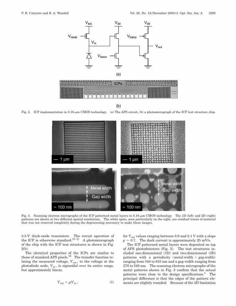
3. IMPLEMENTATION: INTEGRATEDCOLOR PIXEL TEST STRUCTURESWe designed and implemented ICP test structures in astandard 0.18-mm CMOS technology to demonstrate thevisible wavelength selectivity of patterned metal layersand to investigate their use for color imaging [Fig. 1(b)].Periodic patterns were created in the metal layers al-ready present in the process. These patterns comprisedan array of elements whose gap widths ranged from 270to 540 nm. The refractive index of the surrounding di-electric is 1.46. In air the visible wavelength regime isroughly from 400 to 750 nm; in this medium the effectivevisible wavelength regime is roughly from 270 to 510 nm.
We implemented test structures comprising 12-mmICPs with n-diffusion/p-substrate (n 1 /psub) photo-diodes. An ICP circuit schematic is shown in Fig. 2(a).A standard three-transistor active-pixel-sensor (APS) cir-cuit, directly connected to a chip output via a two-stagefollower amplifier, was used. Transistor gate leakagewas reduced, and voltage swing was increased, by using
P. B. Catrysse and B. A. Wandell Vol. 20, No. 12 /December 2003 /J. Opt. Soc. Am. A 2295
Fig. 2. ICP implementation in 0.18-mm CMOS technology. (a) The APS circuit, (b) a photomicrograph of the ICP test structure chip.
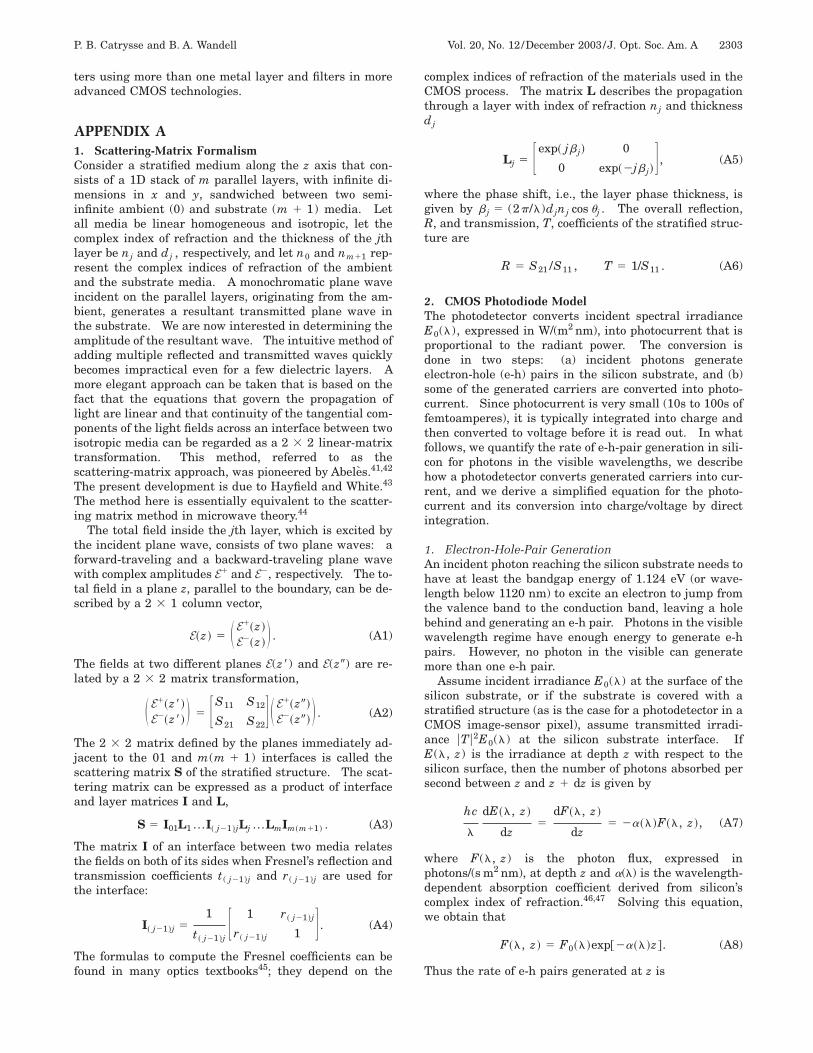
Fig. 3. Scanning electron micrographs of the ICP patterned metal layers in 0.18-mm CMOS technology. The 1D (left) and 2D (right)patterns are shown at two different spatial resolutions. The white spots, seen particularly on the right, are residual traces of materialthat was not removed completely during the deprocessing necessary to make these images.
3.3-V thick-oxide transistors. The circuit operation ofthe ICP is otherwise standard.19–21 A photomicrographof the chip with the ICP test structures is shown in Fig.2(b).
The electrical properties of the ICPs are similar tothose of standard APS pixels.19 The transfer function re-lating the measured voltage, Vout , to the voltage at thephotodiode node, V in , is sigmoidal over its entire range,but approximately linear,
Vout 5 gV in , (1)
for Vout values ranging between 0.9 and 2.1 V with a slopeg 5 0.7. The dark current is approximately 25 mV/s.
The ICP patterned metal layers were deposited on topof APS photodetectors (Fig. 3). The test structures in-cluded one-dimensional (1D) and two-dimensional (2D)patterns with a periodicity (metal width 1 gap width)ranging from 540 to 810 nm and a gap width ranging from270 to 540 nm. The scanning electron micrographs of themetal patterns shown in Fig. 3 confirm that the actualpatterns were close to the design specifications.4 Theprincipal difference is that the edges of the pattern ele-ments are slightly rounded. Because of the 2D limitation

2296 J. Opt. Soc. Am. A/Vol. 20, No. 12 /December 2003 P. B. Catrysse and B. A. Wandell
of the current generation of finite-difference time-domainsimulation software,22 we are able to simulate only the1D patterned metal layers. Hence we focus our discus-sion on these arrays and the associated simulation predic-tions.
4. EXPERIMENTAL METHODSICP characterization includes optical and electricalmeasurements.21,23,24 To measure the ICP characteris-tics accurately, one has to take special care to minimizethe environmental interferences such as electromagneticinterference and light source and temperature fluctua-tions. We housed the setup in an air-conditioned darkroom on an optical tabletop. All identifiable sources ofstray light were blocked, and experiments were per-formed remotely by use of a networked computer inter-face. Temperature was kept close to 25 °C. Absolute ir-radiance E(l) of the light source in W/(m2 nm) wasmeasured with a spectroradiometer and a diffuse whitestandard. Calibration measurements were repeated dur-ing each experimental series.
A. Electrical SetupThe electrical setup consists of a device-under-test board,a power supply, an analog output board, and a data acqui-sition board. All electrical equipments are computer con-trolled.
The device-under-test board holds the ICP test chip,some analog bias circuits, and a digital control signal in-terface. The board is mounted on an XYZ-translationstage, which in turn is placed on a rotation stage. Theboard and chip are aligned with the monochromator out-put port by use of an optical rail.
A highly regulated dc power supply is used to provide astable Vdd 5 3.3 V with less than 2 mV of ripple (peak topeak) for the entire chip. The analog output board pro-vides the two bias voltages Vbiasn and Vbiasp for the two-stage follower that converts the ICP response to the out-put, the reset voltage level Vset for the ICP photodiode,and the reset pulse Vreset , which determines the integra-tion time. All these analog output waveforms are gener-ated with a 12-bit resolution at a 1-MHz rate. The ana-log output board also provides the digital control signalfor the 5-bit multiplexer, which is used to select one of the32 pixels by connecting the multiplexer output node to theglobal output pad of the chip. The data acquisition boardsamples and digitizes the analog voltage signal at the ICPoutput at a 1-kHz rate, using a 12-bit analog-to-digitalconverter. The analog/digital range from 0 to 5 Vmatches the ICP output signal range. The output rangespans 0.9 to 2.0 V with quantization steps of 1.22 mV.The 1-kHz sampling rate is sufficiently fine to capture in-tegration times ranging from 75 ms to 2 s.
B. Optical SetupThe optical setup comprises a quartz–tungsten halogenlight source, a fiber light guide, a monochromator, an in-tegrating sphere, a collimator–polarizer, and a spectro-radiometer.
A dc-regulated light source with a 150-W quartz–tungsten halogen lamp provides stable optical power out-
put from 400 to 1100 nm with less than 0.1% short-termripple and noise (intra-experiment stability) and less than1% long-term drift (inter-experiment stability). Amatched fused-silica fiber light guide delivers the light tothe input port of a monochromator with an approximateefficiency of 50% for the entire wavelength range.
An 1/8-m motorized monochromator, based on an out-of-plane Ebert–Fastie design, separates the broadbandwhite-light input into narrowband spectral componentsby using a 1200-l/mm ruled grating with a 350-nm blazewavelength. Its peak efficiency is 80% at 400 nm, and itsprimary wavelength region is from 200 to 1600 nm(efficiency . 20%). To control the spectral resolution ofthe light at the output port, we use fixed input and outputslits with different widths. The slit width controls thespectral resolution (the narrower the slit, the smaller thewavelength band of the light source selected at the outputport) and simultaneously the amount of light transmitted.We used slits with resolution at 500 nm ranging from 1 to10 nm. Most of the measurements were done with afixed slit that provided an 8-nm FWHM passband. Thisslit passes enough light that the photocurrent exceeds thedark current by at least a factor of 2 across measurementwavelengths. The passband also limits the wavelength-sampling interval to exceed 8 nm, which is adequate forcharacterizing the expected transmittance of the pat-terned metal layers.
The output of the monochromator can be connected toan integrating sphere to provide a uniform, randomly po-larized illumination. This is useful for emulating imag-ing conditions. We used a 2-in. integrating sphere spe-cifically designed for uniform monochromatorillumination. It has excellent diffusing properties pro-vided by a very stable barium-sulfate-based white coat-ing, which is .95% reflective from 400 to 700 nm.Proper baffling prevents ‘‘first-strike’’ radiation from en-tering the instrument. Alternatively, the output of themonochromator can be connected to a collimator–polarizer to provide a collimated, linearly polarized illu-mination. This is most useful for performing analysismeasurements, i.e., measurements with simple illumina-tion conditions that can be either analytically or numeri-cally simulated.
The spectroradiometer is used to make absolute irradi-ance measurements of the light incident on the ICP. Thespectroradiometer measures the spectral radiance from380 to 780 nm with a spectral bandwidth of 8 nm and anaccuracy of 2 nm. To allow irradiance measurements, weaim the spectroradiometer at a diffuse white standard.The white standard has reflectance values ranging from95% to 99% for the visible (61%) and near-infrared (64%)spectrum and is highly Lambertian over its effective spec-tral range. This enables us to use a simple conversionformula to calculate the incident irradiance E(l), inW/(m2 nm), at the location of the patch from the measuredradiance L(l), in W/(m2 nm sr), re-emitted by the patch,
E~l! 5 pL~l!. (2)
The RS-232 serial port of a networked computer controlsboth the monochromator and the spectroradiometer.

P. B. Catrysse and B. A. Wandell Vol. 20, No. 12 /December 2003 /J. Opt. Soc. Am. A 2297
C. Transmittance MeasurementIf a photodiode is exposed to a narrowband spectral irra-diance E(l), the collected photo charge Q can be ex-pressed as
Q 5 Aeff T intE SR~l!E~l!dl ' Aeff T int SR~l!E~l!Dl,
(3)
where Aeff is the effective photodetector area of a pixel,T int is the integration time, and SR(l) is the spectral re-sponsivity in A/W.25 The collected charge Q is propor-tional to the voltage V in at the photodiode node [see Fig.2(a)],
V in 5Q
C int'
Aeff T int
C intSR~l!E~l!Dl. (4)
Hence, within the linear regime of the transfer functionEq. (1), the spectral responsivity SR(l) is proportional tothe measured voltage Vout at the multiplexer output node
Fig. 4. Spectral responsivity of an uncovered pixel (circles con-nected by solid lines) measured with unpolarized narrowband il-lumination (10-nm sampling intervals, FWHM of 8 nm). (a) Thesolid curve is the predicted spectral responsivity, based on thescattering-matrix (SM) calculations derived in Subsection 6A.The error bar shows a typical 1 standard deviation for the mea-surements. (b) The geometry of the pixel assumed in calculat-ing the 1D scattering-matrix model is shown.
divided by the input narrowband spectral irradiance E(l)at the input wavelength,
SR~l! 'C int
Aeff T int
Vout
g
1
E~l!Dl. (5)
The spectral responsivity SR(l) of the uncovered pixel,measured with a collimated source, is shown by thecircles connected by solid lines in Fig. 4. The spectral re-sponsivity is typical for the silicon substrate in a CMOSprocess.26 It starts out low, near 400 nm, owing to reflec-tion and absorption in the stratified structure precedingthe pn-junction photodiode. It peaks near 600 nm as aresult of the location of the pn junction 200 nm below thesilicon surface. It falls off at higher wavelengths, and fi-nally silicon becomes transparent for wavelengths largerthan 1120 nm, which corresponds to its bandgap. Wewill compare these measurements with theory in more de-tail in Section 6. The predicted rapid oscillations arisebecause of Fabry–Perot resonance behavior within thepixel structure. These oscillations are frequently foundwhen one is measuring at a fine enough wavelength reso-lution (,10 nm) using collimated sources. More typi-cally, however, SR(l) is measured by using wide-angle,unpolarized illumination from an integrating sphere.Such light masks most of the Fabry–Perot resonance be-havior. The spectral transmittance through the pat-terned metal layers is measured indirectly by comparingthe spectral responsivity of the ICP with that of an uncov-ered reference pixel,
Tmeas~l! 5SRICP~l!
SRRef ~l!. (6)
5. EXPERIMENTAL RESULTSFigure 5 shows the spectral transmittance of a 1D pat-terned metal layer consisting of 270-nm-wide wires andgap widths ranging from 270 to 540 nm, where sizes rep-resent the design specifications. Transmittance is shownfor collimated illumination polarized with the electricfield parallel to the wires [TE; Fig. 5(a)] and with the elec-tric field perpendicular to the wires [TM; Fig. 5(b)].
Although we refer to the measurement conditions asTE and TM, the 1D patterned metal layers are parallelwires whose edges do not quite connect to the metalshield (see Fig. 3, left side). These edges form two verti-cal gaps perpendicular to the main polarization direction.Consequently, the measurements are TE or TM weightedrather than pure TE or TM measurements.
Both TE and TM transmittance behavior is determinedby both pattern geometry and material properties. Spe-cifically, we have observed two TE transmittance regions:a constant but attenuated transmission region (left) and acutoff region (right). We summarize the behavior inthese regimes with a three-parameter model consisting ofa constant transmittance level a, a cutoff wavelengthlcutoff , and a cutoff rate b:
T 5 H a l < lcutoff
a 2 b~l 2 lcutoff! l . lcutoff. (7)

2298 J. Opt. Soc. Am. A/Vol. 20, No. 12 /December 2003 P. B. Catrysse and B. A. Wandell
The parameters in this empirical model can be related tothe geometrical properties of the grating, as we describelater.
The empirical model for the TE measurements showsthat for the three pixels in Fig. 5(a), the lcutoff value in-creases with gap width (677, 750, and 875 nm). Thetransmittance level a increases with increasing gap–metal ratio (0.41, 0.47, and 0.50). The small discrepan-cies between a and the gap–metal ratio are probably dueto a variety of minor factors, such as incomplete periodsat the photodetector margin and absorption of the wirematerial (400-nm aluminum core with a 25-nm coating oftitanium nitride on both top and bottom surfaces). Thecutoff rate b is roughly the same at 0.001 nm21. Its ac-curate calculation is impeded by the rapid oscillations,which coincide with location of the cutoff wavelength.
The TM transmittances in Fig. 5(b) differ in a few waysfrom the TE transmittances. Mainly, the transmittancein the lower wavelength regime deviates significantlyfrom the constant level expected by the gap–metal ratio.The TM transmittance measurements do decline atlonger wavelengths, similar to the falloff in the TE case,but there are some differences. The most notable differ-ence is that the falloff is steeper in TM than in TE mea-surements.
Fig. 5. Measured transmittance of 1D ICPs with gap widths de-signed to be 270 (circles), 360 (triangles), and 450 (squares) nm.Measurements are shown for collimated, polarized illumination:(a) electric field parallel with wires (TE) and (b) electric field per-pendicular to wires (TM).
The transmittance measurements with wide-angle, un-polarized illumination (Fig. 6) can be explained on the ba-sis of the linearity of the transmitted light; i.e., the wide-angle, unpolarized results are a weighted sum of thesingle-angle collimated illumination at each polarization.Even under these more natural imaging conditions,changing the gap width changes the spectral transmit-tance of the patterned metal layers.
The pixel spectral responsivity obtained by using planewaves (collimated, polarized illumination) has rapid oscil-lations [see Fig. 4(a)]. These oscillations are also plainlyvisible in the transmittance measurements of the pat-terned metal layers in regions near 600–700 nm [Figs.5(a) and 5(b)]. The oscillations are greatly reduced whenmeasuring is with incident waves spanning many angles,say, when an integrating sphere is used. As we describein Section 6, the position and spacing of these oscillationscan be understood as caused by Fabry–Perot reflectionsbetween the silicon nitride (Si3N4) and silicon dioxide(SiO2) layers in the pixel. The introduction of the pat-terned metal layer further subdivides the pixel cavity andintroduces additional reflections. Hence some of theseoscillations are visible in the transmittance measure-ments.
6. THEORYThe key properties of the experimental data include (a)the spectral responsivity of the uncovered reference pixeland (b) the transmittance of the patterned metal layers inthe ICP. In this section we show that both of these prop-erties can be predicted. The reference pixel responsivitycan be predicted with an analytical model based on ascattering-matrix approach and a model of the photodi-ode. The measured TE and TM transmittance of the pat-terned metal layers can be predicted by using a numericalelectromagnetic field simulation based on the finite-difference time-domain (FDTD) method. We describe thenumerical methods in some detail at the end of this sec-tion.
Although a CMOS image-sensor pixel is a three-dimensional (3D) structure, in this paper we simulateonly a finite 2D cross section in a plane along the direc-tion of light propagation and perpendicular to the long
Fig. 6. Measured transmittance of 1D ICPs with gap widths de-signed to be 270 (circles), 360 (triangles), and 450 (squares) nm.Measurements are shown for integrating-sphere illumination.

P. B. Catrysse and B. A. Wandell Vol. 20, No. 12 /December 2003 /J. Opt. Soc. Am. A 2299
axis of the wires. We treat the third dimension, alongthe axis of the wires, as extending infinitely. This simu-lation accounts for the finite thickness of the metal wiresand gaps as well as the periodicity. This approximationis inexact at the edges of the wires, but it is acceptablebecause the wires are almost 50 times longer than theyare wide. For the reference pixel, which has no pat-terned metal layer, we can further simplify the modelingbecause there is no alternation between metal and gap,and thus the refractive index is constant in this dimen-sion. This approximation is inexact at the edges of thepixel, but it is acceptable for the case of a 12-mm referencepixel because the contribution to the photodiode signalfrom the perimeter is modest compared with the signalfrom the main area.
A. Spectral Responsivity Model for a CMOS PixelThe spectral responsivity of the uncovered reference pixel[Fig. 4(a)] is dominated by two mechanisms. There is amean spectral responsivity, which is determined mainlyby the absorption properties of the silicon photodiode, andthere are substantial oscillations superimposed on thismean, which are determined by the stratified dielectrictunnel leading to the photodiode. To examine the hy-pothesis that these oscillations are produced by Fabry–Perot resonance within the stratified dielectric tunnelleading to the photodiode, we created a cross-sectionalmodel for the dielectric tunnel and the pn-junction photo-diode in the silicon substrate [Fig. 4(b)]. The model con-sists of a four-layer stratified dielectric structure com-prised of air, Si3N4 , SiO2 , and silicon with knownthickness and complex refractive index. For a planewave at normal incidence, we calculate the transmittancethrough the stratified structure and the absorption of thetransmitted light into the silicon substrate by using ascattering-matrix approach (Appendix A.1).9 We modelthe conversion of the absorbed photon flux into a photo-current by using an abrupt pn-junction photodiode model(Appendix A.2).
The predicted spectral responsivity exhibits both themean spectral absorption behavior of the silicon substrateand the Fabry–Perot behavior of the stratified dielectricstructure (see Fig. 4). The Fabry–Perot reflections canbe separated into two fundamental periodicities that canbe related to the thickness of the Si3N4 and SiO2 layers.The oscillations in the short-wavelength regime are toorapid to be detected by our measurement apparatus. Be-ginning at 650 nm, however, small oscillations at theproper spacing are present in the measurements.
B. Spectral Transmittance of the Patterned Metal LayerWe have used the 2D FDTD method to calculate thetransmittance of the patterned metal layers in the ICP;the 1D scattering-matrix approach is insufficient tohandle the spatial structure of the patterns where the fi-nite dimensions are a significant factor. The transmit-tance can be calculated without computing the entirepixel responsivity. Instead, we can calculate the trans-mittance of the metal pattern by measuring the ratio ofthe power just past the silicon interface for both the un-covered reference pixel and the ICP. This approach
eliminates the need for an FDTD dispersive model of thewavelength-dependent silicon absorption, which appearsnot to exist.
The main effect of the transmittance for TE polariza-tion can be seen in Fig. 7, which plots the transmittancethrough only that portion of the tunnel containing thepatterned metal. In this simulation the metal pattern ismodeled as falling within an aluminum aperture withinthe SiO2 layer. The dielectric and the metal at the edgeof the simulation domain are terminated by use ofuniaxial phase-matched layers (UPMLs). The smoothcurve is the theoretical transmittance based on the FDTDcalculation; the connected circles are the measured trans-mittance. The plane wave transmittance is constant butattenuated up to 750 nm, and then transmittance de-creases.
A more complete simulation, including the stratified di-electric tunnel, is compared with the same measurementsin Fig. 8(a). The agreement between the measurementsand the simulation is improved by including the oscilla-tions caused by Fabry–Perot resonances. The slight in-crease in transmittance in the very long wavelengths (be-yond 850 nm) occurs because the wires are not connectedto the surrounding metal. In the measurements, somelight from the TM polarization passes through the gap be-tween the wires and the surrounding metal and is in-cluded in this estimated transmittance. Figure 8(b)shows the agreement between measurements and simu-lation for the TM case.
Figure 8 compares the TE and TM transmittances witha prediction from a weighted sum of the theoretical TEand TM transmittances with use of an aluminum mate-rial model. A mixture is expected because the measure-ments include a contribution from the main horizontalgaps between the wires and the surrounding verticalgaps. The data are reasonably well fitted by use of arelative (horizontal, vertical) proportion of (0.7, 0.3). Thecontribution from the vertical gaps is larger than mightbe expected by simply calculating the surface area ofthese two types of gaps.
Fig. 7. ICP transmittance measurements (circles connected bysolid lines) are compared with 2D FDTD simulation assumingTE polarization (solid curve). For this simulation, the domainincludes only the patterned metal layer embedded in a homoge-neous SiO2 medium. The inset indicates the geometry and di-mensions of the FDTD simulation domain.

2300 J. Opt. Soc. Am. A/Vol. 20, No. 12 /December 2003 P. B. Catrysse and B. A. Wandell
C. Simulations of New DesignsControlling wavelength transmittance by varying the pat-terned metal layers creates opportunities to design a widevariety of filters. In this section we illustrate some newdesigns that involve technology scaling and stacking ofthe patterned metal layers. We performed these simula-tions assuming that the patterned metal layers are per-fect electrical conductors so that we might visualize thesalient features of the transmittance.
The implementation in 0.18-mm CMOS technology waslimited to one metal layer and was restricted by currentdesign rules. As technology scales, it will be possible toimplement the patterned metal layers at finer scales.The consequence of using increasingly fine patterns is il-lustrated in Fig. 9, where we compare CMOS technologieswith 0.18-, 0.15-, and 0.13-mm feature sizes. In the TE-polarization condition, it is possible to create low-pass fil-ters with a range of cutoff frequencies that span the vis-ible. Hence using 0.13-mm CMOS technology makes itpossible to create a set of RGB cutoff filters for visible im-aging.
Fig. 8. (a) ICP transmittance measurements (circles connectedby solid lines) are compared with 2D FDTD simulation assumingTE polarization (solid curve). The wire width and gap width ofthe wire grid are the same as those in Fig. 7. The inset showsthe FDTD simulation domain, which includes the patternedmetal layer embedded in the stratified dielectric tunnel. (b) ICPtransmittance measurements (circles connected by solid lines)are compared with 2D FDTD simulation assuming TM polariza-tion (solid curve).
An extension of the current implementation is to usemultiple patterned metal layers to form the light filters.A huge number of possibilities exist for these kinds of de-signs. For example, it is possible to adjust the separa-tions between the metal lines to match the spacing be-tween the layers, creating a Fabry–Perot cavity betweenthe layers. Pairs of metal layers can be used to createrather narrow band transmittances for TE polarization.The simulations in Fig. 10 show the transmittance for twolayer designs that use layers Metal 1 and Metal 2 orMetal 1 and Metal 3 and assume a 0.13-mm CMOS tech-nology. The periodicities between the layers are an inte-ger multiple of the periodicity within each layer, resulting
Fig. 9. Simulated transmittance of 1D ICPs assuming CMOStechnologies with decreasing feature sizes (0.18-mm, solid curve;0.15-mm, dashed curve; 0.13-mm, dotted curve). Simulations as-sume the TE polarization. The simulated patterned metal layergeometries are shown in the inset.
Fig. 10. (a) Simulated transmittance of 1D ICPs for stacked pat-terned metal layers in 0.13-mm CMOS technology (solid curve forlayers Metal 1 and Metal 2, dashed curve for layers Metal 1 andMetal 3). Simulations assume TE polarization. (b) The simu-lated patterned metal-layer geometries.

P. B. Catrysse and B. A. Wandell Vol. 20, No. 12 /December 2003 /J. Opt. Soc. Am. A 2301
in a powerful Fabry–Perot effect. This design producesnarrow high-transmittance regions in a regime that is ef-fectively zero transmittance in the one metal layer design(0.13-mm CMOS technology in Fig. 9). The Metal1/Metal 2 simulation has a design with an integer mul-tiple of 2 between the layer separations and wire period-icity, and the Metal 1/Metal 3 simulation has an integermultiple of 4. The consequence of this change is to pro-duce additional high-transmittance peaks.
At optical wavelengths, perfect electrical conductor(PEC) is an unrealistic model for the patterned metal lay-ers. The degradation in performance, however, is not se-vere. For example, we simulated the structure describedin Fig. 7 as a perfect electrical conductor and as alumi-num; the transmittance maintained its features butdropped by 20%.
D. Finite-Difference Time-Domain MethodThe FDTD method is a numerical method for solving elec-tromagnetic problems.27,28 It has been applied exten-sively to simulating optical devices.18,29–31 More specifi-cally, it has been used to model pixels in the establishedCCD technology.32 To the best of our knowledge, this isthe first time the method has been applied to predictingthe optical transmission in CMOS image-sensor pixelswith their deeper structures and multiple metal layers.
Simulations in this paper were based on a commer-cially available 2D FDTD implementation.22 The pat-terned metal layer, in the homogeneous medium or in thestratified dielectric medium, is specified in the x –z planewith electromagnetic field propagation taking place alongthe z axis (the y direction is assumed to be infinite). Thisassumption removes all the ]/]y derivatives from Max-well’s equations and allows a convenient split into two in-dependent sets of equations for the TE and TM polariza-tions.
The sampling grid in space for the FDTD simulationdomain is set to 10 nm in x and z, which corresponds toten steps per wavelength in the medium with the highestrefractive index for the smallest wavelength (380 nm).The sampling step in time is selected to ensure numericalstability of the FDTD algorithm and is automatically de-termined by the Courant limit,
Dt 51
c@1/~Dx !2 1 1/~Dz !2#1/25 1.7 3 1027 s. (8)
To reduce numerical dispersion, we use a total-field FDTDimplementation as opposed to a scattered-fieldapproach.33 The location of the incident field divides thecomputational domain into scattered-field and total-fieldregions. UPML absorbing boundaries, which are basedon a physical Maxwell formulation of an equivalent ab-sorbing uniaxial anisotropic medium, truncate the simu-lation domain.34 Minimization of the numerical reflec-tance at the UPMLs requires spatial scaling of theconductivity profile from zero (at the interface of thePMLs) to a maximum value at the end of the computa-tional window, following
s~x ! 5 smax~x/L !m, k~x ! 5 1 1 ~kmax 2 1 !~x/L !m.(9)
With choices of a UPML thickness of L 5 10, a maximumtensor value of kmax 5 5, and a polynomial power of m5 3.5, the absorbing boundaries have a theoretical reflec-tion coefficient of 10212.34
We start an FDTD simulation by introducing a nor-mally incident plane wave at the scattered-field–total-field interface z 5 z inc ,
Eyinc~x, z inc! 5 Tpulse~t !F~x, z inc!sin~vt 1 u i!, (10)
with pulsed time profile,
Tpulse~t ! 5 expF21
2 S t 2 toff
t0D 2G , (11)
and transverse Gaussian space profile F(x, z inc) chosen toavoid edge effects at the UPML. A pulsed excitation en-ables us to obtain the entire spectral behavior of thestructure in a single FDTD simulation. The center fre-quency v is chosen at 550 nm to cover the visible and thenear-infrared wavelength range; the phase shift u i is thephase difference between points in the incidence plane,and this offset can be adjusted to define the direction ofthe incident field. The input plane z 5 z inc is chosen afew 100 nm above the metal layer. The Gaussian spaceprofile F(x, z inc) has a FWHM of 6 mm (for an aperture of12 mm). The pulsed time profile is chosen to have signifi-cant optical power in the 380-to-1100-nm wavelength re-gime, i.e., the time offset toff 5 10214 s and the pulsewidth t0 5 2 3 10215 s. The time stepping continues un-til the desired late-time pulse response is observed at thefield points of interest. We empirically selected 104 stepsafter which the pulse has either (a) left the domain onfirst pass (for the homogeneous-medium case) or (b) allmultiple reflections have decayed (for the stratified-medium case).
The FDTD simulation data for determining transmit-tance are collected at an observation line located in thetotal-field region, i.e., below z 5 z inc and the metal layer.The fields propagated by the FDTD algorithm are time-domain fields. To get the full complex (amplitude andphase) wave information at the observation line below themetal layer, we calculate the complex electric and mag-netic fields by taking a discrete Fourier transform of thefull time trace. These complex field values are combinedto compute the real power transmitted through the obser-vation line. Since we are interested in the total trans-mitted power, we directly integrate the Poynting vectorresulting from the electric (E) and magnetic (H) fields onthe output plane (observation line) located a few 100 nmbelow the metal layer. We get expressions for the totalpower transmitted by the clear aperture (reference pixel)
Pwithout 51
2ReF E
without~E 3 H* ! • zdxdyG (12)
and the aperture with wires (ICP)
Pwith 51
2ReF E
with~E 3 H* ! • zdxdyG . (13)
Any power contained in the evanescent field will be imagi-nary and will therefore not contribute to the Poyntingvector. The transmittance of the patterned metal layer

2302 J. Opt. Soc. Am. A/Vol. 20, No. 12 /December 2003 P. B. Catrysse and B. A. Wandell
in an ICP is defined as the ratio of the transmitted powerwith, Pwith , to the transmitted power without, Pwithout ,wires,
TFDTD 5 Pwith /Pwithout . (14)
We perform this calculation both for the patterned metallayer within a homogeneous dielectric medium (Fig. 7 in-set) and for the more realistic case where the patternedmetal layer is embedded in a stratified medium consistingof a stack of dielectrics [Fig. 8(a) inset].
The materials used in the FDTD simulations are either(a) homogeneous dielectric materials with constant re-fractive index, e.g., air (n 5 1), Si3N4 (n 5 2.08),SiO2 (n 5 1.46), and silicon (n 5 3.5), or (b) dispersivemetals, e.g., aluminum. At first we modeled the alumi-num wires assuming a PEC model. The PEC model, forwhich E or H fields are zero inside the wires and for whichthe tangential and perpendicular components for the Eand H fields at its boundary are zero as well, proved to bean unrealistic assumption and yielded too-large transmit-tance values. This is in agreement with the well-knownobservation that real metals do not act as PECs in the vis-ible wavelength range. A more realistic three-parameterDrude model for aluminum proved to be more appropri-ate,
n 5 Ae` 2vp
2
v2 1 ivtv, (15)
where the relative permittivity at infinite frequency ise` 5 1, the plasma frequency is vp 5 1.8 3 1016 rad/s,and the collision frequency is vt 5 1.1 3 1015 rad/s. Thevalues for these parameters were derived for the visiblewavelength regime on the basis of published tabulatedvalues for the complex refractive index of aluminum andfollowing the procedure of Ordal.35 This frequency-baseddispersive material model was implemented in the timedomain by using the polarization-equation approach witha single resonance.22
E. Integrated Color Pixels and Concepts fromWaveguide and Grating TheoryThe geometrical structure of the patterned metal layers issimilar to that of conventional wire-grid transmissiongratings. Considerable analytical electromagnetic-grating theory exists,36 and in this section, we analyzehow to apply this theory to ICPs. On the basis of theseobservations, we suggest how it may be possible to deriveapproximate closed-form formulas to predict the trans-mittance of the patterned metal layers.
Electromagnetic-grating theory divides the wavelengthspectrum into several regimes with respect to transmis-sion mechanism. For TE the boundaries between thesewavelength regimes are set by the gap width w and therefractive index of the surrounding medium n. Above2nw there is no TE transmission. Between nw and 2nwthere is a single propagating waveguide mode. For thegap widths of the 1D patterned metal layers studied here,visible wavelengths fall between nw and 2nw; above2nw is the infrared.
The empirical three-parameter-model (Section 5) is in-spired by this theory. In the region from nw to 2nw, TE
transmission is attenuated but approximately constant.As we pass from this region to wavelengths above 2nw,TE transmission falls off. Given a value of n 5 1.46 forthe surrounding medium, and measured gap widths 2366 14 nm, the predicted TE falloff is 689 6 40 nm and de-fines the boundary of the zero-transmittance regime.The estimated value with use of the three-parametermodel, 677 nm [Fig. 8(a)], is surprisingly close to thisvalue despite the facts that (a) the formulas for theboundaries between the transmission regimes are validonly for the PEC and (b) the measurements are a mixtureof TE and TM signals. A similar agreement is observedfor all pixels shown in Fig. 5(a), with predicted TE falloffat 689 6 41, 724 6 58, and 940 6 82 nm, and the three-parameter model estimates yield 677, 750, and 875 nm.
According to electromagnetic-grating theory, the dropin the TM transmittance spectra differs from the cutoffobserved in the TE transmittances. The drop in the TMtransmittance is associated with a Rayleigh–Woodanomaly37 rather than with a waveguide-mode cutoff.Rayleigh–Wood anomalies are a pure diffraction effect as-sociated with a redistribution of energy and phase amongseveral diffraction orders of a grating. They occur atwavelengths for which a transmission order becomesgrazing and emerges parallel to the patterned metallayer.38 For normal incidence, the anomaly wavelengthscorrespond to an integer number of periods of the pattern.For patterned metal layers with a duty cycle close to 50%,as is the case in the ICPs, the waveguide cutoff wave-length in the TE case and the Rayleigh–Wood anomalywavelength in the TM case coincide [Fig. 8(b)]. In theTM case, the Rayleigh–Wood regime is followed by atransmittance regime with Fabry–Perot resonances oc-curring when the layer thickness equals a multiple of halfthe waveguide-mode wavelength.39,40
To the extent that waveguide modes and Rayleigh–Wood anomalies are the only important physical mecha-nisms governing the transmission spectra, it should bepossible to develop a simple analytical theory. This sug-gestion can be confirmed only by further experimentswith a range of materials and geometric configurations.
7. CONCLUSIONSWe implemented light filters that use patterned metallayers placed on top of each pixel’s photodetector. Theseexperiments extend the integration of optical functional-ity in CMOS image sensors. We designed and prototypedintegrated color pixels in a standard 0.18-mm CMOS tech-nology based on an active pixel sensor circuit. To dem-onstrate the wavelength selectivity of the light filters’ de-sign, we measured the transmittance through thepatterned metal layers under various illumination condi-tions and found that they exhibit wavelength selectivity.We then performed (a) wave optics simulations to predictthe spectral response of an uncovered reference pixel and(b) numerical electromagnetic simulations using a 2Dfinite-difference time-domain method to predict transmit-tances through 1D patterned metal layers. We foundgood agreement for both the spectral response and thetransmittance. Finally, we used simulations to predictthe transmittance for more elaborate designs, that is, fil-
P. B. Catrysse and B. A. Wandell Vol. 20, No. 12 /December 2003 /J. Opt. Soc. Am. A 2303
ters using more than one metal layer and filters in moreadvanced CMOS technologies.
APPENDIX A1. Scattering-Matrix FormalismConsider a stratified medium along the z axis that con-sists of a 1D stack of m parallel layers, with infinite di-mensions in x and y, sandwiched between two semi-infinite ambient (0) and substrate (m 1 1) media. Letall media be linear homogeneous and isotropic, let thecomplex index of refraction and the thickness of the jthlayer be nj and dj , respectively, and let n0 and nm11 rep-resent the complex indices of refraction of the ambientand the substrate media. A monochromatic plane waveincident on the parallel layers, originating from the am-bient, generates a resultant transmitted plane wave inthe substrate. We are now interested in determining theamplitude of the resultant wave. The intuitive method ofadding multiple reflected and transmitted waves quicklybecomes impractical even for a few dielectric layers. Amore elegant approach can be taken that is based on thefact that the equations that govern the propagation oflight are linear and that continuity of the tangential com-ponents of the light fields across an interface between twoisotropic media can be regarded as a 2 3 2 linear-matrixtransformation. This method, referred to as thescattering-matrix approach, was pioneered by Abeles.41,42
The present development is due to Hayfield and White.43
The method here is essentially equivalent to the scatter-ing matrix method in microwave theory.44
The total field inside the jth layer, which is excited bythe incident plane wave, consists of two plane waves: aforward-traveling and a backward-traveling plane wavewith complex amplitudes E1 and E2, respectively. The to-tal field in a plane z, parallel to the boundary, can be de-scribed by a 2 3 1 column vector,
E~z ! 5 S E1~z !
E2~z ! D . (A1)
The fields at two different planes E(z8) and E(z9) are re-lated by a 2 3 2 matrix transformation,
S E1~z8!
E2~z8! D 5 FS11 S12
S21 S22G S E1~z9!
E2~z9! D . (A2)
The 2 3 2 matrix defined by the planes immediately ad-jacent to the 01 and m(m 1 1) interfaces is called thescattering matrix S of the stratified structure. The scat-tering matrix can be expressed as a product of interfaceand layer matrices I and L,
S 5 I01L1 ...I~ j21 !jLj ...LmIm~m11 ! . (A3)
The matrix I of an interface between two media relatesthe fields on both of its sides when Fresnel’s reflection andtransmission coefficients t ( j21)j and r ( j21)j are used forthe interface:
I~ j21 !j 51
t ~ j21 !jF 1 r ~ j21 !j
r ~ j21 !j 1 G . (A4)
The formulas to compute the Fresnel coefficients can befound in many optics textbooks45; they depend on the
complex indices of refraction of the materials used in theCMOS process. The matrix L describes the propagationthrough a layer with index of refraction nj and thicknessdj
Lj 5 Fexp~ jb j! 0
0 exp~2jb j!G , (A5)
where the phase shift, i.e., the layer phase thickness, isgiven by b j 5 (2p/l)djnj cos uj . The overall reflection,R, and transmission, T, coefficients of the stratified struc-ture are
R 5 S21 /S11 , T 5 1/S11 . (A6)
2. CMOS Photodiode ModelThe photodetector converts incident spectral irradianceE0(l), expressed in W/(m2 nm), into photocurrent that isproportional to the radiant power. The conversion isdone in two steps: (a) incident photons generateelectron-hole (e-h) pairs in the silicon substrate, and (b)some of the generated carriers are converted into photo-current. Since photocurrent is very small (10s to 100s offemtoamperes), it is typically integrated into charge andthen converted to voltage before it is read out. In whatfollows, we quantify the rate of e-h-pair generation in sili-con for photons in the visible wavelengths, we describehow a photodetector converts generated carriers into cur-rent, and we derive a simplified equation for the photo-current and its conversion into charge/voltage by directintegration.
1. Electron-Hole-Pair GenerationAn incident photon reaching the silicon substrate needs tohave at least the bandgap energy of 1.124 eV (or wave-length below 1120 nm) to excite an electron to jump fromthe valence band to the conduction band, leaving a holebehind and generating an e-h pair. Photons in the visiblewavelength regime have enough energy to generate e-hpairs. However, no photon in the visible can generatemore than one e-h pair.
Assume incident irradiance E0(l) at the surface of thesilicon substrate, or if the substrate is covered with astratified structure (as is the case for a photodetector in aCMOS image-sensor pixel), assume transmitted irradi-ance uTu2E0(l) at the silicon substrate interface. IfE(l, z) is the irradiance at depth z with respect to thesilicon surface, then the number of photons absorbed persecond between z and z 1 dz is given by
hc
l
dE~l, z !
dz5
dF~l, z !
dz5 2a~l!F~l, z !, (A7)
where F(l, z) is the photon flux, expressed inphotons/(s m2 nm), at depth z and a(l) is the wavelength-dependent absorption coefficient derived from silicon’scomplex index of refraction.46,47 Solving this equation,we obtain that
F~l, z ! 5 F0~l!exp@2a~l!z#. (A8)
Thus the rate of e-h pairs generated at z is

2304 J. Opt. Soc. Am. A/Vol. 20, No. 12 /December 2003 P. B. Catrysse and B. A. Wandell
G~l, z ! 5d
dz@F0~l! 2 F~l, z !#
5 a~l!F0~l!exp@2a~l!z#. (A9)
2. Current GenerationThere are several types of photodetectors in CMOS tech-nology. The most commonly used is the photodiode,which is a reverse biased pn junction. In our chip weused an n 1 /psub photodiode. Surprisingly, the junc-tion depths of CMOS photodiodes are quite consistentwith the absorption depths for visible light, although asCMOS technology scales beyond 0.35 mm, junctions arebecoming too shallow for complete absorption. Assumingthe depletion approximation, we can calculate the photo-current iph as the sum of three components: (a) a currentdue to generation in the depletion region iph
sc , where al-most all carriers generated are swept away by the strongelectric field; (b) a current due to the holes generated inthe n-type quasi-neutral region iph
p , where some diffuse tothe space charge region and get collected; and (c) a cur-rent due to the electrons generated in the p-type regioniph
n . We derive an explicit expression for iph under thefollowing (standard) simplifying assumptions: (a) abruptpn junction, (b) depletion approximation, (c) low-level in-jection, i.e., flux-induced carrier densities are muchsmaller than the majority carrier densities, (d) shortbase-region approximation, which is quite acceptable foradvanced CMOS processes where junction depths aremuch smaller than diffusion lengths. Details of the deri-vation can be found elsewhere.48 We only show the re-sult here. Assuming that all generated carriers in thespace charge region are collected, the current density (inA/m2) due to generation in the space charge region is
jphsc ~l! 5 qF0~l!$exp@2a~l!z1# 2 exp@2a~l!z2#%.
(A10)
The diffusion current density due to the generation in then-type quasi-neutral region is
jphp ~l! 5 2
qF0~l!
a~l!z1$@a~l!z1 1 1#exp@2a~l!z1# 2 1%,
(A11)
and similarly for the p-type quasi-neutral region:
jphn ~l! 5
qF0~l!
a~l!~z3 2 z2!$@a~l!~z3 2 z2! 2 1#
3 exp@2a~l!z2# 1 exp@2a~l!z3#%.
(A12)
We then need only reasonable numbers for z1 , z2 , and z3and the photodiode area in order to determine the photo-current density, which is the sum of the three aforemen-tioned components:
jph~l! 5qF0~l!
a~l!H 1 2 exp@2a~l!z1#
z1
2exp@2a~l!z2# 2 exp@2a~l!z3#
z3 2 z2J
(A13)
or
jph~l! 5q
a~l!2 FG~l, 0! 2 G~l, z1!
z1
2G~l, z2! 2 G~l, z3!
z3 2 z2G . (A14)
3. Spectral Response ModelFor the spectral response, we put the photocurrent to-gether with the light transmitted into the silicon sub-strate,
SR~l! 5jph~l!
E~l!5
qhc
l
uT~l!u2
a~l!H 1 2 exp@2a~l!z1#
z1
2exp@2a~l!z2# 2 exp@2a~l!z3#
z3 2 z2J , (A15)
or, equivalently, we can get the (external) quantum effi-ciency
QE~l! 5uT~l!u2
a~l!H 1 2 exp@2a~l!z1#
z1
2exp@2a~l!z2# 2 exp@2a~l!z3#
z3 2 z2J .
(A16)
The external quantum efficiency is then related to the in-ternal quantum efficiency by the transmittance,
QE~l! 5 uT~l!u2QE internal~l!. (A17)
The transmittance uT(l)u2 is determined in part by the1D layered dielectric stack (i.e., dielectric materials andlayer thickness) and in part by the 2D structure withineach layer (i.e., the geometry of nearby metal wires ob-structing light and the lateral geometry of the photodi-ode). The former can be dealt with by using a scattering-matrix approach, as we do here, and is sufficient providedthat the diode is large (e.g., 12 mm) and subject to normalincident-plane-wave illumination (see Fig. 4). The latteris the reason for pixel vignetting and can be dealt with bya phase-space approach, which we discuss elsewhere, andis more prominent when pixel size shrinks to a few mi-crometers and is subject to oblique incident wide-angleillumination.9
ACKNOWLEDGMENTSThis work is supported by the Programmable DigitalCamera (PDC) project and by Philips Semiconductors. P.B. Catrysse is ‘‘Aspirant’’ with the Fund for ScientificResearch—Flanders (Belgium). We thank B. Fowler andM. Godfrey for their valuable help on the ICP implemen-

P. B. Catrysse and B. A. Wandell Vol. 20, No. 12 /December 2003 /J. Opt. Soc. Am. A 2305
tation; M. Peeters, J. Zhang, and S. Fan for assistancewith the FDTD simulations; A. El Gamal, S. Fan, J. W.Goodman, D. A. B. Miller, and I. Veretennicoff for insight-ful comments. We also thank R. Motta for the original3D pixel drawings and J. DiCarlo for assistance with theautomated experimental setup.
Author contact information: Peter B. Catrysse (c/oWandell Lab), Jordan Hall, Building 420, Room 490,Stanford University, Stanford, California 94305-2130.Phone, 650-725-1255; fax, 650-322-5379; e-mail: [email protected].
REFERENCES1. K. A. Parulski, ‘‘Color filters and processing alternatives for
one-chip cameras,’’ IEEE Trans. Electron Devices ED-32,1361–1389 (1985).
2. A. J. P. Theuwissen, Solid-State Imaging with Charge-Coupled Devices, Solid-State Science and Technology Li-brary (Kluwer Academic, Boston, Mass., 1995), p. 388.
3. A. El Gamal, D. Yang, and B. Fowler, ‘‘Pixel levelprocessing—why, what, and how?’’ in Sensors, Cameras,and Applications for Digital Photography, N. Sampat andT. Yeh, eds. (SPIE Press, Bellingham, Wash., 1999), pp.2–13.
4. P. B. Catrysse, B. A. Wandell, and A. El Gamal, ‘‘An inte-grated color pixel in 0.18 mm CMOS technology,’’ in 2001 In-ternational Electron Devices Meeting—Technical Digest (In-stitute of Electrical and Electronics Engineers, New York,2001), pp. 559–562.
5. J. Adams, K. Parulski, and K. Spaulding, ‘‘Color processingin digital cameras,’’ IEEE Micro 18, 20–30 (1998).
6. P. Dillon, D. Lewis, and F. Kaspar, ‘‘Color imaging using asingle CCD array,’’ IEEE Trans. Electron Devices ED-25,102–107 (1978).
7. B. E. Bayer, ‘‘Color imaging array,’’ U.S. Patent 3,971,065(July 20, 1976).
8. H. Nabeyama, ‘‘All-solid-state color camera with single-chipMOS imager,’’ IEEE Trans. Consumer Electron. CE-27,40–45 (1981).
9. P. B. Catrysse and B. A. Wandell, ‘‘Optical efficiency of im-age sensor pixels,’’ J. Opt. Soc. Am. A 19, 1610–1620 (2002).
10. A. J. Blanksby and M. J. Loinaz, ‘‘Performance analysis of acolor CMOS photogate image sensor,’’ IEEE Trans. ElectronDevices 47, 55–64 (2000).
11. W. Li, P. Ogunbona, S. Yu, and I. Kharitonenko, ‘‘Modellingof color cross-talk in CMOS image sensors,’’ in Proceedingsof the IEEE International Conference on Acoustics, Speech,and Signal Processing (Institute of Electrical and Electron-ics Engineers, New York, 2002), pp. 3576–3579.
12. P. B. Catrysse, X. Liu, and A. El Gamal, ‘‘Quantum effi-ciency reduction due to pixel vignetting in CMOS imagesensors,’’ in Sensors and Camera Systems for Scientific, In-dustrial and Digital Photography Applications, M. M.Blouke, N. Sampat, G. M. Williams, Jr., and T. Yeh, eds.(SPIE Press, Bellingham, Wash., 2000), pp. 420–430.
13. M. Bohm and H. Stiebig, ‘‘Trichromatic sensor,’’ U.S. Patent5,923,049 (July 13, 1999).
14. R. B. Merrill, ‘‘Color separation in an active pixel cell imag-ing array using a triple-well strucuture,’’ U.S. Patent5,965,875 (October 12, 1999).
15. H. Hertz, ‘‘Ueber Strahlen electrischer Kraft,’’ Annal. Phys.Chem. 36, 769–783 (1889).
16. P. J. Bliek, L. C. Botten, R. Deleuil, R. C. McPhedran, andD. Maystre, ‘‘Inductive grids in the region of diffractionanomalies: theory, experiments and applications,’’ IEEETrans. Microwave Theory Tech. 28, 1119–1125 (1980).
17. H. Tamada, T. Doumuki, T. Yamaguchi, and S. Matsumoto,‘‘Al wire-grid polarizer using the s-polarization resonanceeffect at the 0.8-mm-wavelength band,’’ Opt. Lett. 22, 419–421 (1997).
18. M. A. Jensen and G. P. Nordin, ‘‘Finite-aperture wire gridpolarizers,’’ J. Opt. Soc. Am. A 17, 2191–2198 (2000).
19. E. R. Fossum, ‘‘Active pixel sensors: are CCD’s dinosaurs?’’in Charge-Coupled Devices and Solid State Optical SensorsIII, M. M. Blouke, ed. (SPIE Press, Bellingham, Wash.,1993), pp. 2–14.
20. B. Fowler, A. El Gamal, D. Yang, and H. Tian, ‘‘A method forestimating quantum efficiency for CMOS image sensors,’’ inSolid State Sensor Arrays: Development and ApplicationsII, M. M. Blouke, ed. (SPIE Press, Bellingham, Wash.,1998), pp. 178–185.
21. H. Tian, X. Q. Liu, S. H. Lim, S. Kleinfelder, and A. El Ga-mal, ‘‘Active pixel sensors fabricated in a standard 0.18 mmCMOS technology,’’ in Sensors and Camera Systems for Sci-entific, Industrial, and Digital Photography Applications II,M. M. Blouke, J. Canosa, and N. Sampat, eds. (SPIE Press,Bellingham, Wash., 2001), pp. 441–449.
22. OptiFDTD 2.0, Optiwave Corporation, Ottawa, Canada,2001.
23. D. Yang, H. Min, B. Fowler, A. El Gamal, M. Beiley, and K.Cham, ‘‘Test structures for characterization and compara-tive analysis of CMOS image sensors,’’ in Advanced FocalPlane Arrays and Electronic Cameras, T. M. Bernard, ed.(SPIE Press, Bellingham, Wash., 1996), pp. 8–17.
24. E. Roca, F. Frutos, S. Espejo, R. Dominguez-Castro, and A.Rodrıguez-Vazquez, ‘‘Electrooptical measurement systemfor the DC characterization of visible detectors for CMOS-compatible vision chips,’’ IEEE Trans. Instrum. Meas. 47,499–506 (1998).
25. P. B. Catrysse, A. El Gamal, and B. A. Wandell, ‘‘Compara-tive analysis of color architectures for image sensors,’’ inSensors, Cameras, and Applications for Digital Photogra-phy, N. Sampat and T. Yeh, eds. (SPIE Press, Bellingham,Wash., 1999), pp. 26–35.
26. T. Lule, S. Benthien, H. Keller, F. Mutze, P. Rieve, K. Siebel,M. Sommer, and M. Bohm, ‘‘Sensitivity of CMOS based im-agers and scaling perspectives,’’ IEEE Trans. Electron De-vices 47, 2110–2122 (2000).
27. K. Shlager and J. Schneider, ‘‘A selective survey of thefinite-difference time-domain literature,’’ IEEE Trans. An-tennas Propag. Mag. April 1995, pp. 39–56.
28. A. Taflove and S. C. Hagness, Computational Electrody-namics: the Finite-Difference Time-Domain Method, 2nded. (Artech House, Norwood, Mass., 2000).
29. A. Taflove, ‘‘Review of the formulation and applications ofthe finite-difference time-domain method for numericalmodeling of electromagnetic wave interactions with arbi-trary structures,’’ Wave Motion 10, 547–582 (1988).
30. E. A. Navarro, B. Gimeno, and J. L. Cruz, ‘‘Modelling of pe-riodic structures using finite difference time domainmethod combined with the Floquet theorem,’’ Electron.Lett. 29, 446–447 (1993).
31. K. H. Dridi and A. Bjarklev, ‘‘Optical electromagneticvector-field modeling for the accurate analysis of finite dif-fractive structures of high complexity,’’ Appl. Opt. 38, 1668–1676 (1999).
32. T. O. Korner and R. Gull, ‘‘Combined optical/electric simu-lation of CCD cell structures by means of the finite-difference time-domain method,’’ IEEE Trans. Electron De-vices 47, 931–938 (2000).
33. R. Holland and J. W. Williams, ‘‘Total-field versus scattered-field finite-difference codes: a comparative assessment,’’IEEE Trans. Nucl. Sci. NS-30, 4583–4588 (1983).
34. S. D. Gedney, ‘‘An anisotropic perfectly matched layer-absorbing medium for the truncation of FDTD Lattices,’’IEEE Trans. Antennas Propag. 44, 1630–1639 (1996).
35. M. A. Ordal, ‘‘Optical properties of metals Al, Co, Cu, Au,Fe, Pb, Ni, Pd, Pt, Ag, Ti, and W in the infrared and far in-frared,’’ Appl. Opt. 22, 1099–1119 (1983).
36. R. Petit, Electromagnetic Theory of Gratings, Vol. 22 of Top-ics in Current Physics (Springer-Verlag, Berlin, 1980).
37. R. W. Wood, ‘‘Anomalous diffraction gratings,’’ Phys. Rev.48, 928–936 (1935).
38. A. Hessel and A. A. Oliner, ‘‘A new theory of Wood’s anoma-lies on optical gratings,’’ Appl. Opt. 4, 1275–1297 (1965).
39. P. Lalanne, J. P. Hugonin, S. Astilean, M. Palamaru, and K.

2306 J. Opt. Soc. Am. A/Vol. 20, No. 12 /December 2003 P. B. Catrysse and B. A. Wandell
D. Moller, ‘‘One-mode model and Airy-like formulae for one-dimensional metallic gratings,’’ J. Opt. A, Pure Appl. Opt. 2,48–51 (2000).
40. Q. Cao and P. Lalanne, ‘‘Negative role of surface plasmonsin the transmission of metallic gratings with very narrowslits,’’ Phys. Rev. Lett. 88, 57403-1–57403-4 (2002).
41. F. Abeles, ‘‘Recherches sur la propagation des ondes electro-magnetiques sinusoıdales dans les milieux stratifies: ap-plication aux couches minces,’’ Ann. Phys. 5, 596–640(1950).
42. F. Abeles, ‘‘Recherches sur la propagation des ondes electro-magnetiques sinusoıdales dans les milieux stratifies: ap-plication aux couches minces,’’ Ann. Phys. 5, 706–782(1950).
43. P. C. S. Hayfield and G. W. T. White, ‘‘An assessment of thesuitability of the Drude–Tronstad polarized light methodfor the study of film growth on polycrystalline metals,’’ in
Ellipsometry in the Measurement of Surfaces and ThinFilms, N. M. Bashara, A. B. Buckman, and A. C. Hall, eds.(National Bureau of Standards, Washington, D.C., 1964),pp. 157–200.
44. D. M. Pozar, Microwave Engineering, 2nd ed. (Wiley, NewYork, 1997).
45. M. Born and E. Wolf, Principles of Optics, 6th (corrected)ed. (Pergamon, Oxford, UK, 1980), pp. 38–41.
46. M. V. Klein and T. E. Furtak, Optics, 2nd ed., Wiley Seriesin Pure and Applied Optics (Wiley, New York, 1986), p. 71.
47. J. H. Weaver and H. P. R. Frederikse, eds., Optical Proper-ties of Metals and Semiconductors, 74th ed., CRC Handbookof Chemistry and Physics (CRC, Boca Raton, Fla., 2000),pp. 12–109 and 112–131.
48. A. El Gamal, ‘‘EE392B: introduction to image sensors anddigital cameras’’ (2001), retrieved 2002, http://www.stanford.edu/class/ee392b.