Instruction Manual - Tektronix · Instruction Manual 1710J Series Waveform Monitors (S/N B040000...
252
Instruction Manual 1710J Series Waveform Monitors (S/N B040000 and above) 070-9673-03 Warning The servicing instructions are for use by qualified personnel only. To avoid personal injury, do not perform any servicing unless you are qualified to do so. Refer to all safety summaries prior to performing service. www.tektronix.com
Transcript of Instruction Manual - Tektronix · Instruction Manual 1710J Series Waveform Monitors (S/N B040000...

Instruction Manual
1710J SeriesWaveform Monitors(S/N B040000 and above)
070-9673-03
WarningThe servicing instructions are for use by qualifiedpersonnel only. To avoid personal injury, do notperform any servicing unless you are qualified todo so. Refer to all safety summaries prior toperforming service.
www.tektronix.com

Copyright Tektronix, Inc. All rights reserved.
Tektronix products are covered by U.S. and foreign patents, issued and pending. Information in this publication supercedesthat in all previously published material. Specifications and price change privileges reserved.
Tektronix, Inc., P.O. Box 500, Beaverton, OR 97077
TEKTRONIX and TEK are registered trademarks of Tektronix, Inc.

WARRANTY
Tektronix warrants that the products that it manufactures and sells will be free from defects in materials and workmanshipfor a period of one (1) year from the date of shipment. If a product proves defective during this warranty period, Tektronix,at its option, either will repair the defective product without charge for parts and labor, or will provide a replacement inexchange for the defective product.
In order to obtain service under this warranty, Customer must notify Tektronix of the defect before the expiration of thewarranty period and make suitable arrangements for the performance of service. Customer shall be responsible forpackaging and shipping the defective product to the service center designated by Tektronix, with shipping charges prepaid.Tektronix shall pay for the return of the product to Customer if the shipment is to a location within the country in which theTektronix service center is located. Customer shall be responsible for paying all shipping charges, duties, taxes, and anyother charges for products returned to any other locations.
This warranty shall not apply to any defect, failure or damage caused by improper use or improper or inadequatemaintenance and care. Tektronix shall not be obligated to furnish service under this warranty a) to repair damage resultingfrom attempts by personnel other than Tektronix representatives to install, repair or service the product; b) to repairdamage resulting from improper use or connection to incompatible equipment; c) to repair any damage or malfunctioncaused by the use of non-Tektronix supplies; or d) to service a product that has been modified or integrated with otherproducts when the effect of such modification or integration increases the time or difficulty of servicing the product.
THIS WARRANTY IS GIVEN BY TEKTRONIX IN LIEU OF ANY OTHER WARRANTIES, EXPRESS ORIMPLIED. TEKTRONIX AND ITS VENDORS DISCLAIM ANY IMPLIED WARRANTIES OFMERCHANTABILITY OR FITNESS FOR A PARTICULAR PURPOSE. TEKTRONIX’ RESPONSIBILITY TOREPAIR OR REPLACE DEFECTIVE PRODUCTS IS THE SOLE AND EXCLUSIVE REMEDY PROVIDED TOTHE CUSTOMER FOR BREACH OF THIS WARRANTY. TEKTRONIX AND ITS VENDORS WILL NOT BELIABLE FOR ANY INDIRECT, SPECIAL, INCIDENTAL, OR CONSEQUENTIAL DAMAGES IRRESPECTIVEOF WHETHER TEKTRONIX OR THE VENDOR HAS ADVANCE NOTICE OF THE POSSIBILITY OF SUCHDAMAGES.

1710J-Series Waveform Monitors i
Table of Contents
General Safety Summary xi. . . . . . . . . . . . . . . . . . . . . . . . . . . . . . . . . . . . Injury Precautions xi. . . . . . . . . . . . . . . . . . . . . . . . . . . . . . . . . . . . . . . . . . . . . Product Damage Precautions xii. . . . . . . . . . . . . . . . . . . . . . . . . . . . . . . . . . . . Symbols and Terms xii. . . . . . . . . . . . . . . . . . . . . . . . . . . . . . . . . . . . . . . . . . . . Certifications and Compliances xii. . . . . . . . . . . . . . . . . . . . . . . . . . . . . . . . . .
Service Safety Summary xiii. . . . . . . . . . . . . . . . . . . . . . . . . . . . . . . . . . . . .
Getting StartedProduct Description 1–1. . . . . . . . . . . . . . . . . . . . . . . . . . . . . . . . . . . . . . . . . . . . . . . Typical Configurations 1–2. . . . . . . . . . . . . . . . . . . . . . . . . . . . . . . . . . . . . . . . . . . . . Accessories 1–2. . . . . . . . . . . . . . . . . . . . . . . . . . . . . . . . . . . . . . . . . . . . . . . . . . . . . .
Standard Accessories 1–2. . . . . . . . . . . . . . . . . . . . . . . . . . . . . . . . . . . . . . . . . . Optional Accessories 1–3. . . . . . . . . . . . . . . . . . . . . . . . . . . . . . . . . . . . . . . . . .
Installation 1–3. . . . . . . . . . . . . . . . . . . . . . . . . . . . . . . . . . . . . . . . . . . . . . . . . . . . . . Packaging 1–3. . . . . . . . . . . . . . . . . . . . . . . . . . . . . . . . . . . . . . . . . . . . . . . . . . .
Electrical Installation 1–3. . . . . . . . . . . . . . . . . . . . . . . . . . . . . . . . . . . . . . . . . . . . . . Power Source 1–3. . . . . . . . . . . . . . . . . . . . . . . . . . . . . . . . . . . . . . . . . . . . . . . . Mains Frequency and Voltage Ranges 1–4. . . . . . . . . . . . . . . . . . . . . . . . . . . . .
REMOTE Connector 1–4. . . . . . . . . . . . . . . . . . . . . . . . . . . . . . . . . . . . . . . . . . . . . . RGB/YRGB Parade Display 1–4. . . . . . . . . . . . . . . . . . . . . . . . . . . . . . . . . . . . .
Connecting to the Program Line 1–4. . . . . . . . . . . . . . . . . . . . . . . . . . . . . . . . . . . . . Mechanical Installation 1–6. . . . . . . . . . . . . . . . . . . . . . . . . . . . . . . . . . . . . . . . . . . .
Cabinets 1–6. . . . . . . . . . . . . . . . . . . . . . . . . . . . . . . . . . . . . . . . . . . . . . . . . . . . . Cabinet Installation 1–7. . . . . . . . . . . . . . . . . . . . . . . . . . . . . . . . . . . . . . . . . . . . Rack Adapter 1–8. . . . . . . . . . . . . . . . . . . . . . . . . . . . . . . . . . . . . . . . . . . . . . . . Custom Installation 1–10. . . . . . . . . . . . . . . . . . . . . . . . . . . . . . . . . . . . . . . . . . . .
Functional Checkout Procedure 1–12. . . . . . . . . . . . . . . . . . . . . . . . . . . . . . . . . . . . . . Procedure 1–12. . . . . . . . . . . . . . . . . . . . . . . . . . . . . . . . . . . . . . . . . . . . . . . . . . .
Operating BasicsFront-Panel Controls and Indicators 2–1. . . . . . . . . . . . . . . . . . . . . . . . . . . . . . . . . . Rear-panel Connectors 2–4. . . . . . . . . . . . . . . . . . . . . . . . . . . . . . . . . . . . . . . . . . . . . Making a Signal Amplitude Measurement 2–5. . . . . . . . . . . . . . . . . . . . . . . . . . . . .
ReferenceGraticules 3–1. . . . . . . . . . . . . . . . . . . . . . . . . . . . . . . . . . . . . . . . . . . . . . . . . . . . . . .
NTSC Composite Video Graticule Vertical Scales 3–1. . . . . . . . . . . . . . . . . . . . Horizontal Scales for NTSC and PAL Graticules 3–3. . . . . . . . . . . . . . . . . . . . . PAL Graticule Vertical Scales 3–3. . . . . . . . . . . . . . . . . . . . . . . . . . . . . . . . . . . .
Analyzing a Video Signal 3–5. . . . . . . . . . . . . . . . . . . . . . . . . . . . . . . . . . . . . . . . . . . The Test Signal in the Video Signal 3–5. . . . . . . . . . . . . . . . . . . . . . . . . . . . . . . The Creative Part of the Video Signal 3–7. . . . . . . . . . . . . . . . . . . . . . . . . . . . .
Specifications

Table of Contents
ii 1710J-Series Waveform Monitors
Theory of OperationOverview 5–1. . . . . . . . . . . . . . . . . . . . . . . . . . . . . . . . . . . . . . . . . . . . . . . . . . . . . . . Block Diagram 5–2. . . . . . . . . . . . . . . . . . . . . . . . . . . . . . . . . . . . . . . . . . . . . . . . . . .
Vertical 5–2. . . . . . . . . . . . . . . . . . . . . . . . . . . . . . . . . . . . . . . . . . . . . . . . . . . . . Horizontal 5–2. . . . . . . . . . . . . . . . . . . . . . . . . . . . . . . . . . . . . . . . . . . . . . . . . . . CRT, Unblanking, and High Voltage 5–3. . . . . . . . . . . . . . . . . . . . . . . . . . . . . .
Vertical Input, Diagram 1 5–3. . . . . . . . . . . . . . . . . . . . . . . . . . . . . . . . . . . . . . . . . . . Input Amplifiers 5–4. . . . . . . . . . . . . . . . . . . . . . . . . . . . . . . . . . . . . . . . . . . . . . Channel Switch 5–4. . . . . . . . . . . . . . . . . . . . . . . . . . . . . . . . . . . . . . . . . . . . . . . External Sync Input and Source Switch 5–4. . . . . . . . . . . . . . . . . . . . . . . . . . . . Sync Stripper 5–5. . . . . . . . . . . . . . . . . . . . . . . . . . . . . . . . . . . . . . . . . . . . . . . . . Filter Selection 5–6. . . . . . . . . . . . . . . . . . . . . . . . . . . . . . . . . . . . . . . . . . . . . . . Calibrator 5–6. . . . . . . . . . . . . . . . . . . . . . . . . . . . . . . . . . . . . . . . . . . . . . . . . . .
Vertical Output, Diagram 2 5–7. . . . . . . . . . . . . . . . . . . . . . . . . . . . . . . . . . . . . . . . . Gain Cell 5–7. . . . . . . . . . . . . . . . . . . . . . . . . . . . . . . . . . . . . . . . . . . . . . . . . . . . Gain Cell Amplifier 5–7. . . . . . . . . . . . . . . . . . . . . . . . . . . . . . . . . . . . . . . . . . . Second DC Restorer 5–7. . . . . . . . . . . . . . . . . . . . . . . . . . . . . . . . . . . . . . . . . . . Switchable Gain Amplifier 5–8. . . . . . . . . . . . . . . . . . . . . . . . . . . . . . . . . . . . . . Vertical Output Amplifier 5–9. . . . . . . . . . . . . . . . . . . . . . . . . . . . . . . . . . . . . . .
Timing, Diagram 3 5–9. . . . . . . . . . . . . . . . . . . . . . . . . . . . . . . . . . . . . . . . . . . . . . . . Timing State Machine 5–9. . . . . . . . . . . . . . . . . . . . . . . . . . . . . . . . . . . . . . . . . . Horizontal Sync Generator 5–10. . . . . . . . . . . . . . . . . . . . . . . . . . . . . . . . . . . . . . Vertical Sync Generator 5–11. . . . . . . . . . . . . . . . . . . . . . . . . . . . . . . . . . . . . . . . Z-Axis Control 5–11. . . . . . . . . . . . . . . . . . . . . . . . . . . . . . . . . . . . . . . . . . . . . . . Trace Rotation 5–11. . . . . . . . . . . . . . . . . . . . . . . . . . . . . . . . . . . . . . . . . . . . . . . . Graticule Illumination 5–11. . . . . . . . . . . . . . . . . . . . . . . . . . . . . . . . . . . . . . . . . . Regulators 5–11. . . . . . . . . . . . . . . . . . . . . . . . . . . . . . . . . . . . . . . . . . . . . . . . . . .
Sweep Generators and Horiz Output, Diagram 4 5–12. . . . . . . . . . . . . . . . . . . . . . . . . Sweep Generator 5–12. . . . . . . . . . . . . . . . . . . . . . . . . . . . . . . . . . . . . . . . . . . . . . Magnifier Amplifier 5–13. . . . . . . . . . . . . . . . . . . . . . . . . . . . . . . . . . . . . . . . . . . Horizontal Output Amplifier 5–13. . . . . . . . . . . . . . . . . . . . . . . . . . . . . . . . . . . .
Microcontroller, Diagram 5 5–13. . . . . . . . . . . . . . . . . . . . . . . . . . . . . . . . . . . . . . . . . Processor 5–13. . . . . . . . . . . . . . . . . . . . . . . . . . . . . . . . . . . . . . . . . . . . . . . . . . . . RGB Amplifier 5–15. . . . . . . . . . . . . . . . . . . . . . . . . . . . . . . . . . . . . . . . . . . . . . . Cal Drive 5–15. . . . . . . . . . . . . . . . . . . . . . . . . . . . . . . . . . . . . . . . . . . . . . . . . . . . LED Drive 5–16. . . . . . . . . . . . . . . . . . . . . . . . . . . . . . . . . . . . . . . . . . . . . . . . . . .
Front Panel, Diagram 6 5–16. . . . . . . . . . . . . . . . . . . . . . . . . . . . . . . . . . . . . . . . . . . . Indicators and Switches 5–16. . . . . . . . . . . . . . . . . . . . . . . . . . . . . . . . . . . . . . . . Controls 5–16. . . . . . . . . . . . . . . . . . . . . . . . . . . . . . . . . . . . . . . . . . . . . . . . . . . . .
Low Voltage Power Supply, Diagram 7 5–17. . . . . . . . . . . . . . . . . . . . . . . . . . . . . . . . Line Rectifier and Filter 5–17. . . . . . . . . . . . . . . . . . . . . . . . . . . . . . . . . . . . . . . . Pulse Width Modulator 5–18. . . . . . . . . . . . . . . . . . . . . . . . . . . . . . . . . . . . . . . . . Output Filters 5–19. . . . . . . . . . . . . . . . . . . . . . . . . . . . . . . . . . . . . . . . . . . . . . . . Error Amplifier 5–19. . . . . . . . . . . . . . . . . . . . . . . . . . . . . . . . . . . . . . . . . . . . . . . Feedback Transformer Driver and Peak Detector 5–19. . . . . . . . . . . . . . . . . . . . . Output Under-Voltage Shutdown 5–19. . . . . . . . . . . . . . . . . . . . . . . . . . . . . . . . .
High Voltage Power Supply, Diagram 8 5–19. . . . . . . . . . . . . . . . . . . . . . . . . . . . . . .
Table of Contents
1710J-Series Waveform Monitors iii
HV Osc and Error Amp 5–19. . . . . . . . . . . . . . . . . . . . . . . . . . . . . . . . . . . . . . . . Power Supply Outputs 5–20. . . . . . . . . . . . . . . . . . . . . . . . . . . . . . . . . . . . . . . . . Focus Amplifier 5–20. . . . . . . . . . . . . . . . . . . . . . . . . . . . . . . . . . . . . . . . . . . . . . Grid Drive Circuit 5–20. . . . . . . . . . . . . . . . . . . . . . . . . . . . . . . . . . . . . . . . . . . . . Z-Axis Amplifier 5–21. . . . . . . . . . . . . . . . . . . . . . . . . . . . . . . . . . . . . . . . . . . . .
Performance VerificationRequired Equipment List 6–1. . . . . . . . . . . . . . . . . . . . . . . . . . . . . . . . . . . . . . . . . . . Verification Procedure 6–3. . . . . . . . . . . . . . . . . . . . . . . . . . . . . . . . . . . . . . . . . . . . .
Preliminary Setup 6–3. . . . . . . . . . . . . . . . . . . . . . . . . . . . . . . . . . . . . . . . . . . . . Check Power Supply Operation 6–4. . . . . . . . . . . . . . . . . . . . . . . . . . . . . . . . . . Check Calibrator Frequency 6–4. . . . . . . . . . . . . . . . . . . . . . . . . . . . . . . . . . . . . Check Sync Separation 6–4. . . . . . . . . . . . . . . . . . . . . . . . . . . . . . . . . . . . . . . . . Check Sweep Operation 6–5. . . . . . . . . . . . . . . . . . . . . . . . . . . . . . . . . . . . . . . . Check Sweep Calibration 6–6. . . . . . . . . . . . . . . . . . . . . . . . . . . . . . . . . . . . . . . Check RGB/YRGB Parade Display 6–8. . . . . . . . . . . . . . . . . . . . . . . . . . . . . . . Check Vertical Gain 6–9. . . . . . . . . . . . . . . . . . . . . . . . . . . . . . . . . . . . . . . . . . . Check Calibrator Amplitude 6–10. . . . . . . . . . . . . . . . . . . . . . . . . . . . . . . . . . . . . Check DC Restorer Operation 6–10. . . . . . . . . . . . . . . . . . . . . . . . . . . . . . . . . . . Check Flat Response 6–12. . . . . . . . . . . . . . . . . . . . . . . . . . . . . . . . . . . . . . . . . . . Check Transient Response 6–13. . . . . . . . . . . . . . . . . . . . . . . . . . . . . . . . . . . . . . Check X5 Transient Response 6–14. . . . . . . . . . . . . . . . . . . . . . . . . . . . . . . . . . . Check Low Pass Filter Response 6–14. . . . . . . . . . . . . . . . . . . . . . . . . . . . . . . . . Check Chrominance Filter Response 6–15. . . . . . . . . . . . . . . . . . . . . . . . . . . . . . Check Return Loss 6–15. . . . . . . . . . . . . . . . . . . . . . . . . . . . . . . . . . . . . . . . . . . .
Adjustment ProcedureStatic Discharge Precautions 7–1. . . . . . . . . . . . . . . . . . . . . . . . . . . . . . . . . . . . . . . . Required Test Equipment 7–1. . . . . . . . . . . . . . . . . . . . . . . . . . . . . . . . . . . . . . . . . . . Procedure 7–3. . . . . . . . . . . . . . . . . . . . . . . . . . . . . . . . . . . . . . . . . . . . . . . . . . . . . . .

Table of Contents
iv 1710J-Series Waveform Monitors
Preliminary Setup 7–3. . . . . . . . . . . . . . . . . . . . . . . . . . . . . . . . . . . . . . . . . . . . . +5 Adjust 7–4. . . . . . . . . . . . . . . . . . . . . . . . . . . . . . . . . . . . . . . . . . . . . . . . . . . . CRT Bias 7–5. . . . . . . . . . . . . . . . . . . . . . . . . . . . . . . . . . . . . . . . . . . . . . . . . . . . Geometry, Focus and Astigmatism 7–5. . . . . . . . . . . . . . . . . . . . . . . . . . . . . . . . Trace Rotation 7–6. . . . . . . . . . . . . . . . . . . . . . . . . . . . . . . . . . . . . . . . . . . . . . . . Main Circuit Board Regulated Power Supplies 7–6. . . . . . . . . . . . . . . . . . . . . . 2 Line and 1 s Sweep Calibration 7–7. . . . . . . . . . . . . . . . . . . . . . . . . . . . . . . . 0.2 s Sweep Calibration 7–7. . . . . . . . . . . . . . . . . . . . . . . . . . . . . . . . . . . . . . . Dual Filter Switching 7–8. . . . . . . . . . . . . . . . . . . . . . . . . . . . . . . . . . . . . . . . . . Magnifier Registration 7–9. . . . . . . . . . . . . . . . . . . . . . . . . . . . . . . . . . . . . . . . . RGB Offset 7–9. . . . . . . . . . . . . . . . . . . . . . . . . . . . . . . . . . . . . . . . . . . . . . . . . . RGB Compensation 7–9. . . . . . . . . . . . . . . . . . . . . . . . . . . . . . . . . . . . . . . . . . . Vertical Amplifier Output Bias 7–10. . . . . . . . . . . . . . . . . . . . . . . . . . . . . . . . . . . Calibrator Signal Amplitude 7–10. . . . . . . . . . . . . . . . . . . . . . . . . . . . . . . . . . . . . Dual Input DC Level 7–11. . . . . . . . . . . . . . . . . . . . . . . . . . . . . . . . . . . . . . . . . . . X5 Magnifier Registration 7–11. . . . . . . . . . . . . . . . . . . . . . . . . . . . . . . . . . . . . . Input A Compensation and Flat Response 7–11. . . . . . . . . . . . . . . . . . . . . . . . . . Input B Compensation 7–13. . . . . . . . . . . . . . . . . . . . . . . . . . . . . . . . . . . . . . . . . X5 Gain HF Response 7–14. . . . . . . . . . . . . . . . . . . . . . . . . . . . . . . . . . . . . . . . . Low Pass Filter 7–14. . . . . . . . . . . . . . . . . . . . . . . . . . . . . . . . . . . . . . . . . . . . . . . Chroma Filter 7–15. . . . . . . . . . . . . . . . . . . . . . . . . . . . . . . . . . . . . . . . . . . . . . . .
MaintenanceService Strategy 8–1. . . . . . . . . . . . . . . . . . . . . . . . . . . . . . . . . . . . . . . . . . . . . . . . . . Preparation 8–2. . . . . . . . . . . . . . . . . . . . . . . . . . . . . . . . . . . . . . . . . . . . . . . . . . . . . . Handling Static Sensitive Components 8–2. . . . . . . . . . . . . . . . . . . . . . . . . . . . . . . .
Handling Precautions 8–3. . . . . . . . . . . . . . . . . . . . . . . . . . . . . . . . . . . . . . . . . . Operating Options 8–3. . . . . . . . . . . . . . . . . . . . . . . . . . . . . . . . . . . . . . . . . . . . . . . . REMOTE Connector 8–5. . . . . . . . . . . . . . . . . . . . . . . . . . . . . . . . . . . . . . . . . . . . . .
RGB/YRGB Parade Display 8–5. . . . . . . . . . . . . . . . . . . . . . . . . . . . . . . . . . . . . Setting RGB Offset 8–6. . . . . . . . . . . . . . . . . . . . . . . . . . . . . . . . . . . . . . . . . . . .
Preventive Maintenance 8–7. . . . . . . . . . . . . . . . . . . . . . . . . . . . . . . . . . . . . . . . . . . . Cleaning and Inspection 8–7. . . . . . . . . . . . . . . . . . . . . . . . . . . . . . . . . . . . . . . . . . . .
Cleaning 8–7. . . . . . . . . . . . . . . . . . . . . . . . . . . . . . . . . . . . . . . . . . . . . . . . . . . . Visual Inspection 8–8. . . . . . . . . . . . . . . . . . . . . . . . . . . . . . . . . . . . . . . . . . . . . . Performance Verification and Readjustment 8–8. . . . . . . . . . . . . . . . . . . . . . . .
Removal and Replacement Instructions 8–9. . . . . . . . . . . . . . . . . . . . . . . . . . . . . . . . Bezel Removal 8–9. . . . . . . . . . . . . . . . . . . . . . . . . . . . . . . . . . . . . . . . . . . . . . . Graticule Light Removal and Replacement 8–10. . . . . . . . . . . . . . . . . . . . . . . . . CRT Removal and Replacement 8–11. . . . . . . . . . . . . . . . . . . . . . . . . . . . . . . . . . Removing the Rear Panel 8–12. . . . . . . . . . . . . . . . . . . . . . . . . . . . . . . . . . . . . . . Front Panel and the Front Panel Circuit Board Removal 8–13. . . . . . . . . . . . . . . Removing the Main Board 8–14. . . . . . . . . . . . . . . . . . . . . . . . . . . . . . . . . . . . . . Removing the Power Supply Board 8–16. . . . . . . . . . . . . . . . . . . . . . . . . . . . . . .
Troubleshooting 8–17. . . . . . . . . . . . . . . . . . . . . . . . . . . . . . . . . . . . . . . . . . . . . . . . . . Foldout Pages 8–17. . . . . . . . . . . . . . . . . . . . . . . . . . . . . . . . . . . . . . . . . . . . . . . . Parts Lists 8–18. . . . . . . . . . . . . . . . . . . . . . . . . . . . . . . . . . . . . . . . . . . . . . . . . . . Major Assembly Interconnection 8–19. . . . . . . . . . . . . . . . . . . . . . . . . . . . . . . . . General Troubleshooting Techniques 8–20. . . . . . . . . . . . . . . . . . . . . . . . . . . . . .
Specific Troubleshooting Techniques 8–22. . . . . . . . . . . . . . . . . . . . . . . . . . . . . . . . .

Table of Contents
1710J-Series Waveform Monitors v
Power Supply Troubleshooting 8–22. . . . . . . . . . . . . . . . . . . . . . . . . . . . . . . . . . . Power Supply Troubleshooting Procedure 8–22. . . . . . . . . . . . . . . . . . . . . . . . . . Introduction 8–22. . . . . . . . . . . . . . . . . . . . . . . . . . . . . . . . . . . . . . . . . . . . . . . . . .
Low Voltage Power Supply 8–23. . . . . . . . . . . . . . . . . . . . . . . . . . . . . . . . . . . . . . . . . Preliminary Checks 8–23. . . . . . . . . . . . . . . . . . . . . . . . . . . . . . . . . . . . . . . . . . . . Rectifier/Switcher Check 8–24. . . . . . . . . . . . . . . . . . . . . . . . . . . . . . . . . . . . . . . Output Check 8–24. . . . . . . . . . . . . . . . . . . . . . . . . . . . . . . . . . . . . . . . . . . . . . . . Control Circuit Check 8–25. . . . . . . . . . . . . . . . . . . . . . . . . . . . . . . . . . . . . . . . . . Error Amplifier Check 8–25. . . . . . . . . . . . . . . . . . . . . . . . . . . . . . . . . . . . . . . . .
High Voltage Power Supply 8–26. . . . . . . . . . . . . . . . . . . . . . . . . . . . . . . . . . . . . . . . . Preliminary Checks 8–26. . . . . . . . . . . . . . . . . . . . . . . . . . . . . . . . . . . . . . . . . . . . Focus Amplifier Check 8–26. . . . . . . . . . . . . . . . . . . . . . . . . . . . . . . . . . . . . . . . . Z-Axis Amplifier Check 8–26. . . . . . . . . . . . . . . . . . . . . . . . . . . . . . . . . . . . . . . . Grid Drive Check 8–27. . . . . . . . . . . . . . . . . . . . . . . . . . . . . . . . . . . . . . . . . . . . . High Voltage Oscillator Check 8–27. . . . . . . . . . . . . . . . . . . . . . . . . . . . . . . . . . . CRT Voltage Check 8–28. . . . . . . . . . . . . . . . . . . . . . . . . . . . . . . . . . . . . . . . . . . .
Repackaging 8–28. . . . . . . . . . . . . . . . . . . . . . . . . . . . . . . . . . . . . . . . . . . . . . . . . . . . . Identification Tag 8–28. . . . . . . . . . . . . . . . . . . . . . . . . . . . . . . . . . . . . . . . . . . . . Repackaging for Shipment 8–28. . . . . . . . . . . . . . . . . . . . . . . . . . . . . . . . . . . . . .
Replaceable Electrical PartsParts Ordering Information 9–1. . . . . . . . . . . . . . . . . . . . . . . . . . . . . . . . . . . . . . . . . Using the Replaceable Electrical Parts List 9–1. . . . . . . . . . . . . . . . . . . . . . . . . . . . .
DiagramsDiagrams/Circuit Board Illustrations 10–1. . . . . . . . . . . . . . . . . . . . . . . . . .
Replaceable Mechanical PartsParts Ordering Information 11–1. . . . . . . . . . . . . . . . . . . . . . . . . . . . . . . . . . . . . . . . . Using the Replaceable Mechanical Parts List 11–1. . . . . . . . . . . . . . . . . . . . . . . . . . .
GlossaryIndex

Table of Contents
vi 1710J-Series Waveform Monitors
List of Figures
Figure 1–1: REMOTE connector showing the RGB/YRGB functions 1–4. . . . . . . . . . . . . . . . . . . . . . . . . . . . . . . . . . . . . . . . . . . . . . .
Figure 1–2: A Waveform Monitor installed in program and house sync lines 1–5. . . . . . . . . . . . . . . . . . . . . . . . . . . . . . . . . . . . . . . . . . . . . .
Figure 1–3: Dimensions of the 1700F00 plain cabinet 1–6. . . . . . . . . . . . .
Figure 1–4: 1700F02 portable cabinet 1–7. . . . . . . . . . . . . . . . . . . . . . . . . . Figure 1–5: Rear view showing the cabinet mounting screws 1–8. . . . . . .
Figure 1–6: The 1700F05 side-by-side rack adapter 1–8. . . . . . . . . . . . . . Figure 1–7: An instrument in a 1700F05 cabinet with a blank
front panel 1–9. . . . . . . . . . . . . . . . . . . . . . . . . . . . . . . . . . . . . . . . . . . . .
Figure 1–8: A 1700F05 rack mounting cabinet with a 1700F07 utility drawer 1–10. . . . . . . . . . . . . . . . . . . . . . . . . . . . . . . . . . . . . . . . . . .
Figure 1–9: Custom installation of an instrument cabinet 1–11. . . . . . . . . Figure 1–10: Equipment connections for the functional checkout
procedure 1–12. . . . . . . . . . . . . . . . . . . . . . . . . . . . . . . . . . . . . . . . . . . . . . Figure 1–11: Two-line color bar display in flat filter mode 1–14. . . . . . . . .
Figure 1–12: Checking vertical gain with internal calibrator 1–15. . . . . . .
Figure 1–13: Dual channel, 2-line display of color bar and linearity signals 1–16. . . . . . . . . . . . . . . . . . . . . . . . . . . . . . . . . . . . . . . . .
Figure 1–14: Checking timing with the internal calibrator signal: a) 2-line display b) 2-line display magnified c) 1-line display 1–17. . . . . .
Figure 1–15: Two-line color bar display with the low pass filter on 1–18. . Figure 1–16: Two-line display of color bar signal with chroma filter 1–19
Figure 1–17: Dual filter selected (low pass and flat) 1–19. . . . . . . . . . . . . .
Figure 1–18: Display of vertical interval with magnified 2-field sweep 1–20. . . . . . . . . . . . . . . . . . . . . . . . . . . . . . . . . . . . . . . . . . . . . . . . .
Figure 2–1: 1710J-Series front panel controls 2–1. . . . . . . . . . . . . . . . . . .
Figure 2–2: 1710J-Series rear-panel connectors 2–4. . . . . . . . . . . . . . . . . . Figure 2–3: Checking vertical gain with internal calibrator 2–6. . . . . . . .
Figure 2–4: Two-line color bar display in flat filter mode 2–7. . . . . . . . . .
Figure 2–5: One line display for setup measurement on 1710J 2–8. . . . .
Figure 3–1: NTSC graticule 3–2. . . . . . . . . . . . . . . . . . . . . . . . . . . . . . . . . . Figure 3–2: PAL graticule 3–4. . . . . . . . . . . . . . . . . . . . . . . . . . . . . . . . . . . .

Table of Contents
1710J-Series Waveform Monitors vii
Figure 5–1: Simplified representation of a 1710J-Series Waveform Monitor 5–1. . . . . . . . . . . . . . . . . . . . . . . . . . . . . . . . . . . . . . . . . . . . . . .
Figure 5–2: Simplified block diagram of the sync stripper 5–5. . . . . . . . .
Figure 5–3: Simplified illustration of the bridge limiter circuit 5–8. . . . . Figure 5–4: Timing signals for 1-line and 2-line sweep 5–12. . . . . . . . . . . .
Figure 5–5: Simplified representation of the pulse-width modulator circuit 5–18. . . . . . . . . . . . . . . . . . . . . . . . . . . . . . . . . . . . . . . . . . . . . . . . .
Figure 5–6: Z-Axis amplifier 5–21. . . . . . . . . . . . . . . . . . . . . . . . . . . . . . . . .
Figure 6–1: Remote connector for RGB 6–3. . . . . . . . . . . . . . . . . . . . . . . .
Figure 6–2: Ten full cycles of calibrator signal between timing marks 6–6. . . . . . . . . . . . . . . . . . . . . . . . . . . . . . . . . . . . . . . . . . .
Figure 6–3: Equipment hook-up for checking vertical gain 6–9. . . . . . . .
Figure 6–4: Initial equipment setup to check Flat Response 6–12. . . . . . . . Figure 6–5: Connecting the RF bridge to the spectrum analyzer and
tracking generator 6–16. . . . . . . . . . . . . . . . . . . . . . . . . . . . . . . . . . . . . .
Figure 7–1: RGB/YRGB parade display test connector 7–3. . . . . . . . . . . Figure 7–2: Adjustment locations for the Main and Power Supply
boards 7–5. . . . . . . . . . . . . . . . . . . . . . . . . . . . . . . . . . . . . . . . . . . . . . . . .
Figure 7–3: Segment of the Main board, showing the test points andadjustment locations for the +11.8 V supplies 7–7. . . . . . . . . . . . . . . .
Figure 7–4: Equipment setup to adjust 0.2 ms timing 7–8. . . . . . . . . . . . . Figure 7–5: Equipment setup for adjusting the calibrator
amplitude 7–10. . . . . . . . . . . . . . . . . . . . . . . . . . . . . . . . . . . . . . . . . . . . . . Figure 7–6: Equipment setup for adjusting Channel A input
compensation 7–12. . . . . . . . . . . . . . . . . . . . . . . . . . . . . . . . . . . . . . . . . . .
Figure 7–7: Adjusting for best flat response 7–13. . . . . . . . . . . . . . . . . . . . .
Figure 8–1: Plug jumper locations and RGB compensation adjustments 8–4. . . . . . . . . . . . . . . . . . . . . . . . . . . . . . . . . . . . . . . . . . . .
Figure 8–2: REMOTE connector pin functions 8–5. . . . . . . . . . . . . . . . . . Figure 8–3: Common parts used to convert from +28 Vdc enable to
ground closure 8–6. . . . . . . . . . . . . . . . . . . . . . . . . . . . . . . . . . . . . . . . . .
Figure 8–4: Bezel removal 8–10. . . . . . . . . . . . . . . . . . . . . . . . . . . . . . . . . . . Figure 8–5: Rear panel securing screws 8–13. . . . . . . . . . . . . . . . . . . . . . . .
Figure 8–6: Screws that hold the front panel circuit board (A2) in place 8–14. . . . . . . . . . . . . . . . . . . . . . . . . . . . . . . . . . . . . . . . . . . . . . . .
Figure 8–7: Screws holding the Main circuit board (A3) in place 8–15. . . Figure 8–8: Screws holding the power supply circuit board (A1)
in place 8–16. . . . . . . . . . . . . . . . . . . . . . . . . . . . . . . . . . . . . . . . . . . . . . . .
Table of Contents
viii 1710J-Series Waveform Monitors
Figure 8–9: Circuit board assembly locations 8–18. . . . . . . . . . . . . . . . . . .
Figure 8–10: Multiple pin connectors 8–20. . . . . . . . . . . . . . . . . . . . . . . . . . Figure 8–11: Repackaging a 1710J-Series Waveform Monitor 8–29. . . . . .
Figure 10–1: 1710J–Series Block diagram 10–1. . . . . . . . . . . . . . . . . . . . . .
Figure 10–2: A3 Main Board component locator 10–4. . . . . . . . . . . . . . . . .
Figure 10–3: A3 Main Board component locator 10–6. . . . . . . . . . . . . . . . . Figure 10–4: A3 Main Board component locator 10–8. . . . . . . . . . . . . . . . .
Figure 10–5: A3 Main Board component locator 10–10. . . . . . . . . . . . . . . . . Figure 10–6: A3 Main Board component locator 10–12. . . . . . . . . . . . . . . . .
Figure 11–1: Front View 11–5. . . . . . . . . . . . . . . . . . . . . . . . . . . . . . . . . . . . .
Figure 11–2: CRT, Chassis and Main Bd 11–7. . . . . . . . . . . . . . . . . . . . . . .
Figure 11–3: Power Supply and Rear 11–9. . . . . . . . . . . . . . . . . . . . . . . . . . Figure 11–4: Accessories 11–11. . . . . . . . . . . . . . . . . . . . . . . . . . . . . . . . . . . . .

Table of Contents
1710J-Series Waveform Monitors ix
List of Tables
Table 1–1: Front Panel Controls 1–13. . . . . . . . . . . . . . . . . . . . . . . . . . . . . .
Table 4–1: Input/Output and Vertical Deflection 4–1. . . . . . . . . . . . . . . .
Table 4–2: DC Restorer 4–3. . . . . . . . . . . . . . . . . . . . . . . . . . . . . . . . . . . . . Table 4–3: Calibrator 4–3. . . . . . . . . . . . . . . . . . . . . . . . . . . . . . . . . . . . . .
Table 4–4: Horizontal Deflection 4–3. . . . . . . . . . . . . . . . . . . . . . . . . . . . . Table 4–5: Synchronization 4–4. . . . . . . . . . . . . . . . . . . . . . . . . . . . . . . . .
Table 4–6: RGB/YRGB 4–4. . . . . . . . . . . . . . . . . . . . . . . . . . . . . . . . . . . . . Table 4–7: CRT 4–5. . . . . . . . . . . . . . . . . . . . . . . . . . . . . . . . . . . . . . . . . . .
Table 4–8: Power Source 4–5. . . . . . . . . . . . . . . . . . . . . . . . . . . . . . . . . . . .
Table 4–9: Physical Characteristics 4–5. . . . . . . . . . . . . . . . . . . . . . . . . . . Table 4–10: Environmental Characteristics 4–6. . . . . . . . . . . . . . . . . . . .
Table 4–11: Certifications and Compliances 4–6. . . . . . . . . . . . . . . . . . . .
Table 5–1: Timing State Machine Outputs 5–10. . . . . . . . . . . . . . . . . . . . . Table 5–2: Control Line Functions 5–14. . . . . . . . . . . . . . . . . . . . . . . . . . . .
Table 6–1: Required Equipment 6–1. . . . . . . . . . . . . . . . . . . . . . . . . . . . . . Table 6–2: Preliminary Control Settings 6–3. . . . . . . . . . . . . . . . . . . . . . .
Table 6–3: Sync Amplitude 6–5. . . . . . . . . . . . . . . . . . . . . . . . . . . . . . . . . . Table 6–4: Timing Accuracy 6–6. . . . . . . . . . . . . . . . . . . . . . . . . . . . . . . . .
Table 6–5: RGB/YRGB Parade Display 6–8. . . . . . . . . . . . . . . . . . . . . . . . Table 6–6: Transient Response 6–13. . . . . . . . . . . . . . . . . . . . . . . . . . . . . . .
Table 6–7: X5 Gain Transient Response 6–14. . . . . . . . . . . . . . . . . . . . . . . .
Table 7–1: Equipment Required 7–2. . . . . . . . . . . . . . . . . . . . . . . . . . . . .
Table 7–2: Preliminary Control Settings 7–3. . . . . . . . . . . . . . . . . . . . . . .
Table 8–1: Static Susceptibility 8–2. . . . . . . . . . . . . . . . . . . . . . . . . . . . . . . Table 8–2: Internal Jumper Selections 8–4. . . . . . . . . . . . . . . . . . . . . . . . .
Table 8–3: Remote Connector Pin Assignments and Functions 8–5. . . .
Table 8–4: Power Supply Fault Symptoms 8–23. . . . . . . . . . . . . . . . . . . . . Table 8–5: Low Volts Supply Voltages 8–23. . . . . . . . . . . . . . . . . . . . . . . . .
Table 8–6: Control Circuit Test Points 8–25. . . . . . . . . . . . . . . . . . . . . . . . . Table 8–7: High Volts Supply Fault Symptoms 8–26. . . . . . . . . . . . . . . . . .
Table 8–8: High Voltage Oscillator Test Points 8–27. . . . . . . . . . . . . . . . . .

Table of Contents
x 1710J-Series Waveform Monitors

1710J-Series Waveform Monitors xi
General Safety Summary
Review the following safety precautions to avoid injury and prevent damage tothis product or any products connected to it.
Only qualified personnel should perform service procedures.
While using this product, you may need to access other parts of the system. Readthe General Safety Summary in other system manuals for warnings and cautionsrelated to operating the system.
Use Proper Power Cord. To avoid fire hazard, use only the power cord specifiedfor this product.
Avoid Electric Overload. To avoid electric shock or fire hazard, do not apply avoltage to a terminal that is outside the range specified for that terminal.
Avoid Overvoltage. To avoid electric shock or fire hazard, do not apply potentialto any terminal, including the common terminal, that varies from ground bymore than the maximum rating for that terminal.
Avoid Electric Shock. To avoid injury or loss of life, do not connect or disconnectprobes or test leads while they are connected to a voltage source.
Ground the Product. This product is grounded through the grounding conductorof the power cord. To avoid electric shock, the grounding conductor must beconnected to earth ground. Before making connections to the input or outputterminals of the product, ensure that the product is properly grounded.
Do Not Operate Without Covers. To avoid electric shock or fire hazard, do notoperate this product with covers or panels removed.
Use Proper Fuse. To avoid fire hazard, use only the fuse type and rating specifiedfor this product.
Do Not Operate in Wet/Damp Conditions. To avoid electric shock, do not operatethis product in wet or damp conditions.
Do Not Operate in an Explosive Atmosphere. To avoid injury or fire hazard, do notoperate this product in an explosive atmosphere.
Avoid Exposed Circuitry. To avoid injury, remove jewelry such as rings, watches,and other metallic objects. Do not touch exposed connections and componentswhen power is present.
Injury Precautions
General Safety Summary
xii 1710J-Series Waveform Monitors
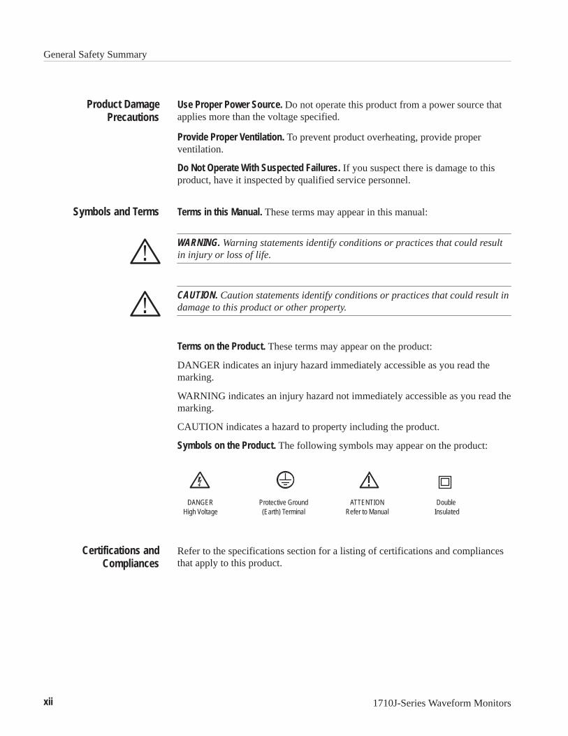
Use Proper Power Source. Do not operate this product from a power source thatapplies more than the voltage specified.
Provide Proper Ventilation. To prevent product overheating, provide properventilation.
Do Not Operate With Suspected Failures. If you suspect there is damage to thisproduct, have it inspected by qualified service personnel.
Terms in this Manual. These terms may appear in this manual:
WARNING. Warning statements identify conditions or practices that could resultin injury or loss of life.
CAUTION. Caution statements identify conditions or practices that could result indamage to this product or other property.
Terms on the Product. These terms may appear on the product:
DANGER indicates an injury hazard immediately accessible as you read themarking.
WARNING indicates an injury hazard not immediately accessible as you read themarking.
CAUTION indicates a hazard to property including the product.
Symbols on the Product. The following symbols may appear on the product:
Protective Ground(Earth) Terminal
ATTENTIONRefer to Manual
Double Insulated
DANGERHigh Voltage
Refer to the specifications section for a listing of certifications and compliancesthat apply to this product.
Product DamagePrecautions
Symbols and Terms
Certifications andCompliances
1710J-Series Waveform Monitors xiii
Service Safety Summary
Only qualified personnel should perform service procedures. Read this ServiceSafety Summary and the General Safety Summary before performing any serviceprocedures.
Do Not Service Alone. Do not perform internal service or adjustments of thisproduct unless another person capable of rendering first aid and resuscitation ispresent.
Disconnect Power. To avoid electric shock, disconnect the main power by meansof the power cord or, if provided, the power switch.
Use Caution When Servicing the CRT. To avoid electric shock or injury, useextreme caution when handling the CRT. Only qualified personnel familiar withCRT servicing procedures and precautions should remove or install the CRT.
CRTs retain hazardous voltages for long periods of time after power is turned off.Before attempting any servicing, discharge the CRT by shorting the anode tochassis ground. When discharging the CRT, connect the discharge path to groundand then the anode. Rough handling may cause the CRT to implode. Do not nickor scratch the glass or subject it to undue pressure when removing or installing it.When handling the CRT, wear safety goggles and heavy gloves for protection.
Use Care When Servicing With Power On. Dangerous voltages or currents mayexist in this product. Disconnect power, remove battery (if applicable), anddisconnect test leads before removing protective panels, soldering, or replacingcomponents.
To avoid electric shock, do not touch exposed connections.
X-Radiation. To avoid x-radiation exposure, do not modify or otherwise alter thehigh-voltage circuitry or the CRT enclosure. X-ray emissions generated withinthis product have been sufficiently shielded.

Service Safety Summary
xiv 1710J-Series Waveform Monitors

1710J-Series Waveform Monitors xv
Preface
This manual documents the Tektronix 1710J-Series Waveform Monitor, serialnumbers B040000 and above. Information that applies to all instruments in theseries uses 1710J-Series Waveform Monitor as the product name. Informationthat is specific to one member of the series refers to the instrument by itsnomenclature, for example, discussion of the NTSC version of the instrumentrefers to it as the 1710J Waveform Monitor.
The information in this manual is intended for instrument operators and servicetechnicians. Operators should be familiar with basic television terms andmeasurements. Qualified service technicians should be familiar with basictelevision terms and measurements and also have moderate experience withanalog and logic circuits.
The information in this manual is divided into two categories:
Operating instructions that are intended for those who use the instrument tomake the measurements for which it was designed.
Servicing instructions that are intended for those who maintain the instru-ment.
The information in the book is clearly divided into these two categories by astriped warning page.
The material in this manual is arranged in a logical order, which allows bothoperating and servicing personnel to retrieve information with equal ease. Themajor topics in this book are:
Getting Started as follows details how to place the 1710J Waveform Monitorin service and how to use the instrument. This section contains a descriptionof the instrument, typical configurations, a list of accessories, installationinstructions, and a functional checkout procedure.
Operating Basics describes the front-panel controls and the rear panelconnectors and provides instructions for making elementary television signalamplitude measurements.
Reference discusses how to use the graticules to make measurements andprovides more detailed information on how to use the instrument.
Specifications provide tables that list the instruments operating limits.
Theory of Operation provides overview and circuit specific discussions ofhow the instrument operates.

Preface
xvi 1710J-Series Waveform Monitors
Performance Verification provides a set if procedure for determining if theinstrument is performing within its stated performance requirements or not.
Adjustment Procedure provides the means to return the instrument tooperation within its stated requirements.
Maintenance provides the servicing instructions for 1710J-Series WaveformMonitor. These instructions include the service strategy, setting of internalplug jumpers to customize instrument operation, removal and replacementinstructions for the various assemblies that comprise this instrument,cleaning and inspection instructions, and troubleshooting information.
Replaceable Electrical Parts includes ordering information and part numbersfor all replaceable electrical parts.
Diagrams and Illustrations contain the block diagram, the circuit boardillustrations, the schematic diagrams, and the cross reference for locatingcircuit numbers on the circuit boards and the schematic diagrams.
Replaceable Mechanical Parts includes ordering information and partnumbers for all replaceable mechanical parts. This parts list is referenced toan exploded view mechanical drawing.
Index provides a topical listing of the information in this manual that isarranged alphabetically.

Preface
1710J-Series Waveform Monitors xvii
Contacting Tektronix
Productsupport
For questions about using Tektronix measurement products, calltoll free in North America:1-800-833-92006:00 a.m. – 5:00 p.m. Pacific time
Or contact us by e-mail:[email protected]
For product support outside of North America, contact yourlocal Tektronix distributor or sales office.
Servicesupport
Tektronix offers extended warranty and calibration programs asoptions on many products. Contact your local Tektronixdistributor or sales office.
For a listing of worldwide service centers, visit our web site.
For otherinformation
In North America:1-800-833-9200An operator can direct your call.
To write us
Web site
Tektronix, Inc.P.O. Box 500Beaverton, OR 97077-0001USA
www.Tektronix.com

Preface
xviii 1710J-Series Waveform Monitors

Getting Started


1710J-Series Waveform Monitors 1–1
Getting Started
This section of the manual has the product description, list of accessories,installation instructions, and a functional check of operation.
Product DescriptionThe Tektronix 1710J-Series is a specialized oscilloscope. It is designed tomonitor and measure baseband video signals. It offers a choice of three basicsweep rates: two field, two line, and 1 line, each of which can be magnified toprovide three additional sweep rates, 1 s (two line), 0.2 s (1one line), and X25(two field). The two-field sweep rate, both magnified and unmagnified displaysthe complete vertical interval.
The Channel A and B Composite Video Inputs and the External ReferenceSignal Input are high impedance bridging loop-throughs to protect the integrityof the signal paths. The input switching allows for the display of either Chan-nel A or Channel B Input or both inputs. Synchronization can be either internalor external.
The vertical signal processing provides slow DC restoration that clamps thedisplay while still showing any 50 or 60 Hz hum components. The input signalcan be unfiltered (Flat) or either Low Pass or Chrominance filtered. There is alsoa combination of Flat and Low Pass filtering available when a 2 Line or 2 Fieldsweep rate is employed; the display consists of one line or field low pass filteredwhile the second is unfiltered. Vertical amplitudes can be displayed in acalibrated gain mode, which corresponds directly with the graticule verticalscales, magnified five times.
An RGB or YRGB Parade display, for camera setup, is accommodated with ashortened sweep. The input of the camera signal and an enable are through therear-panel REMOTE connector. The choice of three-step (RGB) or four-step(YRGB) is made by changing the status of a control line through the REMOTEconnector.
The CRT is a mesh type, which has better geometry. In addition, it uses aninternal graticule to reduce parallax. Variable graticule scale illuminationprovides even lighting to improve measurement accuracy and the quality ofwaveform pictures. Option 74 provides a P4 (white) phosphor tube.

Getting Started
1–2 1710J-Series Waveform Monitors
Typical ConfigurationsIn addition to the typical master control monitoring applications, you can usethis waveform monitor in camera chains. It has a choice of RGB or YRGBparade display that can easily be selected by grounding or ungrounding one pinon the rear-panel REMOTE connector. The parade signal and the display enableare input through the rear-panel REMOTE connector.
A number of operating conditions can be altered by changing internal jumpers.Using these methods most of the 528A operational modes can be accommodated.
AccessoriesThe accessories listed here are in two categories. Standard accessories are theitems that you need to use the instrument as it is designed. Optional accessoriesare items that enhance the instruments usability or applications in a variety ofenvironments.
The following accessories are shipped with the 1710J-Series. Part numbers forthese accessories are located at the end of the Replaceable Mechanical Parts list.
1 1710J-Series Instruction Manual
1 Power Cord, with selected power plug option
1 Replacement Cartridge Fuse (correct rating for the power plug option)
3 Replacement Scale Illumination Bulbs
Standard Accessories
Getting Started
1710J-Series Waveform Monitors 1–3
There are a number of accessories that can be used with a 1710J-Series Wave-form Monitor. The following is a list of the most common accessory items forthis series of waveform monitors.
Cabinets are not supplied with the 1710J-Series instruments, order the appropri-ate cabinet or rack adapter from those listed below. The 1700F items are FieldUpgrade Kits that are installed by the customer; instructions are included in allField Upgrade Kits.
Cameras, C9 (Option 20)
Viewing Hood (016–0475–00)
Front Panel Cover (200–3897–01)
1700F00, Plain Cabinet (painted silver-grey)
1700F02, Portable Cabinet (painted silver-grey)
1700F05, Side-by-Side Rack Adapter
1700F06, Blank Half-Rack Width Panel
InstallationThis section provides the information necessary to install the 1710J-SeriesWaveform Monitor in its operating environment. Information on the settings ofthe internal jumpers appears in the Maintenance section of this manual.
The shipping carton and pads provide protection for the instrument duringtransit, they should be retained in case subsequent shipment becomes necessary.Repackaging instructions can be found in the Maintenance section of thismanual.
Electrical InstallationThe electrical installation for this instrument, because of its broad operatingrange power supply, consists of plugging it into any power mains that is withinits range.
This instrument is intended to operate from a single-phase power source withone current-carrying conductor at or near earth-ground (the neutral conductor).Only the Line conductor is fused for over-current protection. Systems that haveboth current-carrying conductors live with respect to ground (such as phase-to-phase in multiphase systems) are not recommended as power sources.
Optional Accessories
Packaging
Power Source

Getting Started
1–4 1710J-Series Waveform Monitors
All 1710J-Series Waveform Monitors operate over a frequency range of 48 to66 Hz, at any mains voltage between 90 VAC and 250 VAC. They do not requireany internal changes to select their operating voltage range.
REMOTE ConnectorThe rear-panel REMOTE connector is a 15-pin, D-type connector. It is the inputfor RGB Staircase and Enable signals. See Figure 1–1.
RGB ENBRGB
staircase
YRGB/RGB Gnd
12 11 10 915 14 13
5 4 3 2 18 7 6
Figure 1–1: REMOTE connector showing the RGB/YRGB functions
A TTL low level (ground) on pin 2 of the REMOTE connector enables theshortened RGB/YRGB sweep. A 10-volt square wave input to pin 1 providesapproximately nine divisions of sweep. This sweep can be either 1 line or 1 fielddepending on front-panel switch setting. The displayed signal is the front-panelselected CH A or CH B input.
A TTL low level (ground) on pin 10 of the REMOTE connector shortens thesweep for the three-step RGB display. A high level (open) on pin 10 lengthensthe sweep for the four-step YRGB display.
Connecting to the Program LineThe 1710J-Series Waveform Monitor uses high-impedance bridging loop-inputs.These inputs are compensated for 75 impedance systems but require termina-tion to avoid program line distortions. If the instrument is at the end of a line,you can use a standard 75 terminator on the open side of bridging loop-through input; however, be sure that the line is not double terminated, which willintroduce 6 dB of loss.
Mains Frequency andVoltage Ranges
RGB/YRGB ParadeDisplay
Getting Started
1710J-Series Waveform Monitors 1–5
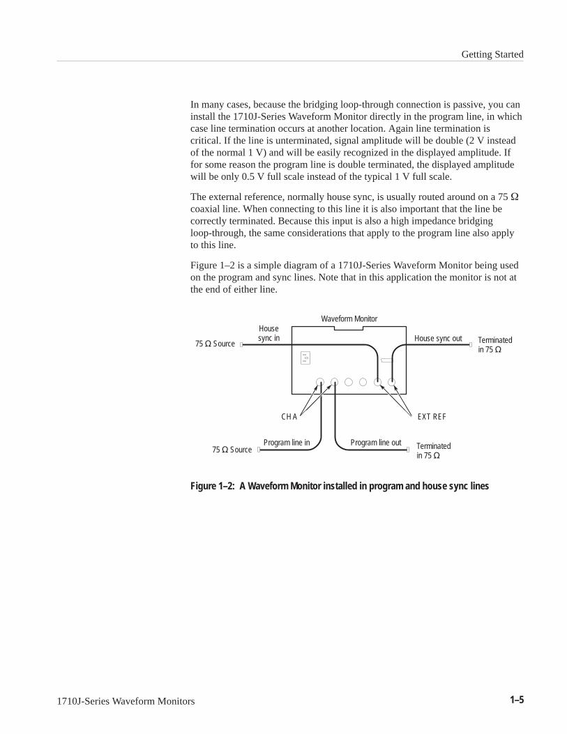
In many cases, because the bridging loop-through connection is passive, you caninstall the 1710J-Series Waveform Monitor directly in the program line, in whichcase line termination occurs at another location. Again line termination iscritical. If the line is unterminated, signal amplitude will be double (2 V insteadof the normal 1 V) and will be easily recognized in the displayed amplitude. Iffor some reason the program line is double terminated, the displayed amplitudewill be only 0.5 V full scale instead of the typical 1 V full scale.
The external reference, normally house sync, is usually routed around on a 75
coaxial line. When connecting to this line it is also important that the line becorrectly terminated. Because this input is also a high impedance bridgingloop-through, the same considerations that apply to the program line also applyto this line.
Figure 1–2 is a simple diagram of a 1710J-Series Waveform Monitor being usedon the program and sync lines. Note that in this application the monitor is not atthe end of either line.
Waveform Monitor
Terminatedin 75
Program line outProgram line in75 Source
CH A
Terminatedin 75
House sync outHousesync in
75 Source
EXT REF
Figure 1–2: A Waveform Monitor installed in program and house sync lines

Getting Started
1–6 1710J-Series Waveform Monitors
Mechanical InstallationThe mechanical installation for this instrument consists of mounting it in acabinet. The cabinet may be a portable cabinet with handle, feet, and flip stand,an unadorned cabinet that can be installed in a number of ways, or a side-by-siderack mounted cabinet assembly.
The EMI specifications for the 1710J-Series are only valid if the instrument ismounted in one of the three Tektronix cabinet options. To guarantee compliancewith specifications, the instrument must be operated in a 1700F00 or 1700F02cabinet, or a 1700F05 rackmount adaptor. The plain cabinet, 1700F00, is shownin Figure 1–3.
Rear
6.130
Bottom Side
12.725
8.2506.8750.688
1.060
16.180
5.105
0.156 Diameter (4)
Figure 1–3: Dimensions of the 1700F00 plain cabinet
The portable cabinet 1700F02 has a handle, four feet, a flip-up stand. The holesizes and spacing are different from those of the 1700F00. See Figure 1–4.
Cabinets

Getting Started
1710J-Series Waveform Monitors 1–7
3.310
Bottom Side
16.1809.435
0.141 Diameter (4)5.0001.625
Rear
8.2506.8750.688
5.105
Figure 1–4: 1700F02 portable cabinet
All of the 1700-Series metal cabinets, which are available from Tektronix asOptional Accessories, provide the proper electrical environment for theinstrument. They supply adequate shielding, minimize handling damage, andreduce dust accumulation within the instrument.
To install a cabinet on this instrument, slide the instrument into the cabinet andsecure it to the cabinet with two 6-32 Pozidrive screws through the holes in theupper corners of the rear panel. See Figure 1–5.
CAUTION. Without the mounting screws the instrument can slip out of thecabinet, if it is tipped forward. Do not attempt to carry a cabinetized instrumentwithout installing the mounting screws.
Cabinet Installation

Getting Started
1–8 1710J-Series Waveform Monitors
Cabinet mounting screws
Figure 1–5: Rear view showing the cabinet mounting screws
The 1700F05 is a side-by-side rack adapter that is made up of two cabinets. Itcan be used to mount the 1710J-Series and another half-rack width instrument ina standard 19-inch rack. See Figure 1–6.
Rear view
18.970
5.250
17.270
6.875
Mountingholes Controls front panel
to rack alignment.
Figure 1–6: The 1700F05 side-by-side rack adapter
Rack Adapter

Getting Started
1710J-Series Waveform Monitors 1–9
The rack adapter is adjustable, so the 1710J-Series Waveform Monitor can bemore closely aligned with other equipment in the rack. See Figure 1–6.
If only one section of the rack adapter is used, insert a 1700F06 Blank Panel inthe unused section. See Figure 1–7. The rack adapter and panel are availablethrough your local Tektronix field office or representative.
1700F05
1700F06
Figure 1–7: An instrument in a 1700F05 cabinet with a blank front panel
In addition to being able to fill the unused side of the side-by-side rack mountcabinet (1700F05) with a blank front panel, you can install an accessory drawer(1700F07) in the blank side of the cabinet. See Figure 1–8.

Getting Started
1–10 1710J-Series Waveform Monitors
1700F07
1700F05
Figure 1–8: A 1700F05 rack mounting cabinet with a 1700F07 utility drawer
For applications such as consoles the instrument can be mounted with frontmolding flush or protruding from the console. In both cases, allow approximate-ly 3 inches of rear clearance for bnc and power-cord connections. See Fig-ure 1–9.
To mount the 1710J-Series safely, attach it to a shelf strong enough to hold itsweight. Install the mounting screws through the four 0.156 inch diameter holesin the bottom of the 1700F00 cabinet.
Custom Installation

Getting Started
1710J-Series Waveform Monitors 1–11
Requires four 0.156 holes belowthe 1700F00 cabinet to secure the
instrument to the shelf.
For flush front panel: Cut hole thesame size as the monitor front moldingto allow the monitor front panel to align
with the custom panel surface.
For protruding front molding: Cut hole in panel the same size as theopening in the monitor cabinet to allowthe front panel molding to cover the hole.
Figure 1–9: Custom installation of an instrument cabinet

Getting Started
1–12 1710J-Series Waveform Monitors
Functional Checkout ProcedureThe following procedure is provided as an aid in obtaining a display on the1710J-Series Waveform Monitor (operator familiarization) and as a quick checkof basic instrument operation. Only instrument functions, not measurementquantities or specifications, are checked in this procedure. Therefore, a minimumamount of test equipment is required. All checks are made with the cabinet onand all internal jumpers in the factory-set position.
If performing the Functional Checkout Procedure reveals improper operation orinstrument malfunction, first check the operation of associated equipment. Ifassociated equipment is performing normally, refer the 1710J-Series WaveformMonitor to qualified service personnel for repair or adjustment.
When a complete check of the instrument performance to its specification isdesired, refer to the Performance Verification Procedure in this manual.
This procedure requires a source of composite video. The Tektronix 1410-SeriesTelevision Test Signal Generator (1410 for NTSC, 1411 for PAL) with Sync,Color Bar, and Linearity modules was used in preparing this procedure.
This procedure requires only one hook-up. Figure 1–10 shows the requiredconnections. Once the connections are made, continue on to step 1 of theprocedure.
1710J-Series Waveform Monitor
75 Terminator
To power mains
75 Terminator
Television Test Signal Generator
Color bar signal Linearity signal
Figure 1–10: Equipment connections for the functional checkout procedure
Procedure
Getting Started
1710J-Series Waveform Monitors 1–13
1. Initial Generator Setup
Video Signal Generator – Test Signals
Full Field Color Bars – 75% Ampl. 7.5% Setup – NTSC– 75% Ampl. 0% Setup – PAL
Modulated Staircase – Flat Field, 5 Step
2. Apply Power
Connect the instrument to a suitable AC power source and push the POWERbutton. A center dot should appear in the eye of the POWER switch to indicatethat it is on.
NOTE. Do not set any of the front-panel screwdriver controls until after theinstrument warms up (20 minutes minimum).
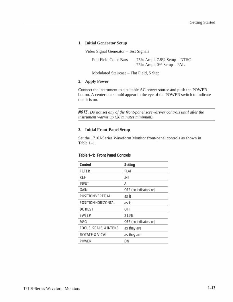
3. Initial Front-Panel Setup
Set the 1710J-Series Waveform Monitor front-panel controls as shown inTable 1–1.
Table 1–1: Front Panel Controls
Control Setting
FILTER FLAT
REF INT
INPUT A
GAIN OFF (no indicators on)
POSITION VERTICAL as is
POSITION HORIZONTAL as is
DC REST OFF
SWEEP 2 LINE
MAG OFF (no indicators on)
FOCUS, SCALE, & INTENS as they are
ROTATE & V CAL as they are
POWER ON

Getting Started
1–14 1710J-Series Waveform Monitors
4. Obtain Display
Adjust the INTENS and FOCUS controls for the desired brightness and a welldefined display. Adjust the VERTICAL Position control to place the displayblanking level on the graticule 0 IRE (NTSC) or 300 mV (PAL) line. Center thedisplay with the HORIZONTAL Position. See Figure 1–11.
0V
1.2
1.0
1.1
0.9
0.8
0.7
0.6
0.5
0.4
0.2
0.1
0PAL
–0.3
+0.7
Tek 2% & 4% K FACTOR
Figure 1–11: Two-line color bar display in flat filter mode
Adjust the SCALE illumination control for the desired graticule scale brightness.
5. Check the Rotation of the Display
Variations in the earth’s magnetic field may make adjustment of the ROTATEcontrol necessary at installation or whenever you move the instrument.
Check that the display blanking level is parallel to the horizontal axis. If not,adjust the ROTATE screwdriver adjustment until the sweep is parallel to thehorizontal axis.
6. Calibrate Display
The CAL mode on the REF switch enables the waveform monitor calibratorsignal.
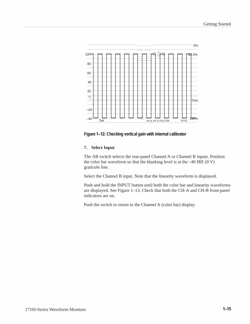
Press and hold the REF button until the CAL indicator LED is lit. Adjust theVERTICAL and HORIZONTAL position controls to obtain a display similar tothat shown in Figure 1–12.
If necessary, adjust the V CAL screwdriver control for 1 V amplitude (140 IRE).Switch REF to INT mode to restore the color bar display.
Getting Started
1710J-Series Waveform Monitors 1–15
100
80
60
40
20
–20
–40NTSC
7.5
12.5%
0%
75%
100%2% & 4% K FACTORTek
Figure 1–12: Checking vertical gain with internal calibrator
7. Select Input
The AB switch selects the rear-panel Channel A or Channel B inputs. Positionthe color bar waveform so that the blanking level is at the –40 IRE (0 V)graticule line.
Select the Channel B input. Note that the linearity waveform is displayed.
Push and hold the INPUT button until both the color bar and linearity waveformsare displayed. See Figure 1–13. Check that both the CH-A and CH-B front-panelindicators are on.
Push the switch to return to the Channel A (color bar) display.
Getting Started
1–16 1710J-Series Waveform Monitors
0V
1.2
1.0
1.1
0.9
0.8
0.7
0.6
0.5
0.4
0.2
0.1
0PAL
–0.3
+0.7
Tek 2% & 4% K FACTOR
Figure 1–13: Dual channel, 2-line display of color bar and linearity signals
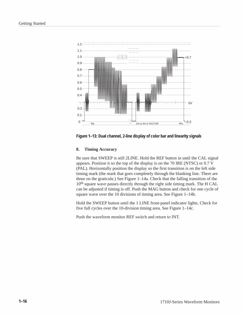
8. Timing Accuracy
Be sure that SWEEP is still 2LINE. Hold the REF button in until the CAL signalappears. Position it so the top of the display is on the 70 IRE (NTSC) or 0.7 V(PAL). Horizontally position the display so the first transition is on the left sidetiming mark (the mark that goes completely through the blanking line. There arethree on the graticule.) See Figure 1–14a. Check that the falling transition of the10th square wave passes directly through the right side timing mark. The H CALcan be adjusted if timing is off. Push the MAG button and check for one cycle ofsquare wave over the 10 divisions of timing area. See Figure 1–14b.
Hold the SWEEP button until the 1 LINE front-panel indicator lights. Check forfive full cycles over the 10-division timing area. See Figure 1–14c.
Push the waveform monitor REF switch and return to INT.

Getting Started
1710J-Series Waveform Monitors 1–17
60
40
20
–20
–40NTSC
7.5
75%
100%2% & 4% K FACTORTeka
60
40
20
–20
–40NTSC
7.5
75%
100%2% & 4% K FACTORTekb
60
40
20
–20
–40NTSC
7.5
75%
100%2% & 4% K FACTORTekc
Figure 1–14: Checking timing with the internal calibrator signal: a) 2-line display b)2-line display magnified c) 1-line display
9. Vertical Gain
The normal GAIN setting (with the GAIN switch off) is 1 V full scale with theX5 indicator off.
Push the GAIN button and check that the X5 indicator lights. Check for a largeincrease in gain. (It can be determined that this is a X5 gain increase by setting

Getting Started
1–18 1710J-Series Waveform Monitors
the signal base line on the graticule 0 IRE (NTSC) or 300 mV (PAL) andchecking that the maximum excursion of color burst is at approximately the100 IRE or 1 V graticule line.)
Push the GAIN button once and notice that the display amplitude returns to 1 VFull Scale.
10. Filter Selection
The FILTER button selects the frequency response characteristic for thedisplayed signal. Use the FLAT response normal applications. Figure 1–11shows the color bar signal with the FLAT response.
Press and hold the FILTER button to get the front-panel LPASS indicator tolight. This provides the low pass frequency response; the chrominance compo-nent of the signal has been removed. See Figure 1–15.
0V
1.2
1.0
1.1
0.9
0.8
0.7
0.6
0.5
0.4
0.2
0.1
0PAL
–0.3
+0.7
Tek 2% & 4% K FACTOR
Figure 1–15: Two-line color bar display with the low pass filter on
Press the FILTER button once more and look to see that the CHROMA indicatoris lit. The signal is now displayed as chrominance only; the luminance compo-nent is removed. See Figure 1–16.
Getting Started
1710J-Series Waveform Monitors 1–19
0V
1.2
1.0
1.1
0.9
0.8
0.7
0.6
0.5
0.4
0.2
0.1
0PAL
–0.3
+0.7
Tek 2% & 4% K FACTOR
Figure 1–16: Two-line display of color bar signal with chroma filter
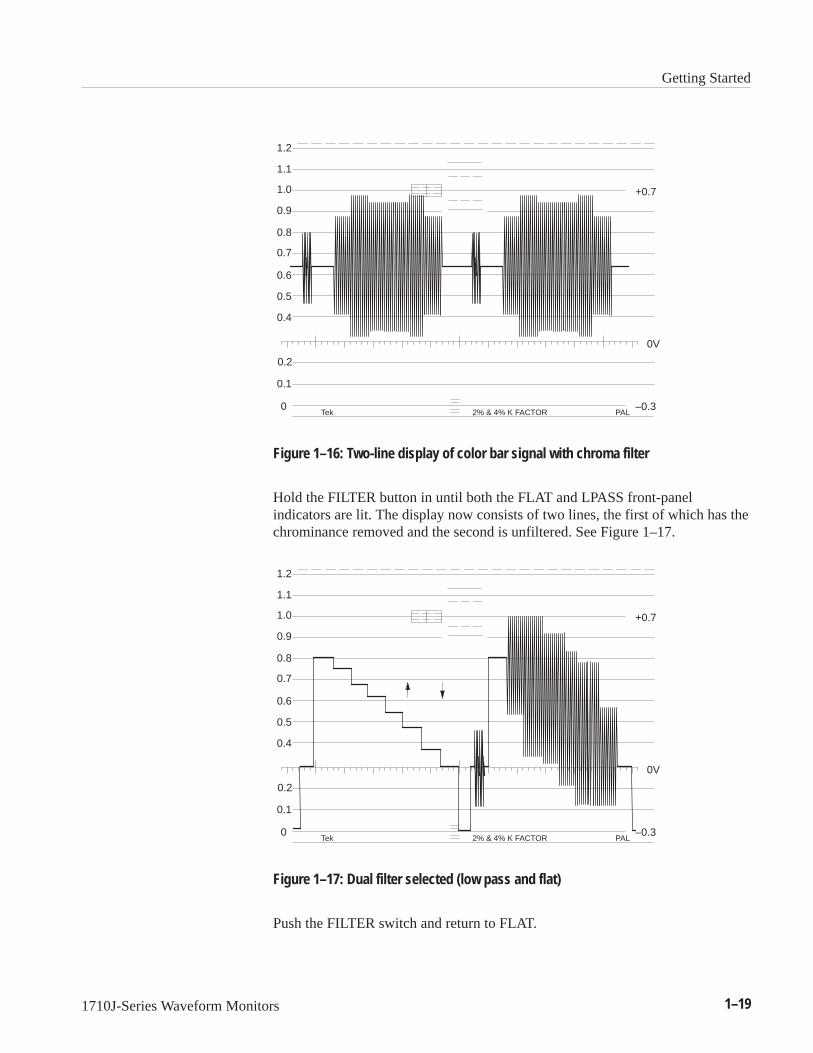
Hold the FILTER button in until both the FLAT and LPASS front-panelindicators are lit. The display now consists of two lines, the first of which has thechrominance removed and the second is unfiltered. See Figure 1–17.
0V
1.2
1.0
1.1
0.9
0.8
0.7
0.6
0.5
0.4
0.2
0.1
0PAL
–0.3
+0.7
Tek 2% & 4% K FACTOR
Figure 1–17: Dual filter selected (low pass and flat)
Push the FILTER switch and return to FLAT.

Getting Started
1–20 1710J-Series Waveform Monitors
11. Horizontal Magnifier
Select the 2 LINE SWEEP and center the horizontal sync on the screen. Press theMAG button and note the magnification of the horizontal sync details. PushSWEEP for 2FLD and MAG for X25 and note that the vertical interval isdisplayed. See Figure 1–18. Note that the MAG button works with any SWEEPselection. Push the MAG button to turn off the MAG.
0V
1.2
1.0
1.1
0.9
0.8
0.7
0.6
0.5
0.4
0.2
0.1
0PAL
–0.3
+0.7
Tek 2% & 4% K FACTOR
Figure 1–18: Display of vertical interval with magnified 2-field sweep

Operating Basics


1710J-Series Waveform Monitors 2–1
Operating Basics
This section of the manual provides information about the front-panel controlsand rear-panel connectors.
Front-Panel Controls and IndicatorsThe front-panel controls and indicators consist of momentary contact push-but-ton switches, variable controls, and backlit switch selections. See Figure 2–1 forcontrol and indicator locations.
14
109
5
1 2 3
8
13
4
76
11
12
Figure 2–1: 1710J-Series front panel controls

Operating Basics
2–2 1710J-Series Waveform Monitors
There are four push-button switches that have functions that are accessed byholding the switch down for approximately one second. These functions areidentified by a blue box surrounding the front-panel label. When exiting a heldmode the selection reverts to the top of the list at the touch of the push button,with the exception of the REF switch, which returns to its previous setting.
1. FILTER. The filter switch toggles through three positions, FLAT, LPASS,and CHROMA. In 2 LINE or 2 FLD SWEEP, a combination filteringroutine, consisting of Low Pass and Flat for alternate lines or fields, can beaccessed by holding the FILTER switch in. In the dual filter mode, the lowpass filtered line or field will always be on the left; lines are overlaid in1 LINE SWEEP. The dual filter cannot be accessed when the 1710J-Series isin AB switching. If AB switching is selected after the dual filter mode isselected, both lines or fields will be low pass filtered.
Filtering always returns to FLAT when coming out of the combinationfiltering routine.
2. REF. The reference switch toggles between internal and external reference.The calibrator is accessed by holding in the REF switch. Instrument status isretained in memory when CAL is selected and the original status restoredwhen you push the button again. All front-panel lights, except SWEEP andMAG, go out and GAIN goes to X1 when the calibrator is selected. The X5is not usable with the calibrator. (Note that MAG and SWEEP are switchablein the calibrator mode, but revert to their previous setting when the mode isexited.)
3. CH A - CH B. Toggles between the Channel A and Channel B input. Whenheld, the 1710J-Series goes into an AB (BOTH) alternate mode, with the Ainput on the left and the B input on the right in 2 Line or 2 Field (lines areoverlaid in 1 Line sweep). When in the AB switching mode the REF isforced to EXT, the FILTER is forced to LPASS, if it was in the LPASS-FLAT switching mode; if not the FILTER remains in the previous. Bothfunctions go back to their previous setting when the input is switched out ofAB. When leaving BOTH the input always returns to CH A.
4. The gain switch toggles between X5 and off. An LED indicator lightswhen X5 is selected.
5. POSITION. The vertical position knob controls the up and down movementof the display.
6. MAG. The magnifier switch toggles between on and off. It operates inconjunction with the SWEEP mode to provide usable sweep rates as follows:
2 LINE + MAG = 1 s/div
2 FLD + MAG = 1 full vertical interval

Operating Basics
1710J-Series Waveform Monitors 2–3
7. SWEEP. The sweep switch toggles between 2 LINE and 2 FLD Sweep.1 LINE Sweep is accessed by holding the SWEEP push button in untilrecognition occurs. The MAG is automatically turned off if SWEEP ischanged. Sweep rates are as follows:
2 LINE unmagnified = 10 s/div
1 LINE unmagnified = 5 s/div
1 LINE + MAG = 0.2 s/div
8. POSITION. The horizontal position knob controls the left and rightmovement of the display.
9. FOCUS. Focuses the CRT beam for optimum definition.
10. SCALE. Adjusts the level of graticule illumination.
11. INTENSITY. Adjusts the brightness of the display.
12. ON – OFF. Controls the output of the power supply. AC line potential ispresent in the primary section of the power supply circuit whenever mainspower is supplied to the instrument. A mechanical indicator in the center ofthe switch shows the status of the POWER switch.
WARNING. Mains power is still applied to the 1710J-Series power supply circuitboard, regardless of POWER switch state. To totally remove shock hazard it isnecessary to unplug the instrument and wait for the capacitors to discharge.
13. V CAL. The vertical calibration screwdriver adjustment sets the verticalamplifier gain. It is normally used with the calibrator.
14. ROTATE. The trace rotation screwdriver adjustment aligns the display withthe graticule.

Operating Basics
2–4 1710J-Series Waveform Monitors
Rear-panel ConnectorsSignal inputs, power and RGB are all located on the 1710J-Series WaveformMonitor rear panel. Because of the similarity of the half-rack monitor andhalf-rack vectorscope rear panels WAVEFORM MONITOR is printed on the1710J-Series rear panel. See Figure 2–2 for the locations of the rear-panelconnectors.
1 3
456
2
Figure 2–2: 1710J-Series rear-panel connectors
1. AC Power Plug. A standard AC plug receptacle for 120 or 240 VAC powermains. Plug is compatible with any of the power cord options available forthe 1710J-Series Waveform Monitor.
2. Fuse Holder. A holder for the instrument’s main fuse. See ReplaceableElectrical Parts List for the correct fuse value.
3. REMOTE. This 15-pin subminiature D-type connector is used for the RGBdisplay. It consists of the RGB input, RGB enable, and the display switch-ing, RGB/YRGB,
4. EXT REF. A bridging loop-through synchronization input (compensated for75 ). The signal on this input is selected as the synchronizing source by the

Operating Basics
1710J-Series Waveform Monitors 2–5
front-panel REF switch. The input signal may be composite sync, blackburst, or composite video.
5. CH-B. A bridging loop-through composite video input that is compensatedfor 75 . The signal on this input is selected for display by the front-panelINPUT switch.
6. CH-A. A bridging loop-through composite video input that is compensatedfor 75 . The signal on this input is selected for display by the front-panelINPUT switch.
Making a Signal Amplitude MeasurementThe 1710J-Series Waveform Monitor can make both time and amplitudemeasurements. The short procedure that follows allows you to locate theblanking level, measure the sync amplitude, and measure the peak white level.Timing measurements are more complex, they are discussed in the Referencesection of this manual.
1. Signal Input. Connect a 1 V color bar signal to one of the inputs of the1710J-Series Waveform Monitor, preferably Ch-A, and terminate theloop-through input with a 75 terminator. For the remainder of thisprocedure this input signal will be referred to as “the signal.” This signal canbe from a generator or off of a program line.
2. Obtain a Display. Turn on the 1710J-Series Waveform Monitor POWER,select CH A INPUT, FLAT FILTER, and INT REF. Set HORIZONTALSWEEP to 2 LINE and MAG off. Adjust the DISPLAY controls asnecessary for a usable display. Use the VERTICAL and HORIZONTALposition controls to align the display with the graticule.
3. Check Instrument Vertical Calibration. Push and hold the REF switchuntil the CAL indicator lights. Use the VERTICAL position control to alignthe calibrator waveform with the graticule. See Figure 2–3.

Operating Basics
2–6 1710J-Series Waveform Monitors
100
80
60
40
20
–20
–40NTSC
7.5
12.5%
0%
75%
100%2% & 4% K FACTORTek
Figure 2–3: Checking vertical gain with internal calibrator
Align the bottom of the waveform with the graticule line for sync tip. This is–40 IRE for 1710J and 0 mV for 1711J.
If necessary adjust the 1710J-Series Waveform Monitor V CAL to set thepeak white level to 1.0 V for 1711J or 100 IRE for 1710J. It may benecessary to reposition the display and again adjust the V CAL to match the1 V signal amplitude to a 1 V display.
4. Measure Sync Amplitude. Push the INPUT REF switch to return to INT.This should now display a two line display of the color bar signal. SeeFigure 2–4.

Operating Basics
1710J-Series Waveform Monitors 2–7
0V
1.2
1.0
1.1
0.9
0.8
0.7
0.6
0.5
0.4
0.2
0.1
0PAL
–0.3
+0.7
Tek 2% & 4% K FACTOR
Horizontal sync pulse
White level
Figure 2–4: Two-line color bar display in flat filter mode
Use the VERTICAL position to move the signal blanking level to thegraticule 0.3 V line for the 1711J or 0 IRE line for the 1710J.
Measure the amplitude of the horizontal sync pulse.
5. Measure White Level. The white level can vary with the signal source. Forexample, NTSC color bar signals may be either 75% white or 100% white;therefore, the white level may be at 75 IRE or 100 IRE depending on thesource. (In most cases the color bar is at 75% white.)
With the blanking level on the correct graticule line, measure the white level.See Figure 2–4.
6. Measure Setup Level. (NTSC only) This measurement is for 1710J only.Push and hold the HORIZONTAL SWEEP switch until the 1 LINE indicatorlights. This changes the display to a single line of color bar signal. SeeFigure 2–5.

Operating Basics
2–8 1710J-Series Waveform Monitors
100
80
60
40
20
–20
–40NTSC
7.5
12.5%
0%
75%
100%2% & 4% K FACTORTek
Setup level
Figure 2–5: One line display for setup measurement on 1710J
Use the VERTICAL position to set the blanking level of the signal to the)IRE graticule line. Measure the amplitude of the level following the lastchrominance packet of the color bar. It should be at the dotted line labeled7.5.

Reference


1710J-Series Waveform Monitors 3–1
Reference
This section discusses how to use the graticules to make measurements.Following the graticules there is more information on the measurements that canbe made with the 1710J-Series Waveform Monitor.
GraticulesThere are two graticule patterns available for the 1710J-Series WaveformMonitors. They are etched into the CRT face and edge illumination. Thegraticule used by the 1710J is a 525 line/60 Hz NTSC Composite scale. The1711J has the CCIR 625 line/50 Hz graticule for the PAL color standard.
Because the internal graticule is on the same plane as the CRT phosphor iteliminates viewing and photographic parallax errors. The graticule is illumi-nated, using a front-panel SCALE adjust control, so that the level of graticulebrightness can be adjusted to optimum for viewing or photographing needs.
The major differences between the NTSC and PAL graticules are in the verticalscales. In the paragraphs that follow each of the vertical graticule scales will bediscussed separately, while the horizontal scales are discussed together.
The NTSC graticule has two main vertical scales to facilitate typical measure-ments. See Figure 3–1. The left side scale is marked in IRE units and extendsfrom –50 to +120 IRE in 10 IRE increments. An IRE unit is equal to 7.14 milli-volts. Black level setup is shown as a dashed line at 7.5 IRE.
There are ±2 IRE and ±4 IRE markings at the center of the –40 IRE line (synctip) to assist in measuring sync amplitude. This scale is designed to be used withthe 2 line and 2 field sweep rates.
The scale on the right side of the graticule is for measuring depth of modulation.The scale extends from 0% at the 120 IRE line to 100% at sync tip (–40 IREline).
The boxed area slightly to the right of center at the 100 IRE level is scaled in 2%and 4% increments for precise tilt measurements. This structure is designed towork with an 18 s half-amplitude duration (HAD), 2T bar. Use the set of solidand short dashed lines, to the left of the bar tilt measurement structure, tomeasure pulse-to-bar ratio; the scale is weighted to include K-Factor ratings of2% and 4%.
NTSC Composite VideoGraticule Vertical Scales

Reference
3–2 1710J-Series Waveform Monitors
100
80
60
40
20
–20
–40NTSC
7.5
12.5%
0%
75%
100%2% & 4% K FACTORTek
Figure 3–1: NTSC graticule
Making Measurements. To use the NTSC vertical scale to make line timedistortion and pulse-to-bar ratio measurements, set the signal blanking level atthe graticule blanking line (0 IRE) and position the leading edge of the Compos-ite Test Signal bar to the ascending arrow (just right of graticule center). Checkto see if insertion gain is unity. Check to see that the negative-going bartransition passes through the descending arrow.
To measure the K-Factor line time distortion, measure the largest deviation of thebar top (tilt or rounding) within the structure. The structure is designed to ignorethe first and last 1 s of the bar where short-time distortions (ringing, overshoot,undershoot, etc.) occur. The solid outer box equals a 4% K-Factor, while thedashed line inner box equals a 2% K-Factor.
NOTE. For signals with a bar HAD that exceeds 18 s, simply measure the bartop in increments by positioning the bar to the left or right from the leading ortrailing edge. Note that when the leading or trailing edge is on the appropriatearrow, the first or last 1 s is automatically excluded from the measurement.
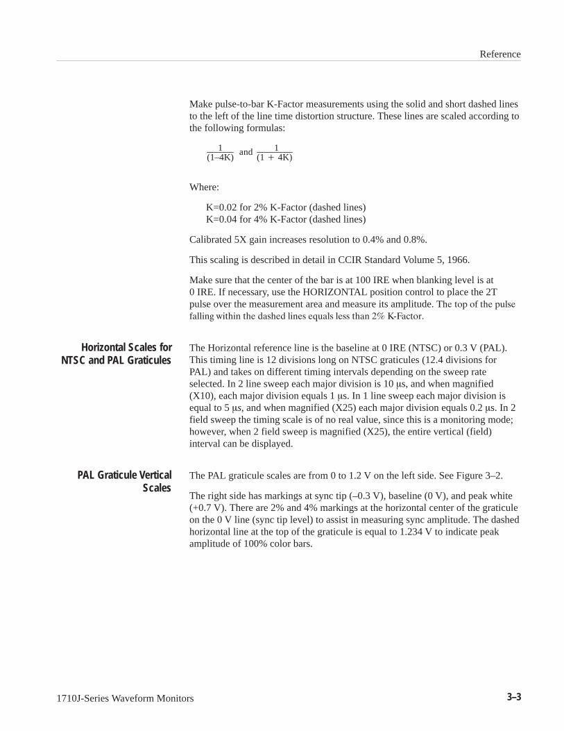
Reference
1710J-Series Waveform Monitors 3–3
Make pulse-to-bar K-Factor measurements using the solid and short dashed linesto the left of the line time distortion structure. These lines are scaled according tothe following formulas:
1(1–4K)
and 1(1 4K)
Where:
K=0.02 for 2% K-Factor (dashed lines)K=0.04 for 4% K-Factor (dashed lines)
Calibrated 5X gain increases resolution to 0.4% and 0.8%.
This scaling is described in detail in CCIR Standard Volume 5, 1966.
Make sure that the center of the bar is at 100 IRE when blanking level is at0 IRE. If necessary, use the HORIZONTAL position control to place the 2Tpulse over the measurement area and measure its amplitude.
The Horizontal reference line is the baseline at 0 IRE (NTSC) or 0.3 V (PAL).This timing line is 12 divisions long on NTSC graticules (12.4 divisions forPAL) and takes on different timing intervals depending on the sweep rateselected. In 2 line sweep each major division is 10 s, and when magnified(X10), each major division equals 1s. In 1 line sweep each major division isequal to 5 s, and when magnified (X25) each major division equals 0.2 s. In 2field sweep the timing scale is of no real value, since this is a monitoring mode;however, when 2 field sweep is magnified (X25), the entire vertical (field)interval can be displayed.
The PAL graticule scales are from 0 to 1.2 V on the left side. See Figure 3–2.
The right side has markings at sync tip (–0.3 V), baseline (0 V), and peak white(+0.7 V). There are 2% and 4% markings at the horizontal center of the graticuleon the 0 V line (sync tip level) to assist in measuring sync amplitude. The dashedhorizontal line at the top of the graticule is equal to 1.234 V to indicate peakamplitude of 100% color bars.
Horizontal Scales forNTSC and PAL Graticules
PAL Graticule VerticalScales

Reference
3–4 1710J-Series Waveform Monitors
0V
1.2
1.0
1.1
0.9
0.8
0.7
0.6
0.5
0.4
0.2
0.1
0PAL
–0.3
+0.7
Tek 2% & 4% K FACTOR
Figure 3–2: PAL graticule
The boxed area slightly to the left of center at the 1.0 V level is scaled for 2%and 4% K-Factor ratings for precise tilt measurements. This structure is designedto work with an 8 s, half-amplitude duration (HAD) bar. The short dashed linesto the right of the bar tilt measurement structure are used to measure pulse-to-barratio; they are weighted for 2% and 4% K-Factor ratings.
There are 2% and 4% markings near the horizontal center of the graticule on the0 V line (sync tip level) to assist in measuring sync amplitude. The dashedhorizontal line at the top of the graticule is equal to 1.234 V to indicate peakamplitude of 100% color bars. Between the 0.9 V and 1.1 V lines, there aremarkings at 20 mV intervals.
Making Measurements. To use the PAL vertical scale for measuring theK-Factor for line time distortion and pulse-to-bar ratio measurements, set thesignal blanking level at the graticule blanking line (0.3 V) and position theleading edge of the bar to the ascending arrow, just right of graticule center.Check to see if insertion gain is unity. Check to see that the negative-going bartransition passes through the descending arrow.
To measure the K-Factor for line time distortion, measure the largest deviation ofthe bar top (tilt or rounding) within the structure. The structure is designed toignore the first and last 1 s of the bar where short-time distortions (ringing,overshoot, undershoot, etc.) occur. The solid outer box equals a 4% K-Factor,while the dashed line inner box equals 2% line time K-Factor.

Reference
1710J-Series Waveform Monitors 3–5
NOTE. For signals with a bar half-amplitude duration (HAD) that exceeds 8 s,simply measure the bar top in increments by positioning the bar to the left orright from the leading or trailing edge. Note that when the leading and trailingedge is on the appropriate arrow, the first or last 1 s is automatically excludedfrom the measurement.
Pulse-to-bar K-Factor measurements are made using the solid and short dashedlines to the right of the line time distortion structure. These lines are scaled to thefollowing formulas:
1(1–4K)
and 1(1 4K)
Where:
K=0.02 for 2% K-Factor (dashed lines)K=0.04 for 4% K-Factor (dashed lines)
Calibrated 5X Gain increases resolution to 0.4% and 0.8%.
This scaling is described in detail in CCIR Standard Volume 5, 1966.
Make sure that the center of the bar is at 1.0 when blanking level is at 0.3. Ifnecessary, use the HORIZONTAL Position control to place the 2T pulse over themeasurement area and measure its amplitude. The top of the pulse falling withinthe dashed lines equals less than 2% K-Factor.
Analyzing a Video SignalAlthough television test equipment and test signals have evolved over the yearsto make video quality monitoring fast and easy, an experienced operator can keepthe signal under tight control using just a waveform monitor.
A television system works well over a wide range of conditions because thedestination equipment knows what to expect and makes a final presentation onthe viewing screen based on how the signal follows the rules. A part of the signalis very specific in controlling the operation of the receiving device and a part ofthe signal is free-form, where visual effects are created for the screen display.
Because the controlling elements are closely specified, an experienced operatorcan use this part of the signal to observe distortions in the transmission systemand predict the effect on the creative part of the signal.
Characteristics of the controlling parts of your video signal can help you read thequality of your system. The specific times set aside for this controlling signal areknown as the horizontal and vertical blanking intervals. Both intervals containvaluable clues to system performance.
The Test Signal in theVideo Signal

Reference
3–6 1710J-Series Waveform Monitors
The horizontal blanking interval is easily observed with a television waveformmonitor. The horizontal sync pulse has a specific amplitude and shape, and itstarts at a specific time in relation to the left and right edges of the picture. Theleft, falling edge of the horizontal sync pulse determines the lock and position ofthe picture on the screen. The color synchronizing burst keeps the receivingpicture monitor’s color decoder in step so that the intended color values may bereproduced. All of these blanking interval signals are standardized and manytransmission systems pass them through unmodified. Since they are knownsignal elements, they are useful as an indicator of signal path performance.
The shape of the horizontal sync pulse indicates mid-frequency distortions. Arounding or over-peaking of the corners can indicate short trailing smears orringing upon video signal transitions.
The amplitude (height) of the sync pulse (nominally 274 mV or 40 IRE units forNTSC or 300 mV for PAL) is an indicator of system gain. You want the samesync level (unity gain) through all sections of your signal path. Any notches inthe sync edges or sync tip could indicate signal reflections or ghosting caused byimproper cable termination or multiple over-the-air signal paths.
The size and shape of the color burst can tell you something about the color anddetail performance of your system. The color burst should be the same amplitudeas your sync pulse. The matching amplitude between the sync pulse and colorburst provides a two point frequency response check of your system, telling youthat the gain of your system is the same at a low and a high frequency.
If you have any doubt about how the horizontal blanking interval should look asthe composite signal progresses through your system, it does not have to beperfect, but it should look the same as it does at the source at every point downthe line.
To determine lower frequency distortions such as AC power hum or poor lowfrequency response you can look at your video signal at a slower rate. Set1710J-Series Waveform Monitor to display two fields (2 FLD). With dcrestoration off or in the slow position you can see any power line interferencemoving slowly right-to-left in the display. Poor low frequency response willcause abnormal brightness changes and horizontal banding in the picture and isan indication that maintenance may be required.

Reference
1710J-Series Waveform Monitors 3–7
The active video time is where the picture is carried. Here, too, you can tell quitea lot with just a waveform monitor. The video appears between the horizontalblanking intervals. Change or adjust the video signal and you will see a changein this signal. Select the the 1710J-Series Waveform Monitor LOWPASS filtermode to eliminate the chroma signal and show only the luminance, or brightnesssignal.
Creativity is allowed here, but the picture signal should use most of the areabetween the 7.5 IRE (maximum black for NTSC) dotted line (0.3 maximumblack for PAL) and the line at 100 IRE or 1.0 V(maximum white). If you do notuse all of this range, the picture will have a low-contrast, dark or washed-outlook. Most pictures will have some black, some white, and a range of values inbetween. If the average is more towards black, lighting may be uneven or theremay be too many reflections or highlights. Key elements may be too dark. If theaverage is toward white, the lighting is too flat. A few shadows may add richnessto the scene.
The Creative Part of theVideo Signal

Reference
3–8 1710J-Series Waveform Monitors

Specifications


1710J-Series Waveform Monitors 4–1
Specification
This section contains tables that list the specifications for the 1710J-SeriesWaveform Monitor All specifications are guaranteed unless noted “typical.”Specifications that are marked with the symbol are checked in the Perform-ance Verification section.
Values for the 1711J Waveform Monitor, when different from those called out forthe 1710J Waveform Monitor are shown in brackets[].
The performance limits in this specification are valid with these conditions:
The 1710J-Series Waveform Monitor must have been calibrated/adjusted atan ambient temperature between +20 C and +30 C.
The 1710J-Series Waveform Monitor must be in an environment withtemperature, altitude, humidity, and vibration within the operating limitsdescribed in these specifications.
The 1710J-Series Waveform Monitor must have had a warm-up period of atleast 20 minutes.
Table 4–1: Input/Output and Vertical Deflection
Name Description
Deflection Factor
1 V Full Scale 140 IRE [1.0 V] ±1% (1 V input signal displayed with FLAT FILTER)
X5 ±5% gain accuracy (1 V input signal displayed with FLAT FILTER)
Maximum Absolute Input Level ±5 V (DC + peak AC) Inputs over 200 IRE [1.428 V] may cause frequency responseerrors
DC Input Impedance Greater than 15 k, unterminated
Position Range 1 V signal positioned for peak white and sync tip levels at blanking level (0 IRE[0.3 V]) with the DC Restorer on at X1 or X5 gain
Frequency Response
Flat (X1 gain) 250 kHz to 6 MHz within 2% of response at 50 kHz (full screen height video inputsignal, 1 V Full Scale
Flat (X5 gain) 250 kHz to 6 MHz within 5% of response at 50 kHz
Low Pass Filter At least 30 dB attenuation at FSC (response at 15 kHz does not vary between FLATand LPASS by more than 1%)
Chroma Filter NTSC Nominal bandwidth 1 MHz; attenuation at 87.2 MHz, 20 dB or greater (response at3.58 MHz does not vary between FLAT and CHROMA by more than 1%)
Upper and lower –3 dB points are approximately ±350 kHz from 3.579545 MHz
15 to 35 C operating temperature

Specifications
4–2 1710J-Series Waveform Monitors
Table 4–1: Input/Output and Vertical Deflection (Cont.)
Name Description
Chroma Filter PAL Nominal bandwidth 1 MHz; attenuation at 8.9 MHz, 20 dB or greater. (response at4.43 MHz does not vary between FLAT and CHROMA by more than 1%)
Upper and lower –3 dB points are approximately ±350 kHz from 4.433619 MHz
15 to 35 C operating temperature
Transient Response, 1 V Full Scale or X5 Gain
Specifications apply for full screen height video input signal
Flat using 2T pulse and bar
Preshoot 1% or less
Pulse-to-bar ratioX1 GainX5 Gain
0.99:1 to 1.01:10.98:1 to 1.02:1
OvershootX1 GainX5 Gain
2% or less4% or less
RingingX1 GainX5 Gain
2% or less4% or less
Field Tilt 1% or less field rate square wave or vertical window
25 ms Bar Tilt 1% or less
Overscan Less than 2% variation in baseline of 100 IRE [700 mV] 12.5T [20T] modulated pulseas it is positioned over the middle 80% of the screen
Differential Gain Displayed differential gain is 1% or less with 10% to 90% APL changes
Chroma filter must be selected. Baseline at 50 IRE and displayed subcarrier adjustedto 100 IRE
Crosstalk between channels Typically greater than 50 dB of isolation between channels, measured at FSC betweenCH A, CH B and EXT REF
Loop-Through Isolation Typically greater than 50 dB of isolation between loop-through inputs, measured atFSC between CH A, CH B and EXT REF
Return Loss (75 ) Video Inputs (CH-A,CH-B)
At least 40 dB from 50 kHz to 6 MHz.
A and B channels, loop-through terminated in 75
Input in use or not in use, instrument power on or off, all deflection factor settings

Specifications
1710J-Series Waveform Monitors 4–3
Table 4–2: DC Restorer
Name Description
DC Restorer Clamp Time Backporch (J500 on/off)
Frequency Response at 60 Hz Slow — 20% or lessFast — 90% or greater
Attenuation of 60 Hz on input signal (J399 Fast/Slow)
Blanking Level Shift with 10% to 90% APLChange
APL changes from 50% to either 10% or 90% will cause blanking level shift of 1 IREunit [7.14 mV] or less
Blanking Level Shift Due to Presence orAbsence of Burst
1 IRE unit [7.14 mV] or less shift from no color burst to presence of color burst
Table 4–3: Calibrator
Name Description
Frequency 100 kHz, ±100 Hz, Synchronizes in 2H and 1H sweeps
Crystal controlled; timing accuracy is 10 s, ±0.01 s, Can be used as 10 s and1 s timing calibrator
Amplitude 140 IRE [1 V] within 1%
Position Top of waveform must be between 80 IRE (0.86 V) and 120 IRE [1.14 V] on graticulewhen backporch is positioned to 0 IRE [0.300 V] line, with DC RESTORER on
Table 4–4: Horizontal Deflection
Name Description
Sweep Sweep will occur in all Horizontal mode settings with or without synchronization
2 FLD Sweep Repetition Rate Equal to frame rate of applied video or external sync
2 FLD Sweep Magnification Approximately X25
1 LINE Sweep Repetition Rate Equal to line rate of applied video or external sync
2 LINE Sweep Repetition Rate Equal to half line rate of applied video or external sync
Sweep Length 2 LINE and 2 FLD sweep length is nominally 12.5 divisions
Timing Accuracy 1 s/division ±2%0.2 s/division ±3%
All timing and linearity specifications exclude the first and last major divisions of theunmagnified display
Linearity 1 s/division and 0.2 s/division
Within 2%
Differential Linearity 1 s/division and0.2 s/division
Within 2%
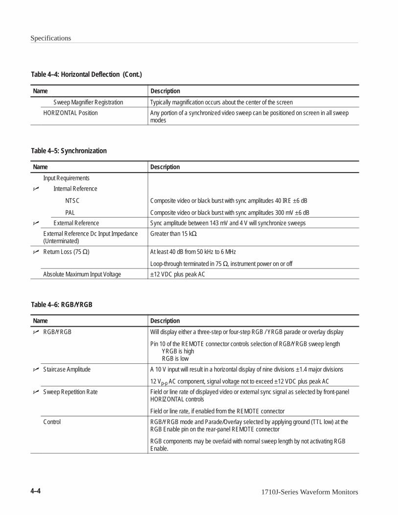
Specifications
4–4 1710J-Series Waveform Monitors
Table 4–4: Horizontal Deflection (Cont.)
Name Description
Sweep Magnifier Registration Typically magnification occurs about the center of the screen
HORIZONTAL Position Any portion of a synchronized video sweep can be positioned on screen in all sweepmodes
Table 4–5: Synchronization
Name Description
Input Requirements
Internal Reference
NTSC
PAL
Composite video or black burst with sync amplitudes 40 IRE ±6 dB
Composite video or black burst with sync amplitudes 300 mV ±6 dB
External Reference Sync amplitude between 143 mV and 4 V will synchronize sweeps
External Reference Dc Input Impedance(Unterminated)
Greater than 15 k
Return Loss (75 ) At least 40 dB from 50 kHz to 6 MHz
Loop-through terminated in 75 , instrument power on or off
Absolute Maximum Input Voltage ±12 VDC plus peak AC
Table 4–6: RGB/YRGB
Name Description
RGB/YRGB Will display either a three-step or four-step RGB / YRGB parade or overlay display
Pin 10 of the REMOTE connector controls selection of RGB/YRGB sweep lengthYRGB is highRGB is low
Staircase Amplitude A 10 V input will result in a horizontal display of nine divisions ±1.4 major divisions
12 Vp-p AC component, signal voltage not to exceed ±12 VDC plus peak AC
Sweep Repetition Rate Field or line rate of displayed video or external sync signal as selected by front-panelHORIZONTAL controls
Field or line rate, if enabled from the REMOTE connector
Control RGB/YRGB mode and Parade/Overlay selected by applying ground (TTL low) at theRGB Enable pin on the rear-panel REMOTE connector
RGB components may be overlaid with normal sweep length by not activating RGBEnable.

Specifications
1710J-Series Waveform Monitors 4–5
Table 4–6: RGB/YRGB (Cont.)
Name Description
Magnifier Typically X25 for 2 FLD, and X10 in 1 or 2 LINE
Sweep Length three-step: 3.4 — 4.1 divs.four-step: 2.5 — 3.1 divs.
Field or line rate sweeps
Table 4–7: CRT
Name Description
CRT Viewing Area Typically 80 × 100 mmHorizontal = 12.5 divisionVertical = 170 IRE units [1.19 V]
Accelerating Potential Typically 13.75 kV
Trace Rotation Range Greater than +1 degree from horizontal
Total adjustment range is typically 8 degrees
Graticule Internal, variable illumination
Table 4–8: Power Source
Name Description
Mains Voltage Range 90 - 250 V (Continuous range from 90 to 250 VAC)
Mains Frequency 50 or 60 Hz
Power Consumption 56 VA (35 watts)
Peak Inrush Current 9.1 A @ 90 VAC/50 Hz, 25.2 A @ 250VAC/50 Hz
Table 4–9: Physical Characteristics
Name Description
Dimensions Height: 5 1/4 in (133.4 mm)Width: 8 1/2 in (215.9 mm)Depth: 18 1/8 in (460.4 mm)
Weight Net: 8.5 lbs (3.8 kg)

Specifications
4–6 1710J-Series Waveform Monitors
Table 4–10: Environmental Characteristics
Name Description
Operating Temperature 0 to 50 C (+32 to 122 F)
Storage Temperature –40 to 75 C (-40 to 158 F).
Operating Altitude To 15,000 feet (4572 meters)
Storage Altitude To 50,000 feet (15,240 meters)
Vibration 5 minutes at 5 - 15 Hz with 0.060 in. displacement5 minutes at 15 - 25 Hz with 0.040 in. displacement5 minutes at 25 - 55 Hz with 0.020 in. displacementMilitary Specification: Mil-T-28800D, Paragraph 1.2.2, Class 3
Mechanical Shock Non-operating: 50 g 1/2 sine, 11 ms duration three shocks per surface (18 total)
Transportation Qualified under NSTA Test Procedure 1A, Category II (24 inch drop)
Humidity Will operate at 95% relative humidity for up to five daysDo not operate with visible moisture on the circuit boards
Table 4–11: Certifications and Compliances
EC Declaration of Conformity1 Meets intent of Directive 89/336/EEC for Electromagnetic Compatibility. Compliance wasdemonstrated to the following specifications as listed in the Official Journal of the EuropeanCommunities:
EN 50081-1 Emissions:EN 55022 Class B Radiated and Conducted Emissions
EN 50082-1 Immunity:IEC 801-2 Electrostatic Discharge ImmunityIEC 801-3 RF Electromagnetic Field ImmunityIEC 801-4 Electrical Fast Transient/Burst Immunity
Low Voltage Directive 73/23/EEC:EN 61010-1 Safety requirements for electrical equipment for measurement,
control, and laboratory useEN 61010-2-031:1994 Particular requirements for hand-held probe assemblies for
electrical measurement and test
EMI1 FCC 47 CFR Part 15, Sub-part B, Class A
Installation (Overvoltage) Category Terminals on this product may have different installation (overvoltage) category designations.The installation categories are:
CAT III Distribution-level mains (usually permanently connected). Equipment at this level is typically in a fixed industrial location.
CAT II Local-level mains (wall sockets). Equipment at this level includes appliances, portable tools, and similar products. Equipment is usually cord-connected.
CAT I Secondary (signal level) or battery operated circuits of electronic equipment.

Specifications
1710J-Series Waveform Monitors 4–7
Table 4–11: Certifications and Compliances (cont.)
Pollution Degree A measure of the contaminates that could occur in the environment around and within aproduct. Typically the internal environment inside a product is considered to be the same as theexternal. Products should be used only in the environment for which they are rated.
Pollution Degree 1 No pollution or only dry, nonconductive pollution occurs.Products in this category are generally encapsulated,hermetically sealed, or located in clean rooms.
Pollution Degree 2 Normally only dry, nonconductive pollution occurs.Occasionally a temporary conductivity that is caused bycondensation must be expected. This location is atypical office/home environment. Temporarycondensation occurs only when the product is out ofservice.
Pollution Degree 3 Conductive pollution, or dry, nonconductive pollution thatbecomes conductive due to condensation. These aresheltered locations where neither temperature norhumidity is controlled. The area is protected from directsunshine, rain, or direct wind.
Pollution Degree 4 Pollution that generates persistent conductivity throughconductive dust, rain, or snow. Typical outdoor locations.
Safety Standards
U.S. Nationally Recognized Testing Laboratory Listing
UL1244 Standard for electrical and electronic measuring and testequipment.
Canadian Certification CAN/CSA C22.2 No. 231 CSA safety requirements for electrical and electronic measuringand test equipment.
European Union Compliance Low Voltage Directive 73/23/EEC, amended by 93/69/EEC
EN 61010-1 Safety requirements for electrical equipment for measurement,control, and laboratory use.
Additional Compliance IEC61010-1 Safety requirements for electrical equipment for measurement, control, and laboratory use.
Safety Certification Compliance
Temperature, operating +5 to +40 C
Altitude (maximum operating) 2000 meters
Equipment Type Test and measuring
Safety Class Class 1 (as defined in IEC 1010-1, Annex H) – grounded product
Overvoltage Category Overvoltage Category II (as defined in IEC 1010-1, Annex J)
Pollution Degree Pollution Degree 2 (as defined in IEC 1010-1). Note: Rated for indoor use only.1 Conditions:
High-Quality shielded cables must be used to ensure compliance to the above listed standards.This product complies when installed into any of the following Tektronix instrument enclosures:
1700F00 Standard Cabinet1700F02 Portable Cabinet1700F05 Rack Adaptor

Specifications
4–8 1710J-Series Waveform Monitors

The following servicing instructions are for use only by qualified personnel. Toavoid injury, do not perform any servicing other than that stated in the operatinginstructions unless you are qualified to do so. Refer to all Safety Summaries beforeperforming any service.
WARNING


Theory of Operation


1710J-Series Waveform Monitors 5–1
Theory of Operation
The material in this section is subdivided into a general description, which issupported by the simplified and main block diagrams, and the detailed circuitdescriptions that use the schematic diagrams as illustrations. A thoroughunderstanding of the instrument starts with knowing how the major circuitblocks fit together, which is then followed by an understanding of the individualcircuit’s functions. These discussions of the 1710J-Series Waveform Monitorbegin with a brief, fundamental overview, then proceed on to the block diagram,and then go on to the individual circuit descriptions.
OverviewThe 1710J-Series Waveform Monitor is a specialized oscilloscope. It is designedto monitor and measure television baseband signals. See Figure 5–1. Signalsinput through either of the rear-panel 75 bridging loop-through inputs aresynchronously displayed on a CRT.
Vertical
Inputs:CH ACH B
EXT REF
Front panelcontrols
Microcontroller
HorizontalRemoteinterface
Sync
CRT
Switching
RGB Enable,RGB Input, RGB/YRGB
Switching
Figure 5–1: Simplified representation of a 1710J-Series Waveform Monitor
Front-panel mode switching is accomplished by a series of push-button switcheswhose status is being constantly polled by a microprocessor. In turn, themicroprocessor controls switching functions and circuit gains so that theinstrument can perform as a monitor or be used to make specific measurements.

Theory of Operation
5–2 1710J-Series Waveform Monitors
The low voltage power supply is a high-efficiency switching type. the highvoltage power supply provides 13 kV acceleration potential.
Block DiagramThe Block Diagram for the 1710J-Series Waveform Monitor is located on afoldout in Diagrams/Circuit Board Illustration section of this manual. Thefollowing functional description uses the diagram as its illustration. The numberson the circuit blocks correspond to the schematic diagram where that circuitblock is detailed.
Color-encoded video signals are input through the bridging channel A andchannel B inputs. The input amplifiers are shunted by sample-and-hold-typeclamps, that are timed by a back porch sample from the back porch generator.Switching at the output of the amplifiers provides for display of either inputsignal or a combination of both in all sweep modes. In the combination mode,the channel A signal is displayed on the left of the CRT with the channel Bfollowing.
Front-panel switching can select a flat (unfiltered), a low pass, or a chromafiltered signal for display. Low pass filtering can be used with flat as part of thedual filter mode. In dual filter mode, the low pass filtered signal is displayed tothe left with the unfiltered (flat) signal following. When the calibrator signal isselected (from the front-panel switching), a 1 volt, 100 kHz signal is applied tothe input of the gain cell instead of input video. The calibrator signal is used toset up both vertical gain (volts full scale) and to check horizontal accuracy froma common, self-contained source.
Signal amplitude can be adjusted at the gain cell using the front-panel V GAINcontrol. The output signal from the gain cell drives another clamped amplifier.This second clamped amplifier has a loop-compensated sample-and-hold circuitto provide the fast clamping required for the fast dc restorer.
The vertical positioning voltage, along with the conditioned video signal, isinput to a switchable gain amplifier. Both amplifier gain and positioning rangecan be increased by a factor of 5 when X5 Gain is selected at the front panel. Thelimiter stage that follows prevents overdriving of the output amplifier.
The conditioned video signal and the Y component of the readout (from themicrocontroller) are input to the vertical output amplifier to match impedancesand normalize gain (approximately 40 V for 8 cm of vertical deflection) in orderto voltage drive the CRT vertical deflection plates.
Composite video from either internal (Channel A or B) or external reference hasall active video stripped away by the sync stripper to leave only sync to output asweep trigger.
Vertical
Horizontal

Theory of Operation
1710J-Series Waveform Monitors 5–3
The composite sync output of the sync stripper times a programmed logic array(PLA) that controls the horizontal and vertical sync generators. The syncgenerator H and V trigger outputs synchronize the sweep generator. If calibratoris selected, the cal drive signal from the microprocessor provides the sweepgenerator triggering signal.
The ramp signal, output by the sweep generator, drives the mag amplifier, whichprovides three gain ranges: X1 (un-magnified sweep), X10 (1 s/div. in two linesweep), and X25 (to display the full vertical interval in two field sweep, whileproviding 0.2 s/div. sweep rate in 1 line sweep). The horizontal positioningoffset voltage is input to the mag amplifier to ensure sufficient range to positionany part of the display onto the graticule.
When the RGB Parade display is enabled, the sweep is shortened. The RGBstaircase produces three short ramps per sweep that are displayed in sequence.
The output of the mag amplifier drives the horizontal output amplifier, whichmatches impedances and normalizes gain (approximately 100 V for a 10 cmsweep length) to drive the CRT horizontal deflection plates.
The Z-Axis control uses the blanking signal (unblanking) and the intensityvoltage to unblank the CRT during sweep time. When the sweep is magnified itsoff-screen portion is blanked to increase the on-off contrast ratio. The focusamplifier, which is controlled by the front-panel FOCUS control, provides avoltage to the CRT focus ring.
The CRT is of the Post Acceleration type, which requires a relatively highpotential difference between the cathode and post anode. The boost in secondanode voltage is provided by an encapsulated 4X multiplier. Trace rotationprovides compensation for the magnetic field surrounding the CRT.
Vertical Input, Diagram 1The video signal is input to the waveform monitor through amplifiers that can beclamped at back porch time. Once buffered by the input amplifiers, whose gain is–1, a channel switch selects the input to be filtered, drive the picture monitoroutput, serve as the internal sync source, and eventually be displayed on theCRT.
When an external reference (sync) source is used, the composite signal is inputthrough an ac-coupled amplifier, which also has a gain of –1. Selection of thesync source is accomplished by a switch that is made up of a common base pairand switching diodes. A clamped sync stripper is used to remove active videoinformation and regenerate a composite sync signal for use by time relatedmonitor circuits.
CRT, Unblanking, andHigh Voltage
Theory of Operation
5–4 1710J-Series Waveform Monitors
An accurate 100 kHz waveform from the microcontroller is amplified and itsamplitude set and controlled by the calibrator. Calibrator output is enabled andoutput through the vertical amplifier low pass filter. The calibrator enable is alsogenerated by the microprocessor.
The rear-panel Channel A and B inputs are high-impedance bridging loop-through inputs compensated for use in 75 systems. Each amplifier has its ownDC restorer that is turned on or off by repositioning a plug jumper (See Diagram5). Restorers are either both on or off.
Because the Channel A and Channel B input amplifiers are identical, circuitnumbers for the Channel A amplifier are used to simplify the remainder of thisdiscussion.
The input amplifiers are inverting feedback operational amplifiers with a gainof –1. The input resistor (Ri) is R196 and the feedback resistor (Rf) is R198. Aplug and jumper is provided to select input coupling. J197 is factory set to the1-2 position for ac coupling; it can however, be moved to the 2-3 position toprovide dc coupling by bypassing C197, the ac-coupling capacitor.
The DC restorer is a feedback sample-and-hold circuit. Sampling occurs whenU395A closes at back porch time to charge the hold cap (C398) When therestorer is selected U395D closes and the loop-compensated buffer amplifier(U495A) drives the input amplifier input summing junction through R197. Thetime constant of the restorer does not attenuate 50/60 Hz hum by more that 10%.
The input amplifier output signals drive the channel switch, U492. The signalselection is determined by the level of the CH-B signal at U492 (pin 10). WhenCH-B is low, channel B is selected; when it is high, channel A is selected. Thechannel switch output (pin 6) drives a current mirror with three current sources.
Q792 is the current source for the internal sync signal and Q791 is the currentsource for the remainder of the vertical. With a 1 V input signal there will be1.11 mA of signal current flowing through R392 (or R393) into the channelswitch. This signal current is available to drive the vertical through Q791.
Only 0.5 mA of signal current is available to drive the sync stripper throughQ792. Its emitter resistor, R694, is twice the resistance of R792 and R693, theemitter resistance for Q790.
The external sync signal from the rear-panel EXT REF loop-through is bufferedby an operational amplifier consisting of U795A and B. It has a gain of –1,which is determined by the combination of input resistor (Ri) R997 and feedbackresistor (Rf) R898. The operational amplifier output drives Q798, which is onecurrent source for the source switch (U795D).
Input Amplifiers
Channel Switch
External Sync Input andSource Switch

Theory of Operation
1710J-Series Waveform Monitors 5–5
The internal sync current source, for the other side of the common emitter SourceSwitch (U795D), is Q792. It provides signal current through pin 5 of U795Dwhich also forward biases CR696 when the switching signal (EXT) is high.CR698 keeps CR696 from conducting when external sync input is selected.
When external sync is selected, EXT (from Diagram 5) goes low, turning onU795 (pins 1, 2, & 3) so that signal current from Q798 (the external sync currentsource) forward biases CR697. The 0.5 mA of signal current from Q798(external) or Q792 (internal) drives into a common base stage, Q799, whichdevelops a 1 V video signal across R797.
The sync stripper removes the active video portions of the signal to generate thesync required for timing signals. The circuit detects the sync tip, stretches it(amplifies that portion of the signal), and generates a clean sync signal. Thecircuit responds well to pulses up to 1 MHz, then rolls off to eliminate any effectfrom subcarrier or high frequency noise at the sync level.
The sync stripper circuit consist of a two-stage amplifier and a clamp (or dcrestorer). Figure 5–2 shows a simplified schematic of the circuit. Both amplifierstages feed back sync level information to the clamp.
COMPSYNCOUT
U892BQ992&
U892C
Clamp
R992
Video In(Sourceswitch)
R993
Figure 5–2: Simplified block diagram of the sync stripper
The first stage of the amplifier inverts the video signal and clips it near the synctip. (The bandwidth of the sync stripper keeps the circuit from clamping to highfrequency components of the video signal.) This operational amplifier stage ismade up of Q992 and U892C. The gain setting resistors R993 (Ri) and R992 (Rf)let the amplifier provide high gain to the sync tip portion of the signal, but clipany signal components slightly above the sync level.
Sync Stripper

Theory of Operation
5–6 1710J-Series Waveform Monitors
During sync time, the clamp circuit maintains the output of the first amplifierstage at about +5 V, which is fed back to the clamp circuit, through CR990, tomaintain the proper level.
During non-sync times (active video), CR988 and CR989 are both on to shuntU892C and greatly reduce the gain. Shunting the active video limits thesaturation of U892C, which allows it to respond quickly to the next synctransition.
An inverting amplifier, U892B, is the second amplifier stage. It providesnegative-going sync and cleans up any remaining noise or active video on thesignal. Output of the second stage is also fed to the clamp.
The clamp circuit is formed around U892E and U892A. U892E and CR990 forma current switch. When the first stage output level is at sync tip, current flowsthrough U892E, which charges C887. At the same time U892B pulls down onCR887 to provide a discharge path for C887. The result of these opposingactions is to establish an equilibrium voltage on C887. At the end of sync timeU892C saturates and pulls down on CR990 to shut off U892E.
The three filters are driven from current source Q791 through one of the analogswitch sections of U786. Only one switch section will be closed at a time, asdictated by its enable, from the microprocessor (Diagram 5) going low.chrominance filters are clamped to ground when low pass filtering or flat isselected. In this condition Q777 and Q776 are turned on clamping the chromi-nance filter outputs to ground.
When the chrominance filter is turned on an additional bias current for the ac-coupled filters (3.58 and 4.43 MHz) is required. It is supplied by pulling theemitters of either CR671 or CR670 low with the microprocessor-generatedenable signal, which turns on Q775 to saturate Q774. When Q774 saturates itscollector goes to +11.8 V. Signal current from the enabled filter drives theemitter of a common base amplifier input to the gain cell (Diagram 2). At a0 VDC level 2 mA of bias current is added to 1 mA of signal current that drivesthe input of the Gain Cell.
When dual filter or dual input display is selected a blanking signal is required tomask any potential switching transit that might occur. Whenever CH B or FLATgoes active an RC circuit consisting of C94 (CH B) or C871 (FLAT) and R878and R885 generates a pulse through Q764. Q765 inverts the blanking pulse,which is input to the blanking circuitry on Diagram 4.
The calibrator is a common base amplifier, Q587, that is driven by a 100 kHzsquare wave from the microprocessor (Diagram 5). It is switched at the 100 kHzrate. The gain is set by adjusting R689, the Cal Amp. The emitter current drivesthe low pass filter (which is at least 30 dB down at 3.58 to 4.43 MHz) through ananalog switch, U585C, which is activated by the microprocessor-generated CAL.
Filter Selection
Calibrator

Theory of Operation
1710J-Series Waveform Monitors 5–7
Vertical Output, Diagram 2The filtered video signal drives the signal input of a gain cell whose gain iscontrolled by the front-panel V CAL. The gain normalized video signal drives anamplifier that can be clamped at back porch time with either a fast or slow timeconstant clamp, which is also selected by front-panel selection.
The switchable gain amplifier input is the dc level shifted (vertical position)output of the gain cell amplifier. Amplifier gain is switchable between X1 andX5 as selected by the front-panel X5 VERTICAL GAIN. Amplifier output drivesa bridge limiter that prevents the vertical output amplifier from being overdriven.
The vertical output amplifier is driven by the processed video signal or, in LineSelect, by an appropriate combination of video and the Y-axis portion of thereadout signal. The output amplifier has enough gain to drive the CRT deflectionplates, while providing the compensation for the deflection plate capacitance.
Q684 drives the gain cell. It is a low impedance (to terminate the filters)common base amplifier. The signal voltage off collector is approximately 0.5 V.
The gain cell (U578) is driven differentially; pin 1 is the signal input with a–3.0 VDC level plus the signal voltage. R675 determines the maximum gain ofthe gain cell. The amount of gain is controlled by varying the difference betweenthe bases of the two transistor pairs controlling the signal current flowing out ofpin 6 or pin 12. The front-panel V CAL control, R700, sets an input dc level onpin 10 of the gain cell.
The current flowing out of pin 6 drives the Gain Cell Amplifier, while thecurrent flowing out of pin 12 drives into a collector load, R480.
The gain cell amplifier is a clamped inverting operational amplifier driving boththe switchable gain amplifier and the second DC restorer. It consists of Q673,Q674, and Q669, with Q669, an emitter follower, operating as the output stage.Amplifier gain is approximately 4.
The DC restorer clamps the output level of the gain cell amplifier to the dc leveloccurring at back porch time. DC restorer drive is coupled through R474 into ananalog switch (U277B) that is activated by the BACKPORCH signal. U277Bcloses during back porch time to charge the hold cap, C484. The error amplifier(U488) drives a current summing point at the input of the gain cell amplifierthrough U585D. For slow restorer, R484 is in the loop compensation. However;for fast dc restorer, R484 is shorted to ground through U277C to speed up theloop time constant. The position of J99 controls the action of U277C.
Gain Cell
Gain Cell Amplifier
Second DC Restorer

Theory of Operation
5–8 1710J-Series Waveform Monitors
The switchable gain amplifier consists of Q476, Q477, and Q478, with Q469 asthe switching element. When the base of Q469 is pulled low through R472,amplifier gain is –1. Ri is R475 and Rf is the sum of R367 and R368. When itsbase is high, Q469 saturates and grounds the collector end of R470 to put anattenuator in the feedback path and increase gain by a factor of five. The output,at the collector of Q476, drives a bridge limiter circuit comprised of CR280 andCR380. See Figure 5–3 for a simplified diagram of the limiter.
The purpose of the limiter is to prevent the vertical output amplifier from beingover driven. The bridge limiter circuit, encompassing CR280 and CR380, isquiescently balanced (equal current through all arms) with no Vin. When there isa signal voltage (Vin) applied to the bridge (CR1-CR2), the output signal voltage(CR3-CR4) is approximately equal to the input. When Vin moves away from thequiescent state, the current in the bridge arms becomes unbalanced.
VIN
VOUT
1/2RL
1/2RL
1/3RL
+V
-V-V
+V
CR1
CR2
CR3
CR4
Figure 5–3: Simplified illustration of the bridge limiter circuit
When the bridge unbalances the current through the diodes changes, with morecurrent flowing into the load through either CR3 (positive excursion) or CR4(negative excursion), which turns the diode on harder. At the same time currentflowing through the complementary input diode CR1 (positive excursion) orCR2 (negative excursion) is reduced and the diode starts to turn it off. If thechange in Vin is large enough, the output diode takes all of the current (whichturns off the input diode) and disconnects the input from the output.
The bridge load, R378, R377, and R374, is also a voltage divider that sets theinput dc level for the vertical output amplifier at approximately –2 V.
Switchable Gain Amplifier
Theory of Operation
1710J-Series Waveform Monitors 5–9
The combination of Q382 and Q383 forms a shunt-feedback amplifier. Q382amplifies and inverts the collector current flowing in Q383 to provide most ofthe signal current through R485. Because the current across Q382 is nearlyconstant the input-signal voltage is applied directly across its emitter resistor,R485, with very little distortion. Negative feedback is employed to improvelinearity and reduce the thermal distortions introduced by Q383. In addition,negative feedback increases the input impedance. A series compensation networkconsisting of R384 and C384 provides improved bandwidth and stability.
The combination of Q385 and Q387 form a shunt-feedback amplifier, identicalto Q383 and Q382. The signal current for this amplifier is input through R485.Signal current through Q387 is equal in value and opposite in phase to thecurrent change in Q382. The Limit Center, R489, balances the bias currentflowing in Q382 and Q387. R387 and C387 form another series compensation toimprove bandwidth and stability. R486 and C389 provide high-frequencypeaking to improve the flat response; R385 and C385 improve low-frequencytransient response.
Q280 and Q289 are common-base stages that couple the complementary signalcurrents to the non-inductive CRT load resistors, R184 and R186. The resultingsignal voltages drive the CRT vertical deflection plates. R183 and R187 shuntthe load resistors to provide the proper load resistance for the high-bandwidthoutput signal. L180 and L190 are adjustable shunt-peaking coils to increase thevertical bandwidth and allow precise adjustment of flat response.
Timing, Diagram 3Composite sync from the sync separator (Diagram 1) is used to time thehorizontal and vertical sync generators. Outputs from these generators are usedto develop line and field rate signals that are used to display selected lines orfields of information. The clamp pulses used to time the vertical amplifier DCRestorers are generated by a back porch generator driven by the horizontal syncgenerator.
The input staircase for the RGB/YRGB parade display is input to an operationalamplifier through the rear-panel REMOTE connector. The compensatable (dclevel and transient response) RGB amplifier is enabled (RGB ENABLE) by aTTL low.
The timing state machine is U735. It, in conjunction with the microcontrolleroutputs control signals for input switching, calibrator drive, and the filterswitching on Diagram 1. In addition, it provides the clamp control pulses, sweeptriggers, and miscellaneous signals used by the microcontroller.
U735 is a quad 20-input logic array. It outputs a sync signal from pin 21 thattriggers the horizontal sync generator, which in turn outputs a regenerated
Vertical Output Amplifier
Timing State Machine

Theory of Operation
5–10 1710J-Series Waveform Monitors
horizontal sync. With the exception of composite sync, from the sync stripper onDiagram 1, all inputs the U735 are from the microcontroller on Diagram 5.Table 5–1 describes the signals output by the timing state machine.
Table 5–1: Timing State Machine Outputs
Signal Name Function
H TRIG Triggers signal that synchronizes the line sweep generator when compositesync signal is available. (To Diagram 4)
V TRIG Trigger signal that synchronizes the field sweep generator when compositesync is available. (To Diagram 4)
FLAT Closes a switch in the filter selection matrix when pulled low. (To Diagram 1)
LPASS Closes a switch in the filter selection matrix when pulled low. (To Diagram 1)
CH B Input switch control: CH A when high and CH B when low. (To Diagram 1)
SYNC SIG A sync signal that is phased to composite sync that is used as the syncgenerator synchronizing signal. (To Diagram 4)
Composite sync (SYNSIG) from U735 drives a non-retriggerable one shot,U844B, that triggers on the leading edges of horizontal sync pulses. The pulsewidth is wide enough to lock out half lines from the vertical interval. The outputof U844B are regenerate sync pulses, HSYNC and HSYNC. HSYNC is a clocksource for the PAL and drives the back porch one shot, U844A. The pulse widthis set to end at the start of the burst on the back porch of the composite syncsignal.
The back porch pulse for the DC restorer is generated by U844A and Q737.C843 and R837 set the position of the pulse. C848 and R849 determine the pulsewidth. The RC network, formed by R963, C964, C97, and R964 turns the outputof U844A into a pulse that drives Q99. The voltage follower formed by Q99 andR98 outputs the BACKPORCH pulse used by the clamp circuits to sample thecomposite signal during the backporch. During the vertical interval broad pulsesthere is no burst or backporch and therefore no pulse is desired. During thevertical broad pulses the SYNCSIG from U735 asynchronously clears U844A.
When the dual filter operating mode is selected (lowpass and flat) the filterinputs (Diagram 1) are switched, which generates a switching glitch during synctime. HSYNC, from U844B, and the GLITBLKEN are anded to form theGLITCH BLK signal for the Z-axis circuit to turn off the CRT beam during thisswitching transient. When the Q output of U844B goes low, during horizontalsync, U234D inverts it and inputs it to one input of U234B. If the dual filtermode is operating, GLITBLKEN (from the microcontroller on Diagram 5) ishigh and U234B outputs GLITCH BLK. R003 sets the pulse output amplitude.
Horizontal Sync Generator
Theory of Operation
1710J-Series Waveform Monitors 5–11
The composite sync signal also drives the vertical sync generator. The SYNCSIG is integrated by R947, C950, and U947A. During normal video lines andvertical serrated lines, the signal is mostly positive and charges the capacitor,C950, holding the output of U947A negative. During the vertical broad pulsesthe signal is mostly zero and the capacitor discharges making the output ofU947A go positive. The output then swings negative again after the broadpulses.
R850 and R751 offset the output of U947, which drives a comparator, U753B,through C853. U753B shapes the FIELD signal to the TTL level required todrive the microcontroller (Diagram 5) Interrupt 0 input. The voltage dividerformed by R850 and R751 also provides a 2.5 V source for the end of sweepcomparators in the sweep generator on Diagram 4.
U252 is a transistor array with two of the transistors connected as a differentialcurrent switch. The static output level (pin 8) is set by the front-panel INTENScontrol using Q243 (in the focus control) as a current source. The blanking signalis input to the transistor switching array through U252B (pin 9). When it goeshigh, the current output, collector of U252A (pin 8), is shut off and the Z-axisamplifier (Diagram 8) blanks the CRT.
Trace rotation compensates for changes in the magnetic field surrounding the1710J-Series Waveform Monitor. Q142 and Q143 are emitter followers toprovide trace rotation current to the CRT surrounding coil located inside the CRTshield. Amplitude and polarity are controlled by the front-panel ROTATEscrewdriver adjustment.
U263A is a triangle generator whose output is compared to the front-panelSCALE control output level, by U263B (a comparator). Whenever the output ofU263A is higher than the level from the front-panel SCALE control, Q158 isturned on and current is drawn through the bulbs (DS100, DS200, and DS300) toground. The duty cycle of Q158 is determined by the level set by the front-panelSCALE control.
The + and –15 V supplies generated by the main low voltage power supply arefurther regulated to meet the power requirements of the Main (A3) circuit board.U164 is the regulator; its reference level is set by R167, the –11.8 V adjust.U172 is the +11.8 V supply regulator and its reference level is set by R168, the+11.8 V adjust.
Vertical Sync Generator
Z-Axis Control
Trace Rotation
Graticule Illumination
Regulators
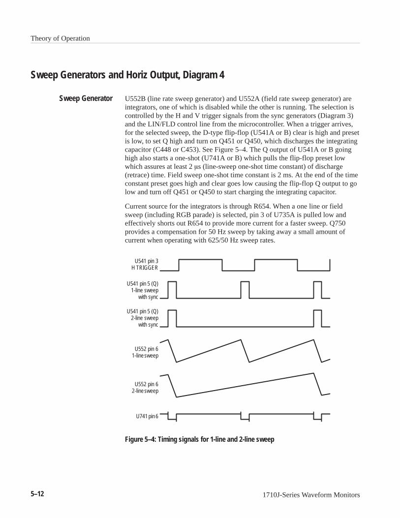
Theory of Operation
5–12 1710J-Series Waveform Monitors
Sweep Generators and Horiz Output, Diagram 4
U552B (line rate sweep generator) and U552A (field rate sweep generator) areintegrators, one of which is disabled while the other is running. The selection iscontrolled by the H and V trigger signals from the sync generators (Diagram 3)and the LIN/FLD control line from the microcontroller. When a trigger arrives,for the selected sweep, the D-type flip-flop (U541A or B) clear is high and presetis low, to set Q high and turn on Q451 or Q450, which discharges the integratingcapacitor (C448 or C453). See Figure 5–4. The Q output of U541A or B goinghigh also starts a one-shot (U741A or B) which pulls the flip-flop preset lowwhich assures at least 2 s (line-sweep one-shot time constant) of discharge(retrace) time. Field sweep one-shot time constant is 2 ms. At the end of the timeconstant preset goes high and clear goes low causing the flip-flop Q output to golow and turn off Q451 or Q450 to start charging the integrating capacitor.
Current source for the integrators is through R654. When a one line or fieldsweep (including RGB parade) is selected, pin 3 of U735A is pulled low andeffectively shorts out R654 to provide more current for a faster sweep. Q750provides a compensation for 50 Hz sweep by taking away a small amount ofcurrent when operating with 625/50 Hz sweep rates.
U541 pin 3H TRIGGER
U541 pin 5 (Q)1-line sweep
with sync
U541 pin 5 (Q)2-line sweep
with sync
U552 pin 61-line sweep
U552 pin 62-line sweep
U741 pin 6
Figure 5–4: Timing signals for 1-line and 2-line sweep
Sweep Generator

Theory of Operation
1710J-Series Waveform Monitors 5–13
If there is no H or V trigger, the output of the running sweep generator is selfretriggered. When the ramp amplitude reaches about 3/4 of its maximumamplitude U445B trips and sets the flip-flop preset high to turn on Q451 or Q450to start retrace. Just before retrace begins U445A also trips and pulls the flip-flopclear high to lock out the trigger signal and generate the HOLDOFF signal usedby the timing generator (Diagram 3) to phase up the horizontal timing of theinput or filter switching.
An operational amplifier consisting of U564C and D and Q566 positions andmagnifies the sweep signal. R557 and R558 are the central elements of thefeedback resistor network. The value of the network is altered by R552 (1 s cal)and R553 (0.2 s cal) when magnified sweep rates are selected. The junction ofinput resistance (R559) and the feedback resistance network (R557 and R558) isthe amplifier input summing junction.
Horizontal positioning voltage is input to an operational amplifier, U655B,which drives the mag amplifier summing point (along with the RGB staircasesignal, when RGB/YRGB operation is selected). The length of the sweep, inRGB mode, is set by jumper J456 to accommodate either three- or four-stepsweeps (for RGB and YRGB modes).
U465A and U465B are comparators used to sense when the output of themagnifier and position amplifier have driven the CRT beam to the edge of theCRT screen. When the beam is horizontally overdriven, the input to U234C ispulled low to generate the BLANK enabling level for the Z-axis amplifier(Diagram 3).
The horizontal output amplifier is composed of Q858, Q860, Q862, and Q864,with Q868 and Q865 serving as current source. R960 provides the differentialmode feedback; R958 and R959 provide the common mode feedback that biasesthe outputs to approximately 50 volts. The gain of the amplifier is determined bya voltage divider with two adjustments, R660 (sweep length adj.), and magnifiedsweep registration R661 (mag registration adj.).
Microcontroller, Diagram 5The microcontroller is the brain of the 1710J-Series Waveform Monitor. Itmonitors the front panel, and reacts to changes to any switch setting andgenerates appropriate control levels for circuits in the rest of the monitor.
The microcontroller interfaces the front-panel switching to the 1710J-SeriesWaveform Monitor control functions. The programmability and integration ofRAM, ROM, and counters provides flexible control over the complex switchingrequired for this waveform monitor. The microprocessor is equipped with
Magnifier Amplifier
Horizontal OutputAmplifier
Processor

Theory of Operation
5–14 1710J-Series Waveform Monitors
4 kbytes of one-time programmable EPROM, 128 kbytes of RAM, and two16-bit timer/counters. Its operating frequency, 12 MHz, is crystal controlled byY709. External instructions are imported and exported through a multi-functionserial port, and seven 8-bit bidrectional input/output ports. Port 0 and port 2 senddata to U407, the LED display controller. Port 1 monitors the front-panelpush-button switches and the 50/60 Hz input line. Port 4 is a static latch thatcontrols various instrument functions, such as magnifiers and sweep selections.Port 5 is a static and dynamic latch that extends the control functions of Port 4.
The FIELD and HSYNC are inputs from the timing (on Diagram 3). FRCLOCKis a freerun output clock used by the timing PAL on Diagram 3, when horizontalsync is not present.
The front-panel LED indicators are controlled by U407, which outputs 8 bits ofdata on bits SA – SD to provide the enables for the indicators. At the same timeone of the four bit lines, D1 – D4, turns on a transistor in a switching matrixconsisting of U305A – D. When one of the transistors is turned on it saturatesand provides the ground to close the circuit for one of the front-panel LEDs. Forexample, if bits SA and D1 are set high, U305A saturates and drives its collectorto ground, which turns on the FLAT indicator.
U331 divides the ALE (address latch enable) signal from the microprocessor(U522) by 20. When the calibrator is enabled U331 divides ALE down to outputthe 100 kHz CALDR (calibrator drive signal).
At power-up time, or after a power failure, the microcontroller presets the1710J-Series Waveform Monitor for a 2-line sweep, flat filtering, X1 gain andinternal sync.
There are a number of control lines, originating from the microcontroller.Table 5–2 lists these lines, the condition of the line and the expected results.
Table 5–2: Control Line Functions
Signal Line State Result
60/50 High Identifies NTSC or PAL standard. Needed for 2-field sweep
FIELD High Field rate output of the vertical sync generator. Used withHSYNC and 60/50 to identify fields and synchronize 2-fieldsweep, or synchronize dual filter or dual input switching
FRCLOCK High Has a frequency of approximately 3.91 kHz and is outputwhen HSYNC is absent
AD0 – AD7 ––– Address/data lines used to transfer data to U407
WR Low Latches data into U407
DCR EN Low Enables DC restorer
ALE ––– 2 MHz signal that is divided down to a 100 kHz pulse for thecalibrator drive

Theory of Operation
1710J-Series Waveform Monitors 5–15
Table 5–2: Control Line Functions (Cont.)
Signal Line ResultState
CAL Low Enables calibrator
LIN/FLD High 1 or 2 line display
Low 2 field display
TWO/ONE High 2 field or 2 line display
Low 1 line (no single field display possible)
X5 High Enables 5X vertical magnifier
EXT High Enables internal sync reference
Low Enables external sync reference
CH A High Enables CH-A input
CH B High Enables CH-B input
HMAG1 Low Enables magnifier in 2-line sweep
HMAG2 Low Enables magnifier in 1-line and 2-field sweep modes
3.58 Low Enables NTSC chrominance filter
4.43 Low Enables PAL chrominance filter
LPASS High Enables low pass filter
FLAT High Enables flat (no filter)
FIELDSWP High Enables field-rate sweep
ON DCR Low Enables DC restorer
GLITBLKEN Low Generates blanking pulse during H sync time in 2-line sweep
Under normal operation the base of Q856 is pulled down by CR955, whichcauses Q855 to saturate and ground the amplifier output. When exerted the RGBENABLE, from the REMOTE connector, is inverted to provide a discharge pathfor the emitter of CR955, which enables the RGB staircase amplifier.
The staircase signal from the REMOTE connector drives an operationalamplifier composed of Q856 and Q855, whose gain is approximately 0.5. Theamplifier is compensated, for optimum step definition (transient response), byC953. R856, the RGB offset adjustment, compensates for input dc levelvariation.
U331 divides down the microprocessor ALE output to generate cal drive. U331is enabled by the CAL from the I/O data latch, U532.
RGB Amplifier
Cal Drive

Theory of Operation
5–16 1710J-Series Waveform Monitors
The front-panel LEDs are driven in six common banks by U407. U305 providesa common current drain that is enabled by U407. Data registers in U407 arewritten into by the microprocessor over the eight-bit address bus and read out tofront-panel LEDs when WR goes low.
Front Panel, Diagram 6The front-panel indicators are driven from microcontroller light driver registerand LED drivers from Diagram 5. The front-panel switches are momentaryclosure (with some hold for additional function capabilities) that are monitoredby the microprocessor, which is also on the microcontroller (Diagram 5). Inaddition a series of front-panel controls provide variable dc operating levels as ameans of compensating for variable operating requirements and conditions.
The front-panel LED indicators are arranged in six columns returned to a currentsource by four returns, designated as rows, in order to provide the microproces-sor with a set of column/row matrix addresses. An LED indicator lights whenthere is a complete circuit from the light driver (Diagram 5) through the LEDand back to the light driver.
Switches complete a simple matrix that is read by Port 1 of the microprocessor.A completed circuit through the processor (switch closure) dictates an outputthrough the data I/O that changes one or more operating conditions. Some of theswitches are read in two different ways by the microprocessor. When touchedand released they cause the microprocessor to toggle to the next item on thatswitch’s menu. When held in, the microprocessor selects a specific operation.Hold for function switching options are outlined in blue on the front panel.
A set of variable controls consisting of the horizontal position, vertical position,vertical calibration, scale, and focus controls select a dc voltage level between+11.8 V and –11.8 V.
The INTENSity control operates in conjunction with the Z-axis control circuit onDiagram 3. DC levels for Intens 1, Intens 2, and Intens 3 depend on theoperating mode selected, which dictates the level on each of the leads.
LED Drive
Indicators and Switches
Controls

Theory of Operation
1710J-Series Waveform Monitors 5–17
Low Voltage Power Supply, Diagram 7The low voltage power supply converts the mains line voltage (90-250 VAC) tosupply the power requirements of the instrument. The voltages supplied by theLow Voltage Power Supply are +40 V, ±15 V, and +5 V.
The low voltage power supply is called a flyback switcher. When switcherMOSFET, Q9, is turned on, its drain voltage drops to approximately 0 V. Thecurrent through the 350 H primary winding of T3 begins ramping up. Thevoltages present at all secondaries is such that the rectifier diodes are reversebiased. Energy is being stored in the magnetic field of T3. When Q9 turns off,the drain voltage “flies back” in a positive direction. Current now flows in all ofthe secondary windings and supplies power.
The input line voltage is filtered by the rear-panel connector to reduce theelectrical noise conducted into or out of the instrument. R89 limits the initialcharging current through the rectifier diodes and C54.
CR21, CR22, CR23, and CR24 form a bridge rectifier. C54 filters the 110 to350 VDC rectifier output. L4 filters the switching noise produced by theswitcher. R102 reduces the circulating current in the parallel circuit consisting ofL4 and C44. DS4, R93, and R94 form a line voltage indicator. R91 and R92charge C42. C42 provides power to U5 until the primary housekeeping windingprovides power through CR17.
Line Rectifier and Filter
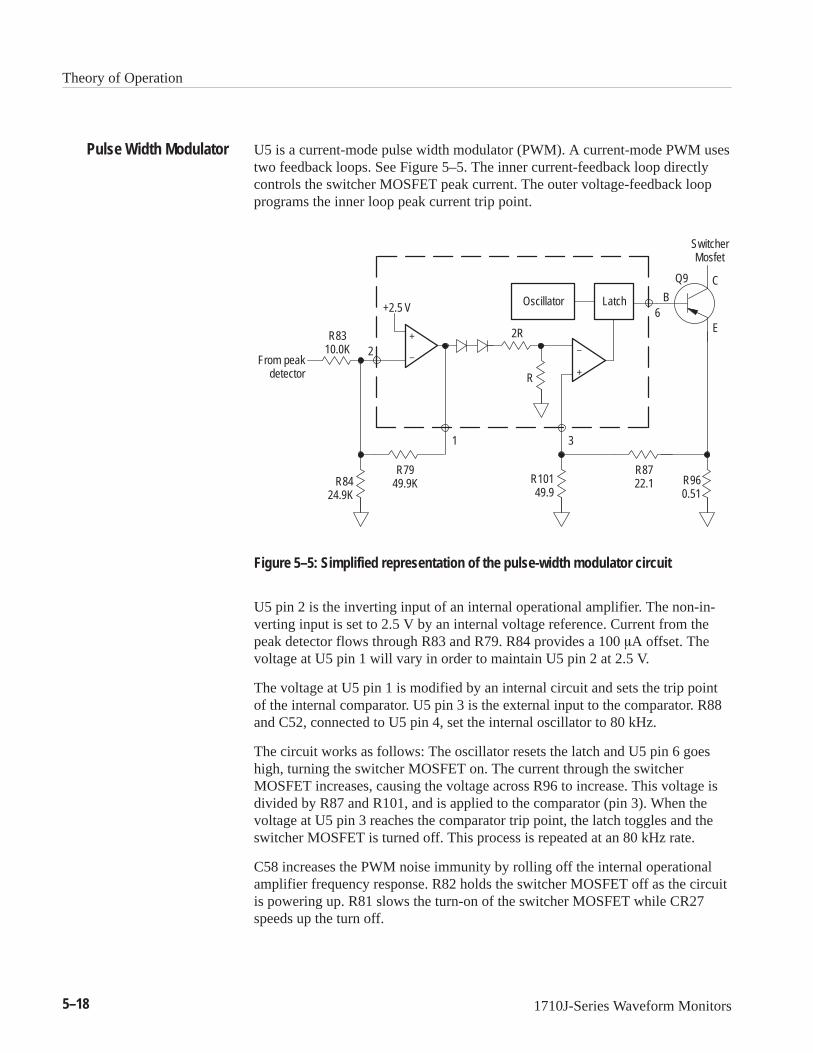
Theory of Operation
5–18 1710J-Series Waveform Monitors
U5 is a current-mode pulse width modulator (PWM). A current-mode PWM usestwo feedback loops. See Figure 5–5. The inner current-feedback loop directlycontrols the switcher MOSFET peak current. The outer voltage-feedback loopprograms the inner loop peak current trip point.
Oscillator Latch
From peakdetector
+2.5 V
E
BCQ9
SwitcherMosfet
R8310.0K
R7949.9K R101
49.9
R8722.1 R96
0.51
R
2R
6
31
2
R8424.9K
Figure 5–5: Simplified representation of the pulse-width modulator circuit
U5 pin 2 is the inverting input of an internal operational amplifier. The non-in-verting input is set to 2.5 V by an internal voltage reference. Current from thepeak detector flows through R83 and R79. R84 provides a 100 A offset. Thevoltage at U5 pin 1 will vary in order to maintain U5 pin 2 at 2.5 V.
The voltage at U5 pin 1 is modified by an internal circuit and sets the trip pointof the internal comparator. U5 pin 3 is the external input to the comparator. R88and C52, connected to U5 pin 4, set the internal oscillator to 80 kHz.
The circuit works as follows: The oscillator resets the latch and U5 pin 6 goeshigh, turning the switcher MOSFET on. The current through the switcherMOSFET increases, causing the voltage across R96 to increase. This voltage isdivided by R87 and R101, and is applied to the comparator (pin 3). When thevoltage at U5 pin 3 reaches the comparator trip point, the latch toggles and theswitcher MOSFET is turned off. This process is repeated at an 80 kHz rate.
C58 increases the PWM noise immunity by rolling off the internal operationalamplifier frequency response. R82 holds the switcher MOSFET off as the circuitis powering up. R81 slows the turn-on of the switcher MOSFET while CR27speeds up the turn off.
Pulse Width Modulator
Theory of Operation
1710J-Series Waveform Monitors 5–19
The three output windings supply four output voltages. Each output is rectifiedby a single diode and filtered by an LC pi filter.
The error amplifier regulates the +5 V output by feeding an error signal to thepulse width modulator. VR1 is a 2.5 V shunt regulator containing an operationalamplifier and a voltage reference. The +5 V is divided by R69 and R70 toprovide 2.5 V to VR1, with fine adjustment provided by R99. C40 and R71determine the gain and frequency response of VR1. VR4 controls overshoot ofthe +5 V at power up. R98 and CR26 provide a minimum operating current forVR1. R68 decouples C39 from VR1. Over-voltage protection for the +5V supplyis provided by a crowbar circuit formed by Q11, VR3, R13, and R14.
The 80 kHz sawtooth waveform at U3 pin 3 trips comparator U3. U3 pin 1 thenfeeds a trigger pulse to one shot U4. U4 pin 13 outputs a 300 ns pulse to the130 mA current source consisting of Q7 and Q8. When Q8 turns on, T2 pin 2 ispulled down until CR15 (error amplifier) is forward biased. The negative-goingpulse at T2 pin 2 is peak detected by CR16 and C46. The dc voltage present atthe anode of CR16 feeds the pulse width modulator and the output under-voltageshutdown circuit. CR29 resets T2 between pulses.
If the +5 V is below 4.9 V, the error amplifier will cause the peak detector outputto go below 2.9 V. The output of comparator U3B will pull low and shut downpulse width modulator U5. C47 and R96 delay the operation of U3B longenough for the power supply to power up. If the +5 V does not reach 4.9 Vwithin 50 ms of power up, U3B will shut down the switcher. The power supplywill then cycle on and off every couple of seconds.
High Voltage Power Supply, Diagram 8The high voltage power supply generates the heater, cathode, control grid, focusanode, and post accelerating potentials required to display the outputs of thevertical and horizontal output amplifiers.
The high voltage power supply is generated by a sine-wave oscillator and step-uptransformer. Q6 and T1 are the principal elements of an Armstrong oscillatorrunning at about 22 kHz. Error amplifier U2 regulates the +100 V output andkeeps the high voltage power supply constant under varying load conditions bycontrolling the base current to Q6. The +100 V output is regulated directly, whilethe high voltage power supply is indirectly regulated through a current feedbackcircuit.
Output Filters
Error Amplifier
Feedback TransformerDriver and Peak Detector
Output Under-VoltageShutdown
HV Osc and Error Amp

Theory of Operation
5–20 1710J-Series Waveform Monitors
R48, C16, R60, and R64 form the high voltage power supply current feedbackcircuit. As the current from the high voltage power supply is increased, thevoltage to the + side of the error amplifier (U2) increases, which increases thebase drive to Q6, the HV Osc. This current feedback compromises the regulationof the +100 V supply to keep the high voltage constant with varying intensities.
C66 and Q10 are a start delay circuit that holds the error amplifier output low,through CR30, until C66 is charged. Delaying the start of the high voltageoscillator allows the low voltage power supply to start, unencumbered by theload from the high voltage oscillator.
CR4 is the high voltage rectifier. Filter capacitors C3, C4, and C8 work withCR4 to provide –2530 V to the CRT cathode. U1 is a four-times multiplierproviding +11 kV to the CRT anode.
Q1 and Q2 form an operational amplifier that sets the voltage at the bottom ofthe focus divider. The front-panel FOCUS pot determines the voltage at thebottom of the focus divider. The center focus control, R11, is set for optimumbeam focus, as viewed on the CRT, with the front-panel FOCUS control set tomid range. Once the center focus adjustment has been set, adjusting thefront-panel FOCUS control changes the voltage at the bottom end of the dividerand, consequently, the voltage on the CRT focus anode.
The cathode of the CRT is at a –2750 V potential with the grid coupled to theZ-axis amplifier by the grid drive circuit. The grid is approximately 75 Vnegative with respect to the cathode. The 200 Vp-p sine wave present at thecathode of CR8 is input to the grid drive circuit where it is clipped for use asCRT control grid bias.
The sine wave from the cathode of CR8 is coupled through R47 to a clippingcircuit consisting of CR5 and CR6. Clipping level for the positive excursion ofthe sine wave is set by the CRT bias adjustment, R58. The negative clippinglevel is set by the front-panel INTENSITY control through the Z-axis amplifier.The clipped sine wave is coupled through C11 to a rectifier made up of CR1 andCR3. The rectified, clipped sine wave is the CRT control grid bias voltage. C9couples the blanking signal from the Z-Axis Amplifier to the CRT control grid.DS1 and DS2 limit the CRT grid to cathode voltage at instrument turn on or off.DS3 limits the CRT heater to cathode voltage.
Power Supply Outputs
Focus Amplifier
Grid Drive Circuit
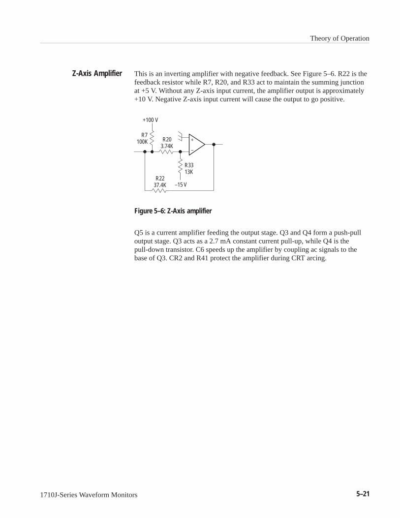
Theory of Operation
1710J-Series Waveform Monitors 5–21
This is an inverting amplifier with negative feedback. See Figure 5–6. R22 is thefeedback resistor while R7, R20, and R33 act to maintain the summing junctionat +5 V. Without any Z-axis input current, the amplifier output is approximately+10 V. Negative Z-axis input current will cause the output to go positive.
–15 VR22
37.4K
+100 V
R203.74K
R3313K
R7100K
Figure 5–6: Z-Axis amplifier
Q5 is a current amplifier feeding the output stage. Q3 and Q4 form a push-pulloutput stage. Q3 acts as a 2.7 mA constant current pull-up, while Q4 is thepull-down transistor. C6 speeds up the amplifier by coupling ac signals to thebase of Q3. CR2 and R41 protect the amplifier during CRT arcing.
Z-Axis Amplifier

Theory of Operation
5–22 1710J-Series Waveform Monitors

Performance Verification


1710J-Series Waveform Monitors 6–1
Performance Verification
This section contains procedures for verifying that the instrument performsaccording to the characteristics stated in the Specifications section of thismanual.
Limits, tolerances, and waveforms given in this section are guides for the checksand are not instrument specifications, except when listed in the the Specificationsection of this manual.
If failure is found, it is recommended that only those circuits that do not meetperformance criteria be adjusted. If adjustment fails to return the circuit to thespecified performance, refer to the Maintenance section of this manual.
Performance verification should be performed at regular intervals to ensure thatinstrument performance is within tolerance. The recommended interval forperformance verification is 2000 hours of operation or every 12 months,whichever is sooner.
Required Equipment ListTable 6–1 lists the test equipment required for this Performance Verification. Thecharacteristics specified are the minimum.
Table 6–1: Required Equipment
Test Equipment Characteristic Example
Test Oscilloscope Vertical amplifier bandwidth 30 MHz,sensitivity 1 mV, and accuracy of 0.25%
Horizontal deflection system 5 ms/div to1 s/div that can accept an external trigger.
Tektronix TAS465
Oscilloscope 10X Probe Tektronix P6137 probe
Oscilloscope 1X Probe Tektronix P6101 probe
Television Test Signal Generator (NTSC) Provide color bar signal, linearity staircasewith variable APL, pulse and bar (with 2Tpulse, 2T bar, and modulated pulse signals,
iel sq re ve si l m lti rst
Tektronix 1410 with Option AA and OptionAB (modified SPG2 and TSG7), TSG3,TSG5, and TSG6
Television Test Signal Generator (PAL) and field square wave signal), multiburstsignal, and black burst signalVariable color burst amplitude required
Tektronix 1411 with Option AA and OptionAB (modified SPG12 and TSG11), TSG13,TSG15, and TSG16.
Leveled Sine Wave Generator Frequency range, 250 kHz to 10 MHz Tegam SG503 Leveled Sine WaveGenerator
Function Generator Sine Wave frequencies 90 Hz to 2 kHz,amplitude 0.1 V to 10 Vp-p into 75 .
Tegam FG501A Function Generator

Performance Verification
6–2 1710J-Series Waveform Monitors
Table 6–1: Required Equipment (Cont.)
Test Equipment ExampleCharacteristic
Voltmeter Range, 0 to greater than 100 VDC;accuracy, ±0.1%
Frequency Counter Range, 100 kHz to 5 MHz; accuracy,±0.001%
Tegam DC503A Universal Counter/Timer
Video Amplitude Calibrator Signal, adjustable square wave 0.0 to999.9 mVp-p with a resolution of 0.1 mVand an accuracy of 0.05%; frequencyapproximately 270 Hz.
Tektronix 067–0916–00
Power Module For powering and housing Tegam SG503,DC503A, FG503, and Tektronix067–0916–00
Tegam TM506A
Variable Autotransformer Variable range of 90 –120 V (If 220 voltoperation must be checked, a conversiontransformer or appropriate 220 voltautotransformer is needed)
General Radio Metered Auto TransformerW10MT3W.
Spectrum Analyzer with Tracking Generator Bandwidth ≥10 MHz and sensitivity to50 dB
Tektronix 2712 Opt 04
Step Attenuator 75 constant impedance attenuatorvariable from 0 to 40 dB in 1 dB steps
Wavetek 75803 Step Attenuator
75 Terminators Three required, one should be a feed-through type
End-line, 75 terminator (Tektronix P/N011–0102–00) and a feed-through 75 terminator (Tektronix P/N 011–0103–02)
75 Coaxial Cable 42-inch RG59U, Three required Tektronix P/N 012–0159–00
10X, 75 Attenuator Tektronix P/N 011–0061–00
Alligator Clip to BNC Adapter Tektronix P/N 013–0076–00
Dual Input Coupler Matched bnc cable-T for making phasecomparisons between two inputs. Matchedlength of the two arms within ±0.1 inch
Tektronix P/N 067–0525–02
Precision 50 Coaxial Cable Used with the Sine Wave Generator Tektronix P/N 012–0482–00
50 -to-75 Minimum Loss Attenuator Tektronix P/N 011–0057–00
Parade Display Test Connector A 15-pin sub-miniature D-type connectormodified for RGB Parade input. SeeFigure 6–1
Tektronix P/N 131–0459–00

Performance Verification
1710J-Series Waveform Monitors 6–3
RGB ENBRGB
staircase
YRGB/RGB Gnd
12 11 10 915 14 13
5 4 3 2 18 7 6
Figure 6–1: RGB/YRGB parade display test connector
Verification ProcedureThis is a step-by-step procedure that begins with the powering up of theinstrument. There is a 20 minute warm-up time required after the 1710J-SeriesWaveform Monitor power is turned on.
This preliminary setup is the starting point for all parts of this procedure.
1. Set up the 1710J-Series Waveform Monitor front-panel controls as shown inTable 6–2.
Table 6–2: Preliminary Control Settings
Control Setting
POWER ON
INTENSITY Set to preference
FOCUS Set to preference
SCALE Set to preference
VERTICAL Position Set later
HORIZONTAL Position Set later
FILTER FLAT
REF INT
INPUT
GAIN (switch) off
MAG off
SWEEP 2 LINE
Preliminary Setup

Performance Verification
6–4 1710J-Series Waveform Monitors
2. Connect the AC power cord to the variable autotransformer. Turn power on1710J-Series Waveform Monitor and set the autotransformer for either 110or 220 Volts.
3. Use a 75 coaxial cable to connect a composite color bar signal from thetelevision test signal generator to the CH B input. Terminate the remainingside of the loop-through with a 75 end-line terminator.
The requirement is AC input range 90–132 V or 180–250 V.
1. Vary the autotransformer from 90–132 V or 180–250 V.
2. Check for stable operation over the voltage range.
3. Return the autotransformer to 110 or 220 Volts.
The frequency requirements are
Frequency 100 kHz ±100 Hz
Synchronizes 1 Line and 2 LINE Sweep (free runs in 2 FLD)
1. Connect a X10 probe from the frequency counter to the blue CRT lead on themain circuit board.
2. Display the CAL signal at the 2 LINE sweep rate.
3. Check that the frequency of the Calibrator is 99.9 to 100.1 kHz.
4. Check that the Calibrator is synchronized in both 1 LINE and 2 LINE sweep.
5. Check that sweep free runs in 2 FLD sweep.
The requirements are stable sweep synchronization are
Internally 40 IRE (300 mV) ±6 dB
Externally 143 mV to 4 V
1. Check that the 1710J-Series Waveform Monitor can be synchronized to theamplitudes shown in Table 6–3, using the television test signal generator.Check both 2 LINE and 2 FLD sweep for stable triggering.
Check Power SupplyOperation
Check CalibratorFrequency
Check Sync Separation

Performance Verification
1710J-Series Waveform Monitors 6–5
Table 6–3: Sync Amplitude
Reference Source Signal Sync Amplitude
Internal Composite Video 143 mV to 572 mV (NTSC)150 mV to 600 mV (PAL)
External Reference Composite Sync or Video 143 mV to 4 V (NTSC)150 mV to 4 V (PAL)
NOTE. !& !%!"!!
!# %!"!& ! !#" !
!!!"!$!&!!"! !!!"!
!!"! %!"
The operation requirements are
The correct sweep rate can be selected
Some part of the blanking interval is displayed when magnifying thecentered 2 LINE and 2 FLD sweeps
1. Display CH A input with nothing connected.
2. Check that a sweep occurs at each sweep rate (2 LINE, 2 FLD, and 1 LINE).
3. Select CH B input.
4. Check that the 1 LINE and 2 LINE sweep modes display one line and twolines of the color bar, respectively.
5. Check for a 2 FLD sweep display of the color bar signal.
6. Select and center the 2 FLD sweep and then push the MAG button.
7. Check that some portion of the vertical (field) blanking interval is displayed.
8. Select and center the 2 LINE sweep and then push the MAG button.
9. Check that some portion of the horizontal (line) blanking interval isdisplayed.
10. Check that both lines of the 2 LINE MAG sweep can be positioned onto thedisplay with the HORIZONTAL position control.
Check Sweep Operation

Performance Verification
6–6 1710J-Series Waveform Monitors
The requirements are shown in Table 6–4.
Table 6–4: Timing Accuracy
Sweep Range Timing Accuracy Timing Linearity Differential Linearity
1 Line ±2% ±2% ––––––
1 Line, Magnified ±3% ±2% ±2%
2 Line ±2% ±2% ––––––
2 Line, Magnified ±3% ±2% ±2%
1. Hold the 1710J-Series Waveform Monitor REF button in until the calibratorsignal is displayed.
2. Turn off the HORIZONTAL MAG and select 2 LINE sweep.
3. Use the HORIZONTAL position control to place the first falling calibratortransition on the 10 s graticule mark (the timing mark on the left side of thegraticule that goes completely through the blanking line). See Figure 6–2.
100
80
60
40
20
–20
–40NTSC
7.5
12.5%
0%
75%
100%2% & 4% K FACTORTek
Bracketed area represents the distancebetween 10 s and 110 s timing marks.
Figure 6–2: Ten full cycles of calibrator signal between timing marks
4. Check for ten full cycles of calibrator signal in the ten center major graticuledivisions, ±2% (one minor division).
Check Sweep Calibration

Performance Verification
1710J-Series Waveform Monitors 6–7
5. Check that no falling transition between the 10 s and the 110 s graticulemarks is more than 1% (0.5 minor division) from a major graticule mark.
6. Select 1 LINE sweep (push and hold).
7. Use the HORIZONTAL position control to place the first calibratortransition on the 5 s graticule mark (left side graticule timing mark).
8. Check for five full cycles of calibrator signal in the center ten major graticuledivisions, ±2% (one minor division).
9. Select 2 LINE sweep and turn on the HORIZONTAL MAG.
10. Check for one full cycle of calibrator signal in the center ten divisions of thegraticule, ±2% (one minor division).
11. Use a 75 coaxial cable to connect the television signal generator multi-burst output to the 1710J-Series Waveform Monitor CH A input.
12. Use a 75 coaxial cable to connect the other side of the loop-through to thedigital counter input.
13. Adjust the multiburst Frequency for a 5 MHz sine wave as measured on thedigital counter.
14. Select the 1710J-Series Waveform Monitor INT REF and 1 LINE sweep.Turn on the MAG
15. Set the multiburst generator to Composite.
16. Use the 1710J-Series Waveform Monitor HORIZONTAL position control todisplay all but the first and last 10% of the sweep.
17. Check for ten cycles over ten graticule divisions, ±1.5 minor divisions.
18. Switch the multiburst generator to Continuous and check that its frequency,as measured on the digital counter, remains set at 5 MHz. Return toComposite.

Performance Verification
6–8 1710J-Series Waveform Monitors
The requirements are shown in Table 6–5.
Table 6–5: RGB/YRGB Parade Display
Requirement Tolerance
Sweep Length
Three Step, RGB 3.4 to 4.1 divisions
Four Step, YRGB 2.5 to 3.1 divisions
Staircase input gain 10 V = 9 horizontal divisions±1.4 division
Attenuated sweep respondsto sweep rate and magnifica-tion controls
1. Use a 75 coaxial cable to connect the television test signal generator colorbar signal to the 1710J-Series Waveform Monitor CH A input. Terminate theremaining side of the loop-through with a 75 end-line terminator.
2. Display the color bar in 1 LINE sweep. Center the display. Note the positionof the plug on J456 on Assembly A3. The 2–3 position selects attenuationfor a three-step display (1–2 position selects attenuation for four-stepdisplay).
3. Install the parade display test connector on the 1710J-Series WaveformMonitor REMOTE connector. See Figure 6–1.
4. Check that the sweep has shortened to 3.4 to 4.1 divisions if P456 is set for athree-step display, or 2.5 to 3.1 divisions if the plug on J456 (1–2) is set for afour-step display.
5. Check that the shortened sweep is 1 LINE or 2 FLD, according to the sweepcontrols, and that the sweep can be magnified.
6. Check that the display can be moved to the sides of the screen with theHORIZONTAL position control. It may be necessary to adjust R856.
7. Position the display to the right side of the screen.
8. Use a 75 coaxial cable with the BNC connector-to-alligator clip adaptor toconnect a 0 to +10 V, 2 kHz square wave to pins 1 and 9 of the paradedisplay test connector.
9. Check that 7.6 to 10.4 divisions of deflection have been added by the squarewave.
Check RGB/YRGB ParadeDisplay

Performance Verification
1710J-Series Waveform Monitors 6–9
The requirements are
Gain within 1% for both CH A and CH B inputs
X5 gain within 5%
Less than 1 major division shift from baseline between unmagnified andmagnified signal
1. Use a 75 coaxial cable to connect the Video Amplitude Calibrator (VAC)output to the 1710J-Series Waveform Monitor CH A input.
2. Use a 75 coaxial cable to connect the television test signal generatorlinearity output to the CH B input. Do not terminate either loop-through. SeeFigure 6–3.
1710J-Series Waveform Monitor
Do not terminateTelevision Test Signal Generator
Linearity signal
Video AmplitudeCalibrator
Figure 6–3: Equipment hook-up for checking vertical gain
3. Set the VAC to 999.9 mV.
4. Move A3J500 to the (1–2) OFF position.
5. Adjust VCAL for exactly 140 IRE (1.00 V).
6. Set the VAC to 0.200 V and change the 1710J-Series Waveform MonitorGAIN to X5.
7. Check that the display is 133 to 147 IRE (0.950 V to 1.05 V).
8. Select CH B input.
9. Terminate the CH B loop-through with a 75 end-line terminator.
Check Vertical Gain

Performance Verification
6–10 1710J-Series Waveform Monitors
10. Use the VERTICAL position control to place the signal blanking level on thebaseline.
11. Select X5 GAIN.
12. Check for less than 1 major division of baseline shift when switchingbetween X1 (Gain off) and X5 GAIN.
13. Turn off X5 GAIN.
14. Remove the connections from the 1710J-Series Waveform Monitor CH Binput.
15. Change the 75 coaxial cable with the VAC signal to the CH B input. Donot terminate the loop-through.
16. Set the VAC for a 999.9 mV square wave.
17. Check that the vertical amplitude of the display is 138.6 to 141.4 IRE(0.990 V to 1.010 V).
18. Disconnect the VAC from the 1710J-Series Waveform Monitor.
The requirement is 1 V ±1%
1. Push the REF button and hold it in until the calibrator signal is displayed.
2. Check the 1710J-Series Waveform Monitor for a displayed amplitude of138.6 to 141.4 IRE PAL (0.990 V to 1.010 V).
The requirements are
Attenuation of 60 Hz input signal 20% or less
Blanking level shift with APL change, less than 1 IRE (7 mV)
Blanking level shift with presence or absence of burst, less than 1 IRE(7 mV)
1. Use a 75 coaxial cable to connect the television test signal generatormodulated five-step linearity signal (with AC Bounce on) to the 1710J-Se-ries Waveform Monitor CH B input. Terminate the remaining side of theloop-through input with a 75 Ω end-line terminator.
2. Use a 75 coaxial cable to connect the television test signal generator blackburst signal to the 1710J-Series Waveform Monitor EXT REF input.Terminate the remaining side of the loop-through input with a 75 Ω end-lineterminator.
3. Move A3J99 to the 2-3 position, Fast DC Restorer.
Check CalibratorAmplitude
Check DC RestorerOperation

Performance Verification
1710J-Series Waveform Monitors 6–11
4. Move A3J500 to the (2–3) ON position.
5. Display the signal with the 2 LINE sweep.
6. Select CH B input.
7. Position the signal blanking level to the graticule baseline (0 IRE or0.3 mV).
8. Switch television test signal generator linearity signal APL (Average PictureLevel) between 50% and 10% and 50% and 90%.
9. Check that the signal blanking level moves less that 1 IRE (NTSC) or 7 mV(PAL).
10. Use a 75 coaxial cable to connect the television test signal generatormultiburst signal to the CH A input. Terminate the remaining side of theloop-through input with a 75 end-line terminator.
11. Select CH A and EXT REF.
12. Switch multiburst generator Burst off and on.
13. Check that the blanking level changes less than 1 IRE (NTSC) or7 mV(PAL).
14. Remove the multiburst input from the CH A input.
15. Use a 75 coaxial cable to connect the function generator output through aX10 (75 ) Attenuator to the CH A input.
16. Move A3J500 to the 1–2 (off) position.
17. Set the function generator frequency to a 60 Hz (50 Hz PAL) sine wave. Setthe amplitude for a 100 IRE (700 mV PAL) 1710J-Series Waveform Monitordisplay.
18. Move A3J500 to the 2–3 (on) position.
19. Check that the display amplitude is 10 IRE (70 mV PAL) or less.
20. Move A3J99 to the 1–2 (slow) position.
21. Check that the display amplitude is 80 IRE (560 mV PAL) or greater.
22. Remove the signal cable and 75 terminator from the CHA input.
23. Move A3J500 to the (1–2) OFF position.
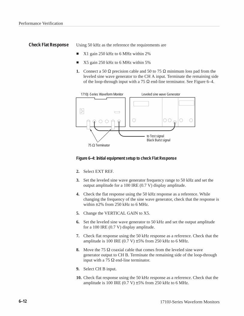
Performance Verification
6–12 1710J-Series Waveform Monitors
Using 50 kHz as the reference the requirements are
X1 gain 250 kHz to 6 MHz within 2%
X5 gain 250 kHz to 6 MHz within 5%
1. Connect a 50 Ω precision cable and 50 to 75 Ω minimum loss pad from theleveled sine wave generator to the CH A input. Terminate the remaining sideof the loop-through input with a 75 Ω end-line terminator. See Figure 6–4.
1710J-Series Waveform Monitor
75 Terminator
Leveled sine wave Generator
to Test signalBlack Burst signal
Figure 6–4: Initial equipment setup to check Flat Response
2. Select EXT REF.
3. Set the leveled sine wave generator frequency range to 50 kHz and set theoutput amplitude for a 100 IRE (0.7 V) display amplitude.
4. Check the flat response using the 50 kHz response as a reference. Whilechanging the frequency of the sine wave generator, check that the response iswithin ±2% from 250 kHz to 6 MHz.
5. Change the VERTICAL GAIN to X5.
6. Set the leveled sine wave generator to 50 kHz and set the output amplitudefor a 100 IRE (0.7 V) display amplitude.
7. Check flat response using the 50 kHz response as a reference. Check that theamplitude is 100 IRE (0.7 V) ±5% from 250 kHz to 6 MHz.
8. Move the 75 coaxial cable that comes from the leveled sine wavegenerator output to CH B. Terminate the remaining side of the loop-throughinput with a 75 end-line terminator.
9. Select CH B input.
10. Check flat response using the 50 kHz response as a reference. Check that theamplitude is 100 IRE (0.7 V) ±5% from 250 kHz to 6 MHz.
Check Flat Response

Performance Verification
1710J-Series Waveform Monitors 6–13
11. Turn off X5 VERTICAL GAIN.
12. Check the flat response using the 50 kHz response as a reference. Check thatthe response is within ±2% from 250 kHz to 6 MHz.
The requirements are shown in Table 6–6.
Table 6–6: Transient Response
Requirement Tolerance
2T Pulse and Bar
Preshoot 1% or less
Pulse-to-bar ratio 1:1 within 1%
Overshoot 2% or less
Ringing 2% or less
Tilt,field-rate square wave or25 s bar
1% or less
12.5T modulated pulse (20T forPAL) baseline overscan
Less than 2% over themiddle 80% of the display
1. Use a 75 coaxial cable to connect the television test signal generator pulseand bar signal to the CH B input. Terminate the remaining side of theloop-through input with a 75 end-line terminator.
2. Select INT REF.
3. Select the full amplitude 2T pulse and bar signal from the television testsignal generator. Display the signal with the 1 LINE sweep.
4. Check for less than 1% preshoot and less than 2% overshoot and ringing forthe pulse and bar transitions.
5. Check for a pulse-to-bar ratio within 1% of unity.
6. Check for less than 1% tilt across the bar.
7. Select the field square wave signal. Display the signal with the 2 FLDsweep.
8. Check for less than 1% tilt across the high APL portion of the display.
9. Set the 1710J-Series Waveform Monitor VERTICAL to X5 gain.
10. Select 2 LINE sweep and MAG ON.
11. Display the 12.5T modulated pulse for NTSC or 20T for PAL. Position thebaseline over the center 140 IRE (NTSC) or 1 V (PAL).
Check TransientResponse

Performance Verification
6–14 1710J-Series Waveform Monitors
12. Check that the baseline of the modulated pulse varies less than 2%.
The requirements are shown in Table 6–7.
Table 6–7: X5 Gain Transient Response
Requirement Tolerance
2T Pulse and Bar
Preshoot 1% or less
Pulse-to-bar ratio 1:1 within 2%
Overshoot 4% or less
Ringing 4% or less
1. Connect the black burst signal to the 1710J-Series Waveform Monitor EXTREF and terminate the remaining side of the loop-through input with a 75
terminator.
2. Turn MAG OFF. Select X5 VERTICAL GAIN and EXT REF.
3. Install the Step Attenuator and insert 14 dB of attenuation in the input signalpath.
4. Check for 1% or less preshoot and 4% or less overshoot and ringing for thepulse and bar transitions.
5. Check for a pulse-to-bar ratio within 2% of unity.
6. Disconnect signal from the CH B input.
The requirement is that response at 15 kHz does not vary between FLAT andLPASS by more than 1%.
1. Connect the modulated, five-step linearity signal to the CH B input.
2. Select the 100-IRE (100%) FLAT FIELD/ALT LINEARITY setting of thegenerator.
3. Select the LPASS FILTER and turn off X5 GAIN (X1).
4. Switch between LPASS and FLAT.
5. Check that the amplitude of the linearity signal, in LPASS, is within ±1% ofthe amplitude of the display in the FLAT mode.
Check X5 TransientResponse
Check Low Pass FilterResponse

Performance Verification
1710J-Series Waveform Monitors 6–15
The requirements are
Response at 3.58 MHz (4.43 MHz for PAL) does not vary between FLATand CHROMA by more than 1%
Attenuation at 7.2 MHz (8.9 MHz for PAL) is greater than 20 dB
1. Use a 75 coaxial cable to connect the leveled sine wave generator outputto the 1710J-Series Waveform Monitor CH B input. Terminate the remainingside of the loop-through input with a 75 end-line terminator.
2. Display the signal in FLAT with the 2 LINE sweep and EXT REF.
3. Set the leveled sine wave generator frequency to 3.58 MHz (NTSC) or4.43 MHz (PAL) and adjust the amplitude for 100 IRE (NTSC) or 700 mV(PAL).
4. Switch the FILTER to CHROMA
5. Check that the amplitude of the largest chrominance bar is 99 to 101% of theamplitude in step 3.
6. Select FLAT filter.
7. Set the leveled sine wave generator frequency to 50 kHz. Adjust theamplitude so that the display is 100 IRE (NTSC) or 700 mV (PAL).
8. Set the frequency of the leveled sine wave generator to 7.2 MHz (NTSC) or8.9 MHz (PAL).
9. Select CHROMA filter.
10. Check that less than 10% of the reference amplitude remains.
11. Move A3J500 to the (2–3) ON position.
The requirement is return loss of at least 40 dB from 50 kHz to 6 MHz (instru-ment on or off, any deflection factor setting).
NOTE. The Return Loss Check needs to be done only if repairs have been madeon the Input circuitry.
1. Connect a precision 50 cable from the spectrum analyzer RF Input to theRF Output on the RF bridge. See Figure 6–5.
2. Connect a precision 50 cable from the spectrum analyzer TG Output to theRF Input on the RF bridge.
Check Chrominance FilterResponse
Check Return Loss
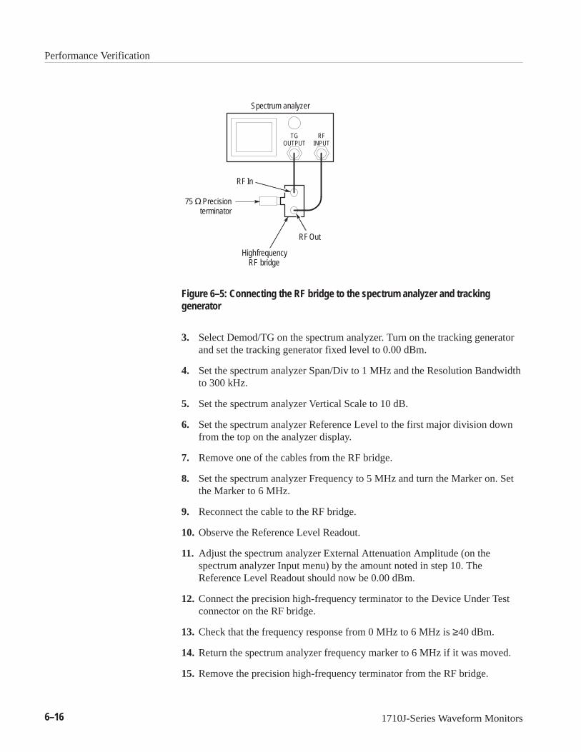
Performance Verification
6–16 1710J-Series Waveform Monitors
Spectrum analyzer
TGOUTPUT
RFINPUT
75 Precisionterminator
High frequencyRF bridge
RF Out
RF In
Figure 6–5: Connecting the RF bridge to the spectrum analyzer and trackinggenerator
3. Select Demod/TG on the spectrum analyzer. Turn on the tracking generatorand set the tracking generator fixed level to 0.00 dBm.
4. Set the spectrum analyzer Span/Div to 1 MHz and the Resolution Bandwidthto 300 kHz.
5. Set the spectrum analyzer Vertical Scale to 10 dB.
6. Set the spectrum analyzer Reference Level to the first major division downfrom the top on the analyzer display.
7. Remove one of the cables from the RF bridge.
8. Set the spectrum analyzer Frequency to 5 MHz and turn the Marker on. Setthe Marker to 6 MHz.
9. Reconnect the cable to the RF bridge.
10. Observe the Reference Level Readout.
11. Adjust the spectrum analyzer External Attenuation Amplitude (on thespectrum analyzer Input menu) by the amount noted in step 10. TheReference Level Readout should now be 0.00 dBm.
12. Connect the precision high-frequency terminator to the Device Under Testconnector on the RF bridge.
13. Check that the frequency response from 0 MHz to 6 MHz is ≥40 dBm.
14. Return the spectrum analyzer frequency marker to 6 MHz if it was moved.
15. Remove the precision high-frequency terminator from the RF bridge.

Performance Verification
1710J-Series Waveform Monitors 6–17
16. Connect the male-to-male bnc adapter to the Device Under Test connector onthe RF bridge.
17. Connect the Device Under Test connector on the RF bridge to the 1710J-Se-ries Waveform Monitor CH A input. Terminate the CH A loop-through withthe same precision high-frequency terminator used in step 15.
18. Select the 1710J-Series Waveform Monitor CH A input.
19. Check that the Reference Level Readout on the spectrum analyzer is≥40 dBm with the instrument power on and off.
20. Repeat steps 17 through 19 for CH B and EXT REF inputs.
21. Remove all cables and terminators from the 1710J-Series WaveformMonitor.

Performance Verification
6–18 1710J-Series Waveform Monitors

Adjustment Procedure


1710J-Series Waveform Monitors 7–1
Adjustment Procedure
If the instrument performance is not within tolerance for a particular characteris-tic, determine the cause, repair if necessary, and then use the appropriateadjustment procedure to return the instrument operation to performancespecification. After any adjustment, verify performance by repeating at least theapplicable part of the Performance Verification Procedure.
Allow the instrument to warm up for at least 20 minutes, in an ambienttemperature of 20 C to 30 C before making any adjustments. Waveformillustrations in the procedure are typical and may differ from one instrument toanother. These waveforms should not be construed as being representative ofspecific tolerances.
Static Discharge PrecautionsMany semiconductor components, especially MOS types, can be damaged bystatic discharge. Damage may not be catastrophic and, therefore, not immediatelyapparent. It usually appears as a degradation of the semiconductor characteristics.Devices that are particularly susceptible are MOS, CMOS, JFETs, and highimpedance operational amplifiers (FET input stages.) The damaged parts mayoperate within acceptable limits over a short period, but their reliability mayhave been severely impaired. Damage can be significantly reduced by observingthe following precautions during performance of the adjustment procedure.
Handle equipment containing static sensitive components or circuitassemblies at or on a static free work surface. Work stations should contain astatic free bench cover or work plane such as conductive polyethylenesheeting and a grounding wrist strap. The work plane should be connected toearth ground.
All test equipment and accessories should be connected to earth ground.
More information about handling static sensitive assemblies and components canbe found in the Maintenance section of this manual.
Required Test EquipmentTable 7–1 lists test equipment and fixtures recommended for the adjustmentprocedure. The characteristics specified ar the minimum required for the checks.Substitute equipment must meet or exceed these characteristics.
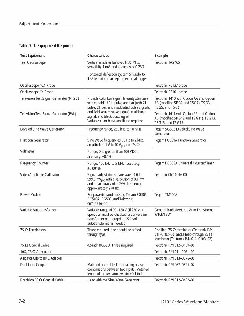
Adjustment Procedure
7–2 1710J-Series Waveform Monitors
Table 7–1: Equipment Required
Test Equipment Characteristic Example
Test Oscilloscope Vertical amplifier bandwidth 30 MHz,sensitivity 1 mV, and accuracy of 0.25%
Horizontal deflection system 5 ms/div to1 s/div that can accept an external trigger.
Tektronix TAS465
Oscilloscope 10X Probe Tektronix P6137 probe
Oscilloscope 1X Probe Tektronix P6101 probe
Television Test Signal Generator (NTSC) Provide color bar signal, linearity staircasewith variable APL, pulse and bar (with 2Tpulse, 2T bar, and modulated pulse signals,
iel sq re ve si l m lti rst
Tektronix 1410 with Option AA and OptionAB (modified SPG2 and TSG7), TSG3,TSG5, and TSG6
Television Test Signal Generator (PAL) and field square wave signal), multiburstsignal, and black burst signalVariable color burst amplitude required
Tektronix 1411 with Option AA and OptionAB (modified SPG12 and TSG11), TSG13,TSG15, and TSG16.
Leveled Sine Wave Generator Frequency range, 250 kHz to 10 MHz Tegam SG503 Leveled Sine WaveGenerator
Function Generator Sine Wave frequencies 90 Hz to 2 kHz,amplitude 0.1 V to 10 Vp-p into 75 .
Tegam FG501A Function Generator
Voltmeter Range, 0 to greater than 100 VDC;accuracy, ±0.1%
Frequency Counter Range, 100 kHz to 5 MHz; accuracy,±0.001%
Tegam DC503A Universal Counter/Timer
Video Amplitude Calibrator Signal, adjustable square wave 0.0 to999.9 mVp-p with a resolution of 0.1 mVand an accuracy of 0.05%; frequencyapproximately 270 Hz.
Tektronix 067-0916-00
Power Module For powering and housing Tegam SG503,DC503A, FG503, and Tektronix067–0916–00
Tegam TM506A
Variable Autotransformer Variable range of 90 -120 V (If 220 voltoperation must be checked, a conversiontransformer or appropriate 220 voltautotransformer is needed)
General Radio Metered Auto TransformerW10MT3W.
75 Terminators Three required, one should be a feed-through type
End-line, 75 terminator (Tektronix P/N011–0102–00) and a feed-through 75 terminator (Tektronix P/N 011–0103–02)
75 Coaxial Cable 42-inch RG59U, Three required Tektronix P/N 012–0159–00
10X, 75 Attenuator Tektronix P/N 011–0061–00
Alligator Clip to BNC Adapter Tektronix P/N 013–0076–00
Dual Input Coupler Matched bnc cable-T for making phasecomparisons between two inputs. Matchedlength of the two arms within ±0.1 inch
Tektronix P/N 067–0525–02
Precision 50 Coaxial Cable Used with the Sine Wave Generator Tektronix P/N 012–0482–00

Adjustment Procedure
1710J-Series Waveform Monitors 7–3
Table 7–1: Equipment Required (Cont.)
Test Equipment ExampleCharacteristic
50 -to-75 Minimum Loss Attenuator Tektronix P/N 011–0057–00
Parade Display Test Connector A 15-pin sub-miniature D-type connectormodified for RGB Parade input. SeeFigure 7–1.
Tektronix P/N 131–0459–00
RGB ENBRGB
staircase
YRGB/RGB Gnd
12 11 10 915 14 13
5 4 3 2 18 7 6
Figure 7–1: RGB/YRGB parade display test connector
ProcedureThis procedure covers only the adjustments. Checks other than those that mustbe made to ensure that a step is completed are in the Verification Procedure.
Allow 20 minutes of warm-up time, at normal room temperature (approximately25 C) before making any adjustments to the instrument. All test equipmentwarm-up times, as specified by the manufacturer, must also be observed toensure that all tolerances are within specification.
1. Set up the 1710J-Series Waveform Monitor front-panel controls as shown inTable 7–2.
Table 7–2: Preliminary Control Settings
Control Setting
POWER ON
INTENSITY Set to preference
FOCUS Set to preference
SCALE Set to preference
Preliminary Setup

Adjustment Procedure
7–4 1710J-Series Waveform Monitors
Table 7–2: Preliminary Control Settings (Cont.)
Control Setting
VERTICAL Position Set later
HORIZONTAL Position Set later
FILTER FLAT
REF INT
INPUT
GAIN (switch) off
MAG off
SWEEP 2 LINE
2. Connect the AC power cord to the variable autotransformer. Turn power on1710J-Series Waveform Monitor and set the autotransformer for either 110or 220 Volts.
3. Connect a composite multiburst signal to the CH B input and terminate theopposite side of the loop-through with a 75 termination.
The component to adjust is A1R99.
1. Connect the DMM negative lead to TP1 (GND) and the positive lead to W1(+5 V).
2. Adjust A1R99 (+5 V ADJ) for +5.0 V ±0.5 V. See Figure 7–2.
NOTE. The 5 V supply is the reference for all supplies in the 1710J-SeriesWaveform Monitor. Do not readjust this supply if it is within tolerance, unlessyou intend to perform a complete readjustment of the instrument.
+5 Adjust

Adjustment Procedure
1710J-Series Waveform Monitors 7–5
The component to adjust is A1R58.
1. Turn the INTENSity control fully counterclockwise.
2. Adjust A1R58 (CRT BIAS) so that the display is just extinguished.
3. Set the INTENSity control to desired level.
A3 Main board
Front
R856
C953
ÉÉÉÉÉÉÉÉÉÉÉÉÉÉÉÉÉÉÉÉÉÉÉÉÉÉÉÉÉÉÉÉÉÉÉÉÉÉÉÉÉÉÉÉÉÉÉÉÉÉÉÉÉÉÉÉÉÉÉÉÉÉÉÉÉÉÉÉÉÉÉÉÉÉÉÉÉÉÉÉÉÉÉÉÉÉÉÉÉÉÉÉÉÉÉÉÉÉÉÉÉÉÉÉÉÉÉÉÉÉÉÉÉÉÉÉÉÉÉÉÉÉÉÉÉÉÉÉÉÉÉÉÉÉÉÉÉÉÉÉÉÉÉÉÉÉÉÉÉÉ
CAUTION
MAINS
VOLTAGE
W1 +5 V
R552 R553
R755
R660 R661
R167 R168
C368 C372R274
Test point
C195
L180 L190
Q280 Q289
R489R492
C696R689
C775
C777
R700
R701 C784
C783C778 C683
R683R680
J500 J197
J699
CRTBIASR58
GEOMR45
FOCUSR11
W4 –15 VW3 +15 V
+5 VADJ*R99
*671–2890–07 and aboveA1 Power supply board
ASTIGR49
J99
R003
J504
Figure 7–2: Adjustment locations for the Main and Power Supply boards
The components to adjust are A1R45, A1R11, and A1R49.
1. Connect the DMM between pin1 of A1J3 and ground.
2. Adjust R45 (GEOM) for 35V ±1 V at pin 1 of J3.
CRT Bias
Geometry, Focus andAstigmatism

Adjustment Procedure
7–6 1710J-Series Waveform Monitors
3. Select CH B input.
4. Set the front-panel FOCUS control to approximately the center of itsrotation.
5. Adjust R11 (CENTER FOCUS) and R49 (ASTIG) for the most clearly-de-fined multiburst display.
The component to adjust is the front-panel ROTATE.
1. Select CH A input.
2. Adjust the front-panel ROTATE for a level trace across the CRT’s 0 IRE line(NTSC) or 0.3 V line (PAL).
The components to adjust are A1R167 and A1R168.
NOTE.
1. Connect the voltmeter ground lead to one of the rear-panel ground lugs andthe active lead to the –11.8 V test point. See Figure 7–3.
2. Adjust R167 (–11.8 V ADJ) for –11.78 to –11.82 V.
Trace Rotation
Main Circuit BoardRegulated Power Supplies

Adjustment Procedure
1710J-Series Waveform Monitors 7–7
Front
R167 R168U164 U172
–11.8 VTest point
+11.8 VTest point
A3 Main board
Figure 7–3: Segment of the Main board, showing the test points and adjustmentlocations for the ±11.8 V supplies
3. Connect the voltmeter active lead to the +11.8 V test point. See Figure 7–3.
4. Adjust R168 (+11.8 V ADJ) for +11.78 to +11.82 volts.
The components to adjust are A3R660 and A3R552
1. Display the CAL signal in the 2 LINE sweep.
2. Adjust R660 (Sweep Length) for one cycle of the calibrator signal per majordivision over the center ten divisions.
3. Turn on the MAG.
4. Adjust R552 (1 s Cal) for one full cycle over the ten major divisions.
The component to adjust is A1R553.
1. Set REF to INT and select CH A input.
2 Line and 1 s SweepCalibration
0.2 s Sweep Calibration
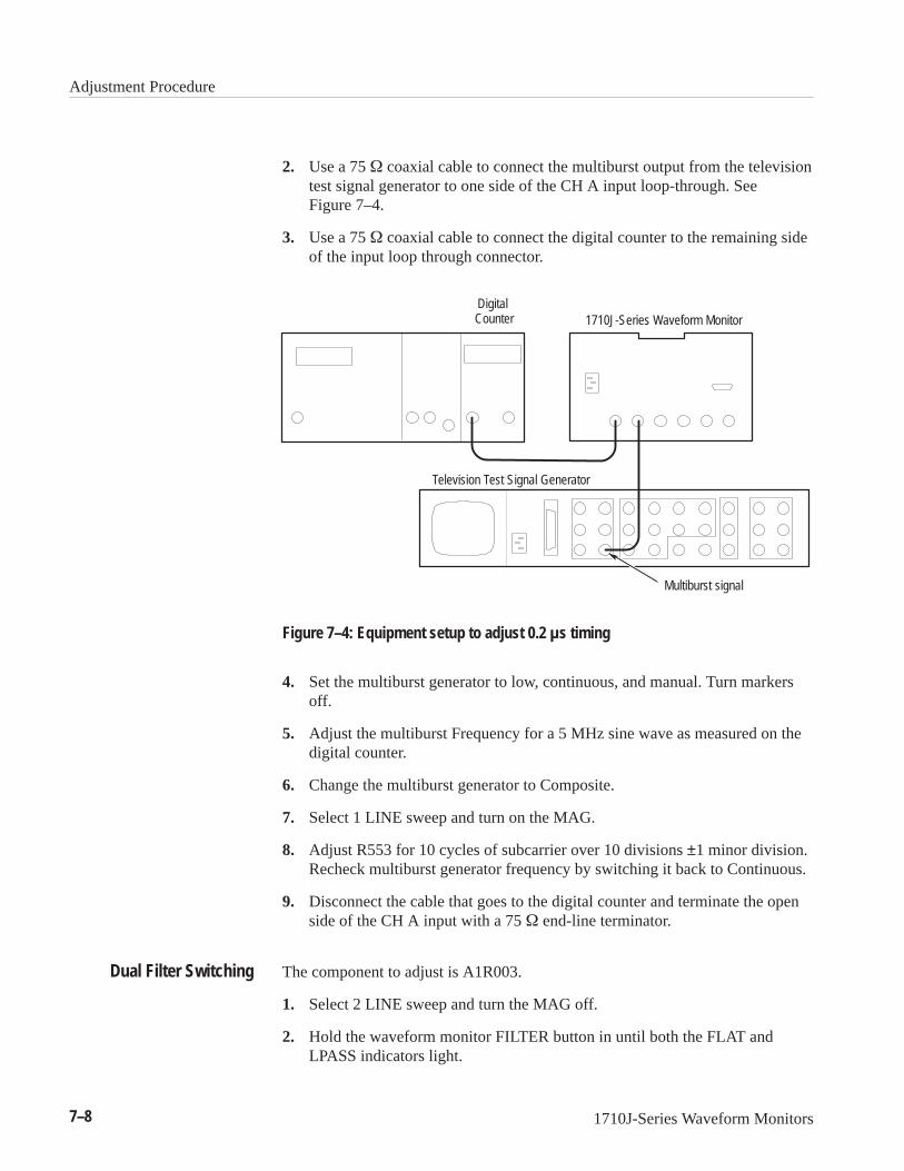
Adjustment Procedure
7–8 1710J-Series Waveform Monitors
2. Use a 75 coaxial cable to connect the multiburst output from the televisiontest signal generator to one side of the CH A input loop-through. SeeFigure 7–4.
3. Use a 75 coaxial cable to connect the digital counter to the remaining sideof the input loop through connector.
1710J-Series Waveform Monitor
Television Test Signal Generator
Multiburst signal
Digital Counter
Figure 7–4: Equipment setup to adjust 0.2 s timing
4. Set the multiburst generator to low, continuous, and manual. Turn markersoff.
5. Adjust the multiburst Frequency for a 5 MHz sine wave as measured on thedigital counter.
6. Change the multiburst generator to Composite.
7. Select 1 LINE sweep and turn on the MAG.
8. Adjust R553 for 10 cycles of subcarrier over 10 divisions ±1 minor division.Recheck multiburst generator frequency by switching it back to Continuous.
9. Disconnect the cable that goes to the digital counter and terminate the openside of the CH A input with a 75 end-line terminator.
The component to adjust is A1R003.
1. Select 2 LINE sweep and turn the MAG off.
2. Hold the waveform monitor FILTER button in until both the FLAT andLPASS indicators light.
Dual Filter Switching
Adjustment Procedure
1710J-Series Waveform Monitors 7–9
3. Position the tip of the sync pulse that occurs between the two lines so thatthe switching transition is visible.
4. Adjust R636 (Switching Phase) to placed the switching transition at thecenter of the sync tip.
The component to adjust is A1R661.
1. Set the multiburst generator for High Range Multiburst.
2. Turn on the 1710J-Series Waveform Monitor MAG.
3. Use the HORIZONTAL Position control to position the leading edge of thesync pulse to the center major graticule division.
4. Turn the MAG off.
5. Adjust R661 (MAG Reg) so that the leading edge of sync is at the centermajor graticule division. It may be necessary to repeat this step several timesto achieve magnifier registration.
6. With the MAG off, check that both ends of the trace can be positioned to atleast the center of the screen.
The component to adjust is A3R856.
1. Change from the multiburst signal to the color bar signal.
2. Set the 1710J-Series Waveform Monitor sweep to 1 LINE.
3. Set the HORIZONTAL Position control to mid range.
4. Connect pin 2 of the rear-panel REMOTE socket to ground.
5. Note that the color bar display compresses to 1/4 to 1/3 of its previouslength.
6. Adjust R856 (RGB Offset) to center the display at mid screen.
The component to adjust is A3C953.
1. Remove the color bar signal from the CH A input.
2. Use a 75 coaxial cable with the alligator clip to BNC adaptor to connectthe output of function generator to the REMOTE connector pin 1 (cablecenter conductor) and 1710J-Series Waveform Monitor chassis ground. Pin 2of the REMOTE connector should still be grounded
3. Set the function generator for a 10 V, 2 kHz square wave signal.
Magnifier Registration
RGB Offset
RGB Compensation

Adjustment Procedure
7–10 1710J-Series Waveform Monitors
4. Connect a probe from the test oscilloscope to the junction of R854 andR755. See Figure 7–2 for locations.
5. Adjust C953 (RGB Comp) for best transient response.
6. Remove the connections from the REMOTE connector.
The component to adjust is A3R489.
1. Set the VERTICAL Position control fully clockwise.
2. Connect the voltmeter lead to the collector (transistor case) of Q280. SeeFigure 7–2.
3. Adjust R489 (Limit Cent) for +0.8 V.
4. Set the VERTICAL Position control fully counterclockwise.
5. Connect the voltmeter lead to the collector (transistor case) of Q289. SeeFigure 7–2.
6. Check that the voltage is +0.8 V. If it is not, repeat steps 1 through 5 untilthe collector voltages are balanced at the same DC level.
The component to adjust is A3R689.
1. Use a 75 coaxial cable to connect the VAC signal to the 1710J-SeriesWaveform Monitor CH A input; do not terminate the remaining side of theloop-through input. See Figure 7–5.
2. Set the VAC for an output of 999.9 mV.
3. Move A3J500 (DC Restore) to the 1-2 (Off) position.
1710J-Series Waveform Monitor
Do not terminate
Video Amplitude Calibrator
Figure 7–5: Equipment setup for adjusting the calibrator amplitude
Vertical Amplifier OutputBias
Calibrator SignalAmplitude

Adjustment Procedure
1710J-Series Waveform Monitors 7–11
4. Adjust the 1710J-Series Waveform Monitor front-panel V CAL so that theVAC signal is displayed as exactly 1 Vp-p (140 IRE on the NTSC graticule)on the CRT graticule.
5. Hold the 1710J-Series Waveform Monitor REF button until the CAL signalreplaces the function generator signal on the display.
6. Adjust R689 (Cal Ampl) so that the Calibrator amplitude is 1 Vp-p (140 IRENTSC) as displayed on the CRT graticule.
The component to adjust is A3R492.
1. Use a 75 coaxial cable to connect the color bar signal through a 75
in-line terminator and a Dual Input Coupler to the 1710J-Series WaveformMonitor CH A and CH B inputs. Do not terminate the loop-through inputs.
2. Use a 75 coaxial cable to connect the black burst signal to the 1710J-Se-ries Waveform Monitor EXT REF. Terminate the remaining side of theloop-through input with a 75 terminator.
3. Set the input to BOTH (CH A and CH B).
4. Adjust R492 (DC Bal) to overlay the CH A and CH B displays.
The component to adjust is A3R274.
1. Select CH A input.
2. Use the VERTICAL Position control to position the signal blanking level onthe graticule baseline.
3. Select X5 GAIN.
4. Adjust R274 (X5 Mag) to reposition blanking level to the baseline.
5. Select GAIN off and repeat steps 2, 3, and 4 until there is no baseline shiftwhen switching between off and X5 GAIN.
The components to adjust are A3C195, A3L180, A3L190, and A3C368.
1. Use a 75 coaxial cable to connect the television test signal generatormultiburst signal through an in-line 75 termination to the CH A input. SeeFigure 7–6.
2. Use a 75 cable to connect the television test signal generator black burstsignal to the 1710J-Series Waveform Monitor EXT REF and terminate theremaining side of the loop-through input with a 75 terminator.
Dual Input DC Level
X5 Magnifier Registration
Input A Compensationand Flat Response

Adjustment Procedure
7–12 1710J-Series Waveform Monitors
Waveform Monitor
75 Feedthrough terminator75
TerminatorTelevision Test Signal
Generator
Multiburst signal
Figure 7–6: Equipment setup for adjusting Channel A input compensation
3. Set multiburst generator to Sweep, High Range, Composite, Markers, andFull Amplitude.
4. Set the 1710J-Series Waveform Monitor sweep to 2 FLD and EXT REF.
5. Adjust C195 (CH A Comp.) for flat response at 6 MHz. See Figure 7–7.
6. Check the response in the 2-4 MHz region. If it is bumped up; adjust bothL180 and L190 in a small amount (both cores should be adjusted together).If it is dipped; adjust both L180 and L190 out a small amount (both coresshould be adjusted together).
7. Repeat steps 5 and 6 until the best response to 6 MHz is achieved. You mayneed to adjust C368 (HF Comp) slightly (it affects response in the 6-8 MHzregion).
8. Disconnect the multiburst signal from the CH A input and remove the 75
termination from the remaining side of the loop-through connector.
9. Use a precision 50 cable, a 50–75 minimum loss attenuator, a 75 feed through attenuator, and the Dual Input Coupler to connect the output ofthe leveled sine wave generator to the CH A and CH B inputs.

Adjustment Procedure
1710J-Series Waveform Monitors 7–13
100
80
60
40
20
–20
–40NTSC
7.5
12.5%
0%
75%
100%2% & 4% K FACTORTek
Roll off6th Marker
Figure 7–7: Adjusting for best flat response
10. Set the leveled sine wave generator frequency to 50 kHz and adjust itsamplitude for a 100 IRE (NTSC) or 700 mV (PAL) output as displayed onthe 1710J-Series Waveform Monitor.
11. Set the leveled sine wave generator frequency to 6 MHz.
12. Adjust C195 (CH A Comp) for 100 IRE (NTSC ) or for 700 mV (PAL).
13. Set the leveled sine wave generator frequency to 3.58 MHz (NTSC ) or 4.43(PAL) and check for 100 IRE or 700 mV±2% (2 IRE or 14 mV).
14. If not in specification at 3.58 or 4.43 MHz, repeat steps 5 through 7 (as setup by steps 1 and 2).
The component to be adjusted is A3C696.
1. Select CH B input.
2. Select 2 LINE sweep.
3. Set the leveled sine wave generator frequency to 6 MHz.
4. Adjust C696 (CH B Comp) to overlay the CH A display with the CH Bdisplay.
5. Set the leveled sine wave generator frequency to 3.58 MHz (NTSC) or 4.43(PAL) and check for 100 IRE or 700 mV ±2% (2 IRE or 14 mV).
Input B Compensation
Adjustment Procedure
7–14 1710J-Series Waveform Monitors
The component to be adjusted is A3C372.
1. Select the CH A input.
2. Select X5 VERTICAL GAIN.
3. Set the sine wave generator for 50 kHz.
4. Select CH A input, EXT REF, and 1 LINE sweep.
5. Adjust the sine wave generator for a displayed amplitude of 100 IRE (or700 mV).
6. Set the sine wave generator Frequency to 3.58 MHz (NTSC) or 4.43 MHz(PAL)
7. Adjust C372 (X5 Comp) for an amplitude of 100 IRE (NTSC) or 700 mV(PAL).
8. Set the sine wave generator frequency to 6 MHz and check that displayedamplitude is still 100 IRE, ±5 IRE (NTSC) or 700 mV, ±35 mV (PAL).
Components to adjust are A3C777 and A3C3775.
1. Set the 1710J-Series Waveform Monitor sweep to 2 LINE.
2. Use a 75 coaxial cable to connect the television test signal generator colorbar signal to the CH A input. Terminate the remaining side of the loop-through input with a 75 terminator.
3. Select input A and LPASS FILTER.
4. Turn on HORIZONTAL MAG and X5 VERTICAL GAIN.
5. Adjust C777 (LPASS Filter) for minimum chrominance (minimum tracewidth on the back porch, following color burst).
6. Position the sync pulse to the baseline at center screen.
7. Adjust C775 (LPASS Filter) for the best corner on the leading edge of thesync pulse.
8. Remove the coaxial cable from the 1710J-Series Waveform Monitor CH Ainput. Leave the 75 terminator in place.
9. Use a 75 coaxial cable to connect the output of the sine wave generator tothe 1710J-Series Waveform Monitor CH A input.
10. Set the sine wave generator for 50 kHz.
11. Adjust the sine wave generator for a display amplitude of 100 IRE (NTSC)or 700 mV (PAL).
X5 Gain HF Response
Low Pass Filter

Adjustment Procedure
1710J-Series Waveform Monitors 7–15
12. Set the sine wave generator Frequency to 4.00 MHz.
13. Re-adjust C777 for minimum chrominance.
The components to adjust are A3R683 and A3C683 for NTSC instruments, orA3R680 and A3C778 for PAL instruments.
1. Use a 75 coaxial cable to connect the television test signal generator colorbar signal to the 1710J-Series Waveform Monitor CH A input.
2. Set the television test signal generator for Full Field and turn off Luminance(Y) and Setup (NTSC). Set color bar amplitude to 75%.
3. Set the 1710J-Series Waveform Monitor to CH A, CHRM FILTER, 1 LINEsweep, and sweep MAG off.
4. Adjust R683 (NTSC Chroma Filter Gain) or R680 (PAL Chroma FilterGain) so that the amplitude of the largest color packet is 100 IRE or 700 mV,depending on the color standard employed.
5. Adjust C683 (3.58 NTSC) or C778 (PAL) for the squarest envelope(minimum burst envelope decay time). It may be necessary to readjust C783(NTSC) or C784 (PAL) for maximum amplitude.
6. It may be necessary to perform steps 4 and 5 several times before reachingthe optimum setting for both Gain and Chroma Filter Compensation.
7. Move A3J500 (DC Restore) jumper to the 2-3 (On) position.
Chroma Filter

Adjustment Procedure
7–16 1710J-Series Waveform Monitors

Maintenance

1710J-Series Waveform Monitors 8–1
Maintenance
This section of the manual provides the servicing instructions for the 1710J–Se-ries Waveform Monitor. Following the Service Strategy and the precautionaryinformation there is discussion of the internal (cover off) plug jumper settings,and other installation information. The next portion of the section providesinstructions for inspection and cleaning and the step–by–step removal andreplacement procedures. The sections ends with the troubleshooting procedures.
Service StrategyThis manual contains all of the information needed for periodic maintenance ofthe 1710J–Series Waveform Monitor. All components listed in the ReplaceableElectrical and Mechanical Parts Lists can be obtained from Tektronix.
There are two Replaceable Parts Lists (electrical and mechanical) for this manualthey have a complete a list of all the components of this instrument. To isolate afailure to a component, use the troubleshooting procedures, schematic diagramsand circuit board drawings. To remove and replace any failed module, follow theRemoval and Replacement Instructions that are further back in this section.
Tektronix provides service to cover repair under warranty. Other services areavailable that may provide a cost–effective answer to your service needs.
Whether providing warranty repair service or any of the other services listedbelow, Tektronix service technicians, trained on Tektronix products, are bestequipped to service your 1710J–Series Waveform Monitor. Tektronix techniciansare appraised of the latest information on improvements to the product as well asthe latest product options.
Tektronix warrants this product for one year from the date of purchase. (Thewarranty appears after the title page and copyright page in this manual.)Tektronix technicians provide warranty service at most Tektronix servicelocations worldwide. Your Tektronix product catalog lists all service locationsworldwide.
Tektronix offers single per–incident and annual maintenance agreements thatprovide Depot Service repair of this instrument.
Of these services, the annual maintenance agreement offers a particularlycost–effective approach to service for many owners of the 1710J–SeriesWaveform Monitor. Such agreements can be purchased to span several years.
For More Information. Contact your local Tektronix service center or salesengineer for more information on any of the repair or adjustment servicespreviously described.

Maintenance
8–2 1710J-Series Waveform Monitors
PreparationThe servicing instructions that are in this manual are intended for qualifiedservice personnel.
Before initiating any maintenance activity be sure to read the Safety Summery atthe front of the manual and the Servicing Safety Summery located on the pagethat separates the operating information from the servicing information.
Operating instructions are contained in the Operating Basics section, be sure toread this section if you need more information on how the 1710J–SeriesWaveform Monitor is used.
Handling Static Sensitive ComponentsThis instrument contains electrical components that are susceptible to damagefrom static discharge. Static voltages from 1 kV to 30 kV are common inunprotected environments. Table 8–1 shows the relative static dischargesusceptibility of various semiconductor classes.
Table 8–1: Static Susceptibility
Relative Susceptibility Levels Voltage
2 ECL 200 V – 500 V
3 Schottky Signal Diodes 250 V
4 Schottky TTL 500 V
5 HF Bipolar Transistors 400 V – 600 V
6 JFET’s 600 V – 800 V
7 Linear Microcircuits 400 V – 1000 V
8 Low Power Schottky TTL 900 V
9 TTL 1200 V
Observe the following precautions to avoid damaging static–sensitive devices:
1. Minimize handling of static–sensitive components.
2. Transport and store static–sensitive components or assemblies in theiroriginal containers, on a metal rail, or on conductive foam. Label anypackage that contains static–sensitive components or assemblies.
3. Discharge the static voltage from your body by wearing a wrist groundingstrap when handling static–sensitive components. [Service assembliescontaining static–sensitive components at static–free work stations.]
Handling Precautions

Maintenance
1710J-Series Waveform Monitors 8–3
4. Remove any device capable of generating or holding a static charge from thework station surface.
5. Whenever possible keep the component leads shorted together.
6. Pick up components by the body, never by the leads.
7. Do not slide components over any surface.
8. Avoid handling components in areas where the floor or work surfacecovering is capable of generating a static charge.
9. Use a soldering iron that is connected to earth ground.
10. Use only special antistatic suction or wick–type desoldering tools.
Operating OptionsNot all installations are identical. In order to make operation of the 1710J–SeriesWaveform Monitor as flexible as possible there are internal jumpers that can bechanged to provide operating flexibility. For example, it is possible to selecteither the three–step or four–step parade to accommodate RGB or YRGBdisplays. With the exception of the 50–60 Hz jumper, the factory preset positionis indicated by a box printed on the etched circuit board. Table 8–2 details theseinternal jumper selections. If any of these jumpers are placed in the optionalposition, be sure that all operators are aware of changes to prevent unnecessarytrouble reports. See Figure 8–1 for location of the internal plug jumpers.
A3 Main board
J99Clamp enable
J197Ch A input coupling
J699Ch B input coupling
R856RGBOffset
C953RGBComp
Fron
t
Figure 8–1: Plug jumper locations and RGB compensation adjustments
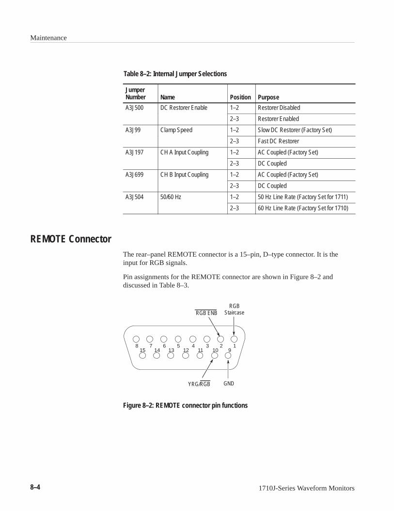
Maintenance
8–4 1710J-Series Waveform Monitors
Table 8–2: Internal Jumper Selections
JumperNumber Name Position Purpose
A3J500 DC Restorer Enable 1–2 Restorer Disabled
2–3 Restorer Enabled
A3J99 Clamp Speed 1–2 Slow DC Restorer (Factory Set)
2–3 Fast DC Restorer
A3J197 CH A Input Coupling 1–2 AC Coupled (Factory Set)
2–3 DC Coupled
A3J699 CH B Input Coupling 1–2 AC Coupled (Factory Set)
2–3 DC Coupled
A3J504 50/60 Hz 1–2 50 Hz Line Rate (Factory Set for 1711)
2–3 60 Hz Line Rate (Factory Set for 1710)
REMOTE ConnectorThe rear–panel REMOTE connector is a 15–pin, D–type connector. It is theinput for RGB signals.
Pin assignments for the REMOTE connector are shown in Figure 8–2 anddiscussed in Table 8–3.
RGB ENB
YRG/RGB GND
RGBStaircase
123456789101112131415
Figure 8–2: REMOTE connector pin functions

Maintenance
1710J-Series Waveform Monitors 8–5
Table 8–3: Remote Connector Pin Assignments and Functions
Pin Name Function/Description
1 RGB Staircase The RGB Staircase input signal controls the internalsweep ramp to offset the Horizontal in time with theRGB PARADE signal.
2 RGB Enable Low = RGB Enable. Level sensitive, allows theinstrument to process the RGB staircase input.
9 Ground Instrument ground for Remote Control
A TTL low level (ground) on pin 2 of the REMOTE connector enables theshortened RGB/YRGB sweep. A 10 V square wave input to pin 1 providesapproximately nine divisions of sweep. This sweep can be either one line or onefield depending on front–panel switch setting. The displayed signal is thefront–panel selected CH A or CH B input.
When the 1710J–Series Waveform Monitor is substituted for a Tektronix 528 or528A Waveform Monitor, in some applications the +28 V enable signal used bythe 528 must be converted to ground closure (0 VDC). This conversion requiresonly a few common parts, as shown in Figure 8–3.
+28VEnabling
voltage
47K0.25W
1N415230V
150mA
3K0.25W
2N3904 To 1/10J–SeriesREMOTE connector
Figure 8–3: Common parts used to convert from +28 Vdc enable to ground closure
RGB Offset and Compensation. Television cameras vary in output dc level; R856is provided to compensate for this variation in dc level. See Figure 8–1.
C953 is the input compensation that matches the Staircase Amplifier input timeconstant to the camera output time constant. See Figure 8–1.
Each time the camera input to the 1710J–Series Waveform Monitor is changed,the RGB offset and input time constant will probably need to be reset. Thefollowing procedure provides a simple means to make these adjustments.
The RGB offset adjustment sets the display in the useable part of the 1710J–Se-ries Waveform Monitor graticule. The following procedure is easy to performand requires no special test equipment.
RGB/YRGB ParadeDisplay
Setting RGB Offset

Maintenance
8–6 1710J-Series Waveform Monitors
1. Display any standard television waveform. Do not enable the rear–panelREMOTE connector RGB enable.
2. Use the 1710J–Series Waveform Monitor HORIZONTAL position control toalign the display with the graticule.
3. Ground the REMOTE connector RGB Enable (pin 2) and apply the camerastaircase output to the RGB Staircase input (pin 1).
4. Apply the camera video output to the 1710J–Series Waveform MonitorINPUT (CH A or CH B) and select that input with the front–panel INPUTswitch.
5. Adjust R856 (see Figure 8–1 for location) to center the RGB signal on thegraticule.
6. Adjust C953 for the best looking display.
Preventive MaintenancePreventive maintenance consists of cleaning, visual inspection, performancechecking, and, if needed, readjustment. The preventive maintenance scheduleestablished for the instrument should be based on the environment in which it isoperated and the amount of use. Under average conditions, scheduled preventivemaintenance should be performed every 2000 hours of operation.
Cleaning and InspectionPreventive maintenance consists of cleaning and visual inspection. The scheduledepends on the severity of the operating environment. Under average conditions,perform preventive maintenance after 2000 hours of operation.
Clean the entire instrument often enough to prevent dust and dirt from accumu-lating. Dirt can act as a thermal insulating blanket that prevents effective heatdissipation. In addition, dust buildup can provide high–resistance electricalleakage paths between conductors or components in a humid environment.
Exterior. Cleaning the exterior consists of an occasional wiping of the outsidesurfaces with a damp soft cloth. Do not use commercial cleaners because theycould discolor or damage the finish.
Check all air vents on a regular schedule to ensure that there is not a dust buildupthat could impede the flow of cooling air.
Cleaning
Maintenance
1710J-Series Waveform Monitors 8–7
WARNING. To avoid any potential of electrical shock, disconnect power beforeremoving the instruments cabinet.
CRT. Clean the CRT protective shield, light filter, and CRT face with a soft,lint-free cloth dampened in denatured alcohol.
Interior. Interior cleaning is not recommended, but if it is necessary, uselow-velocity, dry air to blow away dust or lint. If air alone does not remove all ofthe dust and lint, use a soft brush to complete the task. Exercise extreme care tonot disturb components on the plug-in circuit boards during cleaning.
CAUTION. This instrument contains static sensitive devices that can be damagedby static discharge. Wear a wrist grounding strap when working on thisinstrument’s circuitry.
CAUTION. Do not allow water to get inside any enclosed assembly or component.Do not clean any plastic materials with organic cleaning solvents, such asbenzene, toluene, xylene, acetone, or similar compounds, because they maydamage the plastic.
After cleaning, carefully check the instrument for defective connections,damaged parts, and improperly seated transistors or integrated circuits. Theremedy for most visible defects is obvious; however, if heat–damaged parts arediscovered, determine the cause of overheating before replacing the damagedpart, to prevent additional damage.
Periodic checks of the transistors and integrated circuits are not recommended.The best measure of performance is the actual operation of the component in thecircuit.
Instrument performance should be checked after each 2000 hours of operation orevery 12 months, if used intermittently. This will help to ensure maximumperformance and assist in locating defects that may not be apparent duringregular operation.
Visual Inspection
Performance Verificationand Readjustment

Maintenance
8–8 1710J-Series Waveform Monitors
Removal and Replacement InstructionsThe instructions contained here are for disassembly. Reassembly is performed byreversing the order of the steps used to disassemble the instrument.
WARNING. To avoid possible electrical shock, disconnect the power cord beforereplacing components.
CAUTION. To avoid potential short circuiting do not reinsert screws in the rearpanel when the instrument is removed from the cabinet.
CAUTION. To avoid short circuiting potential, do not install cabinet mountingscrews when the instrument is out of the cabinet.
NOTE. All screws, unless otherwise noted, are TORX _ screws and can beremoved with a T15 screwdriver tip (Tektronix part number 003–0966–00). Theexception is #2 Pozidrive _ screws which can be removed with a #1 Pozidrive tip(Tektronix part number 003–0443–00).
In order to replace the graticule light bulbs, clean or replace the CRT, or removethe instruments front panel it is necessary to remove the CRT bezel. Removalrequires a screwdriver with a T15 Torx tip.
1. Remove the two bezel screws. See Figure 8–4.
2. Grasp the bottom of the bezel and pull straight out and upward. There aretwo hinges at the top of the bezel that hold it in place; once the bezel is at anapproximate 45 angle with the front panel they will disengage.
To replace the graticule bezel perform the following steps:
1. Engage the bezel top tabs with the hinge slots.
2. Allow the bezel to hinge down till it sits flat with the front panel.
3. Reinstall the two bezel screws. See Figure 8–4.
Bezel Removal
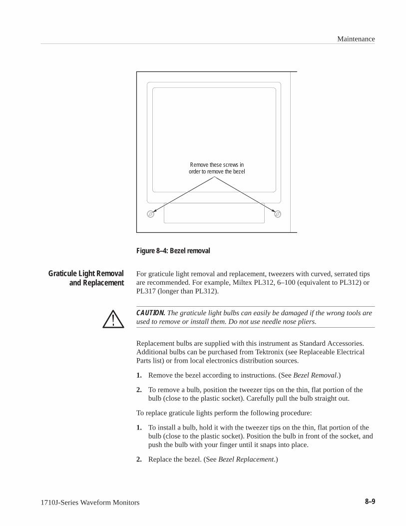
Maintenance
1710J-Series Waveform Monitors 8–9
Remove these screws inorder to remove the bezel
Figure 8–4: Bezel removal
For graticule light removal and replacement, tweezers with curved, serrated tipsare recommended. For example, Miltex PL312, 6–100 (equivalent to PL312) orPL317 (longer than PL312).
CAUTION. The graticule light bulbs can easily be damaged if the wrong tools areused to remove or install them. Do not use needle nose pliers.
Replacement bulbs are supplied with this instrument as Standard Accessories.Additional bulbs can be purchased from Tektronix (see Replaceable ElectricalParts list) or from local electronics distribution sources.
1. Remove the bezel according to instructions. (See Bezel Removal.)
2. To remove a bulb, position the tweezer tips on the thin, flat portion of thebulb (close to the plastic socket). Carefully pull the bulb straight out.
To replace graticule lights perform the following procedure:
1. To install a bulb, hold it with the tweezer tips on the thin, flat portion of thebulb (close to the plastic socket). Position the bulb in front of the socket, andpush the bulb with your finger until it snaps into place.
2. Replace the bezel. (See Bezel Replacement.)
Graticule Light Removaland Replacement

Maintenance
8–10 1710J-Series Waveform Monitors
The CRT is a high–vacuum device and you need to be cautious about how it isremoved and handled. When handling a CRT always wear safety glasses and ifpossible, wear gauntlet type leather gloves for its transportation. Always storeCRTs in protective packaging; do not leave a CRT sitting on a bench top or desk.
1. Remove the bezel. (See Bezel Removal.)
2. Remove the CRT protective filter.
WARNING. The CRT may retain a dangerous charge. Ground the conductor of theanode to discharge the CRT. Do not allow the conductor to touch your body orany circuitry.
3. Slide a screwdriver with an insulated handle under the anode cap on the sideof the CRT, and ground the anode to the chassis, to discharge the CRT. DONOT touch the metal shaft of the screwdriver while doing this. Disconnectthe anode cap by prying it gently away from the CRT.
4. Disconnect J225 (trace rotation) on the Main board and push the connectorthrough the hole in the board.
5. The CRT can now be pulled straight out (some pressure may be needed). TheCRT shield, along with the grommet around its front and the rubber manchetaround its back, should come out with the CRT.
To replace the CRT perform the following procedure:
1. If the CRT is to be replaced, remove the metal shield from the neck of theold CRT and place it around the neck of the new CRT, with the WARNINGsticker towards the top of the instrument. This should place the opening inthe grommet on the front edge of the shield towards the bottom of theinstrument. Ensure that the rubber manchet is on the back edge of the shield.
2. Slip the CRT part way back into position and feed the trace rotation wires(and plug) back through the hole in the Main board.
WARNING. The CRT may retain a dangerous charge. Ground the the anodeconnector to discharge the CRT. Do not allow the conductor to touch your bodyor any circuitry.
3. Use a screwdriver to ground the anode connector on the CRT to the chassis.
4. Slide the CRT into the instrument, guiding the rubber manchet on the end ofthe shield into the rear CRT support.
5. Align the socket on the A10 CRT Socket board with the pins and key on theCRT. Gently push the CRT and the socket board together until the CRT pinsare fully seated in the socket.
CRT Removal andReplacement
Maintenance
1710J-Series Waveform Monitors 8–11
6. Replace the trace rotation connector (J255, Main board), and snap the anodelead onto the anode connector on the side of the CRT.
7. Wipe the faceplate of the CRT to remove fingerprints, then replace the bezel.If the fit is too tight to allow the bezel to go into position, or if the CRT has aloose fit after the bezel is completely tightened down, then the rear CRTsupport must be repositioned.
To reposition the rear CRT support, loosen the two nuts that hold the supportin place. With the CRT and bezel in place, push the support towards the frontof the instrument until it is snug against the rubber manchet on the rear ofthe CRT shield. Tighten the two support nuts.
The rear panel is mounted directly to the main chassis. It is held in place withthree Torx head screws. In addition, the instruments power plug is mounted onthe rear panel with two additional Torx head screws. Use a screwdriver with aT15 Torx tip to remove and replace the rear panel.
1. Remove the five rear screws. See Figure 8–5.
2. Unsolder the lead to the six BNC connectors and one the one groundconnection.
3. Pull the rear panel free from the chassis; be careful not to pull the unsolderedwires.
To replace the rear panel perform the following procedure:
1. Hold the rear panel in place and replace the three screws holding it to themain chassis.
2. Resolder the connections to the six BNC connectors and the ground wire.
3. Reinstall the screws holding the instruments power connector to the rearpanel.
Removing the Rear Panel

Maintenance
8–12 1710J-Series Waveform Monitors
AUXILIARY CONTROL
Remove these five (5)screws to remove the rear panel.
Figure 8–5: Rear panel securing screws
The instrument’s front–panel circuit board is mounted on the back of the frontpanel. It is necessary to remove this assembly in order to access the front panelswitches and controls. There are two Torx head screws that fasten the front panelto front casting. The circuit board is mounted to front panel with four Torx headscrews. Use a screwdriver with a T15 Torx tip to remove and replace these items.
1. Remove the blue multi–wire connector from J154.
2. Remove the two screws holding the board in place. See Figure 8–6.
3. Remove the board by slipping it through the front–panel opening.
4. To access the Front Panel board components:
a. Remove the knobs from the front.
b. Remove the four screws from the rear.
c. The board should now separate from the front panel for componentaccess.
To replace the front panel and front panel circuit board perform the followingprocedure:
1. Push the circuit board switch buttons and control knobs through theirrespective holes in the front panel.
2. Replace the four screws that fasten the circuit board to the front panel.
Front Panel andFront Panel Circuit Board
Removal

Maintenance
1710J-Series Waveform Monitors 8–13
3. Replace the front–panel knobs.
4. Carefully slide the circuit board through the front–panel opening.
5. Replace the two screws holding the front panel to the front casting.
6. Replace the multi–wire connector on J154.
To remove frontpanel assembly
To remove frontpanel assembly
To separate boardfrom the front panel
Figure 8–6: Screws that hold the front panel circuit board (A2) in place
The main circuit board is held in place by eight Torx head screws. Use ascrewdriver with a T15 Torx tip to remove and replace these screws. In additiona soldering iron is required to remove this circuit board.
1. Remove the plugs from the following connectors: J107 to the Front Panelboard, J4 on the Power Supply board, and J225 on the Main board (the tracerotation leads to the CRT).
2. Unsolder the leads to the six BNC connectors and three ground from the rearpanel, the two horizontal CRT leads (red and green), and the two verticalCRT leads (blue and brown).
Removing the Main Board

Maintenance
8–14 1710J-Series Waveform Monitors
3. Slip the CRT and trace rotation leads through the appropriate holes in theMain board.
4. Remove the eight screws that are holding the board in place. See Figure 8–7for their locations.
J107J154
J932
A3 Main BdFr
ont
Figure 8–7: Screws holding the Main circuit board (A3) in place
5. Remove the board by sliding it toward the rear panel until the toe of theboard clears the front, then lift out.
To replace the main circuit board perform the following procedure:
1. To replace the Main board, lay the board flat and slide it forward into place.
2. Reinstall the eight screws that hold the circuit board in place.
3. Slip the CRT and trace rotation leads through the appropriate holes in theMain board and reconnect them.
4. Solder the leads to the six BNC connectors and three grounds from the rearpanel, the two horizontal CRT leads (red and green), and the two verticalCRT leads (blue and brown).
5. Reinstall the plugs on the following connectors: J107 to the Front Panelboard, J4 on the Power Supply board, and J225 on the Main board (the tracerotation leads to the CRT).
The front–panel power switch is held in place with two Pozidrive[ screws. Use ascrewdriver with a #1 Pozidrive tip to remove and replace these screws
The circuit board is held in place with seven Torx head screws. In addition, thepower line filter is held in place on the rear panel with two Torx head screws.Use a screwdriver with a T15 Torx tip to remove and replace them.
Removing thePower Supply Board
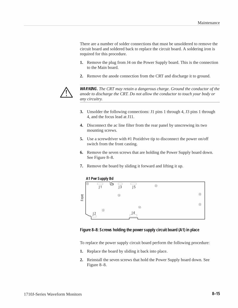
Maintenance
1710J-Series Waveform Monitors 8–15
There are a number of solder connections that must be unsoldered to remove thecircuit board and soldered back to replace the circuit board. A soldering iron isrequired for this procedure.
1. Remove the plug from J4 on the Power Supply board. This is the connectionto the Main board.
2. Remove the anode connection from the CRT and discharge it to ground.
WARNING. The CRT may retain a dangerous charge. Ground the conductor of theanode to discharge the CRT. Do not allow the conductor to touch your body orany circuitry.
3. Unsolder the following connections: J1 pins 1 through 4, J3 pins 1 through4, and the focus lead at J11.
4. Disconnect the ac line filter from the rear panel by unscrewing its twomounting screws.
5. Use a screwdriver with #1 Pozidrive tip to disconnect the power on/offswitch from the front casting.
6. Remove the seven screws that are holding the Power Supply board down.See Figure 8–8.
7. Remove the board by sliding it forward and lifting it up.
A1 Pwr Supply Bd
J4J2
J1 J3
Fron
t
J5
Figure 8–8: Screws holding the power supply circuit board (A1) in place
To replace the power supply circuit board perform the following procedure:
1. Replace the board by sliding it back into place.
2. Reinstall the seven screws that hold the Power Supply board down. SeeFigure 8–8.

Maintenance
8–16 1710J-Series Waveform Monitors
3. Use a screwdriver with #1 Pozidrive tip to reinstall the power on/off switchto the front casting.
4. Reconnect the AC line filter from the rear panel by reinstalling the twomounting screws.
5. Solder the following connections: J1 pins 1 through 4, J3 pins 1 through 4,and the focus lead at J11.
6. Reconnect the anode connection to the CRT.
7. Reconnect the plug on J4.
TroubleshootingThe material at the start of this discussion is general and is not intended to coverspecific cases. Note that the manual itself is considered a troubleshooting aid,and as such a brief discussion of its content is in order.
The procedural information that appears as “General Troubleshooting Tech-niques” should be familiar to most technicians; however, a quick review maysave some time and reduce “wheel spinning.”
The instructions for troubleshooting the low voltage power supply are detailed.These instructions should be followed to the letter in order to accomplish thetask.
The foldout pages at the back of the manual contain information that is useful introubleshooting the instrument. Block and schematic diagrams, circuit boardillustrations, and parts locating charts are found there.
Diagrams. Schematic diagrams are the most often used troubleshooting aids. Thecircuit number and electrical value of each component is shown on the diagram.The first page has definitions of the symbology used on the schematic diagrams.Refer to the Replaceable Electrical Parts list for a complete description of eachcomponent. Circuits that are mounted on circuit boards or assemblies areenclosed in a border, with the name and assembly number shown on the border.
Circuit Board Illustrations. Electrical components, connectors, and test points areidentified on circuit board illustrations, which are located on the page facing thefirst schematic diagram for that board. Circuit board illustrations are assignedlocation grids along the left side and top, which are used with the parts locatingcharts to rapidly locate the components.
Foldout Pages
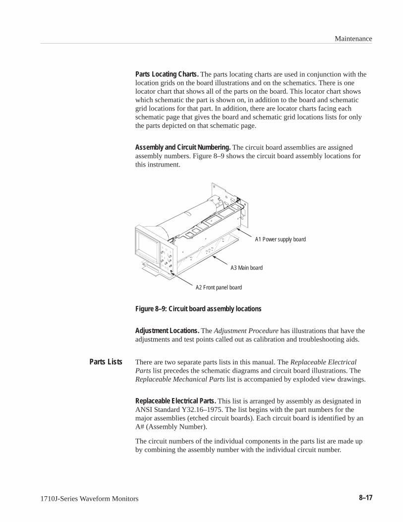
Maintenance
1710J-Series Waveform Monitors 8–17
Parts Locating Charts. The parts locating charts are used in conjunction with thelocation grids on the board illustrations and on the schematics. There is onelocator chart that shows all of the parts on the board. This locator chart showswhich schematic the part is shown on, in addition to the board and schematicgrid locations for that part. In addition, there are locator charts facing eachschematic page that gives the board and schematic grid locations lists for onlythe parts depicted on that schematic page.
Assembly and Circuit Numbering. The circuit board assemblies are assignedassembly numbers. Figure 8–9 shows the circuit board assembly locations forthis instrument.
A2 Front panel board
A3 Main board
A1 Power supply board
Figure 8–9: Circuit board assembly locations
Adjustment Locations. The Adjustment Procedure has illustrations that have theadjustments and test points called out as calibration and troubleshooting aids.
There are two separate parts lists in this manual. The Replaceable ElectricalParts list precedes the schematic diagrams and circuit board illustrations. TheReplaceable Mechanical Parts list is accompanied by exploded view drawings.
Replaceable Electrical Parts. This list is arranged by assembly as designated inANSI Standard Y32.16–1975. The list begins with the part numbers for themajor assemblies (etched circuit boards). Each circuit board is identified by anA# (Assembly Number).
The circuit numbers of the individual components in the parts list are made upby combining the assembly number with the individual circuit number.
Parts Lists
Maintenance
8–18 1710J-Series Waveform Monitors
Example: R117 on Assembly (circuit board) A3 would be listed in the Replace–able Electrical Parts list as A3R117.
NOTE. Always consult the parts list for part numbers and descriptions whenordering replacement parts. Some parts may have been replaced or have adifferent part number in an individual instrument.
Replaceable Mechanical Parts. This list is arranged so that it corresponds to theexploded view drawing for major instrument components. The list and explodedview drawing follow the schematic diagrams in this manual. Standard Accesso-ries, which are also included in the parts list, are also in the exploded viewdrawing.
Signals and power supply voltages are passed through the instrument with asystem of interconnecting cables. The connector holders, on these cables, havenumbers that identify terminal connectors; numerals are used from pin 2 up. Atriangular key symbol is used to identify pin 1 on the circuit board to assist inaligning connector with correct square pins. Figure 8–10 shows the numberingscheme (and the triangular marking) on the etched circuit board.
Major AssemblyInterconnection

Maintenance
1710J-Series Waveform Monitors 8–19
CKT Bd mounted pins
Moveable 10–pin plug
Square pin connector onpower supply CKT bd
Pin 1
24 and 34 pin CKT bd connectors on Main CKT Board
Row ARow B
Pin 1
Row ARow B
Pin 1
Figure 8–10: Multiple pin connectors
The following procedure is designed to assist in isolating problems, which inturn expedites repairs and minimizes down time.
1. Ensure that the malfunction exists in the instrument. This is done by makingsure that the instrument is operating as intended by Tektronix (see OperatingBasics), and by checking that a malfunction has not occurred up stream fromthe waveform monitor.
2. Determine and evaluate all trouble symptoms. This is accomplished byisolating the problem to a general area such as an assembly. The blockdiagram is a valuable aid in signal tracing and circuit isolation.
General TroubleshootingTechniques

Maintenance
8–20 1710J-Series Waveform Monitors
CAUTION. Use extreme care when probing with meter leads or probes, because ofthe high component density and limited access within the instrument. Theinadvertent movement of leads or a probe could cause a short circuit or transientvoltages capable of destroying components.
3. Determine the nature of the problem. Attempt to make the determination ofwhether the instrument is out of calibration or if there has been a componentfailure. Once the type of failure has been determined, proceed on to identifythe functional area most likely at fault.
4. Visually inspect the suspect assembly for obvious defects. Most commonlythese will be broken or loose components, improperly seated components,overheated or burned components, chafed insulation, etc. Repair or replaceall obvious defects. In the case of overheated components, determine thecause of overheating and correct the cause before re-applying power.
5. Use successive electrical checks to locate the source of the problem. Theprimary tool for problem isolation is the oscilloscope. Use the PerformanceCheck Procedure to determine if a circuit is operating within specifications.At times it may be necessary to change a calibration adjustment to determineif a circuit is operational, but since this can destroy instrument calibration,care should be exercised. Before changing an adjustment, note its position sothat it can be returned to its original setting.
6. Determine the extent of the repair. If the necessary repair is complex, it maybe advisable to contact your local Tektronix field office or representativebefore continuing. If the repair is minor, such as replacing a component, seethe parts list for replacement information. Removal and replacementprocedures for the assemblies can be found under Corrective Maintenance.
CAUTION. Always remove the assembly from the instrument prior to attemptingto replace a soldered in component. See Corrective Maintenance for the correctprocedure.
Specific Troubleshooting TechniquesThe 1710J–Series Waveform Monitor has one area, the low voltage powersupply, where ordinary troubleshooting techniques do not apply.
The power supply is of the high–efficiency type and requires a specific trouble–shooting procedure and an isolation transformer to avoid personal danger orinstrument damage.
Power SupplyTroubleshooting
Maintenance
1710J-Series Waveform Monitors 8–21
The power supply presents special troubleshooting problems, if a fault occurs.Besides having a sizeable area where dangerous potentials can be contacted, thetype of circuitry employed can not be troubleshot by conventional means.
WARNING. Dangerous voltages exist in this power supply. Do not attempt totroubleshoot the 1710J–Series Waveform Monitor power supply without readingthese instructions.
It is important that you follow these instructions when troubleshooting thispower supply, because it can not be evaluated using traditional power supplytroubleshooting techniques.
NOTE. A review of the power supply Theory of Operation is recommended beforeattempting repairs.
The equipment needed to troubleshoot the power supply:
A Digital Multimeter (DMM), with a diode check function
A general purpose oscilloscope
A 0 to 20 VDC Variable Power Supply
A clip lead to short across a component
A high voltage probe, 1 G input resistance
The Troubleshooting Procedure for the power supply (Assembly A1) is split intotwo sections, the low volts and high volts supplies. Start the procedure bydetermining which section of the power supply has malfunctioned. Apply ACpower and turn on the power supply. From Table 8–4, determine which symptomthe power supply exhibits and refer to the corresponding procedure.
Table 8–4: Power Supply Fault Symptoms
Symptom Procedure
Line fuse open Rectifier/Switcher Check (Low Volts)
Power Supply cycles OFF/ON Output Check (Low Volts) or High VoltageOscillator Check (High Volts)
Does not power up Control Circuit Check (Low Volts)
+5 V not regulating Error Amplifier Check (Low Volts)
Improper CRT display High Volts Supply
Power SupplyTroubleshooting
Procedure
Introduction

Maintenance
8–22 1710J-Series Waveform Monitors
Low Voltage Power SupplyFaults in the low voltage supply can only be isolated using the followingprocedure.
This procedure is used to eliminate some of the more obvious faults.
1. A properly functioning and loaded low volts supply will output the voltageslisted in Table 8–5. Use the DMM to measure the voltages between TP1 andthe voltage test points. If the supply is not regulating properly, continue withthe procedure.
Table 8–5: Low Volts Supply Voltages
Test Point Voltage Range
W1 (+5 V) +4.88 to +5.12 V
W4 (+15 V) +14.0 to +16.0 V
W3 (–15 V) –14.0 to –16.0 V
W2 – (+40 V) +39.0 to +41.0 V
NOTE. The Low Volts power supply troubleshooting is performed withoutapplying AC power.
2. Disconnect AC power from the instrument. Disconnect the instrument fromthe Power Supply by removing the jumper from J4.
3. Use the DMM to measure the voltage between TP2 and the tab (drain) ofQ9. Check that the voltage is near 0 V.
WARNING. Do not proceed until the the drain of Q9 is near 0 V. Dangerousvoltage potentials are present in the circuit until the capacitors discharge.
This is a resistance check for the switcher FET and the rectifier diodes.
1. Use the DMM to measure the voltage between TP2 and the tab (drain) ofQ9. Be sure the voltage is near 0 V before proceeding.
2. Unsolder and lift one end of R102.
3. With the negative lead of the DMM connected to TP2 and the positive leadconnected to the tab of Q9, measure the circuit resistance. A resistance of
Preliminary Checks
Rectifier/Switcher Check
Maintenance
1710J-Series Waveform Monitors 8–23
less than 20 k indicates a shorted MOSFET (Q9). If the MOSFET isshorted, replace it and perform the Control Circuit Check.
4. Using the DMM diode test function, test CR21, CR22, CR23, and CR24 forshorts. Diode replacements must be fast reverse recovery (300 ns) types toreduce conducted noise.
5. Reconnect the lifted end of R102.
This procedure uses the variable power supply to check output voltages.
1. Connect the negative output from the 20 VDC power supply to TP1.Connect the positive output to W4 (+15 V). The circuit should draw lessthan 20 mA. Excessive current draw can be caused by CR11 or U2 (HighVolts power supply).
2. Connect the negative output from the 20 VDC power supply to TP1.Connect the positive output to W2 (+40 V). The circuit should draw lessthan 20 mA. Excessive current draw can be caused by CR14 or Q6 (highvolts power supply).
3. Connect the positive output from the 20 VDC Power Supply to TP1.Connect the negative output to W3 (–15 V). The circuit should draw lessthan 20 mA. Excessive current draw can be caused by CR12.
4. Connect the negative output from the 5 VDC power supply to TP1. Connectthe positive output to W1 (+5 V). The circuit should draw less than 20 mA.Excessive current draw can be caused by CR13 or Q1 and Q2 (high voltspower supply).
This procedure uses the variable power supply and an oscilloscope to determineif the control circuit is functioning properly.
1. Connect the negative output from the 20 VDC Power Supply to TP2.Connect the positive output to the cathode of CR17. Short C47 with a cliplead. Connect the oscilloscope probe ground to TP2.
2. Table 8–6 lists the signal present in a properly functioning control circuit.
Table 8–6: Control Circuit Test Points
Circuit Location Signal
U5, pin 1 Approximately 5 VDC
U5, pin 2 Approximately 2 VDC
U5, pin 3 0 V
U5, pin 4 80 kHz triangle wave, 2 V p–p
Output Check
Control Circuit Check
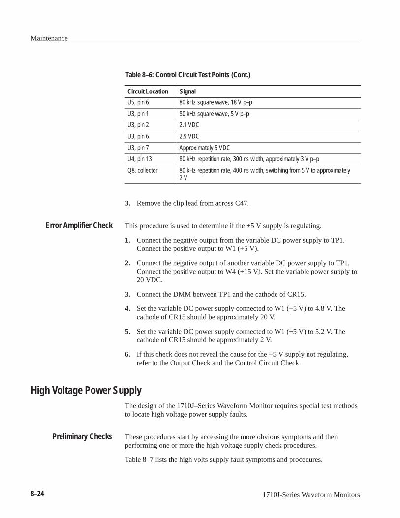
Maintenance
8–24 1710J-Series Waveform Monitors
Table 8–6: Control Circuit Test Points (Cont.)
Circuit Location Signal
U5, pin 6 80 kHz square wave, 18 V p–p
U3, pin 1 80 kHz square wave, 5 V p–p
U3, pin 2 2.1 VDC
U3, pin 6 2.9 VDC
U3, pin 7 Approximately 5 VDC
U4, pin 13 80 kHz repetition rate, 300 ns width, approximately 3 V p–p
Q8, collector 80 kHz repetition rate, 400 ns width, switching from 5 V to approximately2 V
3. Remove the clip lead from across C47.
This procedure is used to determine if the +5 V supply is regulating.
1. Connect the negative output from the variable DC power supply to TP1.Connect the positive output to W1 (+5 V).
2. Connect the negative output of another variable DC power supply to TP1.Connect the positive output to W4 (+15 V). Set the variable power supply to20 VDC.
3. Connect the DMM between TP1 and the cathode of CR15.
4. Set the variable DC power supply connected to W1 (+5 V) to 4.8 V. Thecathode of CR15 should be approximately 20 V.
5. Set the variable DC power supply connected to W1 (+5 V) to 5.2 V. Thecathode of CR15 should be approximately 2 V.
6. If this check does not reveal the cause for the +5 V supply not regulating,refer to the Output Check and the Control Circuit Check.
High Voltage Power SupplyThe design of the 1710J–Series Waveform Monitor requires special test methodsto locate high voltage power supply faults.
These procedures start by accessing the more obvious symptoms and thenperforming one or more the high voltage supply check procedures.
Table 8–7 lists the high volts supply fault symptoms and procedures.
Error Amplifier Check
Preliminary Checks

Maintenance
1710J-Series Waveform Monitors 8–25
Table 8–7: High Volts Supply Fault Symptoms
Symptom Procedure
Unable to focus CRT using the front–panelcontrol
Focus Amplifier Check
Unable to adjust CRT intensity using thefront–panel control
Z–Axis Amplifier Check, Grid Drive Check
No CRT display High Voltage Oscillator Check, CRT VoltageCheck
Before proceeding with the remainder of these procedures load the low voltssupply with the instrument or with the 20 2 W resistor from W1 to TP1.
This is the procedure to use if you cannot adjust CRT focus with the front panelfocus control.
1. Unsolder and lift one end of R24.
2. Power up the power supply.
3. Using the digital multimeter, measure the voltage between TP1 and thecollector of Q1. It should be approximately –140 V.
4. Power down the power supply.
5. Reconnect the lifted end of R24.
This is one of the two procedures to use if you cannot adjust CRT intensity withthe front panel intensity control.
1. Unsolder and lift one end of R8.
2. Power up the power supply.
3. Using the digital multimeter, measure the voltage between TP1 and thecollector of Q4. It should be approximately +10 V.
4. Short together the base and emitter of Q5. The collector of Q4 should beapproximately +100 V.
5. Power down the power supply.
6. Reconnect the lifted end of R8.
This is the other procedure to use if the front panel intensity control is notworking correctly.
Focus Amplifier Check
Z–Axis Amplifier Check
Grid Drive Check
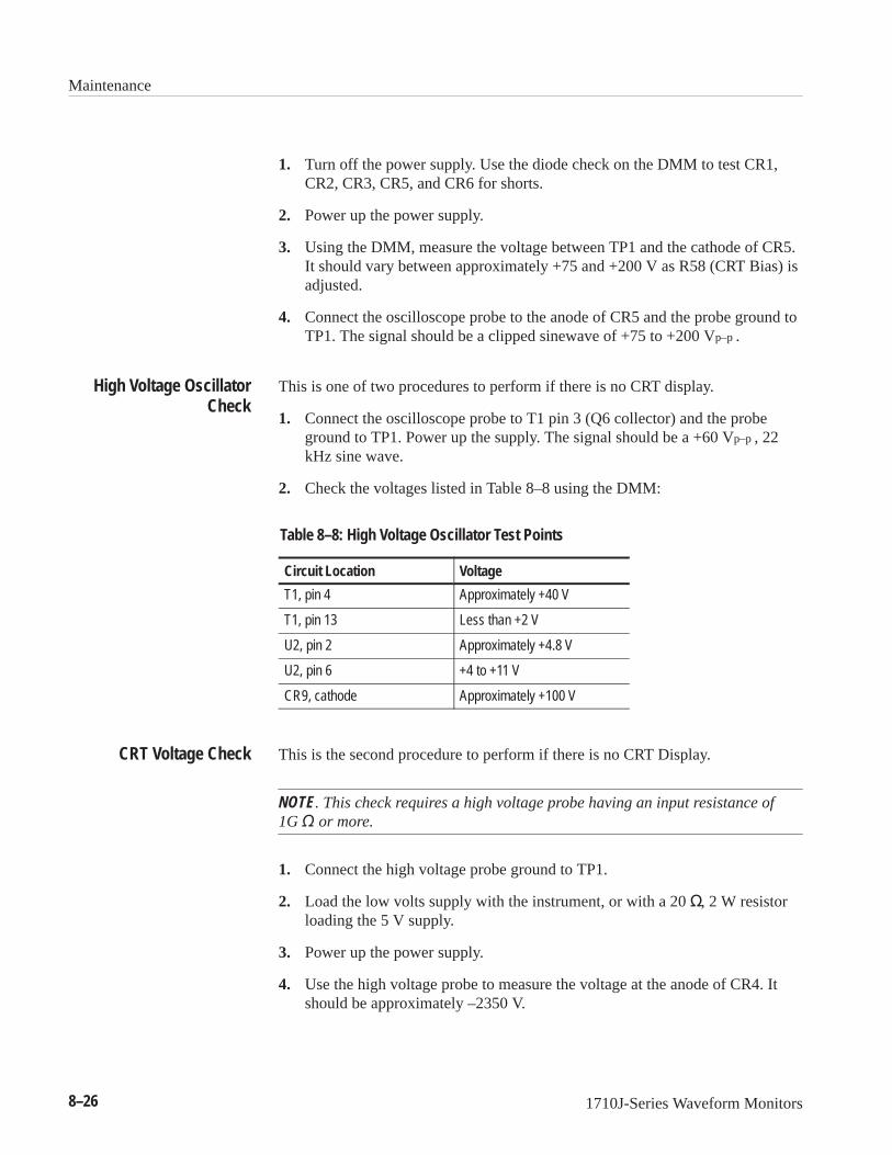
Maintenance
8–26 1710J-Series Waveform Monitors
1. Turn off the power supply. Use the diode check on the DMM to test CR1,CR2, CR3, CR5, and CR6 for shorts.
2. Power up the power supply.
3. Using the DMM, measure the voltage between TP1 and the cathode of CR5.It should vary between approximately +75 and +200 V as R58 (CRT Bias) isadjusted.
4. Connect the oscilloscope probe to the anode of CR5 and the probe ground toTP1. The signal should be a clipped sinewave of +75 to +200 Vp–p .
This is one of two procedures to perform if there is no CRT display.
1. Connect the oscilloscope probe to T1 pin 3 (Q6 collector) and the probeground to TP1. Power up the supply. The signal should be a +60 Vp–p , 22kHz sine wave.
2. Check the voltages listed in Table 8–8 using the DMM:
Table 8–8: High Voltage Oscillator Test Points
Circuit Location Voltage
T1, pin 4 Approximately +40 V
T1, pin 13 Less than +2 V
U2, pin 2 Approximately +4.8 V
U2, pin 6 +4 to +11 V
CR9, cathode Approximately +100 V
This is the second procedure to perform if there is no CRT Display.
NOTE. This check requires a high voltage probe having an input resistance of1G or more.
1. Connect the high voltage probe ground to TP1.
2. Load the low volts supply with the instrument, or with a 20 , 2 W resistorloading the 5 V supply.
3. Power up the power supply.
4. Use the high voltage probe to measure the voltage at the anode of CR4. Itshould be approximately –2350 V.
High Voltage OscillatorCheck
CRT Voltage Check
Maintenance
1710J-Series Waveform Monitors 8–27
5. Measure the voltage at the anode end of CR3. It should be 50–150 V morenegative than the reading from the anode of CR4.
Repackaging
If the instrument is to be shipped to a Tektronix Service Center for service orrepair, attach a tag to the instrument showing:
1. Owner (with complete address) and the name of the person at your firm thatcan be contacted.
2. Instrument serial number and a description of the service required.
Repackage the instrument in the original manner to provide adequate protection(see Figure 8–11). If the original packaging is not available or is unfit for use,repackage the instrument as follows:
1. Obtain a corrugated cardboard carton whose inside dimensions are at leastsix inches greater than the dimensions of the instrument to allow room forcushioning. The shipping carton should have a test strength of at least 275pounds.
2. Surround the instrument with polyethylene sheeting to protect the finish.
3. Cushion the instrument on all sides by tightly packing dunnage or urethanefoam between the carton and the instrument. Allow three inches on all sidesfor cushioning.
4. Seal the carton with shipping tape or an industrial stapler.
Identification Tag
Repackaging for Shipment

Maintenance
8–28 1710J-Series Waveform Monitors
Figure 8–11: Repackaging a 1710J–Series Waveform Monitor

Replaceable Electrical Parts


1710J-Series Waveform Monitors 9–1
Replaceable Electrical Parts
This section contains a list of the electrical components for the 1710J-SeriesWaveform Monitors. Use this list to identify and order replacement parts.
Parts Ordering InformationReplacement parts are available through your local Tektronix field office orrepresentative.
Changes to Tektronix products are sometimes made to accommodate improvedcomponents as they become available and to give you the benefit of the latestimprovements. Therefore, when ordering parts, it is important to include thefollowing information in your order.
Part number
Instrument type or model number
Instrument serial number
Instrument modification number, if applicable
If you order a part that has been replaced with a different or improved part, yourlocal Tektronix field office or representative will contact you concerning anychange in part number.
Change information, if any, is located at the rear of this manual.
Using the Replaceable Electrical Parts ListThe tabular information in the Replaceable Electrical Parts List is arranged forquick retrieval. Understanding the structure and features of the list will help youfind all of the information you need for ordering replacement parts. Thefollowing table describes each column of the electrical parts list.

Replaceable Electrical Parts
9–2 1710J-Series Waveform Monitors
Parts List Column Descriptions
Column Column Name Description
1 Component Number The component number appears on diagrams and circuit board illustrations, located in the diagramssection. Assembly numbers are clearly marked on each diagram and circuit board illustration in theDiagrams section, and on the mechanical exploded views in the Replaceable Mechanical Parts listsection. The component number is obtained by adding the assembly number prefix to the circuitnumber (see Component Number illustration following this table).
The electrical parts list is arranged by assemblies in numerical sequence (A1, with its subassem-blies and parts, precedes A2, with its subassemblies and parts).
Chassis-mounted parts have no assembly number prefix, and they are located at the end of theelectrical parts list.
2 Tektronix Part Number Use this part number when ordering replacement parts from Tektronix.
3 and 4 Serial Number Column three indicates the serial number at which the part was first effective. Column four indicatesthe serial number at which the part was discontinued. No entry indicates the part is good for allserial numbers.
5 Name & Description An item name is separated from the description by a colon (:). Because of space limitations, an itemname may sometimes appear as incomplete. Use the U.S. Federal Catalog handbook H6-1 forfurther item name identification.
6 Mfr. Code This indicates the code number of the actual manufacturer of the part.
7 Mfr. Part Number This indicates the actual manufacturer’s or vendor’s part number.
Abbreviations conform to American National Standard ANSI Y1.1–1972.
Component Number
A23A2R1234 A23 R1234
Assembly number Circuit Number
Read: Resistor 1234 (of Subassembly 2) of Assembly 23
A2
Subassembly Number(optional)
A list of assemblies is located at the beginning of the electrical parts list. Theassemblies are listed in numerical order. When a part’s complete componentnumber is known, this list will identify the assembly in which the part is located.
Chassis-mounted parts and cable assemblies are located at the end of theReplaceable Electrical Parts List.
The table titled Manufacturers Cross Index shows codes, names, and addressesof manufacturers or vendors of components listed in the parts list.
Abbreviations
Component Number
List of Assemblies
Chassis Parts
Mfr. Code to ManufacturerCross Index

Replaceable Electrical Parts
1710J-Series Waveform Monitors 9–3
Manufacturers Cross Index
Mfr.Code Manufacturer Address City, State, Zip Code
00779 AMP INC. CUSTOMER SERVICE DEPTPO BOX 3608
HARRISBURG, PA 17105–3608
01295 TEXAS INSTRUMENTS INC SEMICONDUCTOR GROUP13500 N CENTRAL EXPRESSWAYPO BOX 655303
DALLAS, TX 75272–5303
02113 COILCRAFT, INC. 1102 SILVER LAKE RD. CARY, IL 60013
04222 AVX/KYOCERA PO BOX 867 MYRTLE BEACH, SC 29577
04713 MOTOROLA INC SEMICONDUCTOR PRODUCTS SECTOR5005 E MCDOWELL ROAD
PHOENIX, AZ 85008–4229
05347 ULTRONIX INC 461 N 22NDP O BOX 1090
GRAND JUNCTION, CO 81502
05820 EG & G WAKEFIELD 60 AUDUBON ROAD WAKEFIELD, MA 01880
07716 IRC, INC 2850 MT PLEASANT AVE BURLINGTON, IA 52601
09023 CORNELL–DUBILIER CORPORATION C/O EARL & BROWN CO INC7185 SW SANDBURG RD
TIGARD, OR 97223
09969 DALE ELECTRONIC COMPONENTS EAST HWY 50P.O. BOX 180
YANKTON, SD 57078
0CVK3 ALLEGRO MICROSYSTEMS INC 115 NE CUTOFFPO BOX 2036
WORCHESTER, MA 01613–2036
0J260 COMTEK MANUFACTURING OF OREGON P O BOX 4200M/S 16–207
BEAVERTON, OR 970764200
0JR03 ZMAN MAGNETICS INC 7633 S 180TH KENT, WA 98032
0LUA3 PHILIPS COMPONENTS 100 PROVIDENCE PIKE SLATERSVILLE, RI 02876
12697 CLAROSTAT SENSORS & CONTROLS INC 12055 ROJAS DRSUITE K
EL PASO, TX 79936
12954 ICROSEMI CORP – SCOTTSDALE 8700 E THOMAS ROADPO BOX 1390
SCOTTSDALE, AZ 85252–5252
13103 THERMALLOY INC 2021 W. VALLEY VIEW LNPO BOX 810839
DALLAS, TX 75381–5381
17856 TEMIC NORTH AMERICA (SILICONIX & MATRA MHS)2201 LAURELWOOD RD
SANTA CLARA, CA 95954–1516
19701 PHILIPS COMPONENTS AIRPORT RDP.O.BOX 760
MINERAL WELLS, TX 76067
21847 FEI MICROWAVE 825 STEWART DRIVE SUNNYVALE, CA 94086
24226 GOWANDA ELECTRONICS CORP 1 INDUSTRIAL PLACE GOWANDA, NY 14070–1409
24546 DALE ELECTRONICS INC 550 HIGH ST BRADFORD, PA 16701
27014 NATIONAL SEMICONDUCTOR CORP 2900 SEMICONDUCTOR DRPO BOX 58090 MS 30–115
SANTA CLARA, CA 95051–0606
30983 PHILIPS COMPONENTS 1440 W INDIANTOWN ROAD JUPITER, FL 33458
32997 BOURNS INC TRIMPOT DIVISION1200 COLUMBIA AVE
RIVERSIDE, CA 92507–2114
33095 SPECTRUM CONTROL INC 8061 AVONIA RD FAIRVIEW, PA 16415
34361 OMRON ELECTRONICS 2105 HAMILTON AVESUITE 160
SAN JOSE, CA 95125

Replaceable Electrical Parts
9–4 1710J-Series Waveform Monitors
Manufacturers Cross Index (Cont.)
Mfr.Code City, State, Zip CodeAddressManufacturer
34371 HARRIS SEMICONDUCTORS SEMICONDUCTOR SECTORMS 58–71PO BOX 883
MELBOURNE, FL 32902–0883
50139 ALLEN–BRADLEY COMPANY INC ELECTRONIC COMPONENTS DIVISION1414 ALLEN BRADLEY DRIVE
EL PASO, TX 79936
50558 ELECTRONIC CONCEPTS INC PO BOX 1278 EATONTOWN, NJ 07724
52769 SPRAGUE–GOODMAN ELECT INC 1700 SHAMES DRIVE WESTBURY, NY 11590
54294 SHALLCROSS INC US 70 EAST SMITHFIELD, NC 27577
55680 NICHICON (AMERICA) CORP 927 E STATE PARKWAY SCHAUMBURG, IL 60195–4526
56501 THOMAS & BETTS CORPORATION 1555 LINFIELD RD MEMPHIS, TN 38119
56845 DALE ELECTRONIC COMPONENTS 2300 RIVERSIDE BLVDPO BOX 74
NORFOLK, NE 68701
57668 ROHM CORPORATION 15375 BARRANCA PARKWAYSUITE B207
IRVINE, CA 92718
58050 TEKA INTERCONNECTION SYSTEMS 45 SALEM ST PROVIDENCE, RI 02907
59660 TUSONIX INC 7741 N BUSINESS PARK DRPO BOX 37144
TUCSON, AZ 85740–7144
61429 FOX ELECTRONICS DIV OF FOX ENTERPRIXED INC5842 CORPORATION CIRCLE
FORT MEYERS, FL 33905
62643 UNITED CHEMI–CON INC 9801 W HIGGINS RD ROSEMONT, IL 60018–4771
73743 FISCHER SPECIAL MFG CO 111 INDUSTRIAL RDPO BOX 76500
COLD SPRINGS, KY 41076
80009 TEKTRONIX INC 14150 SW KARL BRAUN DRPO BOX 500
BEAVERTON, OR 97077–0001
8X345 NORTHWEST SPRING MFG CO 5858 WILLOW LANE LAKE OSWEGO, OR 97035
86928 SEASTROM MFG CO INC 456 SEASTROM STREET TWIN FALLS, ID 83301
91637 DALE ELECTRONIC COMPONENTS 1122 23RD ST COLUMBUS, NE 68601
98291 ITT CANNON RF PRODUCTS 585 EAST MAIN STREET NEW BRITAIN, CT 06051
TK0196 ALMAC/ARROW ELECTRONICS 9500 SW NIMBUS AVEBUILDING E
BEAVERTON, OR 97005
TK0891 MICONICS 1 FAIRCHILD AVE PLAINVIEW, NY 11803
TK1155 QUALITY PLASTIC INJECTION MOLD 3910 INDUSTRIAL AVE COEUR D’ALENE, ID 83814
TK2058 TDK CORPORATION OF AMERICA 1600 FEEHANVILLE DRIVE MOUNT PROSPECT, IL 60056
TK2073 TOKYO COSMOS AMERICA INC 1177 E TOWER ROAD SCHAUMBURG, IL 60173

Replaceable Electrical Parts
1710J-Series Waveform Monitors 9–5
Replaceable Electrical Parts List
Compo-nent Num-ber
TektronixPart Num-ber
Serial No.Effective
Serial No.Discont’d Name & Description
Mfr.Code Mfr. Part Number
A1 671–2890–11 B041233 CIRCUIT BD ASSY:POWER SUPPLY 80009 671289011
A1 671–2890–12 B041234 CIRCUIT BD ASSY:POWER SUPPLY 80009 671289012
A2 671–1362–01 CIRCUIT BD ASSY:FRONT PANEL 80009 671–1362–01
A3 672–1333–10 B030669 B040787 CIRCUIT BD ASSY:MAIN (1710J) 80009 672–1333–10
A3 672–1333–11 B040788 B040906 CIRCUIT BD ASSY:MAIN BD,1710J 80009 672–1333–11
A3 672–1333–12 B040907 B041145 CIRCUIT BD ASSY:MAIN BD,1710J 80009 672–1333–12
A3 672–1333–13 B041146 B041684 CIRCUIT BD ASSY:MAIN BD,1710J 80009 672–1333–13
A3 672–1333–14 B041685 CIRCUIT BD ASSY:MAIN BD,1710J 80009 672–1333–14
A3 672–1465–00 B040153 B040180 CIRCUIT BD ASSY:MAIN,1711J 80009 672–1465–00
A3 672–1465–01 B040181 B040229 CIRCUIT BD ASSY:MAIN,1711J 80009 672–1465–01
A3 672–1465–02 B040230 B040332 CIRCUIT BD ASSY:MAIN,1711J 80009 672–1465–02
A3 672–1465–03 B040333 B040539 CIRCUIT BD ASSY:MAIN,1711J 80009 672–1465–03
A3 672–1465–04 B040540 CIRCUIT BD ASSY:MAIN,1711J 80009 672–1465–04
A3A1 671–1796–01 CIRCUIT BD ASSY:GRATICULE LIGHT 80009 671–1796–01
A10 671–3637–00 CIRCUIT BD ASSY:CRT SOCKET BD 80009 671363700
A1 671–2890–11 CIRCUIT BD ASSY:POWER SUPPLY 80009 671289011
A1C1 281–0775–01 CAP,FXD,CERAMIC:MCL;0.1UF,20%,50V,Z5U,0.170 04222 SA105E104MAA
A1C2 283–0021–00 CAP,FXD,CER DI:0.001UF,20%,5000V TK2058 TCK45YS3H102M–A
A1C3 283–0261–00 CAP,FXD,CER DI:0.01UF,20%,4000V 18796 DHR28Z5U103M4KV
A1C4 283–0261–00 CAP,FXD,CER DI:0.01UF,20%,4000V 18796 DHR28Z5U103M4KV
A1C5 285–1341–01 CAP,FXD,PLSTC:MTLZD FILM;0.1UF,20%,100V,POLYESTER TK1913 MKS 2 0.1UF 20%
A1C6 281–0771–00 CAP,FXD,CER DI:2200PF,20%,200V 04222 SA102C222MAA
A1C7 285–1470–00 CAP,FXD,PLSTC:MTLZD FILM;330PF,1600VDC/500VAC TK1913 FKP1 330/1600/5
A1C8 283–0261–00 CAP,FXD,CER DI:0.01UF,20%,4000V 18796 DHR28Z5U103M4KV
A1C9 283–0261–00 CAP,FXD,CER DI:0.01UF,20%,4000V 18796 DHR28Z5U103M4KV
A1C10 281–0563–00 CAP,FXD,CERAMIC:MLC;0.47UF,20%,50V,0.150 X 0.290 04222 SA305E474MAA
A1C11 283–0021–00 CAP,FXD,CER DI:0.001UF,20%,5000V TK2058 TCK45YS3H102M–A
A1C12 281–0707–00 CAP,FXD,CER DI:15000PF,10%,200V 04222 MA302C153KAA
A1C13 281–0707–00 CAP,FXD,CER DI:15000PF,10%,200V 04222 MA302C153KAA
A1C14 281–0707–00 CAP,FXD,CER DI:15000PF,10%,200V 04222 MA302C153KAA
A1C15 285–1341–01 CAP,FXD,PLSTC:MTLZD FILM;0.1UF,20%,100V,POLYESTER TK1913 MKS 2 0.1UF 20%
A1C16 290–1311–00 CAP,FXD,ALUM:10UF,20%,50V,ESR=1.4 OHM 55680 UPL1H100MDH1TD
A1C17 285–1341–01 CAP,FXD,PLSTC:MTLZD FILM;0.1UF,20%,100V,POLYESTER TK1913 MKS 2 0.1UF 20%

Replaceable Electrical Parts
9–6 1710J-Series Waveform Monitors
Replaceable Electrical Parts List (Cont.)
Compo-nent Num-ber Mfr. Part Number
Mfr.CodeName & Description
Serial No.Discont’d
Serial No.Effective
TektronixPart Num-ber
A1C18 281–0775–01 CAP,FXD,CERAMIC:MCL;0.1UF,20%,50V,Z5U,0.170 04222 SA105E104MAA
A1C19 290–1310–00 CAP,FXD,ALUM:10UF,20%,160V,ESR=24.9 OHM 0H1N5 CEJSM2C100M
A1C20 281–0707–00 CAP,FXD,CER DI:15000PF,10%,200V 04222 MA302C153KAA
A1C21 281–0707–00 CAP,FXD,CER DI:15000PF,10%,200V 04222 MA302C153KAA
A1C22 281–0563–00 CAP,FXD,CERAMIC:MLC;0.47UF,20%,50V,0.150 X 0.290 04222 SA305E474MAA
A1C23 285–1328–00 CAP,FXD,PLSTC:MTLZD FILM;0.01UF,5%,2000V TK1913 FKP1 .01/2000/5
A1C24 290–1310–00 CAP,FXD,ALUM:10UF,20%,160V,ESR=24.9 OHM(120HZ,20C) 0H1N5 CEJSM2C100M
A1C25 281–0775–01 CAP,FXD,CERAMIC:MCL;0.1UF,20%,50V,Z5U,0.170 04222 SA105E104MAA
A1C27 281–0775–01 CAP,FXD,CERAMIC:MCL;0.1UF,20%,50V,Z5U,0.170 04222 SA105E104MAA
A1C28 281–0775–01 CAP,FXD,CERAMIC:MCL;0.1UF,20%,50V,Z5U,0.170 04222 SA105E104MAA
A1C29 290–1267–00 CAP,FXD,ALUM:560UF,20%,50V,ESR=0.40 OHM (100KHZ,20C) 0H1N5 CEEFM1H561M7
A1C30 290–1267–00 CAP,FXD,ALUM:560UF,20%,50V,ESR=0.40 OHM (100KHZ,20C) 0H1N5 CEEFM1H561M7
A1C31 290–1267–00 CAP,FXD,ALUM:560UF,20%,50V,ESR=0.40 OHM (100KHZ,20C) 0H1N5 CEEFM1H561M7
A1C32 290–1267–00 CAP,FXD,ALUM:560UF,20%,50V,ESR=0.40 OHM (100KHZ,20C) 0H1N5 CEEFM1H561M7
A1C33 290–1310–00 CAP,FXD,ALUM:10UF,20%,160V,ESR=24.9 OHM 0H1N5 CEJSM2C100M
A1C34 290–1310–00 CAP,FXD,ALUM:10UF,20%,160V,ESR=24.9 OHM 0H1N5 CEJSM2C100M
A1C35 290–1267–00 CAP,FXD,ALUM:560UF,20%,50V,ESR=0.40 OHM (100KHZ,20C) 0H1N5 CEEFM1H561M7
A1C36 290–1267–00 CAP,FXD,ALUM:560UF,20%,50V,ESR=0.40 OHM (100KHZ,20C) 0H1N5 CEEFM1H561M7
A1C37 290–1267–00 CAP,FXD,ALUM:560UF,20%,50V,ESR=0.40 OHM (100KHZ,20C) 0H1N5 CEEFM1H561M7
A1C38 290–1267–00 CAP,FXD,ALUM:560UF,20%,50V,ESR=0.40 OHM (100KHZ,20C) 0H1N5 CEEFM1H561M7
A1C39 281–0775–01 CAP,FXD,CERAMIC:MCL;0.1UF,20%,50V,Z5U,0.170 04222 SA105E104MAA
A1C40 281–0772–00 CAP,FXD,CERAMIC:MLC;4700PF,10%,100V 04222 SA101C472KAA
A1C41 281–0563–00 CAP,FXD,CERAMIC:MLC;0.47UF,20%,50V,0.150 X 0.290 04222 SA305E474MAA
A1C42 290–1267–00 CAP,FXD,ALUM:560UF,20%,50V,ESR=0.40 OHM (100KHZ,20C) 0H1N5 CEEFM1H561M7
A1C43 281–0563–00 CAP,FXD,CERAMIC:MLC;0.47UF,20%,50V,0.150 X 0.290 04222 SA305E474MAA
A1C44 285–1331–00 CAP,FXD,MTLZD:0.47UF,5%,400V TK1913 MKS4 .47/400/5
A1C45 281–0563–00 CAP,FXD,CERAMIC:MLC;0.47UF,20%,50V,0.150 X 0.290 04222 SA305E474MAA
A1C46 283–0005–03 CAP,FXD,CER DI:0.01 UF,+80–20%,250V 04222 SR30VE103ZAATR2
A1C47 281–0563–00 671–2890–11 CAP,FXD,CERAMIC:MLC;0.47UF,20%,50V,0.150 X 0.290 04222 SA305E474MAA
A1C47 283–0059–00 671–2890–12 CAP,FXD,CER DI:1UF,+80–20%,50V SQUARE 04222 SR305C105MAA
A1C48 281–0809–00 CAP,FXD,CERAMIC:MLC;200 PF,5%,100V,0.100 X 0.170 04222 SA101A201JAA
A1C49 281–0775–01 CAP,FXD,CERAMIC:MCL;0.1UF,20%,50V,Z5U,0.170 04222 SA105E104MAA
A1C50 281–0563–00 CAP,FXD,CERAMIC:MLC;0.47UF,20%,50V,0.150 X 0.290 04222 SA305E474MAA
A1C51 281–0773–00 CAP,FXD,CERAMIC:MLC;0.01UF,10%,100V TK1743 CGB103KEX
A1C52 281–0773–00 CAP,FXD,CERAMIC:MLC;0.01UF,10%,100V TK1743 CGB103KEX
A1C53 285–1437–00 CAP,FXD,PLSTC:100PF,5%,1600VDC/500VACSAF CONT TK1913 FKP1/100/1600/5
A1C54 290–1275–00 CAP,FXD,ALUM:330UF,20%,400V,35X35MM,105C 55680 LGQ2G331MHSC
A1C56 285–1246–00 CAP,FXD,PPR DI:0.022UF,20%,250VAC TK0515 PME 289 MB 5220

Replaceable Electrical Parts
1710J-Series Waveform Monitors 9–7
Replaceable Electrical Parts List (Cont.)
Compo-nent Num-ber Mfr. Part Number
Mfr.CodeName & Description
Serial No.Discont’d
Serial No.Effective
TektronixPart Num-ber
A1C57 285–1222–00 CAP,FXD,PLSTC:0.068UF,20%,250V TK0515 PME 271 M 568
A1C58 281–0809–00 CAP,FXD,CERAMIC:MLC;200 PF,5%,100V,0.100 X 0.170 04222 SA101A201JAA
A1C59 281–0775–01 CAP,FXD,CERAMIC:MCL;0.1UF,20%,50V,Z5U,0.170 04222 SA105E104MAA
A1C60 281–0775–01 CAP,FXD,CERAMIC:MCL;0.1UF,20%,50V,Z5U,0.170 04222 SA105E104MAA
A1C61 281–0768–00 CAP,FXD,CER DI:470PF,20%,100V 04222 SA101A471KAA
A1C65 285–1301–01 CAP,FXD,MTLZD:0.47UF,10%,50V TK1913 MKS 2 .47/50 OR
A1C66 290–1311–00 CAP,FXD,ALUM:10UF,20%,50V,ESR=1.4 OHM 55680 UPL1H100MDH1TD
A1CR1 152–0061–00 DIODE,SIG:200V,0.1A,700NS,4.0PF 12969 PV122
A1CR2 152–0061–00 DIODE,SIG:200V,0.1A,700NS,4.0PF 12969 PV122
A1CR3 152–0061–00 DIODE,SIG:200V,0.1A,700NS,4.0PF 12969 PV122
A1CR4 152–0409–00 DIODE,RECT:FAST RCVRY;12KV,10MA,250NS 83701 CRVT150
A1CR5 152–0061–00 DIODE,SIG:200V,0.1A,700NS,4.0PF 12969 PV122
A1CR6 152–0061–00 DIODE,SIG:200V,0.1A,700NS,4.0PF 12969 PV122
A1CR7 152–0400–00 DIODE,RECT:FAST RCVRY;400V,1A,200NS 0LUA3 1N4936
A1CR8 152–0400–00 DIODE,RECT:FAST RCVRY;400V,1A,200NS 0LUA3 1N4936
A1CR9 152–0400–00 DIODE,RECT:FAST RCVRY;400V,1A,200NS 0LUA3 1N4936
A1CR10 152–0400–00 DIODE,RECT:FAST RCVRY;400V,1A,200NS 0LUA3 1N4936
A1CR11 152–0814–00 671–2890–11 DIODE,RECT:ULTRA FAST;150V,3A,1.1VF,30NS,SOFT RCVY 0LUA3 BYV28–150
A1CR11 152–0808–00 671–2890–12 DIODE,RECT:ULTRA FAST,400V,1.5A,50NS,BYD73G,AXIALLEAD,TR
04713 PR 1273
A1CR12 152–0400–00 DIODE,RECT:FAST RCVRY;400V,1A,200NS 0LUA3 1N4936
A1CR13 152–1191–00 DIODE,RECT:SCHTKY;100V,10A,150A IFSM,800MVF AT 10A 04713 MBR10100
A1CR14 152–0400–00 DIODE,RECT:FAST RCVRY;400V,1A,200NS 0LUA3 1N4936
A1CR15 152–0400–00 DIODE,RECT:FAST RCVRY;400V,1A,200NS 0LUA3 1N4936
A1CR16 152–0141–02 DIODE,SIG:ULTRA FAST;40V,150MA,4NS,2PF 27014 FDH9427
A1CR17 152–0400–00 DIODE,RECT:FAST RCVRY;400V,1A,200NS 0LUA3 1N4936
A1CR19 152–0141–02 DIODE,SIG:ULTRA FAST;40V,150MA,4NS,2PF 27014 FDH9427
A1CR20 152–0897–00 DIODE,RECT:FAST RCVRY;1000V,1.5A,300NS,SOFT RCVRY 0LUA3 BYV96E
A1CR21 152–1165–00 DIODE,RECT:ULTRA FAST;600V,4A,50NS 04713 MUR460RL
A1CR22 152–1165–00 DIODE,RECT:ULTRA FAST;600V,4A,50NS 04713 MUR460RL
A1CR23 152–1165–00 DIODE,RECT:ULTRA FAST;600V,4A,50NS 04713 MUR460RL
A1CR24 152–1165–00 DIODE,RECT:ULTRA FAST;600V,4A,50NS 04713 MUR460RL
A1CR25 152–0141–02 DIODE,SIG:ULTRA FAST;40V,150MA,4NS,2PF 27014 FDH9427
A1CR26 152–0141–02 DIODE,SIG:ULTRA FAST;40V,150MA,4NS,2PF 27014 FDH9427
A1CR27 152–0400–00 DIODE,RECT:FAST RCVRY;400V,1A,200NS 0LUA3 1N4936
A1CR29 152–0400–00 DIODE,RECT:FAST RCVRY;400V,1A,200NS 0LUA3 1N4936
A1CR30 152–0141–02 DIODE,SIG:ULTRA FAST;40V,150MA,4NS,2PF 27014 FDH9427
A1CR31 152–0400–00 DIODE,RECT:FAST RCVRY;400V,1A,200NS 0LUA3 1N4936

Replaceable Electrical Parts
9–8 1710J-Series Waveform Monitors
Replaceable Electrical Parts List (Cont.)
Compo-nent Num-ber Mfr. Part Number
Mfr.CodeName & Description
Serial No.Discont’d
Serial No.Effective
TektronixPart Num-ber
A1DS1 150–0050–00 LAMP,GLOW:135V MAX,1.9MA,C2A–T,WIRE LEAD 0J9R2 NE–2Q–11R–T
A1DS2 150–0050–00 LAMP,GLOW:135V MAX,1.9MA,C2A–T,WIRE LEAD 0J9R2 NE–2Q–11R–T
A1DS3 150–0050–00 LAMP,GLOW:135V MAX,1.9MA,C2A–T,WIRE LEAD 0J9R2 NE–2Q–11R–T
A1DS4 150–0050–00 LAMP,GLOW:135V MAX,1.9MA,C2A–T,WIRE LEAD 0J9R2 NE–2Q–11R–T
A1F1 159–0021–00 FUSE,CARTRIDGE:3AG,2A,250V,FAST BLOW 71400 AGC–2
*MOUNTING PARTS*
200–2264–00 CAP,FUSEHOLDER:3AG FUSES, 61935 FEK 031 1666
204–0906–00 BODY,FUSEHOLDER:3AG & 5 X 20MM FUSES 61935 TYPE FAU 031.35
*END MOUNTING PARTS*
A1J1 131–5338–00 CONN,HDR:PCB/WIREWRAP;MALE,STR,1 X 7,0.15CTR 22526 65561–107
A1J2 131–4794–00 CONN,HDR:PCB;MALE,STR,1 X 2,0.1 CTR 53387 2402–6112 UB
A1J3 131–5337–00 CONN,HDR:PCB/WIREWRAP;MALE,STR,1 X 4,0.150 22526 65561–104
A1J4 131–3392–00 CONN,HDR:PCB;MALE,STR,1 X 10,0.1 CTR,0.230 00779 1–102844–1
A1J6 119–1946–00 FILTER,RFI:1A,250V,400HZ W/PC TERMINAL 0GV52 FX326–1/02–K–D–
A1L1 108–1412–00 INDUCTOR,FXD:POWER;4.7UH,20%,I<3.7A,RDC<0.017 OHM TK2058 TSL0807–4R7M3R0
A1L2 108–1412–00 INDUCTOR,FXD:POWER;4.7UH,20%,I<3.7A,RDC<0.017 OHM TK2058 TSL0807–4R7M3R0
A1L3 108–1412–00 INDUCTOR,FXD:POWER;4.7UH,20%,I<3.7A,RDC<0.017 OHM TK2058 TSL0807–4R7M3R0
A1L4 108–0205–00 INDUCTOR,FXD:POWER;1MH,5%,IDC<400 MA,RDC<2.12 OHM 76493 8209
A1Q1 151–0749–00 TRANSISTOR,SIG:BIPOLAR,PNP;400V,500MA,50MHZ,AMPL 04713 MPSA94
A1Q2 151–0190–00 TRANSISTOR,SIG:BIPOLAR,NPN;40V,200MA,300MHZ,AMPL 0JR04 2N3904
A1Q3 151–0350–03 TRANSISTOR,SIG:BIPOLAR,PNP;150V,600MA,100MH,AMPL 04713 2N5401RLRP
A1Q4 151–0347–02 TRANSISTOR,SIG:BIPOLAR,NPN;160V,600MA,100MH,AMPL 04713 2N5551RLRP
A1Q5 151–0350–03 TRANSISTOR,SIG:BIPOLAR,PNP;150V,600MA,100MH,AMPL 04713 2N5401RLRP
A1Q6 151–0476–00 TRANSISTOR,PWR:BIPOLAR,NPN;100V,3.0A,3.0MHZ,AMPL 04713 TIP31C
*ATTACHED PARTS*
214–3848–00 HEAT SINK,SEMIC:TRANSISTOR,TO–220;ALUMINUM,CLIP–ON 13103 6043PB
*END ATTACHED PARTS*
A1Q7 151–0190–00 TRANSISTOR,SIG:BIPOLAR,NPN;40V,200MA,300MHZ,AMPL 0JR04 2N3904
A1Q8 151–0190–00 TRANSISTOR,SIG:BIPOLAR,NPN;40V,200MA,300MHZ,AMPL 0JR04 2N3904
A1Q9 151–1286–00 TRANSISTOR,PWR:MOS,N–CH;800V,4.0A,3.0 OHM 0LUA3 BUK456–800A
*ATTACHED PARTS*
210–0406–00 NUT,PLAIN,HEX:4–40 X 0.188,BRS CD PL 73743 12161–50
211–0008–00 SCREW,MACHINE:4–40 X 0.25,PNH,STL TK0435 ORDER BY DESC
214–3841–00 HEAT SINK,SEMIC:XSTR,TO–220;VERTICALMOUNT 13103 6021PB
*END ATTACHED PARTS*
A1Q10 151–0350–03 TRANSISTOR,SIG:BIPOLAR,PNP;150V,600MA,100MH,AMPL 04713 2N5401RLRP
A1Q11 151–0528–00 THYRISTOR,PWR:BIPOLAR,SCR;50V,16A RMS,PHASE 04713 2N6400
A1R1 303–0155–00 RES,FXD,CMPSN:1.5M OHM,5%,1W 50139 GB1555

Replaceable Electrical Parts
1710J-Series Waveform Monitors 9–9
Replaceable Electrical Parts List (Cont.)
Compo-nent Num-ber Mfr. Part Number
Mfr.CodeName & Description
Serial No.Discont’d
Serial No.Effective
TektronixPart Num-ber
A1R2 301–0225–02 RES,FXD,CMPSN:2.2M OHM,5%,0.5W 50139 EB2255
A1R3 303–0155–00 RES,FXD,CMPSN:1.5M OHM,5%,1W 50139 GB1555
A1R4 303–0155–00 RES,FXD,CMPSN:1.5M OHM,5%,1W 50139 GB1555
A1R5 303–0155–00 RES,FXD,CMPSN:1.5M OHM,5%,1W 50139 GB1555
A1R7 322–3385–00 RES,FXD:METAL FILM;100K OHM,1%,0.2W,TC=100 PPM 91637 CCF501G10002F
A1R8 322–3097–00 RES,FXD:METAL FILM;100 OHM,1%,0.2W,TC=100 PPM 91637 CCF501G100R0F
A1R11 311–1256–00 RES,VAR,TRMR:CERMET;2.5M OHM,10%,0.5W,0.375 32997 3386F–1–255
A1R12 315–0471–03 RES,FXD,CMPSN:470 OHM,5%,0.25W 50139 CB4715
A1R13 322–3097–00 RES,FXD:METAL FILM;100 OHM,1%,0.2W,TC=100 PPM 91637 CCF501G100R0F
A1R14 322–3001–00 RES,FXD:METAL FILM;10 OHM,1%,0.2W,TC=100 PPM 91637 CCF501G10R00F
A1R20 322–3248–00 RES,FXD,FILM:3.74K OHM,1%,0.2W,TC=T0 91637 CCF50G37400F
A1R22 322–3329–00 RES,FXD,FILM:26.1K OHM.1%,0.2W,TC=T0MI,SM BODY 91637 CCF501G26101F
A1R24 322–3097–00 RES,FXD:METAL FILM;100 OHM,1%,0.2W,TC=100 PPM 91637 CCF501G100R0F
A1R25 322–3097–00 RES,FXD:METAL FILM;100 OHM,1%,0.2W,TC=100 PPM 91637 CCF501G100R0F
A1R26 322–3452–00 RES,FXD,FILM:499K OHM,1%,0.2W,TC=TOMI,SMALL 91637 CCF50–2–G4993FT
A1R27 322–3300–02 RES,FXD,FILM:13K OHM,0.5%,0.2W,TC=T2 91637 CCF501D13001D
A1R28 322–3344–00 RES,FXD,FILM:37.4K OHM,1%,0.2W,TC=T0MI,SM BODY 91637 CCF501G37401F
A1R29 315–0470–03 RES,FXD,CMPSN:47 OHM,5%,0.25W 50139 CB4705
A1R30 315–0103–03 RES,FXD,CMPSN:10K OHM,5%,0.25W 50139 CB1035
A1R31 322–3385–00 RES,FXD:METAL FILM;100K OHM,1%,0.2W,TC=100 PPM 91637 CCF501G10002F
A1R32 322–3452–00 RES,FXD,FILM:499K OHM,1%,0.2W,TC=TOMI,SMALL 91637 CCF50–2–G4993FT
A1R33 322–3300–02 RES,FXD,FILM:13K OHM,0.5%,0.2W,TC=T2 91637 CCF501D13001D
A1R34 322–3222–00 RES,FXD:METAL FILM;2K OHM,1%,0.2W,TC=100 PPM 91637 CCF501G20000F
A1R35 322–3162–00 RES,FXD:METAL FILM;475 OHM,1%,0.2W,TC=100 PPM 91637 CCF50G475R0F
A1R36 322–3222–00 RES,FXD:METAL FILM;2K OHM,1%,0.2W,TC=100 PPM 91637 CCF501G20000F
A1R37 322–3034–00 RES,FXD:METAL FILM;22.1 OHM,1%,0.2W,TC=100 PPM 91637 CCF50–2–G22R10F
A1R38 315–0226–01 RES,FXD,CMPSN:22 M OHM,5%,0.25,WALLEN BRADLEY 50139 CB2265
A1R39 315–0471–03 RES,FXD,CMPSN:470 OHM,5%,0.25W 50139 CB4715
A1R40 315–0103–03 RES,FXD,CMPSN:10K OHM,5%,0.25W 50139 CB1035
A1R41 322–3121–00 RES,FXD:METAL FILM;178 OHM,1%,0.2W,TC=100 PPM 91637 CCF501G178R0F
A1R42 322–3402–00 RES,FXD:METAL FILM;150K OHM,1%,0.2W,TC=100 PPM 91637 CCF50G15002F
A1R43 315–0471–03 RES,FXD,CMPSN:470 OHM,5%,0.25W 50139 CB4715
A1R44 315–0471–03 RES,FXD,CMPSN:470 OHM,5%,0.25W 50139 CB4715
A1R45 311–2239–00 RES,VAR,TRMR:CERMET;100K OHM,20%,0.5W,0.197 TK2073 GF06UT2 104 M L
A1R46 322–3001–00 RES,FXD:METAL FILM;10 OHM,1%,0.2W,TC=100 PPM 91637 CCF501G10R00F
A1R47 322–3385–00 RES,FXD:METAL FILM;100K OHM,1%,0.2W,TC=100 PPM 91637 CCF501G10002F
A1R48 322–3239–00 RES,FXD,FILM:3.01K OHM,1%,0.2W,TC=T0MI,SM BODY 91637 CCF501G30100F

Replaceable Electrical Parts
9–10 1710J-Series Waveform Monitors
Replaceable Electrical Parts List (Cont.)
Compo-nent Num-ber Mfr. Part Number
Mfr.CodeName & Description
Serial No.Discont’d
Serial No.Effective
TektronixPart Num-ber
A1R49 311–2236–00 RES,VAR,TRMR:CERMET,20K OHM,20%,0.5W,0.197 SQ TK2073 GF06UT2 203 ML20
A1R50 322–3001–00 RES,FXD:METAL FILM;10 OHM,1%,0.2W,TC=100 PPM 91637 CCF501G10R00F
A1R51 322–3260–00 RES,FXD,FILM:4.99K OHM,1%,0.2W,TC=T0 91637 CCF501G49900F
A1R52 322–3001–00 RES,FXD:METAL FILM;10 OHM,1%,0.2W,TC=100 PPM 91637 CCF501G10R00F
A1R53 322–3001–00 RES,FXD:METAL FILM;10 OHM,1%,0.2W,TC=100 PPM 91637 CCF501G10R00F
A1R54 322–3260–00 RES,FXD,FILM:4.99K OHM,1%,0.2W,TC=T0 91637 CCF501G49900F
A1R55 322–3322–00 RES,FXD:METAL FILM;22.1K OHM,1%,0.2W,TC=100 91637 CCF501G22101F
A1R56 322–3001–00 RES,FXD:METAL FILM;10 OHM,1%,0.2W,TC=100 PPM 91637 CCF501G10R00F
A1R57 322–3034–00 RES,FXD:METAL FILM;22.1 OHM,1%,0.2W,TC=100 PPM 91637 CCF50–2–G22R10F
A1R58 311–2239–00 RES,VAR,TRMR:CERMET;100K OHM,20%,0.5W,0.197 TK2073 GF06UT2 104 M L
A1R59 322–3485–07 RES,FXD,FILM:5K OHM,0.1%,0.2W,TC=T9,SMALL BODY 91637 CCF501C50000B
A1R60 322–3268–00 RES,FXD,FILM:6.04K OHM,1%,0.2W,TC=T0MI,SM BODY 91637 CCF501G60400F
A1R61 322–3034–00 RES,FXD:METAL FILM;22.1 OHM,1%,0.2W,TC=100 PPM 91637 CCF50–2–G22R10F
A1R62 322–3097–00 RES,FXD:METAL FILM;100 OHM,1%,0.2W,TC=100 PPM 91637 CCF501G100R0F
A1R63 322–3222–00 RES,FXD:METAL FILM;2K OHM,1%,0.2W,TC=100 PPM 91637 CCF501G20000F
A1R64 322–3385–00 RES,FXD:METAL FILM;100K OHM,1%,0.2W,TC=100 PPM 91637 CCF501G10002F
A1R65 322–3385–00 RES,FXD:METAL FILM;100K OHM,1%,0.2W,TC=100 PPM 91637 CCF501G10002F
A1R66 322–3452–00 RES,FXD,FILM:499K OHM,1%,0.2W,TC=TOMI,SMALL 91637 CCF50–2–G4993FT
A1R67 322–3001–00 RES,FXD:METAL FILM;10 OHM,1%,0.2W,TC=100 PPM 91637 CCF501G10R00F
A1R68 322–3121–00 RES,FXD:METAL FILM;178 OHM,1%,0.2W,TC=100 PPM 91637 CCF501G178R0F
A1R69 322–3289–07 RES,FXD,FILM:10K OHM,0.1%,0.2W,TC=T9,T&R,SM BODY 91637 CCF501C10001B
A1R70 322–3289–07 RES,FXD,FILM:10K OHM,0.1%,0.2W,TC=T9,T&R,SM BODY 91637 CCF501C10001B
A1R71 322–3418–00 RES,FXD:METAL FILM;221K OHM,1%,0.2W,TC=100 PPM 91637 CCF501G22102F
A1R72 322–3001–00 RES,FXD:METAL FILM;10 OHM,1%,0.2W,TC=100 PPM 91637 CCF501G10R00F
A1R73 322–3001–00 RES,FXD:METAL FILM;10 OHM,1%,0.2W,TC=100 PPM 91637 CCF501G10R00F
A1R74 322–3260–00 RES,FXD,FILM:4.99K OHM,1%,0.2W,TC=T0 91637 CCF501G49900F
A1R75 322–3260–00 RES,FXD,FILM:4.99K OHM,1%,0.2W,TC=T0 91637 CCF501G49900F
A1R76 322–3248–00 RES,FXD,FILM:3.74K OHM,1%,0.2W,TC=T0 91637 CCF50G37400F
A1R77 322–3097–00 RES,FXD:METAL FILM;100 OHM,1%,0.2W,TC=100 PPM 91637 CCF501G100R0F
A1R78 322–3248–00 RES,FXD,FILM:3.74K OHM,1%,0.2W,TC=T0 91637 CCF50G37400F
A1R79 322–3356–00 RES,FXD,FILM:49.9K OHM,1%,0.2W,TC=T0MI,SM BODY 91637 CCF501G49901F
A1R80 322–3222–00 RES,FXD:METAL FILM;2K OHM,1%,0.2W,TC=100 PPM 91637 CCF501G20000F
A1R81 322–3121–00 RES,FXD:METAL FILM;178 OHM,1%,0.2W,TC=100 PPM 91637 CCF501G178R0F
A1R82 322–3260–00 RES,FXD,FILM:4.99K OHM,1%,0.2W,TC=T0 91637 CCF501G49900F
A1R83 322–3289–07 RES,FXD,FILM:10K OHM,0.1%,0.2W,TC=T9,T&R,SM BODY 91637 CCF501C10001B
A1R84 322–3315–00 RES,FXD,FILM:18.7K OHM,1%,0.2W,TC=T0MI,SM BODY 91637 CCF501G18701F
A1R85 322–3385–00 RES,FXD:METAL FILM;100K OHM,1%,0.2W,TC=100 PPM 91637 CCF501G10002F

Replaceable Electrical Parts
1710J-Series Waveform Monitors 9–11
Replaceable Electrical Parts List (Cont.)
Compo-nent Num-ber Mfr. Part Number
Mfr.CodeName & Description
Serial No.Discont’d
Serial No.Effective
TektronixPart Num-ber
A1R86 308–0793–00 RES,FXD:0.51 OHM,5%,1WTC=150PPM/DEG C,MI 75042 BW20 .51OHM 5PE
A1R87 322–3034–00 RES,FXD:METAL FILM;22.1 OHM,1%,0.2W,TC=100 PPM 91637 CCF50–2–G22R10F
A1R88 322–3222–00 RES,FXD:METAL FILM;2K OHM,1%,0.2W,TC=100 PPM 91637 CCF501G20000F
A1R89 307–0746–00 RES,THERMAL:5 OHM,10%,7A/DEG C 15454 SG200–S STRAI
A1R90 305–0242–00 RES,FXD,CMPSN:2.4K OHM,5%,2W 11502 GF–3 OR GS–3 24
A1R91 306–0104–00 RES,FXD,CMPSN:100K OHM,10%,2W 24546 FP42 OR FP2 100
A1R92 306–0104–00 RES,FXD,CMPSN:100K OHM,10%,2W 24546 FP42 OR FP2 100
A1R93 322–3402–00 RES,FXD:METAL FILM;150K OHM,1%,0.2W,TC=100 PPM 91637 CCF50G15002F
A1R94 322–3402–00 RES,FXD:METAL FILM;150K OHM,1%,0.2W,TC=100 PPM 91637 CCF50G15002F
A1R95 322–3256–00 RES,FXD,FILM:4.53K OHM,1%,0.2W,TC=T0MI,SM BODY 91637 CCF50–2–G4531FT
A1R96 322–3356–00 RES,FXD,FILM:49.9K OHM,1%,0.2W,TC=T0MI,SM BODY 91637 CCF501G49901F
A1R97 322–3222–00 RES,FXD:METAL FILM;2K OHM,1%,0.2W,TC=100 PPM 91637 CCF501G20000F
A1R98 322–3289–07 RES,FXD,FILM:10K OHM,0.1%,0.2W,TC=T9,T&R,SM BODY 91637 CCF501C10001B
A1R99 311–2239–00 RES,VAR,TRMR:CERMET;100K OHM,20%,0.5W,0.197 TK2073 GF06UT2 104 M L
A1R101 322–3068–00 RES,FXD:METAL FILM;49.9 OHM,1%,0.2W,TC=100 PPM 91637 CCF501G49R90F
A1R102 308–0290–00 RES,FXD,WW:8 OHM,5%,5W 91637 CW52–8R000J T/R
A1R103 322–3452–00 RES,FXD,FILM:499K OHM,1%,0.2W,TC=TOMI,SMALL 91637 CCF50–2–G4993FT
A1T1 120–1695–00 TRANSFORMER,PWR:HIGH VOLTAGE,FEEDBACK 3V 75498 120–1695–00
A1T2 120–1945–00 TRANSFORMER,RF:PRI 8UH,2:7,ON–OFF,VERT MT,PC MT 0JR03 120–1945–00
A1T3 120–1944–00 TRANSFORMER,RF:PRI 88V,PRI 15V,SEC 40V AT0.385A 75498 129–2074–EC
A1TP1 214–4085–00 TERM,TEST POINT:0.070 ID,0.220 H,0.063 DIAPCB 26364 104–01–02
A1TP2 214–4085–00 TERM,TEST POINT:0.070 ID,0.220 H,0.063 DIAPCB 26364 104–01–02
A1U1 152–0900–00 MODULE,HV:7.5KVAC IN,15KVDC OUT,POTTED MODULE 51406 MSL2556
A1U2 156–0067–00 IC,LINEAR:BIPOLAR,OP–AMP 01295 UA741CP
A1U3 156–1225–00 IC,LINEAR:BIPOLAR,COMPTR;DUAL,OPEN COLL,300NS 01295 LM393P
A1U4 156–2761–01 IC,DIGITAL:HCMOS,MULTIVIBRATOR 0JR04 TC74HC221AP
A1U5 156–2524–00 IC,LINEAR:BIPOLAR,SW–REGULATOR CONTROLLER;PWM 48726 UC3842N
A1VR1 156–1631–01 IC,LINEAR:BIPOLAR,VR;ADJUSTABLE,SHUNT,100MA,2.2% 01295 TL431CLPM
A1VR2 152–0195–00 DIODE,ZENER:5.1V,5%,0.4W 14552 CD332125
A1VR3 152–0195–00 DIODE,ZENER:5.1V,5%,0.4W 14552 CD332125
A1VR4 152–0149–00 DIODE,ZENER:10V,5%,0.4W 04713 1N961BRL
A1VR5 152–0287–00 DIODE,ZENER:110V,5%,0.4W 04713 1N986BRL
A1VR6 152–0287–00 DIODE,ZENER:110V,5%,0.4W 04713 1N986BRL
A1W1 131–0566–00 BUS,CONDUCTOR:DUMMY RES,0.094 OD X 0.225L 24546 OMA0207
A1W2 131–0566–00 BUS,CONDUCTOR:DUMMY RES,0.094 OD X 0.225L 24546 OMA0207
A1W3 131–0566–00 BUS,CONDUCTOR:DUMMY RES,0.094 OD X 0.225L 24546 OMA0207
A1W4 131–0566–00 BUS,CONDUCTOR:DUMMY RES,0.094 OD X 0.225L 24546 OMA0207

Replaceable Electrical Parts
9–12 1710J-Series Waveform Monitors
Replaceable Electrical Parts List (Cont.)
Compo-nent Num-ber Mfr. Part Number
Mfr.CodeName & Description
Serial No.Discont’d
Serial No.Effective
TektronixPart Num-ber
A2 671–1362–01 CIRCUIT BD ASSY:FRONT PANEL 80009 671–1362–01
A2DS117 150–1290–00 DIODE,OPTO:LED,ASSEMBLY,GRN,A THREE PLACE HOLDER TK1155 150–1290–00
A2DS118 ––––––––––– (PART OF DS117)
A2DS119 ––––––––––– (PART OF DS117)
A2DS136 150–1290–00 DIODE,OPTO:LED,ASSEMBLY,GRN,A THREE PLACE HOLDER TK1155 150–1290–00
A2DS137 ––––––––––– (PART OF DS136)
A2DS138 ––––––––––– (PART OF DS136)
A2DS144 150–1286–00 DIODE,OPTO:LED,ASSEMBLY,GRN,A TWO PLACE HOLDER TK1155 150–1286–00
A2DS145 ––––––––––– (PART OF DS144)
A2DS228 150–1282–00 DIODE,OPTO:LED,ASSEMBLY,GRN,A SINGLEPLACE HOLDER TK1155 150–1282–00
A2DS314 150–1290–00 DIODE,OPTO:LED,ASSEMBLY,GRN,A THREE PLACE HOLDER TK1155 150–1290–00
A2DS315 ––––––––––– (PART OF DS314)
A2DS316 ––––––––––– (PART OF DS314)
A2DS327 150–1290–00 DIODE,OPTO:LED,ASSEMBLY,GRN,A THREE PLACE HOLDER TK1155 150–1290–00
A2DS328 ––––––––––– (PART OF DS327)
A2DS329 ––––––––––– (PART OF DS327)
A2P107 175–9773–01 CA ASSY,SP:RIBBON,IDC,34,28AWG,4.64L,2X17,O.1,RCPT TK0196 ORDER BY DESCR
A2R245 311–2321–00 RES,VAR,WW:CLAROSTAT,3 TURN POT 12697 CM45221
*MOUNTING PARTS*
210–0583–00 NUT,PLAIN,HEX:0.25–32 X 0.312,BRS CD PL 73743 2X–20319–402
210–1435–00 WASHER,FLAT:0.254 X 0.311 X 0.016,SST 86928 5710–56–15P
*END MOUNTING PARTS*
A2R345 311–2321–00 RES,VAR,WW:CLAROSTAT,3 TURN POT 12697 CM45221
*MOUNTING PARTS*
210–0583–00 NUT,PLAIN,HEX:0.25–32 X 0.312,BRS CD PL 73743 2X–20319–402
210–1435–00 WASHER,FLAT:0.254 X 0.311 X 0.016,SST 86928 5710–56–15P
*END MOUNTING PARTS*
A2R412 311–2540–00 RES,VAR,PNL:CP,20K OHM,20%,0.5W,LINEAR,W/ GROUND LUG 12697 311–2540–00
*ATTACHED PARTS*
214–4725–00 B040153 SPRING:COMPRESSION SPRING,0.026,302 STAINLESSSTEEL,0.313,+/–,0.0A0
*END ATTACHED PARTS*
A2R429 311–2540–00 RES,VAR,PNL:CP,20K OHM,20%,0.5W,LINEAR,W/ GROUND LUG 12697 311–2540–00
*ATTACHED PARTS*
214–4725–00 B040153 SPRING:COMPRESSION SPRING,0.026,302 STAINLESSSTEEL,0.313,+/–,0.0A0
*END ATTACHED PARTS*
A2R443 311–2540–00 RES,VAR,PNL:CP,20K OHM,20%,0.5W,LINEAR,W/ GROUND LUG 12697 311–2540–00

Replaceable Electrical Parts
1710J-Series Waveform Monitors 9–13
Replaceable Electrical Parts List (Cont.)
Compo-nent Num-ber Mfr. Part Number
Mfr.CodeName & Description
Serial No.Discont’d
Serial No.Effective
TektronixPart Num-ber
*ATTACHED PARTS*
214–4725–00 B040153 SPRING:COMPRESSION SPRING,0.026,302 STAINLESSSTEEL,0.313,+/–,0.0A0
*END ATTACHED PARTS*
A2S112 260–2300–00 SWITCH,SIG:SPST,PUSH,MOM,NO,W/GROUND TERM 34361 B3F1152
A2S130 260–2300–00 SWITCH,SIG:SPST,PUSH,MOM,NO,W/GROUND TERM 34361 B3F1152
A2S145 260–2300–00 SWITCH,SIG:SPST,PUSH,MOM,NO,W/GROUND TERM 34361 B3F1152
A2S222 260–2300–00 SWITCH,SIG:SPST,PUSH,MOM,NO,W/GROUND TERM 34361 B3F1152
A2S309 260–2300–00 SWITCH,SIG:SPST,PUSH,MOM,NO,W/GROUND TERM 34361 B3F1152
A2S322 260–2300–00 SWITCH,SIG:SPST,PUSH,MOM,NO,W/GROUND TERM 34361 B3F1152
A3 672–1333–10 CIRCUIT BD ASSY:MAIN 80009 672–1333–10
*ATTACHED PARTS*
174–0334–00 CABLE ASSY,RF:50 OHM COAX,5.25 L,9–N 80009 174–0334–00
337–0607–00 PLATE,ELEC SHLD:CIRCUIT BOARD 661 0J260 337–0607–00
*END ATTACHED PARTS*
A3C87 281–0776–00 CAP,FXD,CERAMIC:MLC,120PF,5%,100V ,0.100 X0.170,AXIAL,MI 04222 SA102A121JAA
A3C88 281–0823–00 CAP,FXD,CER DI:470PF,10%,50V TUBULAR,MI 04222 SA101A471KAA
A3C89 290–0974–03 CAP,FXD,ELCTLT:10UF,20%,60VDC AL TAPE & REEL 55680 UVX1H100MAA1TD
A3C90 290–0974–03 CAP,FXD,ELCTLT:10UF,20%,60VDC AL TAPE & REEL 55680 UVX1H100MAA1TD
A3C91 281–0537–00 CAP,FXD,CERAMIC:MLC,0.68PF,20%,500V,0.170 X 0.187,AXIAL 04222 TBA
A3C96 281–0788–00 CAP,FXD,CERAMIC:MLC,470PF,10%,100V,0.100 X 0.170,AXIAL 04222 SA102C471KAA
A3C97 281–0799–00 CAP,FXD,CER DI:62PF,2%,100V TUBULAR,MI 04222 SA102A620GAA
A3C98 281–0775–01 CAP,FXD,CER:MCL,0.1UF,20%,50V,Z5U,0.170 X 0.100,AXIAL 04222 SA105E104MAA
A3C99 290–0943–00 CAP,FXD,ALUM:47UF,+50–20%,25V,6 X 11MM,RADIAL 62643 CEUSM1E470–Q
A3C001 281–0775–01 CAP,FXD,CER:MCL,0.1UF,20%,50V,Z5U,0.170 X 0.100,AXIAL 04222 SA105E104MAA
A3C002 281–0814–00 CAP,FXD,CERAMIC:MLC,100 PF,10%,100V,0.100 X 0.170,AXIAL 04222 SA102A101KAA
A3C003 281–0775–01 CAP,FXD,CER:MCL,0.1UF,20%,50V,Z5U,0.170 X 0.100,AXIAL 04222 SA105E104MAA
A3C004 281–0775–01 CAP,FXD,CER:MCL,0.1UF,20%,50V,Z5U,0.170 X 0.100,AXIAL 04222 SA105E104MAA
A3C005 281–0775–01 CAP,FXD,CER:MCL,0.1UF,20%,50V,Z5U,0.170 X 0.100,AXIAL 04222 SA105E104MAA
A3C020 281–0775–01 CAP,FXD,CER:MCL,0.1UF,20%,50V,Z5U,0.170 X 0.100,AXIAL 04222 SA105E104MAA
A3C021 281–0775–01 CAP,FXD,CER:MCL,0.1UF,20%,50V,Z5U,0.170 X 0.100,AXIAL 04222 SA105E104MAA
A3C129 290–0839–00 CAP,FXD,ELCTLT:330UF,+50–20%,35V ALUMINUM 62643 CEUST1V331
A3C135 281–0775–01 CAP,FXD,CER:MCL,0.1UF,20%,50V,Z5U,0.170 X 0.100,AXIAL 04222 SA105E104MAA
A3C146 290–0974–03 CAP,FXD,ELCTLT:10UF,20%,60VDC AL TAPE & REEL 55680 UVX1H100MAA1TD
A3C156 290–0973–01 CAP,FXD,ALUM:100UF,20%,25VDC,8X11.5MM,0.2 LS,RADIAL 62643 SME35VB101M8X11FT
A3C165 281–0770–00 CAP,FXD,CER DI:1000PF,20%,100V TUBULAR,MI 04222 SA101C102MAA

Replaceable Electrical Parts
9–14 1710J-Series Waveform Monitors
Replaceable Electrical Parts List (Cont.)
Compo-nent Num-ber Mfr. Part Number
Mfr.CodeName & Description
Serial No.Discont’d
Serial No.Effective
TektronixPart Num-ber
A3C167 290–0974–03 CAP,FXD,ELCTLT:10UF,20%,60VDC AL TAPE & REEL 55680 UVX1H100MAA1TD
A3C168 290–0974–03 CAP,FXD,ELCTLT:10UF,20%,60VDC AL TAPE & REEL 55680 UVX1H100MAA1TD
A3C169 290–0974–03 CAP,FXD,ELCTLT:10UF,20%,60VDC AL TAPE & REEL 55680 UVX1H100MAA1TD
A3C185 283–0167–02 CAP,FXD,CER DI:0.1UF,10%,100V,T&R,0.2 SPACING 04222 SR591C104KAAAP1
A3C195 281–0302–00 CAP,VAR,PLASTIC:1.2–4PF,100V 52769 GXL4R000
A3C196 281–0770–00 CAP,FXD,CER DI:1000PF,20%,100V TUBULAR,MI 04222 SA101C102MAA
A3C197 290–0848–00 CAP,FXD,ALUM:47UF,20%,16V,ESR=7.05 OHM(120HZ,25C) 62643 CEBPM1E470M
A3C198 281–0756–00 CAP,FXD,CERAMIC:MLC,2.2PF,+/–0.5PF,200V,NPO,0.100 X 0.170 04222 SA102A2R2DAA
A3C199 281–0903–00 CAP,FXD,CER DI:3.9PF,100V TUBULAR,MI 04222 SA102A3R9DAA
A3C248 281–0775–01 CAP,FXD,CER:MCL,0.1UF,20%,50V,Z5U,0.170 X 0.100,AXIAL 04222 SA105E104MAA
A3C249 281–0775–01 CAP,FXD,CER:MCL,0.1UF,20%,50V,Z5U,0.170 X 0.100,AXIAL 04222 SA105E104MAA
A3C254 281–0775–01 CAP,FXD,CER:MCL,0.1UF,20%,50V,Z5U,0.170 X 0.100,AXIAL 04222 SA105E104MAA
A3C263 281–0775–01 CAP,FXD,CER:MCL,0.1UF,20%,50V,Z5U,0.170 X 0.100,AXIAL 04222 SA105E104MAA
A3C264 281–0775–01 CAP,FXD,CER:MCL,0.1UF,20%,50V,Z5U,0.170 X 0.100,AXIAL 04222 SA105E104MAA
A3C267 290–0974–03 CAP,FXD,ELCTLT:10UF,20%,60VDC AL TAPE & REEL 55680 UVX1H100MAA1TD
A3C272 281–0775–01 CAP,FXD,CER:MCL,0.1UF,20%,50V,Z5U,0.170 X 0.100,AXIAL 04222 SA105E104MAA
A3C294 281–0819–00 CAP,FXD,CERAMIC:MLC,33 PF,5%,50V,0.100 X 0.170,AXIAL,MI 04222 SA102A330JAA
A3C297 281–0775–01 CAP,FXD,CER:MCL,0.1UF,20%,50V,Z5U,0.170 X 0.100,AXIAL 04222 SA105E104MAA
A3C298 281–0775–01 CAP,FXD,CER:MCL,0.1UF,20%,50V,Z5U,0.170 X 0.100,AXIAL 04222 SA105E104MAA
A3C324 290–0748–00 CAP,FXD,ELCTLT:10UF,+50–20%,25WVDC AL 62643 CEUST1E100
A3C331 281–0770–00 CAP,FXD,CER DI:1000PF,20%,100V TUBULAR,MI 04222 SA101C102MAA
A3C332 281–0775–01 CAP,FXD,CER:MCL,0.1UF,20%,50V,Z5U,0.170 X 0.100,AXIAL 04222 SA105E104MAA
A3C363 281–0775–01 CAP,FXD,CER:MCL,0.1UF,20%,50V,Z5U,0.170 X 0.100,AXIAL 04222 SA105E104MAA
A3C367 281–0810–00 CAP,FXD,CERAMIC:MLC,5.6PF,+/–0.5PF,100V,0.100 X 0.170 04222 SA102A5R6DAA
A3C368 281–0302–00 CAP,VAR,PLASTIC:1.2–4PF,100V 52769 GXL4R000
A3C372 281–0158–00 CAP,VAR,CER DI:7–45PF,100WVDC 59660 518–006 G 7–45
A3C374 281–0775–01 CAP,FXD,CER:MCL,0.1UF,20%,50V,Z5U,0.170 X 0.100,AXIAL 04222 SA105E104MAA
A3C375 281–0775–01 CAP,FXD,CER:MCL,0.1UF,20%,50V,Z5U,0.170 X 0.100,AXIAL 04222 SA105E104MAA
A3C376 290–0974–03 CAP,FXD,ELCTLT:10UF,20%,60VDC AL TAPE & REEL 55680 UVX1H100MAA1TD
A3C377 281–0775–01 CAP,FXD,CER:MCL,0.1UF,20%,50V,Z5U,0.170 X 0.100,AXIAL 04222 SA105E104MAA
A3C384 283–0625–01 CAP,FXD,MICA DI:220PF,1%,500V TAPE & AMMO PACK 09023 CDA10FD221F03
A3C385 281–0814–00 CAP,FXD,CERAMIC:MLC,100 PF,10%,100V,0.100 X 0.170,AXIAL 04222 SA102A101KAA
A3C387 283–0625–01 CAP,FXD,MICA DI:220PF,1%,500V TAPE & AMMO PACK 09023 CDA10FD221F03
A3C388 281–0775–01 CAP,FXD,CER:MCL,0.1UF,20%,50V,Z5U,0.170 X 0.100,AXIAL 04222 SA105E104MAA
A3C389 283–0639–01 CAP,FXD,MICA DI:56PF,1%,500V,TAPE & AMMO PACK 09023 CDA15ED560F03
A3C394 281–0770–00 CAP,FXD,CER DI:1000PF,20%,100V TUBULAR,MI 04222 SA101C102MAA
A3C395 281–0775–01 CAP,FXD,CER:MCL,0.1UF,20%,50V,Z5U,0.170 X 0.100,AXIAL 04222 SA105E104MAA
A3C396 281–0775–01 CAP,FXD,CER:MCL,0.1UF,20%,50V,Z5U,0.170 X 0.100,AXIAL 04222 SA105E104MAA

Replaceable Electrical Parts
1710J-Series Waveform Monitors 9–15
Replaceable Electrical Parts List (Cont.)
Compo-nent Num-ber Mfr. Part Number
Mfr.CodeName & Description
Serial No.Discont’d
Serial No.Effective
TektronixPart Num-ber
A3C398 281–0815–00 CAP,FXD,CERAMIC:MLC,0.027UF,20%,50V,0.100 X 0.260,AXIAL 04222 SA205C273MAA
A3C409 281–0775–01 CAP,FXD,CER:MCL,0.1UF,20%,50V,Z5U,0.170 X 0.100,AXIAL 04222 SA105E104MAA
A3C428 281–0775–01 CAP,FXD,CER:MCL,0.1UF,20%,50V,Z5U,0.170 X 0.100,AXIAL 04222 SA105E104MAA
A3C431 281–0763–00 CAP,FXD,CERAMIC:MLC,47PF,10%,100V,0.100 X 0.170,AXIAL,MI 04222 SA102A470KAA
A3C448 285–1133–00 CAP,FXD,PLASTIC:0.33MF,1%,100V MTLZD MYPRO 50558 MH12D334F
A3C453 283–0655–00 CAP,FXD,MICA DI:3300PF,1%,500V 09023 CD19FD332F03
A3C468 281–0775–01 CAP,FXD,CER:MCL,0.1UF,20%,50V,Z5U,0.170 X 0.100,AXIAL 04222 SA105E104MAA
A3C473 281–0770–00 CAP,FXD,CER DI:1000PF,20%,100V TUBULAR,MI 04222 SA101C102MAA
A3C476 283–0642–00 CAP,FXD,MICA DI:33PF,2%,500V,0.370 X 0.340,RADIAL 09023 CD10ED330G03
A3C481 281–0775–01 CAP,FXD,CER:MCL,0.1UF,20%,50V,Z5U,0.170 X 0.100,AXIAL 04222 SA105E104MAA
A3C484 281–0775–01 CAP,FXD,CER:MCL,0.1UF,20%,50V,Z5U,0.170 X 0.100,AXIAL 04222 SA105E104MAA
A3C487 281–0775–01 CAP,FXD,CER:MCL,0.1UF,20%,50V,Z5U,0.170 X 0.100,AXIAL 04222 SA105E104MAA
A3C488 281–0775–01 CAP,FXD,CER:MCL,0.1UF,20%,50V,Z5U,0.170 X 0.100,AXIAL 04222 SA105E104MAA
A3C493 281–0775–01 CAP,FXD,CER:MCL,0.1UF,20%,50V,Z5U,0.170 X 0.100,AXIAL 04222 SA105E104MAA
A3C495 281–0775–01 CAP,FXD,CER:MCL,0.1UF,20%,50V,Z5U,0.170 X 0.100,AXIAL 04222 SA105E104MAA
A3C496 281–0815–00 CAP,FXD,CERAMIC:MLC,0.027UF,20%,50V,0.100 X 0.260,AXIAL 04222 SA205C273MAA
A3C497 281–0770–00 CAP,FXD,CER DI:1000PF,20%,100V TUBULAR,MI 04222 SA101C102MAA
A3C498 281–0775–01 CAP,FXD,CER:MCL,0.1UF,20%,50V,Z5U,0.170 X 0.100,AXIAL 04222 SA105E104MAA
A3C522 281–0775–01 CAP,FXD,CER:MCL,0.1UF,20%,50V,Z5U,0.170 X 0.100,AXIAL 04222 SA105E104MAA
A3C547 281–0767–00 CAP,FXD,CERAMIC:MLC,330PF,20%,100V,0.100 X0.170,AXIAL,MI 04222 SA102C331MAA
A3C548 281–0763–00 CAP,FXD,CERAMIC:MLC,47PF,10%,100V,0.100 X 0.170,AXIAL,MI 04222 SA102A470KAA
A3C549 281–0814–00 CAP,FXD,CERAMIC:MLC,100 PF,10%,100V,0.100 X 0.170,AXIAL 04222 SA102A101KAA
A3C555 281–0775–01 CAP,FXD,CER:MCL,0.1UF,20%,50V,Z5U,0.170 X 0.100,AXIAL 04222 SA105E104MAA
A3C557 281–0811–00 CAP,FXD,CERAMIC:MLC,10PF,10%,200V,0.100 X 0.170,AXIAL,MI 04222 SA102A100KAA
A3C561 290–0943–00 CAP,FXD,ALUM:47UF,+50–20%,25V,6 X 11MM,RADIAL 62643 CEUSM1E470–Q
A3C567 290–0943–00 CAP,FXD,ALUM:47UF,+50–20%,25V,6 X 11MM,RADIAL 62643 CEUSM1E470–Q
A3C569 281–0816–00 CAP,FXD,CERAMIC:MLC,82 PF,5%,100V,0.100 X 0.170,AXIAL,MI 04222 SA102A820JAA
A3C570 281–0775–01 CAP,FXD,CER:MCL,0.1UF,20%,50V,Z5U,0.170 X 0.100,AXIAL 04222 SA105E104MAA
A3C571 290–0943–00 CAP,FXD,ALUM:47UF,+50–20%,25V,6 X 11MM,RADIAL 62643 CEUSM1E470–Q
A3C574 290–0943–00 CAP,FXD,ALUM:47UF,+50–20%,25V,6 X 11MM,RADIAL 62643 CEUSM1E470–Q
A3C579 290–0974–03 CAP,FXD,ELCTLT:10UF,20%,60VDC AL TAPE & REEL 55680 UVX1H100MAA1TD
A3C595 281–0819–00 CAP,FXD,CERAMIC:MLC,33 PF,5%,50V,0.100 X 0.170,AXIAL,MI 04222 SA102A330JAA
A3C596 281–0756–00 CAP,FXD,CERAMIC:MLC,2.2PF,+/–0.5PF,200V,NPO,0.100 X 0.170 04222 SA102A2R2DAA
A3C597 281–0770–00 CAP,FXD,CER DI:1000PF,20%,100V TUBULAR,MI 04222 SA101C102MAA
A3C606 281–0819–00 CAP,FXD,CERAMIC:MLC,33 PF,5%,50V,0.100 X 0.170,AXIAL,MI 04222 SA102A330JAA
A3C607 281–0819–00 CAP,FXD,CERAMIC:MLC,33 PF,5%,50V,0.100 X 0.170,AXIAL,MI 04222 SA102A330JAA
A3C629 281–0775–01 CAP,FXD,CER:MCL,0.1UF,20%,50V,Z5U,0.170 X 0.100,AXIAL 04222 SA105E104MAA
A3C641 283–0634–01 CAP,FXD,MICA DI:65PF,1%,500V,TAPE & AMMO PACK 09023 CDA15ED650F03

Replaceable Electrical Parts
9–16 1710J-Series Waveform Monitors
Replaceable Electrical Parts List (Cont.)
Compo-nent Num-ber Mfr. Part Number
Mfr.CodeName & Description
Serial No.Discont’d
Serial No.Effective
TektronixPart Num-ber
A3C658 290–0943–00 CAP,FXD,ALUM:47UF,+50–20%,25V,6 X 11MM,RADIAL 62643 CEUSM1E470–Q
A3C663 281–0903–00 CAP,FXD,CER DI:3.9PF,100V TUBULAR,MI 04222 SA102A3R9DAA
A3C676 281–0770–00 CAP,FXD,CER DI:1000PF,20%,100V TUBULAR,MI 04222 SA101C102MAA
A3C681 281–0775–01 CAP,FXD,CER:MCL,0.1UF,20%,50V,Z5U,0.170 X 0.100,AXIAL 04222 SA105E104MAA
A3C683 281–0158–00 CAP,VAR,CER DI:7–45PF,100WVDC 59660 518–006 G 7–45
A3C696 281–0302–00 CAP,VAR,PLASTIC:1.2–4PF,100V 52769 GXL4R000
A3C697 290–0848–00 CAP,FXD,ALUM:47UF,20%,16V,ESR=7.05 OHM(120HZ,25C) 62643 CEBPM1E470M
A3C699 281–0903–00 672–1333–11 CAP,FXD,CER DI:3.9PF,100V TUBULAR,MI 04222 SA102A3R9DAA
A3C699 281–0810–00 672–1333–12 CAP,FXD,CERAMIC:MLC,5.6PF,+/–0.5PF,100V,0.100 X0.170,AXIAL,MI
04222 SA102A5R6DAA
A3C699 281–0903–00 672–1465–01 CAP,FXD,CER DI:3.9PF,100V TUBULAR,MI 04222 SA102A3R9DAA
A3C699 281–0810–00 672–1465–02 CAP,FXD,CERAMIC:MLC,5.6PF,+/–0.5PF,100V,0.100 X0.170,AXIAL,MI
04222 SA102A5R6DAA
A3C740 281–0773–00 CAP,FXD,CERAMIC:MLC,0.01UF,10%,100V,SAFETY,0.100 X 0.170 04222 SA101C103KAA
A3C752 281–0775–01 CAP,FXD,CER:MCL,0.1UF,20%,50V,Z5U,0.170 X 0.100,AXIAL 04222 SA105E104MAA
A3C775 281–0158–00 CAP,VAR,CER DI:7–45PF,100WVDC 59660 518–006 G 7–45
A3C776 281–0786–00 CAP,FXD,CERAMIC:MLC,150PF,10%,100V,0.100 X 0.170,AXIAL 04222 SA101A151KAA
A3C777 281–0158–00 CAP,VAR,CER DI:7–45PF,100WVDC 59660 518–006 G 7–45
A3C778 281–0158–00 CAP,VAR,CER DI:7–45PF,100WVDC 59660 518–006 G 7–45
A3C779 283–0629–00 CAP,FXD,MICA DI:62PF,1%,500V 09023 CD10ED620F03
A3C780 283–0677–00 CAP,FXD,MICA DI:82PF,1%,500V 09023 CD15ED820F03
A3C781 283–0629–00 CAP,FXD,MICA DI:62PF,1%,500V 09023 CD10ED620F03
A3C782 283–0639–01 CAP,FXD,MICA DI:56PF,1%,500V,TAPE & AMMO PACK 09023 CDA15ED560F03
A3C783 281–0123–00 CAP,VAR,CER DI:5–25PF,100V SUBMIN CERDISC,TOP ADJ 33095 53–709–001 A5–25
A3C784 281–0123–00 CAP,VAR,CER DI:5–25PF,100V SUBMIN CERDISC,TOP ADJ 33095 53–709–001 A5–25
A3C843 283–0667–01 CAP,FXD,MICA DI:420PF,1%,500V,TAPE & AMMO PACK 09023 CDA15FD421F03
A3C844 283–0111–04 672–1333–13 CAP,FXD,CER DI:0.1UF,20%,50V SQUARE,TAPE&AMMO PACK 04222 SR595C104MAAAP1
A3C844 283–0111–04 672–1465–03 CAP,FXD,CER DI:0.1UF,20%,50V SQUARE,TAPE&AMMO PACK 04222 SR595C104MAAAP1
A3C848 283–0634–01 CAP,FXD,MICA DI:65PF,1%,500V,TAPE & AMMO PACK 09023 CDA15ED650F03
A3C853 281–0773–00 CAP,FXD,CERAMIC:MLC,0.01UF,10%,100V,SAFETY,0.100 X 0.170 04222 SA101C103KAA
A3C854 281–0810–00 CAP,FXD,CERAMIC:MLC,5.6PF,+/–0.5PF,100V,0.100 X 0.170 04222 SA102A5R6DAA
A3C859 281–0775–01 CAP,FXD,CER:MCL,0.1UF,20%,50V,Z5U,0.170 X 0.100,AXIAL 04222 SA105E104MAA
A3C861 281–0811–00 CAP,FXD,CERAMIC:MLC,10PF,10%,200V,0.100 X 0.170,AXIAL,MI 04222 SA102A100KAA
A3C865 281–0775–01 CAP,FXD,CER:MCL,0.1UF,20%,50V,Z5U,0.170 X 0.100,AXIAL 04222 SA105E104MAA
A3C872 290–0782–02 CAP,FXD,ELCTLT:4.7UF,+75–10%,35VDC ALTAPE & REEL 55680 UVX1V4R7MAA1TD
A3C887 281–0815–00 CAP,FXD,CERAMIC:MLC,0.027UF,20%,50V,0.100 X 0.260,AXIAL 04222 SA205C273MAA
A3C889 281–0775–01 CAP,FXD,CER:MCL,0.1UF,20%,50V,Z5U,0.170 X 0.100,AXIAL 04222 SA105E104MAA

Replaceable Electrical Parts
1710J-Series Waveform Monitors 9–17
Replaceable Electrical Parts List (Cont.)
Compo-nent Num-ber Mfr. Part Number
Mfr.CodeName & Description
Serial No.Discont’d
Serial No.Effective
TektronixPart Num-ber
A3C893 281–0775–01 CAP,FXD,CER:MCL,0.1UF,20%,50V,Z5U,0.170 X 0.100,AXIAL 04222 SA105E104MAA
A3C898 281–0775–01 CAP,FXD,CER:MCL,0.1UF,20%,50V,Z5U,0.170 X 0.100,AXIAL 04222 SA105E104MAA
A3C900 281–0775–01 CAP,FXD,CER:MCL,0.1UF,20%,50V,Z5U,0.170 X 0.100,AXIAL 04222 SA105E104MAA
A3C944 283–0772–01 CAP,FXD,MICA DI:497PF,1%,500V,TAPE & AMMO PACK 09023 CDA15FD(497)F03
A3C945 290–0974–03 CAP,FXD,ELCTLT:10UF,20%,60VDC AL TAPE & REEL 55680 UVX1H100MAA1TD
A3C950 283–0634–01 CAP,FXD,MICA DI:65PF,1%,500V,TAPE & AMMO PACK 09023 CDA15ED650F03
A3C952 281–0775–01 CAP,FXD,CER:MCL,0.1UF,20%,50V,Z5U,0.170 X 0.100,AXIAL 04222 SA105E104MAA
A3C953 281–0302–00 CAP,VAR,PLASTIC:1.2–4PF,100V 52769 GXL4R000
A3C964 281–0775–01 CAP,FXD,CER:MCL,0.1UF,20%,50V,Z5U,0.170 X 0.100,AXIAL 04222 SA105E104MAA
A3C989 281–0762–00 CAP,FXD,CERAMIC:MLC,27PF,10%,100V,NPO,0.100 X 0.170 04222 SA102A270KAA
A3C997 290–0778–00 CAP,FXD,ALUM:1UF,20%,50V,5 X 11 MM,NONPOLAR,RADIAL 62643 CEBPM1H010M(Q)
A3C998 290–0183–00 CAP,FXD,TANT:DRY,1UF,10%,35V,TANT OXIDE,0.151 X 0.317 12954 AT513A105K035N
A3CR001 152–0322–00 DIODE,SIG:SCHTKY,15V,410MVF AT 1MA,1.2PF,5082–2811,T&R 21847 A2X600
A3CR002 152–0322–00 DIODE,SIG:SCHTKY,15V,410MVF AT 1MA,1.2PF,5082–2811,T&R 21847 A2X600
A3CR003 152–0141–02 DIODE,SIG:ULTRA FAST,40V,150MA,4NS,2PF,1N4152,DO–35 01295 1N4152R
A3CR004 152–0141–02 DIODE,SIG:ULTRA FAST,40V,150MA,4NS,2PF,1N4152,DO–35 01295 1N4152R
A3CR005 152–0141–02 DIODE,SIG:ULTRA FAST,40V,150MA,4NS,2PF,1N4152,DO–35 01295 1N4152R
A3CR246 152–0141–02 DIODE,SIG:ULTRA FAST,40V,150MA,4NS,2PF,1N4152,DO–35 01295 1N4152R
A3CR254 152–0141–02 DIODE,SIG:ULTRA FAST,40V,150MA,4NS,2PF,1N4152,DO–35 01295 1N4152R
A3CR255 152–0141–02 DIODE,SIG:ULTRA FAST,40V,150MA,4NS,2PF,1N4152,DO–35 01295 1N4152R
A3CR256 152–0141–02 DIODE,SIG:ULTRA FAST,40V,150MA,4NS,2PF,1N4152,DO–35 01295 1N4152R
A3CR257 152–0400–00 DIODE,RECT:FAST RCVRY,400V,1A,200NS,1N4936,DO–41,T&R 04713 1N4936RL
A3CR264 152–0066–00 DIODE,RECT:400V,1A,IFSM=30A,1.2VF,2US,GP10G/1N5060,T&R, 0LUA3 1N5060
A3CR268 152–0066–00 DIODE,RECT:400V,1A,IFSM=30A,1.2VF,2US,GP10G/1N5060,T&R, 0LUA3 1N5060
A3CR272 152–0066–00 DIODE,RECT:400V,1A,IFSM=30A,1.2VF,2US,GP10G/1N5060,T&R, 0LUA3 1N5060
A3CR280 152–0307–00 DIO,SIG:ULTRA FAST,100V,4.0NS,1.5PF,DUAL COM–CATHODE 04713 MSD6100
A3CR326 152–0141–02 DIODE,SIG:ULTRA FAST,40V,150MA,4NS,2PF,1N4152,DO–35 01295 1N4152R
A3CR334 152–0141–02 DIODE,SIG:ULTRA FAST,40V,150MA,4NS,2PF,1N4152,DO–35 01295 1N4152R
A3CR364 152–0066–00 DIODE,RECT:400V,1A,IFSM=30A,1.2VF,2US,GP10G/1N5060,T&R 0LUA3 1N5060
A3CR380 152–0501–01 DIODE,SIG:FAST RCVRY,70V,200MA,100NS,COM–ANODE 04713 MSD6150RLRP
A3CR459 152–0322–00 DIODE,SIG:SCHTKY,15V,410MVF AT 1MA,1.2PF,5082–2811,T&R 21847 A2X600
A3CR463 152–0322–00 DIODE,SIG:SCHTKY,15V,410MVF AT 1MA,1.2PF,5082–2811,T&R 21847 A2X600
A3CR476 152–0141–02 DIODE,SIG:ULTRA FAST,40V,150MA,4NS,2PF,1N4152,DO–35 01295 1N4152R
A3CR566 152–0141–02 DIODE,SIG:ULTRA FAST,40V,150MA,4NS,2PF,1N4152,DO–35 01295 1N4152R
A3CR582 152–0307–00 DIO,SIG:ULTRA FAST,100V,4.0NS,1.5PF,DUAL COM–CATHODE 04713 MSD6100
A3CR588 152–0141–02 DIODE,SIG:ULTRA FAST,40V,150MA,4NS,2PF,1N4152,DO–35 01295 1N4152R
A3CR589 152–0141–02 DIODE,SIG:ULTRA FAST,40V,150MA,4NS,2PF,1N4152,DO–35 01295 1N4152R
A3CR636 152–0141–02 DIODE,SIG:ULTRA FAST,40V,150MA,4NS,2PF,1N4152,DO–35 01295 1N4152R
Replaceable Electrical Parts
9–18 1710J-Series Waveform Monitors
Replaceable Electrical Parts List (Cont.)
Compo-nent Num-ber Mfr. Part Number
Mfr.CodeName & Description
Serial No.Discont’d
Serial No.Effective
TektronixPart Num-ber
A3CR664 152–0141–02 DIODE,SIG:ULTRA FAST,40V,150MA,4NS,2PF,1N4152,DO–35 01295 1N4152R
A3CR670 152–0141–02 DIODE,SIG:ULTRA FAST,40V,150MA,4NS,2PF,1N4152,DO–35 01295 1N4152R
A3CR671 152–0141–02 DIODE,SIG:ULTRA FAST,40V,150MA,4NS,2PF,1N4152,DO–35 01295 1N4152R
A3CR682 152–0141–02 DIODE,SIG:ULTRA FAST,40V,150MA,4NS,2PF,1N4152,DO–35 01295 1N4152R
A3CR696 152–0141–02 DIODE,SIG:ULTRA FAST,40V,150MA,4NS,2PF,1N4152,DO–35 01295 1N4152R
A3CR697 152–0141–02 DIODE,SIG:ULTRA FAST,40V,150MA,4NS,2PF,1N4152,DO–35 01295 1N4152R
A3CR698 152–0141–02 DIODE,SIG:ULTRA FAST,40V,150MA,4NS,2PF,1N4152,DO–35 01295 1N4152R
A3CR699 152–0141–02 DIODE,SIG:ULTRA FAST,40V,150MA,4NS,2PF,1N4152,DO–35 01295 1N4152R
A3CR778 152–0141–02 DIODE,SIG:ULTRA FAST,40V,150MA,4NS,2PF,1N4152,DO–35 01295 1N4152R
A3CR779 152–0141–02 DIODE,SIG:ULTRA FAST,40V,150MA,4NS,2PF,1N4152,DO–35 01295 1N4152R
A3CR850 152–0141–02 DIODE,SIG:ULTRA FAST,40V,150MA,4NS,2PF,1N4152,DO–35 01295 1N4152R
A3CR865 152–0141–02 DIODE,SIG:ULTRA FAST,40V,150MA,4NS,2PF,1N4152,DO–35 01295 1N4152R
A3CR887 152–0141–02 DIODE,SIG:ULTRA FAST,40V,150MA,4NS,2PF,1N4152,DO–35 01295 1N4152R
A3CR900 152–0141–02 DIODE,SIG:ULTRA FAST,40V,150MA,4NS,2PF,1N4152,DO–35 01295 1N4152R
A3CR901 152–0141–02 DIODE,SIG:ULTRA FAST,40V,150MA,4NS,2PF,1N4152,DO–35 01295 1N4152R
A3CR955 152–0141–02 DIODE,SIG:ULTRA FAST,40V,150MA,4NS,2PF,1N4152,DO–35 01295 1N4152R
A3CR988 152–0141–02 DIODE,SIG:ULTRA FAST,40V,150MA,4NS,2PF,1N4152,DO–35 01295 1N4152R
A3CR989 152–0141–02 DIODE,SIG:ULTRA FAST,40V,150MA,4NS,2PF,1N4152,DO–35 01295 1N4152R
A3CR990 152–0141–02 DIODE,SIG:ULTRA FAST,40V,150MA,4NS,2PF,1N4152,DO–35 01295 1N4152R
A3J99 131–4530–00 CONN,HDR:PCB,MALE,STR,1 X 3,0.1 CTR,0.230 MLG X 0.120 00779 104344–1
A3J107 131–3571–00 CONN,HDR::PCB,MALE,RTANG,2 X 17,0.1CTR,0.350 H X 0.120 00779 103311–7
A3J154 175–9797–00 CA ASSY,SP:FLAT FLEX,FLX,10,27 AWG,2.5 L,1X10,BOX X STR 00779 487729–1
A3J197 131–4530–00 CONN,HDR:PCB,MALE,STR,1 X 3,0.1 CTR,0.230 MLG X 0.120 00779 104344–1
A3J225 131–4752–00 CONN,HDR::PCB,MALE,45 DEG,1 X 2,0.1CTR,0.240 MLG X 0.110 58050 082–0243–AS10
A3J500 131–4187–00 CONN,HDR:PCB,MALE,1 X 3,0.1 CTR,0.240 MLG X 0.110 TAIL 58050 082–0343–AS10
A3J504 131–4187–00 CONN,HDR:PCB,MALE,1 X 3,0.1 CTR,0.240 MLG X 0.110 TAIL 58050 082–0343–AS10
A3J699 131–4530–00 CONN,HDR:PCB,MALE,STR,1 X 3,0.1 CTR,0.230 MLG X 0.120 00779 104344–1
A3J932 131–3528–00 CONN,HDR::PCB,MALE,RTANG,2 X 12,0.1CTR,0.350 H X 0.112 56501 609–2407
A3L157 108–1262–00 INDUCTOR,FXD:POWER,100UH,10%,I<0.75A,RDC<0.23 OHM TK2058 TSL0807–101KR75
A3L180 114–0500–00 INDUCTOR,VAR:SIGNAL,UNSHIELDED,3.5–7.8UH 02113 SLOT TEN–2–05
A3L190 114–0500–00 INDUCTOR,VAR:SIGNAL,UNSHIELDED,3.5–7.8UH 02113 SLOT TEN–2–05
A3L548 108–1268–00 INDUCTOR,FXD:SIGNAL,56UH,10%,IDC<100 MA,RDC<5.7 OHM 24226 10M562K
A3L643 108–1268–00 INDUCTOR,FXD:SIGNAL,56UH,10%,IDC<100 MA,RDC<5.7 OHM 24226 10M562K
A3L777 108–1351–00 INDUCTOR,FXD:SIGNAL,82UH,10%,IDC<175 MA,RDC<3.2 OHM TK2058 SPT0305–820K–2
A3L778 108–1268–00 INDUCTOR,FXD:SIGNAL,56UH,10%,IDC<100 MA,RDC<5.7 OHM 24226 10M562K
A3L779 108–0317–01 INDUCTOR,FXD:CUSTOM,POWER,15UH,10%,IDC<460 MA 0JR03 108–0317–01
A3L781 108–1352–00 INDUCTOR,FXD:SIGNAL,22UH,10%,IDC<285 MA,RDC<1.2 OHM TK2058 SPT0305–220K–2
A3L782 108–1351–00 INDUCTOR,FXD:SIGNAL,82UH,10%,IDC<175 MA,RDC<3.2 OHM TK2058 SPT0305–820K–2

Replaceable Electrical Parts
1710J-Series Waveform Monitors 9–19
Replaceable Electrical Parts List (Cont.)
Compo-nent Num-ber Mfr. Part Number
Mfr.CodeName & Description
Serial No.Discont’d
Serial No.Effective
TektronixPart Num-ber
A3P99 131–0993–00 CONN,BOX:SHUNT,FEMALE,STR,1 X 2,0.1 CTR,0.385 H 00779 530153–2
A3P197 131–0993–00 CONN,BOX:SHUNT,FEMALE,STR,1 X 2,0.1 CTR,0.385 H 00779 530153–2
A3P500 131–0993–00 CONN,BOX:SHUNT,FEMALE,STR,1 X 2,0.1 CTR,0.385 H 00779 530153–2
A3P504 131–0993–00 CONN,BOX:SHUNT,FEMALE,STR,1 X 2,0.1 CTR,0.385 H 00779 530153–2
A3P699 131–0993–00 CONN,BOX:SHUNT,FEMALE,STR,1 X 2,0.1 CTR,0.385 H 00779 530153–2
A3Q99 151–0188–00 TRANSISTOR,SIG:BIPOLAR,PNP,40V,200MA,250MHZ,AMPL 04713 2N3906
A3Q142 151–0188–00 TRANSISTOR,SIG:BIPOLAR,PNP,40V,200MA,250MHZ,AMPL 04713 2N3906
A3Q143 151–0190–00 TRANSISTOR,SIG:BIPOLAR,NPN,40V,200MA,300MHZ,AMPL 04713 2N3904
A3Q158 151–0710–00 TRANSISTOR,SIG:BIPOLAR,NPN,40V,1.0A,50MHZ,AMPLIFIER 04713 MPS6715
A3Q198 151–0198–00 TRANSISTOR,SIG:BIPOLAR,NPN,15V,50MA,600 MHZ,AMPLIFIER 04713 MPS918
A3Q272 151–0190–00 TRANSISTOR,SIG:BIPOLAR,NPN,40V,200MA,300MHZ,AMPL 04713 2N3904
A3Q280 151–0211–00 XSTR,SIG:BIPOLAR,NPN,30V VCEO,55V VCBO,400MA,500MHZ 04713 2N3866
*ATTACHED PARTS*
214–1291–00 HEAT SINK,SEMIC:TRANSISTOR/IC,TO–5/TO–39,RADIAL 05820 207SB
342–0324–00 INSULATOR,DISK:TRANSISTOR,NYLON 13103 7717–5N
*END ATTACHED PARTS*
A3Q289 151–0211–00 XSTR,SIG:BIPOLAR,NPN,30V VCEO,55V VCBO,400MA,500MHZ 04713 2N3866
*ATTACHED PARTS*
214–1291–00 HEAT SINK,SEMIC:TRANSISTOR/IC,TO–5/TO–39,RADIAL 05820 207SB
342–0324–00 INSULATOR,DISK:TRANSISTOR,NYLON 13103 7717–5N
*END ATTACHED PARTS*
A3Q297 151–0188–05 TRANSISTOR,SIG:BIPOLAR,PNP,40V,200MA,250MHZ,AMPL 04713 2N3906RLRA
A3Q298 151–0190–00 TRANSISTOR,SIG:BIPOLAR,NPN,40V,200MA,300MHZ,AMPL 04713 2N3904
A3Q299 151–0190–00 TRANSISTOR,SIG:BIPOLAR,NPN,40V,200MA,300MHZ,AMPL 04713 2N3904
A3Q382 151–0220–00 TRANSISTOR,SIG:BIPOLAR,PNP,40V,200MA,400MHZ,AMPL 01295 SKA5122
A3Q383 151–0198–00 TRANSISTOR,SIG:BIPOLAR,NPN,15V,50MA,600 MHZ,AMPL 04713 MPS918
A3Q385 151–0198–00 TRANSISTOR,SIG:BIPOLAR,NPN,15V,50MA,600 MHZ,AMPL 04713 MPS918
A3Q387 151–0220–00 TRANSISTOR,SIG:BIPOLAR,PNP,40V,200MA,400MHZ,AMPL 01295 SKA5122
A3Q450 151–0190–00 TRANSISTOR,SIG:BIPOLAR,NPN,40V,200MA,300MHZ,AMPL 04713 2N3904
A3Q451 151–0190–00 TRANSISTOR,SIG:BIPOLAR,NPN,40V,200MA,300MHZ,AMPL 04713 2N3904
A3Q457 151–0207–01 TRANSISTOR,SIG:BIPOLAR,NPN,45V,300MA,250MHZ,AMPL 27014 PN100A/D26Z
A3Q458 151–0207–01 TRANSISTOR,SIG:BIPOLAR,NPN,45V,300MA,250MHZ,AMPL 27014 PN100A/D26Z
A3Q460 151–1059–01 TRANSISTOR,SIG:JFET,N–CH,10V,30MA(MIN),30OHM 04713 MPF4391RLRP
A3Q461 151–0190–00 TRANSISTOR,SIG:BIPOLAR,NPN,40V,200MA,300MHZ,AMPL 04713 2N3904
A3Q469 151–0198–00 TRANSISTOR,SIG:BIPOLAR,NPN,15V,50MA,600 MHZ,AMPL 04713 MPS918
A3Q476 151–0220–00 TRANSISTOR,SIG:BIPOLAR,PNP,40V,200MA,400MHZ,AMPL 01295 SKA5122
A3Q477 151–0198–00 TRANSISTOR,SIG:BIPOLAR,NPN,15V,50MA,600 MHZ,AMPL 04713 MPS918
A3Q478 151–0198–00 TRANSISTOR,SIG:BIPOLAR,NPN,15V,50MA,600 MHZ,AMPL 04713 MPS918
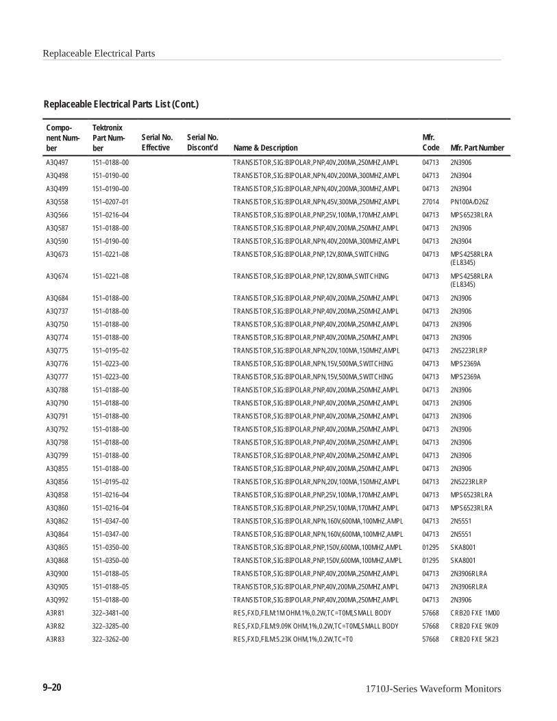
Replaceable Electrical Parts
9–20 1710J-Series Waveform Monitors
Replaceable Electrical Parts List (Cont.)
Compo-nent Num-ber Mfr. Part Number
Mfr.CodeName & Description
Serial No.Discont’d
Serial No.Effective
TektronixPart Num-ber
A3Q497 151–0188–00 TRANSISTOR,SIG:BIPOLAR,PNP,40V,200MA,250MHZ,AMPL 04713 2N3906
A3Q498 151–0190–00 TRANSISTOR,SIG:BIPOLAR,NPN,40V,200MA,300MHZ,AMPL 04713 2N3904
A3Q499 151–0190–00 TRANSISTOR,SIG:BIPOLAR,NPN,40V,200MA,300MHZ,AMPL 04713 2N3904
A3Q558 151–0207–01 TRANSISTOR,SIG:BIPOLAR,NPN,45V,300MA,250MHZ,AMPL 27014 PN100A/D26Z
A3Q566 151–0216–04 TRANSISTOR,SIG:BIPOLAR,PNP,25V,100MA,170MHZ,AMPL 04713 MPS6523RLRA
A3Q587 151–0188–00 TRANSISTOR,SIG:BIPOLAR,PNP,40V,200MA,250MHZ,AMPL 04713 2N3906
A3Q590 151–0190–00 TRANSISTOR,SIG:BIPOLAR,NPN,40V,200MA,300MHZ,AMPL 04713 2N3904
A3Q673 151–0221–08 TRANSISTOR,SIG:BIPOLAR,PNP,12V,80MA,SWITCHING 04713 MPS4258RLRA(EL8345)
A3Q674 151–0221–08 TRANSISTOR,SIG:BIPOLAR,PNP,12V,80MA,SWITCHING 04713 MPS4258RLRA(EL8345)
A3Q684 151–0188–00 TRANSISTOR,SIG:BIPOLAR,PNP,40V,200MA,250MHZ,AMPL 04713 2N3906
A3Q737 151–0188–00 TRANSISTOR,SIG:BIPOLAR,PNP,40V,200MA,250MHZ,AMPL 04713 2N3906
A3Q750 151–0188–00 TRANSISTOR,SIG:BIPOLAR,PNP,40V,200MA,250MHZ,AMPL 04713 2N3906
A3Q774 151–0188–00 TRANSISTOR,SIG:BIPOLAR,PNP,40V,200MA,250MHZ,AMPL 04713 2N3906
A3Q775 151–0195–02 TRANSISTOR,SIG:BIPOLAR,NPN,20V,100MA,150MHZ,AMPL 04713 2N5223RLRP
A3Q776 151–0223–00 TRANSISTOR,SIG:BIPOLAR,NPN,15V,500MA,SWITCHING 04713 MPS2369A
A3Q777 151–0223–00 TRANSISTOR,SIG:BIPOLAR,NPN,15V,500MA,SWITCHING 04713 MPS2369A
A3Q788 151–0188–00 TRANSISTOR,SIG:BIPOLAR,PNP,40V,200MA,250MHZ,AMPL 04713 2N3906
A3Q790 151–0188–00 TRANSISTOR,SIG:BIPOLAR,PNP,40V,200MA,250MHZ,AMPL 04713 2N3906
A3Q791 151–0188–00 TRANSISTOR,SIG:BIPOLAR,PNP,40V,200MA,250MHZ,AMPL 04713 2N3906
A3Q792 151–0188–00 TRANSISTOR,SIG:BIPOLAR,PNP,40V,200MA,250MHZ,AMPL 04713 2N3906
A3Q798 151–0188–00 TRANSISTOR,SIG:BIPOLAR,PNP,40V,200MA,250MHZ,AMPL 04713 2N3906
A3Q799 151–0188–00 TRANSISTOR,SIG:BIPOLAR,PNP,40V,200MA,250MHZ,AMPL 04713 2N3906
A3Q855 151–0188–00 TRANSISTOR,SIG:BIPOLAR,PNP,40V,200MA,250MHZ,AMPL 04713 2N3906
A3Q856 151–0195–02 TRANSISTOR,SIG:BIPOLAR,NPN,20V,100MA,150MHZ,AMPL 04713 2N5223RLRP
A3Q858 151–0216–04 TRANSISTOR,SIG:BIPOLAR,PNP,25V,100MA,170MHZ,AMPL 04713 MPS6523RLRA
A3Q860 151–0216–04 TRANSISTOR,SIG:BIPOLAR,PNP,25V,100MA,170MHZ,AMPL 04713 MPS6523RLRA
A3Q862 151–0347–00 TRANSISTOR,SIG:BIPOLAR,NPN,160V,600MA,100MHZ,AMPL 04713 2N5551
A3Q864 151–0347–00 TRANSISTOR,SIG:BIPOLAR,NPN,160V,600MA,100MHZ,AMPL 04713 2N5551
A3Q865 151–0350–00 TRANSISTOR,SIG:BIPOLAR,PNP,150V,600MA,100MHZ,AMPL 01295 SKA8001
A3Q868 151–0350–00 TRANSISTOR,SIG:BIPOLAR,PNP,150V,600MA,100MHZ,AMPL 01295 SKA8001
A3Q900 151–0188–05 TRANSISTOR,SIG:BIPOLAR,PNP,40V,200MA,250MHZ,AMPL 04713 2N3906RLRA
A3Q905 151–0188–05 TRANSISTOR,SIG:BIPOLAR,PNP,40V,200MA,250MHZ,AMPL 04713 2N3906RLRA
A3Q992 151–0188–00 TRANSISTOR,SIG:BIPOLAR,PNP,40V,200MA,250MHZ,AMPL 04713 2N3906
A3R81 322–3481–00 RES,FXD,FILM:1M OHM.1%,0.2W,TC=T0MI,SMALL BODY 57668 CRB20 FXE 1M00
A3R82 322–3285–00 RES,FXD,FILM:9.09K OHM,1%,0.2W,TC=T0MI,SMALL BODY 57668 CRB20 FXE 9K09
A3R83 322–3262–00 RES,FXD,FILM:5.23K OHM,1%,0.2W,TC=T0 57668 CRB20 FXE 5K23

Replaceable Electrical Parts
1710J-Series Waveform Monitors 9–21
Replaceable Electrical Parts List (Cont.)
Compo-nent Num-ber Mfr. Part Number
Mfr.CodeName & Description
Serial No.Discont’d
Serial No.Effective
TektronixPart Num-ber
A3R84 322–3105–00 RES,FXD:METAL FILM,121 OHM,1%,0.2W,TC=100 PPM,AXIAL 57668 CRB20 FXE 121E
A3R85 322–3414–00 RES,FXD:METAL FILM,200K OHM,1%,0.2W,TC=100 PPM,AXIAL 57668 CRB 20 FXE 200 KOHM
A3R86 322–3105–00 RES,FXD:METAL FILM,121 OHM,1%,0.2W,TC=100 PPM,AXIAL 57668 CRB20 FXE 121E
A3R98 322–3269–02 RES,FXD,FILM:6.19K OHM,0.2W,5%,TAPED & REELED 57668 CRB DYE 6K19
A3R99 322–3175–00 RES,FXD,FILM:649 OHM,1%,0.2W,TC=T0 57668 CRB20 FXE 649E
A3R001 322–3289–00 RES,FXD:METAL FILM,10K OHM,1%,0.2W,TC=100 PPM,AXIAL 91637 CCF50G10001F
A3R002 322–3269–02 RES,FXD,FILM:6.19K OHM,0.2W,5%,TAPED & REELED 57668 CRB DYE 6K19
A3R003 311–2238–00 RES,VAR,TRMR:CERMET,50K OHM,20%,0.5W,0.197 SQ TK2073 GF06UT2 503 ML20
A3R004 322–3097–00 RES,FXD:METAL FILM,100 OHM,1%,0.2W,TC=100 PPM,AXIAL 91637 CCF501G100R0F
A3R005 322–3097–00 RES,FXD:METAL FILM,100 OHM,1%,0.2W,TC=100 PPM,AXIAL 91637 CCF501G100R0F
A3R006 322–3097–00 RES,FXD:METAL FILM,100 OHM,1%,0.2W,TC=100 PPM,AXIAL 91637 CCF501G100R0F
A3R007 322–3205–00 RES,FXD,FILM:1.33K OHM,1%,0.2W,TC=T0 57668 CRB20 FXE 1K33
A3R008 322–3126–00 RES,FXD,FILM:200 OHM,1%,0.2W,TC=T0 MI,SMALL BODY 91637 CCF501G200ROF
A3R009 322–3205–00 RES,FXD,FILM:1.33K OHM,1%,0.2W,TC=T0 57668 CRB20 FXE 1K33
A3R010 322–3126–00 RES,FXD,FILM:200 OHM,1%,0.2W,TC=T0 MI,SMALL BODY 91637 CCF501G200ROF
A3R011 322–3205–00 RES,FXD,FILM:1.33K OHM,1%,0.2W,TC=T0 57668 CRB20 FXE 1K33
A3R012 322–3402–00 RES,FXD:METAL FILM,150K OHM,1%,0.2W,TC=100 PPM,AXIAL 91637 CCF50G15002F
A3R013 322–3126–00 RES,FXD,FILM:200 OHM,1%,0.2W,TC=T0 MI,SMALL BODY 91637 CCF501G200ROF
A3R014 322–3402–00 RES,FXD:METAL FILM,150K OHM,1%,0.2W,TC=100 PPM,AXIAL 91637 CCF50G15002F
A3R015 322–3402–00 RES,FXD:METAL FILM,150K OHM,1%,0.2W,TC=100 PPM,AXIAL 91637 CCF50G15002F
A3R020 322–3097–00 RES,FXD:METAL FILM,100 OHM,1%,0.2W,TC=100 PPM,AXIAL 91637 CCF501G100R0F
A3R021 322–3097–00 RES,FXD:METAL FILM,100 OHM,1%,0.2W,TC=100 PPM,AXIAL 91637 CCF501G100R0F
A3R136 322–3097–00 RES,FXD:METAL FILM,100 OHM,1%,0.2W,TC=100 PPM,AXIAL 91637 CCF501G100R0F
A3R137 322–3097–00 RES,FXD:METAL FILM,100 OHM,1%,0.2W,TC=100 PPM,AXIAL 91637 CCF501G100R0F
A3R138 322–3369–00 RES,FXD:METAL FILM,68.1K OHM,1%,0.2W,TC=100 PPM,AXIAL 57668 CRB20 FXE 68R1
A3R140 308–0297–00 RES,FXD,WW:24.7 OHM,1%,3W AXIAL LEADS,MI 05347 MS3–24R0F
A3R141 308–0297–00 RES,FXD,WW:24.7 OHM,1%,3W AXIAL LEADS,MI 05347 MS3–24R0F
A3R143 301–0101–00 RES,FXD,FILM:100 OHM,5%,0.5W MI 19701 5053CX100RDJ
A3R157 307–0023–00 RES,FXD,CMPSN:4.7 OHM,10%,0.5W MI 50139 EB47G1
A3R161 322–3289–00 RES,FXD:METAL FILM,10K OHM,1%,0.2W,TC=100 PPM,AXIAL 91637 CCF50G10001F
A3R162 322–3385–00 RES,FXD:METAL FILM,100K OHM,1%,0.2W,TC=100 PPM,AXIAL 91637 CCF501G10002F
A3R163 322–3385–00 RES,FXD:METAL FILM,100K OHM,1%,0.2W,TC=100 PPM,AXIAL 91637 CCF501G10002F
A3R164 322–3322–00 RES,FXD:METAL FILM,22.1K OHM,1%,0.2W,TC=100 PPM,AXIAL 57668 CRB20 FXE 22K1
A3R166 322–3354–00 RES,FXD:METAL FILM,47.5K OHM,1%,0.2W,TC=100 PPM,AXIAL 91637 CCF501G47501F
A3R167 311–2230–00 RES,VAR,TRMR:CERMET,500 OHM,20%,0.5W,0.197 SQ TK2073 GF06UT2 501 ML20

Replaceable Electrical Parts
9–22 1710J-Series Waveform Monitors
Replaceable Electrical Parts List (Cont.)
Compo-nent Num-ber Mfr. Part Number
Mfr.CodeName & Description
Serial No.Discont’d
Serial No.Effective
TektronixPart Num-ber
A3R168 311–2230–00 RES,VAR,TRMR:CERMET,500 OHM,20%,0.5W,0.197 SQ TK2073 GF06UT2 501 ML20
A3R180 322–3034–00 RES,FXD:METAL FILM,22.1 OHM,1%,0.2W,TC=100 PPM,AXIAL 91637 CCF50–2–G22R10FT
A3R183 301–0472–00 RES,FXD,FILM:4.7K OHM,5%,0.5W MI 19701 5053CX4K700J
A3R184 308–0783–00 RES,FXD,WW:1K OHM,1%,3W,TC=30PPM 54294 LA461ND9–1000OHM +–1PERCENT
A3R186 308–0783–00 RES,FXD,WW:1K OHM,1%,3W,TC=30PPM 54294 LA461ND9–1000OHM +–1PERCENT
A3R187 301–0472–00 RES,FXD,FILM:4.7K OHM,5%,0.5W MI 19701 5053CX4K700J
A3R189 322–3034–00 RES,FXD:METAL FILM,22.1 OHM,1%,0.2W,TC=100 PPM,AXIAL 91637 CCF50–2–G22R10FT
A3R192 322–3066–00 RES,FXD:METAL FILM,47.5 OHM,1%,0.2W,TC=100 PPM,AXIAL 09969 CCF502G47R50F
A3R196 321–0603–07 RES,FXD,FILM:15K OHM,0.1%,0.125W,TC=T9MI 07716 CEAE15001B
A3R197 322–3410–00 RES,FXD:METAL FILM,182K OHM,1%,0.2W,TC=100 PPM,AXIAL 91637 CCF501G1823FT
A3R198 321–0603–07 RES,FXD,FILM:15K OHM,0.1%,0.125W,TC=T9MI 07716 CEAE15001B
A3R199 322–3185–00 RES,FXD:METAL FILM,825 OHM,1%,0.2W,TC=100 PPM,AXIAL 57668 CRB20 FXE 825E
A3R221 322–3289–00 RES,FXD:METAL FILM,10K OHM,1%,0.2W,TC=100 PPM,AXIAL 91637 CCF50G10001F
A3R241 322–3381–00 RES,FXD,FILM:90.9K OHM,1%,0.2W,TC=T0MI,SMALL BODY 91637 CCF50–2–G9092FT
A3R242 322–3193–00 RES,FXD:METAL FILM,1K OHM,1%,0.2W,TC=100 PPM,AXIAL 91637 CCF501G10000F
A3R243 322–3318–00 RES,FXD,FILM:METAL FILM,20K OHM,1%,0.2W,TC=100 PPM 91637 CCF501G20001F
A3R246 322–3066–00 RES,FXD:METAL FILM,47.5 OHM,1%,0.2W,TC=100 PPM,AXIAL 09969 CCF502G47R50F
A3R249 322–3218–00 RES,FXD:METAL FILM,1.82K OHM,1%,0.2W,TC=100 PPM,AXIAL 57668 CRB20 FXE 1K82
A3R254 322–3254–00 RES,FXD,FILM:4.32K OHM,1%,0.2W,TC=T0MI,SMALL BODY 91637 CCF502G4321FT
A3R255 322–3193–00 RES,FXD:METAL FILM,1K OHM,1%,0.2W,TC=100 PPM,AXIAL 91637 CCF501G10000F
A3R256 322–3226–00 RES,FXD:METAL FILM,2.21K OHM,1%,0.2W,TC=100 PPM,AXIAL 91637 CCF501G22100F
A3R258 322–3289–00 RES,FXD:METAL FILM,10K OHM,1%,0.2W,TC=100 PPM,AXIAL 91637 CCF50G10001F
A3R263 322–3193–00 RES,FXD:METAL FILM,1K OHM,1%,0.2W,TC=100 PPM,AXIAL 91637 CCF501G10000F
A3R264 322–3172–00 RES,FXD,FILM:604 OHM,1%,0.2W,TC=T0MI,SMALL BODY 57668 CRB20 FXE 604E
A3R266 322–3258–00 RES,FXD:METAL FILM,4.75K OHM,1%,0.2W,TC=100 PPM,AXIAL 56845 CCF50–2–G4751FT
A3R267 322–3258–00 RES,FXD:METAL FILM,4.75K OHM,1%,0.2W,TC=100 PPM,AXIAL 56845 CCF50–2–G4751FT
A3R268 322–3172–00 RES,FXD,FILM:604 OHM,1%,0.2W,TC=T0MI,SMALL BODY 57668 CRB20 FXE 604E
A3R272 322–3289–00 RES,FXD:METAL FILM,10K OHM,1%,0.2W,TC=100 PPM,AXIAL 91637 CCF50G10001F
A3R273 322–3363–00 RES,FXD,FILM:59K OHM,1%,0.2W,TC=T0MI,SMALL BODY 57668 CRB20 FXE 59K0
A3R274 311–2240–00 RES,VAR,NONWW:TRMR,200K OHM,20%,0.5W LINEAR TK2073 GF06UT2 204 ML20
A3R276 322–3097–00 RES,FXD:METAL FILM,100 OHM,1%,0.2W,TC=100 PPM,AXIAL 91637 CCF501G100R0F
A3R294 322–3210–00 RES,FXD:METAL FILM,1.5K OHM,1%,0.2W,TC=100 PPM,AXIAL 57668 CRB20 FXE 1K50
A3R295 315–0220–00 RES,FXD,FILM:22 OHM,5%,0.25W MI 50139 CB2205
A3R296 322–3097–00 RES,FXD:METAL FILM,100 OHM,1%,0.2W,TC=100 PPM,AXIAL 91637 CCF501G100R0F
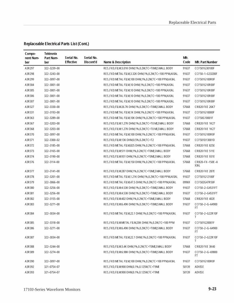
Replaceable Electrical Parts
1710J-Series Waveform Monitors 9–23
Replaceable Electrical Parts List (Cont.)
Compo-nent Num-ber Mfr. Part Number
Mfr.CodeName & Description
Serial No.Discont’d
Serial No.Effective
TektronixPart Num-ber
A3R297 322–3239–00 RES,FXD,FILM:3.01K OHM,1%,0.2W,TC=T0MI,SMALL BODY 91637 CCF501G30100F
A3R298 322–3243–00 RES,FXD:METAL FILM,3.32K OHM,1%,0.2W,TC=100 PPM,AXIAL 91637 CCF50–1–G33200F
A3R299 322–3097–00 RES,FXD:METAL FILM,100 OHM,1%,0.2W,TC=100 PPM,AXIAL 91637 CCF501G100R0F
A3R304 322–3001–00 RES,FXD:METAL FILM,10 OHM,1%,0.2W,TC=100 PPM,AXIAL 91637 CCF501G10R00F
A3R305 322–3001–00 RES,FXD:METAL FILM,10 OHM,1%,0.2W,TC=100 PPM,AXIAL 91637 CCF501G10R00F
A3R306 322–3001–00 RES,FXD:METAL FILM,10 OHM,1%,0.2W,TC=100 PPM,AXIAL 91637 CCF501G10R00F
A3R307 322–3001–00 RES,FXD:METAL FILM,10 OHM,1%,0.2W,TC=100 PPM,AXIAL 91637 CCF501G10R00F
A3R327 322–3330–00 RES,FXD,FILM:26.7K OHM,1%,0.2W,TC=T0MI,SMALL BODY 57668 CRB20 FXE 26K7
A3R331 322–3193–00 RES,FXD:METAL FILM,1K OHM,1%,0.2W,TC=100 PPM,AXIAL 91637 CCF501G10000F
A3R363 322–3289–00 RES,FXD:METAL FILM,10K OHM,1%,0.2W,TC=100 PPM,AXIAL 91637 CCF50G10001F
A3R367 322–3203–00 RES,FXD,FILM:1.27K OHM,1%,0.2W,TC=T0 MI,SMALL BODY 57668 CRB20 FXE 1K27
A3R368 322–3203–00 RES,FXD,FILM:1.27K OHM,1%,0.2W,TC=T0 MI,SMALL BODY 57668 CRB20 FXE 1K27
A3R370 322–3097–00 RES,FXD:METAL FILM,100 OHM,1%,0.2W,TC=100 PPM,AXIAL 91637 CCF501G100R0F
A3R371 322–3300–02 RES,FXD,FILM:13K OHM,0.5%,0.2W,TC=T2 91637 CCF501D13001D
A3R372 322–3185–00 RES,FXD:METAL FILM,825 OHM,1%,0.2W,TC=100 PPM,AXIAL 57668 CRB20 FXE 825E
A3R373 322–3165–00 RES,FXD,FILM:511 OHM,1%,0.2W,TC=T0MI,SMALL BODY 57668 CRB20 FXE 511E
A3R374 322–3190–00 RES,FXD,FILM:931 OHM,1%,0.2W,TC=T0MI,SMALL BODY 57668 CRB20 FXE 931E
A3R376 322–3114–00 RES,FXD:METAL FILM,150 OHM,1%,0.2W,TC=100 PPM,AXIAL 57668 CRB20–FX–150E–AXIAL
A3R377 322–3141–00 RES,FXD,FILM:287 OHM,1%,0.2W,TC=T0MI,SMALL BODY 57668 CRB20 FXE 287E
A3R378 322–3201–00 RES,FXD:METAL FILM,1.21K OHM,1%,0.2W,TC=100 PPM,AXIAL 91637 CCF501G12100F
A3R379 322–3066–00 RES,FXD:METAL FILM,47.5 OHM,1%,0.2W,TC=100 PPM,AXIAL 09969 CCF502G47R50F
A3R380 322–3256–00 RES,FXD,FILM:4.53K OHM,1%,0.2W,TC=T0MI,SMALL BODY 91637 CCF50–2–G4531FT
A3R381 322–3256–00 RES,FXD,FILM:4.53K OHM,1%,0.2W,TC=T0MI,SMALL BODY 91637 CCF50–2–G4531FT
A3R382 322–3155–00 RES,FXD,FILM:402 OHM,1%,0.2W,TC=T0MI,SMALL BODY 57668 CRB20 FXE 402E
A3R383 322–3271–00 RES,FXD,FILM:6.49K OHM,1%,0.2W,TC=T0MI,SMALL BODY 91637 CCF50–2–G–64900FT
A3R384 322–3034–00 RES,FXD:METAL FILM,22.1 OHM,1%,0.2W,TC=100 PPM,AXIAL 91637 CCF50–2–G22R10FT
A3R385 322–3318–00 RES,FXD,FILM:METAL FILM,20K OHM,1%,0.2W,TC=100 PPM 91637 CCF501G20001F
A3R386 322–3271–00 RES,FXD,FILM:6.49K OHM,1%,0.2W,TC=T0MI,SMALL BODY 91637 CCF50–2–G–64900FT
A3R387 322–3034–00 RES,FXD:METAL FILM,22.1 OHM,1%,0.2W,TC=100 PPM,AXIAL 91637 CCF50–2–G22R10FT
A3R388 322–3244–00 RES,FXD,FILM:3.4K OHM,1%,0.2W,TC=T0MI,SMALL BODY 57668 CRB20 FXE 3K40
A3R389 322–3274–00 RES,FXD,FILM:6.98K OHM,1%,0.2W,TC=T0MI,SMALL BODY 91637 CCF50–2–G–69800FT
A3R390 322–3097–00 RES,FXD:METAL FILM,100 OHM,1%,0.2W,TC=100 PPM,AXIAL 91637 CCF501G100R0F
A3R392 321–0754–07 RES,FXD,FILM:900 OHM,0.1%,0.125W,TC=T9MI 50139 ADVISE
A3R393 321–0754–07 RES,FXD,FILM:900 OHM,0.1%,0.125W,TC=T9MI 50139 ADVISE

Replaceable Electrical Parts
9–24 1710J-Series Waveform Monitors
Replaceable Electrical Parts List (Cont.)
Compo-nent Num-ber Mfr. Part Number
Mfr.CodeName & Description
Serial No.Discont’d
Serial No.Effective
TektronixPart Num-ber
A3R394 322–3147–00 RES,FXD:METAL FILM,332 OHM,1%,0.2W,TC=100 PPM,AXIAL 57668 CRB20 FXE 332E
A3R395 322–3289–00 RES,FXD:METAL FILM,10K OHM,1%,0.2W,TC=100 PPM 91637 CCF50G10001F
A3R409 322–3001–00 672–1333–13 RES,FXD:METAL FILM,10 OHM,1%,0.2W,TC=100 PPM,AXIAL 91637 CCF501G10R00F
A3R409 131–4566–00 672–1333–14 BUS,CONDUCTOR:0 OHM,300 SPACING,SM BODY MI,DUMMY 91637 FRJ–50
A3R409 322–3001–00 672–1465–03 RES,FXD:METAL FILM,10 OHM,1%,0.2W,TC=100 PPM,AXIAL 91637 CCF501G10R00F
A3R409 322–3001–00 672–1465–04 BUS,CONDUCTOR:0 OHM,300 SPACING,SM BODY MI,DUMMY 91637 FRJ–50
A3R441 322–3258–00 RES,FXD:METAL FILM,4.75K OHM,1%,0.2W,TC=100 PPM,AXIAL 56845 CCF50–2–G4751FT
A3R442 322–3258–00 RES,FXD:METAL FILM,4.75K OHM,1%,0.2W,TC=100 PPM,AXIAL 56845 CCF50–2–G4751FT
A3R444 322–3356–00 RES,FXD,FILM:49.9K OHM,1%,0.2W,TC=T0MI,SMALL BODY 57668 CRB20 FXE 49K9
A3R445 322–3356–00 RES,FXD,FILM:49.9K OHM,1%,0.2W,TC=T0MI,SMALL BODY 57668 CRB20 FXE 49K9
A3R446 322–3289–00 RES,FXD:METAL FILM,10K OHM,1%,0.2W,TC=100 PPM,AXIAL 91637 CCF50G10001F
A3R447 322–3289–00 RES,FXD:METAL FILM,10K OHM,1%,0.2W,TC=100 PPM,AXIAL 91637 CCF50G10001F
A3R448 322–3318–00 RES,FXD,FILM:METAL FILM,20K OHM,1%,0.2W,TC=100 PPM 91637 CCF501G20001F
A3R449 322–3410–00 RES,FXD:METAL FILM,182K OHM,1%,0.2W,TC=100 PPM,AXIAL 91637 CCF501G1823FT
A3R454 322–3231–00 RES,FXD,FILM:2.49K OHM,1%,0.2W,TC=T0MI,SMALL BODY 57668 CRB20 FXE 2K49
A3R455 322–3231–00 RES,FXD,FILM:2.49K OHM,1%,0.2W,TC=T0MI,SMALL BODY 57668 CRB20 FXE 2K49
A3R456 322–3117–00 RES,FXD,FILM:162 OHM,1%,0.2W,TC=T0MI,SMALL BODY 57668 CRB 20 FXE 162E
A3R457 322–3097–00 RES,FXD:METAL FILM,100 OHM,1%,0.2W,TC=100 PPM,AXIAL 91637 CCF501G100R0F
A3R459 322–3295–00 RES,FXD:METAL FILM,11.5K OHM,1%,0.2W,TC=100 PPM,AXIAL 57668 CRB20 FXE 11K5
A3R460 322–3481–00 RES,FXD,FILM:1M OHM.1%,0.2W,TC=T0MI,SMALL BODY 57668 CRB20 FXE 1M00
A3R463 322–3295–00 RES,FXD:METAL FILM,11.5K OHM,1%,0.2W,TC=100 PPM,AXIAL 57668 CRB20 FXE 11K5
A3R465 322–3243–00 RES,FXD:METAL FILM,3.32K OHM,1%,0.2W,TC=100 PPM,AXIAL 91637 CCF50–1–G33200F
A3R466 322–3258–00 RES,FXD:METAL FILM,4.75K OHM,1%,0.2W,TC=100 PPM,AXIAL 56845 CCF50–2–G4751FT
A3R470 322–3114–00 RES,FXD:METAL FILM,150 OHM,1%,0.2W,TC=100 PPM,AXIAL 57668 CRB20–FX–150E–AXIAL
A3R471 322–3289–00 RES,FXD:METAL FILM,10K OHM,1%,0.2W,TC=100 PPM,AXIAL 91637 CCF50G10001F
A3R472 322–3210–00 RES,FXD:METAL FILM,1.5K OHM,1%,0.2W,TC=100 PPM,AXIAL 57668 CRB20 FXE 1K50
A3R473 322–3226–00 RES,FXD:METAL FILM,2.21K OHM,1%,0.2W,TC=100 PPM,AXIAL 91637 CCF501G22100F
A3R474 322–3147–00 RES,FXD:METAL FILM,332 OHM,1%,0.2W,TC=100 PPM,AXIAL 57668 CRB20 FXE 332E
A3R475 322–3222–00 RES,FXD:METAL FILM,2K OHM,1%,0.2W,TC=100 PPM,AXIAL 91637 CCF501G20000F
A3R477 322–3311–00 RES,FXD,FILM:16.9K OHM,1%,0.2W,TC=T0MI,SMALL BODY 56845 CCF–50–2–1692F
A3R478 322–3193–00 RES,FXD:METAL FILM,1K OHM,1%,0.2W,TC=100 PPM,AXIAL 91637 CCF501G10000F
A3R479 322–3243–00 RES,FXD:METAL FILM,3.32K OHM,1%,0.2W,TC=100 PPM,AXIAL 91637 CCF50–1–G33200F
A3R480 322–3235–00 RES,FXD:METAL FILM,2.74K OHM,1%,0.2W,TC=100 PPM,AXIAL 57668 CRB20 FXE 2K74
A3R481 322–3001–00 RES,FXD:METAL FILM,10 OHM,1%,0.2W,TC=100 PPM,AXIAL 91637 CCF501G10R00F
A3R482 322–3156–00 RES,FXD,FILM:412 OHM,1%,0.2W,TC=T0MI,SMALL BODY 57668 CRB20 FXE 412E
A3R483 322–3156–00 RES,FXD,FILM:412 OHM,1%,0.2W,TC=T0MI,SMALL BODY 57668 CRB20 FXE 412E
A3R484 322–3322–00 RES,FXD:METAL FILM,22.1K OHM,1%,0.2W,TC=100 PPM,AXIAL 57668 CRB20 FXE 22K1

Replaceable Electrical Parts
1710J-Series Waveform Monitors 9–25
Replaceable Electrical Parts List (Cont.)
Compo-nent Num-ber Mfr. Part Number
Mfr.CodeName & Description
Serial No.Discont’d
Serial No.Effective
TektronixPart Num-ber
A3R485 322–3062–00 RES,FXD,FILM:43.2 OHM,1%,0.2W,TC=T0MI,SMALL BODY 57668 RB20FXE43E2
A3R486 322–3083–00 RES,FXD,FILM:71.5 OHM,1%,0.2W,TC=T0MI,SMALL BODY 57668 CRB20 FXE 71E5
A3R487 322–3222–00 RES,FXD:METAL FILM,2K OHM,1%,0.2W,TC=100 PPM,AXIAL 91637 CCF501G20000F
A3R489 311–2230–00 RES,VAR,TRMR:CERMET,500 OHM,20%,0.5W,0.197 SQ TK2073 GF06UT2 501 ML20
A3R491 322–3410–00 RES,FXD:METAL FILM,182K OHM,1%,0.2W,TC=100 PPM,AXIAL 91637 CCF501G1823FT
A3R492 311–0614–00 RES,VAR,NONWW:TRMR,30K OHM,0.5W CERMET 32997 3329H–L58–303
A3R493 322–3097–00 RES,FXD:METAL FILM,100 OHM,1%,0.2W,TC=100 PPM,AXIAL 91637 CCF501G100R0F
A3R495 322–3289–00 RES,FXD:METAL FILM,10K OHM,1%,0.2W,TC=100 PPM,AXIAL 91637 CCF50G10001F
A3R497 322–3147–00 RES,FXD:METAL FILM,332 OHM,1%,0.2W,TC=100 PPM,AXIAL 57668 CRB20 FXE 332E
A3R498 322–3097–00 RES,FXD:METAL FILM,100 OHM,1%,0.2W,TC=100 PPM,AXIAL 91637 CCF501G100R0F
A3R499 322–3243–00 RES,FXD:METAL FILM,3.32K OHM,1%,0.2W,TC=100 PPM,AXIAL 91637 CCF50–1–G33200F
A3R504 322–3193–00 RES,FXD:METAL FILM,1K OHM,1%,0.2W,TC=100 PPM,AXIAL 91637 CCF501G10000F
A3R505 322–3193–00 RES,FXD:METAL FILM,1K OHM,1%,0.2W,TC=100 PPM,AXIAL 91637 CCF501G10000F
A3R506 322–3193–00 RES,FXD:METAL FILM,1K OHM,1%,0.2W,TC=100 PPM,AXIAL 91637 CCF501G10000F
A3R507 322–3193–00 RES,FXD:METAL FILM,1K OHM,1%,0.2W,TC=100 PPM,AXIAL 91637 CCF501G10000F
A3R526 322–3289–00 RES,FXD:METAL FILM,10K OHM,1%,0.2W,TC=100 PPM,AXIAL 91637 CCF50G10001F
A3R538 322–3289–00 RES,FXD:METAL FILM,10K OHM,1%,0.2W,TC=100 PPM,AXIAL 91637 CCF50G10001F
A3R544 322–3246–00 RES,FXD,FILM:3.57K OHM,1%,0.2W,TC=T0MI,SMALL BODY 57668 CRB20 FXE 3K57
A3R545 322–3277–00 RES,FXD,FILM:7.5K OHM,1%,0.2W,TC=T0 57668 CRB20 FXE 7K50
A3R546 322–3162–00 RES,FXD:METAL FILM,475 OHM,1%,0.2W,TC=100 PPM,AXIAL 91637 CCF50G475R0F
A3R547 322–3258–00 RES,FXD:METAL FILM,4.75K OHM,1%,0.2W,TC=100 PPM,AXIAL 56845 CCF50–2–G4751FT
A3R548 322–3339–00 RES,FXD:METAL FILM,33.2K OHM,1%,0.2W,TC=100 PPM,AXIAL 91637 CCF50–2–G3322FT
A3R549 322–3354–00 RES,FXD:METAL FILM,47.5K OHM,1%,0.2W,TC=100 PPM,AXIAL 91637 CCF501G47501F
A3R550 322–3034–00 RES,FXD:METAL FILM,22.1 OHM,1%,0.2W,TC=100 PPM,AXIAL 91637 CCF50–2–G22R10FT
A3R551 322–3329–00 RES,FXD,FILM:26.1K OHM.1%,0.2W,TC=T0MI,SMALL BODY 57668 CRB20 FXE 26K1
A3R552 311–2227–00 RES,VAR,TRMR:CERMET,100 OHM,20%,0.5W,0.197 SQ 30983 ORDER BY DESCR
A3R553 311–2227–00 RES,VAR,TRMR:CERMET,100 OHM,20%,0.5W,0.197 SQ 30983 ORDER BY DESCR
A3R554 322–3089–00 RES,FXD:METAL FILM,82.5 OHM,1%.0.2W,TC=100 PPM,AXIAL 57668 CRB20 FXE 82E5
A3R555 322–3030–00 RES,FXD:METAL FILM,20 OHM,1%,0.2W,TC=100 PPM,AXIAL 57668 CRB 20 FXE 20E0
A3R556 322–3295–00 RES,FXD:METAL FILM,11.5K OHM,1%,0.2W,TC=100 PPM,AXIAL 57668 CRB20 FXE 11K5
A3R557 322–3232–00 RES,FXD,FILM:2.55K OHM,1%,0.2W,TC=T0 MI,SMALL BODY 57668 CRB20 FXE 2K55
A3R558 322–3232–00 RES,FXD,FILM:2.55K OHM,1%,0.2W,TC=T0 MI,SMALL BODY 57668 CRB20 FXE 2K55
A3R559 322–3200–00 RES,FXD,FILM:1.18K OHM,1%,0.2W,TC=T0 MI,SMALL BODY 91637 CCF501G11800F
A3R563 322–3226–00 RES,FXD:METAL FILM,2.21K OHM,1%,0.2W,TC=100 PPM,AXIAL 91637 CCF501G22100F
A3R564 322–3097–00 RES,FXD:METAL FILM,100 OHM,1%,0.2W,TC=100 PPM,AXIAL 91637 CCF501G100R0F
A3R565 322–3289–00 RES,FXD:METAL FILM,10K OHM,1%,0.2W,TC=100 PPM,AXIAL 91637 CCF50G10001F
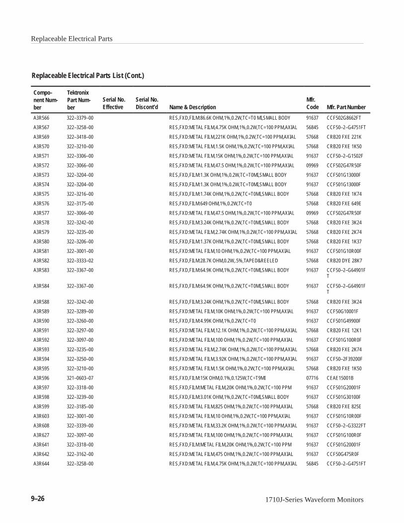
Replaceable Electrical Parts
9–26 1710J-Series Waveform Monitors
Replaceable Electrical Parts List (Cont.)
Compo-nent Num-ber Mfr. Part Number
Mfr.CodeName & Description
Serial No.Discont’d
Serial No.Effective
TektronixPart Num-ber
A3R566 322–3379–00 RES,FXD,FILM:86.6K OHM,1%,0.2W,TC=T0 MI,SMALL BODY 91637 CCF502G8662FT
A3R567 322–3258–00 RES,FXD:METAL FILM,4.75K OHM,1%,0.2W,TC=100 PPM,AXIAL 56845 CCF50–2–G4751FT
A3R569 322–3418–00 RES,FXD:METAL FILM,221K OHM,1%,0.2W,TC=100 PPM,AXIAL 57668 CRB20 FXE 221K
A3R570 322–3210–00 RES,FXD:METAL FILM,1.5K OHM,1%,0.2W,TC=100 PPM,AXIAL 57668 CRB20 FXE 1K50
A3R571 322–3306–00 RES,FXD:METAL FILM,15K OHM,1%,0.2W,TC=100 PPM,AXIAL 91637 CCF50–2–G1502F
A3R572 322–3066–00 RES,FXD:METAL FILM,47.5 OHM,1%,0.2W,TC=100 PPM,AXIAL 09969 CCF502G47R50F
A3R573 322–3204–00 RES,FXD,FILM:1.3K OHM,1%,0.2W,TC=T0MI,SMALL BODY 91637 CCF501G13000F
A3R574 322–3204–00 RES,FXD,FILM:1.3K OHM,1%,0.2W,TC=T0MI,SMALL BODY 91637 CCF501G13000F
A3R575 322–3216–00 RES,FXD,FILM:1.74K OHM,1%,0.2W,TC=T0MI,SMALL BODY 57668 CRB20 FXE 1K74
A3R576 322–3175–00 RES,FXD,FILM:649 OHM,1%,0.2W,TC=T0 57668 CRB20 FXE 649E
A3R577 322–3066–00 RES,FXD:METAL FILM,47.5 OHM,1%,0.2W,TC=100 PPM,AXIAL 09969 CCF502G47R50F
A3R578 322–3242–00 RES,FXD,FILM:3.24K OHM,1%,0.2W,TC=T0MI,SMALL BODY 57668 CRB20 FXE 3K24
A3R579 322–3235–00 RES,FXD:METAL FILM,2.74K OHM,1%,0.2W,TC=100 PPM,AXIAL 57668 CRB20 FXE 2K74
A3R580 322–3206–00 RES,FXD,FILM:1.37K OHM,1%,0.2W,TC=T0MI,SMALL BODY 57668 CRB20 FXE 1K37
A3R581 322–3001–00 RES,FXD:METAL FILM,10 OHM,1%,0.2W,TC=100 PPM,AXIAL 91637 CCF501G10R00F
A3R582 322–3333–02 RES,FXD,FILM:28.7K OHM,0.2W,.5%,TAPED&REELED 57668 CRB20 DYE 28K7
A3R583 322–3367–00 RES,FXD,FILM:64.9K OHM,1%,0.2W,TC=T0MI,SMALL BODY 91637 CCF50–2–G64901FT
A3R584 322–3367–00 RES,FXD,FILM:64.9K OHM,1%,0.2W,TC=T0MI,SMALL BODY 91637 CCF50–2–G64901FT
A3R588 322–3242–00 RES,FXD,FILM:3.24K OHM,1%,0.2W,TC=T0MI,SMALL BODY 57668 CRB20 FXE 3K24
A3R589 322–3289–00 RES,FXD:METAL FILM,10K OHM,1%,0.2W,TC=100 PPM,AXIAL 91637 CCF50G10001F
A3R590 322–3260–00 RES,FXD,FILM:4.99K OHM,1%,0.2W,TC=T0 91637 CCF501G49900F
A3R591 322–3297–00 RES,FXD:METAL FILM,12.1K OHM,1%,0.2W,TC=100 PPM,AXIAL 57668 CRB20 FXE 12K1
A3R592 322–3097–00 RES,FXD:METAL FILM,100 OHM,1%,0.2W,TC=100 PPM,AXIAL 91637 CCF501G100R0F
A3R593 322–3235–00 RES,FXD:METAL FILM,2.74K OHM,1%,0.2W,TC=100 PPM,AXIAL 57668 CRB20 FXE 2K74
A3R594 322–3250–00 RES,FXD:METAL FILM,3.92K OHM,1%,0.2W,TC=100 PPM,AXIAL 91637 CCF50–2F39200F
A3R595 322–3210–00 RES,FXD:METAL FILM,1.5K OHM,1%,0.2W,TC=100 PPM,AXIAL 57668 CRB20 FXE 1K50
A3R596 321–0603–07 RES,FXD,FILM:15K OHM,0.1%,0.125W,TC=T9MI 07716 CEAE15001B
A3R597 322–3318–00 RES,FXD,FILM:METAL FILM,20K OHM,1%,0.2W,TC=100 PPM 91637 CCF501G20001F
A3R598 322–3239–00 RES,FXD,FILM:3.01K OHM,1%,0.2W,TC=T0MI,SMALL BODY 91637 CCF501G30100F
A3R599 322–3185–00 RES,FXD:METAL FILM,825 OHM,1%,0.2W,TC=100 PPM,AXIAL 57668 CRB20 FXE 825E
A3R603 322–3001–00 RES,FXD:METAL FILM,10 OHM,1%,0.2W,TC=100 PPM,AXIAL 91637 CCF501G10R00F
A3R608 322–3339–00 RES,FXD:METAL FILM,33.2K OHM,1%,0.2W,TC=100 PPM,AXIAL 91637 CCF50–2–G3322FT
A3R627 322–3097–00 RES,FXD:METAL FILM,100 OHM,1%,0.2W,TC=100 PPM,AXIAL 91637 CCF501G100R0F
A3R641 322–3318–00 RES,FXD,FILM:METAL FILM,20K OHM,1%,0.2W,TC=100 PPM 91637 CCF501G20001F
A3R642 322–3162–00 RES,FXD:METAL FILM,475 OHM,1%,0.2W,TC=100 PPM,AXIAL 91637 CCF50G475R0F
A3R644 322–3258–00 RES,FXD:METAL FILM,4.75K OHM,1%,0.2W,TC=100 PPM,AXIAL 56845 CCF50–2–G4751FT

Replaceable Electrical Parts
1710J-Series Waveform Monitors 9–27
Replaceable Electrical Parts List (Cont.)
Compo-nent Num-ber Mfr. Part Number
Mfr.CodeName & Description
Serial No.Discont’d
Serial No.Effective
TektronixPart Num-ber
A3R649 322–3356–00 RES,FXD,FILM:49.9K OHM,1%,0.2W,TC=T0MI,SMALL BODY 57668 CRB20 FXE 49K9
A3R650 322–3318–00 RES,FXD,FILM:METAL FILM,20K OHM,1%,0.2W,TC=100 PPM 91637 CCF501G20001F
A3R651 322–3322–00 RES,FXD:METAL FILM,22.1K OHM,1%,0.2W,TC=100 PPM,AXIAL 57668 CRB20 FXE 22K1
A3R652 322–3354–00 RES,FXD:METAL FILM,47.5K OHM,1%,0.2W,TC=100 PPM,AXIAL 91637 CCF501G47501F
A3R653 322–3222–00 RES,FXD:METAL FILM,2K OHM,1%,0.2W,TC=100 PPM,AXIAL 91637 CCF501G20000F
A3R654 322–3220–00 RES,FXD,FILM:1.91K OHM,1%,0.2W,TC=T0MI,SMALL BODY 57668 CRB20 FXE 1K91
A3R655 322–3310–00 RES,FXD,FILM:16.5K OHM,1%,0.2W,TC=T0 57668 CRB20 FXE 16K5
A3R656 321–0380–00 RES,FXD,FILM:88.7K OHM,1%,0.125W,TC=T0 MI 50139 NOT AVAILABLE
A3R657 322–3251–00 RES,FXD,FILM:4.02K OHM,1%,0.2W,TC=T0 91637 CCF501G40200F
A3R658 322–3200–00 RES,FXD,FILM:1.18K OHM,1%,0.2W,TC=T0 MI,SMALL BODY 91637 CCF501G11800F
A3R659 322–3066–00 RES,FXD:METAL FILM,47.5 OHM,1%,0.2W,TC=100 PPM,AXIAL 09969 CCF502G47R50F
A3R660 311–2234–00 RES,VAR,TRMR:CERMET,5K OHM,20%,0.5W,0.197 SQ TK2073 GF06UT2 502 ML20
A3R661 311–2234–00 RES,VAR,TRMR:CERMET,5K OHM,20%,0.5W,0.197 SQ TK2073 GF06UT2 502 ML20
A3R664 322–3165–00 RES,FXD,FILM:511 OHM,1%,0.2W,TC=T0MI,SMALL BODY 57668 CRB20 FXE 511E
A3R667 322–3258–00 RES,FXD:METAL FILM,4.75K OHM,1%,0.2W,TC=100 PPM,AXIAL 56845 CCF50–2–G4751FT
A3R668 322–3258–00 RES,FXD:METAL FILM,4.75K OHM,1%,0.2W,TC=100 PPM,AXIAL 56845 CCF50–2–G4751FT
A3R669 322–3377–00 RES,FXD:METAL FILM,82.5K OHM,1%,0.2W,TC=100 PPM,AXIAL 91637 CCF50–2F82501F
A3R670 322–3222–00 RES,FXD:METAL FILM,2K OHM,1%,0.2W,TC=100 PPM,AXIAL 91637 CCF501G20000F
A3R671 322–3239–00 RES,FXD,FILM:3.01K OHM,1%,0.2W,TC=T0MI,SMALL BODY 91637 CCF501G30100F
A3R672 322–3193–00 RES,FXD:METAL FILM,1K OHM,1%,0.2W,TC=100 PPM,AXIAL 91637 CCF501G10000F
A3R673 322–3258–00 RES,FXD:METAL FILM,4.75K OHM,1%,0.2W,TC=100 PPM,AXIAL 56845 CCF50–2–G4751FT
A3R674 322–3258–00 RES,FXD:METAL FILM,4.75K OHM,1%,0.2W,TC=100 PPM,AXIAL 56845 CCF50–2–G4751FT
A3R675 322–3172–00 RES,FXD,FILM:604 OHM,1%,0.2W,TC=T0MI,SMALL BODY 57668 CRB20 FXE 604E
A3R676 322–3289–00 RES,FXD:METAL FILM,10K OHM,1%,0.2W,TC=100 PPM,AXIAL 91637 CCF50G10001F
A3R677 322–3297–00 RES,FXD:METAL FILM,12.1K OHM,1%,0.2W,TC=100 PPM,AXIAL 57668 CRB20 FXE 12K1
A3R678 322–3335–00 RES,FXD,FILM:30.1K OHM,1%,0.2W,TC=T0MI,SMALL BODY 57668 CRB20 FXE 30K1
A3R679 322–3335–00 RES,FXD,FILM:30.1K OHM,1%,0.2W,TC=T0MI,SMALL BODY 57668 CRB20 FXE 30K1
A3R680 311–2232–00 RES,VAR,TRMR:CERMET,2K OHM,20%,0.5W,0.197 SQ 30983 ORDER BY DESCR
A3R681 322–3346–00 RES,FXD:METAL FILM,39.2K OHM,1%,0.2W,TC=100 PPM,AXIAL 57668 CRB20FXE39K2
A3R682 322–3179–00 RES,FXD,FILM:715 OHM,1%,0.2W,TC=T0 MI,SMALL BODY 57668 CRB20 FXE 715E
A3R683 311–2233–00 RES,VAR,TRMR:CERMET,3K OHM,20%,0.5W,0.197 SQ TK2073 GF06UT2 302 ML20
A3R687 322–3275–00 RES,FXD,FILM:7.15K OHM,1%,0.2W,TC=T0MI,SMALL BODY 57668 CRB20 FXE 7K15
A3R688 322–3268–00 RES,FXD,FILM:6.04K OHM,1%,0.2W,TC=T0MI,SMALL BODY 57668 CRB20 FXE 6K04
A3R689 311–2234–00 RES,VAR,TRMR:CERMET,5K OHM,20%,0.5W,0.197 SQ TK2073 GF06UT2 502 ML20
A3R690 322–3297–00 RES,FXD:METAL FILM,12.1K OHM,1%,0.2W,TC=100 PPM,AXIAL 57668 CRB20 FXE 12K1

Replaceable Electrical Parts
9–28 1710J-Series Waveform Monitors
Replaceable Electrical Parts List (Cont.)
Compo-nent Num-ber Mfr. Part Number
Mfr.CodeName & Description
Serial No.Discont’d
Serial No.Effective
TektronixPart Num-ber
A3R691 322–3297–00 RES,FXD:METAL FILM,12.1K OHM,1%,0.2W,TC=100 PPM,AXIAL 57668 CRB20 FXE 12K1
A3R692 322–3239–00 RES,FXD,FILM:3.01K OHM,1%,0.2W,TC=T0MI,SMALL BODY 91637 CCF501G30100F
A3R694 322–3193–00 RES,FXD:METAL FILM,1K OHM,1%,0.2W,TC=100 PPM,AXIAL 91637 CCF501G10000F
A3R695 322–3164–00 RES,FXD,FILM:499 OHM,1%,0.2W,TC=T0MI,SMALL BODY 91637 CCF501G499ROF
A3R696 321–0603–07 RES,FXD,FILM:15K OHM,0.1%,0.125W,TC=T9MI 07716 CEAE15001B
A3R697 322–3410–00 RES,FXD:METAL FILM,182K OHM,1%,0.2W,TC=100 PPM,AXIAL 91637 CCF501G1823FT
A3R698 315–0220–00 RES,FXD,FILM:22 OHM,5%,0.25W MI 50139 CB2205
A3R700 311–2269–00 RES,VAR,NONWW:TRMR,20K OHM,20%,0.5W LINEAR,MI 30983 ADVISE
A3R701 311–2269–00 RES,VAR,NONWW:TRMR,20K OHM,20%,0.5W LINEAR,MI 30983 ADVISE
A3R736 322–3289–00 RES,FXD:METAL FILM,10K OHM,1%,0.2W,TC=100 PPM,AXIAL 91637 CCF50G10001F
A3R740 322–3322–00 672–1333–12 RES,FXD:METAL FILM,22.1K OHM,1%,0.2W,TC=100 PPM,AXIAL 57668 CRB20 FXE 22K1
A3R740 322–3326–00 672–1333–13 RES,FXD,FILM:24.3K OHM,1%,0.2W,TC–T0 MI,SMALL BODY 91637 CCF50–2432F–R36
A3R740 322–3322–00 672–1465–02 RES,FXD:METAL FILM,22.1K OHM,1%,0.2W,TC=100 PPM,AXIAL 57668 CRB20 FXE 22K1
A3R740 322–3326–00 672–1465–03 RES,FXD,FILM:24.3K OHM,1%,0.2W,TC–T0 MI,SMALL BODY 91637 CCF50–2432F–R36
A3R746 322–3258–00 RES,FXD:METAL FILM,4.75K OHM,1%,0.2W,TC=100 PPM,AXIAL 56845 CCF50–2–G4751FT
A3R750 322–3412–00 RES,FXD,FILM:191K OHM,1%,0.2W,TC=T0MI,SMALL BODY 57668 CRB20 FXE 191K
A3R751 322–3354–00 RES,FXD:METAL FILM,47.5K OHM,1%,0.2W,TC=100 PPM,AXIAL 91637 CCF501G47501F
A3R752 322–3336–00 RES,FXD,FILM:30.9K OHM,1%,0.2W,TC=T0MI,SMALL BODY 91637 CCF50–2F30901F
A3R753 322–3437–00 RES,FXD,FILM:348K OHM,1%,0.2W,TC=T0 MI,SMALL BODY 57668 CRB20 FXE 348K
A3R754 322–3402–00 RES,FXD:METAL FILM,150K OHM,1%,0.2W,TC=100 PPM,AXIAL 91637 CCF50G15002F
A3R755 322–3189–00 RES,FXD,FILM:909 OHM,1%,0.2W,TC=T0MI,SMALL BODY 57668 CRB 20 FXE 909E
A3R756 322–3300–02 RES,FXD,FILM:13K OHM,0.5%,0.2W,TC=T2 91637 CCF501D13001D
A3R757 322–3311–00 RES,FXD,FILM:16.9K OHM,1%,0.2W,TC=T0MI,SMALL BODY 56845 CCF–50–2–1692F
A3R759 322–3179–00 RES,FXD,FILM:715 OHM,1%,0.2W,TC=T0 MI,SMALL BODY 57668 CRB20 FXE 715E
A3R761 322–3172–00 RES,FXD,FILM:604 OHM,1%,0.2W,TC=T0MI,SMALL BODY 57668 CRB20 FXE 604E
A3R762 322–3172–00 RES,FXD,FILM:604 OHM,1%,0.2W,TC=T0MI,SMALL BODY 57668 CRB20 FXE 604E
A3R771 322–3239–00 RES,FXD,FILM:3.01K OHM,1%,0.2W,TC=T0MI,SMALL BODY 91637 CCF501G30100F
A3R772 322–3297–00 RES,FXD:METAL FILM,12.1K OHM,1%,0.2W,TC=100 PPM,AXIAL 57668 CRB20 FXE 12K1
A3R773 322–3268–00 RES,FXD,FILM:6.04K OHM,1%,0.2W,TC=T0MI,SMALL BODY 57668 CRB20 FXE 6K04
A3R774 322–3339–00 RES,FXD:METAL FILM,33.2K OHM,1%,0.2W,TC=100 PPM,AXIAL 91637 CCF50–2–G3322FT
A3R775 322–3097–00 RES,FXD:METAL FILM,100 OHM,1%,0.2W,TC=100 PPM,AXIAL 91637 CCF501G100R0F
A3R776 322–3193–00 RES,FXD:METAL FILM,1K OHM,1%,0.2W,TC=100 PPM,AXIAL 91637 CCF501G10000F
A3R777 322–3385–00 RES,FXD:METAL FILM,100K OHM,1%,0.2W,TC=100 PPM,AXIAL 91637 CCF501G10002F
A3R783 322–3222–00 RES,FXD:METAL FILM,2K OHM,1%,0.2W,TC=100 PPM,AXIAL 91637 CCF501G20000F
A3R784 322–3385–00 RES,FXD:METAL FILM,100K OHM,1%,0.2W,TC=100 PPM,AXIAL 91637 CCF501G10002F
A3R791 322–3268–00 RES,FXD,FILM:6.04K OHM,1%,0.2W,TC=T0MI,SMALL BODY 57668 CRB20 FXE 6K04
A3R792 322–3164–00 RES,FXD,FILM:499 OHM,1%,0.2W,TC=T0MI,SMALL BODY 91637 CCF501G499ROF
A3R793 322–3330–00 RES,FXD,FILM:26.7K OHM,1%,0.2W,TC=T0MI,SMALL BODY 57668 CRB20 FXE 26K7
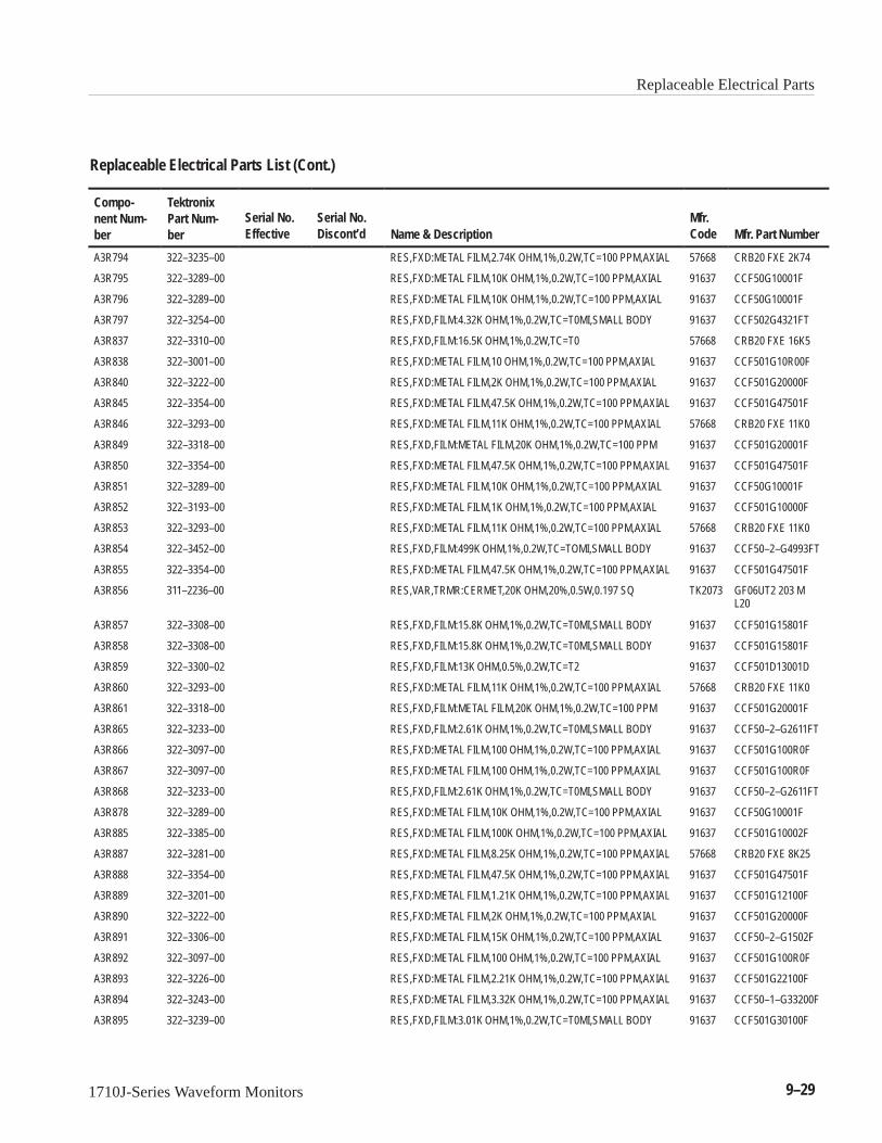
Replaceable Electrical Parts
1710J-Series Waveform Monitors 9–29
Replaceable Electrical Parts List (Cont.)
Compo-nent Num-ber Mfr. Part Number
Mfr.CodeName & Description
Serial No.Discont’d
Serial No.Effective
TektronixPart Num-ber
A3R794 322–3235–00 RES,FXD:METAL FILM,2.74K OHM,1%,0.2W,TC=100 PPM,AXIAL 57668 CRB20 FXE 2K74
A3R795 322–3289–00 RES,FXD:METAL FILM,10K OHM,1%,0.2W,TC=100 PPM,AXIAL 91637 CCF50G10001F
A3R796 322–3289–00 RES,FXD:METAL FILM,10K OHM,1%,0.2W,TC=100 PPM,AXIAL 91637 CCF50G10001F
A3R797 322–3254–00 RES,FXD,FILM:4.32K OHM,1%,0.2W,TC=T0MI,SMALL BODY 91637 CCF502G4321FT
A3R837 322–3310–00 RES,FXD,FILM:16.5K OHM,1%,0.2W,TC=T0 57668 CRB20 FXE 16K5
A3R838 322–3001–00 RES,FXD:METAL FILM,10 OHM,1%,0.2W,TC=100 PPM,AXIAL 91637 CCF501G10R00F
A3R840 322–3222–00 RES,FXD:METAL FILM,2K OHM,1%,0.2W,TC=100 PPM,AXIAL 91637 CCF501G20000F
A3R845 322–3354–00 RES,FXD:METAL FILM,47.5K OHM,1%,0.2W,TC=100 PPM,AXIAL 91637 CCF501G47501F
A3R846 322–3293–00 RES,FXD:METAL FILM,11K OHM,1%,0.2W,TC=100 PPM,AXIAL 57668 CRB20 FXE 11K0
A3R849 322–3318–00 RES,FXD,FILM:METAL FILM,20K OHM,1%,0.2W,TC=100 PPM 91637 CCF501G20001F
A3R850 322–3354–00 RES,FXD:METAL FILM,47.5K OHM,1%,0.2W,TC=100 PPM,AXIAL 91637 CCF501G47501F
A3R851 322–3289–00 RES,FXD:METAL FILM,10K OHM,1%,0.2W,TC=100 PPM,AXIAL 91637 CCF50G10001F
A3R852 322–3193–00 RES,FXD:METAL FILM,1K OHM,1%,0.2W,TC=100 PPM,AXIAL 91637 CCF501G10000F
A3R853 322–3293–00 RES,FXD:METAL FILM,11K OHM,1%,0.2W,TC=100 PPM,AXIAL 57668 CRB20 FXE 11K0
A3R854 322–3452–00 RES,FXD,FILM:499K OHM,1%,0.2W,TC=TOMI,SMALL BODY 91637 CCF50–2–G4993FT
A3R855 322–3354–00 RES,FXD:METAL FILM,47.5K OHM,1%,0.2W,TC=100 PPM,AXIAL 91637 CCF501G47501F
A3R856 311–2236–00 RES,VAR,TRMR:CERMET,20K OHM,20%,0.5W,0.197 SQ TK2073 GF06UT2 203 ML20
A3R857 322–3308–00 RES,FXD,FILM:15.8K OHM,1%,0.2W,TC=T0MI,SMALL BODY 91637 CCF501G15801F
A3R858 322–3308–00 RES,FXD,FILM:15.8K OHM,1%,0.2W,TC=T0MI,SMALL BODY 91637 CCF501G15801F
A3R859 322–3300–02 RES,FXD,FILM:13K OHM,0.5%,0.2W,TC=T2 91637 CCF501D13001D
A3R860 322–3293–00 RES,FXD:METAL FILM,11K OHM,1%,0.2W,TC=100 PPM,AXIAL 57668 CRB20 FXE 11K0
A3R861 322–3318–00 RES,FXD,FILM:METAL FILM,20K OHM,1%,0.2W,TC=100 PPM 91637 CCF501G20001F
A3R865 322–3233–00 RES,FXD,FILM:2.61K OHM,1%,0.2W,TC=T0MI,SMALL BODY 91637 CCF50–2–G2611FT
A3R866 322–3097–00 RES,FXD:METAL FILM,100 OHM,1%,0.2W,TC=100 PPM,AXIAL 91637 CCF501G100R0F
A3R867 322–3097–00 RES,FXD:METAL FILM,100 OHM,1%,0.2W,TC=100 PPM,AXIAL 91637 CCF501G100R0F
A3R868 322–3233–00 RES,FXD,FILM:2.61K OHM,1%,0.2W,TC=T0MI,SMALL BODY 91637 CCF50–2–G2611FT
A3R878 322–3289–00 RES,FXD:METAL FILM,10K OHM,1%,0.2W,TC=100 PPM,AXIAL 91637 CCF50G10001F
A3R885 322–3385–00 RES,FXD:METAL FILM,100K OHM,1%,0.2W,TC=100 PPM,AXIAL 91637 CCF501G10002F
A3R887 322–3281–00 RES,FXD:METAL FILM,8.25K OHM,1%,0.2W,TC=100 PPM,AXIAL 57668 CRB20 FXE 8K25
A3R888 322–3354–00 RES,FXD:METAL FILM,47.5K OHM,1%,0.2W,TC=100 PPM,AXIAL 91637 CCF501G47501F
A3R889 322–3201–00 RES,FXD:METAL FILM,1.21K OHM,1%,0.2W,TC=100 PPM,AXIAL 91637 CCF501G12100F
A3R890 322–3222–00 RES,FXD:METAL FILM,2K OHM,1%,0.2W,TC=100 PPM,AXIAL 91637 CCF501G20000F
A3R891 322–3306–00 RES,FXD:METAL FILM,15K OHM,1%,0.2W,TC=100 PPM,AXIAL 91637 CCF50–2–G1502F
A3R892 322–3097–00 RES,FXD:METAL FILM,100 OHM,1%,0.2W,TC=100 PPM,AXIAL 91637 CCF501G100R0F
A3R893 322–3226–00 RES,FXD:METAL FILM,2.21K OHM,1%,0.2W,TC=100 PPM,AXIAL 91637 CCF501G22100F
A3R894 322–3243–00 RES,FXD:METAL FILM,3.32K OHM,1%,0.2W,TC=100 PPM,AXIAL 91637 CCF50–1–G33200F
A3R895 322–3239–00 RES,FXD,FILM:3.01K OHM,1%,0.2W,TC=T0MI,SMALL BODY 91637 CCF501G30100F
Replaceable Electrical Parts
9–30 1710J-Series Waveform Monitors
Replaceable Electrical Parts List (Cont.)
Compo-nent Num-ber Mfr. Part Number
Mfr.CodeName & Description
Serial No.Discont’d
Serial No.Effective
TektronixPart Num-ber
A3R896 322–3258–00 RES,FXD:METAL FILM,4.75K OHM,1%,0.2W,TC=100 PPM,AXIAL 56845 CCF50–2–G4751FT
A3R897 322–3226–00 RES,FXD:METAL FILM,2.21K OHM,1%,0.2W,TC=100 PPM,AXIAL 91637 CCF501G22100F
A3R898 322–3306–00 RES,FXD:METAL FILM,15K OHM,1%,0.2W,TC=100 PPM,AXIAL 91637 CCF50–2–G1502F
A3R899 322–3289–00 RES,FXD:METAL FILM,10K OHM,1%,0.2W,TC=100 PPM,AXIAL 91637 CCF50G10001F
A3R900 322–3193–00 RES,FXD:METAL FILM,1K OHM,1%,0.2W,TC=100 PPM,AXIAL 91637 CCF501G10000F
A3R901 322–3164–00 672–1333–10 RES,FXD,FILM:499 OHM,1%,0.2W,TC=T0MI,SMALL BODY 91637 CCF501G499ROF
A3R901 322–3175–00 672–1333–11 RES,FXD,FILM:649 OHM,1%,0.2W,TC=T0,SMALL BODY 57668 CRB20 FXE 649E
A3R901 322–3164–00 672–1465–00 RES,FXD,FILM:499 OHM,1%,0.2W,TC=T0MI,SMALL BODY 91637 CCF501G499ROF
A3R901 322–3175–00 672–1465–01 RES,FXD,FILM:649 OHM,1%,0.2W,TC=T0,SMALL BODY 57668 CRB20 FXE 649E
A3R902 322–3164–00 672–1333–10 RES,FXD,FILM:499 OHM,1%,0.2W,TC=T0MI,SMALL BODY 91637 CCF501G499ROF
A3R902 322–3175–00 672–1333–11 RES,FXD,FILM:649 OHM,1%,0.2W,TC=T0,SMALL BODY 57668 CRB20 FXE 649E
A3R902 322–3164–00 672–1465–00 RES,FXD,FILM:499 OHM,1%,0.2W,TC=T0MI,SMALL BODY 91637 CCF501G499ROF
A3R902 322–3175–00 672–1465–01 RES,FXD,FILM:649 OHM,1%,0.2W,TC=T0,SMALL BODY 57668 CRB20 FXE 649E
A3R903 322–3222–00 RES,FXD:METAL FILM,2K OHM,1%,0.2W,TC=100 PPM,AXIAL 91637 CCF501G20000F
A3R904 322–3289–00 RES,FXD:METAL FILM,10K OHM,1%,0.2W,TC=100 PPM,AXIAL 91637 CCF50G10001F
A3R905 322–3231–00 RES,FXD,FILM:2.49K OHM,1%,0.2W,TC=T0MI,SMALL BODY 57668 CRB20 FXE 2K49
A3R906 322–3231–00 RES,FXD,FILM:2.49K OHM,1%,0.2W,TC=T0MI,SMALL BODY 57668 CRB20 FXE 2K49
A3R938 322–3289–00 RES,FXD:METAL FILM,10K OHM,1%,0.2W,TC=100 PPM,AXIAL 91637 CCF50G10001F
A3R940 322–3289–00 RES,FXD:METAL FILM,10K OHM,1%,0.2W,TC=100 PPM,AXIAL 91637 CCF50G10001F
A3R944 322–3391–00 B040332 RES,FXD,FILM:115K OHM,1%,0.2W,TC=T0MI,SMALL BODY 91637 CCF50–2–G11502FT
A3R944 322–3385–00 B040333 RES,FXD:METAL FILM,100K OHM,1%,0.2W,TC=100PPM,AXIAL,T&R,SMALL BODY
57668 CRB20T29EFX1003
A3R944 322–3391–00 B040332 RES,FXD,FILM:115K OHM,1%,0.2W,TC=T0MI,SMALL BODY 91637 CCF50–2–G11502FT
A3R944 322–3385–00 B040333 RES,FXD:METAL FILM,100K OHM,1%,0.2W,TC=100PPM,AXIAL,T&R,SMALL BODY
57668 CRB20T29EFX1003
A3R947 322–3421–00 RES,FXD,FILM:237K OHM,1%,0.2W,TC=T0 MI,SMALL BODY 91637 CCF50–2F23702F
A3R951 322–3066–00 RES,FXD:METAL FILM,47.5 OHM,1%,0.2W,TC=100 PPM,AXIAL 09969 CCF502G47R50F
A3R953 322–3481–00 RES,FXD,FILM:1M OHM.1%,0.2W,TC=T0MI,SMALL BODY 57668 CRB20 FXE 1M00
A3R954 322–3435–00 RES,FXD:METAL FILM,332K OHM,1%,0.2W,TC=100 PPM,AXIAL 91637 CCF50–2–33202FT
A3R956 322–3258–00 RES,FXD:METAL FILM,4.75K OHM,1%,0.2W,TC=100 PPM,AXIAL 56845 CCF50–2–G4751FT
A3R957 322–3318–00 RES,FXD,FILM:METAL FILM,20K OHM,1%,0.2W,TC=100 PPM 91637 CCF501G20001F
A3R958 322–3385–00 RES,FXD:METAL FILM,100K OHM,1%,0.2W,TC=100 PPM,AXIAL 91637 CCF501G10002F
A3R959 322–3385–00 RES,FXD:METAL FILM,100K OHM,1%,0.2W,TC=100 PPM,AXIAL 91637 CCF501G10002F
A3R960 322–3385–00 RES,FXD:METAL FILM,100K OHM,1%,0.2W,TC=100 PPM,AXIAL 91637 CCF501G10002F
A3R963 322–3243–00 RES,FXD:METAL FILM,3.32K OHM,1%,0.2W,TC=100 PPM,AXIAL 91637 CCF50–1–G33200F
A3R964 322–3481–00 RES,FXD,FILM:1M OHM.1%,0.2W,TC=T0MI,SMALL BODY 57668 CRB20 FXE 1M00
A3R965 322–3385–00 RES,FXD:METAL FILM,100K OHM,1%,0.2W,TC=100 PPM,AXIAL 91637 CCF501G10002F

Replaceable Electrical Parts
1710J-Series Waveform Monitors 9–31
Replaceable Electrical Parts List (Cont.)
Compo-nent Num-ber Mfr. Part Number
Mfr.CodeName & Description
Serial No.Discont’d
Serial No.Effective
TektronixPart Num-ber
A3R966 322–3354–00 RES,FXD:METAL FILM,47.5K OHM,1%,0.2W,TC=100 PPM,AXIAL 91637 CCF501G47501F
A3R987 322–3273–00 RES,FXD:METAL FILM,6.81K OHM,1%,0.2W,TC=100 PPM,AXIAL 91637 CCF50–2–G68100F
A3R988 322–3322–00 RES,FXD:METAL FILM,22.1K OHM,1%,0.2W,TC=100 PPM,AXIAL 57668 CRB20 FXE 22K1
A3R989 322–3250–00 RES,FXD:METAL FILM,3.92K OHM,1%,0.2W,TC=100 PPM,AXIAL 91637 CCF50–2F39200F
A3R990 322–3250–00 RES,FXD:METAL FILM,3.92K OHM,1%,0.2W,TC=100 PPM,AXIAL 91637 CCF50–2F39200F
A3R991 322–3385–00 RES,FXD:METAL FILM,100K OHM,1%,0.2W,TC=100 PPM,AXIAL 91637 CCF501G10002F
A3R992 322–3418–00 RES,FXD:METAL FILM,221K OHM,1%,0.2W,TC=100 PPM,AXIAL 57668 CRB20 FXE 221K
A3R993 322–3289–00 RES,FXD:METAL FILM,10K OHM,1%,0.2W,TC=100 PPM,AXIAL 91637 CCF50G10001F
A3R994 322–3322–00 RES,FXD:METAL FILM,22.1K OHM,1%,0.2W,TC=100 PPM,AXIAL 57668 CRB20 FXE 22K1
A3R997 322–3306–00 RES,FXD:METAL FILM,15K OHM,1%,0.2W,TC=100 PPM,AXIAL 91637 CCF50–2–G1502F
A3U164 156–1451–00 IC,LINEAR:BIPOLAR,VOLTAGE REGULATOR,NEGATIVE,ADJUST 01295 LM337KC
A3U172 156–1161–00 IC,LINEAR:BIPOLAR,VOLTAGE REGULATOR,POSITIVE,ADJUST 04713 LM317T
A3U234 156–0941–00 IC,DIGITAL:CMOS,GATE,QUAD 2–INPUT NAND,74C00,DIP14.3 27014 MM74C00N
A3U252 156–0048–00 IC,LINEAR:BIPOLAR,XSTR ARRAY,(5),NPN,(1)DIFF PAIR,(3)IND 04713 MC3346P
A3U263 156–1225–00 IC,LINEAR:BIPOLAR,COMPARATOR,DUAL,OPEN COLLECTOR 01295 LM393P
A3U277 156–1850–00 IC,MISC:CMOS,ANALOG SWITCH,QUAD,DG211,DIP16.3 17856 DG211CJ
A3U305 156–0259–00 IC,LINEAR:BIPOLAR,TRANSISTOR ARRAY,(5)NPN 0CVK3 ULN2083A
A3U331 156–0910–00 IC,DIGITAL:LSTTL,COUNTER,DUAL 4–BIT DECADE 01295 SN74LS390N
A3U334 156–0575–00 IC,DIGITAL:CMOS,GATE,TRIPLE 3–INPUT NOR 04713 MC14025BCP
A3U395 156–1850–00 IC,MISC:CMOS,ANALOG SWITCH,QUAD,DG211,DIP16.3 17856 DG211CJ
A3U407 156–1430–00 IC,DIGITAL:CMOS,MISC,4–DIGIT LED DISPLAY CONTROLLER 27014 MM74C911N
A3U445 156–1225–00 IC,LINEAR:BIPOLAR,COMPARATOR,DUAL,OPEN COLLECTOR 01295 LM393P
A3U465 156–1225–00 IC,LINEAR:BIPOLAR,COMPARATOR,DUAL,OPEN COLLECTOR 01295 LM393P
A3U488 156–1149–00 IC,LINEAR:BIFET,OP–AMP,LF351N,DIP08.3 04713 MC34001P/LF351N
A3U492 156–2460–00 IC,MISC:BIPOLAR,MODULATOR/DEMODULATOR,BALANCED 04713 MC1496P
A3U495 156–1191–00 IC,LINEAR:BIFET,OP–AMP,DUAL,TL072CN/LF353N,DIP08.3 01295 TL072CP
A3U522 160–7318–00 MICROCKT,DGTL:CMOS,MICROCOMPUTER,8 BIT,PRGM 80009 160–7318–00
*MOUNTING PARTS*
136–0871–00 SOCKET,PLCC::PCB,68 POS,0.05 CTR,0.360H X 0.125 TAIL 00779 3–821574–1
*END MOUNTING PARTS*
A3U541 156–2009–00 IC,DIGITAL:HCMOS,FLIP FLOP,DUAL D–TYPE,SET,CLEAR 01295 SN74HC74N
A3U552 156–1191–00 IC,LINEAR:BIFET,OP–AMP,DUAL,TL072CN/LF353N,DIP08.3 01295 TL072CP
A3U564 156–0048–00 IC,LINEAR:BIPOLAR,TRANSISTOR ARRAY,(5),NPN,(1)DIFF PAIR 04713 MC3346P
A3U578 156–2460–00 IC,MISC:BIPOLAR,MODULATOR/DEMODULATOR,BALANCED 04713 MC1496P
A3U585 156–1850–00 IC,MISC:CMOS,ANALOG SWITCH,QUAD,DG211,DIP16.3 17856 DG211CJ
A3U655 156–1191–00 IC,LINEAR:BIFET,OP–AMP,DUAL,TL072CN/LF353N,DIP08.3 01295 TL072CP
A3U735 160–7332–01 IC,DIGITAL:STTL,PLD,PAL,20R4,28.5MHZ,210MA,PRGM 80009 160–7332–01
*MOUNTING PARTS*

Replaceable Electrical Parts
9–32 1710J-Series Waveform Monitors
Replaceable Electrical Parts List (Cont.)
Compo-nent Num-ber Mfr. Part Number
Mfr.CodeName & Description
Serial No.Discont’d
Serial No.Effective
TektronixPart Num-ber
136–0727–00 SKT,PL–IN ELEK:MICROCKT,8 CONTACT MI 98291 DIPS08PIT
*END MOUNTING PARTS*
A3U741 156–0750–03 672–1333–12 IC,DIGITAL:CMOS,MULTIVIBRATOR,DUAL MONOSTABLE 27014 MM74C221N
A3U741 156–2761–01 672–1333–13 IC,DIGITAL:HCMOS,MULTIVIBRATOR,DUPLICATE OF156–2761–00,74HC221A,DIP16.3,TUBE
0JR04 TC74HC221AP
A3U741 156–0750–03 672–1465–02 IC,DIGITAL:CMOS,MULTIVIBRATOR,DUAL MONOSTABLE 27014 MM74C221N
A3U741 156–2761–01 672–1465–03 IC,DIGITAL:HCMOS,MULTIVIBRATOR,DUPLICATE OF156–2761–00,74HC221A,DIP16.3,TUBE
0JR04 TC74HC221AP
A3U753 156–1225–00 IC,LINEAR:BIPOLAR,COMPARATOR,DUAL,OPEN COLLECTOR 01295 LM393P
A3U786 156–3972–00 IC,MISC:CMOS,ANALOG SWITCH,QUAD SPST,100 OHM,400NS 17856 DG444DJ
A3U795 156–0048–00 IC,LINEAR:BIPOLAR,TRANSISTOR ARRAY,(5),NPN,(1)DIFF PAIR 04713 MC3346P
A3U809 156–3142–00 IC,DIGITAL:HCTCMOS,GATE,QUAD 2–INPUT NAND 01295 SN74HCT00N
A3U844 156–0750–03 672–1333–12 IC,DIGITAL:CMOS,MULTIVIBRATOR,DUAL MONOSTABLE 27014 MM74C221N
A3U844 156–2761–01 672–1333–13 IC,DIGITAL:HCMOS,MULTIVIBRATOR,DUPLICATE OF156–2761–00,74HC221A,DIP16.3,TUBE
0JR04 TC74HC221AP
A3U844 156–0750–03 672–1465–02 IC,DIGITAL:CMOS,MULTIVIBRATOR,DUAL MONOSTABLE 27014 MM74C221N
A3U844 156–2761–01 672–1465–03 IC,DIGITAL:HCMOS,MULTIVIBRATOR,DUPLICATE OF156–2761–00,74HC221A,DIP16.3,TUBE
0JR04 TC74HC221AP
A3U892 156–1381–00 IC,LINEAR:BIPOLAR,TRANSISTOR ARRAY,THREE NPN 34371 CA3096AE
A3U947 156–1191–00 IC,LINEAR:BIFET,OP–AMP,DUAL,TL072CN/LF353N,DIP08.3 01295 TL072CP
A3VR273 152–0273–00 SEMICOND DVC,DI:TAB,LEAD SPIDER 80009 152–0273–00
A3VR297 152–0175–00 DIODE,ZENER:5.6V,5%,0.4W,1N752A,DO–7OR 35,TR 04713 SZG35008(1N752ARL)
A3VR460 152–0217–00 DIODE,ZENER:8.2V,5%,0.4W,1N959B FMLY,DO–35 OR 7,T&R 04713 SZG20RL
A3VR497 152–0175–00 DIODE,ZENER:5.6V,5%,0.4W,1N752A,DO–7OR 35,TR 04713 SZG35008(1N752ARL)
A3VR769 152–0359–00 DIODE,ZENER:9V,500MW,5%,TEMP COMPENSATED 04713 SZ50850
A3W786 131–0566–00 BUS,CONDUCTOR:DUMMY RES,0.094 OD X 0.225 L 24546 OMA0207
A3Y709 158–0300–00 XTAL UNIT,QTZ:12.0 MHZ,50 PPM 61429 FOX120X
A3A1 671–1796–01 CIRCUIT BD ASSY:GRATICULE LIGHT 80009 671–1796–01
A3A1DS100 150–0168–00 LAMP,INCAND:14V,0.08A,WG BASE,T1.75 FOR SKT MT 80009 150–0168–00
*MOUNTING PARTS*
136–1119–01 SOCKET,LPHLDR:PCB,LAMPHOLDER,FEMALE,STR 80009 136–1119–01
*END MOUNTING PARTS*
A3A1DS200 150–0168–00 LAMP,INCAND:14V,0.08A,WG BASE,T1.75 FOR SKT MT 80009 150–0168–00
*MOUNTING PARTS*
136–1119–01 SOCKET,LPHLDR:PCB,LAMPHOLDER,FEMALE,STR 80009 136–1119–01
*END MOUNTING PARTS*
A3A1DS300 150–0168–00 LAMP,INCAND:14V,0.08A,WG BASE,T1.75 FOR SKT MT 80009 150–0168–00

Replaceable Electrical Parts
1710J-Series Waveform Monitors 9–33
Replaceable Electrical Parts List (Cont.)
Compo-nent Num-ber Mfr. Part Number
Mfr.CodeName & Description
Serial No.Discont’d
Serial No.Effective
TektronixPart Num-ber
*MOUNTING PARTS*
136–1119–01 SOCKET,LPHLDR:PCB,LAMPHOLDER,FEMALE,STR 80009 136–1119–01
*END MOUNTING PARTS*
A3A1J100 131–4530–00 CONN,HDR: 80009 131–4530–00
A3A1P100 131–3199–00 CONN,SHUNT:FEM,STR,1 X 2,0.1 CTR,0.2 H,LOW PF,JUMPER 22526 76264–101
A3A1P200 131–2790–00 CONN,HDR:PCB;RTANG,1 X 2,0.15 CTR 80009 131–2790–00
A3A1P800 131–2790–00 CONN,HDR:PCB;RTANG,1 X 2,0.15 CTR 80009 131–2790–00
A10 671–3637–00 CIRCUIT BD ASSY:CRT SOCKET BD 80009 671363700
V1 154–0985–00 ELECTRON TUBE:CRT,FINISHED,D14–375GH/985(1710J ONLY)
80009 154–0985–00
V1 154–0985–16 ELECTRON,TUBE:CRT,FINISHED,D14–375WA/985(1710J OPTION 74 ONLY)
80009 154–0985–16
V1 154–0986–00 ELECTRON TUBE:CRT,FINISHED,D14–375GH/986(1711J ONLY)
80009 154–0986–00
V1 154–0986–16 ELECTRON,TUBE:CRT,FINISHED,D14–375WA/986(1711J OPTION 74 ONLY)
80009 154–0986–16
W3 196–3146–00 CA ASSY,SP:FLAT FLEX,FLX,27 AWG,1.0 L,PCB,TERM(CONNECTED AT A3J3 AND ”CH-A” BNC)
TK0196 FSN–1A,P OR K
W6 196–3146–00 CA ASSY,SP:FLAT FLEX,FLX,27 AWG,1.0 L,PCB,TERM(CONNECTED AT A3J6 AND ”CH-B” BNC)
TK0196 FSN–1A,P OR K
W9 196–3146–00 CA ASSY,SP:FLAT FLEX,FLX,27 AWG,1.0 L,PCB,TERM(CONNECTED AT A3J9 AND ”EXT REF” BNC)
TK0196 FSN–1A,P OR K
W100 196–3146–00 CA ASSY,SP:FLAT FLEX,FLX,27 AWG,1.0 L,PCB,TERM(CONNECTED AT A3J100 AND ”CH-B” BNC GROUND LUG)
TK0196 FSN–1A,P OR K

Replaceable Electrical Parts
9–34 1710J-Series Waveform Monitors

Diagrams


1710J-Series Waveform Monitors 10–1
Diagrams/Circuit Board Illustrations
SymbolsGraphic symbols and class designation letters are based on ANSI StandardY32.2–1975.
Logic symbology is based on ANSI Y32.14–1973 in terms of positive logic.Logic symbols depict the logic function performed and may differ from themanufacturer’s data.
Overline, parenthesis, or leading slash indicate a low asserting state.
Example: ID CONTROL, (ID CONTROL), or /ID CONTROL.
Abbreviations are based on ANSI Y1.1–1972.
Other ANSI standards that are used in the preparation of diagrams by Tektronix,Inc. are:
Y14.15, 1966 — Drafting Practices.Y14.2, 1973 — Line Conventions and Lettering.Y10.5, 1968 — Letter Symbols for Quantities Used in Electrical Science
and Electrical Engineering.
American National Standard Institute1430 Broadway, New York, New York 10018
Component ValuesElectrical components shown on the diagrams are in the following units unlessnoted otherwise:
Capacitors = Values one or greater are in picofarads (pF).Values less than one are in microfarads (F).
Resistors = Ohms ().
The following information and special symbols may appear in this manual.

Diagrams/Circuit Board Illustrations
10–2 1710J-Series Waveform Monitors
Assembly NumbersEach assembly in the instrument is assigned an assembly number (e.g., A20).The assembly number appears on the diagram (in circuit board outline), circuitboard illustration title, and lookup table for the schematic diagram.
The Replaceable Electrical Parts List is arranged by assembly number innumerical sequence; the components are listed by component number. Example:
Chassis–mounted componentshave no Assembly No. prefix.See end of Replaceable ElectricalParts List
AssemblyNumber
Component Number
Schematic Circuit
Number
Grid CoordinatesThe schematic diagram and circuit board component location illustration havegrids. A lookup table with the grid coordinates is provided for ease of locatingthe component. Only the components illustrated on the facing diagram are listedin the lookup table.
When more than one schematic diagram is used to illustrate the circuitry on acircuit board, the circuit board illustration will only appear opposite the firstdiagram; the lookup table will list the diagram number of other diagrams that theother circuitry appears on.
(#$%#!
&
!&
! %'
! #%$
%)!
!#%
'
&! #
%#' %
#
'
##
!
!&%
!
# %!
%&#
&
&
'
#
# %%
%$
##%
(' #
#
"
(
' '
'
%!
'
'
#
($
&$%%
(
#
$%
##
!#%
#
#
$
$!#%$$%
#$%
#%#
$"&#!
% #
!#% #
#
"
'
$!#%$$% #
##'&$
$#&##$
&
$#(#'#
&$%%
#&% #
&%
$&#
$#'
%%
&%
$%#&%
$%&# $$)&#
'#%!&%
! % % ##

CH A
CH B
REMOTE<5>
S/H<1>
SYNC STRIP<1>
FRONTPANEL
<6>
H.V. SUPPLY<8>
Z-AXISCONTROL
<3>
S/H<1>
INPUTAMP
EXTREF
INPUTAMP
COMPSYNC
/EXT
/LPASS
FLAT<1>
LOW PASS<1>
/3.58or
/4.43
/B
/FLAT
BAND PASS<1>
GAIN CELL<2>
CAL<1>
MICROCONTROLLER<2>
<2>
S/H<2>
<2> LIMITER<2>
VCAL
X5
19
TIMINGSTATE
MACHINE<3>
FOCUSAMP <8>B P GEN
<3>
9
<5>
/RGB
HORZ SYNC<3>
VERT SYNC<3>
H.V. TRIG
FIELD/HSYNC
SWEEP GEN<4>
RGB STAIRCASE YRGB/RGB<4>
LIN/FLD
BLANKING
INTENS
MAG AMP<4>
OUTPUTAMP <4>
HORIZONTALDEFLECTION toCRT
FOCUS
CRT<8>
+100 V+40 V+15 V
+5 V–15 V
MULT<8>
GRID
CATH
TRACE ROT<3>
ROTATE
GRAT LIGHTS<3>
SCALE
POSTANODE
LOW VOLTSSUPPLY
<7>
3 TERMREGS<3>
+11.8 V
–11.8 V
HMAG1 &HMAG2
OUTPUTAMP <2>
VERTICALDEFLECTION toCRT
POWERINPUT
VERTICALPOSITION
HORIZONTALPOSITION
/BP
/BP
/RGBEN
CALDR /BP/CAL
Z-AXISAMP <8>
INPUTAMP
Figure 10–1: 1710J–Series Block diagram

"! #
Assembly A3
A3 Main Board Schematic <1>Component Locator
A3 Main Board
1710J–Series Waveform MonitorsFigure 10–2: A3 Main Board Schematic <1> component locator

&
'
#
"
'
#
!
'
'
#
#
'
#
&
&
'
#
&
&
'
'
#
'#
&
!
!
$
'
'
#
#
!
"
#
!
#
#
"
"
!
&!
'
'
'
#
#
#
#
#
" "
&
'
'
''
'
#
#
"
"
!
!
!
&
&
#
#
#
# #
"
!
$+
'
#
#
!
'
#
&
!
!
!
'
#
#
#
"
&
"
&
&
&
'
#
#
&
!
#
'
##
#
#
!
'
'#
#
#
#
#
"
!
+#
&
&
'
'#
#
#
#
&
&
+#
'
'
#
&%
&
&
&
'
'
'
'
#
#
#
#
#
'
#
#
#
#"
&
&
&
&
'
'
#
#
&
'
#
# !
!
!
#
#
#
#
&
& (
!$$
%
'
'
#
#
#
#
"
#
"
#
#
$
'
#
#
&
&
#
#
#
#
&
&
&
&
! #
#
&%
#
&
!
'
'#
#
"
"
#
!
!
&
!
'
'
#
#
#
&
"
'#
#
#
#
&
&
#
"
#
#
#
&
&
'
'
'
'
#
#
#
&
#
!
&
'
'
'#
#
#
#
#
!+$*
'
#
#
&
&
#
&
'
'
#
#
#
&
"
#
#
#
''
# #
#
#
&
#
#
"
&
&
)%
'
'
'
#
#
#
#
#
&
'
#
&
!
' ''
'
FILTER SELECTION
' !
INPUT AMPLIFIERS##!
!&%
(
!&% &!
CALIBRATOR
%$
!
!
!
##!
CHANNEL SWITCH
! !
!
!$$ !$$
& SOURCE SWITCHEXTERNAL SYNC INPUT
##!
!&%
(
(
!
'
SYNC STRIPPER
&!
!&%
)%#
##
(
1710J WAVEFORM MONITOR
!
$//7,8:9329:068/,82/8<,3;/9,5.9/82,35;4-/88,51/9
VERTICAL INPUT <1>
!#% #

Assembly A3
A3 Main Board Schematic <2> Component Locator
Figure 10–3: A3 Main Board Schematic <2> component locator1710J–Series Waveform Monitors

&
'
'
#
#
#
#
&
'
#
'
&
# (
&
#
#
#
#
&
&
&
'
#
#
#
#
"
&
'
# #
&
#
#
"
&
& !
'
#
#
#
#
#
#
$*
'
#
#
#
#
#"
&
&
''
# #
#
!
!
'
#
#
"
#
!
&
'
''
#
#
"
"
#
"
'
'
#
#
#
#
!
!
'
#
#" "
" "
'
#
#
&
''
#
#
#
"
!
#
#
#
# #
#
#
!
'
'
#
#
#
#
#
"
!
!
'
#
#
#
#
#
&
!
#
'! $
#
#
#
#
'
'
*#
&
&
&
)
'
'
#
#
!
&
''
#
#
#
'#
"
#
&
!
'
'
#
#
#
"
&
&
''
#
&
&
&
''
'
'
&
&
'
#
#
#
&
&
&
! #
'
&
#
#
' GAIN CELL
GAIN CELLAMPLIFIER
VERTICALOUTPUT
AMPLIFIER
%% #%
#
SWITCHABLE GAIN AMPLIFIER
'#%%
%%#
##
!
2nd DC RESTORER
$ ($%
#$% ##
'
)#$%#
) !
1710J WAVEFORM MONITOR
$..6+7982189/57.+71.7;+2:.8+4-8.71+24:3,.77+40.8
VERTICAL OUTPUT <2>
!#% #
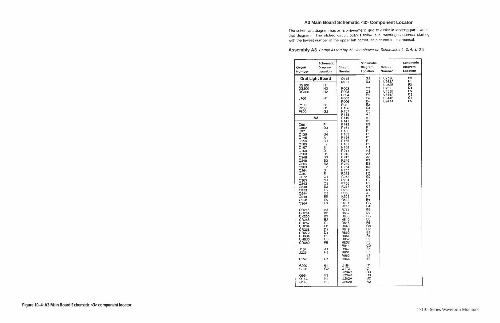
Assembly A3
A3 Main Board Schematic <3> Component Locator
Figure 10–4: A3 Main Board Schematic <3> component locator1710J–Series Waveform Monitors

&
%#
%#+
"
"
"
*+(#
&
&
&
&
&
%
%
&
%$
%
&
"
%
%
"
"
"
"
%
%$
%
&
&
"
%
%
" "
"
"
%
&&
&
"
""
"
"
%
%
%
&
"
"&
"
!
%
%
%
#
"
"
&
&
"
%
&
"
"
"
&
"
"
%
%
"
$#
$# %
%
&
"
"
"
%
"
&
"
"
"
!(
"(
!
!
%
%
"
&
&
"
"
"
!
"
%
& &
&
&
"
"
"
!
!+$"
$+
&
"
%
"
"
+#)
$+#
$
"
%"
%
&
&
(
"(
!
!
%
;
&
"
&
"
"
$#
#)
&
"
+#
"
#'
##+#
"+
+# &+$"
$
##
+
&
"
"
"
%
&
"
%
%
&
&
"
"
" "
"
"
&
& &
&
"
"
"
%$
%
"
GRATICULE ILLUMINATION
+11.8V REGULATORS+
$"
'"#% )
' '
%$
&
%$
&#%
&
$
#
"$
#
#
#
"$%$"
Z AXISCONTROL
H SYNCGENERATOR
TRACE ROTATION
'
$#$"$
"$$
"$
$
GENERATORVERTICAL SYNC
"$
"$
#)+#
1710J WAVEFORM MONITOR TIMING & CONTROL CIRCUIT <3>
#//7,8:9329:068/,82/8<,3;/9,5.9/82,35;4-/88,51/9 "$"

E1
Assembly A3
A3 Main Board Schematic <4> Component Locator
Figure 10–5: A3 Main Board Schematic <4> component locator1710J–Series Waveform Monitors

)
)
%
)
)
%
!.
(
(
#"&!
%
(
(
&'%
%
%
%
( ' %
)
)
)
%
%
%
%
(
%
$
%
(
(
)
)
%
%
(
!
'.
(
#
)
%
%
(
%
#
%
%
%
%
( '
$
#
#
)
%
%
%
%
%
(
#
)
%
%
%
+
%+
$
$
(
(
.'%
)
)
%
%
$
$
#%
(
)
%
)
%
%
%
(
) )
%
""
)
)
(
%
#
(
)
)
%
%
%
%
#
)
)
%
%
%
%
%
( '
$
#
)
%
%
%
%
%
%
(
)
)
%
%
$
)%
%
%
$
%
%
%
)
%
(
)
%
%
#
%
%
%
$ $
)
%
%
%
%
(
)
$
#
)
'*"."!
))
%
%
%
%
(
)
(
+
%+
$
$
(
).'%
)
%
%
$
$
#%
(
(
)
)
%
%
$
%
%
%
$
)
)
% %
%
%
%
$
))
%
%
%
$
%
$
)
%
)(
(
)
)
)
)
%
%
%
% %
$
%
%
)
)
)
%
% %%
%
$
(
%.!
,%%
))
%
%
)%%
(
(
)
)
%
( '
)
%
)
MAGNIFIER &POSITION AMPLIFIER
SWEEPGENERATOR
!
OUTPUTAMPLIFIER
HORIZONTAL
!
!
%'
%'
!
!
!
@@
&*#!'
)
"!!''"%'
%!
%
"%-"!''"!
>&
%
>&
!
!
)
%'
$
&
1710J WAVEFORM MONITOR SWEEP GENERATORS & HORIZ OUTPUT <4>
&22:/;=<65<=39;2/;52;?/6>2</81<2;5/68>702;;/842< #%'" !"%

Assembly A3
A3 Main Board Schematic <5> Component Locator
Figure 10–6: A3 Main Board Schematic <5> component locator1710J–Series Waveform Monitors
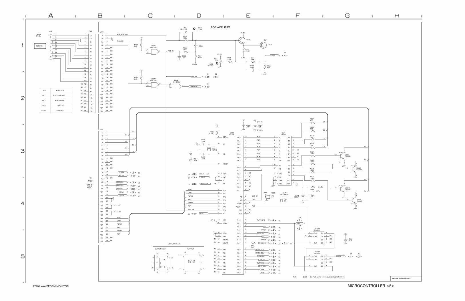
*
%
&#!$
&!$ &$
&!
&/'(&'
$
&&$"
&!#(
"
"
"
"
"
"
"
"
"
&/"
*
*
&
&
)(
&#'(
)
&/"
&/"
*
&
&
&
$
'(&*
*
*
&
&
&
&
&
%
-&&
)(
"
"
"
"
"
"
"
"
"
"
"
)(
"
"
"
"
"
"
"
"
"
)"(#"
&'(&'
&"
&#)"
-&&
$"
$"
$"
$"
&
&
&
$
$
-!.
$"
$"
)
)
*
*
*
&
*$
,
,
&'(
"(
"(
(
(
$
$
$
$
$
$
$
$
$
$
$
$
$
$
$
$
$
$
$
$
$
$
$
$
&
+&
$'"
$
(,
&,
$
$
$
$
$
$
$
$
$
$
$
$
$
$
$
$
$
$
$
$
$
$
$
$
#'
'
*
"
)
"
"
$
'
'
'
'
'
'
'
'$
+
"
*
'#
#
)
&
&
&
&
&
)
&
)
)
&
&
&
"
"
)
)
*
&
&
&
$
&
"
"
"
"
"
"
)
'-"
& #
"
"$)(
*
"
"
"
"
"
$#'"
*$#'"
"("'
"("'
"("'
'
&
(#&#!&#"($"
#)'
"
"$)(
(&
!
'+$
*
*
(&
!
'+$
&
&/"
"
"
"
,
(+#/#"
!
+&
&/"
*
&'(#&&
##"
%
%
%
%
&
) '
)
"
"
"
"
"
)
&
*"
%
%
%
%
&
) '
"/
,(
/'
'+$
#"/&
!
$''/'
(/'
( "
/'
&
"
"
"
"
"
"
"
"
(#$*+
)*')
*"
"
"
"
#((#!*+
&
+*#&!!#"(#&
"
'33$0:<; 5;<49:30:653:>06=3;082'3:506"=713:;"9<3
!&##"(&# &
$&(#!"#&
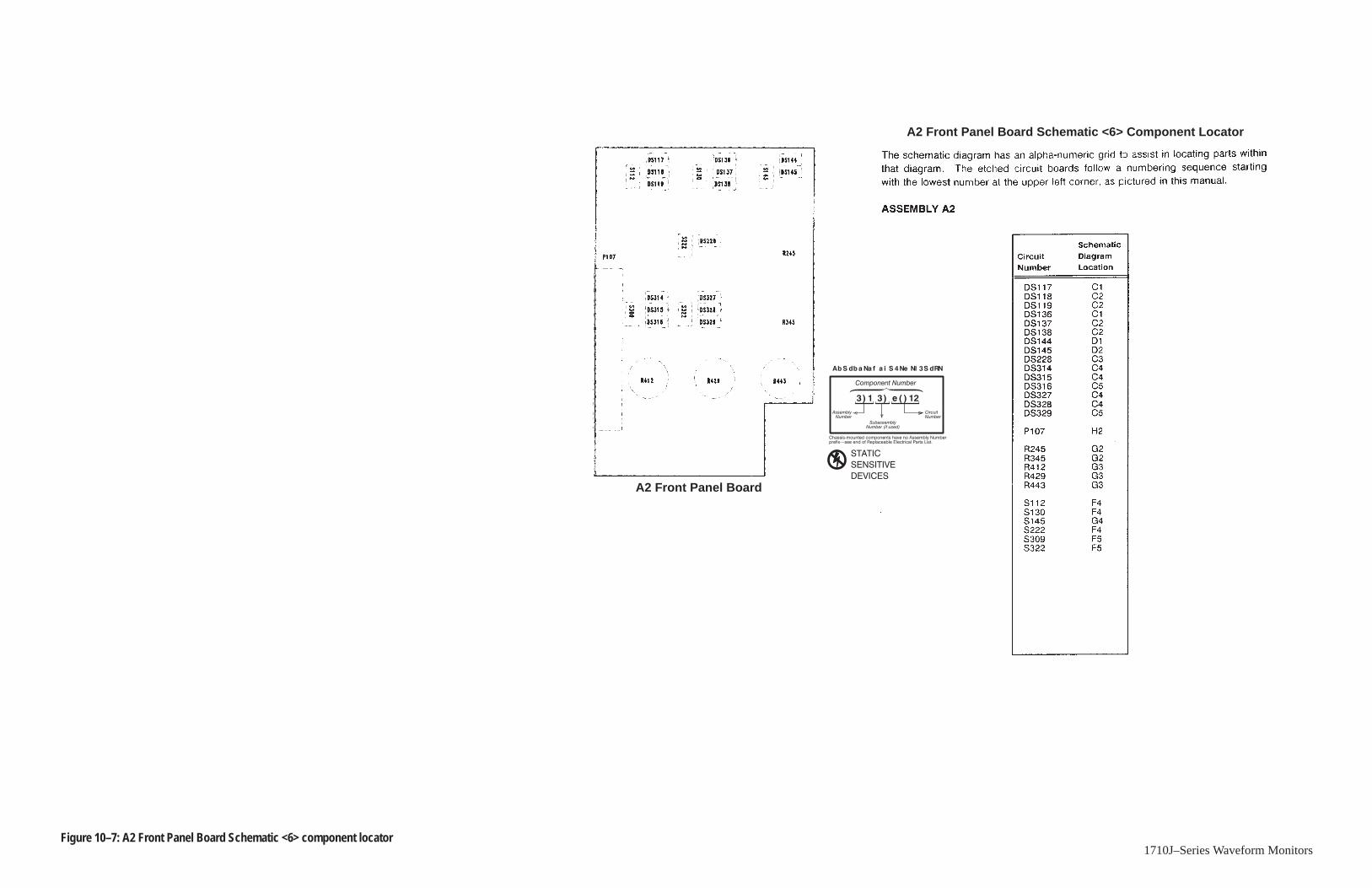
"! #
A2 Front Panel Board
A2 Front Panel Board Schematic <6> Component Locator
Figure 10–7: A2 Front Panel Board Schematic <6> component locator1710J–Series Waveform Monitors

" "
!
!
!
$
$
$
("
$ "
!
!
!! &"
!
#"
!
&
!
!
!'
"!
!
"!
"!
!
#!
!
"!
$!
$
"
$
$
#"
#"
"
!%
$
$
!
#!
"
! !
!
)!
!
$ "
("
&
!
!
$ "
#"
!
"
#"
!%
!%
! ! ("
!
)!
!
1710J WAVEFORM MONITOR
"
FRONT PANEL <6>

A1 Power Supply Board
C29 F2 F1C30 F2 F2C31 F3 F3C32 F2 F3C33 G2 F4C35 F3 G3C36 G2 G3C37 G3 G4C38 G2 G4C39 E4 G4C40 F4 H4C41 E4 I4C42 D3 I1C43 C4 J4C44 D2 I3C45 D4 I4C46 C5 I4C47 A3 J3C48 C4 J4C49 D3 J2C50 C3 J2C51 C3 K2C52 C4 J2C53 E3 I2C54 C2 M2C55 E3 H3C56 B2 M3C57 B2 N5
C58 B3 J2C59 B4 J3C60 B5 J4C61 D4 I4C62 E1 H1C63 E1 G1
CR10 F1 G2CR11 F2 G2CR12 F2 G1CR13 F3 G2CR14 E2 G3CR15 E4 G5CR16 D5 I4CR17 E2 I2CR18 D2 I2CR19 B3 K3CR20 E3 I3CR21 B2 L4CR22 B2 L4CR23 B2 L4CR24 B2 L4CR25 B3 J2CR26 F4 G4CR27 D3 J1CR29 E4 H5
DS4 D2 L2F1 B2 M4
J2 H5 B5J4 H3 F5J5 H1 F1J6 A2 M3J10 A2 N1
L1 F3 F2L2 F2 G1L3 F2 G2L4 C2 N1
Q7 D5 I4Q8 E4 I4Q9 D3 J1Q11 G3 G3
R13 F3 H4R14 F3 H4R62 D4 I4R67 F2 F4R68 F4 G5R69 G4 G5R70 G4 G4R71 F4 H4
R72 D5 H4R73 E5 H4R74 C4 J5R75 B5 J4R76 C5 I4R77 D4 I4R78 B4 J4R79 B3 J2R80 C4 J4R81 D3 J1R82 C3 J2R83 C5 J2R84 B5 J2R85 G4 G5R86 D3 J1R87 D3 K2R88 B4 J2R89 B2 M4R90 E3 I3R91 D2 K1R92 D2 K1R93 D2 L2R94 D2 L2R95 B4 J3R96 A4 K3R97 A3 J3R98 F4 G5
R99 G4 H5R101 C3 K2R102 C2 M1
RV1 D2 I3
T2 E4 H5T3 E2 G3
TP1 F5 F4TP2 E5 K4
U3A C4 J3U3B B3 J3U4A D4 I5U4B C4 I5U5 C3 J2
VR1 F4 H4VR3 F3 H4VR4 F4 H4
W1 G3 E4W2 G3 E4W3 G2 E4W4 G2 E5
The schematic diagram has an alphanumeric grid to assistin locating parts within that diagram.
Assembly A1. Partial Assembly A1 also shown on Diagram 8.
VR5VR6
"! #
A1 Power Supply Board Schematic <7>Component Locator
Figure 10–8: A1 Power Supply Board Schematic <7> component locator1710J–Series Waveform Monitors

!
)
&
)
)
+#!
+#!
*
*
*
)
)
)
&
&
&
(
&
&*
&
)
&
&
&
&
&
'
)
& &
&&
)
)
&
) !
&
*
&
&
)
#!$
*
'"
&((
&
*
#)(
"
))
*
)
)
)
&
$
&
)
)
)
)
*
&
+#!
+#!
)
*
*
)
*
*
*
*
.,'
#)'
*
%
*& &
&
&
&
%
&
&
&
&
&
&
*
&
)
$
,
&,
%
%
)
)
&
&
*
&
&
) !
&
)
)
* *
)
$
&
*
*
*
*
"
,
&,
%
%
)
&
)
)
*
(
%
& $
&
&
$
&
*
& &
&
*&
*&
*
&
&
*
&
&
*
($
&
&
($
*
* %
&
)&
*
&
&
)
)(#" &)(&-(#(
!#)"("
LINE RECTIFIERAND FILTER
(#('# (#"#)"&-'($#+& "$#("( "&%)&'"'# (#"(&"'#&!&(#'&*
#)"&-'# (#"
CLAMP
"#("'(
OUTPUT FILTERS
#$&
)$&#" -
)'+(
*
&&$"
OUTPUT UVSHUTDOWN PULSE
WIDTHMODULATOR
SWITCHERMOSFET SNUBBER
"#("'(
"
#""('
!"#&
(#
ERROR
*
#)"&-'# (#"
%"
"
(&"'#&!&
&*&
"
"
"
' AMPLIFIER
* *)'($#+&
&#"($"
#$"#"
'
"'#!!#"'#"&-&#)"'''&#)"$
((#&
1710J WAVEFORM MONITOR LOW VOLTS POWER SUPPLY <7>
"#( '$&(' '(#&& &* )'"'& ")!&&"' $&(#$#+&')$$ -

A10 CRT Socket Board (Back of Board)A10 CRT Socket Board (Front of Board)
C1 C4 A4C2 D3 D1C3 D3 A2C4 D3 A2C5 D4 B3C6 C4 B4C7 F3 B1C8 C3 B2C9 E2 B2C10 C5 B4C11 E2 B1C12 D2 C4C13 D2 C4C14 D2 C4C15 F2 C4C16 C2 C3C17 F2 D4C18 F3 E1C19 C1 D4C20 C2 D4C21 C1 D4C22 B2 E2C23 B2 E3C24 D1 E4C25 A3 E2C27 B1 E3
C28 B1 E3C34 D1 F4C65 B2 E4C66 A2 E2
CR1 E2 B1CR2 D4 B3CR3 E2 B1CR4 C2 B2CR5 D2 C3CR6 E2 C3CR7 C2 D4CR8 C2 D4CR9 C1 E4CR30 A2 E2CR31 A2 E2
DS1 E2 B2DS2 E2 B2DS3 E3 B1
FIL1 C3 C1FIL2 C3 C1
J1 F3 B1J3 F2 D1
J11 F4 A2
Q1 E5 B3Q2 E5 A3Q3 D4 B4Q4 D4 B4Q5 C4 B4Q6 B2 E1Q10 A2 E2
R1 E3 A1R2 E4 A2R3 E4 A2R4 E4 A3R5 E5 A3R7 B4 A4R8 B4 A4R11 F4 A2R12 D3 C1R20 C4 A4R21 C5 A4R22 D5 A4R23 B4 A4R24 D5 A4R25 B4 A4
R26 E5 A3R27 E5 A4R28 E5 A4R29 D2 B1R30 D2 A2R31 D4 B3R32 E5 B3R33 C4 B4R34 C4 B4R35 D4 B3R36 D4 B3R37 C5 B4R38 E2 B1R39 E2 B1R40 D2 B2R41 D4 B3R42 E3 C1R43 E2 B3R44 D2 B3R45 F2 C4R46 E3 C1R47 D2 C3R48 C2 C4R49 F2 C4R50 F2 E1
R51 F3 E1R52 F2 E1R53 F2 E1R54 F2 E1R55 D2 D4R56 F3 E1R57 B2 E1R58 D2 E4R59 B1 E2R60 C1 E3R61 D1 E4R63 A2 E2R64 C2 E2R65 B1 E3R66 B1 E3R103 A2 E2
T1 B2 C4
U1 D1 C1U2 B1 F4
VR2 A2 E2VR5 F8 C2
A1 Power Supply Board Schematic <8> Component Locator
The schematic diagram has an alphanumeric grid to assist in locating parts within that diagram.
Assembly A1. Partial Assembly A1 also shown on Diagram 7.
"! #
Figure 10–9: A1 Power Supply Board Schematic <8> component locator1710J–Series Waveform Monitors
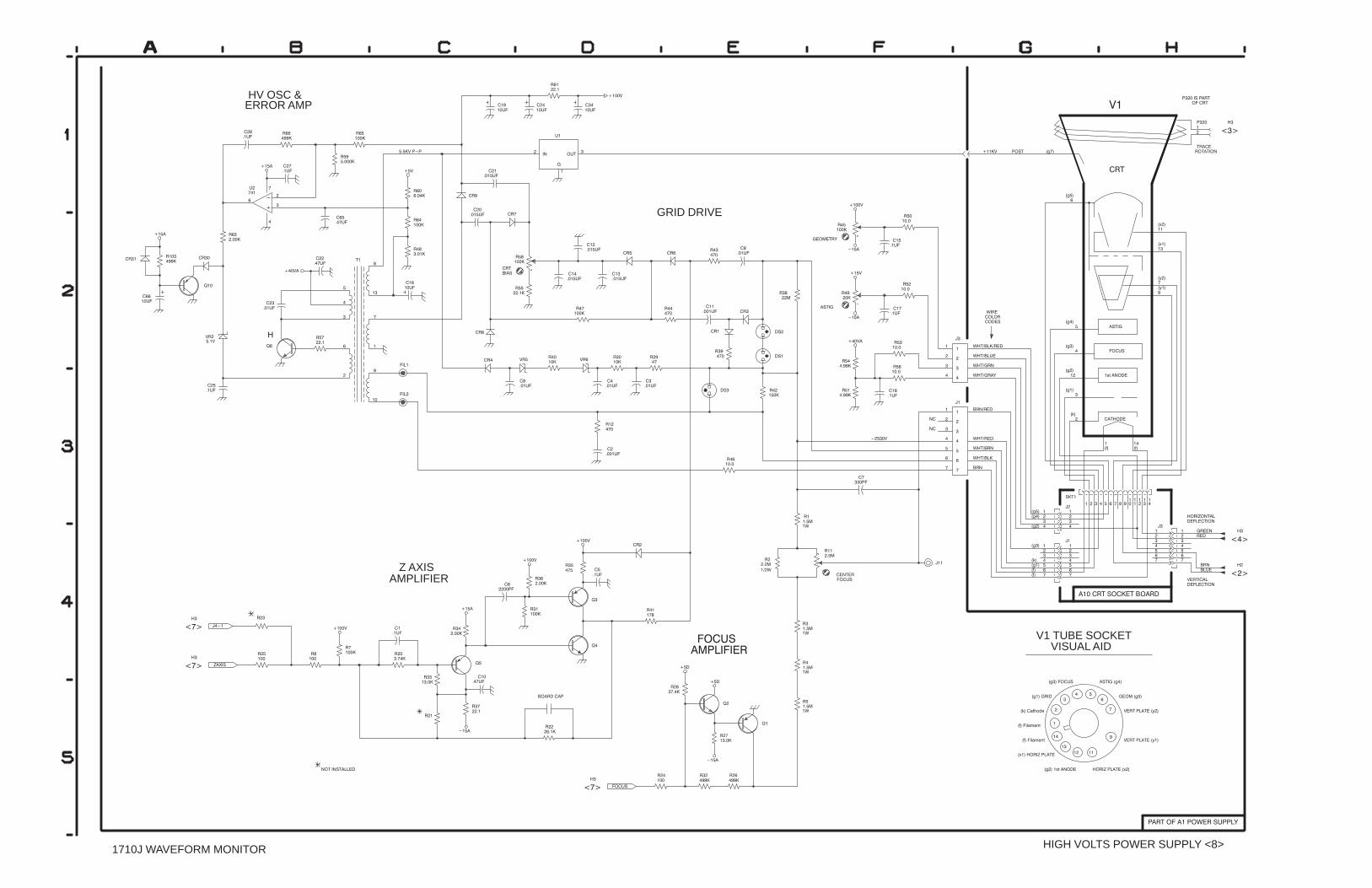
$
(
'
'
'
'
'
'
$
$
$
'
(
$
$
$
'
$
'
!'&
'
$
$
(
$
'
'
$
(
$
$
'
'$
$
$ %
$
$
$
$
'
'
'
$
$
$
$
'
$
$
'
&
'
(
$
'
$
#
($
#
$
'
$
'
'
'
'
$$
$
($ ($
$
%
%$ $
$
'
(
$
$
$
"
$
$
$
$
(
($
$
,*%
$
$
$
$
$
'
(
$
$
#
$
'
"
'
#
#
$
$
$
$
$
$
#
#
$
$
$
!'%
$
$
$
"%"$&!$&(
HV OSC &ERROR AMP
(""
GRID DRIVE
"!%&(
$&
1
1
"
$!&&! &$
;
;
<
<
!!$!%
)$
%&1
!&$+
%&
$&%
(
(
)&'
)&$+
$ $
)&$
)&$
)&$
)&$
9: !
!'%
&!
1
1
1
4
0 0
$ $
$ '
!$,! &&!
)&
$
014
1
1
11
%&
)
)Z AXIS
AMPLIFIER
!'%"$
)
)
&$!'%
V1 TUBE SOCKETVISUAL AID
%&11!'%
0
$&%!&!$
&! ($&
!1
($&"&<
($&"&<
19: !
;!$,"&
035-6/7:
035-6/7:
4-:28./
1$
!$,"&;
)
!$"
!& %&
1710J WAVEFORM MONITOR HIGH VOLTS POWER SUPPLY <8>
"$&!"!)$%'""+


Replaceable Mechanical Parts


1710J-Series Waveform Monitors 11–1
Replaceable Mechanical Parts
This section contains a list of the replaceable mechanical components for the1710J-Series Waveform Monitors. Use this list to identify and order replacementparts.
Parts Ordering InformationReplacement parts are available through your local Tektronix field office orrepresentative.
Changes to Tektronix products are sometimes made to accommodate improvedcomponents as they become available and to give you the benefit of the latestimprovements. Therefore, when ordering parts, it is important to include thefollowing information in your order.
Part number
Instrument type or model number
Instrument serial number
Instrument modification number, if applicable
If you order a part that has been replaced with a different or improved part, yourlocal Tektronix field office or representative will contact you concerning anychange in part number.
Change information, if any, is located at the rear of this manual.
Using the Replaceable Mechanical Parts ListThe tabular information in the Replaceable Mechanical Parts List is arranged forquick retrieval. Understanding the structure and features of the list will help youfind all of the information you need for ordering replacement parts. Thefollowing table describes the content of each column in the parts list.
Replaceable Mechanical Parts
11–2 1710J-Series Waveform Monitors
Parts List Column Descriptions
Column Column Name Description
1 Figure & Index Number Items in this section are referenced by figure and index numbers to the exploded viewillustrations that follow.
2 Tektronix Part Number Use this part number when ordering replacement parts from Tektronix.
3 and 4 Serial Number Column three indicates the serial number at which the part was first effective. Column fourindicates the serial number at which the part was discontinued. No entries indicates the part isgood for all serial numbers.
5 Qty This indicates the quantity of parts used.
6 Name & Description An item name is separated from the description by a colon (:). Because of space limitations, anitem name may sometimes appear as incomplete. Use the U.S. Federal Catalog handbookH6-1 for further item name identification.
7 Mfr. Code This indicates the code of the actual manufacturer of the part.
8 Mfr. Part Number This indicates the actual manufacturer’s or vendor’s part number.
Abbreviations conform to American National Standard ANSI Y1.1–1972.
Chassis-mounted parts and cable assemblies are located at the end of theReplaceable Electrical Parts List.
The table titled Manufacturers Cross Index shows codes, names, and addressesof manufacturers or vendors of components listed in the parts list.
Abbreviations
Chassis Parts
Mfr. Code to ManufacturerCross Index

Replaceable Mechanical Parts
1710J-Series Waveform Monitors 11–3
Manufacturers Cross Index
Mfr.Code Manufacturer Address City, State, Zip Code
0JR05 TRIQUEST PRECISION PLASTICS 3000 COLUMBIA HOUSE BLVDPO BOX 66008
VANCOUVER, WA 98666–6008
0KB01 STAUFFER SUPPLY CO 810 SE SHERMAN PORTLAND, OR 97214–4657
0KB05 NORTH STAR NAMEPLATE INC 5750 NE MOORE COURT HILLSBORO, OR 97124–6474
0KBZ5 Q & D PLASTICS INC 1812 – 16TH AVENUEPO BOX 487
FOREST GROVE, OR 97116–0487
06915 RICHCO 5825 N TRIPP AVEP.O. BOX 804238
CHICAGO, IL 60646
22670 GM NAMEPLATE INCORPORATED 2040 15TH AVE WEST SEATTLE, WA 981192783
24931 BERG ELECTRONICS INC BERG ELECTRONICS RF/COAXIAL DIV2100 EARLYWOOD DRPO BOX 547
FRANKLIN, IN 46131
2K262 BOYD CORPORATION 6136 NE 87TH AVENUE PORTLAND, OR 97220
31918 ITT SWITCH PRODUCTS 8081 WALLACE RD EDEN PRAIRIE, MN 55344–8798
34785 DEK INC. 3480 SWENSEN AVE. ST. CHARLES, IL 60174–3450
3L462 QUALITY PLASTICS DIV OF MOLL PLASTICRAFTERS2101 CRESTVIEW DR.
NEWBERG, OR 97132
55335 JKL COMPONENTS 13343 PAXTON ST PACOIMA, CA 91331
55566 RAF ELECTRONIC HARDWARE INC 95 SILVERMINE ROAD SEYMOUR, CT 06483
56501 THOMAS & BETTS CORPORATION 1555 LINFIELD RD MEMPHIS, TN 38119
5F520 PANEL COMPONENTS CORP PO BOX 115 OSKALOOSA, IA 52577–0115
71400 BUSSMANN DIVISION COOPER INDUSTRIES INCPO BOX 14460
ST LOUIS, MO 63178
73743 FISCHER SPECIAL MFG CO 111 INDUSTRIAL RDPO BOX 76500
COLD SPRINGS, KY 41076
7X318 KASO PLASTICS INC 11013 A NE 39TH VANCOUVER, WA 98662
80009 TEKTRONIX INC 14150 SW KARL BRAUN DRPO BOX 500
BEAVERTON, OR 97077–0001
80126 PACIFIC ELECTRICORD CO 747 WEST REDONDO BEACHPO BOX 10
GARDENA, CA 90247–4203
85471 BOYD CORPORATION 13885 RAMONA AVE CHINO, CA 91710
85480 BRADY USA NAMEPLATE DIVISIONP O BOX 571346 ELIZABETH BRADY RD
HILLSBOROUGH, NC 27278
93907 CAMCAR DIV OF TEXTRON INC ATTN: ALICIA SANFORD516 18TH AVE
ROCKFORD, IL 611045181
9M860 ESAM INC PO BOX 376 GRANTS PASS, OR 97526
TK1547 MOORE ELECTRONICS INC 19500 SW 90TH CTPO BOX 1030
TUALATIN, OR 97062
TK1617 CRAFT FACTORY PLASTICS 17145 SW ALEXANDER ALOHA, OR 97007
TK1665 PORTLAND DIE & STAMPING CO INC 4805 SE 26TH AVE PORTLAND, OR 97202
TK2364 CAPSTONE ELECTRONICS 9500 SW NIMBUS AVEBUILDING E
BEAVERTON, OR 97008–7163

Replaceable Mechanical Parts
11–4 1710J-Series Waveform Monitors
Manufacturers Cross Index (Cont.)
Mfr.Code City, State, Zip CodeAddressManufacturerTK2469 UNITREK CORPORATION 3000 LEWIS & CLARK HWY
SUITE 2VANCOUVER, WA 98661
TK2541 AMERICOR ELECTRONICS LTD UNIT–H2682 W COYLE AVE
ELK GROVE VILLAGE, IL 60007
Replaceable Mechanical Parts List
Fig. &IndexNumber
Tektronix PartNumber
Serial No.Effective
Serial No.Discont’d Qty Name & Description
Mfr.Code Mfr. Part Number
11–1–1 426–2102–00 1 FRAME,CRT:BEZEL 3L462 ORDER BY DESCR
–2 378–0258–00 1 FLTR,CONTRASTIN:GRAY,POLYCARBONATE 80009 378–0258–00
–3 211–0721–00 10 SCREW,MACHINE:6–32 X 0.375,PNH,STL,CDPL,T–15 TORX 0KB01 ORDER BY DESCR
–4 426–2101–01 1 FRAME SECT,CAB:FRONT 3L462 ORDER BY DESCR
–5 175–9872–01 1 CA ASSY,SP,ELEC:2,18 AWG,2.5 L,0–N TK2364 175–9872–01
–6 174–2648–00 1 CA ASSY,SP:RIBBON,POWER SWITCH TK2469 174–2648–00
–7 211–0100–00 2 SCREW,MACHINE:2–56 X 0.750,PNH,STL CD PL,POZ 0KB01 ORDER BY DESCR
–8 260–2465–00 1 SWITCH,PUSH:0.4A,125VAC,BTN W/YEL INDICATOR 31918 (602844)
–9 210–0405–00 2 NUT,PLAIN,HEX:2–56 X 0.188,BRS CD PL 73743 12157–50
–10 ––––––––––– 1 CIRCUIT BD ASSY:FRONT PNL(SEE A2 REPL)
–11 366–0616–00 6 PUSH BUTTON:0.585 X 0.3 X 0.150 7X318 ORDER BY DESCR
–12 333–3892–02 1 PANEL,FRONT:MAIN(1710J ONLY)
80009 333–3892–02
333–3893–02 1 PANEL,FRONT:MAIN(1711J ONLY)
80009 333–3893–02
–13 366–1701–01 B041533 5 KNOB:GY,0.127 ID X 0.392 OD X 0.4 H (1710J ONLY)
80009 366–1701–01
–13 366–0807–00 B041534 5 KNOB:GRAY,0.127 ID X 0.392 OD X 0.525 H,NON–HEATSTAMPED,366–0807–00 (1710J ONLY)
0JR05 366–0807–00
–13 366–1701–01 B040483 5 KNOB:GY,0.127 ID X 0.392 OD X 0.4 H (1711J ONLY)
80009 366–1701–01
–13 366–0807–00 B040484 5 KNOB:GRAY,0.127 ID X 0.392 OD X 0.525 H,NON–HEATSTAMPED,366–0807–00 (1711J ONLY)
0JR05 366–0807–00
–14 333–3894–00 1 PANEL,FRONT:SMALL,1710J/11J 0KB05 333–3894–00
–15 211–0690–02 2 SCR,MACH:6–32 X 0.875,PNH,SST BLKOXD,TORX & SLOT 93907 B20–70430
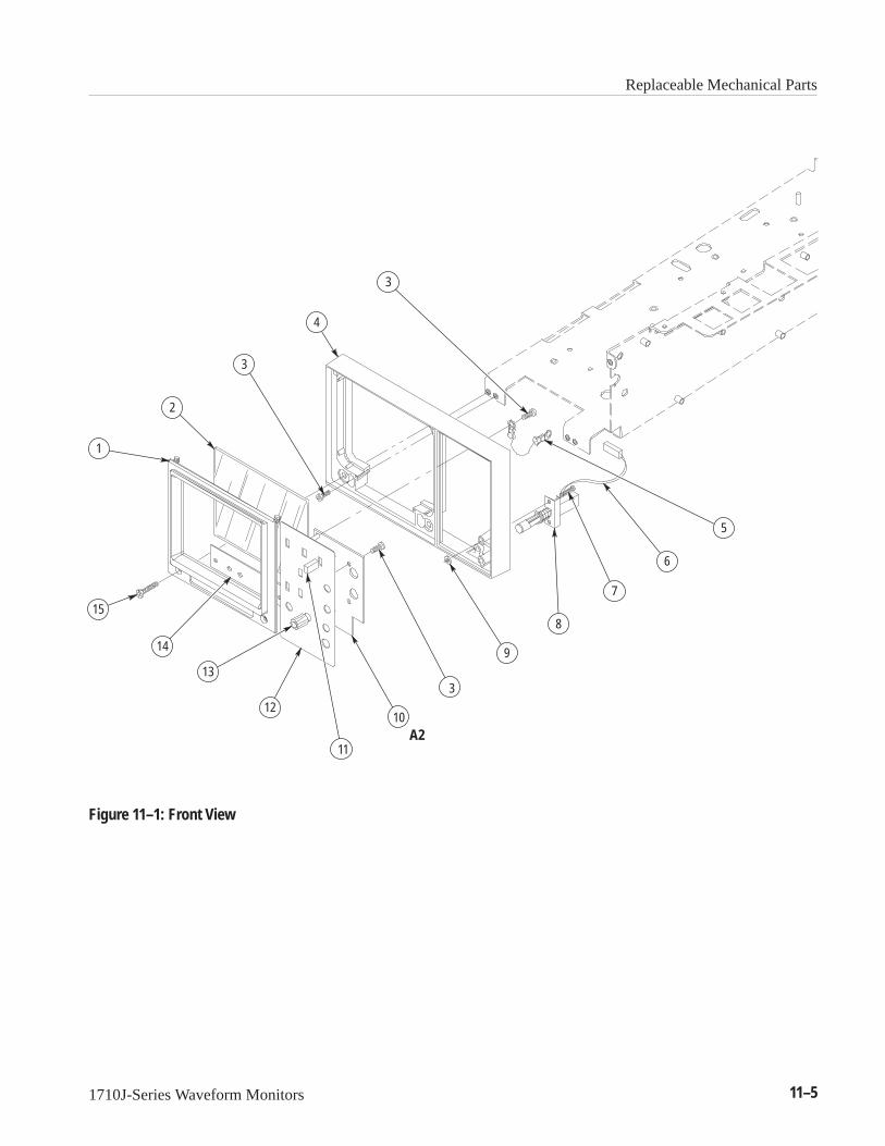
Replaceable Mechanical Parts
1710J-Series Waveform Monitors 11–5
1
2
3
4
3
5
6
7
8
9
3
10
11
12
13
14
A2
15
Figure 11–1: Front View

Replaceable Mechanical Parts
11–6 1710J-Series Waveform Monitors
Fig. &IndexNumber
Tektronix PartNumber
Serial No.Effective
Serial No.Discont’d Qty Name & Description
Mfr.Code Mfr. Part Number
11–2–1 ––––––––––– 1 ELECTRON,TUBE:CRT,FINISHED(SEE V1 REPL)
–2 386–4443–00 B041270 1 SUPPORT,SHIELD:CRT,FRONT,PLASTIC 80009 386–4443–00
386–6911–00 B041271 4 SUPPORT, SHIELD:CRT SHIELD SUPPORT,PLASTIC,1740A 7X318 1365
–3 334–1379–00 1 MARKER,IDENT:MKD HI VACUUM 22670 ORDER BY DESCR
–4 337–4064–00 B041270 1 SHIELD,ELEC:MU–METAL CRT SHIELD,SAF CONTROLLED 80009 337–4064–00
337–4087–01 B041271 1 SHIELD,ELEC:MU–METAL CRT SHIELD,SAF CONTROLLED 80009 337–4087–01
–5 346–0133–00 1 STRAP,TIEDOWN,E:14.0 X 0.091,NYLON 56501 TY234M EURODIRECT PURCH
–6 348–1464–00 1 MANCHET:CRT,END RUBBER MANCHET,31.5MM THK X63MM OD,50.5 ID
80009 348–1464–00
–7 210–0457–00 2 NUT,PL,ASSEM WA:6–32 X 0.312,STL CD PL 0KB01 ORDER BY DESCR
–8 407–4395–00 1 BRACKET,CRT:BACK,0.062,AL 80009 407–4395–00
–9 ––––––––––– 1 CIRCUIT BD ASSY:CRT SOCKET(SEE A10 REPL)
–10 174–3511–01 1 CA ASSY,SP:DISCRETE,CPD,4,24 AWG, 8.0L,1X7,0.1CTR &2, 24 AWG, 8.5L X STRAIN RELIEF PCB,
80009 174–3511–01
*ATTACHED PARTS*
344–0111–00 2 INSUL,SPREADER:DEFL LEADS,POLYPROPYLENE TK1617 NA343–0298–00 1 STRAP,RETAINING:0.25 DIA CABLE 85480 HCNY–250NA
*END ATTACHED PARTS*
–11 179–2997–01 1 WIRE HARNESS:DESCRETE,CRT ASSY 5,24AGW,5,26 AGW 9M860 179–2997–01
–12 426–2103–07 1 FRAME,CHASSIS:CHASSIS FRAME,ALUM 80009 426–2103–07
–13 337–3321–00 1 SHIELD,ELEC:CKT BD 85471 337–3321–00
–14 129–1308–00 B041023 1 SPACER,POST: 6–32 X 0.75, HEX, STL, CAD PL 55566 4538–632–S–3 –15 343–0013–00 B041023 CLAMP,LOOP:0.375 ID,PLASTIC,SAFETY CONTROLLED 06915 E6 CLEAR ROUND
CABLE CLAMP
– 16 211–0720–01 B041023 1 SCREW,MACHINE:6–32 X 0.50 HEX,STL, CAD PL 0KB01 211–0720–01
–17 ––––––––––– 1 CIRCUIT BD ASSY:MAIN(SEE A3 REPL)
–18 343–0916–00 B041022 1 CLAMP,LOOP:0.5 ID,NYLON 34785 029–500
–18 211–0721–00 B041022 8 SCREW,MACHINE:6–32 X 0.375,PNH,STL,CDPL,T–15 TORX 0KB01 ORDER BY DESCR
–18 211–0721–00 B041023 7 SCREW,MACHINE:6–32 X 0.375,PNH,STL,CDPL,T–15 TORX 0KB01 ORDER BY DESCR
–19 ––––––––––– 1 CIRCUIT BD ASSY:GRATICULE LIGHT(SEE A3A1 REPL)
–20 348–0171–00 1 GROMMET,PLASTIC:BLACK,U–SHAPED,0.276 ID 0KBZ5 NA

Replaceable Mechanical Parts
1710J-Series Waveform Monitors 11–7
1
2
3
4
5
6
7
8
9
10
11
12
13
14
A10
A3
A3A1
15
16
17
18
19
20
Figure 11–2: CRT, Chassis and Main Bd

Replaceable Mechanical Parts
11–8 1710J-Series Waveform Monitors
Fig. &IndexNumber
Tektronix PartNumber
Serial No.Effective
Serial No.Discont’d Qty Name & Description
Mfr.Code Mfr. Part Number
11–3–1 174–2277–00 1 CA ASSY,SP:RIBBON,IDC,15,28AWG,20.0L TK1547 174–2277–00
–2 333–3895–01 B040152 1 PANEL,REAR:1710J/1711J 80009 333–3895–01
–2 333–3895–02 B040153 1 PANEL,REAR:REAR PANEL,ALUM,1710J/1711J, 80009 333–3895–02
–3 211–0720–01 2 SCREW,MACH:6–32 X 0.50,PNH,STL,TORX T–15 WITH SLOT 0KB01 211–0720–01
–4 214–3903–01 2 SCREW,JACK:4–40 X 0.312 EXT THD,4–40 INT THD 0KB01 214–3903–01
–5 210–0255–00 1 TERMINAL,LUG:0.391 ID,LOCKING,BRS CD PL TK1665 ORDER BY DESCR
–6 211–0721–00 10 SCREW,MACHINE:6–32 X 0.375,PNH,STL,CDPL,T–15 TORX 0KB01 ORDER BY DESCR
–7 131–0106–02 6 CONN,RF JACK:BNC,50 OHM,FEMALE 24931 28JR178–1
–8 211–0014–00 2 SCREW,MACHINE:4–40 X 0.5,PNH,STL CD PL,POZ 93907 ORDER BY DESCR
–9 131–3573–00 1 CONN,PLUG,ELEC:MALE,W/LOCKING ADAPTER 80126 B–0779
–10 337–3796–01 1 SHIELD,ELEC:0.032 BRASS,C26000,0.5 HARD 80009 337379601
–11 337–3931–00 1 SHIELD,ELEC:ALUMINUM 80009 337393100
–12 ––––––––––– 1 CIRCUIT BD ASSY:MAIN(SEE A3 REPL)
–13 337–3257–00 2 SHIELD,CKT BD:LV PWR SUPPLY 2K262 ORDER BY DESCR
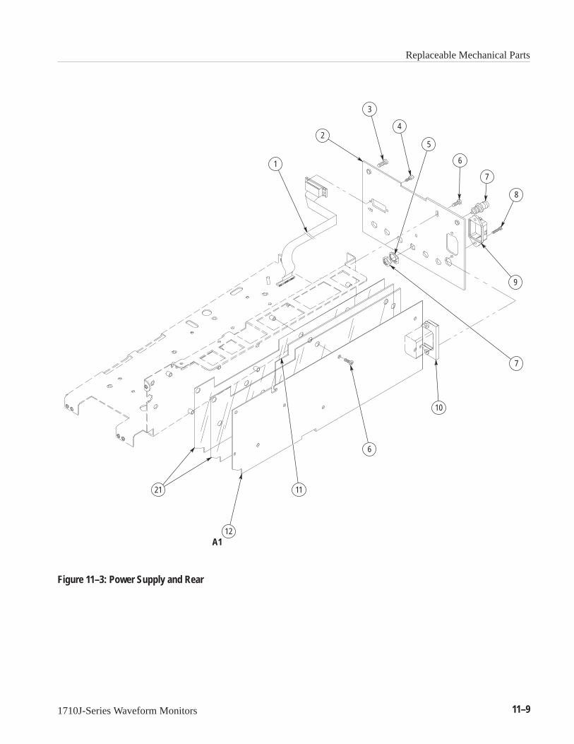
Replaceable Mechanical Parts
1710J-Series Waveform Monitors 11–9
1
2
3
4
5
6
7
8
9
7
10
6
11
12
21
A1
Figure 11–3: Power Supply and Rear

Replaceable Mechanical Parts
11–10 1710J-Series Waveform Monitors
Fig. &IndexNumber
Tektronix PartNumber
Serial No.Effective
Serial No.Discont’d Qty Name & Description
Mfr.Code Mfr. Part Number
STANDARD ACCESSORIES
070–9673–03 1 MANUAL,TECH:INSTRUCTION,WAVEFORMMONITOR,1710J/1711J
80009 070–9673–03
011–0163–00 2 TERM,COAX:BNC,TERMINATION SINGLR ENDED,75 OHM 4Y264 BCP–TA
159–0021–00 1 FUSE,CARTRIDGE:3AG,2A,250V,FAST BLOW 71400 AGC–2
150–0168–00 4 LAMP,INCAND:14V,0.08A,WEDGE BASE,T1.75 FOR SKT MT 55335 73W
378–0335–00 4 FILTER,AIR:1.6 X 1.6,30PPI,0.188 THK 2K262 ORDER BY DESCR
11–4–1 161–0216–00 1 CABLE ASSY,PWR:3,18 AWG,2.5M L,BLACK 80126 C7120–25M–BL
OPTIONAL ACCESSORIES
–2 161–0215–00 1 CABLE ASSY,PWR:3,0.75MU,2.5MM L,GREY(EUROPEAN OPTION A1 ONLY)
80126 0–5335–008–GY
–3 161–0066–10 1 CA ASSY,PWR:3,1.0 MM SQ,250V/10A,2.5 METER(UNITED KINGDOM OPTION A2 ONLY)
TK2541 ORDER BY DESCR
–4 161–0066–11 1 CA ASSY,PWR:3,1.0MM SQ,250V/10A,2.5 METER(AUSTRALIAN OPTION A3 ONLY)
80126 ORDER BY DESCR
–5 161–0066–12 1 CA ASSY,PWR:3,18 AWG,250V/10A,98 INCH(NORTH AMERICAN OPTION A4 ONLY)
S3109 ORDER BY DESCR
–6 161–0154–00 1 CA ASSY,PWR:3,1.0MM SQ,250V/10A,2.5 METER(SWISS OPTION A5 ONLY)
5F520 86515030
016–0475–00 1 VIEWING HOOD:1740 80009 016–0475–00
200–3897–01 1 COVER,FRONT:1700F02,HOT STAMPED 80009 200–3897–01
––––––––––– 1 CAMERA,SCOPE:C9(OPTION 20 ONLY)
FIELD UPGRADES
––––––––––– 1 PLAIN CASE ASSY:1700F00
––––––––––– 1 PTD CASE ASSY:1700F02
––––––––––– 1 RACK ADAPTER:1700F05
––––––––––– 1 FILLER PANEL:1700F06
––––––––––– 1 DRAWER,UTILITY:1700F07

Replaceable Mechanical Parts
1710J-Series Waveform Monitors 11–11
12
3
45
6
Figure 11–4: Accessories

Replaceable Mechanical Parts
11–12 1710J-Series Waveform Monitors

1710J-Series Waveform Monitors Glossary–1
Glossary
AccuracyThe closeness of the indicated value to the true value.
Black LevelThe level of the picture signal that corresponds to the maximum black peaks.
Blanking LevelThe level of the picture signal that separates the picture information from thesynchronizing information. Also see Setup.
ChrominanceThe property of light that produces a sensation of color in the human eyeapart from any variation in luminance that may be present.
Chrominance FilterA specially designed filter that passes the chrominance portion of the colorsignal while reducing the amplitude of other frequencies.
ClampA circuit that adds a fixed bias level to a particular portion of the televisionwaveform. Also see DC Restorer.
Color Bar SignalA test signal typically containing eight basic colors (white, yellow, cyan,green, magenta, red, blue, and black) that is used to check chrominancefunctions of the color television system.
Color BurstA sample of chrominance subcarrier frequency that establishes a referencefor demodulating the chrominance signal.
Composite VideoA signal containing vertical (field), horizontal (line) synchronizing signals,color synchronizing (burst) signal, and the picture luminance and chromi-nance information.
DC RestorerA circuit used in waveform monitors and picture monitors to clamp onepoint of the waveform to a fixed DC level.
Differential GainThe difference in output amplitude, expressed in percent of dB, of a smallhigh frequency sine wave signal at two stated levels of a low frequencysignal on which it is superimposed.

Glossary
Glossary–2 1710J-Series Waveform Monitors
Differential PhaseThe difference in output phase of a small high frequency sine wave signal attwo stated levels of a low frequency signal on which it is superimposed.
Field TiltThe distortion of the television waveform where the amplitude of the signaldisplays a sloping distortion over the duration of at least one full field ofvideo.
FlatThe non-filtered display of the television signal.
K-FactorA method of determining the visual impairment of the television signal.
Low-Pass FilterA filter having a single transmission band extending from zero frequency upto a specified cutoff frequency.
LuminanceThe amount of light intensity, which is perceived by the eye as brightness.
Luminance FilterA low-pass filter whose upper frequency limit is set by the luminance signalfrequency of the television system.
NTSCNational Television Systems Committee. The organization that developedthe television standard currently in use in the United States, Canada, andJapan. Now generally used to refer to that standard.
PALPhase Alternate Line. Refers to one of the television systems used in Europeand many other parts of the world. The phase of one of the color differencesignals alternates from line to line to help cancel out phase errors.
Pulse-to-Bar RatioA test method to measure short time distortions of the television signal.
Return LossThe ratio, in dB, of the power incident upon a discontinuity and the powerreflected from the discontinuity.
RGB/YRGBRed, green, and blue. The three primary colors used in color television’sadditive color reproduction system. These are the three color componentsgenerated by the camera and used by the receiver to reproduce a picture.YRGB is the color components plus the luminance component (Y).

Glossary
1710J-Series Waveform Monitors Glossary–3
Setup Level (NTSC)The difference between the blanking level and the reference black level.Normally 7.5% (7.5 IRE) is the amount of setup employed.
Staircase SignalA video test signal containing several steps of equal amplitude at increasingluminance levels. The staircase signal is usually amplitude modulated by asubcarrier frequency and is useful in checking amplitude and phaselinearities in the video system.
Sync, Horizontal (Line Rate)A pulse signal occurring at the line rate of the television scanning systemthat is used to stop and start horizontal scanning.
Sync, Vertical (Field Rate)A pulse signal occurring at the field rate of the television scanning systemthat is used to stop and start vertical scanning. This signal consists of aserrated block pulse surrounded by horizontal equalizing pulses, which occurat twice the horizontal sync rate.
Sync StripperA circuit whose function is to remove the synchronizing components fromthe composite television signal and deliver the synchronizing pulses to thedisplay circuits.
Vertical IntervalThe period of time during which the display device performs vertical retrace.This interval contains the vertical synchronizing pulse and the horizontalequalizing pulses.
Waveform MonitorA specialized oscilloscope that is triggered by either horizontal or verticalsync pulses to display a time versus amplitude display of television signalelements.
White LevelThe picture signal level corresponding to a specified limit for the whitepeaks.

Glossary
Glossary–4 1710J-Series Waveform Monitors

1710J-Series Waveform Monitors Index–1
IndexNumbers75 ohm Termination, 1–4
AAC Power Plug, 2–4Accessories, 1–2
Optional Accessories, 1–3Standard Accessories, 1–2
Accuracy, Glossary–1Adjustment Procedure, 7–1
+5 V Adjust, 7–40.2 microsecond Sweep Calibration, 7–72-line and 1 microsecond Sweep Calibration, 7–7Calibrator Signal Amplitude, 7–10Chroma Filter, 7–15CRT Bias, 7–5Dual Filter Switching, 7–8Dual Input DC Level, 7–11Geometry, Focus, and Astigmatism, 7–5Input A Compensation and Flat Response, 7–11Input B Compensation, 7–13Low Pass Filter, 7–14Magnifier Registration, 7–9Main Circuit Board Regulated Power Supplies, 7–6Preliminary Setup, 7–3Procedure, 7–3Required Test Equipment, 7–1
Parade Display Test Connector, 7–3RGB Compensation, 7–9RGB Offset, 7–9Static Discharge Precautions, 7–1Trace Rotation, 7–6Vertical Amplifier Output Bias, 7–10X5 Gain HF Response, 7–14X5 Magnifier Registration, 7–11
Analyzing a Video Signal, 3–5The Creative Part of the Video Signal, 3–7The Test Signal in the Video Signal, 3–5
BBlock Diagram
CRT, Unblanking, and High Voltage, 5–3Horizontal, 5–2Vertical, 5–2
CCabinet Installation, 1–7Cabinets, 1–6CH A - CH B, 2–2CH A Input Connector, 2–5CH B Input Connector, 2–5Cleaning, 8–7
CRT, 8–7Exterior, 8–7Interior, 8–7
Cleaning & Inspection, Cleaning, 8–7CRT, 8–7Exterior, 8–7Interior, 8–7
Cleaning and Inspection, 8–7Performance Verification and Readjustment, 8–8Visual Inspection, 8–8
Connecting to the Program Line, 1–475 ohm Termination, 1–4
Custom Installation, 1–10
EElectrical Installation, 1–3
Mains Frequency, 1–4Power Source, 1–3Voltage Ranges, 1–4
External Reference Connector, 2–4
FFilter, 2–2Focus Control, 2–3Front Panel Controls and Indicators, 2–1
CH A - CH B, 2–2Filter, 2–2Focus Control, 2–3Gain, 2–2Horizontal Position, 2–3Installation Control, 2–3On -Off Switch, 2–3Reference, 2–2Rotate Control, 2–3Scale Illumination Control, 2–3Sweep Magnifier, 2–2Sweep Rate, 2–3

Index
Index–2 1710J-Series Waveform Monitors
Vertical Calibration Adjust, 2–3Vertical Position, 2–2
Front Panel, Diagram 6Controls, 5–16Indicators and Switches, 5–16
Functional Checkout Procedure, 1–12Equipment Required, 1–12
Fuse Holder, 2–4
GGain, 2–2Getting Started, 1–1
Accessories, 1–2Optional Accessories, 1–3Standard Accessories, 1–2
Connecting to the Program Line, 1–475 ohm Termination, 1–4
Electrical Installation, 1–3Mains Frequency, 1–4Power Source, 1–3Voltage Ranges, 1–4
Functional Checkout Procedure, 1–12Equipment Required, 1–12
Installation, 1–3Packaging, 1–3
Mechanical Installation, 1–6Cabinet Installation, 1–7Cabinets, 1–6Custom Installation, 1–10Rack Adapter, 1–8
Product Description, 1–1Remote Connector, 1–4
RGB/YRGB Parade Display, 1–4Typical Description, 1–2
GraticulesHorizontal Scales for NTSC and PAL Graticules,
3–3NTSC Composite Video Graticule Vertical Scales,
3–1PAL Graticule Vertical Scales, 3–3
HHandling Static Sensitive Components, 8–2
Handling Precautions, 8–3Static Susceptibility, 8–2
High Voltage Power Supply, Diagram 8Focus Amplifier, 5–20Grid Drive Circuit, 5–20HV Osc and Error Amp, 5–19Power Supply Outputs, 5–20
Horizontal Position, 2–3Horizontal Scales for NTSC and PAL Graticules, 3–3
IInstallation, 1–3
Packaging, 1–3Installation Control, 2–3Internal Plug Jumpers, 8–3
LLow Voltage Power Supply, Diagram 7
Error Amplifier, 5–19Feedback Transformer Driver and Peak Detector,
5–19Line Rectifier and Filter, 5–17Output Filters, 5–19Output Under-Voltage Shutdown, 5–19Pulse Width Modulator, 5–18
MMagnifier, 2–2Mains Frequency, 1–4Maintenance, 8–1
Cleaning and Inspection, 8–7Cleaning, 8–7Performance Verification and Readjustment, 8–8Visual Inspection, 8–8
Handling Static Sensitive Components, 8–2, 8–3Handling Precautions, 8–3
Operating Options, 8–3Internal Plug Jumpers, 8–3
Preparation, 8–2Preventive Maintenance, 8–7Remote Connector, 8–5
Pin Assignments, 8–5RGB/YRGB Parade Display, 8–5
Removal and Replacement Instructions, 8–9Bezel Removal, 8–9CRT Removal and Replacement, 8–11Front Panel and Front Panel Circuit Board Re-
moval, 8–13Graticule Light Removal and Replacement, 8–10Removing the Main Board, 8–14Removing the Power Supply Board, 8–16Removing the Rear Panel, 8–12
Repackaging, 8–28Identification Tag, 8–28Packaging Illustration, 8–29

Index
1710J-Series Waveform Monitors Index–3
Repackaging for Shipment, 8–28Service Strategy, 8–1Setting RGB Offset, 8–6Troubleshooting, 8–17
Foldout Pages, 8–17 #)312,$-2." 2(.-1 11$,!+7 -#(0"3(23,!$0(-&(0"3(2. 0#++3120 2(.-1( &0 ,1 021." 2(-&' 021
General Troubleshooting Techniques, 8–20High Voltage Power Supply, 8–26.+2 &$'$"*."31 ,/+(%($0'$"*0(#0(4$'$"*(&'.+2 &$1"(++ 2.0'$"*0$+(,(- 07'$"*18 6(1 ,/+(%($0'$"*
Low Voltage Power Supply, 8–23.-20.+(0"3(2'$"*00.0 ,/+(%($0'$"*32/32'$"*0$+(,(- 07'$"*1$"2(%($05(2"'$0'$"*
Major Assembly Interconnection, 8–19Parts Lists, 8–18$/+ "$ !+$+$"20(" + 021$/+ "$ !+$$"' -(" + 021
Specific Troubleshooting Techniques, 8–22.5$03//+70.3!+$1'..2(-&
Making a Signal Amplitude Measurement, 2–5Checking Instrument Vertical Calibration, 2–5Measure Setup Level, 2–7Measure Sync Amplitude, 2–6Measure White Level, 2–7Obtaining a Display, 2–5Signal Input, 2–5
Mechanical Installation, 1–6Cabinet Installation, 1–7Cabinets, 1–6Custom Installation, 1–10Rack Adapter, 1–8
Microcontroller, Diagram 5LED Drive, 5–16Processor, 5–13
Control Line Functions, 5–14RGB Amplifier, 5–15
NNTSC Composite Video Graticule Vertical Scales, 3–1
Making Measurements, 3–2
OOn -Off Switch, 2–3Operating Basics, 2–1
Front Panel Controls and Indicators, 2–1CH A - CH B, 2–2Filter, 2–2Focus Control, 2–3Gain, 2–2Horizontal Position, 2–3Installation Control, 2–3On -Off Switch, 2–3Reference, 2–2Rotate Control, 2–3Scale Illumination Control, 2–3Sweep Magnifier, 2–2Sweep Rate, 2–3Vertical Calibration Adjust, 2–3Vertical Position, 2–2
Making a Signal Amplitude Measurement, 2–5Rear-panel Connectors, 2–4
AC Power Plug, 2–4CH A Input Connector, 2–5CH B Input Connector, 2–5External Reference Connector, 2–4Fuse Holder, 2–4Remote Connector, 2–4
Operating Options, Internal Plug Jumpers, 8–3Optional Accessories, 1–3
PPackaging, 1–3Packaging Illustration, 8–29PAL Graticule Vertical Scales, 3–3Parade Display Test Connector, 6–2Parts Ordering Information, 11–1Performance Verification, 6–1
Parade Display Test Connector, 6–2Required Equipment List, 6–1Verification Procedure, 6–3
Check Calibrator Amplitude, 6–10Check Calibrator Frequency, 6–4Check Chrominance Filter Response, 6–15Check DC Restorer Operation, 6–10Check Flat Response, 6–12Check Low Pass Filter Response, 6–14Check Power Supply Operation, 6–4Check Return Loss, 6–15

Index
Index–4 1710J-Series Waveform Monitors
Check RGB/YRGB Parade Display, 6–8Check Sweep Calibration, 6–6Check Sweep Operation, 6–5Check Sync Separation, 6–4Check Transient Response, 6–13Check Vertical Gain, 6–9Check X5 Transient Response, 6–14Preliminary Setup, 6–3
Performance Verification and Readjustment, 8–8Power Source, 1–3Preventive Maintenance, 8–7Processor, Control Line Functions, 5–14Product Description, 1–1
RRack Adapter, 1–8Rear-panel Connectors, 2–4
AC Power Plug, 2–4CH A Input Connector, 2–5CH B Input Connector, 2–5External Reference Connector, 2–4Fuse Holder, 2–4Remote Connector, 2–4
Reference, 2–2, 3–1Analyzing a Video Signal, 3–5
The Creative Part of the Video Signal, 3–7The Test Signal in the Video Signal, 3–5
Graticules, 3–1Horizontal Scales for NTSC and PAL Graticules,
3–3NTSC Composite Video Graticule Vertical Scales,
3–1PAL Graticule Vertical Scales, 3–3
Remote Connector, 1–4, 2–4, 8–5Pin Assignments, 8–5RGB/YRGB Parade Display, 1–4, 8–5
Removal and Replacement Instructions, 8–9Bezel Removal, 8–9CRT Removal and Replacement, 8–11Front Panel and Front Panel Circuit Board Removal,
8–13Graticule Light Removal and Replacement, 8–10Removing the Main Board, 8–14Removing the Power Supply Board, 8–16Removing the Rear Panel, 8–12
Repackaging, 8–28Identification Tag, 8–28Packaging Illustration, 8–29Repackaging for Shipment, 8–28
Replaceable Electrical Parts List, 9–1Parts Ordering Information, 9–1
Replaceable Mechanical Parts, 11–1Parts Ordering Information, 11–1Using the Replaceable Mechanical Parts List, 11–1
Required Test Equipment, Parade Display TestConnector, 7–3
RGB/YRGB Parade Display, 1–4Rotate Control, 2–3
SScale Illumination Control, 2–3Setting RGB Offset, 8–6Specific Troubleshooting Techniques, 8–22
Power Supply Troubleshooting, 8–22Specifications, 4–1
Calibrator, 4–3Certifications and Compliances, 4–6CRT, 4–5DC Restorer, 4–3Environmental Characteristics, 4–6Horizontal Deflection, 4–3Input/Output and Vertical Deflection, 4–1Physical Characteristics, 4–5Power Source, 4–5RGB/YRGB, 4–4Synchronization, 4–4
Standard Accessories, 1–2Static Susceptibility, 8–2Sweep, 2–3Sweep Generators and Horiz Output, Diagram 4
Horizontal Output Amplifier, 5–13Magnifier Amplifier, 5–13Sweep Generator, 5–12
Sweep Magnifier, 2–2Sweep Rate, 2–3
TThe Creative Part of the Video Signal, 3–7The Test Signal in the Video Signal, 3–5Theory of Operation, 5–1
Block Diagram, 5–2CRT, Unblanking, and High Voltage, 5–3Horizontal, 5–2Vertical, 5–2
Front Panel, Diagram 6, 5–16Controls, 5–16Indicators and Switches, 5–16
High Voltage Power Supply, Diagram 8, 5–19Focus Amplifier, 5–20Grid Drive Circuit, 5–20
Index
1710J-Series Waveform Monitors Index–5
HV Osc and Error Amp, 5–19Power Supply Outputs, 5–20Z-Axis Amplifier, 5–21
Low Voltage Power Supply, Diagram 7, 5–17Error Amplifier, 5–19Feedback Transformer Driver and Peak Detector,
5–19Line Rectifier and Filter, 5–17Output Filters, 5–19Output Under-Voltage Shutdown, 5–19Pulse Width Modulator, 5–18
Microcontroller, Diagram 5, 5–13LED Drive, 5–16Processor, 5–13
RGB Amplifier, 5–15Overview, 5–1Sweep Generators and Horiz Output, Diagram 4,
5–12Horizontal Output Amplifier, 5–13Magnifier Amplifier, 5–13Sweep Generator, 5–12
Timing, Diagram 3, 5–9Graticule Illumination, 5–11Horizontal Sync Generator, 5–10Regulators, 5–11Timing State Machine, 5–9Trace Rotation, 5–11Vertical Sync Generator, 5–11Z-Axis Control, 5–11
Vertical Input, Diagram 1, 5–3Calibrator, 5–6Channel Switch, 5–4External Sync Input and Source Switch, 5–4Filter Selection, 5–6Input Amplifiers, 5–4Sync Stripper, 5–5
Vertical Output, Diagram 2, 5–7Gain Cell, 5–7Gain Cell Amplifier, 5–7Second DC Restorer, 5–7Switchable Gain Amplifier, 5–8Vertical Output Amplifier, 5–9
Timing, Diagram 3Graticule Illumination, 5–11Horizontal Sync Generator, 5–10Regulators, 5–11Timing State Machine, 5–9Trace Rotation, 5–11Vertical Sync Generator, 5–11Z-Axis Control, 5–11
Trace Rotation Control, 2–3Troubleshooting, 8–17
Foldout Pages, 8–17Adjustment Locations, 8–18Assembly and Circuit Numbering, 8–18Circuit Board Illustrations, 8–18Diagrams, 8–17Parts Locating Charts, 8–18
General Troubleshooting Techniques, 8–20High Voltage Power Supply, 8–26
CRT Voltage Check, 8–28Focus Amplifier Check, 8–26Grid Drive Check, 8–27High Voltage Oscillator Check, 8–27Preliminary Checks, 8–26Z-Axis Amplifier Check, 8–26
Low Voltage Power Supply, 8–23Control Circuit Check, 8–25Error Amplifier Check, 8–25Output Check, 8–24Preliminary Checks, 8–23Rectifier/Switcher Check, 8–24
Major Assembly Interconnection, 8–19Parts Lists, 8–18
Replaceable Electrical Parts, 8–18Replaceable Mechanical Parts, 8–19
Specific Troubleshooting Techniques, 8–22Power Supply Troubleshooting, 8–22
Typical Description, 1–2
VV Cal, 2–3Verification Procedure
Check Calibrator Amplitude, 6–10Check Calibrator Frequency, 6–4Check Chrominance Filter Response, 6–15Check DC Restorer Operation, 6–10Check Flat Response, 6–12Check Low Pass Filter Response, 6–14Check Power Supply Operation, 6–4Check Return Loss, 6–15Check RGB/YRGB Parade Display, 6–8Check Sweep Calibration, 6–6Check Sweep Operation, 6–5Check Sync Separation, 6–4Check Transient Response, 6–13Check Vertical Gain, 6–9Check X5 Transient Response, 6–14Preliminary Setup, 6–3
Vertical Calibration Adjust, 2–3Vertical Input, Diagram 1
Calibrator, 5–6Channel Switch, 5–4

Index
Index–6 1710J-Series Waveform Monitors
External Sync Input and Source Switch, 5–4Filter Selection, 5–6Input Amplifiers, 5–4Sync Stripper, 5–5
Vertical Output, Diagram 2Gain Cell, 5–7Gain Cell Amplifier, 5–7Second DC Restorer, 5–7
Switchable Gain Amplifier, 5–8Vertical Output Amplifier, 5–9
Vertical Position, 2–2Voltage Ranges, 1–4
WWarm-up Period, 4–1