Instruction Manual - TDK · C250-04-11C TDK-Lambda PFE500F・1000F Series INSTRUCTION MANUAL...
17
C250-04-11C TDK-Lambda PFE500F・1000F Series INSTRUCTION MANUAL PFE500F・1000F SERIES Instruction Manual BEFORE USING THE POWER SUPPLY UNIT Be sure to read this instruction manual thoroughly before using this product. Pay attention to all cautions and warnings before using this product. Incorrect usage could lead to an electrical shock, damage to the unit or a fire hazard. DANGER · Never use this product in locations where flammable gas or ignitable substances are present. WARNING · Do not make unauthorized changes to power supply unit, otherwise you might have electric shock and void your warranty. · Do not touch this unit and the internal components in operation or shortly after shut down. They might have high voltage or high temperature and as the unit dissipates its heat so the surface of the unit is hot. You might receive electric shock or burn. · When the unit is operating, keep your hands and face away from it; you might be injured by an accident. · Do not use unit under unusual condition such as emission of smoke or abnormal smell and sound etc. It might cause fire and electric shock. In such case, please contact us; do not repair by yourself, as it is dangerous for the user. · Do not drop or insert anything into unit. It might cause failure and fire. · Do not operate these units under condensation condition. It might cause fire and electric shock. CAUTION · As a component part, compliance with the standard will be based upon installation in the final application. This product must be installed in a restricted access location, accessible to authorized competent personnel only. These AC to DC converters have reinforced insulation between the input and the output. The outputs of these products are energy hazards. All models with an output greater than 28V model are considered to be non-SELV. As such, the instructions for use must refer to these energy hazardous outputs and Non-SELV outputs in that the outputs must not be accessible to the operator. The installer must also provide protection against inadvertent contact by a service engineer. · The equipment has been evaluated for use in a Pollution Degree 2 environment. · This power supply is primarily designed and manufactured to be used and enclosed in other equipment. · Confirm connections to input/output terminals and signal terminals are correct as indicated in the instruction manual. · Attach a fast acting external fuse to each module to ensure safety operation and compliance to each safety standard approval. The recommended input fuse rating within the instructions manual. The breaking capacity and voltage rating of this fuse might be subject to the end use application. · Input voltage, Output current, Output power, ambient temperature and ambient humidity should be used within specifications, otherwise the unit will be damaged. · For application equipment, which requires very high reliability (Nuclear related equipment, traffic control equipment, medical equipment, etc.), please provide fail safety function in the equipment. · Do not use the product in environment with strong electromagnetic field, corrosive gas and conductive substance. · Do not operate and store this unit at an environment where condensation occurs. In such case, waterproof treatment is necessary · Never operate the unit under over current or shorted conditions for 30 seconds or more and out of Input Voltage Range as specification. Insulation failure, smoking, burning or other damage might occur to the unit. · The output voltage of this power supply unit is considered to be a hazardous energy level (The voltage is 2V or more and the electric power is 240VA or more). Prevention from direct contact with output terminal is highly necessary. While installing or servicing this power supply unit, avoid dropping tools by mistake or direct contact with output terminal. This might cause an electrical shock. While repairing this power supply unit, the AC input power must be switched off and the input and output voltage should be level. · To maintain the SELV output for outputs less than 28VDC, under fault conditions, the output must be connected to earth in the final application. · The application circuits and their parameter are for reference only. Be sure to verify effectiveness of application circuits and their parameters before finalizing circuit design. · Do not inject abnormal voltage to output terminal and signal terminal from the outside. The injection of reverse voltage or over voltage exceeding nominal output voltage to output terminals might cause damage to internal components. · This information in this document is subject to change without prior notice. For actual design-in, please refer to the latest publications of data sheet, etc., for the most up-to date specifications of the unit. · Design the board of an application circuit implementing this product in consideration of components layout, pattern layout and pattern width. · No part of this document might be copied or reproduced in any form without prior written consent of Densei-Lambda. Note : CE MARKING CE Marking, when applied to a product covered by this handbook, indicates compliance with the low voltage directive.
Transcript of Instruction Manual - TDK · C250-04-11C TDK-Lambda PFE500F・1000F Series INSTRUCTION MANUAL...

C250-04-11C
TDK-Lambda PFE500F・1000F Series INSTRUCTION MANUAL
PFE500F・1000F SERIES Instruction Manual
BEFORE USING THE POWER SUPPLY UNIT Be sure to read this instruction manual thoroughly before using this product. Pay attention to all cautions and warnings before using this product. Incorrect usage could lead to an electrical shock, damage to the unit or a fire hazard.
DANGER · Never use this product in locations where flammable gas or ignitable substances are present.
WARNING · Do not make unauthorized changes to power supply unit, otherwise you might have electric shock and void your warranty. · Do not touch this unit and the internal components in operation or shortly after shut down. They might have high voltage or high temperature and as the unit dissipates
its heat so the surface of the unit is hot. You might receive electric shock or burn. · When the unit is operating, keep your hands and face away from it; you might be injured by an accident. · Do not use unit under unusual condition such as emission of smoke or abnormal smell and sound etc. It might cause fire and electric shock. In such case, please contact
us; do not repair by yourself, as it is dangerous for the user. · Do not drop or insert anything into unit. It might cause failure and fire. · Do not operate these units under condensation condition. It might cause fire and electric shock.
CAUTION · As a component part, compliance with the standard will be based upon installation in the final application. This product must be installed in a restricted access location,
accessible to authorized competent personnel only. These AC to DC converters have reinforced insulation between the input and the output. The outputs of these products are energy hazards. All models with an output greater than 28V model are considered to be non-SELV. As such, the instructions for use must refer to these energy hazardous outputs and Non-SELV outputs in that the outputs must not be accessible to the operator. The installer must also provide protection against inadvertent contact by a service engineer.
· The equipment has been evaluated for use in a Pollution Degree 2 environment. · This power supply is primarily designed and manufactured to be used and enclosed in other equipment. · Confirm connections to input/output terminals and signal terminals are correct as indicated in the instruction manual. · Attach a fast acting external fuse to each module to ensure safety operation and compliance to each safety standard approval. The recommended input fuse rating within the
instructions manual. The breaking capacity and voltage rating of this fuse might be subject to the end use application. · Input voltage, Output current, Output power, ambient temperature and ambient humidity should be used within specifications, otherwise the unit will be damaged. · For application equipment, which requires very high reliability (Nuclear related equipment, traffic control equipment, medical equipment, etc.), please provide fail
safety function in the equipment. · Do not use the product in environment with strong electromagnetic field, corrosive gas and conductive substance. · Do not operate and store this unit at an environment where condensation occurs. In such case, waterproof treatment is necessary · Never operate the unit under over current or shorted conditions for 30 seconds or more and out of Input Voltage Range as specification. Insulation failure, smoking,
burning or other damage might occur to the unit. · The output voltage of this power supply unit is considered to be a hazardous energy level (The voltage is 2V or more and the electric power is 240VA or more).
Prevention from direct contact with output terminal is highly necessary. While installing or servicing this power supply unit, avoid dropping tools by mistake or direct contact with output terminal. This might cause an electrical shock. While repairing this power supply unit, the AC input power must be switched off and the input and output voltage should be level.
· To maintain the SELV output for outputs less than 28VDC, under fault conditions, the output must be connected to earth in the final application. · The application circuits and their parameter are for reference only. Be sure to verify effectiveness of application circuits and their parameters before finalizing circuit
design. · Do not inject abnormal voltage to output terminal and signal terminal from the outside. The injection of reverse voltage or over voltage exceeding nominal output
voltage to output terminals might cause damage to internal components. · This information in this document is subject to change without prior notice. For actual design-in, please refer to the latest publications of data sheet, etc., for the most
up-to date specifications of the unit. · Design the board of an application circuit implementing this product in consideration of components layout, pattern layout and pattern width. · No part of this document might be copied or reproduced in any form without prior written consent of Densei-Lambda.
Note : CE MARKING CE Marking, when applied to a product covered by this handbook, indicates compliance with the low voltage directive.

- 1 -
TDK-Lambda PFE500F・1000F Series INSTRUCTION MANUAL
Table of Contents
■ Block Diagram ■ Sequence Time Chart ■ Terminal Explanation ■ Explanation on Specifications
1. Input Voltage Range 2. Output Voltage Adjustment Range (TRIM terminal) 3. Maximum Output Ripple and Noise 4. Maximum Line Regulation 5. Maximum Load Regulation 6. Over Current Protection (OCP) 7. Over Voltage Protection (OVP) 8. Over Temperature Protection (OTP) 9. Remote Sensing (+S, -S terminals) 10. ON/OFF Control (+ON/OFF, -ON/OFF terminals) 11. Series Operation 12. Parallel Operation (PC terminal) 13. Power ON Signal (ENA terminal) 14. I.O.G Signal (IOG terminal) 15. Auxiliary Power Supply for External Circuits (AUX terminal) 16. Operating Temperature Range 17. Operating Humidity 18. Storage Temperature 19. Storage Humidity 20. Cooling Method 21. Withstand Voltage 22. Insulation Resistance 23. Recommended Soldering Conditions
■ Before concluding module damage

- 2 -
TDK-Lambda PFE500F・1000F Series INSTRUCTION MANUAL
■ Block Diagram
Switching Frequency PFHC circuit (fixed) :100kHz DC/DC converter (fixed) :230kHz (primary), 460kHz (secondary)
Inpu
t vol
tage
dete
ctor
Boo
st v
olta
gede
tect
or
PFH
C &
BPS
Con
trol c
ircui
t
Rec
tifie
r
Filte
r
OV
P
DC
-DC
Con
trol c
ircui
t
OC
P
Rec
tifie
r
Out
put f
ilter
Inru
sh c
urre
ntlim
iting
circ
uit
OTP
(DC
-DC
)
Seco
ndar
yco
ntro
l
OC
P
OV
P
Out
put v
olta
gede
tect
or
Bia
s pow
ersu
pply
Inpu
t cur
rent
dete
ctor
OC
P
OTP
(PFH
C)
Inpu
t vol
tage
dete
ctor
(DC
-DC
)Sw
itchi
ng c
ircui
t
LVP
- 3 -
TDK-Lambda PFE500F・1000F Series INSTRUCTION MANUAL
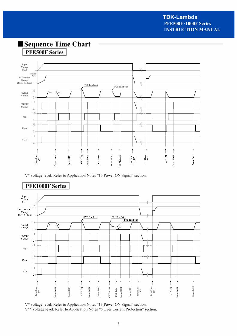
■Sequence Time Chart
PFE500F Series
V* voltage level: Refer to Application Notes “13.Power ON Signal” section.
PFE1000F Series
V* voltage level: Refer to Application Notes “13.Power ON Signal” section. V** voltage level: Refer to Application Notes “6.Over Current Protection” section.
InputVoltage
(AC)
OutputVoltage
BC TerminalVoltage
(Boost Voltage)
L
H
ON/OFFControl
L
H
IOGL
H
ENAL
H
AUXL
H
390VDC(Typ)
V*V*
OVP Trip PointOCP Trip Point
Inpu
t Lin
e O
N
OV
P Tr
ip
LVP
Trip
OC
P A
ctiv
e
Inpu
t Lin
eO
FF
Inpu
t Lin
eO
N
OTP
Trip
Con
trol O
FF
Con
trol O
N
Con
trol O
FF
Con
trol O
N
Con
trol O
FF
Con
trol O
N
Con
trol O
FF
Con
trol O
N

- 4 -
TDK-Lambda PFE500F・1000F Series INSTRUCTION MANUAL
■Terminal Explanation PFE500F Series
[Input side terminals] AC (L) : Input terminal live line AC (N) : Input terminal neutral line +BC : +Boost voltage terminal -BC : -Boost voltage terminal R : External inrush current
limiting resistor terminal
[Output side terminals] +V : +Output terminal -V : -Output terminal +S : +Remote sensing terminal -S : -Remote sensing terminal PC : Output current balance terminal TRIM : Output voltage trimming terminal IOG : Inverter operation good terminal ENA : Power on signal terminal +ON/OFF : +ON/OFF control terminal -ON/OFF : -ON/OFF control terminal AUX : Auxiliary power supply terminal for external circuits COM : Common ground terminal
- Baseplate can be connected to FG through M3 mounting tapped holes. - Consider contact resistance when connecting AC (L), AC (N), R, +BC, -BC, +V, -V. - Note that +BC and -BC terminals is a primary voltage with high voltage (390VDC).
Do not connect load to these terminals. It might result in power module damage.

- 5 -
TDK-Lambda PFE500F・1000F Series INSTRUCTION MANUAL
■Terminal Explanation
PFE1000F Series [Input side terminals] AC (L) : Input terminal live line AC (N) : Input terminal neutral line +BC : +Boost voltage terminal -BC : -Boost voltage terminal R : External inrush current
limiting resistor terminal
[Output side terminals] +V : +Output terminal -V : -Output terminal +S : +Remote sensing terminal -S : -Remote sensing terminal PC : Output current balance terminal TRIM : Output voltage trimming terminal IOG : Inverter operation good terminal ENA : Power on signal terminal +ON/OFF : +ON/OFF control terminal -ON/OFF : -ON/OFF control terminal AUX : Auxiliary power supply terminal for external circuits COM : Common ground terminal
- Baseplate can be connected to FG through M3 mounting tapped holes. - Consider contact resistance when connecting AC (L), AC (N), R, +BC, -BC, +V, -V. - Note that +BC and -BC terminals is a primary voltage with high voltage (390VDC).
Do not connect load to these terminals. It might result in power module damage.

- 6 -
TDK-Lambda PFE500F・1000F Series INSTRUCTION MANUAL
■Explanations on Specifications
1. Input Voltage Range Input voltage range is indicated below. Take care not to apply input voltage which is above this specified range or under
this specified range for more than 30 seconds. Nor should a DC input voltage be applied as this would result into power module damage.
Input Voltage Range : Single Phase 85 to 265VAC Line Frequency Range : 47 to 63Hz ● Basic Connection
Fig. 1-1-(1) Basic Connection for PFE500F Series
Fig. 1-1-(2) Basic Connection for PFE1000F Series Note) To meet the surge immunity, evaluate the addition of the surge protection components. Refer to separate document “PFE500F Series IEC Data” and “PFE1000F Series IEC Data”.
LOAD
PFE1000F
C115
AC(L)
AC(N)
+V
-V
+S
-S
ENA
-BC+BCR
BASE-PLATE
C116
C117
L= 50mm
C118
+
-
C104 C108
C103
C102
Fuse
C101
L101 L102
R101
C110
C109
C112
TFR101
IOGAUX
COM
+ON/OFF-ON/OFF
TRIM
PC
C113
C119
Input Filter(For VCCI-classA)
L103
C105
TFR102
C114
C111
C107
C106

- 7 -
TDK-Lambda PFE500F・1000F Series INSTRUCTION MANUAL
External Input Fuse
This power module has no internal fuse. Use external fuse to acquire each Safety Standard and to further improve safety. Further, Fast-Blow type fuse must be used per one module. Also, in-rush surge current flows during line throw-in. Be sure to check I2t capability of external switch and fuse.
Recommended External Fuse
PFE500F : F15AH, 250V PFE1000F : F25AH, 250V
Note) Select fuse based on rated voltage, rated current and
breaking capacity. (1) Voltage Ratings
100VAC line : AC125V 200VAC line : AC250V
(2) Current Ratings Rated current is selected by the maximum input
current based on operating conditions and can be calculated by the following formula.
(Arms) PFEffVin
Pout(max)Iin ´´
= (Formula 1-1)
Iin (max) : Maximum Input Current Pout : Maximum Output Power Vin : Minimum Input Voltage Eff : Efficiency PF : Power Factor
(3) Breaking Capacity The breaking capacity may be subject to the end use
application. Please select a suitably rated breaking capacity fuse for end use application.
For Efficiency and Power Factor values, refer to separate document “PFE500F Series Evaluation Data” and “PFE1000F Series Evaluation Data”. C1, C4, C5 : 1uF (Film Capacitor) C101, C104, C105, C108 : 1uF (Film Capacitor)
Ripple current flows through this capacitor. When selecting capacitor, be sure to check the allowable maximum ripple current rating of this capacitor. Verify the actual ripple current flowing through this capacitor by doing actual measurement.
Recommended Voltage Rating : 250VAC Note) Connect C5, C108 as near as possible towards the
input terminals of this power module. Audible noise may occur depending on type of film
capacitor. L1, L2 : 6mH L101, L102, L103 : 2mH
Add common mode choke coil to conform to EMI/EMS standard. When using multiple modules, connect coil to each module.
Note) Depending on the input filter used, noise might
increase or power module might malfunction due to filter resonance.
C2, C3, C6, C7, C12: 2,200pF (Ceramic Capacitor) C102, C103 : 470pF (Ceramic Capacitor) C106, C107 : 4,700pF (Ceramic Capacitor)
Connect ceramic capacitor to conform to EMI/EMS standard. Be sure to note the leakage current of your equipment when connecting this capacitor.
High withstand voltage are applied across this capacitor depending on the application. Select capacitors with high withstand voltage rating. R1, R101 : 470kohm
Connect bleeder resistor across AC(L) and AC(N) terminals. C8, C9 : 1uF (Film Capacitor) C109, C110 : 1uF (Film Capacitor)
Ripple current flows through this capacitor. When selecting capacitor, be sure to check the allowable maximum ripple current rating of this capacitor. Verify the actual ripple current flowing through this capacitor by doing actual measurement.
Recommended Voltage Rating : 450VDC Note) Select Capacitor with more than 3A (rms) rating.
Connect C8, C9, C109, C110 as near as possible towards the terminals of this power module.
C10, C11: 390uF (Electrolytic Capacitor) C111, C112, C113, C114 : 390uF (Electrolytic Capacitor)
Refer to “Selection Method of External Bulk Capacitor for Boost Voltage”.
Allowable External Capacitance at nominal capacitor value is shown below.
Recommended Voltage Rating : 450VDC Recommended Total Capacitor :
390uF to 1,200uF (PFE500F Series) 780uF to 2,300uF (PFE1000F Series)
Note) 1. Do not connect capacitors with more than the above capacitance value as this might result in power module damage.
2. When using module between 390uF – 600uF for PFE500F Series, 780uF – 1,200uF for PFE1000F Series total capacitor value, it is necessary to reduce output power as shown in Fig1-3.
3. When using module below -20 deg C ambient temperature, AC ripple of boost voltage, output ripple voltage and start up characteristics might be affected by ESR characteristics of the bulk capacitors. Therefore, be sure to verify characteristics by actual evaluation.
- 8 -
TDK-Lambda PFE500F・1000F Series INSTRUCTION MANUAL
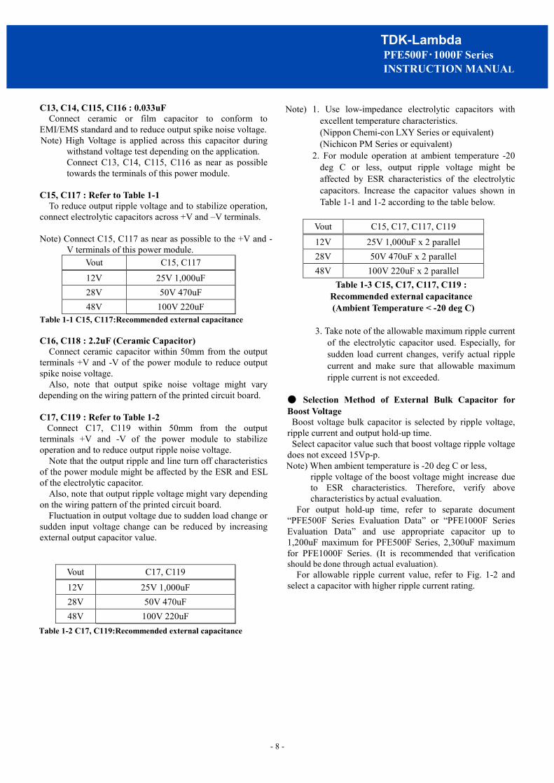
C13, C14, C115, C116 : 0.033uF
Connect ceramic or film capacitor to conform to EMI/EMS standard and to reduce output spike noise voltage. Note) High Voltage is applied across this capacitor during
withstand voltage test depending on the application. Connect C13, C14, C115, C116 as near as possible towards the terminals of this power module.
C15, C117 : Refer to Table 1-1 To reduce output ripple voltage and to stabilize operation,
connect electrolytic capacitors across +V and –V terminals.
Note) Connect C15, C117 as near as possible to the +V and -V terminals of this power module.
Vout C15, C117
12V 25V 1,000uF 28V 50V 470uF 48V 100V 220uF
Table 1-1 C15, C117:Recommended external capacitance C16, C118 : 2.2uF (Ceramic Capacitor)
Connect ceramic capacitor within 50mm from the output terminals +V and -V of the power module to reduce output spike noise voltage.
Also, note that output spike noise voltage might vary depending on the wiring pattern of the printed circuit board. C17, C119 : Refer to Table 1-2
Connect C17, C119 within 50mm from the output terminals +V and -V of the power module to stabilize operation and to reduce output ripple noise voltage.
Note that the output ripple and line turn off characteristics of the power module might be affected by the ESR and ESL of the electrolytic capacitor.
Also, note that output ripple voltage might vary depending on the wiring pattern of the printed circuit board.
Fluctuation in output voltage due to sudden load change or sudden input voltage change can be reduced by increasing external output capacitor value.
Vout C17, C119
12V 25V 1,000uF 28V 50V 470uF 48V 100V 220uF
Table 1-2 C17, C119:Recommended external capacitance
Note) 1. Use low-impedance electrolytic capacitors with
excellent temperature characteristics. (Nippon Chemi-con LXY Series or equivalent) (Nichicon PM Series or equivalent)
2. For module operation at ambient temperature -20 deg C or less, output ripple voltage might be affected by ESR characteristics of the electrolytic capacitors. Increase the capacitor values shown in Table 1-1 and 1-2 according to the table below.
Vout C15, C17, C117, C119
12V 25V 1,000uF x 2 parallel 28V 50V 470uF x 2 parallel 48V 100V 220uF x 2 parallel
Table 1-3 C15, C17, C117, C119 : Recommended external capacitance
(Ambient Temperature < -20 deg C)
3. Take note of the allowable maximum ripple current of the electrolytic capacitor used. Especially, for sudden load current changes, verify actual ripple current and make sure that allowable maximum ripple current is not exceeded.
● Selection Method of External Bulk Capacitor for Boost Voltage
Boost voltage bulk capacitor is selected by ripple voltage, ripple current and output hold-up time.
Select capacitor value such that boost voltage ripple voltage does not exceed 15Vp-p. Note) When ambient temperature is -20 deg C or less,
ripple voltage of the boost voltage might increase due to ESR characteristics. Therefore, verify above characteristics by actual evaluation.
For output hold-up time, refer to separate document “PFE500F Series Evaluation Data” or “PFE1000F Series Evaluation Data” and use appropriate capacitor up to 1,200uF maximum for PFE500F Series, 2,300uF maximum for PFE1000F Series. (It is recommended that verification should be done through actual evaluation).
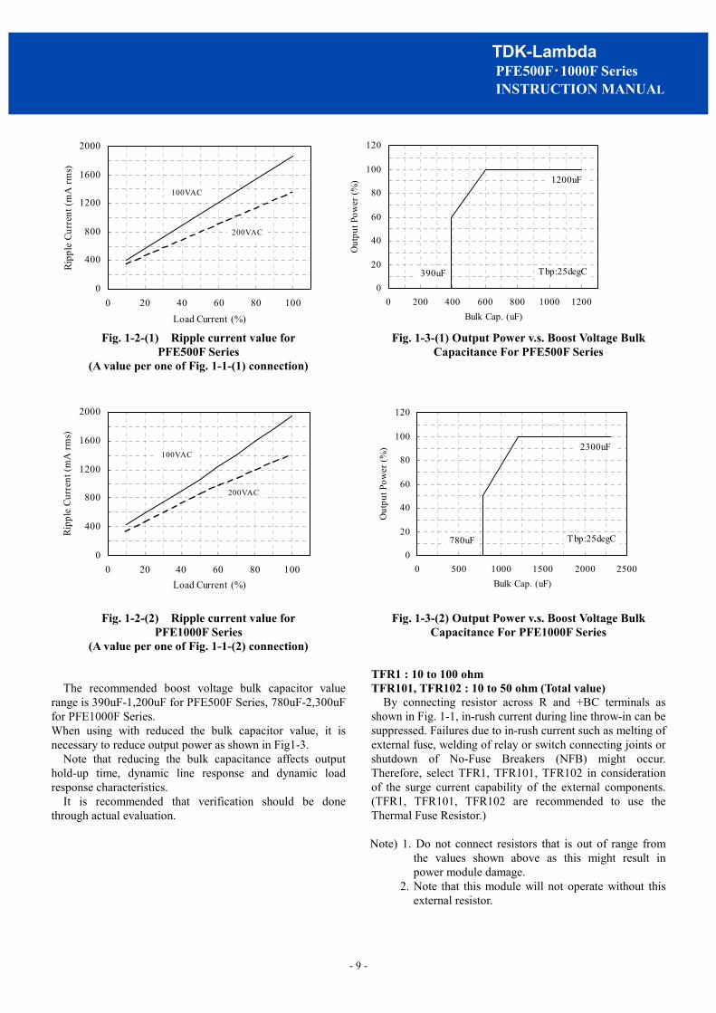
For allowable ripple current value, refer to Fig. 1-2 and select a capacitor with higher ripple current rating.
- 9 -
TDK-Lambda PFE500F・1000F Series INSTRUCTION MANUAL
0
400
800
1200
1600
2000
0 20 40 60 80 100Load Current (%)
Ripp
le C
urre
nt (m
A rm
s)
100VAC
200VAC
0
20
40
60
80
100
120
0 200 400 600 800 1000 1200Bulk Cap. (uF)
Out
put P
ower
(%)
390uF
1200uF
Tbp:25degC
Fig. 1-2-(1) Ripple current value for
PFE500F Series (A value per one of Fig. 1-1-(1) connection)
Fig. 1-2-(2) Ripple current value for PFE1000F Series
(A value per one of Fig. 1-1-(2) connection)
The recommended boost voltage bulk capacitor value range is 390uF-1,200uF for PFE500F Series, 780uF-2,300uF for PFE1000F Series. When using with reduced the bulk capacitor value, it is necessary to reduce output power as shown in Fig1-3.
Note that reducing the bulk capacitance affects output hold-up time, dynamic line response and dynamic load response characteristics.
It is recommended that verification should be done through actual evaluation.
Fig. 1-3-(1) Output Power v.s. Boost Voltage Bulk Capacitance For PFE500F Series
Fig. 1-3-(2) Output Power v.s. Boost Voltage Bulk Capacitance For PFE1000F Series
TFR1 : 10 to 100 ohm TFR101, TFR102 : 10 to 50 ohm (Total value)
By connecting resistor across R and +BC terminals as shown in Fig. 1-1, in-rush current during line throw-in can be suppressed. Failures due to in-rush current such as melting of external fuse, welding of relay or switch connecting joints or shutdown of No-Fuse Breakers (NFB) might occur. Therefore, select TFR1, TFR101, TFR102 in consideration of the surge current capability of the external components. (TFR1, TFR101, TFR102 are recommended to use the Thermal Fuse Resistor.)
Note) 1. Do not connect resistors that is out of range from
the values shown above as this might result in power module damage.
2. Note that this module will not operate without this external resistor.
0
400
800
1200
1600
2000
0 20 40 60 80 100Load Current (%)
Ripp
le C
urre
nt (m
A rm
s)
100VAC
200VAC
0
20
40
60
80
100
120
0 500 1000 1500 2000 2500Bulk Cap. (uF)
Out
put P
ower
(%)
780uF
2300uF
Tbp:25degC
- 10 -
TDK-Lambda PFE500F・1000F Series INSTRUCTION MANUAL
●Selection Method of External Resistor (1) Calculating Resistance Value for External Resistor
Resistance can be calculated by the formula below.
)(IrushVinR Ω = (Formula 1-2)
R : Resistance Value for External resistor Vin : Input Voltage converted to DC value
=Input Votlage (rms) x 2 Irush : Input surge current value
(2) Required Surge Current Rating Sufficient surge current withstand capability is required for external resistor. Required Surge Current Rating can be selected by I2t. (Current squared multiplied by time)
)sA(R2
VinCotI 22
2 ´
´= (Formula 1-3)
I2t : Current-squared multiplied by time Co : Boost Voltage Bulk Capacitance Vin : Input Voltage converted to DC value
=Input Voltage (rms) x 2 R : Resistance Value for External Resistor
2. Output Voltage Adjustment Range
(TRIM terminal) Output voltage can be adjusted within the range below by
connecting fixed and variable resistors or applying external voltage.
However, take care not to exceed the output voltage range shown below because OVP function will activate.
In the PFE1000F Series, be careful not to drop from the following range, because a Low Voltage Protection (LVP) function will be activate.
Output Voltage Adjustment Range :
+/-20% of the typical voltage rating
When increasing or decreasing output voltage, it must not exceed maximum output current and power.
Even if the output voltage is adjusted using external circuit shown in Fig. 2-1, remote sensing can be done. For details on Remote Sensing function, refer to “9. Remote Sensing”. Output Voltage Adjustment using Fixed and Variable Resistors
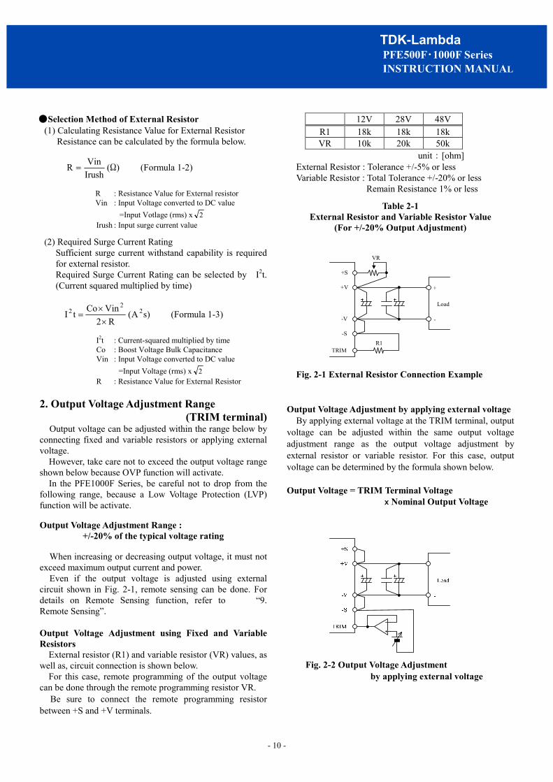
External resistor (R1) and variable resistor (VR) values, as well as, circuit connection is shown below.
For this case, remote programming of the output voltage can be done through the remote programming resistor VR. Be sure to connect the remote programming resistor between +S and +V terminals.
12V 28V 48V R1 18k 18k 18k VR 10k 20k 50k
unit:[ohm] External Resistor : Tolerance +/-5% or less Variable Resistor : Total Tolerance +/-20% or less Remain Resistance 1% or less
Table 2-1 External Resistor and Variable Resistor Value
(For +/-20% Output Adjustment)
Fig. 2-1 External Resistor Connection Example Output Voltage Adjustment by applying external voltage By applying external voltage at the TRIM terminal, output voltage can be adjusted within the same output voltage adjustment range as the output voltage adjustment by external resistor or variable resistor. For this case, output voltage can be determined by the formula shown below. Output Voltage = TRIM Terminal Voltage x Nominal Output Voltage
Fig. 2-2 Output Voltage Adjustment by applying external voltage
+S
-S
+V
-V
TRIM
+
-
Load
R1
VR

- 11 -
TDK-Lambda PFE500F・1000F Series INSTRUCTION MANUAL
For applications other than the above, refer to the TRIM circuit as shown in fig.2-3 and determine external circuit and components values.
Fig.2-3 Internal TRIM Circuit (For the Reference) 3. Maximum Ripple and Noise
This value is measured according to the description below in accordance with JEITA-9131B(Section 7.16, 7.17 and 7.18).
In the basic connection shown in Fig. 1-1, additional connection shown in Fig. 3-1 is done for measurement. Capacitor (Ceramic Capacitor : 2.2µF and Electrolytic Capacitor : Refer to Table 1-2) must be connected within 50mm from the output terminals. Then, connect coaxial cable with JEITA attachment across the ceramic capacitor electrodes. Use 100MHz bandwidth oscilloscope or equivalent.
Also, note that output ripple voltage and output spike noise voltage might vary depending on the wiring pattern of the printed circuit board. In general, output ripple voltage and output spike noise voltage can be reduced by increasing external capacitance.
Fig. 3-1 Output Ripple Voltage (including Spike Noise)
Measurement Method 4. Maximum Line Regulation
Maximum line regulation is defined as the maximum output voltage change when input voltage is gradually changed (Steady-State) within specification range.
5. Maximum Load Regulation
Maximum load regulation is defined as the maximum output voltage change when output load current is gradually changed (Steady-State) within specification range.
When using power module in dynamic load mode, audible sound could be heard from the power module or large output voltage change might occur. Make prior evaluation thoroughly before using this power module.
6. Over Current Protection (OCP)
This module is equipped with OCP function. Constant current limiting with automatic recovery for
PFE500F Series. Output will automatically recover when short circuit or overload condition is released.
Constant current limiting with delay shutdown for PFE1000F Series. Output will be shutdown when output about under 70% by short circuit or overload condition that continue about 0.5s. When the shutdown function activates, first cut off input line and verify that boost voltage has dropped down to 20V or less. Then, recover output by recycling input line. In other method, reset to ON/OFF control. OCP value is fixed and cannot be adjusted externally.
Note that continuous short circuit or overload condition more than 30s, might result in power module damage. 7. Over Voltage Protection (OVP)
This module is equipped with OVP function. This value is set between 125% to 145% of nominal output voltage.
When the OVP function activates, first cut off input line and verify that boost voltage has dropped down to 20V or less. Then, recover output by recycling input line. In other method, reset to ON/OFF control. OVP value is fixed and cannot be set externally.
8. Over Temperature Protection (OTP)
This module is equipped with OTP function. This function activates and shuts down the output when ambient temperature or internal temperature abnormal rises. OTP activates at following baseplate temperature.
PFE500F-12 : 90 to 115 deg C PFE500F-28, 48 : 105 to 130 deg C PFE1000F-* : 105 to 130 deg C
When OTP function operates, output can be recovered by
cooling down the baseplate sufficiently and letting the boost voltage drop down to 20V or less before recycling the input line. In other method, reset to ON/OFF control.
7.32kΩ
32.4kΩ 1kΩ
1.225VReference
voltage
+S
-S
TRIM
Error amplifier
- 12 -
TDK-Lambda PFE500F・1000F Series INSTRUCTION MANUAL
9. Remote Sensing (+S, -S terminals)
This module has remote sensing terminals to compensate for voltage line drop from the output terminals to the output load. When remote sensing is not required, (local sensing) short +S to +V and -S to -V terminals respectively.
Note that line drop (voltage drop due to wiring ) compensation voltage range must be such that the output voltage is within the output voltage adjustment range and that the voltage between -V and -S must be within 0.5V.
Consider power loss due to line drop and use power module within the maximum allowable output power. Reduce the effect of noise to the remote sensing line by using a shield line, a twist pair, or a parallel pattern, etc.
When remote sensing line is long, add the electrolytic capacitor as shown in Fig 9-1.
Fig. 9-1 Remote Sensing is used
Fig. 9-2 Remote Sensing is not used (Local Sensing)
10. ON/OFF Control (+ON/OFF, -ON/OFF terminal)
This module is equipped with ON/OFF control function. Without turning the input supply on and off, the output can be enabled and disabled using this function.
The ON/OFF control circuit is isolated from input circuit of the power supply by photo-coupler.
Fig. 10-1 and Fig. 10-2 is connection example of ON/OFF control. When the ON/OFF control is not used, short +ON/OFF to AUX and -ON/OFF to COM terminals respectively.
Fig. 10-1 ON/OFF Control Connection Example 1
(ON/OFF Control by External Voltage)
Select the external voltage and external resistance, as the ON/OFF terminals current is shown below.
ON/OFF terminal current Output Voltage 2.5mA (+/-0.5mA) ON Less than 0.15mA OFF
Table 10-1 Recommended ON/OFF Terminal Current
Fig. 10-2 ON/OFF Control Connection Example 2
(ON/OFF Control by Built-in AUX)
Fig. 10-3 ON/OFF Control Connection Example 3
(ON/OFF Control is not used)
+S
-S
-V
+V
Load
+
-
Twist pair
Stabilize the output voltage at load terminal
External voltage
-ON/OFF
+ON/OFF
AUX
COM
4.7k
ON
OFF
R
11V
-ON/OFF
+ON/OFF
AUX
COM
4.7k
11V

- 13 -
TDK-Lambda PFE500F・1000F Series INSTRUCTION MANUAL
11. Series Operation Series operation is possible for PFE500F Series and
PFE1000F Series. Connections shown in Fig. 11-1 and Fig. 11-2 are possible.
Fig. 11-1 Series Operation for High Output Voltage Applications
Fig. 11-2 +/-Output Series Applications 12. Parallel Operation (PC terminal)
By connecting the PC terminal of each power module, output current can be equally drawn from each module. A maximum of 6 units of the same model can be connected.
However, maximum output current is derated by parallel operation units as shown in Table 12-1.
Note that usage of power module at out-of-rated condition might result in power module temperature abnormal rise or damage.
Parallel units Maximum output current ~3 units 90% of nominal output current
4~6 units 85% of nominal output current Table 12-1 Condition for Parallel Operation
Set the accuracy of the output voltage within +/-1% when
adjust the output voltage for parallel operation. When adjust the output voltage by applying external
voltage at the TRIM terminal, insert a about 10k ohm resistor between TRIM terminal and external source.
Moreover, external circuits are necessary for TRIM terminal at each individual module.
Fig. 12-1 Output Voltage Adjustment by applying external voltage
(For parallel operation)
At parallel operation, +BC, -BC and R terminals must not be connected in parallel with other modules. It might result in power module damage.
Refer to “Parallel Operation” of the Power Module Application Notes for details.
13. Power ON Signal (ENA terminal)
This signal is located at the secondary side (output side) and it is an open collector output. (Maximum sink current is 10mA and maximum applied voltage is 75V.)
Return line for ENA terminal is the COM terminal. When output voltage goes over a specified voltage level at
start up, Power ON signal is LOW. Output voltage threshold level is as follows.
PFE500F・1000F-12 : 8V (TYP) PFE500F・1000F-28 : 19V (TYP) PFE500F・1000F-48 : 33V (TYP)
On the other hand, output voltage threshold level for Power ON signal to turn HIGH is as follows.
PFE500F・1000F-12 : 6V (TYP) PFE500F・1000F-28 : 15V (TYP) PFE500F・1000F-48 : 28V (TYP)
14. I.O.G signal (IOG terminal)
Normal or abnormal operation of the power module can be monitored by using the IOG terminal. Output of this signal monitor is located at secondary side (output side) and is an open collector output.
This signal is LOW when inverter is normally operating and HIGH when inverter stops or when inverter is operating abnormally. (maximum sink current is 5mA, maximum applied voltage is 35V)
Ground for the IOG terminal is the COM terminal. Also note that IOG becomes unstable for following
conditions: ・Operation of Over Current Protection (OCP) ・Light load conditions at parallel operation ・Dynamic load operation
+S
-S-V
+V
Load
+
-
+S+V
-S-V

- 14 -
TDK-Lambda PFE500F・1000F Series INSTRUCTION MANUAL
15. Auxiliary power supply for external circuits (AUX terminal)
For AUX terminal, output voltage value is within 10~14VDC range, maximum output current is 20mA. Ground for the AUX terminal is COM terminal. Avoid short circuit of AUX terminal with other terminals as this would lead to power module damage. 16.Operating Temperature Range
These products can be used in any mounting direction but be sure to consider enough airflow to avoid heat accumulation around the module.
Consider surrounding components layout and set the PCB mounting direction such that air can flow through the heatsink by forced or convection cooling .
This product can operate at actual mounting condition when baseplate temperature is maintained at or below the following baseplate temperature.
PFE500F-12 : 85 deg C PFE500F-28,48 : 100 deg C PFE1000F-12 : 100 deg C PFE1000F-28,48 : 85 deg C (85VAC≦Vin<170VAC)
100 deg C (170VAC≦Vin≦265VAC) Verify baseplate temperature at worst case operating
condition at the measuring point as shown in Fig. 16-1. For Thermal Design details, refer to Power Module
Application Notes “Thermal Design” section. Fig. 16-1 Baseplate Measuring Point
Baseplate temperature range is limited according to Fig. 16-2.
Fig. 16-2-(1) PFE500F Series Derating Curve
Fig. 16-2-(2) PFE1000F-12 Derating Curve
Fig. 16-2-(3) PFE1000F-28,48 Derating Curve
To further improve the reliability, it is recommended to use this module with baseplate temperature derating. 17. Operating Humidity Note that dewdrop might cause power module abnormal operation or damage. 18. Storage Temperature Note that rapid temperature change causes dewdrop causing harmful effect on soldering condition of the terminal pins. 19. Storage Humidity
Storage under high temperature and high humidity causes rust on terminal pins that causes deterioration of soldering conditions. Take enough caution when storing this module. 20. Cooling Method
For details of thermal design, refer to Power Module Application Notes “Thermal Design” section.
Load(%
)Lo
ad(%
)

- 15 -
TDK-Lambda PFE500F・1000F Series INSTRUCTION MANUAL
21. Withstand Voltage
This module is designed to withstand applied voltage 2.5kVAC between input and baseplate, 3kVAC between input and output for a duration of 1 minute. When doing this test during incoming inspection, set the current limit of test equipment to 20mA.
This module is designed to withstand applied voltage 500VDC between output and baseplate for 1 minute. When doing this test during incoming inspection, be sure to apply DC voltage only. Avoid applying AC voltage during this test because this will damage the module. Refrain from injecting high test voltage suddenly. Be sure to gradually increase the applied voltage during testing and gradually reduce the voltage after the test. Especially, when using timer switch of the test equipment, impulse voltage which is higher than the applied set voltage, is generated when the timer switch is cut off. This causes damage to the power module. Connect each terminal according to the circuit diagram shown below. For basic connection shown in Fig. 1-1, do the same terminal connections.
2.5kVAC 1 minute (20mA) Fig. 21-1 Input to Baseplate Withstand Voltage
Test Method
3kVAC 1 minute (20mA) Fig.21-2 Input to Output Withstand Voltage
Test Method
500VDC 1 minute
Fig.21-3 Output to Baseplate Withstand Voltage Test Method
22. Insulation Resistance Use DC Insulation Resistance test equipment (MAX.500V) between output and baseplate.
Insulation Resistance must be 100Mohm or more at 500VDC. Take caution that some types of test equipment generate high pulse voltage when switching applied voltage. After test, discharge this module using resistor, etc.
100Mohm or more at 500VDC Fig. 22-1 Insulation Resistance Test Method
23. Recommended Soldering Condition
Recommended soldering temperature is as follows. (1) Soldering Dip :
260℃, within 10 seconds Preheat :
130℃, within 60 seconds (2) Soldering iron :
350℃, within 3 seconds
Withstand voltagetester
BASE-PLATE
AC(N)
AC(L)
R +BC -BC
+V-V
+S-S
PCTRIM
IOGENAAUX
+ON/OFF-ON/OFF
COM
PFE500FPFE1000F
- 16 -
TDK-Lambda PFE500F・1000F Series INSTRUCTION MANUAL
Verify following items before concluding power module damage. 1) No output voltage - Is specified input voltage applied? - During output voltage adjustment, is the fixed resistor or variable resistor setting correct? - Is there no abnormality with the output load? - Is the actual baseplate temperature within the
specified operating temperature of this module? - Are the ON/OFF control terminals (+ON/OFF, -ON/OFF) correctly connected? 2) Output voltage is high - Are the remote sensing terminals (+S, -S) correctly connected? - Is the measurement done at the sensing points? - During output voltage adjustment, is the fixed resistor
or variable resistor setting correct? 3) Output voltage is low - Is specified input voltage applied? - Are the remote sensing terminals (+S, -S) correctly connected? - Is the measurement done at the sensing points? - During output voltage adjustment, is the fixed resistor or variable resistor setting correct? - Is there no abnormality with the output load? 4) Load regulation or line regulation is large - Is specified input voltage applied? - Are the input or output terminals firmly connected? - Is the measurement done at the sensing points? - Are the input and output wires too thin? 5) Large output ripple - Is the measurement done according to methods
described Application Notes or is it an equivalent method?
■ Before Concluding Power Module Damage