
Inkjet Fabrication of Copper Patterns for Flexible ...
10
Inkjet Fabrication of Copper Patterns for Flexible Electronics: Using Paper with Active Precoatings Thomas O ̈ hlund,* ,† Anna K. Schuppert, ‡ Magnus Hummelga ̊ rd, † Joakim Ba ̈ ckströ m, † Hans-Erik Nilsson, § and Ha ̊ kan Olin † † Department of Natural Sciences, Mid Sweden University, SE-85170 Sundsvall, Sweden ‡ Institut Charles Gerhardt de Montpellier - UMR 5253, 34095 Montpellier Cedex 5, France § Department of Electronics Design, Mid Sweden University, SE-85170 Sundsvall, Sweden * S Supporting Information ABSTRACT: Low-cost solution-processing of highly conduc- tive films is important for the expanding market of printed electronics. For roll-to-roll manufacturing, suitable flexible substrates and compatible postprocessing are essential. Here, custom-developed coated papers are demonstrated to facilitate the inkjet fabrication of high performance copper patterns. The patterns are fabricated in ambient conditions using water-based CuO dispersion and intense pulsed light (IPL) processing. Papers using a porous CaCO 3 precoating, combined with an acidic mesoporous absorption coating, improve the effective- ness and reliability of the IPL process. The processing is realizable within 5 ms, using a single pulse of light. A resistivity of 3.1 ± 0.12 μΩ·cm is achieved with 400 μm wide conductors, corresponding to more than 50% of the conductivity of bulk copper. This is higher than previously reported results for IPL-processed copper. KEYWORDS: intense pulsed light sintering, flash light sintering, printed flexible electronics, inkjet printing, paper coatings, copper patterns, IPL sintering, IPL processing 1. INTRODUCTION Printed electronics is an emerging manufacturing technology that has gained considerable interest in recent years. Reductions in cost and energy consumption, as well as less material waste, are important driving forces. In addition, the possibility to utilize low-cost flexible substrates and roll-to-roll manufacturing, further increases the competitiveness and potential application range. Electrically conducting thin films are important because they are fundamental parts of most printed circuits and devices such as conductive tracks, 1 antennas 2 and electrodes for sensors, 3 light- emitting devices, 4 displays 5 and solar cells. 6 Conductive inkjet inks either contain conductive polymers, 7−9 carbon-based materials 10,11 or metal-based materials. 12−18 A high conductivity is usually desired and often crucial for the device performance, particularly for large-area devices. Metal-based inks offer unmatched performance in this regard; a resistivity of only 1.1−1.3 times the bulk metal has been achieved. 19 Silver nano- particle (AgNP) ink is a common choice, due to a high con- ductivity and good stability in ambient conditions. However, the high cost of AgNP ink is problematic for cost-sensitive applications or large area coverage. Bulk Cu offers 95% of the electrical conductivity of Ag, 20 for a fraction of the cost. Therefore, CuNP ink formulations are potentially more cost-effective. However, the reactivity of CuNPs in ambient conditions makes ink development and postprocessing challenging compared to Ag. Li et al. 14 demonstrated reactive printing of Cu films on paper by the simultaneous printing of aqueous Cu-citrate solution and reducing agent, using thermal inkjet. Park et al. 15 synthesized CuNPs that were stable in solution, which they attributed to protection from oxidation by the polyvinylpyrrolidone (PVP) stabilizing agents. However, the sintering had to be performed in a vacuum to avoid oxidation. Efforts have been made to decrease reactivity by coating CuNPs with thin layers of less reactive materials, such as Ag 16 and C. 17 Nevertheless, oxidation remains an issue during oven-sintering in ambient conditions. Although low-temperature reduction and sintering has been shown with printed CuNP films, the resistivity has been at best 30−50 times larger than the bulk value. 14,17 Roll-to-roll processes using low-cost plastic- or paper-based substrates require postprocessing that is quick and effective, as well as compatible with ambient conditions and temperature- sensitive substrates. Intense pulsed light processing (IPL) is a suitable method that briefly induces high film temperature by flash lamp exposure. Using a pulse duration of a few milliseconds or less, the heat transfer to the underlying substrate can be limited, avoiding damage. Thermal simulations estimated that a 300 μs flash pulse induces a film temperature exceeding 1000 °C, for a 1 μm thick silver film on top of a 150 μm thick substrate of polyethylene Received: April 8, 2015 Accepted: August 6, 2015 Published: August 6, 2015 Research Article www.acsami.org © 2015 American Chemical Society 18273 DOI: 10.1021/acsami.5b03061 ACS Appl. Mater. Interfaces 2015, 7, 18273−18282 Downloaded by MID SWEDEN UNIV on September 14, 2015 | http://pubs.acs.org Publication Date (Web): August 13, 2015 | doi: 10.1021/acsami.5b03061
Transcript of Inkjet Fabrication of Copper Patterns for Flexible ...
Inkjet Fabrication of Copper Patterns for Flexible Electronics:Using Paper with Active PrecoatingsThomas Ohlund,*,† Anna K. Schuppert,‡ Magnus Hummelgard,† Joakim Backstrom,† Hans-Erik Nilsson,§
and Hakan Olin†
†Department of Natural Sciences, Mid Sweden University, SE-85170 Sundsvall, Sweden‡Institut Charles Gerhardt de Montpellier - UMR 5253, 34095 Montpellier Cedex 5, France§Department of Electronics Design, Mid Sweden University, SE-85170 Sundsvall, Sweden
*S Supporting Information
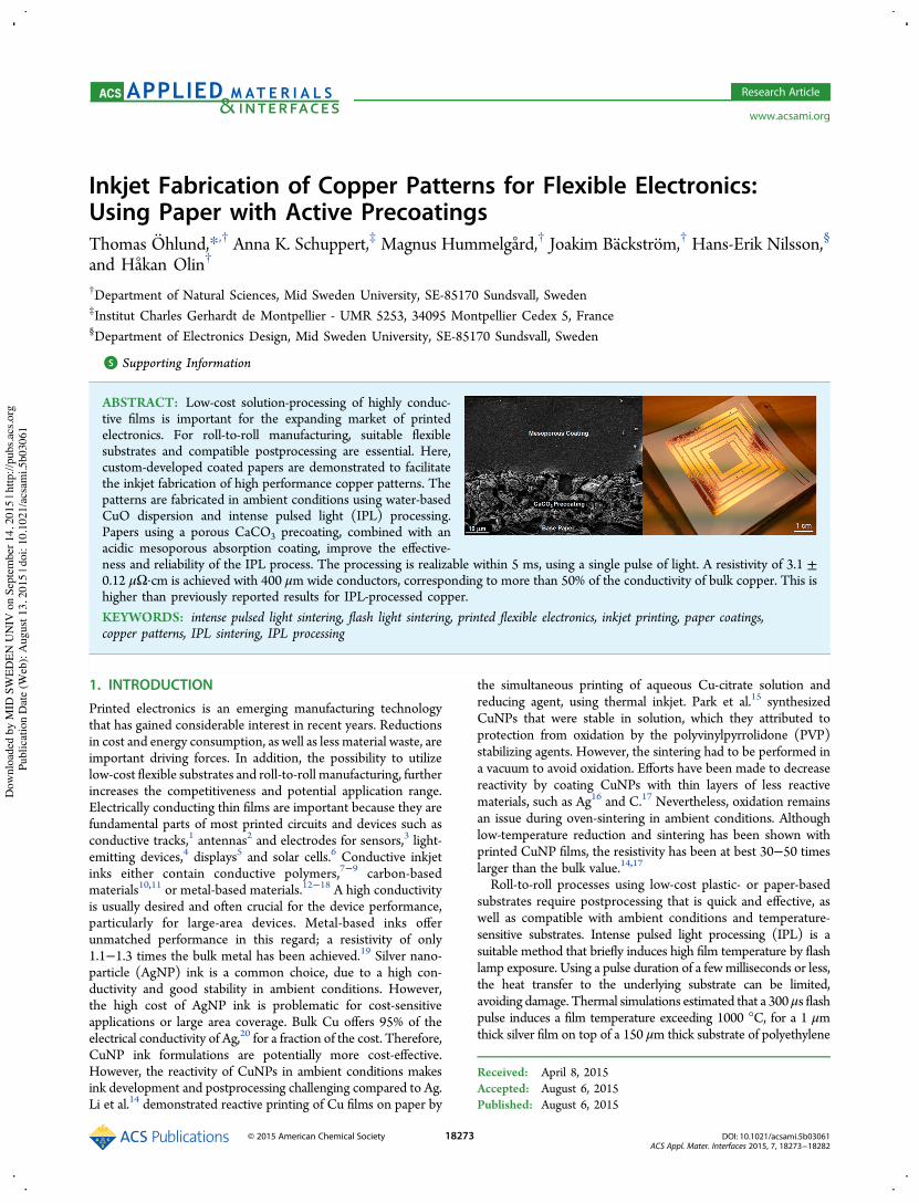
ABSTRACT: Low-cost solution-processing of highly conduc-tive films is important for the expanding market of printedelectronics. For roll-to-roll manufacturing, suitable flexiblesubstrates and compatible postprocessing are essential. Here,custom-developed coated papers are demonstrated to facilitatethe inkjet fabrication of high performance copper patterns. Thepatterns are fabricated in ambient conditions using water-basedCuO dispersion and intense pulsed light (IPL) processing.Papers using a porous CaCO3 precoating, combined with anacidic mesoporous absorption coating, improve the effective-ness and reliability of the IPL process. The processing is realizable within 5 ms, using a single pulse of light. A resistivity of 3.1 ±0.12 μΩ·cm is achieved with 400 μm wide conductors, corresponding to more than 50% of the conductivity of bulk copper. This ishigher than previously reported results for IPL-processed copper.KEYWORDS: intense pulsed light sintering, flash light sintering, printed flexible electronics, inkjet printing, paper coatings,copper patterns, IPL sintering, IPL processing
1. INTRODUCTIONPrinted electronics is an emerging manufacturing technologythat has gained considerable interest in recent years. Reductionsin cost and energy consumption, as well as less material waste, areimportant driving forces. In addition, the possibility to utilizelow-cost flexible substrates and roll-to-roll manufacturing, furtherincreases the competitiveness and potential application range.Electrically conducting thin films are important because they arefundamental parts of most printed circuits and devices such asconductive tracks,1 antennas2 and electrodes for sensors,3 light-emitting devices,4 displays5 and solar cells.6 Conductive inkjetinks either contain conductive polymers,7−9 carbon-basedmaterials10,11 or metal-based materials.12−18 A high conductivityis usually desired and often crucial for the device performance,particularly for large-area devices. Metal-based inks offerunmatched performance in this regard; a resistivity of only1.1−1.3 times the bulk metal has been achieved.19 Silver nano-particle (AgNP) ink is a common choice, due to a high con-ductivity and good stability in ambient conditions. However,the high cost of AgNP ink is problematic for cost-sensitiveapplications or large area coverage. Bulk Cu offers 95% of theelectrical conductivity of Ag,20 for a fraction of the cost. Therefore,CuNP ink formulations are potentially more cost-effective.However, the reactivity of CuNPs in ambient conditions makesink development and postprocessing challenging compared to Ag.Li et al.14 demonstrated reactive printing of Cu films on paper by
the simultaneous printing of aqueous Cu-citrate solution andreducing agent, using thermal inkjet. Park et al.15 synthesizedCuNPs that were stable in solution, which they attributed toprotection from oxidation by the polyvinylpyrrolidone (PVP)stabilizing agents. However, the sintering had to be performed ina vacuum to avoid oxidation. Efforts have been made to decreasereactivity by coating CuNPs with thin layers of less reactivematerials, such as Ag16 and C.17 Nevertheless, oxidation remainsan issue during oven-sintering in ambient conditions. Althoughlow-temperature reduction and sintering has been shown withprinted CuNP films, the resistivity has been at best 30−50 timeslarger than the bulk value.14,17
Roll-to-roll processes using low-cost plastic- or paper-basedsubstrates require postprocessing that is quick and effective, aswell as compatible with ambient conditions and temperature-sensitive substrates. Intense pulsed light processing (IPL) is asuitable method that briefly induces high film temperature by flashlamp exposure. Using a pulse duration of a fewmilliseconds or less,the heat transfer to the underlying substrate can be limited,avoiding damage. Thermal simulations estimated that a 300μs flashpulse induces a film temperature exceeding 1000 °C, for a 1 μmthick silver film on top of a 150 μm thick substrate of polyethylene
Received: April 8, 2015Accepted: August 6, 2015Published: August 6, 2015
Research Article
www.acsami.org
© 2015 American Chemical Society 18273 DOI: 10.1021/acsami.5b03061ACS Appl. Mater. Interfaces 2015, 7, 18273−18282
Dow
nloa
ded
by M
ID S
WED
EN U
NIV
on
Sept
embe
r 14,
201
5 | h
ttp://
pubs
.acs
.org
P
ublic
atio
n D
ate
(Web
): A
ugus
t 13,
201
5 | d
oi: 1
0.10
21/a
csam
i.5b0
3061
terephthalate (PET).21 According to the simulation, the PETsubstrate temperature never exceeds 250 °C, and falls below150 °C within 8 ms. For CuNP films, IPL processing isparticularly suitable, because oxide impurities can be effectivelyreduced due to the high peak temperature, if a reducing agent ispresent. Some commonly used ink solvents, such as ethanoland ethylene glycol can function as reducing agents, but to avoidreoxidation the pulse duration needs to be sufficiently short.22
Dharmadasa et al.22 used IPL processing with CuNP ink films,spray-coated on PET and glass. They observed that no reoxida-tion occurred with a pulse duration of 2 ms. The Cu2O impuritiesof unsintered films were significant when using water as a solvent,but much less when using ethylene glycol. Ryu et al.23 suggestedthat PVP will act as a reducing agent during IPL processing whenused as a colloidal stabilizer for Cu/Cu2O NPs. They proposedthat PVP is decomposed by UV irradiation into an inter-mediate weak acid and/or hydroxyl end groups, acting likealcohol reductants. Araki et al.24 developed different organicCu-salt precursor inks that were screen printed on glass andprocessed with IPL. The Cu-salt precursor with the longesthydrocarbon chain length had the largest light absorption butstill the highest resulting resistivity. The authors believed it wasdue to the evaporation of carbon that damaged the films, andto residual carbon remaining after sintering. Other interestingstudies were performed by Hwang et al.,25 who monitored theIPL sintering of a CuNP ink in situ; and Chung et al.,26 whoexamined the IPL sintering of Cu precursor/CuNP hybrid inks.One of the most promising methods of Cu film fabrication is
the IPL processing of CuONPs.27,28 CuONPs are less reactive indispersion than the CuNP counterpart, and stable water-basedinks have been made commercially available. Further, CuO NPinks can be acquired commercially at much lower cost (currently75$/kg in bulk quantities29) than CuNP- or AgNP inks.Inkjet printing technology is scalable to cover large areas and
can be integrated into existing production environments at acomparably low cost. Inkjet is a noncontact method and thereforeavoids contamination or damage to the substrates or previouslydeposited layers. Further, it is digital in its nature, which meansthat changes in the deposited patterns can be made quickly andeasily. Inkjet requires a comparably low ink viscosity, the viablerange for piezoelectric inkjet is approximately 5−30 mPa·s.30
Low viscosity usually implies a low volume concentration ofactive material; therefore, a large amount of ink solvent needsto be quickly evaporated, or absorbed into the substrate. Quickevaporation from the substrate is possible by using volatile inksolvents and/or substrate heating. However, this also increasesthe evaporation rate at the nozzle−air interface, increasing the riskof inkjet nozzle clogging and therefore compromising the printingreliability. Furthermore, substrate heating is energy-consuming,and nontrivial to integrate in roll-to-roll environments. Utilizingabsorption is an attractive alternative, in which paper substrateshave inherent advantages. Besides the absorption capability, otheradvantages of paper are flexibility, low-cost and environmentalsustainability. Inkjet-printed functional layers on paper typicallyrequire a high quality coating to reduce the surface roughness.With a suitable coating, the absorption rate can be increased aswell, improving both pattern definition and functional perform-ance.31 Mesoporous coatings have been found particularly wellsuited for inkjet-printing of metal nanoparticle inks, because theyprovide a smooth surface combined with a high absorption rate.32
Paper substrates have previously been specially designedfor the application in printed electronics.33,34 Bollstrom et al.33
developed a paper design with a thin smooth top coating.
The authors paid special attention to precoatings with goodbarrier properties, to ensure suitability for organic semiconductorinks in various applications. However, paper substrates thatfacilitate IPL processing of NP-based inks have not beenconsidered previously. In this study, we exploit a paper designusing a mesoporous coating that is suitable for inkjet-printingof NP-based inks. Moreover, the paper design utilizes a novel,porous CaCO3 precoating that increase the absorption and altersthe surface chemistry. Recently, we showed that this paper designassisted low-temperature sintering of AgNP ink.35 Here wedemonstrate that the CaCO3 precoating enhances reliability andeffectiveness during IPL processing of CuO, thereby substantiallyimproving the performance of inkjet-printed copper films.
2. EXPERIMENTAL SECTION2.1. Manufacturing of Coated Paper Substrates. Two series of
inkjet papers with mesoporous absorption coatings were manufactured.Each paper consisted of (i) base paper; (ii) precoating; (iii) absorptioncoating. Both series used the same base paper, and the same set ofabsorption coatings. The precoating differed between the series. One ofthe series used a traditional nonporous polyethylene (PE) precoating,referred to as the PE series. The other series used a porous CaCO3precoating, referred to as the CaCO3 series. Each series consisted of6 papers, where each paper had a different absorption coating poreradius. The different pore radii were derived from using boehmitealumina NP pigments with different crystallite size. The pigments usedare referred to as HP8, HP10, HP14, HP16, HP18 and HP22, where thenumber indicates crystallite size in nanometers. For example, we willrefer to the paper with PE precoating andHP10 coating as the HP10/PEpaper. The base paper and the precoatings were manufactured andapplied in industrial processes, whereas the absorption coatings weremanually applied with a Meyer rod in the laboratory. The HP8/CaCO3paper had more coating surface defects than the others, and wastherefore excluded from further use. The thicknesses of the layers inthe finished papers were assessed with scanning electron microscopy(SEM) cross sections. Details of the inkjet papers have been given earlier35
and are further described in this section. Three commercially availablesubstrates were included for comparison; A PET film, a lightweight coated(LWC) paper and a mesoporous inkjet photopaper.
2.1.1. Base Paper. Eucalyptus cellular material was beaten as a 5%aqueous suspension (thick matter) using a refiner to a beating degree of36° SR. The concentration of cellular material fibers in the thin matterwas 1 wt %. Alkyl Ketene Dimer (AKD, 0.5 wt %) was added as internalsizing agent. Polyamine−polyamide−epichlorhydrin resin (Kymene,0.4 wt %) was added as a wet-strength agent. Ground CaCO3 (GCC,10 wt %) was added as a filler. The quantities are given with respect tothe fiber mass. The thin matter was transferred to the screen section ofthe paper machine and the web was dewatered, with further dewateringin press section and final drying with heated rollers. The obtained basepaper was 190 μm thick, had a grammage of 160 g·m−2 and a moisturecontent of 7%.
2.1.2. PE Precoating. A resin formed of 100 wt % low density PE(LDPE, 0.92 g·cm−3) was applied to the base paper in a laminator withmelt extrusion lamination at a speed of 250 m·min−1. The resulting PElayer thickness was approximately 20 μm.
2.1.3. CaCO3 Precoating. Ground calcium carbonate (GCC,CaCO3) with a d50% of 0.7 μm, was mixed with styrene acrylate in 1:1volume ratio. The mix was applied to the base paper with blade coating,resulting in an average thickness of approximately 20 μm.
2.1.4. Mesoporous Absorption Coatings. Coating dispersions wereprepared, using boehmite alumina pigment powder ((AlO(OH), SasolDisperal, 30 wt %) dispersed in water. The agglomerates were ground(IKA Ultra-Turrax) and electrostatically stabilized by addition of aceticacid (3 wt %). A small amount of chloride salt (KCl, 0.3 wt %) wasadded. PVA was used as a binder (Kuraray Mowiol 40-88), and boricacid as a hardener. The weight ratio of pigment:binder:hardener was90:8:2. Six different dispersions were prepared, where only the pigmentwas varied. Each dispersion used a pigment with a specific crystallite size.
ACS Applied Materials & Interfaces Research Article
DOI: 10.1021/acsami.5b03061ACS Appl. Mater. Interfaces 2015, 7, 18273−18282
18274
Dow
nloa
ded
by M
ID S
WED
EN U
NIV
on
Sept
embe
r 14,
201
5 | h
ttp://
pubs
.acs
.org
P
ublic
atio
n D
ate
(Web
): A
ugus
t 13,
201
5 | d
oi: 1
0.10
21/a
csam
i.5b0
3061

The pigments used were from the Disperal series manufactured by Sasol,more specifically (in order of increasing crystallite size) Sasol DisperalHP8, HP10, HP14, HP16, HP18 and HP22. The numbers refer to theaverage crystallite size in nanometers. The average pigment particlediameter in the coating dispersions can be expected to be roughly5 times the crystallite size according to the manufacturer. Each of thecoating dispersions were applied on top of each precoating with a wire-bar applicator and dried in an oven for 15 min at 80 °C. This resulted indry coating thicknesses of approximately 35 μm.2.2. Substrate Characterization. Surface pH was measured
with a flat membrane pH electrode (Mettler Toledo 403-34-S7/165),20 min after deposition of a water film on top of the coating layer.Measurements were repeated 3 times at different spots. Pore radiuscharacterization was performed using mercury porosimetry (Pascal 440for the 3−50 nm range, Pascal 140 for the 50 nm to 100 μm range).Surface roughness was evaluated using atomic force microscopy (AFM,Nanosurf Easyscan2, tapping mode). Elemental composition analysiswas made with energy dispersive X-ray spectroscopy (SEM-EDS,Jeol JSM-6610LV with Oxford INCA). Scanning electron microscopy(SEM) was performed with a Zeiss Merlin FEG-SEM and a Jeol JSM-6610LV.2.3. Comparison Substrates. For comparison, the following
three substrates were included in the study. (1) Nonporous PET film(Mitsubishi Hostaphan RN, 100 μm). Before printing, it was ultra-sonicated in water for 15 min at 60 °C, rinsed in ethanol, distilled water,and dried. (2) Light-weight coated paper (LWC, SCA LWC GC80),having a thin coating consisting of CaCO3/kaolin clay and styrenebutadiene binder. (3) Commercial inkjet photopaper (HP AdvancedPhoto Paper), having amesoporous alumina coating and a PE precoating.2.4. Inkjet Printing.A commercially available, water-based CuONP
dispersion (Novacentrix ICI-002HV, 16 wt % CuO) was inkjet-printed.A piezoelectric inkjet printer (Dimatix 2831) was used to print horizontalconductors of nominal dimensions 20 × 0.4 mm between measurementpads. Ink cartridges with 10 pL drop volume were used (Dimatix 11610).For droplet actuation, a voltage of 20 V was used. The actuationwaveform was supplied by the ink manufacturer. Drop spacing was set to20 μm; nozzle- and platen temperatures were kept at a controlled roomtemperature of 22 °C.2.5. IPL Processing. The CuO films were reduced and sintered
simultaneously with IPL, using a machine developed in-house. Themachine used a flash head with 7 in. reflector (Speedotron 102CC) and ahigh voltage xenon flash lamp (Speedotron MW8QVC). The pulseenergy and pulse duration were set by changing the amount ofcapacitance (50−2400 μF, 47 steps), the capacitor bank voltage (500−1500 V, variable), and the pulse-forming inductor (0−1 mH, 6 steps).An inductor of L = 1 mH (DCR = 9 mΩ) was used throughout theseexperiments. A simplified schematic is shown in the SupportingInformation, Figure S1a. Pulse waveforms were captured using aphotodiode circuit, connected to an oscilloscope. Pulse durations weredetermined according to t10, the time during which the intensity is above10% of maximum intensity. The exposure energy E (J·cm−2) wasestimated as follows. We assume that 50% of the discharged electricalenergy is converted to light energy (usual approximation of the efficiencyof high power xenon flash tubes), and that the discharged electricalenergy equals the capacitor bank energy, neglecting resistive losses.Further, we assume a uniform distribution of light within the reflectoroutput area, so that we have E =C·U2/(π·d) whereC is the capacitance inF, U is the bank voltage in V and d is the reflector diameter in cm. Thesamples were predried in an oven at 60 °C and then placed 3 cm from thereflector edge (Supporting Information, Figure S1b). A range of pulseconditions was examined for each substrate (pulse setting and number ofpulses). The aim was to achieve the lowest resistivity, while avoidingdelamination and reoxidation of the Cu film. The pulse settings that werefound most effective are shown in detail in the Supporting Information,Table S1. The corresponding pulse waveforms are shown in theSupporting Information, Figure S2.2.6. X-ray Diffraction. X-ray diffraction was performed on powders
from CuO ink and IPL-processed Cu films, using a diffractometer(Bruker D2 Phaser), equipped with a monochromatic Cu Kα radia-tion source. The characterization was made in θ−θ geometry, using a
low-background Si single crystal sample holder (Bruker). The CuOpowder was prepared by applying the CuO ink to a standard microscopeglass slide, letting it dry at 90 °C for a few hours, and scraping it off.The Cu powder samples were prepared by IPL-processing of CuOfilms on the papers HP14/PE andHP14/CaCO3. The IPL exposure was3 pulses, each with 1.85 J·cm−2 (2.3 ms). After processing, Cu powderwas carefully scraped off. Overview data was collected using a 0.6 mmentrance slit (steps of 0.05°, 0.5 s/step), whereas higher-resolution dataof the first diffraction peaks was collected using a 0.1 mm entrance slit(steps of 0.02°, 3 s/step).
2.7. Resistance Measurements and Resistivity Calculations.Conductor resistance was measured with 4-point probes, using a source-meter in current source mode (Keithley 2611A). Averages and standarddeviations of resistivity are based on resistance measurements of8 conductors for each substrate. The resistivity is calculated from themeasured resistance by using the relation R = ρ·L·(w·h)−1 where ρ is theresistivity, R is the resistance and w, h and L are the conductor width,height and length, respectively. The height of the Cu conductors wasdetermined after IPL processing to h = 0.32−0.50 μm (AFM, NanosurfEasyscan2). The width and length were determined to w = 430 μm andL = 20 mm (microscope camera, Dimatix).
3. RESULTS AND DISCUSSIONFigure 1a shows a TEM image of CuONPs from the water-basedinkjet dispersion. The NPs have varying form and a wide size
distribution of approximately 10−300 nm. Figure 1b shows aSEM cross section of the custom-designed inkjet paper with amesoporous absorption coating and a porous CaCO3 precoating.
3.1. Characterization ofAbsorption Coatings. 3.1.1. Sur-face Morphology. The range of characteristic pore radius was9−32 nm for the PE series and 16−38 nm for the CaCO3 series(Table 1). We have defined the characteristic pore radius as the
maximum of the pore radius distribution, as given by mercuryporosimetry. By this definition, the characteristic pore radiusrepresents the pores with the largest contribution to the totalpore volume of the coating.The CaCO3 series had a slightly larger pore radius for a given
pigment size. This is likely due to an increased tendency ofpigment flocculation during the coating application, as well as the
Figure 1. (a) TEM image of CuO NPs from the inkjet dispersion. Notethe broad size distribution. (b) SEM image of a cross section of a paperwith porous CaCO3 precoating. Some of the large CaCO3 pigmentshave been detached during the mechanical sectioning. Note that onlythe upper part of the base paper is shown.
Table 1. Characteristic Pore Radius of the DifferentMesoporous Coatings on top of a PE Precoating and a CaCO3Precoatinga
HP8 HP10 HP14 HP16 HP18 HP22
PE 9 13 18 22 25 32CaCO3 16 22 28 32 38
aValues in nanometers.
ACS Applied Materials & Interfaces Research Article
DOI: 10.1021/acsami.5b03061ACS Appl. Mater. Interfaces 2015, 7, 18273−18282
18275
Dow
nloa
ded
by M
ID S
WED
EN U
NIV
on
Sept
embe
r 14,
201
5 | h
ttp://
pubs
.acs
.org
P
ublic
atio
n D
ate
(Web
): A
ugus
t 13,
201
5 | d
oi: 1
0.10
21/a
csam
i.5b0
3061
larger surface roughness of the CaCO3 precoating, possiblyaffecting the packing of the coating pigments. RMS surfaceroughness (Sq) over 20 × 20 μm was 24−39 nm, measured onthe HP10 and HP22 absorption coatings on both types ofprecoatings. It is expected that all papers have Sq values withinthis range, because the papers that were not measured, haveintermediate pigment sizes and characteristic pore radii. Surfaceroughness on the comparison LWC paper was the highest,with Sq = 56 nm. The PET film had the lowest roughness,with Sq = 7 nm. The morphology characterization indicated thatall substrates in this study were sufficiently smooth to allow acontinuous film formation.3.1.2. Surface Chemistry. Surface composition analysis
revealed that the surface on papers with CaCO3 precoatingcontained measurable amounts of Cl and Ca. With quantitativeEDS, the concentrations were estimated to 0.3−0.5 wt % of Cland approximately 0.4 wt % of Ca. The surface of papers with PEprecoating contained no Ca, and the concentration of Cl wasbelow the limit of quantification. We have previously observedthat the small presence of Cl with this paper design inducedcoalescence of AgNPs.35 Therefore, we used SEM imaging of theunprocessed CuO films to examine any possible aggregationof CuO NPs for each paper series. No difference in CuO layermorphology was noted with the different precoatings (Support-ing Information, Figure S3). Surface pH measurements showedthat the mesoporous coatings on the PE precoated series wereacidic with surface pH 4.3−4.8, whereas the CaCO3 precoatingrendered the coatings alkaline with pH 7.1−8.3 (Table 2).Evidently, the CaCO3 precoating has an active effect on the
surface chemistry, with respect to elemental composition andpH value.
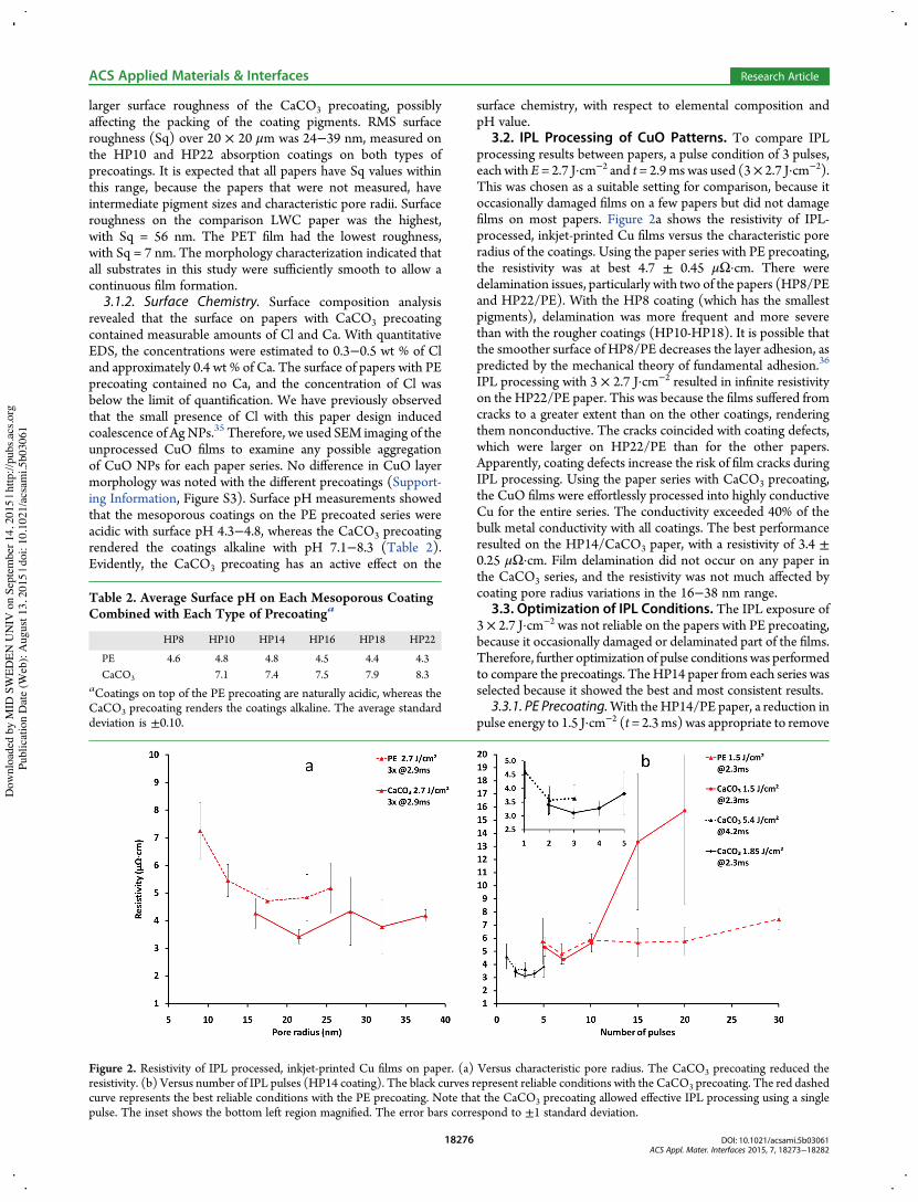
3.2. IPL Processing of CuO Patterns. To compare IPLprocessing results between papers, a pulse condition of 3 pulses,each with E = 2.7 J·cm−2 and t = 2.9 ms was used (3× 2.7 J·cm−2).This was chosen as a suitable setting for comparison, because itoccasionally damaged films on a few papers but did not damagefilms on most papers. Figure 2a shows the resistivity of IPL-processed, inkjet-printed Cu films versus the characteristic poreradius of the coatings. Using the paper series with PE precoating,the resistivity was at best 4.7 ± 0.45 μΩ·cm. There weredelamination issues, particularly with two of the papers (HP8/PEand HP22/PE). With the HP8 coating (which has the smallestpigments), delamination was more frequent and more severethan with the rougher coatings (HP10-HP18). It is possible thatthe smoother surface of HP8/PE decreases the layer adhesion, aspredicted by the mechanical theory of fundamental adhesion.36
IPL processing with 3 × 2.7 J·cm−2 resulted in infinite resistivityon the HP22/PE paper. This was because the films suffered fromcracks to a greater extent than on the other coatings, renderingthem nonconductive. The cracks coincided with coating defects,which were larger on HP22/PE than for the other papers.Apparently, coating defects increase the risk of film cracks duringIPL processing. Using the paper series with CaCO3 precoating,the CuO films were effortlessly processed into highly conductiveCu for the entire series. The conductivity exceeded 40% of thebulk metal conductivity with all coatings. The best performanceresulted on the HP14/CaCO3 paper, with a resistivity of 3.4 ±0.25 μΩ·cm. Film delamination did not occur on any paper inthe CaCO3 series, and the resistivity was not much affected bycoating pore radius variations in the 16−38 nm range.
3.3. Optimization of IPL Conditions. The IPL exposure of3 × 2.7 J·cm−2 was not reliable on the papers with PE precoating,because it occasionally damaged or delaminated part of the films.Therefore, further optimization of pulse conditions was performedto compare the precoatings. TheHP14 paper from each series wasselected because it showed the best and most consistent results.
3.3.1. PE Precoating.With theHP14/PE paper, a reduction inpulse energy to 1.5 J·cm−2 (t = 2.3ms) was appropriate to remove
Table 2. Average Surface pH on Each Mesoporous CoatingCombined with Each Type of Precoatinga
HP8 HP10 HP14 HP16 HP18 HP22
PE 4.6 4.8 4.8 4.5 4.4 4.3CaCO3 7.1 7.4 7.5 7.9 8.3
aCoatings on top of the PE precoating are naturally acidic, whereas theCaCO3 precoating renders the coatings alkaline. The average standarddeviation is ±0.10.
Figure 2. Resistivity of IPL processed, inkjet-printed Cu films on paper. (a) Versus characteristic pore radius. The CaCO3 precoating reduced theresistivity. (b) Versus number of IPL pulses (HP14 coating). The black curves represent reliable conditions with the CaCO3 precoating. The red dashedcurve represents the best reliable conditions with the PE precoating. Note that the CaCO3 precoating allowed effective IPL processing using a singlepulse. The inset shows the bottom left region magnified. The error bars correspond to ±1 standard deviation.
ACS Applied Materials & Interfaces Research Article
DOI: 10.1021/acsami.5b03061ACS Appl. Mater. Interfaces 2015, 7, 18273−18282
18276
Dow
nloa
ded
by M
ID S
WED
EN U
NIV
on
Sept
embe
r 14,
201
5 | h
ttp://
pubs
.acs
.org
P
ublic
atio
n D
ate
(Web
): A
ugus
t 13,
201
5 | d
oi: 1
0.10
21/a
csam
i.5b0
3061

all delamination tendencies. Figure 2b shows the resistivity ofCu films versus the number of IPL pulses. At 1.5 J·cm−2, at least5 pulses were required to reduce the CuO film into conductiveCu, resulting in a resistivity of 5.7 ± 1.7 μΩ·cm. Using 7 pulseswas most effective, minimizing the resistivity to 4.7± 0.8 μΩ·cm.Using more than 7 pulses, the resistivity increased, althoughit remained low and fairly constant until above 20 pulses, whencracks in the films appeared and increased the resistivityfurther (Figure 2b, dashed). No reoxidation was noticed on theHP14/PE paper.3.3.2. CaCO3 Precoating. Also, at the fairly low pulse energy
of 1.5 J·cm−2 (2.3 ms), the CaCO3 precoating lowered thefilm resistivity and its variations. Similar to the PE variant, thereduction threshold on HP14/CaCO3 was 5 pulses at 1.5 J·cm−2,and the minimum resistivity (4.4± 0.7 μΩ·cm) was reached with7 pulses. However, using 10 pulses or more, the films startedto reoxidize, greatly increasing average resistivity and resistivityvariations (Figure 2b, red, solid). With the CaCO3 precoating,pulse energies could be reliably increased, reducing resistivityfurther. All tested pulse settings, including the maximum outputcapability of 5.4 J·cm−2 (4.2 ms), were usable without delamina-tion. The most effective pulse condition was 2−4 pulses of1.85 J·cm−2 (2.3 ms), allowing consistent results around3.4 μΩ·cm (Figure 2b, black, solid). Minimum resistivity wasachieved using 3 pulses of 1.85 J·cm−2 (2.3 ms), resulting in aresistivity as low as 3.1 ± 0.2 μΩ·cm. This corresponds to morethan half of the conductivity of bulk copper, which is higherthan has been previously reported for IPL-processed Cu films.Figure 3 shows SEM images of inkjet-printed CuO films, beforeand after IPL processing using both type of precoatings. Thecross section in Figure 3d shows that the CuO film did not mixinto the coating, because the coating pore size was sufficientlysmall to prevent CuO NP intrusion. The broad CuO NP sizedistribution of approximately 10−300 nm is arguably beneficialfor the dense packing of the CuO NP film. Note that the IPLconversion to Cu increased the material density and reduced thefilm thickness significantly. The largest densification resultedwith the CaCO3 precoating (Figure 3f). Thus, for equal IPL
exposure, using the CaCO3 precoating resulted in increasedmicrostructure size, higher density and higher conductivity.A complete predrying of the substrate was observed to be
beneficial for the IPL process. If the IPL exposure vaporizesany remaining water or additives, the induced pressure gradientmay damage or delaminate the film. We observed that theCaCO3 precoating significantly reduced the need for predrying.Therefore, we postulate that the main factor explaining theenhanced IPL processing using the CaCO3 precoating is the highporosity of the precoating, allowing water and ink additives toquickly pass through it. In contrast, the PE precoating acts as abarrier, keeping water and additives directly underneath the CuOfilm. Note that even with a complete predrying, nonporoussubstrates or barriers trap nonvolatile ink additives within orbelow the film, likely damaging the film during the IPL process.
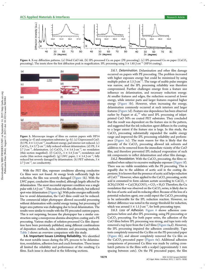
3.4. X-ray Diffraction. Figure 4 shows X-ray diffractionpatterns for dried CuO ink, IPL-processed Cu on PE-precoatedpaper and IPL-processed Cu on CaCO3-precoated paper. Theoverview scans show that the patterns are dominated by thephases CuO and Cu, respectively. The diffuse backgroundincreasing toward the low-angle side is due to the Si sampleholder. The first diffraction peak in CuO is rather broad. If weassume a shape factor of 0.9, and that all line broadening is due toa finite size of the crystallites, the Scherrer equation estimates theaverage crystallite size to approximately 12 nm. This iscomparable with the smallest CuO NPs that was observedusing TEM imaging, indicating a reasonable estimate. The firstdiffraction peak from the Cu, processed on PE-precoated paper,is significantly sharper. Crystallite size estimation using theScherrer equation yields an average of approximately 28 nm. TheCu processed on CaCO3-precoated paper shows a yet sharperpeak, indicating an average crystallite size of 36 nm. This isconsistent with the SEM images, indicating that the CaCO3precoating favors a more effective IPL material conversion.
3.5. IPL Processing Results on the ComparisonSubstrates. Figure 5 shows microscope images of films onvarious substrates, after different IPL processing conditions.
Figure 3. SEM images of inkjet-printed CuO film on paper, before and after IPL processing using 3× 1.85 J·cm−2 andHP14 coating. Top of films shownin (a−c) and corresponding cross sections shown in (d−f). Using the CaCO3 precoating enhances the effect of the processing, resulting in increasedmicrostructure size, higher density and higher conductivity. (a,d) Unprocessed CuO. (b,e) IPL-processed Cu (PE precoating). Note that the film hasdelaminated from the coating. (c,f) IPL-processed Cu (CaCO3 precoating).
ACS Applied Materials & Interfaces Research Article
DOI: 10.1021/acsami.5b03061ACS Appl. Mater. Interfaces 2015, 7, 18273−18282
18277
Dow
nloa
ded
by M
ID S
WED
EN U
NIV
on
Sept
embe
r 14,
201
5 | h
ttp://
pubs
.acs
.org
P
ublic
atio
n D
ate
(Web
): A
ugus
t 13,
201
5 | d
oi: 1
0.10
21/a
csam
i.5b0
3061
With the PET film, exposure conditions allowing conductiveCu films were not found. At energy levels sufficiently high forreduction, the film was severely damaged (Figure 5h). With theLWC paper, conductive films resulted, although largely affected bydelamination. The most successful exposure condition was a singlepulse with 5.4 J·cm−2. This reduced the film effectively, but inflictedspot-wise delamination (Figure 5g).With pulse energies sufficientlylow to avoid delamination, the CuO films could not be reduced.The commercial inkjet photopaper allowed successful processingwithout delamination with careful energy tuning, but processing oflarger-area patterns was challenging due to local delamination. Theresults were similar to results with the PE-precoated custom papers.This is not surprising, because the photopaper has a similar con-struction using a mesoporous alumina absorption coating and a PEprecoating. Various studies of solution-processed Cu film deposi-tion have been previously published, using different combinationsof deposition methods, inks, substrates and processing methods.Table 3 shows an overview comparison with this study.3.6. Important Issues Limiting Reliability. We identified
the most notable issues during the IPL process to be delamina-tion, reoxidation, adhesion loss and crack formation. These issuesall limited the reliability and performance of the resulting Cufilms. Each issue is described in the following sections.
3.6.1. Delamination. Delamination and other film damageoccurred on papers with PE precoating. The problem increasedwith higher exposure energy but could be minimized by usingmultiple pulses at 1.5 J·cm−2. The range of usable pulse energieswas narrow, and the IPL processing reliability was thereforecompromised. Further challenges emerge from a feature sizeinfluence on delamination, and necessary reduction energy.At smaller features and edges, the reduction occurred at lowerenergy, while interior parts and larger features required higherenergy (Figure 5b). However, when increasing the energy,delamination commonly occurred at such interiors and largerfeatures (Figure 5d). Feature-size dependence has been observedearlier by Paquet et al.,28 who used IPL processing of inkjet-printed CuO NPs on coated PET substrates. They concludedthat the result was dependent on the feature size in the pattern,and suggested that the ink reduction agent diffuses in the coatingto a larger extent if the feature size is large. In this study, theCaCO3 precoating substantially expanded the usable energyrange and improved the IPL processing reliability and perform-ance (Figure 5c). The main reason for this is likely that theporosity of the CaCO3 precoating allowed ink solvents andadditives to be removed from the immediate vicinity of the CuOfilm, and therefore prevented IPL-induced evaporation of suchink components to inflict delamination and other film damage.
3.6.2. Reoxidation.With the CaCO3 precoating, the films re-oxidized when subject to excessive multipulse exposure (Figure 5f).There was no visible reoxidation with the PE precoating. This isarguably due to the addition of acetic acid in the coating dis-persions. It is known that the presence of acetic acid helps reductionof CuO.39 However, when applied to the CaCO3 precoating, aceticacid is consumed to form calcium acetate according to CaCO3 +2CH3COOH→Ca(CH3COO)2 +CO2+H2O.Therefore, theCureoxidation that was observed on the CaCO3 series, is likely due tothe loss of acetic acid and its reducing effect. Because of the loss of apotential reduction agent, one could expect the CaCO3 precoatingto be unfavorable for the IPL reduction reaction. However, nodistinct difference was noted in the energy threshold for reduction,which was around 5 × 1.5 J·cm−2, for both precoating types.
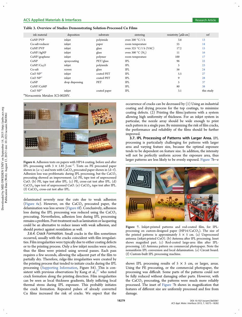
3.6.3. Loss of Adhesion. Figure 6 shows adhesion com-parisons before and after IPL processing, using PE precoating orCaCO3 precoating. For both paper series, the adhesion of theCuO films before IPL processing was strong, and tape tests onlyremoved a top layer from the CuO films (Figure 6a,d). However,the IPL processing impaired the adhesion considerably. Tapetests completely removed the Cu film on the PE-precoated paper(Figure 6b), and almost completely removed the Cu film onthe CaCO3-precoated paper (Figure 6e). Additional adhesioncomparisons of processed Cu films was made by cutting cross-hatch patterns in the films with a scalpel (approximately 1 mmspacing between cuts). On the PE precoated paper, the film
Figure 5. Microscope images of films on custom papers with HP14coating (a−f) and comparison substrates (g−h). (a) Unprocessed CuO.(b) PE, 4 × 1.5 J·cm−2, insufficient energy, pad interior not reduced. (c)CaCO3, 3 × 2.7 J·cm−2, fully reduced without delamination. (d) PE, 3 ×2.7 J·cm−2, delamination. (e) CaCO3, 3 × 5.4 J·cm−2, no reoxidation(thin section magnified). (f) CaCO3, 5 × 5.4 J·cm−2, reoxidation andcracks (thin section magnified). (g) LWC paper, 1 × 5.4 J·cm−2, fullyreduced but severely damaged by delamination. (h) PET substrate, 3 ×2.7 J·cm−2, no conductivity.
Figure 4. X-ray diffraction patterns. (a) Dried CuO ink. (b) IPL-processed Cu on paper (PE precoating). (c) IPL-processed Cu on paper (CaCO3precoating). The insets show the first diffraction peak in magnification. IPL processing using 3 × 1.85 J·cm−2 (HP14 coating).
ACS Applied Materials & Interfaces Research Article
DOI: 10.1021/acsami.5b03061ACS Appl. Mater. Interfaces 2015, 7, 18273−18282
18278
Dow
nloa
ded
by M
ID S
WED
EN U
NIV
on
Sept
embe
r 14,
201
5 | h
ttp://
pubs
.acs
.org
P
ublic
atio
n D
ate
(Web
): A
ugus
t 13,
201
5 | d
oi: 1
0.10
21/a
csam
i.5b0
3061
delaminated severely near the cuts due to weak adhesion(Figure 6c). However, on the CaCO3 precoated paper, thedelamination was less severe (Figure 6f). Conclusively, adhesionloss during the IPL processing was reduced using the CaCO3precoating. Nevertheless, adhesion loss during IPL processingremains a problem. Post-treatment such as lamination or lacqueringcould be an alternative to reduce issues with weak adhesion, andshould protect against reoxidation as well.3.6.4. Crack Formation. Small cracks in the film sometimes
occurred, usually with the cracks coincident with film irregulari-ties. Film irregularities were typically due to either coating defectsor to the printing process. Only a few inkjet nozzles were active,thus the films were printed using several passes. Each passrequires a few seconds, allowing the adjacent part of the film topartially dry. Therefore, ridge-like irregularities were created bythe printing process that tended to initiate cracks during the IPLprocessing (Supporting Information, Figure S4). This is con-sistent with previous observations by Kang et al.,27 who notedcrack formation along the printing direction. Film irregularitiescan be seen as local thickness gradients, likely inflicting localthermal stress during IPL exposure. This probably initiatesthe crack formation. Repeated pulses of already convertedCu films increased the risk of cracks. We expect that the
occurrence of cracks can be decreased by (1) Using an industrialcoating and drying process for the top coatings, to minimizecoating defects. (2) Printing the films/patterns with a systemallowing high uniformity of thickness. For an inkjet system inparticular, the nozzle array should be wide enough to printeach pattern in a single pass. By minimizing the risk of film cracks,the performance and reliability of the films should be furtherimproved.
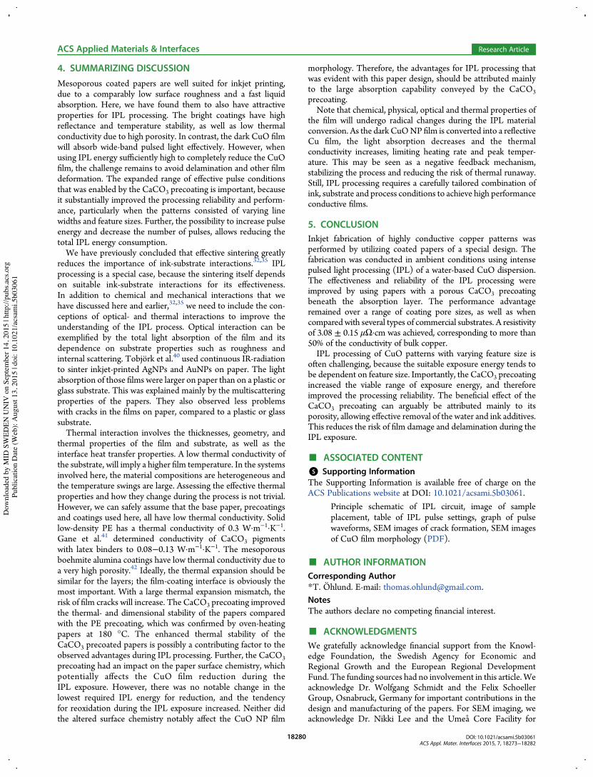
3.7. IPL Processing of Patterns with Larger Area. IPLprocessing is particularly challenging for patterns with largerarea and varying feature size, because the optimal exposuretends to be dependent on feature size. In addition, the intensitywill not be perfectly uniform across the exposure area, thuslarger patterns are less likely to be evenly exposed. Figure 7b−e
shows IPL processing results of 5 × 5 cm, or larger, areas.Using the PE precoating, or the commercial photopaper, theprocessing was difficult. Some parts of the patterns could notbe fully reduced without damaging other parts. However, withthe CaCO3 precoating, the patterns were much more reliablyprocessed. The inset of Figure 7b shows in magnification thatfeatures of different size are uniformly processed and free fromdamage.
Table 3. Overview of Studies Demonstrating Solution-Processed Cu Films
ink material deposition substrate sintering resistivity [μΩ·cm] ref
CuNP/PVP inkjet polyimide oven 200 °C/1 h 3.6 13Cu-salt+reducer inkjet paper room temperature 55 14CuNP/PVP inkjet glass oven 325 °C/1 h (VAC) 17.2 15CuNP/AgNP inkjet glass oven 300 °C (N2) 11 16CuNP/graphene inkjet polymer room temperature 100 17CuNP spraycoating PET/glass IPL 96 22CuNP/Cu2O inkjet polyimide IPL 5 23Cu-salt screen glass IPL 56 24CuO NPa inkjet coated PET IPL 5.5 27CuO NPa inkjet coated PET IPL 9 28CuNP drop dispensing PET IPL 5 37CuNP/CuMP IPL 80 38CuO NPa inkjet coated paper IPL 3.1 this study
aNovacentrix Metalon ICI-002HV.
Figure 6. Adhesion tests on papers with HP14 coating, before and afterIPL processing with 3 × 1.85 J·cm−2. Tests on PE precoated papershown in (a−c) and tests with CaCO3 precoated paper shown in (d−f).Adhesion loss was problematic during IPL processing, but the CaCO3precoating showed an improvement. (a) PE, tape test of unprocessedCuO. (b) PE, tape test after IPL. (c) PE, cross-cut test after IPL. (d)CaCO3, tape test of unprocessed CuO. (e) CaCO3, tape test after IPL.(f) CaCO3, cross-cut test after IPL.
Figure 7. Inkjet-printed patterns and rod-coated film, for IPL-processing on custom-designed paper (HP14/CaCO3). The size ofthe printed patterns is approximately 5 × 5 cm. (a) Unprocessedantenna (inkjet-printed CuO). (b) Antenna after IPL processing. Insetshows magnified part. (c) Rod-coated large-area film after IPL-processing. (d) Antenna pattern on commercial photopaper. Note thenonuniform IPL conversion and local delamination. (e) Circuit board.(f) Custom-built IPL processing machine.
ACS Applied Materials & Interfaces Research Article
DOI: 10.1021/acsami.5b03061ACS Appl. Mater. Interfaces 2015, 7, 18273−18282
18279
Dow
nloa
ded
by M
ID S
WED
EN U
NIV
on
Sept
embe
r 14,
201
5 | h
ttp://
pubs
.acs
.org
P
ublic
atio
n D
ate
(Web
): A
ugus
t 13,
201
5 | d
oi: 1
0.10
21/a
csam
i.5b0
3061
4. SUMMARIZING DISCUSSIONMesoporous coated papers are well suited for inkjet printing,due to a comparably low surface roughness and a fast liquidabsorption. Here, we have found them to also have attractiveproperties for IPL processing. The bright coatings have highreflectance and temperature stability, as well as low thermalconductivity due to high porosity. In contrast, the dark CuO filmwill absorb wide-band pulsed light effectively. However, whenusing IPL energy sufficiently high to completely reduce the CuOfilm, the challenge remains to avoid delamination and other filmdeformation. The expanded range of effective pulse conditionsthat was enabled by the CaCO3 precoating is important, becauseit substantially improved the processing reliability and perform-ance, particularly when the patterns consisted of varying linewidths and feature sizes. Further, the possibility to increase pulseenergy and decrease the number of pulses, allows reducing thetotal IPL energy consumption.We have previously concluded that effective sintering greatly
reduces the importance of ink-substrate interactions.32,35 IPLprocessing is a special case, because the sintering itself dependson suitable ink-substrate interactions for its effectiveness.In addition to chemical and mechanical interactions that wehave discussed here and earlier,32,35 we need to include the con-ceptions of optical- and thermal interactions to improve theunderstanding of the IPL process. Optical interaction can beexemplified by the total light absorption of the film and itsdependence on substrate properties such as roughness andinternal scattering. Tobjork et al.40 used continuous IR-radiationto sinter inkjet-printed AgNPs and AuNPs on paper. The lightabsorption of those films were larger on paper than on a plastic orglass substrate. This was explained mainly by the multiscatteringproperties of the papers. They also observed less problemswith cracks in the films on paper, compared to a plastic or glasssubstrate.Thermal interaction involves the thicknesses, geometry, and
thermal properties of the film and substrate, as well as theinterface heat transfer properties. A low thermal conductivity ofthe substrate, will imply a higher film temperature. In the systemsinvolved here, the material compositions are heterogeneous andthe temperature swings are large. Assessing the effective thermalproperties and how they change during the process is not trivial.However, we can safely assume that the base paper, precoatingsand coatings used here, all have low thermal conductivity. Solidlow-density PE has a thermal conductivity of 0.3 W·m−1·K−1.Gane et al.41 determined conductivity of CaCO3 pigmentswith latex binders to 0.08−0.13 W·m−1·K−1. The mesoporousboehmite alumina coatings have low thermal conductivity due toa very high porosity.42 Ideally, the thermal expansion should besimilar for the layers; the film-coating interface is obviously themost important. With a large thermal expansion mismatch, therisk of film cracks will increase. The CaCO3 precoating improvedthe thermal- and dimensional stability of the papers comparedwith the PE precoating, which was confirmed by oven-heatingpapers at 180 °C. The enhanced thermal stability of theCaCO3 precoated papers is possibly a contributing factor to theobserved advantages during IPL processing. Further, the CaCO3precoating had an impact on the paper surface chemistry, whichpotentially affects the CuO film reduction during theIPL exposure. However, there was no notable change in thelowest required IPL energy for reduction, and the tendencyfor reoxidation during the IPL exposure increased. Neither didthe altered surface chemistry notably affect the CuO NP film
morphology. Therefore, the advantages for IPL processing thatwas evident with this paper design, should be attributed mainlyto the large absorption capability conveyed by the CaCO3precoating.Note that chemical, physical, optical and thermal properties of
the film will undergo radical changes during the IPL materialconversion. As the dark CuONP film is converted into a reflectiveCu film, the light absorption decreases and the thermalconductivity increases, limiting heating rate and peak temper-ature. This may be seen as a negative feedback mechanism,stabilizing the process and reducing the risk of thermal runaway.Still, IPL processing requires a carefully tailored combination ofink, substrate and process conditions to achieve high performanceconductive films.
5. CONCLUSIONInkjet fabrication of highly conductive copper patterns wasperformed by utilizing coated papers of a special design. Thefabrication was conducted in ambient conditions using intensepulsed light processing (IPL) of a water-based CuO dispersion.The effectiveness and reliability of the IPL processing wereimproved by using papers with a porous CaCO3 precoatingbeneath the absorption layer. The performance advantageremained over a range of coating pore sizes, as well as whencompared with several types of commercial substrates. A resistivityof 3.08 ± 0.15 μΩ·cm was achieved, corresponding to more than50% of the conductivity of bulk copper.IPL processing of CuO patterns with varying feature size is
often challenging, because the suitable exposure energy tends tobe dependent on feature size. Importantly, the CaCO3 precoatingincreased the viable range of exposure energy, and thereforeimproved the processing reliability. The beneficial effect of theCaCO3 precoating can arguably be attributed mainly to itsporosity, allowing effective removal of the water and ink additives.This reduces the risk of film damage and delamination during theIPL exposure.
■ ASSOCIATED CONTENT*S Supporting InformationThe Supporting Information is available free of charge on theACS Publications website at DOI: 10.1021/acsami.5b03061.
Principle schematic of IPL circuit, image of sampleplacement, table of IPL pulse settings, graph of pulsewaveforms, SEM images of crack formation, SEM imagesof CuO film morphology (PDF).
■ AUTHOR INFORMATIONCorresponding Author*T. Ohlund. E-mail: [email protected] authors declare no competing financial interest.
■ ACKNOWLEDGMENTSWe gratefully acknowledge financial support from the Knowl-edge Foundation, the Swedish Agency for Economic andRegional Growth and the European Regional DevelopmentFund. The funding sources had no involvement in this article. Weacknowledge Dr. Wolfgang Schmidt and the Felix SchoellerGroup, Osnabruck, Germany for important contributions in thedesign and manufacturing of the papers. For SEM imaging, weacknowledge Dr. Nikki Lee and the Umea Core Facility for
ACS Applied Materials & Interfaces Research Article
DOI: 10.1021/acsami.5b03061ACS Appl. Mater. Interfaces 2015, 7, 18273−18282
18280
Dow
nloa
ded
by M
ID S
WED
EN U
NIV
on
Sept
embe
r 14,
201
5 | h
ttp://
pubs
.acs
.org
P
ublic
atio
n D
ate
(Web
): A
ugus
t 13,
201
5 | d
oi: 1
0.10
21/a
csam
i.5b0
3061

Electron Microscopy (UCEM) at Umea University. We thankProf. Magnus Norgren for valuable discussions.
■ REFERENCES(1) Sridhar, A.; van Dijk, D. J.; Akkerman, R. Inkjet Printing andAdhesion Characterisation of Conductive Tracks on a CommercialPrinted Circuit Board Material. Thin Solid Films 2009, 517, 4633−4637.(2) Shaker, G.; Safavi-Naeini, S.; Sangary, N.; Tentzeris, M. M. InkjetPrinting of Ultrawideband (UWB) Antennas on Paper-BasedSubstrates. Antenn. Wireless Propag. Lett., IEEE 2011, 10, 111−114.(3) Liana, D. D.; Raguse, B.; Gooding, J. J.; Chow, E. Recent Advancesin Paper-Based Sensors. Sensors 2012, 12, 11505−11526.(4) Sandstrom, A.; Dam, H. F.; Krebs, F. C.; Edman, L. AmbientFabrication of Flexible and Large-Area Organic Light-Emitting DevicesUsing Slot-Die Coating. Nat. Commun. 2012, 3, 1002.(5) Kang, H.; Jung, S.; Jeong, S.; Kim, G.; Lee, K. Polymer-MetalHybrid Transparent Electrodes for Flexible Electronics. Nat. Commun.2015, 6, 6503.(6) Lee, J.-Y.; Connor, S. T.; Cui, Y.; Peumans, P. Solution-ProcessedMetal Nanowire Mesh Transparent Electrodes. Nano Lett. 2008, 8,689−692.(7) Yoon, H.; Jang, J. Conducting-Polymer Nanomaterials for High-Performance Sensor Applications: Issues and Challenges. Adv. Funct.Mater. 2009, 19, 1567−1576.(8) Yoshioka, Y.; Jabbour, G. E. Desktop Inkjet Printer as a Tool toPrint Conducting Polymers. Synth. Met. 2006, 156, 779−783.(9) Sirringhaus, H.; Kawase, T.; Friend, R. H.; Shimoda, T.;Inbasekaran, M.; Wu, W.; Woo, E. P. High-Resolution Inkjet Printingof All-Polymer Transistor Circuits. Science 2000, 290, 2123−2126.(10) Kordas, K.; Mustonen, T.; Toth, G.; Jantunen, H.; Lajunen, M.;Soldano, C.; Talapatra, S.; Kar, S.; Vajtai, R.; Ajayan, P. M. InkjetPrinting of Electrically Conductive Patterns of Carbon Nanotubes.Small 2006, 2, 1021−1025.(11) Huang, L.; Huang, Y.; Liang, J.; Wan, X.; Chen, Y. Graphene-Based Conducting Inks for Direct Inkjet Printing of Flexible ConductivePatterns and their Applications in Electric Circuits and ChemicalSensors. Nano Res. 2011, 4, 675−684.(12) Li, Y.; Wu, Y.; Ong, B. S. Facile Synthesis of Silver NanoparticlesUseful for Fabrication of High-Conductivity Elements for PrintedElectronics. J. Am. Chem. Soc. 2005, 127, 3266−3267.(13) Lee, Y.; Choi, J.-r.; Lee, K. J.; Stott, N. E.; Kim, D. Large-ScaleSynthesis of Copper Nanoparticles by Chemically ControlledReduction for Applications of Inkjet-Printed Electronics. Nano-technology 2008, 19, 415604.(14) Li, D.; Sutton, D.; Burgess, A.; Graham, D.; Calvert, P. D.Conductive Copper and Nickel Lines via Reactive Inkjet Printing. J.Mater. Chem. 2009, 19, 3719−3724.(15) Park, B. K.; Kim, D.; Jeong, S.; Moon, J.; Kim, J. S. Direct Writingof Copper Conductive Patterns by Ink-Jet Printing. Thin Solid Films2007, 515, 7706−7711.(16) Grouchko, M.; Kamyshny, A.; Magdassi, S. Formation of Air-Stable Copper-Silver Core-Shell Nanoparticles for Inkjet Printing. J.Mater. Chem. 2009, 19, 3057−3062.(17) Luechinger, N. A.; Athanassiou, E. K.; Stark, W. J. Graphene-Stabilized Copper Nanoparticles as an Air-Stable Substitute for Silverand Gold in Low-Cost Ink-Jet Printable Electronics. Nanotechnology2008, 19, 445201.(18) Jang, S.; Seo, Y.; Choi, J.; Kim, T.; Cho, J.; Kim, S.; Kim, D.Sintering of Inkjet Printed Copper Nanoparticles for FlexibleElectronics. Scr. Mater. 2010, 62, 258−261.(19) Kamyshny, A. Metal-Based Inkjet Inks for Printed Electronics.Open Appl. Phys. J. 2011, 4, 19−36.(20) Haynes, W. M. CRC Handbook of Chemistry and Physics, 93rd ed;CRC Press: Boca Raton, FL, 2012.(21) Farnsworth, S.; Schroder, K.; Wenz, B.; Pope, D.; Rawson, I. 32.4:Invited Paper: Broad Implications Arising from Photonic CuringProcess For Printed Electronics and Displays. Dig. Tech. Pap. - Soc. Inf.Disp. Int. Symp. 2012, 43, 430−433.
(22) Dharmadasa, R.; Jha, M.; Amos, D. A.; Druffel, T. RoomTemperature Synthesis of a Copper Ink for the Intense Pulsed LightSintering of Conductive Copper Films.ACSAppl. Mater. Interfaces 2013,5, 13227−13234.(23) Ryu, J.; Kim, H.-S.; Hahn, H. T. Reactive Sintering of CopperNanoparticles Using Intense Pulsed Light for Printed Electronics. J.Electron. Mater. 2011, 40, 42−50.(24) Araki, T.; Sugahara, T.; Jiu, J.; Nagao, S.; Nogi, M.; Koga, H.;Uchida, H.; Shinozaki, K.; Suganuma, K. Cu Salt Ink Formulation forPrinted Electronics using Photonic Sintering. Langmuir 2013, 29,11192−11197.(25) Hwang, H.-J.; Chung, W.-H.; Kim, H.-S. In Situ Monitoring ofFlash-Light Sintering of Copper Nanoparticle Ink for PrintedElectronics. Nanotechnology 2012, 23, 485205.(26) Chung, W.-H.; Hwang, H.-J.; Kim, H.-S. Flash Light SinteredCopper Precursor/Nanoparticle Pattern with High Electrical Con-ductivity and Low Porosity for Printed Electronics. Thin Solid Films2015, 580, 61−70.(27) Kang, H.; Sowade, E.; Baumann, R. R. Direct Intense Pulsed LightSintering of Inkjet-Printed Copper Oxide Layers within Six Milli-seconds. ACS Appl. Mater. Interfaces 2014, 6, 1682−1687.(28) Paquet, C.; James, R.; Kell, A. J.; Mozenson, O.; Ferrigno, J.;Lafreniere, S.; Malenfant, P. R. L. Photosintering and ElectricalPerformance of CuO Nanoparticle Inks. Org. Electron. 2014, 15,1836−1842.(29) Novacentrix Home Page. https://www.novacentrix.com (ac-cessed June 17, 2015).(30) Kipphan, H.Handbook of Print Media: Technologies and ProductionMethods, 2001 ed; Springer-Verlag: Berlin, Germany, 2001.(31) Ohlund, T.; Andersson, M. Effect of Paper Properties onElectrical Conductivity and Pattern Definition for Silver NanoparticleInkjet Ink. Proceedings of LOPE-C 2012, Munich, Germany, June 19−21,2012; pp 115−119.(32) Ohlund, T.; Ortegren, J.; Forsberg, S.; Nilsson, H.-E. PaperSurfaces for Metal Nanoparticle Inkjet Printing. Appl. Surf. Sci. 2012,259, 731−739.(33) Bollstrom, R.; Maattanen, A.; Tobjork, D.; Ihalainen, P.;Kaihovirta, N.; Osterbacka, R.; Peltonen, J.; Toivakka, M. A MultilayerCoated Fiber-Based Substrate Suitable for Printed Functionality. Org.Electron. 2009, 10, 1020−1023.(34) Hsieh, M.-C.; Kim, C.; Nogi, M.; Suganuma, K. ElectricallyConductive Lines on Cellulose Nanopaper for Flexible ElectricalDevices. Nanoscale 2013, 5, 9289−9295.(35) Ohlund, T.; Schuppert, A.; Andres, B.; Andersson, H.; Forsberg,S.; Schmidt, W.; Nilsson, H.-E.; Andersson, M.; Zhang, R.; Olin, H.Assisted Sintering of Silver Nanoparticle Inkjet Ink on Paper with ActiveCoatings. RSC Adv. 2015, 5, 64841−64849.(36) Packham, D. Theories of Fundamental Adhesion. InHandbook ofAdhesion Technology; da Silva, L. M.; Ochsner, A.; Adams, R., Eds.;Springer: Berlin, Heidelberg, 2011; Chapter 2, pp 9−38.(37) Kim, H.-S.; Dhage, S.; Shim, D.-E.; Hahn, H. T. Intense PulsedLight Sintering of Copper Nanoink for Printed Electronics. Appl. Phys.A: Mater. Sci. Process. 2009, 97, 791−798.(38) Joo, S.-J.; Hwang, H.-J.; Kim, H.-S. Highly Conductive CopperNano/Microparticles Ink via Flash Light Sintering for PrintedElectronics. Nanotechnology 2014, 25, 265601.(39) Kim, I.; Joung, J. W.; SONG, Y. A. Reducing Agent for LowTemperature Reducing and Sintering of Copper Nanoparticles, andMethod for Low Temperature Sintering Using the Same. Patent US20100055302, March 4, 2010.(40) Tobjork, D.; Aarnio, H.; Pulkkinen, P.; Bollstrom, R.; Maattanen,A.; Ihalainen, P.; Makela, T.; Peltonen, J.; Toivakka, M.; Tenhu, H.;Osterbacka, R. IR-Sintering of Ink-Jet Printed Metal-Nanoparticles onPaper. Thin Solid Films 2012, 520, 2949−2955.(41) Gane, P.; Ridgway, C.; Schoelkopf, J.; Bousfield, D. Heat Transferthrough Calcium Carbonate-Based Coating Structures: Observationand Model for a Thermal Fusing Process. J. Pulp Pap. Sci. 2007, 33, 60−70.
ACS Applied Materials & Interfaces Research Article
DOI: 10.1021/acsami.5b03061ACS Appl. Mater. Interfaces 2015, 7, 18273−18282
18281
Dow
nloa
ded
by M
ID S
WED
EN U
NIV
on
Sept
embe
r 14,
201
5 | h
ttp://
pubs
.acs
.org
P
ublic
atio
n D
ate
(Web
): A
ugus
t 13,
201
5 | d
oi: 1
0.10
21/a
csam
i.5b0
3061
(42) Ha, T.-J.; Park, H.-H.; Kang, E. S.; Shin, S.; Cho, H. H. Variationsin Mechanical and Thermal Properties of Mesoporous Alumina ThinFilms due to Porosity andOrdered Pore Structure. J. Colloid Interface Sci.2010, 345, 120−124.
ACS Applied Materials & Interfaces Research Article
DOI: 10.1021/acsami.5b03061ACS Appl. Mater. Interfaces 2015, 7, 18273−18282
18282
Dow
nloa
ded
by M
ID S
WED
EN U
NIV
on
Sept
embe
r 14,
201
5 | h
ttp://
pubs
.acs
.org
P
ublic
atio
n D
ate
(Web
): A
ugus
t 13,
201
5 | d
oi: 1
0.10
21/a
csam
i.5b0
3061


