Ink Jet Printing and Spin-coating of Electrically ... · Peter C. Wilson, Constantina Lekakou, John...
29
Peter C. Wilson, Constantina Lekakou, John F. Watts Ink Jet Printing and Spin-coating of Electrically Conductive Polymers Presentation Outline • PhD Outline • Background • Custom Ink Jet Printing Equipment • Electro-impedance Model • Charge Transport Method • Microscale Comparison • Mobility & Morphology • Ongoing & Future Work
-
Upload
truongtruc -
Category
Documents
-
view
223 -
download
0
Transcript of Ink Jet Printing and Spin-coating of Electrically ... · Peter C. Wilson, Constantina Lekakou, John...

Peter C. Wilson, Constantina Lekakou, John F. Watts
Ink Jet Printing and Spin-coating
of Electrically Conductive Polymers
Presentation Outline
• PhD Outline
• Background
• Custom Ink Jet Printing Equipment
• Electro-impedance Model
• Charge Transport Method
• Microscale Comparison
• Mobility & Morphology
• Ongoing & Future Work

Peter C. Wilson, Constantina Lekakou, John F. Watts
Ink Jet Printing and Spin-coating
of Electrically Conductive Polymers
PEDOT Useage
Simple organic device structure displaying PEDOT:PSS as a
high work function anode
Figure 8 - Comparative assessment of
PEDOT:PSS films compared to ITO
layers.
Device life-time is omitted ~ 7x ITO

Peter C. Wilson, Constantina Lekakou, John F. Watts
Ink Jet Printing and Spin-coating
of Electrically Conductive Polymers
Gas Line
Motors
Control Cards
JetServer
Camera
Reservoir
Heat Pad
Substrate Temp Control
Jetter
Strobe
Control Program
Monitor
Inkjet Printer Setup

Peter C. Wilson, Constantina Lekakou, John F. Watts
Ink Jet Printing and Spin-coating
of Electrically Conductive Polymers
InkJet Printer OverviewControllable Parameters
• Drop size
• Ejection wave guide architecture
• Drop velocity
• Drop / substrate Temperature
• Drop placing / overlap
• Print rate
• Print layering
• Ejection angle
• Drop chemistry
Rig Specification
250dpi @ Ts = 50deg C
Position accuracy < 2μm (at 1/8th step)
Position repeatability < 10 μm
Print rate from 0 – 100mm s-1
Print acceleration 0 – 100m s-2Transmission Optical Microscopy Of
Printed PEDOT:PSS Tracks - 100um orifice jetter, 5% drop overlap

Peter C. Wilson, Constantina Lekakou, John F. Watts
Ink Jet Printing and Spin-coating
of Electrically Conductive Polymers
PEDOT:PSS Surface Tension As A Function Of DMSO DMSO & Surfynol 2502
Concentration
0
0.01
0.02
0.03
0.04
0.05
0.06
0.07
0.08
0 1 2 3 4 5 6
DMSO %wt
Surf
ace T
ensio
n (
N/m
)
0% Surfynol
1% Surfynol
Linear (0% Surfynol)

Peter C. Wilson, Constantina Lekakou, John F. Watts
Ink Jet Printing and Spin-coating
of Electrically Conductive Polymers
Electro-impedance Spectroscopy
Nyquist plot for Inkjet Printed PEDOT:PSS (5%wt DMSO, 0%Surfynol) at 93K

Peter C. Wilson, Constantina Lekakou, John F. Watts
Ink Jet Printing and Spin-coating
of Electrically Conductive Polymers
Electro-impedance Spectroscopy
|REL| Bode plot for Inkjet Printed PEDOT:PSS (5%wt DMSO, 0%Surfynol) at 93K

Peter C. Wilson, Constantina Lekakou, John F. Watts
Ink Jet Printing and Spin-coating
of Electrically Conductive Polymers
Electro-impedance Spectroscopy
Zplot model fitting for Inkjet Printed PEDOT:PSS (5%wt DMSO, 0%Surfynol) at 93K

Peter C. Wilson, Constantina Lekakou, John F. Watts
Ink Jet Printing and Spin-coating
of Electrically Conductive Polymers
Electro-impedance Spectroscopy
Zplot equivalent circuitry for Inkjet Printed PEDOT:PSS (5%wt DMSO, 0%Surfynol) at 93K
Series Resistance
Surface capacitive region
Bulk PEDOT:PSS film

Peter C. Wilson, Constantina Lekakou, John F. Watts
Ink Jet Printing and Spin-coating
of Electrically Conductive Polymers
Surface Resistivity For 0-1% Surfynol, 0-5% DMSO InkJet Printed Films
1.00E+02
1.00E+03
1.00E+04
1.00E+05
1.00E+06
1.00E+07
0 1 2 3 4 5
DMSO %wt
Res
isti
vit
y W
/sq
Surface Resistivity (0%wt Surfynol)
Surface Resistivity (1%wt Surfynol)

Peter C. Wilson, Constantina Lekakou, John F. Watts
Ink Jet Printing and Spin-coating
of Electrically Conductive Polymers
4-Point Hall Probe demonstrate the effect on carrier mobility in inkjet printed PEDOT:PSS thin films
• 0% DMSO, 1% Surfynol,
•
• 1.164x 10⁵ W sq-1 ~ 11 W cm-1 (0.09 S cm-1)
• Carrier Mobility 1.43 cm-2 v-1s-1
• Carrier Concentration ~ 3.74 x1013 cm-2
• 5% DMSO, 1% Surfynol,
• 633 W sq-1 ~ 6.33 x10⁻² W cm-1 (16 S cm-1)
• Carrier Mobility 397 cm-2 v-1s-1
• Carrier Concentration ~ 2.48 x1013 cm-2
Printed samples displayed ohmic contacts and excellent film uniformity

Peter C. Wilson, Constantina Lekakou, John F. Watts
Ink Jet Printing and Spin-coating
of Electrically Conductive Polymers
Surface Resistivity For 0-1% Surfynol, 0-5% DMSO Spin Coated Films
1.00E+03
1.00E+04
1.00E+05
1.00E+06
1.00E+07
1.00E+08
0 1 2 3 4 5
DMSO %wt
Re
sist
ivit
y W
/sq
Surface Resistivity (0% Surfynol)
Surface Resistivity (1% Surfynol)

Peter C. Wilson, Constantina Lekakou, John F. Watts
Ink Jet Printing and Spin-coating
of Electrically Conductive Polymers
x
e

Peter C. Wilson, Constantina Lekakou, John F. Watts
Ink Jet Printing and Spin-coating
of Electrically Conductive Polymers
T
TEXP 0
0
Mott Variable Range Hopping Law,
denote the recipical dimensionality of conduction
the conductivity
o & T0 are material constants

Peter C. Wilson, Constantina Lekakou, John F. Watts
Ink Jet Printing and Spin-coating
of Electrically Conductive Polymers
Reproduced from - A. M. Nardes, M. Kemerink, R. A. J. Janssen,
“Anisotropic hopping conduction in spin coated PEDOT:PSS thin films”,
Phys. Rev. B 2007, 76, 085208-1.
Charge transport asymmetry in spin coated
PEDOT:PSS films due to oblate spheroid-type
conducting grain morphology
- 3d variable range hopping in the parallel plane
- Space Charge limited tunnelling in the normal plane
Peter C. Wilson, Constantina Lekakou, John F. Watts
Ink Jet Printing and Spin-coating
of Electrically Conductive Polymers
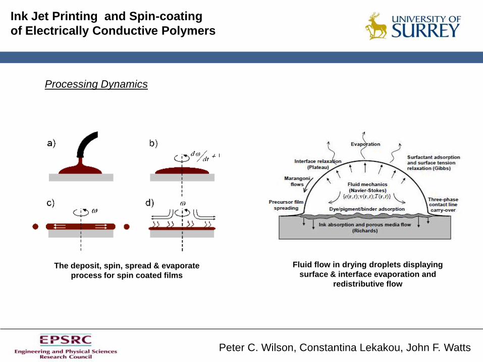
Processing Dynamics
The deposit, spin, spread & evaporate
process for spin coated films
Fluid flow in drying droplets displaying
surface & interface evaporation and
redistributive flow

Peter C. Wilson, Constantina Lekakou, John F. Watts
Ink Jet Printing and Spin-coating
of Electrically Conductive Polymers
Parallel plane conductivity displaying Nearest Neighbour Hopping (nn-H)
conduction mode.

Peter C. Wilson, Constantina Lekakou, John F. Watts
Ink Jet Printing and Spin-coating
of Electrically Conductive Polymers
R² = 0.9855
0.001
0.01
0.1
0.25 0.26 0.27 0.28 0.29 0.3 0.31
D
C (
S/cm
)
T-0.25 (K-0.25)
(DC) As A Function Of Temperature For InkJet PEDOT:PSS (4%wt DMSO) - Fitting T-0.25
Parallel plane conductivity displaying 3d Variable Range Hopping
behaviour

Peter C. Wilson, Constantina Lekakou, John F. Watts
Ink Jet Printing and Spin-coating
of Electrically Conductive Polymers
Drop Observation
303K
323K
353K
SEM Images For Identical Inks At 3 Substrate Temperatures

Peter C. Wilson, Constantina Lekakou, John F. Watts
Ink Jet Printing and Spin-coating
of Electrically Conductive Polymers
Drop Profilometry
303K
323K
353K
Single Drop Profilometry For Identical Inks At 3 Substrate Temperatures

Peter C. Wilson, Constantina Lekakou, John F. Watts
Ink Jet Printing and Spin-coating
of Electrically Conductive Polymers
Drop Profile As A Function Of Substrate Temperature
-0.05
0.05
0.15
0.25
0.35
0.45
0 20 40 60 80 100 120 140 160 180 200
Displacment (mm)
Hei
gh
t ( m
m)
Ts = 30
Ts = 40
Ts = 50
Ts = 60
Ts = 70
Drop Shape Evolution For Identical InkJet Printed PEDOT:PSS Drops At Varying Substrate Temperatures

Peter C. Wilson, Constantina Lekakou, John F. Watts
Ink Jet Printing and Spin-coating
of Electrically Conductive Polymers
Droplet Diameter As A Function Of Substrate To Liquid
Temperature Ratio
0
20
40
60
80
100
120
140
160
180
303 313 323 333 343
Substrate Temperature (K)
Dro
ple
t D
iam
ete
r (u
m)
0.9
0.95
1
1.05
1.1
1.15
1.2
Sub
stra
te T
o L
iqu
id
Te
mp
era
ture
Rat
io
Droplet Diameter
Liquid To Substrate
Temperature Ratio

Peter C. Wilson, Constantina Lekakou, John F. Watts
Ink Jet Printing and Spin-coating
of Electrically Conductive Polymers
Peak To Trough Ratio As A Function Of Substrate To Liquid
Temperature Ratio
0
1
2
3
4
5
6
7
8
303 313 323 333 343
Substrate Temperature (K)
Pe
ak T
o T
rou
gh
Rat
io
0.9
0.95
1
1.05
1.1
1.15
1.2
Sub
stra
te T
o L
iqu
id
Te
mp
era
ture
Rat
io
Peak To Trough Ratio
Liquid To Substrate
Temperature Ratio

Peter C. Wilson, Constantina Lekakou, John F. Watts
Ink Jet Printing and Spin-coating
of Electrically Conductive Polymers
Electrostatic Force Microscopy
Electrostatic Force Microscopy (EFM) Displaying sub-surface concentric ring charge
concentration in InkJet Printed PEDOT:PSS films
AFM Phase AFM TopographyEFM Phase
Peter C. Wilson, Constantina Lekakou, John F. Watts
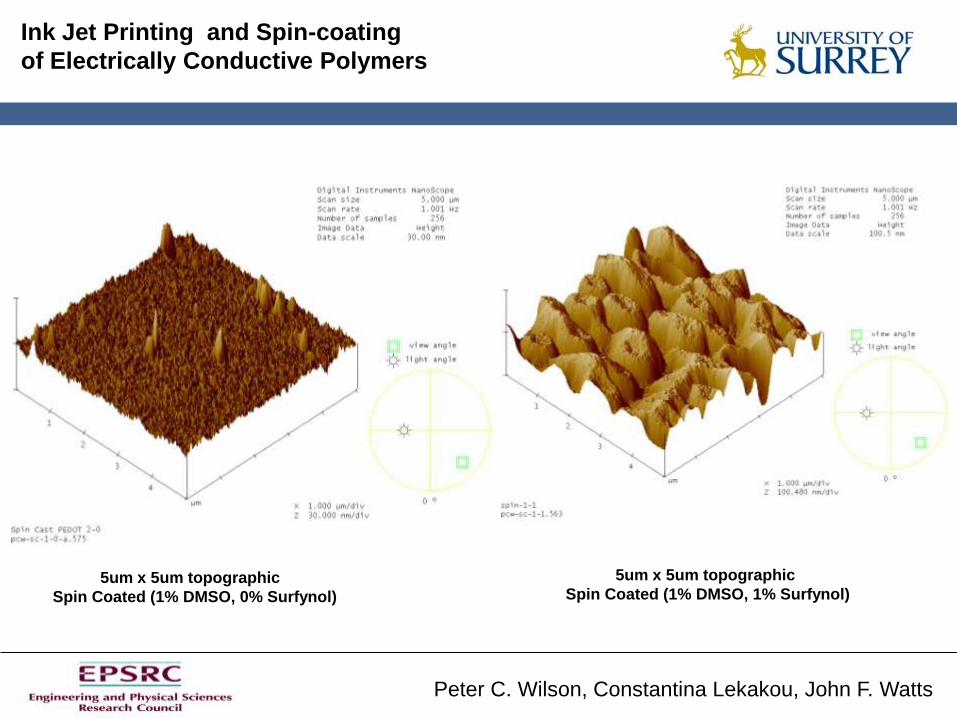
Ink Jet Printing and Spin-coating
of Electrically Conductive Polymers
5um x 5um topographic
Spin Coated (1% DMSO, 0% Surfynol)
5um x 5um topographic
Spin Coated (1% DMSO, 1% Surfynol)

Peter C. Wilson, Constantina Lekakou, John F. Watts
Ink Jet Printing and Spin-coating
of Electrically Conductive Polymers
2um x 2um topographic
InkJet (1% DMSO, 0%Surfynol)
2um x 2um topographic
InkJet (1% DMSO, 1%Surfynol)
Peter C. Wilson, Constantina Lekakou, John F. Watts
Ink Jet Printing and Spin-coating
of Electrically Conductive Polymers
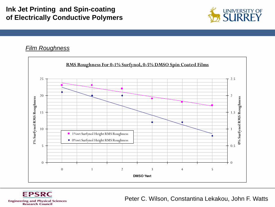
Film Roughness
RMS Roughness For 0-1% Surfynol, 0-5% DMSO Spin Coated Films
0
5
10
15
20
25
0 1 2 3 4 5
DMSO %wt
1% S
urf
yn
ol
RM
S R
ou
gh
ne
ss
0
0.5
1
1.5
2
2.5
0% S
urf
yn
ol
RM
S R
ou
gh
ne
ss
1%wt Surfynol Height RMS Roughness
0%wt Surfynol Height RMS Roughness

Peter C. Wilson, Constantina Lekakou, John F. Watts
Ink Jet Printing and Spin-coating
of Electrically Conductive Polymers
Film Roughness
RMS Roughness For 0-1% Surfynol, 0-5% DMSO InkJet Films
0
5
10
15
20
25
30
35
0 1 2 3 4 5
DMSO %wt
1% S
urf
yn
ol R
MS
Ro
ug
hn
ess
0
0.5
1
1.5
2
2.5
0% S
urf
yn
ol R
MS
Ro
ug
hn
ess
1%wt Surfynol Height RMS Roughness
0%wt Surfynol Height RMS Roughness

Peter C. Wilson, Constantina Lekakou, John F. Watts
Ink Jet Printing and Spin-coating
of Electrically Conductive Polymers
On Going & Future Work
>> Normal direction charge conduction as a function of printing parameters.
Variable electric field measurements for characteristic hopping length.
T0 and 0 comparison.
>> In plane and cryogenically cleaved Electrostatic Force Microscopy to view grain morphology.
>> Scanning Kevlin Probe Force Microscopy to observe work-function changes as a function of chemistry &
processing.
>> Characterisation of the effects of annealing on in-plane and normal direction charge conduction.
>> Validating the role of Electro-Impedance Spectroscopy as an analytical method for characterisation of multiple
thin-film properties.