Influence of Degradation on the Charge Transport and ... · Influence of Degradation on the Charge...
72
André Miguel Martins do Nascimento Licenciatura em Ciências de Engenharia de Micro e Nanotecnologias Influence of Degradation on the Charge Transport and Recombination Dynamics of Organic Solar Cells Dissertação para Obtenção do Grau de Mestre em Engenharia de Micro e Nanotecnologias Orientador: Koen Vandewal, Prof. Dr., IAPP-TUD Co-orientador: Rodrigo Martins, Prof. Dr., FCT-UNL Júri Presidente: Rodrigo Martins, [Cargo], FCT-UNL Arguentes: [Nome do co-orientador 1], [Cargo], [Instituição] [Nome do co-orientador 2], [Cargo], [Instituição] Vogais: [Nome do Vogal 1] [Nome do Vogal 2]
-
Upload
dangnguyet -
Category
Documents
-
view
216 -
download
0
Transcript of Influence of Degradation on the Charge Transport and ... · Influence of Degradation on the Charge...

André Miguel Martins do Nascimento
Licenciatura em Ciências de Engenharia
de Micro e Nanotecnologias
Influence of Degradation on the Charge
Transport and Recombination Dynamics of
Organic Solar Cells
Dissertação para Obtenção do Grau de Mestre em
Engenharia de Micro e Nanotecnologias
Orientador: Koen Vandewal, Prof. Dr., IAPP-TUD
Co-orientador: Rodrigo Martins, Prof. Dr., FCT-UNL
Júri
Presidente: Rodrigo Martins, [Cargo], FCT-UNL
Arguentes: [Nome do co-orientador 1], [Cargo], [Instituição]
[Nome do co-orientador 2], [Cargo], [Instituição]
Vogais: [Nome do Vogal 1]
[Nome do Vogal 2]
Outubro de 2016

[Verso da Capa]

i
Influence of Degradation on the Charge Transport and Recombination Dynamics of
Organic Solar Cells
Copyright © André Miguel Martins do Nascimento, Faculdade de Ciências e Tecnologia,
Universidade Nova de Lisboa.
A Faculdade de Ciências e Tecnologia e a Universidade Nova de Lisboa têm o direito,
perpétuo e sem limites geográficos, de arquivar e publicar esta dissertação através de
exemplares impressos reproduzidos em papel ou de forma digital, ou por qualquer outro
meio conhecido ou que venha a ser inventado, e de a divulgar através de repositórios
científicos e de admitir a sua cópia e distribuição com objectivos educacionais ou de in-
vestigação, não comerciais, desde que seja dado crédito ao autor e editor.


iii
“I have no doubt that we will be successful in harnessing the sun's
energy. ... If sunbeams were weapons of war, we would have had solar
energy centuries ago.”
George Porter,
1967 Nobel Prize of Chemistry


v
Acknowledgements
After a long journey of hard work, another chapter of my life reaches its conclusion.
Throughout these years I have lived good and bad moments, exciting adventures and dull
classes, I have learned much and forgotten even more. To my institution, the Faculty of
Science and Technology of the Nova University of Lisbon, I owe nothing but my grati-
tude, for it has shaped me into what I am today. This work is dedicated to those who,
named or unnamed, have given me their support throughout this journey.
To the Institute of Applied Photophysics, for their warm welcome, and making me
feel like one of their own. To Prof. Dr. Karl Leo for accepting me into the Institute. To
Prof. Dr. Koen Vandewal for his wise words of guidance and motivation. To Sascha
Ullbrich, for unaged measurements of the first run, and for his invaluable advice and help
with the equipment, no amount of craft beer or exotic coffee could express my gratitude.
To Prof. Dr. Donato Spoltore for unaged measurements of the first run and discussions
on transient characterization methods. To Prof. Dr. Christian Körner, for discussions on
the Lesker runs and sample reproducibility. To Frederik Nehm, for discussions on degra-
dation. To Sven Kunze, for erasing technical problems. And to Team Bierstube, for all
the beer and banter.
To Prof. Dr. Rodrigo Martins, for the opportunities and guidance he gave me, and
Prof. Dr. Elvira Fortunato for their share in shaping and promoting our masters degree.
To Justyna Rogińska, her support and patience helped me through the tougher mo-
ments of my final stretch.
To Ricardo Relvas, João Patrício, João Cardoso and Samuel Outeiro for all the
comraderie, adventures and life discussions. To my good colleagues and friends, Ana
Figueiredo, André Lúcio, António Almeida, Beatriz Bruxelas, Bernardo Ferreira, Bruno
Fernandes, Carolina Marques, Diogo Lima, Gabriel Souza, Gonçalo Salgado, Jaime Faria
and Rodrigo Santos, for all the great work, study and friendships.

vi
To Ana Macedo, Gustavo Galveias, João Branco, Joana Ribeiro, Bruno Magalhães
and Funda Aktop, for all the good food, trips and lasting memories.
To my parents, mere words cannot express my gratitude for their unwavering and
unconditional support.
vii
Abstract
Organic photovoltaic technology presents itself as a viable and cost-effective re-
newable energy. However, efficiency must be further increased if its commercialization
is to succeed. As such, the main focus of this thesis is on the transport and recombination
dynamics of photo-generated charges, which are key for increasing solar cell efficiency.
An understanding of the relationship between characteristic device parameters such as fill
factor (FF), open-circuit voltage (VOC) and short-circuit current (JSC) to material proper-
ities such as electron and hole mobilities (μn and μp), active layer thickness and the bimo-
lecular recombination coefficient (k2), will be developed. The degradation (85ºC in dark-
ness for 1000h) of organic solar cells, made with proprietary materials from Heliatek
GmbH, is studied through the use of basic (current density – voltage (JV) curve, external
quantum efficiency (EQE) spectrum) and transient solar cell characterization techniques
(Transient photovoltage (TPV), Suns-VOC, open-circuit corrected charge extraction (OT-
RACE), space charge limited current (SCLC)), performed at the Dresden Integrated Cen-
ter for Applied Physics and Photonic Materials. Results indicate that the reduction in solar
cell efficiency upon aging of the devices is mostly due to a decrease in FF, itself caused
primarily by a mobility reduction and parasitic resistances. In an attempt to slow down
degradation, the addition of a 5nm protective layer is also studied. While this layer de-
creases the FF slightly, a slower degradation of JSC and FF outweights this initial loss in
FF.
Keywords: Organic solar cells, degradation, mobility, transient photovoltage
(TPV), open-circuit corrected charge carrier extraction (OTRACE), space charge limited
current (SCLC), Suns-VOC


ix
Resumo
A tecnologia fotovoltaica orgânica, apresenta-se como uma energia renovável de
custo-efetivo e viável. Contudo, a eficiência terá de ser aumentada para garantir o sucesso
da sua comercialização. Como tal, o foco principal desta tese é na dinâmica de transporte
e recombinação de cargas foto-geradas, a qual é chave para o aumento da eficiência de
células solares. Uma compreensão da relação entre parâmetros característicos do dispo-
sitivo como o fill factor (FF), tensão de circuito aberto (VOC) e corrente de curto-circuito
(JSC) e propriedades dos materiais, como mobilidades de electrão e de buraco (μn e μp),
espessura da camada ativa e o coeficiente de recombinação biomolecular (k2), será desen-
volvida. A degradação (85ºC no escuro por 1000h) de células solares orgânicas, fabrica-
das com materiais proprietários da Heliatek GmbH, foi estudada através do uso de técni-
cas de caracterização básica (curva densidade de corrente – tensão, espectro de eficiência
quântica externa) e transiente (fotovoltagem transiente (TPV), Suns-VOC, extração de por-
tadores de carga corrigida por circuito aberto (OTRACE), corrente limitada espacial-
mente por cargas (SCLC)), efetuadas no Dresden Integrated Center for Applied Physics
and Photonic Materials. Resultados indicaram que a redução na eficiência das células
solares, após degradação dos dispositivos, é principalmente devida a um decréscimo do
FF, o qual é devido principalmente a uma redução da mobilidade e a resistências parasi-
tas. Numa tentativa de abrandar o processo de degradação, a utilização de uma camada
de proteção de 5nm foi também estudada. Apesar desta camada reduzir ligeiramente o
FF, uma degradação mais lenta do JSC e do FF compensam esta perda inicial de FF.
Palavras-chave: Células solares orgânicas, degradação, mobilidade, fotovoltagem
transiente (TPV), extração de portadores de carga corrigida por circuito aberto
(OTRACE), corrente limitada espacialmente por cargas (SCLC), Suns-VOC


xi
Index
Acknowledgements ......................................................................................................... v
Abstract ......................................................................................................................... vii
Resumo ........................................................................................................................... ix
Index ............................................................................................................................... xi
Index of Tables ............................................................................................................. xiii
Figure Index .................................................................................................................. xv
1 Introduction ................................................................................................................ 1
1.1 Motivation ...................................................................................................................................... 1
1.2 Theory ............................................................................................................................................ 2
2 Materials and Methods .............................................................................................. 9
2.1 Production ...................................................................................................................................... 9
2.2 Characterization ........................................................................................................................... 10
3 Results and Discussion............................................................................................. 14
3.1 The first run – A comparison of batch purity ............................................................................... 16
3.2 The second run – Effect of a protective layer ............................................................................... 22
4 Conclusions and Future Perspectives .................................................................... 36
4.1 Future Perspectives....................................................................................................................... 37
References...................................................................................................................... 38
Annex ............................................................................................................................. 43
Annex A – Physical Constants ................................................................................................................ 45
Annex B – Acronyms .............................................................................................................................. 45
Annex C – Pixel Areas ............................................................................................................................ 47

xii
Annex D – Heliatek 1st run planning sheet .............................................................................................. 48
Annex E - Heliatek 2nd run planning sheet .............................................................................................. 49
Annex F – SCLC models ......................................................................................................................... 50
Annex G – TPV fit................................................................................................................................... 51
Annex H – ni fit ....................................................................................................................................... 51
Annex I – OTRACE ................................................................................................................................ 52

xiii
Index of Tables
Table 1 – Performance characteristics of the aforementioned samples. Red and green
indicate a significant decrease or increase, respectively, and black no significant
change. Percentual changes are relative. ................................................................ 17
Table 2 – Summary of the mobilities, recombination constant and intrinsic carrier
density of s31p4 (80nm Bad) and s34p4 (80nm Good) before and after
degradation. ............................................................................................................ 20
The model parameters can be observed next to the simulations themselves, in Figure 14.
Since each of these parameters can be measured, most of the obtained values
(Table 3 and Table 2) were used for the simulation and a temperature of 295 K was
assumed. In accordance with the model assumptions, only bimolecular
recombination was taken into account (nid=1) thus, nid was the only measured
parameter which was not used in the model. .......................................................... 20
Table 4 – Summary of the OSC performance characteristics. Significant decreases are
indicated in red, non-significant changes are in black. Percentual changes are
relative deviations. .................................................................................................. 24
Table 5 – Summary of the mean value of the effective mobility from SCLC
(Murgatroyd model), mobility and recombination constant from OTRACE (s12p2
and s22p2), as well as intrinsic carrier density from Suns-VOC, for s12p4 (80 nm)
and s22p4 (80+5 nm). ............................................................................................. 26
Table 6 – Summary of the mean value of the effective mobility from SCLC
(Murgatroyd model), mobility and recombination constant from OTRACE, as well
as intrinsic carrier density from Suns-VOC, for s12p4 (80nm) and s22p4(80+5nm)
before and after degradation. .................................................................................. 33


xv
Figure Index
Figure 1 – Heliatek projects demonstrate applications such as photovoltaics for the
automotive industry (left), BIPV applications (center) or modules on flexible
surfaces (right). Pictures from [9]............................................................................. 2
Figure 2 – The process of light conversion in a DA heterojunction, with its energy
diagram on the top right. The case where an exciton is generated in the donor
phase is here considered. .......................................................................................... 4
Figure 3 – Several structures with diferent types of heterojunction implementations. (a)
flat heterojunction (b) planar-mixed heterojunction (c) p-i-n with BHJ intrinsic
layer (d) Tandem OSC composed of two p-i-n sub-cells connected in series by a
recombination contact............................................................................................... 5
Figure 4 – Left: Characteristic curve of a solar cell and a visual representation of its
performance parameters. Right: Open circles represent simulated JV-curves with
balanced mobilites and VOC between 0.7 and 0.9 V. The solid line represents FF-α
dependency according to Eq. 1.7, whereas the dashed line represents the definition
of FF from which the empirical Eq. 1.7 was based on. Adapted from [38] ............. 8
Figure 5 – Single sample containing four OSCs (pixels) of different areas. The active
area of pixel 1 is highlighted. ................................................................................... 9
Figure 6 – Device layout for the first run (left) and for the second run (right). Pixel
numbering consists of 1 to 4 from left to right. Highlighted in green and red are
s11p4 and s21p1, respectively. ............................................................................... 14
Figure 7 – Material stack for each device type. From left to right, electron-only devices
(n-i-n), organic solar cells (n-i-p) and hole-only devices (p-i-p). The thicknesses of
the n and p sub-stacks for the single carrier devices are identical to the ones
indicated in the OSC devices. ................................................................................. 15
Figure 8 – EQE spectra of s31p4 (80 nm - Bad), s32p4 (40 nm - Bad), s33p4 (40 nm -
Good) and s34p4 (80 nm - Good), before (light colors) and after degradation (dark
colors). The bad batch is represented in red and the good batch in green. ............. 16
xvi
Figure 9 – JV curves of s31p4 (80 nm - Bad), s32p4 (40 nm - Bad), s33p4 (40 nm -
Good) and s34p4 (80 nm - Good), before (light colors) and after degradation (dark
colors). The bad batch is represented in red and the good batch in green. ............. 17
Figure 10 – Ideality factor characterization of s31p4 (80 nm - Bad), s32p4 (40 nm -
Bad), s33p4 (40 nm - Good) and s34p4 (80 nm - Good), before (light colors) and
after degradation (dark colors). The bad batch is represented in red and the good
batch in green.......................................................................................................... 18
Figure 11 – Charge carrier lifetime characterization of s31p4 (80 nm - Bad), s32p4 (40
nm - Bad), s33p4 (40 nm - Good) and s34p4 (80 nm - Good), before (light colors)
and after degradation (dark colors). The bad batch is represented in red and the
good batch in green................................................................................................. 18
Figure 12 – Left: OTRACE mobility measurements for s31p2 (80nm - Bad) and s34p2
(80nm - Good) before and after degradation. Right: SCLC for the electron
mobilities of s11p4 (80nm - Bad), s12p4 (40nm - Bad), s13p4 (40nm - Good),
s14p4 (80nm - Good) and for the hole mobilities of s41p4 (80nm - Bad), s42p4
(40nm - Bad), s43p4 (40nm - Good) and s44p4 (80nm - Good). ........................... 19
Figure 13 – Intrinsic carrier density plot of s31p4 (80 nm - Bad) and s34p4 (80 nm -
Good) before (light colours) and after degradation (dark colours) ........................ 20
Figure 14 – Simulation of unaged s31p4 (80 nm Bad) and s34p4 (80nm Good) on the
left and right sides respectively. Solid lines indicate a simulation based on
parameters, and dotted lines indicate experimental data. ....................................... 21
Figure 15 – EQE (left) and JV (right) curves of s12p4 (80 nm), s23p4 (80 + 5 nm),
s32p4 (40 + 5 nm) and s42p4 (40 nm). Dashed and solid lines represent samples
with and without layer, respectively. ...................................................................... 22
Figure 16 – Sample overview ......................................................................................... 23
Figure 17 – Interval plots of the performance characteristics of the aforementioned
samples. Vertical bars represent a 95% confidence interval for the mean value.
Sample numbers (N) are of 6, 7, 5 and 6 for the 80, 80+5, 40+5 and 40 nm samples
respectively. ............................................................................................................ 23
Figure 18 – Lifetime (left) and ideality factor (right) characterization of s12p4 (80 nm),
s22p4 (80 + 5 nm), s32p4 (40 + 5 nm) and s42p4 (40 nm). The lifetime plot
contains two coloured lines used as a visual aid. ................................................... 24
Figure 19 – Sample overview ......................................................................................... 25
Figure 20 – On the left, OTRACE mobility measurements for s12p2 (80 nm) and s22p2
(80+5 nm). On the right, a statistical treatment of the SCLC-Murgatroyd mobilities
of all single carrier devices except for s10p3 (outlier). The error bars represent a

xvii
95% confidence interval for the mean value. For all samples N=8, with exception
of the 80nm hole-only devices, where N=7. ........................................................... 25
Figure 21 – Intrinsic carrier density plot of s12p4 (80 nm) and s22p4 (80+5 nm).
Dashed and solid lines represent samples with and without layer respectively. .... 26
Figure 22 – Simulation of s12p4 (80 nm) and s22p4 (80+5 nm) on the left and right
sides respectively. Solid lines indicate a simulation based on the parameters, and
dotted lines indicate experimental data. ................................................................. 27
Figure 23 – EQE curves of s12p4 (80 nm), s22p4 (80 + 5 nm), s32p4 (40 + 5 nm) and
s42p4 (40 nm) before (blue) and after (purple) degradation. Dashed and solid lines
represent samples with and without layer respectively. ......................................... 28
Figure 24 – Sample overview ......................................................................................... 29
Figure 25 – Characteristic curves of s12p4 (80 nm), s22p4 (80 + 5 nm), s32p4 (40 + 5
nm) and s42p4 (40 nm) before (blue) and after (purple) degradation. ................... 29
Figure 26 – Interval plots of the performance characteristics of all degraded samples
with exception of s22p1 and s32p3. Vertical bars represent a 95% confidence
interval for the mean value. Degraded samples are marked with *. The light blue
lines connecting pristine to degraded samples are exclusively used as a visual aid,
their slopes can be compared to each other to estimate how differently degradation
affected each sample. .............................................................................................. 30
Figure 27 – Ideality factor characterization of s12p4 (80 nm), s22p4 (80+5 nm), s32p4
(40+5 nm) and s42p4 (40 nm), before (blue) and after degradation (purple). ....... 30
Figure 28 – Charge carrier lifetime characterization of s12p4 (80 nm), s22p4 (80+5
nm), s32p4 (40+5 nm) and s42p4 (40 nm), before (blue) and after degradation
(purple). .................................................................................................................. 31
Figure 29 – Sample overview ......................................................................................... 31
Figure 30 – On the left, OTRACE mobility measurements for s12p2 (80 nm) and s22p2
(80+5 nm) before and after degradation. On the right, SCLC for the electron and
hole mobilites. ........................................................................................................ 32
Figure 31 – Intrinsic carrier density plot of s12p4 (80 nm) and s22p4 (80+5 nm) before
(blue) and after degradation (purple). Dashed and solid lines represent samples
with and without layer respectively. ....................................................................... 33
Figure 32 – Simulation of unaged s12p4 (80 nm) and s22p4 (80+5 nm) on the left and
right sides respectively. Solid lines indicate the simulation based on shown
parameters, and dotted lines indicate experimental data. ....................................... 34


1
1 Introduction
1.1 Motivation
The growth of modern civilization demands an ever-increasing supply of energy.
However, most of this energy is still produced by fossil fuels, despite their harmful con-
sequences. [1] Recently, the development of renewable energy sources has gained more
traction due to increased environmental awareness and the fact that fossil fuels are finite
and dwindling resources. [2,3] Among these new eco-friendly energy sources, photovol-
taics (PV) is perceived to have the highest potential due to the abundance of sunlight. [4]
Inorganic PV technology has reached a mature state, with efficiencies of around
25% for monocrystalline silicon and the highest values of 46% for multi-junction solar
cells combined with a solar concentrating optical element. [5] However, this technology
is responsible for less than 1.4% of the total global final energy consumption. [1] The
high costs associated with production, installation and maintenance have considerably
slowed the expansion of this technology in the global energy market.
Organic photovoltaic (OPV) technology presents itself as a viable cost-effective
solution. The advantages of using synthetic organic materials include low production
costs, large area production of lightweight and flexible modules using non-toxic materials
and compatibility with high throughput roll-to-roll manufacturing. [6] Since the first or-
ganic planar heterojunction device in 1986 by Tang [7], the efficiency has risen from 1%
up to 13.2%, the current world record, as reported by Heliatek GmbH [8]. OPVs are cur-
rently on the edge of competing with other technologies, particularly in applications such
as automotive, building integrated photovoltaics (BIPV) or applications requiring flexible
surfaces (Figure 1).[9]

2
In order to achieve the successful commercialization of this technology, its effi-
ciency must be further increased. The power conversion efficiency (PCE) of a photovol-
taic device is proportional to the product of the short-circuit current density (JSC), open-
circuit voltage (VOC) and fill factor (FF). [10] JSC depends mainly on the fraction of ab-
sorbed solar photons, and values of 15-20 mA/cm2 (for standard reporting conditions –
Sec. 2.2.2) are currently considered efficient. [11] VOC depends on the energy levels of
the chosen materials and the recombination rate of the photo-generated charge carriers.
Values of around 1.1 V are currently considered high. [12] Finally the FF depends on
transport properties quantified by the charge carrier mobilities. Currently, mobility values
are rather low for organic materials (< 10-3 cm2/Vs), leading to accumulation of charges
in the active layer, which itself leads to significant recombination losses, reducing FF and
therefore limiting efficiency. [13] Currently, FF values of 80% are considered high. [14]
As the above mentioned parameters depend on the competition between the extrac-
tion and recombination of photo-generated charge carriers, fundamental research and new
approaches for studying these processes, are of utmost importance to reveal new strate-
gies for improving the efficiency of OSCs further.
1.2 Theory
1.2.1 A Comparison between Organic and Inorganic Semiconductors
Molecular Structure of Organic Materials
Organic molecules are mostly composed of carbon and hydrogen atoms. It is due
to the overlap of their atomic orbitals that molecular orbitals are formed, in which elec-
trons are delocalized. The highest occupied molecular orbital (HOMO) and the lowest
unoccupied molecular orbital (LUMO) are analogous to the valence and conduction
bands, respectively, of inorganic materials. [15]
Figure 1 – Heliatek projects demonstrate applications such as photovoltaics for the automotive industry
(left), BIPV applications (center) or modules on flexible surfaces (right). Pictures from [9]

3
Inorganic materials show a high dielectric constant (ϵr = 13…16) [16], in compari-
son with organic materials (ϵr = 3…6) [10], thus implying, for the latter materials, a higher
Coulomb attraction force for electric charge carriers of opposing sign. This results in high
exciton (electron-hole pair) binding energies (0.1 eV to 0.5 eV) [15] in comparison to
inorganic materials (< 25 meV), and in small distances between positive and negative
charges (few Å), created directly after photogeneration. This fundamentally changes or-
ganic device properties, since the thermal energy at room temperature (≈ 25 meV) is in-
sufficient to dissociate excitons, thus requiring a donor-acceptor heterojunction to disso-
ciate them into free carriers (Sec. 1.2.2).
Inorganic materials can form highly-ordered crystals, thus leading to a band
transport mechanism. Due to the low order and large molecule size of organic materials
the electron wave-functions are more localized, therefore the mean free path of charge
carriers is in the range of the intermolecular distance. As such, charge transport is more
accurately described by a hopping mechanism, resulting in lower mobilities. [10,17]
In general, the mobility (μ) defines the achievable drift velocity vd of a charge car-
rier for a given electric field F (Eq.(1.1)):
dv F (1.1)
The mobility values for inorganic materials are quite high (around 103 cm2/Vs for
electrons in Si) [16] in comparison with organic materials (from 10-7 to 10-3 cm2/Vs).
[18,19] Furthermore, depending on the organic material, the mobility can also be strongly
affected by other parameters, such as temperature (affecting the energy of the charge car-
riers) and charge carrier density (affecting the availability of sites), as described by sev-
eral models. [20–22]
1.2.2 Organic Solar Cells
Donor-Acceptor Heterojunction
In the case of inorganic materials the thermal energy at room temperature (≈ 25
meV) is enough to dissociate an exciton, for organic materials however, a donor-acceptor
(DA) heterojunction is required, as explained below. The material with the higher HOMO
is the electron donor (D), whereas the one with the lower LUMO is the electron acceptor
(A), and exciton generation can occur in both.

4
The conversion of light to electrical energy is achieved as described by the five
steps shown in Figure 2. First, photons are transmitted through a transparent contact until
they reach the active layer, where they are absorbed. Upon absorption of a photon, an
exciton is generated in either the donor or acceptor phase (i), which then migrates to the
donor-acceptor interface (ii), thus forming a charge-transfer (CT) state due to the ener-
getic differences between the donor and acceptor materials (iii). In this state, the charges
are separated with the electron on the acceptor and the hole on the donor, but recombina-
tion of electron and hole is still possible. This process is called geminate recombination.
CT state dissociation, i.e. further migration of electrons and holes in their respective do-
mains, away from the interface, separates the charges further. The now free charge carri-
ers are able to move to their corresponding contacts (iv), where they are collected and
extracted (v) as a useful form of electrical energy by an external circuit. [10,23]
In order obtain an efficient implementation of a heterojunction, it is necessary to
guarantee that excitons are able to reach a donor-acceptor interface within their lifetime.
This implies that material phase dimension must be adapted to the exciton diffusion
length, usually of few nanometers. [24]
Figure 2 – The process of light conversion in a DA heterojunction, with its energy diagram on the top
right. The case where an exciton is generated in the donor phase is here considered.

5
The flat heterojunction (FHJ) in Figure 3(a), consists of a simple planar interface,
as such, it presents good transport characteristics, since the carriers travel through the neat
material phases, with low probability of meeting a carrier of opposite sign followed by
recombination. This typically results in a high FF(Sec. 1.2.2 - Organic Solar Cell Char-
acteristics). However there is a trade-off between active layer thickness (ergo absorption)
and exciton diffusion length (~ 10nm), which is much shorter than the absorption depth
(~ 100nm). [25] To overcome this limitation, another implementation known as bulk het-
erojunction (BHJ) is available. Here the active layer is composed of a DA mixture of a
certain stoichiometry, thus spreading interfaces in the whole active layer volume, reduc-
ing the distance an exciton must travel to reach an interface. This allows for thicker de-
vices (more absorption), however it implies poor transport properties (low FF– Sec. 1.2.2
- Organic Solar Cell Characteristics), as isolated carriers cannot be extracted, and the
probability for electrons and holes to meet increases significantly. A hybrid of both con-
figurations, dubbed planar-mixed heterojunction (PMHJ), is commonly used since it
partly combines the advantages of both FHJ and BHJ (Figure 3(b)). [26] It is also possible
to integrate several OSCs together (in series or parallel) into what is called a tandem solar
cell (Figure 3(d)), thus enabling higher efficiencies for each successive cell stack. [27] A
more novel concept, the cascade OSC, allows for a simple way of broadening of the ab-
sorption spectrum by incorporating additional photoactive materials in the active layer.
[28]
The p-i-n concept
An ideal OSC structure contains an absorber and two semipermeable layers which
filter electrons and holes to their respective contacts. [29] The p-i-n structure (Figure 3(c))
fulfills this requirement, in which the i-layer corresponds to an intrinsic absorber layer (in
contrast to inorganic materials, where doping is often required) and the p and n corre-
spond to a p-type doped layer (hole transport layer (HTL)) and an n-type doped layer
(electron transport layer (ETL)). Doping allows for higher conductivities as well as
Figure 3 – Several structures with diferent types of heterojunction implementations. (a) flat heterojunction
(b) planar-mixed heterojunction (c) p-i-n with BHJ intrinsic layer (d) Tandem OSC composed of two p-i-
n sub-cells connected in series by a recombination contact.

6
ohmic contacts between the electrodes and transport layers. These layers are also com-
posed of wide-gap materials to prevent absorption of solar photons by the doped layers,
resulting in fast electron quenching, without the generation of free charge carriers.
Due to the fact that light is reflected at the metal back contact, an optical interfer-
ence pattern is created, and thus the thickness of the doped layers can be adjusted to po-
sition the absorber layer at the point of maximum constructive interference. [30] This is
possible only because OSCs are thinner than the coherence length of sunlight. [31]
An inverted p-i-n structure is also commonly used, dubbed n-i-p. This is because
the n-i-p structure has a C60 underlayer which offers crystallization seeds for the afterward
evaporated C60 from the BHJ blend. However, heating the substrate is also required to
activate the crystallization process of C60, thus forming highly pure crystalline agglomer-
ates of C60. Crystalline C60 has a higher electron mobility, thus enhancing charge carrier
delocalization, therefore an increase in the FF parameter of n-i-p OSCs can be observed.
[32]
Organic Solar Cell Characteristics
In the ideal, high mobility case, and under dark conditions, the characteristic be-
havior (JV curve) of an OSC is identical to that of a diode (Figure 4), as such the dark
current density (Jdark) of an ideal solar cell (series resistance, Rs = 0; and shunt resistance,
Rsh = ∞) is given by the Shockley equation:
0 exp 1extdark rec
id B
qVJ J J
n k T
(1.2)
Where Vext is the external voltage, J0 is the saturation current density at negative
bias voltage and nid is the ideality factor, which gives information on the dominant re-
combination mechanism, for nid = 1 it is direct recombination, for nid = 2 it is Shockley-
Read-Hall recombination and for nid = 2/3 it is Auger recombination. [33] In the ideal
case, under illumination, the JV curve is shifted by the photocurrentGJ qLG , where L
is the active layer thickness and G is the photogeneration rate per unit volume.
For low mobility organic solar cells, under illumination, the Shockley equation
must be adjusted, as shown by Würfel et al. [33] This is due to significant charge carrier
accumulation caused by poor transport properties. This is not taken into account in the
derivation of the original Shockley equation as it assumed high mobility inorganic mate-
rials. As a consequence, the separation of the quasi-Fermi levels in the active layer (in-
ternal voltage (Vint)) is substantially different from the external voltage (Vext).

7
The model proposed by Würfel et al. [33] considers these charge transport limita-
tions by relating J and Vext to the Fermi-level splitting, and assuming that the quasi-Fermi
levels for electrons and holes exhibit the same and constant gradient within the active
layer. As such, in Eq.(1.2), Vext is replaced by Vint and the former is now defined as:
intext
LV V J
(1.3)
Where L is the active layer thickness and Vint is the internal voltage. The transport
properties are taken into account in the electrical conductivity () parameter of Eq.(1.3),
which can be derived to depend on the mobility (μ) and the Fermi level splitting (Vint) as:
int2 exp2
eff i
B
qVq n
k T
(1.4)
Where eff n p is the effective mobility and ni the intrinsic carrier density. If
μ, ni and J0 are known, a prediction of the characteristic curve becomes possible. Where
2
0 2 iJ qLk n , with k2 defined as the bimolecular (second order) nongeminate recombina-
tion coefficient. With knowledge of the characteristic curve, the PCE can be derived, as
the output power density (P) is given by P JV . The most important parameter of a
solar cell combines the aforementioned parameters into the power conversion efficiency
(PCE):
SC OC
illu
J V FFPCE
P (1.5)
Where Pillu is the illumination power density (100 mW/cm2 in accordance with
standard reporting conditions – Sec. 2.2.2). In Eq.(1.5), the short-circuit current density
(JSC) is obtained at zero voltage (J(Vext = 0)). Whilst the voltage at which there is no net
current flow (open-circuit voltage (VOC)), is obtained by setting J = 0, at which Vext = Vint.
Finally, the maximum power output (Pmax) contributes to the definition of the fill factor
(FF):
max
SC OC
PFF
J V (1.6)

8
This value is dimensionless and is intended as a figure-of-merit of the device, a low
value is associated with bad transport properties, such as low mobilities [34], energetic
barriers [35], high series resistance (Rs) or low shunt resistance (Rsh). [36]
Recently, Neher et al. introduced a new figure of merit (α) [36], expressing the
balance between free charge recombination and extraction in photoactive materials with
low mobilities. Under the assumptions of balanced mobilites (thus avoiding space charge
effects), as well as realistic illumination conditions (0 GJ J ), an empirical expression
for FF was found:
1.2ln(0.79 0.66 )
1
OC OC
OC
u uFF
u
(1.7)
With (1 ) k
OCOC
B
qVu
T
, thus describing the FF(VOC) dependence (Figure 4). In this
expression, α is defined as follows:
32 2
24 ( )
G
n p B
qk L J
k T
(1.8)
Thus relating α to the generation current density (JG), the active layer thickness (L)
and mobilities (μn and μp). Should α be larger than 1, photocurrents become strongly
transport-limited, therefore decreasing the FF. According to this equation, the parameters
which most affect FF are active layer thickness and the effective mobility. Thus this new
figure of merit (α) is able to relate material properties such as charge carrier mobilities
(μn and μp), active layer thickness (L) and the bimolecular recombination coefficient (k2)
to characteristic device parameters such as FF.
Figure 4 – Left: Characteristic curve of a solar cell and a visual representation of its performance pa-
rameters. Right: Open circles represent simulated JV-curves with balanced mobilites and VOC between
0.7 and 0.9 V. The solid line represents FF-α dependency according to Eq. 1.7, whereas the dashed line
represents the definition of FF from which the empirical Eq. 1.7 was based on. Adapted from [38]
Simulation
Eq. (1.7)

9
2 Materials and Methods
2.1 Production
Each production run is fabricated on a large glass substrate
covered with pre-structured indium tin oxide (ITO) (Thin Film
Devices, USA), with a thickness of 90nm and a sheet resistance
of 30 Ω/sq. It contains 6x6 small square samples, which were
later cut and individualized.
As shown in Figure 5, each of those samples contains four
cells (designated pixels) of different areas. They are glass encap-
sulated in an N2 atmosphere and contain a humidity getter. The
active area is defined as the area between the top and bottom
contacts. Pixel areas are found in Annex C.
Both solar cell and single carrier device types were pro-
duced by thermal evaporation under vacuum. All OSCs are n-i-p structures, an inverted
form of the previously discussed p-i-n structure (Sec. 1.2.2). The detailed run planning
sheets can be found in Annexes D and E.
Figure 5 – Single sample contain-
ing four OSCs (pixels) of different
areas. The active area of pixel 1 is
highlighted.
1 2 3 4

10
2.2 Characterization
2.2.1 EQE
The external quantum efficiency (EQE) is defined as the ratio of extracted charges
at short-circuit by incident photons. By measuring the short-circuit signal of the OSC in
dependence of the wavelength, its spectral response can be obtained, and through it the
EQE is calculated. JSC can also be obtained by integrating this spectrum. [37].
The EQE measurement setup consists of a xenon arc lamp (Appex Illuminator), a
monochromator (Cornerstone 260, Newport), a chopper and a lock-in amplifier (SR725,
Signal Recovery). The measurement is performed with a wavelength scan between 300
and 900 nm and a step width of 5nm. (Due to the change of filters in the monochromator
an artefact peak at 600nm is visible in most measurements).
2.2.2 Characteristic Curve (JV)
The standard reporting conditions (SRC) for OSCs are a sample temperature of
25ºC, an illumination intensity of 100 mW/cm2 and a defined reference illumination spec-
trum (generally AM1.5G) [38]. As it is difficult to exactly reproduce an AM1.5G spec-
trum, a spectral mismatch factor (MM) must be considered. [10,37] From the dark JV
curves, RS and RSh can also be respectively estimated by linear fits in the high current
forward direction area, and in the area around JSC.
The characteristic curve measurement setup consists of a xenon lamp (16S-003-
300, Solar Light Company Inc.) serving as sun simulator, optical fibers, a reference sili-
con photodiode (S1337-33BQ, Hamamatsu) and a Keithley SMU2400. VOC is obtained
from a linear interpolation of the two points closest to J = 0 mA/cm2. JSC is corrected for
the effective area of each device. FF is calculated according to Eq. (1.6). This measure-
ment is performed autonomously and assumes a single MM for all samples, whose value
is taken from the average of all MM’s determined by the EQE technique. [37].
2.2.3 TPV
A transient photovoltage (TPV) measurement allows for the determination of
charge carrier lifetimes (τ). The OSC is held at open-circuit (OC) conditions under a con-
stant bias light, upon which a transient voltage ΔV (< 5 mV, to avoid influencing steady-
state conditions [34]) is induced by a light pulse. Due to the OC conditions no charge

11
carriers are extracted, thus they must recombine within the device and the single expo-
nential TPV decay is used as a measure of the charge carrier lifetime (τ), where
exp( t/ )OCV . [39] An example of the fit can be found in Annex G.
The setup consists of a metal box (allowing for low noise measurements due to
reduced external electromagnetic influences), a high power LED (LZP-D0CW0R-0065,
LED Engin), its corresponding lens (LLNF-3T11-H, LED Engin), an HP Agilent Tech-
nologies 33600A waveform generator, a power supply unit (PSU) (Elektro-Automatik
EA-PS 3032-20B), a Keithley SMU2400, a Tektronix 54815A digital storage oscillo-
scope and a picosecond laser system (Ekspla PL2230).
In the framework of this thesis, a modification was done to run a pulsed TPV meas-
urement, therefore reducing the heating induced by the bias light and allowing for meas-
urements with higher light intensity, thus reaching higher voltages.
2.2.4 SCLC
The space-charge limited current (SCLC) measurement is performed on the dark-
IV curves of single-carrier devices, in which unipolar transport occurs (selective injection
of a single type of charge carrier). Fitting of the IV curve with the appropriate equation
enables the measurement of mobility values for electrons and holes separately. The setup
consists of a metal box identical to the one mentioned in the TPV technique and a Keithley
SMU2400.
This technique requires “good” contacts (i.e. selective and ohmic), so as to ensure
unipolar transport and a negligible voltage drop at the injection contact, respectively. Oth-
erwise, the injection contact acts as an unquantifiable resistance connected in series with
the actual device. [40] In case of “good” contacts, the data presents a slope of 2 in a double
logarithmic plot (Annex F), and by fitting the Mott-Gurney (MG) equation (similar to Eq.
(1.9) but assuming γ= 0), the mobility can be extracted. However, if the mobility has a
strong field dependence, a fit with the Murgatroyd (Mt) equation (Eq. (1.9)) is more cor-
rect, in which case a slope higher than 2 should be observed, for higher voltages, in the
plot.
2 0.89 /0 0
3
9
8
V LJ V eL
(1.9)
Where ϵr is the dielectric constant (a value of 4 was used), μ0 is the mobility at low
field, L is the active layer thickness and γ is the field dependence of the mobility.

12
Although this is a straightforward method that gives both the electron and hole mo-
bility, it requires the fabrication of specialized single carrier devices, as well as an ideal
injection of charges (“good” contacts). Additionally it is dependent on a model, which in
the Murgatroyd case, has two fitting parameters.
2.2.5 OTRACE
The open circuit corrected charge carrier extraction (OTRACE) technique is an im-
provement of the commonly used photo-charge extraction by linearly increasing voltage
(photo-CELIV) method. [41] It differs in the sense that a time dependent offset voltage
is applied during the delay time between the photogeneration pulse and charge extraction,
thus ensuring open-circuit conditions during charge carrier recombination. [42,43] A
measurement of the bimolecular recombination coefficient (k) can be obtained as well as
for mobility. Parameters from Eq. (1.10) are determined from the extraction curve (An-
nex I).
2
2
2
max
00
1 1
2 '1 0.126.2 1 0.002
L
jA t j
jj
(1.10)
Where L is the active layer thickness, A’ is the slope of the applied voltage pulse,
tmax is the position of the maximum peak of the current transient, and Δj/j0 is the magni-
tude of the photocurrent response. Its setup is similar to the TPV technique, with an iden-
tical metal box, the Tektronix 54815A digital storage oscilloscope and the HP Agilent
Technologies 33600A waveform generator.
Although this technique does not require special devices and shows the dependence
of mobility on charge carrier density, it still relies on a model and requires thick samples
with a small active area since it is prone to RC limitations.
Other methods for measuring mobility are available, in particular, POEM (electric
potential mapping by thickness variation) is model free, however it requires the use of an
extensive number of samples. [19]
2.2.6 Suns-VOC
This measurement was initially introduced for inorganic materials by Sinton and
Cuevas in 2000. [44] Its applicability in OSCs was later investigated in 2013 by Schiefer
et al. [45] An improvement of this technique was made, whereby instead of a decaying

13
flash, a stepped light intensity is used, where each step is long enough to ensure that a
quasi-steady state is reached. This method does not require fast recombination processes,
which avoids the need for a generalized analysis.[46]
In this technique, the OSC is illuminated from low to high intensities, and at each intensity
step its VOC and the illumination intensity are measured. This procedure is then repeated
but JSC is measured instead of VOC. The obtained VOC (intensity) and JSC (intensity) curves
are then combined to obtain pseudo-JV curves, i.e., characteristic curves whose genera-
tion and recombination mechanics are unaffected by the series resistance (RS) neither by
the transport resistance (Rtr) of the photoactive layer. [45] This technique allows for the
determination of the ideality factor (nid) according to Eq. (1.11).
ln(J )
OCid
B SC
Vqn
k T
(1.11)
Where VOC and JSC are the open-circuit voltage and short-circuit current density
taken from the pseudo-JV curves. Additionally, together with a 1 sun JV curve and RS,
the intrinsic carrier density (ni) can also be determined using Eq. (1.12), as shown by
Schiefer et al. [47]
( ) 2 exp2
i
Sunstr eff
B
Ln
q VR J q
k T
(1.12)
Where L is the active layer thickness, Rtr(J) is the transport resistance caused by the
motion of charge carriers through the photoactive layer, μeff is the effective mobility and
VSuns is the voltage difference between the pseudo and 1sun JV curves.
Although Suns-VOC may not be as reliable as the JSC-VOC method presented by Wolf
and Rauschenbach [48], since the former relies on the assumptions that JSC scales linearly
with light intensity and that JGen≈JSC, it is much easier and faster to perform than the latter.
It is however, enough for a qualitative comparison of samples, as is intended in this thesis.
Its setup consists in a metal box, three Keithley SMU2400’s, two power supply units
(Elektro-Automatik EA-PS 3032-20B) and a Newport 818 photodetector.

14
3 Results and Discussion
Two runs (6x6 substrate) of devices were characterized, their detailed planning
sheets are in Annex D and Annex E. Each run contains 12 samples of each device type
(electron-only, hole-only and OSC) and each sample contains 4 pixels of different areas,
thus totaling 144 devices per run. There are two different types of device layouts, as rep-
resented in Figure 6. Short designations for sample and pixel are hereby defined as s and
p, e.g., s11p4 refers to pixel 4 of sample 11, as highlighted in green in Figure 6.
Green pixels (s11p4) represent accepted measurements, red (s21p1) represents out-
liers, and no coloring (remaining pixels) represents failed measurements. As the EQE and
JV measurement processes are automated, an optical fiber scans the OSC in search of the
best position for maximum illumination. This procedure was designed for a standardized
Figure 6 – Device layout for the first run (left) and for the second run (right). Pixel num-
bering consists of 1 to 4 from left to right. Highlighted in green and red are s11p4 and
s21p1, respectively.
15
pixel size of 6.44 mm2 (p4), however, the remaining pixels have smaller sizes, thus the
optimization routine may fail in such cases (generally p2 or p3). Samples may also cease
to work due to failure of the encapsulation, resulting in uncontrolled degradation. These
are some of the reasons why measurements may fail and are represented with no coloring.
As a safeguard against these events, sample redundancy is included in the second col-
umn/row of each device type, e.g., s00 and s10 are replicas in the left layout, whilst s00
and s01 are replicas in the layout on the right.
Some sample characteristics (VOC, JSC, FF and PCE) were subjected to statistical
treatment. Firstly, outliers were rejected in accordance with Peirce’s criterion, as
described by Ross. [49] Interval plots were made, where the vertical error bars represent
a 95% confidence interval (CI) for the mean, as calculated by a one-sample t test for the
mean. [50]
The stacks and thicknesses (Figure 7) are identical for all runs, with exception of
the intrinsic layer, whose materials, blending ratios and thicknesses are varied with and
within each run. These standardized n and p layers imply that the optical interference
pattern is not optimized for each thickness.
Materials with the designations NHT (Novaled Hole Transporter), HDR (Heliatek donor
red) and HDG (Heliatek donor green) are proprietary materials and thus their structures
are undisclosed. The p-HTL and n-ETL layers are doped blends of transport materials.
However, the exact chemical structures are irrelevant for studying the effect of absorber
batch purity, degradation and device architecture on the carrier mobility, recombination
rate and their influence on device performance.
e-only h-only
n
p
OSC [nm]
100 25
5
10
5
90
Figure 7 – Material stack for each device type. From left to right, electron-only devices (n-i-n), organic
solar cells (n-i-p) and hole-only devices (p-i-p). The thicknesses of the n and p sub-stacks for the single
carrier devices are identical to the ones indicated in the OSC devices.
n-ETL
n-ETL n-ETL
p-HTL p-HTL
p-HTL

16
3.1 The first run – A comparison of batch purity
In this run a purity comparison was performed. The active layer of HDR14 (donor)
blended with C60 (acceptor) was synthesized by Heliatek GmbH using two different ap-
proaches, resulting in two different purities of this material. As determined in the work
done previously by Sascha Ullbrich, Johannes Benduhn, Dr. Donato Spoltore and Prof.
Dr. Koen Vandewal, the two synthesis methods yielded materials with differing charac-
teristics and were divided into a good and a bad batch.1
3.1.1 Degradation of the first run
In the context of this thesis, the aforementioned work was continued, with a focus
on degradation. The run was degraded in an oven at 85ºC for 1000h in the dark. The
intention was to observe the effect of degradation on device performance, as well as to
see if the bad and good batch were degraded differently. A reduction in the device per-
formance characteristics was expected.
External Quantum Efficiency
The EQE spectra of s31-34p4, before and after degradation, can be found in Figure
8. The degraded samples present identical spectra to the pristine ones. Thus this measure-
ment indicates no change in JSC due to degradation.
1 EQE and SCLC measurements of pristine samples were done by Dr. Donato Spoltore and JV,
OTRACE, TPV and Suns-VOC measurements of the same samples were done by Sascha Ullbrich.
Figure 8 – EQE spectra of s31p4 (80 nm - Bad), s32p4 (40 nm - Bad), s33p4 (40 nm - Good) and s34p4
(80 nm - Good), before (light colors) and after degradation (dark colors). The bad batch is represented in
red and the good batch in green.

17
Characteristic Curves
The characteristic curves of the same OSCs can be found in Figure 9. While there
may appear to be an increase in JSC due to aging, particularly for the 40 nm samples, this
is within the variations caused by the fluctuating light intensity of the xenon lamp, thus
these minor changes are insignificant. VOC remains constant after degradation for all sam-
ples. In terms of FF both the 80 and 40 nm samples reveal a reduction due to degradation.
Table 1 presents a summary of these characteristics together with the parasitic resistances.
It may appear that the good batch degrades slightly more than the bad one, however,
statistical treatment of a larger number of samples would be necessary to draw firmer
conclusions. As a result, the PCE also decreases by approximately 10%, but apparently
only for the 80 nm samples. The fluctuations of JSC in the 40nm samples can explain why
an expected PCE reduction is obscured.
Table 1 – Performance characteristics of the aforementioned samples. Red and green indicate a signifi-
cant decrease or increase, respectively, and black no significant change. Percentual changes are relative.
Batch L
[nm]
Condi-
tion
JSC
[mA/cm2]
VOC
[V]
FF
[%]
PCE
[%]
RS
[Ω]
RSh
[MΩ]
Bad
80
Unaged 12,41 0,829 41 4,20 8 3,00
-3% ≈ 0% -8% -11% 73% -85% Aged 11,98 0,831 38 3,73 14 0,46
40
Unaged 12,52 0,837 45 4,71 9 3,39
7% ≈ 0% -8% -1% 41% -93% Aged 13,39 0,841 42 4,67 13 0,23
Good
40
Unaged 13,28 0,860 59 6,72 7 7,56
6% ≈ 0% -9% -4% 64% -91% Aged 14,03 0,860 53 6,43 11 0,67
80
Unaged 13,98 0,844 46 5,37 7 8,26
2% ≈ 0% -11% -10% 82% -53% Aged 14,23 0,844 40 4,84 13 3,90
Figure 9 – JV curves of s31p4 (80 nm - Bad), s32p4 (40 nm - Bad), s33p4 (40 nm - Good) and s34p4 (80
nm - Good), before (light colors) and after degradation (dark colors). The bad batch is represented in red
and the good batch in green.

18
SunsVOC
The ideality factor characterization of the same samples can be found in Figure 10.
Recalling Eq. (1.11), and as observed in this characterization there is no change in nid,
thus implying no change in the recombination mechanism after degradation.
Transient Photovoltage
The charge carrier lifetime characterization for the same samples can be found in
Figure 11. The lifetime plots are identical before and after ageing, thus the measurement
implies that there is no change in the recombination constant. Recalling that the recom-
bination mechanism also did not change, these measurements support the finding that no
change in VOC has occurred.
Figure 11 – Charge carrier lifetime characterization of s31p4 (80 nm - Bad), s32p4 (40 nm - Bad), s33p4
(40 nm - Good) and s34p4 (80 nm - Good), before (light colors) and after degradation (dark colors). The
bad batch is represented in red and the good batch in green.
Figure 10 – Ideality factor characterization of s31p4 (80 nm - Bad), s32p4 (40 nm - Bad), s33p4 (40 nm -
Good) and s34p4 (80 nm - Good), before (light colors) and after degradation (dark colors). The bad batch
is represented in red and the good batch in green.

19
OTRACE and SCLC
The OTRACE mobility measurements for s31p2 and s34p2 can be found in Figure
12 on the left side. Samples of lower thickness were not included due to RC limitations.
As mobility measurements usually present values with high variability, the OTRACE re-
sults can be interpreted as no change in mobility due to degradation.
The SCLC mobility measurements fitted with the Murgatroyd model for s11-14p4
(e-only) and s41-44p4 (h-only) are presented in Figure 12 on the right side. This meas-
urement indicates a mobility drop of approximately one order of magnitude, for all sam-
ples after degradation. This is inconsistent with the OTRACE results, which could be due
to a different aging of the single carrier devices, or most likely, non-ideal injection of
charges due to degradation. Since in the OTRACE technique the carriers are generated
instead of injected, the mobility of the active layer is measured and thus no injection
problems should be noticeable.
Figure 12 – Left: OTRACE mobility measurements for s31p2 (80nm - Bad) and s34p2 (80nm - Good)
before and after degradation. Right: SCLC for the electron mobilities of s11p4 (80nm - Bad), s12p4
(40nm - Bad), s13p4 (40nm - Good), s14p4 (80nm - Good) and for the hole mobilities of s41p4 (80nm -
Bad), s42p4 (40nm - Bad), s43p4 (40nm - Good) and s44p4 (80nm - Good).

20
SunsVOC - ni
In Figure 13 the intrinsic carrier density plot of s31p4 and s34p4 can be observed.
As the model of this measurement suggests that a higher mobility leads to a lower ni, an
accurate measurement of the latter is dependent on the accurate measurement of the for-
mer. An estimation of the ni values is made as presented in Table 2.
Table 2 – Summary of the mobilities, recombination constant and intrinsic carrier density of s31p4 (80nm
Bad) and s34p4 (80nm Good) before and after degradation.
L
[nm] Batch
Condi-
tion
μeff – SCLC (Mt)
[cm2/Vs]
μ-OTRACE
[cm2/Vs]
kr
[cm3/μs]
ni
[cm-3]
80
Bad Unaged 4∙10-5 2∙10-5 9∙10-13 1∙1010
Aged 3∙10-6 3∙10-5 8∙10-13 3∙1010
Good Unaged 1∙10-4 3∙10-5 1∙10-12 1∙1010
Aged 1∙10-5 2∙10-5 7∙10-13 3∙1010
Simulation
The model parameters can be observed next to the simulations themselves, in Fig-
ure 14. Since each of these parameters can be measured, most of the obtained values
(Table 3 and Table 2) were used for the simulation and a temperature of 295 K was as-
sumed. In accordance with the model assumptions, only bimolecular recombination was
taken into account (nid=1) thus, nid was the only measured parameter which was not used
in the model.
Figure 13 – Intrinsic carrier density plot of s31p4 (80 nm -
Bad) and s34p4 (80 nm - Good) before (light colours) and
after degradation (dark colours)
21
As such, nid, RS and RSh (both of which are also not taken into account by the model),
as well as measurement variability, are some of the reasons that can explain deviations
between the experimental data (dotted lines) and the model projections (solid lines).
Taking into account the aforementioned causes for deviation, both simulations for
unaged s31p4 and s34p4 are mostly agreeable. Some effect of the parasitic resistances is
already visible. To obtain a better fit, values of mobility with a precision of decimal places
would be required, which can not be obtained by the measurements. Simulation of the
aged samples was not performed due to even higher RS and lower RSh.
Summary
In this run high temperature dark degradation caused no change in JSC, this was
confirmed by the agreeing EQE and JV measurements.
No change was also observed in the VOC according to the JV curves. Both the
ideality factor from Suns-VOC and the charge carrier lifetimes from TPV remained un-
changed after degradation, thus supporting a constant VOC.
JV curves determined a reduction in FF for all samples. OTRACE indicated no
change in mobility. In contrast, SCLC indicated a reduction of approximately one order
of magnitude in mobility. This could have been due to a worsening of the contacts due to
degradation, rendering the SCLC characterization innaccurate. Simulations revealed a
reasonable fit for the unaged s31p4 (80 nm Bad) and s34p4 (80 nm Good) samples.
Degradation in this run caused a reduction in PCE of approximately 10% for all
samples, mostly due to a reduction in FF, itself due mostly to extrinsic factors, specifi-
cally an increased RS and a reduced RSh. To ascertain a difference in degradation between
the good and the bad batch a more thorough statistical analysis would be required.
Figure 14 – Simulation of unaged s31p4 (80 nm Bad) and s34p4 (80nm Good) on the left and right sides re-
spectively. Solid lines indicate a simulation based on parameters, and dotted lines indicate experimental data.

22
3.2 The second run – Effect of a protective layer
In this run an architectural comparison is performed. The intrinsic layer is a blend
of HDR087 (donor) and C60 (acceptor). HDR087 has been considered a material sensitive
to degradation in previous tests done by Heliatek. This material is compared with an
identical layer, albeit with the addition of a 5nm layer of a different small molecule:C60
blend (HDG232:C60), hereby called the protective or added layer.
This added layer is very thin in comparison to the usual thicknesses of other active
layers (40, 80 nm), thus very little impact, or none at all, can be expected on the
performance characteristics of the device. However, it is expected that this added layer
will help to protect the OSC against degradation, as such this study is performed in the
following section, in comparison with the baseline established here.
EQE and Characteristic Curves
The basic characterization of s12p4 (80 nm), s23p4 (80 + 5 nm), s32p4 (40 + 5 nm)
and s42p4 (40 nm) can be found in Figure 15. The added layer shows negligible influence
in the EQE spectrum. The JSC calculated by the EQE mostly matches the measured JSC of
each sample. Minimal deviations can be explained by the artefact peak at 600 nm (most
visible for the 40 nm sample), which causes a slight over-estimation of JSC. It would also
be expected that the thickest samples would present higher currents due to the increased
absorption, however this can be explained by the non-optimized optical field, which in
this case, favours the thinner samples.
Figure 15 – EQE (left) and JV (right) curves of s12p4 (80 nm), s23p4 (80 + 5 nm), s32p4 (40 + 5 nm) and
s42p4 (40 nm). Dashed and solid lines represent samples with and without layer, respectively.

23
By following the previously outlined statistical procedures,
interval plots for the performance characteristics of the OSCs in Fi-
gure 16 were made and can be found in Figure 17. From the
overview in Figure 16 the number of accepted and rejected samples
can also be observed.
When observing the interval plots, one can immediately
conclude that JSC, as well as the 40 and 40+5 nm samples have
larger variabilities (from ≈6% to ≈17%), thus making their comparisons harder. The large
variation of JSC is due to the fluctuations in the Xe lamp. More specifically, in the interval
plot of JSC, a single grouping of these variables can be observed, thus suggesting that there
are no significant differences of JSC when comparing all samples. In the interval plot of
VOC, two distinct groups are observed, one for the 80 and 80+5 nm samples and another
for the 40 and 40+5 nm samples.
Thinner samples present a higher FF than thicker ones, which is expected when
recalling Eq. (1.8). According to the interval plot of FF, a difference can be seen from
the 80 to the 80+5 nm sample, thus the added layer slightly reduces the average of the
FF, by a maximum of around 8% (absolute). Even though no solid conclusions can be
Figure 17 – Interval plots of the performance characteristics of the aforementioned samples. Vertical bars
represent a 95% confidence interval for the mean value. Sample numbers (N) are of 6, 7, 5 and 6 for the
80, 80+5, 40+5 and 40 nm samples respectively.
Figure 16 – Sample
overview
80nm
80+5nm
40+5nm
40nm

24
drawn from the 40 and 40+5 nm samples due to their large variabilities, a slight reduction
in the FF for these latter should be expected, since the addition of such a thin layer of
unknown roughness is a reasonable cause for added morphology and transport problems,
independently of the thickness of the underlying active layer. The added layer can cause
a reduction in PCE by a maximum of around 1,3%. Table 4 summarizes these results.
Table 4 – Summary of the OSC performance characteristics. Significant decreases are indicated in red,
non-significant changes are in black. Percentual changes are relative deviations.
L [nm] JSCavg [mA/cm2] VOCavg [V] FFavg [%] PCEavg [%]
80 12,77 0,881 55 6,2
-1,9% -0,3% -5,9% -8,0%
80+5 12,53 0,878 52 5,7
40 12,72 0,889 61 7,0
3,5% 0,3% 2,4% 6,0%
40+5 13,16 0,892 63 7,4
Suns-VOC and TPV – VOC
In Figure 18 the lifetime and ideality factor characterizations of s12p4, s22p4,
s32p4 and s42p4 are presented. The lifetime plot indicates two groups of lifetimes, one
for the 80 and 80+5 nm samples and another for the 40 and 40+5 nm samples. As such,
it seems the addition of the 5 nm layer has no effect on charge carrier lifetime, which
implies no change in the recombination constant.
As for the ideality factor, it has a similar grouping to the one observed in the lifetime
characterization, thus suggesting no change in the recombination mechanism. As neither
the ideality factor nor the charge carrier lifetimes were affected by the added layer, this
implies there was no change in neither the recombination mechanism nor its constant,
thus supporting that the added layer had no effect on VOC.
Figure 18 – Lifetime (left) and ideality factor (right) characterization of s12p4 (80 nm), s22p4 (80 + 5 nm),
s32p4 (40 + 5 nm) and s42p4 (40 nm). The lifetime plot contains two coloured lines used as a visual aid.
25
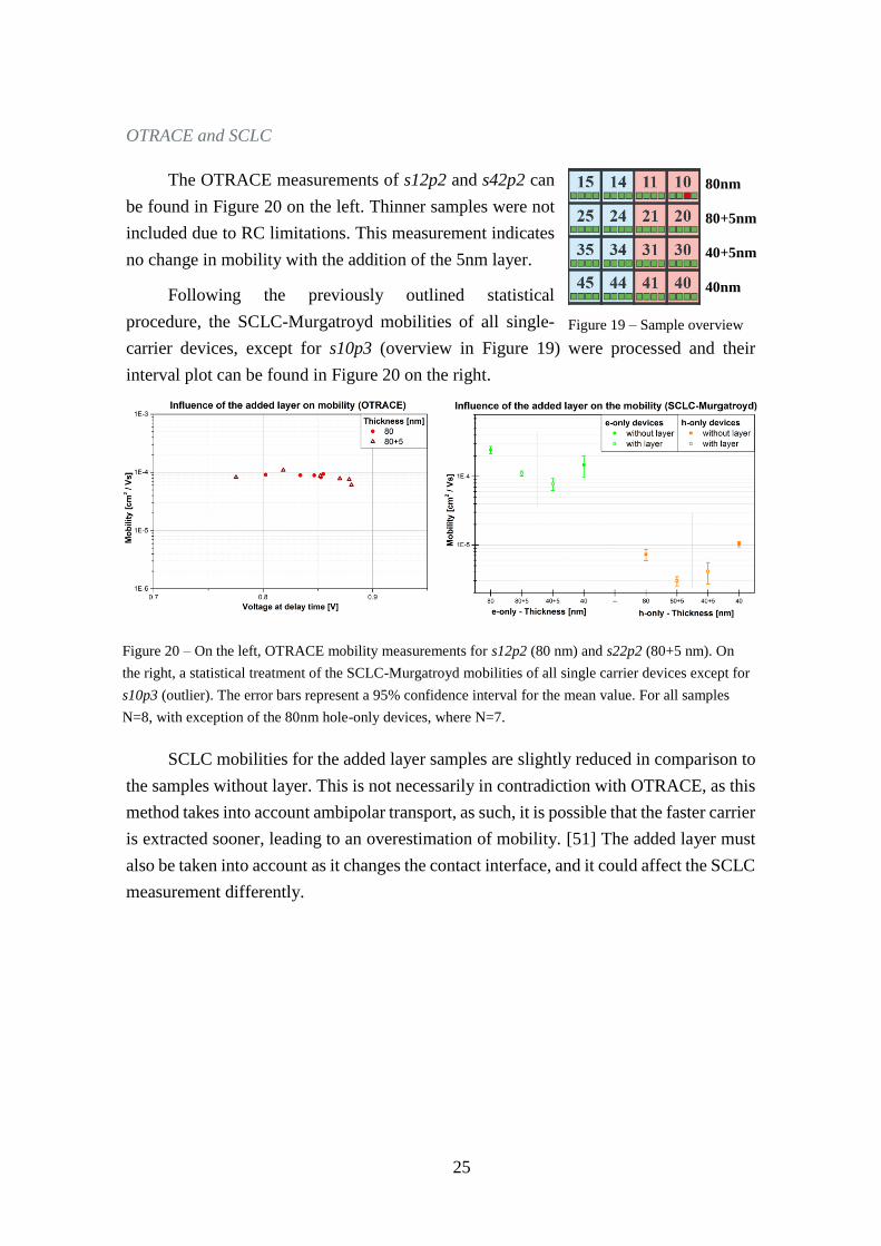
OTRACE and SCLC
The OTRACE measurements of s12p2 and s42p2 can
be found in Figure 20 on the left. Thinner samples were not
included due to RC limitations. This measurement indicates
no change in mobility with the addition of the 5nm layer.
Following the previously outlined statistical
procedure, the SCLC-Murgatroyd mobilities of all single-
carrier devices, except for s10p3 (overview in Figure 19) were processed and their
interval plot can be found in Figure 20 on the right.
SCLC mobilities for the added layer samples are slightly reduced in comparison to
the samples without layer. This is not necessarily in contradiction with OTRACE, as this
method takes into account ambipolar transport, as such, it is possible that the faster carrier
is extracted sooner, leading to an overestimation of mobility. [51] The added layer must
also be taken into account as it changes the contact interface, and it could affect the SCLC
measurement differently.
Figure 20 – On the left, OTRACE mobility measurements for s12p2 (80 nm) and s22p2 (80+5 nm). On
the right, a statistical treatment of the SCLC-Murgatroyd mobilities of all single carrier devices except for
s10p3 (outlier). The error bars represent a 95% confidence interval for the mean value. For all samples
N=8, with exception of the 80nm hole-only devices, where N=7.
80nm
80+5nm
40+5nm
40nm
Figure 19 – Sample overview

26
Suns-VOC - ni
In Figure 21, the intrinsic carrier density plot for s12p4 and s22p4 can be observed.
The plot suggests identical values for both samples. Table 5 presents a summary of the
mobilities, recombination constant and the intrinsic carrier density.
Table 5 – Summary of the mean value of the effective mobility from SCLC (Murgatroyd model), mobil-
ity and recombination constant from OTRACE (s12p2 and s22p2), as well as intrinsic carrier density
from Suns-VOC, for s12p4 (80 nm) and s22p4 (80+5 nm).
L [nm] Mean μeff – SCLC (Mt)
[cm2/Vs]
μ-OTRACE
[cm2/Vs] kr [cm3/μs]
ni
[cm-3]
80 4∙10-5 9∙10-5 3∙10-12 2∙109
80+5 2∙10-5 8∙10-5 4∙10-12 2∙109
Simulation
Parameters from Table 5 and Table 4 were taken into account, s12p4 and s22p4
were simulated as represented in Figure 22. Both simulations present reasonable fits, with
some overestimation of mobility in both cases, particularly in the 80+5 nm sample.
Figure 21 – Intrinsic carrier density plot of s12p4 (80 nm)
and s22p4 (80+5 nm). Dashed and solid lines represent sam-
ples with and without layer respectively.

27
Summary
In this run the addition of a 5nm protective layer caused no discernible change in
the JSC of all samples, as supported by EQE and JV measurements.
No change was also observed in the VOC according to the JV curves. Both the
ideality factor from Suns-VOC and the charge carrier lifetimes from TPV remained un-
changed after degradation, thus supporting a constant VOC.
JV measurements revealed that the addition of the layer can cause a reduction in
the average FF of up to approximately 8% for the 80 nm samples. Regarding the 40 nm
samples the same cannot be concluded due their large variabilities, although it should be
expected. While OTRACE measurements indicated no change in mobility, SCLC indi-
cated a slight reduction in the mobility of samples with the layer. This disagreement may
be due to an earlier extraction of faster carriers, thus leading to an overestimation in the
OTRACE mobility. A change in the contact interface due to the extra layer is also a pos-
sibility for a difference in the SCLC measurement. Simulations revealed reasonable fits
and overestimated mobilities for both unaged s12p4 (80 nm) and s22p4 (80+5 nm).
The addition of the protective layer caused a reduction in the average PCE of up
to approximately 1,3%. This was mostly due to a slight reduction in FF, itself due to a
slight reduction in mobility.
Figure 22 – Simulation of s12p4 (80 nm) and s22p4 (80+5 nm) on the left and right sides respectively.
Solid lines indicate a simulation based on the parameters, and dotted lines indicate experimental data.
28
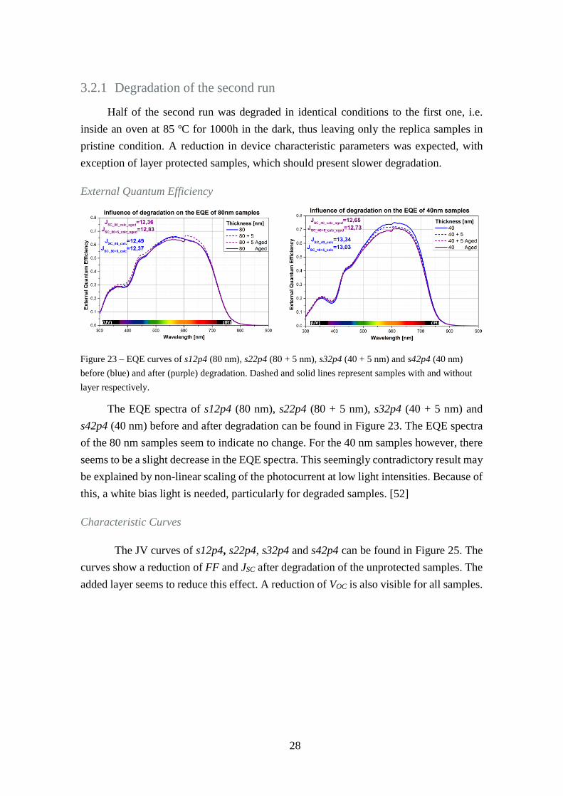
3.2.1 Degradation of the second run
Half of the second run was degraded in identical conditions to the first one, i.e.
inside an oven at 85 ºC for 1000h in the dark, thus leaving only the replica samples in
pristine condition. A reduction in device characteristic parameters was expected, with
exception of layer protected samples, which should present slower degradation.
External Quantum Efficiency
The EQE spectra of s12p4 (80 nm), s22p4 (80 + 5 nm), s32p4 (40 + 5 nm) and
s42p4 (40 nm) before and after degradation can be found in Figure 23. The EQE spectra
of the 80 nm samples seem to indicate no change. For the 40 nm samples however, there
seems to be a slight decrease in the EQE spectra. This seemingly contradictory result may
be explained by non-linear scaling of the photocurrent at low light intensities. Because of
this, a white bias light is needed, particularly for degraded samples. [52]
Characteristic Curves
The JV curves of s12p4, s22p4, s32p4 and s42p4 can be found in Figure 25. The
curves show a reduction of FF and JSC after degradation of the unprotected samples. The
added layer seems to reduce this effect. A reduction of VOC is also visible for all samples.
Figure 23 – EQE curves of s12p4 (80 nm), s22p4 (80 + 5 nm), s32p4 (40 + 5 nm) and s42p4 (40 nm)
before (blue) and after (purple) degradation. Dashed and solid lines represent samples with and without
layer respectively.

29
By following the previously outlined statistical procedures, interval plots
for the performance characteristics (JSC, VOC, FF and PCE) of all
degraded OSCs, with exception of s22p1 and s32p3, were made and can
be found in Figure 28. A more clear overview of these samples is
presented in Figure 24.
Firstly, larger variabilities can be seen for the 40 nm samples. The
average JSC of the 80+5* nm samples clearly suffered less degradation
when compared to the 80* nm samples. The same cannot be said of the
40+5* nm samples, whose large variabilities make comparisons more difficult, although
the average value is slightly higher and some preservation could have occurred. It is pos-
sible that the different optical interference patterns caused by different thicknesses, may
compromise the effectiveness of the protective layer. Regarding the FF, for 80+5* nm
samples a maximum of ≈12% in the average FF was conserved after degradation, when
compared with the 80 nm samples. VOC seems to have lowered slightly for all samples
(few tens of mV) with no effect from the layer. The unaged measurements were per-
formed in a warmer environment than the aged ones, as such, this reduction in VOC can
not be attributed to a difference in temperature, furthermore, this implies that the reduc-
tion in VOC is underestimated. The PCE reflects these effects, particularly the slower JSC
degradation. After 1000h of degradation, a maximum of ≈3,8% of the average PCE was
conserved by this layer when comparing the 80+5* nm to 80* nm degraded samples.
Figure 25 – Characteristic curves of s12p4 (80 nm), s22p4 (80 + 5 nm), s32p4 (40 + 5 nm) and s42p4 (40
nm) before (blue) and after (purple) degradation.
Figure 24 –
Sample over-
view
80nm
80+5nm
40+5nm
40nm

30
Suns-VOC
The ideality factor characterization of s12p4, s22p4, s32p4 and s42p4 can be found
in Figure 27. Recalling Eq. (1.11), and as observed in this characterization, there is no
Figure 26 – Interval plots of the performance characteristics of all degraded samples with exception of
s22p1 and s32p3. Vertical bars represent a 95% confidence interval for the mean value. Degraded sam-
ples are marked with *. The light blue lines connecting pristine to degraded samples are exclusively used
as a visual aid, their slopes can be compared to each other to estimate how differently degradation af-
fected each sample.
Figure 27 – Ideality factor characterization of s12p4 (80 nm), s22p4 (80+5 nm), s32p4 (40+5 nm) and
s42p4 (40 nm), before (blue) and after degradation (purple).

31
change in nid, thus there appears to be no change in the recombination mechanism after
degradation.
Transient Photovoltage
The charge carrier lifetime characterization for the same samples can be found in
Figure 28. The lifetime plots suggest an increase in charge carrier lifetime.
Taking into account the reduced VOC obtained by the JV curve, and that this reduc-
tion was not due to temperature, an increase in recombination is implied. Since nid has
not changed, the recombination mechanism is identical. Assuming that a broadening of
the density of states (DOS) has occurred, this would lead to a decrease in VOC, and in-
creased trapping of charge carriers, thus delaying recombination and increasing lifetime
as well as reducing mobility.
OTRACE and SCLC
The OTRACE mobility measurements for s12p2 and
s22p2 before and after degradation can be found in Figure 30 on
the left. Samples of lower thickness were not included due to RC
limitations. The OTRACE technique suggests no significant
change in mobility, which isn’t necessarily contradictory to a
small decrease in mobility, as OTRACE could have extracted
the faster carriers, thus leading to an overestimation of mobility.
Figure 28 – Charge carrier lifetime characterization of s12p4 (80 nm), s22p4 (80+5 nm), s32p4 (40+5
nm) and s42p4 (40 nm), before (blue) and after degradation (purple).
Figure 29 – Sample
overview

32
The previously outlined statistical procedure was followed, with exception for out-
lier exclusions. Interval plots for the SCLC-Murgatroyd mobility can be found in Figure
30 on the right. An overview of the samples used in the statistical treatment is located in
Figure 29. Unsuccessful fits are represented with no color; Only half of the run was de-
graded, thus the available number of samples for this analysis is halved, and unsuccessful
fits or outlier values can further reduce this number, therefore variabilities of these pa-
rameters are expected to increase in comparison to their unaged counterparts.
The SCLC mobility measurements suggest a reduction in electron mobility for all
samples, particulary for the 80 and 80+5 nm, and a decrease of approximately two orders
of magnitude in the hole mobility of all samples. Such a large decrease is indicative of
problems with the injection of charges due to degradation, particularly for hole-only de-
vices, additionally the number of failed fits is higher for these devices, further supporting
that SCLC is prone to contact problems and that fittings are troublesome for very low
mobility values.
Figure 30 – On the left, OTRACE mobility measurements for s12p2 (80 nm) and s22p2 (80+5 nm) before
and after degradation. On the right, SCLC for the electron and hole mobilites.
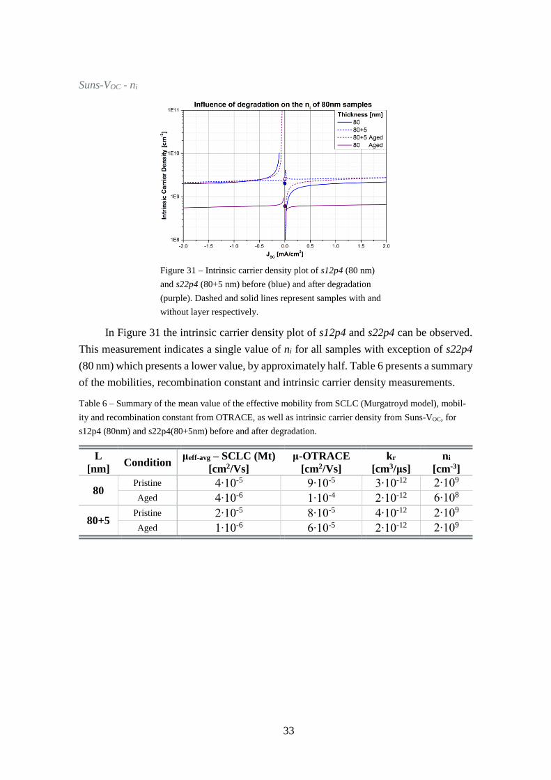
33
Suns-VOC - ni
In Figure 31 the intrinsic carrier density plot of s12p4 and s22p4 can be observed.
This measurement indicates a single value of ni for all samples with exception of s22p4
(80 nm) which presents a lower value, by approximately half. Table 6 presents a summary
of the mobilities, recombination constant and intrinsic carrier density measurements.
Table 6 – Summary of the mean value of the effective mobility from SCLC (Murgatroyd model), mobil-
ity and recombination constant from OTRACE, as well as intrinsic carrier density from Suns-VOC, for
s12p4 (80nm) and s22p4(80+5nm) before and after degradation.
L
[nm] Condition
μeff-avg – SCLC (Mt)
[cm2/Vs]
μ-OTRACE
[cm2/Vs]
kr
[cm3/μs]
ni
[cm-3]
80 Pristine 4∙10-5 9∙10-5 3∙10-12 2∙109
Aged 4∙10-6 1∙10-4 2∙10-12 6∙108
80+5 Pristine 2∙10-5 8∙10-5 4∙10-12 2∙109
Aged 1∙10-6 6∙10-5 2∙10-12 2∙109
Figure 31 – Intrinsic carrier density plot of s12p4 (80 nm)
and s22p4 (80+5 nm) before (blue) and after degradation
(purple). Dashed and solid lines represent samples with and
without layer respectively.

34
Simulation
The model parameters can be observed next to the simulations, in Figure 32. By
looking at the internal voltage curves, free of parasitic effects, a clear underestimation of
ni can be observed for s12p4, which due to the model of the ni measurement, suggests an
overestimation of mobility has occurred. More specifically, if the ni value of s12p4
(6∙108cm-3) were to be doubled, its mobility (1∙10-4cm2/Vs) would be halved, thus values
of 1,2∙109cm-3and 5∙10-5cm2/Vs would be obtained respectively. As such, a small reduc-
tion in mobility is possible but remains to be verified.
Summary
In this run, with high temperature degradation for 1000h in darkness, the 5nm
added layer was able to considerably slow down the degradation of the average JSC for
the 80+5nm samples (reduced by up to 3mA) when compared to the unprotected ones
(reduced by up to 8mA). The thinnest samples had large variabilities and although they
may suggest some protection of the layered samples, a statistical study with higher sam-
pling would be required for a more solid conclusion. The disagreement between JV curves
and EQE spectra can be attributed to the requirement of using a white bias light for the
latter, in the case of degraded OSCs.
A reduction in the VOC of all samples was observed, according to the JV curves.
The ideality factor from Suns-VOC remained unchanged, implying also no change in the
recombination mechanism. However, charge carrier lifetimes from TPV indicated an in-
crease upon ageing. This could be explained by a broadening of the density of states,
however a decrease in mobility is to be expected. To further investigate this hypothesis
Figure 32 – Simulation of unaged s12p4 (80 nm) and s22p4 (80+5 nm) on the left and right sides respectively. Solid
lines indicate the simulation based on shown parameters, and dotted lines indicate experimental data.

35
impedance spectroscopy measurements [56] or thermally stimulated current measure-
ments (TSC) [54,55] would be used.
JV curves determined a reduction in FF for all samples, however, for the 80+5
nm samples the layer was able to conserve up to ≈12% of the average FF in comparison
with the 80 nm samples. OTRACE indicated no change in mobility. In stark contrast,
SCLC indicated a reduction of approximately two orders of magnitude in hole mobility
and a smaller reduction in electron mobility. This could have been due bad contacts
caused by degradation, particularly for hole-only devices. Simulations revealed an agree-
able fit for s22p4 (80+5 nm) but not for s21p4 (80nm) which indicated an underestimation
of ni by a factor of 0,5 and thus implied an overestimation of mobility by a factor of 2.
Comparing the 80nm with the 80+5nm samples, a protection of up to ≈3,8% in
the average PCE was obtained. The added layer may cause an initial reduction in the
PCE, however, it is able to slow down degradation, thus making it a useful addition where
high longevity is required in an OSC.

36
4 Conclusions and Future Perspectives
In this thesis the effect of degradation on the charge transport and recombination
dynamics of photo-generated charges in organic photovoltaic devices was investigated.
An understanding of the relationship between characteristic device parameters and mate-
rial properties was developed.
The degradation (85ºC in darkness for 1000h) of OSCs, made with proprietary
materials from Heliatek GmbH was studied through the use of basic techniques (EQE,
JV) were used to obtain characteristic device parameters (JSC, VOC, FF, PCE), as well as
Suns-VOC (nid and ni) and TPV (τ – charge carrier lifetime) regarding recombination.
OTRACE (μ), a novel technique to measure mobility, was used, as well as SCLC (μe
and μh) with the Murgatroyd and Mott-Gurney models, of which the former was mostly
used. Simulations were performed based on the model by Neher [36]. Given such a high
temperature for degradation (85ºC), it is possible that the device reached or even sur-
passed the glass transition temperature of the HTL material, which would result in a loss
of its conductivity and in diffusion of dopants to the subsequent layer. [57]
Results of the first run indicate a reduction in PCE, mostly due to a reduction in
FF, itself due to extrinsic factors such as parasitic resistances. No difference in degrada-
tion was noted between the good batch and bad batch materials. In an attempt to slow
down degradation a 5nm protective layer was used in the second run. Results indicated
that the layer caused a reduction of up to 1,3% of average PCE, which was due mostly
to a reduction in FF, itself due to a slight reduction in mobility. Upon degradation of the
second run, results indicated a decrease in all parameters for all samples, although with
slower reduction of FF and a much more pronounced, slower reduction of JSC for the
80+5 nm samples. Thus the added layer was able to preserve up to ≈3,8% of average
PCE for these samples.
37
4.1 Future Perspectives
Additional measurements can be performed to obtain more information about the
samples studied in this thesis. Since there was a reduction in VOC for degradation of the
last run, it would be interesting to perform a sensitive EQE measurement [53], which re-
veals information on the CT state energy and recombination losses. Measurement of
EQE with a white bias light can reveal a reduction in the EQE spectrum for samples
with more advanced degradation [52].
For further understanding of recombination mechanisms, methods such as transi-
ent absorption spectroscopy (TAS) could be used, since this is an optical method it will
not subjected to electrical effects such as RC limitations or extraction losses. [39]
Regarding the previously stated hypothesis, that a broadening of the DOS would
be responsible for an increase in charge carrier lifetime, techniques such as thermally
stimulated current (TSC) [54,55] for trap state measurements, or impedance spectros-
copy [56] for carrier lifetime and DOS measurements, could be used to determine its va-
lidity.
Currently, there is no standard mobility measurement, thus a comparison of a se-
lect group, among the several available methods such as, POEM [19], TOF, OTRACE
[42,43], SCLC and other variants, would be relevant in determining their effectiveness
and validity over a range of materials, or parameters, such as conductivity.
A protective layer capable of slowing degradation would be greatly beneficial in
improving OSC longevity. As such, investigating possible connections between the pro-
tective effect of the layer and other variables, such as thickness, would be relevant.
Measurements of the surface roughness of this layer would also be relevant in under-
standing how to optimize the protection effect of the layer, while minimizing its initial
negative impact on OSC performance.

38
References
[1] R.E.P.N. for the 21st Century (REN21), Renewables 2016 - Global Status Report,
2016.
[2] E. Comission, “A policy framework for climate and energy in the period from 2020
to 2030,” Jan. 2014.
[3] F.M. for Economic Affairs and Energy, “Renewable Energy Sources Act,” Aug.
2014.
[4] N.S. Lewis and D.G. Nocera, “Powering the planet: Chemical challenges in solar
energy utilization,” Proceedings of the National Academy of Sciences, vol. 103,
2006, pp. 15729–15735.
[5] N.R.E.L. (NREL), “Best Research-Cell Efficiencies,” 2016.
[6] C.J. Brabec, “Organic photovoltaics: technology and market,” Solar energy
materials and solar cells, vol. 83, 2004, pp. 273–292.
[7] C.W. Tang, “Two-layer organic photovoltaic cell,” Applied Physics Letters, vol.
48, 1986.
[8] H. GmbH, Heliatek sets new Organic Photovoltaic world record efficiency of
13.2%, 2016.
[9] Heliatek, “Pilot Projects,” 2016.
[10] W. Tress, Organic Solar Cells - Theory, Experiment, and Device Simulation,
Springer, 2014.
[11] J. Zhao, Y. Li, G. Yang, K. Jiang, H. Lin, H. Ade, W. Ma, and H. Yan, “Efficient
organic solar cells processed from hydrocarbon solvents,” Nature Energy, vol. 1,
2016, p. 15027.
[12] K. Cnops, B.P. Rand, D. Cheyns, B. Verreet, M.A. Empl, and P. Heremans, “8.4%
efficient fullerene-free organic solar cells exploiting long-range exciton energy
transfer,” Nature communications, vol. 5, 2014.

39
[13] S. Albrecht, J.R. Tumbleston, S. Janietz, I. Dumsch, S. Allard, U. Scherf, H. Ade,
and D. Neher, “Quantifying Charge Extraction in Organic Solar Cells: The Case of
Fluorinated PCPDTBT,” The Journal of Physical Chemistry Letters, vol. 5, 2014,
pp. 1131–1138.
[14] B. Ray and M.A. Alam, “Achieving Fill Factor Above 80% in Organic Solar Cells
by Charged Interface,” Journal of Photovoltaics, 2012.
[15] M. Schwoerer and H.C. Wolf, Organic molecular solids, John Wiley & Sons, 2007.
[16] S.M. Sze, Physics of Semiconductor Devices, John Wiley & Sons, 1969.
[17] J. Cottaar, R. Coehoorn, and P. Bobbert, “Modeling of charge transport across
disordered organic heterojunctions,” Or, vol. 13, 2012, pp. 667–672.
[18] V. Kažukauskas, A. Arlauskas, M. Pranaitis, R. Lessmann, M. Riede, and K. Leo,
“Characterization of effective charge carrier mobility in ZnPc/C60 solar cells after
ageing,” physica status solidi (c), vol. 6, 2009, pp. 2864–2866.
[19] J. Widmer, J. Fischer, W. Tress, K. Leo, and M. Riede, “Electric potential mapping
by thickness variation: A new method for model-free mobility determination in
organic semiconductor thin films,” Organic Electronics, vol. 14, 2013, pp. 3460–
3471.
[20] N.F. Mott and R.W. Gurney, “Electronic processes in ionic crystals,” 1940.
[21] P.N. Murgatroyd, “Theory of space-charge-limited current enhanced by Frenkel
effect,” Applied Physics, vol. 3, 1970, pp. 151–156.
[22] W. Pasveer, J. Cottaar, C. Tanase, R. Coehoorn, P. Bobbert, P. Blom, D. De Leeuw,
and M. Michels, “Unified description of charge-carrier mobilities in disordered
semiconducting polymers,” Physical review letters, vol. 94, 2005, p. 206601.
[23] K. Vandewal, “Interfacial Charge Transfer States in Condensed Phase Systems,”
Annual review of physical chemistry, vol. 67, 2016, pp. 113–133.
[24] R.R. Lunt, N.C. Giebink, A.A. Belak, J.B. Benziger, and S.R. Forrest, “Exciton
diffusion lengths of organic semiconductor thin films measured by spectrally
resolved photoluminescence quenching,” Journal of Applied Physics, vol. 105,
2009.
[25] T.M. Clarke and J.R. Durrant, “Charge Photogeneration in Organic Solar Cells,”
Chemical Reviews, vol. 110, 2010, pp. 6736–6767.
[26] D. Wynands, B. Maennig, M. Riede, K. Leo, E. Brier, E. Reinold, and P. Baeuerle,
“Organic thin film photovoltaic cells based on planar and mixed heterojunctions
between fullerene and a low bandgap oligothiophene,” Journ, vol. 106, 2009.
[27] A. De Vos, “Detailed balance limit of the efficiency of tandem solar cells,” Journal
of Physics D: Applied Physics, vol. 13, 1979, pp. 839–846.
[28] C.W. Schlenker, V.S. Barlier, S.W. Chin, M.T. Whited, R.E. McAnally, S.R.
Forrest, and M.E. Thompson, “Cascade Organic Solar Cells,” Chemistry of
Materials, vol. 23, 2011, pp. 4132–4140.
[29] P. Wuerfel, “Physics of Solar Cells,” 2005.

40
[30] H. Hoppe, N. Arnold, D. Meissner, and N.S. Sariciftci, “Modeling of optical
absorption in conjugated polymer/fullerene bulk-heterojunction plastic solar cells,”
Thin Solid Films, vol. 451, 2004, pp. 589–592.
[31] B. Maennig, J. Drechsel, D. Gebeyehu, P. Simon, F. Kozlowski, A. Werner, F. Li,
S. Grundmann, S. Sonntag, M. Koch, K. Leo, M. Pfeiffer, H. Hoppe, D. Meissner,
N.S. Sariciftci, I. Riedel, V. Dyakonov, and J. Parisi, “Organic p-i-n solar cells,”
Applied Physics A, vol. 79, 2004, pp. 1–14.
[32] D. Nanova, M. Scherer, F. Schell, J. Zimmermann, T. Glaser, A.K. Kast, C.
Krekeler, A. Pucci, W. Kowalsky, R.R. Schröder, and others, “Why Inverted Small
Molecule Solar Cells Outperform Their Noninverted Counterparts,” Advanced
Functional Materials, vol. 25, 2015, pp. 6511–6518.
[33] U. Wuerfel, D. Neher, A. Spies, and S. Albrecht, “Impact of charge transport on
current-voltage characteristics and power-conversion efficiency of organic solar
cells,” Nature communications, 2015.
[34] W. Tress, S. Corvers, K. Leo, and M. Riede, “Investigation of Driving Forces for
Charge Extraction in Organic Solar Cells - Transient Photocurrent Measurements
on Solar Cells Showing S-Shaped Current–Voltage Characteristics,” Advanced
Energy Materials, 2013.
[35] W. Tress, K. Leo, and M. Riede, “Influence of Hole-Transport Layers and Donor
Materials on Open-Circuit Voltage and Shape of I–V Curves of Organic Solar
Cells,” Advanced Functional Materials, vol. 21, 2011, pp. 2140–2149.
[36] D. Neher, J. Kniepert, A. Elimelech, and L.J.A. Koster, “A New Figure of Merit for
Organic Solar Cells with Transport-limited Photocurrents,” Scientific reports, vol.
6, 2016.
[37] V. Shrotriya, G. Li, Y. Yao, T. Moriarty, K. Emery, and Y. Yang, “Accurate
measurement and characterization of organic solar cells,” Advanced Functional
Materials, vol. 16, 2006, pp. 2016–2023.
[38] N.R.E.L. (NREL), “Device Performance - Measurements & Characterization,” Jul.
2006.
[39] T.M. Clarke, C. Lungenschmied, J. Peet, N. Drolet, and A.J. Mozer, “A
Comparison of Five Experimental Techniques to Measure Charge Carrier Lifetime
in Polymer/Fullerene Solar Cells,” Advanced Energy Materials, vol. 5, 2015.
[40] E. Nakane, K. Kaneko, T. Mori, T. Mizutani, H. Takino, and M. Ishioka, “Effects
of electrodes on space charge in polypropylene,” CEIDP’05. 2005 Annual Report
Conference on Electrical Insulation and Dielectric Phenomena, 2005., IEEE, 2005,
pp. 653–656.
[41] A.J. Mozer, D. Dennler, N.S. Sariciftci, M. Westerling, and A. Pivrikas, “Time-
dependent mobility and recombination of the photoinducted charge carriers in
conjugated polymer/fullerene bulk heterojunction solar cells,” Faculty of Science,
Medicine and Health - Papers, vol. 72, 2005.
[42] A. Baumann, J. Lorrman, C. Deibel, and V. Dyakonov, “A New Approach for
Probing the Mobility and Lifetime of Photogenerated Charge Carriers in Organic
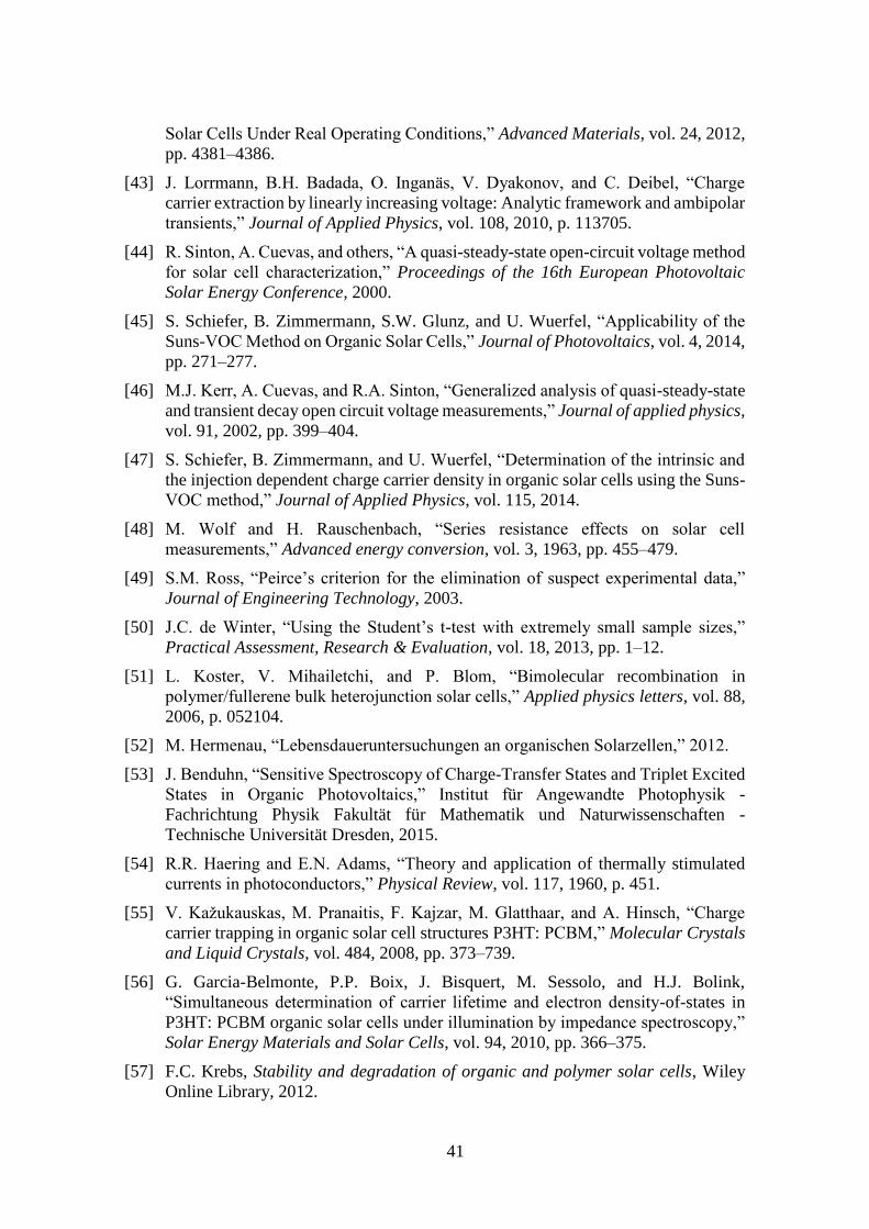
41
Solar Cells Under Real Operating Conditions,” Advanced Materials, vol. 24, 2012,
pp. 4381–4386.
[43] J. Lorrmann, B.H. Badada, O. Inganäs, V. Dyakonov, and C. Deibel, “Charge
carrier extraction by linearly increasing voltage: Analytic framework and ambipolar
transients,” Journal of Applied Physics, vol. 108, 2010, p. 113705.
[44] R. Sinton, A. Cuevas, and others, “A quasi-steady-state open-circuit voltage method
for solar cell characterization,” Proceedings of the 16th European Photovoltaic
Solar Energy Conference, 2000.
[45] S. Schiefer, B. Zimmermann, S.W. Glunz, and U. Wuerfel, “Applicability of the
Suns-VOC Method on Organic Solar Cells,” Journal of Photovoltaics, vol. 4, 2014,
pp. 271–277.
[46] M.J. Kerr, A. Cuevas, and R.A. Sinton, “Generalized analysis of quasi-steady-state
and transient decay open circuit voltage measurements,” Journal of applied physics,
vol. 91, 2002, pp. 399–404.
[47] S. Schiefer, B. Zimmermann, and U. Wuerfel, “Determination of the intrinsic and
the injection dependent charge carrier density in organic solar cells using the Suns-
VOC method,” Journal of Applied Physics, vol. 115, 2014.
[48] M. Wolf and H. Rauschenbach, “Series resistance effects on solar cell
measurements,” Advanced energy conversion, vol. 3, 1963, pp. 455–479.
[49] S.M. Ross, “Peirce’s criterion for the elimination of suspect experimental data,”
Journal of Engineering Technology, 2003.
[50] J.C. de Winter, “Using the Student’s t-test with extremely small sample sizes,”
Practical Assessment, Research & Evaluation, vol. 18, 2013, pp. 1–12.
[51] L. Koster, V. Mihailetchi, and P. Blom, “Bimolecular recombination in
polymer/fullerene bulk heterojunction solar cells,” Applied physics letters, vol. 88,
2006, p. 052104.
[52] M. Hermenau, “Lebensdaueruntersuchungen an organischen Solarzellen,” 2012.
[53] J. Benduhn, “Sensitive Spectroscopy of Charge-Transfer States and Triplet Excited
States in Organic Photovoltaics,” Institut für Angewandte Photophysik -
Fachrichtung Physik Fakultät für Mathematik und Naturwissenschaften -
Technische Universität Dresden, 2015.
[54] R.R. Haering and E.N. Adams, “Theory and application of thermally stimulated
currents in photoconductors,” Physical Review, vol. 117, 1960, p. 451.
[55] V. Kažukauskas, M. Pranaitis, F. Kajzar, M. Glatthaar, and A. Hinsch, “Charge
carrier trapping in organic solar cell structures P3HT: PCBM,” Molecular Crystals
and Liquid Crystals, vol. 484, 2008, pp. 373–739.
[56] G. Garcia-Belmonte, P.P. Boix, J. Bisquert, M. Sessolo, and H.J. Bolink,
“Simultaneous determination of carrier lifetime and electron density-of-states in
P3HT: PCBM organic solar cells under illumination by impedance spectroscopy,”
Solar Energy Materials and Solar Cells, vol. 94, 2010, pp. 366–375.
[57] F.C. Krebs, Stability and degradation of organic and polymer solar cells, Wiley
Online Library, 2012.


43
Annex


45
Annex A – Physical Constants
Description Value
Speed of light in vacuum – c 2.99792∙108 [m/s]
Elementary charge – q 1.60218∙10-19 [As]
Planck’s constant – h 6.60627∙10-34 [Js]
Boltzmann’s constant – kB 1.38065∙1023 [J/K]
Vaccuum permitivity – ϵ0 8.85419∙10-12 [A2s4 (kg m3)-1]
Annex B – Acronyms
PV Photovoltaic
OPV Organic Photovoltaic
BIPV Building Integrated Photovoltaic
PCE Power Conversion Efficiency
FF
OSC
HOMO
LUMO
DA
CT
FHJ
BHJ
PMHJ
HTL
ETL
ITO
EQE
Fill Factor
Organic Solar Cell
Highest Occupied Molecular Orbit
Lowest Unoccupied Molecular Orbit
Donor-Acceptor
Charge-Transfer
Flat Heterojunction
Bulk Heterojunction
Planar-Mixed Heterojunction
Hole Transport Layer
Electron Transport Layer
Indium-Tin-Oxide
External Quantum Efficiency
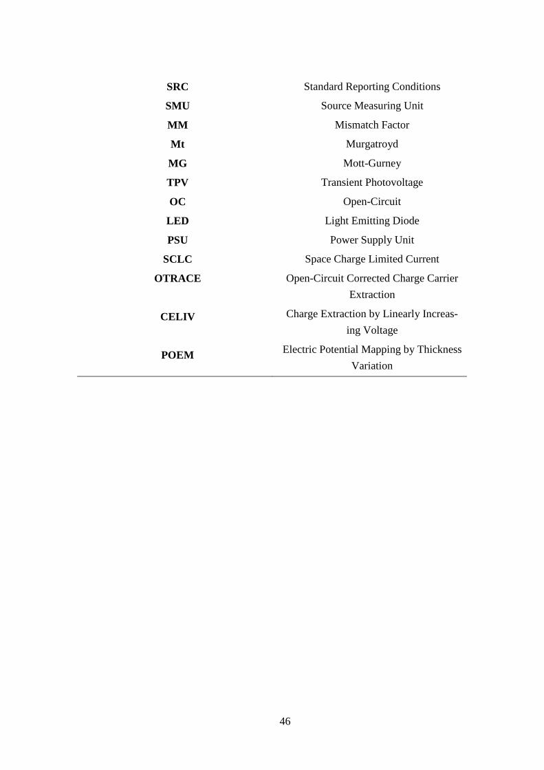
46
SRC
SMU
MM
Mt
MG
TPV
OC
LED
PSU
SCLC
OTRACE
CELIV
POEM
Standard Reporting Conditions
Source Measuring Unit
Mismatch Factor
Murgatroyd
Mott-Gurney
Transient Photovoltage
Open-Circuit
Light Emitting Diode
Power Supply Unit
Space Charge Limited Current
Open-Circuit Corrected Charge Carrier
Extraction
Charge Extraction by Linearly Increas-
ing Voltage
Electric Potential Mapping by Thickness
Variation

47
Annex C – Pixel Areas
1 2 3 4
p4: 2.540 x 2.540 [mm] + 0.09 mm2 =
6.440 mm2
p3: 1.270 x 2.540 [mm] + 0.09 mm2 =
3.316 mm2
p2: 0.898 x 2.540 [mm] + 0.09 mm2 =
2.371 mm2
p1: 1.796 x 2.540 [mm] + 0.09 mm2 =
4.652 mm2

48
Annex D – Heliatek 1st run planning sheet

49
Annex E - Heliatek 2nd run planning sheet

50
Annex F – SCLC models
In this case the single carrier device presents ohmic contacts (data points parallel to
dark green line for low voltages) and for higher voltages the device reaches SCLC (data
points parallel to light green line) with very little field dependence (γ = 2∙10-4 /cm V ),
thus both models (solid lines) are adequate for fitting and present similar values, 6∙10-5
cm2/Vs for the Mott-Gurney model and 4∙10-5 cm2/Vs for the Murgatroyd model.
This device also has ohmic contacts, however its mobility field-dependence is
higher (γ = 1∙10-3 /cm V ), thus the Murgatroyd model is more realistic in its mobility
value (1∙10-10 cm2/Vs) in comparison with the Mott-Gurney model (8∙10-8 cm2/Vs)
51
Annex G – TPV fit
The left side shows a single TPV measurement, which is then fitted according to
the exponential decay equation and its lifetime is obtained (11.5 μs). The value for VOC
(811.7 mV) is taken from the decay tail as it stabilizes, which ideally should match the
plateau located just before the excitation pulse, otherwise errors due to fitting may occur.
This procedure is repeated from low to high light intensities and the plot on the right is
obtained.
Annex H – ni fit
The determination of RS and the voltage difference (dV) between the pseudo (red)
and 1 sun (black) JV curves is located on the left. For this plot the slope directly shows
RS in kΩ (3.5Ω). At the conditions of this fit (high current in forward direction) Rtr(J)≈ 0,
thus ( ) ( )S circ trR J R R J becomes ( )S circR J R , where Rcirc is related to the circuitry
of the device. Therefore by knowing Rcirc, Rtr(J) can be calculated. [47]
The voltage differential dV was obtained by interpolation of both plots in the yellow
region, as noted on the left, and subtracting them. By applying these parameters to Eq.
(1.12), the ni(J) plot can be obtained as shown on the right. The ni value at 1sun (thus J=

52
0) can be determined through extrapolation from the rest of the curve. A pole at this in-
tensity can be observed due to the fact that there is no current flowing. [47]
Annex I – OTRACE
An OTRACE extraction curve at a single delay time is represented above. The max-
imum and lower level points are determined, respectively in blue and green, as well as
the indicated parameters, tmax, Δj and j0. This is repeated for the remaining delay times,
where each point in an OTRACE plot corresponds to a delay time. These parameters can
then be used with Eq. (1.10) to determine the mobility, as well as other parameters.
[42,43]


![Influence of pH on Soil Charge Characteristics and Cadmium … · 2019. 8. 1. · variable charge, the major factors are pH and ionic strength (I)[3]. The variable charge in soils](https://static.fdocuments.in/doc/165x107/611354b0252b9811f61bec3f/influence-of-ph-on-soil-charge-characteristics-and-cadmium-2019-8-1-variable.jpg)