iNEMO inertial module: always-on 3D accelerometer and 3D...
113
This is information on a product in full production. October 2016 DocID028475 Rev 5 1/113 LSM6DSL iNEMO inertial module: always-on 3D accelerometer and 3D gyroscope Datasheet - production data Features Power consumption: 0.4 mA in combo normal mode and 0.65 mA in combo high-performance mode “Always-on” experience with low power consumption for both accelerometer and gyroscope Smart FIFO up to 4 kbyte based on features set Android M compliant Hard, soft ironing for external magnetic sensor corrections ±2/±4/±8/±16 g full scale ±125/±245/±500/±1000/±2000 dps full scale Analog supply voltage: 1.71 V to 3.6 V Independent IOs supply (1.62 V) Compact footprint, 2.5 mm x 3 mm x 0.83 mm SPI & I 2 C serial interface with main processor data synchronization feature Pedometer, step detector and step counter Significant motion and tilt function Standard interrupts: free-fall, wakeup, 6D/4D orientation, click and double-click Embedded temperature sensor ECOPACK ® , RoHS and “Green” compliant Applications Motion tracking and gesture detection Collecting sensor data Indoor navigation IoT and connected devices Intelligent power saving for handheld devices Vibration monitoring and compensation Description The LSM6DSL is a system-in-package featuring a 3D digital accelerometer and a 3D digital gyroscope performing at 0.65 mA in high-performance mode and enabling always-on low-power features for an optimal motion experience for the consumer. The LSM6DSL supports main OS requirements, offering real, virtual and batch sensors with 4 kbyte for dynamic data batching. ST’s family of MEMS sensor modules leverages the robust and mature manufacturing processes already used for the production of micromachined accelerometers and gyroscopes. The various sensing elements are manufactured using specialized micromachining processes, while the IC interfaces are developed using CMOS technology that allows the design of a dedicated circuit which is trimmed to better match the characteristics of the sensing element. The LSM6DSL has a full-scale acceleration range of ±2/±4/±8/±16 g and an angular rate range of ±125/±245/±500/±1000/±2000 dps. High robustness to mechanical shock makes the LSM6DSL the preferred choice of system designers for the creation and manufacturing of reliable products. The LSM6DSL is available in a plastic land grid array (LGA) package. LGA-14L (2.5 x 3 x 0.83 mm) typ. Table 1. Device summary Part number Temp. range [°C] Package Packing LSM6DSL -40 to +85 LGA-14L (2.5x3x0.83mm) Tray LSM6DSLTR -40 to +85 Tape & Reel www.st.com
Transcript of iNEMO inertial module: always-on 3D accelerometer and 3D...

This is information on a product in full production.
October 2016 DocID028475 Rev 5 1/113
LSM6DSL
iNEMO inertial module: always-on 3D accelerometer and 3D gyroscope
Datasheet - production data
Features Power consumption: 0.4 mA in combo normal mode
and 0.65 mA in combo high-performance mode “Always-on” experience with low power
consumption for both accelerometer and gyroscope Smart FIFO up to 4 kbyte based on features set Android M compliant Hard, soft ironing for external magnetic sensor
corrections ±2/±4/±8/±16 g full scale ±125/±245/±500/±1000/±2000 dps full scale Analog supply voltage: 1.71 V to 3.6 V Independent IOs supply (1.62 V) Compact footprint, 2.5 mm x 3 mm x 0.83 mm SPI & I2C serial interface with main processor data
synchronization feature Pedometer, step detector and step counter Significant motion and tilt function Standard interrupts: free-fall, wakeup, 6D/4D
orientation, click and double-click Embedded temperature sensor ECOPACK®, RoHS and “Green” compliant
Applications Motion tracking and gesture detection Collecting sensor data Indoor navigation IoT and connected devices Intelligent power saving for handheld devices Vibration monitoring and compensation
DescriptionThe LSM6DSL is a system-in-package featuring a 3D digital accelerometer and a 3D digital gyroscope performing at 0.65 mA in high-performance mode and enabling always-on low-power features for an optimal motion experience for the consumer.
The LSM6DSL supports main OS requirements, offering real, virtual and batch sensors with 4 kbyte for dynamic data batching.
ST’s family of MEMS sensor modules leverages the robust and mature manufacturing processes already used for the production of micromachined accelerometers and gyroscopes.
The various sensing elements are manufactured using specialized micromachining processes, while the IC interfaces are developed using CMOS technology that allows the design of a dedicated circuit which is trimmed to better match the characteristics of the sensing element.
The LSM6DSL has a full-scale acceleration range of ±2/±4/±8/±16 g and an angular rate range of ±125/±245/±500/±1000/±2000 dps.
High robustness to mechanical shock makes theLSM6DSL the preferred choice of system designers forthe creation and manufacturing of reliable products.
The LSM6DSL is available in a plastic land grid array (LGA) package.
LGA-14L (2.5 x 3 x 0.83 mm) typ.
Table 1. Device summary
Part number Temp. range [°C] Package Packing
LSM6DSL -40 to +85LGA-14L
(2.5x3x0.83mm)
Tray
LSM6DSLTR -40 to +85 Tape & Reel
www.st.com
Contents LSM6DSL
2/113 DocID028475 Rev 5
Contents
1 Overview . . . . . . . . . . . . . . . . . . . . . . . . . . . . . . . . . . . . . . . . . . . . . . . . . 15
2 Embedded low-power features . . . . . . . . . . . . . . . . . . . . . . . . . . . . . . . 162.1 Tilt detection . . . . . . . . . . . . . . . . . . . . . . . . . . . . . . . . . . . . . . . . . . . . . . . 16
2.2 Absolute wrist tilt . . . . . . . . . . . . . . . . . . . . . . . . . . . . . . . . . . . . . . . . . . . . 17
3 Pin description . . . . . . . . . . . . . . . . . . . . . . . . . . . . . . . . . . . . . . . . . . . . 183.1 Pin connections . . . . . . . . . . . . . . . . . . . . . . . . . . . . . . . . . . . . . . . . . . . . 19
4 Module specifications . . . . . . . . . . . . . . . . . . . . . . . . . . . . . . . . . . . . . . . 214.1 Mechanical characteristics . . . . . . . . . . . . . . . . . . . . . . . . . . . . . . . . . . . . 21
4.2 Electrical characteristics . . . . . . . . . . . . . . . . . . . . . . . . . . . . . . . . . . . . . . 24
4.3 Temperature sensor characteristics . . . . . . . . . . . . . . . . . . . . . . . . . . . . . 25
4.4 Communication interface characteristics . . . . . . . . . . . . . . . . . . . . . . . . . 264.4.1 SPI - serial peripheral interface . . . . . . . . . . . . . . . . . . . . . . . . . . . . . . . 26
4.4.2 I2C - inter-IC control interface . . . . . . . . . . . . . . . . . . . . . . . . . . . . . . . . 27
4.5 Absolute maximum ratings . . . . . . . . . . . . . . . . . . . . . . . . . . . . . . . . . . . . 28
4.6 Terminology . . . . . . . . . . . . . . . . . . . . . . . . . . . . . . . . . . . . . . . . . . . . . . . 294.6.1 Sensitivity . . . . . . . . . . . . . . . . . . . . . . . . . . . . . . . . . . . . . . . . . . . . . . . . 29
4.6.2 Zero-g and zero-rate level . . . . . . . . . . . . . . . . . . . . . . . . . . . . . . . . . . . 29
5 Functionality . . . . . . . . . . . . . . . . . . . . . . . . . . . . . . . . . . . . . . . . . . . . . . 305.1 Operating modes . . . . . . . . . . . . . . . . . . . . . . . . . . . . . . . . . . . . . . . . . . . 30
5.2 Gyroscope power modes . . . . . . . . . . . . . . . . . . . . . . . . . . . . . . . . . . . . . 30
5.3 Accelerometer power modes . . . . . . . . . . . . . . . . . . . . . . . . . . . . . . . . . . 30
5.4 Block diagram of filters . . . . . . . . . . . . . . . . . . . . . . . . . . . . . . . . . . . . . . . 315.4.1 Block diagrams of the gyroscope filters . . . . . . . . . . . . . . . . . . . . . . . . . 31
5.4.2 Block diagrams of the accelerometer filters . . . . . . . . . . . . . . . . . . . . . . 32
5.5 FIFO . . . . . . . . . . . . . . . . . . . . . . . . . . . . . . . . . . . . . . . . . . . . . . . . . . . . . 335.5.1 Bypass mode . . . . . . . . . . . . . . . . . . . . . . . . . . . . . . . . . . . . . . . . . . . . . 33
5.5.2 FIFO mode . . . . . . . . . . . . . . . . . . . . . . . . . . . . . . . . . . . . . . . . . . . . . . . 34
5.5.3 Continuous mode . . . . . . . . . . . . . . . . . . . . . . . . . . . . . . . . . . . . . . . . . . 34
5.5.4 Continuous-to-FIFO mode . . . . . . . . . . . . . . . . . . . . . . . . . . . . . . . . . . . 34
DocID028475 Rev 5 3/113
LSM6DSL Contents
113
5.5.5 Bypass-to-Continuous mode . . . . . . . . . . . . . . . . . . . . . . . . . . . . . . . . . 34
5.5.6 FIFO reading procedure . . . . . . . . . . . . . . . . . . . . . . . . . . . . . . . . . . . . 35
6 Digital interfaces . . . . . . . . . . . . . . . . . . . . . . . . . . . . . . . . . . . . . . . . . . . 366.1 I2C/SPI interface . . . . . . . . . . . . . . . . . . . . . . . . . . . . . . . . . . . . . . . . . . . . 36
6.2 Master I2C . . . . . . . . . . . . . . . . . . . . . . . . . . . . . . . . . . . . . . . . . . . . . . . . 36
6.3 I2C serial interface . . . . . . . . . . . . . . . . . . . . . . . . . . . . . . . . . . . . . . . . . . 376.3.1 I2C operation . . . . . . . . . . . . . . . . . . . . . . . . . . . . . . . . . . . . . . . . . . . . . 37
6.4 SPI bus interface . . . . . . . . . . . . . . . . . . . . . . . . . . . . . . . . . . . . . . . . . . . 396.4.1 SPI read . . . . . . . . . . . . . . . . . . . . . . . . . . . . . . . . . . . . . . . . . . . . . . . . . 40
6.4.2 SPI write . . . . . . . . . . . . . . . . . . . . . . . . . . . . . . . . . . . . . . . . . . . . . . . . 41
6.4.3 SPI read in 3-wire mode . . . . . . . . . . . . . . . . . . . . . . . . . . . . . . . . . . . . 42
7 Application hints . . . . . . . . . . . . . . . . . . . . . . . . . . . . . . . . . . . . . . . . . . . 437.1 LSM6DSL electrical connections in Mode 1 . . . . . . . . . . . . . . . . . . . . . . . 43
7.2 LSM6DSL electrical connections in Mode 2 . . . . . . . . . . . . . . . . . . . . . . . 44
8 Register mapping . . . . . . . . . . . . . . . . . . . . . . . . . . . . . . . . . . . . . . . . . . 47
9 Register description . . . . . . . . . . . . . . . . . . . . . . . . . . . . . . . . . . . . . . . . 519.1 FUNC_CFG_ACCESS (01h) . . . . . . . . . . . . . . . . . . . . . . . . . . . . . . . . . . 51
9.2 SENSOR_SYNC_TIME_FRAME (04h) . . . . . . . . . . . . . . . . . . . . . . . . . . 51
9.3 SENSOR_SYNC_RES_RATIO (05h) . . . . . . . . . . . . . . . . . . . . . . . . . . . . 52
9.4 FIFO_CTRL1 (06h) . . . . . . . . . . . . . . . . . . . . . . . . . . . . . . . . . . . . . . . . . 52
9.5 FIFO_CTRL2 (07h) . . . . . . . . . . . . . . . . . . . . . . . . . . . . . . . . . . . . . . . . . 53
9.6 FIFO_CTRL3 (08h) . . . . . . . . . . . . . . . . . . . . . . . . . . . . . . . . . . . . . . . . . 54
9.7 FIFO_CTRL4 (09h) . . . . . . . . . . . . . . . . . . . . . . . . . . . . . . . . . . . . . . . . . 55
9.8 FIFO_CTRL5 (0Ah) . . . . . . . . . . . . . . . . . . . . . . . . . . . . . . . . . . . . . . . . . 56
9.9 DRDY_PULSE_CFG_G (0Bh) . . . . . . . . . . . . . . . . . . . . . . . . . . . . . . . . . 57
9.10 INT1_CTRL (0Dh) . . . . . . . . . . . . . . . . . . . . . . . . . . . . . . . . . . . . . . . . . . 57
9.11 INT2_CTRL (0Eh) . . . . . . . . . . . . . . . . . . . . . . . . . . . . . . . . . . . . . . . . . . 58
9.12 WHO_AM_I (0Fh) . . . . . . . . . . . . . . . . . . . . . . . . . . . . . . . . . . . . . . . . . . . 58
9.13 CTRL1_XL (10h) . . . . . . . . . . . . . . . . . . . . . . . . . . . . . . . . . . . . . . . . . . . 59
9.14 CTRL2_G (11h) . . . . . . . . . . . . . . . . . . . . . . . . . . . . . . . . . . . . . . . . . . . . 60
9.15 CTRL3_C (12h) . . . . . . . . . . . . . . . . . . . . . . . . . . . . . . . . . . . . . . . . . . . . 61
Contents LSM6DSL
4/113 DocID028475 Rev 5
9.16 CTRL4_C (13h) . . . . . . . . . . . . . . . . . . . . . . . . . . . . . . . . . . . . . . . . . . . . 62
9.17 CTRL5_C (14h) . . . . . . . . . . . . . . . . . . . . . . . . . . . . . . . . . . . . . . . . . . . . 62
9.18 CTRL6_C (15h) . . . . . . . . . . . . . . . . . . . . . . . . . . . . . . . . . . . . . . . . . . . . 64
9.19 CTRL7_G (16h) . . . . . . . . . . . . . . . . . . . . . . . . . . . . . . . . . . . . . . . . . . . . 65
9.20 CTRL8_XL (17h) . . . . . . . . . . . . . . . . . . . . . . . . . . . . . . . . . . . . . . . . . . . 65
9.21 CTRL9_XL (18h) . . . . . . . . . . . . . . . . . . . . . . . . . . . . . . . . . . . . . . . . . . . 66
9.22 CTRL10_C (19h) . . . . . . . . . . . . . . . . . . . . . . . . . . . . . . . . . . . . . . . . . . . 67
9.23 MASTER_CONFIG (1Ah) . . . . . . . . . . . . . . . . . . . . . . . . . . . . . . . . . . . . . 67
9.24 WAKE_UP_SRC (1Bh) . . . . . . . . . . . . . . . . . . . . . . . . . . . . . . . . . . . . . . . 68
9.25 TAP_SRC (1Ch) . . . . . . . . . . . . . . . . . . . . . . . . . . . . . . . . . . . . . . . . . . . . 69
9.26 D6D_SRC (1Dh) . . . . . . . . . . . . . . . . . . . . . . . . . . . . . . . . . . . . . . . . . . . . 70
9.27 STATUS_REG (1Eh) . . . . . . . . . . . . . . . . . . . . . . . . . . . . . . . . . . . . . . . . 70
9.28 OUT_TEMP_L (20h), OUT_TEMP_H (21h) . . . . . . . . . . . . . . . . . . . . . . . 71
9.29 OUTX_L_G (22h) . . . . . . . . . . . . . . . . . . . . . . . . . . . . . . . . . . . . . . . . . . . 71
9.30 OUTX_H_G (23h) . . . . . . . . . . . . . . . . . . . . . . . . . . . . . . . . . . . . . . . . . . . 71
9.31 OUTY_L_G (24h) . . . . . . . . . . . . . . . . . . . . . . . . . . . . . . . . . . . . . . . . . . . 72
9.32 OUTY_H_G (25h) . . . . . . . . . . . . . . . . . . . . . . . . . . . . . . . . . . . . . . . . . . . 72
9.33 OUTZ_L_G (26h) . . . . . . . . . . . . . . . . . . . . . . . . . . . . . . . . . . . . . . . . . . . 72
9.34 OUTZ_H_G (27h) . . . . . . . . . . . . . . . . . . . . . . . . . . . . . . . . . . . . . . . . . . . 73
9.35 OUTX_L_XL (28h) . . . . . . . . . . . . . . . . . . . . . . . . . . . . . . . . . . . . . . . . . . 73
9.36 OUTX_H_XL (29h) . . . . . . . . . . . . . . . . . . . . . . . . . . . . . . . . . . . . . . . . . . 73
9.37 OUTY_L_XL (2Ah) . . . . . . . . . . . . . . . . . . . . . . . . . . . . . . . . . . . . . . . . . . 73
9.38 OUTY_H_XL (2Bh) . . . . . . . . . . . . . . . . . . . . . . . . . . . . . . . . . . . . . . . . . . 74
9.39 OUTZ_L_XL (2Ch) . . . . . . . . . . . . . . . . . . . . . . . . . . . . . . . . . . . . . . . . . . 74
9.40 OUTZ_H_XL (2Dh) . . . . . . . . . . . . . . . . . . . . . . . . . . . . . . . . . . . . . . . . . . 74
9.41 SENSORHUB1_REG (2Eh) . . . . . . . . . . . . . . . . . . . . . . . . . . . . . . . . . . . 74
9.42 SENSORHUB2_REG (2Fh) . . . . . . . . . . . . . . . . . . . . . . . . . . . . . . . . . . . 75
9.43 SENSORHUB3_REG (30h) . . . . . . . . . . . . . . . . . . . . . . . . . . . . . . . . . . . 75
9.44 SENSORHUB4_REG (31h) . . . . . . . . . . . . . . . . . . . . . . . . . . . . . . . . . . . 75
9.45 SENSORHUB5_REG (32h) . . . . . . . . . . . . . . . . . . . . . . . . . . . . . . . . . . . 75
9.46 SENSORHUB6_REG (33h) . . . . . . . . . . . . . . . . . . . . . . . . . . . . . . . . . . . 76
9.47 SENSORHUB7_REG (34h) . . . . . . . . . . . . . . . . . . . . . . . . . . . . . . . . . . . 76
9.48 SENSORHUB8_REG(35h) . . . . . . . . . . . . . . . . . . . . . . . . . . . . . . . . . . . 76

DocID028475 Rev 5 5/113
LSM6DSL Contents
113
9.49 SENSORHUB9_REG (36h) . . . . . . . . . . . . . . . . . . . . . . . . . . . . . . . . . . . 76
9.50 SENSORHUB10_REG (37h) . . . . . . . . . . . . . . . . . . . . . . . . . . . . . . . . . . 77
9.51 SENSORHUB11_REG (38h) . . . . . . . . . . . . . . . . . . . . . . . . . . . . . . . . . . 77
9.52 SENSORHUB12_REG (39h) . . . . . . . . . . . . . . . . . . . . . . . . . . . . . . . . . . 77
9.53 FIFO_STATUS1 (3Ah) . . . . . . . . . . . . . . . . . . . . . . . . . . . . . . . . . . . . . . . 77
9.54 FIFO_STATUS2 (3Bh) . . . . . . . . . . . . . . . . . . . . . . . . . . . . . . . . . . . . . . . 78
9.55 FIFO_STATUS3 (3Ch) . . . . . . . . . . . . . . . . . . . . . . . . . . . . . . . . . . . . . . . 78
9.56 FIFO_STATUS4 (3Dh) . . . . . . . . . . . . . . . . . . . . . . . . . . . . . . . . . . . . . . . 79
9.57 FIFO_DATA_OUT_L (3Eh) . . . . . . . . . . . . . . . . . . . . . . . . . . . . . . . . . . . . 79
9.58 FIFO_DATA_OUT_H (3Fh) . . . . . . . . . . . . . . . . . . . . . . . . . . . . . . . . . . . 79
9.59 TIMESTAMP0_REG (40h) . . . . . . . . . . . . . . . . . . . . . . . . . . . . . . . . . . . . 80
9.60 TIMESTAMP1_REG (41h) . . . . . . . . . . . . . . . . . . . . . . . . . . . . . . . . . . . . 80
9.61 TIMESTAMP2_REG (42h) . . . . . . . . . . . . . . . . . . . . . . . . . . . . . . . . . . . . 80
9.62 STEP_TIMESTAMP_L (49h) . . . . . . . . . . . . . . . . . . . . . . . . . . . . . . . . . . 81
9.63 STEP_TIMESTAMP_H (4Ah) . . . . . . . . . . . . . . . . . . . . . . . . . . . . . . . . . . 81
9.64 STEP_COUNTER_L (4Bh) . . . . . . . . . . . . . . . . . . . . . . . . . . . . . . . . . . . 81
9.65 STEP_COUNTER_H (4Ch) . . . . . . . . . . . . . . . . . . . . . . . . . . . . . . . . . . . 82
9.66 SENSORHUB13_REG (4Dh) . . . . . . . . . . . . . . . . . . . . . . . . . . . . . . . . . . 82
9.67 SENSORHUB14_REG (4Eh) . . . . . . . . . . . . . . . . . . . . . . . . . . . . . . . . . . 82
9.68 SENSORHUB15_REG (4Fh) . . . . . . . . . . . . . . . . . . . . . . . . . . . . . . . . . . 82
9.69 SENSORHUB16_REG (50h) . . . . . . . . . . . . . . . . . . . . . . . . . . . . . . . . . . 83
9.70 SENSORHUB17_REG (51h) . . . . . . . . . . . . . . . . . . . . . . . . . . . . . . . . . . 83
9.71 SENSORHUB18_REG (52h) . . . . . . . . . . . . . . . . . . . . . . . . . . . . . . . . . . 83
9.72 FUNC_SRC1 (53h) . . . . . . . . . . . . . . . . . . . . . . . . . . . . . . . . . . . . . . . . . 84
9.73 FUNC_SRC2 (54h) . . . . . . . . . . . . . . . . . . . . . . . . . . . . . . . . . . . . . . . . . 84
9.74 WRIST_TILT_IA (55h) . . . . . . . . . . . . . . . . . . . . . . . . . . . . . . . . . . . . . . . 85
9.75 TAP_CFG (58h) . . . . . . . . . . . . . . . . . . . . . . . . . . . . . . . . . . . . . . . . . . . . 86
9.76 TAP_THS_6D (59h) . . . . . . . . . . . . . . . . . . . . . . . . . . . . . . . . . . . . . . . . . 87
9.77 INT_DUR2 (5Ah) . . . . . . . . . . . . . . . . . . . . . . . . . . . . . . . . . . . . . . . . . . . 87
9.78 WAKE_UP_THS (5Bh) . . . . . . . . . . . . . . . . . . . . . . . . . . . . . . . . . . . . . . . 88
9.79 WAKE_UP_DUR (5Ch) . . . . . . . . . . . . . . . . . . . . . . . . . . . . . . . . . . . . . . 88
9.80 FREE_FALL (5Dh) . . . . . . . . . . . . . . . . . . . . . . . . . . . . . . . . . . . . . . . . . . 89
9.81 MD1_CFG (5Eh) . . . . . . . . . . . . . . . . . . . . . . . . . . . . . . . . . . . . . . . . . . . 90
Contents LSM6DSL
6/113 DocID028475 Rev 5
9.82 MD2_CFG (5Fh) . . . . . . . . . . . . . . . . . . . . . . . . . . . . . . . . . . . . . . . . . . . . 91
9.83 MASTER_CMD_CODE (60h) . . . . . . . . . . . . . . . . . . . . . . . . . . . . . . . . . 92
9.84 SENS_SYNC_SPI_ERROR_CODE (61h) . . . . . . . . . . . . . . . . . . . . . . . . 92
9.85 OUT_MAG_RAW_X_L (66h) . . . . . . . . . . . . . . . . . . . . . . . . . . . . . . . . . . 92
9.86 OUT_MAG_RAW_X_H (67h) . . . . . . . . . . . . . . . . . . . . . . . . . . . . . . . . . . 92
9.87 OUT_MAG_RAW_Y_L (68h) . . . . . . . . . . . . . . . . . . . . . . . . . . . . . . . . . . 93
9.88 OUT_MAG_RAW_Y_H (69h) . . . . . . . . . . . . . . . . . . . . . . . . . . . . . . . . . . 93
9.89 OUT_MAG_RAW_Z_L (6Ah) . . . . . . . . . . . . . . . . . . . . . . . . . . . . . . . . . . 93
9.90 OUT_MAG_RAW_Z_H (6Bh) . . . . . . . . . . . . . . . . . . . . . . . . . . . . . . . . . . 93
9.91 X_OFS_USR (73h) . . . . . . . . . . . . . . . . . . . . . . . . . . . . . . . . . . . . . . . . . . 94
9.92 Y_OFS_USR (74h) . . . . . . . . . . . . . . . . . . . . . . . . . . . . . . . . . . . . . . . . . . 94
9.93 Z_OFS_USR (75h) . . . . . . . . . . . . . . . . . . . . . . . . . . . . . . . . . . . . . . . . . . 94
10 Embedded functions register mapping . . . . . . . . . . . . . . . . . . . . . . . . . 95
11 Embedded functions registers description - Bank A . . . . . . . . . . . . . . 9711.1 SLV0_ADD (02h) . . . . . . . . . . . . . . . . . . . . . . . . . . . . . . . . . . . . . . . . . . . 97
11.2 SLV0_SUBADD (03h) . . . . . . . . . . . . . . . . . . . . . . . . . . . . . . . . . . . . . . . 97
11.3 SLAVE0_CONFIG (04h) . . . . . . . . . . . . . . . . . . . . . . . . . . . . . . . . . . . . . . 97
11.4 SLV1_ADD (05h) . . . . . . . . . . . . . . . . . . . . . . . . . . . . . . . . . . . . . . . . . . . 98
11.5 SLV1_SUBADD (06h) . . . . . . . . . . . . . . . . . . . . . . . . . . . . . . . . . . . . . . . 98
11.6 SLAVE1_CONFIG (07h) . . . . . . . . . . . . . . . . . . . . . . . . . . . . . . . . . . . . . . 99
11.7 SLV2_ADD (08h) . . . . . . . . . . . . . . . . . . . . . . . . . . . . . . . . . . . . . . . . . . . 99
11.8 SLV2_SUBADD (09h) . . . . . . . . . . . . . . . . . . . . . . . . . . . . . . . . . . . . . . . 99
11.9 SLAVE2_CONFIG (0Ah) . . . . . . . . . . . . . . . . . . . . . . . . . . . . . . . . . . . . 100
11.10 SLV3_ADD (0Bh) . . . . . . . . . . . . . . . . . . . . . . . . . . . . . . . . . . . . . . . . . . 100
11.11 SLV3_SUBADD (0Ch) . . . . . . . . . . . . . . . . . . . . . . . . . . . . . . . . . . . . . . 100
11.12 SLAVE3_CONFIG (0Dh) . . . . . . . . . . . . . . . . . . . . . . . . . . . . . . . . . . . . 101
11.13 DATAWRITE_SRC_MODE_SUB_SLV0 (0Eh) . . . . . . . . . . . . . . . . . . . . 101
11.14 CONFIG_PEDO_THS_MIN (0Fh) . . . . . . . . . . . . . . . . . . . . . . . . . . . . . 101
11.15 SM_THS (13h) . . . . . . . . . . . . . . . . . . . . . . . . . . . . . . . . . . . . . . . . . . . . 102
11.16 PEDO_DEB_REG (14h) . . . . . . . . . . . . . . . . . . . . . . . . . . . . . . . . . . . . . 102
11.17 STEP_COUNT_DELTA (15h) . . . . . . . . . . . . . . . . . . . . . . . . . . . . . . . . . 102
11.18 MAG_SI_XX (24h) . . . . . . . . . . . . . . . . . . . . . . . . . . . . . . . . . . . . . . . . . 103
DocID028475 Rev 5 7/113
LSM6DSL Contents
113
11.19 MAG_SI_XY (25h) . . . . . . . . . . . . . . . . . . . . . . . . . . . . . . . . . . . . . . . . . 103
11.20 MAG_SI_XZ (26h) . . . . . . . . . . . . . . . . . . . . . . . . . . . . . . . . . . . . . . . . . 103
11.21 MAG_SI_YX (27h) . . . . . . . . . . . . . . . . . . . . . . . . . . . . . . . . . . . . . . . . . 103
11.22 MAG_SI_YY (28h) . . . . . . . . . . . . . . . . . . . . . . . . . . . . . . . . . . . . . . . . . 104
11.23 MAG_SI_YZ (29h) . . . . . . . . . . . . . . . . . . . . . . . . . . . . . . . . . . . . . . . . . 104
11.24 MAG_SI_ZX (2Ah) . . . . . . . . . . . . . . . . . . . . . . . . . . . . . . . . . . . . . . . . . 104
11.25 MAG_SI_ZY (2Bh) . . . . . . . . . . . . . . . . . . . . . . . . . . . . . . . . . . . . . . . . . 104
11.26 MAG_SI_ZZ (2Ch) . . . . . . . . . . . . . . . . . . . . . . . . . . . . . . . . . . . . . . . . . 105
11.27 MAG_OFFX_L (2Dh) . . . . . . . . . . . . . . . . . . . . . . . . . . . . . . . . . . . . . . . 105
11.28 MAG_OFFX_H (2Eh) . . . . . . . . . . . . . . . . . . . . . . . . . . . . . . . . . . . . . . . 105
11.29 MAG_OFFY_L (2Fh) . . . . . . . . . . . . . . . . . . . . . . . . . . . . . . . . . . . . . . . 105
11.30 MAG_OFFY_H (30h) . . . . . . . . . . . . . . . . . . . . . . . . . . . . . . . . . . . . . . . 106
11.31 MAG_OFFZ_L (31h) . . . . . . . . . . . . . . . . . . . . . . . . . . . . . . . . . . . . . . . 106
11.32 MAG_OFFZ_H (32h) . . . . . . . . . . . . . . . . . . . . . . . . . . . . . . . . . . . . . . . 106
12 Embedded functions registers description - Bank B . . . . . . . . . . . . . 10712.1 A_WRIST_TILT_LAT (50h) . . . . . . . . . . . . . . . . . . . . . . . . . . . . . . . . . . . 107
12.2 A_WRIST_TILT_THS (54h) . . . . . . . . . . . . . . . . . . . . . . . . . . . . . . . . . . 107
12.3 A_WRIST_TILT_Mask (59h) . . . . . . . . . . . . . . . . . . . . . . . . . . . . . . . . . 107
13 Soldering information . . . . . . . . . . . . . . . . . . . . . . . . . . . . . . . . . . . . . . 108
14 Package information . . . . . . . . . . . . . . . . . . . . . . . . . . . . . . . . . . . . . . . 10914.1 LGA-14 package information . . . . . . . . . . . . . . . . . . . . . . . . . . . . . . . . . 109
14.2 LGA-14 packing information . . . . . . . . . . . . . . . . . . . . . . . . . . . . . . . . . . 110
15 Revision history . . . . . . . . . . . . . . . . . . . . . . . . . . . . . . . . . . . . . . . . . . 112
List of tables LSM6DSL
8/113 DocID028475 Rev 5
List of tables
Table 1. Device summary . . . . . . . . . . . . . . . . . . . . . . . . . . . . . . . . . . . . . . . . . . . . . . . . . . . . . . . . . . 1Table 2. Pin description . . . . . . . . . . . . . . . . . . . . . . . . . . . . . . . . . . . . . . . . . . . . . . . . . . . . . . . . . . 20Table 3. Mechanical characteristics . . . . . . . . . . . . . . . . . . . . . . . . . . . . . . . . . . . . . . . . . . . . . . . . . 21Table 4. Electrical characteristics . . . . . . . . . . . . . . . . . . . . . . . . . . . . . . . . . . . . . . . . . . . . . . . . . . . 24Table 5. Temperature sensor characteristics . . . . . . . . . . . . . . . . . . . . . . . . . . . . . . . . . . . . . . . . . . 25Table 6. SPI slave timing values. . . . . . . . . . . . . . . . . . . . . . . . . . . . . . . . . . . . . . . . . . . . . . . . . . . . 26Table 7. I2C slave timing values . . . . . . . . . . . . . . . . . . . . . . . . . . . . . . . . . . . . . . . . . . . . . . . . . . . . 27Table 8. Absolute maximum ratings . . . . . . . . . . . . . . . . . . . . . . . . . . . . . . . . . . . . . . . . . . . . . . . . . 28Table 9. Serial interface pin description . . . . . . . . . . . . . . . . . . . . . . . . . . . . . . . . . . . . . . . . . . . . . . 36Table 10. Master I2C pin details . . . . . . . . . . . . . . . . . . . . . . . . . . . . . . . . . . . . . . . . . . . . . . . . . . . . . 36Table 11. I2C terminology . . . . . . . . . . . . . . . . . . . . . . . . . . . . . . . . . . . . . . . . . . . . . . . . . . . . . . . . . 37Table 12. SAD+Read/Write patterns . . . . . . . . . . . . . . . . . . . . . . . . . . . . . . . . . . . . . . . . . . . . . . . . . 38Table 13. Transfer when master is writing one byte to slave . . . . . . . . . . . . . . . . . . . . . . . . . . . . . . . 38Table 14. Transfer when master is writing multiple bytes to slave . . . . . . . . . . . . . . . . . . . . . . . . . . . 38Table 15. Transfer when master is receiving (reading) one byte of data from slave . . . . . . . . . . . . . 38Table 16. Transfer when master is receiving (reading) multiple bytes of data from slave . . . . . . . . . 38Table 17. Internal pin status . . . . . . . . . . . . . . . . . . . . . . . . . . . . . . . . . . . . . . . . . . . . . . . . . . . . . . . . 45Table 18. Registers address map. . . . . . . . . . . . . . . . . . . . . . . . . . . . . . . . . . . . . . . . . . . . . . . . . . . . 47Table 19. FUNC_CFG_ACCESS register. . . . . . . . . . . . . . . . . . . . . . . . . . . . . . . . . . . . . . . . . . . . . . 51Table 20. FUNC_CFG_ACCESS register description . . . . . . . . . . . . . . . . . . . . . . . . . . . . . . . . . . . . 51Table 21. Configuration of embedded functions register banks . . . . . . . . . . . . . . . . . . . . . . . . . . . . . 51Table 22. SENSOR_SYNC_TIME_FRAME register. . . . . . . . . . . . . . . . . . . . . . . . . . . . . . . . . . . . . . 51Table 23. SENSOR_SYNC_TIME_FRAME register description . . . . . . . . . . . . . . . . . . . . . . . . . . . . 51Table 24. SENSOR_SYNC_RES_RATIO register . . . . . . . . . . . . . . . . . . . . . . . . . . . . . . . . . . . . . . . 52Table 25. SENSOR_SYNC_RES_RATIO register description . . . . . . . . . . . . . . . . . . . . . . . . . . . . . . 52Table 26. FIFO_CTRL1 register . . . . . . . . . . . . . . . . . . . . . . . . . . . . . . . . . . . . . . . . . . . . . . . . . . . . . 52Table 27. FIFO_CTRL1 register description. . . . . . . . . . . . . . . . . . . . . . . . . . . . . . . . . . . . . . . . . . . . 52Table 28. FIFO_CTRL2 register . . . . . . . . . . . . . . . . . . . . . . . . . . . . . . . . . . . . . . . . . . . . . . . . . . . . . 53Table 29. FIFO_CTRL2 register description. . . . . . . . . . . . . . . . . . . . . . . . . . . . . . . . . . . . . . . . . . . . 53Table 30. FIFO_CTRL3 register . . . . . . . . . . . . . . . . . . . . . . . . . . . . . . . . . . . . . . . . . . . . . . . . . . . . . 54Table 31. FIFO_CTRL3 register description. . . . . . . . . . . . . . . . . . . . . . . . . . . . . . . . . . . . . . . . . . . . 54Table 32. Gyro FIFO decimation setting. . . . . . . . . . . . . . . . . . . . . . . . . . . . . . . . . . . . . . . . . . . . . . . 54Table 33. Accelerometer FIFO decimation setting . . . . . . . . . . . . . . . . . . . . . . . . . . . . . . . . . . . . . . . 54Table 34. FIFO_CTRL4 register . . . . . . . . . . . . . . . . . . . . . . . . . . . . . . . . . . . . . . . . . . . . . . . . . . . . . 55Table 35. FIFO_CTRL4 register description. . . . . . . . . . . . . . . . . . . . . . . . . . . . . . . . . . . . . . . . . . . . 55Table 36. Fourth FIFO data set decimation setting. . . . . . . . . . . . . . . . . . . . . . . . . . . . . . . . . . . . . . . 55Table 37. Third FIFO data set decimation setting. . . . . . . . . . . . . . . . . . . . . . . . . . . . . . . . . . . . . . . . 55Table 38. FIFO_CTRL5 register . . . . . . . . . . . . . . . . . . . . . . . . . . . . . . . . . . . . . . . . . . . . . . . . . . . . . 56Table 39. FIFO_CTRL5 register description. . . . . . . . . . . . . . . . . . . . . . . . . . . . . . . . . . . . . . . . . . . . 56Table 40. FIFO ODR selection . . . . . . . . . . . . . . . . . . . . . . . . . . . . . . . . . . . . . . . . . . . . . . . . . . . . . . 56Table 41. FIFO mode selection. . . . . . . . . . . . . . . . . . . . . . . . . . . . . . . . . . . . . . . . . . . . . . . . . . . . . . 56Table 42. DRDY_PULSE_CFG_G register. . . . . . . . . . . . . . . . . . . . . . . . . . . . . . . . . . . . . . . . . . . . . 57Table 43. DRDY_PULSE_CFG_G register description . . . . . . . . . . . . . . . . . . . . . . . . . . . . . . . . . . . 57Table 44. INT1_CTRL register . . . . . . . . . . . . . . . . . . . . . . . . . . . . . . . . . . . . . . . . . . . . . . . . . . . . . . 57Table 45. INT1_CTRL register description . . . . . . . . . . . . . . . . . . . . . . . . . . . . . . . . . . . . . . . . . . . . . 57Table 46. INT2_CTRL register . . . . . . . . . . . . . . . . . . . . . . . . . . . . . . . . . . . . . . . . . . . . . . . . . . . . . . 58Table 47. INT2_CTRL register description . . . . . . . . . . . . . . . . . . . . . . . . . . . . . . . . . . . . . . . . . . . . . 58Table 48. WHO_AM_I register . . . . . . . . . . . . . . . . . . . . . . . . . . . . . . . . . . . . . . . . . . . . . . . . . . . . . . 58
DocID028475 Rev 5 9/113
LSM6DSL List of tables
113
Table 49. CTRL1_XL register . . . . . . . . . . . . . . . . . . . . . . . . . . . . . . . . . . . . . . . . . . . . . . . . . . . . . . . 59Table 50. CTRL1_XL register description. . . . . . . . . . . . . . . . . . . . . . . . . . . . . . . . . . . . . . . . . . . . . . 59Table 51. Accelerometer ODR register setting . . . . . . . . . . . . . . . . . . . . . . . . . . . . . . . . . . . . . . . . . . 59Table 52. CTRL2_G register. . . . . . . . . . . . . . . . . . . . . . . . . . . . . . . . . . . . . . . . . . . . . . . . . . . . . . . . 60Table 53. CTRL2_G register description . . . . . . . . . . . . . . . . . . . . . . . . . . . . . . . . . . . . . . . . . . . . . . 60Table 54. Gyroscope ODR configuration setting . . . . . . . . . . . . . . . . . . . . . . . . . . . . . . . . . . . . . . . . 60Table 55. CTRL3_C register . . . . . . . . . . . . . . . . . . . . . . . . . . . . . . . . . . . . . . . . . . . . . . . . . . . . . . . . 61Table 56. CTRL3_C register description. . . . . . . . . . . . . . . . . . . . . . . . . . . . . . . . . . . . . . . . . . . . . . . 61Table 57. CTRL4_C register . . . . . . . . . . . . . . . . . . . . . . . . . . . . . . . . . . . . . . . . . . . . . . . . . . . . . . . . 62Table 58. CTRL4_C register description. . . . . . . . . . . . . . . . . . . . . . . . . . . . . . . . . . . . . . . . . . . . . . . 62Table 59. CTRL5_C register . . . . . . . . . . . . . . . . . . . . . . . . . . . . . . . . . . . . . . . . . . . . . . . . . . . . . . . 62Table 60. CTRL5_C register description. . . . . . . . . . . . . . . . . . . . . . . . . . . . . . . . . . . . . . . . . . . . . . . 62Table 61. Output registers rounding pattern . . . . . . . . . . . . . . . . . . . . . . . . . . . . . . . . . . . . . . . . . . . . 63Table 62. Angular rate sensor self-test mode selection . . . . . . . . . . . . . . . . . . . . . . . . . . . . . . . . . . . 63Table 63. Linear acceleration sensor self-test mode selection. . . . . . . . . . . . . . . . . . . . . . . . . . . . . . 63Table 64. CTRL6_C register . . . . . . . . . . . . . . . . . . . . . . . . . . . . . . . . . . . . . . . . . . . . . . . . . . . . . . . . 64Table 65. CTRL6_C register description. . . . . . . . . . . . . . . . . . . . . . . . . . . . . . . . . . . . . . . . . . . . . . . 64Table 66. Trigger mode selection . . . . . . . . . . . . . . . . . . . . . . . . . . . . . . . . . . . . . . . . . . . . . . . . . . . . 64Table 67. Gyroscope LPF1 bandwidth selection . . . . . . . . . . . . . . . . . . . . . . . . . . . . . . . . . . . . . . . . 64Table 68. CTRL7_G register. . . . . . . . . . . . . . . . . . . . . . . . . . . . . . . . . . . . . . . . . . . . . . . . . . . . . . . . 65Table 69. CTRL7_G register description . . . . . . . . . . . . . . . . . . . . . . . . . . . . . . . . . . . . . . . . . . . . . . 65Table 70. CTRL8_XL register . . . . . . . . . . . . . . . . . . . . . . . . . . . . . . . . . . . . . . . . . . . . . . . . . . . . . . . 65Table 71. CTRL8_XL register description. . . . . . . . . . . . . . . . . . . . . . . . . . . . . . . . . . . . . . . . . . . . . . 65Table 72. Accelerometer bandwidth selection . . . . . . . . . . . . . . . . . . . . . . . . . . . . . . . . . . . . . . . . . . 66Table 73. CTRL9_XL register . . . . . . . . . . . . . . . . . . . . . . . . . . . . . . . . . . . . . . . . . . . . . . . . . . . . . . . 66Table 74. CTRL9_XL register description. . . . . . . . . . . . . . . . . . . . . . . . . . . . . . . . . . . . . . . . . . . . . . 66Table 75. CTRL10_C register . . . . . . . . . . . . . . . . . . . . . . . . . . . . . . . . . . . . . . . . . . . . . . . . . . . . . . . 67Table 76. CTRL10_C register description. . . . . . . . . . . . . . . . . . . . . . . . . . . . . . . . . . . . . . . . . . . . . . 67Table 77. MASTER_CONFIG register . . . . . . . . . . . . . . . . . . . . . . . . . . . . . . . . . . . . . . . . . . . . . . . . 67Table 78. MASTER_CONFIG register description . . . . . . . . . . . . . . . . . . . . . . . . . . . . . . . . . . . . . . . 68Table 79. WAKE_UP_SRC register . . . . . . . . . . . . . . . . . . . . . . . . . . . . . . . . . . . . . . . . . . . . . . . . . . 68Table 80. WAKE_UP_SRC register description . . . . . . . . . . . . . . . . . . . . . . . . . . . . . . . . . . . . . . . . . 68Table 81. TAP_SRC register . . . . . . . . . . . . . . . . . . . . . . . . . . . . . . . . . . . . . . . . . . . . . . . . . . . . . . . 69Table 82. TAP_SRC register description . . . . . . . . . . . . . . . . . . . . . . . . . . . . . . . . . . . . . . . . . . . . . . 69Table 83. D6D_SRC register . . . . . . . . . . . . . . . . . . . . . . . . . . . . . . . . . . . . . . . . . . . . . . . . . . . . . . . 70Table 84. D6D_SRC register description . . . . . . . . . . . . . . . . . . . . . . . . . . . . . . . . . . . . . . . . . . . . . . 70Table 85. STATUS_REG register . . . . . . . . . . . . . . . . . . . . . . . . . . . . . . . . . . . . . . . . . . . . . . . . . . . . 70Table 86. STATUS_REG register description. . . . . . . . . . . . . . . . . . . . . . . . . . . . . . . . . . . . . . . . . . . 70Table 87. OUT_TEMP_L register . . . . . . . . . . . . . . . . . . . . . . . . . . . . . . . . . . . . . . . . . . . . . . . . . . . . 71Table 88. OUT_TEMP_H register. . . . . . . . . . . . . . . . . . . . . . . . . . . . . . . . . . . . . . . . . . . . . . . . . . . . 71Table 89. OUT_TEMP register description. . . . . . . . . . . . . . . . . . . . . . . . . . . . . . . . . . . . . . . . . . . . . 71Table 90. OUTX_L_G register . . . . . . . . . . . . . . . . . . . . . . . . . . . . . . . . . . . . . . . . . . . . . . . . . . . . . . 71Table 91. OUTX_L_G register description . . . . . . . . . . . . . . . . . . . . . . . . . . . . . . . . . . . . . . . . . . . . . 71Table 92. OUTX_H_G register . . . . . . . . . . . . . . . . . . . . . . . . . . . . . . . . . . . . . . . . . . . . . . . . . . . . . . 71Table 93. OUTX_H_G register description . . . . . . . . . . . . . . . . . . . . . . . . . . . . . . . . . . . . . . . . . . . . . 71Table 94. OUTY_L_G register . . . . . . . . . . . . . . . . . . . . . . . . . . . . . . . . . . . . . . . . . . . . . . . . . . . . . . 72Table 95. OUTY_L_G register description . . . . . . . . . . . . . . . . . . . . . . . . . . . . . . . . . . . . . . . . . . . . . 72Table 96. OUTY_H_G register . . . . . . . . . . . . . . . . . . . . . . . . . . . . . . . . . . . . . . . . . . . . . . . . . . . . . . 72Table 97. OUTY_H_G register description . . . . . . . . . . . . . . . . . . . . . . . . . . . . . . . . . . . . . . . . . . . . . 72Table 98. OUTZ_L_G register . . . . . . . . . . . . . . . . . . . . . . . . . . . . . . . . . . . . . . . . . . . . . . . . . . . . . . 72Table 99. OUTZ_L_G register description . . . . . . . . . . . . . . . . . . . . . . . . . . . . . . . . . . . . . . . . . . . . . 72Table 100. OUTZ_H_G register . . . . . . . . . . . . . . . . . . . . . . . . . . . . . . . . . . . . . . . . . . . . . . . . . . . . . . 73
List of tables LSM6DSL
10/113 DocID028475 Rev 5
Table 101. OUTZ_H_G register description . . . . . . . . . . . . . . . . . . . . . . . . . . . . . . . . . . . . . . . . . . . . . 73Table 102. OUTX_L_XL register. . . . . . . . . . . . . . . . . . . . . . . . . . . . . . . . . . . . . . . . . . . . . . . . . . . . . . 73Table 103. OUTX_L_XL register description . . . . . . . . . . . . . . . . . . . . . . . . . . . . . . . . . . . . . . . . . . . . 73Table 104. OUTX_H_XL register . . . . . . . . . . . . . . . . . . . . . . . . . . . . . . . . . . . . . . . . . . . . . . . . . . . . . 73Table 105. OUTX_H_XL register description . . . . . . . . . . . . . . . . . . . . . . . . . . . . . . . . . . . . . . . . . . . . 73Table 106. OUTY_L_XL register. . . . . . . . . . . . . . . . . . . . . . . . . . . . . . . . . . . . . . . . . . . . . . . . . . . . . . 73Table 107. OUTY_L_XL register description . . . . . . . . . . . . . . . . . . . . . . . . . . . . . . . . . . . . . . . . . . . . 73Table 108. OUTY_H_G register . . . . . . . . . . . . . . . . . . . . . . . . . . . . . . . . . . . . . . . . . . . . . . . . . . . . . . 74Table 109. OUTY_H_G register description . . . . . . . . . . . . . . . . . . . . . . . . . . . . . . . . . . . . . . . . . . . . . 74Table 110. OUTZ_L_XL register. . . . . . . . . . . . . . . . . . . . . . . . . . . . . . . . . . . . . . . . . . . . . . . . . . . . . . 74Table 111. OUTZ_L_XL register description . . . . . . . . . . . . . . . . . . . . . . . . . . . . . . . . . . . . . . . . . . . . 74Table 112. OUTZ_H_XL register . . . . . . . . . . . . . . . . . . . . . . . . . . . . . . . . . . . . . . . . . . . . . . . . . . . . . 74Table 113. OUTZ_H_XL register description . . . . . . . . . . . . . . . . . . . . . . . . . . . . . . . . . . . . . . . . . . . . 74Table 114. SENSORHUB1_REG register . . . . . . . . . . . . . . . . . . . . . . . . . . . . . . . . . . . . . . . . . . . . . . 74Table 115. SENSORHUB1_REG register description . . . . . . . . . . . . . . . . . . . . . . . . . . . . . . . . . . . . . 74Table 116. SENSORHUB2_REG register . . . . . . . . . . . . . . . . . . . . . . . . . . . . . . . . . . . . . . . . . . . . . . 75Table 117. SENSORHUB2_REG register description . . . . . . . . . . . . . . . . . . . . . . . . . . . . . . . . . . . . . 75Table 118. SENSORHUB3_REG register . . . . . . . . . . . . . . . . . . . . . . . . . . . . . . . . . . . . . . . . . . . . . . 75Table 119. SENSORHUB3_REG register description . . . . . . . . . . . . . . . . . . . . . . . . . . . . . . . . . . . . . 75Table 120. SENSORHUB4_REG register . . . . . . . . . . . . . . . . . . . . . . . . . . . . . . . . . . . . . . . . . . . . . . 75Table 121. SENSORHUB4_REG register description . . . . . . . . . . . . . . . . . . . . . . . . . . . . . . . . . . . . . 75Table 122. SENSORHUB5_REG register . . . . . . . . . . . . . . . . . . . . . . . . . . . . . . . . . . . . . . . . . . . . . . 75Table 123. SENSORHUB5_REG register description . . . . . . . . . . . . . . . . . . . . . . . . . . . . . . . . . . . . . 75Table 124. SENSORHUB6_REG register . . . . . . . . . . . . . . . . . . . . . . . . . . . . . . . . . . . . . . . . . . . . . . 76Table 125. SENSORHUB6_REG register description . . . . . . . . . . . . . . . . . . . . . . . . . . . . . . . . . . . . . 76Table 126. SENSORHUB7_REG register . . . . . . . . . . . . . . . . . . . . . . . . . . . . . . . . . . . . . . . . . . . . . . 76Table 127. SENSORHUB7_REG register description . . . . . . . . . . . . . . . . . . . . . . . . . . . . . . . . . . . . . 76Table 128. SENSORHUB8_REG register . . . . . . . . . . . . . . . . . . . . . . . . . . . . . . . . . . . . . . . . . . . . . . 76Table 129. SENSORHUB8_REG register description . . . . . . . . . . . . . . . . . . . . . . . . . . . . . . . . . . . . . 76Table 130. SENSORHUB9_REG register . . . . . . . . . . . . . . . . . . . . . . . . . . . . . . . . . . . . . . . . . . . . . . 76Table 131. SENSORHUB9_REG register description . . . . . . . . . . . . . . . . . . . . . . . . . . . . . . . . . . . . . 76Table 132. SENSORHUB10_REG register . . . . . . . . . . . . . . . . . . . . . . . . . . . . . . . . . . . . . . . . . . . . . 77Table 133. SENSORHUB10_REG register description . . . . . . . . . . . . . . . . . . . . . . . . . . . . . . . . . . . . 77Table 134. SENSORHUB11_REG register . . . . . . . . . . . . . . . . . . . . . . . . . . . . . . . . . . . . . . . . . . . . . 77Table 135. SENSORHUB11_REG register description . . . . . . . . . . . . . . . . . . . . . . . . . . . . . . . . . . . . 77Table 136. SENSORHUB12_REG register . . . . . . . . . . . . . . . . . . . . . . . . . . . . . . . . . . . . . . . . . . . . . 77Table 137. SENSORHUB12_REG register description . . . . . . . . . . . . . . . . . . . . . . . . . . . . . . . . . . . . 77Table 138. FIFO_STATUS1 register . . . . . . . . . . . . . . . . . . . . . . . . . . . . . . . . . . . . . . . . . . . . . . . . . . 77Table 139. FIFO_STATUS1 register description . . . . . . . . . . . . . . . . . . . . . . . . . . . . . . . . . . . . . . . . . 77Table 140. FIFO_STATUS2 register . . . . . . . . . . . . . . . . . . . . . . . . . . . . . . . . . . . . . . . . . . . . . . . . . . 78Table 141. FIFO_STATUS2 register description . . . . . . . . . . . . . . . . . . . . . . . . . . . . . . . . . . . . . . . . . 78Table 142. FIFO_STATUS3 register . . . . . . . . . . . . . . . . . . . . . . . . . . . . . . . . . . . . . . . . . . . . . . . . . . 78Table 143. FIFO_STATUS3 register description . . . . . . . . . . . . . . . . . . . . . . . . . . . . . . . . . . . . . . . . . 78Table 144. FIFO_STATUS4 register . . . . . . . . . . . . . . . . . . . . . . . . . . . . . . . . . . . . . . . . . . . . . . . . . . 79Table 145. FIFO_STATUS4 register description . . . . . . . . . . . . . . . . . . . . . . . . . . . . . . . . . . . . . . . . . 79Table 146. FIFO_DATA_OUT_L register . . . . . . . . . . . . . . . . . . . . . . . . . . . . . . . . . . . . . . . . . . . . . . . 79Table 147. FIFO_DATA_OUT_L register description . . . . . . . . . . . . . . . . . . . . . . . . . . . . . . . . . . . . . . 79Table 148. FIFO_DATA_OUT_H register . . . . . . . . . . . . . . . . . . . . . . . . . . . . . . . . . . . . . . . . . . . . . . . 79Table 149. FIFO_DATA_OUT_H register description. . . . . . . . . . . . . . . . . . . . . . . . . . . . . . . . . . . . . . 79Table 150. TIMESTAMP0_REG register . . . . . . . . . . . . . . . . . . . . . . . . . . . . . . . . . . . . . . . . . . . . . . . 80Table 151. TIMESTAMP0_REG register description . . . . . . . . . . . . . . . . . . . . . . . . . . . . . . . . . . . . . . 80Table 152. TIMESTAMP1_REG register . . . . . . . . . . . . . . . . . . . . . . . . . . . . . . . . . . . . . . . . . . . . . . . 80
DocID028475 Rev 5 11/113
LSM6DSL List of tables
113
Table 153. TIMESTAMP1_REG register description . . . . . . . . . . . . . . . . . . . . . . . . . . . . . . . . . . . . . . 80Table 154. TIMESTAMP2_REG register . . . . . . . . . . . . . . . . . . . . . . . . . . . . . . . . . . . . . . . . . . . . . . . 80Table 155. TIMESTAMP2_REG register description . . . . . . . . . . . . . . . . . . . . . . . . . . . . . . . . . . . . . . 80Table 156. STEP_TIMESTAMP_L register. . . . . . . . . . . . . . . . . . . . . . . . . . . . . . . . . . . . . . . . . . . . . . 81Table 157. STEP_TIMESTAMP_L register description . . . . . . . . . . . . . . . . . . . . . . . . . . . . . . . . . . . . 81Table 158. STEP_TIMESTAMP_H register . . . . . . . . . . . . . . . . . . . . . . . . . . . . . . . . . . . . . . . . . . . . . 81Table 159. STEP_TIMESTAMP_H register description . . . . . . . . . . . . . . . . . . . . . . . . . . . . . . . . . . . . 81Table 160. STEP_COUNTER_L register . . . . . . . . . . . . . . . . . . . . . . . . . . . . . . . . . . . . . . . . . . . . . . . 81Table 161. STEP_COUNTER_L register description . . . . . . . . . . . . . . . . . . . . . . . . . . . . . . . . . . . . . . 81Table 162. STEP_COUNTER_H register . . . . . . . . . . . . . . . . . . . . . . . . . . . . . . . . . . . . . . . . . . . . . . . 82Table 163. STEP_COUNTER_H register description. . . . . . . . . . . . . . . . . . . . . . . . . . . . . . . . . . . . . . 82Table 164. SENSORHUB13_REG register . . . . . . . . . . . . . . . . . . . . . . . . . . . . . . . . . . . . . . . . . . . . . 82Table 165. SENSORHUB13_REG register description . . . . . . . . . . . . . . . . . . . . . . . . . . . . . . . . . . . . 82Table 166. SENSORHUB14_REG register . . . . . . . . . . . . . . . . . . . . . . . . . . . . . . . . . . . . . . . . . . . . . 82Table 167. SENSORHUB14_REG register description . . . . . . . . . . . . . . . . . . . . . . . . . . . . . . . . . . . . 82Table 168. SENSORHUB15_REG register . . . . . . . . . . . . . . . . . . . . . . . . . . . . . . . . . . . . . . . . . . . . . 82Table 169. SENSORHUB15_REG register description . . . . . . . . . . . . . . . . . . . . . . . . . . . . . . . . . . . . 82Table 170. SENSORHUB16_REG register . . . . . . . . . . . . . . . . . . . . . . . . . . . . . . . . . . . . . . . . . . . . . 83Table 171. SENSORHUB16_REG register description . . . . . . . . . . . . . . . . . . . . . . . . . . . . . . . . . . . . 83Table 172. SENSORHUB17_REG register . . . . . . . . . . . . . . . . . . . . . . . . . . . . . . . . . . . . . . . . . . . . . 83Table 173. SENSORHUB17_REG register description . . . . . . . . . . . . . . . . . . . . . . . . . . . . . . . . . . . . 83Table 174. SENSORHUB18_REG register . . . . . . . . . . . . . . . . . . . . . . . . . . . . . . . . . . . . . . . . . . . . . 83Table 175. SENSORHUB18_REG register description . . . . . . . . . . . . . . . . . . . . . . . . . . . . . . . . . . . . 83Table 176. FUNC_SRC1 register . . . . . . . . . . . . . . . . . . . . . . . . . . . . . . . . . . . . . . . . . . . . . . . . . . . . . 84Table 177. FUNC_SRC1 register description. . . . . . . . . . . . . . . . . . . . . . . . . . . . . . . . . . . . . . . . . . . . 84Table 178. FUNC_SRC2 register . . . . . . . . . . . . . . . . . . . . . . . . . . . . . . . . . . . . . . . . . . . . . . . . . . . . . 84Table 179. FUNC_SRC2 register description. . . . . . . . . . . . . . . . . . . . . . . . . . . . . . . . . . . . . . . . . . . . 84Table 180. WRIST_TILT_IA register. . . . . . . . . . . . . . . . . . . . . . . . . . . . . . . . . . . . . . . . . . . . . . . . . . . 85Table 181. WRIST_TILT_IA register description . . . . . . . . . . . . . . . . . . . . . . . . . . . . . . . . . . . . . . . . . 85Table 182. TAP_CFG register . . . . . . . . . . . . . . . . . . . . . . . . . . . . . . . . . . . . . . . . . . . . . . . . . . . . . . . 86Table 183. TAP_CFG register description . . . . . . . . . . . . . . . . . . . . . . . . . . . . . . . . . . . . . . . . . . . . . . 86Table 184. TAP_THS_6D register . . . . . . . . . . . . . . . . . . . . . . . . . . . . . . . . . . . . . . . . . . . . . . . . . . . . 87Table 185. TAP_THS_6D register description . . . . . . . . . . . . . . . . . . . . . . . . . . . . . . . . . . . . . . . . . . . 87Table 186. Threshold for D4D/D6D function. . . . . . . . . . . . . . . . . . . . . . . . . . . . . . . . . . . . . . . . . . . . . 87Table 187. INT_DUR2 register . . . . . . . . . . . . . . . . . . . . . . . . . . . . . . . . . . . . . . . . . . . . . . . . . . . . . . . 87Table 188. INT_DUR2 register description. . . . . . . . . . . . . . . . . . . . . . . . . . . . . . . . . . . . . . . . . . . . . . 87Table 189. WAKE_UP_THS register . . . . . . . . . . . . . . . . . . . . . . . . . . . . . . . . . . . . . . . . . . . . . . . . . . 88Table 190. WAKE_UP_THS register description . . . . . . . . . . . . . . . . . . . . . . . . . . . . . . . . . . . . . . . . . 88Table 191. WAKE_UP_DUR register . . . . . . . . . . . . . . . . . . . . . . . . . . . . . . . . . . . . . . . . . . . . . . . . . . 88Table 192. WAKE_UP_DUR register description . . . . . . . . . . . . . . . . . . . . . . . . . . . . . . . . . . . . . . . . . 88Table 193. FREE_FALL register. . . . . . . . . . . . . . . . . . . . . . . . . . . . . . . . . . . . . . . . . . . . . . . . . . . . . . 89Table 194. FREE_FALL register description . . . . . . . . . . . . . . . . . . . . . . . . . . . . . . . . . . . . . . . . . . . . 89Table 195. Threshold for free-fall function . . . . . . . . . . . . . . . . . . . . . . . . . . . . . . . . . . . . . . . . . . . . . . 89Table 196. MD1_CFG register . . . . . . . . . . . . . . . . . . . . . . . . . . . . . . . . . . . . . . . . . . . . . . . . . . . . . . . 90Table 197. MD1_CFG register description . . . . . . . . . . . . . . . . . . . . . . . . . . . . . . . . . . . . . . . . . . . . . . 90Table 198. MD2_CFG register . . . . . . . . . . . . . . . . . . . . . . . . . . . . . . . . . . . . . . . . . . . . . . . . . . . . . . . 91Table 199. MD2_CFG register description . . . . . . . . . . . . . . . . . . . . . . . . . . . . . . . . . . . . . . . . . . . . . . 91Table 200. MASTER_CMD_CODE register . . . . . . . . . . . . . . . . . . . . . . . . . . . . . . . . . . . . . . . . . . . . . 92Table 201. MASTER_CMD_CODE register description . . . . . . . . . . . . . . . . . . . . . . . . . . . . . . . . . . . . 92Table 202. SENS_SYNC_SPI_ERROR_CODE register . . . . . . . . . . . . . . . . . . . . . . . . . . . . . . . . . . . 92Table 203. SENS_SYNC_SPI_ERROR_CODE register description . . . . . . . . . . . . . . . . . . . . . . . . . . 92Table 204. OUT_MAG_RAW_X_L register . . . . . . . . . . . . . . . . . . . . . . . . . . . . . . . . . . . . . . . . . . . . . 92
List of tables LSM6DSL
12/113 DocID028475 Rev 5
Table 205. OUT_MAG_RAW_X_L register description . . . . . . . . . . . . . . . . . . . . . . . . . . . . . . . . . . . . 92Table 206. OUT_MAG_RAW_X_H register . . . . . . . . . . . . . . . . . . . . . . . . . . . . . . . . . . . . . . . . . . . . . 92Table 207. OUT_MAG_RAW_X_H register description . . . . . . . . . . . . . . . . . . . . . . . . . . . . . . . . . . . . 92Table 208. OUT_MAG_RAW_Y_L register . . . . . . . . . . . . . . . . . . . . . . . . . . . . . . . . . . . . . . . . . . . . . 93Table 209. OUT_MAG_RAW_Y_L register description . . . . . . . . . . . . . . . . . . . . . . . . . . . . . . . . . . . . 93Table 210. OUT_MAG_RAW_Y_H register . . . . . . . . . . . . . . . . . . . . . . . . . . . . . . . . . . . . . . . . . . . . . 93Table 211. OUT_MAG_RAW_Y_H register description . . . . . . . . . . . . . . . . . . . . . . . . . . . . . . . . . . . . 93Table 212. OUT_MAG_RAW_Z_L register. . . . . . . . . . . . . . . . . . . . . . . . . . . . . . . . . . . . . . . . . . . . . . 93Table 213. OUT_MAG_RAW_Z_L register description . . . . . . . . . . . . . . . . . . . . . . . . . . . . . . . . . . . . 93Table 214. OUT_MAG_RAW_Z_H register . . . . . . . . . . . . . . . . . . . . . . . . . . . . . . . . . . . . . . . . . . . . . 93Table 215. OUT_MAG_RAW_Z_H register description . . . . . . . . . . . . . . . . . . . . . . . . . . . . . . . . . . . . 93Table 216. X_OFS_USR register . . . . . . . . . . . . . . . . . . . . . . . . . . . . . . . . . . . . . . . . . . . . . . . . . . . . . 94Table 217. X_OFS_USR register description . . . . . . . . . . . . . . . . . . . . . . . . . . . . . . . . . . . . . . . . . . . . 94Table 218. Y_OFS_USR register . . . . . . . . . . . . . . . . . . . . . . . . . . . . . . . . . . . . . . . . . . . . . . . . . . . . . 94Table 219. Y_OFS_USR register description . . . . . . . . . . . . . . . . . . . . . . . . . . . . . . . . . . . . . . . . . . . . 94Table 220. Z_OFS_USR register . . . . . . . . . . . . . . . . . . . . . . . . . . . . . . . . . . . . . . . . . . . . . . . . . . . . . 94Table 221. Z_OFS_USR register description . . . . . . . . . . . . . . . . . . . . . . . . . . . . . . . . . . . . . . . . . . . . 94Table 222. Register address map - Bank A - embedded functions . . . . . . . . . . . . . . . . . . . . . . . . . . . 95Table 223. Register address map - Bank B - embedded functions . . . . . . . . . . . . . . . . . . . . . . . . . . . 96Table 224. SLV0_ADD register. . . . . . . . . . . . . . . . . . . . . . . . . . . . . . . . . . . . . . . . . . . . . . . . . . . . . . . 97Table 225. SLV0_ADD register description . . . . . . . . . . . . . . . . . . . . . . . . . . . . . . . . . . . . . . . . . . . . . 97Table 226. SLV0_SUBADD register . . . . . . . . . . . . . . . . . . . . . . . . . . . . . . . . . . . . . . . . . . . . . . . . . . . 97Table 227. SLV0_SUBADD register description. . . . . . . . . . . . . . . . . . . . . . . . . . . . . . . . . . . . . . . . . . 97Table 228. SLAVE0_CONFIG register . . . . . . . . . . . . . . . . . . . . . . . . . . . . . . . . . . . . . . . . . . . . . . . . . 97Table 229. SLAVE0_CONFIG register description. . . . . . . . . . . . . . . . . . . . . . . . . . . . . . . . . . . . . . . . 98Table 230. SLV1_ADD register. . . . . . . . . . . . . . . . . . . . . . . . . . . . . . . . . . . . . . . . . . . . . . . . . . . . . . . 98Table 231. SLV1_ADD register description . . . . . . . . . . . . . . . . . . . . . . . . . . . . . . . . . . . . . . . . . . . . . 98Table 232. SLV1_SUBADD register . . . . . . . . . . . . . . . . . . . . . . . . . . . . . . . . . . . . . . . . . . . . . . . . . . . 98Table 233. SLV1_SUBADD register description. . . . . . . . . . . . . . . . . . . . . . . . . . . . . . . . . . . . . . . . . . 98Table 234. SLAVE1_CONFIG register . . . . . . . . . . . . . . . . . . . . . . . . . . . . . . . . . . . . . . . . . . . . . . . . . 99Table 235. SLAVE1_CONFIG register description. . . . . . . . . . . . . . . . . . . . . . . . . . . . . . . . . . . . . . . . 99Table 236. SLV2_ADD register. . . . . . . . . . . . . . . . . . . . . . . . . . . . . . . . . . . . . . . . . . . . . . . . . . . . . . . 99Table 237. SLV2_ADD register description . . . . . . . . . . . . . . . . . . . . . . . . . . . . . . . . . . . . . . . . . . . . . 99Table 238. SLV2_SUBADD register . . . . . . . . . . . . . . . . . . . . . . . . . . . . . . . . . . . . . . . . . . . . . . . . . . . 99Table 239. SLV2_SUBADD register description. . . . . . . . . . . . . . . . . . . . . . . . . . . . . . . . . . . . . . . . . . 99Table 240. SLAVE2_CONFIG register . . . . . . . . . . . . . . . . . . . . . . . . . . . . . . . . . . . . . . . . . . . . . . . . 100Table 241. SLAVE2_CONFIG register description. . . . . . . . . . . . . . . . . . . . . . . . . . . . . . . . . . . . . . . 100Table 242. SLV3_ADD register. . . . . . . . . . . . . . . . . . . . . . . . . . . . . . . . . . . . . . . . . . . . . . . . . . . . . . 100Table 243. SLV3_ADD register description . . . . . . . . . . . . . . . . . . . . . . . . . . . . . . . . . . . . . . . . . . . . 100Table 244. SLV3_SUBADD register . . . . . . . . . . . . . . . . . . . . . . . . . . . . . . . . . . . . . . . . . . . . . . . . . . 100Table 245. SLV3_SUBADD register description. . . . . . . . . . . . . . . . . . . . . . . . . . . . . . . . . . . . . . . . . 100Table 246. SLAVE3_CONFIG register . . . . . . . . . . . . . . . . . . . . . . . . . . . . . . . . . . . . . . . . . . . . . . . . 101Table 247. SLAVE3_CONFIG register description. . . . . . . . . . . . . . . . . . . . . . . . . . . . . . . . . . . . . . . 101Table 248. DATAWRITE_SRC_MODE_SUB_SLV0 register . . . . . . . . . . . . . . . . . . . . . . . . . . . . . . . 101Table 249. DATAWRITE_SRC_MODE_SUB_SLV0 register description. . . . . . . . . . . . . . . . . . . . . . 101Table 250. CONFIG_PEDO_THS_MIN register . . . . . . . . . . . . . . . . . . . . . . . . . . . . . . . . . . . . . . . . . 101Table 251. CONFIG_PEDO_THS_MIN register description. . . . . . . . . . . . . . . . . . . . . . . . . . . . . . . . 101Table 252. SM_THS register . . . . . . . . . . . . . . . . . . . . . . . . . . . . . . . . . . . . . . . . . . . . . . . . . . . . . . . 102Table 253. SM_THS register description . . . . . . . . . . . . . . . . . . . . . . . . . . . . . . . . . . . . . . . . . . . . . . 102Table 254. PEDO_DEB_REG register default values . . . . . . . . . . . . . . . . . . . . . . . . . . . . . . . . . . . . 102Table 255. PEDO_DEB_REG register description . . . . . . . . . . . . . . . . . . . . . . . . . . . . . . . . . . . . . . . 102Table 256. STEP_COUNT_DELTA register . . . . . . . . . . . . . . . . . . . . . . . . . . . . . . . . . . . . . . . . . . . . 102
DocID028475 Rev 5 13/113
LSM6DSL List of tables
113
Table 257. STEP_COUNT_DELTA register description. . . . . . . . . . . . . . . . . . . . . . . . . . . . . . . . . . . 102Table 258. MAG_SI_XX register. . . . . . . . . . . . . . . . . . . . . . . . . . . . . . . . . . . . . . . . . . . . . . . . . . . . . 103Table 259. MAG_SI_XX register description . . . . . . . . . . . . . . . . . . . . . . . . . . . . . . . . . . . . . . . . . . . 103Table 260. MAG_SI_XY register. . . . . . . . . . . . . . . . . . . . . . . . . . . . . . . . . . . . . . . . . . . . . . . . . . . . . 103Table 261. MAG_SI_XY register description . . . . . . . . . . . . . . . . . . . . . . . . . . . . . . . . . . . . . . . . . . . 103Table 262. MAG_SI_XZ register. . . . . . . . . . . . . . . . . . . . . . . . . . . . . . . . . . . . . . . . . . . . . . . . . . . . . 103Table 263. MAG_SI_XZ register description . . . . . . . . . . . . . . . . . . . . . . . . . . . . . . . . . . . . . . . . . . . 103Table 264. MAG_SI_YX register. . . . . . . . . . . . . . . . . . . . . . . . . . . . . . . . . . . . . . . . . . . . . . . . . . . . . 103Table 265. MAG_SI_YX register description . . . . . . . . . . . . . . . . . . . . . . . . . . . . . . . . . . . . . . . . . . . 103Table 266. MAG_SI_YY register. . . . . . . . . . . . . . . . . . . . . . . . . . . . . . . . . . . . . . . . . . . . . . . . . . . . . 104Table 267. MAG_SI_YY register description . . . . . . . . . . . . . . . . . . . . . . . . . . . . . . . . . . . . . . . . . . . 104Table 268. MAG_SI_YZ register. . . . . . . . . . . . . . . . . . . . . . . . . . . . . . . . . . . . . . . . . . . . . . . . . . . . . 104Table 269. MAG_SI_YZ register description . . . . . . . . . . . . . . . . . . . . . . . . . . . . . . . . . . . . . . . . . . . 104Table 270. MAG_SI_ZX register. . . . . . . . . . . . . . . . . . . . . . . . . . . . . . . . . . . . . . . . . . . . . . . . . . . . . 104Table 271. MAG_SI_ZX register description . . . . . . . . . . . . . . . . . . . . . . . . . . . . . . . . . . . . . . . . . . . 104Table 272. MAG_SI_ZY register. . . . . . . . . . . . . . . . . . . . . . . . . . . . . . . . . . . . . . . . . . . . . . . . . . . . . 104Table 273. MAG_SI_ZY register description . . . . . . . . . . . . . . . . . . . . . . . . . . . . . . . . . . . . . . . . . . . 104Table 274. MAG_SI_ZZ register . . . . . . . . . . . . . . . . . . . . . . . . . . . . . . . . . . . . . . . . . . . . . . . . . . . . . 105Table 275. MAG_SI_ZZ register description. . . . . . . . . . . . . . . . . . . . . . . . . . . . . . . . . . . . . . . . . . . . 105Table 276. MAG_OFFX_L register . . . . . . . . . . . . . . . . . . . . . . . . . . . . . . . . . . . . . . . . . . . . . . . . . . . 105Table 277. MAG_OFFX_L register description. . . . . . . . . . . . . . . . . . . . . . . . . . . . . . . . . . . . . . . . . . 105Table 278. MAG_OFFX_H register. . . . . . . . . . . . . . . . . . . . . . . . . . . . . . . . . . . . . . . . . . . . . . . . . . . 105Table 279. MAG_OFFX_H register description . . . . . . . . . . . . . . . . . . . . . . . . . . . . . . . . . . . . . . . . . 105Table 280. MAG_OFFY_L register . . . . . . . . . . . . . . . . . . . . . . . . . . . . . . . . . . . . . . . . . . . . . . . . . . . 105Table 281. MAG_OFFY_L register description. . . . . . . . . . . . . . . . . . . . . . . . . . . . . . . . . . . . . . . . . . 105Table 282. MAG_OFFY_H register. . . . . . . . . . . . . . . . . . . . . . . . . . . . . . . . . . . . . . . . . . . . . . . . . . . 106Table 283. MAG_OFFY_H register description . . . . . . . . . . . . . . . . . . . . . . . . . . . . . . . . . . . . . . . . . 106Table 284. MAG_OFFZ_L register . . . . . . . . . . . . . . . . . . . . . . . . . . . . . . . . . . . . . . . . . . . . . . . . . . . 106Table 285. MAG_OFFZ_L register description . . . . . . . . . . . . . . . . . . . . . . . . . . . . . . . . . . . . . . . . . . 106Table 286. MAG_OFFZ_H register. . . . . . . . . . . . . . . . . . . . . . . . . . . . . . . . . . . . . . . . . . . . . . . . . . . 106Table 287. MAG_OFFZ_H register description . . . . . . . . . . . . . . . . . . . . . . . . . . . . . . . . . . . . . . . . . 106Table 288. A_WRIST_TILT_LAT register . . . . . . . . . . . . . . . . . . . . . . . . . . . . . . . . . . . . . . . . . . . . . . 107Table 289. A_WRIST_TILT_LAT register description. . . . . . . . . . . . . . . . . . . . . . . . . . . . . . . . . . . . . 107Table 290. A_WRIST_TILT_THS register . . . . . . . . . . . . . . . . . . . . . . . . . . . . . . . . . . . . . . . . . . . . . 107Table 291. A_WRIST_TILT_THS register description . . . . . . . . . . . . . . . . . . . . . . . . . . . . . . . . . . . . 107Table 292. A_WRIST_TILT_Mask register . . . . . . . . . . . . . . . . . . . . . . . . . . . . . . . . . . . . . . . . . . . . . 107Table 293. A_WRIST_TILT_Mask register description. . . . . . . . . . . . . . . . . . . . . . . . . . . . . . . . . . . . 107Table 294. Reel dimensions for carrier tape of LGA-14 package. . . . . . . . . . . . . . . . . . . . . . . . . . . . 111Table 295. Document revision history. . . . . . . . . . . . . . . . . . . . . . . . . . . . . . . . . . . . . . . . . . . . . . . . . 112
List of figures LSM6DSL
14/113 DocID028475 Rev 5
List of figures
Figure 1. Pin connections . . . . . . . . . . . . . . . . . . . . . . . . . . . . . . . . . . . . . . . . . . . . . . . . . . . . . . . . . 18Figure 2. LSM6DSL connection modes . . . . . . . . . . . . . . . . . . . . . . . . . . . . . . . . . . . . . . . . . . . . . . . 19Figure 3. SPI slave timing diagram . . . . . . . . . . . . . . . . . . . . . . . . . . . . . . . . . . . . . . . . . . . . . . . . . . 26Figure 4. I2C slave timing diagram . . . . . . . . . . . . . . . . . . . . . . . . . . . . . . . . . . . . . . . . . . . . . . . . . . 27Figure 5. Block diagram of filters . . . . . . . . . . . . . . . . . . . . . . . . . . . . . . . . . . . . . . . . . . . . . . . . . . . . 31Figure 6. Gyroscope digital chain - Mode 1 (UI/EIS) and Mode 2 . . . . . . . . . . . . . . . . . . . . . . . . . . . 31Figure 7. Accelerometer chain . . . . . . . . . . . . . . . . . . . . . . . . . . . . . . . . . . . . . . . . . . . . . . . . . . . . . . 32Figure 8. Accelerometer composite filter . . . . . . . . . . . . . . . . . . . . . . . . . . . . . . . . . . . . . . . . . . . . . . 32Figure 9. Read and write protocol . . . . . . . . . . . . . . . . . . . . . . . . . . . . . . . . . . . . . . . . . . . . . . . . . . . 39Figure 10. SPI read protocol . . . . . . . . . . . . . . . . . . . . . . . . . . . . . . . . . . . . . . . . . . . . . . . . . . . . . . . . 40Figure 11. Multiple byte SPI read protocol (2-byte example) . . . . . . . . . . . . . . . . . . . . . . . . . . . . . . . . 40Figure 12. SPI write protocol . . . . . . . . . . . . . . . . . . . . . . . . . . . . . . . . . . . . . . . . . . . . . . . . . . . . . . . . 41Figure 13. Multiple byte SPI write protocol (2-byte example). . . . . . . . . . . . . . . . . . . . . . . . . . . . . . . . 41Figure 14. SPI read protocol in 3-wire mode . . . . . . . . . . . . . . . . . . . . . . . . . . . . . . . . . . . . . . . . . . . . 42Figure 15. LSM6DSL electrical connections in Mode 1 . . . . . . . . . . . . . . . . . . . . . . . . . . . . . . . . . . . . 43Figure 16. LSM6DSL electrical connections in Mode 2 . . . . . . . . . . . . . . . . . . . . . . . . . . . . . . . . . . . . 44Figure 17. LGA-14 2.5x3x0.86 mm package outline and mechanical data . . . . . . . . . . . . . . . . . . . . 109Figure 18. Carrier tape information for LGA-14 package. . . . . . . . . . . . . . . . . . . . . . . . . . . . . . . . . . 110Figure 19. LGA-14 package orientation in carrier tape . . . . . . . . . . . . . . . . . . . . . . . . . . . . . . . . . . . 110Figure 20. Reel information for carrier tape of LGA-14 package . . . . . . . . . . . . . . . . . . . . . . . . . . . . 111
DocID028475 Rev 5 15/113
LSM6DSL Overview
113
1 Overview
The LSM6DSL is a system-in-package featuring a high-performance 3-axis digital accelerometer and 3-axis digital gyroscope.
The integrated power-efficient modes are able to reduce the power consumption down to 0.65 mA in high-performance mode, combining always-on low-power features with superior sensing precision for an optimal motion experience for the consumer thanks to ultra-low noise performance for both the gyroscope and accelerometer.
The LSM6DSL delivers best-in-class motion sensing that can detect orientation and gestures in order to empower application developers and consumers with features and capabilities that are more sophisticated than simply orienting their devices to portrait and landscape mode.
The event-detection interrupts enable efficient and reliable motion tracking and contextual awareness, implementing hardware recognition of free-fall events, 6D orientation, click and double-click sensing, activity or inactivity, and wakeup events.
The LSM6DSL supports main OS requirements, offering real, virtual and batch mode sensors. In addition, the LSM6DSL can efficiently run the sensor-related features specified in Android, saving power and enabling faster reaction time. In particular, the LSM6DSL has been designed to implement hardware features such as significant motion detection, tilt, pedometer functions, timestamping and to support the data acquisition of an external magnetometer with ironing correction (hard, soft).
The LSM6DSL offers hardware flexibility to connect the pins with different mode connections to external sensors to expand functionalities such as adding a sensor hub, etc.
Up to 4 kbyte of FIFO with dynamic allocation of significant data (i.e. external sensors, timestamp, etc.) allows overall power saving of the system.
Like the entire portfolio of MEMS sensor modules, the LSM6DSL leverages the robust and mature in-house manufacturing processes already used for the production of micromachined accelerometers and gyroscopes. The various sensing elements are manufactured using specialized micromachining processes, while the IC interfaces are developed using CMOS technology that allows the design of a dedicated circuit which is trimmed to better match the characteristics of the sensing element.
The LSM6DSL is available in a small plastic land grid array (LGA) package of 2.5 x 3.0 x 0.83 mm to address ultra-compact solutions.
Embedded low-power features LSM6DSL
16/113 DocID028475 Rev 5
2 Embedded low-power features
The LSM6DSL has been designed to be fully compliant with Android, featuring the following on-chip functions: 4 kbyte data buffering
– 100% efficiency with flexible configurations and partitioning– Possibility to store timestamp
Event-detection interrupts (fully configurable):– Free-fall – Wakeup– 6D orientation– Click and double-click sensing– Activity / inactivity recognition
Specific IP blocks with negligible power consumption and high-performance: – Pedometer functions: step detector and step counters– Tilt (refer to Section 2.1: Tilt detection for additional information– Absolute Wrist Tilt (refer to Section 2.2: Absolute wrist tilt for additional
information) – Significant Motion Detection
Sensor hub– Up to 6 total sensors: 2 internal (accelerometer and gyroscope) and 4 external
sensors Data rate synchronization with external trigger for reduced sensor access and enhanced
fusion
2.1 Tilt detectionThe tilt function helps to detect activity change and has been implemented in hardware using only the accelerometer to achieve both the targets of ultra-low power consumption and robustness during the short duration of dynamic accelerations.
It is based on a trigger of an event each time the device's tilt changes. For a more customized user experience, in the LSM6DSL the tilt function is configurable through: a programmable average window a programmable average threshold
The tilt function can be used with different scenarios, for example:a) Triggers when phone is in a front pants pocket and the user goes from sitting to
standing or standing to sitting;b) Doesn’t trigger when phone is in a front pants pocket and the user is walking,
running or going upstairs.
DocID028475 Rev 5 17/113
LSM6DSL Embedded low-power features
113
2.2 Absolute wrist tiltThe LSM6DSL implements in hardware the Absolute Wrist Tilt (AWT) function which allows detecting when the angle between a selectable accelerometer semi-axis and the horizontal plane becomes higher than a specific user-selectable value.
Configurable threshold and latency parameters are associated with the AWT function: the threshold parameter defines the amplitude of the tilt angle; the latency parameter defines the minimum duration of the AWT event to be recognized. The AWT interrupt signal is generated if the tilt angle is higher than the threshold angle for a period of time equal to or greater than the latency period.
The AWT function is based on the accelerometer sensor only and works at 26 Hz, so the accelerometer ODR must be set at a value of 26 Hz or higher.
By default, the AWT algorithm is applied to the positive X-axis.
In order to enable the AWT function it is necessary to set to 1 both the FUNC_EN bit and the WRIST_TILT_EN bit of CTRL10_C (19h).
The AWT interrupt signal can be driven to the INT2 interrupt pin by setting to 1 the INT2_WRIST_TILT bit of the DRDY_PULSE_CFG_G (0Bh) register; it can also be checked by reading the WRIST_TILT_IA bit of the FUNC_SRC2 (54h) register (it will also clear the interrupt signal if latched).
WRIST_TILT_IA (55h) is the status register to be used to detect which axis has triggered the AWT event (not applicable when using one axis side only).
The full description and an example is given in the dedicated application note.
Pin description LSM6DSL
18/113 DocID028475 Rev 5
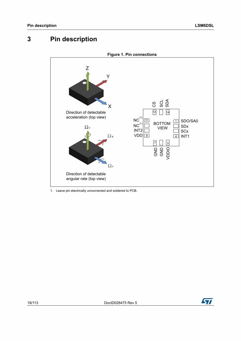
3 Pin description
Figure 1. Pin connections
1. Leave pin electrically unconnected and soldered to PCB.
ΩΩ Y
Ω R
Ω P
Z
Y
X
NCNC
(1)
(1)
DocID028475 Rev 5 19/113
LSM6DSL Pin description
113
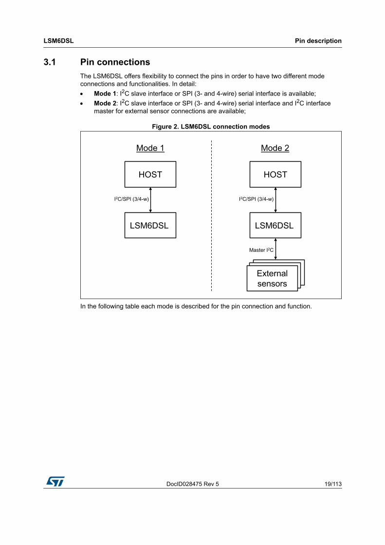
3.1 Pin connectionsThe LSM6DSL offers flexibility to connect the pins in order to have two different mode connections and functionalities. In detail: Mode 1: I2C slave interface or SPI (3- and 4-wire) serial interface is available; Mode 2: I2C slave interface or SPI (3- and 4-wire) serial interface and I2C interface
master for external sensor connections are available;
Figure 2. LSM6DSL connection modes
In the following table each mode is described for the pin connection and function.
Pin description LSM6DSL
20/113 DocID028475 Rev 5
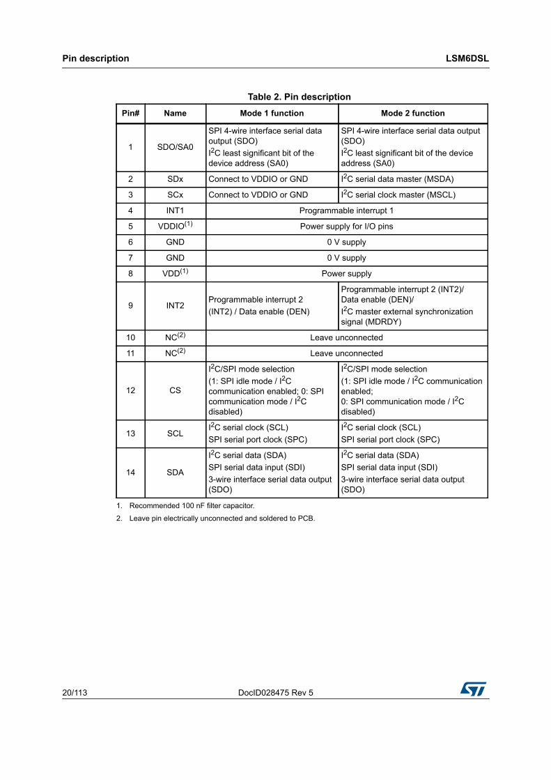
Table 2. Pin description Pin# Name Mode 1 function Mode 2 function
1 SDO/SA0
SPI 4-wire interface serial data output (SDO)I2C least significant bit of the device address (SA0)
SPI 4-wire interface serial data output (SDO)I2C least significant bit of the device address (SA0)
2 SDx Connect to VDDIO or GND I2C serial data master (MSDA)
3 SCx Connect to VDDIO or GND I2C serial clock master (MSCL)
4 INT1 Programmable interrupt 1
5 VDDIO(1)
1. Recommended 100 nF filter capacitor.
Power supply for I/O pins
6 GND 0 V supply
7 GND 0 V supply
8 VDD(1) Power supply
9 INT2Programmable interrupt 2(INT2) / Data enable (DEN)
Programmable interrupt 2 (INT2)/ Data enable (DEN)/I2C master external synchronization signal (MDRDY)
10 NC(2)
2. Leave pin electrically unconnected and soldered to PCB.
Leave unconnected
11 NC(2) Leave unconnected
12 CS
I2C/SPI mode selection (1: SPI idle mode / I2C communication enabled; 0: SPI communication mode / I2C disabled)
I2C/SPI mode selection (1: SPI idle mode / I2C communication enabled; 0: SPI communication mode / I2C disabled)
13 SCLI2C serial clock (SCL)SPI serial port clock (SPC)
I2C serial clock (SCL)SPI serial port clock (SPC)
14 SDA
I2C serial data (SDA)SPI serial data input (SDI)3-wire interface serial data output (SDO)
I2C serial data (SDA)SPI serial data input (SDI)3-wire interface serial data output (SDO)
DocID028475 Rev 5 21/113
LSM6DSL Module specifications
113
4 Module specifications
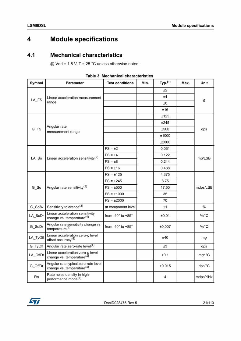
4.1 Mechanical characteristics@ Vdd = 1.8 V, T = 25 °C unless otherwise noted.
Table 3. Mechanical characteristics Symbol Parameter Test conditions Min. Typ.(1) Max. Unit
LA_FS Linear acceleration measurement range
±2
g±4
±8
±16
G_FSAngular ratemeasurement range
±125
dps
±245
±500
±1000
±2000
LA_So Linear acceleration sensitivity(2)
FS = ±2 0.061
mg/LSBFS = ±4 0.122
FS = ±8 0.244
FS = ±16 0.488
G_So Angular rate sensitivity(2)
FS = ±125 4.375
mdps/LSB
FS = ±245 8.75
FS = ±500 17.50
FS = ±1000 35
FS = ±2000 70
G_So% Sensitivity tolerance(3) at component level ±1 %
LA_SoDr Linear acceleration sensitivity change vs. temperature(4) from -40° to +85° ±0.01 %/°C
G_SoDr Angular rate sensitivity change vs. temperature(4) from -40° to +85° ±0.007 %/°C
LA_TyOff Linear acceleration zero-g level offset accuracy(5) ±40 mg
G_TyOff Angular rate zero-rate level(4) ±3 dps
LA_OffDr Linear acceleration zero-g level change vs. temperature(4) ±0.1 mg/ °C
G_OffDr Angular rate typical zero-rate level change vs. temperature(4) ±0.015 dps/°C
Rn Rate noise density in high-performance mode(6) 4 mdps/Hz
Module specifications LSM6DSL
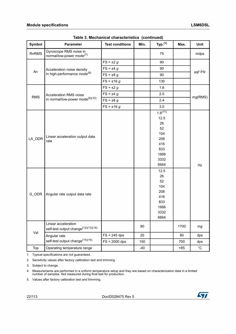
22/113 DocID028475 Rev 5
RnRMS Gyroscope RMS noise in normal/low-power mode(7) 75 mdps
An Acceleration noise density in high-performance mode(8)
FS = ±2 g 90
μg/√HzFS = ±4 g 90
FS = ±8 g 90
FS = ±16 g 130
RMS Acceleration RMS noise in normal/low-power mode(9)(10)
FS = ±2 g 1.8
mg(RMS)FS = ±4 g 2.0
FS = ±8 g 2.4
FS = ±16 g 3.0
LA_ODR Linear acceleration output data rate
1.6(11)
12.52652104208416833166633326664 Hz
G_ODR Angular rate output data rate
12.52652104208416833166633326664
Vst
Linear accelerationself-test output change(12)(13)(14) 90 1700 mg
Angular rateself-test output change(15)(16)
FS = 245 dps 20 80 dps
FS = 2000 dps 150 700 dps
Top Operating temperature range -40 +85 °C
1. Typical specifications are not guaranteed.
2. Sensitivity values after factory calibration test and trimming
3. Subject to change.
4. Measurements are performed in a uniform temperature setup and they are based on characterization data in a limited number of samples. Not measured during final test for production.
5. Values after factory calibration test and trimming.
Table 3. Mechanical characteristics (continued)Symbol Parameter Test conditions Min. Typ.(1) Max. Unit
DocID028475 Rev 5 23/113
LSM6DSL Module specifications
113
6. Gyroscope rate noise density in high-performance mode is independent of the ODR and FS setting.
7. Gyroscope RMS noise in normal/low-power mode is independent of the ODR and FS setting.
8. Accelerometer noise density in high-performance mode is independent of the ODR.
9. Accelerometer RMS noise in normal/low-power mode is independent of the ODR.
10. Noise RMS related to BW = ODR /2 (for ODR /9, typ value can be calculated by Typ *0.6).
11. This ODR is available when accelerometer is in low-power mode.
12. The sign of the linear acceleration self-test output change is defined by the STx_XL bits in CTRL5_C (14h), Table 63 for all axes.
13. The linear acceleration self-test output change is defined with the device in stationary condition as the absolute value of:OUTPUT[LSb] (self-test enabled) - OUTPUT[LSb] (self-test disabled). 1LSb = 0.061 mg at ±2 g full scale.
14. Accelerometer self-test limits are full-scale independent.
15. The sign of the angular rate self-test output change is defined by the STx_G bits in CTRL5_C (14h), Table 62 for all axes.
16. The angular rate self-test output change is defined with the device in stationary condition as the absolute value of:OUTPUT[LSb] (self-test enabled) - OUTPUT[LSb] (self-test disabled). 1LSb = 70 mdps at ±2000 dps full scale.
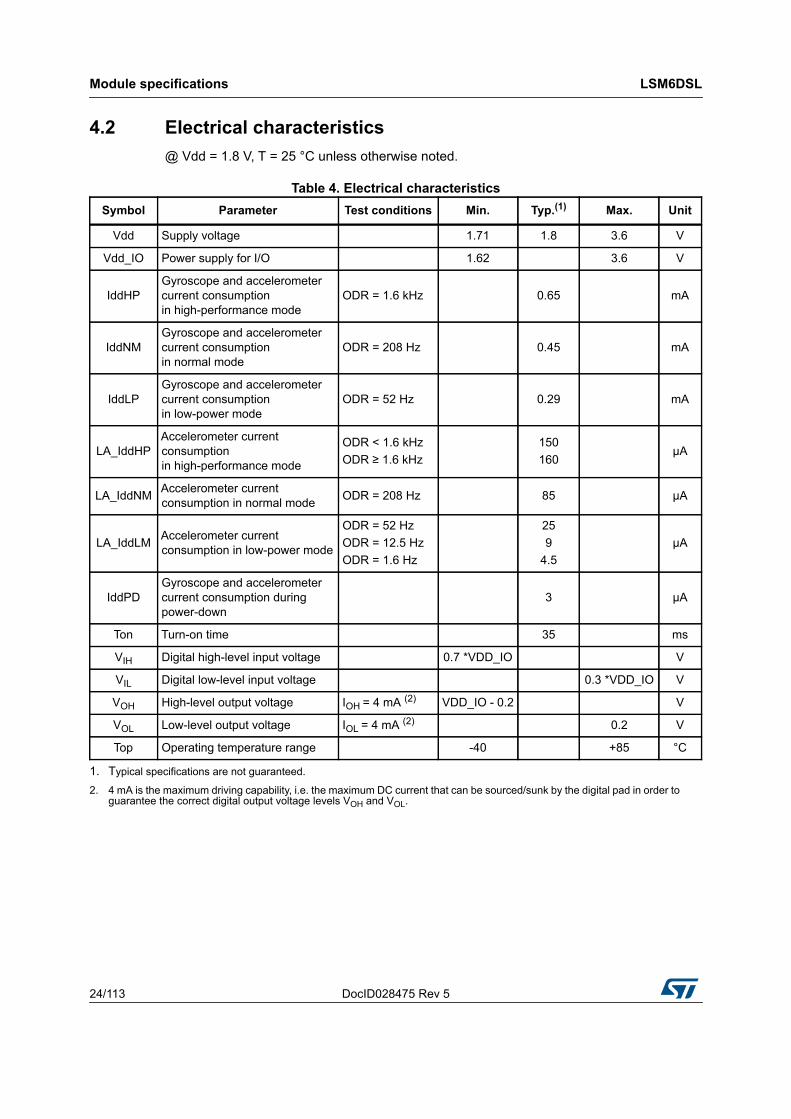
Module specifications LSM6DSL
24/113 DocID028475 Rev 5
4.2 Electrical characteristics@ Vdd = 1.8 V, T = 25 °C unless otherwise noted.
Table 4. Electrical characteristicsSymbol Parameter Test conditions Min. Typ.(1)
1. Typical specifications are not guaranteed.
Max. Unit
Vdd Supply voltage 1.71 1.8 3.6 V
Vdd_IO Power supply for I/O 1.62 3.6 V
IddHPGyroscope and accelerometer current consumption in high-performance mode
ODR = 1.6 kHz 0.65 mA
IddNMGyroscope and accelerometer current consumption in normal mode
ODR = 208 Hz 0.45 mA
IddLPGyroscope and accelerometer current consumption in low-power mode
ODR = 52 Hz 0.29 mA
LA_IddHPAccelerometer current consumption in high-performance mode
ODR < 1.6 kHzODR ≥ 1.6 kHz
150160
μA
LA_IddNM Accelerometer current consumption in normal mode ODR = 208 Hz 85 μA
LA_IddLM Accelerometer current consumption in low-power mode
ODR = 52 HzODR = 12.5 HzODR = 1.6 Hz
259
4.5μA
IddPDGyroscope and accelerometer current consumption during power-down
3 μA
Ton Turn-on time 35 ms
VIH Digital high-level input voltage 0.7 *VDD_IO V
VIL Digital low-level input voltage 0.3 *VDD_IO V
VOH High-level output voltage IOH = 4 mA (2)
2. 4 mA is the maximum driving capability, i.e. the maximum DC current that can be sourced/sunk by the digital pad in order to guarantee the correct digital output voltage levels VOH and VOL.
VDD_IO - 0.2 V
VOL Low-level output voltage IOL = 4 mA (2) 0.2 V
Top Operating temperature range -40 +85 °C

DocID028475 Rev 5 25/113
LSM6DSL Module specifications
113
4.3 Temperature sensor characteristics@ Vdd = 1.8 V, T = 25 °C unless otherwise noted.
Table 5. Temperature sensor characteristicsSymbol Parameter Test condition Min. Typ.(1)
1. Typical specifications are not guaranteed.
Max. Unit
TODR(2)
2. When the accelerometer is in Low-Power mode and the gyroscope part is turned off, the TODR value is equal to the accelerometer ODR.
Temperature refresh rate 52 Hz
Toff Temperature offset(3)
3. The output of the temperature sensor is 0 LSB (typ.) at 25 °C.
-15 +15 °C
TSen Temperature sensitivity 256 LSB/°C
TST Temperature stabilization time(4)
4. Time from power ON bit to valid data based on characterization data.
500 μs
T_ADC_res Temperature ADC resolution 16 bit
Top Operating temperature range -40 +85 °C

Module specifications LSM6DSL
26/113 DocID028475 Rev 5
4.4 Communication interface characteristics
4.4.1 SPI - serial peripheral interfaceSubject to general operating conditions for Vdd and Top.
Figure 3. SPI slave timing diagram
Note: Measurement points are done at 0.2·Vdd_IO and 0.8·Vdd_IO, for both input and output ports.
Table 6. SPI slave timing values
Symbol ParameterValue(1)
UnitMin Max
tc(SPC) SPI clock cycle 100 ns
fc(SPC) SPI clock frequency 10 MHz
tsu(CS) CS setup time 5
ns
th(CS) CS hold time 20
tsu(SI) SDI input setup time 5
th(SI) SDI input hold time 15
tv(SO) SDO valid output time 50
th(SO) SDO output hold time 5
tdis(SO) SDO output disable time 50
1. Values are guaranteed at 10 MHz clock frequency for SPI with both 4 and 3 wires, based on characterization results, not tested in production
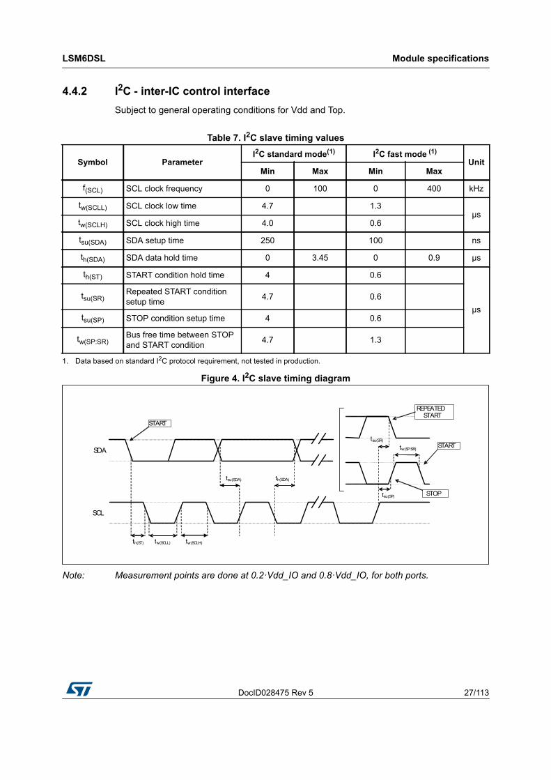
DocID028475 Rev 5 27/113
LSM6DSL Module specifications
113
4.4.2 I2C - inter-IC control interfaceSubject to general operating conditions for Vdd and Top.
Figure 4. I2C slave timing diagram
Note: Measurement points are done at 0.2·Vdd_IO and 0.8·Vdd_IO, for both ports.
Table 7. I2C slave timing values
Symbol ParameterI2C standard mode(1) I2C fast mode (1)
UnitMin Max Min Max
f(SCL) SCL clock frequency 0 100 0 400 kHz
tw(SCLL) SCL clock low time 4.7 1.3μs
tw(SCLH) SCL clock high time 4.0 0.6
tsu(SDA) SDA setup time 250 100 ns
th(SDA) SDA data hold time 0 3.45 0 0.9 μs
th(ST) START condition hold time 4 0.6
μstsu(SR)
Repeated START condition setup time 4.7 0.6
tsu(SP) STOP condition setup time 4 0.6
tw(SP:SR)Bus free time between STOP and START condition 4.7 1.3
1. Data based on standard I2C protocol requirement, not tested in production.
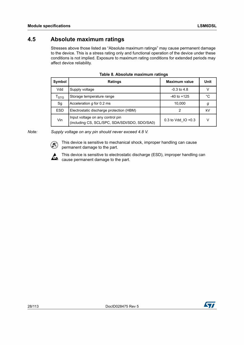
Module specifications LSM6DSL
28/113 DocID028475 Rev 5
4.5 Absolute maximum ratingsStresses above those listed as “Absolute maximum ratings” may cause permanent damage to the device. This is a stress rating only and functional operation of the device under these conditions is not implied. Exposure to maximum rating conditions for extended periods may affect device reliability.
Note: Supply voltage on any pin should never exceed 4.8 V.
Table 8. Absolute maximum ratingsSymbol Ratings Maximum value Unit
Vdd Supply voltage -0.3 to 4.8 V
TSTG Storage temperature range -40 to +125 °C
Sg Acceleration g for 0.2 ms 10,000 g
ESD Electrostatic discharge protection (HBM) 2 kV
VinInput voltage on any control pin(including CS, SCL/SPC, SDA/SDI/SDO, SDO/SA0)
0.3 to Vdd_IO +0.3 V
This device is sensitive to mechanical shock, improper handling can cause permanent damage to the part.
This device is sensitive to electrostatic discharge (ESD), improper handling can cause permanent damage to the part.
DocID028475 Rev 5 29/113
LSM6DSL Module specifications
113
4.6 Terminology
4.6.1 SensitivityLinear acceleration sensitivity can be determined, for example, by applying 1 g acceleration to the device. Because the sensor can measure DC accelerations, this can be done easily by pointing the selected axis towards the ground, noting the output value, rotating the sensor 180 degrees (pointing towards the sky) and noting the output value again. By doing so, ±1 g acceleration is applied to the sensor. Subtracting the larger output value from the smaller one, and dividing the result by 2, leads to the actual sensitivity of the sensor. This value changes very little over temperature and over time. The sensitivity tolerance describes the range of sensitivities of a large number of sensors (see Table 3).
An angular rate gyroscope is a device that produces a positive-going digital output for counterclockwise rotation around the axis considered. Sensitivity describes the gain of the sensor and can be determined by applying a defined angular velocity to it. This value changes very little over temperature and time (see Table 3).
4.6.2 Zero-g and zero-rate levelLinear acceleration zero-g level offset (TyOff) describes the deviation of an actual output signal from the ideal output signal if no acceleration is present. A sensor in a steady state on a horizontal surface will measure 0 g on both the X-axis and Y-axis, whereas the Z-axis will measure 1 g. Ideally, the output is in the middle of the dynamic range of the sensor (content of OUT registers 00h, data expressed as 2’s complement number). A deviation from the ideal value in this case is called zero-g offset.
Offset is to some extent a result of stress to MEMS sensor and therefore the offset can slightly change after mounting the sensor onto a printed circuit board or exposing it to extensive mechanical stress. Offset changes little over temperature, see “Linear acceleration zero-g level change vs. temperature” in Table 3. The zero-g level tolerance (TyOff) describes the standard deviation of the range of zero-g levels of a group of sensors.
Zero-rate level describes the actual output signal if there is no angular rate present. The zero-rate level of precise MEMS sensors is, to some extent, a result of stress to the sensor and therefore the zero-rate level can slightly change after mounting the sensor onto a printed circuit board or after exposing it to extensive mechanical stress. This value changes very little over temperature and time (see Table 3).
Functionality LSM6DSL
30/113 DocID028475 Rev 5
5 Functionality
5.1 Operating modesIn the LSM6DSL, the accelerometer and the gyroscope can be turned on/off independently of each other and are allowed to have different ODRs and power modes.
The LSM6DSL has three operating modes available: only accelerometer active and gyroscope in power-down only gyroscope active and accelerometer in power-down both accelerometer and gyroscope sensors active with independent ODR
The accelerometer is activated from power-down by writing ODR_XL[3:0] in CTRL1_XL (10h) while the gyroscope is activated from power-down by writing ODR_G[3:0] in CTRL2_G (11h). For combo-mode the ODRs are totally independent.
5.2 Gyroscope power modesIn the LSM6DSL, the gyroscope can be configured in four different operating modes: power-down, low-power, normal mode and high-performance mode. The operating mode selected depends on the value of the G_HM_MODE bit in CTRL7_G (16h). If G_HM_MODE is set to '0', high-performance mode is valid for all ODRs (from 12.5 Hz up to 6.66 kHz).
To enable the low-power and normal mode, the G_HM_MODE bit has to be set to '1'. Low-power mode is available for lower ODRs (12.5, 26, 52 Hz) while normal mode is available for ODRs equal to 104 and 208 Hz.
5.3 Accelerometer power modesIn the LSM6DSL, the accelerometer can be configured in four different operating modes: power-down, low-power, normal mode and high-performance mode. The operating mode selected depends on the value of the XL_HM_MODE bit in CTRL6_C (15h). If XL_HM_MODE is set to '0', high-performance mode is valid for all ODRs (from 12.5 Hz up to 6.66 kHz).
To enable the low-power and normal mode, the XL_HM_MODE bit has to be set to '1'. Low-power mode is available for lower ODRs (1.6, 12.5, 26, 52 Hz) while normal mode is available for ODRs equal to 104 and 208 Hz.
DocID028475 Rev 5 31/113
LSM6DSL Functionality
113
5.4 Block diagram of filters
Figure 5. Block diagram of filters
5.4.1 Block diagrams of the gyroscope filtersThe gyroscope filtering configuration for both Mode 1 (for User Interface (UI) and Electronic Image Stabilization (EIS) functionality) and Mode 2 is shown in Figure 6.
Figure 6. Gyroscope digital chain - Mode 1 (UI/EIS) and Mode 2
The gyroscope ODR is selectable from 12.5 Hz up to 6.66 kHz. A low-pass filter (LPF1) is available, for more details about the filter characteristics see Table 67: Gyroscope LPF1 bandwidth selection.
Data can be acquired from the output registers and FIFO over the I2C/SPI interface.

Functionality LSM6DSL
32/113 DocID028475 Rev 5
5.4.2 Block diagrams of the accelerometer filtersIn the LSM6DSL, the filtering chain for the accelerometer part is composed of the following: Analog filter (anti-aliasing) Digital filter (LPF1) Composite filter
Details of the block diagram appear in the following figure.
Figure 7. Accelerometer chain
The configuration of the digital filter can be set using the LPF1_BW_SEL bit in CTRL1_XL (10h) and the INPUT_COMPOSITE bit in CTRL8_XL (17h).
Figure 8. Accelerometer composite filter
1. Pedometer, step detector and step counter, significant motion and tilt functions.

DocID028475 Rev 5 33/113
LSM6DSL Functionality
113
5.5 FIFOThe presence of a FIFO allows consistent power saving for the system since the host processor does not need continuously poll data from the sensor, but it can wake up only when needed and burst the significant data out from the FIFO.
The LSM6DSL embeds 4 kbytes data FIFO to store the following data: gyroscope accelerometer external sensors step counter and timestamp temperature
Writing data in the FIFO can be configured to be triggered by the: accelerometer/gyroscope data-ready signal; in which case the ODR must be lower
than or equal to both the accelerometer and gyroscope ODRs; sensor hub data-ready signal; step detection signal.
In addition, each data can be stored at a decimated data rate compared to FIFO ODR and it is configurable by the user, setting the FIFO_CTRL3 (08h) and FIFO_CTRL4 (09h) registers. The available decimation factors are 2, 3, 4, 8, 16, 32.
The programmable FIFO threshold can be set in FIFO_CTRL1 (06h) and FIFO_CTRL2 (07h) using the FTH [11:0] bits.
To monitor the FIFO status, dedicated registers FIFO_STATUS1 (3Ah), FIFO_STATUS2 (3Bh), FIFO_STATUS3 (3Ch), FIFO_STATUS4 (3Dh)) can be read to detect FIFO overrun events, FIFO full status, FIFO empty status, FIFO threshold status and the number of unread samples stored in the FIFO. To generate dedicated interrupts on the INT1 and INT2 pads of these status events, the configuration can be set in INT1_CTRL (0Dh) and INT2_CTRL (0Eh).
The FIFO buffer can be configured according to five different modes: Bypass mode FIFO mode Continuous mode Continuous-to-FIFO mode Bypass-to-continuous mode
Each mode is selected by the FIFO_MODE_[2:0] bits in the FIFO_CTRL5 (0Ah) register. To guarantee the correct acquisition of data during the switching into and out of FIFO mode, the first sample acquired must be discarded.
5.5.1 Bypass modeIn Bypass mode (FIFO_CTRL5 (0Ah) (FIFO_MODE_[2:0] = 000), the FIFO is not operational and it remains empty.
Bypass mode is also used to reset the FIFO when in FIFO mode.
Functionality LSM6DSL
34/113 DocID028475 Rev 5
5.5.2 FIFO modeIn FIFO mode (FIFO_CTRL5 (0Ah) (FIFO_MODE_[2:0] = 001) data from the output channels are stored in the FIFO until it is full.
To reset FIFO content, Bypass mode should be selected by writing FIFO_CTRL5 (0Ah) (FIFO_MODE_[2:0]) to '000' After this reset command, it is possible to restart FIFO mode by writing FIFO_CTRL5 (0Ah)(FIFO_MODE_[2:0]) to '001'.
FIFO buffer memorizes up to 4096 samples of 16 bits each but the depth of the FIFO can be resized by setting the FTH [11:0] bits in FIFO_CTRL1 (06h) and FIFO_CTRL2 (07h). If the STOP_ON_FTH bit in CTRL4_C (13h) is set to '1', FIFO depth is limited up to FTH [11:0] bits in FIFO_CTRL1 (06h) and FIFO_CTRL2 (07h).
5.5.3 Continuous mode Continuous mode (FIFO_CTRL5 (0Ah) (FIFO_MODE_[2:0] = 110) provides a continuous FIFO update: as new data arrives, the older data is discarded.
A FIFO threshold flag FIFO_STATUS2 (3Bh)(FTH) is asserted when the number of unread samples in FIFO is greater than or equal to FIFO_CTRL1 (06h) and FIFO_CTRL2 (07h)(FTH [11:0]).
It is possible to route FIFO_STATUS2 (3Bh)(FTH) to the INT1 pin by writing in register INT1_CTRL (0Dh)(INT1_FTH) = ‘1’ or to the INT2 pin by writing in register INT2_CTRL (0Eh)(INT2_FTH) = ‘1’.
A full-flag interrupt can be enabled, INT1_CTRL (0Dh)(INT_ FULL_FLAG) = '1', in order to indicate FIFO saturation and eventually read its content all at once.
If an overrun occurs, at least one of the oldest samples in FIFO has been overwritten and the OVER_RUN flag in FIFO_STATUS2 (3Bh) is asserted.
In order to empty the FIFO before it is full, it is also possible to pull from FIFO the number of unread samples available in FIFO_STATUS1 (3Ah) and FIFO_STATUS2 (3Bh) (DIFF_FIFO[11:0]).
5.5.4 Continuous-to-FIFO modeIn Continuous-to-FIFO mode FIFO_CTRL5 (0Ah)(FIFO_MODE_[2:0] = 011), FIFO behavior changes according to the trigger event detected in one of the following interrupt registers FUNC_SRC1 (53h), TAP_SRC (1Ch), WAKE_UP_SRC (1Bh) and D6D_SRC (1Dh).
When the selected trigger bit is equal to '1', FIFO operates in FIFO mode.
When the selected trigger bit is equal to '0', FIFO operates in Continuous mode.
5.5.5 Bypass-to-Continuous mode In Bypass-to-Continuous mode (FIFO_CTRL5 (0Ah) (FIFO_MODE_[2:0] = '100'), data measurement storage inside FIFO operates in Continuous mode when selected triggers in one of the following interrupt registers FUNC_SRC1 (53h), TAP_SRC (1Ch), WAKE_UP_SRC (1Bh)and D6D_SRC (1Dh) are equal to '1', otherwise FIFO content is reset (Bypass mode).
DocID028475 Rev 5 35/113
LSM6DSL Functionality
113
5.5.6 FIFO reading procedureThe data stored in FIFO are accessible from dedicated registers (FIFO_DATA_OUT_L (3Eh) and FIFO_DATA_OUT_H (3Fh)) and each FIFO sample is composed of 16 bits.
All FIFO status registers (FIFO_STATUS1 (3Ah), FIFO_STATUS2 (3Bh), FIFO_STATUS3 (3Ch), FIFO_STATUS4 (3Dh)) can be read at the start of a reading operation, minimizing the intervention of the application processor.
Saving data in the FIFO buffer is organized in four FIFO data sets consisting of 6 bytes each:
The 1st FIFO data set is reserved for gyroscope data;
The 2nd FIFO data set is reserved for accelerometer data;
The 3rd FIFO data set is reserved for the external sensor data stored in the registers from SENSORHUB1_REG (2Eh) to SENSORHUB6_REG (33h);
The 4th FIFO data set can be alternately associated to the external sensor data stored in the registers from SENSORHUB7_REG (34h) to SENSORHUB12_REG (39h), to the step counter and timestamp info, or to the temperature sensor data.
Digital interfaces LSM6DSL
36/113 DocID028475 Rev 5
6 Digital interfaces
6.1 I2C/SPI interfaceThe registers embedded inside the LSM6DSL may be accessed through both the I2C and SPI serial interfaces. The latter may be SW configured to operate either in 3-wire or 4-wire interface mode.
The serial interfaces are mapped onto the same pins. To select/exploit the I2C interface, the CS line must be tied high (i.e connected to Vdd_IO).
6.2 Master I2CIf the LSM6DSL is configured in Mode2, a master I2C line is available. The master serial interface is mapped in the following dedicated pins.
Table 9. Serial interface pin descriptionPin name Pin description
CSSPI enableI2C/SPI mode selection (1: SPI idle mode / I2C communication enabled; 0: SPI communication mode / I2C disabled)
SCL/SPCI2C Serial Clock (SCL)SPI Serial Port Clock (SPC)
SDA/SDI/SDOI2C Serial Data (SDA)SPI Serial Data Input (SDI)3-wire Interface Serial Data Output (SDO)
SDO/SA0SPI Serial Data Output (SDO)I2C less significant bit of the device address
Table 10. Master I2C pin detailsPin name Pin description
MSCL I2C serial clock master
MSDA I2C serial data master
MDRDY I2C master external synchronization signal
DocID028475 Rev 5 37/113
LSM6DSL Digital interfaces
113
6.3 I2C serial interfaceThe LSM6DSL I2C is a bus slave. The I2C is employed to write the data to the registers, whose content can also be read back.
The relevant I2C terminology is provided in the table below.
There are two signals associated with the I2C bus: the serial clock line (SCL) and the Serial DAta line (SDA). The latter is a bidirectional line used for sending and receiving the data to/from the interface. Both the lines must be connected to Vdd_IO through external pull-up resistors. When the bus is free, both the lines are high.
The I2C interface is implemeted with fast mode (400 kHz) I2C standards as well as with the standard mode.
In order to disable the I2C block, (I2C_disable) = 1 must be written in CTRL4_C (13h).
6.3.1 I2C operationThe transaction on the bus is started through a START (ST) signal. A START condition is defined as a HIGH to LOW transition on the data line while the SCL line is held HIGH. After this has been transmitted by the master, the bus is considered busy. The next byte of data transmitted after the start condition contains the address of the slave in the first 7 bits and the eighth bit tells whether the master is receiving data from the slave or transmitting data to the slave. When an address is sent, each device in the system compares the first seven bits after a start condition with its address. If they match, the device considers itself addressed by the master.
The Slave ADdress (SAD) associated to the LSM6DSL is 110101xb. The SDO/SA0 pin can be used to modify the less significant bit of the device address. If the SDO/SA0 pin is connected to the supply voltage, LSb is ‘1’ (address 1101011b); else if the SDO/SA0 pin is connected to ground, the LSb value is ‘0’ (address 1101010b). This solution permits to connect and address two different inertial modules to the same I2C bus.
Data transfer with acknowledge is mandatory. The transmitter must release the SDA line during the acknowledge pulse. The receiver must then pull the data line LOW so that it remains stable low during the HIGH period of the acknowledge clock pulse. A receiver which has been addressed is obliged to generate an acknowledge after each byte of data received.
The I2C embedded inside the LSM6DSL behaves like a slave device and the following protocol must be adhered to. After the start condition (ST) a slave address is sent, once a slave acknowledge (SAK) has been returned, an 8-bit sub-address (SUB) is transmitted. The increment of the address is configured by the CTRL3_C (12h) (IF_INC).
Table 11. I2C terminologyTerm Description
Transmitter The device which sends data to the bus
Receiver The device which receives data from the bus
Master The device which initiates a transfer, generates clock signals and terminates a transfer
Slave The device addressed by the master

Digital interfaces LSM6DSL
38/113 DocID028475 Rev 5
The slave address is completed with a Read/Write bit. If the bit is ‘1’ (Read), a repeated START (SR) condition must be issued after the two sub-address bytes; if the bit is ‘0’ (Write) the master will transmit to the slave with direction unchanged. Table 12 explains how the SAD+Read/Write bit pattern is composed, listing all the possible configurations.
Table 12. SAD+Read/Write patterns
Data are transmitted in byte format (DATA). Each data transfer contains 8 bits. The number of bytes transferred per transfer is unlimited. Data is transferred with the Most Significant bit (MSb) first. If a receiver can’t receive another complete byte of data until it has performed some other function, it can hold the clock line, SCL LOW to force the transmitter into a wait state. Data transfer only continues when the receiver is ready for another byte and releases the data line. If a slave receiver doesn’t acknowledge the slave address (i.e. it is not able to receive because it is performing some real-time function) the data line must be left HIGH by the slave. The master can then abort the transfer. A LOW to HIGH transition on the SDA line while the SCL line is HIGH is defined as a STOP condition. Each data transfer must be terminated by the generation of a STOP (SP) condition.
In the presented communication format MAK is Master acknowledge and NMAK is No Master Acknowledge.
Command SAD[6:1] SAD[0] = SA0 R/W SAD+R/W
Read 110101 0 1 11010101 (D5h)
Write 110101 0 0 11010100 (D4h)
Read 110101 1 1 11010111 (D7h)
Write 110101 1 0 11010110 (D6h)
Table 13. Transfer when master is writing one byte to slaveMaster ST SAD + W SUB DATA SP
Slave SAK SAK SAK
Table 14. Transfer when master is writing multiple bytes to slaveMaster ST SAD + W SUB DATA DATA SP
Slave SAK SAK SAK SAK
Table 15. Transfer when master is receiving (reading) one byte of data from slaveMaster ST SAD + W SUB SR SAD + R NMAK SP
Slave SAK SAK SAK DATA
Table 16. Transfer when master is receiving (reading) multiple bytes of data from slaveMaster ST SAD+W SUB SR SAD+R MAK MAK NMAK SP
Slave SAK SAK SAK DATA DATA DATA
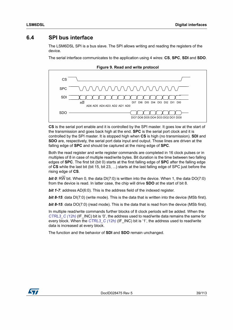
DocID028475 Rev 5 39/113
LSM6DSL Digital interfaces
113
6.4 SPI bus interfaceThe LSM6DSL SPI is a bus slave. The SPI allows writing and reading the registers of the device.
The serial interface communicates to the application using 4 wires: CS, SPC, SDI and SDO.
Figure 9. Read and write protocol
CS is the serial port enable and it is controlled by the SPI master. It goes low at the start of the transmission and goes back high at the end. SPC is the serial port clock and it is controlled by the SPI master. It is stopped high when CS is high (no transmission). SDI and SDO are, respectively, the serial port data input and output. Those lines are driven at the falling edge of SPC and should be captured at the rising edge of SPC.
Both the read register and write register commands are completed in 16 clock pulses or in multiples of 8 in case of multiple read/write bytes. Bit duration is the time between two falling edges of SPC. The first bit (bit 0) starts at the first falling edge of SPC after the falling edge of CS while the last bit (bit 15, bit 23, ...) starts at the last falling edge of SPC just before the rising edge of CS.
bit 0: RW bit. When 0, the data DI(7:0) is written into the device. When 1, the data DO(7:0) from the device is read. In latter case, the chip will drive SDO at the start of bit 8.
bit 1-7: address AD(6:0). This is the address field of the indexed register.
bit 8-15: data DI(7:0) (write mode). This is the data that is written into the device (MSb first).
bit 8-15: data DO(7:0) (read mode). This is the data that is read from the device (MSb first).
In multiple read/write commands further blocks of 8 clock periods will be added. When the CTRL3_C (12h) (IF_INC) bit is ‘0’, the address used to read/write data remains the same for every block. When the CTRL3_C (12h) (IF_INC) bit is ‘1’, the address used to read/write data is increased at every block.
The function and the behavior of SDI and SDO remain unchanged.
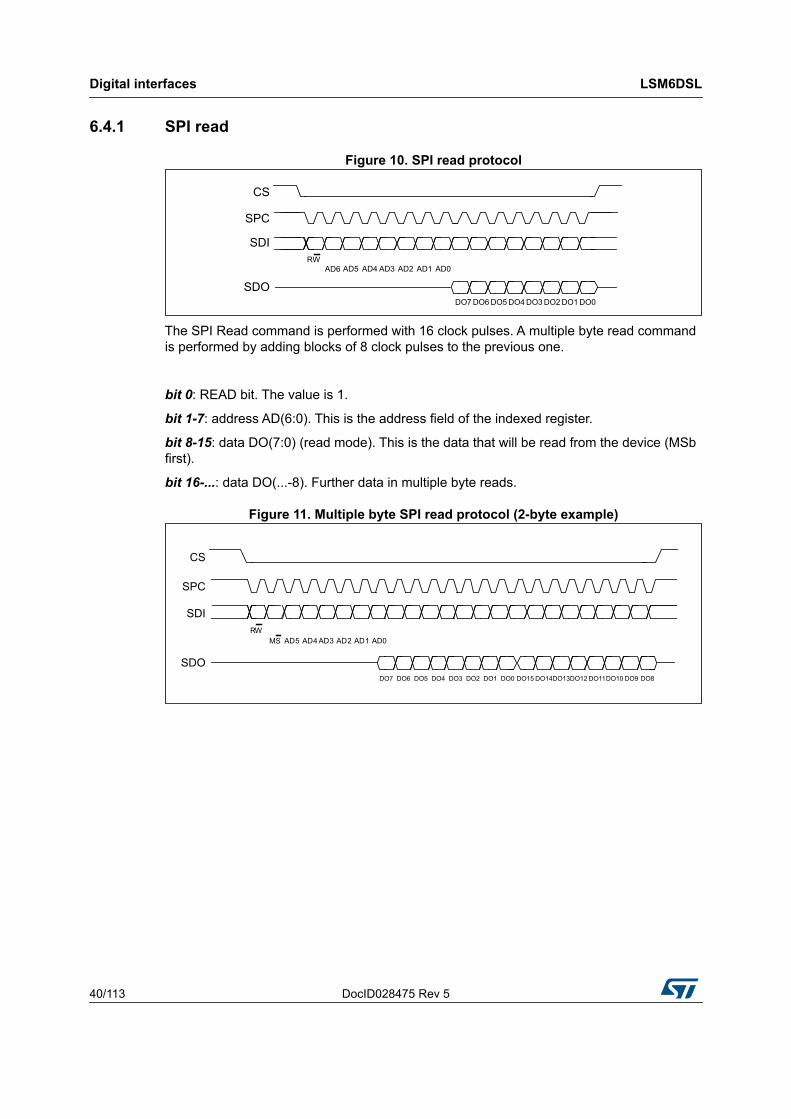
Digital interfaces LSM6DSL
40/113 DocID028475 Rev 5
6.4.1 SPI read
Figure 10. SPI read protocol
The SPI Read command is performed with 16 clock pulses. A multiple byte read command is performed by adding blocks of 8 clock pulses to the previous one.
bit 0: READ bit. The value is 1.
bit 1-7: address AD(6:0). This is the address field of the indexed register.
bit 8-15: data DO(7:0) (read mode). This is the data that will be read from the device (MSb first).
bit 16-...: data DO(...-8). Further data in multiple byte reads.
Figure 11. Multiple byte SPI read protocol (2-byte example)
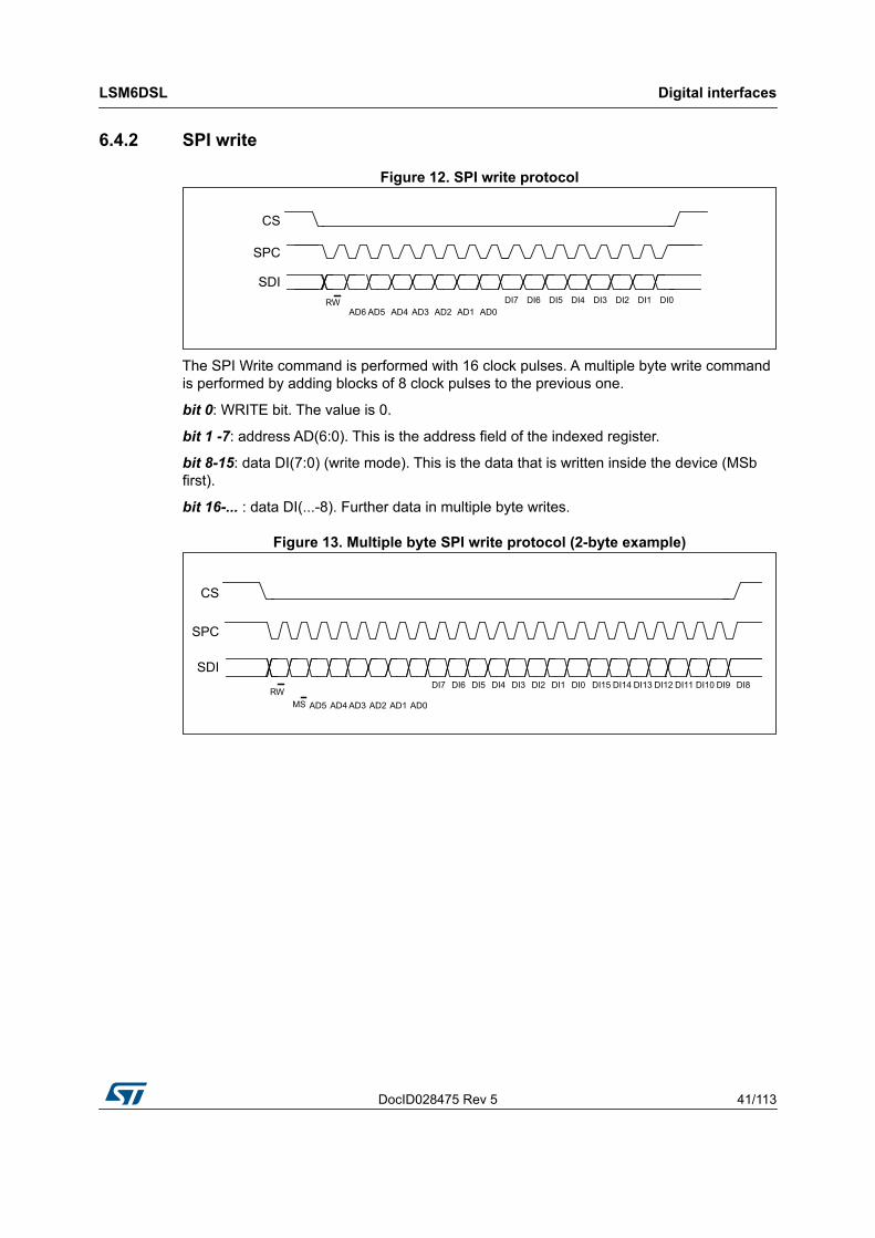
DocID028475 Rev 5 41/113
LSM6DSL Digital interfaces
113
6.4.2 SPI write
Figure 12. SPI write protocol
The SPI Write command is performed with 16 clock pulses. A multiple byte write command is performed by adding blocks of 8 clock pulses to the previous one.
bit 0: WRITE bit. The value is 0.
bit 1 -7: address AD(6:0). This is the address field of the indexed register.
bit 8-15: data DI(7:0) (write mode). This is the data that is written inside the device (MSb first).
bit 16-... : data DI(...-8). Further data in multiple byte writes.
Figure 13. Multiple byte SPI write protocol (2-byte example)

Digital interfaces LSM6DSL
42/113 DocID028475 Rev 5
6.4.3 SPI read in 3-wire modeA 3-wire mode is entered by setting the CTRL3_C (12h) (SIM) bit equal to ‘1’ (SPI serial interface mode selection).
Figure 14. SPI read protocol in 3-wire mode
The SPI read command is performed with 16 clock pulses:
bit 0: READ bit. The value is 1.
bit 1-7: address AD(6:0). This is the address field of the indexed register.
bit 8-15: data DO(7:0) (read mode). This is the data that is read from the device (MSb first).
A multiple read command is also available in 3-wire mode.

DocID028475 Rev 5 43/113
LSM6DSL Application hints
113
7 Application hints
7.1 LSM6DSL electrical connections in Mode 1
Figure 15. LSM6DSL electrical connections in Mode 1
1. Leave pin electrically unconnected and soldered to PCB.
The device core is supplied through the Vdd line. Power supply decoupling capacitors (C1, C2 = 100 nF ceramic) should be placed as near as possible to the supply pin of the device (common design practice).
The functionality of the device and the measured acceleration/angular rate data is selectable and accessible through the SPI/I2C interface.
The functions, the threshold and the timing of the two interrupt pins for each sensor can be completely programmed by the user through the SPI/I2C interface.
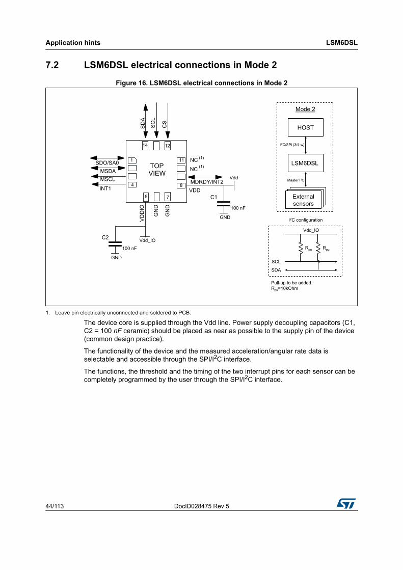
Application hints LSM6DSL
44/113 DocID028475 Rev 5
7.2 LSM6DSL electrical connections in Mode 2
Figure 16. LSM6DSL electrical connections in Mode 2
1. Leave pin electrically unconnected and soldered to PCB.
The device core is supplied through the Vdd line. Power supply decoupling capacitors (C1, C2 = 100 nF ceramic) should be placed as near as possible to the supply pin of the device (common design practice).
The functionality of the device and the measured acceleration/angular rate data is selectable and accessible through the SPI/I2C interface.
The functions, the threshold and the timing of the two interrupt pins for each sensor can be completely programmed by the user through the SPI/I2C interface.
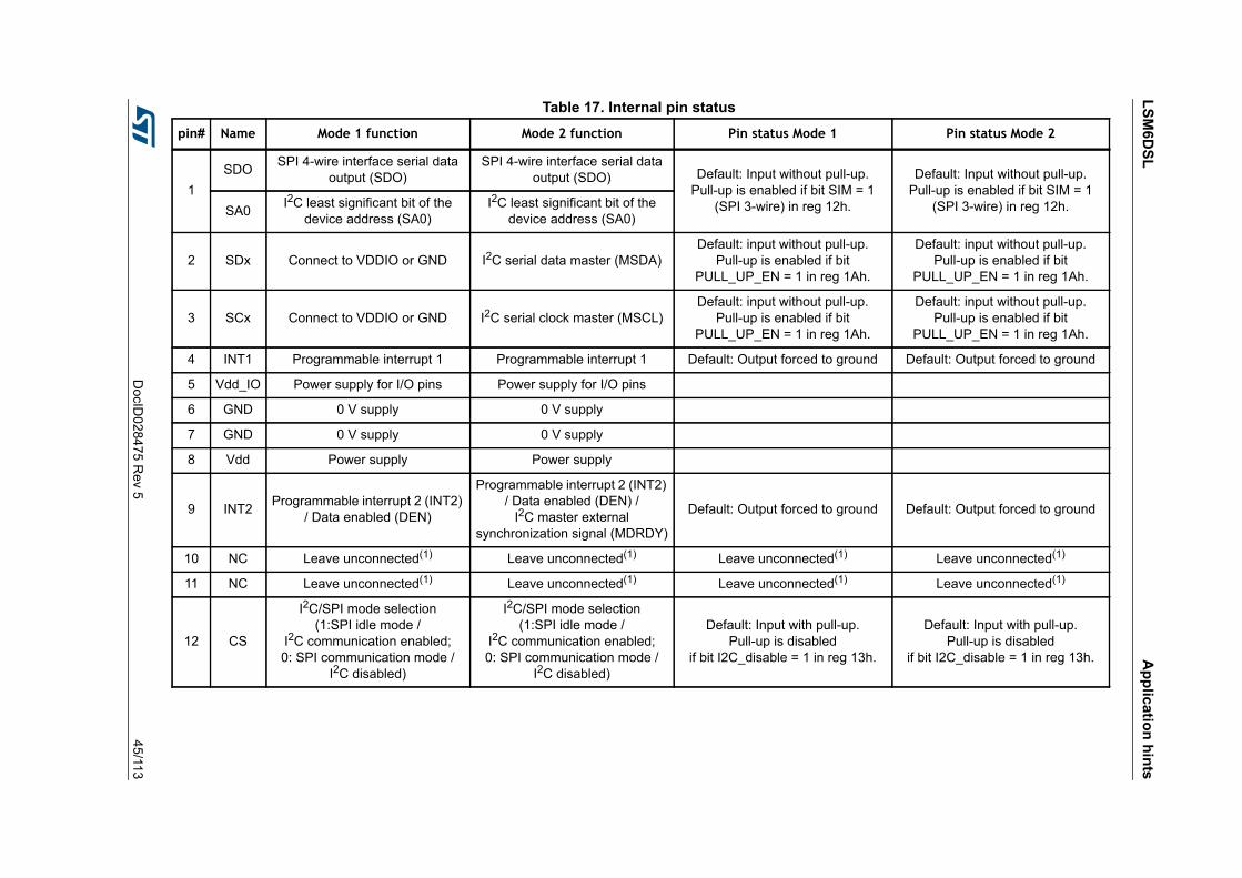
LSM6D
SLA
pplication hints
DocID
028475 Rev 5
45/113
Table 17. Internal pin status pin# Name Mode 1 function Mode 2 function Pin status Mode 1 Pin status Mode 2
1SDO SPI 4-wire interface serial data
output (SDO)SPI 4-wire interface serial data
output (SDO) Default: Input without pull-up. Pull-up is enabled if bit SIM = 1
(SPI 3-wire) in reg 12h.
Default: Input without pull-up. Pull-up is enabled if bit SIM = 1
(SPI 3-wire) in reg 12h.SA0 I2C least significant bit of the device address (SA0)
I2C least significant bit of the device address (SA0)
2 SDx Connect to VDDIO or GND I2C serial data master (MSDA)Default: input without pull-up.
Pull-up is enabled if bit PULL_UP_EN = 1 in reg 1Ah.
Default: input without pull-up. Pull-up is enabled if bit
PULL_UP_EN = 1 in reg 1Ah.
3 SCx Connect to VDDIO or GND I2C serial clock master (MSCL)Default: input without pull-up.
Pull-up is enabled if bit PULL_UP_EN = 1 in reg 1Ah.
Default: input without pull-up. Pull-up is enabled if bit
PULL_UP_EN = 1 in reg 1Ah.
4 INT1 Programmable interrupt 1 Programmable interrupt 1 Default: Output forced to ground Default: Output forced to ground
5 Vdd_IO Power supply for I/O pins Power supply for I/O pins
6 GND 0 V supply 0 V supply
7 GND 0 V supply 0 V supply
8 Vdd Power supply Power supply
9 INT2 Programmable interrupt 2 (INT2) / Data enabled (DEN)
Programmable interrupt 2 (INT2) / Data enabled (DEN) /
I2C master external synchronization signal (MDRDY)
Default: Output forced to ground Default: Output forced to ground
10 NC Leave unconnected(1) Leave unconnected(1) Leave unconnected(1) Leave unconnected(1)
11 NC Leave unconnected(1) Leave unconnected(1) Leave unconnected(1) Leave unconnected(1)
12 CS
I2C/SPI mode selection (1:SPI idle mode /
I2C communication enabled; 0: SPI communication mode /
I2C disabled)
I2C/SPI mode selection (1:SPI idle mode /
I2C communication enabled; 0: SPI communication mode /
I2C disabled)
Default: Input with pull-up. Pull-up is disabled
if bit I2C_disable = 1 in reg 13h.
Default: Input with pull-up. Pull-up is disabled
if bit I2C_disable = 1 in reg 13h.
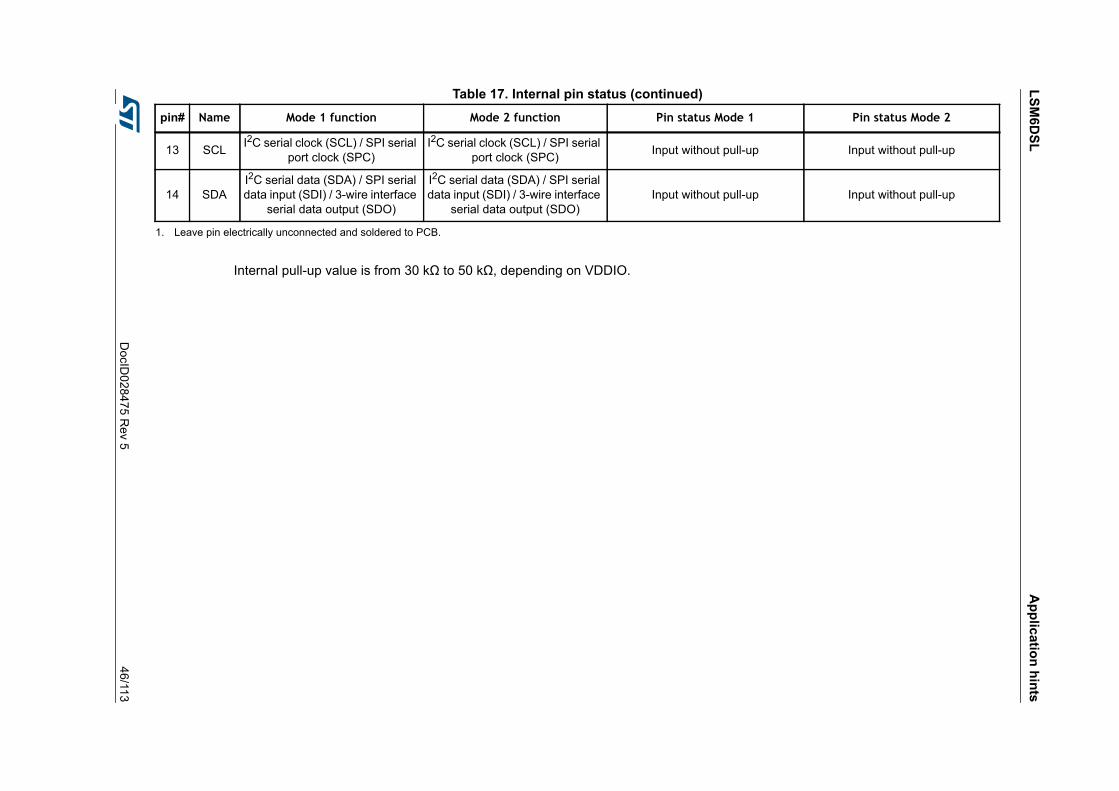
LSM6D
SLA
pplication hints
DocID
028475 Rev 5
46/113
Internal pull-up value is from 30 kΩ to 50 kΩ, depending on VDDIO.
13 SCL I2C serial clock (SCL) / SPI serial port clock (SPC)
I2C serial clock (SCL) / SPI serial port clock (SPC) Input without pull-up Input without pull-up
14 SDAI2C serial data (SDA) / SPI serial data input (SDI) / 3-wire interface
serial data output (SDO)
I2C serial data (SDA) / SPI serial data input (SDI) / 3-wire interface
serial data output (SDO)Input without pull-up Input without pull-up
1. Leave pin electrically unconnected and soldered to PCB.
Table 17. Internal pin status (continued)pin# Name Mode 1 function Mode 2 function Pin status Mode 1 Pin status Mode 2
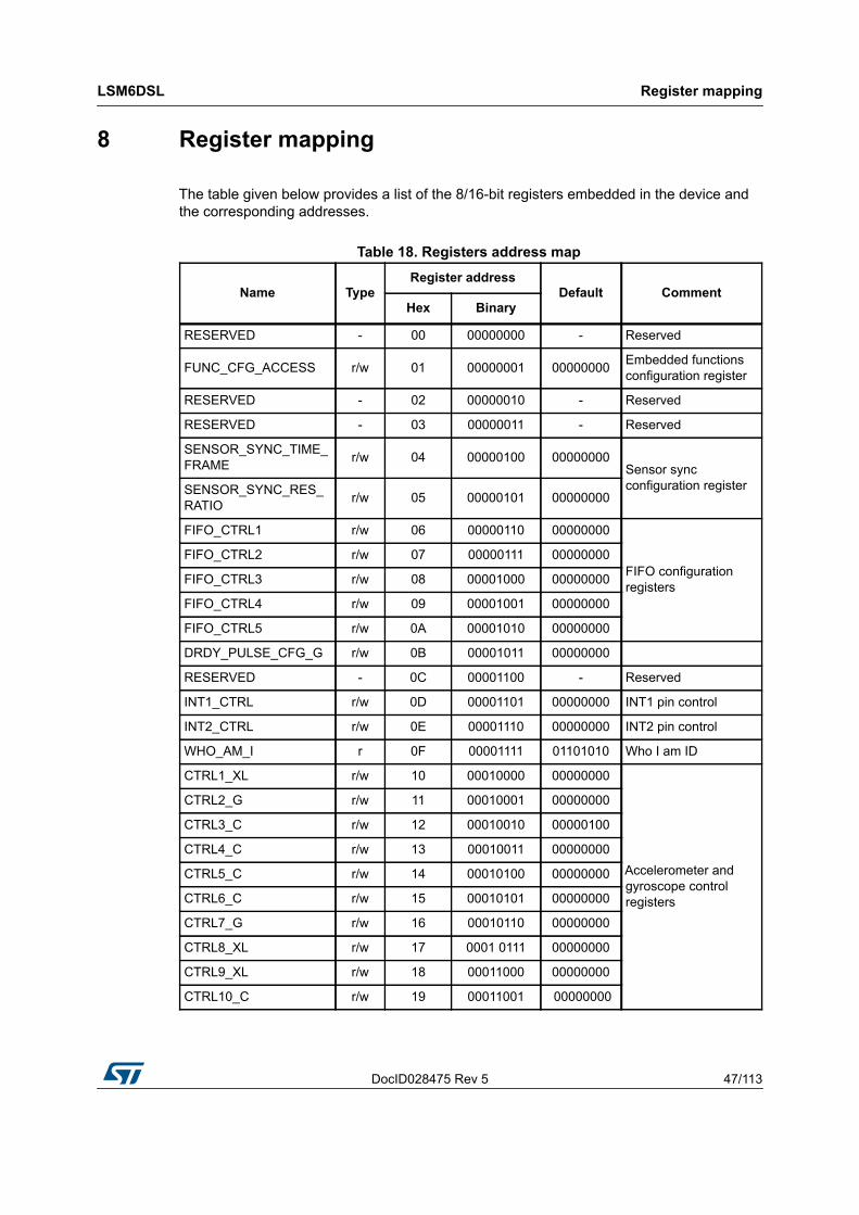
DocID028475 Rev 5 47/113
LSM6DSL Register mapping
113
8 Register mapping
The table given below provides a list of the 8/16-bit registers embedded in the device and the corresponding addresses.
Table 18. Registers address map
Name TypeRegister address
Default CommentHex Binary
RESERVED - 00 00000000 - Reserved
FUNC_CFG_ACCESS r/w 01 00000001 00000000 Embedded functions configuration register
RESERVED - 02 00000010 - Reserved
RESERVED - 03 00000011 - Reserved
SENSOR_SYNC_TIME_FRAME r/w 04 00000100 00000000
Sensor sync configuration registerSENSOR_SYNC_RES_
RATIO r/w 05 00000101 00000000
FIFO_CTRL1 r/w 06 00000110 00000000
FIFO configuration registers
FIFO_CTRL2 r/w 07 00000111 00000000
FIFO_CTRL3 r/w 08 00001000 00000000
FIFO_CTRL4 r/w 09 00001001 00000000
FIFO_CTRL5 r/w 0A 00001010 00000000
DRDY_PULSE_CFG_G r/w 0B 00001011 00000000
RESERVED - 0C 00001100 - Reserved
INT1_CTRL r/w 0D 00001101 00000000 INT1 pin control
INT2_CTRL r/w 0E 00001110 00000000 INT2 pin control
WHO_AM_I r 0F 00001111 01101010 Who I am ID
CTRL1_XL r/w 10 00010000 00000000
Accelerometer and gyroscope control registers
CTRL2_G r/w 11 00010001 00000000
CTRL3_C r/w 12 00010010 00000100
CTRL4_C r/w 13 00010011 00000000
CTRL5_C r/w 14 00010100 00000000
CTRL6_C r/w 15 00010101 00000000
CTRL7_G r/w 16 00010110 00000000
CTRL8_XL r/w 17 0001 0111 00000000
CTRL9_XL r/w 18 00011000 00000000
CTRL10_C r/w 19 00011001 00000000

Register mapping LSM6DSL
48/113 DocID028475 Rev 5
MASTER_CONFIG r/w 1A 00011010 00000000 I2C master configuration register
WAKE_UP_SRC r 1B 00011011 output
Interrupt registersTAP_SRC r 1C 00011100 output
D6D_SRC r 1D 00011101 output
STATUS_REG r 1E 00011110 output Status data register for user interface
RESERVED - 1F 00011111 -
OUT_TEMP_L r 20 00100000 output Temperature output data registersOUT_TEMP_H r 21 00100001 output
OUTX_L_G r 22 00100010 output
Gyroscope output registers for user interface
OUTX_H_G r 23 00100011 output
OUTY_L_G r 24 00100100 output
OUTY_H_G r 25 00100101 output
OUTZ_L_G r 26 00100110 output
OUTZ_H_G r 27 00100111 output
OUTX_L_XL r 28 00101000 output
Accelerometer output registers
OUTX_H_XL r 29 00101001 output
OUTY_L_XL r 2A 00101010 output
OUTY_H_XL r 2B 00101011 output
OUTZ_L_XL r 2C 00101100 output
OUTZ_H_XL r 2D 00101101 output
SENSORHUB1_REG r 2E 00101110 output
Sensor hub output registers
SENSORHUB2_REG r 2F 00101111 output
SENSORHUB3_REG r 30 00110000 output
SENSORHUB4_REG r 31 00110001 output
SENSORHUB5_REG r 32 00110010 output
SENSORHUB6_REG r 33 00110011 output
SENSORHUB7_REG r 34 00110100 output
SENSORHUB8_REG r 35 00110101 output
SENSORHUB9_REG r 36 00110110 output
SENSORHUB10_REG r 37 00110111 output
SENSORHUB11_REG r 38 00111000 output
SENSORHUB12_REG r 39 00111001 output
Table 18. Registers address map (continued)
Name TypeRegister address
Default CommentHex Binary

DocID028475 Rev 5 49/113
LSM6DSL Register mapping
113
FIFO_STATUS1 r 3A 00111010 output
FIFO status registersFIFO_STATUS2 r 3B 00111011 output
FIFO_STATUS3 r 3C 00111100 output
FIFO_STATUS4 r 3D 00111101 output
FIFO_DATA_OUT_L r 3E 00111110 output FIFO data output registersFIFO_DATA_OUT_H r 3F 00111111 output
TIMESTAMP0_REG r 40 01000000 outputTimestamp output registersTIMESTAMP1_REG r 41 01000001 output
TIMESTAMP2_REG r/w 42 01000010 output
RESERVED - 43-48 - Reserved
STEP_TIMESTAMP_L r 49 0100 1001 output Step counter timestamp registersSTEP_TIMESTAMP_H r 4A 0100 1010 output
STEP_COUNTER_L r 4B 01001011 output Step counter output registersSTEP_COUNTER_H r 4C 01001100 output
SENSORHUB13_REG r 4D 01001101 output
Sensor hub output registers
SENSORHUB14_REG r 4E 01001110 output
SENSORHUB15_REG r 4F 01001111 output
SENSORHUB16_REG r 50 01010000 output
SENSORHUB17_REG r 51 01010001 output
SENSORHUB18_REG r 52 01010010 output
FUNC_SRC1 r 53 01010011 outputInterrupt registers
FUNC_SRC2 r 54 01010100 output
WRIST_TILT_IA r 55 01010101 output Interrupt register
RESERVED - 56-57 - Reserved
TAP_CFG r/w 58 01011000 00000000
Interrupt registers
TAP_THS_6D r/w 59 01011001 00000000
INT_DUR2 r/w 5A 01011010 00000000
WAKE_UP_THS r/w 5B 01011011 00000000
WAKE_UP_DUR r/w 5C 01011100 00000000
FREE_FALL r/w 5D 01011101 00000000
MD1_CFG r/w 5E 01011110 00000000
MD2_CFG r/w 5F 01011111 00000000
MASTER_CMD_CODE r/w 60 01100000 00000000
Table 18. Registers address map (continued)
Name TypeRegister address
Default CommentHex Binary
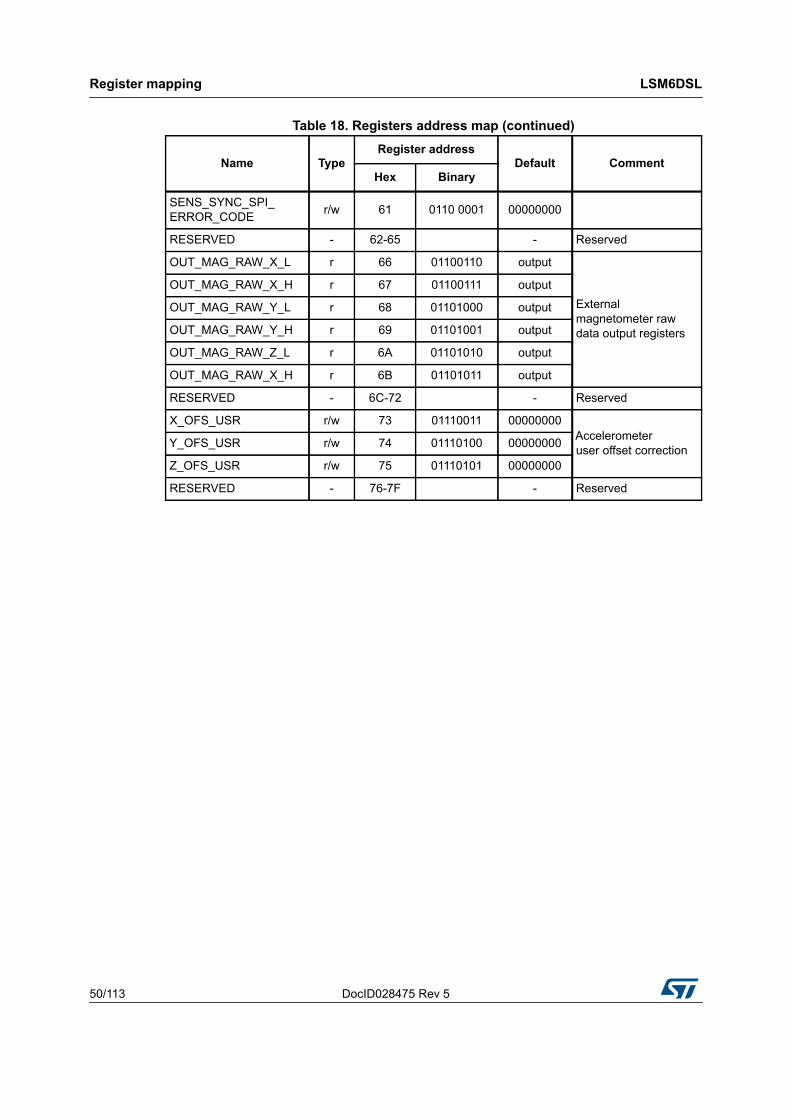
Register mapping LSM6DSL
50/113 DocID028475 Rev 5
SENS_SYNC_SPI_ERROR_CODE r/w 61 0110 0001 00000000
RESERVED - 62-65 - Reserved
OUT_MAG_RAW_X_L r 66 01100110 output
External magnetometer raw data output registers
OUT_MAG_RAW_X_H r 67 01100111 output
OUT_MAG_RAW_Y_L r 68 01101000 output
OUT_MAG_RAW_Y_H r 69 01101001 output
OUT_MAG_RAW_Z_L r 6A 01101010 output
OUT_MAG_RAW_X_H r 6B 01101011 output
RESERVED - 6C-72 - Reserved
X_OFS_USR r/w 73 01110011 00000000Accelerometeruser offset correctionY_OFS_USR r/w 74 01110100 00000000
Z_OFS_USR r/w 75 01110101 00000000
RESERVED - 76-7F - Reserved
Table 18. Registers address map (continued)
Name TypeRegister address
Default CommentHex Binary

DocID028475 Rev 5 51/113
LSM6DSL Register description
113
9 Register description
The device contains a set of registers which are used to control its behavior and to retrieve linear acceleration, angular rate and temperature data. The register addresses, made up of 7 bits, are used to identify them and to write the data through the serial interface.
9.1 FUNC_CFG_ACCESS (01h)Enable embedded functions register (r/w).
Table 20. FUNC_CFG_ACCESS register description
9.2 SENSOR_SYNC_TIME_FRAME (04h)Sensor synchronization time frame register (r/w).
Table 23. SENSOR_SYNC_TIME_FRAME register description
Table 19. FUNC_CFG_ACCESS registerFUNC_
CFG_EN 0(1)
1. This bit must be set to ‘0’ for the correct operation of the device.
FUNC_CFG_EN_B 0(1) 0(1) 0(1) 0(1) 0(1)
FUNC_CFG_EN
Enable access to the embedded functions configuration registers bank A and B(1). Default value: 0. Refer to Table 21.
1. The embedded functions configuration registers details are available in Section 10: Embedded functions register mapping, Section 11: Embedded functions registers description - Bank A, and Section 12: Embedded functions registers description - Bank B.
FUNC_CFG_EN_B
Enable access to the embedded functions configuration register bank B (1). Default value: 0. Refer to Table 21.
Table 21. Configuration of embedded functions register banksFUNC_CFG_EN FUNC_CFG_EN_B Status of embedded register banks
0 0 Bank A and B disabled (default)
0 1 Forbidden
1 0 Bank A enabled
1 1 Bank B enabled
Table 22. SENSOR_SYNC_TIME_FRAME register0(1)
1. This bit must be set to ‘0’ for the correct operation of the device.
0(1) 0(1) 0(1) TPH_3 TPH_2 TPH_1 TPH_0
TPH_ [3:0]Sensor synchronization time frame with the step of 500 ms and full range of 5 s. Unsigned 8-bit.Default value: 0000 0000 (sensor sync disabled)
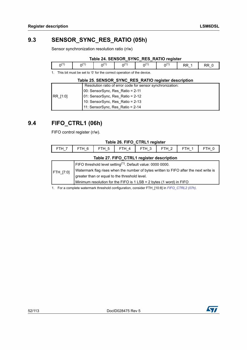
Register description LSM6DSL
52/113 DocID028475 Rev 5
9.3 SENSOR_SYNC_RES_RATIO (05h)Sensor synchronization resolution ratio (r/w)
Table 25. SENSOR_SYNC_RES_RATIO register description
9.4 FIFO_CTRL1 (06h)FIFO control register (r/w).
Table 27. FIFO_CTRL1 register description
Table 24. SENSOR_SYNC_RES_RATIO register0(1)
1. This bit must be set to ‘0’ for the correct operation of the device.
0(1) 0(1) 0(1) 0(1) 0(1) RR_1 RR_0
RR_[1:0]
Resolution ratio of error code for sensor synchronization:00: SensorSync, Res_Ratio = 2-1101: SensorSync, Res_Ratio = 2-1210: SensorSync, Res_Ratio = 2-1311: SensorSync, Res_Ratio = 2-14
Table 26. FIFO_CTRL1 registerFTH_7 FTH_6 FTH_5 FTH_4 FTH_3 FTH_2 FTH_1 FTH_0
FTH_[7:0]
FIFO threshold level setting(1). Default value: 0000 0000.Watermark flag rises when the number of bytes written to FIFO after the next write is greater than or equal to the threshold level.Minimum resolution for the FIFO is 1 LSB = 2 bytes (1 word) in FIFO
1. For a complete watermark threshold configuration, consider FTH_[10:8] in FIFO_CTRL2 (07h).
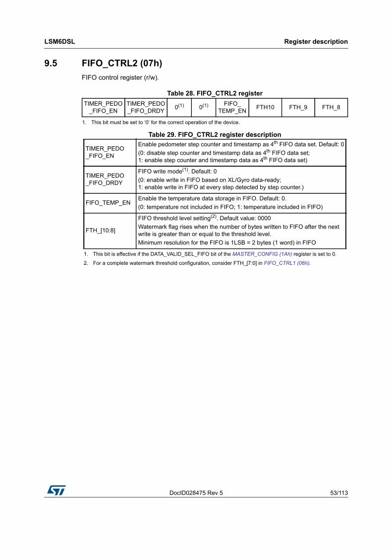
DocID028475 Rev 5 53/113
LSM6DSL Register description
113
9.5 FIFO_CTRL2 (07h)FIFO control register (r/w).
Table 29. FIFO_CTRL2 register description
Table 28. FIFO_CTRL2 registerTIMER_PEDO
_FIFO_ENTIMER_PEDO_FIFO_DRDY 0(1)
1. This bit must be set to ‘0’ for the correct operation of the device.
0(1) FIFO_TEMP_EN FTH10 FTH_9 FTH_8
TIMER_PEDO_FIFO_EN
Enable pedometer step counter and timestamp as 4th FIFO data set. Default: 0(0: disable step counter and timestamp data as 4th FIFO data set; 1: enable step counter and timestamp data as 4th FIFO data set)
TIMER_PEDO_FIFO_DRDY
FIFO write mode(1). Default: 0(0: enable write in FIFO based on XL/Gyro data-ready; 1: enable write in FIFO at every step detected by step counter.)
1. This bit is effective if the DATA_VALID_SEL_FIFO bit of the MASTER_CONFIG (1Ah) register is set to 0.
FIFO_TEMP_ENEnable the temperature data storage in FIFO. Default: 0.(0: temperature not included in FIFO; 1: temperature included in FIFO)
FTH_[10:8]
FIFO threshold level setting(2). Default value: 0000Watermark flag rises when the number of bytes written to FIFO after the next write is greater than or equal to the threshold level.Minimum resolution for the FIFO is 1LSB = 2 bytes (1 word) in FIFO
2. For a complete watermark threshold configuration, consider FTH_[7:0] in FIFO_CTRL1 (06h).
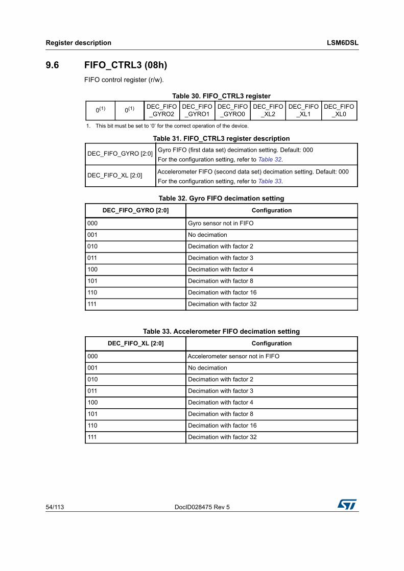
Register description LSM6DSL
54/113 DocID028475 Rev 5
9.6 FIFO_CTRL3 (08h)FIFO control register (r/w).
Table 31. FIFO_CTRL3 register description
Table 30. FIFO_CTRL3 register
0(1)
1. This bit must be set to ‘0’ for the correct operation of the device.
0(1) DEC_FIFO_GYRO2
DEC_FIFO_GYRO1
DEC_FIFO_GYRO0
DEC_FIFO_XL2
DEC_FIFO_XL1
DEC_FIFO_XL0
DEC_FIFO_GYRO [2:0] Gyro FIFO (first data set) decimation setting. Default: 000For the configuration setting, refer to Table 32.
DEC_FIFO_XL [2:0] Accelerometer FIFO (second data set) decimation setting. Default: 000For the configuration setting, refer to Table 33.
Table 32. Gyro FIFO decimation settingDEC_FIFO_GYRO [2:0] Configuration
000 Gyro sensor not in FIFO
001 No decimation
010 Decimation with factor 2
011 Decimation with factor 3
100 Decimation with factor 4
101 Decimation with factor 8
110 Decimation with factor 16
111 Decimation with factor 32
Table 33. Accelerometer FIFO decimation settingDEC_FIFO_XL [2:0] Configuration
000 Accelerometer sensor not in FIFO
001 No decimation
010 Decimation with factor 2
011 Decimation with factor 3
100 Decimation with factor 4
101 Decimation with factor 8
110 Decimation with factor 16
111 Decimation with factor 32
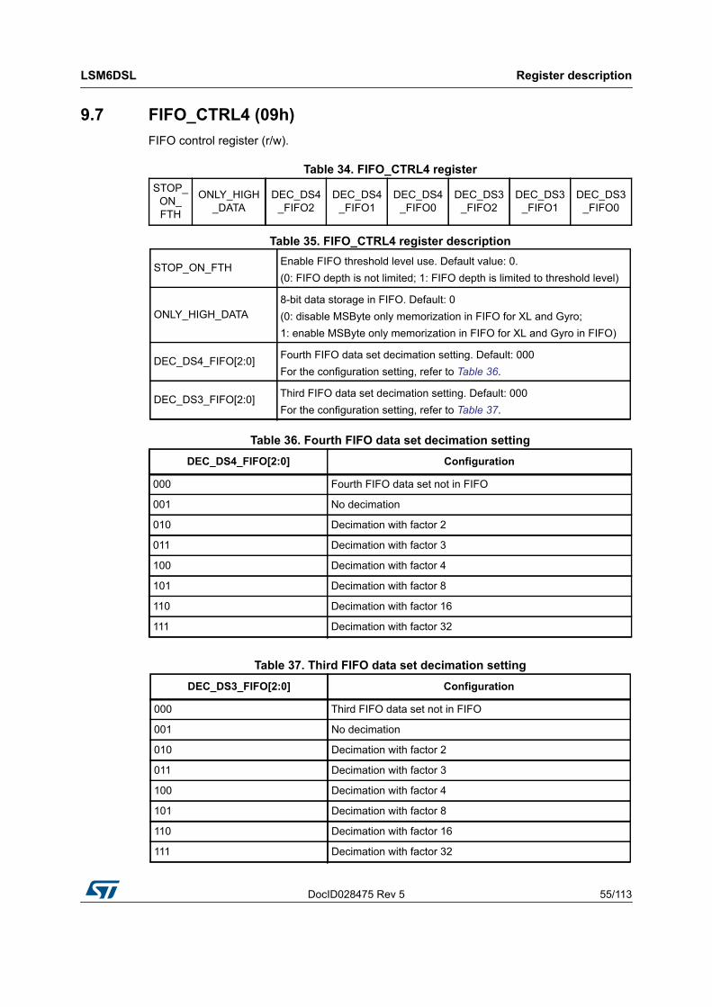
DocID028475 Rev 5 55/113
LSM6DSL Register description
113
9.7 FIFO_CTRL4 (09h)FIFO control register (r/w).
Table 35. FIFO_CTRL4 register description
Table 34. FIFO_CTRL4 registerSTOP_
ON_FTH
ONLY_HIGH_DATA
DEC_DS4_FIFO2
DEC_DS4_FIFO1
DEC_DS4_FIFO0
DEC_DS3_FIFO2
DEC_DS3_FIFO1
DEC_DS3_FIFO0
STOP_ON_FTH Enable FIFO threshold level use. Default value: 0.(0: FIFO depth is not limited; 1: FIFO depth is limited to threshold level)
ONLY_HIGH_DATA8-bit data storage in FIFO. Default: 0(0: disable MSByte only memorization in FIFO for XL and Gyro; 1: enable MSByte only memorization in FIFO for XL and Gyro in FIFO)
DEC_DS4_FIFO[2:0] Fourth FIFO data set decimation setting. Default: 000For the configuration setting, refer to Table 36.
DEC_DS3_FIFO[2:0] Third FIFO data set decimation setting. Default: 000For the configuration setting, refer to Table 37.
Table 36. Fourth FIFO data set decimation settingDEC_DS4_FIFO[2:0] Configuration
000 Fourth FIFO data set not in FIFO
001 No decimation
010 Decimation with factor 2
011 Decimation with factor 3
100 Decimation with factor 4
101 Decimation with factor 8
110 Decimation with factor 16
111 Decimation with factor 32
Table 37. Third FIFO data set decimation settingDEC_DS3_FIFO[2:0] Configuration
000 Third FIFO data set not in FIFO
001 No decimation
010 Decimation with factor 2
011 Decimation with factor 3
100 Decimation with factor 4
101 Decimation with factor 8
110 Decimation with factor 16
111 Decimation with factor 32

Register description LSM6DSL
56/113 DocID028475 Rev 5
9.8 FIFO_CTRL5 (0Ah)FIFO control register (r/w).
Table 39. FIFO_CTRL5 register description
Table 38. FIFO_CTRL5 register
0(1)
1. This bit must be set to ‘0’ for the correct operation of the device.
ODR_FIFO_3
ODR_FIFO_2
ODR_FIFO_1
ODR_FIFO_0
FIFO_MODE_2
FIFO_MODE_1
FIFO_MODE_0
ODR_FIFO_[3:0] FIFO ODR selection, setting FIFO_MODE also. Default: 0000For the configuration setting, refer to Table 40.
FIFO_MODE_[2:0]FIFO mode selection bits, setting ODR_FIFO also. Default value: 000 For the configuration setting, refer to Table 41.
Table 40. FIFO ODR selectionODR_FIFO_[3:0] Configuration(1)
1. If the device is working at an ODR slower than the one selected, FIFO ODR is limited to that ODR value. Moreover, these bits are effective if both the DATA_VALID_SEL_FIFO bit of MASTER_CONFIG (1Ah) and the TIMER_PEDO_FIFO_DRDY bit of FIFO_CTRL2 (07h) are set to 0.
0000 FIFO disabled
0001 FIFO ODR is set to 12.5 Hz
0010 FIFO ODR is set to 26 Hz
0011 FIFO ODR is set to 52 Hz
0100 FIFO ODR is set to 104 Hz
0101 FIFO ODR is set to 208 Hz
0110 FIFO ODR is set to 416 Hz
0111 FIFO ODR is set to 833 Hz
1000 FIFO ODR is set to 1.66 kHz
1001 FIFO ODR is set to 3.33 kHz
1010 FIFO ODR is set to 6.66 kHz
Table 41. FIFO mode selectionFIFO_MODE_[2:0] Configuration mode
000 Bypass mode. FIFO disabled.
001 FIFO mode. Stops collecting data when FIFO is full.
010 Reserved
011 Continuous mode until trigger is deasserted, then FIFO mode.
100 Bypass mode until trigger is deasserted, then Continuous mode.
101 Reserved
110 Continuous mode. If the FIFO is full, the new sample overwrites the older one.
111 Reserved
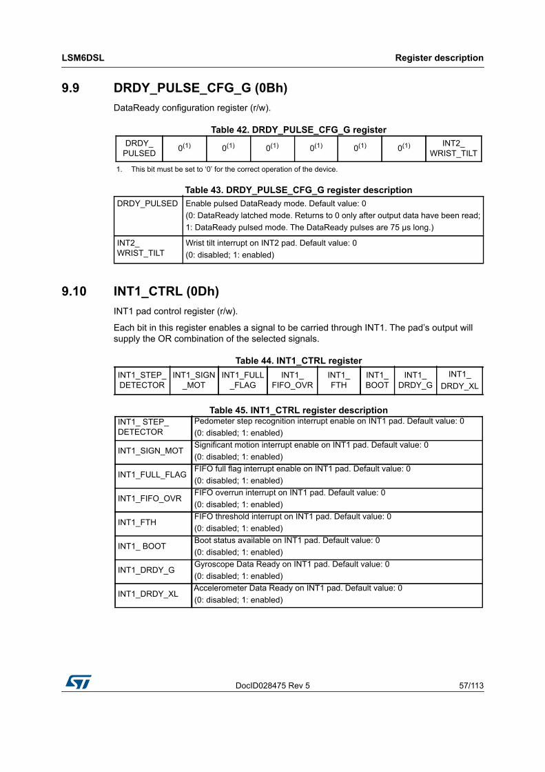
DocID028475 Rev 5 57/113
LSM6DSL Register description
113
9.9 DRDY_PULSE_CFG_G (0Bh)DataReady configuration register (r/w).
Table 42. DRDY_PULSE_CFG_G register
Table 43. DRDY_PULSE_CFG_G register description
9.10 INT1_CTRL (0Dh) INT1 pad control register (r/w).
Each bit in this register enables a signal to be carried through INT1. The pad’s output will supply the OR combination of the selected signals.
Table 44. INT1_CTRL register
Table 45. INT1_CTRL register description
DRDY_PULSED 0(1)
1. This bit must be set to ‘0’ for the correct operation of the device.
0(1) 0(1) 0(1) 0(1) 0(1) INT2_ WRIST_TILT
DRDY_PULSED Enable pulsed DataReady mode. Default value: 0(0: DataReady latched mode. Returns to 0 only after output data have been read;1: DataReady pulsed mode. The DataReady pulses are 75 μs long.)
INT2_WRIST_TILT
Wrist tilt interrupt on INT2 pad. Default value: 0(0: disabled; 1: enabled)
INT1_STEP_DETECTOR
INT1_SIGN_MOT
INT1_FULL_FLAG
INT1_FIFO_OVR
INT1_FTH
INT1_ BOOT
INT1_ DRDY_G
INT1_DRDY_XL
INT1_ STEP_DETECTOR
Pedometer step recognition interrupt enable on INT1 pad. Default value: 0(0: disabled; 1: enabled)
INT1_SIGN_MOTSignificant motion interrupt enable on INT1 pad. Default value: 0(0: disabled; 1: enabled)
INT1_FULL_FLAGFIFO full flag interrupt enable on INT1 pad. Default value: 0 (0: disabled; 1: enabled)
INT1_FIFO_OVRFIFO overrun interrupt on INT1 pad. Default value: 0(0: disabled; 1: enabled)
INT1_FTHFIFO threshold interrupt on INT1 pad. Default value: 0 (0: disabled; 1: enabled)
INT1_ BOOTBoot status available on INT1 pad. Default value: 0(0: disabled; 1: enabled)
INT1_DRDY_GGyroscope Data Ready on INT1 pad. Default value: 0 (0: disabled; 1: enabled)
INT1_DRDY_XLAccelerometer Data Ready on INT1 pad. Default value: 0 (0: disabled; 1: enabled)
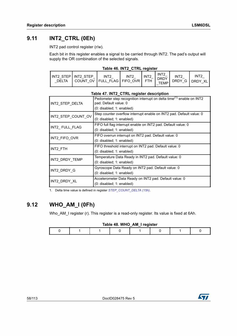
Register description LSM6DSL
58/113 DocID028475 Rev 5
9.11 INT2_CTRL (0Eh) INT2 pad control register (r/w).
Each bit in this register enables a signal to be carried through INT2. The pad’s output will supply the OR combination of the selected signals.
Table 46. INT2_CTRL register
Table 47. INT2_CTRL register description
9.12 WHO_AM_I (0Fh) Who_AM_I register (r). This register is a read-only register. Its value is fixed at 6Ah.
INT2_STEP_DELTA
INT2_STEP_COUNT_OV
INT2_ FULL_FLAG
INT2_FIFO_OVR
INT2_ FTH
INT2_DRDY_TEMP
INT2_ DRDY_G
INT2_DRDY_XL
INT2_STEP_DELTAPedometer step recognition interrupt on delta time(1) enable on INT2 pad. Default value: 0(0: disabled; 1: enabled)
1. Delta time value is defined in register STEP_COUNT_DELTA (15h).
INT2_STEP_COUNT_OVStep counter overflow interrupt enable on INT2 pad. Default value: 0(0: disabled; 1: enabled)
INT2_ FULL_FLAGFIFO full flag interrupt enable on INT2 pad. Default value: 0 (0: disabled; 1: enabled)
INT2_FIFO_OVRFIFO overrun interrupt on INT2 pad. Default value: 0 (0: disabled; 1: enabled)
INT2_FTHFIFO threshold interrupt on INT2 pad. Default value: 0 (0: disabled; 1: enabled)
INT2_DRDY_TEMPTemperature Data Ready in INT2 pad. Default value: 0(0: disabled; 1: enabled)
INT2_DRDY_GGyroscope Data Ready on INT2 pad. Default value: 0 (0: disabled; 1: enabled)
INT2_DRDY_XLAccelerometer Data Ready on INT2 pad. Default value: 0(0: disabled; 1: enabled)
Table 48. WHO_AM_I register0 1 1 0 1 0 1 0
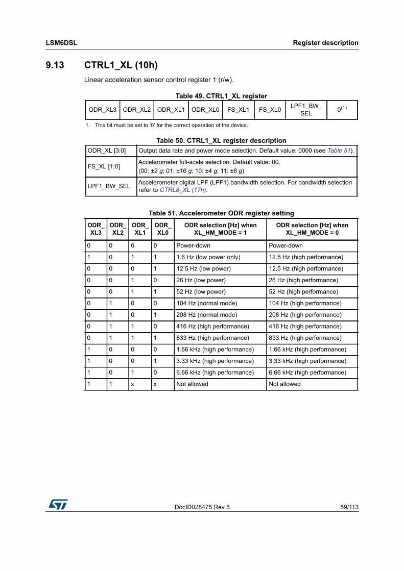
DocID028475 Rev 5 59/113
LSM6DSL Register description
113
9.13 CTRL1_XL (10h)Linear acceleration sensor control register 1 (r/w).
Table 49. CTRL1_XL register
Table 50. CTRL1_XL register description
ODR_XL3 ODR_XL2 ODR_XL1 ODR_XL0 FS_XL1 FS_XL0 LPF1_BW_SEL 0(1)
1. This bit must be set to ‘0’ for the correct operation of the device.
ODR_XL [3:0] Output data rate and power mode selection. Default value: 0000 (see Table 51).
FS_XL [1:0]Accelerometer full-scale selection. Default value: 00.(00: ±2 g; 01: ±16 g; 10: ±4 g; 11: ±8 g)
LPF1_BW_SEL Accelerometer digital LPF (LPF1) bandwidth selection. For bandwidth selection refer to CTRL8_XL (17h).
Table 51. Accelerometer ODR register setting ODR_XL3
ODR_XL2
ODR_XL1
ODR_XL0
ODR selection [Hz] when XL_HM_MODE = 1
ODR selection [Hz] when XL_HM_MODE = 0
0 0 0 0 Power-down Power-down
1 0 1 1 1.6 Hz (low power only) 12.5 Hz (high performance)
0 0 0 1 12.5 Hz (low power) 12.5 Hz (high performance)
0 0 1 0 26 Hz (low power) 26 Hz (high performance)
0 0 1 1 52 Hz (low power) 52 Hz (high performance)
0 1 0 0 104 Hz (normal mode) 104 Hz (high performance)
0 1 0 1 208 Hz (normal mode) 208 Hz (high performance)
0 1 1 0 416 Hz (high performance) 416 Hz (high performance)
0 1 1 1 833 Hz (high performance) 833 Hz (high performance)
1 0 0 0 1.66 kHz (high performance) 1.66 kHz (high performance)
1 0 0 1 3.33 kHz (high performance) 3.33 kHz (high performance)
1 0 1 0 6.66 kHz (high performance) 6.66 kHz (high performance)
1 1 x x Not allowed Not allowed
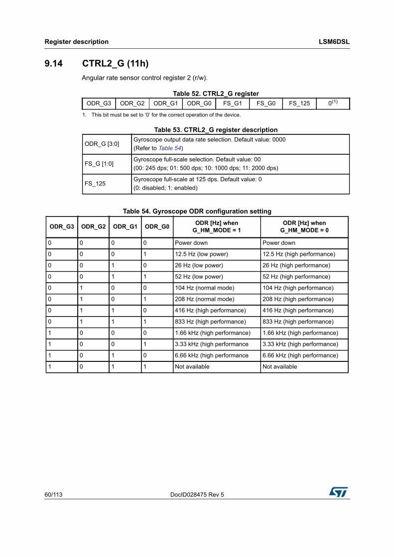
Register description LSM6DSL
60/113 DocID028475 Rev 5
9.14 CTRL2_G (11h)Angular rate sensor control register 2 (r/w).
Table 52. CTRL2_G register
Table 53. CTRL2_G register description
ODR_G3 ODR_G2 ODR_G1 ODR_G0 FS_G1 FS_G0 FS_125 0(1)
1. This bit must be set to ‘0’ for the correct operation of the device.
ODR_G [3:0]Gyroscope output data rate selection. Default value: 0000(Refer to Table 54)
FS_G [1:0]Gyroscope full-scale selection. Default value: 00(00: 245 dps; 01: 500 dps; 10: 1000 dps; 11: 2000 dps)
FS_125Gyroscope full-scale at 125 dps. Default value: 0(0: disabled; 1: enabled)
Table 54. Gyroscope ODR configuration setting
ODR_G3 ODR_G2 ODR_G1 ODR_G0 ODR [Hz] when G_HM_MODE = 1
ODR [Hz] when G_HM_MODE = 0
0 0 0 0 Power down Power down
0 0 0 1 12.5 Hz (low power) 12.5 Hz (high performance)
0 0 1 0 26 Hz (low power) 26 Hz (high performance)
0 0 1 1 52 Hz (low power) 52 Hz (high performance)
0 1 0 0 104 Hz (normal mode) 104 Hz (high performance)
0 1 0 1 208 Hz (normal mode) 208 Hz (high performance)
0 1 1 0 416 Hz (high performance) 416 Hz (high performance)
0 1 1 1 833 Hz (high performance) 833 Hz (high performance)
1 0 0 0 1.66 kHz (high performance) 1.66 kHz (high performance)
1 0 0 1 3.33 kHz (high performance 3.33 kHz (high performance)
1 0 1 0 6.66 kHz (high performance 6.66 kHz (high performance)
1 0 1 1 Not available Not available
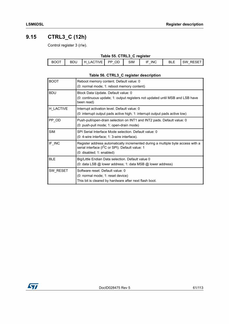
DocID028475 Rev 5 61/113
LSM6DSL Register description
113
9.15 CTRL3_C (12h)Control register 3 (r/w).
Table 55. CTRL3_C registerBOOT BDU H_LACTIVE PP_OD SIM IF_INC BLE SW_RESET
Table 56. CTRL3_C register description BOOT Reboot memory content. Default value: 0
(0: normal mode; 1: reboot memory content)
BDU Block Data Update. Default value: 0(0: continuous update; 1: output registers not updated until MSB and LSB have been read)
H_LACTIVE Interrupt activation level. Default value: 0(0: interrupt output pads active high; 1: interrupt output pads active low)
PP_OD Push-pull/open-drain selection on INT1 and INT2 pads. Default value: 0(0: push-pull mode; 1: open-drain mode)
SIM SPI Serial Interface Mode selection. Default value: 0 (0: 4-wire interface; 1: 3-wire interface).
IF_INC Register address automatically incremented during a multiple byte access with a serial interface (I2C or SPI). Default value: 1(0: disabled; 1: enabled)
BLE Big/Little Endian Data selection. Default value 0(0: data LSB @ lower address; 1: data MSB @ lower address)
SW_RESET Software reset. Default value: 0(0: normal mode; 1: reset device) This bit is cleared by hardware after next flash boot.
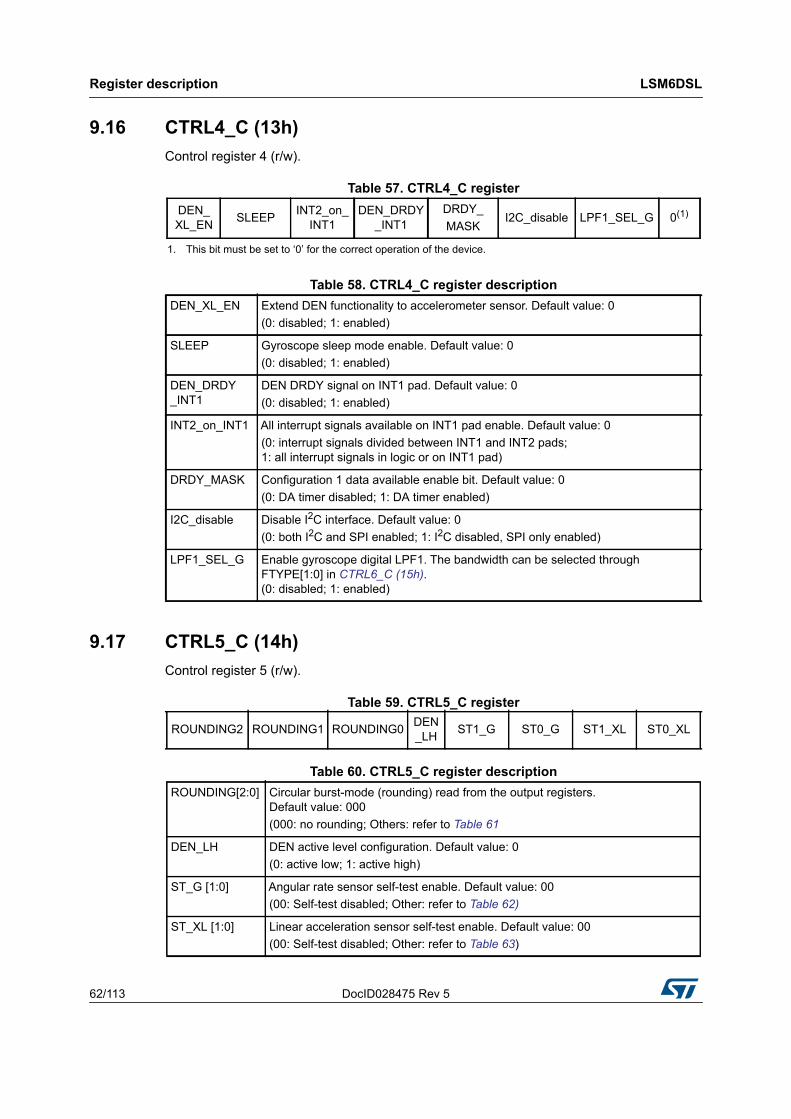
Register description LSM6DSL
62/113 DocID028475 Rev 5
9.16 CTRL4_C (13h)Control register 4 (r/w).
9.17 CTRL5_C (14h) Control register 5 (r/w).
Table 59. CTRL5_C register
Table 57. CTRL4_C registerDEN_XL_EN SLEEP INT2_on_
INT1DEN_DRDY
_INT1DRDY_MASK
I2C_disable LPF1_SEL_G 0(1)
1. This bit must be set to ‘0’ for the correct operation of the device.
Table 58. CTRL4_C register descriptionDEN_XL_EN Extend DEN functionality to accelerometer sensor. Default value: 0
(0: disabled; 1: enabled)
SLEEP Gyroscope sleep mode enable. Default value: 0(0: disabled; 1: enabled)
DEN_DRDY_INT1
DEN DRDY signal on INT1 pad. Default value: 0(0: disabled; 1: enabled)
INT2_on_INT1 All interrupt signals available on INT1 pad enable. Default value: 0(0: interrupt signals divided between INT1 and INT2 pads; 1: all interrupt signals in logic or on INT1 pad)
DRDY_MASK Configuration 1 data available enable bit. Default value: 0(0: DA timer disabled; 1: DA timer enabled)
I2C_disable Disable I2C interface. Default value: 0(0: both I2C and SPI enabled; 1: I2C disabled, SPI only enabled)
LPF1_SEL_G Enable gyroscope digital LPF1. The bandwidth can be selected through FTYPE[1:0] in CTRL6_C (15h).(0: disabled; 1: enabled)
ROUNDING2 ROUNDING1 ROUNDING0 DEN_LH ST1_G ST0_G ST1_XL ST0_XL
Table 60. CTRL5_C register descriptionROUNDING[2:0] Circular burst-mode (rounding) read from the output registers.
Default value: 000(000: no rounding; Others: refer to Table 61
DEN_LH DEN active level configuration. Default value: 0(0: active low; 1: active high)
ST_G [1:0] Angular rate sensor self-test enable. Default value: 00(00: Self-test disabled; Other: refer to Table 62)
ST_XL [1:0] Linear acceleration sensor self-test enable. Default value: 00(00: Self-test disabled; Other: refer to Table 63)
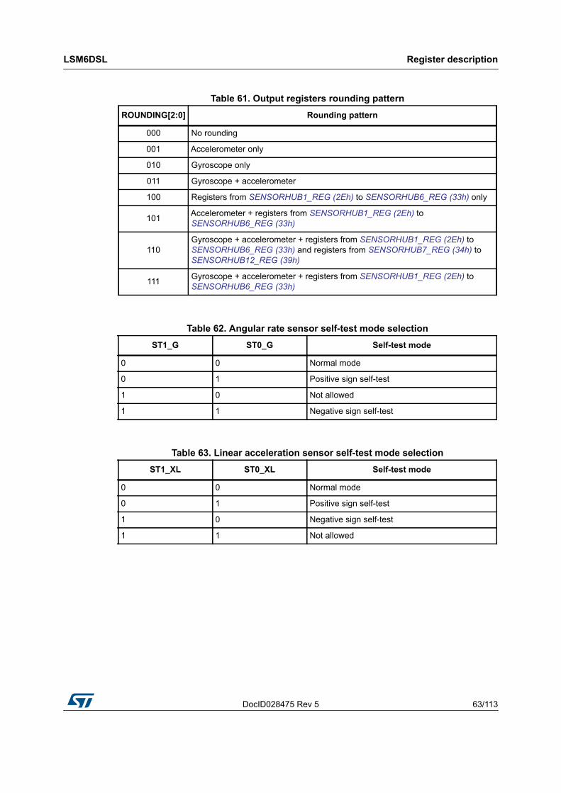
DocID028475 Rev 5 63/113
LSM6DSL Register description
113
Table 61. Output registers rounding patternROUNDING[2:0] Rounding pattern
000 No rounding
001 Accelerometer only
010 Gyroscope only
011 Gyroscope + accelerometer
100 Registers from SENSORHUB1_REG (2Eh) to SENSORHUB6_REG (33h) only
101 Accelerometer + registers from SENSORHUB1_REG (2Eh) to SENSORHUB6_REG (33h)
110Gyroscope + accelerometer + registers from SENSORHUB1_REG (2Eh) to SENSORHUB6_REG (33h) and registers from SENSORHUB7_REG (34h) to SENSORHUB12_REG (39h)
111 Gyroscope + accelerometer + registers from SENSORHUB1_REG (2Eh) to SENSORHUB6_REG (33h)
Table 62. Angular rate sensor self-test mode selectionST1_G ST0_G Self-test mode
0 0 Normal mode
0 1 Positive sign self-test
1 0 Not allowed
1 1 Negative sign self-test
Table 63. Linear acceleration sensor self-test mode selectionST1_XL ST0_XL Self-test mode
0 0 Normal mode
0 1 Positive sign self-test
1 0 Negative sign self-test
1 1 Not allowed
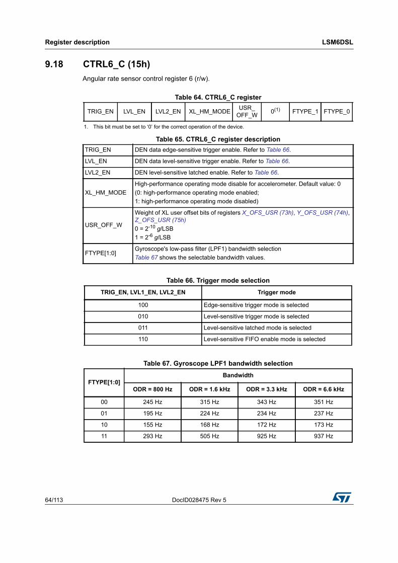
Register description LSM6DSL
64/113 DocID028475 Rev 5
9.18 CTRL6_C (15h)Angular rate sensor control register 6 (r/w).
Table 64. CTRL6_C register
TRIG_EN LVL_EN LVL2_EN XL_HM_MODE USR_OFF_W 0(1)
1. This bit must be set to ‘0’ for the correct operation of the device.
FTYPE_1 FTYPE_0
Table 65. CTRL6_C register descriptionTRIG_EN DEN data edge-sensitive trigger enable. Refer to Table 66.
LVL_EN DEN data level-sensitive trigger enable. Refer to Table 66.
LVL2_EN DEN level-sensitive latched enable. Refer to Table 66.
XL_HM_MODEHigh-performance operating mode disable for accelerometer. Default value: 0(0: high-performance operating mode enabled;1: high-performance operating mode disabled)
USR_OFF_W
Weight of XL user offset bits of registers X_OFS_USR (73h), Y_OFS_USR (74h), Z_OFS_USR (75h)0 = 2-10 g/LSB1 = 2-6 g/LSB
FTYPE[1:0]Gyroscope's low-pass filter (LPF1) bandwidth selection Table 67 shows the selectable bandwidth values.
Table 66. Trigger mode selectionTRIG_EN, LVL1_EN, LVL2_EN Trigger mode
100 Edge-sensitive trigger mode is selected
010 Level-sensitive trigger mode is selected
011 Level-sensitive latched mode is selected
110 Level-sensitive FIFO enable mode is selected
Table 67. Gyroscope LPF1 bandwidth selection
FTYPE[1:0]Bandwidth
ODR = 800 Hz ODR = 1.6 kHz ODR = 3.3 kHz ODR = 6.6 kHz
00 245 Hz 315 Hz 343 Hz 351 Hz
01 195 Hz 224 Hz 234 Hz 237 Hz
10 155 Hz 168 Hz 172 Hz 173 Hz
11 293 Hz 505 Hz 925 Hz 937 Hz

DocID028475 Rev 5 65/113
LSM6DSL Register description
113
9.19 CTRL7_G (16h)Angular rate sensor control register 7 (r/w).
9.20 CTRL8_XL (17h)Linear acceleration sensor control register 8 (r/w).
Table 68. CTRL7_G register
G_HM_MODE HP_EN_G HPM1_G HPM0_G 0(1)
1. This bit must be set to ‘0’ for the correct operation of the device.
ROUNDING_STATUS 0(1) 0(1)
Table 69. CTRL7_G register description
G_HM_MODEHigh-performance operating mode disable for gyroscope(1). Default: 0(0: high-performance operating mode enabled;1: high-performance operating mode disabled)
HP_EN_GGyroscope digital high-pass filter enable. The filter is enabled only if the gyro is in HP mode. Default value: 0(0: HPF disabled; 1: HPF enabled)
HPM_G[1:0]
Gyroscope digital HP filter cutoff selection. Default: 00(00 = 16 mHz01 = 65 mHz10 = 260 mHz11 = 1.04 Hz)
ROUNDING_STATUS
Source register rounding function on WAKE_UP_SRC (1Bh), TAP_SRC (1Ch), D6D_SRC (1Dh), STATUS_REG (1Eh), and FUNC_SRC (53h).Default value: 0(0: Rounding disabled; 1: Rounding enabled)
Table 70. CTRL8_XL register
LPF2_XL_EN
HPCF_XL1
HPCF_XL0
HP_REF_MODE
INPUT_COMPO
SITE
HP_SLOPE_XL_EN 0(1)
1. This bit must be set to ‘0’ for the correct operation of the device.
LOW_PASS_ON_6D
Table 71. CTRL8_XL register descriptionLPF2_XL_EN Accelerometer low-pass filter LPF2 selection. Refer to Figure 8.
HPCF_XL[1:0] Accelerometer LPF2 and high-pass filter configuration and cutoff setting. Refer to Table 72.
HP_REF_MODE Enable HP filter reference mode. Default value: 0(0: disabled; 1: enabled)
INPUT_COMPOSITEComposite filter input selection. Default: 0 (0: ODR/2 low pass filtered sent to composite filter (default)1: ODR/4 low pass filtered sent to composite filter)
HP_SLOPE_XL_EN Accelerometer slope filter / high-pass filter selection. Refer to Figure 8.
LOW_PASS_ON_6D LPF2 on 6D function selection. Refer to Figure 8.
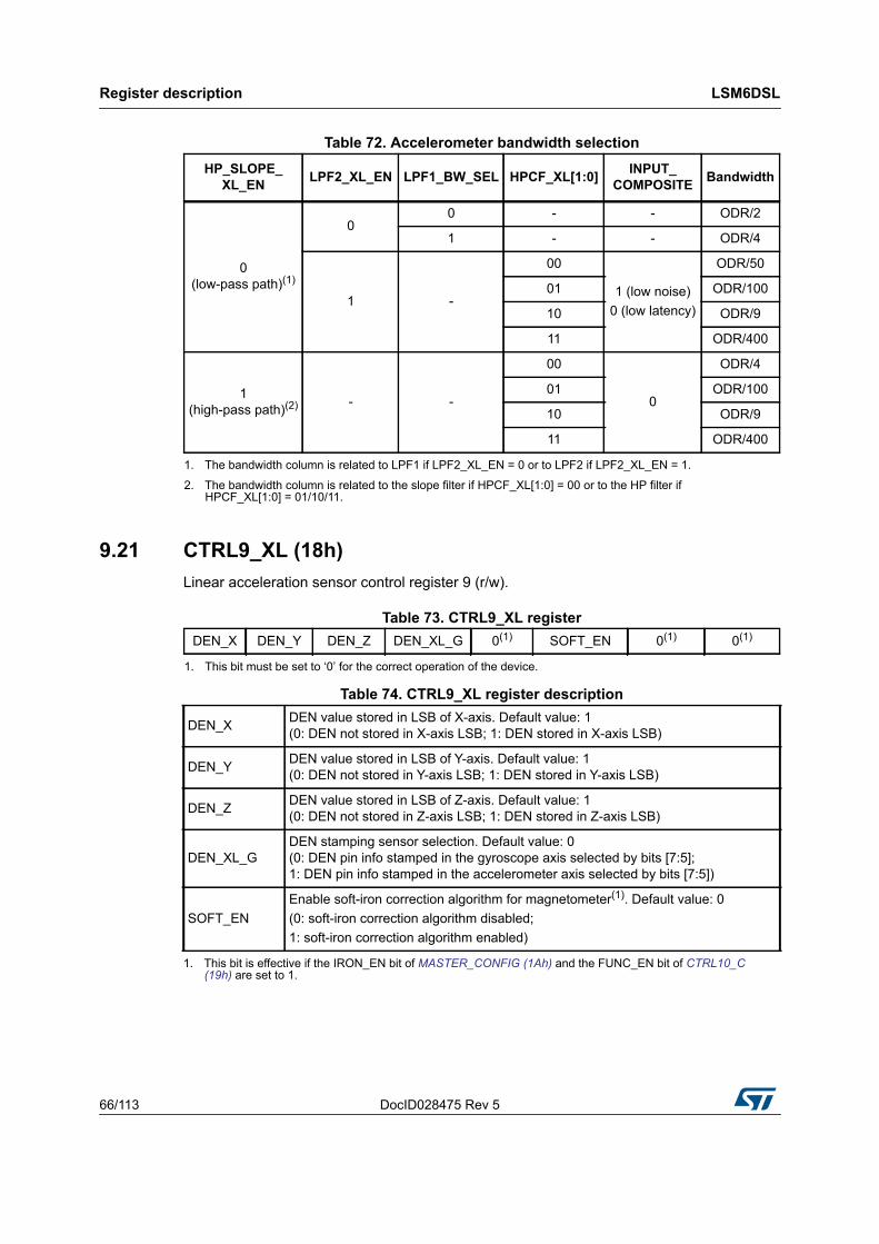
Register description LSM6DSL
66/113 DocID028475 Rev 5
9.21 CTRL9_XL (18h)Linear acceleration sensor control register 9 (r/w).
Table 72. Accelerometer bandwidth selectionHP_SLOPE_
XL_EN LPF2_XL_EN LPF1_BW_SEL HPCF_XL[1:0] INPUT_COMPOSITE Bandwidth
0 (low-pass path)(1)
1. The bandwidth column is related to LPF1 if LPF2_XL_EN = 0 or to LPF2 if LPF2_XL_EN = 1.
00 - - ODR/2
1 - - ODR/4
1 -
00
1 (low noise)0 (low latency)
ODR/50
01 ODR/100
10 ODR/9
11 ODR/400
1 (high-pass path)(2)
2. The bandwidth column is related to the slope filter if HPCF_XL[1:0] = 00 or to the HP filter if HPCF_XL[1:0] = 01/10/11.
- -
00
0
ODR/4
01 ODR/100
10 ODR/9
11 ODR/400
Table 73. CTRL9_XL registerDEN_X DEN_Y DEN_Z DEN_XL_G 0(1)
1. This bit must be set to ‘0’ for the correct operation of the device.
SOFT_EN 0(1) 0(1)
Table 74. CTRL9_XL register description
DEN_X DEN value stored in LSB of X-axis. Default value: 1 (0: DEN not stored in X-axis LSB; 1: DEN stored in X-axis LSB)
DEN_Y DEN value stored in LSB of Y-axis. Default value: 1 (0: DEN not stored in Y-axis LSB; 1: DEN stored in Y-axis LSB)
DEN_Z DEN value stored in LSB of Z-axis. Default value: 1 (0: DEN not stored in Z-axis LSB; 1: DEN stored in Z-axis LSB)
DEN_XL_GDEN stamping sensor selection. Default value: 0 (0: DEN pin info stamped in the gyroscope axis selected by bits [7:5]; 1: DEN pin info stamped in the accelerometer axis selected by bits [7:5])
SOFT_ENEnable soft-iron correction algorithm for magnetometer(1). Default value: 0(0: soft-iron correction algorithm disabled;1: soft-iron correction algorithm enabled)
1. This bit is effective if the IRON_EN bit of MASTER_CONFIG (1Ah) and the FUNC_EN bit of CTRL10_C (19h) are set to 1.
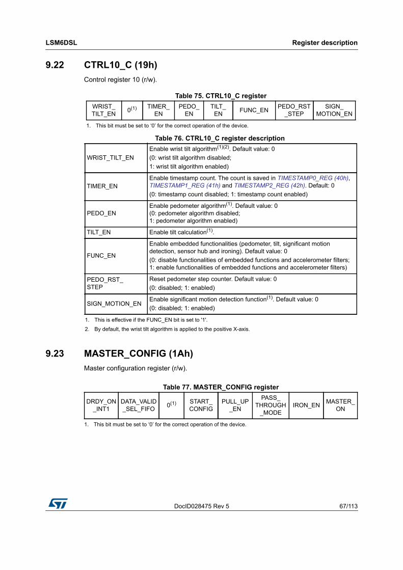
DocID028475 Rev 5 67/113
LSM6DSL Register description
113
9.22 CTRL10_C (19h)Control register 10 (r/w).
9.23 MASTER_CONFIG (1Ah)Master configuration register (r/w).
Table 75. CTRL10_C registerWRIST_TILT_EN 0(1)
1. This bit must be set to ‘0’ for the correct operation of the device.
TIMER_EN
PEDO_EN
TILT_EN FUNC_EN PEDO_RST
_STEPSIGN_
MOTION_EN
Table 76. CTRL10_C register description
WRIST_TILT_ENEnable wrist tilt algorithm(1)(2). Default value: 0(0: wrist tilt algorithm disabled;1: wrist tilt algorithm enabled)
1. This is effective if the FUNC_EN bit is set to '1'.
2. By default, the wrist tilt algorithm is applied to the positive X-axis.
TIMER_ENEnable timestamp count. The count is saved in TIMESTAMP0_REG (40h), TIMESTAMP1_REG (41h) and TIMESTAMP2_REG (42h). Default: 0(0: timestamp count disabled; 1: timestamp count enabled)
PEDO_ENEnable pedometer algorithm(1). Default value: 0(0: pedometer algorithm disabled;1: pedometer algorithm enabled)
TILT_EN Enable tilt calculation(1).
FUNC_EN
Enable embedded functionalities (pedometer, tilt, significant motion detection, sensor hub and ironing). Default value: 0(0: disable functionalities of embedded functions and accelerometer filters; 1: enable functionalities of embedded functions and accelerometer filters)
PEDO_RST_STEP
Reset pedometer step counter. Default value: 0(0: disabled; 1: enabled)
SIGN_MOTION_ENEnable significant motion detection function(1). Default value: 0(0: disabled; 1: enabled)
Table 77. MASTER_CONFIG register
DRDY_ON_INT1
DATA_VALID_SEL_FIFO 0(1)
1. This bit must be set to ‘0’ for the correct operation of the device.
START_CONFIG
PULL_UP_EN
PASS_THROUGH
_MODEIRON_EN MASTER_
ON
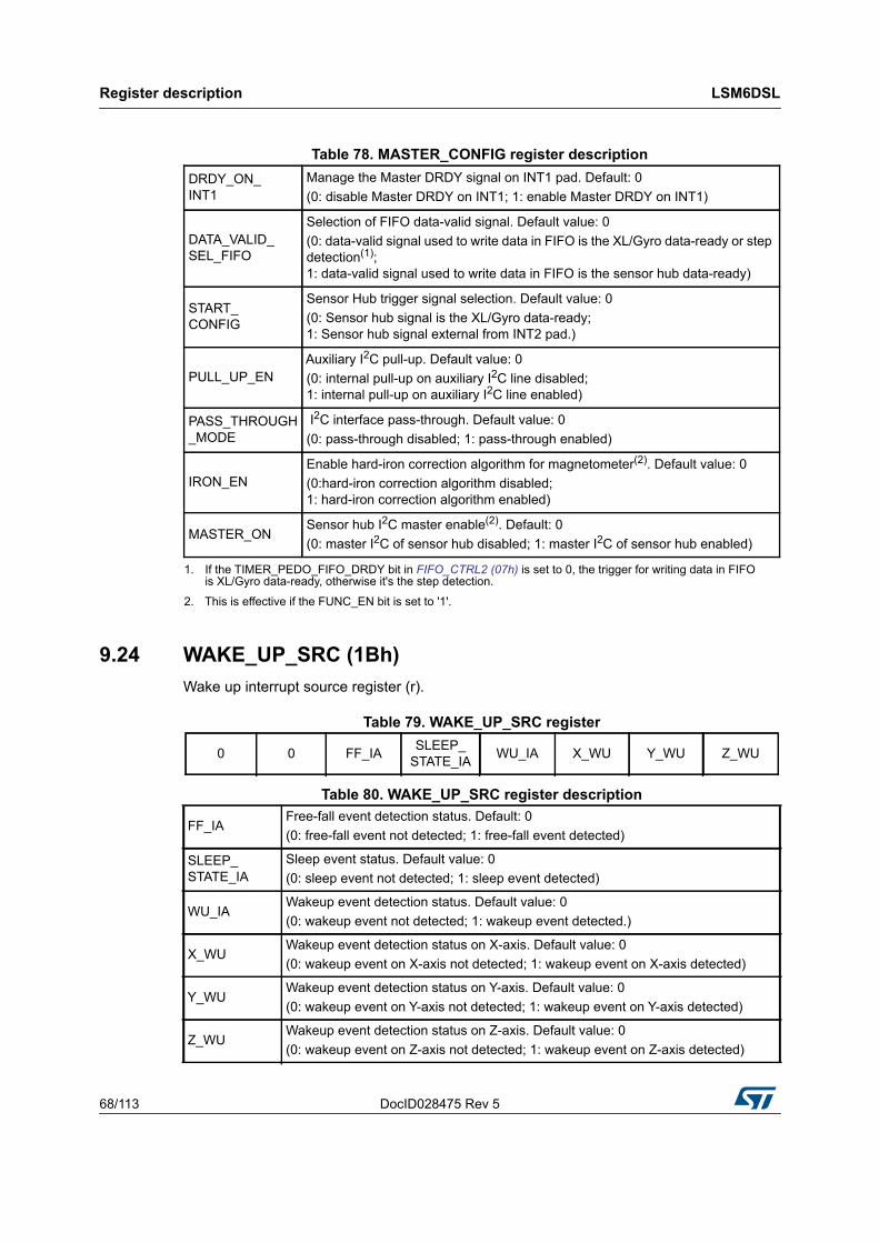
Register description LSM6DSL
68/113 DocID028475 Rev 5
9.24 WAKE_UP_SRC (1Bh)Wake up interrupt source register (r).
Table 78. MASTER_CONFIG register description DRDY_ON_INT1
Manage the Master DRDY signal on INT1 pad. Default: 0(0: disable Master DRDY on INT1; 1: enable Master DRDY on INT1)
DATA_VALID_SEL_FIFO
Selection of FIFO data-valid signal. Default value: 0(0: data-valid signal used to write data in FIFO is the XL/Gyro data-ready or step detection(1); 1: data-valid signal used to write data in FIFO is the sensor hub data-ready)
1. If the TIMER_PEDO_FIFO_DRDY bit in FIFO_CTRL2 (07h) is set to 0, the trigger for writing data in FIFO is XL/Gyro data-ready, otherwise it's the step detection.
START_CONFIG
Sensor Hub trigger signal selection. Default value: 0(0: Sensor hub signal is the XL/Gyro data-ready; 1: Sensor hub signal external from INT2 pad.)
PULL_UP_ENAuxiliary I2C pull-up. Default value: 0(0: internal pull-up on auxiliary I2C line disabled; 1: internal pull-up on auxiliary I2C line enabled)
PASS_THROUGH_MODE
I2C interface pass-through. Default value: 0(0: pass-through disabled; 1: pass-through enabled)
IRON_ENEnable hard-iron correction algorithm for magnetometer(2). Default value: 0(0:hard-iron correction algorithm disabled; 1: hard-iron correction algorithm enabled)
2. This is effective if the FUNC_EN bit is set to '1'.
MASTER_ONSensor hub I2C master enable(2). Default: 0(0: master I2C of sensor hub disabled; 1: master I2C of sensor hub enabled)
Table 79. WAKE_UP_SRC register
0 0 FF_IA SLEEP_STATE_IA WU_IA X_WU Y_WU Z_WU
Table 80. WAKE_UP_SRC register description
FF_IAFree-fall event detection status. Default: 0(0: free-fall event not detected; 1: free-fall event detected)
SLEEP_STATE_IA
Sleep event status. Default value: 0(0: sleep event not detected; 1: sleep event detected)
WU_IAWakeup event detection status. Default value: 0(0: wakeup event not detected; 1: wakeup event detected.)
X_WUWakeup event detection status on X-axis. Default value: 0(0: wakeup event on X-axis not detected; 1: wakeup event on X-axis detected)
Y_WUWakeup event detection status on Y-axis. Default value: 0(0: wakeup event on Y-axis not detected; 1: wakeup event on Y-axis detected)
Z_WUWakeup event detection status on Z-axis. Default value: 0(0: wakeup event on Z-axis not detected; 1: wakeup event on Z-axis detected)
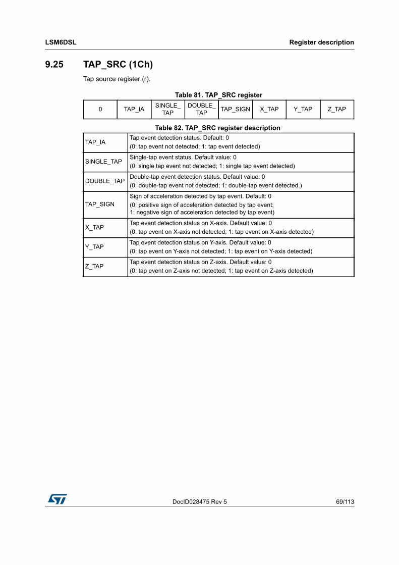
DocID028475 Rev 5 69/113
LSM6DSL Register description
113
9.25 TAP_SRC (1Ch)Tap source register (r).
Table 81. TAP_SRC register
0 TAP_IA SINGLE_TAP
DOUBLE_TAP TAP_SIGN X_TAP Y_TAP Z_TAP
Table 82. TAP_SRC register description
TAP_IATap event detection status. Default: 0(0: tap event not detected; 1: tap event detected)
SINGLE_TAPSingle-tap event status. Default value: 0(0: single tap event not detected; 1: single tap event detected)
DOUBLE_TAPDouble-tap event detection status. Default value: 0(0: double-tap event not detected; 1: double-tap event detected.)
TAP_SIGNSign of acceleration detected by tap event. Default: 0(0: positive sign of acceleration detected by tap event; 1: negative sign of acceleration detected by tap event)
X_TAPTap event detection status on X-axis. Default value: 0(0: tap event on X-axis not detected; 1: tap event on X-axis detected)
Y_TAPTap event detection status on Y-axis. Default value: 0(0: tap event on Y-axis not detected; 1: tap event on Y-axis detected)
Z_TAPTap event detection status on Z-axis. Default value: 0(0: tap event on Z-axis not detected; 1: tap event on Z-axis detected)
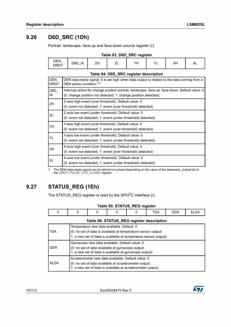
Register description LSM6DSL
70/113 DocID028475 Rev 5
9.26 D6D_SRC (1Dh)Portrait, landscape, face-up and face-down source register (r)
9.27 STATUS_REG (1Eh)The STATUS_REG register is read by the SPI/I2C interface (r).
Table 83. D6D_SRC registerDEN_DRDY D6D_IA ZH ZL YH YL XH XL
Table 84. D6D_SRC register descriptionDEN_DRDY
DEN data-ready signal. It is set high when data output is related to the data coming from a DEN active condition.(1)
1. The DEN data-ready signal can be latched or pulsed depending on the value of the dataready_pulsed bit of the DRDY_PULSE_CFG_G (0Bh) register.
D6D_IA
Interrupt active for change position portrait, landscape, face-up, face-down. Default value: 0(0: change position not detected; 1: change position detected)
ZHZ-axis high event (over threshold). Default value: 0(0: event not detected; 1: event (over threshold) detected)
ZLZ-axis low event (under threshold). Default value: 0(0: event not detected; 1: event (under threshold) detected)
YHY-axis high event (over threshold). Default value: 0(0: event not detected; 1: event (over-threshold) detected)
YLY-axis low event (under threshold). Default value: 0(0: event not detected; 1: event (under threshold) detected)
XHX-axis high event (over threshold). Default value: 0(0: event not detected; 1: event (over threshold) detected)
XLX-axis low event (under threshold). Default value: 0(0: event not detected; 1: event (under threshold) detected)
Table 85. STATUS_REG register0 0 0 0 0 TDA GDA XLDA
Table 86. STATUS_REG register description
TDATemperature new data available. Default: 0(0: no set of data is available at temperature sensor output;1: a new set of data is available at temperature sensor output)
GDAGyroscope new data available. Default value: 0(0: no set of data available at gyroscope output; 1: a new set of data is available at gyroscope output)
XLDAAccelerometer new data available. Default value: 0(0: no set of data available at accelerometer output; 1: a new set of data is available at accelerometer output)
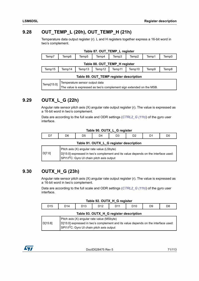
DocID028475 Rev 5 71/113
LSM6DSL Register description
113
9.28 OUT_TEMP_L (20h), OUT_TEMP_H (21h)Temperature data output register (r). L and H registers together express a 16-bit word in two’s complement.
9.29 OUTX_L_G (22h)Angular rate sensor pitch axis (X) angular rate output register (r). The value is expressed as a 16-bit word in two’s complement.
Data are according to the full scale and ODR settings (CTRL2_G (11h)) of the gyro user interface.
9.30 OUTX_H_G (23h)Angular rate sensor pitch axis (X) angular rate output register (r). The value is expressed as a 16-bit word in two’s complement.
Data are according to the full scale and ODR settings (CTRL2_G (11h)) of the gyro user interface.
Table 87. OUT_TEMP_L registerTemp7 Temp6 Temp5 Temp4 Temp3 Temp2 Temp1 Temp0
Table 88. OUT_TEMP_H registerTemp15 Temp14 Temp13 Temp12 Temp11 Temp10 Temp9 Temp8
Table 89. OUT_TEMP register description
Temp[15:0] Temperature sensor output dataThe value is expressed as two’s complement sign extended on the MSB.
Table 90. OUTX_L_G registerD7 D6 D5 D4 D3 D2 D1 D0
Table 91. OUTX_L_G register description
D[7:0]Pitch axis (X) angular rate value (LSbyte)D[15:0] expressed in two’s complement and its value depends on the interface used:SPI1/I2C: Gyro UI chain pitch axis output
Table 92. OUTX_H_G registerD15 D14 D13 D12 D11 D10 D9 D8
Table 93. OUTX_H_G register description
D[15:8]Pitch axis (X) angular rate value (MSbyte)D[15:0] expressed in two’s complement and its value depends on the interface used:SPI1/I2C: Gyro UI chain pitch axis output
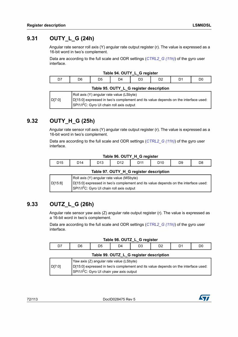
Register description LSM6DSL
72/113 DocID028475 Rev 5
9.31 OUTY_L_G (24h)Angular rate sensor roll axis (Y) angular rate output register (r). The value is expressed as a 16-bit word in two’s complement.
Data are according to the full scale and ODR settings (CTRL2_G (11h)) of the gyro user interface.
9.32 OUTY_H_G (25h)Angular rate sensor roll axis (Y) angular rate output register (r). The value is expressed as a 16-bit word in two’s complement.
Data are according to the full scale and ODR settings (CTRL2_G (11h)) of the gyro user interface.
9.33 OUTZ_L_G (26h)Angular rate sensor yaw axis (Z) angular rate output register (r). The value is expressed as a 16-bit word in two’s complement.
Data are according to the full scale and ODR settings (CTRL2_G (11h)) of the gyro user interface.
Table 94. OUTY_L_G registerD7 D6 D5 D4 D3 D2 D1 D0
Table 95. OUTY_L_G register description
D[7:0]Roll axis (Y) angular rate value (LSbyte)D[15:0] expressed in two’s complement and its value depends on the interface used:SPI1/I2C: Gyro UI chain roll axis output
Table 96. OUTY_H_G registerD15 D14 D13 D12 D11 D10 D9 D8
Table 97. OUTY_H_G register description
D[15:8]Roll axis (Y) angular rate value (MSbyte)D[15:0] expressed in two’s complement and its value depends on the interface used:SPI1/I2C: Gyro UI chain roll axis output
Table 98. OUTZ_L_G registerD7 D6 D5 D4 D3 D2 D1 D0
Table 99. OUTZ_L_G register description
D[7:0]Yaw axis (Z) angular rate value (LSbyte)D[15:0] expressed in two’s complement and its value depends on the interface used:SPI1/I2C: Gyro UI chain yaw axis output
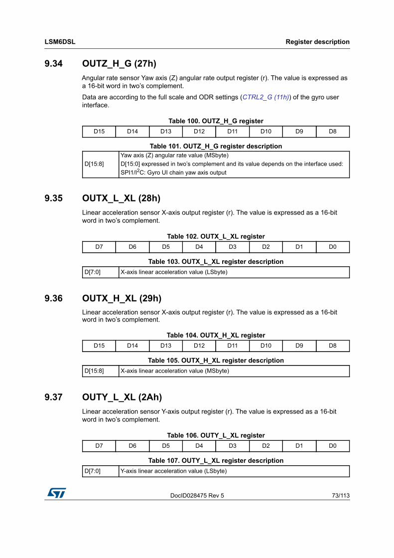
DocID028475 Rev 5 73/113
LSM6DSL Register description
113
9.34 OUTZ_H_G (27h)Angular rate sensor Yaw axis (Z) angular rate output register (r). The value is expressed as a 16-bit word in two’s complement.
Data are according to the full scale and ODR settings (CTRL2_G (11h)) of the gyro user interface.
9.35 OUTX_L_XL (28h)Linear acceleration sensor X-axis output register (r). The value is expressed as a 16-bit word in two’s complement.
9.36 OUTX_H_XL (29h)Linear acceleration sensor X-axis output register (r). The value is expressed as a 16-bit word in two’s complement.
9.37 OUTY_L_XL (2Ah)Linear acceleration sensor Y-axis output register (r). The value is expressed as a 16-bit word in two’s complement.
Table 100. OUTZ_H_G registerD15 D14 D13 D12 D11 D10 D9 D8
Table 101. OUTZ_H_G register description
D[15:8]Yaw axis (Z) angular rate value (MSbyte)D[15:0] expressed in two’s complement and its value depends on the interface used:SPI1/I2C: Gyro UI chain yaw axis output
Table 102. OUTX_L_XL registerD7 D6 D5 D4 D3 D2 D1 D0
Table 103. OUTX_L_XL register descriptionD[7:0] X-axis linear acceleration value (LSbyte)
Table 104. OUTX_H_XL registerD15 D14 D13 D12 D11 D10 D9 D8
Table 105. OUTX_H_XL register descriptionD[15:8] X-axis linear acceleration value (MSbyte)
Table 106. OUTY_L_XL registerD7 D6 D5 D4 D3 D2 D1 D0
Table 107. OUTY_L_XL register descriptionD[7:0] Y-axis linear acceleration value (LSbyte)
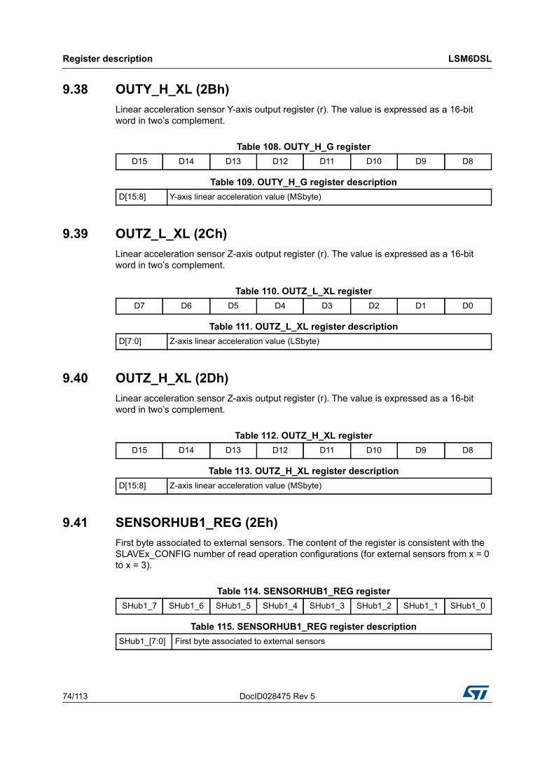
Register description LSM6DSL
74/113 DocID028475 Rev 5
9.38 OUTY_H_XL (2Bh)Linear acceleration sensor Y-axis output register (r). The value is expressed as a 16-bit word in two’s complement.
9.39 OUTZ_L_XL (2Ch)Linear acceleration sensor Z-axis output register (r). The value is expressed as a 16-bit word in two’s complement.
9.40 OUTZ_H_XL (2Dh)Linear acceleration sensor Z-axis output register (r). The value is expressed as a 16-bit word in two’s complement.
9.41 SENSORHUB1_REG (2Eh)First byte associated to external sensors. The content of the register is consistent with the SLAVEx_CONFIG number of read operation configurations (for external sensors from x = 0 to x = 3).
Table 108. OUTY_H_G registerD15 D14 D13 D12 D11 D10 D9 D8
Table 109. OUTY_H_G register descriptionD[15:8] Y-axis linear acceleration value (MSbyte)
Table 110. OUTZ_L_XL registerD7 D6 D5 D4 D3 D2 D1 D0
Table 111. OUTZ_L_XL register descriptionD[7:0] Z-axis linear acceleration value (LSbyte)
Table 112. OUTZ_H_XL registerD15 D14 D13 D12 D11 D10 D9 D8
Table 113. OUTZ_H_XL register descriptionD[15:8] Z-axis linear acceleration value (MSbyte)
Table 114. SENSORHUB1_REG registerSHub1_7 SHub1_6 SHub1_5 SHub1_4 SHub1_3 SHub1_2 SHub1_1 SHub1_0
Table 115. SENSORHUB1_REG register descriptionSHub1_[7:0] First byte associated to external sensors
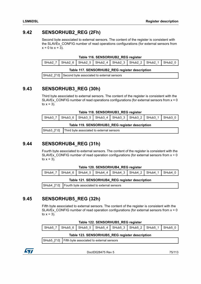
DocID028475 Rev 5 75/113
LSM6DSL Register description
113
9.42 SENSORHUB2_REG (2Fh)Second byte associated to external sensors. The content of the register is consistent with the SLAVEx_CONFIG number of read operations configurations (for external sensors from x = 0 to x = 3).
9.43 SENSORHUB3_REG (30h)Third byte associated to external sensors. The content of the register is consistent with the SLAVEx_CONFIG number of read operations configurations (for external sensors from x = 0 to x = 3).
9.44 SENSORHUB4_REG (31h)Fourth byte associated to external sensors. The content of the register is consistent with the SLAVEx_CONFIG number of read operation configurations (for external sensors from x = 0 to x = 3).
9.45 SENSORHUB5_REG (32h)Fifth byte associated to external sensors. The content of the register is consistent with the SLAVEx_CONFIG number of read operation configurations (for external sensors from x = 0 to x = 3).
Table 116. SENSORHUB2_REG registerSHub2_7 SHub2_6 SHub2_5 SHub2_4 SHub2_3 SHub2_2 SHub2_1 SHub2_0
Table 117. SENSORHUB2_REG register descriptionSHub2_[7:0] Second byte associated to external sensors
Table 118. SENSORHUB3_REG registerSHub3_7 SHub3_6 SHub3_5 SHub3_4 SHub3_3 SHub3_2 SHub3_1 SHub3_0
Table 119. SENSORHUB3_REG register descriptionSHub3_[7:0] Third byte associated to external sensors
Table 120. SENSORHUB4_REG registerSHub4_7 SHub4_6 SHub4_5 SHub4_4 SHub4_3 SHub4_2 SHub4_1 SHub4_0
Table 121. SENSORHUB4_REG register descriptionSHub4_[7:0] Fourth byte associated to external sensors
Table 122. SENSORHUB5_REG registerSHub5_7 SHub5_6 SHub5_5 SHub5_4 SHub5_3 SHub5_2 SHub5_1 SHub5_0
Table 123. SENSORHUB5_REG register descriptionSHub5_[7:0] Fifth byte associated to external sensors
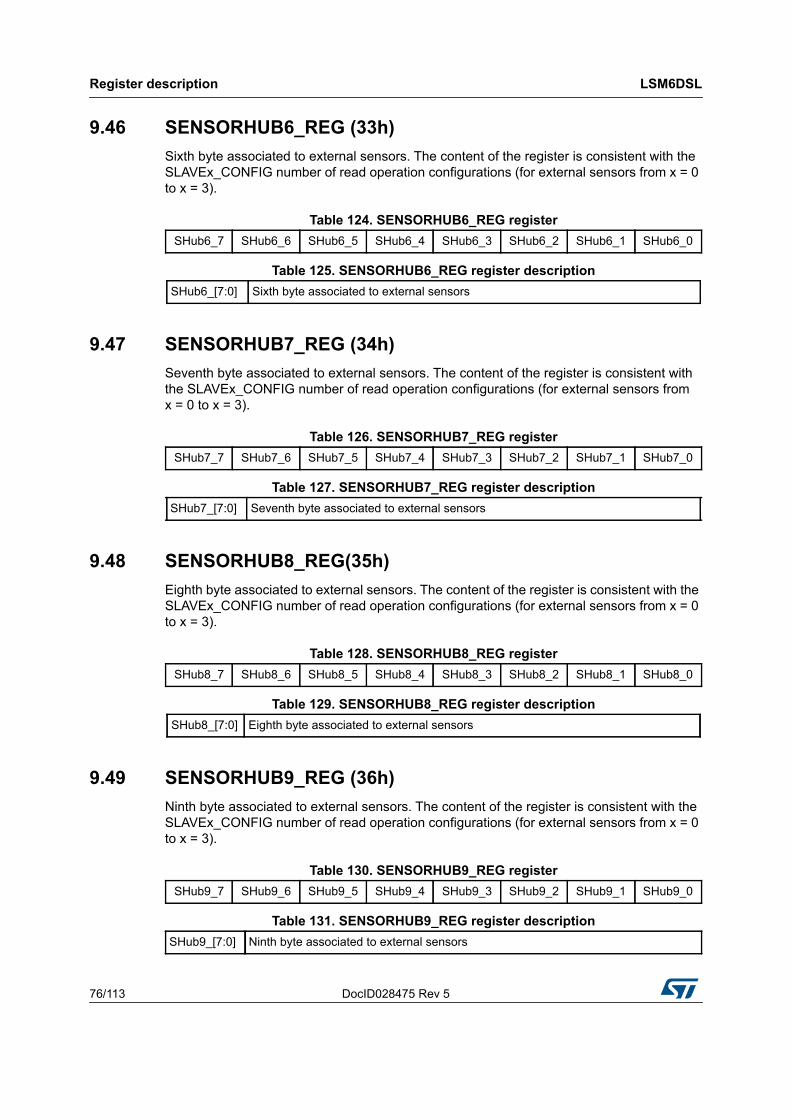
Register description LSM6DSL
76/113 DocID028475 Rev 5
9.46 SENSORHUB6_REG (33h)Sixth byte associated to external sensors. The content of the register is consistent with the SLAVEx_CONFIG number of read operation configurations (for external sensors from x = 0 to x = 3).
9.47 SENSORHUB7_REG (34h)Seventh byte associated to external sensors. The content of the register is consistent with the SLAVEx_CONFIG number of read operation configurations (for external sensors from x = 0 to x = 3).
9.48 SENSORHUB8_REG(35h)Eighth byte associated to external sensors. The content of the register is consistent with the SLAVEx_CONFIG number of read operation configurations (for external sensors from x = 0 to x = 3).
9.49 SENSORHUB9_REG (36h)Ninth byte associated to external sensors. The content of the register is consistent with the SLAVEx_CONFIG number of read operation configurations (for external sensors from x = 0 to x = 3).
Table 124. SENSORHUB6_REG registerSHub6_7 SHub6_6 SHub6_5 SHub6_4 SHub6_3 SHub6_2 SHub6_1 SHub6_0
Table 125. SENSORHUB6_REG register descriptionSHub6_[7:0] Sixth byte associated to external sensors
Table 126. SENSORHUB7_REG registerSHub7_7 SHub7_6 SHub7_5 SHub7_4 SHub7_3 SHub7_2 SHub7_1 SHub7_0
Table 127. SENSORHUB7_REG register descriptionSHub7_[7:0] Seventh byte associated to external sensors
Table 128. SENSORHUB8_REG registerSHub8_7 SHub8_6 SHub8_5 SHub8_4 SHub8_3 SHub8_2 SHub8_1 SHub8_0
Table 129. SENSORHUB8_REG register descriptionSHub8_[7:0] Eighth byte associated to external sensors
Table 130. SENSORHUB9_REG registerSHub9_7 SHub9_6 SHub9_5 SHub9_4 SHub9_3 SHub9_2 SHub9_1 SHub9_0
Table 131. SENSORHUB9_REG register descriptionSHub9_[7:0] Ninth byte associated to external sensors

DocID028475 Rev 5 77/113
LSM6DSL Register description
113
9.50 SENSORHUB10_REG (37h)Tenth byte associated to external sensors. The content of the register is consistent with the SLAVEx_CONFIG number of read operation configurations (for external sensors from x = 0 to x = 3).
9.51 SENSORHUB11_REG (38h)Eleventh byte associated to external sensors. The content of the register is consistent with the SLAVEx_CONFIG number of read operation configurations (for external sensors from x = 0 to x = 3).
9.52 SENSORHUB12_REG (39h)Twelfth byte associated to external sensors. The content of the register is consistent with the SLAVEx_CONFIG number of read operation configurations (for external sensors from x = 0 to x = 3).
9.53 FIFO_STATUS1 (3Ah)FIFO status control register (r). For a proper reading of the register, it is recommended to set the BDU bit in CTRL3_C (12h) to 1.
Table 138. FIFO_STATUS1 register
Table 139. FIFO_STATUS1 register description
Table 132. SENSORHUB10_REG registerSHub10_7 SHub10_6 SHub10_5 SHub10_4 SHub10_3 SHub10_2 SHub10_1 SHub10_0
Table 133. SENSORHUB10_REG register descriptionSHub10_[7:0] Tenth byte associated to external sensors
Table 134. SENSORHUB11_REG registerSHub11_7 SHub11_6 SHub11_5 SHub11_4 SHub11_3 SHub11_2 SHub11_1 SHub11_0
Table 135. SENSORHUB11_REG register descriptionSHub11_[7:0] Eleventh byte associated to external sensors
Table 136. SENSORHUB12_REG registerSHub12_7 SHub12_6 SHub12_5 SHub12_4 SHub12_3 SHub12_2 SHub12_1 SHub12_0
Table 137. SENSORHUB12_REG register descriptionSHub12[7:0] Twelfth byte associated to external sensors
DIFF_FIFO_7
DIFF_FIFO_6
DIFF_FIFO_5
DIFF_FIFO_4
DIFF_FIFO_3
DIFF_FIFO_2
DIFF_FIFO_1
DIFF_FIFO_0
DIFF_FIFO_[7:0] Number of unread words (16-bit axes) stored in FIFO(1).
1. For a complete number of unread samples, consider DIFF_FIFO [10:8] in FIFO_STATUS2 (3Bh).
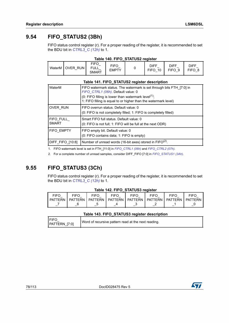
Register description LSM6DSL
78/113 DocID028475 Rev 5
9.54 FIFO_STATUS2 (3Bh)FIFO status control register (r). For a proper reading of the register, it is recommended to set the BDU bit in CTRL3_C (12h) to 1.
Table 140. FIFO_STATUS2 register
Table 141. FIFO_STATUS2 register description
9.55 FIFO_STATUS3 (3Ch)FIFO status control register (r). For a proper reading of the register, it is recommended to set the BDU bit in CTRL3_C (12h) to 1.
Table 142. FIFO_STATUS3 register
Table 143. FIFO_STATUS3 register description
WaterM OVER_RUNFIFO_FULL_SMART
FIFO_EMPTY 0 DIFF_
FIFO_10DIFF_
FIFO_9DIFF_
FIFO_8
WaterM FIFO watermark status. The watermark is set through bits FTH_[7:0] in FIFO_CTRL1 (06h). Default value: 0(0: FIFO filling is lower than watermark level(1); 1: FIFO filling is equal to or higher than the watermark level)
1. FIFO watermark level is set in FTH_[11:0] in FIFO_CTRL1 (06h) and FIFO_CTRL2 (07h).
OVER_RUN FIFO overrun status. Default value: 0(0: FIFO is not completely filled; 1: FIFO is completely filled)
FIFO_FULL_SMART
Smart FIFO full status. Default value: 0(0: FIFO is not full; 1: FIFO will be full at the next ODR)
FIFO_EMPTY FIFO empty bit. Default value: 0(0: FIFO contains data; 1: FIFO is empty)
DIFF_FIFO_[10:8] Number of unread words (16-bit axes) stored in FIFO(2).
2. For a complete number of unread samples, consider DIFF_FIFO [7:0] in FIFO_STATUS1 (3Ah).
FIFO_PATTERN
_7
FIFO_PATTERN
_6
FIFO_PATTERN
_5
FIFO_PATTERN
_4
FIFO_PATTERN
_3
FIFO_PATTERN
_2
FIFO_PATTERN
_1
FIFO_PATTERN
_0
FIFO_PATTERN_[7:0] Word of recursive pattern read at the next reading.
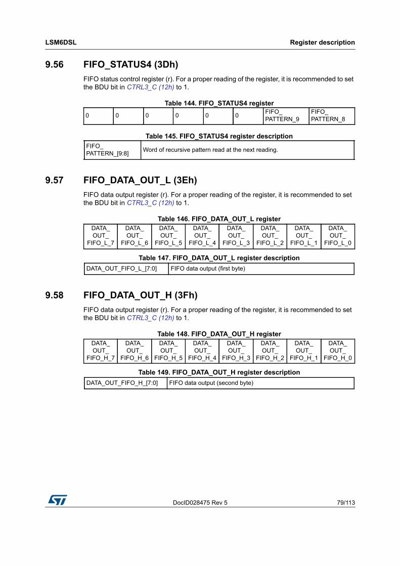
DocID028475 Rev 5 79/113
LSM6DSL Register description
113
9.56 FIFO_STATUS4 (3Dh)FIFO status control register (r). For a proper reading of the register, it is recommended to set the BDU bit in CTRL3_C (12h) to 1.
Table 144. FIFO_STATUS4 register
Table 145. FIFO_STATUS4 register description
9.57 FIFO_DATA_OUT_L (3Eh) FIFO data output register (r). For a proper reading of the register, it is recommended to set the BDU bit in CTRL3_C (12h) to 1.
9.58 FIFO_DATA_OUT_H (3Fh)FIFO data output register (r). For a proper reading of the register, it is recommended to set the BDU bit in CTRL3_C (12h) to 1.
0 0 0 0 0 0 FIFO_PATTERN_9
FIFO_PATTERN_8
FIFO_PATTERN_[9:8] Word of recursive pattern read at the next reading.
Table 146. FIFO_DATA_OUT_L registerDATA_OUT_
FIFO_L_7
DATA_OUT_
FIFO_L_6
DATA_OUT_
FIFO_L_5
DATA_OUT_
FIFO_L_4
DATA_OUT_
FIFO_L_3
DATA_OUT_
FIFO_L_2
DATA_OUT_
FIFO_L_1
DATA_OUT_
FIFO_L_0
Table 147. FIFO_DATA_OUT_L register descriptionDATA_OUT_FIFO_L_[7:0] FIFO data output (first byte)
Table 148. FIFO_DATA_OUT_H registerDATA_OUT_
FIFO_H_7
DATA_OUT_
FIFO_H_6
DATA_OUT_
FIFO_H_5
DATA_OUT_
FIFO_H_4
DATA_OUT_
FIFO_H_3
DATA_OUT_
FIFO_H_2
DATA_OUT_
FIFO_H_1
DATA_OUT_
FIFO_H_0
Table 149. FIFO_DATA_OUT_H register descriptionDATA_OUT_FIFO_H_[7:0] FIFO data output (second byte)
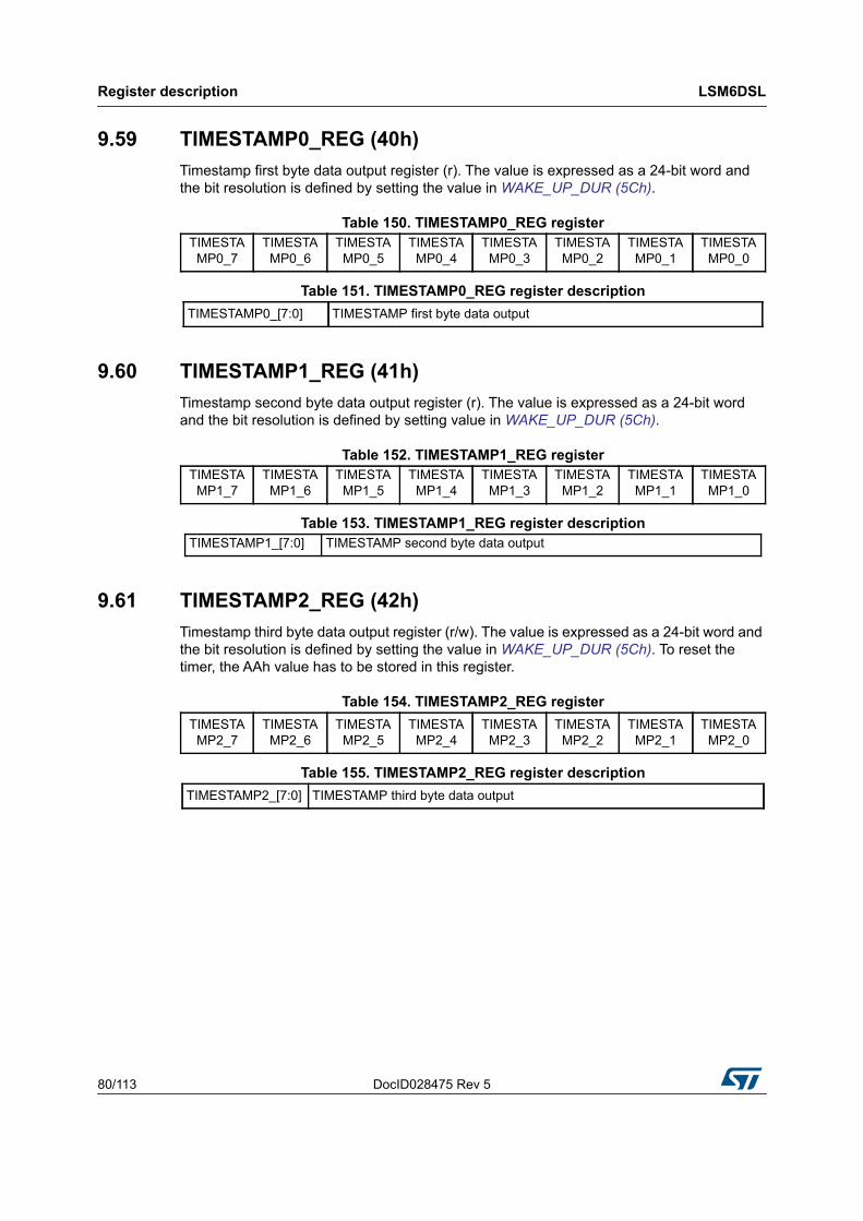
Register description LSM6DSL
80/113 DocID028475 Rev 5
9.59 TIMESTAMP0_REG (40h)Timestamp first byte data output register (r). The value is expressed as a 24-bit word and the bit resolution is defined by setting the value in WAKE_UP_DUR (5Ch).
9.60 TIMESTAMP1_REG (41h)Timestamp second byte data output register (r). The value is expressed as a 24-bit word and the bit resolution is defined by setting value in WAKE_UP_DUR (5Ch).
9.61 TIMESTAMP2_REG (42h)Timestamp third byte data output register (r/w). The value is expressed as a 24-bit word and the bit resolution is defined by setting the value in WAKE_UP_DUR (5Ch). To reset the timer, the AAh value has to be stored in this register.
Table 150. TIMESTAMP0_REG registerTIMESTA
MP0_7TIMESTA
MP0_6TIMESTA
MP0_5TIMESTA
MP0_4TIMESTA
MP0_3TIMESTA
MP0_2TIMESTA
MP0_1TIMESTA
MP0_0
Table 151. TIMESTAMP0_REG register descriptionTIMESTAMP0_[7:0] TIMESTAMP first byte data output
Table 152. TIMESTAMP1_REG registerTIMESTA
MP1_7TIMESTA
MP1_6TIMESTA
MP1_5TIMESTA
MP1_4TIMESTA
MP1_3TIMESTA
MP1_2TIMESTA
MP1_1TIMESTA
MP1_0
Table 153. TIMESTAMP1_REG register descriptionTIMESTAMP1_[7:0] TIMESTAMP second byte data output
Table 154. TIMESTAMP2_REG registerTIMESTA
MP2_7TIMESTA
MP2_6TIMESTA
MP2_5TIMESTA
MP2_4TIMESTA
MP2_3TIMESTA
MP2_2TIMESTA
MP2_1TIMESTA
MP2_0
Table 155. TIMESTAMP2_REG register descriptionTIMESTAMP2_[7:0] TIMESTAMP third byte data output
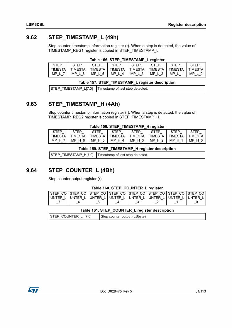
DocID028475 Rev 5 81/113
LSM6DSL Register description
113
9.62 STEP_TIMESTAMP_L (49h)Step counter timestamp information register (r). When a step is detected, the value of TIMESTAMP_REG1 register is copied in STEP_TIMESTAMP_L.
9.63 STEP_TIMESTAMP_H (4Ah)Step counter timestamp information register (r). When a step is detected, the value of TIMESTAMP_REG2 register is copied in STEP_TIMESTAMP_H.
9.64 STEP_COUNTER_L (4Bh)Step counter output register (r).
Table 156. STEP_TIMESTAMP_L registerSTEP_
TIMESTAMP_L_7
STEP_TIMESTAMP_L_6
STEP_TIMESTAMP_L_5
STEP_TIMESTAMP_L_4
STEP_TIMESTAMP_L_3
STEP_TIMESTAMP_L_2
STEP_TIMESTAMP_L_1
STEP_TIMESTAMP_L_0
Table 157. STEP_TIMESTAMP_L register descriptionSTEP_TIMESTAMP_L[7:0] Timestamp of last step detected.
Table 158. STEP_TIMESTAMP_H registerSTEP_
TIMESTAMP_H_7
STEP_TIMESTAMP_H_6
STEP_TIMESTAMP_H_5
STEP_TIMESTAMP_H_4
STEP_TIMESTAMP_H_3
STEP_TIMESTAMP_H_2
STEP_TIMESTAMP_H_1
STEP_TIMESTAMP_H_0
Table 159. STEP_TIMESTAMP_H register descriptionSTEP_TIMESTAMP_H[7:0] Timestamp of last step detected.
Table 160. STEP_COUNTER_L registerSTEP_COUNTER_L
_7
STEP_COUNTER_L
_6
STEP_COUNTER_L
_5
STEP_COUNTER_L
_4
STEP_COUNTER_L
_3
STEP_COUNTER_L
_2
STEP_COUNTER_L
_1
STEP_COUNTER_L
_0
Table 161. STEP_COUNTER_L register descriptionSTEP_COUNTER_L_[7:0] Step counter output (LSbyte)

Register description LSM6DSL
82/113 DocID028475 Rev 5
9.65 STEP_COUNTER_H (4Ch)Step counter output register (r).
9.66 SENSORHUB13_REG (4Dh)Thirteenth byte associated to external sensors. The content of the register is consistent with the SLAVEx_CONFIG number of read operation configurations (for external sensors from x = 0 to x = 3).
9.67 SENSORHUB14_REG (4Eh)Fourteenth byte associated to external sensors. The content of the register is consistent with the SLAVEx_CONFIG number of read operation configurations (for external sensors from x = 0 to x = 3).
9.68 SENSORHUB15_REG (4Fh)Fifteenth byte associated to external sensors. The content of the register is consistent with the SLAVEx_CONFIG number of read operation configurations (for external sensors from x = 0 to x = 3).
Table 162. STEP_COUNTER_H registerSTEP_COUNTER_H
_7
STEP_COUNTER_H
_6
STEP_COUNTER_H
_5
STEP_COUNTER_H
_4
STEP_COUNTER_H
_3
STEP_COUNTER_H
_2
STEP_COUNTER_H
_1
STEP_COUNTER_H
_0
Table 163. STEP_COUNTER_H register descriptionSTEP_COUNTER_H_[7:0] Step counter output (MSbyte)
Table 164. SENSORHUB13_REG registerSHub13_7 SHub13_6 SHub13_5 SHub13_4 SHub13_3 SHub13_2 SHub13_1 SHub13_0
Table 165. SENSORHUB13_REG register descriptionSHub13_[7:0] Thirteenth byte associated to external sensors
Table 166. SENSORHUB14_REG registerSHub14_7 SHub14_6 SHub14_5 SHub14_4 SHub14_3 SHub14_2 SHub14_1 SHub14_0
Table 167. SENSORHUB14_REG register descriptionSHub14_[7:0] Fourteenth byte associated to external sensors
Table 168. SENSORHUB15_REG registerSHub15_7 SHub15_6 SHub15_5 SHub15_4 SHub15_3 SHub15_2 SHub15_1 SHub15_0
Table 169. SENSORHUB15_REG register descriptionSHub15_[7:0] Fifteenth byte associated to external sensors
DocID028475 Rev 5 83/113
LSM6DSL Register description
113
9.69 SENSORHUB16_REG (50h)Sixteenth byte associated to external sensors. The content of the register is consistent with the SLAVEx_CONFIG number of read operation configurations (for external sensors from x = 0 to x = 3).
9.70 SENSORHUB17_REG (51h)Seventeenth byte associated to external sensors. The content of the register is consistent with the SLAVEx_CONFIG number of read operation configurations (for external sensors from x = 0 to x = 3).
9.71 SENSORHUB18_REG (52h)Eighteenth byte associated to external sensors. The content of the register is consistent with the SLAVEx_CONFIG number of read operation configurations (for external sensors from x = 0 to x = 3).
Table 170. SENSORHUB16_REG registerSHub16_7 SHub16_6 SHub16_5 SHub16_4 SHub16_3 SHub16_2 SHub16_1 SHub16_0
Table 171. SENSORHUB16_REG register descriptionSHub16_[7:0] Sixteenth byte associated to external sensors
Table 172. SENSORHUB17_REG registerSHub17_7 SHub17_6 SHub17_5 SHub17_4 SHub17_3 SHub17_2 SHub17_1 SHub17_0
Table 173. SENSORHUB17_REG register descriptionSHub17_[7:0] Seventeenth byte associated to external sensors
Table 174. SENSORHUB18_REG registerSHub18_7 SHub18_6 SHub18_5 SHub18_4 SHub18_3 SHub18_2 SHub18_1 SHub18_0
Table 175. SENSORHUB18_REG register descriptionSHub18_[7:0] Eighteenth byte associated to external sensors

Register description LSM6DSL
84/113 DocID028475 Rev 5
9.72 FUNC_SRC1 (53h)Significant motion, tilt, step detector, hard/soft-iron and sensor hub interrupt source register (r).
9.73 FUNC_SRC2 (54h)Wrist tilt interrupt source register (r).
Table 176. FUNC_SRC1 registerSTEP_COUNT_DELTA
_IA
SIGN_MOTION_IA TILT_IA STEP_
DETECTEDSTEP_
OVERFLOWHI_FAIL
SI_END_OP
SENSORHUB_
END_OP
Table 177. FUNC_SRC1 register description
STEP_COUNT_DELTA_IA
Pedometer step recognition on delta time status. Default value: 0(0: no step recognized during delta time; 1: at least one step recognized during delta time)
SIGN_MOTION_IA
Significant motion event detection status. Default value: 0(0: significant motion event not detected; 1: significant motion event detected)
TILT_IATilt event detection status. Default value: 0(0: tilt event not detected; 1: tilt event detected)
STEP_DETECTED
Step detector event detection status. Default value: 0(0: step detector event not detected; 1: step detector event detected)
STEP_OVERFLOW
Step counter overflow status. Default value: 0(0: step counter value < 216; 1: step counter value reached 216)
HI_FAIL Fail in hard/soft-ironing algorithm.
SI_END_OPHard/soft-iron calculation status. Default value: 0(0: Hard/soft-iron calculation not concluded; 1: Hard/soft-iron calculation concluded)
SENSORHUB_END_OP
Sensor hub communication status. Default value: 0(0: sensor hub communication not concluded; 1: sensor hub communication concluded)
Table 178. FUNC_SRC2 register
0 SLAVE3_NACK
SLAVE2_NACK
SLAVE1_NACK
SLAVE0_NACK 0 0 WRIST_
TILT_IA
Table 179. FUNC_SRC2 register description SLAVE3_NACK This bit is set to 1 if Not acknowledge occurs on slave 3 communication. Default value: 0
SLAVE2_NACK This bit is set to 1 if Not acknowledge occurs on slave 2 communication. Default value: 0
SLAVE1_NACK This bit is set to 1 if Not acknowledge occurs on slave 1 communication. Default value: 0
SLAVE0_NACK This bit is set to 1 if Not acknowledge occurs on slave 0 communication. Default value: 0
WRIST_TILT_IA Wrist tilt event detection status. Default value: 0 (0: Wrist tilt event not detected; 1: Wrist tilt event detected)
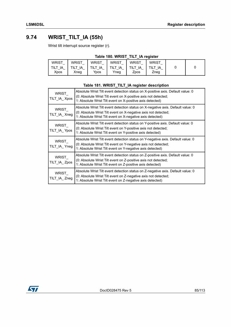
DocID028475 Rev 5 85/113
LSM6DSL Register description
113
9.74 WRIST_TILT_IA (55h)Wrist tilt interrupt source register (r).
Table 180. WRIST_TILT_IA registerWRIST_TILT_IA_
Xpos
WRIST_TILT_IA_
Xneg
WRIST_TILT_IA_
Ypos
WRIST_TILT_IA_
Yneg
WRIST_TILT_IA_
Zpos
WRIST_TILT_IA_
Zneg0 0
Table 181. WRIST_TILT_IA register description
WRIST_TILT_IA_ Xpos
Absolute Wrist Tilt event detection status on X-positive axis. Default value: 0(0: Absolute Wrist Tilt event on X-positive axis not detected; 1: Absolute Wrist Tilt event on X-positive axis detected)
WRIST_TILT_IA_ Xneg
Absolute Wrist Tilt event detection status on X-negative axis. Default value: 0(0: Absolute Wrist Tilt event on X-negative axis not detected; 1: Absolute Wrist Tilt event on X-negative axis detected)
WRIST_TILT_IA_ Ypos
Absolute Wrist Tilt event detection status on Y-positive axis. Default value: 0(0: Absolute Wrist Tilt event on Y-positive axis not detected; 1: Absolute Wrist Tilt event on Y-positive axis detected)
WRIST_TILT_IA_ Yneg
Absolute Wrist Tilt event detection status on Y-negative axis. Default value: 0(0: Absolute Wrist Tilt event on Y-negative axis not detected; 1: Absolute Wrist Tilt event on Y-negative axis detected)
WRIST_TILT_IA_ Zpos
Absolute Wrist Tilt event detection status on Z-positive axis. Default value: 0(0: Absolute Wrist Tilt event on Z-positive axis not detected; 1: Absolute Wrist Tilt event on Z-positive axis detected)
WRIST_TILT_IA_ Zneg
Absolute Wrist Tilt event detection status on Z-negative axis. Default value: 0(0: Absolute Wrist Tilt event on Z-negative axis not detected; 1: Absolute Wrist Tilt event on Z-negative axis detected)

Register description LSM6DSL
86/113 DocID028475 Rev 5
9.75 TAP_CFG (58h)Enables interrupt and inactivity functions, configuration of filtering and tap recognition functions (r/w).
Table 182. TAP_CFG registerINTERRUPTS
_ENABLE INACT_EN1 INACT_EN0 SLOPE_FDS TAP_X_EN TAP_Y_EN TAP_Z_EN LIR
Table 183. TAP_CFG register description INTERRUPTS_ENABLE
Enable basic interrupts (6D/4D, free-fall, wake-up, tap, inactivity). Default 0.(0: interrupt disabled; 1: interrupt enabled)
INACT_EN[1:0]
Enable inactivity function. Default value: 00(00: disabled01: sets accelerometer ODR to 12.5 Hz (low-power mode), gyro does not change;10: sets accelerometer ODR to 12.5 Hz (low-power mode), gyro to sleep mode;11: sets accelerometer ODR to 12.5 Hz (low-power mode), gyro to power-down mode)
SLOPE_FDSHPF or SLOPE filter selection on wake-up and Activity/Inactivity functions. Refer to Figure 8. Default value: 0 (0: SLOPE filter applied; 1: HPF applied)
TAP_X_ENEnable X direction in tap recognition. Default value: 0(0: X direction disabled; 1: X direction enabled)
TAP_Y_ENEnable Y direction in tap recognition. Default value: 0(0: Y direction disabled; 1: Y direction enabled)
TAP_Z_ENEnable Z direction in tap recognition. Default value: 0(0: Z direction disabled; 1: Z direction enabled)
LIRLatched Interrupt. Default value: 0(0: interrupt request not latched; 1: interrupt request latched)
DocID028475 Rev 5 87/113
LSM6DSL Register description
113
9.76 TAP_THS_6D (59h)Portrait/landscape position and tap function threshold register (r/w).
9.77 INT_DUR2 (5Ah)Tap recognition function setting register (r/w).
Table 184. TAP_THS_6D register
D4D_EN SIXD_THS1
SIXD_THS0
TAP_THS4
TAP_THS3
TAP_THS2
TAP_THS1
TAP_THS0
Table 185. TAP_THS_6D register description
D4D_EN4D orientation detection enable. Z-axis position detection is disabled.Default value: 0(0: enabled; 1: disabled)
SIXD_THS[1:0] Threshold for 4D/6D function. Default value: 00For details, refer to Table 186.
TAP_THS[4:0] Threshold for tap recognition. Default value: 00000 1 LSb corresponds to FS_XL/25
Table 186. Threshold for D4D/D6D functionSIXD_THS[1:0] Threshold value
00 80 degrees01 70 degrees10 60 degrees11 50 degrees
Table 187. INT_DUR2 registerDUR3 DUR2 DUR1 DUR0 QUIET1 QUIET0 SHOCK1 SHOCK0
Table 188. INT_DUR2 register description
DUR[3:0]
Duration of maximum time gap for double tap recognition. Default: 0000When double tap recognition is enabled, this register expresses the maximum time between two consecutive detected taps to determine a double tap event. The default value of these bits is 0000b which corresponds to 16*ODR_XL time. If the DUR[3:0] bits are set to a different value, 1LSB corresponds to 32*ODR_XL time.
QUIET[1:0]
Expected quiet time after a tap detection. Default value: 00Quiet time is the time after the first detected tap in which there must not be any overthreshold event. The default value of these bits is 00b which corresponds to 2*ODR_XL time. If the QUIET[1:0] bits are set to a different value, 1LSB corresponds to 4*ODR_XL time.
SHOCK[1:0]
Maximum duration of overthreshold event. Default value: 00Maximum duration is the maximum time of an overthreshold signal detection to be recognized as a tap event. The default value of these bits is 00b which corresponds to 4*ODR_XL time. If the SHOCK[1:0] bits are set to a different value, 1LSB corresponds to 8*ODR_XL time.
Register description LSM6DSL
88/113 DocID028475 Rev 5
9.78 WAKE_UP_THS (5Bh)Single and double-tap function threshold register (r/w).
9.79 WAKE_UP_DUR (5Ch)Free-fall, wakeup, timestamp and sleep mode functions duration setting register (r/w).
Table 189. WAKE_UP_THS registerSINGLE_DOUBLE
_TAP0 WK_THS5 WK_THS4 WK_THS3 WK_THS2 WK_THS1 WK_THS0
Table 190. WAKE_UP_THS register description
SINGLE_DOUBLE_TAPSingle/double-tap event enable. Default: 0(0: only single-tap event enabled; 1: both single and double-tap events enabled)
WK_THS[5:0] Threshold for wakeup. Default value: 000000 1 LSb corresponds to FS_XL/26
Table 191. WAKE_UP_DUR register
FF_DUR5 WAKE_DUR1
WAKE_DUR0
TIMER_HR
SLEEP_DUR3
SLEEP_DUR2
SLEEP_DUR1
SLEEP_DUR0
Table 192. WAKE_UP_DUR register description
FF_DUR5
Free fall duration event. Default: 0For the complete configuration of the free-fall duration, refer to FF_DUR[4:0] in FREE_FALL (5Dh) configuration.1 LSB = 1 ODR_time
WAKE_DUR[1:0]Wake up duration event. Default: 001LSB = 1 ODR_time
TIMER_HRTimestamp register resolution setting(1). Default value: 0(0: 1LSB = 6.4 ms; 1: 1LSB = 25 μs)
1. Configuration of this bit affects TIMESTAMP0_REG (40h), TIMESTAMP1_REG (41h), TIMESTAMP2_REG (42h), STEP_TIMESTAMP_L (49h), STEP_TIMESTAMP_H (4Ah), and CTRL6_C (15h) registers.
SLEEP_DUR[3:0]Duration to go in sleep mode. Default value: 0000 (this corresponds to 16 ODR)1 LSB = 512 ODR
DocID028475 Rev 5 89/113
LSM6DSL Register description
113
9.80 FREE_FALL (5Dh)Free-fall function duration setting register (r/w).
Table 193. FREE_FALL registerFF_DUR4 FF_DUR3 FF_DUR2 FF_DUR1 FF_DUR0 FF_THS2 FF_THS1 FF_THS0
Table 194. FREE_FALL register description
FF_DUR[4:0]Free-fall duration event. Default: 0For the complete configuration of the free fall duration, refer to FF_DUR5 in WAKE_UP_DUR (5Ch) configuration
FF_THS[2:0]Free fall threshold setting. Default: 000For details refer to Table 195.
Table 195. Threshold for free-fall function FF_THS[2:0] Threshold value
000 156 mg
001 219 mg
010 250 mg
011 312 mg
100 344 mg
101 406 mg
110 469 mg
111 500 mg
Register description LSM6DSL
90/113 DocID028475 Rev 5
9.81 MD1_CFG (5Eh)Functions routing on INT1 register (r/w).
Table 196. MD1_CFG registerINT1_
INACT_STATE
INT1_SINGLE_
TAPINT1_WU INT1_FF
INT1_DOUBLE_
TAPINT1_6D INT1_TILT INT1_
TIMER
Table 197. MD1_CFG register description INT1_INACT_STATE
Routing on INT1 of inactivity mode. Default: 0(0: routing on INT1 of inactivity disabled; 1: routing on INT1 of inactivity enabled)
INT1_SINGLE_TAP
Single-tap recognition routing on INT1. Default: 0(0: routing of single-tap event on INT1 disabled; 1: routing of single-tap event on INT1 enabled)
INT1_WURouting of wakeup event on INT1. Default value: 0(0: routing of wakeup event on INT1 disabled; 1: routing of wakeup event on INT1 enabled)
INT1_FFRouting of free-fall event on INT1. Default value: 0(0: routing of free-fall event on INT1 disabled; 1: routing of free-fall event on INT1 enabled)
INT1_DOUBLE_TAP
Routing of tap event on INT1. Default value: 0(0: routing of double-tap event on INT1 disabled; 1: routing of double-tap event on INT1 enabled)
INT1_6DRouting of 6D event on INT1. Default value: 0(0: routing of 6D event on INT1 disabled; 1: routing of 6D event on INT1 enabled)
INT1_TILTRouting of tilt event on INT1. Default value: 0(0: routing of tilt event on INT1 disabled; 1: routing of tilt event on INT1 enabled)
INT1_TIMERRouting of end counter event of timer on INT1. Default value: 0(0: routing of end counter event of timer on INT1 disabled; 1: routing of end counter event of timer event on INT1 enabled)
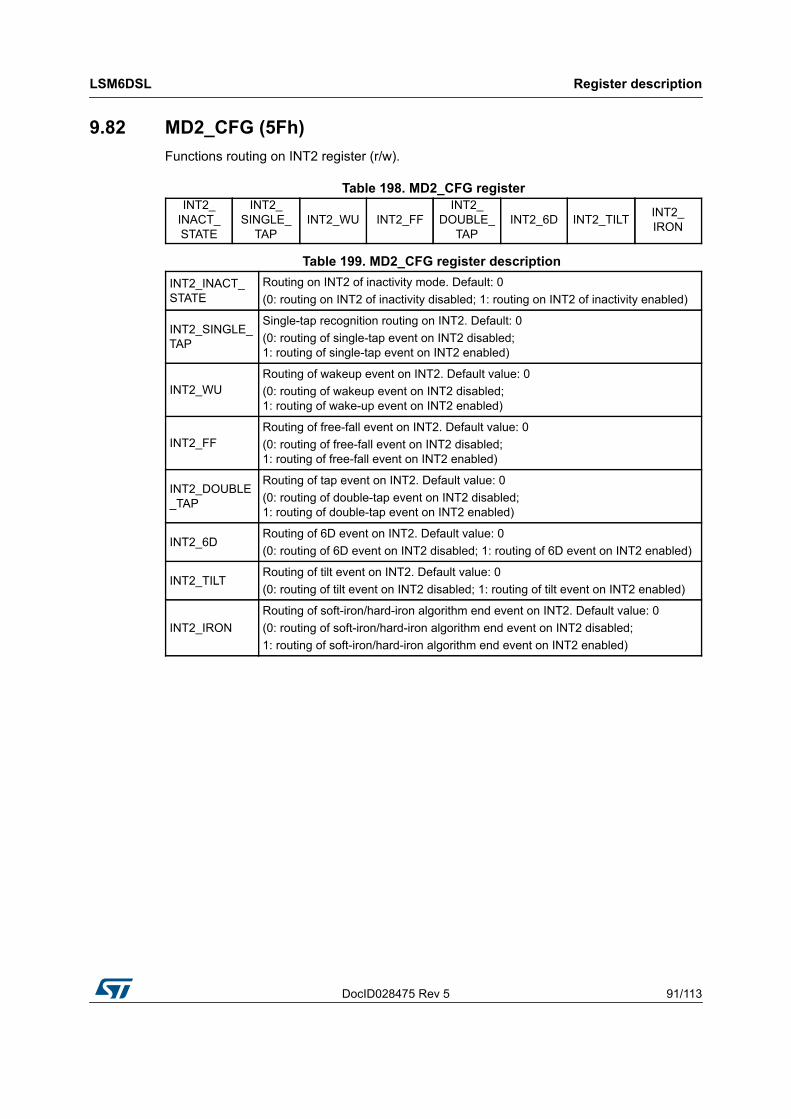
DocID028475 Rev 5 91/113
LSM6DSL Register description
113
9.82 MD2_CFG (5Fh)Functions routing on INT2 register (r/w).
Table 198. MD2_CFG registerINT2_
INACT_STATE
INT2_SINGLE_
TAPINT2_WU INT2_FF
INT2_DOUBLE_
TAPINT2_6D INT2_TILT INT2_
IRON
Table 199. MD2_CFG register description INT2_INACT_STATE
Routing on INT2 of inactivity mode. Default: 0(0: routing on INT2 of inactivity disabled; 1: routing on INT2 of inactivity enabled)
INT2_SINGLE_TAP
Single-tap recognition routing on INT2. Default: 0(0: routing of single-tap event on INT2 disabled; 1: routing of single-tap event on INT2 enabled)
INT2_WURouting of wakeup event on INT2. Default value: 0(0: routing of wakeup event on INT2 disabled; 1: routing of wake-up event on INT2 enabled)
INT2_FFRouting of free-fall event on INT2. Default value: 0(0: routing of free-fall event on INT2 disabled; 1: routing of free-fall event on INT2 enabled)
INT2_DOUBLE_TAP
Routing of tap event on INT2. Default value: 0(0: routing of double-tap event on INT2 disabled; 1: routing of double-tap event on INT2 enabled)
INT2_6DRouting of 6D event on INT2. Default value: 0(0: routing of 6D event on INT2 disabled; 1: routing of 6D event on INT2 enabled)
INT2_TILTRouting of tilt event on INT2. Default value: 0(0: routing of tilt event on INT2 disabled; 1: routing of tilt event on INT2 enabled)
INT2_IRONRouting of soft-iron/hard-iron algorithm end event on INT2. Default value: 0(0: routing of soft-iron/hard-iron algorithm end event on INT2 disabled;1: routing of soft-iron/hard-iron algorithm end event on INT2 enabled)
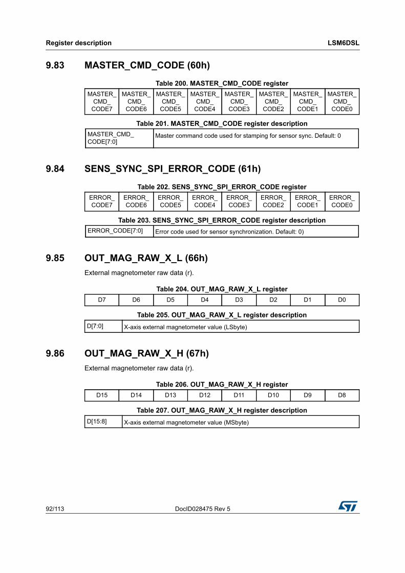
Register description LSM6DSL
92/113 DocID028475 Rev 5
9.83 MASTER_CMD_CODE (60h)
9.84 SENS_SYNC_SPI_ERROR_CODE (61h)
9.85 OUT_MAG_RAW_X_L (66h)External magnetometer raw data (r).
9.86 OUT_MAG_RAW_X_H (67h)External magnetometer raw data (r).
Table 200. MASTER_CMD_CODE registerMASTER_
CMD_CODE7
MASTER_CMD_
CODE6
MASTER_CMD_
CODE5
MASTER_CMD_
CODE4
MASTER_CMD_
CODE3
MASTER_CMD_
CODE2
MASTER_CMD_
CODE1
MASTER_CMD_
CODE0
Table 201. MASTER_CMD_CODE register descriptionMASTER_CMD_CODE[7:0]
Master command code used for stamping for sensor sync. Default: 0
Table 202. SENS_SYNC_SPI_ERROR_CODE registerERROR_CODE7
ERROR_CODE6
ERROR_CODE5
ERROR_CODE4
ERROR_CODE3
ERROR_CODE2
ERROR_CODE1
ERROR_CODE0
Table 203. SENS_SYNC_SPI_ERROR_CODE register descriptionERROR_CODE[7:0] Error code used for sensor synchronization. Default: 0)
Table 204. OUT_MAG_RAW_X_L registerD7 D6 D5 D4 D3 D2 D1 D0
Table 205. OUT_MAG_RAW_X_L register descriptionD[7:0] X-axis external magnetometer value (LSbyte)
Table 206. OUT_MAG_RAW_X_H registerD15 D14 D13 D12 D11 D10 D9 D8
Table 207. OUT_MAG_RAW_X_H register descriptionD[15:8] X-axis external magnetometer value (MSbyte)
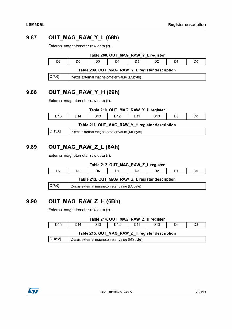
DocID028475 Rev 5 93/113
LSM6DSL Register description
113
9.87 OUT_MAG_RAW_Y_L (68h)External magnetometer raw data (r).
9.88 OUT_MAG_RAW_Y_H (69h)External magnetometer raw data (r).
9.89 OUT_MAG_RAW_Z_L (6Ah)External magnetometer raw data (r).
9.90 OUT_MAG_RAW_Z_H (6Bh)External magnetometer raw data (r).
Table 208. OUT_MAG_RAW_Y_L registerD7 D6 D5 D4 D3 D2 D1 D0
Table 209. OUT_MAG_RAW_Y_L register descriptionD[7:0] Y-axis external magnetometer value (LSbyte)
Table 210. OUT_MAG_RAW_Y_H registerD15 D14 D13 D12 D11 D10 D9 D8
Table 211. OUT_MAG_RAW_Y_H register descriptionD[15:8] Y-axis external magnetometer value (MSbyte)
Table 212. OUT_MAG_RAW_Z_L registerD7 D6 D5 D4 D3 D2 D1 D0
Table 213. OUT_MAG_RAW_Z_L register descriptionD[7:0] Z-axis external magnetometer value (LSbyte)
Table 214. OUT_MAG_RAW_Z_H registerD15 D14 D13 D12 D11 D10 D9 D8
Table 215. OUT_MAG_RAW_Z_H register descriptionD[15:8] Z-axis external magnetometer value (MSbyte)
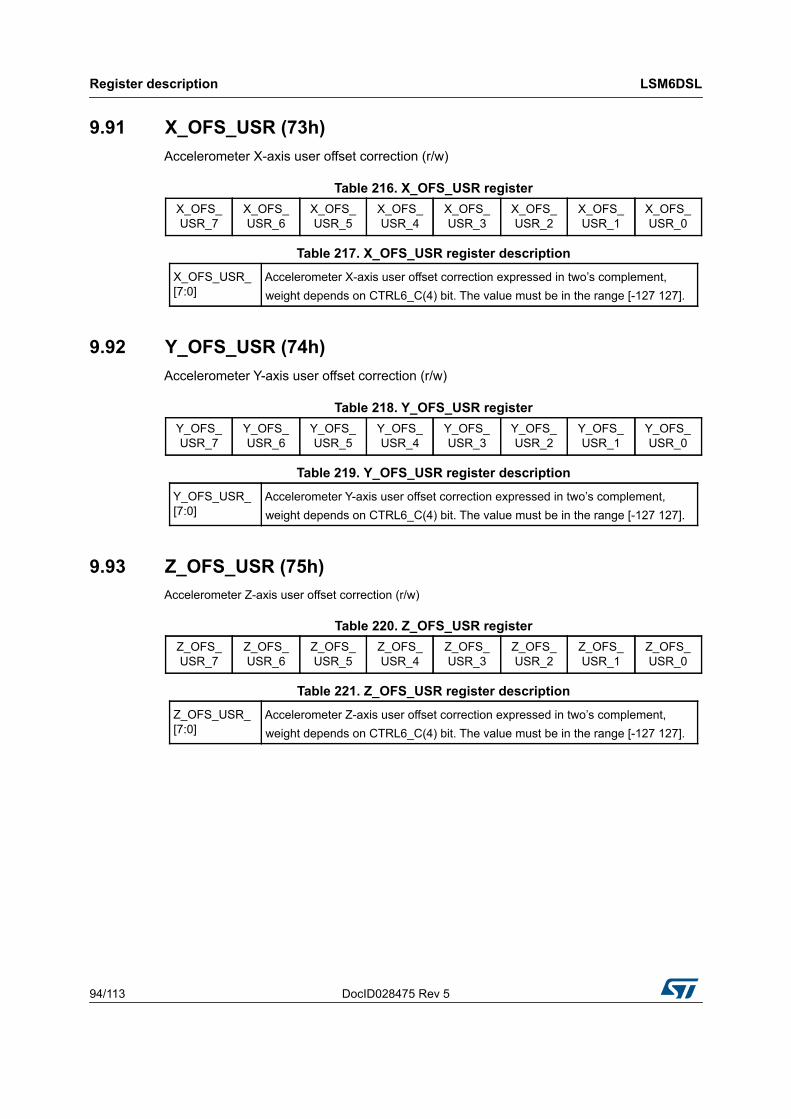
Register description LSM6DSL
94/113 DocID028475 Rev 5
9.91 X_OFS_USR (73h)Accelerometer X-axis user offset correction (r/w)
9.92 Y_OFS_USR (74h)Accelerometer Y-axis user offset correction (r/w)
9.93 Z_OFS_USR (75h)Accelerometer Z-axis user offset correction (r/w)
Table 216. X_OFS_USR registerX_OFS_USR_7
X_OFS_USR_6
X_OFS_USR_5
X_OFS_USR_4
X_OFS_USR_3
X_OFS_USR_2
X_OFS_USR_1
X_OFS_USR_0
Table 217. X_OFS_USR register descriptionX_OFS_USR_[7:0]
Accelerometer X-axis user offset correction expressed in two’s complement, weight depends on CTRL6_C(4) bit. The value must be in the range [-127 127].
Table 218. Y_OFS_USR registerY_OFS_USR_7
Y_OFS_USR_6
Y_OFS_USR_5
Y_OFS_USR_4
Y_OFS_USR_3
Y_OFS_USR_2
Y_OFS_USR_1
Y_OFS_USR_0
Table 219. Y_OFS_USR register descriptionY_OFS_USR_[7:0]
Accelerometer Y-axis user offset correction expressed in two’s complement, weight depends on CTRL6_C(4) bit. The value must be in the range [-127 127].
Table 220. Z_OFS_USR registerZ_OFS_USR_7
Z_OFS_USR_6
Z_OFS_USR_5
Z_OFS_USR_4
Z_OFS_USR_3
Z_OFS_USR_2
Z_OFS_USR_1
Z_OFS_USR_0
Table 221. Z_OFS_USR register descriptionZ_OFS_USR_[7:0]
Accelerometer Z-axis user offset correction expressed in two’s complement, weight depends on CTRL6_C(4) bit. The value must be in the range [-127 127].
DocID028475 Rev 5 95/113
LSM6DSL Embedded functions register mapping
113
10 Embedded functions register mapping
The tables given below provide a list of the first (A) and second (B) bank registers related to the embedded functions available in the device and the corresponding addresses.
The embedded functions registers of bank A are accessible when FUNC_CFG_EN is set to ‘1’ in FUNC_CFG_ACCESS (01h).
The embedded functions registers of bank B are accessible when both FUNC_CFG_EN and FUNC_CFG_EN_B set to ‘1’ in FUNC_CFG_ACCESS (01h).
Note: All modifications of the content of the embedded functions registers have to be performed with the device in power-down mode.
Table 222. Register address map - Bank A - embedded functions
Name TypeRegister address
Default CommentHex Binary
SLV0_ADD r/w 02 00000010 00000000
SLV0_SUBADD r/w 03 00000011 00000000
SLAVE0_CONFIG r/w 04 00000100 00000000
SLV1_ADD r/w 05 00000101 00000000
SLV1_SUBADD r/w 06 00000110 00000000
SLAVE1_CONFIG r/w 07 00000111 00000000
SLV2_ADD r/w 08 00001000 00000000
SLV2_SUBADD r/w 09 00001001 00000000
SLAVE2_CONFIG r/w 0A 00001010 00000000
SLV3_ADD r/w 0B 00001011 00000000
SLV3_SUBADD r/w 0C 00001100 00000000
SLAVE3_CONFIG r/w 0D 00001101 00000000
DATAWRITE_SRC_MODE_SUB_SLV0 r/w 0E 00001110 00000000
CONFIG_PEDO_THS_MIN r/w 0F 00001111 00010000
RESERVED - 10-12 Reserved
SM_THS r/w 13 00010011 00000110
PEDO_DEB_REG r/w 14 00010100 01101110
STEP_COUNT_DELTA r/w 15 0001 0101 00000000
MAG_SI_XX r/w 24 00100100 00001000
MAG_SI_XY r/w 25 00100101 00000000
MAG_SI_XZ r/w 26 00100110 00000000
MAG_SI_YX r/w 27 00100111 00000000
MAG_SI_YY r/w 28 00101000 00001000
Embedded functions register mapping LSM6DSL
96/113 DocID028475 Rev 5
Registers marked as Reserved must not be changed. Writing to those registers may cause permanent damage to the device.
The content of the registers that are loaded at boot should not be changed. They contain the factory calibration values. Their content is automatically restored when the device is powered up.
MAG_SI_YZ r/w 29 00101001 00000000
MAG_SI_ZX r/w 2A 00101010 00000000
MAG_SI_ZY r/w 2B 00101011 00000000
MAG_SI_ZZ r/w 2C 00101100 00001000
MAG_OFFX_L r/w 2D 00101101 00000000
MAG_OFFX_H r/w 2E 00101110 00000000
MAG_OFFY_L r/w 2F 00101111 00000000
MAG_OFFY_H r/w 30 00110000 00000000
MAG_OFFZ_L r/w 31 00110001 00000000
MAG_OFFZ_H r/w 32 00110010 00000000
Table 223. Register address map - Bank B - embedded functions
Name TypeRegister address
Default CommentHex Binary
A_WRIST_TILT_LAT r/w 50 01010000 00001111
RESERVED - 51-53 Reserved
A_WRIST_TILT_THS r/w 54 01010100 00100000
RESERVED - 55-58 Reserved
A_WRIST_TILT_Mask r/w 59 01011001 11000000
Table 222. Register address map - Bank A - embedded functions (continued)
Name TypeRegister address
Default CommentHex Binary
DocID028475 Rev 5 97/113
LSM6DSL Embedded functions registers description - Bank A
113
11 Embedded functions registers description - Bank A
Note: All modifications of the content of the embedded functions registers have to be performed with the device in power-down mode.
11.1 SLV0_ADD (02h)I2C slave address of the first external sensor (Sensor1) register (r/w).
11.2 SLV0_SUBADD (03h)Address of register on the first external sensor (Sensor1) register (r/w).
11.3 SLAVE0_CONFIG (04h)First external sensor (Sensor1) configuration and sensor hub settings register (r/w).
Table 224. SLV0_ADD registerSlave0_
add6Slave0_
add5Slave0_
add4Slave0_
add3Slave0_
add2Slave0_
add1Slave0_
add0 rw_0
Table 225. SLV0_ADD register description
Slave0_add[6:0]I2C slave address of Sensor1 that can be read by sensor hub. Default value: 0000000
rw_0Read/write operation on Sensor1. Default value: 0(0: write operation; 1: read operation)
Table 226. SLV0_SUBADD registerSlave0_
reg7Slave0_
reg6Slave0_
reg5Slave0_
reg4Slave0_
reg3Slave0_
reg2Slave0_
reg1Slave0_
reg0
Table 227. SLV0_SUBADD register description
Slave0_reg[7:0] Address of register on Sensor1 that has to be read/write according to the rw_0 bit value in SLV0_ADD (02h). Default value: 00000000
Table 228. SLAVE0_CONFIG registerSlave0_
rate1Slave0_
rate0Aux_sens
_on1Aux_sens
_on0 Src_mode Slave0_numop2
Slave0_numop1
Slave0_numop0
Embedded functions registers description - Bank A LSM6DSL
98/113 DocID028475 Rev 5
11.4 SLV1_ADD (05h)I2C slave address of the second external sensor (Sensor2) register (r/w).
11.5 SLV1_SUBADD (06h)Address of register on the second external sensor (Sensor2) register (r/w).
Table 229. SLAVE0_CONFIG register description
Slave0_rate[1:0]
Decimation of read operation on Sensor1 starting from the sensor hub trigger. Default value: 00(00: no decimation01: update every 2 samples10: update every 4 samples11: update every 8 samples)
Aux_sens_on[1:0]
Number of external sensors to be read by sensor hub. Default value: 00(00: one sensor01: two sensors10: three sensors11: four sensors)
Src_modeSource mode conditioned read(1). Default value: 0(0: source mode read disabled; 1: source mode read enabled)
Slave0_numop[2:0] Number of read operations on Sensor1.
1. Read conditioned by the content of the register at address specified in the DATAWRITE_SRC_MODE_SUB_SLV0 (0Eh)register. If the content is non-zero, the operation continues with the reading of the address specified in the SLV0_SUBADD (03h) register, else the operation is interrupted.
Table 230. SLV1_ADD registerSlave1_
add6Slave1_
add5Slave1_
add4Slave1_
add3Slave1_
add2Slave1_
add1Slave1_
add0 r_1
Table 231. SLV1_ADD register description
Slave1_add[6:0]I2C slave address of Sensor2 that can be read by sensor hub. Default value: 0000000
r_1Read operation on Sensor2 enable. Default value: 0 (0: read operation disabled; 1: read operation enabled)
Table 232. SLV1_SUBADD registerSlave1_
reg7Slave1_
reg6Slave1_
reg5Slave1_
reg4Slave1_
reg3Slave1_
reg2Slave1_
reg1Slave1_
reg0
Table 233. SLV1_SUBADD register description
Slave1_reg[7:0] Address of register on Sensor2 that has to be read according to the r_1 bit value in SLV1_ADD (05h). Default value: 00000000
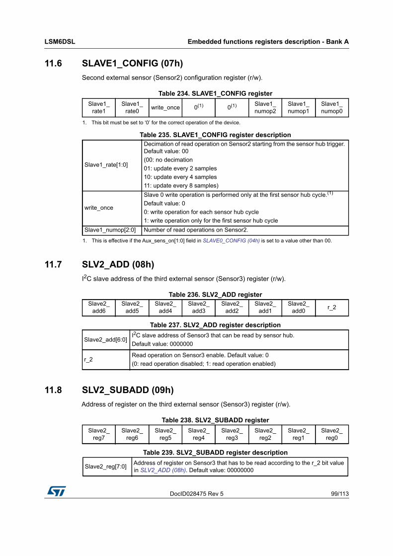
DocID028475 Rev 5 99/113
LSM6DSL Embedded functions registers description - Bank A
113
11.6 SLAVE1_CONFIG (07h)Second external sensor (Sensor2) configuration register (r/w).
11.7 SLV2_ADD (08h)I2C slave address of the third external sensor (Sensor3) register (r/w).
11.8 SLV2_SUBADD (09h)Address of register on the third external sensor (Sensor3) register (r/w).
Table 234. SLAVE1_CONFIG registerSlave1_
rate1Slave1_
rate0 write_once 0(1)
1. This bit must be set to ‘0’ for the correct operation of the device.
0(1) Slave1_numop2
Slave1_numop1
Slave1_numop0
Table 235. SLAVE1_CONFIG register description
Slave1_rate[1:0]
Decimation of read operation on Sensor2 starting from the sensor hub trigger. Default value: 00(00: no decimation01: update every 2 samples10: update every 4 samples11: update every 8 samples)
write_once
Slave 0 write operation is performed only at the first sensor hub cycle.(1)
Default value: 00: write operation for each sensor hub cycle1: write operation only for the first sensor hub cycle
1. This is effective if the Aux_sens_on[1:0] field in SLAVE0_CONFIG (04h) is set to a value other than 00.
Slave1_numop[2:0] Number of read operations on Sensor2.
Table 236. SLV2_ADD registerSlave2_
add6Slave2_
add5Slave2_
add4Slave2_
add3Slave2_
add2Slave2_
add1Slave2_
add0 r_2
Table 237. SLV2_ADD register description
Slave2_add[6:0]I2C slave address of Sensor3 that can be read by sensor hub. Default value: 0000000
r_2Read operation on Sensor3 enable. Default value: 0(0: read operation disabled; 1: read operation enabled)
Table 238. SLV2_SUBADD registerSlave2_
reg7Slave2_
reg6Slave2_
reg5Slave2_
reg4Slave2_
reg3Slave2_
reg2Slave2_
reg1Slave2_
reg0
Table 239. SLV2_SUBADD register description
Slave2_reg[7:0] Address of register on Sensor3 that has to be read according to the r_2 bit value in SLV2_ADD (08h). Default value: 00000000
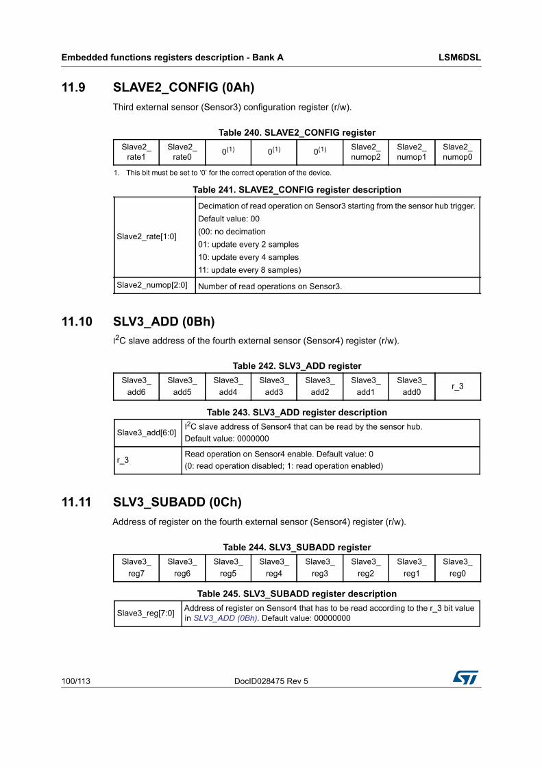
Embedded functions registers description - Bank A LSM6DSL
100/113 DocID028475 Rev 5
11.9 SLAVE2_CONFIG (0Ah)Third external sensor (Sensor3) configuration register (r/w).
11.10 SLV3_ADD (0Bh)I2C slave address of the fourth external sensor (Sensor4) register (r/w).
11.11 SLV3_SUBADD (0Ch)Address of register on the fourth external sensor (Sensor4) register (r/w).
Table 240. SLAVE2_CONFIG registerSlave2_
rate1Slave2_
rate0 0(1)
1. This bit must be set to ‘0’ for the correct operation of the device.
0(1) 0(1) Slave2_numop2
Slave2_numop1
Slave2_numop0
Table 241. SLAVE2_CONFIG register description
Slave2_rate[1:0]
Decimation of read operation on Sensor3 starting from the sensor hub trigger. Default value: 00(00: no decimation01: update every 2 samples10: update every 4 samples11: update every 8 samples)
Slave2_numop[2:0] Number of read operations on Sensor3.
Table 242. SLV3_ADD registerSlave3_
add6Slave3_
add5Slave3_
add4Slave3_
add3Slave3_
add2Slave3_
add1Slave3_
add0r_3
Table 243. SLV3_ADD register description
Slave3_add[6:0]I2C slave address of Sensor4 that can be read by the sensor hub. Default value: 0000000
r_3Read operation on Sensor4 enable. Default value: 0 (0: read operation disabled; 1: read operation enabled)
Table 244. SLV3_SUBADD registerSlave3_
reg7Slave3_
reg6Slave3_
reg5Slave3_
reg4Slave3_
reg3Slave3_
reg2Slave3_
reg1Slave3_
reg0
Table 245. SLV3_SUBADD register description
Slave3_reg[7:0] Address of register on Sensor4 that has to be read according to the r_3 bit value in SLV3_ADD (0Bh). Default value: 00000000
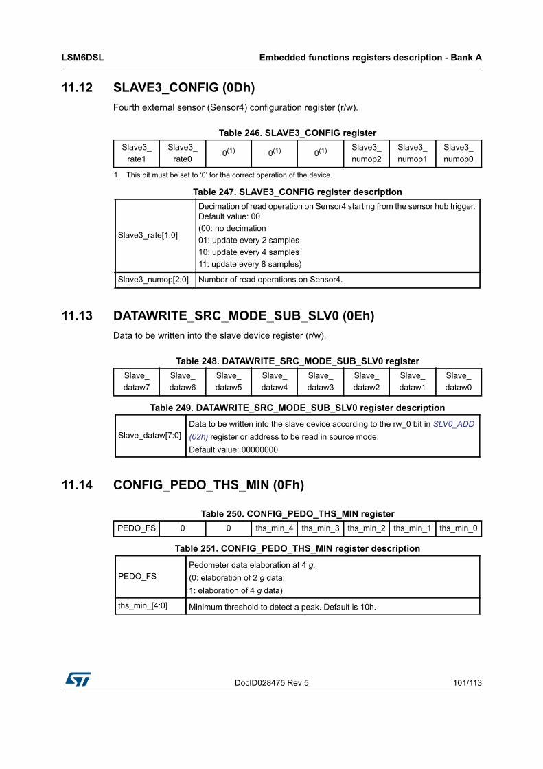
DocID028475 Rev 5 101/113
LSM6DSL Embedded functions registers description - Bank A
113
11.12 SLAVE3_CONFIG (0Dh)Fourth external sensor (Sensor4) configuration register (r/w).
11.13 DATAWRITE_SRC_MODE_SUB_SLV0 (0Eh)Data to be written into the slave device register (r/w).
11.14 CONFIG_PEDO_THS_MIN (0Fh)
Table 246. SLAVE3_CONFIG registerSlave3_
rate1Slave3_
rate00(1)
1. This bit must be set to ‘0’ for the correct operation of the device.
0(1) 0(1) Slave3_numop2
Slave3_numop1
Slave3_numop0
Table 247. SLAVE3_CONFIG register description
Slave3_rate[1:0]
Decimation of read operation on Sensor4 starting from the sensor hub trigger. Default value: 00(00: no decimation01: update every 2 samples10: update every 4 samples11: update every 8 samples)
Slave3_numop[2:0] Number of read operations on Sensor4.
Table 248. DATAWRITE_SRC_MODE_SUB_SLV0 registerSlave_dataw7
Slave_dataw6
Slave_dataw5
Slave_dataw4
Slave_dataw3
Slave_dataw2
Slave_dataw1
Slave_dataw0
Table 249. DATAWRITE_SRC_MODE_SUB_SLV0 register description
Slave_dataw[7:0]Data to be written into the slave device according to the rw_0 bit in SLV0_ADD (02h) register or address to be read in source mode.Default value: 00000000
Table 250. CONFIG_PEDO_THS_MIN registerPEDO_FS 0 0 ths_min_4 ths_min_3 ths_min_2 ths_min_1 ths_min_0
Table 251. CONFIG_PEDO_THS_MIN register description
PEDO_FSPedometer data elaboration at 4 g.(0: elaboration of 2 g data;1: elaboration of 4 g data)
ths_min_[4:0] Minimum threshold to detect a peak. Default is 10h.
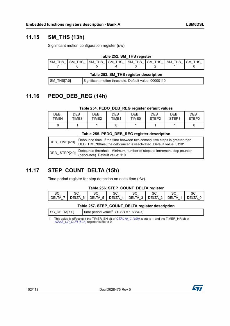
Embedded functions registers description - Bank A LSM6DSL
102/113 DocID028475 Rev 5
11.15 SM_THS (13h)Significant motion configuration register (r/w).
11.16 PEDO_DEB_REG (14h)
11.17 STEP_COUNT_DELTA (15h)Time period register for step detection on delta time (r/w).
Table 252. SM_THS registerSM_THS_
7SM_THS_
6SM_THS_
5SM_THS_
4SM_THS_
3SM_THS_
2SM_THS_
1SM_THS_
0
Table 253. SM_THS register descriptionSM_THS[7:0] Significant motion threshold. Default value: 00000110
Table 254. PEDO_DEB_REG register default valuesDEB_ TIME4
DEB_ TIME3
DEB_ TIME2
DEB_ TIME1
DEB_ TIME0
DEB_ STEP2
DEB_ STEP1
DEB_ STEP0
0 1 1 0 1 1 1 0
Table 255. PEDO_DEB_REG register description
DEB_ TIME[4:0] Debounce time. If the time between two consecutive steps is greater than DEB_TIME*80ms, the debouncer is reactivated. Default value: 01101
DEB_ STEP[2:0] Debounce threshold. Minimum number of steps to increment step counter (debounce). Default value: 110
Table 256. STEP_COUNT_DELTA registerSC_
DELTA_7SC_
DELTA_6SC_
DELTA_5SC_
DELTA_4SC_
DELTA_3SC_
DELTA_2SC_
DELTA_1SC_
DELTA_0
Table 257. STEP_COUNT_DELTA register descriptionSC_DELTA[7:0] Time period value(1) (1LSB = 1.6384 s)
1. This value is effective if the TIMER_EN bit of CTRL10_C (19h) is set to 1 and the TIMER_HR bit of WAKE_UP_DUR (5Ch) register is set to 0.

DocID028475 Rev 5 103/113
LSM6DSL Embedded functions registers description - Bank A
113
11.18 MAG_SI_XX (24h)Soft-iron matrix correction register (r/w).
11.19 MAG_SI_XY (25h)Soft-iron matrix correction register (r/w).
11.20 MAG_SI_XZ (26h)Soft-iron matrix correction register (r/w).
11.21 MAG_SI_YX (27h)Soft-iron matrix correction register (r/w).
Table 258. MAG_SI_XX registerMAG_SI_
XX_7MAG_SI_
XX_6MAG_SI_
XX_5MAG_SI_
XX_4MAG_SI_
XX_3MAG_SI_
XX_2MAG_SI_
XX_1MAG_SI_
XX_0
Table 259. MAG_SI_XX register descriptionMAG_SI_XX_[7:0] Soft-iron correction row1 col1 coefficient(1). Default value: 00001000
1. Value is expressed in sign-module format.
Table 260. MAG_SI_XY registerMAG_SI_
XY_7MAG_SI_
XY_6MAG_SI_
XY_5MAG_SI_
XY_4MAG_SI_
XY_3MAG_SI_
XY_2MAG_SI_
XY_1MAG_SI_
XY_0
Table 261. MAG_SI_XY register descriptionMAG_SI_XY_[7:0] Soft-iron correction row1 col2 coefficient(1). Default value: 00000000
1. Value is expressed in sign-module format.
Table 262. MAG_SI_XZ registerMAG_SI_
XZ_7MAG_SI_
XZ_6MAG_SI_
XZ_5MAG_SI_
XZ_4MAG_SI_
XZ_3MAG_SI_
XZ_2MAG_SI_
XZ_1MAG_SI_
XZ_0
Table 263. MAG_SI_XZ register descriptionMAG_SI_XZ_[7:0] Soft-iron correction row1 col3 coefficient(1). Default value: 00000000
1. Value is expressed in sign-module format.
Table 264. MAG_SI_YX registerMAG_SI_
YX_7MAG_SI_
YX_6MAG_SI_
YX_5MAG_SI_
YX_4MAG_SI_
YX_3MAG_SI_
YX_2MAG_SI_
YX_1MAG_SI_
YX_0
Table 265. MAG_SI_YX register descriptionMAG_SI_YX_[7:0] Soft-iron correction row2 col1 coefficient(1). Default value: 00000000
1. Value is expressed in sign-module format.
Embedded functions registers description - Bank A LSM6DSL
104/113 DocID028475 Rev 5
11.22 MAG_SI_YY (28h)Soft-iron matrix correction register (r/w).
11.23 MAG_SI_YZ (29h)Soft-iron matrix correction register (r/w).
11.24 MAG_SI_ZX (2Ah)Soft-iron matrix correction register (r/w).
11.25 MAG_SI_ZY (2Bh)Soft-iron matrix correction register (r/w).
Table 266. MAG_SI_YY registerMAG_SI_
YY_7MAG_SI_
YY_6MAG_SI_
YY_5MAG_SI_
YY_4MAG_SI_
YY_3MAG_SI_
YY_2MAG_SI_
YY_1MAG_SI_
YY_0
Table 267. MAG_SI_YY register descriptionMAG_SI_YY_[7:0] Soft-iron correction row2 col2 coefficient(1). Default value: 00001000
1. Value is expressed in sign-module format.
Table 268. MAG_SI_YZ registerMAG_SI_
YZ_7MAG_SI_
YZ_6MAG_SI_
YZ_5MAG_SI_
YZ_4MAG_SI_
YZ_3MAG_SI_
YZ_2MAG_SI_
YZ_1MAG_SI_
YZ_0
Table 269. MAG_SI_YZ register descriptionMAG_SI_YZ_[7:0] Soft-iron correction row2 col3 coefficient(1). Default value: 00000000
1. Value is expressed in sign-module format.
Table 270. MAG_SI_ZX registerMAG_SI_
ZX_7MAG_SI_
ZX_6MAG_SI_
ZX_5MAG_SI_
ZX_4MAG_SI_
ZX_3MAG_SI_
ZX_2MAG_SI_
ZX_1MAG_SI_
ZX_0
Table 271. MAG_SI_ZX register descriptionMAG_SI_ZX_[7:0] Soft-iron correction row3 col1 coefficient(1). Default value: 00000000
1. Value is expressed in sign-module format.
Table 272. MAG_SI_ZY registerMAG_SI_
ZY_7MAG_SI_
ZY_6MAG_SI_
ZY_5MAG_SI_
ZY_4MAG_SI_
ZY_3MAG_SI_
ZY_2MAG_SI_
ZY_1MAG_SI_
ZY_0
Table 273. MAG_SI_ZY register descriptionMAG_SI_ZY_[7:0] Soft-iron correction row3 col2 coefficient(1). Default value: 00000000
1. Value is expressed in sign-module format.
DocID028475 Rev 5 105/113
LSM6DSL Embedded functions registers description - Bank A
113
11.26 MAG_SI_ZZ (2Ch)Soft-iron matrix correction register (r/w).
11.27 MAG_OFFX_L (2Dh)Offset for X-axis hard-iron compensation register (r/w). The value is expressed as a 16-bit word in two’s complement.
11.28 MAG_OFFX_H (2Eh)Offset for X-axis hard-iron compensation register (r/w).The value is expressed as a 16-bit word in two’s complement.
11.29 MAG_OFFY_L (2Fh)Offset for Y-axis hard-iron compensation register (r/w). The value is expressed as a 16-bit word in two’s complement.
Table 274. MAG_SI_ZZ registerMAG_SI_
ZZ_7MAG_SI_
ZZ_6MAG_SI_
ZZ_5MAG_SI_
ZZ_4MAG_SI_
ZZ_3MAG_SI_
ZZ_2MAG_SI_
ZZ_1MAG_SI_
ZZ_0
Table 275. MAG_SI_ZZ register descriptionMAG_SI_ZZ_[7:0] Soft-iron correction row3 col3 coefficient(1). Default value: 00001000
1. Value is expressed in sign-module format.
Table 276. MAG_OFFX_L registerMAG_OFF
X_L_7MAG_OFF
X_L_6MAG_OFF
X_L_5MAG_OFF
X_L_4MAG_OFF
X_L_3MAG_OFF
X_L_2MAG_OFF
X_L_1MAG_OFF
X_L_0
Table 277. MAG_OFFX_L register descriptionMAG_OFFX_L_[7:0] Offset for X-axis hard-iron compensation. Default value: 00000000
Table 278. MAG_OFFX_H registerMAG_OFF
X_H_7MAG_OFF
X_H_6MAG_OFF
X_H_5MAG_OFF
X_H_4MAG_OFF
X_H_3MAG_OFF
X_H_2MAG_OFF
X_H_1MAG_OFF
X_H_0
Table 279. MAG_OFFX_H register descriptionMAG_OFFX_H_[7:0] Offset for X-axis hard-iron compensation. Default value: 00000000
Table 280. MAG_OFFY_L registerMAG_OFF
Y_L_7MAG_OFF
Y_L_6MAG_OFF
Y_L_5MAG_OFF
Y_L_4MAG_OFF
Y_L_3MAG_OFF
Y_L_2MAG_OFF
Y_L_1MAG_OFF
Y_L_0
Table 281. MAG_OFFY_L register descriptionMAG_OFFY_L_[7:0] Offset for Y-axis hard-iron compensation. Default value: 00000000
Embedded functions registers description - Bank A LSM6DSL
106/113 DocID028475 Rev 5
11.30 MAG_OFFY_H (30h)Offset for Y-axis hard-iron compensation register (r/w). The value is expressed as a 16-bit word in two’s complement.
11.31 MAG_OFFZ_L (31h)Offset for Z-axis hard-iron compensation register (r/w). The value is expressed as a 16-bit word in two’s complement.
11.32 MAG_OFFZ_H (32h)Offset for Z-axis hard-iron compensation register (r/w). The value is expressed as a 16-bit word in two’s complement.
Table 282. MAG_OFFY_H registerMAG_OFF
Y_H_7MAG_OFF
Y_H_6MAG_OFF
Y_H_5MAG_OFF
Y_H_4MAG_OFF
Y_H_3MAG_OFF
Y_H_2MAG_OFF
Y_H_1MAG_OFF
Y_H_0
Table 283. MAG_OFFY_H register descriptionMAG_OFFY_H_[7:0] Offset for Y-axis hard-iron compensation. Default value: 00000000
Table 284. MAG_OFFZ_L registerMAG_OFF
Z_L_7MAG_OFF
Z_L_6MAG_OFF
Z_L_5MAG_OFF
Z_L_4MAG_OFF
Z_L_3MAG_OFF
Z_L_2MAG_OFF
Z_L_1MAG_OFF
Z_L_0
Table 285. MAG_OFFZ_L register descriptionMAG_OFFZ_L_[7:0] Offset for Z-axis hard-iron compensation. Default value: 00000000
Table 286. MAG_OFFZ_H registerMAG_OFF
Z_H_7MAG_OFF
Z_H_6MAG_OFF
Z_H_5MAG_OFF
Z_H_4MAG_OFF
Z_H_3MAG_OFF
Z_H_2MAG_OFF
Z_H_1MAG_OFF
Z_H_0
Table 287. MAG_OFFZ_H register descriptionMAG_OFFZ_H_[7:0] Offset for Z-axis hard-iron compensation. Default value: 00000000
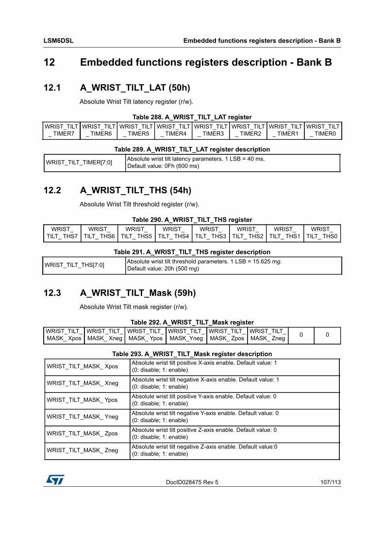
DocID028475 Rev 5 107/113
LSM6DSL Embedded functions registers description - Bank B
113
12 Embedded functions registers description - Bank B
12.1 A_WRIST_TILT_LAT (50h)Absolute Wrist Tilt latency register (r/w).
12.2 A_WRIST_TILT_THS (54h)Absolute Wrist Tilt threshold register (r/w).
12.3 A_WRIST_TILT_Mask (59h)Absolute Wrist Tilt mask register (r/w).
Table 288. A_WRIST_TILT_LAT registerWRIST_TILT
_ TIMER7WRIST_TILT
_ TIMER6WRIST_TILT
_ TIMER5WRIST_TILT
_ TIMER4WRIST_TILT
_ TIMER3WRIST_TILT
_ TIMER2WRIST_TILT
_ TIMER1WRIST_TILT
_ TIMER0
Table 289. A_WRIST_TILT_LAT register description
WRIST_TILT_TIMER[7:0] Absolute wrist tilt latency parameters. 1 LSB = 40 ms. Default value: 0Fh (600 ms)
Table 290. A_WRIST_TILT_THS registerWRIST_
TILT_ THS7WRIST_
TILT_ THS6WRIST_
TILT_ THS5WRIST_
TILT_ THS4WRIST_
TILT_ THS3WRIST_
TILT_ THS2WRIST_
TILT_ THS1WRIST_
TILT_ THS0
Table 291. A_WRIST_TILT_THS register description
WRIST_TILT_THS[7:0] Absolute wrist tilt threshold parameters. 1 LSB = 15.625 mg. Default value: 20h (500 mg)
Table 292. A_WRIST_TILT_Mask registerWRIST_TILT_MASK_ Xpos
WRIST_TILT_MASK_ Xneg
WRIST_TILT_MASK_ Ypos
WRIST_TILT_MASK_Yneg
WRIST_TILT_MASK_ Zpos
WRIST_TILT_MASK_ Zneg 0 0
Table 293. A_WRIST_TILT_Mask register description
WRIST_TILT_MASK_ Xpos Absolute wrist tilt positive X-axis enable. Default value: 1 (0: disable; 1: enable)
WRIST_TILT_MASK_ Xneg Absolute wrist tilt negative X-axis enable. Default value: 1 (0: disable; 1: enable)
WRIST_TILT_MASK_ Ypos Absolute wrist tilt positive Y-axis enable. Default value: 0 (0: disable; 1: enable)
WRIST_TILT_MASK_ Yneg Absolute wrist tilt negative Y-axis enable. Default value: 0 (0: disable; 1: enable)
WRIST_TILT_MASK_ Zpos Absolute wrist tilt positive Z-axis enable. Default value: 0 (0: disable; 1: enable)
WRIST_TILT_MASK_ Zneg Absolute wrist tilt negative Z-axis enable. Default value:0 (0: disable; 1: enable)

Soldering information LSM6DSL
108/113 DocID028475 Rev 5
13 Soldering information
The LGA package is compliant with the ECOPACK®, RoHS and "Green" standard. It is qualified for soldering heat resistance according to JEDEC J-STD-020.
Land pattern and soldering recommendations are available at www.st.com/mems.
DocID028475 Rev 5 109/113
LSM6DSL Package information
113
14 Package information
In order to meet environmental requirements, ST offers these devices in different grades ofECOPACK® packages, depending on their level of environmental compliance. ECOPACK®
specifications, grade definitions and product status are available at: www.st.com. ECOPACK is an ST trademark.
14.1 LGA-14 package information
Figure 17. LGA-14 2.5x3x0.86 mm package outline and mechanical data
Package information LSM6DSL
110/113 DocID028475 Rev 5
14.2 LGA-14 packing information
Figure 18. Carrier tape information for LGA-14 package
Figure 19. LGA-14 package orientation in carrier tape
DocID028475 Rev 5 111/113
LSM6DSL Package information
113
Figure 20. Reel information for carrier tape of LGA-14 package
Table 294. Reel dimensions for carrier tape of LGA-14 packageReel dimensions (mm)
A (max) 330
B (min) 1.5
C 13 ±0.25
D (min) 20.2
N (min) 60
G 12.4 +2/-0
T (max) 18.4
Revision history LSM6DSL
112/113 DocID028475 Rev 5
15 Revision history
Table 295. Document revision history Date Revision Changes
10-Dec-2015 1 Initial release
01-Feb-2016 2
Updated Table 3: Mechanical characteristicsUpdated Table 4: Electrical characteristicsUpdated Figure 7: Accelerometer chain Updated Section 9: Register description
12-Feb-2016 3 Updated Table 3: Mechanical characteristics
29-Jun-2016 4
Document status promoted to production dataUpdated Table 3: Mechanical characteristicsAdded Table 17: Internal pin statusUpdated DRDY_PULSE_CFG_G (0Bh)Updated bit 6 in CTRL4_C (13h)Added WRIST_TILT_EN bit to CTRL10_C (19h)Added FUNC_SRC2 (54h)
28-Oct-2016 5
Updated Features concerning AndroidUpdated Section 2: Embedded low-power featuresAdded Section 2.2: Absolute wrist tiltAdded footnote 14 concerning accelerometer self-test to Table 3Updated Vdd_IO in Section Table 4.: Electrical characteristicsUpdated Figure 8: Accelerometer composite filterUpdated Figure 11 and Figure 13Updated pin 12 (pin status modes) in Table 17: Internal pin statusUpdated FUNC_CFG_ACCESS (01h)Updated CTRL4_C (13h)Updated CTRL6_C (15h)Updated CTRL9_XL (18h)Updated D6D_SRC (1Dh)Added WRIST_TILT_IA (55h)Separated embedded registers into Section 11: Embedded functions registers description - Bank A (02h through 32h) and Section 12: Embedded functions registers description - Bank B (50h through 59h)Updated SLAVE1_CONFIG (07h)Added A_WRIST_TILT_LAT (50h), A_WRIST_TILT_THS (54h), and A_WRIST_TILT_Mask (59h)Minor textual updates

DocID028475 Rev 5 113/113
LSM6DSL
113
IMPORTANT NOTICE – PLEASE READ CAREFULLY
STMicroelectronics NV and its subsidiaries (“ST”) reserve the right to make changes, corrections, enhancements, modifications, and improvements to ST products and/or to this document at any time without notice. Purchasers should obtain the latest relevant information on ST products before placing orders. ST products are sold pursuant to ST’s terms and conditions of sale in place at the time of order acknowledgement.
Purchasers are solely responsible for the choice, selection, and use of ST products and ST assumes no liability for application assistance or the design of Purchasers’ products.
No license, express or implied, to any intellectual property right is granted by ST herein.
Resale of ST products with provisions different from the information set forth herein shall void any warranty granted by ST for such product.
ST and the ST logo are trademarks of ST. All other product or service names are the property of their respective owners.
Information in this document supersedes and replaces information previously supplied in any prior versions of this document.
© 2016 STMicroelectronics – All rights reserved