iNEMO inertial module: 3D accelerometer, 3D gyroscope, 3D ...iNEMO inertial module: 3D...
72
This is information on a product in full production. March 2015 DocID025715 Rev 3 1/72 LSM9DS1 iNEMO inertial module: 3D accelerometer, 3D gyroscope, 3D magnetometer Datasheet - production data Features • 3 acceleration channels, 3 angular rate channels, 3 magnetic field channels • ±2/±4/±8/±16 g linear acceleration full scale • ±4/±8/±12/±16 gauss magnetic full scale • ±245/±500/±2000 dps angular rate full scale • 16-bit data output • SPI / I 2 C serial interfaces • Analog supply voltage 1.9 V to 3.6 V • “Always-on” eco power mode down to 1.9 mA • Programmable interrupt generators • Embedded temperature sensor • Embedded FIFO • Position and motion detection functions • Click/double-click recognition • Intelligent power saving for handheld devices • ECOPACK ® , RoHS and “Green” compliant Applications • Indoor navigation • Smart user interfaces • Advanced gesture recognition • Gaming and virtual reality input devices • Display/map orientation and browsing Description The LSM9DS1 is a system-in-package featuring a 3D digital linear acceleration sensor, a 3D digital angular rate sensor, and a 3D digital magnetic sensor. The LSM9DS1 has a linear acceleration full scale of ±2g/±4g/±8/±16 g, a magnetic field full scale of ±4/±8/±12/±16 gauss and an angular rate of ±245/±500/±2000 dps. The LSM9DS1 includes an I 2 C serial bus interface supporting standard and fast mode (100 kHz and 400 kHz) and an SPI serial standard interface. Magnetic, accelerometer and gyroscope sensing can be enabled or set in power-down mode separately for smart power management. The LSM9DS1 is available in a plastic land grid array package (LGA) and it is guaranteed to operate over an extended temperature range from -40 °C to +85 °C. LGA-24L (3.5x3x1.0 mm) Table 1. Device summary Part number Temperature range [°C] Package Packing LSM9DS1 -40 to +85 LGA-24L Tray LSM9DS1TR -40 to +85 LGA-24L Tape and reel www.st.com
Transcript of iNEMO inertial module: 3D accelerometer, 3D gyroscope, 3D ...iNEMO inertial module: 3D...

This is information on a product in full production.
March 2015 DocID025715 Rev 3 1/72
LSM9DS1
iNEMO inertial module:3D accelerometer, 3D gyroscope, 3D magnetometer
Datasheet - production data
Features
• 3 acceleration channels, 3 angular rate channels, 3 magnetic field channels
• ±2/±4/±8/±16 g linear acceleration full scale
• ±4/±8/±12/±16 gauss magnetic full scale
• ±245/±500/±2000 dps angular rate full scale
• 16-bit data output
• SPI / I2C serial interfaces
• Analog supply voltage 1.9 V to 3.6 V
• “Always-on” eco power mode down to 1.9 mA
• Programmable interrupt generators
• Embedded temperature sensor
• Embedded FIFO
• Position and motion detection functions
• Click/double-click recognition
• Intelligent power saving for handheld devices
• ECOPACK®, RoHS and “Green” compliant
Applications
• Indoor navigation
• Smart user interfaces
• Advanced gesture recognition
• Gaming and virtual reality input devices
• Display/map orientation and browsing
Description
The LSM9DS1 is a system-in-package featuring a 3D digital linear acceleration sensor, a 3D digital angular rate sensor, and a 3D digital magnetic sensor.
The LSM9DS1 has a linear acceleration full scale of ±2g/±4g/±8/±16 g, a magnetic field full scale of ±4/±8/±12/±16 gauss and an angular rate of ±245/±500/±2000 dps.
The LSM9DS1 includes an I2C serial bus interface supporting standard and fast mode (100 kHz and 400 kHz) and an SPI serial standard interface.
Magnetic, accelerometer and gyroscope sensing can be enabled or set in power-down mode separately for smart power management.
The LSM9DS1 is available in a plastic land grid array package (LGA) and it is guaranteed to operate over an extended temperature range from -40 °C to +85 °C.
LGA-24L (3.5x3x1.0 mm)
Table 1. Device summary
Part number Temperature range [°C] Package Packing
LSM9DS1 -40 to +85 LGA-24L Tray
LSM9DS1TR -40 to +85 LGA-24L Tape and reel
www.st.com

Contents LSM9DS1
2/72 DocID025715 Rev 3
Contents
1 Pin description . . . . . . . . . . . . . . . . . . . . . . . . . . . . . . . . . . . . . . . . . . . . 10
2 Module specifications . . . . . . . . . . . . . . . . . . . . . . . . . . . . . . . . . . . . . . . 12
2.1 Sensor characteristics . . . . . . . . . . . . . . . . . . . . . . . . . . . . . . . . . . . . . . . 12
2.2 Electrical characteristics . . . . . . . . . . . . . . . . . . . . . . . . . . . . . . . . . . . . . . 13
2.2.1 Recommended power-up sequence . . . . . . . . . . . . . . . . . . . . . . . . . . . 14
2.3 Temperature sensor characteristics . . . . . . . . . . . . . . . . . . . . . . . . . . . . . 14
2.4 Communication interface characteristics . . . . . . . . . . . . . . . . . . . . . . . . . 15
2.4.1 SPI - serial peripheral interface . . . . . . . . . . . . . . . . . . . . . . . . . . . . . . . 15
2.4.2 I2C - inter-IC control interface . . . . . . . . . . . . . . . . . . . . . . . . . . . . . . . . 16
2.5 Absolute maximum ratings . . . . . . . . . . . . . . . . . . . . . . . . . . . . . . . . . . . . 17
2.6 Terminology . . . . . . . . . . . . . . . . . . . . . . . . . . . . . . . . . . . . . . . . . . . . . . . 18
2.6.1 Sensitivity . . . . . . . . . . . . . . . . . . . . . . . . . . . . . . . . . . . . . . . . . . . . . . . . 18
2.6.2 Zero-g, zero-rate and zero-gauss level . . . . . . . . . . . . . . . . . . . . . . . . . 18
3 LSM9DS1 functionality . . . . . . . . . . . . . . . . . . . . . . . . . . . . . . . . . . . . . . 19
3.1 Operating modes . . . . . . . . . . . . . . . . . . . . . . . . . . . . . . . . . . . . . . . . . . . 19
3.2 Gyroscope power modes . . . . . . . . . . . . . . . . . . . . . . . . . . . . . . . . . . . . . 19
3.3 Accelerometer and gyroscope multiple reads (burst) . . . . . . . . . . . . . . . . 21
3.4 Block diagram . . . . . . . . . . . . . . . . . . . . . . . . . . . . . . . . . . . . . . . . . . . . . . 22
3.5 Accelerometer and gyroscope FIFO . . . . . . . . . . . . . . . . . . . . . . . . . . . . 23
3.5.1 Bypass mode . . . . . . . . . . . . . . . . . . . . . . . . . . . . . . . . . . . . . . . . . . . . . 23
3.5.2 FIFO mode . . . . . . . . . . . . . . . . . . . . . . . . . . . . . . . . . . . . . . . . . . . . . . . 24
3.5.3 Continuous mode . . . . . . . . . . . . . . . . . . . . . . . . . . . . . . . . . . . . . . . . . . 24
3.5.4 Continuous-to-FIFO mode . . . . . . . . . . . . . . . . . . . . . . . . . . . . . . . . . . . 25
3.5.5 Bypass-to-Continuous mode . . . . . . . . . . . . . . . . . . . . . . . . . . . . . . . . . 26
4 Application hints . . . . . . . . . . . . . . . . . . . . . . . . . . . . . . . . . . . . . . . . . . . 27
4.1 External capacitors . . . . . . . . . . . . . . . . . . . . . . . . . . . . . . . . . . . . . . . . . . 27
5 Digital interfaces . . . . . . . . . . . . . . . . . . . . . . . . . . . . . . . . . . . . . . . . . . . 28
5.1 I2C serial interface . . . . . . . . . . . . . . . . . . . . . . . . . . . . . . . . . . . . . . . . . . 28
5.1.1 I2C operation . . . . . . . . . . . . . . . . . . . . . . . . . . . . . . . . . . . . . . . . . . . . . 29

DocID025715 Rev 3 3/72
LSM9DS1 Contents
72
5.2 Accelerometer and gyroscope SPI bus interface . . . . . . . . . . . . . . . . . . . 31
5.2.1 SPI read . . . . . . . . . . . . . . . . . . . . . . . . . . . . . . . . . . . . . . . . . . . . . . . . . 32
5.2.2 SPI write . . . . . . . . . . . . . . . . . . . . . . . . . . . . . . . . . . . . . . . . . . . . . . . . 33
5.2.3 SPI read in 3-wire mode . . . . . . . . . . . . . . . . . . . . . . . . . . . . . . . . . . . . 33
5.3 Magnetic sensor SPI bus interface . . . . . . . . . . . . . . . . . . . . . . . . . . . . . . 34
5.3.1 SPI read . . . . . . . . . . . . . . . . . . . . . . . . . . . . . . . . . . . . . . . . . . . . . . . . . 35
5.3.2 SPI write . . . . . . . . . . . . . . . . . . . . . . . . . . . . . . . . . . . . . . . . . . . . . . . . 36
5.3.3 SPI read in 3-wire mode . . . . . . . . . . . . . . . . . . . . . . . . . . . . . . . . . . . . 37
6 Register mapping . . . . . . . . . . . . . . . . . . . . . . . . . . . . . . . . . . . . . . . . . . 38
7 Accelerometer and gyroscope register description . . . . . . . . . . . . . . 41
7.1 ACT_THS (04h) . . . . . . . . . . . . . . . . . . . . . . . . . . . . . . . . . . . . . . . . . . . . 41
7.2 ACT_DUR (05h) . . . . . . . . . . . . . . . . . . . . . . . . . . . . . . . . . . . . . . . . . . . . 41
7.3 INT_GEN_CFG_XL (06h) . . . . . . . . . . . . . . . . . . . . . . . . . . . . . . . . . . . . 41
7.4 INT_GEN_THS_X_XL (07h) . . . . . . . . . . . . . . . . . . . . . . . . . . . . . . . . . . 42
7.5 INT_GEN_THS_Y_XL (08h) . . . . . . . . . . . . . . . . . . . . . . . . . . . . . . . . . . 42
7.6 INT_GEN_THS_Z_XL (09h) . . . . . . . . . . . . . . . . . . . . . . . . . . . . . . . . . . . 43
7.7 INT_GEN_DUR_XL (0Ah) . . . . . . . . . . . . . . . . . . . . . . . . . . . . . . . . . . . . 43
7.8 REFERENCE_G (0Bh) . . . . . . . . . . . . . . . . . . . . . . . . . . . . . . . . . . . . . . . 43
7.9 INT1_CTRL (0Ch) . . . . . . . . . . . . . . . . . . . . . . . . . . . . . . . . . . . . . . . . . . 43
7.10 INT2_CTRL (0Dh) . . . . . . . . . . . . . . . . . . . . . . . . . . . . . . . . . . . . . . . . . . 44
7.11 WHO_AM_I (0Fh) . . . . . . . . . . . . . . . . . . . . . . . . . . . . . . . . . . . . . . . . . . . 45
7.12 CTRL_REG1_G (10h) . . . . . . . . . . . . . . . . . . . . . . . . . . . . . . . . . . . . . . . 45
7.13 CTRL_REG2_G (11h) . . . . . . . . . . . . . . . . . . . . . . . . . . . . . . . . . . . . . . . 47
7.14 CTRL_REG3_G (12h) . . . . . . . . . . . . . . . . . . . . . . . . . . . . . . . . . . . . . . . 47
7.15 ORIENT_CFG_G (13h) . . . . . . . . . . . . . . . . . . . . . . . . . . . . . . . . . . . . . . 48
7.16 INT_GEN_SRC_G (14h) . . . . . . . . . . . . . . . . . . . . . . . . . . . . . . . . . . . . . 48
7.17 OUT_TEMP_L (15h), OUT_TEMP_H (16h) . . . . . . . . . . . . . . . . . . . . . . . 49
7.18 STATUS_REG (17h) . . . . . . . . . . . . . . . . . . . . . . . . . . . . . . . . . . . . . . . . 49
7.19 OUT_X_G (18h - 19h) . . . . . . . . . . . . . . . . . . . . . . . . . . . . . . . . . . . . . . . 50
7.20 OUT_Y_G (1Ah - 1Bh) . . . . . . . . . . . . . . . . . . . . . . . . . . . . . . . . . . . . . . . 50
7.21 OUT_Z_G (1Ch - 1Dh) . . . . . . . . . . . . . . . . . . . . . . . . . . . . . . . . . . . . . . . 50
7.22 CTRL_REG4 (1Eh) . . . . . . . . . . . . . . . . . . . . . . . . . . . . . . . . . . . . . . . . . 50

Contents LSM9DS1
4/72 DocID025715 Rev 3
7.23 CTRL_REG5_XL (1Fh) . . . . . . . . . . . . . . . . . . . . . . . . . . . . . . . . . . . . . . 51
7.24 CTRL_REG6_XL (20h) . . . . . . . . . . . . . . . . . . . . . . . . . . . . . . . . . . . . . . 51
7.25 CTRL_REG7_XL (21h) . . . . . . . . . . . . . . . . . . . . . . . . . . . . . . . . . . . . . . 52
7.26 CTRL_REG8 (22h) . . . . . . . . . . . . . . . . . . . . . . . . . . . . . . . . . . . . . . . . . . 53
7.27 CTRL_REG9 (23h) . . . . . . . . . . . . . . . . . . . . . . . . . . . . . . . . . . . . . . . . . . 54
7.28 CTRL_REG10 (24h) . . . . . . . . . . . . . . . . . . . . . . . . . . . . . . . . . . . . . . . . . 54
7.29 INT_GEN_SRC_XL (26h) . . . . . . . . . . . . . . . . . . . . . . . . . . . . . . . . . . . . 54
7.30 STATUS_REG (27h) . . . . . . . . . . . . . . . . . . . . . . . . . . . . . . . . . . . . . . . . 55
7.31 OUT_X_XL (28h - 29h) . . . . . . . . . . . . . . . . . . . . . . . . . . . . . . . . . . . . . . 56
7.32 OUT_Y_XL (2Ah - 2Bh) . . . . . . . . . . . . . . . . . . . . . . . . . . . . . . . . . . . . . . 56
7.33 OUT_Z_XL (2Ch - 2Dh) . . . . . . . . . . . . . . . . . . . . . . . . . . . . . . . . . . . . . . 56
7.34 FIFO_CTRL (2Eh) . . . . . . . . . . . . . . . . . . . . . . . . . . . . . . . . . . . . . . . . . . 56
7.35 FIFO_SRC (2Fh) . . . . . . . . . . . . . . . . . . . . . . . . . . . . . . . . . . . . . . . . . . . 57
7.36 INT_GEN_CFG_G (30h) . . . . . . . . . . . . . . . . . . . . . . . . . . . . . . . . . . . . . 57
7.37 INT_GEN_THS_X_G (31h - 32h) . . . . . . . . . . . . . . . . . . . . . . . . . . . . . . . 58
7.38 INT_GEN_THS_Y_G (33h - 34h) . . . . . . . . . . . . . . . . . . . . . . . . . . . . . . . 59
7.39 INT_GEN_THS_Z_G (35h - 36h) . . . . . . . . . . . . . . . . . . . . . . . . . . . . . . . 59
7.40 INT_GEN_DUR_G (37h) . . . . . . . . . . . . . . . . . . . . . . . . . . . . . . . . . . . . . 59
8 Magnetometer register description . . . . . . . . . . . . . . . . . . . . . . . . . . . . 62
8.1 OFFSET_X_REG_L_M (05h), OFFSET_X_REG_H_M (06h) . . . . . . . . . 62
8.2 OFFSET_Y_REG_L_M (07h), OFFSET_Y_REG_H_M (08h) . . . . . . . . . 62
8.3 OFFSET_Z_REG_L_M (09h), OFFSET_Z_REG_H_M (0Ah) . . . . . . . . . 62
8.4 WHO_AM_I_M (0Fh) . . . . . . . . . . . . . . . . . . . . . . . . . . . . . . . . . . . . . . . . 63
8.5 CTRL_REG1_M (20h) . . . . . . . . . . . . . . . . . . . . . . . . . . . . . . . . . . . . . . . 63
8.6 CTRL_REG2_M (21h) . . . . . . . . . . . . . . . . . . . . . . . . . . . . . . . . . . . . . . . 64
8.7 CTRL_REG3_M (22h) . . . . . . . . . . . . . . . . . . . . . . . . . . . . . . . . . . . . . . . 64
8.8 CTRL_REG4_M (23h) . . . . . . . . . . . . . . . . . . . . . . . . . . . . . . . . . . . . . . . 65
8.9 CTRL_REG5_M (24h) . . . . . . . . . . . . . . . . . . . . . . . . . . . . . . . . . . . . . . . 65
8.10 STATUS_REG_M (27h) . . . . . . . . . . . . . . . . . . . . . . . . . . . . . . . . . . . . . . 66
8.11 OUT_X_L_M (28h), OUT_X_H_M(29h) . . . . . . . . . . . . . . . . . . . . . . . . . . 66
8.12 OUT_Y_L_M (2Ah), OUT_Y_H_M (2Bh) . . . . . . . . . . . . . . . . . . . . . . . . . 66
8.13 OUT_Z_L_M (2Ch), OUT_Z_H_M (2Dh) . . . . . . . . . . . . . . . . . . . . . . . . . 66

DocID025715 Rev 3 5/72
LSM9DS1 Contents
72
8.14 INT_CFG_M (30h) . . . . . . . . . . . . . . . . . . . . . . . . . . . . . . . . . . . . . . . . . . 67
8.15 INT_SRC_M (31h) . . . . . . . . . . . . . . . . . . . . . . . . . . . . . . . . . . . . . . . . . . 67
8.16 INT_THS_L(32h), INT_THS_H(33h) . . . . . . . . . . . . . . . . . . . . . . . . . . . . 68
9 Package information . . . . . . . . . . . . . . . . . . . . . . . . . . . . . . . . . . . . . . . . 69
9.1 Soldering information . . . . . . . . . . . . . . . . . . . . . . . . . . . . . . . . . . . . . . . . 69
9.2 LGA package information . . . . . . . . . . . . . . . . . . . . . . . . . . . . . . . . . . . . . 69
10 Revision history . . . . . . . . . . . . . . . . . . . . . . . . . . . . . . . . . . . . . . . . . . . 71

List of tables LSM9DS1
6/72 DocID025715 Rev 3
List of tables
Table 1. Device summary . . . . . . . . . . . . . . . . . . . . . . . . . . . . . . . . . . . . . . . . . . . . . . . . . . . . . . . . . . 1Table 2. Pin description . . . . . . . . . . . . . . . . . . . . . . . . . . . . . . . . . . . . . . . . . . . . . . . . . . . . . . . . . . 11Table 3. Sensor characteristics . . . . . . . . . . . . . . . . . . . . . . . . . . . . . . . . . . . . . . . . . . . . . . . . . . . . 12Table 4. Electrical characteristics . . . . . . . . . . . . . . . . . . . . . . . . . . . . . . . . . . . . . . . . . . . . . . . . . . . 13Table 5. Temperature sensor characteristics . . . . . . . . . . . . . . . . . . . . . . . . . . . . . . . . . . . . . . . . . . 14Table 6. SPI slave timing values. . . . . . . . . . . . . . . . . . . . . . . . . . . . . . . . . . . . . . . . . . . . . . . . . . . . 15Table 7. I2C slave timing values . . . . . . . . . . . . . . . . . . . . . . . . . . . . . . . . . . . . . . . . . . . . . . . . . . . . 16Table 8. Absolute maximum ratings . . . . . . . . . . . . . . . . . . . . . . . . . . . . . . . . . . . . . . . . . . . . . . . . . 17Table 9. Gyroscope operating modes. . . . . . . . . . . . . . . . . . . . . . . . . . . . . . . . . . . . . . . . . . . . . . . . 20Table 10. Operating mode current consumption . . . . . . . . . . . . . . . . . . . . . . . . . . . . . . . . . . . . . . . . 20Table 11. Accelerometer turn-on time . . . . . . . . . . . . . . . . . . . . . . . . . . . . . . . . . . . . . . . . . . . . . . . . 20Table 12. Gyroscope turn-on time . . . . . . . . . . . . . . . . . . . . . . . . . . . . . . . . . . . . . . . . . . . . . . . . . . . 21Table 13. Serial interface pin description . . . . . . . . . . . . . . . . . . . . . . . . . . . . . . . . . . . . . . . . . . . . . . 28Table 14. I2C terminology . . . . . . . . . . . . . . . . . . . . . . . . . . . . . . . . . . . . . . . . . . . . . . . . . . . . . . . . . . 28Table 15. Transfer when master is writing one byte to slave . . . . . . . . . . . . . . . . . . . . . . . . . . . . . . . 29Table 16. Transfer when master is writing multiple bytes to slave . . . . . . . . . . . . . . . . . . . . . . . . . . . 29Table 17. Transfer when master is receiving (reading) one byte of data from slave . . . . . . . . . . . . . 29Table 18. Transfer when master is receiving (reading) multiple bytes of data from slave . . . . . . . . . 29Table 19. Accelerometer and gyroscope SAD+Read/Write patterns . . . . . . . . . . . . . . . . . . . . . . . . . 30Table 20. Magnetic sensor SAD+Read/Write patterns . . . . . . . . . . . . . . . . . . . . . . . . . . . . . . . . . . . . 30Table 21. Accelerometer and gyroscope register address map . . . . . . . . . . . . . . . . . . . . . . . . . . . . . 38Table 22. Magnetic sensor register address map. . . . . . . . . . . . . . . . . . . . . . . . . . . . . . . . . . . . . . . . 40Table 23. ACT_THS register . . . . . . . . . . . . . . . . . . . . . . . . . . . . . . . . . . . . . . . . . . . . . . . . . . . . . . . 41Table 24. ACT_THS register description . . . . . . . . . . . . . . . . . . . . . . . . . . . . . . . . . . . . . . . . . . . . . . 41Table 25. ACT_DUR register . . . . . . . . . . . . . . . . . . . . . . . . . . . . . . . . . . . . . . . . . . . . . . . . . . . . . . . 41Table 26. ACT_DUR register description . . . . . . . . . . . . . . . . . . . . . . . . . . . . . . . . . . . . . . . . . . . . . . 41Table 27. INT_GEN_CFG_XL register . . . . . . . . . . . . . . . . . . . . . . . . . . . . . . . . . . . . . . . . . . . . . . . . 41Table 28. INT_GEN_CFG_XL register description . . . . . . . . . . . . . . . . . . . . . . . . . . . . . . . . . . . . . . . 42Table 29. INT_GEN_THS_X_XL register . . . . . . . . . . . . . . . . . . . . . . . . . . . . . . . . . . . . . . . . . . . . . . 42Table 30. INT_GEN_THS_X_XL register description . . . . . . . . . . . . . . . . . . . . . . . . . . . . . . . . . . . . . 42Table 31. INT_GEN_THS_Y_XL register . . . . . . . . . . . . . . . . . . . . . . . . . . . . . . . . . . . . . . . . . . . . . . 42Table 32. INT_GEN_THS_Y_XL register description . . . . . . . . . . . . . . . . . . . . . . . . . . . . . . . . . . . . . 42Table 33. INT_GEN_THS_Z_XL register . . . . . . . . . . . . . . . . . . . . . . . . . . . . . . . . . . . . . . . . . . . . . . 43Table 34. INT_GEN_THS_Z_XL register description . . . . . . . . . . . . . . . . . . . . . . . . . . . . . . . . . . . . . 43Table 35. INT_GEN_DUR_XL register . . . . . . . . . . . . . . . . . . . . . . . . . . . . . . . . . . . . . . . . . . . . . . . . 43Table 36. INT_GEN_DUR_XL register description. . . . . . . . . . . . . . . . . . . . . . . . . . . . . . . . . . . . . . . 43Table 37. REFERENCE_G register . . . . . . . . . . . . . . . . . . . . . . . . . . . . . . . . . . . . . . . . . . . . . . . . . . 43Table 38. REFERENCE_G register description . . . . . . . . . . . . . . . . . . . . . . . . . . . . . . . . . . . . . . . . . 43Table 39. INT1_CTRL register . . . . . . . . . . . . . . . . . . . . . . . . . . . . . . . . . . . . . . . . . . . . . . . . . . . . . . 43Table 40. INT1_CTRL register description . . . . . . . . . . . . . . . . . . . . . . . . . . . . . . . . . . . . . . . . . . . . . 44Table 41. INT2_CTRL register . . . . . . . . . . . . . . . . . . . . . . . . . . . . . . . . . . . . . . . . . . . . . . . . . . . . . . 44Table 42. INT2_CTRL register description . . . . . . . . . . . . . . . . . . . . . . . . . . . . . . . . . . . . . . . . . . . . . 44Table 43. WHO_AM_I register . . . . . . . . . . . . . . . . . . . . . . . . . . . . . . . . . . . . . . . . . . . . . . . . . . . . . . 45Table 44. CTRL_REG1_G register . . . . . . . . . . . . . . . . . . . . . . . . . . . . . . . . . . . . . . . . . . . . . . . . . . . 45Table 45. CTRL_REG1_G register description . . . . . . . . . . . . . . . . . . . . . . . . . . . . . . . . . . . . . . . . . 45Table 46. ODR and BW configuration setting (after LPF1). . . . . . . . . . . . . . . . . . . . . . . . . . . . . . . . . 45Table 47. ODR and BW configuration setting (after LPF2). . . . . . . . . . . . . . . . . . . . . . . . . . . . . . . . . 46Table 48. CTRL_REG2_G register . . . . . . . . . . . . . . . . . . . . . . . . . . . . . . . . . . . . . . . . . . . . . . . . . . . 47

DocID025715 Rev 3 7/72
LSM9DS1 List of tables
72
Table 49. CTRL_REG2_G register description . . . . . . . . . . . . . . . . . . . . . . . . . . . . . . . . . . . . . . . . . 47Table 50. CTRL_REG3_G register . . . . . . . . . . . . . . . . . . . . . . . . . . . . . . . . . . . . . . . . . . . . . . . . . . . 47Table 51. CTRL_REG3_G register description . . . . . . . . . . . . . . . . . . . . . . . . . . . . . . . . . . . . . . . . . 47Table 52. Gyroscope high-pass filter cutoff frequency configuration [Hz]. . . . . . . . . . . . . . . . . . . . . . 48Table 53. ORIENT_CFG_G register . . . . . . . . . . . . . . . . . . . . . . . . . . . . . . . . . . . . . . . . . . . . . . . . . . 48Table 54. ORIENT_CFG_G register description . . . . . . . . . . . . . . . . . . . . . . . . . . . . . . . . . . . . . . . . 48Table 55. INT_GEN_SRC_G register . . . . . . . . . . . . . . . . . . . . . . . . . . . . . . . . . . . . . . . . . . . . . . . . . 48Table 56. INT_GEN_SRC_G register description . . . . . . . . . . . . . . . . . . . . . . . . . . . . . . . . . . . . . . . 49Table 57. OUT_TEMP_L register . . . . . . . . . . . . . . . . . . . . . . . . . . . . . . . . . . . . . . . . . . . . . . . . . . . . 49Table 58. OUT_TEMP_H register. . . . . . . . . . . . . . . . . . . . . . . . . . . . . . . . . . . . . . . . . . . . . . . . . . . . 49Table 59. OUT_TEMP register description. . . . . . . . . . . . . . . . . . . . . . . . . . . . . . . . . . . . . . . . . . . . . 49Table 60. STATUS_REG register . . . . . . . . . . . . . . . . . . . . . . . . . . . . . . . . . . . . . . . . . . . . . . . . . . . . 49Table 61. STATUS_REG register description . . . . . . . . . . . . . . . . . . . . . . . . . . . . . . . . . . . . . . . . . . 50Table 62. CTRL_REG4 register . . . . . . . . . . . . . . . . . . . . . . . . . . . . . . . . . . . . . . . . . . . . . . . . . . . . . 50Table 63. CTRL_REG4 register description . . . . . . . . . . . . . . . . . . . . . . . . . . . . . . . . . . . . . . . . . . . . 51Table 64. CTRL_REG5_XL register . . . . . . . . . . . . . . . . . . . . . . . . . . . . . . . . . . . . . . . . . . . . . . . . . . 51Table 65. CTRL_REG5_XL register description. . . . . . . . . . . . . . . . . . . . . . . . . . . . . . . . . . . . . . . . . 51Table 66. CTRL_REG6_XL register . . . . . . . . . . . . . . . . . . . . . . . . . . . . . . . . . . . . . . . . . . . . . . . . . . 51Table 67. CTRL_REG6_XL register description. . . . . . . . . . . . . . . . . . . . . . . . . . . . . . . . . . . . . . . . . 52Table 68. ODR register setting (accelerometer only mode) . . . . . . . . . . . . . . . . . . . . . . . . . . . . . . . . 52Table 69. CTRL_REG7_XL register . . . . . . . . . . . . . . . . . . . . . . . . . . . . . . . . . . . . . . . . . . . . . . . . . . 52Table 70. CTRL_REG7_XL register description. . . . . . . . . . . . . . . . . . . . . . . . . . . . . . . . . . . . . . . . . 53Table 71. Low pass cutoff frequency in high resolution mode (HR = 1) . . . . . . . . . . . . . . . . . . . . . . . 53Table 72. CTRL_REG8 register . . . . . . . . . . . . . . . . . . . . . . . . . . . . . . . . . . . . . . . . . . . . . . . . . . . . . 53Table 73. CTRL_REG8 register description . . . . . . . . . . . . . . . . . . . . . . . . . . . . . . . . . . . . . . . . . . . . 53Table 74. CTRL_REG9 register . . . . . . . . . . . . . . . . . . . . . . . . . . . . . . . . . . . . . . . . . . . . . . . . . . . . . 54Table 75. CTRL_REG9 register description . . . . . . . . . . . . . . . . . . . . . . . . . . . . . . . . . . . . . . . . . . . . 54Table 76. CTRL_REG10 register . . . . . . . . . . . . . . . . . . . . . . . . . . . . . . . . . . . . . . . . . . . . . . . . . . . . 54Table 77. CTRL_REG10 register description . . . . . . . . . . . . . . . . . . . . . . . . . . . . . . . . . . . . . . . . . . . 54Table 78. INT_GEN_SRC_XL register . . . . . . . . . . . . . . . . . . . . . . . . . . . . . . . . . . . . . . . . . . . . . . . . 54Table 79. INT_GEN_SRC_XL register description . . . . . . . . . . . . . . . . . . . . . . . . . . . . . . . . . . . . . . . 55Table 80. STATUS_REG register . . . . . . . . . . . . . . . . . . . . . . . . . . . . . . . . . . . . . . . . . . . . . . . . . . . . 55Table 81. STATUS_REG register description . . . . . . . . . . . . . . . . . . . . . . . . . . . . . . . . . . . . . . . . . . 55Table 82. FIFO_CTRL register . . . . . . . . . . . . . . . . . . . . . . . . . . . . . . . . . . . . . . . . . . . . . . . . . . . . . 56Table 83. FIFO_CTRL register description. . . . . . . . . . . . . . . . . . . . . . . . . . . . . . . . . . . . . . . . . . . . . 56Table 84. FIFO mode selection . . . . . . . . . . . . . . . . . . . . . . . . . . . . . . . . . . . . . . . . . . . . . . . . . . . . . 56Table 85. FIFO_SRC register . . . . . . . . . . . . . . . . . . . . . . . . . . . . . . . . . . . . . . . . . . . . . . . . . . . . . . 57Table 86. FIFO_SRC register description. . . . . . . . . . . . . . . . . . . . . . . . . . . . . . . . . . . . . . . . . . . . . . 57Table 87. FIFO_SRC example: OVR/FSS details . . . . . . . . . . . . . . . . . . . . . . . . . . . . . . . . . . . . . . . 57Table 88. INT_GEN_CFG_G register . . . . . . . . . . . . . . . . . . . . . . . . . . . . . . . . . . . . . . . . . . . . . . . . . 57Table 89. INT_GEN_CFG_G register description . . . . . . . . . . . . . . . . . . . . . . . . . . . . . . . . . . . . . . . 58Table 90. INT_GEN_THS_XH_G register . . . . . . . . . . . . . . . . . . . . . . . . . . . . . . . . . . . . . . . . . . . . . 58Table 91. INT_GEN_THS_XL_G register . . . . . . . . . . . . . . . . . . . . . . . . . . . . . . . . . . . . . . . . . . . . . . 58Table 92. INT_GEN_THS_X_G register description . . . . . . . . . . . . . . . . . . . . . . . . . . . . . . . . . . . . . 58Table 93. INT_GEN_THS_YH_G register . . . . . . . . . . . . . . . . . . . . . . . . . . . . . . . . . . . . . . . . . . . . . 59Table 94. INT_GEN_THS_YL_G register . . . . . . . . . . . . . . . . . . . . . . . . . . . . . . . . . . . . . . . . . . . . . . 59Table 95. INT_GEN_THS_Y_G register description . . . . . . . . . . . . . . . . . . . . . . . . . . . . . . . . . . . . . 59Table 96. INT_GEN_THS_ZH_G register . . . . . . . . . . . . . . . . . . . . . . . . . . . . . . . . . . . . . . . . . . . . . 59Table 97. INT_GEN_THS_ZL_G register . . . . . . . . . . . . . . . . . . . . . . . . . . . . . . . . . . . . . . . . . . . . . . 59Table 98. INT_GEN_THS_Z_G register description. . . . . . . . . . . . . . . . . . . . . . . . . . . . . . . . . . . . . . 59Table 99. INT_GEN_DUR_G register. . . . . . . . . . . . . . . . . . . . . . . . . . . . . . . . . . . . . . . . . . . . . . . . . 59Table 100. INT_GEN_DUR_G register description . . . . . . . . . . . . . . . . . . . . . . . . . . . . . . . . . . . . . . . 60

List of tables LSM9DS1
8/72 DocID025715 Rev 3
Table 101. OFFSET_X_REG_L_M register . . . . . . . . . . . . . . . . . . . . . . . . . . . . . . . . . . . . . . . . . . . . . 62Table 102. OFFSET_X_REG_H_M register . . . . . . . . . . . . . . . . . . . . . . . . . . . . . . . . . . . . . . . . . . . . . 62Table 103. OFFSET_Y_REG_L_M register . . . . . . . . . . . . . . . . . . . . . . . . . . . . . . . . . . . . . . . . . . . . . 62Table 104. OFFSET_Y_REG_H_M register . . . . . . . . . . . . . . . . . . . . . . . . . . . . . . . . . . . . . . . . . . . . . 62Table 105. OFFSET_Z_REG_L_M register . . . . . . . . . . . . . . . . . . . . . . . . . . . . . . . . . . . . . . . . . . . . . 62Table 106. OFFSET_Z_REG_H_M register . . . . . . . . . . . . . . . . . . . . . . . . . . . . . . . . . . . . . . . . . . . . . 62Table 107. WHO_AM_I_M register. . . . . . . . . . . . . . . . . . . . . . . . . . . . . . . . . . . . . . . . . . . . . . . . . . . . 63Table 108. CTRL_REG1_M register. . . . . . . . . . . . . . . . . . . . . . . . . . . . . . . . . . . . . . . . . . . . . . . . . . . 63Table 109. CTRL_REG1_M register description . . . . . . . . . . . . . . . . . . . . . . . . . . . . . . . . . . . . . . . . . 63Table 110. X and Y axes operative mode selection . . . . . . . . . . . . . . . . . . . . . . . . . . . . . . . . . . . . . . . 63Table 111. Output data rate configuration . . . . . . . . . . . . . . . . . . . . . . . . . . . . . . . . . . . . . . . . . . . . . . 63Table 112. CTRL_REG2_M register. . . . . . . . . . . . . . . . . . . . . . . . . . . . . . . . . . . . . . . . . . . . . . . . . . . 64Table 113. CTRL_REG2_M register description . . . . . . . . . . . . . . . . . . . . . . . . . . . . . . . . . . . . . . . . . 64Table 114. Full-scale selection . . . . . . . . . . . . . . . . . . . . . . . . . . . . . . . . . . . . . . . . . . . . . . . . . . . . . . . 64Table 115. CTRL_REG3_M register. . . . . . . . . . . . . . . . . . . . . . . . . . . . . . . . . . . . . . . . . . . . . . . . . . . 64Table 116. CTRL_REG3_M register description . . . . . . . . . . . . . . . . . . . . . . . . . . . . . . . . . . . . . . . . . 64Table 117. System operating mode selection. . . . . . . . . . . . . . . . . . . . . . . . . . . . . . . . . . . . . . . . . . . . 65Table 118. CTRL_REG4_M register. . . . . . . . . . . . . . . . . . . . . . . . . . . . . . . . . . . . . . . . . . . . . . . . . . . 65Table 119. CTRL_REG4_M register description . . . . . . . . . . . . . . . . . . . . . . . . . . . . . . . . . . . . . . . . . 65Table 120. Z-axis operative mode selection . . . . . . . . . . . . . . . . . . . . . . . . . . . . . . . . . . . . . . . . . . . . . 65Table 121. CTRL_REG5_M register. . . . . . . . . . . . . . . . . . . . . . . . . . . . . . . . . . . . . . . . . . . . . . . . . . . 65Table 122. CTRL_REG5_M register description . . . . . . . . . . . . . . . . . . . . . . . . . . . . . . . . . . . . . . . . . 65Table 123. STATUS_REG_M register . . . . . . . . . . . . . . . . . . . . . . . . . . . . . . . . . . . . . . . . . . . . . . . . . 66Table 124. STATUS_REG_M register description . . . . . . . . . . . . . . . . . . . . . . . . . . . . . . . . . . . . . . . . 66Table 125. INT_CFG_M register . . . . . . . . . . . . . . . . . . . . . . . . . . . . . . . . . . . . . . . . . . . . . . . . . . . . . 67Table 126. INT_CFG_M register description . . . . . . . . . . . . . . . . . . . . . . . . . . . . . . . . . . . . . . . . . . . . 67Table 127. INT_SRC_M register . . . . . . . . . . . . . . . . . . . . . . . . . . . . . . . . . . . . . . . . . . . . . . . . . . . . . 67Table 128. INT_SRC_M register description . . . . . . . . . . . . . . . . . . . . . . . . . . . . . . . . . . . . . . . . . . . . 67Table 129. INT_THS_L_M register . . . . . . . . . . . . . . . . . . . . . . . . . . . . . . . . . . . . . . . . . . . . . . . . . . . . 68Table 130. INT_THS_H_M register . . . . . . . . . . . . . . . . . . . . . . . . . . . . . . . . . . . . . . . . . . . . . . . . . . . 68Table 131. LGA (3.5x3x1 mm) 24-lead package mechanical data . . . . . . . . . . . . . . . . . . . . . . . . . . . . 70Table 132. Document revision history . . . . . . . . . . . . . . . . . . . . . . . . . . . . . . . . . . . . . . . . . . . . . . . . . 71

DocID025715 Rev 3 9/72
LSM9DS1 List of figures
72
List of figures
Figure 1. Pin connections . . . . . . . . . . . . . . . . . . . . . . . . . . . . . . . . . . . . . . . . . . . . . . . . . . . . . . . . . 10Figure 2. Recommended power-up sequence. . . . . . . . . . . . . . . . . . . . . . . . . . . . . . . . . . . . . . . . . . 14Figure 3. SPI slave timing diagram . . . . . . . . . . . . . . . . . . . . . . . . . . . . . . . . . . . . . . . . . . . . . . . . . . 15Figure 4. I2C slave timing diagram . . . . . . . . . . . . . . . . . . . . . . . . . . . . . . . . . . . . . . . . . . . . . . . . . . 16Figure 5. Switching operating modes. . . . . . . . . . . . . . . . . . . . . . . . . . . . . . . . . . . . . . . . . . . . . . . . . 19Figure 6. Multiple reads: accelerometer only . . . . . . . . . . . . . . . . . . . . . . . . . . . . . . . . . . . . . . . . . . . 21Figure 7. Multiple reads: accelerometer and gyroscope . . . . . . . . . . . . . . . . . . . . . . . . . . . . . . . . . . 21Figure 8. Accelerometer and gyroscope digital block diagram . . . . . . . . . . . . . . . . . . . . . . . . . . . . . 22Figure 9. Magnetometer block diagram . . . . . . . . . . . . . . . . . . . . . . . . . . . . . . . . . . . . . . . . . . . . . . . 22Figure 10. Bypass mode . . . . . . . . . . . . . . . . . . . . . . . . . . . . . . . . . . . . . . . . . . . . . . . . . . . . . . . . . . . 23Figure 11. FIFO mode . . . . . . . . . . . . . . . . . . . . . . . . . . . . . . . . . . . . . . . . . . . . . . . . . . . . . . . . . . . . . 24Figure 12. Continuous mode . . . . . . . . . . . . . . . . . . . . . . . . . . . . . . . . . . . . . . . . . . . . . . . . . . . . . . . . 25Figure 13. Continuous-to-FIFO mode . . . . . . . . . . . . . . . . . . . . . . . . . . . . . . . . . . . . . . . . . . . . . . . . . 25Figure 14. Bypass-to-Continuous mode . . . . . . . . . . . . . . . . . . . . . . . . . . . . . . . . . . . . . . . . . . . . . . . 26Figure 15. LSM9DS1 electrical connections . . . . . . . . . . . . . . . . . . . . . . . . . . . . . . . . . . . . . . . . . . . . 27Figure 16. Accelerometer and gyroscope read and write protocol . . . . . . . . . . . . . . . . . . . . . . . . . . . 31Figure 17. Accelerometer and gyroscope SPI read protocol . . . . . . . . . . . . . . . . . . . . . . . . . . . . . . . . 32Figure 18. Multiple byte SPI read protocol (2-byte example) . . . . . . . . . . . . . . . . . . . . . . . . . . . . . . . . 32Figure 19. Accelerometer and gyroscope SPI write protocol . . . . . . . . . . . . . . . . . . . . . . . . . . . . . . . . 33Figure 20. Multiple byte SPI write protocol (2-byte example). . . . . . . . . . . . . . . . . . . . . . . . . . . . . . . . 33Figure 21. Accelerometer and gyroscope SPI read protocol in 3-wire mode. . . . . . . . . . . . . . . . . . . . 33Figure 22. Magnetic sensor read and write protocol . . . . . . . . . . . . . . . . . . . . . . . . . . . . . . . . . . . . . . 34Figure 23. Magnetic sensor SPI read protocol. . . . . . . . . . . . . . . . . . . . . . . . . . . . . . . . . . . . . . . . . . . 35Figure 24. Multiple byte SPI read protocol (2-byte example) . . . . . . . . . . . . . . . . . . . . . . . . . . . . . . . . 35Figure 25. Magnetic sensor SPI write protocol . . . . . . . . . . . . . . . . . . . . . . . . . . . . . . . . . . . . . . . . . . 36Figure 26. Multiple byte SPI write protocol (2-byte example). . . . . . . . . . . . . . . . . . . . . . . . . . . . . . . . 36Figure 27. SPI read protocol in 3-wire mode . . . . . . . . . . . . . . . . . . . . . . . . . . . . . . . . . . . . . . . . . . . . 37Figure 28. INT_SEL and OUT_SEL configuration gyroscope block diagram . . . . . . . . . . . . . . . . . . . 47Figure 29. Wait bit disabled . . . . . . . . . . . . . . . . . . . . . . . . . . . . . . . . . . . . . . . . . . . . . . . . . . . . . . . . . 60Figure 30. Wait bit enabled . . . . . . . . . . . . . . . . . . . . . . . . . . . . . . . . . . . . . . . . . . . . . . . . . . . . . . . . . 61Figure 31. LGA (3.5x3x1 mm) 24-lead package outline . . . . . . . . . . . . . . . . . . . . . . . . . . . . . . . . . . . 69

Pin description LSM9DS1
10/72 DocID025715 Rev 3
1 Pin description
Figure 1. Pin connections

DocID025715 Rev 3 11/72
LSM9DS1 Pin description
72
Table 2. Pin description
Pin # Name Function
1 VDDIO(1)
1. Recommended 100 nF filter capacitor.
Power supply for I/O pins
2 SCL/SPC I2C serial clock (SCL) / SPI serial port clock (SPC)
3 VDDIO(2)
2. Recommended 100 nF filter capacitor.
Power supply for I/O pins
4 SDA/SDI/SDO
I2C serial data (SDA)
SPI serial data input (SDI)
3-wire interface serial data output (SDO)
5 SDO_A/GSPI serial data output (SDO) for the accelerometer and gyroscope
I2C least significant bit of the device address (SA0) for the accelerometer and gyroscope
6 SDO_MSPI serial data output (SDO) for the magnetometer
I2C least significant bit of the device address (SA0) for the magnetometer
7 CS_A/G
SPI enable
I2C/SPI mode selection for the accelerometer and gyroscope (1: SPI idle mode / I2C communication enabled; 0: SPI communication mode / I2C disabled)
8 CS_M
SPI enable
I2C/SPI mode selection for the magnetometer (1: SPI idle mode / I2C communication enabled; 0: SPI communication mode / I2C disabled)
9 DRDY_M Magnetic sensor data ready
10 INT_M Magnetic sensor interrupt
11 INT1_A/G Accelerometer and gyroscope interrupt 1
12 INT2_A/G Accelerometer and gyroscope interrupt 2
13 DEN_A/G Accelerometer and gyroscope data enable
14 RES Reserved. Connected to GND.
15 RES Reserved. Connected to GND.
16 RES Reserved. Connected to GND.
17 RES Reserved. Connected to GND.
18 RES Reserved. Connected to GND.
19 GND 0 V supply
20 GND 0 V supply
21 CAP Connected to GND with ceramic capacitor(3)
3. 10 nF (±10%), 16 V. 1 nF minimum value has to be guaranteed under 11 V bias condition.
22 VDD(4)
4. Recommended 100 nF plus 10 µF capacitors.
Power supply
23 VDD(5)
5. Recommended 100 nF plus 10 µF capacitors.
Power supply
24 C1 Capacitor connection (C1 = 100 nF)

Module specifications LSM9DS1
12/72 DocID025715 Rev 3
2 Module specifications
2.1 Sensor characteristics
@ Vdd = 2.2 V, T = 25 °C unless otherwise noted(a)
a. The product is factory calibrated at 2.2 V. The operational power supply range is from 1.9 V to 3.6 V.
Table 3. Sensor characteristics
Symbol Parameter Test conditions Min. Typ.(1) Max. Unit
LA_FSLinear acceleration measurement range
±2
g±4
±8
±16
M_FSMagnetic
measurement range
±4
gauss±8
±12
±16
G_FSAngular rate
measurement range
±245
dps±500
±2000
LA_So Linear acceleration sensitivity
Linear acceleration FS = ±2 g 0.061
mg/LSBLinear acceleration FS = ±4 g 0.122
Linear acceleration FS = ±8 g 0.244
Linear acceleration FS = ±16 g 0.732
M_GN Magnetic sensitivity
Magnetic FS = ±4 gauss 0.14
mgauss/LSB
Magnetic FS = ±8 gauss 0.29
Magnetic FS = ±12 gauss 0.43
Magnetic FS = ±16 gauss 0.58
G_So Angular rate sensitivity
Angular rate FS = ±245 dps 8.75mdps/
LSBAngular rate FS = ±500 dps 17.50
Angular rate FS = ±2000 dps 70
LA_TyOffLinear acceleration typical zero-g level offset accuracy(2) FS = ±8 g ±90 mg
M_TyOff Zero-gauss level (3) FS = ±4 gauss ±1 gauss
G_TyOffAngular rate
typical zero-rate level (4) FS = ±2000 dps ±30 dps
M_DF Magnetic disturbance field Zero-gauss offset starts to degrade 50 gauss
Top Operating temperature range -40 +85 °C
1. Typical specifications are not guaranteed
2. Typical zero-g level offset value after soldering
3. Typical zero-gauss level value after test and trimming
4. Typical zero rate level offset value after MSL3 preconditioning

DocID025715 Rev 3 13/72
LSM9DS1 Module specifications
72
2.2 Electrical characteristics
@ Vdd = 2.2 V, T = 25 °C unless otherwise noted(b)
b. LSM9DS1 is factory calibrated at 2.2 V.
Table 4. Electrical characteristics
Symbol ParameterTest
conditionsMin. Typ.(1) Max. Unit
Vdd Supply voltage 1.9 3.6 V
Vdd_IO Module power supply for I/O 1.71 Vdd+0.1
Idd_XMCurrent consumption of the accelerometer and magnetic sensor in normal mode (2)
600 µA
Idd_GGyroscope current consumption in normal mode(3) 4.0 mA
Top Operating temperature range -40 +85 °C
Trise Time for power supply rising(4) 0.01 100 ms
Twait Time delay between Vdd_IO and Vdd(4) 0 10 ms
1. Typical specifications are not guaranteed
2. Magnetic sensor in high-resolution mode (ODR = 20 Hz), accelerometer sensor in normal mode, gyroscope in power-down mode
3. Accelerometer and magnetic sensor in power-down mode
4. Please refer to Section 2.2.1: Recommended power-up sequence for more details.
Module specifications LSM9DS1
14/72 DocID025715 Rev 3
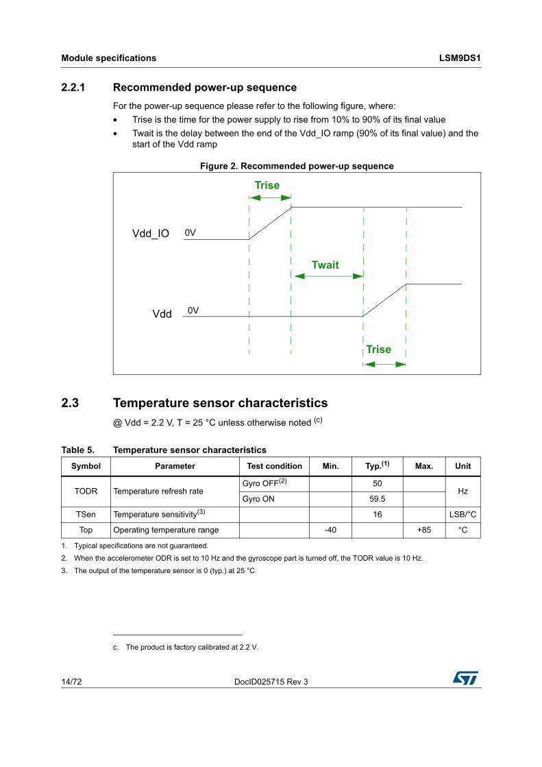
2.2.1 Recommended power-up sequence
For the power-up sequence please refer to the following figure, where:
• Trise is the time for the power supply to rise from 10% to 90% of its final value
• Twait is the delay between the end of the Vdd_IO ramp (90% of its final value) and the start of the Vdd ramp
Figure 2. Recommended power-up sequence
2.3 Temperature sensor characteristics
@ Vdd = 2.2 V, T = 25 °C unless otherwise noted (c)
c. The product is factory calibrated at 2.2 V.
Table 5. Temperature sensor characteristics
Symbol Parameter Test condition Min. Typ.(1) Max. Unit
TODR Temperature refresh rateGyro OFF(2) 50
HzGyro ON 59.5
TSen Temperature sensitivity(3) 16 LSB/°C
Top Operating temperature range -40 +85 °C
1. Typical specifications are not guaranteed.
2. When the accelerometer ODR is set to 10 Hz and the gyroscope part is turned off, the TODR value is 10 Hz.
3. The output of the temperature sensor is 0 (typ.) at 25 °C

DocID025715 Rev 3 15/72
LSM9DS1 Module specifications
72
2.4 Communication interface characteristics
2.4.1 SPI - serial peripheral interface
Subject to general operating conditions for Vdd and Top.
Figure 3. SPI slave timing diagram
Note: Measurement points are done at 0.2·Vdd_IO and 0.8·Vdd_IO, for both input and output ports.
Table 6. SPI slave timing values
Symbol ParameterValue(1)
UnitMin Max
tc(SPC) SPI clock cycle 100 ns
fc(SPC) SPI clock frequency 10 MHz
tsu(CS) CS setup time 5
ns
th(CS) CS hold time 20
tsu(SI) SDI input setup time 5
th(SI) SDI input hold time 15
tv(SO) SDO valid output time 50
th(SO) SDO output hold time 5
tdis(SO) SDO output disable time 50
1. Values are guaranteed at 10 MHz clock frequency for SPI with both 4 and 3 wires, based on characterization results, not tested in production

Module specifications LSM9DS1
16/72 DocID025715 Rev 3
2.4.2 I2C - inter-IC control interface
Subject to general operating conditions for Vdd and Top.
Figure 4. I2C slave timing diagram
Note: Measurement points are done at 0.2·Vdd_IO and 0.8·Vdd_IO, for both ports
Table 7. I2C slave timing values
Symbol ParameterI2C Standard mode(1) I2C Fast mode (1)
UnitMin Max Min Max
f(SCL) SCL clock frequency 0 100 0 400 kHz
tw(SCLL) SCL clock low time 4.7 1.3µs
tw(SCLH) SCL clock high time 4.0 0.6
tsu(SDA) SDA setup time 250 100 ns
th(SDA) SDA data hold time 0 3.45 0 0.9 µs
th(ST) START condition hold time 4 0.6
µs
tsu(SR)Repeated START condition setup time
4.7 0.6
tsu(SP) STOP condition setup time 4 0.6
tw(SP:SR)Bus free time between STOP and START condition
4.7 1.3
1. Data based on standard I2C protocol requirement, not tested in production.
DocID025715 Rev 3 17/72
LSM9DS1 Module specifications
72
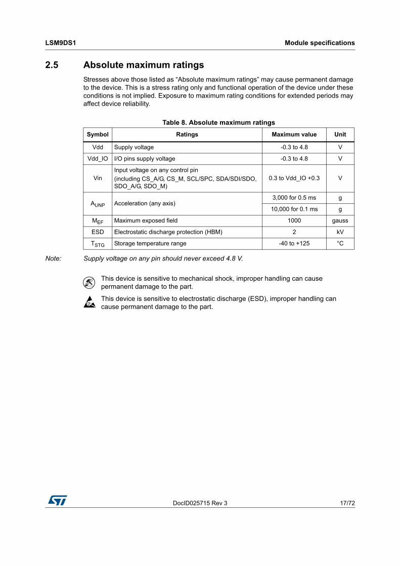
2.5 Absolute maximum ratings
Stresses above those listed as “Absolute maximum ratings” may cause permanent damage to the device. This is a stress rating only and functional operation of the device under these conditions is not implied. Exposure to maximum rating conditions for extended periods may affect device reliability.
Note: Supply voltage on any pin should never exceed 4.8 V.
Table 8. Absolute maximum ratings
Symbol Ratings Maximum value Unit
Vdd Supply voltage -0.3 to 4.8 V
Vdd_IO I/O pins supply voltage -0.3 to 4.8 V
VinInput voltage on any control pin
(including CS_A/G, CS_M, SCL/SPC, SDA/SDI/SDO, SDO_A/G, SDO_M)
0.3 to Vdd_IO +0.3 V
AUNP Acceleration (any axis)3,000 for 0.5 ms g
10,000 for 0.1 ms g
MEF Maximum exposed field 1000 gauss
ESD Electrostatic discharge protection (HBM) 2 kV
TSTG Storage temperature range -40 to +125 °C
This device is sensitive to mechanical shock, improper handling can cause permanent damage to the part.
This device is sensitive to electrostatic discharge (ESD), improper handling can cause permanent damage to the part.

Module specifications LSM9DS1
18/72 DocID025715 Rev 3
2.6 Terminology
2.6.1 Sensitivity
Linear acceleration sensitivity can be determined, for example, by applying 1 g acceleration to the device. Because the sensor can measure DC accelerations, this can be done easily by pointing the selected axis towards the ground, noting the output value, rotating the sensor 180 degrees (pointing towards the sky) and noting the output value again. By doing so, ±1 g acceleration is applied to the sensor. Subtracting the larger output value from the smaller one, and dividing the result by 2, leads to the actual sensitivity of the sensor. This value changes very little over temperature and over time. The sensitivity tolerance describes the range of sensitivities of a large number of sensors.
An angular rate gyroscope is device that produces a positive-going digital output for counterclockwise rotation around the axis considered. Sensitivity describes the gain of the sensor and can be determined by applying a defined angular velocity to it. This value changes very little over temperature and time.
Magnetic sensor sensitivity describes the gain of the sensor and can be determined, for example, by applying a magnetic field of 1 gauss to it.
2.6.2 Zero-g, zero-rate and zero-gauss level
Linear acceleration zero-g level offset (TyOff) describes the deviation of an actual output signal from the ideal output signal if no acceleration is present. A sensor in a steady state on a horizontal surface will measure 0 g on both the X-axis and Y-axis, whereas the Z-axis will measure 1 g. Ideally, the output is in the middle of the dynamic range of the sensor (content of OUT registers 00h, data expressed as two’s complement number). A deviation from the ideal value in this case is called zero-g offset.
Offset is to some extent a result of stress to MEMS sensor and therefore the offset can slightly change after mounting the sensor onto a printed circuit board or exposing it to extensive mechanical stress. Offset changes little over temperature, see “Linear acceleration zero-g level change vs. temperature” in Table 3. The zero-g level tolerance (TyOff) describes the standard deviation of the range of zero-g levels of a group of sensors.
Zero-rate level describes the actual output signal if there is no angular rate present. The zero-rate level of precise MEMS sensors is, to some extent, a result of stress to the sensor and therefore the zero-rate level can slightly change after mounting the sensor onto a printed circuit board or after exposing it to extensive mechanical stress. This value changes very little over temperature and time.
Zero-gauss level offset (M_TyOff) describes the deviation of an actual output signal from the ideal output if no magnetic field is present.

DocID025715 Rev 3 19/72
LSM9DS1 LSM9DS1 functionality
72
3 LSM9DS1 functionality
3.1 Operating modes
In the LSM9DS1 the accelerometer and gyroscope have two operating modes available: only accelerometer active and gyroscope in power down or both accelerometer and gyroscope sensors active at the same ODR. Switching from one mode to the other requires one write operation: writing to CTRL_REG6_XL (20h), the accelerometer operates in normal mode and the gyroscope is powered down, writing to CTRL_REG1_G (10h) both accelerometer and gyroscope are activated at the same ODR.
Figure 5 depicts both modes of operation from power down.
Figure 5. Switching operating modes
The magnetic sensor has three operating modes available: power-down (default), continuous-conversion mode and single-conversion mode. Switching from power-down to the other modes requires one write operation to CTRL_REG3_M (22h), setting values in the MD[1:0] bits. For the output of the magnetic data compensated by temperature, the TEMP_COMP bit in CTRL_REG1_M (20h) must be set to ‘1’.
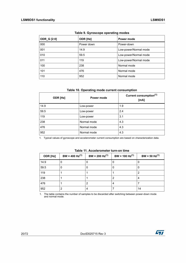
3.2 Gyroscope power modes
In the LSM9DS1, the gyroscope can be configured in three different operating modes: power-down, low-power and normal mode.
Low-power mode is available for lower ODR (14.9, 59.5, 119 Hz) while for greater ODR (238, 476, 952 Hz) the device is automatically in normal mode. Table summarizes the ODR configuration (ODR_G[2:0] bits set in CTRL_REG1_G (10h)) and corresponding power modes.
To enable low-power mode, the LP_mode bit in CTRL_REG3_G (12h) has to be set to ‘1’.
Low-power mode allows reaching low power consumption while maintaining the device always on, refer to Table 10.
LSM9DS1 functionality LSM9DS1
20/72 DocID025715 Rev 3
Table 9. Gyroscope operating modes
ODR_G [2:0] ODR [Hz] Power mode
000 Power down Power-down
001 14.9 Low-power/Normal mode
010 59.5 Low-power/Normal mode
011 119 Low-power/Normal mode
100 238 Normal mode
101 476 Normal mode
110 952 Normal mode
Table 10. Operating mode current consumption
ODR [Hz] Power modeCurrent consumption(1)
[mA]
1. Typical values of gyroscope and accelerometer current consumption are based on characterization data.
14.9 Low-power 1.9
59.5 Low-power 2.4
119 Low-power 3.1
238 Normal mode 4.3
476 Normal mode 4.3
952 Normal mode 4.3
Table 11. Accelerometer turn-on time
ODR [Hz] BW = 400 Hz(1)
1. The table contains the number of samples to be discarded after switching between power-down mode and normal mode.
BW = 200 Hz(1) BW = 100 Hz(1) BW = 50 Hz(1)
14.9 0 0 0 0
59.5 0 0 0 0
119 1 1 1 2
238 1 1 2 4
476 1 2 4 7
952 2 4 7 14

DocID025715 Rev 3 21/72
LSM9DS1 LSM9DS1 functionality
72
3.3 Accelerometer and gyroscope multiple reads (burst)
When only accelerometer is activated and the gyroscope is in power down, starting from OUT_X_XL (28h - 29h) multiple reads can be performed. Once OUT_Z_XL (2Ch - 2Dh) is read, the system automatically restarts from OUT_X_XL (28h - 29h) (see Figure 6).
Figure 6. Multiple reads: accelerometer only
When both accelerometer and gyroscope sensors are activated at the same ODR, starting from OUT_X_G (18h - 19h) multiple reads can be performed. Once OUT_Z_XL (2Ch - 2Dh) is read, the system automatically restarts from OUT_X_G (18h - 19h) (see Figure 7).
Figure 7. Multiple reads: accelerometer and gyroscope
Table 12. Gyroscope turn-on time
ODR [Hz] LPF1 only(1)
1. The table contains the number of samples to be discarded after switching between low-power mode and normal mode.
LPF1 and LPF2(1)
14.9 2 LPF2 not available
59.5 or 119 3 13
238 4 14
476 5 15
952 8 18

LSM9DS1 functionality LSM9DS1
22/72 DocID025715 Rev 3
3.4 Block diagram
Figure 8. Accelerometer and gyroscope digital block diagram
Figure 9. Magnetometer block diagram
DocID025715 Rev 3 23/72
LSM9DS1 LSM9DS1 functionality
72
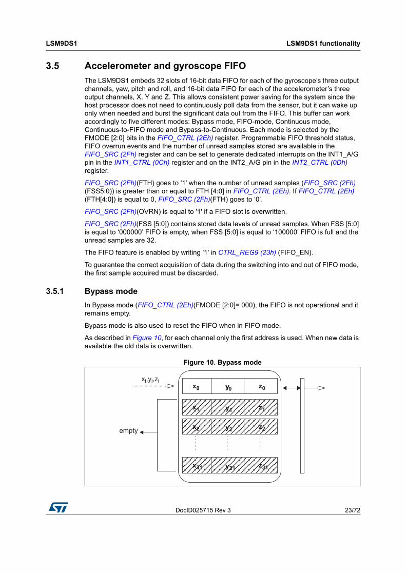
3.5 Accelerometer and gyroscope FIFO
The LSM9DS1 embeds 32 slots of 16-bit data FIFO for each of the gyroscope’s three output channels, yaw, pitch and roll, and 16-bit data FIFO for each of the accelerometer’s three output channels, X, Y and Z. This allows consistent power saving for the system since the host processor does not need to continuously poll data from the sensor, but it can wake up only when needed and burst the significant data out from the FIFO. This buffer can work accordingly to five different modes: Bypass mode, FIFO-mode, Continuous mode, Continuous-to-FIFO mode and Bypass-to-Continuous. Each mode is selected by the FMODE [2:0] bits in the FIFO_CTRL (2Eh) register. Programmable FIFO threshold status, FIFO overrun events and the number of unread samples stored are available in the FIFO_SRC (2Fh) register and can be set to generate dedicated interrupts on the INT1_A/G pin in the INT1_CTRL (0Ch) register and on the INT2_A/G pin in the INT2_CTRL (0Dh) register.
FIFO_SRC (2Fh)(FTH) goes to '1' when the number of unread samples (FIFO_SRC (2Fh) (FSS5:0)) is greater than or equal to FTH [4:0] in FIFO_CTRL (2Eh). If FIFO_CTRL (2Eh) (FTH[4:0]) is equal to 0, FIFO_SRC (2Fh)(FTH) goes to ‘0’.
FIFO_SRC (2Fh)(OVRN) is equal to '1' if a FIFO slot is overwritten.
FIFO_SRC (2Fh)(FSS [5:0]) contains stored data levels of unread samples. When FSS [5:0] is equal to ‘000000’ FIFO is empty, when FSS [5:0] is equal to ‘100000’ FIFO is full and the unread samples are 32.
The FIFO feature is enabled by writing '1' in CTRL_REG9 (23h) (FIFO_EN).
To guarantee the correct acquisition of data during the switching into and out of FIFO mode, the first sample acquired must be discarded.
3.5.1 Bypass mode
In Bypass mode (FIFO_CTRL (2Eh)(FMODE [2:0]= 000), the FIFO is not operational and it remains empty.
Bypass mode is also used to reset the FIFO when in FIFO mode.
As described in Figure 10, for each channel only the first address is used. When new data is available the old data is overwritten.
Figure 10. Bypass mode
x0 y z0y0
x1 y1 z1
x2 y2 z2
x31 y31 z31
xi,yi,zi
empty

LSM9DS1 functionality LSM9DS1
24/72 DocID025715 Rev 3
3.5.2 FIFO mode
In FIFO mode (FIFO_CTRL (2Eh) (FMODE [2:0] = 001) data from the output channels are stored in the FIFO until it is overwritten.
To reset FIFO content, Bypass mode should be selected by writing FIFO_CTRL (2Eh) (FMODE [2:0]) to '000'. After this reset command, it is possible to restart FIFO mode by writing FIFO_CTRL (2Eh) (FMODE [2:0]) to '001'.
The FIFO buffer memorizes 32 levels of data but the depth of the FIFO can be resized by setting the STOP_ON_FTH bit in CTRL_REG9 (23h). If the STOP_ON_FTH bit is set to '1', FIFO depth is limited to FIFO_CTRL (2Eh)(FTH [4:0]) + 1 data.
A FIFO threshold interrupt can be enabled (INT_OVR bit in INT1_CTRL (0Ch) ) in order to be raised when the FIFO is filled to the level specified by the FTH[4:0] bits of FIFO_CTRL (2Eh). When a FIFO threshold interrupt occurs, the first data has been overwritten and the FIFO stops collecting data from the input channels.
Figure 11. FIFO mode
3.5.3 Continuous mode
Continuous mode (FIFO_CTRL (2Eh)(FMODE[2:0] = 110) provides continuous FIFO update: as new data arrives the older is discarded.
A FIFO threshold flag FIFO_SRC (2Fh)(FTH) is asserted when the number of unread samples in FIFO is greater than or equal to FIFO_CTRL (2Eh)(FTH4:0).
It is possible to route FIFO_SRC (2Fh)(FTH) to the INT1_A/G pin by writing in register INT1_CTRL (0Ch) (INT1_FTH) = '1', or to the INT2_A/G pin by writing in register INT2_CTRL (0Dh) (INT2_FTH) = '1'.
A full-flag interrupt can be enabled, (INT1_CTRL (0Ch) (INT_ FSS5)= '1’) when the FIFO becomes saturated and in order to read the contents all at once.
If an overrun occurs, the oldest sample in FIFO is overwritten and the OVRN flag in FIFO_SRC (2Fh) is asserted.
In order to empty the FIFO before it is full it is also possible to pull from FIFO the number of unread samples available in FIFO_SRC (2Fh) (FSS[5:0]).

DocID025715 Rev 3 25/72
LSM9DS1 LSM9DS1 functionality
72
Figure 12. Continuous mode
3.5.4 Continuous-to-FIFO mode
In Continuous-to-FIFO mode (FIFO_CTRL (2Eh)(FMODE [2:0] = 011), FIFO behavior changes according to the INT_GEN_SRC_XL (26h)(IA_XL) bit. When the INT_GEN_SRC_XL (26h)(IA_XL) bit is equal to '1', FIFO operates in FIFO-mode, when the INT_GEN_SRC_XL (26h)(IA_XL) bit is equal to '0', FIFO operates in Continuous mode.
The interrupt generator should be set to the desired configuration by means of INT_GEN_CFG_XL (06h), INT_GEN_THS_X_XL (07h), INT_GEN_THS_Y_XL (08h) and INT_GEN_THS_Z_XL (09h).
The CTRL_REG4 (1Eh)(LIR_XL) bit should be set to '1' in order to have latched interrupt.
Figure 13. Continuous-to-FIFO mode
x0 y0 z0
x1 y1 z1
x2 y2 z2
x31 y31 z31
xi,yi,zi
x30 y30 z30
x0 y z0y0
x1 y1 z1
x2 y2 z2
x31 y31 z31
xi,yi,zi
Continuous Mode FIFO Mode
Trigger event
x0 y0 z0
x1 y1 z1
x2 y2 z2
x31 y31 z31
xi,yi,zi
x30 y30 z30

LSM9DS1 functionality LSM9DS1
26/72 DocID025715 Rev 3
3.5.5 Bypass-to-Continuous mode
In Bypass-to-Continuous mode (FIFO_CTRL (2Eh)(FMODE[2:0] = '100'), data measurement storage inside FIFO operates in Continuous mode when INT_GEN_SRC_XL (26h)(IA_XL) is equal to '1', otherwise FIFO content is reset (Bypass mode).
The interrupt generator should be set to the desired configuration by means of INT_GEN_CFG_XL (06h), INT_GEN_THS_X_XL (07h), INT_GEN_THS_Y_XL (08h) and INT_GEN_THS_Z_XL (09h).
The CTRL_REG4 (1Eh)(LIR_XL) bit should be set to '1' in order to have latched interrupt.
Figure 14. Bypass-to-Continuous mode
x0 yi z0y0
x1 y1 z1
x2 y2 z2
x31 y31 z31
xi,yi,zi
empty
Bypass Mode Continuous Mode
Trigger event
x0 y0 z0
x1 y1 z1
x2 y2 z2
x31 y31 z31
xi,yi,zi
x30 y30 z30

DocID025715 Rev 3 27/72
LSM9DS1 Application hints
72
4 Application hints
Figure 15. LSM9DS1 electrical connections
4.1 External capacitors
The device core is supplied through the Vdd line. Power supply decoupling capacitors (C2, C3 = 100 nF ceramic, C4 = 10 µF Al) should be placed as near as possible to the supply pin of the device (common design practice). Capacitor C1 (100 nF) should be a capacitor with low ESR value and should be placed as near as possible to the C1 pin.
All voltage and ground supplies must be present at the same time to achieve proper behavior of the IC (refer to Figure 15).

Digital interfaces LSM9DS1
28/72 DocID025715 Rev 3
5 Digital interfaces
The registers embedded inside the LSM9DS1 may be accessed through both the I2C and SPI serial interfaces. The latter may be SW configured to operate either in 3-wire or 4-wire interface mode.
The serial interfaces are mapped onto the same pins. To select/exploit the I2C interface, the CS line must be tied high (i.e connected to Vdd_IO).
5.1 I2C serial interface
The LSM9DS1 I2C is a bus slave. The I2C is employed to write the data to the registers, whose content can also be read back.
The relevant I2C terminology is provided in the table below.
There are two signals associated with the I2C bus: the serial clock line (SCL) and the Serial DAta line (SDA). The latter is a bidirectional line used for sending and receiving the data to/from the interface. Both the lines must be connected to Vdd_IO through an external pull-up resistor. When the bus is free, both the lines are high.
The I2C interface is implemented with fast mode (400 kHz) I2C standards as well as with the standard mode.
In order to disable the I2C block for accelerometer and gyroscope the I2C_DISABLE bit must be written to ‘1’ in CTRL_REG9 (23h), while for magnetometer the I2C_DISABLE bit must be written to ‘1’ in CTRL_REG3_M (22h).
Table 13. Serial interface pin description
Pin name Pin description
CS_A/G, CS_MSPI enable
I2C/SPI mode selection (1: SPI idle mode / I2C communication enabled; 0: SPI communication mode / I2C disabled)
SCL/SPCI2C Serial Clock (SCL)
SPI Serial Port Clock (SPC)
SDA/SDI/SDO
I2C Serial Data (SDA)
SPI Serial Data Input (SDI)
3-wire Interface Serial Data Output (SDO)
SDO_A/G, SDO_MSPI Serial Data Output (SDO)
I2C less significant bit of the device address
Table 14. I2C terminology
Term Description
Transmitter The device which sends data to the bus
Receiver The device which receives data from the bus
MasterThe device which initiates a transfer, generates clock signals and terminates a transfer
Slave The device addressed by the master

DocID025715 Rev 3 29/72
LSM9DS1 Digital interfaces
72
5.1.1 I2C operation
The transaction on the bus is started through a START (ST) signal. A START condition is defined as a high-to-low transition on the data line while the SCL line is held high. After this has been transmitted by the master, the bus is considered busy. The next byte of data transmitted after the start condition contains the address of the slave in the first 7 bits and the eighth bit tells whether the master is receiving data from the slave or transmitting data to the slave. When an address is sent, each device in the system compares the first seven bits after a start condition with its address. If they match, the device considers itself addressed by the master.
Data transfer with acknowledge is mandatory. The transmitter must release the SDA line during the acknowledge pulse. The receiver must then pull the data line low so that it remains stable low during the high period of the acknowledge clock pulse. A receiver which has been addressed is obliged to generate an acknowledge after each byte of data received.
The I2C embedded inside the LSM9DS1 behaves like a slave device and the following protocol must be adhered to. In the I2C of the accelerometer and gyroscope sensor, after the start condition (ST) a slave address is sent, once a slave acknowledge (SAK) has been returned, an 8-bit sub-address (SUB) is transmitted. The 7 LSb represent the actual register address while the CTRL_REG8 (22h) (IF_ADD_INC) bit defines the address increment. In the I2C of the magnetometer sensor, after the START condition (ST) a slave address is sent, once a slave acknowledge (SAK) has been returned, an 8-bit sub-address (SUB) is transmitted. The 7 LSb represent the actual register address while the MSB enables the address auto increment. The SUB (register address) is automatically increased to allow multiple data read/write.
Data are transmitted in byte format (DATA). Each data transfer contains 8 bits. The number of bytes transferred per transfer is unlimited. Data is transferred with the Most Significant bit (MSb) first. If a receiver can’t receive another complete byte of data until it has performed
Table 15. Transfer when master is writing one byte to slave
Master ST SAD + W SUB DATA SP
Slave SAK SAK SAK
Table 16. Transfer when master is writing multiple bytes to slave
Master ST SAD + W SUB DATA DATA SP
Slave SAK SAK SAK SAK
Table 17. Transfer when master is receiving (reading) one byte of data from slave
Master ST SAD + W SUB SR SAD + R NMAK SP
Slave SAK SAK SAK DATA
Table 18. Transfer when master is receiving (reading) multiple bytes of data from slave
Master ST SAD+W SUB SR SAD+R MAK MAK NMAK SP
Slave SAK SAK SAK DATA DATA DATA

Digital interfaces LSM9DS1
30/72 DocID025715 Rev 3
some other function, it can hold the clock line, SCL low to force the transmitter into a wait state. Data transfer only continues when the receiver is ready for another byte and releases the data line. If a slave receiver doesn’t acknowledge the slave address (i.e. it is not able to receive because it is performing some real-time function) the data line must be left high by the slave. The master can then abort the transfer. A low-to-high transition on the SDA line while the SCL line is high is defined as a STOP condition. Each data transfer must be terminated by the generation of a STOP (SP) condition.
In the presented communication format MAK is Master acknowledge and NMAK is No Master Acknowledge.
Default address:
The slave address is completed with a Read/Write bit. If the bit was ‘1’ (Read), a repeated START (SR) condition must be issued after the two sub-address bytes. If the bit is ‘0’ (Write) the master will transmit to the slave with direction unchanged. Table 19 and Table 20 explain how the SAD+Read/Write bit pattern is composed, listing all the possible configurations.
Table 19. Accelerometer and gyroscope SAD+Read/Write patterns
Table 20. Magnetic sensor SAD+Read/Write patterns
Command SAD[6:1] SAD[0] = SA0 R/W SAD+R/W
Read 110101 0 1 11010101 (D5h)
Write 110101 0 0 11010100 (D4h)
Read 110101 1 1 11010111 (D7h)
Write 110101 1 0 11010110 (D6h)
Command SAD[6:2] SAD[1] = SDO/SA1 SAD[0] R/W SAD+R/W
Read 00111 0 0 1 00111001 (39h)
Write 00111 0 0 0 00111000 (38h)
Read 00111 1 0 1 00111101 (3Dh)
Write 00111 1 0 0 00111100 (3Ch)

DocID025715 Rev 3 31/72
LSM9DS1 Digital interfaces
72
5.2 Accelerometer and gyroscope SPI bus interface
The LSM9DS1 accelerometer and gyroscope SPI is a bus slave. The SPI allows to write and read the registers of the device.
The Serial Interface connects to applications using 4 wires: CS_A/G, SPC, SDI and SDO_A/G.
Figure 16. Accelerometer and gyroscope read and write protocol
CS_A/G is the serial port enable and it is controlled by the SPI master. It goes low at the start of the transmission and goes back high at the end. SPC is the serial port clock and it is controlled by the SPI master. It is stopped high when CS_A/G is high (no transmission). SDI and SDO_A/G are respectively the serial port data input and output. Those lines are driven at the falling edge of SPC and should be captured at the rising edge of SPC.
Both the read register and write register commands are completed in 16 clock pulses or in multiples of 8 in case of multiple read/write bytes. Bit duration is the time between two falling edges of SPC. The first bit (bit 0) starts at the first falling edge of SPC after the falling edge of CS_A/G while the last bit (bit 15, bit 23, ...) starts at the last falling edge of SPC just before the rising edge of CS_A/G.
bit 0: RW bit. When 0, the data DI(7:0) is written into the device. When 1, the data DO(7:0) from the device is read. In latter case, the chip will drive SDO_A/G at the start of bit 8.
bit 1-7: address AD(6:0). This is the address field of the indexed register.
bit 8-15: data DI(7:0) (write mode). This is the data that is written into the device (MSb first).
bit 8-15: data DO(7:0) (read mode). This is the data that is read from the device (MSb first).
In multiple read/write commands further blocks of 8 clock periods will be added. When the CTRL_REG8 (22h) (IF_ADD_INC) bit is ‘0’ the address used to read/write data remains the same for every block. When the CTRL_REG8 (22h)(IF_ADD_INC) bit is ‘1’, the address used to read/write data is increased at every block.
The function and the behavior of SDI and SDO_A/G remain unchanged.

Digital interfaces LSM9DS1
32/72 DocID025715 Rev 3
5.2.1 SPI read
Figure 17. Accelerometer and gyroscope SPI read protocol
The SPI read command is performed with 16 clock pulses. A multiple byte read command is performed by adding blocks of 8 clock pulses to the previous one.
bit 0: READ bit. The value is 1.
bit 1-7: address AD(6:0). This is the address field of the indexed register.
bit 8-15: data DO(7:0) (read mode). This is the data that will be read from the device (MSb first).
bit 16-... : data DO(...-8). Further data in multiple byte reads.
Figure 18. Multiple byte SPI read protocol (2-byte example)

DocID025715 Rev 3 33/72
LSM9DS1 Digital interfaces
72
5.2.2 SPI write
Figure 19. Accelerometer and gyroscope SPI write protocol
The SPI write command is performed with 16 clock pulses. A multiple byte write command is performed by adding blocks of 8 clock pulses to the previous one.
bit 0: WRITE bit. The value is 0.
bit 1 -7: address AD(6:0). This is the address field of the indexed register.
bit 8-15: data DI(7:0) (write mode). This is the data that is written inside the device (MSb first).
bit 16-... : data DI(...-8). Further data in multiple byte writes.
Figure 20. Multiple byte SPI write protocol (2-byte example)
5.2.3 SPI read in 3-wire mode
3-wire mode is entered by setting the CTRL_REG8 (22h)(SIM) bit equal to ‘1’ (SPI serial interface mode selection).
Figure 21. Accelerometer and gyroscope SPI read protocol in 3-wire mode
The SPI read command is performed with 16 clock pulses:
bit 0: READ bit. The value is 1.
bit 1-7: address AD(6:0). This is the address field of the indexed register.
bit 8-15: data DO(7:0) (read mode). This is the data that is read from the device (MSb first).
A multiple read command is also available in 3-wire mode.

Digital interfaces LSM9DS1
34/72 DocID025715 Rev 3
5.3 Magnetic sensor SPI bus interface
The LSM9DS1 magnetic sensor SPI is a bus slave. The SPI allows writing and reading the registers of the device.
The serial interface connects to applications using 4 wires: CS_M, SPC, SDI and SDO_M.
Figure 22. Magnetic sensor read and write protocol
CS_M is the serial port enable and it is controlled by the SPI master. It goes low at the start of the transmission and goes back high at the end. SPC is the serial port clock and it is controlled by the SPI master. It is stopped high when CS_M is high (no transmission). SDI and SDO_M are respectively the serial port data input and output. Those lines are driven at the falling edge of SPC and should be captured at the rising edge of SPC.
Both the read register and write register commands are completed in 16 clock pulses or in multiples of 8 in case of multiple read/write bytes. Bit duration is the time between two falling edges of SPC. The first bit (bit 0) starts at the first falling edge of SPC after the falling edge of CS_M while the last bit (bit 15, bit 23, ...) starts at the last falling edge of SPC just before the rising edge of CS_M.
bit 0: RW bit. When 0, the data DI(7:0) is written into the device. When 1, the data DO(7:0) from the device is read. In latter case, the chip will drive SDO_M at the start of bit 8.
bit 1: MS bit. When 0, the address will remain unchanged in multiple read/write commands. When 1, the address is auto-incremented in multiple read/write commands.
bit 2-7: address AD(5:0). This is the address field of the indexed register.
bit 8-15: data DI(7:0) (write mode). This is the data that is written into the device (MSb first).
bit 8-15: data DO(7:0) (read mode). This is the data that is read from the device (MSb first).
In multiple read/write commands further blocks of 8 clock periods will be added. When the MS bit is ‘0’, the address used to read/write data remains the same for every block. When the MS bit is ‘1’, the address used to read/write data is increased at every block.
The function and the behavior of SDI and SDO_M remain unchanged.

DocID025715 Rev 3 35/72
LSM9DS1 Digital interfaces
72
5.3.1 SPI read
Figure 23. Magnetic sensor SPI read protocol
The SPI read command is performed with 16 clock pulses. A multiple byte read command is performed by adding blocks of 8 clock pulses to the previous one.
bit 0: READ bit. The value is 1.
bit 1: MS bit. When 0, does not increment the address; when 1, increments the address in multiple reads.
bit 2-7: address AD(5:0). This is the address field of the indexed register.
bit 8-15: data DO(7:0) (read mode). This is the data that will be read from the device (MSb first).
bit 16-... : data DO(...-8). Further data in multiple byte reads.
Figure 24. Multiple byte SPI read protocol (2-byte example)
C S
SPC
SDI
SD O
RW
DO 7 DO 6 DO 5 DO 4 DO 3 DO 2 DO 1 DO 0
A D5 A D4 AD 3 A D2 A D1 A D0
DO 15 DO 14 DO 13 DO 12 DO 11 DO 10 D O9 D O8
M S
CS_M
SDO_M

Digital interfaces LSM9DS1
36/72 DocID025715 Rev 3
5.3.2 SPI write
Figure 25. Magnetic sensor SPI write protocol
The SPI write command is performed with 16 clock pulses. A multiple byte write command is performed by adding blocks of 8 clock pulses to the previous one.
bit 0: WRITE bit. The value is 0.
bit 1: MS bit. When 0, does not increment the address; when 1, increments the address in multiple writes.
bit 2 -7: address AD(5:0). This is the address field of the indexed register.
bit 8-15: data DI(7:0) (write mode). This is the data that is written inside the device (MSb first).
bit 16-... : data DI(...-8). Further data in multiple byte writes.
Figure 26. Multiple byte SPI write protocol (2-byte example)
CS
SPC
SDIRW D I7 D I6 D I5 D I4 DI3 DI2 DI1 DI0
AD5 AD 4 AD 3 AD2 AD 1 AD0MS
CS_M
CS
SPC
SDI
RW
AD5 AD4 AD3 AD2 AD1 AD 0
DI7 D I6 DI5 D I4 DI3 DI2 DI1 DI0 DI15 D I1 4 DI13 D I1 2 DI11 DI10 DI9 DI8
MS
CS_M
SPC
SDI

DocID025715 Rev 3 37/72
LSM9DS1 Digital interfaces
72
5.3.3 SPI read in 3-wire mode
3-wire mode is entered by setting the SIM bit to ‘1’ (SPI serial interface mode selection) in CTRL_REG3_M (22h).
When 3-wire mode is used, the SDO_M pin has to be connected to GND or Vdd_IO.
Figure 27. SPI read protocol in 3-wire mode
The SPI read command is performed with 16 clock pulses:
bit 0: READ bit. The value is 1.
bit 1: MS bit. When 0, does not increment the address; when 1, increments the address in multiple reads.
bit 2-7: address AD(5:0). This is the address field of the indexed register.
bit 8-15: data DO(7:0) (read mode). This is the data that is read from the device (MSb first).
A multiple read command is also available in 3-wire mode.
CS
SPC
SDI/ORW D O7 D O6 D O5 DO4 DO3 DO2 DO1 DO0
AD5 AD 4 AD 3 AD2 AD1 AD 0MS
CS_M

Register mapping LSM9DS1
38/72 DocID025715 Rev 3
6 Register mapping
The table given below provides a list of the 8/16-bit registers embedded in the device and the corresponding addresses.
Table 21. Accelerometer and gyroscope register address map
Name TypeRegister address
Default NoteHex Binary
Reserved -- 00-03 -- -- Reserved
ACT_THS r/w 04 00000100 00000000
ACT_DUR r/w 05 00000101 00000000
INT_GEN_CFG_XL r/w 06 00000110 00000000
INT_GEN_THS_X_XL r/w 07 00000111 00000000
INT_GEN_THS_Y_XL r/w 08 00001000 00000000
INT_GEN_THS_Z_XL r/w 09 00001001 00000000
INT_GEN_DUR_XL r/w 0A 00001010 00000000
REFERENCE_G r/w 0B 00001011 00000000
INT1_CTRL r/w 0C 00001100 00000000
INT2_CTRL r/w 0D 00001101 00000000
Reserved -- 0E -- -- Reserved
WHO_AM_I r 0F 00001111 01101000
CTRL_REG1_G r/w 10 00010000 00000000
CTRL_REG2_G r/w 11 00010001 00000000
CTRL_REG3_G r/w 12 00010010 00000000
ORIENT_CFG_G r/w 13 00010011 00000000
INT_GEN_SRC_G r 14 00010100 output
OUT_TEMP_L r 15 00010101 output
OUT_TEMP_H r 16 00010110 output
STATUS_REG r 17 00010111 output
OUT_X_L_G r 18 00011000 output
OUT_X_H_G r 19 00011001 output
OUT_Y_L_G r 1A 00011010 output
OUT_Y_H_G r 1B 00011011 output
OUT_Z_L_G r 1C 00011100 output
OUT_Z_H_G r 1D 00011101 output
CTRL_REG4 r/w 1E 00011110 00111000
CTRL_REG5_XL r/w 1F 00011111 00111000
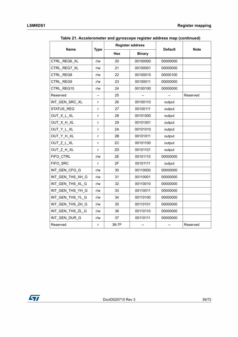
DocID025715 Rev 3 39/72
LSM9DS1 Register mapping
72
CTRL_REG6_XL r/w 20 00100000 00000000
CTRL_REG7_XL r/w 21 00100001 00000000
CTRL_REG8 r/w 22 00100010 00000100
CTRL_REG9 r/w 23 00100011 00000000
CTRL_REG10 r/w 24 00100100 00000000
Reserved -- 25 -- -- Reserved
INT_GEN_SRC_XL r 26 00100110 output
STATUS_REG r 27 00100111 output
OUT_X_L_XL r 28 00101000 output
OUT_X_H_XL r 29 00101001 output
OUT_Y_L_XL r 2A 00101010 output
OUT_Y_H_XL r 2B 00101011 output
OUT_Z_L_XL r 2C 00101100 output
OUT_Z_H_XL r 2D 00101101 output
FIFO_CTRL r/w 2E 00101110 00000000
FIFO_SRC r 2F 00101111 output
INT_GEN_CFG_G r/w 30 00110000 00000000
INT_GEN_THS_XH_G r/w 31 00110001 00000000
INT_GEN_THS_XL_G r/w 32 00110010 00000000
INT_GEN_THS_YH_G r/w 33 00110011 00000000
INT_GEN_THS_YL_G r/w 34 00110100 00000000
INT_GEN_THS_ZH_G r/w 35 00110101 00000000
INT_GEN_THS_ZL_G r/w 36 00110110 00000000
INT_GEN_DUR_G r/w 37 00110111 00000000
Reserved r 38-7F -- -- Reserved
Table 21. Accelerometer and gyroscope register address map (continued)
Name TypeRegister address
Default NoteHex Binary
Register mapping LSM9DS1
40/72 DocID025715 Rev 3
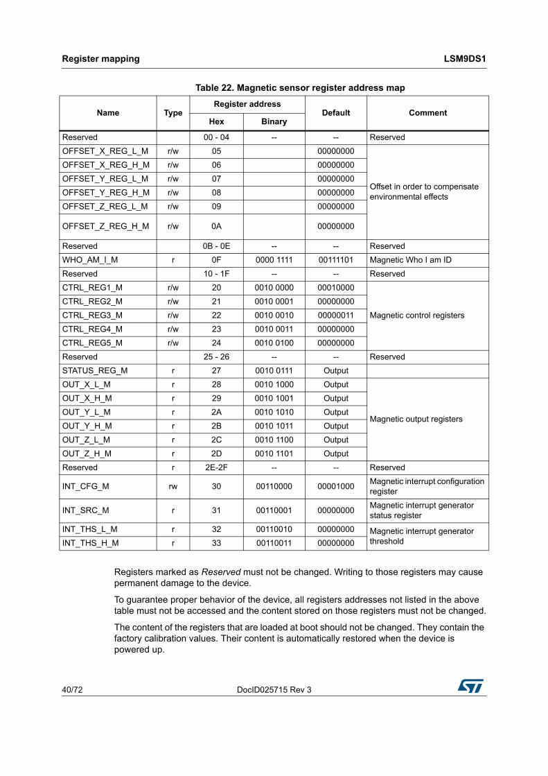
Table 22. Magnetic sensor register address map
Registers marked as Reserved must not be changed. Writing to those registers may cause permanent damage to the device.
To guarantee proper behavior of the device, all registers addresses not listed in the above table must not be accessed and the content stored on those registers must not be changed.
The content of the registers that are loaded at boot should not be changed. They contain the factory calibration values. Their content is automatically restored when the device is powered up.
Name TypeRegister address
Default CommentHex Binary
Reserved 00 - 04 -- -- Reserved
OFFSET_X_REG_L_M r/w 05 00000000
Offset in order to compensate environmental effects
OFFSET_X_REG_H_M r/w 06 00000000
OFFSET_Y_REG_L_M r/w 07 00000000
OFFSET_Y_REG_H_M r/w 08 00000000
OFFSET_Z_REG_L_M r/w 09 00000000
OFFSET_Z_REG_H_M r/w 0A 00000000
Reserved 0B - 0E -- -- Reserved
WHO_AM_I_M r 0F 0000 1111 00111101 Magnetic Who I am ID
Reserved 10 - 1F -- -- Reserved
CTRL_REG1_M r/w 20 0010 0000 00010000
Magnetic control registers
CTRL_REG2_M r/w 21 0010 0001 00000000
CTRL_REG3_M r/w 22 0010 0010 00000011
CTRL_REG4_M r/w 23 0010 0011 00000000
CTRL_REG5_M r/w 24 0010 0100 00000000
Reserved 25 - 26 -- -- Reserved
STATUS_REG_M r 27 0010 0111 Output
OUT_X_L_M r 28 0010 1000 Output
Magnetic output registers
OUT_X_H_M r 29 0010 1001 Output
OUT_Y_L_M r 2A 0010 1010 Output
OUT_Y_H_M r 2B 0010 1011 Output
OUT_Z_L_M r 2C 0010 1100 Output
OUT_Z_H_M r 2D 0010 1101 Output
Reserved r 2E-2F -- -- Reserved
INT_CFG_M rw 30 00110000 00001000Magnetic interrupt configuration register
INT_SRC_M r 31 00110001 00000000Magnetic interrupt generator status register
INT_THS_L_M r 32 00110010 00000000 Magnetic interrupt generator thresholdINT_THS_H_M r 33 00110011 00000000

DocID025715 Rev 3 41/72
LSM9DS1 Accelerometer and gyroscope register description
72
7 Accelerometer and gyroscope register description
The device contains a set of registers which are used to control its behavior and to retrieve linear acceleration, angular rate and temperature data. The register addresses, made up of 7 bits, are used to identify them and to write the data through the serial interface.
7.1 ACT_THS (04h)
Activity threshold register.
Table 24. ACT_THS register description
7.2 ACT_DUR (05h)
Inactivity duration register.
Table 26. ACT_DUR register description
7.3 INT_GEN_CFG_XL (06h)
Linear acceleration sensor interrupt generator configuration register.
Table 23. ACT_THS register
SLEEP_ON_INACT_EN
ACT_THS6
ACT_THS5
ACT_THS4
ACT_THS3
ACT_THS2
ACT_THS1
ACT_THS0
SLEEP_ON_INACT_EN
Gyroscope operating mode during inactivity. Default value: 0
(0: gyroscope in power-down; 1: gyroscope in sleep mode)
ACT_THS [6:0] Inactivity threshold. Default value: 000 0000
Table 25. ACT_DUR register
ACT_DUR7
ACT_DUR6
ACT_DUR5
ACT_DUR4
ACT_DUR3
ACT_DUR2
ACT_DUR1
ACT_DUR0
ACT_DUR [7:0] Inactivity duration. Default value: 0000 0000
Table 27. INT_GEN_CFG_XL register
AOI_XL 6D ZHIE_XL ZLIE_XL YHIE_XL YLIE_XL XHIE_XL XLIE_XL

Accelerometer and gyroscope register description LSM9DS1
42/72 DocID025715 Rev 3
Table 28. INT_GEN_CFG_XL register description
7.4 INT_GEN_THS_X_XL (07h)
Linear acceleration sensor interrupt threshold register.
Table 30. INT_GEN_THS_X_XL register description
7.5 INT_GEN_THS_Y_XL (08h)
Linear acceleration sensor interrupt threshold register.
Table 32. INT_GEN_THS_Y_XL register description
AOI_XL AND/OR combination of accelerometer’s interrupt events. Default value: 0(0: OR combination; 1: AND combination)
6D 6-direction detection function for interrupt. Default value: 0
(0: disabled; 1: enabled)
ZHIE_XL Enable interrupt generation on accelerometer’s Z-axis high event. Default value: 0
(0: disable interrupt request; 1: interrupt request on measured acceleration value
higher than preset threshold)
ZLIE_XL Enable interrupt generation on accelerometer’s Z-axis low event. Default value: 0
(0: disable interrupt request; 1: interrupt request on measured acceleration value
lower than preset threshold)
YHIE_XL Enable interrupt generation on accelerometer’s Y-axis high event. Default value: 0
(0: disable interrupt request; 1: interrupt request on measured acceleration value
higher than preset threshold)
YLIE_XL Enable interrupt generation on accelerometer’s Y-axis low event. Default value: 0
(0: disable interrupt request; 1: interrupt request on measured acceleration value
lower than preset threshold)
XHIE_XL Enable interrupt generation on accelerometer’s X-axis high event. Default value: 0
(0: disable interrupt request; 1: interrupt request on measured acceleration value
higher than preset threshold)
XLIE_XL Enable interrupt generation on accelerometer’s X-axis low event. Default value: 0
(0: disable interrupt request; 1: interrupt request on measured acceleration value
lower than preset threshold)
Table 29. INT_GEN_THS_X_XL register
THS_XL_X7
THS_XL_X6
THS_XL_X5
THS_XL_X4
THS_XL_X3
THS_XL_X2
THS_XL_X1
THS_XL_X0
THS_XL_X [7:0] X-axis interrupt threshold. Default value: 0000 0000
Table 31. INT_GEN_THS_Y_XL register
THS_XL_Y7
THS_XL_Y6
THS_XL_Y5
THS_XL_Y4
THS_XL_Y3
THS_XL_Y2
THS_XL_Y1
THS_XL_Y0
THS_XL_Y [7:0] Y-axis interrupt threshold. Default value: 0000 0000

DocID025715 Rev 3 43/72
LSM9DS1 Accelerometer and gyroscope register description
72
7.6 INT_GEN_THS_Z_XL (09h)
Linear acceleration sensor interrupt threshold register.
Table 34. INT_GEN_THS_Z_XL register description
7.7 INT_GEN_DUR_XL (0Ah)
Linear acceleration sensor interrupt duration register.
Table 35. INT_GEN_DUR_XL register
Table 36. INT_GEN_DUR_XL register description
7.8 REFERENCE_G (0Bh)
Angular rate sensor reference value register for digital high-pass filter (r/w).
Table 37. REFERENCE_G register
Table 38. REFERENCE_G register description
7.9 INT1_CTRL (0Ch)
INT1_A/G pin control register.
Table 39. INT1_CTRL register
Table 33. INT_GEN_THS_Z_XL register
THS_XL_Z7
THS_XL_Z6
THS_XL_Z5
THS_XL_Z4
THS_XL_Z3
THS_XL_Z2
THS_XL_Z1
THS_XL_Z0
THS_XL_Z [7:0] Z-axis interrupt threshold. Default value: 0000 0000
WAIT_XL DUR_XL6 DUR_XL5 DUR_XL4 DUR_XL3 DUR_XL2 DUR_XL1 DUR_XL0
WAIT_XL Wait function enabled on duration counter. Default value: 0
(0: wait function off; 1: wait for DUR_XL [6:0] samples before exiting interrupt)
DUR_XL [6:0] Enter/exit interrupt duration value. Default value: 000 0000
REF7_G REF6_G REF5_G REF4_G REF3_G REF2_G REF1_G REF0_G
REF_G [7:0] Reference value for gyroscope’s digital high-pass filter (r/w).
Default value: 0000 0000
INT1_IG _G
INT1_IG_XL
INT1_ FSS5
INT1_OVR INT1_FTH INT1_ BootINT1_
DRDY_GINT1_
DRDY_XL

Accelerometer and gyroscope register description LSM9DS1
44/72 DocID025715 Rev 3
Table 40. INT1_CTRL register description
7.10 INT2_CTRL (0Dh)
INT2_A/G pin control register.
Table 41. INT2_CTRL register
Table 42. INT2_CTRL register description
INT1_IG_GGyroscope interrupt enable on INT 1_A/G pin. Default value: 0
(0: disabled; 1: enabled)
INT_ IG_XLAccelerometer interrupt generator on INT 1_A/G pin. Default value: 0
(0: disabled; 1: enabled)
INT_ FSS5FSS5 interrupt enable on INT 1_A/G pin. Default value: 0
(0: disabled; 1: enabled)
INT_OVR Overrun interrupt on INT 1_A/G pin. Default value: 0(0: disabled; 1: enabled)
INT_FTHFIFO threshold interrupt on INT 1_A/G pin. Default value: 0
(0: disabled; 1: enabled)
INT_ BootBoot status available on INT 1_A/G pin. Default value: 0
(0: disabled; 1: enabled)
INT_DRDY_GGyroscope data ready on INT 1_A/G pin. Default value: 0
(0: disabled; 1: enabled)
INT_DRDY_XLAccelerometer data ready on INT 1_A/G pin. Default value: 0
(0: disabled; 1: enabled)
INT2_INACT
0INT2_ FSS5
INT2_OVR INT2_FTHINT2_
DRDY_TEMP
INT2_ DRDY_G
INT2_
DRDY_XL
INT2_INACTInactivity interrupt output signal. Default value: 0(0: no interrupt has been generated; 1: one or more interrupt events have been generated)
INT2_ FSS5FSS5 interrupt enable on INT2_A/G pin. Default value: 0
(0: disabled; 1: enabled)
INT2_OVR Overrun interrupt on INT2_A/G pin. Default value: 0(0: disabled; 1: enabled)
INT2_FTHFIFO threshold interrupt on INT2_A/G pin. Default value: 0
(0: disabled; 1: enabled)
INT2_ DRDY_TEMP
Temperature data ready on INT2_A/G pin. Default value: 0
(0: disabled; 1: enabled)
INT2_DRDY_GGyroscope data ready on INT2_A/G pin. Default value: 0
(0: disabled; 1: enabled)
INT2_DRDY_XLAccelerometer data ready on INT2_A/G pin. Default value: 0
(0: disabled; 1: enabled)

DocID025715 Rev 3 45/72
LSM9DS1 Accelerometer and gyroscope register description
72
7.11 WHO_AM_I (0Fh)
Who_AM_I register.
7.12 CTRL_REG1_G (10h)
Angular rate sensor Control Register 1.
Table 44. CTRL_REG1_G register
Table 45. CTRL_REG1_G register description
ODR_G [2:0] are used to set ODR selection when both the accelerometer and gyroscope are activated. BW_G [1:0] are used to set gyroscope bandwidth selection.
The following table summarizes all frequencies available for each combination of the ODR_G / BW_G bits after LPF1 (see Table 46) and LPF2 (see Table 47) when both the accelerometer and gyroscope are activated. For more details regarding signal processing please refer to Figure 28.
Table 43. WHO_AM_I register
0 1 1 0 1 0 0 0
ODR_G2 ODR_G1 ODR_G0 FS_G1 FS_G0 0(1)
1. This bit must be set to ‘0’ for the correct operation of the device.
BW_G1 BW_G0
ODR_G [2:0]Gyroscope output data rate selection. Default value: 000
(Refer to Table 46 and Table 47)
FS_G [1:0] Gyroscope full-scale selection. Default value: 00(00: 245 dps; 01: 500 dps; 10: Not Available; 11: 2000 dps)
BW_G [1:0] Gyroscope bandwidth selection. Default value: 00
Table 46. ODR and BW configuration setting (after LPF1)
ODR_G2 ODR_G1 ODR_G0 ODR [Hz] Cutoff [Hz](1)
1. Values in the table are indicative and can vary proportionally with the specific ODR value.
0 0 0 Power-down n.a.
0 0 1 14.9 5
0 1 0 59.5 19
0 1 1 119 38
1 0 0 238 76
1 0 1 476 100
1 1 0 952 100
1 1 1 n.a. n.a.

Accelerometer and gyroscope register description LSM9DS1
46/72 DocID025715 Rev 3
Table 47. ODR and BW configuration setting (after LPF2)
ODR_G [2:0] BW_G [1:0] ODR [Hz] Cutoff [Hz](1)
1. Values in the table are indicative and can vary proportionally with the specific ODR value.
000 00 Power-down n.a.
000 01 Power-down n.a.
000 10 Power-down n.a.
000 11 Power-down n.a.
001 00 14.9 n.a.
001 01 14.9 n.a.
001 10 14.9 n.a.
001 11 14.9 n.a.
010 00 59.5 16
010 01 59.5 16
010 10 59.5 16
010 11 59.5 16
011 00 119 14
011 01 119 31
011 10 119 31
011 11 119 31
100 00 238 14
100 01 238 29
100 10 238 63
100 11 238 78
101 00 476 21
101 01 476 28
101 10 476 57
101 11 476 100
110 00 952 33
110 01 952 40
110 10 952 58
110 11 952 100
111 00 n.a. n.a.
111 01 n.a. n.a.
111 10 n.a. n.a.
111 11 n.a. n.a.

DocID025715 Rev 3 47/72
LSM9DS1 Accelerometer and gyroscope register description
72
7.13 CTRL_REG2_G (11h)
Angular rate sensor Control Register 2.
Figure 28. INT_SEL and OUT_SEL configuration gyroscope block diagram
7.14 CTRL_REG3_G (12h)
Angular rate sensor Control Register 3.
Table 48. CTRL_REG2_G register
0(1)
1. These bits must be set to ‘0’ for the correct operation of the device
0(1) 0(1) 0(1) INT_SEL1 INT_SEL0 OUT_SEL1 OUT_SEL0
Table 49. CTRL_REG2_G register description
INT_SEL [1:0]INT selection configuration. Default value: 00(Refer to Figure 28)
OUT_SEL [1:0]Out selection configuration. Default value: 00(Refer to Figure 28)
Table 50. CTRL_REG3_G register
LP_mode HP_EN 0(1)
1. These bits must be set to ‘0’ for the correct operation of the device
0(1) HPCF3_G HPCF2_G HPCF1_G HPCF0_G
Table 51. CTRL_REG3_G register description
LP_modeLow-power mode enable. Default value: 0
(0: Low-power disabled; 1: Low-power enabled)
HP_ENHigh-pass filter enable. Default value: 0
(0: HPF disabled; 1: HPF enabled, refer to Figure 28)
HPCF_G [3:0]Gyroscope high-pass filter cutoff frequency selection. Default value: 0000Refer to Table 52.

Accelerometer and gyroscope register description LSM9DS1
48/72 DocID025715 Rev 3
7.15 ORIENT_CFG_G (13h)
Angular rate sensor sign and orientation register.
Table 53. ORIENT_CFG_G register
Table 54. ORIENT_CFG_G register description
7.16 INT_GEN_SRC_G (14h)
Angular rate sensor interrupt source register.
Table 52. Gyroscope high-pass filter cutoff frequency configuration [Hz](1)
1. Values in the table are indicative and can vary proportionally with the specific ODR value.
HPCF_G [3:0]ODR= 14.9
HzODR= 59.5
HzODR= 119
HzODR= 238
HzODR= 476
HzODR= 952
Hz
0000 1 4 8 15 30 57
0001 0.5 2 4 8 15 30
0010 0.2 1 2 4 8 15
0011 0.1 0.5 1 2 4 8
0100 0.05 0.2 0.5 1 2 4
0101 0.02 0.1 0.2 0.5 1 2
0110 0.01 0.05 0.1 0.2 0.5 1
0111 0.005 0.02 0.05 0.1 0.2 0.5
1000 0.002 0.01 0.02 0.05 0.1 0.2
1001 0.001 0.005 0.01 0.02 0.05 0.1
0(1)
1. These bits must be set to ‘0’ for the correct operation of the device.
0(1) SignX_G SignY_G SignZ_G Orient_2 Orient_1 Orient_0
SignX_G Pitch axis (X) angular rate sign. Default value: 0
(0: positive sign; 1: negative sign)
SignY_G Roll axis (Y) angular rate sign. Default value: 0
(0: positive sign; 1: negative sign)
SignZ_G Yaw axis (Z) angular rate sign. Default value: 0
(0: positive sign; 1: negative sign)
Orient [2:0] Directional user orientation selection. Default value: 000
Table 55. INT_GEN_SRC_G register
0 IA_G ZH_G ZL_G YH_G YL_G XH_G XL_G

DocID025715 Rev 3 49/72
LSM9DS1 Accelerometer and gyroscope register description
72
7.17 OUT_TEMP_L (15h), OUT_TEMP_H (16h)
Temperature data output register. L and H registers together express a 16-bit word in two’s complement right-justified.
7.18 STATUS_REG (17h)
Status register.
Table 56. INT_GEN_SRC_G register description
IA_GInterrupt active. Default value: 0
(0: no interrupt has been generated; 1: one or more interrupts have been generated)
ZH_GYaw (Z) high. Default value: 0
(0: no interrupt, 1: Z high event has occurred)
ZL_GYaw (Z) low. Default value: 0
(0: no interrupt; 1: Z low event has occurred)
YH_GRoll (Y) high. Default value: 0
(0: no interrupt, 1: Y high event has occurred)
YL_GRoll (Y) low. Default value: 0
(0: no interrupt, 1: Y low event has occurred)
XH_GPitch (X) high. Default value: 0
(0: no interrupt, 1: X high event has occurred)
XL_GPitch (X) low. Default value: 0
(0: no interrupt, 1: X low event has occurred)
Table 57. OUT_TEMP_L register
Temp7 Temp6 Temp5 Temp4 Temp3 Temp2 Temp1 Temp0
Table 58. OUT_TEMP_H register
Temp11 Temp11 Temp11 Temp11 Temp11 Temp10 Temp9 Temp8
Table 59. OUT_TEMP register description
Temp [11:0] Temperature sensor output data.
The value is expressed as two’s complement sign extended on the MSB.
Table 60. STATUS_REG register
0 IG_XL IG_G INACTBOOT_
STATUSTDA GDA XLDA

Accelerometer and gyroscope register description LSM9DS1
50/72 DocID025715 Rev 3
7.19 OUT_X_G (18h - 19h)
Angular rate sensor pitch axis (X) angular rate output register. The value is expressed as a 16-bit word in two’s complement.
7.20 OUT_Y_G (1Ah - 1Bh)
Angular rate sensor roll axis (Y) angular rate output register. The value is expressed as a 16-bit word in two’s complement.
7.21 OUT_Z_G (1Ch - 1Dh)
Angular rate sensor Yaw axis (Z) angular rate output register. The value is expressed as a 16-bit word in two’s complement.
7.22 CTRL_REG4 (1Eh)
Control register 4.
Table 61. STATUS_REG register description
IG_XL Accelerometer interrupt output signal. Default value: 0
(0: no interrupt has been generated; 1: one or more interrupt events have been gener-ated)
IG_G Gyroscope interrupt output signal. Default value: 0
(0: no interrupt has been generated; 1: one or more interrupt events have been gener-ated)
INACT Inactivity interrupt output signal. Default value: 0
(0: no interrupt has been generated; 1: one or more interrupt events have been gener-ated)
BOOT_
STATUS
Boot running flag signal. Default value: 0
(0: no boot running; 1: boot running)
TDA Temperature sensor new data available. Default value: 0(0: new data is not yet available; 1: new data is available)
GDA Gyroscope new data available. Default value: 0(0: a new set of data is not yet available; 1: a new set of data is available)
XLDA Accelerometer new data available. Default value: 0(0: a new set of data is not yet available; 1: a new set of data is available)
Table 62. CTRL_REG4 register
0(1)
1. These bits must be set to ‘0’ for the correct operation of the device.
0(1) Zen_G Yen_G Xen_G 0(1) LIR_XL1 4D_XL1

DocID025715 Rev 3 51/72
LSM9DS1 Accelerometer and gyroscope register description
72
7.23 CTRL_REG5_XL (1Fh)
Linear acceleration sensor Control Register 5.
7.24 CTRL_REG6_XL (20h)
Linear acceleration sensor Control Register 6.
Table 66. CTRL_REG6_XL register
Table 63. CTRL_REG4 register description
Zen_GGyroscope’s Yaw axis (Z) output enable. Default value: 1
(0: Z-axis output disabled; 1: Z-axis output enabled)
Yen_G Gyroscope’s roll axis (Y) output enable. Default value: 1
(0: Y-axis output disabled; 1: Y-axis output enabled)
Xen_GGyroscope’s pitch axis (X) output enable. Default value: 1
(0: X -xis output disabled; 1: X-axis output enabled)
LIR_XL1Latched Interrupt. Default value: 0
(0: interrupt request not latched; 1: interrupt request latched)
4D_XL14D option enabled on Interrupt. Default value: 0
(0: interrupt generator uses 6D for position recognition; 1: interrupt generator uses 4D for position recognition)
Table 64. CTRL_REG5_XL register
DEC_1 DEC_0 Zen_XL Yen_XL Xen_XL 0(1)
1. These bits must be set to ‘0’ for the correct operation of the device.
0(1) 0(1)
Table 65. CTRL_REG5_XL register description
DEC_ [0:1]
Decimation of acceleration data on OUT REG and FIFO. Default value: 00
(00: no decimation;
01: update every 2 samples;
10: update every 4 samples;
11: update every 8 samples)
Zen_XLAccelerometer’s Z-axis output enable. Default value: 1
(0: Z-axis output disabled; 1: Z-axis output enabled)
Yen_XL Accelerometer’s Y-axis output enable. Default value: 1
(0: Y-axis output disabled; 1: Y-axis output enabled)
Xen_XLAccelerometer’s X-axis output enable. Default value: 1
(0: X-axis output disabled; 1: X-axis output enabled)
ODR_XL2 ODR_XL1 ODR_XL0 FS1_XL FS0_XLBW_SCAL
_ODRBW_XL1 BW_XL0

Accelerometer and gyroscope register description LSM9DS1
52/72 DocID025715 Rev 3
Table 67. CTRL_REG6_XL register description
ODR_XL [2:0] is used to set power mode and ODR selection. Table 68 indicates all the frequencies available when only the accelerometer is activated.
7.25 CTRL_REG7_XL (21h)
Linear acceleration sensor Control Register 7.
ODR_XL [2:0]
Output data rate and power mode selection. default value: 000 (see Table 68)
FS_XL
[1:0]
Accelerometer full-scale selection. Default value: 00
(00: ±2g; 01: ±16 g; 10: ±4 g; 11: ±8 g)
BW_SCAL_ODR
Bandwidth selection. Default value: 0
(0: bandwidth determined by ODR selection:
- BW = 408 Hz when ODR = 952 Hz, 50 Hz, 10 Hz;
- BW = 211 Hz when ODR = 476 Hz;
- BW = 105 Hz when ODR = 238 Hz;
- BW = 50 Hz when ODR = 119 Hz;
1: bandwidth selected according to BW_XL [2:1] selection)
BW_XL
[1:0]
Anti-aliasing filter bandwidth selection. Default value: 00
(00: 408 Hz; 01: 211 Hz; 10: 105 Hz; 11: 50 Hz)
Table 68. ODR register setting (accelerometer only mode)
ODR_XL2 ODR_XL1 ODR_XL0 ODR selection [Hz]
0 0 0 Power-down
0 0 1 10 Hz
0 1 0 50 Hz
0 1 1 119 Hz
1 0 0 238 Hz
1 0 1 476 Hz
1 1 0 952 Hz
1 1 1 n.a.
Table 69. CTRL_REG7_XL register
HR DCF1 DCF0 0(1)
1. These bits must be set to ‘0’ for the correct operation of the device
0(1) FDS 0(1) HPIS1

DocID025715 Rev 3 53/72
LSM9DS1 Accelerometer and gyroscope register description
72
7.26 CTRL_REG8 (22h)
Control register 8.
Table 70. CTRL_REG7_XL register description
HRHigh resolution mode for accelerometer enable. Default value: 0
(0: disabled; 1: enabled). Refer to Table 71
DCF[1:0]Accelerometer digital filter (high pass and low pass) cutoff frequency selection: the band-
width of the high-pass filter depends on the selected ODR. Refer to Table 71
FDS Filtered data selection. Default value: 0
(0: internal filter bypassed; 1: data from internal filter sent to output register and FIFO)
HPIS1High-pass filter enabled for acceleration sensor interrupt function on Interrupt. Default
value: 0(0: filter bypassed; 1: filter enabled)
Table 71. Low pass cutoff frequency in high resolution mode (HR = 1)
HR CTRL_REG7 (DCF [1:0]) LP cutoff freq. [Hz]
1 00 ODR/50
1 01 ODR/100
1 10 ODR/9
1 11 ODR/400
Table 72. CTRL_REG8 register
BOOT BDU H_LACTIVE PP_OD SIM IF_ADD_INC BLE SW_RESET
Table 73. CTRL_REG8 register descriptionBOOT Reboot memory content. Default value: 0
(0: normal mode; 1: reboot memory content(1))
1. Boot request is executed as soon as internal oscillator is turned-on. It is possible to set bit while in power-down mode, in this case it will be served at the next normal mode or sleep mode.
BDU Block data update. Default value: 0
(0: continuous update; 1: output registers not updated until MSB and LSB read)
H_LACTIVE Interrupt activation level. Default value: 0
(0: interrupt output pins active high; 1: interrupt output pins active low)
PP_OD Push-pull/open-drain selection on the INT1_A/G pin and INT2_A/G pin. Default value: 0
(0: push-pull mode; 1: open-drain mode)
SIM SPI serial interface mode selection. Default value: 0
(0: 4-wire interface; 1: 3-wire interface).
IF_ADD_INC Register address automatically incremented during a multiple byte access with a serial interface (I2C or SPI). Default value: 1
(0: disabled; 1: enabled)
BLE Big/Little Endian data selection. Default value 0(0: data LSB @ lower address; 1: data MSB @ lower address)
SW_RESET Software reset. Default value: 0(0: normal mode; 1: reset device) This bit is cleared by hardware after next flash boot.

Accelerometer and gyroscope register description LSM9DS1
54/72 DocID025715 Rev 3
7.27 CTRL_REG9 (23h)
Control register 9.
7.28 CTRL_REG10 (24h)
Control register 10.
Table 76. CTRL_REG10 register
7.29 INT_GEN_SRC_XL (26h)
Linear acceleration sensor interrupt source register.
Table 74. CTRL_REG9 register
0(1)
1. These bits must be set to ‘0’ for the correct operation of the device
SLEEP_G 0(1) FIFO_
TEMP_EN
DRDY_
mask_bitI2C_DISAB
LEFIFO_EN
STOP_ON_FTH
Table 75. CTRL_REG9 register description
SLEEP_G Gyroscope sleep mode enable. Default value: 0(0: disabled; 1: enabled)
FIFO_TEMP_EN Temperature data storage in FIFO enable. Default value: 0(0: temperature data not stored in FIFO; 1: temperature data stored in FIFO)
DRDY_mask_bit Data available enable bit. Default value: 0(0: DA timer disabled; 1: DA timer enabled)
I2C_DISABLE Disable I2C interface. Default value: 0 (0: both I2C and SPI enabled; 1: I2C disabled, SPI only)
FIFO_EN FIFO memory enable. Default value: 0(0: disabled; 1: enabled)
STOP_ON_FTH Enable FIFO threshold level use. Default value: 0
(0: FIFO depth is not limited; 1: FIFO depth is limited to threshold level)
0(1)
1. These bits must be set to ‘0’ for the correct operation of the device
0(1) 0(1) 0(1) 0(1) ST_G 0(1) ST_XL
Table 77. CTRL_REG10 register description
ST_G Angular rate sensor self-test enable. Default value: 0
(0: Self-test disabled; 1: Self-test enabled)
ST_XL Linear acceleration sensor self-test enable. Default value: 0
(0: Self-test disabled; 1: Self-test enabled)
Table 78. INT_GEN_SRC_XL register
0 IA_XL ZH_XL ZL_XL YH_XL YL_XL XH_XL XL_XL

DocID025715 Rev 3 55/72
LSM9DS1 Accelerometer and gyroscope register description
72
7.30 STATUS_REG (27h)
Status register.
Table 79. INT_GEN_SRC_XL register description
IA_XLInterrupt active. Default value: 0.
(0: no interrupt has been generated; 1: one or more interrupts have been generated)
ZH_XLAccelerometer’s Z high event. Default value: 0
(0: no interrupt, 1: Z high event has occurred)
ZL_XLAccelerometer’s Z low event. Default value: 0
(0: no interrupt; 1: Z low event has occurred)
YH_XLAccelerometer’s Y high event. Default value: 0
(0: no interrupt, 1: Y high event has occurred)
YL_XLAccelerometer’s Y low event. Default value: 0
(0: no interrupt, 1: Y low event has occurred)
XH_XLAccelerometer’s X high event. Default value: 0
(0: no interrupt, 1: X high event has occurred)
XL_XLAccelerometer’s X low. event. Default value: 0
(0: no interrupt, 1: X low event has occurred)
Table 80. STATUS_REG register
0 IG_XL IG_G INACTBOOT_
STATUSTDA GDA XLDA
Table 81. STATUS_REG register description
IG_XL Accelerometer interrupt output signal. Default value: 0(0: no interrupt has been generated; 1: one or more interrupt events have been gener-ated)
IG_G Gyroscope interrupt output signal. Default value: 0(0: no interrupt has been generated; 1: one or more interrupt events have been gener-ated)
INACT Inactivity interrupt output signal. Default value: 0(0: no interrupt has been generated; 1: one or more interrupt events have been gener-ated)
BOOT_STATUS
Boot running flag signal. Default value: 0(0: no boot running; 1: boot running)
TDA Temperature sensor new data available. Default value: 0(0: a new data is not yet available; 1: a new data is available)
GDA Gyroscope new data available. Default value: 0(0: a new set of data is not yet available; 1: a new set of data is available)
XLDA Accelerometer new data available. Default value: 0(0: a new set of data is not yet available; 1: a new set of data is available)

Accelerometer and gyroscope register description LSM9DS1
56/72 DocID025715 Rev 3
7.31 OUT_X_XL (28h - 29h)
Linear acceleration sensor X-axis output register. The value is expressed as a 16-bit word in two’s complement.
7.32 OUT_Y_XL (2Ah - 2Bh)
Linear acceleration sensor Y-axis output register. The value is expressed as a 16-bit word in two’s complement.
7.33 OUT_Z_XL (2Ch - 2Dh)
Linear acceleration sensor Z-axis output register. The value is expressed as a 16-bit word in two’s complement.
7.34 FIFO_CTRL (2Eh)
FIFO control register.
Table 82. FIFO_CTRL register
FMODE2 FMODE1 FMODE0 FTH4 FTH3 FTH2 FTH1 FTH0
Table 83. FIFO_CTRL register description
FMODE [2:0] FIFO mode selection bits. Default value: 000
For further details refer to Table 84.
FTH [4:0] FIFO threshold level setting. Default value: 0 0000
Table 84. FIFO mode selection
FMODE2 FMODE1 FMODE0 Mode
0 0 0 Bypass mode. FIFO turned off
0 0 1 FIFO mode. Stops collecting data when FIFO is full.
0 1 0 Reserved
0 1 1 Continuous mode until trigger is deasserted, then FIFO mode.
1 0 0 Bypass mode until trigger is deasserted, then Continuous mode.
1 1 0 Continuous mode. If the FIFO is full, the new sample over-writes the older sample.

DocID025715 Rev 3 57/72
LSM9DS1 Accelerometer and gyroscope register description
72
7.35 FIFO_SRC (2Fh)
FIFO status control register.
Table 85. FIFO_SRC register
Table 86. FIFO_SRC register description
7.36 INT_GEN_CFG_G (30h)
Angular rate sensor interrupt generator configuration register.
FTH OVRN FSS5 FSS4 FSS3 FSS2 FSS1 FSS0
FTH FIFO threshold status. (0: FIFO filling is lower than threshold level; 1: FIFO filling is equal or higher than threshold level
OVRN FIFO overrun status. (0: FIFO is not completely filled; 1: FIFO is completely filled and at least one samples has been overwritten)For further details refer to Table 87.
FSS [5:0] Number of unread samples stored into FIFO.(000000: FIFO empty; 100000: FIFO full, 32 unread samples) For further details refer to Table 87.
Table 87. FIFO_SRC example: OVR/FSS details
FTH OVRN FSS5 FSS4 FSS3 FSS2 FSS1 FSS0 Description
0 0 0 0 0 0 0 0 FIFO empty
--(1)
1. When the number of unread samples in FIFO is greater than the threshold level set in register FIFO_CTRL (2Eh), FTH value is ‘1’.
0 0 0 0 0 0 1 1 unread sample
...
--(1) 0 1 0 0 0 0 0 32 unread samples
1 1 1 0 0 0 0 0 At least one sample has been overwritten
Table 88. INT_GEN_CFG_G register
AOI_G LIR_G ZHIE_G ZLIE_G YHIE_G YLIE_G XHIE_G XLIE_G
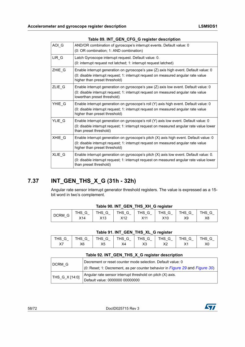
Accelerometer and gyroscope register description LSM9DS1
58/72 DocID025715 Rev 3
Table 89. INT_GEN_CFG_G register description
7.37 INT_GEN_THS_X_G (31h - 32h)
Angular rate sensor interrupt generator threshold registers. The value is expressed as a 15-bit word in two’s complement.
Table 92. INT_GEN_THS_X_G register description
AOI_G AND/OR combination of gyroscope’s interrupt events. Default value: 0
(0: OR combination; 1: AND combination)
LIR_G Latch Gyroscope interrupt request. Default value: 0.
(0: interrupt request not latched; 1: interrupt request latched)
ZHIE_G Enable interrupt generation on gyroscope’s yaw (Z) axis high event. Default value: 0
(0: disable interrupt request; 1: interrupt request on measured angular rate value higher than preset threshold)
ZLIE_G Enable interrupt generation on gyroscope’s yaw (Z) axis low event. Default value: 0
(0: disable interrupt request; 1: interrupt request on measured angular rate value lowerthan preset threshold)
YHIE_G Enable interrupt generation on gyroscope’s roll (Y) axis high event. Default value: 0
(0: disable interrupt request; 1: interrupt request on measured angular rate value higher than preset threshold)
YLIE_G Enable interrupt generation on gyroscope’s roll (Y) axis low event. Default value: 0
(0: disable interrupt request; 1: interrupt request on measured angular rate value lower than preset threshold)
XHIE_G Enable interrupt generation on gyroscope’s pitch (X) axis high event. Default value: 0
(0: disable interrupt request; 1: interrupt request on measured angular rate value higher than preset threshold)
XLIE_G Enable interrupt generation on gyroscope’s pitch (X) axis low event. Default value: 0.
(0: disable interrupt request; 1: interrupt request on measured angular rate value lower than preset threshold)
Table 90. INT_GEN_THS_XH_G register
DCRM_GTHS_G_
X14
THS_G_
X13
THS_G_
X12
THS_G_
X11
THS_G_
X10
THS_G_
X9
THS_G_
X8
Table 91. INT_GEN_THS_XL_G register
THS_G_
X7
THS_G_
X6
THS_G_
X5
THS_G_
X4
THS_G_
X3
THS_G_
X2
THS_G_
X1
THS_G_
X0
DCRM_GDecrement or reset counter mode selection. Default value: 0
(0: Reset; 1: Decrement, as per counter behavior in Figure 29 and Figure 30)
THS_G_X [14:0]Angular rate sensor interrupt threshold on pitch (X) axis.
Default value: 0000000 00000000
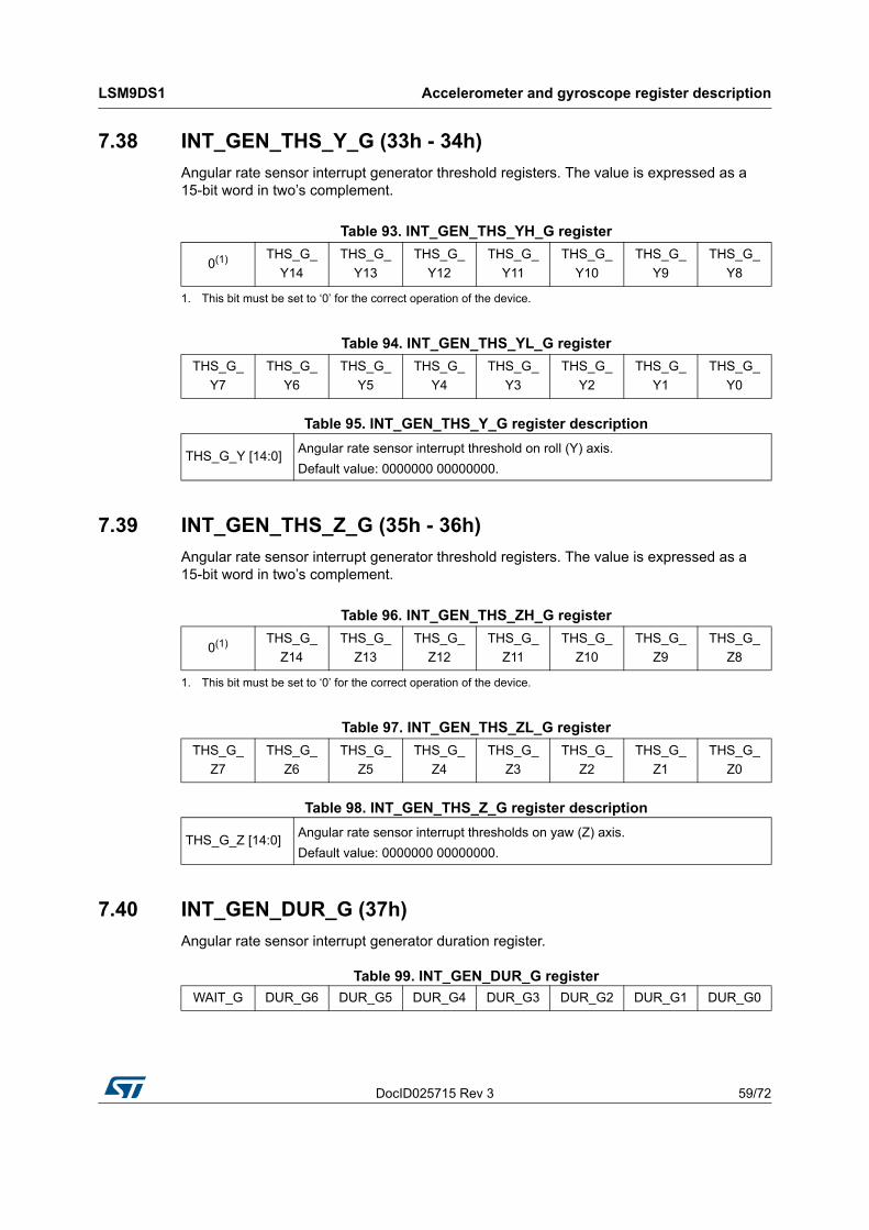
DocID025715 Rev 3 59/72
LSM9DS1 Accelerometer and gyroscope register description
72
7.38 INT_GEN_THS_Y_G (33h - 34h)
Angular rate sensor interrupt generator threshold registers. The value is expressed as a 15-bit word in two’s complement.
Table 95. INT_GEN_THS_Y_G register description
7.39 INT_GEN_THS_Z_G (35h - 36h)
Angular rate sensor interrupt generator threshold registers. The value is expressed as a 15-bit word in two’s complement.
Table 98. INT_GEN_THS_Z_G register description
7.40 INT_GEN_DUR_G (37h)
Angular rate sensor interrupt generator duration register.
Table 99. INT_GEN_DUR_G register
Table 93. INT_GEN_THS_YH_G register
0(1)
1. This bit must be set to ‘0’ for the correct operation of the device.
THS_G_
Y14
THS_G_
Y13
THS_G_
Y12
THS_G_
Y11
THS_G_
Y10
THS_G_
Y9
THS_G_
Y8
Table 94. INT_GEN_THS_YL_G register
THS_G_
Y7
THS_G_
Y6
THS_G_
Y5
THS_G_
Y4
THS_G_
Y3
THS_G_
Y2
THS_G_
Y1
THS_G_
Y0
THS_G_Y [14:0]Angular rate sensor interrupt threshold on roll (Y) axis.
Default value: 0000000 00000000.
Table 96. INT_GEN_THS_ZH_G register
0(1)
1. This bit must be set to ‘0’ for the correct operation of the device.
THS_G_
Z14
THS_G_
Z13
THS_G_
Z12
THS_G_
Z11
THS_G_
Z10
THS_G_
Z9
THS_G_
Z8
Table 97. INT_GEN_THS_ZL_G register
THS_G_
Z7
THS_G_
Z6
THS_G_
Z5
THS_G_
Z4
THS_G_
Z3
THS_G_
Z2
THS_G_
Z1
THS_G_
Z0
THS_G_Z [14:0]Angular rate sensor interrupt thresholds on yaw (Z) axis.
Default value: 0000000 00000000.
WAIT_G DUR_G6 DUR_G5 DUR_G4 DUR_G3 DUR_G2 DUR_G1 DUR_G0

Accelerometer and gyroscope register description LSM9DS1
60/72 DocID025715 Rev 3
Table 100. INT_GEN_DUR_G register description
The DUR_G [6:0] bits set the minimum duration of the interrupt event to be recognized.Duration steps and maximum values depend on the ODR chosen.
The WAIT_G bit has the following meaning:
‘0’: the interrupt falls immediately if the signal crosses the selected threshold
‘1’: if the signal crosses the selected threshold, the interrupt falls after a number of samples equal to the value of the duration counter register.
For further details refer to Figure 29 and Figure 30.
Figure 29. Wait bit disabled
WAIT_G Exit from interrupt wait function enable. Default value: 0
(0: wait function off; 1: wait for DUR_G [6:0] samples before exiting interrupt)
DUR_G [6:0] Enter/exit interrupt duration value. Default Value: 000 0000

DocID025715 Rev 3 61/72
LSM9DS1 Accelerometer and gyroscope register description
72
Figure 30. Wait bit enabled

Magnetometer register description LSM9DS1
62/72 DocID025715 Rev 3
8 Magnetometer register description
8.1 OFFSET_X_REG_L_M (05h), OFFSET_X_REG_H_M (06h)
This register is a 16-bit register and represents the X offset used to compensate environmental effects (data is expressed as two’s complement). This value acts on the magnetic output data value in order to subtract the environmental offset.
Default value: 0
8.2 OFFSET_Y_REG_L_M (07h), OFFSET_Y_REG_H_M (08h)
This register is a 16-bit register and represents the Y offset used to compensate environmental effects (data is expressed as two’s complement). This value acts on the magnetic output data value in order to subtract the environmental offset.
Default value: 0
8.3 OFFSET_Z_REG_L_M (09h), OFFSET_Z_REG_H_M (0Ah)
This register is a 16-bit register and represents the Z offset used to compensate environmental effects (data is expressed as two’s complement). This value acts on the magnetic output data value in order to subtract the environmental offset.
Default value: 0.
Table 101. OFFSET_X_REG_L_M register
OFXM7 OFXM6 OFXM5 OFXM4 OFXM3 OFXM2 OFXM1 OFXM0
Table 102. OFFSET_X_REG_H_M register
OFXM15 OFXM14 OFXM13 OFXM12 OFXM11 OFXM10 OFXM9 OFXM8
Table 103. OFFSET_Y_REG_L_M register
OFYM7 OFYM6 OFYM5 OFYM4 OFYM3 OFYM2 OFYM1 OFYM0
Table 104. OFFSET_Y_REG_H_M register
OFYM15 OFYM14 OFYM13 OFYM12 OFYM11 OFYM10 OFYM9 OFYM8
Table 105. OFFSET_Z_REG_L_M register
OFZM7 OFZM6 OFZM5 OFZM4 OFZM3 OFZM2 OFZM1 OFZM0
Table 106. OFFSET_Z_REG_H_M register
OFZM15 OFZM14 OFZM13 OFZM12 OFZM11 OFZM10 OFZM9 OFZM8

DocID025715 Rev 3 63/72
LSM9DS1 Magnetometer register description
72
8.4 WHO_AM_I_M (0Fh)
Device identification register.
8.5 CTRL_REG1_M (20h)
Table 110. X and Y axes operative mode selection
Table 111. Output data rate configuration
Table 107. WHO_AM_I_M register
0 0 1 1 1 1 0 1
Table 108. CTRL_REG1_M registerTEMP_COMP
OM1 OM0 DO2 DO1 DO0 FAST_ODR ST
Table 109. CTRL_REG1_M register description
TEMP_COMP Temperature compensation enable. Default value: 0(0: temperature compensation disabled; 1: temperature compensation enabled)
OM[1:0]X and Y axes operative mode selection. Default value: 00(Refer to Table 110)
DO[2:0]Output data rate selection. Default value: 100
(Refer to Table 111)
FAST_ODRFAST_ODR enables data rates higher than 80 Hz. Default value: 0
(0: Fast_ODR disabled; 1: FAST_ODR enabled)
ST Self-test enable. Default value: 0(0: self-test disabled; 1: self-test enabled)
OM1 OM0 Operative mode for X and Y axes
0 0 Low-power mode
0 1 Medium-performance mode
1 0 High-performance mode
1 1 Ultra-high performance mode
DO2 DO1 DO0 ODR [Hz]
0 0 0 0.625
0 0 1 1.25
0 1 0 2.5
0 1 1 5
1 0 0 10
1 0 1 20
1 1 0 40
1 1 1 80

Magnetometer register description LSM9DS1
64/72 DocID025715 Rev 3
8.6 CTRL_REG2_M (21h)
8.7 CTRL_REG3_M (22h)
Table 112. CTRL_REG2_M register
0(1)
1. These bits must be set to ‘0’ for the correct operation of the device.
FS1 FS0 0(1) REBOOT SOFT_RST 0(1) 0(1)
Table 113. CTRL_REG2_M register description
FS[1:0] Full-scale configuration. Default value: 00Refer to Table 114
REBOOTReboot memory content. Default value: 0 (0: normal mode; 1: reboot memory content)
SOFT_RSTConfiguration registers and user register reset function.
(0: default value; 1: reset operation)
Table 114. Full-scale selection
FS1 FS0 Full scale
0 0 ± 4 gauss
0 1 ± 8 gauss
1 0 ± 12 gauss
1 1 ± 16 gauss
Table 115. CTRL_REG3_M register
I2C_DISABLE
0(1)
1. These bits must be set to ‘0’ for the correct operation of the device.
LP 0(1) 0(1) SIM MD1 MD0
Table 116. CTRL_REG3_M register description
I2C_DISABLE Disable I2C interface. Default value 0. (0: I2C enable; 1: I2C disable)
LP Low-power mode configuration. Default value: 0If this bit is ‘1’, the DO[2:0] is set to 0.625 Hz and the system performs, for each channel, the minimum number of averages. Once the bit is set to ‘0’, the magnetic data rate is configured by the DO bits in the CTRL_REG1_M (20h) register.
SIM SPI Serial Interface mode selection. Default value: 0(0: SPI only write operations enabled; 1: SPI read and write operations enable).
MD[1:0] Operating mode selection. Default value: 11Refer to Table 117.

DocID025715 Rev 3 65/72
LSM9DS1 Magnetometer register description
72
Table 117. System operating mode selection
8.8 CTRL_REG4_M (23h)
Table 120. Z-axis operative mode selection
8.9 CTRL_REG5_M (24h)
MD1 MD0 Mode
0 0 Continuous-conversion mode
0 1 Single-conversion mode
1 0 Power-down mode
1 1 Power-down mode
Table 118. CTRL_REG4_M register
0(1)
1. These bits must be set to ‘0’ for the correct operation of the device
0(1) 0(1) 0(1) OMZ1 OMZ0 BLE 0(1)
Table 119. CTRL_REG4_M register description
OMZ[1:0] Z-axis operative mode selection. Default value: 00. Refer to Table 120.
BLE Big/Little Endian data selection. Default value: 0 (0: data LSb at lower address; 1: data MSb at lower address)
OMZ1 OMZ0 Operative mode for Z-axis
0 0 Low-power mode
0 1 Medium-performance mode
1 0 High-performance mode
1 1 Ultra-high performance mode
Table 121. CTRL_REG5_M register
FAST_READ BDU 0(1)
1. These bits must be set to ‘0’ for the correct operation of the device.
0(1) 0(1) 0(1) 0(1) 0(1)
Table 122. CTRL_REG5_M register description
FAST_READ FAST_READ allows reading the high part of DATA OUT only in order to increasereading efficiency. Default value: 0(0: FAST_READ disabled; 1: FAST_READ enabled)
BDU Block data update for magnetic data. Default value: 0(0: continuous update; 1: output registers not updated until MSB and LSB have been read)

Magnetometer register description LSM9DS1
66/72 DocID025715 Rev 3
8.10 STATUS_REG_M (27h)
8.11 OUT_X_L_M (28h), OUT_X_H_M(29h)
Magnetometer X-axis data output. The value of the magnetic field is expressed as two’s complement.
8.12 OUT_Y_L_M (2Ah), OUT_Y_H_M (2Bh)
Magnetometer Y-axis data output. The value of the magnetic field is expressed as two’s complement.
8.13 OUT_Z_L_M (2Ch), OUT_Z_H_M (2Dh)
Magnetometer Z-axis data output. The value of the magnetic field is expressed as two’s complement.
Table 123. STATUS_REG_M register
ZYXOR ZOR YOR XOR ZYXDA ZDA YDA XDA
Table 124. STATUS_REG_M register description
ZYXOR X, Y and Z-axis data overrun. Default value: 0(0: no overrun has occurred; 1: a new set of data has overwritten the previous set)
ZOR Z-axis data overrun. Default value: 0(0: no overrun has occurred; 1: new data for the Z-axis has overwritten the previous data)
YOR Y-axis data overrun. Default value: 0(0: no overrun has occurred; 1: new data for the Y-axis has overwritten the previous data)
XOR X-axis data overrun. Default value: 0(0: no overrun has occurred; 1: new data for the X-axis has overwritten the previous data)
ZYXDA X, Y and Z-axis new data available. Default value: 0(0: a new set of data is not yet available; 1: a new set of data is available)
ZDA Z-axis new data available. Default value: 0(0: new data for the Z-axis is not yet available; 1: new data for the Z-axis is available)
YDA Y-axis new data available. Default value: 0(0: new data for the Y-axis is not yet available; 1: new data for the Y-axis is available)
XDA X-axis new data available. Default value: 0(0: a new data for the X-axis is not yet available; 1: a new data for the X-axis is available)
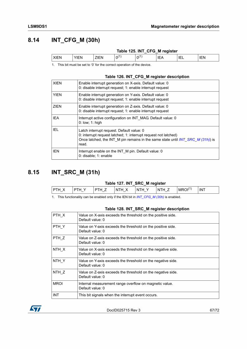
DocID025715 Rev 3 67/72
LSM9DS1 Magnetometer register description
72
8.14 INT_CFG_M (30h)
8.15 INT_SRC_M (31h)
Table 125. INT_CFG_M register
XIEN YIEN ZIEN 0(1)
1. This bit must be set to ‘0’ for the correct operation of the device.
0(1) IEA IEL IEN
Table 126. INT_CFG_M register description
XIEN Enable interrupt generation on X-axis. Default value: 0 0: disable interrupt request; 1: enable interrupt request
YIEN Enable interrupt generation on Y-axis. Default value: 0 0: disable interrupt request; 1: enable interrupt request
ZIEN Enable interrupt generation on Z-axis. Default value: 0 0: disable interrupt request; 1: enable interrupt request
IEA Interrupt active configuration on INT_MAG. Default value: 00: low; 1: high
IEL Latch interrupt request. Default value: 00: interrupt request latched; 1: interrupt request not latched)Once latched, the INT_M pin remains in the same state until INT_SRC_M (31h)) is read.
IEN Interrupt enable on the INT_M pin. Default value: 0 0: disable; 1: enable
Table 127. INT_SRC_M register
PTH_X PTH_Y PTH_Z NTH_X NTH_Y NTH_Z MROI(1)
1. This functionality can be enabled only if the IEN bit in INT_CFG_M (30h) is enabled.
INT
Table 128. INT_SRC_M register description
PTH_X Value on X-axis exceeds the threshold on the positive side. Default value: 0
PTH_Y Value on Y-axis exceeds the threshold on the positive side. Default value: 0
PTH_Z Value on Z-axis exceeds the threshold on the positive side. Default value: 0
NTH_X Value on X-axis exceeds the threshold on the negative side. Default value: 0
NTH_Y Value on Y-axis exceeds the threshold on the negative side. Default value: 0
NTH_Z Value on Z-axis exceeds the threshold on the negative side. Default value: 0
MROI Internal measurement range overflow on magnetic value. Default value: 0
INT This bit signals when the interrupt event occurs.

Magnetometer register description LSM9DS1
68/72 DocID025715 Rev 3
8.16 INT_THS_L(32h), INT_THS_H(33h)
Interrupt threshold. Default value: 0.
The value is expressed in 15-bit unsigned.
Even if the threshold is expressed in absolute value, the device detects both positive and negative thresholds.
Table 129. INT_THS_L_M register
THS7 THS6 THS5 THS4 THS3 THS2 THS1 THS0
Table 130. INT_THS_H_M register
0(1)
1. This bit must be set to ‘0’ for the correct operation of the device.
THS14 THS13 THS12 THS11 THS10 THS9 THS8

DocID025715 Rev 3 69/72
LSM9DS1 Package information
72
9 Package information
In order to meet environmental requirements, ST offers these devices in different grades ofECOPACK® packages, depending on their level of environmental compliance. ECOPACK®
specifications, grade definitions and product status are available at: www.st.com. ECOPACK is an ST trademark.
9.1 Soldering information
The LGA package is compliant with the ECOPACK®, RoHS and “Green” standard. It is qualified for soldering heat resistance according to JEDEC J-STD-020.
Leave “Pin 1 Indicator” unconnected during soldering.
Land pattern and soldering recommendations are available at www.st.com/mems.
9.2 LGA package information
Figure 31. LGA (3.5x3x1 mm) 24-lead package outline

Package information LSM9DS1
70/72 DocID025715 Rev 3
Table 131. LGA (3.5x3x1 mm) 24-lead package mechanical data
Dim.mm
Min. Typ. Max.
A1 1.000 1.027
A3 0.130
D1 2.850 3.000 3.150
E1 3.350 3.500 3.650
L1 2.960 3.010 3.060
L2 1.240 1.290 1.340
N1 0.165 0.215 0.265
P2 0.200 0.250 0.300
a 45°
T1 0.300 0.350 0.400
T2 0.180 0.230 0.280
K 0.050
M 0.100

DocID025715 Rev 3 71/72
LSM9DS1 Revision history
72
10 Revision history
Table 132. Document revision history
Date Revision Changes
18-Dec-2013 1 Initial release
05-Nov-2014 2
Datasheet status promoted from preliminary to production data
Added ±16 g linear acceleration full scale throughout datasheet
Corrected typo in footnote 3, 4 and 5 of Table 2: Pin description
Updated Figure 15: LSM9DS1 electrical connections and Section 4.1: External capacitors
Updated Table 117: System operating mode selection
12-Mar-2015 3Added FAST_ODR bit to CTRL_REG1_M (20h)
Added FAST_READ bit to CTRL_REG5_M (24h)

LSM9DS1
72/72 DocID025715 Rev 3
IMPORTANT NOTICE – PLEASE READ CAREFULLY
STMicroelectronics NV and its subsidiaries (“ST”) reserve the right to make changes, corrections, enhancements, modifications, and improvements to ST products and/or to this document at any time without notice. Purchasers should obtain the latest relevant information on ST products before placing orders. ST products are sold pursuant to ST’s terms and conditions of sale in place at the time of order acknowledgement.
Purchasers are solely responsible for the choice, selection, and use of ST products and ST assumes no liability for application assistance or the design of Purchasers’ products.
No license, express or implied, to any intellectual property right is granted by ST herein.
Resale of ST products with provisions different from the information set forth herein shall void any warranty granted by ST for such product.
ST and the ST logo are trademarks of ST. All other product or service names are the property of their respective owners.
Information in this document supersedes and replaces information previously supplied in any prior versions of this document.
© 2015 STMicroelectronics – All rights reserved