
Inductive Linear Position Sensing Booster Pack (Rev. A)
28
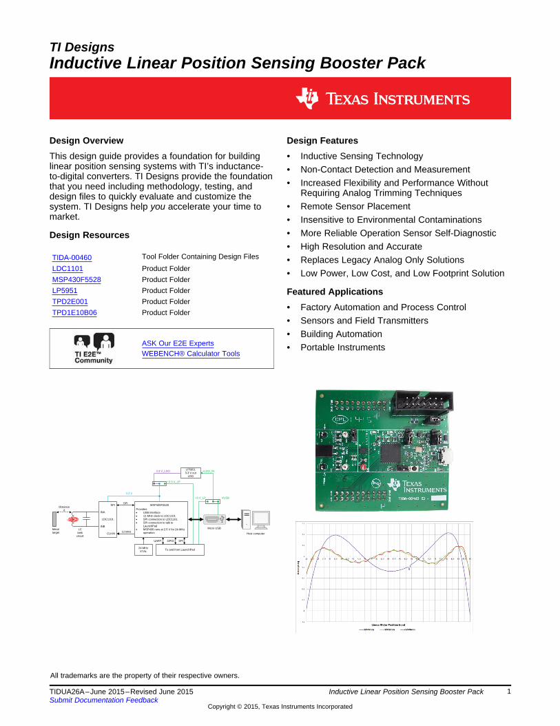
INA SPI INB CLKIN LDC1101 Provides: N USB interface N 12-MHz clock to LDC1101 N SPI connection to LDC1101 N SPI connection to talk to LaunchPad N MSP430 runs at 2.5 V for 24-MHz operation MSP430F5528 SPI 12 MHz Distance d Metal target LC tank circuit 24-MHz XTAL To and from LaunchPad LP5951 3.3 V out LDO UART GPIO SPI 3.3 V +3.3 V_LP Micro USB +5 V_LP VUSB +LDO_IN 3.3 V_LDO Host computer TI Designs Inductive Linear Position Sensing Booster Pack Design Overview Design Features This design guide provides a foundation for building • Inductive Sensing Technology linear position sensing systems with TI’s inductance- • Non-Contact Detection and Measurement to-digital converters. TI Designs provide the foundation • Increased Flexibility and Performance Without that you need including methodology, testing, and Requiring Analog Trimming Techniques design files to quickly evaluate and customize the • Remote Sensor Placement system. TI Designs help you accelerate your time to market. • Insensitive to Environmental Contaminations • More Reliable Operation Sensor Self-Diagnostic Design Resources • High Resolution and Accurate Tool Folder Containing Design Files TIDA-00460 • Replaces Legacy Analog Only Solutions LDC1101 Product Folder • Low Power, Low Cost, and Low Footprint Solution MSP430F5528 Product Folder LP5951 Product Folder Featured Applications TPD2E001 Product Folder • Factory Automation and Process Control TPD1E10B06 Product Folder • Sensors and Field Transmitters • Building Automation ASK Our E2E Experts • Portable Instruments WEBENCH® Calculator Tools All trademarks are the property of their respective owners. 1 TIDUA26A – June 2015 – Revised June 2015 Inductive Linear Position Sensing Booster Pack Submit Documentation Feedback Copyright © 2015, Texas Instruments Incorporated
Transcript of Inductive Linear Position Sensing Booster Pack (Rev. A)
INA
SPI
INB
CLKIN
LDC1101
Provides:x USB interfacex 12-MHz clock to LDC1101x SPI connection to LDC1101x SPI connection to talk to
LaunchPadx MSP430 runs at 2.5 V for 24-MHz
operation
MSP430F5528SPI
12 MHz
Distance d
Metal target
LC tank
circuit
24-MHzXTAL
To and from LaunchPad
LP59513.3 V out
LDO
UART GPIO SPI
3.3 V
+3.3 V_LP
Micro USB
+5 V_LP VUSB
+LDO_IN3.3 V_LDO
Host computer
TI DesignsInductive Linear Position Sensing Booster Pack
Design Overview Design FeaturesThis design guide provides a foundation for building • Inductive Sensing Technologylinear position sensing systems with TI’s inductance- • Non-Contact Detection and Measurementto-digital converters. TI Designs provide the foundation
• Increased Flexibility and Performance Withoutthat you need including methodology, testing, andRequiring Analog Trimming Techniquesdesign files to quickly evaluate and customize the
• Remote Sensor Placementsystem. TI Designs help you accelerate your time tomarket. • Insensitive to Environmental Contaminations
• More Reliable Operation Sensor Self-DiagnosticDesign Resources• High Resolution and Accurate
Tool Folder Containing Design FilesTIDA-00460 • Replaces Legacy Analog Only SolutionsLDC1101 Product Folder • Low Power, Low Cost, and Low Footprint SolutionMSP430F5528 Product FolderLP5951 Product Folder Featured ApplicationsTPD2E001 Product Folder
• Factory Automation and Process ControlTPD1E10B06 Product Folder• Sensors and Field Transmitters• Building Automation
ASK Our E2E Experts • Portable InstrumentsWEBENCH® Calculator Tools
All trademarks are the property of their respective owners.
1TIDUA26A–June 2015–Revised June 2015 Inductive Linear Position Sensing Booster PackSubmit Documentation Feedback
Copyright © 2015, Texas Instruments Incorporated
Key System Specifications www.ti.com
An IMPORTANT NOTICE at the end of this TI reference design addresses authorized use, intellectual property matters and otherimportant disclaimers and information.
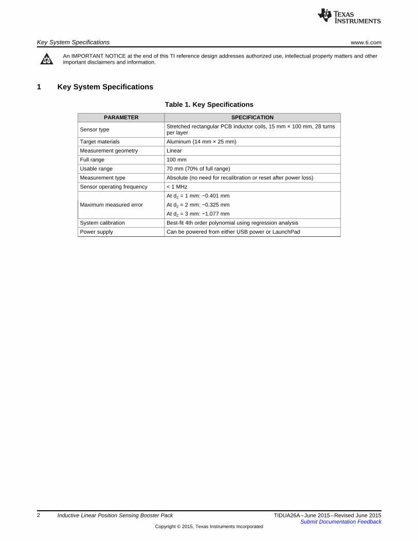
1 Key System Specifications
Table 1. Key Specifications
PARAMETER SPECIFICATIONStretched rectangular PCB inductor coils, 15 mm × 100 mm, 28 turnsSensor type per layer
Target materials Aluminum (14 mm × 25 mm)Measurement geometry LinearFull range 100 mmUsable range 70 mm (70% of full range)Measurement type Absolute (no need for recalibration or reset after power loss)Sensor operating frequency < 1 MHz
At dZ = 1 mm: −0.401 mmMaximum measured error At dZ = 2 mm: −0.325 mm
At dZ = 3 mm: −1.077 mmSystem calibration Best-fit 4th order polynomial using regression analysisPower supply Can be powered from either USB power or LaunchPad
2 Inductive Linear Position Sensing Booster Pack TIDUA26A–June 2015–Revised June 2015Submit Documentation Feedback
Copyright © 2015, Texas Instruments Incorporated

www.ti.com System Description
2 System DescriptionIn all automated factory floor applications, sensors are necessary to provide the programmable logiccontroller (PLC) with information. The sensors supply the necessary signals for positions and limits, orserve as pulse pick-ups for counting tasks or for monitoring rotational speed. Even the best controllerscannot control the process without reliable sensors. When accurately measuring the distance less that isless than a few inches is necessary and the application calls for metal sensing, then the inductive sensorprovides the required sensing solution. The inductive sensing technology solution seems to be a naturalchoice due its contactless, magnet-free sensing, contamination-resistant, and maintenance free operation.Additionally, inductive sensing technology is suitable for use in harsh environments because vibration,dust, dirt, oil, and moisture do not hinder the performance. Inductive sensors detect all ferrous metalswithout contact, which means no wear and tear.
The technology of inductive sensing has been around for decades. Additionally, the inductive sensor iscurrently the best-selling sensing technology worldwide, indicating a well-proven solution over a period ofdecades in long-term industrial use. Historically, this technique has required complex, analog-onlycircuitry, making it a costly technique for applications outside of industrial controls or portable metaldetectors.
Typical implementations of distance measurements use expensive rare-earth magnets. To lower theoverall system cost, this reference design describes the implementation of the industry’s first inductance-to-digital converters from TI for linear position sensing without the use of any expensive rare-earthmagnets. Linear position sensing determines the position of a target that moves laterally across aninductive sensor that is generating a magnetic field. An inductance-to-digital converter (LDC), such as anLDC1000 or LDC1101 device, senses the inductance changes of an inductor that comes into proximitywith a conductive target, such as a piece of metal. The LDC measures this inductance shift to provideinformation about the position of a conductive target over a sensor coil. The inductance shift is caused byeddy currents generated in the target due to the magnetic field of the sensor. These eddy currentsgenerate a secondary magnetic field that opposes the sensor field, causing a shift in the observedinductance (see Section 4 for a more detailed explanation).
There are two approaches to implement a linear position sensing system with an inductance-to-digitalconverter (LDC). Both approaches utilize a PCB coil as a sensor.1. A circular coil can be used to detect the position of a triangular conductive target.2. A stretched coil design that produces a non-homogeneous AC magnetic field can be used to determine
the position of a rectangular conductive target.
The intention of this reference design is to mainly focus on the second approach and provide a head-startadvantage to system designers for integrating TI’s family of inductance-to-digital converters into newapplications that require high-resolution linear position sensing. The following lists the overall system-levelchallenges for this design:• Proper sensor coil design to achieve desired measurement resolution• Proper conversion• Calibration of inductance-to-digital converter output into usable data• Testing
3TIDUA26A–June 2015–Revised June 2015 Inductive Linear Position Sensing Booster PackSubmit Documentation Feedback
Copyright © 2015, Texas Instruments Incorporated
RP + L
Meas
INA
INB
LDC1101VDD
Registers
+ Logic
GND
SPI
CLKIN
SCLK
CSB
SDO
SDI
High Res
L Meas
Sensor
Driver
CLDO
Threshold
Compare
System Description www.ti.com
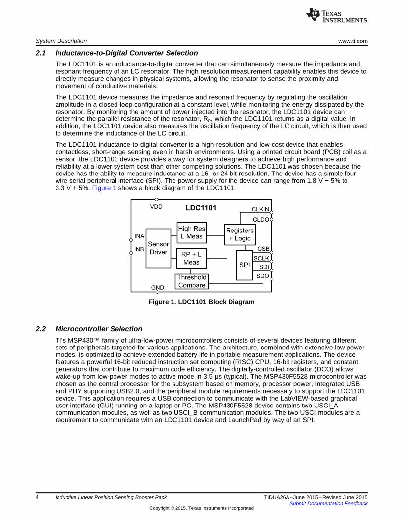
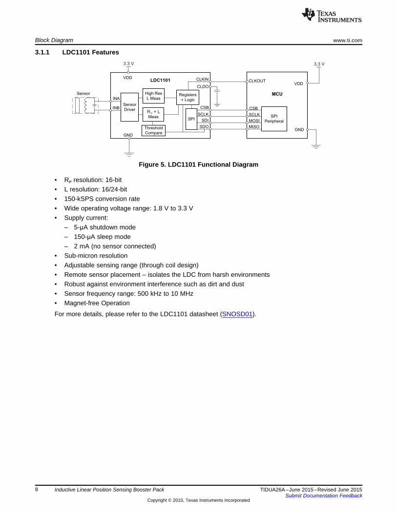
2.1 Inductance-to-Digital Converter SelectionThe LDC1101 is an inductance-to-digital converter that can simultaneously measure the impedance andresonant frequency of an LC resonator. The high resolution measurement capability enables this device todirectly measure changes in physical systems, allowing the resonator to sense the proximity andmovement of conductive materials.
The LDC1101 device measures the impedance and resonant frequency by regulating the oscillationamplitude in a closed-loop configuration at a constant level, while monitoring the energy dissipated by theresonator. By monitoring the amount of power injected into the resonator, the LDC1101 device candetermine the parallel resistance of the resonator, RP, which the LDC1101 returns as a digital value. Inaddition, the LDC1101 device also measures the oscillation frequency of the LC circuit, which is then usedto determine the inductance of the LC circuit.
The LDC1101 inductance-to-digital converter is a high-resolution and low-cost device that enablescontactless, short-range sensing even in harsh environments. Using a printed circuit board (PCB) coil as asensor, the LDC1101 device provides a way for system designers to achieve high performance andreliability at a lower system cost than other competing solutions. The LDC1101 was chosen because thedevice has the ability to measure inductance at a 16- or 24-bit resolution. The device has a simple four-wire serial peripheral interface (SPI). The power supply for the device can range from 1.8 V − 5% to3.3 V + 5%. Figure 1 shows a block diagram of the LDC1101.
Figure 1. LDC1101 Block Diagram
2.2 Microcontroller SelectionTI’s MSP430™ family of ultra-low-power microcontrollers consists of several devices featuring differentsets of peripherals targeted for various applications. The architecture, combined with extensive low powermodes, is optimized to achieve extended battery life in portable measurement applications. The devicefeatures a powerful 16-bit reduced instruction set computing (RISC) CPU, 16-bit registers, and constantgenerators that contribute to maximum code efficiency. The digitally-controlled oscillator (DCO) allowswake-up from low-power modes to active mode in 3.5 μs (typical). The MSP430F5528 microcontroller waschosen as the central processor for the subsystem based on memory, processor power, integrated USBand PHY supporting USB2.0, and the peripheral module requirements necessary to support the LDC1101device. This application requires a USB connection to communicate with the LabVIEW-based graphicaluser interface (GUI) running on a laptop or PC. The MSP430F5528 device contains two USCI_Acommunication modules, as well as two USCI_B communication modules. The two USCI modules are arequirement to communicate with an LDC1101 device and LaunchPad by way of an SPI.
4 Inductive Linear Position Sensing Booster Pack TIDUA26A–June 2015–Revised June 2015Submit Documentation Feedback
Copyright © 2015, Texas Instruments Incorporated
www.ti.com System Description
2.3 Power ManagementThe LP5951 low-dropout (LDO) regulator devices were chosen as the power management devices for thesubsystem for several reasons. The first reason is that this particular subsystem is designed to work froma nominal input voltage of 3.3 V or 5 V (from a LaunchPad or 5-V USB). The LP5951 device has a currentlimit of 150 mA and an adjustable output voltage range from 1.3 V to 3.7 V at a low quiescent current of29 µA (typical), which is significantly higher than the anticipated, maximum total operating load of thesubsystem. Only one LP5951 device is used in this subsystem, to regulate a 3.3-V output for theMSP430F5528 and LDC1101 devices.
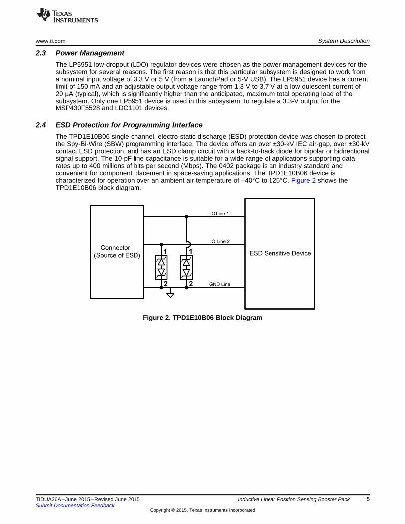
2.4 ESD Protection for Programming InterfaceThe TPD1E10B06 single-channel, electro-static discharge (ESD) protection device was chosen to protectthe Spy-Bi-Wire (SBW) programming interface. The device offers an over ±30-kV IEC air-gap, over ±30-kVcontact ESD protection, and has an ESD clamp circuit with a back-to-back diode for bipolar or bidirectionalsignal support. The 10-pF line capacitance is suitable for a wide range of applications supporting datarates up to 400 millions of bits per second (Mbps). The 0402 package is an industry standard andconvenient for component placement in space-saving applications. The TPD1E10B06 device ischaracterized for operation over an ambient air temperature of –40°C to 125°C. Figure 2 shows theTPD1E10B06 block diagram.
Figure 2. TPD1E10B06 Block Diagram
5TIDUA26A–June 2015–Revised June 2015 Inductive Linear Position Sensing Booster PackSubmit Documentation Feedback
Copyright © 2015, Texas Instruments Incorporated
0.1 µF
USB
Controller
RT
RT
VBUS
D+
D–
GND
GND
IO2
D1
IO1
VCC
System Description www.ti.com
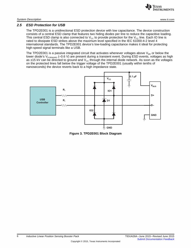
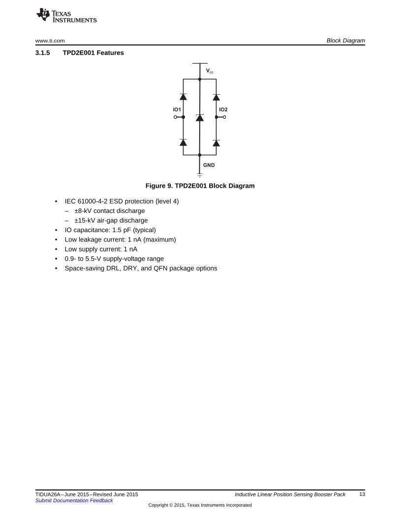
2.5 ESD Protection for USBThe TPD2E001 is a unidirectional ESD protection device with low capacitance. The device constructionconsists of a central ESD clamp that features two hiding diodes per line to reduce the capacitive loading.This central ESD clamp is also connected to VCC to provide protection for the VCC line. Each IO line israted to dissipate ESD strikes above the maximum level specified in the IEC 61000-4-2 level 4international standards. The TPD2E001 device’s low-loading capacitance makes it ideal for protectinghigh-speed signal terminals like a USB.
The TPD2E001 is a passive integrated circuit that activates whenever voltages above VBR or below thelower diode’s VFORWARD (–0.6 V) are present during a transient event. During ESD events, voltages as highas ±15 kV can be directed to ground and VCC through the internal diode network. As soon as the voltageson the protected lines fall below the trigger voltage of the TPD2E001 (usually within tenths ofnanoseconds) the device reverts back to a high impedance state.
Figure 3. TPD2E001 Block Diagram
6 Inductive Linear Position Sensing Booster Pack TIDUA26A–June 2015–Revised June 2015Submit Documentation Feedback
Copyright © 2015, Texas Instruments Incorporated
INA
SPI
INB
CLKIN
LDC1101
Provides:x USB interfacex 12-MHz clock to LDC1101x SPI connection to LDC1101x SPI connection to talk to
LaunchPadx MSP430 runs at 2.5 V for 24-MHz
operation
MSP430F5528SPI
12 MHz
Distance d
Metal target
LC tank
circuit
24-MHzXTAL
To and from LaunchPad
LP59513.3 V out
LDO
UART GPIO SPI
3.3 V
+3.3 V_LP
Micro USB
+5 V_LP VUSB
+LDO_IN3.3 V_LDO
Host computer
www.ti.com Block Diagram
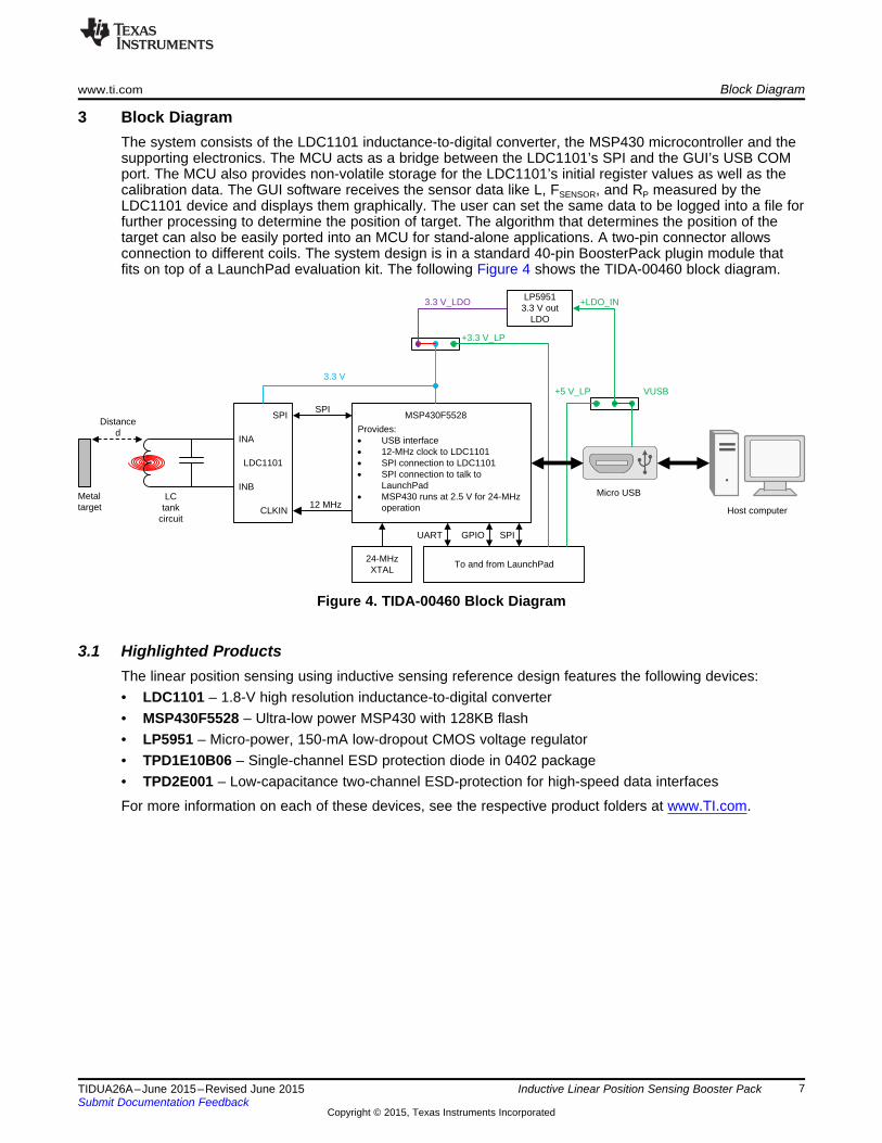
3 Block DiagramThe system consists of the LDC1101 inductance-to-digital converter, the MSP430 microcontroller and thesupporting electronics. The MCU acts as a bridge between the LDC1101’s SPI and the GUI’s USB COMport. The MCU also provides non-volatile storage for the LDC1101’s initial register values as well as thecalibration data. The GUI software receives the sensor data like L, FSENSOR, and RP measured by theLDC1101 device and displays them graphically. The user can set the same data to be logged into a file forfurther processing to determine the position of target. The algorithm that determines the position of thetarget can also be easily ported into an MCU for stand-alone applications. A two-pin connector allowsconnection to different coils. The system design is in a standard 40-pin BoosterPack plugin module thatfits on top of a LaunchPad evaluation kit. The following Figure 4 shows the TIDA-00460 block diagram.
Figure 4. TIDA-00460 Block Diagram
3.1 Highlighted ProductsThe linear position sensing using inductive sensing reference design features the following devices:• LDC1101 – 1.8-V high resolution inductance-to-digital converter• MSP430F5528 – Ultra-low power MSP430 with 128KB flash• LP5951 – Micro-power, 150-mA low-dropout CMOS voltage regulator• TPD1E10B06 – Single-channel ESD protection diode in 0402 package• TPD2E001 – Low-capacitance two-channel ESD-protection for high-speed data interfaces
For more information on each of these devices, see the respective product folders at www.TI.com.
7TIDUA26A–June 2015–Revised June 2015 Inductive Linear Position Sensing Booster PackSubmit Documentation Feedback
Copyright © 2015, Texas Instruments Incorporated
R + LP
3.3 V 3.3 V
Block Diagram www.ti.com
3.1.1 LDC1101 Features
Figure 5. LDC1101 Functional Diagram
• RP resolution: 16-bit• L resolution: 16/24-bit• 150-kSPS conversion rate• Wide operating voltage range: 1.8 V to 3.3 V• Supply current:
– 5-μA shutdown mode– 150-μA sleep mode– 2 mA (no sensor connected)
• Sub-micron resolution• Adjustable sensing range (through coil design)• Remote sensor placement – isolates the LDC from harsh environments• Robust against environment interference such as dirt and dust• Sensor frequency range: 500 kHz to 10 MHz• Magnet-free Operation
For more details, please refer to the LDC1101 datasheet (SNOSD01).
8 Inductive Linear Position Sensing Booster Pack TIDUA26A–June 2015–Revised June 2015Submit Documentation Feedback
Copyright © 2015, Texas Instruments Incorporated

UnifiedClock
System128KB96KB64KB32KB
Flash
8KB+2KB6KB+2KB4KB+2KB
RAM
MCLK
ACLK
SMCLK
I/O PortsP1/P2
2×8 I/OsInterrupt
& Wakeup
PA1×16 I/Os
CPUXV2and
WorkingRegisters
EEM(L: 8+2)
XIN XOUT
JTAG/
InterfaceSBW
PA PB PC PD
DMA
3 Channel
XT2IN
XT OUT2
PowerManagement
LDOSVM/Brownout
SVS
SYS
Watchdog
Port MapControl
(P4)
I/O PortsP3/P4
2×8 I/Os
PB1×16 I/Os
I/O PortsP5/P6
2×8 I/Os
PC1×16 I/Os
I/O PortsP7/P8
1×8 I/Os1
PD1×11 I/Os
×3 I/Os
Full-speedUSB
USB-PHYUSB-LDOUSB-PLL
MPY32
TA0
Timer_A5 CC
Registers
TA1
Timer_A3 CC
Registers
TB0
Timer_B7 CC
Registers
RTC_A CRC16
USCI0,1
USCI_Ax:UART,
IrDA, SPI
USCI_Bx:SPI, I2C
ADC12_A
200 KSPS
16 Channels(14 ext/2 int)
Autoscan
12 Bit
DVCC DVSS AVCC AVSSP1.x P2.x P3.x P4.x P5.x P6.x DP,DM,PUR
RST/NMI
TA2
Timer_A3 CC
Registers
REF
VCORE
MAB
MDB
P7.x P8.x
COMP_B
12 Channels
www.ti.com Block Diagram
3.1.2 MSP430F5528 Features
Figure 6. MSP430F5528 Functional Diagram
• Low supply-voltage range: 3.6 V down to 1.8 V• Ultra-low power consumption
– Active mode (AM):• All system clocks active• 290 μA/MHz at 8 MHz, 3.0 V, Flash program execution (typical)• 150 μA/MHz at 8 MHz, 3.0 V, RAM program execution (typical)
– Standby mode (LPM3):• Real-time clock with crystal, watchdog, and supply supervisor operational, full RAM retention,
fast wake-up:• 1.9 μA at 2.2 V, 2.1 μA at 3.0 V (typical)• Low-power oscillator (VLO), general-purpose counter, watchdog, and supply supervisor
operational, full RAM retention, fast wake-up: 1.4 μA at 3.0 V (typical)– Off mode (LPM4)
• Full RAM retention, supply supervisor operational, fast wake-up: 1.1 μA at 3.0 V (typical)– Shutdown mode (LPM4.5): 0.18 μA at 3.0 V (typical)
• Wake-up from standby mode in 3.5 μs (typical)• 16-bit RISC architecture, extended memory, up to 25-MHz system clock• Flexible power management system:
– Fully integrated LDO with programmable regulated core supply voltage– Supply voltage supervision, monitoring, and brownout
• Unified clock system– Frequency-locked loop (FLL) control loop for frequency stabilization– Low-power, low-frequency internal clock source (VLO)– Low-frequency trimmed internal reference source (REFO)– 32-kHz watch crystals (XT1)– High-frequency crystals (XY1)– High-frequency crystals up to 32 MHz (XT2)
9TIDUA26A–June 2015–Revised June 2015 Inductive Linear Position Sensing Booster PackSubmit Documentation Feedback
Copyright © 2015, Texas Instruments Incorporated

Block Diagram www.ti.com
• 16-bit timer TA0, Timer_A with five capture/compare registers• 16-bit timer TA1, Timer_A with three capture/compare registers• 16-bit timer TA2, Timer_A with three capture/compare registers• 16-bit timer TB0, Timer_B with seven capture/compare shadow registers• Two universal serial communication interfaces
– USCI_A0 and USCI_A1 each support:• Enhanced UART supports auto-baud rate detection• IrDA encoder and decoder• Synchronous SPI
– USCI_B0 and USCI_B1 each support:• I2C™• Synchronous SPI
• Full-speed USB– Integrated USB-PLL– Integrated 3.3- and 1.8-V USB power system– Integrated USB-PLL– Eight input, eight output endpoints
• 12-bit analog-to-digital converter (ADC), for MSP430F552x device family only) with internal reference,sample-and-hold, and auto-scan feature
• Comparator• Hardware multiplier supporting 32-bit operations• Serial on-board programming, no external programming voltage required• Three-channel internal direct memory access (DMA)• Basic Timer with real-time clock feature• For complete module descriptions, see the MSP430x5xx and MSP430x6xx Family User's Guide
(SLAU208).
10 Inductive Linear Position Sensing Booster Pack TIDUA26A–June 2015–Revised June 2015Submit Documentation Feedback
Copyright © 2015, Texas Instruments Incorporated
Enable
Controller
Bias
Generator
Over
Current and
Thermal
Protection
LDO Core
and
Reference
IN
OUT
GND
EN
www.ti.com Block Diagram
3.1.3 LP5951 Features
Figure 7. LP5951 Block Diagram
• Input voltage range: 1.8 V to 5.5 V• Output voltage range: 1.3 V to 3.7 V• Excellent line transient response: ±2 mV (typical)• Excellent power supply rejection ratio (PSRR): –60 dB at 1 kHz typical• Low quiescent current of 29 μA typical• Small SC70-5 and SOT-23-5 packages• Fast turn-on time of 30 μs (typical)• Typical < 1-nA quiescent current in shutdown• Ensured 150-mA output current• Logic controlled enable 0.4 V/0.9 V• Good load transient response of 50 mVpp (typical)• Thermal overload and short-circuit protection• −40°C to 125°C junction temperature range
11TIDUA26A–June 2015–Revised June 2015 Inductive Linear Position Sensing Booster PackSubmit Documentation Feedback
Copyright © 2015, Texas Instruments Incorporated
Block Diagram www.ti.com
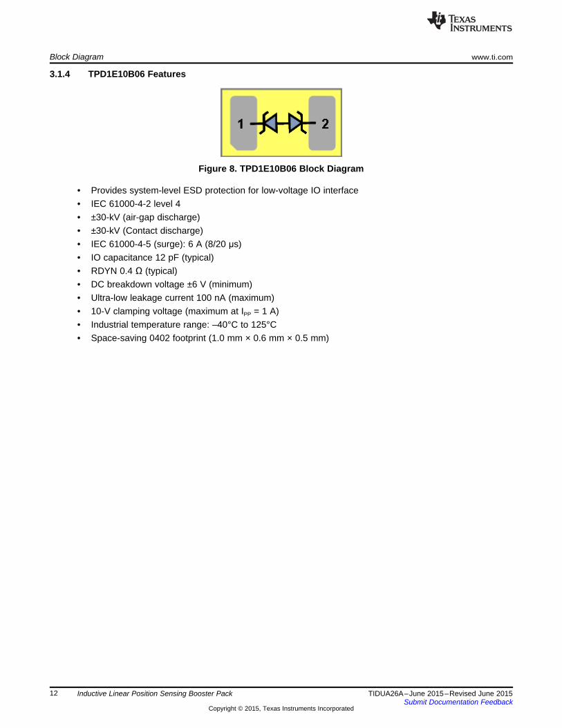
3.1.4 TPD1E10B06 Features
Figure 8. TPD1E10B06 Block Diagram
• Provides system-level ESD protection for low-voltage IO interface• IEC 61000-4-2 level 4• ±30-kV (air-gap discharge)• ±30-kV (Contact discharge)• IEC 61000-4-5 (surge): 6 A (8/20 μs)• IO capacitance 12 pF (typical)• RDYN 0.4 Ω (typical)• DC breakdown voltage ±6 V (minimum)• Ultra-low leakage current 100 nA (maximum)• 10-V clamping voltage (maximum at IPP = 1 A)• Industrial temperature range: –40°C to 125°C• Space-saving 0402 footprint (1.0 mm × 0.6 mm × 0.5 mm)
12 Inductive Linear Position Sensing Booster Pack TIDUA26A–June 2015–Revised June 2015Submit Documentation Feedback
Copyright © 2015, Texas Instruments Incorporated
IO2
GND
IO1
VCC
www.ti.com Block Diagram
3.1.5 TPD2E001 Features
Figure 9. TPD2E001 Block Diagram
• IEC 61000-4-2 ESD protection (level 4)– ±8-kV contact discharge– ±15-kV air-gap discharge
• IO capacitance: 1.5 pF (typical)• Low leakage current: 1 nA (maximum)• Low supply current: 1 nA• 0.9- to 5.5-V supply-voltage range• Space-saving DRL, DRY, and QFN package options
13TIDUA26A–June 2015–Revised June 2015 Inductive Linear Position Sensing Booster PackSubmit Documentation Feedback
Copyright © 2015, Texas Instruments Incorporated

Distance dTarget metal surface
Eddy currents
Conductance of metal
L s + L(d)
R s + R(d)
d
Metal Target
System Design Theory www.ti.com
4 System Design TheoryThe basic principle of inductive linear position sensing is related to the phenomenon of eddy currents.Walter Pepperl and Ludwig Fuchs first employed inductive sensing in 1958 in Mannheim, Germany. Theywanted to find a technology to replace mechanical contacts that would wear out in hostile environments orwere simply dangerous in explosive atmospheres due to arching. The basic principle of inductive sensingremains the same as Pepper and Fuchs’ original design.
An AC current flowing through a coil generates an AC magnetic field. If a user brings conductive materialinto the vicinity of the coil, such as a ferrous metal target, some of the energy from the oscillating magneticfield transfers to the metal target (see Figure 10). This transferred energy induces tiny circulating electricalcurrents known today as eddy currents on the surface of the target. The flowing eddy currents encounterelectrical resistance as they try to circulate, which creates a small amount of power loss in the form ofheat. These losses are known as eddy current losses. These eddy currents are a function of the distance,size, composition, and orientation of the target to the magnetic field. The induced eddy currents in themetal target then generate their own magnetic field (counter field or secondary field) that reacts with theoriginal field generated by the coil; this reaction changes the characteristics of the coil.
Figure 10. Inductor With Metal Target
This mechanism is best compared to a transformer, where the coil is the primary core and the eddycurrent is the secondary core. The inductive coupling between both cores depends on distance, shape,and the conductor’s characteristics. Hence, the resistance and inductance of the secondary core (eddycurrent), shows up as a distant, dependent resistive and inductive component on the primary side (coil).The following figures show a simplified circuit model. In Figure 11, the inductance LS is the coil’sinductance and RS is the coil’s parasitic series resistance. The inductance L(d), which is a function ofdistance d, is the coupled inductance of the metal target. Likewise, R(d) is the parasitic resistance of theeddy currents.
Figure 11. Metal Target Modeled as L and R With Circulating Eddy Currents
14 Inductive Linear Position Sensing Booster Pack TIDUA26A–June 2015–Revised June 2015Submit Documentation Feedback
Copyright © 2015, Texas Instruments Incorporated
+
–
Metaltarget
Sense coil
L
R
C
S
R
Demodulator
P
Gain control
V
V
REF
OUT
L s + L(d)
R s + R(d)
L s + L(d)
Oscillator
C C R p(d)
Oscillator
SP
S
L L(d)1R (d)
R R(d) C
æ ö +é ù= ç ÷ ê ú+ ë ûè ø
www.ti.com System Design Theory
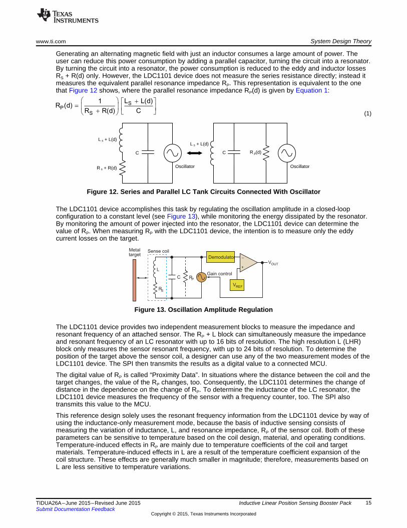
Generating an alternating magnetic field with just an inductor consumes a large amount of power. Theuser can reduce this power consumption by adding a parallel capacitor, turning the circuit into a resonator.By turning the circuit into a resonator, the power consumption is reduced to the eddy and inductor lossesRS + R(d) only. However, the LDC1101 device does not measure the series resistance directly; instead itmeasures the equivalent parallel resonance impedance RP. This representation is equivalent to the onethat Figure 12 shows, where the parallel resonance impedance RP(d) is given by Equation 1:
(1)
Figure 12. Series and Parallel LC Tank Circuits Connected With Oscillator
The LDC1101 device accomplishes this task by regulating the oscillation amplitude in a closed-loopconfiguration to a constant level (see Figure 13), while monitoring the energy dissipated by the resonator.By monitoring the amount of power injected into the resonator, the LDC1101 device can determine thevalue of RP. When measuring RP with the LDC1101 device, the intention is to measure only the eddycurrent losses on the target.
Figure 13. Oscillation Amplitude Regulation
The LDC1101 device provides two independent measurement blocks to measure the impedance andresonant frequency of an attached sensor. The RP + L block can simultaneously measure the impedanceand resonant frequency of an LC resonator with up to 16 bits of resolution. The high resolution L (LHR)block only measures the sensor resonant frequency, with up to 24 bits of resolution. To determine theposition of the target above the sensor coil, a designer can use any of the two measurement modes of theLDC1101 device. The SPI then transmits the results as a digital value to a connected MCU.
The digital value of RP is called “Proximity Data”. In situations where the distance between the coil and thetarget changes, the value of the RP changes, too. Consequently, the LDC1101 determines the change ofdistance in the dependence on the change of RP. To determine the inductance of the LC resonator, theLDC1101 device measures the frequency of the sensor with a frequency counter, too. The SPI alsotransmits this value to the MCU.
This reference design solely uses the resonant frequency information from the LDC1101 device by way ofusing the inductance-only measurement mode, because the basis of inductive sensing consists ofmeasuring the variation of inductance, L, and resonance impedance, RP of the sensor coil. Both of theseparameters can be sensitive to temperature based on the coil design, material, and operating conditions.Temperature-induced effects in RP are mainly due to temperature coefficients of the coil and targetmaterials. Temperature-induced effects in L are a result of the temperature coefficient expansion of thecoil structure. These effects are generally much smaller in magnitude; therefore, measurements based onL are less sensitive to temperature variations.
15TIDUA26A–June 2015–Revised June 2015 Inductive Linear Position Sensing Booster PackSubmit Documentation Feedback
Copyright © 2015, Texas Instruments Incorporated
TIDA-00460
System Design Theory www.ti.com
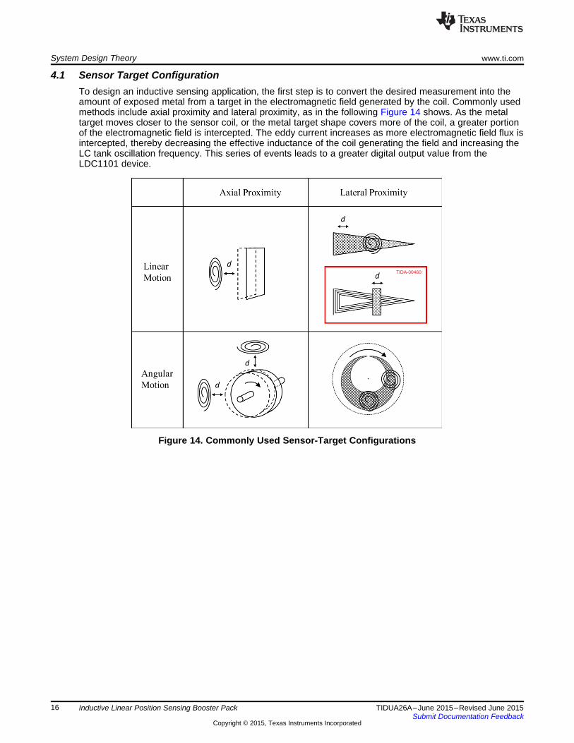
4.1 Sensor Target ConfigurationTo design an inductive sensing application, the first step is to convert the desired measurement into theamount of exposed metal from a target in the electromagnetic field generated by the coil. Commonly usedmethods include axial proximity and lateral proximity, as in the following Figure 14 shows. As the metaltarget moves closer to the sensor coil, or the metal target shape covers more of the coil, a greater portionof the electromagnetic field is intercepted. The eddy current increases as more electromagnetic field flux isintercepted, thereby decreasing the effective inductance of the coil generating the field and increasing theLC tank oscillation frequency. This series of events leads to a greater digital output value from theLDC1101 device.
Figure 14. Commonly Used Sensor-Target Configurations
16 Inductive Linear Position Sensing Booster Pack TIDUA26A–June 2015–Revised June 2015Submit Documentation Feedback
Copyright © 2015, Texas Instruments Incorporated
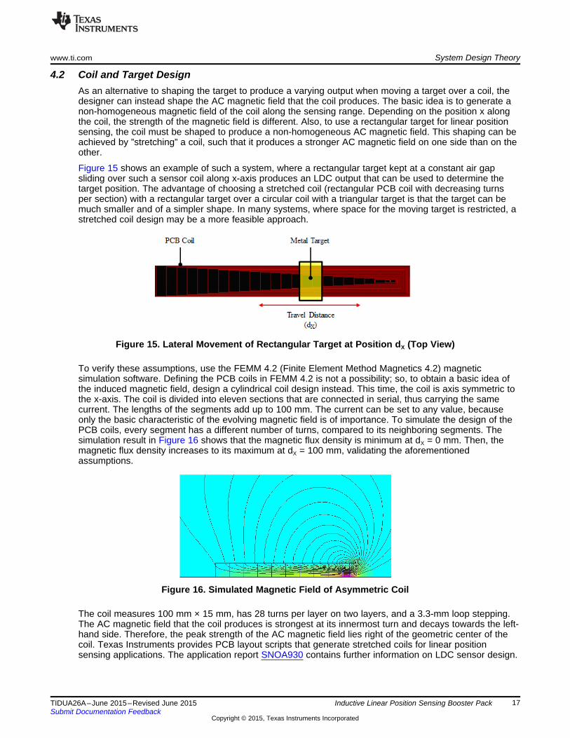
www.ti.com System Design Theory
4.2 Coil and Target DesignAs an alternative to shaping the target to produce a varying output when moving a target over a coil, thedesigner can instead shape the AC magnetic field that the coil produces. The basic idea is to generate anon-homogeneous magnetic field of the coil along the sensing range. Depending on the position x alongthe coil, the strength of the magnetic field is different. Also, to use a rectangular target for linear positionsensing, the coil must be shaped to produce a non-homogeneous AC magnetic field. This shaping can beachieved by ”stretching” a coil, such that it produces a stronger AC magnetic field on one side than on theother.
Figure 15 shows an example of such a system, where a rectangular target kept at a constant air gapsliding over such a sensor coil along x-axis produces an LDC output that can be used to determine thetarget position. The advantage of choosing a stretched coil (rectangular PCB coil with decreasing turnsper section) with a rectangular target over a circular coil with a triangular target is that the target can bemuch smaller and of a simpler shape. In many systems, where space for the moving target is restricted, astretched coil design may be a more feasible approach.
Figure 15. Lateral Movement of Rectangular Target at Position dX (Top View)
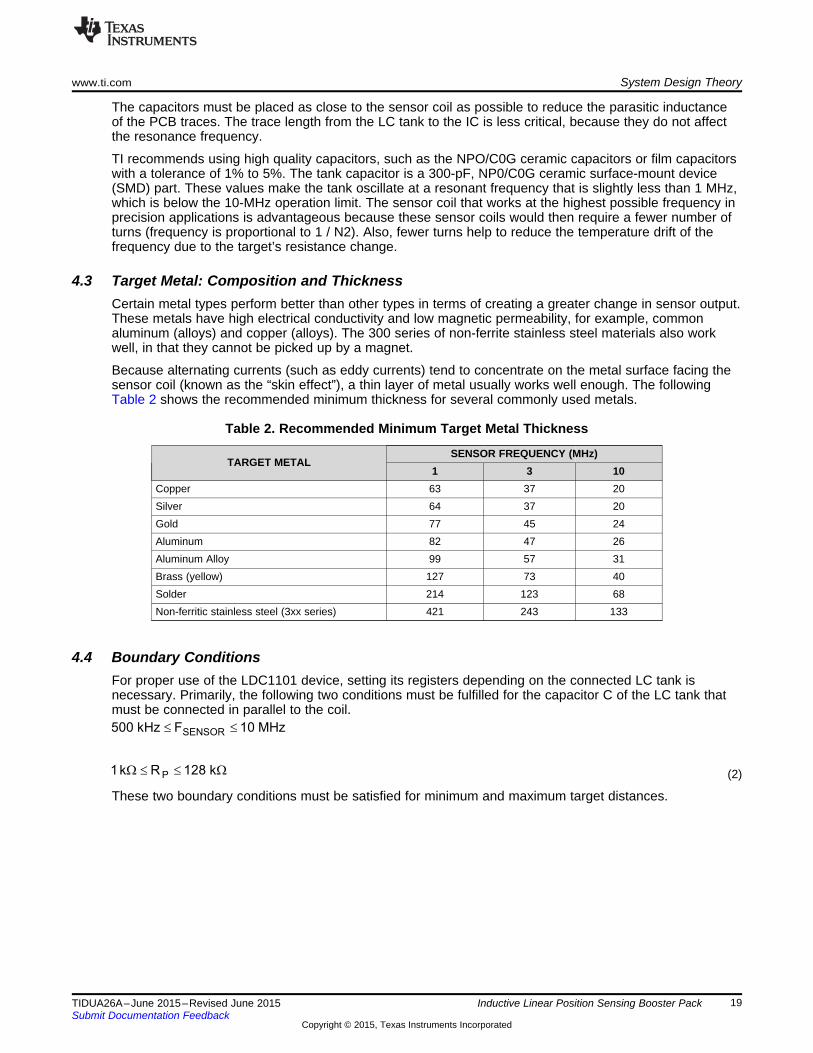
To verify these assumptions, use the FEMM 4.2 (Finite Element Method Magnetics 4.2) magneticsimulation software. Defining the PCB coils in FEMM 4.2 is not a possibility; so, to obtain a basic idea ofthe induced magnetic field, design a cylindrical coil design instead. This time, the coil is axis symmetric tothe x-axis. The coil is divided into eleven sections that are connected in serial, thus carrying the samecurrent. The lengths of the segments add up to 100 mm. The current can be set to any value, becauseonly the basic characteristic of the evolving magnetic field is of importance. To simulate the design of thePCB coils, every segment has a different number of turns, compared to its neighboring segments. Thesimulation result in Figure 16 shows that the magnetic flux density is minimum at dX = 0 mm. Then, themagnetic flux density increases to its maximum at dX = 100 mm, validating the aforementionedassumptions.
Figure 16. Simulated Magnetic Field of Asymmetric Coil
The coil measures 100 mm × 15 mm, has 28 turns per layer on two layers, and a 3.3-mm loop stepping.The AC magnetic field that the coil produces is strongest at its innermost turn and decays towards the left-hand side. Therefore, the peak strength of the AC magnetic field lies right of the geometric center of thecoil. Texas Instruments provides PCB layout scripts that generate stretched coils for linear positionsensing applications. The application report SNOA930 contains further information on LDC sensor design.
17TIDUA26A–June 2015–Revised June 2015 Inductive Linear Position Sensing Booster PackSubmit Documentation Feedback
Copyright © 2015, Texas Instruments Incorporated

System Design Theory www.ti.com
Figure 17, Figure 18, and Figure 19 show different target positions with respect to the sensor coil indifferent views.
Figure 17. Starting Position: dX = 0 mm (Top View)
Figure 18. Final Position: dX = 100 mm (Top View)
Figure 19. Final Position: dX = 100 mm (Side View)
The target length XTARGET impacts resolution and travel range. A longer target improves resolution but limitsthe usable travel range. The target width YTARGET must extend past the coil to ensure maximum metalexposure.
The wide range of oscillation frequency and the driving current of the LDC1101 device provide greatflexibility to the user when selecting the dimensions of the coil that best suits his or her specificmechanical system configuration. However, certain rules must be followed to ensure the proper operationof the device.• LC tank resonant frequency – The recommended sensor frequency range for LDC1101 devices is
500 kHz to 10 MHz.• Inductance of the sensor coil – There is no absolute requirement on the value of the inductance, as
long as the range of the resonant frequency and RP (the parallel loss resistance) are not violated.• RP of the LC tank – The LC tank is “lossy” due to the inductor’s loss and the energy dissipated by the
target metal. This loss can be modeled by a parallel equivalent resistance RP. The more the energyloss in the LC tank, the smaller is the value of RP. The range of RP values that the LDC1101 devicecan be ranges from 1 kΩ to 128 kΩ. Different sensing applications may use different ranges of theresonance impedance RP to measure. The LDC1101 measurement range of RP is controlled by settingthe RP_SET register: RP_MIN and RP_MAX bits. For a given application, RP must never be outsidethe range set by these register values to avoid clipping the measured value. For optimal sensorresolution, the range of RP_MIN to RP_MAX must not be unnecessarily large.
18 Inductive Linear Position Sensing Booster Pack TIDUA26A–June 2015–Revised June 2015Submit Documentation Feedback
Copyright © 2015, Texas Instruments Incorporated
SENSOR
P
500 kHz F 10 MHz
1k R 128 k
£ £
W £ £ W
www.ti.com System Design Theory
The capacitors must be placed as close to the sensor coil as possible to reduce the parasitic inductanceof the PCB traces. The trace length from the LC tank to the IC is less critical, because they do not affectthe resonance frequency.
TI recommends using high quality capacitors, such as the NPO/C0G ceramic capacitors or film capacitorswith a tolerance of 1% to 5%. The tank capacitor is a 300-pF, NP0/C0G ceramic surface-mount device(SMD) part. These values make the tank oscillate at a resonant frequency that is slightly less than 1 MHz,which is below the 10-MHz operation limit. The sensor coil that works at the highest possible frequency inprecision applications is advantageous because these sensor coils would then require a fewer number ofturns (frequency is proportional to 1 / N2). Also, fewer turns help to reduce the temperature drift of thefrequency due to the target’s resistance change.
4.3 Target Metal: Composition and ThicknessCertain metal types perform better than other types in terms of creating a greater change in sensor output.These metals have high electrical conductivity and low magnetic permeability, for example, commonaluminum (alloys) and copper (alloys). The 300 series of non-ferrite stainless steel materials also workwell, in that they cannot be picked up by a magnet.
Because alternating currents (such as eddy currents) tend to concentrate on the metal surface facing thesensor coil (known as the “skin effect”), a thin layer of metal usually works well enough. The followingTable 2 shows the recommended minimum thickness for several commonly used metals.
Table 2. Recommended Minimum Target Metal Thickness
SENSOR FREQUENCY (MHz)TARGET METAL
1 3 10Copper 63 37 20Silver 64 37 20Gold 77 45 24Aluminum 82 47 26Aluminum Alloy 99 57 31Brass (yellow) 127 73 40Solder 214 123 68Non-ferritic stainless steel (3xx series) 421 243 133
4.4 Boundary ConditionsFor proper use of the LDC1101 device, setting its registers depending on the connected LC tank isnecessary. Primarily, the following two conditions must be fulfilled for the capacitor C of the LC tank thatmust be connected in parallel to the coil.
(2)
These two boundary conditions must be satisfied for minimum and maximum target distances.
19TIDUA26A–June 2015–Revised June 2015 Inductive Linear Position Sensing Booster PackSubmit Documentation Feedback
Copyright © 2015, Texas Instruments Incorporated

( )SENSOR _DIV 8 24SENSOR CLKINF F 2 LHR _DATA LHR _ OFFSET 2 2 -= ´ ´ + ´ ´
CLKINSENSOR
F RESP _ TIMESensor Frequency, F
3 L _DATA
´
=
´
CLKIN CLKIN
SENSOR _ at _ 0mm SENSOR _ at _100mm
F FRESP _ TIME
F FCODE
3
æ ö´ -ç ÷
ç ÷è øD =
System Design Theory www.ti.com
4.5 Criterion for Maximizing ResolutionThe number of code words difference between two extreme positions (dX = 0 mm and dX = 100 mm) isdetermined by using Equation 3:
where• FCLKIN is the external time-base clock input into the LDC1101• FSENSOR at 0mm is the resonant frequency of sensor when the target is at position X = 0 mm• FSENSOR at 100mm is the resonant frequency of sensor when the target is at position X = 100 mm• RESP_TIME is the programmed value of the LDC1101 register field RESP_TIME (3)
To achieve the optimum resolution:• Maximize the difference of readings between the “maximum” and “minimum” position of the target over
the sensor. For lateral sensing, the target moves from the least amount of material covering the coil tothe most amount of material covering the coil.
• Use the maximum supported reference frequency ( = 12 MHz).• Use the slowest possible sampling rate (largest response time = 6144).• Improve the resolution further by averaging over multiple samples externally.
4.6 Measuring InductanceThe LDC1101 device measures the sensor’s frequency of oscillation by the use of a frequency counter, asFigure 20 shows. The frequency counter timing is set by an external clock (12 MHz typical) from themicrocontroller and is provided on the CLKIN pin. The sensor resonance frequency is derived from thefrequency counter registers value (see registers 0x23 - 0x24 in RP + L mode and registers 0x38 through0x3A in LHR mode) as follows in Equation 4 and Equation 5.
In RP + L mode:
where• FCLKIN is the frequency input to the CLKIN pin• L_DATA is the contents of registers 0x23 and 0x24• RESP_TIME is the programmed response time in register 0x04 (4)
In LHR mode:
where• FCLKIN is the frequency input to the CLKIN pin• LHR_DATA is the contents of registers 0x38, 0x39, and 0x3A• LHR_OFFSET is the programmed contents of registers 0x32 and 0x33, note that this value is scaled by 256• SENSOR_DIV is the contents of LHR_CONFIG.SENSOR_DIV (register 0x34-bit [1:0]) (5)
20 Inductive Linear Position Sensing Booster Pack TIDUA26A–June 2015–Revised June 2015Submit Documentation Feedback
Copyright © 2015, Texas Instruments Incorporated
( )2
SENSOR
1L
C 2 F
=
´ p
www.ti.com System Design Theory
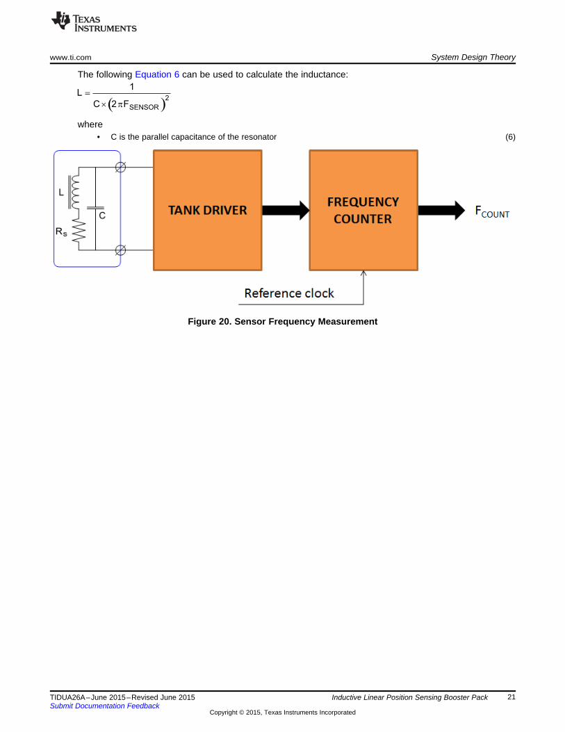
The following Equation 6 can be used to calculate the inductance:
where• C is the parallel capacitance of the resonator (6)
Figure 20. Sensor Frequency Measurement
21TIDUA26A–June 2015–Revised June 2015 Inductive Linear Position Sensing Booster PackSubmit Documentation Feedback
Copyright © 2015, Texas Instruments Incorporated
Metal target
Pattern inductive coil
Linear table
Screw
Motor
TIDA-00460Board
Air gap
Test Setup www.ti.com
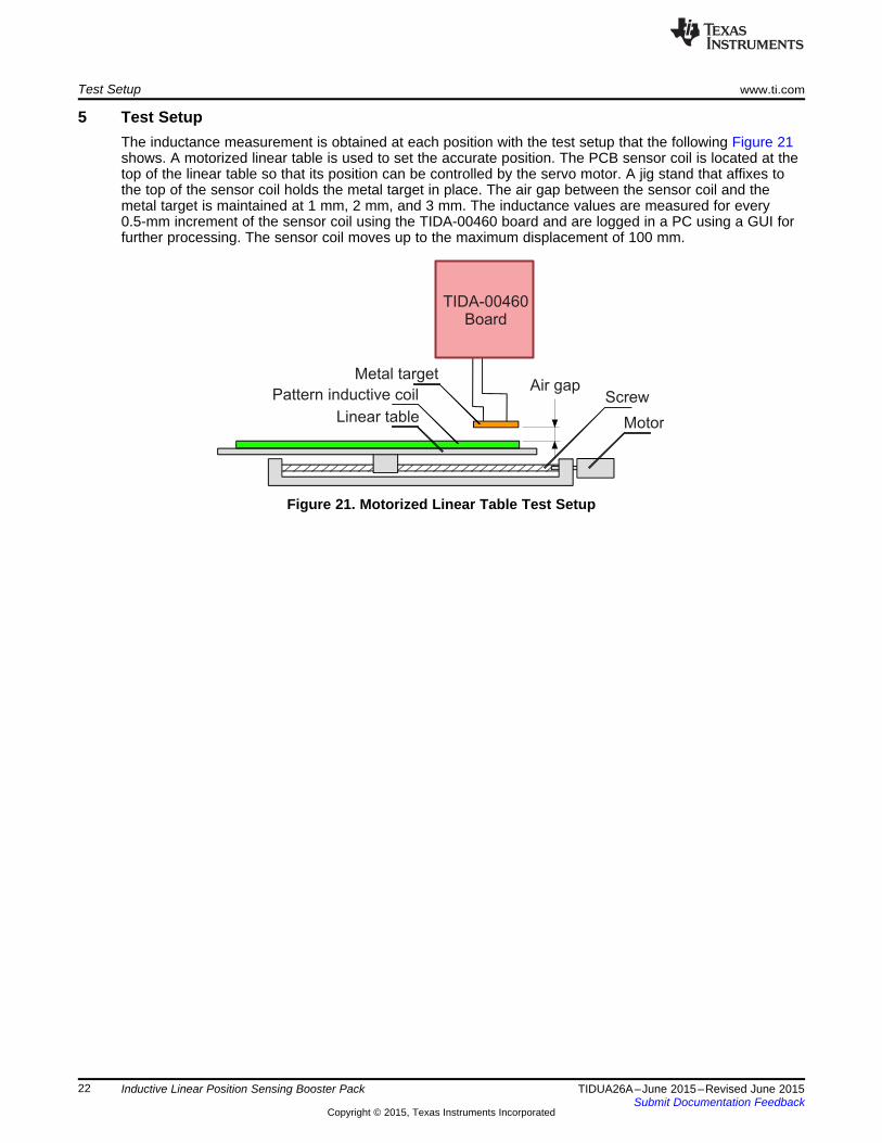
5 Test SetupThe inductance measurement is obtained at each position with the test setup that the following Figure 21shows. A motorized linear table is used to set the accurate position. The PCB sensor coil is located at thetop of the linear table so that its position can be controlled by the servo motor. A jig stand that affixes tothe top of the sensor coil holds the metal target in place. The air gap between the sensor coil and themetal target is maintained at 1 mm, 2 mm, and 3 mm. The inductance values are measured for every0.5-mm increment of the sensor coil using the TIDA-00460 board and are logged in a PC using a GUI forfurther processing. The sensor coil moves up to the maximum displacement of 100 mm.
Figure 21. Motorized Linear Table Test Setup
22 Inductive Linear Position Sensing Booster Pack TIDUA26A–June 2015–Revised June 2015Submit Documentation Feedback
Copyright © 2015, Texas Instruments Incorporated
Optimal Operating RegionReduced Resolution Not Usable
www.ti.com Test Data
6 Test Data
NOTE: The test data in the following sections was measured with the system at room temperature,unless otherwise noted.
All of the measurements in this section were measured with calibrated lab equipment.
Moving a target from dX = 0 mm to dX = 100 mm at an air gap of dZ = 1mm, 2mm, and 3mm in 0.5-mmincrements results in the data output that the following Figure 22 shows. The target is a 14- × 25-mmaluminum target.
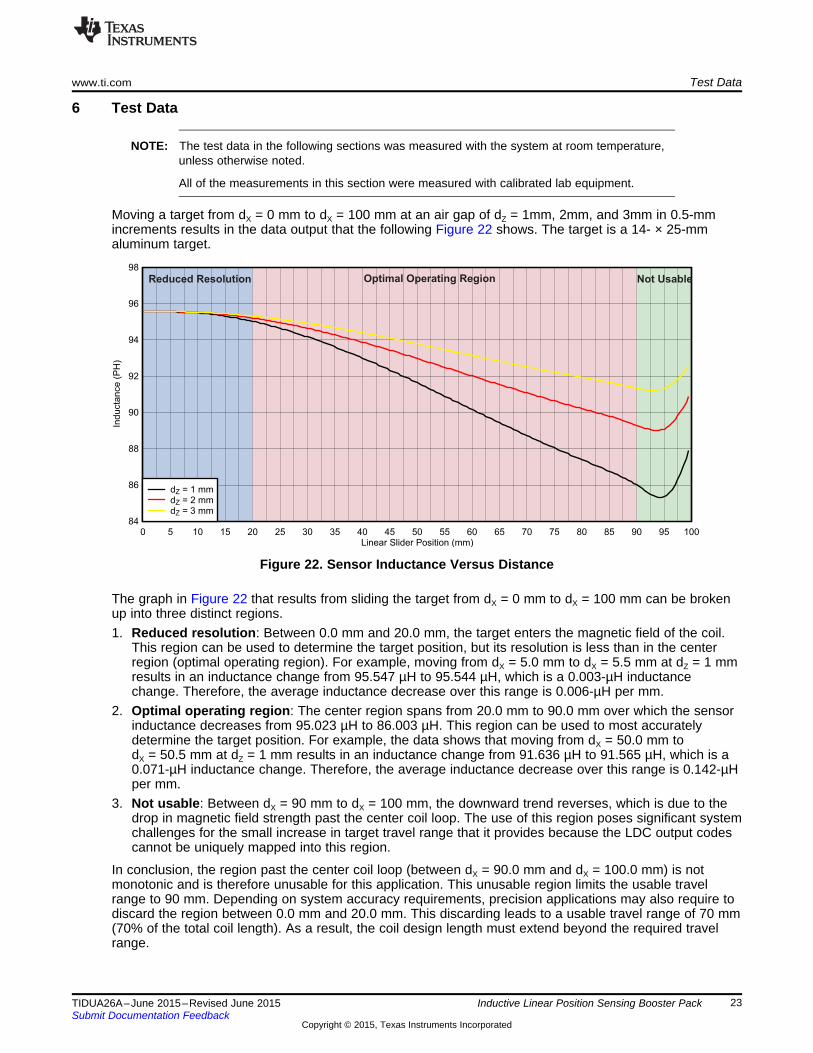
Figure 22. Sensor Inductance Versus Distance
The graph in Figure 22 that results from sliding the target from dX = 0 mm to dX = 100 mm can be brokenup into three distinct regions.1. Reduced resolution: Between 0.0 mm and 20.0 mm, the target enters the magnetic field of the coil.
This region can be used to determine the target position, but its resolution is less than in the centerregion (optimal operating region). For example, moving from dX = 5.0 mm to dX = 5.5 mm at dZ = 1 mmresults in an inductance change from 95.547 µH to 95.544 µH, which is a 0.003-µH inductancechange. Therefore, the average inductance decrease over this range is 0.006-µH per mm.
2. Optimal operating region: The center region spans from 20.0 mm to 90.0 mm over which the sensorinductance decreases from 95.023 µH to 86.003 µH. This region can be used to most accuratelydetermine the target position. For example, the data shows that moving from dX = 50.0 mm todX = 50.5 mm at dZ = 1 mm results in an inductance change from 91.636 µH to 91.565 µH, which is a0.071-µH inductance change. Therefore, the average inductance decrease over this range is 0.142-µHper mm.
3. Not usable: Between dX = 90 mm to dX = 100 mm, the downward trend reverses, which is due to thedrop in magnetic field strength past the center coil loop. The use of this region poses significant systemchallenges for the small increase in target travel range that it provides because the LDC output codescannot be uniquely mapped into this region.
In conclusion, the region past the center coil loop (between dX = 90.0 mm and dX = 100.0 mm) is notmonotonic and is therefore unusable for this application. This unusable region limits the usable travelrange to 90 mm. Depending on system accuracy requirements, precision applications may also require todiscard the region between 0.0 mm and 20.0 mm. This discarding leads to a usable travel range of 70 mm(70% of the total coil length). As a result, the coil design length must extend beyond the required travelrange.
23TIDUA26A–June 2015–Revised June 2015 Inductive Linear Position Sensing Booster PackSubmit Documentation Feedback
Copyright © 2015, Texas Instruments Incorporated
Test Data www.ti.com
The output is mostly linear over 70% of the travel range. Provided that the degree of linearization duringthis range is sufficient to meet the system accuracy requirements, no additional linearization is necessary.However, users often desire a higher degree of linearization to minimize the required coil length andimprove system accuracy. The following two approaches can be used to improve the linearity of themeasurement:1. The output code can be translated to travel distance by calculating the best-fit curve through the output
response. For this approach, system accuracy requirements dictate the minimum polynomial degree,thereby also dictating the required processing power of the microcontroller. The user may incorporatethe coefficients of the polynomial into the microcontroller. When the sensor coil is moved using thelinear table, the microcontroller receives the data from the LDC1101 device and runs the data throughthe polynomial equation using the programmed coefficients, which then generates the distance in mm.
2. The output code can be translated to travel distance by employing a look-up table. This approachrequires little processing power, but requires memory for the look-up table.
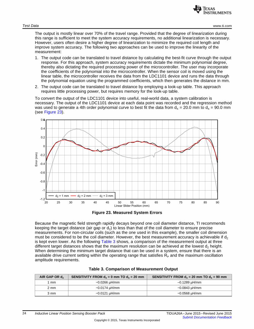
To convert the output of the LDC1101 device into useful, real-world data, a system calibration isnecessary. The output of the LDC1101 device at each data point was recorded and the regression methodwas used to generate a 4th order polynomial curve to best fit the data from dX = 20.0 mm to dX = 90.0 mm(see Figure 23).
Figure 23. Measured System Errors
Because the magnetic field strength rapidly decays beyond one coil diameter distance, TI recommendskeeping the target distance (air gap or dZ) to less than that of the coil diameter to ensure precisemeasurements. For non-circular coils (such as the one used in this example), the smaller coil dimensionmust be considered to be the coil diameter. However, the best measurement accuracy is achievable if dZis kept even lower. As the following Table 3 shows, a comparison of the measurement output at threedifferent target distances shows that the maximum resolution can be achieved at the lowest dZ height.When determining the minimum target distance that can be used in a system, ensure that there is anavailable drive current setting within the operating range that satisfies RP and the maximum oscillationamplitude requirements.
Table 3. Comparison of Measurement Output
AIR GAP OR dZ SENSITIVITY FROM dX = 0 mm TO dX = 20 mm SENSITIVITY FROM dX = 20 mm TO dX = 90 mm1 mm −0.0266 µH/mm –0.1289 µH/mm2 mm −0.0174 µH/mm −0.0843 µH/mm3 mm −0.0121 µH/mm −0.0568 µH/mm
24 Inductive Linear Position Sensing Booster Pack TIDUA26A–June 2015–Revised June 2015Submit Documentation Feedback
Copyright © 2015, Texas Instruments Incorporated

www.ti.com Summary
7 SummaryInductive sensing is an ideal sensing method for linear position sensing due to its contactless nature andhigh reliability. A linear position can be measured either by using a circular coil and a triangular target, orby using a stretched coil and a rectangular target. The space requirements for a coil and target are theprimary deciding factors as to which approach to use for a system. Using a stretched coil and rectangulartarget is suitable for systems in which system space constraints dictate the use of a small target.Texas Instruments provides coil scripts that greatly simplify coil design for this approach.
25TIDUA26A–June 2015–Revised June 2015 Inductive Linear Position Sensing Booster PackSubmit Documentation Feedback
Copyright © 2015, Texas Instruments Incorporated
1
3
56
4
2
7
910
8
12 11
14 13
16 15
18 17
20 19
J4
SSW-110-23-F-D
1
3
56
4
2
7
910
8
12 11
14 13
16 15
18 17
20 19
J2
SSW-110-23-F-D
GND
MSP_DP
MSP_DM
GND
GND
2.2µFC3
GND
VCC1
NC2
IO13
GND4
IO25
U2
TPD2E001DRLR
L1
VLS201610ET-100M
VBUS
GND
VBUS1
D-2
D+3
ID4
GND5
67
8
11
10
913
12
J3ZX62R-B-5P
DMroute
UGND
0.1µFC7
1MR3
5.6V
21
D1
GND
SH-J1 VBUS LDO_IN
GND GND
0.1µFC2
MSP_DPMSP_DM
MSP_PUR
P6.0/CB0/A01
P6.1/CB1/A12
P6.2/CB2/A23
P6.3/CB3/A34
P6.4/CB4/A45
P6.5/CB5/A56
P6.6/CB6/A67
P6.7/CB7/A78
P5.0/A8/VREF+/VEREF+9
P5.1/A9/VREF-/VEREF-10
AVCC111
P5.4/XIN12
P5.5/XOUT13
AVSS114
DVCC115
DVSS116
VCORE17
P1.0/TA0CLK/ACLK18
P1.1/TA0.019
P1.2/TA0.120
P1.3/TA0.221
P1.4/TA0.322
P1.5/TA0.423
P1.6/TA1CLK/CBOUT24
P1.7/TA1.025
P2.0/TA1.126
P2.1/TA1.227
P2.2/TA2CLK/SMCLK28
P2.3/TA2.029
P2.4/TA2.130
P2.5/TA2.231
P2.6/RTCCLK/DMAE032
P2.7/UCB0STE/UCA0CLK33
P3.0/UCB0SIMO/UCB0SDA34
P3.1/UCB0SOMI/UCB0SCL35
P3.2/UCB0CLK/UCA0STE36
P3.3/UCA0TXD/UCA0SIMO37
P3.4/UCA0RXD/UCA0SOMI38
DVSS239
DVCC240
P4.0/PM_UCB1STE/PM_UCA1CLK41
P4.1/PM_UCB1SIMO/PM_UCB1SDA42
P4.2/PM_UCB1SOMI/PM_UCB1SCL43
P4.3/PM_UCB1CLK/PM_UCA1STE44
P4.4/PM_UCA1TXD/PM_UCA1SIMO45
P4.5/PM_UCA1RXD/PM_UCA1SOMI46
P4.6/PM_NONE47
P4.7/PM_NONE48
VSSU49
PU.0/DP50
PUR51
PU.1/DM52
VBUS53
VUSB54
V1855
AVSS256
P5.2/XT2IN57
P5.3/XT2OUT58
TEST/SBWTCK59
PJ.0/TDO60
PJ.1/TDI/TCLK61
PJ.2/TMS62
PJ.3/TCK63
RST/NMI/SBWTDIO64
QFN PAD65
U4
MSP430F5528IRGC
GNDGND
1.0kR8
1.0k
R7
TP9
GND
CLK_MSP
MCU_CLKIN
MCU_SCLK
SDO
MCU_CSB
GLEDRLED
GLEDA RLEDA
MCLK
MSPV18MSPVCore
220nFC18
MSP_XT2
GPIO2
GND
1
34
2GG
24MHz
Y1ABM8-24.000MHZ-B2-T
MCU_SDI
18pFC13
18pFC14
GND GND GND
10µFC23
0.1µFC25
GND
GND
GND
2200pFC15
SBWTDIOSBWTCK
33kR9
+3.3V_LDO
TP10
If two bypass capacitors are used, populatesmaller value on C1 footprint
+5V_LP
GND
GND
18pFC16
GND
18pFC17
GND
330pFC_TANK
18pFC21
18pFC22
INA
INB
COILA
COILB
MSP_PUR
DProute
0.1µFC26
0.1µFC27
0.47µFC19
GND
GLED RLED
GND
CLKIN2
SCLK3
SDI4
CSB5
GND8
INB6
INA7
SDO/INTB1
VDD9
CLDO10
PAD11
U5
LDC1101DRC
GND
0.015µFC12
GND
TP3
MCU_CLKIN
MCU_SCLK
0.1µFC11
1µFC10
INA
INB
SDO
MCU_SDI
MCU_CSB
MOSI_BPMISO_BPSCLK_BP
CS_BP
1
2
3
J1
PEC03SAAN
Super Red
21
D3Green
21
D2
0
R10
0
R11
1
2
J6
PPTC021LGBN-RC
TP4
TP8
+3.3V_LP
SH-J71
2
3
J7
PEC03SAAN
+3.3V
220nFC20
VBUS
4.7µFC6
IN1
OUT5
2
EN3
NC4
GND
U1LP5951MG-3.3/NOPB
+5V_LP
+3.3V_LDO +3.3V_LP
+3.3V
1
2
J8
TSW-102-07-T-S
+3.3V
SH-J8
+3.3V
+3.3V
1 2
3 4
5 6
7 8
9 10
11 12
13 14
J5
SBH11-PBPC-D07-ST-BKGND
Spy-bi-wire Interface & ESD Protection
GND
123
J9PEC03SAAN
+3.3V
SH-J9
VCC_TOOLVCC_TARGET
SBWTDIO
SBWTCK
UART_TXDUART_RXD
UART_TXD
SCLK_BP
MOSI_BPMISO_BP
CS_BP
TIDA-00460 Powered By
+3.3V from Launch Pad
+5V from Launch Pad
VBUS
MSP430 FET Tool
J1 J7 J9
Don't Care Short 2-3
Short 2-3 Short 1-2
All Open Short 2-3
Short 1-2 Short 1-2
Don't Care
Short 1-2
Short 1-2
Short 1-2
GND GND
D4
SBR0220T5-7-F
27R2
27R4
1.40kR1
10pFC5
10pFC8
GND GND
21S2
100R15
2.2µFC1
VUSB
SH-J10
+3.3V
J10
VBUS & MSP430's Built-in LDO
1
2
J10
TSW-102-07-T-S
VUSB
Open
Open
Open
Open
Short 1-2Don't Care All Open Short 1-2
33R5
11
22
U6
TPD1E10B06DPYR
11
22
U3
TPD1E10B06DPYR
4.99R14
0R12
0R13
UART_RXD
GPIO1
GPIO3
GPIO2GPIO1
GPIO3
Design Files www.ti.com
8 Design Files
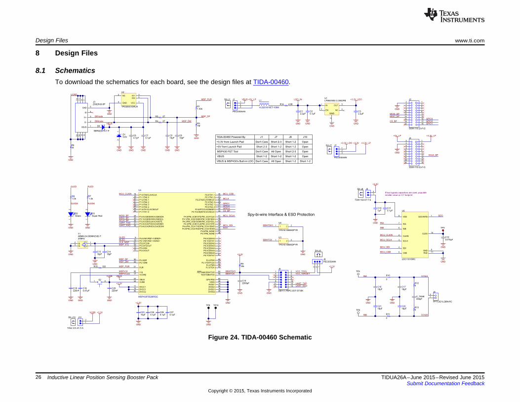
8.1 SchematicsTo download the schematics for each board, see the design files at TIDA-00460.
Figure 24. TIDA-00460 Schematic
26 Inductive Linear Position Sensing Booster Pack TIDUA26A–June 2015–Revised June 2015Submit Documentation Feedback
Copyright © 2015, Texas Instruments Incorporated
www.ti.com Design Files
8.2 Bill of MaterialsTo download the bill of materials (BOM), see the design files at TIDA-00460.
8.3 Layout PrintsTo download the layout prints for each board, see the design files at TIDA-00460.
8.4 Altium ProjectTo download the Altium project files, see the design files at TIDA-00460.
8.5 Gerber FilesTo download the Gerber files, see the design files at TIDA-00460.
8.6 Assembly DrawingsTo download the assembly drawings for each board, see the design files at TIDA-00460.
9 References
1. Texas Instruments, LDC1101 1.8 V High-Resolution, High-Speed Inductance-to-Digital Converter,LDC1101 Datasheet (SNOSD01)
2. Texas Instruments, LDC1101EVM User Guide, LDC1101EVM User’s Guide (SNOU137)3. Texas Instruments, LDC1612/LDC1614 Linear Position Sensing,
LDC1612/LDC1614 Application Report (SNOA931)4. Texas Instruments, Configuring Inductive-to-Digital-Converters for Parallel Resistance (RP) Variation in
L-C Tank Sensors, LDC1xxx Family Application Report (SNAA221)5. Texas Instruments, TI E2E Community, TI E2E™ Online Community Forum (http://e2e.ti.com/)
27TIDUA26A–June 2015–Revised June 2015 Inductive Linear Position Sensing Booster PackSubmit Documentation Feedback
Copyright © 2015, Texas Instruments Incorporated

IMPORTANT NOTICE FOR TI REFERENCE DESIGNS
Texas Instruments Incorporated ("TI") reference designs are solely intended to assist designers (“Buyers”) who are developing systems thatincorporate TI semiconductor products (also referred to herein as “components”). Buyer understands and agrees that Buyer remainsresponsible for using its independent analysis, evaluation and judgment in designing Buyer’s systems and products.TI reference designs have been created using standard laboratory conditions and engineering practices. TI has not conducted anytesting other than that specifically described in the published documentation for a particular reference design. TI may makecorrections, enhancements, improvements and other changes to its reference designs.Buyers are authorized to use TI reference designs with the TI component(s) identified in each particular reference design and to modify thereference design in the development of their end products. HOWEVER, NO OTHER LICENSE, EXPRESS OR IMPLIED, BY ESTOPPELOR OTHERWISE TO ANY OTHER TI INTELLECTUAL PROPERTY RIGHT, AND NO LICENSE TO ANY THIRD PARTY TECHNOLOGYOR INTELLECTUAL PROPERTY RIGHT, IS GRANTED HEREIN, including but not limited to any patent right, copyright, mask work right,or other intellectual property right relating to any combination, machine, or process in which TI components or services are used.Information published by TI regarding third-party products or services does not constitute a license to use such products or services, or awarranty or endorsement thereof. Use of such information may require a license from a third party under the patents or other intellectualproperty of the third party, or a license from TI under the patents or other intellectual property of TI.TI REFERENCE DESIGNS ARE PROVIDED "AS IS". TI MAKES NO WARRANTIES OR REPRESENTATIONS WITH REGARD TO THEREFERENCE DESIGNS OR USE OF THE REFERENCE DESIGNS, EXPRESS, IMPLIED OR STATUTORY, INCLUDING ACCURACY ORCOMPLETENESS. TI DISCLAIMS ANY WARRANTY OF TITLE AND ANY IMPLIED WARRANTIES OF MERCHANTABILITY, FITNESSFOR A PARTICULAR PURPOSE, QUIET ENJOYMENT, QUIET POSSESSION, AND NON-INFRINGEMENT OF ANY THIRD PARTYINTELLECTUAL PROPERTY RIGHTS WITH REGARD TO TI REFERENCE DESIGNS OR USE THEREOF. TI SHALL NOT BE LIABLEFOR AND SHALL NOT DEFEND OR INDEMNIFY BUYERS AGAINST ANY THIRD PARTY INFRINGEMENT CLAIM THAT RELATES TOOR IS BASED ON A COMBINATION OF COMPONENTS PROVIDED IN A TI REFERENCE DESIGN. IN NO EVENT SHALL TI BELIABLE FOR ANY ACTUAL, SPECIAL, INCIDENTAL, CONSEQUENTIAL OR INDIRECT DAMAGES, HOWEVER CAUSED, ON ANYTHEORY OF LIABILITY AND WHETHER OR NOT TI HAS BEEN ADVISED OF THE POSSIBILITY OF SUCH DAMAGES, ARISING INANY WAY OUT OF TI REFERENCE DESIGNS OR BUYER’S USE OF TI REFERENCE DESIGNS.TI reserves the right to make corrections, enhancements, improvements and other changes to its semiconductor products and services perJESD46, latest issue, and to discontinue any product or service per JESD48, latest issue. Buyers should obtain the latest relevantinformation before placing orders and should verify that such information is current and complete. All semiconductor products are soldsubject to TI’s terms and conditions of sale supplied at the time of order acknowledgment.TI warrants performance of its components to the specifications applicable at the time of sale, in accordance with the warranty in TI’s termsand conditions of sale of semiconductor products. Testing and other quality control techniques for TI components are used to the extent TIdeems necessary to support this warranty. Except where mandated by applicable law, testing of all parameters of each component is notnecessarily performed.TI assumes no liability for applications assistance or the design of Buyers’ products. Buyers are responsible for their products andapplications using TI components. To minimize the risks associated with Buyers’ products and applications, Buyers should provideadequate design and operating safeguards.Reproduction of significant portions of TI information in TI data books, data sheets or reference designs is permissible only if reproduction iswithout alteration and is accompanied by all associated warranties, conditions, limitations, and notices. TI is not responsible or liable forsuch altered documentation. Information of third parties may be subject to additional restrictions.Buyer acknowledges and agrees that it is solely responsible for compliance with all legal, regulatory and safety-related requirementsconcerning its products, and any use of TI components in its applications, notwithstanding any applications-related information or supportthat may be provided by TI. Buyer represents and agrees that it has all the necessary expertise to create and implement safeguards thatanticipate dangerous failures, monitor failures and their consequences, lessen the likelihood of dangerous failures and take appropriateremedial actions. Buyer will fully indemnify TI and its representatives against any damages arising out of the use of any TI components inBuyer’s safety-critical applications.In some cases, TI components may be promoted specifically to facilitate safety-related applications. With such components, TI’s goal is tohelp enable customers to design and create their own end-product solutions that meet applicable functional safety standards andrequirements. Nonetheless, such components are subject to these terms.No TI components are authorized for use in FDA Class III (or similar life-critical medical equipment) unless authorized officers of the partieshave executed an agreement specifically governing such use.Only those TI components that TI has specifically designated as military grade or “enhanced plastic” are designed and intended for use inmilitary/aerospace applications or environments. Buyer acknowledges and agrees that any military or aerospace use of TI components thathave not been so designated is solely at Buyer's risk, and Buyer is solely responsible for compliance with all legal and regulatoryrequirements in connection with such use.TI has specifically designated certain components as meeting ISO/TS16949 requirements, mainly for automotive use. In any case of use ofnon-designated products, TI will not be responsible for any failure to meet ISO/TS16949.IMPORTANT NOTICE
Mailing Address: Texas Instruments, Post Office Box 655303, Dallas, Texas 75265Copyright © 2015, Texas Instruments Incorporated


![ProSense Basic M18 Inductive Proximity SensorsProsense Basic M18 Inductive Proximity Sensor Specifications Mounting Type Flush Non-flush Nominal Sensing Distance 5mm [0.20 in] 8mm](https://static.fdocuments.in/doc/165x107/60bb37da50106b1d446ec719/prosense-basic-m18-inductive-proximity-sensors-prosense-basic-m18-inductive-proximity.jpg)


![THE JOURNAL OF APPLIED SENSING TECHNOLOGY The Next ... Duncan/automotive... · • Capacitive [4] • Inductive LVDT/RVDT [5,6,7] • Planar coil inductive [8] • Hall effect [9,10]](https://static.fdocuments.in/doc/165x107/5f4f0808836cd62ff016560e/the-journal-of-applied-sensing-technology-the-next-duncanautomotive-a.jpg)


