
Indoor photovoltaics with Perovskite solar cells and ...
64
1 Indoor photovoltaics with Perovskite solar cells and nanostructured surfaces Nathalie Carrier
Transcript of Indoor photovoltaics with Perovskite solar cells and ...
1
Indoor photovoltaics with Perovskite solar
cells and nanostructured surfaces
Nathalie Carrier

2
TRITA-FYS 2016:01ISSN 0280-316XISRN KTH/FYS/–16:01—SE

3
Abstract
This work is a contribution to the development of a high efficiencyphotovoltaic cell adapted to indoor environment.
Indoor light has been defined and a power of approximately 0.8 mWhas been calculated to be available for harvesting, allowing the supply oflow power sensors.
A CH3NH3PbI3 Perovskite simulation has shown that this Perovskitehas a quantum efficiency close to 1 over visible range using a hole trans-port material. It stands for good candidate to replace conventional a-Sias indoor light harvester.
Finally nanostructured films have been investigated in order to im-prove diffuse light harvesting. The deposition of a Polystyrene beadsmonolayer on top of the cell front surface has been performed. Experi-ments and simulations have shown resonances. More studies are neededto conclude on the enhancement this nanostructuration can provide.
Acknowledgement
Firstly I would like to thank Jean-Claude Bourgoint, director atGreen ITN at Orange Labs and Stephane Le Masson, head of Researchfor Energy and Environment Department at Orange Labs for welcomingme as a trainee.
My thanks also go to Dr. Thomas Rivera, Research project managerat Orange Labs Networks, who supervised and mentored my work, forhis attention, and for all the time he awarded to me.
I would like to thank Dr. Christian Tanguy, Researcher at OrangeLabs Networks, for sharing with me a piece of his knowledge about re-fractive indices analytical models.
I would like to thank every person I have worked with within thesefew months, among them: Pr. Serge Ravaine, Pr. Thierry Toupance,Christian Bourliataud, Emeline Beaudri, Jose Parra-Dıaz.
Finally, I would like to thank Pr David Haviland, my KTH supervi-sor, who helped me realizing that work and who gave me all his attention.
Contents
Contents 4
List of Figures 6
List of Tables 7
List of Abbreviations 8
1 Introduction 91.1 Background . . . . . . . . . . . . . . . . . . . . . . . . . . . . . 91.2 Objectives . . . . . . . . . . . . . . . . . . . . . . . . . . . . . . 111.3 Methodology . . . . . . . . . . . . . . . . . . . . . . . . . . . . 11
2 Towards optimal indoor PV 132.1 Ideal band gap calculation . . . . . . . . . . . . . . . . . . . . . 132.2 Validation on solar spectrum . . . . . . . . . . . . . . . . . . . 152.3 Application to LED spectrum . . . . . . . . . . . . . . . . . . . 17
3 Design of a planar Perovskites-based photovoltaics device 223.1 Introduction to Perovskites . . . . . . . . . . . . . . . . . . . . 223.2 Photovoltaic cell design . . . . . . . . . . . . . . . . . . . . . . 263.3 Optical characterization . . . . . . . . . . . . . . . . . . . . . . 26
4 Planar cell quantum efficiency 294.1 Heterojunction QE calculation . . . . . . . . . . . . . . . . . . 294.2 N-P heterojunction structure . . . . . . . . . . . . . . . . . . . 344.3 N-I-P heterojunction structure . . . . . . . . . . . . . . . . . . 37
5 Photonic crystal towards higer performances 415.1 Introduction to photonic crystals . . . . . . . . . . . . . . . . . 415.2 Photonic crystal choice . . . . . . . . . . . . . . . . . . . . . . . 42
4

CONTENTS 5
5.3 Apparatus experimental . . . . . . . . . . . . . . . . . . . . . . 435.4 Finite Difference Time Domain method . . . . . . . . . . . . . 455.5 Experimental results and comparison with simulations . . . . . 45
6 Conclusion and perspectives 50
Bibliography 51
A Ideal bad gap calculation code 55
B Abeles calculation 57
C Material indices modelisation 62
List of Figures
1.1 NREL Best Research-Cell Efficiencies. . . . . . . . . . . . . . . . . 12
2.1 AM1.5G solar spectral irradiance. . . . . . . . . . . . . . . . . . . 16
2.2 Solar maximum efficiency curve. . . . . . . . . . . . . . . . . . . . 16
2.3 Normalized solar spectrum (black) and comparison between maxi-mum efficiency curve (red) and the integral for E > Eg of normal-ized solar irradiance (blue). . . . . . . . . . . . . . . . . . . . . . . 17
2.4 LED light cone representation. . . . . . . . . . . . . . . . . . . . . 18
2.5 Solar and LED spectra in arbitrary units. . . . . . . . . . . . . . . 19
2.6 LED maximum efficiency curve. . . . . . . . . . . . . . . . . . . . . 19
2.7 Normalized LED spectrum (black) and comparison between maxi-mum efficiency curve (red) and the integral for E > Eg of normal-ized LED irradiance (blue). . . . . . . . . . . . . . . . . . . . . . . 20
3.1 Perovskite cell structures: planar structure without scaffold andmesoporous structure with scaffold. . . . . . . . . . . . . . . . . . . 23
3.2 Ideal crystal structure of perovskite materials [16]. . . . . . . . . . 24
3.3 Absorption spectra of Formamidinium Lead Iodide with mixedhalogen [17]. . . . . . . . . . . . . . . . . . . . . . . . . . . . . . . 25
3.4 Planar structure design. . . . . . . . . . . . . . . . . . . . . . . . . 26
3.5 Absorption coefficient (α) for ITO, TiO2 and PVK in visible range. 27
3.6 Planar cell absorption in P polarization. . . . . . . . . . . . . . . . 28
3.7 Planar cell absorption in S polarization. . . . . . . . . . . . . . . . 28
4.1 Structure of the p-n heterojunction. . . . . . . . . . . . . . . . . . 30
4.2 Band structure of a TiO2/CH3NH3PbI3 heterojunction [26]. . . . . 34
4.3 Structure of the p-n heterojunction: TiO2/PVK. . . . . . . . . . . 34
4.4 Total spectral response of TiO2/CH3NH3PbI3 n-p heterojunction. 35
4.5 Screen shot of Mathematica program for QE calculation of n-pstructure: TiO2/CH3NH3PbI3. . . . . . . . . . . . . . . . . . . . . 36
6
4.6 TiO2/CH3NH3PbI3/SpiroOmeTAD band structure [27]. . . . . . . 374.7 TiO2/CH3NH3PbI3/SpiroOmeTAD n-i-p heterojunction. . . . . . 384.8 QE of both PVK-based cells compared with a-Si:H external QE [29]. 394.9 Screen shot of Mathematica program for QE calculation of n-i-p
structure: TiO2/CH3NH3PbI3/SpiroOmeTAD. . . . . . . . . . . . 40
5.1 Illustration of one, two and three dimensional photonic crystal [29]. 415.2 Nanospheres deposited on top of Si solar cell [30]. . . . . . . . . . . 425.3 Nanostructured sample illustration. . . . . . . . . . . . . . . . . . . 435.4 PS beads mono-layer of 450 nm diameter. . . . . . . . . . . . . . . 435.5 Change in color of the nanostructured sample with angle. . . . . . 445.6 Set-up experiment. . . . . . . . . . . . . . . . . . . . . . . . . . . . 445.7 Definition of the domain of calculation. . . . . . . . . . . . . . . . 465.8 Transmission of nanostructured sample for P polarization. . . . . . 475.9 Transmission of nanostructured sample for S polarization. . . . . . 475.10 Comparison between FDTD simulation and experiment. . . . . . . 485.11 Planar and nanostructured front film of the cell. . . . . . . . . . . 485.12 Transmission spectra (P polarization) of planar vs nanostructured
sample with angle. . . . . . . . . . . . . . . . . . . . . . . . . . . . 49
C.1 Sellmeier model for Glass and Polystyrene. . . . . . . . . . . . . . 63C.2 ITO indices fit. . . . . . . . . . . . . . . . . . . . . . . . . . . . . . 64
List of Tables
4.1 Indexes definition for QE calculation. . . . . . . . . . . . . . . . . 304.2 Notations. . . . . . . . . . . . . . . . . . . . . . . . . . . . . . . . . 314.3 Parameters for n-p junction. . . . . . . . . . . . . . . . . . . . . . . 354.4 Parameters for the n-i-p junction. . . . . . . . . . . . . . . . . . . . 38
7

List of Abbreviations
AR Anti-reflectionBG Band gapEQE External Quantum efficiencyFDTD Finite difference time domainIoT Internet of thingsIPV Indoor photovoltaicsPC Photonic crystalPCE Power conversion efficiencyPS PolystyrenePV PhotovoltaicsPVK PerovskitesQE Quantum efficiencyQFL Quasi-Fermi level
8
Chapter 1
Introduction
1.1 Background
The Internet of Things (IoT) is a physical objects network. These objectscollect and exchange data thanks to embedded network connectivity. Expertsestimate that IoT will connect no less than 50 billion objects by 2020.
Expected-life time for such devices must match with standard life-timesof radio systems, about 10-15 years. Supplying power to these objects mustbe solved, as batteries will not last this long. Maintenance costs are an issueand batteries replacement is expensive for Telecom. Orange is working onself-fed energy solutions. Several physical effects (thermoelectrocity effect,piezoelectric effect...) could be implemented but the most suitable one seemsto be photovoltaic (PV) powersupply. For home IoT networks (temperaturesensors, motion sensors, ect.), a specific PV solution is required.
Unlike solar illumination, indoor light is limited in spectral range, spanningonly the visible, and often emanating from diffuse and disturbed sources oflow intensity. LEDs are expected to dominate indoor lighting in the followingyears. Consequently LED spectrum is considered. PV technology needs to beadapted to such environment.
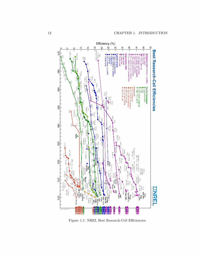
Since 1976, Amorphous Silicon (a-Si) has been dominating the indoor pho-tovoltaic (IPV) market as it is cheap to manufacture, has 10 years life-time andit reacts well under weak intensity. a-Si has already been commercialized tosupply small devices like calculators. However its power conversion efficiencyin the laboratory has not exceed 13.4% (See Figure 1.1) and commercial cellshave not exceeded 6 to 8% [1]. Moreover their efficiency decreases by 10 to20% in the 6 first months of use due to the Staebler–Wronski effect [2]. This
9
10 CHAPTER 1. INTRODUCTION
study focus on Perovskite based photo voltaic materials, a new material toreplace a-Si.
Perovskite as the new a-Si
Aside from the predominant development of silicon-based solar cells, organicsolar cells have been developing and particularly Pervoskite-based solar cellshave recently stood out with the most rapid growth in efficiency in the PVhistory (See Figure 1.1).
These organic Perovskite (PVK) solar cells are based on materials fromthe perovskite family. In only one year of study a 15% Power ConversionEfficiency has been certified [3] and a proven efficiency of 20% has recentlybeen confirmed by NREL (See Figure 1.1).
PVK have a strong absorption below their band gap1 (α ≈ 105 cm−1[4]at 550 nm, which is ten times crystalline Silicon (c-Si) absorption), and thelatter is adapted to visible (cutoff wavelength at around 800 nm) so they aresuited for indoor and thin film applications. Moreover, PVK are easy, fast andcheap to manufacture (five time cheaper than Silicon [5]). They stand out aspromising candidates for large-scale production and widespread applications.
Nanostructuring for higher efficiency
A photonic crystal (PC) is a periodic structure with a pitch of order onehundred nanometers that affects the propagation of photons, as an ionic latticeaffects electrons propagation in solids. PCs have emerged since 1987 withYablonovich’s first article [6].
PCs can contribute to enhance PV efficiency. For example, nanostructuredsurfaces have already been placed on a-Si solar cells [7] from a collaborationbeetween the Nanotechnologies Institute of Lyon (INL) and Orange. A com-plementary study has shown that LED spectra are absorbed up to 90% thanksto the nanostructured surface [8]. Nanostructured PVK based solar cells arepromising too.
The challenge with PC is that 1: they need to be made precisely enoughto prevent scattering losses and 2: a robust and cheap manufacturing processneeds to be designed. Orange is working with the CRPP french laboratory2
which knows how to create photonic devices easily, at low cost, in short timeand with a reproducible bottom-up approach. This so-called ”Inverse Opal”technique could be transferred to large scale mass production. Inverse Opal
1below in terms of wavelenght or above in terms of energy.2CRPP: Centre de Recherche Paul Pascal, Bordeaux I
1.2. OBJECTIVES 11
process consists of the deposition of Polystyrene or Silica beads followed byan infiltration step and with subsequent removal of the beads.
This study focuses on a nanostructured device able to increase the accep-tance angle of a solar cell, or in other words, adapted to diffuse illumination(in contrast to solar beams). Another way nanostructuring could enhance PVperformance would be by increasing the optical path inside the active material.
1.2 Objectives
On the one hand PVK is a good absorbent and well adapted to weak il-lumination in the visible range. On the other hand, nanostructuration canenhance photovoltaics performance by increasing the cell’s acceptance cone.
The goals of this study is to give a first understanding of Perovskite photo-voltaics matched to indoor environment. A first planar structure is studied andlater on the objective is to see how simple nanostructuring improves angularcollection. The simple nanostructuring studied is a monolayer of Polystyrene(PS) beads deposited on top of a planar cell.
1.3 Methodology
The LED spectrum is first studied. Similar to the 33% limit for solar ir-radiance, a calculation of the best gap energy is performed. A planar cellis designed and studied by a classic analytical method: the Matrix TransferMethod. Its Quantum Efficiency (QE) is simulated and compared with a-SiQE.
Finally the contribution of nanostructuring is studied. First of all, thenumerical Finite Difference Time Domain method is introduced. A monolayerof PS beads deposited on a glass substrate is experimentally characterized andnumerically simulated with FDTD method. A discussion about the possibilityof enhancement is proposed.
12 CHAPTER 1. INTRODUCTION
Figure 1.1: NREL Best Research-Cell Efficiencies.
Chapter 2
Towards optimal indoor PV
In this part a study of indoor environment is proposed. More precisely,the maximum conversion efficiency expected from a LED spectrum is derived,similar to the famous Shockley-Queisser limit on the maximum possible effi-ciency of solar cells which states that p-n junctions solar cells are limited toaround 30 % efficiency [9]. Later on this limit has been revised to around 33%at 1.4 eV.
In this section the calculation of the optimized gap is adapted to the LEDspectrum. The Mathematica code is inspired by code from Steve Byrnes [10].
2.1 Ideal band gap calculation
From the irradiance spectrum (Ir) between λmin and λmax (expressed inW.m−2.nm−1), the number of photons per unit time, per unit energy-range,per unit area can be expressed as:
Nphotons =λ
E2× Ir
[1
s m2 J
](1)
The total number of photons with energy above the band gap is obtainedfrom the integral of Nphotons from Eg to Emax.
NE>Eg =
∫ Emax
Eg
Nphotons(E) dE (2)
Some of these photons do not lead to the creation of an electron-hole pairdue to recombination processes. For a direct band gap junction recombina-tion happens predominantly through radiative recombination. Like Shockley
13
14 CHAPTER 2. TOWARDS OPTIMAL INDOOR PV
and Queisser’s first calculations [9], only radiative recombinations are consid-ered, proportional to the product of the electron and hole density, n and prespectively;
R ∝ np (3)
Electron density in a junction is related to electrons Quasi-Fermi level (QFL),and hole density is related to holes QFL. In order to derive the radiativerecombination rate (Rrad), the case when electrons and holes QFLs are equalis first detailed and then extended to the case when QFLs split.
No QFL splitting
This configuration is equivalent to a solar cell at zero bias in the dark,under thermal equilibrium. The semiconductor is assumed to behave like aperfect blackbody above the band gap (BG) and to be transparent below, theradiative recombination rate is expressed:
Rrad0(Eg) =2π
c2h3
∫ Emax
Eg
E2
exp(
EkBTcell
)− 1
dE (4)
QFL splitting
When the electron QFL moves by E1 towards the conduction band, thenew electron concentration is expressed as:
n′ = n× exp
(−E1
kBTcell
)(5)
Similarly when the holes QFL moves by E2 towards the valence band:
p′ = p× exp
(E2
kBTcell
)(6)
To sum up np ∝ exp(
EkBTcell
)with E the total QFL splitting. In the best
possible case, the QFL splitting is equal to the external voltage (it can belarger) leading to:
Rrad(Eg, V ) =Rrad0(Eg)× exp
(eV
kBTcell
)(7)
=2π
c2h3exp
(eV
kBTcell
)∫ Emax
Eg
E2
exp(
EkBTcell
)− 1
dE
2.2. VALIDATION ON SOLAR SPECTRUM 15
The above expression is simplified according to Wurfel and Ruppel’s cal-culation [11]. They conclude that it would be more accurate to use:
2π
c2h3
∫ Emax
Eg
E2
exp(E−eVkBTcell
)− 1
dE (8)
but the difference is negligible for gaps above 200 meV.The current density can be expressed as the electric charge times the num-
ber of photons above the band gap which to not recombine:
J(V,Eg) = e× (NE>Eg(Eg)−Rrad(Eg, V )) (9)
The short circuit current is simply expressed as the current density at zerovoltage:
Jsc(Eg) = J(0, Eg) (10)
The open-circuit voltage is obtained solving J(V,Eg) = 0:
Voc =kBTcelle
× logNE>Eg(Eg)
Rrad0(Eg)(11)
The maximum power point on the I-V curve defined by Vmp and Jmp canbe find solving:
d
dE(V × J(V,Eg)) = 0 (12)
Finally the maximum efficiency as a function of band gap is derived:
ηmax(Eg) =Pmaxout
Pin=VmpJmpPin
(13)
Pin is calculated from the irradiance data as:
Pin =
∫ Emax
Emin
E ×Nphotons dE (14)
2.2 Validation on solar spectrum
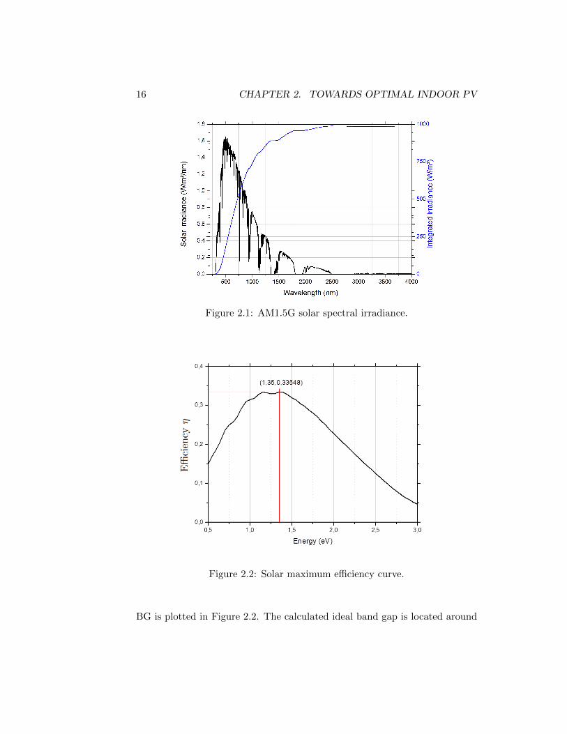
The solar spectrum (AM1.5G) is taken from the NREL data base avail-able online [12] and represented on Figure 2.1. The integral of the curve is1000 W.m−2.
A Mathematica code added in Appendix A solves Equation 12 using Equa-tion 9 and the maximal efficiency as a function of BG is derived from Equa-tion 13. The maximum efficiency curve for solar spectrum as a function of
16 CHAPTER 2. TOWARDS OPTIMAL INDOOR PV
Figure 2.1: AM1.5G solar spectral irradiance.
Figure 2.2: Solar maximum efficiency curve.
BG is plotted in Figure 2.2. The calculated ideal band gap is located around
2.3. APPLICATION TO LED SPECTRUM 17
1.35 eV and corresponds to a 33.5% power conversion efficiency (PCE) whichis consistent with the 33% limit.
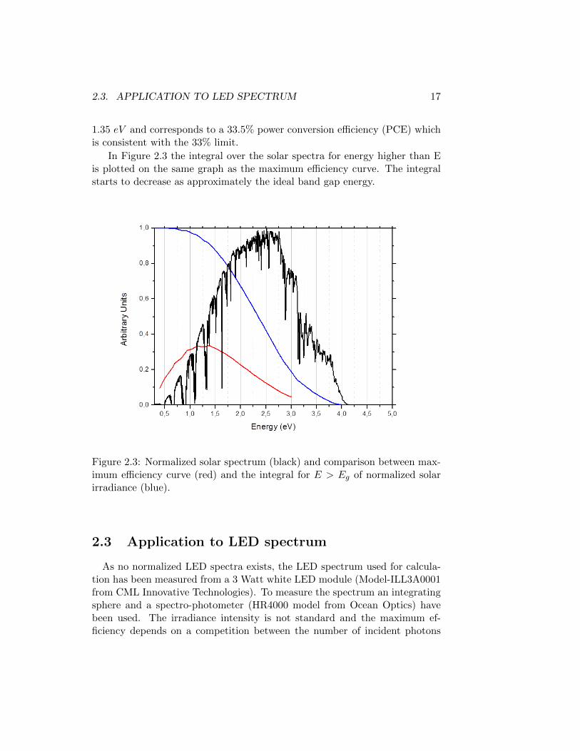
In Figure 2.3 the integral over the solar spectra for energy higher than Eis plotted on the same graph as the maximum efficiency curve. The integralstarts to decrease as approximately the ideal band gap energy.
Figure 2.3: Normalized solar spectrum (black) and comparison between max-imum efficiency curve (red) and the integral for E > Eg of normalized solarirradiance (blue).
2.3 Application to LED spectrum
As no normalized LED spectra exists, the LED spectrum used for calcula-tion has been measured from a 3 Watt white LED module (Model-ILL3A0001from CML Innovative Technologies). To measure the spectrum an integratingsphere and a spectro-photometer (HR4000 model from Ocean Optics) havebeen used. The irradiance intensity is not standard and the maximum ef-ficiency depends on a competition between the number of incident photons
18 CHAPTER 2. TOWARDS OPTIMAL INDOOR PV
above the BG and the recombination rate. The maximum efficiency value willdepend on the incoming intensity, however the maximum location (in eV) willremain the same.
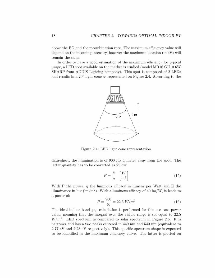
In order to have a good estimation of the maximum efficiency for typicalusage, a LED spot available on the market is studied (model MR16 GU10 6WSHARP from ADDIS Lighting company). This spot is composed of 2 LEDsand results in a 20 light cone as represented on Figure 2.4. According to the
Figure 2.4: LED light cone representation.
data-sheet, the illumination is of 900 lux 1 meter away from the spot. Thelatter quantity has to be converted as follow:
P =E
η
[W
m2
](15)
With P the power, η the luminous efficacy in lumens per Watt and E theilluminance in lux (lm/m2). With a luminous efficacy of 40 lm/W, it leads toa power of:
P =900
40= 22.5 W/m2 (16)
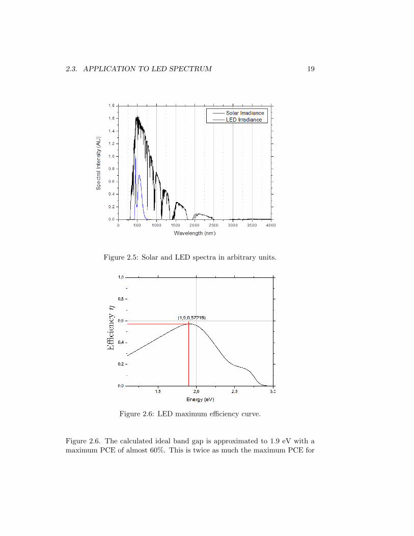
The ideal indoor band gap calculation is performed for this use case powervalue, meaning that the integral over the visible range is set equal to 22.5W/m2. LED spectrum is compared to solar spectrum in Figure 2.5. It isnarrower and has a two peaks centered in 449 nm and 540 nm (equivalent to2.77 eV and 2.28 eV respectively). This specific spectrum shape is expectedto be identified in the maximum efficiency curve. The latter is plotted on
2.3. APPLICATION TO LED SPECTRUM 19
Figure 2.5: Solar and LED spectra in arbitrary units.
Figure 2.6: LED maximum efficiency curve.
Figure 2.6. The calculated ideal band gap is approximated to 1.9 eV with amaximum PCE of almost 60%. This is twice as much the maximum PCE for
20 CHAPTER 2. TOWARDS OPTIMAL INDOOR PV
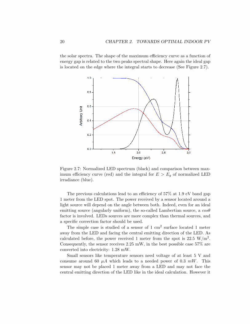
the solar spectra. The shape of the maximum efficiency curve as a function ofenergy gap is related to the two peaks spectral shape. Here again the ideal gapis located on the edge where the integral starts to decrease (See Figure 2.7).
Figure 2.7: Normalized LED spectrum (black) and comparison between max-imum efficiency curve (red) and the integral for E > Eg of normalized LEDirradiance (blue).
The previous calculations lead to an efficiency of 57% at 1.9 eV band gap1 meter from the LED spot. The power received by a sensor located around alight source will depend on the angle between both. Indeed, even for an idealemitting source (angularly uniform), the so-called Lambertian source, a cosθfactor is involved. LEDs sources are more complex than thermal sources, anda specific correction factor should be used.
The simple case is studied of a sensor of 1 cm2 surface located 1 meteraway from the LED and facing the central emitting direction of the LED. Ascalculated before, the power received 1 meter from the spot is 22.5 W/m2.Consequently, the sensor receives 2.25 mW, in the best possible case 57% areconverted into electricity: 1.28 mW.
Small sensors like temperature sensors need voltage of at least 5 V andconsume around 60 µA which leads to a needed power of 0.3 mW . Thissensor may not be placed 1 meter away from a LED and may not face thecentral emitting direction of the LED like in the ideal calculation. However it

2.3. APPLICATION TO LED SPECTRUM 21
probably receives light from several light sources (2 or more LEDs and outsidesun light through windows). We conclude that supplying indoor small sensorswith photovoltaic effect is possible.
Chapter 3
Design of a planarPerovskites-basedphotovoltaics device
In this chapter, indoor PV cell design is investigated. We examine Per-ovskites as the active layer. The complete planar device is considered.
3.1 Introduction to Perovskites
History
High efficiency dye-sentitized solar cell (DSSCs) also called Gratzel cellswere developped by M. Gratzel & B. O’Regan in 1991 at EPFL in Switzerland[13]. This organic thin film cell consists of a photo-electrochemical system anda mesoporous architecture.
In parallel, PVK was studied by D. Mitzi at IBM for LEDs applications(green emission)[14]. At that time PVK was not considered for solar applica-tions because of stability issues and Lead toxicity.
More than ten years later, in 2009, Miyasaka et al [15] incorporated PVKin DSSCs with a liquid electrolyte. They reached 3,8% PCE but the cell wasvery unstable, the liquid electrolyte dissolved away the Perovskite crystallinitywithin a few minutes.
The stability problem was solved in 2012 by H. Snaith and M. Lee fromOxford University. They stated that PVK are stable when used with a solidhole-transport material so-called Spiro-OMeTAD. Since then the architectureof PVK based solar cells was based on Gratzel cells’s mesoporous structure.
22
3.1. INTRODUCTION TO PEROVSKITES 23
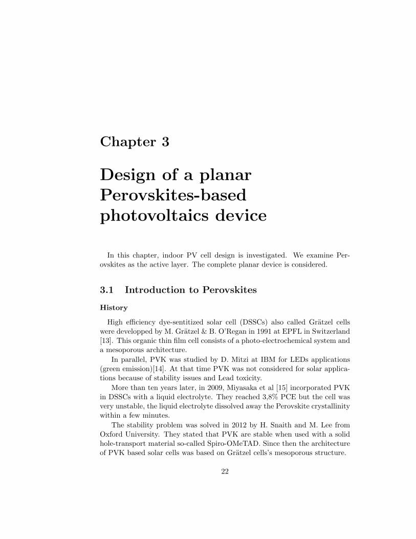
In 2014 H. Snaith et al deleted the mesoporous structure and introduceplanar structures with a PCE above 10% [16]. Nowadays, both structuresexist. They are drawn in Figure 3.1.
Figure 3.1: Perovskite cell structures: planar structure without scaffold andmesoporous structure with scaffold.
Research on this topic is going on and most recently, 20% PCE cell hasbeen confirmed by NREL (See Figure 1.1).
Structure
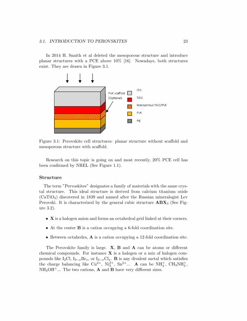
The term ”Pervoskites” designates a family of materials with the same crys-tal structure. This ideal structure is derived from calcium titanium oxide(CaTiO3) discovered in 1839 and named after the Russian mineralogist LevPerovski. It is characterized by the general cubic structure ABX3 (See Fig-ure 3.2).
• X is a halogen anion and forms an octahedral grid linked at their corners.
• At the center B is a cation occupying a 6-fold coordination site.
• Between octahedra, A is a cation occupying a 12-fold coordination site.
The Perovskite family is large. X, B and A can be atoms or differentchemical compounds. For instance X is a halogen or a mix of halogen com-pounds like I2Cl, I3−xBrx, or I3−xClx. B is any divalent metal which satisfiesthe charge balancing like Cu2+, Ni2+2 , Sn2+... A can be NH+
4 , CH3NH+3 ,
NH3OH+... The two cations, A and B have very different sizes.
24CHAPTER 3. DESIGN OF A PLANAR PEROVSKITES-BASED
PHOTOVOLTAICS DEVICE
Figure 3.2: Ideal crystal structure of perovskite materials [16].
Technology and processes
Manufacturing processes are important to consider. Indeed the cell hasto be low-cost. Fortunately, Perovskites can be simple and cheap to producedepending on the process used, especially CH3NH3PbI3. Four general methodsto prepare this active layer exist: One-Step Precursor Deposition (OSPD),Sequential Deposition Method (SDM), Dual-Source Vapor Deposition (DSVD)or Vapor-Assisted Solution Process (VASP).
Liquid-phase processes are simpler, faster and cheaper for mass production,but water always remains and may dissolve Perovskite and decreases PCE.Evaporation processes are more expensive and more difficult to obtain but nowater remains and the crystallinity is maintained.
Light harvesting properties
The major advantage of Perovskites for PV is its huge absorption. Itsabsorption coefficient α exceeds 105 cm−1 over a wide range of wavelengths(which is ten times c-Si absorption coefficient). Consequently only a smallamount of material is needed. Thanks to flexibility, Perovskites are suitablefor thin film solar cells.
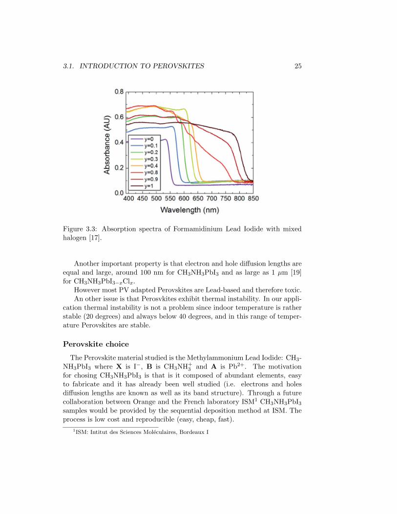
Another advantage is that despite their organic composition, Perovskitesbehave like semiconductors and not like organic materials [17]. Once a pho-ton is absorbed by the material, the electron-hole pair separates itself withoutany secondary process (unlike in organic solar cells). More precisely, Per-ovskites behave like a direct band-gap semiconductors whose gap is eventunable. As an example, mixing I with Br in Formamidinium Lead Iodide(CH(NH2)2PbIyBr3y) tunes the gap between 1.48 and 2.23 eV [18] as shownin Figure 3.3.
3.1. INTRODUCTION TO PEROVSKITES 25
Figure 3.3: Absorption spectra of Formamidinium Lead Iodide with mixedhalogen [17].
Another important property is that electron and hole diffusion lengths areequal and large, around 100 nm for CH3NH3PbI3 and as large as 1 µm [19]for CH3NH3PbI3−xClx.
However most PV adapted Perovskites are Lead-based and therefore toxic.An other issue is that Perosvkites exhibit thermal instability. In our appli-
cation thermal instability is not a problem since indoor temperature is ratherstable (20 degrees) and always below 40 degrees, and in this range of temper-ature Perovskites are stable.
Perovskite choice
The Perovskite material studied is the Methylammonium Lead Iodide: CH3-NH3PbI3 where X is I−, B is CH3NH+
3 and A is Pb2+. The motivationfor chosing CH3NH3PbI3 is that is it composed of abundant elements, easyto fabricate and it has already been well studied (i.e. electrons and holesdiffusion lengths are known as well as its band structure). Through a futurecollaboration between Orange and the French laboratory ISM1 CH3NH3PbI3samples would be provided by the sequential deposition method at ISM. Theprocess is low cost and reproducible (easy, cheap, fast).
1ISM: Intitut des Sciences Moleculaires, Bordeaux I
26CHAPTER 3. DESIGN OF A PLANAR PEROVSKITES-BASED
PHOTOVOLTAICS DEVICE
In the remainder of this thesis, PVK refers to CH3NH3PbI3.
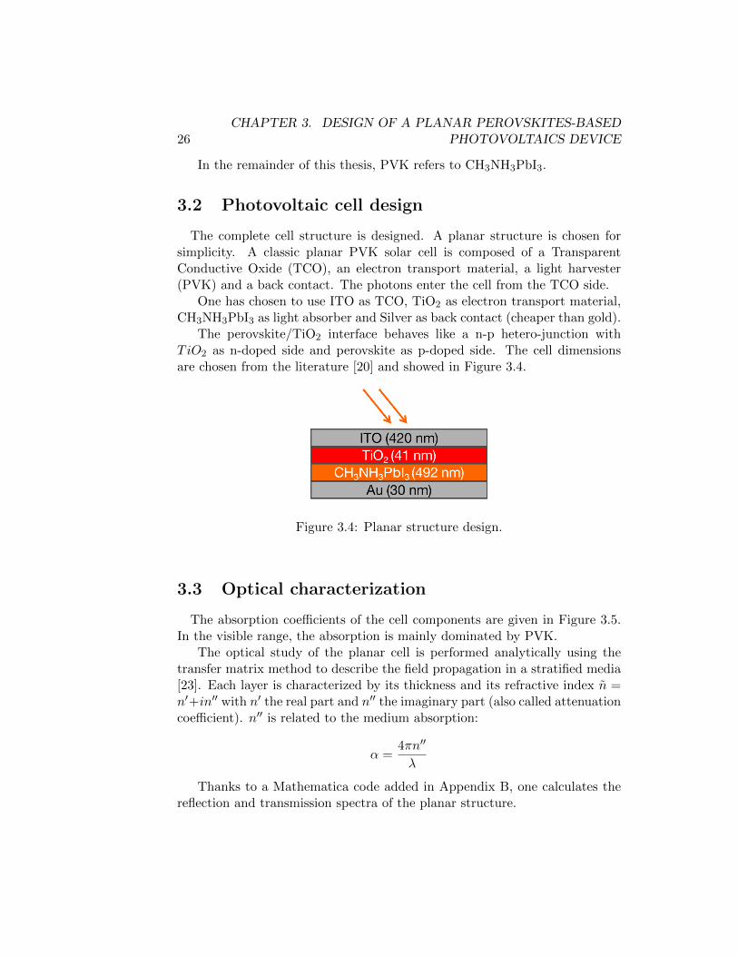
3.2 Photovoltaic cell design
The complete cell structure is designed. A planar structure is chosen forsimplicity. A classic planar PVK solar cell is composed of a TransparentConductive Oxide (TCO), an electron transport material, a light harvester(PVK) and a back contact. The photons enter the cell from the TCO side.
One has chosen to use ITO as TCO, TiO2 as electron transport material,CH3NH3PbI3 as light absorber and Silver as back contact (cheaper than gold).
The perovskite/TiO2 interface behaves like a n-p hetero-junction withTiO2 as n-doped side and perovskite as p-doped side. The cell dimensionsare chosen from the literature [20] and showed in Figure 3.4.
Figure 3.4: Planar structure design.
3.3 Optical characterization
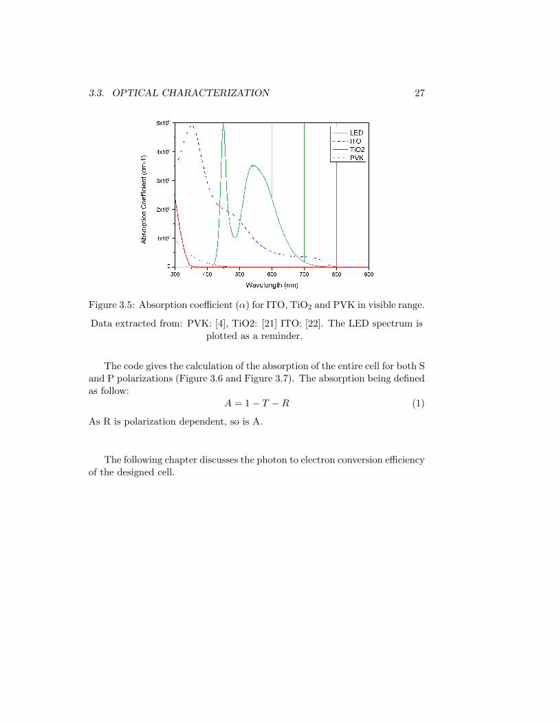
The absorption coefficients of the cell components are given in Figure 3.5.In the visible range, the absorption is mainly dominated by PVK.
The optical study of the planar cell is performed analytically using thetransfer matrix method to describe the field propagation in a stratified media[23]. Each layer is characterized by its thickness and its refractive index n =n′+in′′ with n′ the real part and n′′ the imaginary part (also called attenuationcoefficient). n′′ is related to the medium absorption:
α =4πn′′
λ
Thanks to a Mathematica code added in Appendix B, one calculates thereflection and transmission spectra of the planar structure.
3.3. OPTICAL CHARACTERIZATION 27
Figure 3.5: Absorption coefficient (α) for ITO, TiO2 and PVK in visible range.
Data extracted from: PVK: [4], TiO2: [21] ITO: [22]. The LED spectrum isplotted as a reminder.
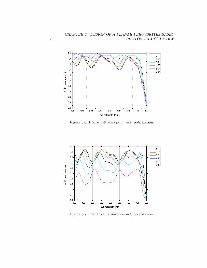
The code gives the calculation of the absorption of the entire cell for both Sand P polarizations (Figure 3.6 and Figure 3.7). The absorption being definedas follow:
A = 1− T −R (1)
As R is polarization dependent, so is A.
The following chapter discusses the photon to electron conversion efficiencyof the designed cell.
28CHAPTER 3. DESIGN OF A PLANAR PEROVSKITES-BASED
PHOTOVOLTAICS DEVICE
Figure 3.6: Planar cell absorption in P polarization.
Figure 3.7: Planar cell absorption in S polarization.
Chapter 4
Planar cell quantum efficiency
The previous cell structure can be improved by adding a hole transportmaterial (HTM). The generated photocurrent inside two structures are inves-tigated: a TiO2/PVK junction and a TiO2/PVK/HTM junction. Accordingto the litterature, the first junction is treated as a n-p junction [24], the otherone is treated as a n-i-p junction [25].
4.1 Heterojunction QE calculation
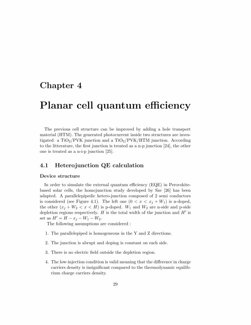
Device structure
In order to simulate the external quantum efficiency (EQE) in Perovskite-based solar cells, the homojunction study developed by Sze [26] has beenadapted. A parallelepipedic hetero-junction composed of 2 semi conductorsis considered (see Figure 4.1). The left one (0 < x < xj + W1) is n-doped,the other (xj + W2 < x < H) is p-doped. W1 and W2 are n-side and p-sidedepletion regions respectively. H is the total width of the junction and H ′ isset as H ′ = H − xj −W1 −W2.
The following assumptions are considered :
1. The parallelepiped is homogeneous in the Y and Z directions.
2. The junction is abrupt and doping is constant on each side.
3. There is no electric field outside the depletion region.
4. The low-injection condition is valid meaning that the difference in chargecarriers density is insignificant compared to the thermodynamic equilib-rium charge carriers density.
29
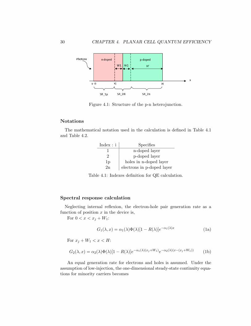
30 CHAPTER 4. PLANAR CELL QUANTUM EFFICIENCY
Figure 4.1: Structure of the p-n heterojunction.
Notations
The mathematical notation used in the calculation is defined in Table 4.1and Table 4.2.
Index : i Specifies
1 n-doped layer2 p-doped layer
1p holes in n-doped layer2n electrons in p-doped layer
Table 4.1: Indexes definition for QE calculation.
Spectral response calculation
Neglecting internal reflexion, the electron-hole pair generation rate as afunction of position x in the device is,
For 0 < x < xj +W1:
G1(λ, x) = α1(λ)Φ(λ)[1−R(λ)]e−α1(λ)x (1a)
For xj +W1 < x < H:
G2(λ, x) = α2(λ)Φ(λ)[1−R(λ)]e−α1(λ)(xj+W1)e−α2(λ)(x−(xj+W1)) (1b)
An equal generation rate for electrons and holes is assumed. Under theassumption of low-injection, the one-dimensional steady-state continuity equa-tions for minority carriers becomes
4.1. HETEROJUNCTION QE CALCULATION 31
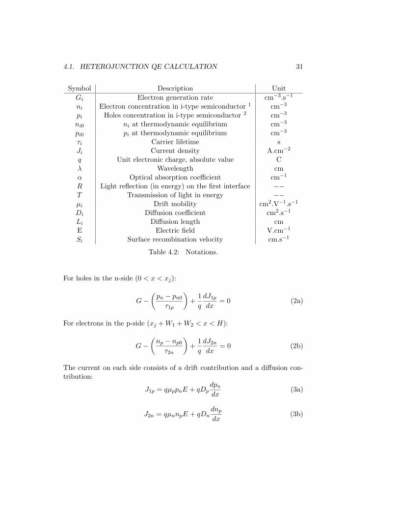
Symbol Description Unit
Gi Electron generation rate cm−3.s−1
ni Electron concentration in i-type semiconductor 1 cm−3
pi Holes concentration in i-type semiconductor 2 cm−3
ni0 ni at thermodynamic equilibrium cm−3
pi0 pi at thermodynamic equilibrium cm−3
τi Carrier lifetime sJi Current density A.cm−2
q Unit electronic charge, absolute value Cλ Wavelength cmα Optical absorption coefficient cm−1
R Light reflection (in energy) on the first interface −−T Transmission of light in energy −−µi Drift mobility cm2.V−1.s−1
Di Diffusion coefficient cm2.s−1
Li Diffusion length cmE Electric field V.cm−1
Si Surface recombination velocity cm.s−1
Table 4.2: Notations.
For holes in the n-side (0 < x < xj):
G−(pn − pn0τ1p
)+
1
q
dJ1pdx
= 0 (2a)
For electrons in the p-side (xj +W1 +W2 < x < H):
G−(np − np0τ2n
)+
1
q
dJ2ndx
= 0 (2b)
The current on each side consists of a drift contribution and a diffusion con-tribution:
J1p = qµppnE + qDpdpndx
(3a)
J2n = qµnnpE + qDndnpdx
(3b)
32 CHAPTER 4. PLANAR CELL QUANTUM EFFICIENCY
N-side photocurrent: For the n-side of the junction, Equation 1b, Equa-tion 2b and Equation 3b yield to :
D1pd2p2ndx2
+ α1Φ(1−R)e−α1x − pn − pn0τ1p
= 0 (4)
Introducing the diffusion length Lp =√Dpτp, the general solution to the
system is:
pn − pn0 = C2 cosh
(x
L1p
)+ C3 sinh
(x
L1p
)− α1Φ(1−R)τ1p
α12L1p
2 − 1(5)
C2 and C3 are determined using the boundary conditions :
• At the surface (x = 0), the surface recombination is Sp
• At the depletion edge (x = xj), the excess carrier density is small dueto the electric field in the depletion region
The N-side photocurrent is derived using Equation 5 and Equation 3bevaluated at the depletion edge:
(J1p)xj = −qD1p
(dpndx
)xj
(6)
=qΦ(1−R)α1L1p
α12L1p
2 − 1×
(S1pL1p
D1p+ α1L1p)− e−α1xj (
S1pL1p
D1pcosh(
xjL1p
) + sinh(xjL1p
))
S1pL1p
D1psinh(
xjL1p
) + cosh(xjL1p
)− α1L1pe
−α1xj
(J1p)xj is the n-side contribution to photocurrent.
P-side photocurrent Similar calculations can be done for Jn in the rightp-side using Equation 1b, Equation 2a and Equation 3a and the boundaryconditions:
• At x = H, the surface recombination is Sn.
• At x = xj +W1 +W2, the excess carrier density is small.
4.1. HETEROJUNCTION QE CALCULATION 33
(J2n)xj+W1+W2 = −qD2n
(dnpdx
)xj+W1+W2
(7)
=qΦ(1−R)α2L2n
α22L2n
2 − 1e−α2W2−α1(xj+W1)×
α2L2n −S2nL2nD2n
(cosh( H′L2n− e−α2H′)) + sinh( H′
L2n− e−α2H′) + α2L2ne
−α2H′
S2nL2nD2n
sinh( H′L2n
) + cosh( H′L2n
)
(J2n)xj+W1+W2 is the p-side contribution to photocurrent.
Depletion region photo-current: In the depletion region the carrier lifetime is considered to be infinite, assuming no recombination process. Westill consider that there is no electric field at the depletion edge, then thephotogenerated photo-current is given by:
JDR = q
∫ xj+W1
xj
G1(λ, x) dx+ q
∫ xj+W1
xj+W1+W2
G2(λ, x) dx (8)
= qΦ(1−R)[e−α1xj (1− e−α1W1) + e−α1(xj+W1)(e−α2W2 − 1)
]
Quantum efficiency The spectral response is obtained by summing thecontribution from each of the three regions:
QE1 =(J1p)xj
qΦ(1−R)(9)
QE2 =(J2n)xj+W1+W2
qΦ(1−R)(10)
QEDR1,2 =(JDR)
qΦ(1−R)(11)
Finally only the design parameters and the physical parameters: αi, Li, Di
and Si are needed to obtain the QE of a p-n heterojunction.
34 CHAPTER 4. PLANAR CELL QUANTUM EFFICIENCY
4.2 N-P heterojunction structure
Device structure
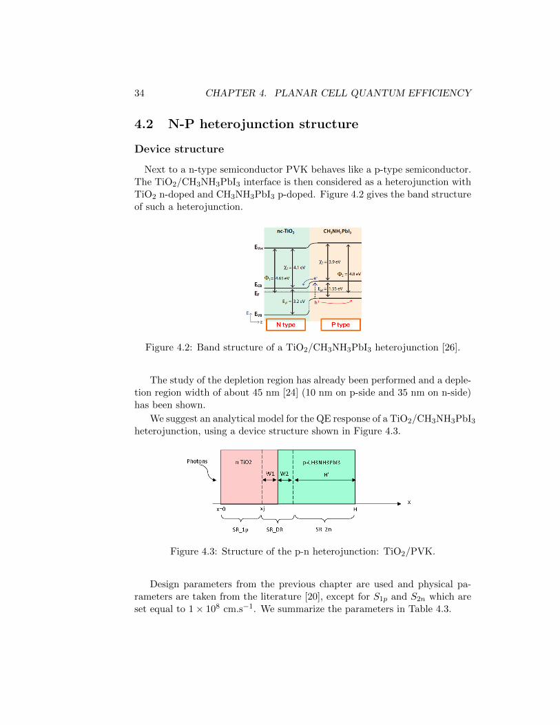
Next to a n-type semiconductor PVK behaves like a p-type semiconductor.The TiO2/CH3NH3PbI3 interface is then considered as a heterojunction withTiO2 n-doped and CH3NH3PbI3 p-doped. Figure 4.2 gives the band structureof such a heterojunction.
Figure 4.2: Band structure of a TiO2/CH3NH3PbI3 heterojunction [26].
The study of the depletion region has already been performed and a deple-tion region width of about 45 nm [24] (10 nm on p-side and 35 nm on n-side)has been shown.
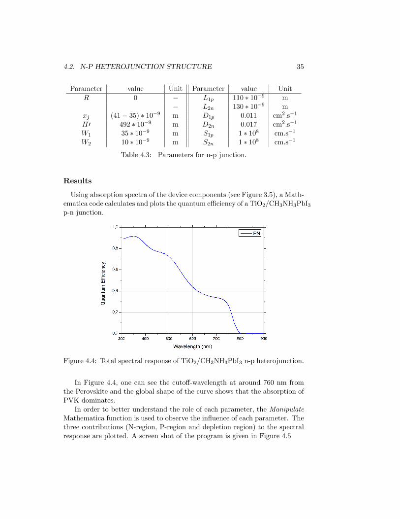
We suggest an analytical model for the QE response of a TiO2/CH3NH3PbI3heterojunction, using a device structure shown in Figure 4.3.
Figure 4.3: Structure of the p-n heterojunction: TiO2/PVK.
Design parameters from the previous chapter are used and physical pa-rameters are taken from the literature [20], except for S1p and S2n which areset equal to 1× 108 cm.s−1. We summarize the parameters in Table 4.3.
4.2. N-P HETEROJUNCTION STRUCTURE 35
Parameter value Unit Parameter value Unit
R 0 − L1p 110 ∗ 10−9 m− L2n 130 ∗ 10−9 m
xj (41− 35) ∗ 10−9 m D1p 0.011 cm2.s−1
H′ 492 ∗ 10−9 m D2n 0.017 cm2.s−1
W1 35 ∗ 10−9 m S1p 1 ∗ 108 cm.s−1
W2 10 ∗ 10−9 m S2n 1 ∗ 108 cm.s−1
Table 4.3: Parameters for n-p junction.
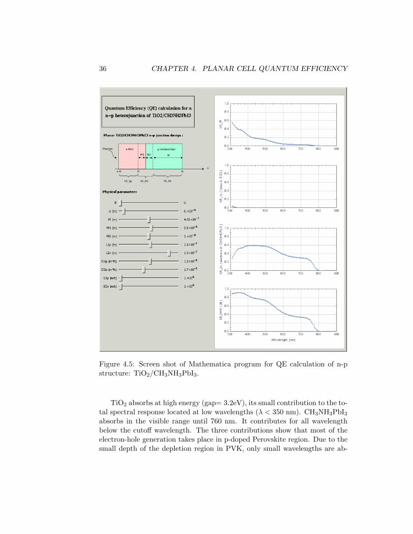
Results
Using absorption spectra of the device components (see Figure 3.5), a Math-ematica code calculates and plots the quantum efficiency of a TiO2/CH3NH3PbI3p-n junction.
Figure 4.4: Total spectral response of TiO2/CH3NH3PbI3 n-p heterojunction.
In Figure 4.4, one can see the cutoff-wavelength at around 760 nm fromthe Perovskite and the global shape of the curve shows that the absorption ofPVK dominates.
In order to better understand the role of each parameter, the ManipulateMathematica function is used to observe the influence of each parameter. Thethree contributions (N-region, P-region and depletion region) to the spectralresponse are plotted. A screen shot of the program is given in Figure 4.5
36 CHAPTER 4. PLANAR CELL QUANTUM EFFICIENCY
Figure 4.5: Screen shot of Mathematica program for QE calculation of n-pstructure: TiO2/CH3NH3PbI3.
TiO2 absorbs at high energy (gap= 3.2eV), its small contribution to the to-tal spectral response located at low wavelengths (λ < 350 nm). CH3NH3PbI3absorbs in the visible range until 760 nm. It contributes for all wavelengthbelow the cutoff wavelength. The three contributions show that most of theelectron-hole generation takes place in p-doped Perovskite region. Due to thesmall depth of the depletion region in PVK, only small wavelengths are ab-
4.3. N-I-P HETEROJUNCTION STRUCTURE 37
sorbed (corresponding to high α). Expanding W2 leads to higher depletionregion contribution.
The ratio of the diffusion length to device dimension influences the QE.Both electron and hole diffusion lengths would preferably be larger than thedistance to the contacts.
4.3 N-I-P heterojunction structure
In order to enhance the cell performance, it is possible to add a hole trans-port material to the cell. The structure TiO2/CH3NH3PbI3/HTM then be-haves like a p-i-n hetero-junction. The QE simulation of a TiO2/CH3NH3PbI3/-SpiroOmeTAD is studied using previous calculation.
According to literature, PVK adopts the properties showed in Figure 4.6,where a part of the PVK is dominated by drift and a part by diffusion [25].
Figure 4.6: TiO2/CH3NH3PbI3/SpiroOmeTAD band structure [27].
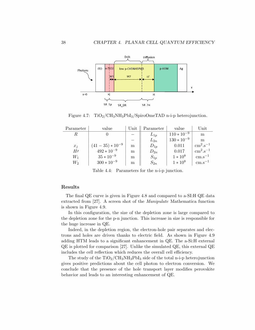
For QE calculation, one considers the n-TiO2/i-CH3NH3PbI3/p-CH3NH3PbI3junction. TiO2 is n-doped and CH3NH3PbI3 is separated in two regions: thedrifting (i-CH3NH3PbI3) and the diffusion regions (p-CH3NH3PbI3) (See Fig-ure 4.7). In the calculation the hole transport material is indirectly taken intoaccount since Perovskite behavior is related to HTM presence.
Device structure
The previous discussion leads us to consider the n-p junction between TiO2
and CH3NH3PbI3 with different physical parameters (see Table 4.4). AgainS1p and S2n are set equal to 1 ∗ 108 cm.s−1.
38 CHAPTER 4. PLANAR CELL QUANTUM EFFICIENCY
Figure 4.7: TiO2/CH3NH3PbI3/SpiroOmeTAD n-i-p heterojunction.
Parameter value Unit Parameter value Unit
R 0 − L1p 110 ∗ 10−9 m− L2n 130 ∗ 10−9 m
xj (41− 35) ∗ 10−9 m D1p 0.011 cm2.s−1
H′ 492 ∗ 10−9 m D2n 0.017 cm2.s−1
W1 35 ∗ 10−9 m S1p 1 ∗ 108 cm.s−1
W2 300 ∗ 10−9 m S2n 1 ∗ 108 cm.s−1
Table 4.4: Parameters for the n-i-p junction.
Results
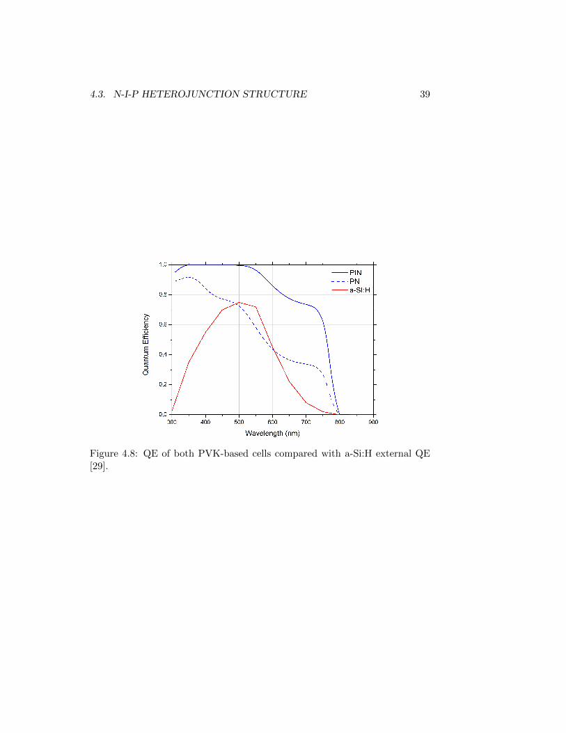
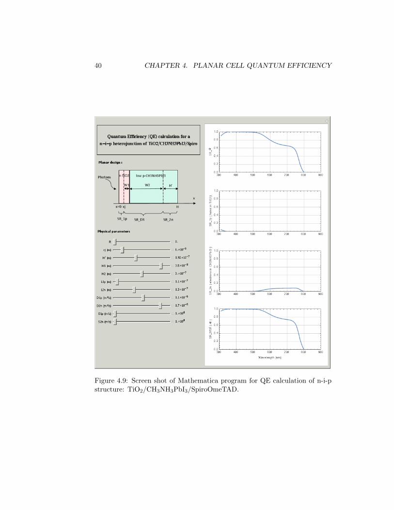
The final QE curve is given in Figure 4.8 and compared to a-SI:H QE dataextracted from [27]. A screen shot of the Manipulate Mathematica functionis shown in Figure 4.9.
In this configuration, the size of the depletion zone is large compared tothe depletion zone for the p-n junction. This increase in size is responsible forthe huge increase in QE.
Indeed, in the depletion region, the electron-hole pair separates and elec-trons and holes are driven thanks to electric field. As shown in Figure 4.9adding HTM leads to a significant enhancement in QE. The a-Si:H externalQE is plotted for comparison [27]. Unlike the simulated QE, this external QEincludes the cell reflection which reduces the overall cell efficiency.
The study of the TiO2/CH3NH3PbI3 side of the total n-i-p heterojunctiongives positive predictions about the cell photon to electron conversion. Weconclude that the presence of the hole transport layer modifies perovskitebehavior and leads to an interesting enhancement of QE.
4.3. N-I-P HETEROJUNCTION STRUCTURE 39
Figure 4.8: QE of both PVK-based cells compared with a-Si:H external QE[29].
40 CHAPTER 4. PLANAR CELL QUANTUM EFFICIENCY
Figure 4.9: Screen shot of Mathematica program for QE calculation of n-i-pstructure: TiO2/CH3NH3PbI3/SpiroOmeTAD.
Chapter 5
Photonic crystal towardshiger performances
In the following chapter, a photonic crystal structure to enhance the accep-tance angle of the cell is studied.
5.1 Introduction to photonic crystals
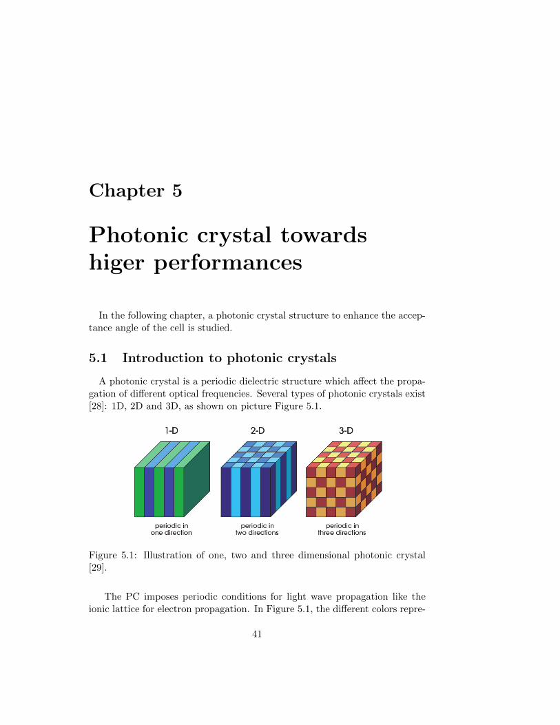
A photonic crystal is a periodic dielectric structure which affect the propa-gation of different optical frequencies. Several types of photonic crystals exist[28]: 1D, 2D and 3D, as shown on picture Figure 5.1.
Figure 5.1: Illustration of one, two and three dimensional photonic crystal[29].
The PC imposes periodic conditions for light wave propagation like theionic lattice for electron propagation. In Figure 5.1, the different colors repre-
41
42CHAPTER 5. PHOTONIC CRYSTAL TOWARDS HIGER
PERFORMANCES
sent different dielectric constants and the periodicity along one, two or threedirections define the type of PC. The photon propagation inside the crystalare determined by the lattice geometry and index contrast.
5.2 Photonic crystal choice
Motivation
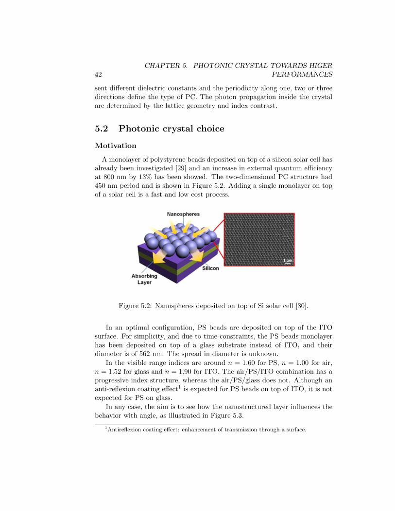
A monolayer of polystyrene beads deposited on top of a silicon solar cell hasalready been investigated [29] and an increase in external quantum efficiencyat 800 nm by 13% has been showed. The two-dimensional PC structure had450 nm period and is shown in Figure 5.2. Adding a single monolayer on topof a solar cell is a fast and low cost process.
Figure 5.2: Nanospheres deposited on top of Si solar cell [30].
In an optimal configuration, PS beads are deposited on top of the ITOsurface. For simplicity, and due to time constraints, the PS beads monolayerhas been deposited on top of a glass substrate instead of ITO, and theirdiameter is of 562 nm. The spread in diameter is unknown.
In the visible range indices are around n = 1.60 for PS, n = 1.00 for air,n = 1.52 for glass and n = 1.90 for ITO. The air/PS/ITO combination has aprogressive index structure, whereas the air/PS/glass does not. Although ananti-reflexion coating effect1 is expected for PS beads on top of ITO, it is notexpected for PS on glass.
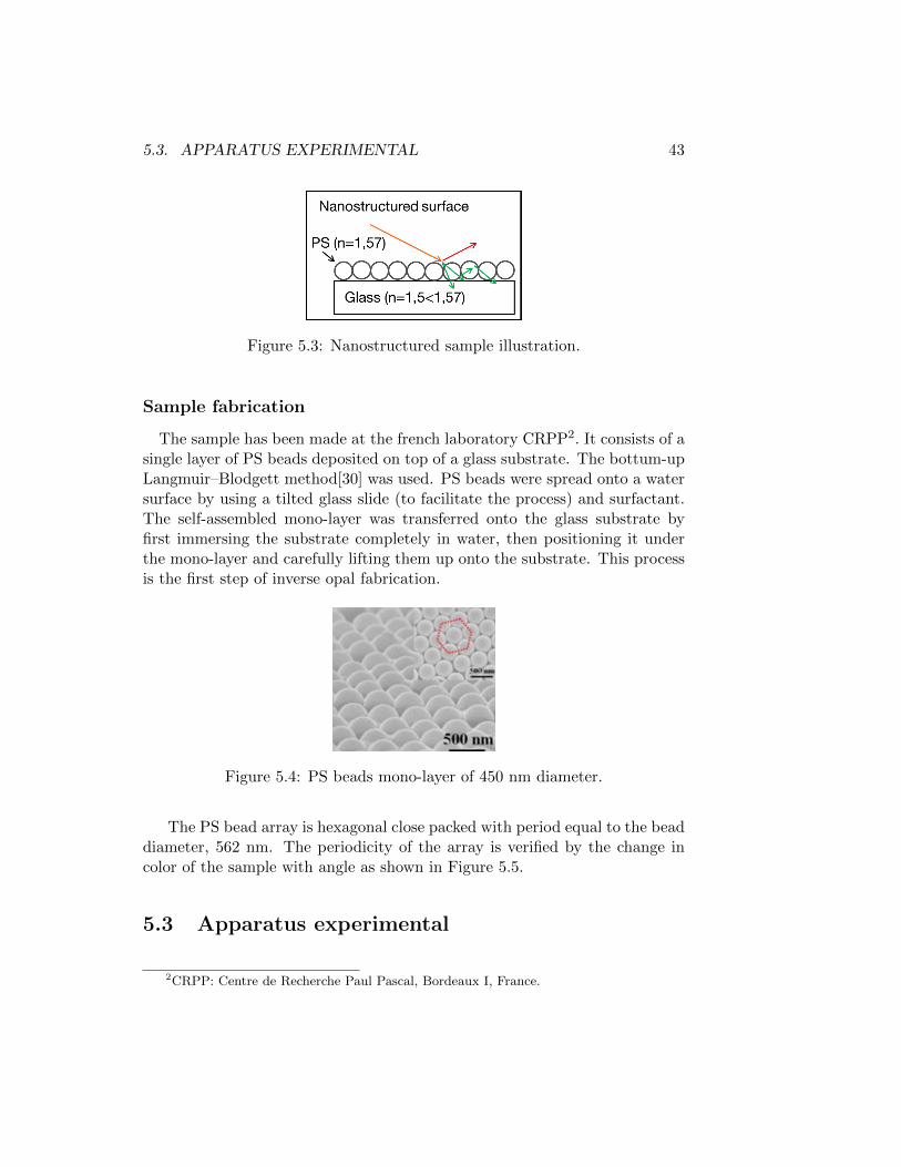
In any case, the aim is to see how the nanostructured layer influences thebehavior with angle, as illustrated in Figure 5.3.
1Antireflexion coating effect: enhancement of transmission through a surface.
5.3. APPARATUS EXPERIMENTAL 43
Figure 5.3: Nanostructured sample illustration.
Sample fabrication
The sample has been made at the french laboratory CRPP2. It consists of asingle layer of PS beads deposited on top of a glass substrate. The bottum-upLangmuir–Blodgett method[30] was used. PS beads were spread onto a watersurface by using a tilted glass slide (to facilitate the process) and surfactant.The self-assembled mono-layer was transferred onto the glass substrate byfirst immersing the substrate completely in water, then positioning it underthe mono-layer and carefully lifting them up onto the substrate. This processis the first step of inverse opal fabrication.
Figure 5.4: PS beads mono-layer of 450 nm diameter.
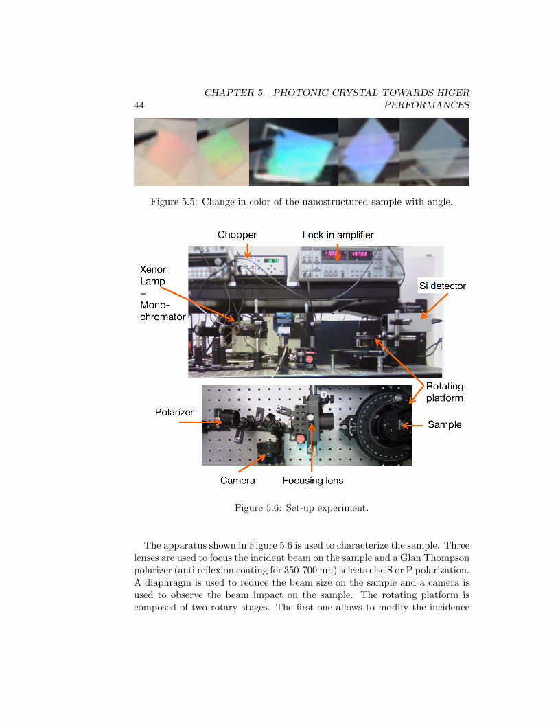
The PS bead array is hexagonal close packed with period equal to the beaddiameter, 562 nm. The periodicity of the array is verified by the change incolor of the sample with angle as shown in Figure 5.5.
5.3 Apparatus experimental
2CRPP: Centre de Recherche Paul Pascal, Bordeaux I, France.
44CHAPTER 5. PHOTONIC CRYSTAL TOWARDS HIGER
PERFORMANCES
Figure 5.5: Change in color of the nanostructured sample with angle.
Figure 5.6: Set-up experiment.
The apparatus shown in Figure 5.6 is used to characterize the sample. Threelenses are used to focus the incident beam on the sample and a Glan Thompsonpolarizer (anti reflexion coating for 350-700 nm) selects else S or P polarization.A diaphragm is used to reduce the beam size on the sample and a camera isused to observe the beam impact on the sample. The rotating platform iscomposed of two rotary stages. The first one allows to modify the incidence
5.4. FINITE DIFFERENCE TIME DOMAIN METHOD 45
angle on the sample and the second one allows the detector to turn around thesample and collect the reflected or transmitted beam. Due to constraints withthe size of the detector, angles smaller than θmin = 20 can not be measured.
5.4 Finite Difference Time Domain method
OptiFDTD numerical software (from Optiwave company) is used in orderto simulate experimental results and to simulate PS beads on top of ITO.Simulator is numerical. Indeed, analytical model does not exist for 2D and3D nanostructured materials.
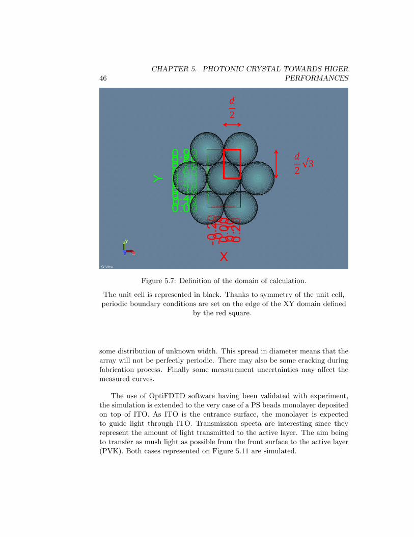
The FDTD directly solves the time dependent Maxwell’s curl equations.The calculation can be performed on 2D or 3D meshes. Calculations are slow,so it is convenient to reduce the domain as much as possible. Boundary con-ditions are defined: anisotropic perfectly matched layers boundary conditionsare applied on the edge of the computational window in the propagation di-rection and periodic conditions are used in the nanostructured plane to reducethe domain to a single unit cell. Figure 5.7 shows the defined pattern.
In order to perform a simulation, an input plane has to be defined to set thespectral range of calculation. Many designs and shapes can be created withOptiFDTD but the important point is to correctly define the media indices.OptiFDTD allows for different media but they must be well described by aSellmeier model or a modified Lorentz-Drude model. The modeled materialsand their optical properties are detailed in Appendix C.
5.5 Experimental results and comparison withsimulations
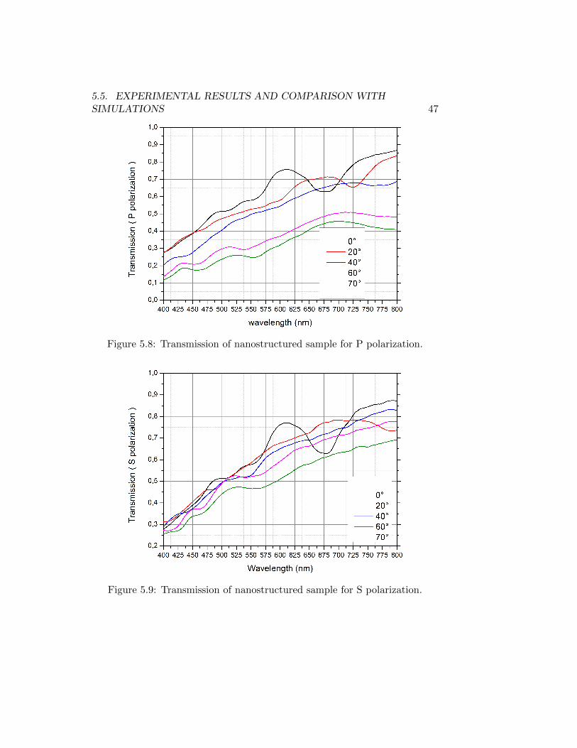
The measured transmission of the nanostructured surface is plotted for bothpolarizations (See Figure 5.8 and Figure 5.9). The curves have been smoothedto observe the general behavior. Global transmission decreases with angle forboth polarizations and local resonances are observed.
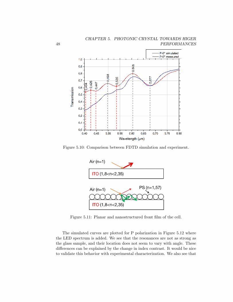
In order to validate the use of OptiFDTD software, the simulation of thetransmission in P polarization at 0 is done. The comparison between exper-iment and simulation is given on Figure 5.10. Comparing both curves, onecan see that resonances at around 500 nm, 600 nm and 680 nm are present inboth curves. However the general slope of the curves does not exactly match.There are several reasons for this discrepancy. The bead diameter is assumedto be 562 nm but this quantity has some experimental uncertainty. The diam-eter is assumed to be the same for all deposited beads but in reality there is
46CHAPTER 5. PHOTONIC CRYSTAL TOWARDS HIGER
PERFORMANCES
Figure 5.7: Definition of the domain of calculation.
The unit cell is represented in black. Thanks to symmetry of the unit cell,periodic boundary conditions are set on the edge of the XY domain defined
by the red square.
some distribution of unknown width. This spread in diameter means that thearray will not be perfectly periodic. There may also be some cracking duringfabrication process. Finally some measurement uncertainties may affect themeasured curves.
The use of OptiFDTD software having been validated with experiment,the simulation is extended to the very case of a PS beads monolayer depositedon top of ITO. As ITO is the entrance surface, the monolayer is expectedto guide light through ITO. Transmission specta are interesting since theyrepresent the amount of light transmitted to the active layer. The aim beingto transfer as mush light as possible from the front surface to the active layer(PVK). Both cases represented on Figure 5.11 are simulated.
5.5. EXPERIMENTAL RESULTS AND COMPARISON WITHSIMULATIONS 47
Figure 5.8: Transmission of nanostructured sample for P polarization.
Figure 5.9: Transmission of nanostructured sample for S polarization.
48CHAPTER 5. PHOTONIC CRYSTAL TOWARDS HIGER
PERFORMANCES
Figure 5.10: Comparison between FDTD simulation and experiment.
Figure 5.11: Planar and nanostructured front film of the cell.
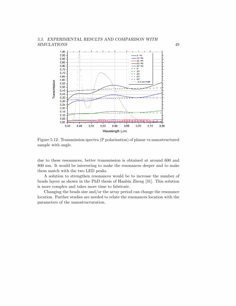
The simulated curves are plotted for P polarization in Figure 5.12 wherethe LED spectrum is added. We see that the resonances are not as strong asthe glass sample, and their location does not seem to vary with angle. Thesedifferences can be explained by the change in index contrast. It would be niceto validate this behavior with experimental characterization. We also see that
5.5. EXPERIMENTAL RESULTS AND COMPARISON WITHSIMULATIONS 49
Figure 5.12: Transmission spectra (P polarization) of planar vs nanostructuredsample with angle.
due to these resonances, better transmission is obtained at around 600 and800 nm. It would be interesting to make the resonances deeper and to makethem match with the two LED peaks.
A solution to strengthen resonances would be to increase the number ofbeads layers as shown in the PhD thesis of Hanbin Zheng [31]. This solutionis more complex and takes more time to fabricate.
Changing the beads size and/or the array period can change the resonancelocation. Further studies are needed to relate the resonances location with theparameters of the nanostructuration.
Chapter 6
Conclusion and perspectives
This work makes three contributions to the development of high efficiencyPerovskites-based photovoltaic cell ’adapted to indoor environment’. An es-timate of how much power can be harvested from LED illumination is givenand the conclusion is that it is enough to supply low power sensors. A studyof PVK shows that it has a quantum efficiency close to 1 over visible rangewhen using a hole transport material. Moreover its low cost of productionmakes it well adapted to IoT applications. Finally, a study of nanostructuringthe surface of a solar cell has been done. The deposition of a Polystyrene beadmonolayer on top of the front surface does not seem to enhance the transmis-sion through the front surface. Further studies are needed to understand howthe nanostructured array affects the photon motion and solar cell efficiency.
50
Bibliography
[1] S. Guha, J. Yang, and B. Yan. 6.08 - amorphous and nanocrystallinesilicon solar cells and modules. In P. Bhattacharya, R. Fornari, andKamimura H., editors, Comprehensive Semiconductor Science and Tech-nology, pages 308 – 352. Elsevier, Amsterdam, 2011.
[2] J. Nelson. The physics of solar cells, volume 1. World Scientific, 2003.
[3] J. Burschka, N. Pellet, S.-J. Moon, R. Humphry-Baker, P. Gao, M. K.Nazeeruddin, and M. Gratzel. Sequential deposition as a route to high-performance perovskite-sensitized solar cells. Nature, 499(7458):316–319,2013.
[4] P. Loper, M. Stuckelberger, B. Niesen, J. Werner, M. Filipic, S.-J. Moon,J.-H. Yum, M. Topic, S. De Wolf, and C. Ballif. Complex refractive indexspectra of ch3nh3pbi3 perovskite thin films determined by spectroscopicellipsometry and spectrophotometry. The Journal of Physical ChemistryLetters, 6(1):66–71, 2015.
[5] Perovskite solar cells 5x cheaper than comparable thin-film tech-nology. http://www.laserfocusworld.com/articles/2013/10/
perovskite-solar-cells-5x-cheaper-than-comparable-thin-film-technology.
html. Accessed: 2015-12-23.
[6] E. Yablonovitch. Inhibited spontaneous emission in solid-state physicsand electronics. Phys. Rev. Lett., 58(20):2059–2062, 1987.
[7] G. Gomard. Cristaux photoniques pour le controle de l’absorption dans lescellules solaires photovoltaıques silicium ultraminces. PhD thesis, EcoleCentrale Lyon, 2012.
[8] C.E. Bres. Etude optique de cellules photovoltaıques nanostructurees(cristaux photoniques 2d) a base de a-si :h optimisees pour l’alimentation
51

52 BIBLIOGRAPHY
de capteurs indoor, MA. thesis, Institut d’Optique Graduate School,2013.
[9] W. Shockley and H. J. Queisser. Detailed balance limit of efficiency ofpn junction solar cells. Journal of Applied Physics, 32(3):510–519, 1961.
[10] Steve byrnes’s homepage. http://sjbyrnes.com/physics-pedagogy/.Accessed: 2015-12-23.
[11] P. Wurfel and W. Ruppel. Upper limit of thermophotovoltaic solar-energy conversion. Electron Devices, IEEE Transactions on, 27(4):745–750, 1980.
[12] Reference solar spectral irradiance: Astm g-173. http://rredc.nrel.
gov/solar/spectra/am1.5/astmg173/astmg173.html. Accessed: 2015-12-23.
[13] B. O’Regan and M. Gratzel. A low-cost, high-efficiency solar cell basedon dye-sensitized colloidal tio2 films. Nature, 353(6346):737–740, 1991.
[14] K. Chondroudis and D. B. Mitzi. Electroluminescence from anorganic−inorganic perovskite incorporating a quaterthiophene dye withinlead halide perovskite layers. Chemistry of Materials, 11(11):3028–3030,1999.
[15] A. Kojima, K. Teshima, Y. Shirai, and T. Miyasaka. Organometal halideperovskites as visible-light sensitizers for photovoltaic cells. Journal ofthe American Chemical Society, 131(17):6050–6051, 2009.
[16] G. E. Eperon, V. M. Burlakov, P. Docampo, A. Goriely, and H. J. Snaith.Morphological control for high performance, solution-processed planarheterojunction perovskite solar cells. Advanced Functional Materials,24(1):151–157, 2014.
[17] Constantinos C. S. and Mercouri G. K. The renaissance of halide per-ovskites and their evolution as emerging semiconductors. Accounts ofChemical Research, 48(10):2791–2802, 2015.
[18] G. E. Eperon, S. D. Stranks, C. Menelaou, M. B. Johnston, L. M. Herz,and H. J. Snaith. Formamidinium lead trihalide: a broadly tunable per-ovskite for efficient planar heterojunction solar cells. Energy Environ.Sci., 7(3):982–988, 2014.
BIBLIOGRAPHY 53
[19] N.-G. Park. Perovskite solar cells: an emerging photovoltaic technology.Materials Today, 18(2):65 – 72, 2015.
[20] G. Xing, N. Mathews, S. Sun, S. S. Lim, Y. M. Lam, M. Gratzel,S. Mhaisalkar, and T. C. Sum. Long-range balanced electron-and hole-transport lengths in organic-inorganic ch3nh3pbi3. Science,342(6156):344–347, 2013.
[21] K.O. Davis, K. Jiang, D. Habermann, and W.V. Schoenfeld. Tailoring theoptical properties of apcvd titanium oxide films for all-oxide multilayerantireflection coatings. Photovoltaics, IEEE Journal of, 5(5):1265–1270,2015.
[22] Z. C. Holman, M. Filipic, A. Descoeudres, S. De Wolf, F. Smole, M. Topic,and C. Ballif. Infrared light management in high-efficiency silicon het-erojunction and rear-passivated solar cells. Journal of Applied Physics,113(1), 2013.
[23] M Born and E. Wolf. Principles of Optics, Seventh edition. CambridgeUniversity Press, 1999.
[24] A. Dymshits, A. Henning, G. Segev, Y. Rosenwaks, and L. Etgar. Theelectronic structure of metal oxide/organo metal halide perovskite junc-tions in perovskite based solar cells. Scientific Reports, 5(8704), 2015.
[25] Mukhopadhyay S. Gartsman K. Hodes G. Cahen D. Edri E., Kirmayer S.Elucidating the charge carrier separation and working mechanism ofch3nh3pbi(3-x)cl(x) perovskite solar cells. Nat Commun., 5(3461), 2014.
[26] S. M. Sze. Physics of Semiconductor Devices, Second edition. Wiley-Interscience publication, 1999.
[27] A. Bielawny, J. Upping, P. T. Miclea, R. B. Wehrspohn, C. Rockstuhl,F. Lederer, M. Peters, L. Steidl, R. Zentel, S.-M. Lee, M. Knez, A. Lam-bertz, and R. Carius. 3d photonic crystal intermediate reflector for micro-morph thin-film tandem solar cell. physica status solidi (a), 205(12):2796–2810, 2008.
[28] J. D. Joannopoulos, S. G. Johnson, J. N. Winn, and R. D. Meade. Pho-tonic crystals - Molding the flow of light (Second edition). PrincetonUniversity Press, 2008.
54 BIBLIOGRAPHY
[29] G.-J. Lin, H.-P. Wang, D.-H. Lien, P.-H. Fu, H.-C. Chang, C.-H. Ho,C.-A. Lin, K.-Y. Lai, and J.-H. He. A broadband and omnidirectionallight-harvesting scheme employing nanospheres on si solar cells. NanoEnergy, 6:36 – 43, 2014.
[30] Daniel R. Talham*. Conducting and magnetic langmuir−blodgett films.Chemical Reviews, 104(11):5479–5502, 2004.
[31] H. Zheng. Design and Bottom-up Fabrication of Nanostructured Photonic/ Plasmonic Materials. PhD thesis, Instituto superior tecnico (Lisbonne,Portugal) and Universite de Bordeaux I (France), 2014.
Appendix A
Ideal bad gap calculation code
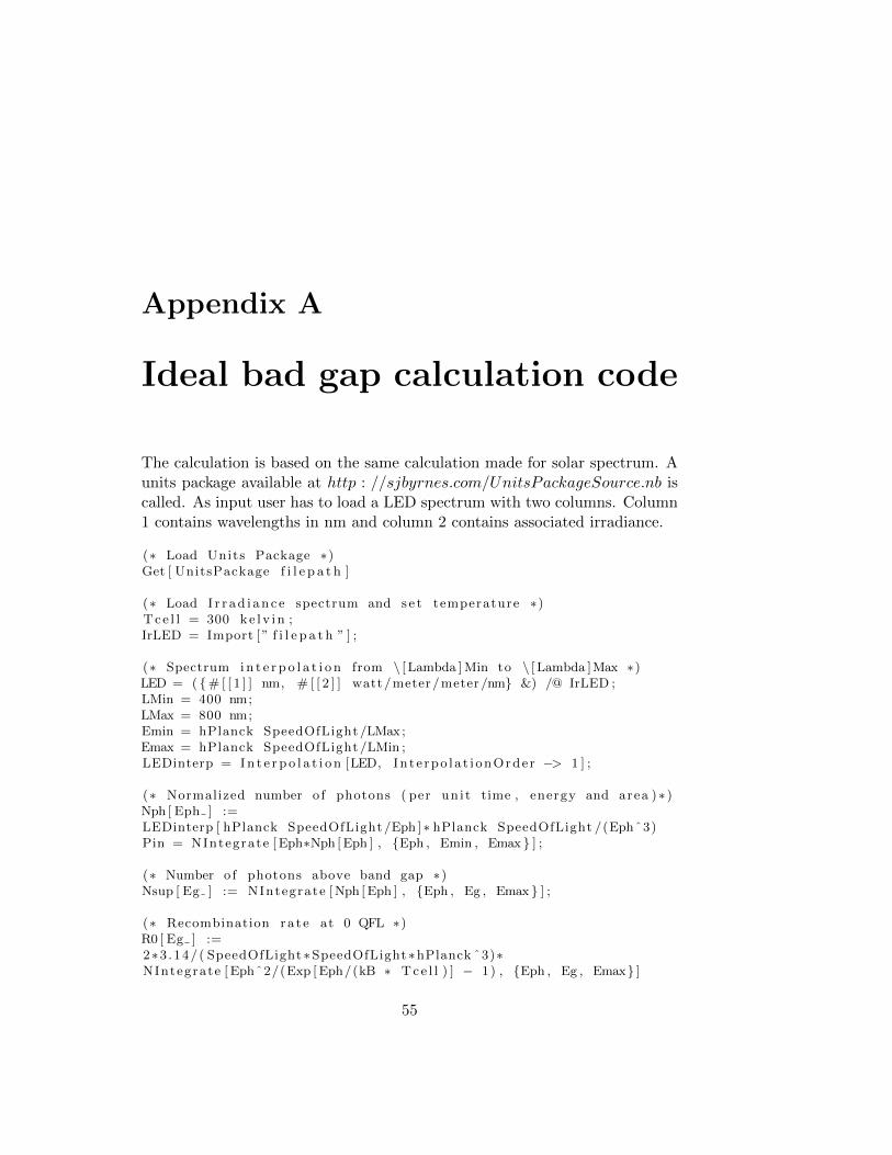
The calculation is based on the same calculation made for solar spectrum. Aunits package available at http : //sjbyrnes.com/UnitsPackageSource.nb iscalled. As input user has to load a LED spectrum with two columns. Column1 contains wavelengths in nm and column 2 contains associated irradiance.
(∗ Load Units Package ∗)Get [ UnitsPackage f i l e p a t h ]
(∗ Load I r r a d i a n c e spectrum and s e t temperature ∗)T ce l l = 300 k e l v i n ;IrLED = Import [ ” f i l e p a t h ” ] ;
(∗ Spectrum i n t e r p o l a t i o n from \ [ Lambda ] Min to \ [ Lambda ]Max ∗)LED = ( # [ [ 1 ] ] nm, # [ [ 2 ] ] watt/meter/meter/nm &) /@ IrLED ;LMin = 400 nm;LMax = 800 nm;Emin = hPlanck SpeedOfLight /LMax;Emax = hPlanck SpeedOfLight /LMin ;LEDinterp = I n t e r p o l a t i o n [LED, In t e rpo l a t i onOrde r −> 1 ] ;
(∗ Normalized number o f photons ( per un i t time , energy and area )∗ )Nph [ Eph ] :=LEDinterp [ hPlanck SpeedOfLight /Eph ]∗ hPlanck SpeedOfLight /(Ephˆ3)Pin = NIntegrate [ Eph∗Nph [ Eph ] , Eph , Emin , Emax ] ;
(∗ Number o f photons above band gap ∗)Nsup [ Eg ] := NIntegrate [ Nph [ Eph ] , Eph , Eg , Emax ] ;
(∗ Recombination ra t e at 0 QFL ∗)R0 [ Eg ] :=2∗3 .14/( SpeedOfLight∗SpeedOfLight∗hPlanck ˆ3)∗NIntegrate [ Ephˆ2/(Exp [ Eph/(kB ∗ T ce l l ) ] − 1) , Eph , Eg , Emax ]
55

56 APPENDIX A. IDEAL BAD GAP CALCULATION CODE
(∗ Current Density ∗)J [ V , Eg ] := e ∗(Nsup [ Eg ] − R0 [ Eg ]∗Exp [ e∗V/(kB ∗T ce l l ) ] )Jsc [ Eg ] := J [ 0 , Eg ] ;Voc [ Eg ] := kB Tc e l l /e ∗Log [ Nsup [ Eg ] /R0 [ Eg ] ] ;
PoutMax [ Eg ] := FindMaximum [ (V∗J [V, Eg ] ) , V, 0 ] [ [ 1 ] ]VAtMPP[ Eg ] := V / . FindMaximum [V∗J [V, Eg ] , V, 0 ] [ [ 2 ] ]JAtMPP[ Eg ] := J [VAtMPP[ Eg ] , Eg ] ;EtaMax [ Eg ] := PoutMax [ Eg ] / Pin ;
IBGcurve =Table [Eg/ eV , EtaMax [ Eg ] , Eg , 1 .1 eV , 3 eV , 0 .05 eV ] ;

Appendix B
Abeles calculation
Method
Recalling the Fresnel coefficients in both S and P polarization:
• S polarization
rk =nkqk − ˜nk+1 ˜qk+1
nkqk + ˜nk+1 ˜qk+1
tk =2nkqk
nkqk + ˜nk+1 ˜qk+1
• P polarization
rk =˜nk+1qk − nk ˜qk+1
˜nk+1qk + nk ˜qk+1
tk =2nkqk
˜nk+1qk + nk ˜qk+1
|<d1>|<d2>| |<di>|<di+1>| || | | | | | |
\ | | | | | | |\ | | | | | | |
theta , lambda \ | | | | | | |−−−−−−−−−−−−−−−−−−−−−−| | | | | | |
| | | | | | |n in | n1 | n2 | . . . | ni | ni+1 | . . . | n out
| | | | | | || | | | | | |
−−−−−−−−−−−−−−−−−−−−−−−−−−−−−−−−−−−−−−−−−−−−−−−−−−−−−−−−−−−−−−−−−−−−−−−−−−> z
57
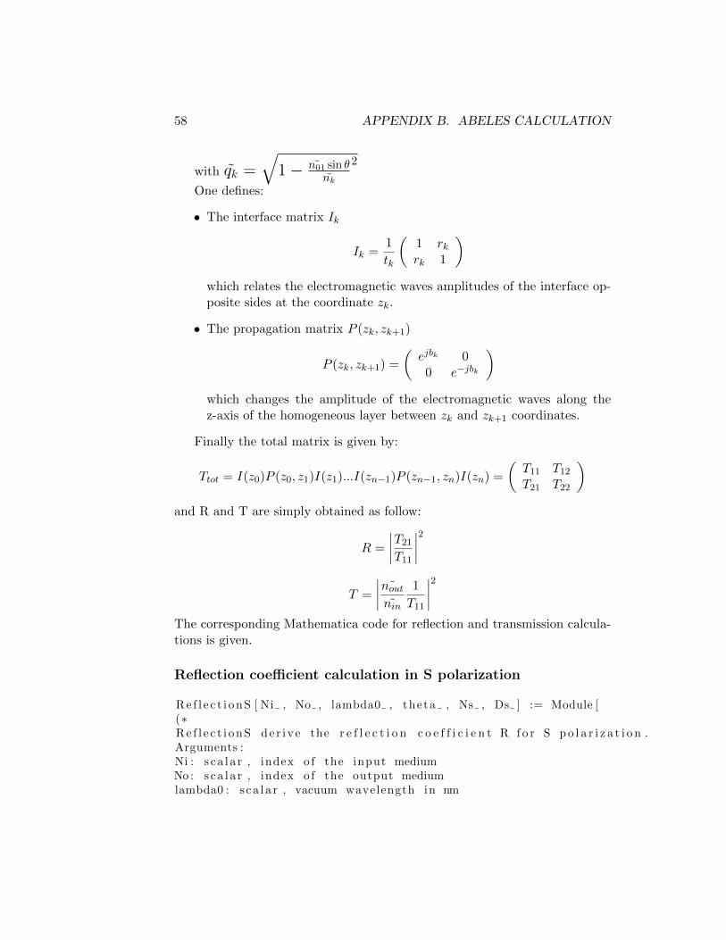
58 APPENDIX B. ABELES CALCULATION
with qk =√1− n01 sin θ
nk
2
One defines:
• The interface matrix Ik
Ik =1
tk
(1 rkrk 1
)which relates the electromagnetic waves amplitudes of the interface op-posite sides at the coordinate zk.
• The propagation matrix P (zk, zk+1)
P (zk, zk+1) =
(ejbk 0
0 e−jbk
)which changes the amplitude of the electromagnetic waves along thez-axis of the homogeneous layer between zk and zk+1 coordinates.
Finally the total matrix is given by:
Ttot = I(z0)P (z0, z1)I(z1)...I(zn−1)P (zn−1, zn)I(zn) =
(T11 T12T21 T22
)and R and T are simply obtained as follow:
R =
∣∣∣∣T21T11
∣∣∣∣2
T =
∣∣∣∣ ˜noutnin
1
T11
∣∣∣∣2The corresponding Mathematica code for reflection and transmission calcula-tions is given.
Reflection coefficient calculation in S polarization
R e f l e c t i o n S [ Ni , No , lambda0 , theta , Ns , Ds ] := Module [(∗R e f l e c t i o n S de r i v e the r e f l e c t i o n c o e f f i c i e n t R f o r S p o l a r i z a t i o n .Arguments :Ni : s ca l a r , index o f the input mediumNo : s ca l a r , index o f the output mediumlambda0 : s ca l a r , vacuum wavelength in nm

59
theta : s c a l a r , i n c i d e n c e ang le o f the wavevector in radNs : r e a l vector , conta in ing the o p t i c a l i n d i c e s o f each l a y e rDs : r e a l vector , conta in ing the l a y e r s depth in m∗) lambda , n , fq , fb , f r , f t , Pkk1 , Ik , M, r , R ,lambda = lambda0 ∗10ˆ(−9);n = Length [ Ds ] ;fq [ n ] := (1 − ( Ni∗Sin [ theta ] / n ) ˆ 2 ) ˆ 0 . 5 ;fb [ n , d ] := 2∗Pi/lambda∗d∗n∗ fq [ n ] ;f r [ n , n1 ] := (n∗ fq [ n ] − n1∗ fq [ n1 ] ) / ( n∗ fq [ n ] + n1∗ fq [ n1 ] ) ;f t [ n , n1 ] := (2∗n∗ fq [ n ] ) / ( n∗ fq [ n ] + n1∗ fq [ n1 ] ) ;Pkk1 = ConstantArray [ 0 , 2 , 2 ] ;Ik = ConstantArray [ 0 , 2 , 2 ] ;M = Ident i tyMatr ix [ 2 ] ;
(∗ I n t e r f a c e matrix I01 from the input r eg i on (0 ) to the f i r s t \l a y e r (1 ) ∗)
Ik = 1/ f t [ Ni , Ns [ [ 1 ] ] ] ∗ ( Ident i tyMatr ix [ 2 ] ) ;Ik [ [ 2 , 1 ] ] = f r [ Ni , Ns [ [ 1 ] ] ] / f t [ Ni , Ns [ [ 1 ] ] ] ;Ik [ [ 1 , 2 ] ] = Ik [ [ 2 , 1 ] ] ;M = Ik ;
I f [ n > 1 , (∗ I f the re i s more than 1 l a y e r ∗)For [ i = 1 , i <= n − 1 , i ++,
(∗ D e f i n i t i o n o f the propagat ion matrix P( zk , zk+1) along the z−a x i s in the homogenous l a y e r between zk and zk+1 coo rd ina t e s ∗)Pkk1 [ [ 1 , 1 ] ] = Exp [ I ∗ fb [ Ns [ [ i ] ] , Ds [ [ i ] ] ] ] ;Pkk1 [ [ 2 , 2 ] ] = Exp[− I ∗ fb [ Ns [ [ i ] ] , Ds [ [ i ] ] ] ] ;(∗ D e f i n i t i o n o f the i n t e r f a c e matrix I ( zk ) which r e l a t e s the \
ampl itudes o f e l e c t r omagne t i c waves o f the oppos i t e s i d e s o f the \i n t e r f a c e at the coord inate zk ∗)
Ik = 1/ f t [ Ns [ [ i ] ] , Ns [ [ i + 1 ] ] ] ∗ ( Ident i tyMatr ix [ 2 ] ) ;Ik [ [ 2 , 1 ] ] = f r [ Ns [ [ i ] ] , Ns [ [ i + 1 ] ] ] / f t [ Ns [ [ i ] ] , Ns [ [ i + 1 ] ] ] ;Ik [ [ 1 , 2 ] ] = Ik [ [ 2 , 1 ] ] ;(∗ Trans f e r t matrix M ∗)M = M. Pkk1 . Ik ;
]] ;
(∗ Propagation matrix P(n−1,n) in the l a s t l a y e r ∗)Pkk1 [ [ 1 , 1 ] ] = Exp [ I ∗ fb [ Ns [ [ n ] ] , Ds [ [ n ] ] ] ] ;Pkk1 [ [ 2 , 2 ] ] = Exp[− I ∗ fb [ Ns [ [ n ] ] , Ds [ [ n ] ] ] ] ;
(∗ I n t e r f a c e matrix I (n , out ) toward the output r eg i on ∗)Ik = 1/ f t [ Ns [ [ n ] ] , No ] ∗ ( Ident i tyMatr ix [ 2 ] ) ;
60 APPENDIX B. ABELES CALCULATION
Ik [ [ 2 , 1 ] ] = f r [ Ns [ [ n ] ] , No ] / f t [ Ns [ [ n ] ] , No ] ;Ik [ [ 1 , 2 ] ] = Ik [ [ 2 , 1 ] ] ;
(∗ Total t r a n s f e r matrix M ∗)M = M. Pkk1 . Ik ;
(∗ Total r e f l e c t i o n c o e f f i c i e n t ∗)r = M[ [ 2 , 1 ] ] /M[ [ 1 , 1 ] ] ;
R = (Abs [ r ] ) ˆ 2 ;
Return [R]]
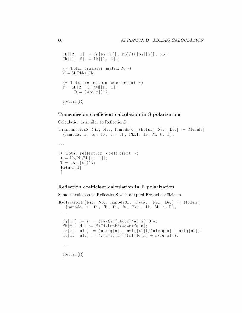
Transmission coefficient calculation in S polarization
Calculation is similar to ReflectionS.
TransmissionS [ Ni , No , lambda0 , theta , Ns , Ds ] := Module [ lambda , n , fq , fb , f r , f t , Pkk1 , Ik , M, t , T ,
. . .
(∗ Total r e f l e c t i o n c o e f f i c i e n t ∗)t = No/Ni/M[ [ 1 , 1 ] ] ;T = (Abs [ t ] ) ˆ 2 ;Return [T]]
Reflection coefficient calculation in P polarization
Same calculation as ReflectionS with adapted Fresnel coefficients.
Ref l e c t i onP [ Ni , No , lambda0 , theta , Ns , Ds ] := Module [ lambda , n , fq , fb , f r , f t , Pkk1 , Ik , M, r , R ,
. . .
fq [ n ] := (1 − ( Ni∗Sin [ theta ] / n ) ˆ 2 ) ˆ 0 . 5 ;fb [ n , d ] := 2∗Pi/lambda∗d∗n∗ fq [ n ] ;f r [ n , n1 ] := ( n1∗ fq [ n ] − n∗ fq [ n1 ] ) / ( n1∗ fq [ n ] + n∗ fq [ n1 ] ) ;f t [ n , n1 ] := (2∗n∗ fq [ n ] ) / ( n1∗ fq [ n ] + n∗ fq [ n1 ] ) ;
. . .
Return [R]]

61
Transmission coefficient calculation in P polarization
Calculation is similar to ReflectionP.
TransmissionS [ Ni , No , lambda0 , theta , Ns , Ds ] := Module [ lambda , n , fq , fb , f r , f t , Pkk1 , Ik , M, t , T ,
. . .
(∗ Total r e f l e c t i o n c o e f f i c i e n t ∗)t = No/Ni/M[ [ 1 , 1 ] ] ;T = (Abs [ t ] ) ˆ 2 ;Return [T]]
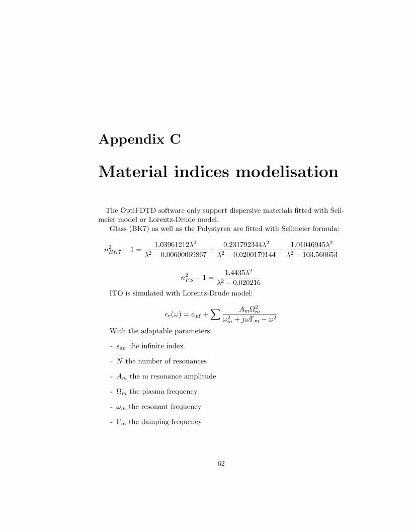
Appendix C
Material indices modelisation
The OptiFDTD software only support dispersive materials fitted with Sell-meier model or Lorentz-Drude model.
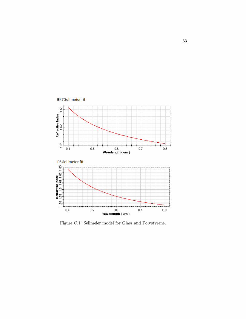
Glass (BK7) as well as the Polystyren are fitted with Sellmeier formula:
n2BK7 − 1 =1.03961212λ2
λ2 − 0.00600069867+
0.231792344λ2
λ2 − 0.0200179144+
1.01046945λ2
λ2 − 103.560653
n2PS − 1 =1.4435λ2
λ2 − 0.020216
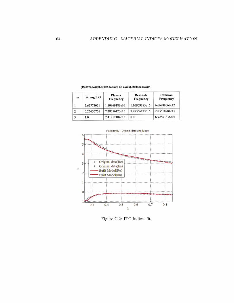
ITO is simulated with Lorentz-Drude model:
εr(ω) = εinf +∑ AmΩ2
m
ω2m + jωΓm − ω2
With the adaptable parameters:
- εinf the infinite index
- N the number of resonances
- Am the m resonance amplitude
- Ωm the plasma frequency
- ωm the resonant frequency
- Γm the damping frequency
62
63
Figure C.1: Sellmeier model for Glass and Polystyrene.
64 APPENDIX C. MATERIAL INDICES MODELISATION
Figure C.2: ITO indices fit.