Indium gallium nitride multijunction solar cell …Calhoun: The NPS Institutional Archive Theses and...
114
Calhoun: The NPS Institutional Archive Theses and Dissertations Thesis Collection 2007-06 Indium gallium nitride multijunction solar cell simulation using silvaco atlas Garcia, Baldomero Monterey California. Naval Postgraduate School http://hdl.handle.net/10945/3423
Transcript of Indium gallium nitride multijunction solar cell …Calhoun: The NPS Institutional Archive Theses and...

Calhoun: The NPS Institutional Archive
Theses and Dissertations Thesis Collection
2007-06
Indium gallium nitride multijunction solar cell
simulation using silvaco atlas
Garcia, Baldomero
Monterey California. Naval Postgraduate School
http://hdl.handle.net/10945/3423

NAVAL
POSTGRADUATE SCHOOL
MONTEREY, CALIFORNIA
THESIS
Approved for public release; distribution is unlimited
INDIUM GALLIUM NITRIDE MULTIJUNCTION SOLAR CELL SIMULATION USING SILVACO ATLAS
by
Baldomero Garcia, Jr.
June 2007
Thesis Advisor: Sherif Michael Second Reader: Todd Weatherford

THIS PAGE INTENTIONALLY LEFT BLANK

i
REPORT DOCUMENTATION PAGE Form Approved OMB No. 0704-0188Public reporting burden for this collection of information is estimated to average 1 hour per response, including the time for reviewing instruction, searching existing data sources, gathering and maintaining the data needed, and completing and reviewing the collection of information. Send comments regarding this burden estimate or any other aspect of this collection of information, including suggestions for reducing this burden, to Washington headquarters Services, Directorate for Information Operations and Reports, 1215 Jefferson Davis Highway, Suite 1204, Arlington, VA 22202-4302, and to the Office of Management and Budget, Paperwork Reduction Project (0704-0188) Washington DC 20503. 1. AGENCY USE ONLY (Leave blank)
2. REPORT DATE June 2007
3. REPORT TYPE AND DATES COVERED Master’s Thesis
4. TITLE AND SUBTITLE Indium Gallium Nitride Multijunction Solar Cell Simulation Using Silvaco Atlas 6. AUTHOR(S) Baldomero Garcia, Jr.
5. FUNDING NUMBERS
7. PERFORMING ORGANIZATION NAME(S) AND ADDRESS(ES) Naval Postgraduate School Monterey, CA 93943-5000
8. PERFORMING ORGANIZATION REPORT NUMBER
9. SPONSORING /MONITORING AGENCY NAME(S) AND ADDRESS(ES)
N/A
10. SPONSORING/MONITORING AGENCY REPORT NUMBER
11. SUPPLEMENTARY NOTES The views expressed in this thesis are those of the author and do not reflect the official policy or position of the Department of Defense or the U.S. Government. 12a. DISTRIBUTION / AVAILABILITY STATEMENT Approved for public release; distribution is unlimited
12b. DISTRIBUTION CODE
13. ABSTRACT (maximum 200 words) This thesis investigates the potential use of wurtzite Indium Gallium Nitride as
photovoltaic material. Silvaco Atlas was used to simulate a quad-junction solar cell. Each of the junctions was made up of Indium Gallium Nitride. The band gap of each junction was dependent on the composition percentage of Indium Nitride and GalliumNitride within Indium Gallium Nitride. The findings of this research show that Indium Gallium Nitride is a promising semiconductor for solar cell use.
15. NUMBER OF PAGES
113
14. SUBJECT TERMS Solar cell, photovoltaic device, Indium Gallium Nitride, Silvaco Atlas.
16. PRICE CODE
17. SECURITY CLASSIFICATION OF REPORT
Unclassified
18. SECURITY CLASSIFICATION OF THIS PAGE
Unclassified
19. SECURITY CLASSIFICATION OF ABSTRACT
Unclassified
20. LIMITATION OF ABSTRACT
UL NSN 7540-01-280-5500 Standard Form 298 (Rev. 2-89) Prescribed by ANSI Std. 239-18

ii
THIS PAGE INTENTIONALLY LEFT BLANK

iii
Approved for public release; distribution is unlimited
INDIUM GALLIUM NITRIDE MULTIJUNCTION SOLAR CELL SIMULATION USING SILVACO ATLAS
Baldomero Garcia, Jr. Lieutenant Commander, United States Navy
B.S., U.S. Naval Academy, 1995
Submitted in partial fulfillment of the requirements for the degree of
MASTER OF SCIENCE IN ELECTRICAL ENGINEERING
from the
NAVAL POSTGRADUATE SCHOOL June 2007
Author: Baldomero Garcia, Jr.
Approved by: Sherif Michael Thesis Advisor
Todd Weatherford Second Reader
Jeffrey B. Knorr Chairman, Department of Electrical and Computer Engineering

iv
THIS PAGE INTENTIONALLY LEFT BLANK

v
ABSTRACT
This thesis investigates the potential use of wurtzite
Indium Gallium Nitride as photovoltaic material. Silvaco
Atlas was used to simulate a quad-junction solar cell. Each
of the junctions was made up of Indium Gallium Nitride. The
band gap of each junction was dependent on the composition
percentage of Indium Nitride and Gallium Nitride within
Indium Gallium Nitride. The findings of this research show
that Indium Gallium Nitride is a promising semiconductor for
solar cell use.

vi
THIS PAGE INTENTIONALLY LEFT BLANK

vii
TABLE OF CONTENTS
I. INTRODUCTION ............................................1 A. BACKGROUND .........................................1 B. OBJECTIVE ..........................................1 C. RELATED WORK .......................................1 D. ORGANIZATION .......................................2
1. Purpose of Solar Cells ........................2 2. Simulation Software ...........................2 3. Indium Gallium Nitride ........................3 4. Simulation ....................................3
II. SOLAR CELL AND SEMICONDUCTOR BASICS .....................5 A. SEMICONDUCTOR FUNDAMENTALS .........................5
1. Classification of Materials ...................5 2. Atomic Structure ..............................7 3. Electrons and Holes ...........................9 4. Direct and Indirect Band Gaps ................12 5. Fermi Level ..................................13
B. SOLAR CELL FUNDAMENTALS ...........................14 1. History of Solar Cells .......................14 2. The Photovoltaic Effect ......................15
a. The Electromagnetic Spectrum ............17 b. Band Gap ................................18 c. Solar Cell Junctions ....................19 d. Lattice Matching ........................20 e. AM0 Spectrum ............................22 f. Current-Voltage Curves ..................24 g. Electrical Output .......................25
C. CHAPTER CONCLUSIONS ...............................26 III. SILVACO ATLAS SIMULATION SOFTWARE ......................27
A. VIRTUAL WAFER FAB .................................27 B. SILVACO ATLAS .....................................28 C. INPUT FILE STRUCTURE ..............................29
1. Structure Specification ......................31 a. Mesh ....................................31 b. Region ..................................32 c. Electrodes ..............................34 d. Doping ..................................35
2. Materials Model Specification ................35 a. Material ................................36 b. Models ..................................36 c. Contact .................................37 d. Interface ...............................37

viii
3. Numerical Method Selection ...................38 4. Solution Specification .......................39
a. Log .....................................39 b. Solve ...................................40 c. Load and Save ...........................40
5. Results Analysis .............................41 D. CONCLUSION ........................................42
IV. INDIUM GALLIUM NITRIDE .................................43 A. A FULL SPECTRUM PHOTOVOLTAIC MATERIAL .............43 B. RADIATION-HARD SEMICONDUCTOR MATERIAL .............47 C. INDIUM GALLIUM NITRIDE CHALLENGES .................48
V. SIMULATION OF INDIUM GALLIUM NITRIDE IN SILVACO ATLAS ..49 A. SINGLE-JUNCTION SOLAR CELL ........................50 B. DUAL-JUNCTION SOLAR CELL ..........................52 C. THREE-JUNCTION SOLAR CELL .........................54 D. QUAD-JUNCTION SOLAR CELL ..........................57
VI. CONCLUSIONS AND RECOMMENDATIONS ........................67 A. RESULTS AND CONCLUSIONS ...........................67 B. RECOMMENDATIONS FOR FUTURE RESEARCH ...............67
APPENDIX A: SILVACO ATLAS INPUT DECK ........................69 A. TOP JUNCTION: IN0.20GA0.80N, EG=2.66 EV..............69 B. SECOND JUNCTION: IN0.57GA0.43N, EG=1.6 EV............73 C. THIRD JUNCTION: IN0.68GA0.32N, EG=1.31 EV............77 D. BOTTOM JUNCTION: IN0.78GA0.22N, EG=1.11 EV...........80
APPENDIX B: MATLAB CODE .....................................85 A. INDIUM GALLIUM NITRIDE BAND GAP CALCULATIONS ......85 B. CONVERSION FROM DIELECTRIC CONSTANTS (EPSILONS) TO
REFRACTION COEFFICIENTS (N, K) ....................86 C. CONVERSION FROM PHOTON ENERGY (EV) TO WAVELENGTH
(UM) ..............................................86 D. IV CURVE PLOTS FOR INDIUM GALLIUM NITRIDE QUAD
JUNCTION SOLAR CELL ...............................87 E. AIR MASS ZERO PLOTS ...............................90
LIST OF REFERENCES ..........................................91 INITIAL DISTRIBUTION LIST ...................................95

ix
LIST OF FIGURES
Figure 1. Materials classified by conductivity (From [6]).............................................5
Figure 2. Partial periodic table (After [7])...............6 Figure 3. Silicon atomic structure (From [8])..............7 Figure 4. Silicon atom covalent bonds (From [1, p. 11])....8 Figure 5. Band gap diagrams (From [1, p. 8])...............9 Figure 6. Doping: n-type and p-type (From [1, p. 13]).....10 Figure 7. Direct and indirect band gaps (After [1, p.
24])............................................12 Figure 8. Fermi level: intrinsic case (After [9, p. 42])..14 Figure 9. Fermi level: n-type case (After [9, p. 42]).....14 Figure 10. Fermi level: p-type case (After [9, p. 42]).....14 Figure 11. The electromagnetic spectrum (From [13])........17 Figure 12. Effect of light energy on different band gaps
(From [15]).....................................19 Figure 13. Simple cubic lattice structure (From [16])......20 Figure 14. Lattice constants (From [17])...................21 Figure 15. Lattice constant for InN and GaN (From [18])....22 Figure 16. AM0 spectrum (Wavelength vs Irradiance) (After
[19])...........................................23 Figure 17. AM0 spectrum (Energy vs Irradiance) (After
[19])...........................................24 Figure 18. Sample IV curve used in efficiency calculations
(After [20])....................................24 Figure 19. Solar cell IV characteristic (From [21])........26 Figure 20. Silvaco’s Virtual Wafer Fabrication Environment
(From [22]).....................................27 Figure 21. Atlas inputs and outputs (From [23, p. 2-2])....28 Figure 22. Atlas command groups and primary statements
(From [23, p. 2-8]).............................30 Figure 23. Atlas mesh (From 2, p.18])......................31 Figure 24. Atlas region (From [2, p. 19])..................33 Figure 25. Atlas regions with materials defined (From [2,
p. 19]).........................................33 Figure 26. Atlas electrodes (From [2, p. 20])..............34 Figure 27. Atlas doping (From [2, p. 21])..................35 Figure 28. Atlas material models specification (After [23,
p. 2-8])........................................36 Figure 29. Atlas numerical method selection (After [23, p.
2-8])...........................................38 Figure 30. Atlas solution specification (After [23, p. 2-
8]).............................................39 Figure 31. Atlas results analysis (After [23, p. 2-8]).....41

x
Figure 32. Sample TonyPlot IV curve........................42 Figure 33. InGaN band gap as a function of In composition
(After [25])....................................43 Figure 34. InGaN band gap and solar spectrum comparison
(After [26])....................................44 Figure 35. Evidence of 0.7 eV band gap for indium nitride
(From [29]).....................................46 Figure 36. InGaN band gap as a function of In
concentration...................................47 Figure 37. Simple single-junction InGaN solar cell.........50 Figure 38. Four single-junction IV curves..................51 Figure 39. Simple dual-junction InGaN solar cell...........52 Figure 40. Dual-junction InGaN solar cell IV curve.........53 Figure 41. Simple three-junction InGaN solar cell..........55 Figure 42. Three-junction InGaN solar cell IV curve........56 Figure 43. Simple quad-junction InGaN solar cell...........58 Figure 44. Quad-junction InGaN solar cell IV curve.........59 Figure 45. Spectrolab’s solar cell efficiencies (From
[34])...........................................60 Figure 46. Comparison of InGaN band gap formulas...........62 Figure 47. IV curve for In0.20Ga0.80N using different band
gaps............................................63 Figure 48. Quad-junction InGaN solar cell IV curve using
calculated band gaps from [37] formula..........64
xi
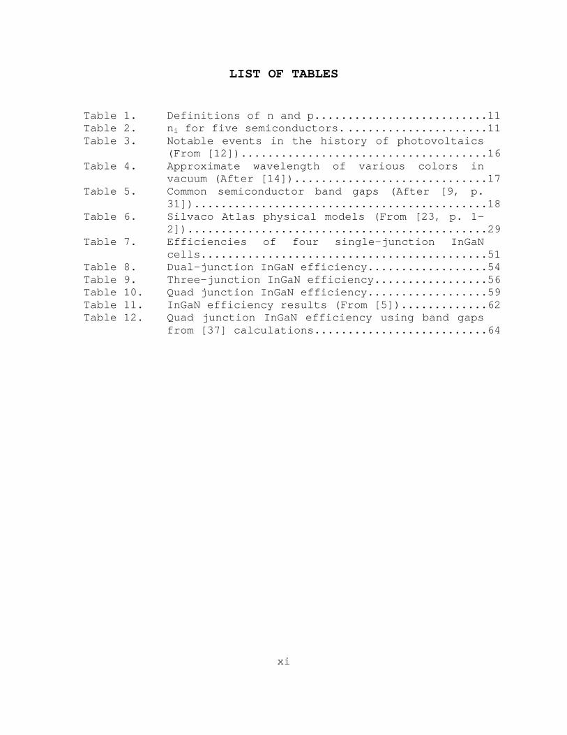
LIST OF TABLES
Table 1. Definitions of n and p..........................11 Table 2. ni for five semiconductors. .....................11 Table 3. Notable events in the history of photovoltaics
(From [12]).....................................16 Table 4. Approximate wavelength of various colors in
vacuum (After [14]).............................17 Table 5. Common semiconductor band gaps (After [9, p.
31])............................................18 Table 6. Silvaco Atlas physical models (From [23, p. 1-
2]).............................................29 Table 7. Efficiencies of four single-junction InGaN
cells...........................................51 Table 8. Dual-junction InGaN efficiency..................54 Table 9. Three-junction InGaN efficiency.................56 Table 10. Quad junction InGaN efficiency..................59 Table 11. InGaN efficiency results (From [5]).............62 Table 12. Quad junction InGaN efficiency using band gaps
from [37] calculations..........................64

xii
THIS PAGE INTENTIONALLY LEFT BLANK

xiii
ACKNOWLEDGMENTS
First, I would like to thank Professor Sherif Michael
for his help and guidance during the research process. His
insight was invaluable when faced with difficult problems.
Second, I would like to thank Professor Todd
Weatherford for clarifying issues regarding the use of
Silvaco Atlas. He was also critical in finding points of
contact at Lawrence Berkeley Laboratory.
Third, I would like to thank Dr. Wladek Walukiewicz
from the Material Sciences Division at Lawrence Berkeley
National Laboratory. He and his team are the world-wide
leaders in Indium Gallium Nitride material science research.
Their research was my inspiration to start this research
project.
Fourth, I would like to thank Dr. Petra Specht from
Lawrence Berkeley National Laboratory. She provided key data
used in this research.
And last, but not least, I would like to thank my wife,
Nozomi and our children, Oscar and Yuuki, for their patience
and support during my time at the Naval Postgraduate School.

xiv
THIS PAGE INTENTIONALLY LEFT BLANK

xv
EXECUTIVE SUMMARY
One of the primary goals of solar cell design is to
improve efficiency. Indium Gallium Nitride is a material
that has undergone extensive research since 2002 as a
potential photovoltaic material. By varying the composition
of Indium Nitride and Gallium Nitride within Indium Gallium
Nitride, the band gap of this semiconductor material can be
changed. The band gap range of Indium Gallium Nitride
matches closely the visible solar spectrum frequencies.
Hence, a high-efficiency solar cell can be potentially
developed by having several Indium Gallium Nitride
junctions.
The use of Silvaco Atlas as a simulation tool can aid
in identifying whether Indium Gallium Nitride can be used
for photovoltaics. Previous research at the Naval
Postgraduate School has demonstrated the viability of
Silvaco Atlas as a solar cell modeling mechanism.
Finding high-efficiency solar cell models is of great
interest in space applications. By increasing the efficiency
of photovoltaics, the number of solar panels is decreased.
Therefore, the overall weight that needs to be launched into
space is reduced. A cost-reduction can be achieved over the
life of the space power system.
Research at Lawrence Berkeley National Laboratory
(LBNL) has been ongoing since 2002 in trying to develop
high-efficiency solar cells. One of the materials LBNL has
been investigating is Indium Gallium Nitride. In addition to
the band gap range, Indium Gallium Nitride also has other
characteristics that are beneficial for space applications.

xvi
The radiation level that Indium Gallium Nitride is able to
withstand is approximately two orders of magnitude greater
than current multijunction solar cell materials. Therefore,
it is of great interest to continue to research Indium
Gallium Nitride and its possibilities as photovoltaic
material.
The goal of this research was to investigate the
efficiency of Indium Gallium Nitride solar cells using the
Silvaco Atlas TCAD simulation software. No other TCAD
simulations have been performed on InGaN solar cells. The
methodology of this research progressed from single to
multi-junction cells. The simulation results predicted
efficiencies as high as 41% for a four-junction solar cell.
Further refinements of the simulation model are still
possible. Actual production of a single-junction solar cell
is the next step required to eventually manufacture high-
efficiency, multi-junction InGaN solar cells.

1
I. INTRODUCTION
A. BACKGROUND
One of the most important problems to solve in space
solar cell design is efficiency. As efficiency increases,
the required number of cells decreases to fulfill electrical
power requirements.
Solar cell efficiencies have improved over time by
increasing the number of junctions. Each junction is capable
of extracting energy from a portion of the solar spectrum.
A new path to improving efficiency is to use new
photovoltaic materials such as wurtzite Indium Gallium
Nitride. Indium Gallium Nitride possesses a band gap range
that can extract energy from a large portion of the visible
solar spectrum.
B. OBJECTIVE
The objective of this thesis is to simulate Indium
Gallium Nitride solar cells to predict their efficiencies.
After obtaining the efficiencies, a comparison is made with
current solar cell efficiencies. Silvaco Atlas TCAD
simulation software is used to investigate these
efficiencies.
C. RELATED WORK
Previous Silvaco Atlas solar cell simulations have been
performed by Naval Postgraduate School researchers.
Michalopoulos [1] investigated the feasibility of designing
solar cells using Silvaco Atlas. To demonstrate the use of

2
Silvaco Atlas, Michalopoulos simulated single-junction solar
cells with Gallium Arsenide, dual-junction solar cells with
Indium Gallium Phosphide and Gallium Arsenide, and triple-
junction cells with Indium Gallium Phosphide, Gallium
Arsenide, and Germanium. The highest efficiency obtained
with the triple-junction was 29.5%. This result matched the
29.3% efficiency obtained with actual triple-junction solar
cells in production. Bates [2] provided excellent background
on the use of Silvaco Atlas. Green [3] and Canfield [4]
continued to work on Silvaco Atlas solar cell design. Matlab
functions and Silvaco Atlas code were modified from [1]-[4]
to perform simulations in this research.
A previous Indium Gallium Nitride simulation has been
performed [5] using fundamental semiconductor physics
formulas. The results of this research are compared with
those of [5].
D. ORGANIZATION
1. Purpose of Solar Cells
The purpose of solar cells is to convert light energy
into electrical energy. Light is made up of photons. Photons
carry energy that is dependent on the color, or wavelength
of light. Electrical energy is generated when photons excite
electrons from the valence band into the conduction band in
semiconductor materials. Chapter II covers fundamental
concepts of solar cells and semiconductor materials.
2. Simulation Software
Silvaco Atlas was used as the simulation software in
this thesis. Silvaco offers a suite of software programs

3
that can act as a Virtual Wafer Fabrication (VWF) tool. The
Naval Postgraduate School has had multiple researchers
publish theses on the use of Silvaco Atlas for the purpose
of solar cell modeling. Chapter III covers the basics of
Silvaco Atlas.
3. Indium Gallium Nitride
Wurtzite Indium Gallium Nitride (InGaN) is a
semiconductor that has the potential to produce high-
efficiency solar cells. Dr. Wladek Walukiewicz, of Lawrence
Berkeley National Laboratory (Solar Energy Materials
Research Group), has been conducting extensive InGaN
research for the purposes of producing photovoltaic
material. Chapter IV covers the characteristics of InGaN,
its potential, its material science research status, and its
current limitations.
4. Simulation
Based on the optical characteristics of InGaN,
simulations were performed using Silvaco Atlas. Chapter V
covers the findings of the simulations. Chapter VI covers
the conclusions and recommendations. Finally, the appendices
include the code used in Silvaco Atlas as well as Matlab.

4
THIS PAGE LEFT INTENTIONALLY BLANK

5
II. SOLAR CELL AND SEMICONDUCTOR BASICS
This thesis examines a novel process to simulate Indium
Gallium Nitride solar cells. Before delving into the
simulation, this chapter covers the fundamental principles
of solar cells and semiconductors. The properties of the
semiconductor material determine the characteristics of the
photovoltaic device.
A. SEMICONDUCTOR FUNDAMENTALS
1. Classification of Materials
Materials can be categorized according to their
electrical properties as conductors, insulators or
semiconductors. The conductivity σ is a key parameter in
identifying the type of material.
Figure 1 presents a sample of materials based on
conductivity. The semiconductors fall between the insulators
and the conductors.
Figure 1. Materials classified by conductivity (From [6]).

6
Semiconductors can be found in elemental or compound
form. Silicon (Si) and Germanium (Ge) are examples of
elemental semiconductors. Both of these semiconductors
belong to group IV of the periodic table.
Figure 2 shows an abbreviated periodic table. In
addition to the group IV semiconductors, compounds can be
made with elements from groups III and V, respectively.
Examples of III-V semiconductors include Aluminum Phosphide
(AlP), Gallium Nitride (GaN), Indium Phosphide (InP),
Gallium Arsenide (GaAs), among others. It is also possible
to make semiconductor compounds from groups II-VI, such as
Zinc Oxide (ZnO), Cadmium Telluride (CdTe), Mercury Sulfide
(HgS), among others. The subject of this thesis is the
ternary alloy wurtzite Indium Gallium Nitride (InGaN).
Indium and Gallium are group III elements, while Nitrogen is
a group V element.
Figure 2. Partial periodic table (After [7]).

7
2. Atomic Structure
Since Silicon is the most commonly used semiconductor
in solar cells today, a brief analysis of this element is
presented.
Silicon has 14 protons and 14 neutrons in its nucleus.
The 14 electrons are distributed in three shells.
Figure 3 shows the arrangement of electrons in a
Silicon atom. There are two electrons in the first shell,
eight electrons in the second shell and four electrons in
the outer shell. When Silicon atoms are together, the atoms
from the outer shells form covalent bonds. Hence, a Silicon
atom forms bonds with four other Silicon atoms.
Figure 3. Silicon atomic structure (From [8]).
As shown in Figure 4, the covalent bonds formed by the
silicon atoms are represented by the elliptical dotted
lines. In the absence of an electron, the covalent bond
ceases to exist. A hole takes the place of the electron.

8
Figure 4. Silicon atom covalent bonds (From [1, p. 11]).
Energy bands are a fundamental concept of semiconductor
physics. These energy bands are the valence band, the
conduction band, and the forbidden gap or band gap [9, p.
27]. When an electron is in the valence band, the covalent
bond exists. In order for the electron to move from the
valence band into the conduction band, energy is required to
excite the electron. The band gap energy is the minimum
energy required for the electron to make the move from the
valence band into the conduction band.
Figure 5 shows the band gap diagrams for conductors,
insulators, and semiconductors. This figure also reinforces
the differences among the three types of materials according
to their electric properties. In the case of conductors, the
band gap is small or non-existent. By contrast, insulators
have wide band gaps. Therefore, it takes much more energy
for the insulator to have electrons in the conduction band.

9
Figure 5. Band gap diagrams (From [1, p. 8]).
Semiconductors have band gaps that are dependent on the
material. Because band gap is also dependent on temperature,
it should be noted that all quoted band gaps in this thesis
are at room temperature (300 K.)
3. Electrons and Holes
A semiconductor at absolute zero temperature is unable
to conduct heat or electricity [10, p. 44]. All of the
semiconductor’s electrons are bonded. The electrons acquire
kinetic energy as the temperature is increased. Some of the
electrons are freed and move into the conduction band. These
electrons are able to conduct charge or energy. The areas
left by these electrons in the valence band are called
holes. As the temperature of the semiconductor increases,
the number of free electrons and holes increases as well.
Therefore, the conductivity of the semiconductor is directly
proportional to temperature increases.
The conductivity of the semiconductor can be altered by
exposing it to light or by doping it. Photoconductivity
consists of exposing the semiconductor with photon energy

10
larger than the semiconductor’s band gap. Doping consists of
adding impurities to the semiconductor material.
Figure 6 shows n-type and p-type doping. The atom of
the semiconductor is represented by the blue circle and a
+4. For example, a silicon atom has four electrons in its
outer shell. When silicon atoms are n-doped, atoms from
group V of the periodic table are added. Each added group V
atom provides an extra electron to donate. When silicon
atoms are p-doped, the atoms from group III of the periodic
table are added. Each group III atom has one less electron
than silicon. Therefore, a hole is added. Doping increases
the number of carriers in the semiconductor material.
Figure 6. Doping: n-type and p-type (From [1, p. 13]).
An intrinsic semiconductor is a pure semiconductor with
a negligible amount of impurity atoms [9, p.34]. By
definition, the number of electrons and holes in a
semiconductor are represented by n and p. See Table 1.

11
3
3
number of electronscm
number of holescm
n
p
=
=
Table 1. Definitions of n and p.
In the case of an intrinsic semiconductor, the
following case occurs:
in p n= =
For example purposes, ni is given for GaAs, Si and Ge
and room temperature [9, p.34]. Data for InN and GaN are
from [11]. See Table 2.
6
3
10
3
13
3
22
3
22
3
2 10
1 10
2 10
6.2 10
8.9 10
GaAsi
Sii
Gei
InNi
GaNi
ncm
ncm
ncm
ncm
ncm
×=
×=
×=
×=
×=
Table 2. ni for five semiconductors.
When solar cells utilize semiconductor materials from
Table 2, the current level is highest for Ge and lowest for
GaAs. The current levels correspond in rank to the ni levels
provided in Table 2. No data exists for InN or GaN current
levels as photovoltaic materials.

12
4. Direct and Indirect Band Gaps
Since the band gap is the minimum energy required to
move an electron from the valence band into the conduction
band, it is necessary to distinguish between direct and
indirect band gaps.
Figure 7 shows the concept of direct and indirect band
gaps. The blue portion represents the valence band. The tan
portion represents the conduction band.
Figure 7. Direct and indirect band gaps (After [1, p. 24]).
When the valence band and the conduction band coincide
in wave vector k, the semiconductor has a direct band gap.
When the valence band and the conduction band have different
wave vector k, the semiconductor has an indirect band gap.
The k vector represents a difference in momentum. Photons
have negligible momentum. In order to excite an electron
from the valence band to the conduction band in an indirect
band gap semiconductor, in addition to a photon, a phonon is
required. The phonon is a lattice vibration. The phonon

13
transfers its momentum to the electron at the time the
photon is absorbed. Therefore, a direct band gap
semiconductor is generally better for optoelectronics.
Silicon is an example of an indirect band gap semiconductor.
Gallium Arsenide and wurtzite Indium Gallium Nitride are
examples of direct band gap semiconductors.
5. Fermi Level
The Fermi function f(E) specifies how many of the
existing states at energy E are filled with an electron [9,
p.42]. The Fermi function is a probability distribution
function defined as follows:
( )1( )
1FE E
kT
f Ee
−=+
Where EF is the Fermi level, k is Boltzmann’s constant,
and T is the temperature in Kelvin.
From the Fermi function, it can be determined that when
E=EF, then f(E)=f(EF)=0.5.
Figure 8 shows the Fermi level for an intrinsic
semiconductor. Figure 9 shows the Fermi level for n-type
semiconductor. Figure 10 shows the Fermi level for p-type
semiconductor. From these Figures, it can be deduced that
the n-type material has a larger electron carrier
distribution and the p-type material has a larger hole
carrier distribution.

14
Figure 8. Fermi level: intrinsic case (After [9, p. 42]).
Figure 9. Fermi level: n-type case (After [9, p. 42]).
Figure 10. Fermi level: p-type case (After [9, p. 42]).
B. SOLAR CELL FUNDAMENTALS
After covering the basics of semiconductors, the
logical step is to continue with solar cell fundamentals.
1. History of Solar Cells
Solar cell research started when Edmund Bequerel
discovered the photovoltaic effect in 1839. He recorded that
an electric current was produced when light was applied to a
silver coated platinum electrode immersed in electrolyte.
The next significant step was performed by William Adams and
Richard Day in 1876. They discovered that a photocurrent
appeared when selenium was contacted by two heated platinum
contacts. However, current was produced spontaneously by the
action of light. Continuing to build on these efforts,
Charles Fritts developed the first large area solar cell in
1894. He pressed a layer of selenium between gold and
another metal. Progress continued as the theory of metal-
15
semiconductor barrier layers was established by Walter
Schottky and other. In the 1950s, silicon was used for solid
state electronics. Silicon p-n junctions were used to
improve on the performance of the Schottky barrier. These
silicon junctions had better rectifying action and
photovoltaic behavior. In 1954, Chapin, Fuller and Pearson
developed the first silicon solar cell, with a reported
efficiency of 6%. However, the cost per Watt associated with
these solar cells made them prohibitively expensive for
terrestrial use. However, locations where power generation
was not feasible (i.e., space) were suitable for solar
cells. Satellites were the first clear application for
silicon solar cells. Since that time, solar cells have
progressed steadily both in terms of efficiency as well as
materials used their production [10, p. 2].
Table 3 shows a brief list of events in the history of
photovoltaics from 1939 until 2002.
2. The Photovoltaic Effect
The photovoltaic effect is the process by which a solar
cell converts the energy from light into electrical energy.
Light is made up of photons. The energy of these photons
depends on the color (wavelength) of light. The material
that makes up the solar cell determines the photovoltaic
properties when light is applied [10, p. 1].
When light is absorbed by matter, such as metal,
photons provide the energy for electrons to move to higher
energy states within the material. However, the excited
electrons return to their original energy state. In
semiconductor materials, there is a built-in asymmetry (band

16
gap). This allows the electrons to be transferred to an
external circuit before they can return to their original
energy state. The energy of the excited electrons creates a
potential difference. This electromotive force directs the
electrons through a load in the external circuit to perform
electrical work.
Table 3. Notable events in the history of photovoltaics (From
[12]).

17
a. The Electromagnetic Spectrum
Light is electromagnetic radiation. The frequency
of light determines its color. Figure 11 shows the visible
part of the electromagnetic spectrum. Visible wavelengths
range from 390 nm (violet) to 780 nm (red).
Figure 11. The electromagnetic spectrum (From [13]).
Table 4 shows the approximate wavelength range of
visible colors.
Color Wavelength (nm)
Red 780-622
Orange 622-597
Yellow 597-577
Green 577-492
Blue 492-455
Violet 455-390
Table 4. Approximate wavelength of various colors in vacuum (After [14]).

18
The sun emits light from ultraviolet, visible, and
infrared wavelengths in the electromagnetic spectrum. Solar
irradiance has the largest magnitude at visible wavelengths,
peaking in the blue-green [10, p. 17].
b. Band Gap
The band gap of the semiconductor material
determines how the solar cell reacts to light. Table 5 shows
a small sample of semiconductor band gaps. Chapter IV covers
the band gaps of Indium Nitride, Gallium Nitride, and Indium
Gallium Nitride.
Material Band gap (eV) at 300 K
Si 1.12
Ge 0.66
GaAs 1.42
InP 1.34
Table 5. Common semiconductor band gaps (After [9, p. 31]).
The band gap of the semiconductor material
determines the wavelength of light that meet the
requirements to generate electrical energy. The conversion
formula between band gap and wavelength is:
( )( )
1.24( )( )
hcmEg eV
mEg eV
λ µ
λ µ
=
=
Where λ is the wavelength in micrometers, h is
Planck’s constant, c is the speed of light in vacuum, and Eg

19
is the band gap in eV. One eV is approximately equal to
1.6x10⁻¹⁹ J of energy. In the case of Gallium Arsenide, the
wavelength that corresponds to 1.42 eV is 0.873 mµ .
Figure 12 helps visualize the concept of light
absorption. When light has energy greater than 1.1 eV, the
silicon solar cell generates electricity. Light with less
than 1.1 eV of energy is unused. Similarly, light with
energy greater than 1.43 eV excites the outer shell
electrons of the gallium arsenide solar cell. And finally,
light with energy greater than 1.7 eV is useful for aluminum
gallium arsenide photovoltaic material.
Figure 12. Effect of light energy on different band gaps
(From [15]).
c. Solar Cell Junctions
The discussion in the previous section discussed
the effect of light energy on different band gaps. Treated
individually, each of the photovoltaic materials from Figure
12 would act as a single junction solar cell.
However, to increase the efficiency of the solar
cell, multiple junctions can be created. For example, in
20
Figure 12, the top junction would be made up of Aluminum
Gallium Arsenide. This junction would absorb light energy
greater than 1.7 eV. Any unused photons would be filtered
through to the next junction. The gallium arsenide junction
would then absorb the photons with energy greater than 1.4
eV. The remaining photons would be absorbed by the silicon
junction.
Although the above paragraph described the basics
of a multijunction solar cell, such device may not produce
the desired results due to lattice mismatch. The next
section covers the basics of lattice matching.
d. Lattice Matching
Semiconductors are three-dimensional in their cell
structure. The simple cubic structure serves to illustrate
the concept of lattice and is presented in Figure 13.
Figure 13. Simple cubic lattice structure (From [16]).
Figure 13 shows that each side of the cube is
represented by the letter “a”. The separation “a” is called
the lattice constant. Each semiconductor material has a
lattice constant. Therefore, when creating multijunction
solar cells, the lattices must be matched.

21
Figure 14 shows the lattice constants for several
semiconductors. An example given by P. Michalopoulos [1, p.
87] shows how to lattice match Indium Gallium Phosphide to
Gallium Arsenide.
Figure 14. Lattice constants (From [17]).
The alloy Indium Gallium Phosphide is composed of
x parts of Gallium phosphide and 1-x parts of Indium
Phosphide. Therefore, Indium Gallium Phosphide is
represented as In1-xGaxP.
GaAs has a lattice constant α=5.65Å, GaP has
α=5.45Å and InP has α=5.87Å. The goal is to create InGaP
with a lattice constant that matches that of GaAs. The
formula to find x is given as:

22
(1 ) InPGaAsInPGaAs GaP
InPGaPx x x α αα α α
α α−= ⋅ + ⋅ − ⇔ =−
With x=0.52, In0.48Ga0.52P has α=5.65Å. A rough
approximation of the resulting band gap of In0.48Ga0.52P is
given as follows:
InGaP GaP InPG G GE E (1 )Ex x= + −
The equation yields a band gap of 1.9 eV for
In0.48Ga0.52P. Therefore, a dual-junction solar cell of InGaP
at 1.9 eV and GaAs at 1.4 eV can be built.
Figure 15 shows the lattice constant for Indium
Nitride and Gallium Nitride.
Figure 15. Lattice constant for InN and GaN (From [18]).
e. AM0 Spectrum
The location of the solar cell affects the input
solar radiation spectrum. A solar cell on Mars receives a

23
different (smaller) spectrum than a solar cell on a
satellite that orbits Earth. The energy received outside
Earth’s atmosphere is approximately 1365 W/m2. This spectrum
is called Air Mass Zero or AM0. Terrestrial solar cells have
to deal with the attenuation of the solar spectrum due to
Earth’s atmosphere. This solar spectrum is called AM1.5. For
the purposes of this thesis, AM0 is used during simulations.
From data obtained from the National Renewable Energy
Laboratory (NREL) [19], the AM0 spectrum was plotted using a
Matlab script.
Figures 16 and 17 show the AM0 spectrum with
respect to wavelength and energy, respectively. From Figure
17, it can be seen that semiconductor materials with band
gaps of less than 4 eV are able to extract most of the solar
spectrum.
Figure 16. AM0 spectrum (Wavelength vs Irradiance) (After
[19]).

24
Figure 17. AM0 spectrum (Energy vs Irradiance) (After [19]).
f. Current-Voltage Curves
A typical solar cell current-voltage (IV) curve is
presented in Figure 18.
Figure 18. Sample IV curve used in efficiency calculations
(After [20]).
25
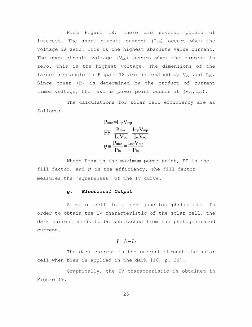
From Figure 18, there are several points of
interest. The short circuit current (ISC) occurs when the
voltage is zero. This is the highest absolute value current.
The open circuit voltage (VOC) occurs when the current is
zero. This is the highest voltage. The dimensions of the
larger rectangle in Figure 18 are determined by VOC and ISC.
Since power (P) is determined by the product of current
times voltage, the maximum power point occurs at (VMP,IMP).
The calculations for solar cell efficiency are as
follows:
max mp mp
max mp mp
sc oc sc oc
max mp mp
in in
P =I VP I VFF= =I V I V
P I V=P P
η ≡
Where Pmax is the maximum power point, FF is the
fill factor, and η is the efficiency. The fill factor
measures the “squareness” of the IV curve.
g. Electrical Output
A solar cell is a p-n junction photodiode. In
order to obtain the IV characteristic of the solar cell, the
dark current needs to be subtracted from the photogenerated
current.
L DI I I= −
The dark current is the current through the solar
cell when bias is applied in the dark [10, p. 30].
Graphically, the IV characteristic is obtained in
Figure 19.

26
Figure 19. Solar cell IV characteristic (From [21]).
C. CHAPTER CONCLUSIONS
This chapter provided basic information on
semiconductors and solar cells. The foundation has been
established from the physics stand point. The next step is
to cover an introduction to the simulation software.

27
III. SILVACO ATLAS SIMULATION SOFTWARE
This thesis uses Silvaco Atlas to perform solar cell
modeling. Silvaco International produces a suite of software
programs that together become a Virtual Wafer Fabrication
tool. This chapter introduces Silvaco Atlas and some of its
features.
A. VIRTUAL WAFER FAB
Silvaco International provides several software tools
to perform process and device simulation. From Figure 20, it
can be seen that Silvaco offers powerful simulation
software.
Figure 20. Silvaco’s Virtual Wafer Fabrication Environment
(From [22]).
In this thesis, Silvaco Atlas was extensively used. The
DeckBuild run-time environment received the input files.
Within the input files, Silvaco Atlas was called to execute
the code. And finally, TonyPlot was used to view the output
of the simulation. Additionally, output log files were
produced. The data extracted from the log files could then

28
be displayed using Microsoft Excel or Matlab scripts. Figure
21 shows the inputs and outputs for Silvaco Atlas.
Figure 21. Atlas inputs and outputs (From [23, p. 2-2]).
B. SILVACO ATLAS
Atlas is a software program used to simulate two and
three-dimensional semiconductor devices. The physical models
include in Atlas are presented in Table 6.

29
Table 6. Silvaco Atlas physical models (From [23, p. 1-2]).
C. INPUT FILE STRUCTURE
Silvaco Atlas receives input files through DeckBuild.
The code entered in the input file calls Atlas to run with
the following command:
go atlas
Following that command, the input file needs to follow
a pattern. The command groups are listed in Figure 22.

30
Figure 22. Atlas command groups and primary statements (From
[23, p. 2-8]).
Atlas follows the following format for statements and
parameters:
<STATEMENT> <PARAMETER>=<VALUE>
The following line of code serves as an example.
DOPING UNIFORM N.TYPE CONCENTRATION=1.0e16 REGION=1 \
OUTFILE=my.dop
The statement is DOPING. The parameters are UNIFORM,
N.TYPE, CONCENTRATION, REGION, and OUTFILE. There are four
different type of parameters: real, integer, character, and
logical. The back slash (\) serves the purpose of continuing
the code in the next line. Parameters, such as UNIFORM, are

31
logical. Unless a TRUE or FALSE value is assigned, the
parameter is assigned the default value. This value can be
either TRUE or FALSE. The Silvaco Atlas manual needs to be
referenced to identify the default value assigned to
specific parameters.
1. Structure Specification
The structure specification is done by defining the
mesh, the region, the electrodes and the doping levels.
a. Mesh
The mesh used for this thesis is two-dimensional.
Therefore, only x and y parameters are defined. The mesh is
a series of horizontal and vertical lines and spacing
between them. From Figure 23, the mesh statements are
specified.
Figure 23. Atlas mesh (From 2, p.18]).
32
The general format to define the mesh is:
X.MESH LOCATION=<VALUE> SPACING=<VALUE>
Y.MESH LOCATION=<VALUE> SPACING=<VALUE>
For example, the x.mesh starting at -250 microns
has spacing of 25 microns. That means it is relatively
coarse. The x.mesh becomes finer between -25 and 25 microns
with a spacing of 2.5 microns. The y.mesh is similarly
defined. For example, at y.mesh of -2.9 microns, the spacing
is 0.01 microns. Then at location y.mesh of -2.8 microns,
the spacing changes to 0.03 microns. The mesh is coarser at
y.mesh location of -1, when the spacing is 0.1.
A coarse or fine mesh determines the accuracy of
the simulation. A coarse mesh produces a faster simulation,
but less accurate results. A fine mesh produces a slower
simulation, but more accurate results. The areas that have a
finer mesh, therefore, are of greatest interest in the
simulation.
b. Region
After defining the mesh, it is necessary to define
the regions. The format to define the regions is as follows:
REGION number=<integer> <material_type> /
<position parameters>
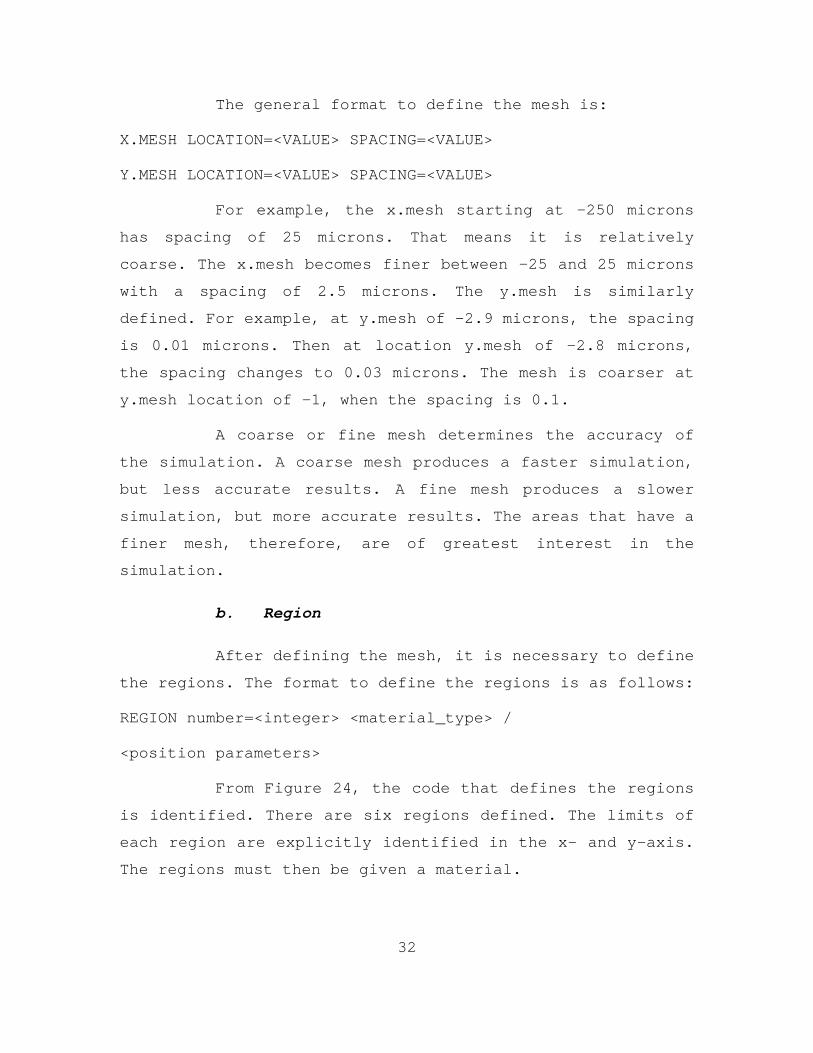
From Figure 24, the code that defines the regions
is identified. There are six regions defined. The limits of
each region are explicitly identified in the x- and y-axis.
The regions must then be given a material.
33
Figure 24. Atlas region (From [2, p. 19]).
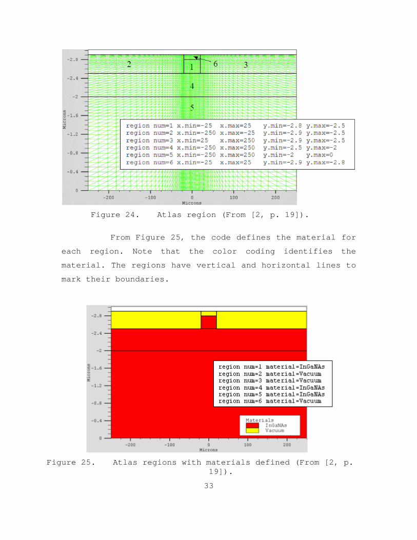
From Figure 25, the code defines the material for
each region. Note that the color coding identifies the
material. The regions have vertical and horizontal lines to
mark their boundaries.
Figure 25. Atlas regions with materials defined (From [2, p.
19]).

34
c. Electrodes
The next structure specification corresponds to
electrodes. Typically, in this simulation the only
electrodes defined are the anode and the cathode. However,
Silvaco Atlas has a limit of 50 electrodes that can be
defined. The format to define electrodes is as follows:
ELECTRODE NAME=<electrode name> <position_parameters>
From Figure 26, the electrode statements are
defined for the anode and the cathode. Note that the cathode
is defined with gold as the material. The x and y dimensions
correspond to region 6 previously defined. Meanwhile, the
anode is defined at the bottom of the cell for the entire x-
range at y=0.
Figure 26. Atlas electrodes (From [2, p. 20]).

35
d. Doping
The last aspect of structure specification that
needs to be defined is doping. The format of the Atlas
statement is as follows:
DOPING <distribution type> <dopant_type> /
<position parameters>
From Figure 27, the doping types and the doping
levels are defined. Doping can be n-type or p-type. The
distribution type can be uniform or Gaussian.
Figure 27. Atlas doping (From [2, p. 21]).
2. Materials Model Specification
After the structure specification, the materials model
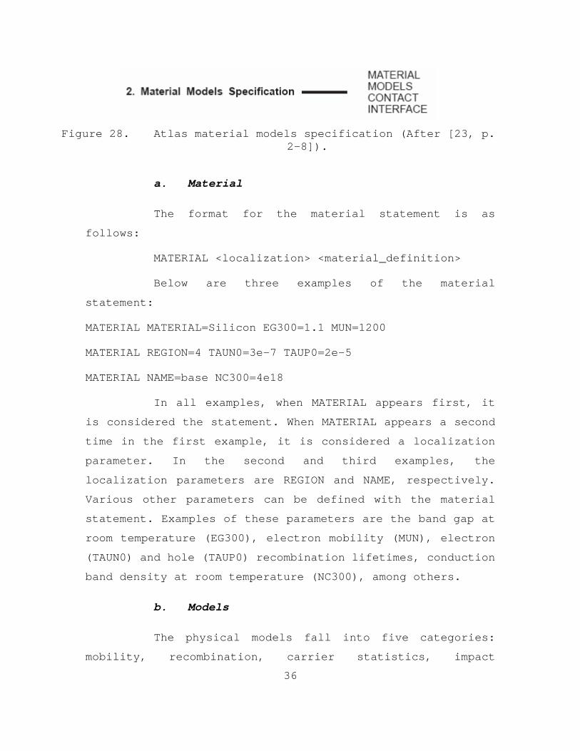
specification is next. From Figure 28, the materials model
specification is broken down into material, models, contact,
and interface.
36
Figure 28. Atlas material models specification (After [23, p.
2-8]).
a. Material
The format for the material statement is as
follows:
MATERIAL <localization> <material_definition>
Below are three examples of the material
statement:
MATERIAL MATERIAL=Silicon EG300=1.1 MUN=1200
MATERIAL REGION=4 TAUN0=3e-7 TAUP0=2e-5
MATERIAL NAME=base NC300=4e18
In all examples, when MATERIAL appears first, it
is considered the statement. When MATERIAL appears a second
time in the first example, it is considered a localization
parameter. In the second and third examples, the
localization parameters are REGION and NAME, respectively.
Various other parameters can be defined with the material
statement. Examples of these parameters are the band gap at
room temperature (EG300), electron mobility (MUN), electron
(TAUN0) and hole (TAUP0) recombination lifetimes, conduction
band density at room temperature (NC300), among others.
b. Models
The physical models fall into five categories:
mobility, recombination, carrier statistics, impact

37
ionization, and tunneling. The syntax of the model statement
is as follows:
MODELS <model flag> <general parameter> /
<model dependent parameters>
The choice of model depends on the materials
chosen for simulation.
The example below activates several models.
MODELS CONMOB FLDMOB SRH
CONMOB is the concentration dependent model.
FLDMOB is the parallel electric field dependence model. SRH
is the Shockley-Read-Hall model.
c. Contact
Contact determines the attributes of the
electrode. The syntax for contact is as follows:
CONTACT NUMBER=<n> |NAME=<ename>|ALL
The following is an example of the contact
statement.
CONTACT NAME=anode current
d. Interface
The semiconductor or insulator boundaries are
determined with the interface statement. The syntax is as
follows:
INTERFACE [<parameters>]
The following example shows the usage of the
interface statement.

38
INTERFACE X.MIN=-4 X.MAX=4 Y.MIN=-0.5 Y.MAX=4 \
QF=1e10 S.N=1e4 S.P=1e4
The max and min values determine the boundaries.
The QF value specifies the fixed oxide charge density (cm-
2). The S.N value specifies the electron surface
recombination velocity. S.P is similar to S.N, but for
holes.
3. Numerical Method Selection
After the materials model specification, the numerical
method selection must be specified. From Figure 29, the only
statement that applies to numerical method selection is
method.
Figure 29. Atlas numerical method selection (After [23, p. 2-
8]).
There are various numerical methods to calculate
solutions to semiconductor device problems. There are three
types of solution techniques used in Silvaco Atlas:
• decoupled (GUMMEL)
• fully coupled (NEWTON)
• BLOCK
The GUMMEL method solves for each unknowns by keeping
all other unknowns constant. The process is repeated until
there is a stable solution. The NEWTON method solves all

39
unknowns simultaneously. The BLOCK method solves some
equations with the GUMMEL method and some with the NEWTON
method.
The GUMMEL method is used for a system of equations
that are weakly coupled and there is linear convergence. The
NEWTON method is used when equations are strongly coupled
and there is quadratic convergence.
The following example shows the use of the method
statement.
METHOD GUMMEL NEWTON
In this example, the equations are solved with the
GUMMEL method. If convergence is not achieved, then the
equations are solved using the NEWTON method.
4. Solution Specification
After completing the numerical method selection, the
solution specification is next. Solution specification is
broken down into log, solve, load, and save statements, as
shown in Figure 30.
Figure 30. Atlas solution specification (After [23, p. 2-8]).
a. Log
LOG saves all terminal characteristics to a file.
DC, transient, or AC data generated by a SOLVE statement
after a LOG statement is saved.

40
The following shows an example of the LOG
statement.
LOG OUTFILE=myoutputfile.log
The example saves the current-voltage information
into myoutputfile.log.
b. Solve
The SOLVE statement follows the LOG statement.
SOLVE performs a solution for one or more bias points. The
following is an example of the SOLVE statement.
SOLVE B1=10 B3=5 BEAM=1 SS.PHOT SS.LIGHT=0.01 \
MULT.F FREQUENCY=1e3 FSTEP=10 NFSTEP=6
B1 and B3 specify the optical spot power
associated with the optical beam numbers 1 and 3,
respectively. The beam number is an integer between 1 and
10. BEAM is the beam number of the optical beam during AC
photogeneration analysis. SS.PHOT is the small signal AC
analysis. SS.LIGHT is the intensity of the small signal part
of the optical beam during signal AC photogeneration
analysis. MULT.F is the frequency to be multiplied by FSTEP.
NFSTEPS is the number of times that the frequency is
incremented by FSTEP.
c. Load and Save
The LOAD statement enters previous solutions from
files as initial guess to other bias points. The SAVE
statement enters all node point information into an output
file.

41
The following are examples of LOAD and SAVE
statements.
SAVE OUTF=SOL.STR
In this case, SOL.STR has information saved after
a SOLVE statement. Then, in a different simulation, SOL.STR
can be loaded as follows:
LOAD INFILE=SOL.STR
5. Results Analysis
Once a solution has been found for a semiconductor
device problem, the information can be displayed graphically
with TonyPlot. Additionally, device parameters can be
extracted with the EXTRACT statement, as shown in Figure 31.
Figure 31. Atlas results analysis (After [23, p. 2-8]).
In the example below, the EXTRACT statement obtains the
current and voltage characteristics of a solar cell. This
information is saved into the IVcurve.dat file. Then,
TonyPlot plots the information in the IVcurve.dat file.
EXTRACT NAME="iv" curve(v."anode", I."cathode") / OUTFILE="IVcurve.dat" TONYPLOT IVcurve.dat
Figure 32 shows the sample IV curve plotted by
TonyPlot.

42
Figure 32. Sample TonyPlot IV curve.
D. CONCLUSION
This chapter presented an introduction to Silvaco
Atlas, the structure of the input files, and some of its
statements. With these basic tools, the next chapter
introduces some basic information on wurtzite Indium Gallium
Nitride before proceeding to the thesis simulation.

43
IV. INDIUM GALLIUM NITRIDE
A. A FULL SPECTRUM PHOTOVOLTAIC MATERIAL
Prior to 2001, it was thought that wurtzite Indium
Nitride had a band gap of approximately 1.9 eV. In 2001, it
was discovered that Indium Nitride had a much smaller band
gap. Davydov, et al., concluded in [24] that Indium Nitride
had a band gap of approximately 0.9 eV. Additionally,
Davydov, et al., presented in [25] that wurtzite Indium
Gallium Nitride band gaps in the range x=0.36 to x=1
supported findings in [24]. The band gaps for Indium Gallium
Nitride, with Indium Nitride concentrations ranging from 0.0
to 1.0 are presented in Figure 33.
Figure 33. InGaN band gap as a function of In composition
(After [25]).

44
Later on, research conducted at Lawrence Berkeley
National Laboratory presented that the Indium Nitride
fundamental band gap was approximately 0.77 eV at room
temperature. Since Gallium Nitride has a band gap of
approximately 3.4 eV at room temperature, then Indium
Gallium Nitride can have a band gap ranging from 0.77 eV to
3.4 eV by changing the percent composition of Indium and
Gallium within Indium Gallium Nitride. Figure 34 confirms
that Indium Gallium Nitride follows the pattern of ranging
from 0.77 eV to 3.4 eV.
Figure 34. InGaN band gap and solar spectrum comparison
(After [26]).
Figure 34 also presents the solar spectrum on the left-
hand side. Therefore, it is clear that the visible spectrum
has a near-perfect match with the Indium Gallium Nitride
range of band gaps.
It should be noted that research conducted in [27]
presents a Indium Nitride band gap of 1.7± 0.2 eV. It is
stated in [27], “These investigations clarify that a band

45
transition around 1.7 eV does exist in wurtzite InN although
in this energy range optical material responses are hardly
ever found. If the 1.7 eV band transition is indeed the
fundamental bandgap in InN at room temperature it is
concluded that defect bands, grain boundaries, dislocations
and/or the very conductive surface are contributing to the
lower energy optical responses in InN. The identification of
the various defects in InN will be subject of future
investigations.”
In follow up research, [28] explains the possible
reason for the higher Indium Nitride band gap: “Owing to
InN’s exceptional propensity for n-type activity, in many
instances the larger apparent values of the band gap can be
attributed to the Burstein–Moss shift of the optical
absorption edge resulting from the occupation of conduction
band states by free electrons.”
Figure 35 shows evidence that the fundamental band gap
of indium nitride is approximately 0.7 eV, and not near 2
eV. The optical absorption (blue curve) has an onset at
approximately 0.8 eV. There is no change in absorption
around the 2 eV range. The photo luminescence (red curve)
shows a peak at the band edge of approximately 0.8 eV.
Finally, the photo-modulated reflectance (green curve)
presents a transition close to 0.8 eV. These three curves
support a band gap for indium nitride of approximately 0.8
eV. The 1.9-2.0 eV band gap is not evident in Figure 35.

46
Figure 35. Evidence of 0.7 eV band gap for indium nitride
(From [29]).
The controversy about indium nitride’s fundamental band
gap is not the subject of this thesis. This research
proceeded accepting the fundamental band gap of 0.77 eV for
indium nitride.
According to [30], the following formula provides an
approximation of Indium Gallium Nitride band gap:
( ) 3.42 0.77(1 ) 1.43 (1 )GE x x x x x= + − − −
Where EG is the InGaN band gap, 3.42 eV is the GaN band
gap, 0.77 eV is the InN band gap, 1.43 eV is the bowing
parameter b, x is the Ga concentration, and (1-x) is the In
concentration.
When plotting the band gap formula for InGaN using a
Matlab script, the Figure 36 is obtained.

47
Figure 36. InGaN band gap as a function of In concentration.
The band gaps used in the Silvaco Atlas simulations
were found by modifying the Matlab script for Figure 35.
B. RADIATION-HARD SEMICONDUCTOR MATERIAL
Radiation-hard materials are essential for space
applications. When compared to other Gallium Arsenide and
Indium Gallium Phosphide, Indium Gallium Nitride is able to
withstand a greater amount of radiation. According to [31],
InGaN “retains its optoelectronic properties at radiation
damage doses at least two orders of magnitude higher than
the damage thresholds of the materials (GaAs and GaInP)
currently used in high efficiency MJ cells”. Radiation
levels in [31] were 1 MeV electron, 2 MeV proton, and 2 MeV
alpha particle irradiation.

48
This indicates that InGaN is not only potentially a
high-efficiency photovoltaic material, but it is also able
to withstand the harsh space environment.
C. INDIUM GALLIUM NITRIDE CHALLENGES
There are some significant issues that currently
prevent InGaN from being used as photovoltaic material. As
of this writing, no PN junction has been built. The PN
junction is essential to create photodiodes. Indium Nitride
has the highest electron affinity among all semiconductors
[32]. Hence, Indium Nitride has a tendency to be n-type. It
is much more difficult to build p-type material with Indium
Nitride. However, evidence of p-type doping in Indium
Nitride and Indium Gallium Nitride has been reported in [33]
using Magnesium. This is a step in the right direction.
Further progress in this area dictates the creation of
Indium Gallium Nitride PN junctions.
Having reviewed the characteristics of Indium Gallium
Nitride, the next chapter covers the simulation of Indium
Gallium Nitride using Silvaco Atlas.

49
V. SIMULATION OF INDIUM GALLIUM NITRIDE IN SILVACO ATLAS
One of the primary motivations behind this research was
to find a way to make solar cells significantly more
efficient. When researching high-efficiency solar cells, the
improvements were typically incremental over previous
results. Solar cells were first designed as single-junction.
The most popular photovoltaic material has been Silicon due
to its abundance and relatively low cost. The maximum
efficiency of polycrystalline Silicon is approximately
19.8%. Commercial silicon solar cells have a maximum
efficiency of approximately 13%. Improvements in efficiency
can be obtained in single-junction solar cells by using
Gallium Arsenide. Monocrystalline Gallium Arsenide has a
maximum efficiency of approximately 25.1% [10, p. 195].
By designing dual-junction solar cells, the efficiency
can again be improved. A dual-junction cell with Gallium
Phosphide as the top junction and Gallium Arsenide as the
bottom cell can have an efficiency of 30.3% [10, p 302].
Increasing the number of junctions makes the cells more
complex in design and the gains begin to diminish. Triple-
junction cells have efficiencies of approximately 31%. Quad-
junction cells have efficiencies of approximately 33%. It is
expected that five- and six-junction solar cells can have
efficiencies of approximately 35% [36].
This simulation uses Indium Gallium Nitride as
photovoltaic material in a simulation. With its full-
spectrum characteristics, the efficiency of Indium Gallium
Nitride has the potential to surpass previous results.

50
A. SINGLE-JUNCTION SOLAR CELL
Figure 37 shows a graphical representation of the
single junction solar cell. The thickness of the emitter is
0.01 mµ and the doping is 1x10¹⁶/cm3. The thickness of the
base is 3 mµ and the doping is 1x10¹⁶/cm3.
Figure 37. Simple single-junction InGaN solar cell.
The first step is to develop single junction solar
cells. Optical data in the form of dielectric constants was
found in [34] for In0.20Ga0.80N. This corresponds to a
calculated band gap of 2.66 eV. Additional optical data was
found in [35] for In0.57Ga0.43N (calculated Eg=1.60 eV),
In0.68Ga0.32N (calculated Eg=1.31 eV), and In0.78Ga0.22N
(calculated Eg=1.1 eV). The dielectric constants were then
converted to index of refraction (n) and extinction
coefficient (k) using a Matlab script (Appendix B). The band
gap and the optical data were entered into the input deck.
The simulation ran in Silvaco Atlas. From the log file, the
current and voltage data was extracted.
In the single-junction case, each of the cells had AM0
as the input spectrum. Figure 38 shows the IV curves of four
single-junction solar cells. The IV curve pattern
corresponds to empirical findings of other multijunction
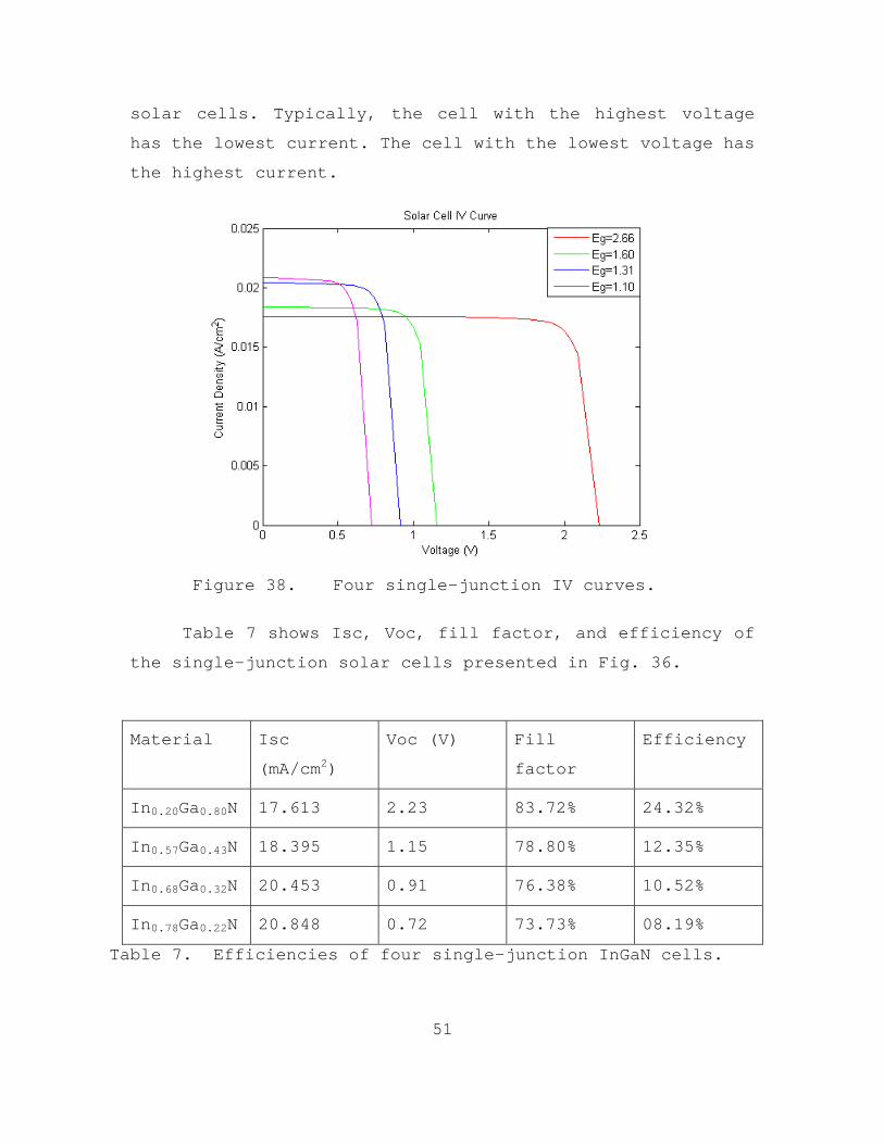
51
solar cells. Typically, the cell with the highest voltage
has the lowest current. The cell with the lowest voltage has
the highest current.
Figure 38. Four single-junction IV curves.
Table 7 shows Isc, Voc, fill factor, and efficiency of
the single-junction solar cells presented in Fig. 36.
Material Isc
(mA/cm2)
Voc (V) Fill
factor
Efficiency
In0.20Ga0.80N 17.613 2.23 83.72% 24.32%
In0.57Ga0.43N 18.395 1.15 78.80% 12.35%
In0.68Ga0.32N 20.453 0.91 76.38% 10.52%
In0.78Ga0.22N 20.848 0.72 73.73% 08.19%
Table 7. Efficiencies of four single-junction InGaN cells.

52
The efficiencies shown in Table 7 indicate that a high-
efficiency, single-junction cell with In0.20Ga0.80N has good
prospects. A 24.32% efficiency compares favorably to the
single-junction Gallium Arsenide efficiency of 25.1%. The
InGaN cells simulated can be optimized by changing the
thickness of the junction and changing the doping levels.
Adding a window, a back surface field (BSF) and a buffer can
also help in improving the efficiency results. These
improvements can be the subject of future research.
B. DUAL-JUNCTION SOLAR CELL
Figure 39 shows a graphical representation of a dual-
junction InGaN solar cell. The thicknesses and doping levels
remain identical to the single-junction case.
Figure 39. Simple dual-junction InGaN solar cell.
From the discussion in the single-junction solar cell
section, it should be clear that the best combination of
InGaN band gaps is 2.66 eV and 1.60 eV, since they have the

53
highest efficiencies. It should be noted that for this
simulation, the AM0 spectrum was provided for the top
junction In0.20Ga0.80N (Eg=2.66 eV). The bottom junction
In0.57Ga0.43N (Eg=1.60 eV) received the AM0 spectrum minus the
spectrum absorbed by the top cell.
Figure 40 shows the IV curves of the dual-junction
solar cell. Note that compared to Figure 38, the IV curve of
Eg=2.66 eV stayed the same, while the IV curve of Eg=1.60 eV
had a current drop. This current decrease was expected
because the input spectrum was diminished by the top cell.
Figure 40. Dual-junction InGaN solar cell IV curve.
Since the junctions are in series, the overall IV curve
is limited in its current level by the IV curve with the
lowest current. The voltages are added accordingly.
Table 8 shows the efficiency of the dual-junction solar
cell.

54
Material Isc
(mA/cm2)
Voc (V) Fill
factor
Efficiency
In0.20Ga0.80N
In0.57Ga0.43N
Dual
junction
17.11 3.38 83.25% 35.58%
Table 8. Dual-junction InGaN efficiency.
There is a significant increase in efficiency from
single-junction (24.32%) to dual junction (35.58%) InGaN
solar cells. This improvement alone should be enough to
continue to pursue the development of InGaN solar cells.
Searching for further improvements, three- and four-
junction solar cells are examined next.
C. THREE-JUNCTION SOLAR CELL
Figure 41 shows a graphical representation of a three-
junction InGaN solar cell. Thicknesses and doping levels
stayed the same as the single- and dual-junction cases. From
the single-junction solar cell discussion, the three most
efficient cells were selected (Eg=2.66 eV, Eg=1.60 eV,
Eg=1.31 eV). The top cell In0.20Ga0.80N (Eg=2.66 eV) received
the AM0 spectrum. The cell In0.57Ga0.43N (Eg=1.60 eV) received
the AM0 spectrum minus the spectrum absorbed by the top
cell. The cell In0.68Ga0.32N (Eg=1.31 eV) received the AM0
spectrum minus the spectrum absorbed by the top two cells.
Figure 42 shows the IV curve of the three-junction
solar cell. Note that the current level of the top two cells
is identical to the dual-junction case. However, the current

55
level of the bottom cell is lower than the single junction
case for the same concentration. Similarly to the dual-
junction case, the current of the overall IV curve is
limited by the individual junction with the lowest IV curve.
The voltages are added accordingly, since the three
junctions are in series.
Figure 41. Simple three-junction InGaN solar cell.

56
Figure 42. Three-junction InGaN solar cell IV curve.
Table 9 shows the efficiency of the three-junction
InGaN solar cell.
Material Isc
(mA/cm2)
Voc (V) Fill
factor
Efficiency
In0.20Ga0.80N
In0.57Ga0.43N
In0.68Ga0.32N
Three
junction
14.12 4.27 87.23% 38.90%
Table 9. Three-junction InGaN efficiency
The increase in efficiency from dual-junction to three-
junction is 35.58% to 38.90%. The modest increase in
efficiency can be attributed to the drop in Isc from 17.11

57
mA/cm2 to 14.12 mA/cm2. However, the increase in Voc from
3.38 V to 4.27 ensured that the efficiency would increase.
The last case to be examined is the quad-junction InGaN
solar cell.
D. QUAD-JUNCTION SOLAR CELL
Figure 43 shows a graphical representation of a quad-
junction InGaN solar cell. Thicknesses and doping levels
remained the same as the single-, dual-, and three-junction
cases. Spectrum input followed the pattern of the dual- and
three-junction cases. As expected, the current dropped for
all cases where AM0 had been reduced by the top cells.
Figure 44 shows the IV curve for a quad-junction InGaN
solar cell. Note that the IV-curves for the top three cells
are identical to the three-junction case. The bottom cell
has a lower current level compared to the single junction
case.
Table 10 shows the efficiency of the quad-junction
InGaN solar cell.

58
Figure 43. Simple quad-junction InGaN solar cell

59
Figure 44. Quad-junction InGaN solar cell IV curve
Material Isc
(mA/cm2)
Voc (V) Fill
factor
Efficiency
In0.20Ga0.80N
In0.57Ga0.43N
In0.68Ga0.32N
In0.78Ga0.22N
Quad-
junction
12.88 4.98 87.86% 41.69%
Table 10. Quad junction InGaN efficiency
For completeness, efficiency calculations are provided
below for the quad-junction case. These calculations were
performed with the help of a Matlab script.
60
max mp mp 2 2
2max mp mp
sc oc sc oc2
2max mp mp
in in2
A WP =I V =(0.0126 )(4.4736 V)=0.0564cm cm
W0.0564P I V cmFF= = = =87.86%AI V I V (0.0129 )(4.9793V)cm
W0.0564P I V cmη = = =0.4169=41.69%WP P 0.1353cm
≡
In order to get a perspective on how this result
compares to actual solar cells in production, Figure 45 is
presented.
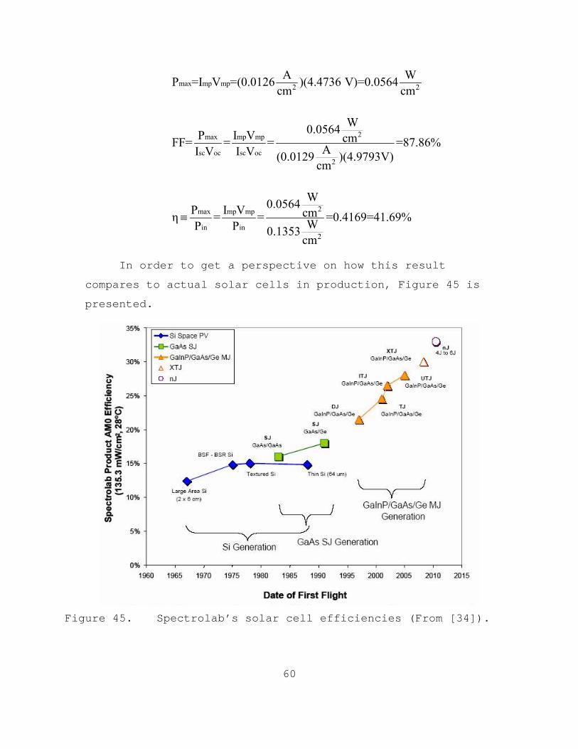
Figure 45. Spectrolab’s solar cell efficiencies (From [34]).

61
The label nJ stands for new generation four to six-
junction cells. XTJ is a designation for a triple junction
cell. UTJ stands for Ultra Triple Junction. ITJ means
Improved Triple Junction. TJ is Triple Junction. DJ is Dual
Junction. SJ is single junction.
Figure 45 shows the efficiency progression of a leading
solar cell manufacturer (Spectrolab). The first step
consists of single junction silicon solar cells. These cells
were in production from the mid-1960s until the early 1990s.
Their efficiency was close to 15%. The next step consisted
of single junction gallium arsenide solar cells. These cells
had efficiencies between 15% and 20%. In the mid-1990s, dual
junction solar cells appeared. Efficiencies were slightly
above 20%. Triple junction cells appeared in the early 2000s
with efficiencies nearing 30%. The projections are to
produce quad-junction solar cells within the next decade
with efficiencies just under 35%.
Further comparisons can be made with another
simulation. Modeling in [5] used physics equations to
calculate Isc and Voc. The input spectrum used in that
simulation was AM1.5 instead of AM0. The InGaN band gap
formula used was from [37]. This thesis used the band gap
formula from [30]. Figure 46 shows a comparison of the two
formulas. Both formulas seek to duplicate findings from
actual band gap measurements. Therefore, both formulas are
approximations only.
The simulation from [5] obtained the results presented
in Table 11. The highest efficiency obtained in that
simulation is 40.346% with a six-junction InGaN solar cell.

62
Figure 46. Comparison of InGaN band gap formulas
Table 11. InGaN efficiency results (From [5]).
The differences in efficiency results can be partly
attributed to the difference in band gap formula used. For
example, In0.20Ga0.80N has a band gap of 2.66 eV with the
formula used in this thesis. The formula from [37] yields a
band gap of 1.897 eV. If the In0.20Ga0.80N band gap of 1.897
eV is substituted in the single-junction solar cell
simulation of this thesis, the efficiency decreases
significantly. Figure 47 compares the IV output for
In0.20Ga0.80N at Eg=1.897 eV and Eg=2.66 eV.

63
Figure 47. IV curve for In0.20Ga0.80N using different band gaps
The efficiency of the In0.20Ga0.80N (2.66 eV) single-
junction solar cell simulated in this thesis was 24.32%.
Changing the band gap to 1.897 eV yields an efficiency of
14.94%. This is a significant decrease. However, the band
gap for the other three junctions increases with the formula
used in [37]. The quad-junction simulation was run with the
new band gaps. Figure 48 shows the IV curve for the quad-
junction solar cell. The efficiency for the quad-junction
solar cell increases to 43.62%. It is difficult to state
which band gap model is more correct.

64
Figure 48. Quad-junction InGaN solar cell IV curve using
calculated band gaps from [37] formula.
Material Isc
(mA/cm2)
Voc (V) Fill
factor
Efficiency
In0.20Ga0.80N
In0.57Ga0.43N
In0.68Ga0.32N
In0.78Ga0.22N
Quad-
junction
12.9 5.194 88.06% 43.62
Table 12. Quad junction InGaN efficiency using band gaps from [37] calculations.

65
A common finding in [5] and this thesis is that both
simulations show that Indium Gallium Nitride multijunction
solar cells can provide a significant improvement in solar
cell efficiency. However, this is the first time that a
Technology Computer Aided Design (TCAD), such as Silvaco
Atlas, has been used to simulate InGaN solar cells.
The results of this thesis simulation demonstrate that
Indium Gallium Nitride is potentially an excellent
semiconductor photovoltaic material. The material science
research in the future can confirm these outcomes in the
future.
Production of single-junction solar cells appears to be
the first step to be taken. Once the photovoltaic properties
are demonstrated with actual Indium Gallium Nitride, the
complexity of dual-junction solar cells can be addressed.
Tunnel junctions made up of Indium Gallium Nitride may need
to be explored as well.

66
THIS PAGE LEFT INTENTIONALLY BLANK

67
VI. CONCLUSIONS AND RECOMMENDATIONS
A. RESULTS AND CONCLUSIONS
Indium Gallium Nitride is a semiconductor material with
potential to be used in photovoltaic devices. A new
simulation was performed using Silvaco Atlas. The results of
the quad-junction Indium Gallium Nitride solar cell indicate
that a new high-efficiency material should be produced.
Current state-of-the-art multijunction solar cells have
efficiencies in the 30-33% range. The 41% efficiency
predicted in this thesis is the highest of all simulations
performed at the Naval Postgraduate School using Silvaco
Atlas.
B. RECOMMENDATIONS FOR FUTURE RESEARCH
There are multiple areas that can be explored in future
research. This thesis focused on the development of a solar
cell model that emphasizes the use of optical constants
(refraction and extinction coefficients n and k). The model
used default settings for other parameters, such as
permittivity, affinity, radiative recombination rate,
electron and hole lifetimes, electron and hole density of
states, and lattice constants. One area of future research
is to obtain measured data for the above parameters. This
subject is critical in improving the model. The other option
is to interpolate from known values. Additionally, the
inclusion of tunnel junctions in the simulation is of great
value.

68
Other areas of research include finding different
semiconductor materials that offer potential for high-
efficiency solar cells. Lawrence Berkeley National
Laboratory is also working with multiband materials, such as
Zinc Manganese Tellerium Oxide (ZnMnTeO). This type of
material offers a single junction solar cell, but there are
multiple band gaps within the single junction.
One more recommended path is to optimize the physical
parameters of the solar cell. The thickness of each of the
layers can be optimized to produce a better efficiency. The
band gap distribution for a quad-junction solar cell can be
improved to obtain higher efficiency. It should be noted
that obtaining the correct optical data for these band gaps
is essential.

69
APPENDIX A: SILVACO ATLAS INPUT DECK
The code for the quad-junction InGaN solar cell was
broken down into four single-junction solar cells. This was
done because the material properties of InGaN had to be
changed for each of the junctions.
Original code for the Silvaco Atlas input deck was
obtained from Michalopolous [1], Bates, [2], Green [3], and
Canfield [4]. Modifications to the code were made to support
this thesis.
A. TOP JUNCTION: IN0.20GA0.80N, EG=2.66 EV
go atlas set cellWidth=5.000000e+002 set capWidthpercent=8.000000e+000 set divs=1.000000e+001 set contThick=1.000000e-001 set capThick=3.000000e-001 set capDop=1.000000e+020 set windowThick=0.01 set winDop=2.15e17 set emitterThick=0.01 #changed emitDop from 1e16 to 1e20 set emitDop=1e16 set baseThick=3.19467 #changed basDop from 1e16 to 1e20 set baseDop=1e16 set bsfThick=0.03533 set bsfDop=2.15e19 set cellWidthDiv=$cellWidth/$divs set width3d=100e6/$cellWidth set capWidth=0.01*$capWidthpercent*$cellWidth/2 set capWidthDiv=$capWidth/($divs/2) set cellWidthHalf=$cellWidth/2 set bsfLo=0 set bsfHi=$bsfLo-$bsfThick set bsfDiv=$bsfThick/$divs set baseLo=$bsfHi set baseHi=$baseLo-$baseThick set baseMid=$baseLo-$baseThick/2 set baseDiv=$baseThick/$divs set emitterLo=$baseHi

70
set emitterHi=$emitterLo-$emitterThick set emitterDiv=$emitterThick/$divs set windowLo=$emitterHi set windowHi=$windowLo-$windowThick set windowDiv=$windowThick/$divs set capLo=$windowHi set capHi=$capLo-$capThick #set capDiv=$capThick/$divs set contLo=$capHi set contHi=$contLo-$contThick set contDiv=$contThick/$divs set lightY=$emitterHi-5 mesh width=$width3d ## X-Mesh x.mesh loc=-$cellWidthHalf spac=$cellWidthDiv x.mesh loc=-$capWidth spac=$capWidthDiv x.mesh loc=$capWidth spac=$capWidthDiv x.mesh loc=$cellWidthHalf spac=$cellWidthDiv ## Y-Mesh # Top contact y.mesh loc=$contHi spac=0 y.mesh loc=$contLo spac=0 # Cap # Window y.mesh loc=$windowHi spac=$windowDiv y.mesh loc=$windowLo spac=$windowDiv # Emitter y.mesh loc=$emitterLo spac=$emitterDiv # Base y.mesh loc=$baseMid spac=$baseDiv # BSF y.mesh loc=$bsfHi spac=$bsfDiv y.mesh loc=$bsfLo spac=$bsfDiv ## Regions # Cap #region num=8 material=Vacuum x.min=-$capWidth x.max=$capWidth y.min=$contHi y.max=$contLo region num=1 material=InGaN x.min=-$capWidth x.max=$capWidth y.min=$capHi y.max=$capLo x.comp=0.20 region num=2 material=Vacuum x.min=-$cellWidthHalf x.max=-$capWidth y.min=$contHi y.max=$capLo region num=3 material=Vacuum x.min=$capWidth x.max=$cellWidthHalf y.min=$contHi y.max=$capLo # Window [for Ge cell, use AlGaAs with x.comp=0.2] region num=4 material=InGaN x.min=-$cellWidthHalf x.max=$cellWidthHalf y.min=$windowHi y.max=$windowLo x.comp=0.20 #region num=4 material=AlGaAs x.comp=0.2 x.min=-$cellWidthHalf x.max=$cellWidthHalf y.min=$windowHi y.max=$windowLo # Emitter region num=5 material=InGaN x.min=-$cellWidthHalf x.max=$cellWidthHalf y.min=$emitterHi y.max=$emitterLo x.comp=0.20 # Base

71
region num=6 material=InGaN x.min=-$cellWidthHalf x.max=$cellWidthHalf y.min=$baseHi y.max=$baseLo x.comp=0.20 # BSF region num=7 material=InGaN x.min=-$cellWidthHalf x.max=$cellWidthHalf y.min=$bsfHi y.max=$bsfLo x.comp=0.20 ## Electrodes [for InGaP cell, add cathode (gold) and remove cathode (conductor)] electrode name=cathode material=Gold x.min=-$capWidth x.max=$capWidth y.min=$contHi y.max=$contLo #electrode name=cathode x.min=-$cellWidthHalf x.max=$cellWidthHalf y.min=$windowHi y.max=$windowHi electrode name=anode x.min=-$cellWidthHalf x.max=$cellWidthHalf y.min=$bsfLo y.max=$bsfLo ## Doping [for InGaP cell, uncomment cap doping] # Cap doping uniform region=1 n.type conc=$capDop # Window doping uniform region=4 n.type conc=$winDop # Emitter doping uniform region=5 n.type conc=$emitDop # Base doping uniform region=6 p.type conc=$baseDop # BSF doping uniform region=7 p.type conc=$bsfDop ## Material properties # Opaque contact [comment out for InGaP cell] #material region=8 real.index=1.2 imag.index=1.8 # Vacuum (for zero reflection) [change to match window material (InGaP use Vacuum_AlInP)] # [for InGaP cell, comment out region 1] #material region=1 index.file=Vacuum_InGaP.opt material region=2 index.file=VacuumIn20Ga80N.opt material region=3 index.file=VacuumIn20Ga80N.opt #InGaN material material=InGaN EG300=2.6612 index.file=In20Ga80N.opt # Gold material material=Gold real.index=1.2 imag.index=1.8 ## Models [InGaP cell, 1; GaAs cell, 5&6; InGaNAs cell, 7] models region=1 CONMOB MODELS CHUANG CONMOB FLDMOB SRH OPTR PRINT ## Light beams [GaAs b1,0.55-0.75,200 b2,0.75-0.88,65] 0.12-2.7,50 [630,825] beam num=1 x.origin=0 y.origin=$lightY angle=90 back.refl power.file=AM0nrel.spec \ wavel.start=0.12 wavel.end=2.4 wavel.num=50 struct outfile=SingleCell_webf.str #tonyplot SingleCell_webf.str solve init method gummel newton maxtraps=10 itlimit=25 solve b1=0.9 ## Getting Isc for I-V curve points method newton maxtraps=10 itlimit=100
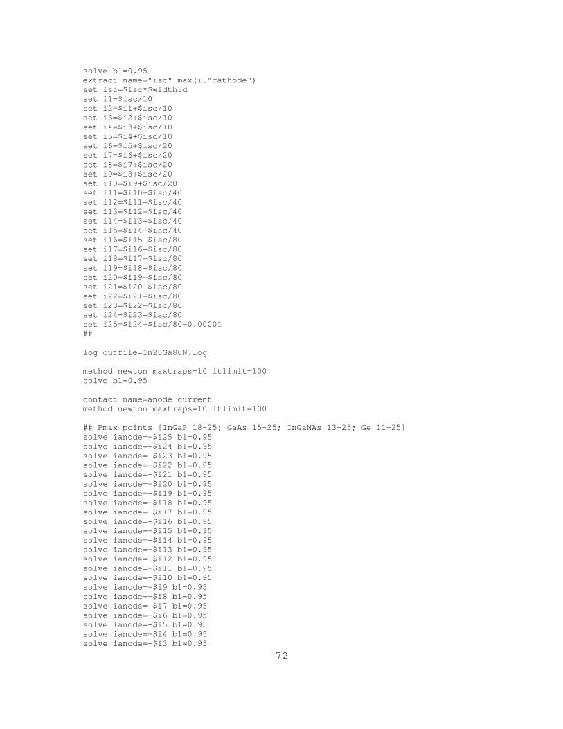
72
solve b1=0.95 extract name="isc" max(i."cathode") set isc=$isc*$width3d set i1=$isc/10 set i2=$i1+$isc/10 set i3=$i2+$isc/10 set i4=$i3+$isc/10 set i5=$i4+$isc/10 set i6=$i5+$isc/20 set i7=$i6+$isc/20 set i8=$i7+$isc/20 set i9=$i8+$isc/20 set i10=$i9+$isc/20 set i11=$i10+$isc/40 set i12=$i11+$isc/40 set i13=$i12+$isc/40 set i14=$i13+$isc/40 set i15=$i14+$isc/40 set i16=$i15+$isc/80 set i17=$i16+$isc/80 set i18=$i17+$isc/80 set i19=$i18+$isc/80 set i20=$i19+$isc/80 set i21=$i20+$isc/80 set i22=$i21+$isc/80 set i23=$i22+$isc/80 set i24=$i23+$isc/80 set i25=$i24+$isc/80-0.00001 ## log outfile=In20Ga80N.log method newton maxtraps=10 itlimit=100 solve b1=0.95 contact name=anode current method newton maxtraps=10 itlimit=100 ## Pmax points [InGaP 18-25; GaAs 15-25; InGaNAs 13-25; Ge 11-25] solve ianode=-$i25 b1=0.95 solve ianode=-$i24 b1=0.95 solve ianode=-$i23 b1=0.95 solve ianode=-$i22 b1=0.95 solve ianode=-$i21 b1=0.95 solve ianode=-$i20 b1=0.95 solve ianode=-$i19 b1=0.95 solve ianode=-$i18 b1=0.95 solve ianode=-$i17 b1=0.95 solve ianode=-$i16 b1=0.95 solve ianode=-$i15 b1=0.95 solve ianode=-$i14 b1=0.95 solve ianode=-$i13 b1=0.95 solve ianode=-$i12 b1=0.95 solve ianode=-$i11 b1=0.95 solve ianode=-$i10 b1=0.95 solve ianode=-$i9 b1=0.95 solve ianode=-$i8 b1=0.95 solve ianode=-$i7 b1=0.95 solve ianode=-$i6 b1=0.95 solve ianode=-$i5 b1=0.95 solve ianode=-$i4 b1=0.95 solve ianode=-$i3 b1=0.95

73
solve ianode=-$i2 b1=0.95 solve ianode=-$i1 b1=0.95 solve ianode=0 b1=0.95 log off extract name="iv" curve(v."anode", i."cathode") outfile="IVcurveIn20Ga80N.dat" tonyplot IVcurveIn20Ga80N.dat log outfile=doneIn20Ga80N.log log off
B. SECOND JUNCTION: IN0.57GA0.43N, EG=1.6 EV
go atlas set cellWidth=5.000000e+002 set capWidthpercent=8.000000e+000 set divs=1.000000e+001 set contThick=1.000000e-001 set capThick=3.000000e-001 set capDop=1.000000e+020 set windowThick=0.01 set winDop=2.15e17 set emitterThick=0.01 #changed emitDop from 1e16 to 1e20 set emitDop=1e16 set baseThick=3.19467 #changed basDop from 1e16 to 1e20 set baseDop=1e16 set bsfThick=0.03533 set bsfDop=2.15e19 set cellWidthDiv=$cellWidth/$divs set width3d=100e6/$cellWidth set capWidth=0.01*$capWidthpercent*$cellWidth/2 set capWidthDiv=$capWidth/($divs/2) set cellWidthHalf=$cellWidth/2 set bsfLo=0 set bsfHi=$bsfLo-$bsfThick set bsfDiv=$bsfThick/$divs set baseLo=$bsfHi set baseHi=$baseLo-$baseThick set baseMid=$baseLo-$baseThick/2 set baseDiv=$baseThick/$divs set emitterLo=$baseHi set emitterHi=$emitterLo-$emitterThick set emitterDiv=$emitterThick/$divs set windowLo=$emitterHi set windowHi=$windowLo-$windowThick set windowDiv=$windowThick/$divs set capLo=$windowHi set capHi=$capLo-$capThick #set capDiv=$capThick/$divs set contLo=$capHi set contHi=$contLo-$contThick
74
set contDiv=$contThick/$divs set lightY=$emitterHi-5 mesh width=$width3d ## X-Mesh x.mesh loc=-$cellWidthHalf spac=$cellWidthDiv x.mesh loc=-$capWidth spac=$capWidthDiv x.mesh loc=$capWidth spac=$capWidthDiv x.mesh loc=$cellWidthHalf spac=$cellWidthDiv ## Y-Mesh # Top contact y.mesh loc=$contHi spac=0 y.mesh loc=$contLo spac=0 # Cap # Window y.mesh loc=$windowHi spac=$windowDiv y.mesh loc=$windowLo spac=$windowDiv # Emitter y.mesh loc=$emitterLo spac=$emitterDiv # Base y.mesh loc=$baseMid spac=$baseDiv # BSF y.mesh loc=$bsfHi spac=$bsfDiv y.mesh loc=$bsfLo spac=$bsfDiv ## Regions # Cap #region num=8 material=Vacuum x.min=-$capWidth x.max=$capWidth y.min=$contHi y.max=$contLo region num=1 material=InGaN x.min=-$capWidth x.max=$capWidth y.min=$capHi y.max=$capLo x.comp=0.57 region num=2 material=Vacuum x.min=-$cellWidthHalf x.max=-$capWidth y.min=$contHi y.max=$capLo region num=3 material=Vacuum x.min=$capWidth x.max=$cellWidthHalf y.min=$contHi y.max=$capLo # Window [for Ge cell, use AlGaAs with x.comp=0.2] region num=4 material=InGaN x.min=-$cellWidthHalf x.max=$cellWidthHalf y.min=$windowHi y.max=$windowLo x.comp=0.57 #region num=4 material=AlGaAs x.comp=0.2 x.min=-$cellWidthHalf x.max=$cellWidthHalf y.min=$windowHi y.max=$windowLo # Emitter region num=5 material=InGaN x.min=-$cellWidthHalf x.max=$cellWidthHalf y.min=$emitterHi y.max=$emitterLo x.comp=0.57 # Base region num=6 material=InGaN x.min=-$cellWidthHalf x.max=$cellWidthHalf y.min=$baseHi y.max=$baseLo x.comp=0.57 # BSF region num=7 material=InGaN x.min=-$cellWidthHalf x.max=$cellWidthHalf y.min=$bsfHi y.max=$bsfLo x.comp=0.57 ## Electrodes [for InGaP cell, add cathode (gold) and remove cathode (conductor)] electrode name=cathode material=Gold x.min=-$capWidth x.max=$capWidth y.min=$contHi y.max=$contLo #electrode name=cathode x.min=-$cellWidthHalf x.max=$cellWidthHalf y.min=$windowHi y.max=$windowHi electrode name=anode x.min=-$cellWidthHalf x.max=$cellWidthHalf y.min=$bsfLo y.max=$bsfLo

75
## Doping [for InGaP cell, uncomment cap doping] # Cap doping uniform region=1 n.type conc=$capDop # Window doping uniform region=4 n.type conc=$winDop # Emitter doping uniform region=5 n.type conc=$emitDop # Base doping uniform region=6 p.type conc=$baseDop # BSF doping uniform region=7 p.type conc=$bsfDop ## Material properties # Opaque contact [comment out for InGaP cell] #material region=8 real.index=1.2 imag.index=1.8 # Vacuum (for zero reflection) [change to match window material (InGaP use Vacuum_AlInP)] # [for InGaP cell, comment out region 1] material region=2 index.file=VacuumIn57Ga43N.opt material region=3 index.file=VacuumIn57Ga43N.opt # GaAs #InGaN material material=InGaN EG300=1.559 index.file=In57Ga43N.opt # Gold material material=Gold real.index=1.2 imag.index=1.8 ## Models [InGaP cell, 1; GaAs cell, 5&6; InGaNAs cell, 7] models region=1 CONMOB MODELS CHUANG CONMOB FLDMOB SRH OPTR PRINT ## Light beams [GaAs b1,0.55-0.75,200 b2,0.75-0.88,65] 0.12-2.7,50 [630,825] beam num=1 x.origin=0 y.origin=$lightY angle=90 back.refl power.file=PostJunction1.spec.txt \ wavel.start=0.12 wavel.end=2.4 wavel.num=50 struct outfile=SingleCell_webf.str #tonyplot SingleCell_webf.str solve init method gummel newton maxtraps=10 itlimit=25 solve b1=0.9 ## Getting Isc for I-V curve points method newton maxtraps=10 itlimit=100 solve b1=0.95 extract name="isc" max(i."cathode") set isc=$isc*$width3d set i1=$isc/10 set i2=$i1+$isc/10 set i3=$i2+$isc/10 set i4=$i3+$isc/10 set i5=$i4+$isc/10 set i6=$i5+$isc/20 set i7=$i6+$isc/20 set i8=$i7+$isc/20 set i9=$i8+$isc/20 set i10=$i9+$isc/20

76
set i11=$i10+$isc/40 set i12=$i11+$isc/40 set i13=$i12+$isc/40 set i14=$i13+$isc/40 set i15=$i14+$isc/40 set i16=$i15+$isc/80 set i17=$i16+$isc/80 set i18=$i17+$isc/80 set i19=$i18+$isc/80 set i20=$i19+$isc/80 set i21=$i20+$isc/80 set i22=$i21+$isc/80 set i23=$i22+$isc/80 set i24=$i23+$isc/80 set i25=$i24+$isc/80-0.00001 ## log outfile=In57Ga43N.log method newton maxtraps=10 itlimit=100 solve b1=0.95 contact name=anode current method newton maxtraps=10 itlimit=100 ## Pmax points [InGaP 18-25; GaAs 15-25; InGaNAs 13-25; Ge 11-25] solve ianode=-$i25 b1=0.95 solve ianode=-$i24 b1=0.95 solve ianode=-$i23 b1=0.95 solve ianode=-$i22 b1=0.95 solve ianode=-$i21 b1=0.95 solve ianode=-$i20 b1=0.95 solve ianode=-$i19 b1=0.95 solve ianode=-$i18 b1=0.95 solve ianode=-$i17 b1=0.95 solve ianode=-$i16 b1=0.95 solve ianode=-$i15 b1=0.95 solve ianode=-$i14 b1=0.95 solve ianode=-$i13 b1=0.95 solve ianode=-$i12 b1=0.95 solve ianode=-$i11 b1=0.95 solve ianode=-$i10 b1=0.95 solve ianode=-$i9 b1=0.95 solve ianode=-$i8 b1=0.95 solve ianode=-$i7 b1=0.95 solve ianode=-$i6 b1=0.95 solve ianode=-$i5 b1=0.95 solve ianode=-$i4 b1=0.95 solve ianode=-$i3 b1=0.95 solve ianode=-$i2 b1=0.95 solve ianode=-$i1 b1=0.95 ## solve ianode=0 b1=0.95 log off extract name="iv" curve(v."anode", i."cathode") outfile="IVcurveIn57Ga43N.dat" tonyplot IVcurveIn57Ga43N.dat log outfile=doneIn57Ga43N.log log off
77
C. THIRD JUNCTION: IN0.68GA0.32N, EG=1.31 EV
go atlas set cellWidth=5.000000e+002 set capWidthpercent=8.000000e+000 set divs=1.000000e+001 set contThick=1.000000e-001 set capThick=3.000000e-001 set capDop=1.000000e+020 set windowThick=0.01 set winDop=2.15e17 set emitterThick=0.01 #changed emitDop from 1e16 to 1e20 set emitDop=1e16 set baseThick=3.19467 #changed basDop from 1e16 to 1e20 set baseDop=1e16 set bsfThick=0.03533 set bsfDop=2.15e19 set cellWidthDiv=$cellWidth/$divs set width3d=100e6/$cellWidth set capWidth=0.01*$capWidthpercent*$cellWidth/2 set capWidthDiv=$capWidth/($divs/2) set cellWidthHalf=$cellWidth/2 set bsfLo=0 set bsfHi=$bsfLo-$bsfThick set bsfDiv=$bsfThick/$divs set baseLo=$bsfHi set baseHi=$baseLo-$baseThick set baseMid=$baseLo-$baseThick/2 set baseDiv=$baseThick/$divs set emitterLo=$baseHi set emitterHi=$emitterLo-$emitterThick set emitterDiv=$emitterThick/$divs set windowLo=$emitterHi set windowHi=$windowLo-$windowThick set windowDiv=$windowThick/$divs set capLo=$windowHi set capHi=$capLo-$capThick #set capDiv=$capThick/$divs set contLo=$capHi set contHi=$contLo-$contThick set contDiv=$contThick/$divs set lightY=$emitterHi-5 mesh width=$width3d ## X-Mesh x.mesh loc=-$cellWidthHalf spac=$cellWidthDiv x.mesh loc=-$capWidth spac=$capWidthDiv x.mesh loc=$capWidth spac=$capWidthDiv x.mesh loc=$cellWidthHalf spac=$cellWidthDiv

78
## Y-Mesh # Top contact y.mesh loc=$contHi spac=0 y.mesh loc=$contLo spac=0 # Cap # Window y.mesh loc=$windowHi spac=$windowDiv y.mesh loc=$windowLo spac=$windowDiv # Emitter y.mesh loc=$emitterLo spac=$emitterDiv # Base y.mesh loc=$baseMid spac=$baseDiv # BSF y.mesh loc=$bsfHi spac=$bsfDiv y.mesh loc=$bsfLo spac=$bsfDiv ## Regions # Cap #region num=8 material=Vacuum x.min=-$capWidth x.max=$capWidth y.min=$contHi y.max=$contLo region num=1 material=InGaN x.min=-$capWidth x.max=$capWidth y.min=$capHi y.max=$capLo x.comp=0.68 region num=2 material=Vacuum x.min=-$cellWidthHalf x.max=-$capWidth y.min=$contHi y.max=$capLo region num=3 material=Vacuum x.min=$capWidth x.max=$cellWidthHalf y.min=$contHi y.max=$capLo # Window [for Ge cell, use AlGaAs with x.comp=0.2] region num=4 material=InGaN x.min=-$cellWidthHalf x.max=$cellWidthHalf y.min=$windowHi y.max=$windowLo x.comp=0.68 #region num=4 material=AlGaAs x.comp=0.2 x.min=-$cellWidthHalf x.max=$cellWidthHalf y.min=$windowHi y.max=$windowLo # Emitter region num=5 material=InGaN x.min=-$cellWidthHalf x.max=$cellWidthHalf y.min=$emitterHi y.max=$emitterLo x.comp=0.68 # Base region num=6 material=InGaN x.min=-$cellWidthHalf x.max=$cellWidthHalf y.min=$baseHi y.max=$baseLo x.comp=0.68 # BSF region num=7 material=InGaN x.min=-$cellWidthHalf x.max=$cellWidthHalf y.min=$bsfHi y.max=$bsfLo x.comp=0.68 ## Electrodes [for InGaP cell, add cathode (gold) and remove cathode (conductor)] electrode name=cathode material=Gold x.min=-$capWidth x.max=$capWidth y.min=$contHi y.max=$contLo #electrode name=cathode x.min=-$cellWidthHalf x.max=$cellWidthHalf y.min=$windowHi y.max=$windowHi electrode name=anode x.min=-$cellWidthHalf x.max=$cellWidthHalf y.min=$bsfLo y.max=$bsfLo ## Doping [for InGaP cell, uncomment cap doping] # Cap doping uniform region=1 n.type conc=$capDop # Window doping uniform region=4 n.type conc=$winDop # Emitter doping uniform region=5 n.type conc=$emitDop # Base doping uniform region=6 p.type conc=$baseDop
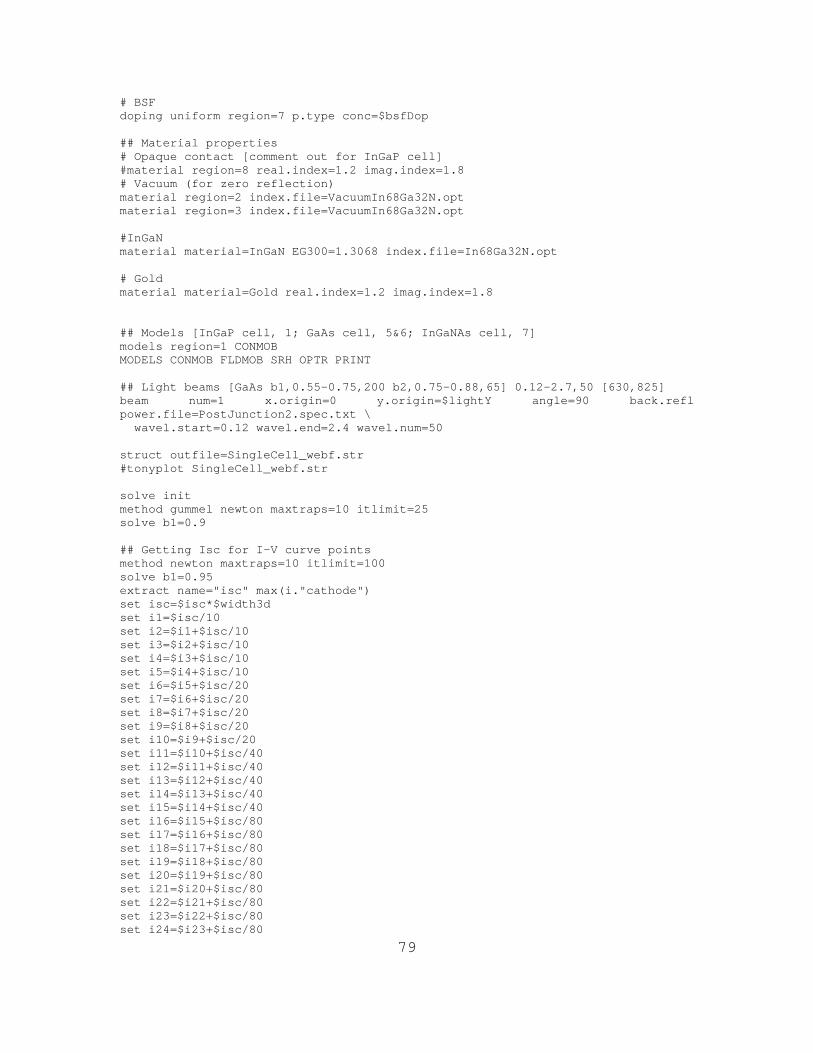
79
# BSF doping uniform region=7 p.type conc=$bsfDop ## Material properties # Opaque contact [comment out for InGaP cell] #material region=8 real.index=1.2 imag.index=1.8 # Vacuum (for zero reflection) material region=2 index.file=VacuumIn68Ga32N.opt material region=3 index.file=VacuumIn68Ga32N.opt #InGaN material material=InGaN EG300=1.3068 index.file=In68Ga32N.opt # Gold material material=Gold real.index=1.2 imag.index=1.8 ## Models [InGaP cell, 1; GaAs cell, 5&6; InGaNAs cell, 7] models region=1 CONMOB MODELS CONMOB FLDMOB SRH OPTR PRINT ## Light beams [GaAs b1,0.55-0.75,200 b2,0.75-0.88,65] 0.12-2.7,50 [630,825] beam num=1 x.origin=0 y.origin=$lightY angle=90 back.refl power.file=PostJunction2.spec.txt \ wavel.start=0.12 wavel.end=2.4 wavel.num=50 struct outfile=SingleCell_webf.str #tonyplot SingleCell_webf.str solve init method gummel newton maxtraps=10 itlimit=25 solve b1=0.9 ## Getting Isc for I-V curve points method newton maxtraps=10 itlimit=100 solve b1=0.95 extract name="isc" max(i."cathode") set isc=$isc*$width3d set i1=$isc/10 set i2=$i1+$isc/10 set i3=$i2+$isc/10 set i4=$i3+$isc/10 set i5=$i4+$isc/10 set i6=$i5+$isc/20 set i7=$i6+$isc/20 set i8=$i7+$isc/20 set i9=$i8+$isc/20 set i10=$i9+$isc/20 set i11=$i10+$isc/40 set i12=$i11+$isc/40 set i13=$i12+$isc/40 set i14=$i13+$isc/40 set i15=$i14+$isc/40 set i16=$i15+$isc/80 set i17=$i16+$isc/80 set i18=$i17+$isc/80 set i19=$i18+$isc/80 set i20=$i19+$isc/80 set i21=$i20+$isc/80 set i22=$i21+$isc/80 set i23=$i22+$isc/80 set i24=$i23+$isc/80

80
set i25=$i24+$isc/80-0.00001 ## log outfile=In68Ga32N.log method newton maxtraps=10 itlimit=100 solve b1=0.95 contact name=anode current method newton maxtraps=10 itlimit=100 ## Pmax points [InGaP 18-25; GaAs 15-25; InGaNAs 13-25; Ge 11-25] solve ianode=-$i25 b1=0.95 solve ianode=-$i24 b1=0.95 solve ianode=-$i23 b1=0.95 solve ianode=-$i22 b1=0.95 solve ianode=-$i21 b1=0.95 solve ianode=-$i20 b1=0.95 solve ianode=-$i19 b1=0.95 solve ianode=-$i18 b1=0.95 solve ianode=-$i17 b1=0.95 solve ianode=-$i16 b1=0.95 solve ianode=-$i15 b1=0.95 solve ianode=-$i14 b1=0.95 solve ianode=-$i13 b1=0.95 solve ianode=-$i12 b1=0.95 solve ianode=-$i11 b1=0.95 solve ianode=-$i10 b1=0.95 solve ianode=-$i9 b1=0.95 solve ianode=-$i8 b1=0.95 solve ianode=-$i7 b1=0.95 solve ianode=-$i6 b1=0.95 solve ianode=-$i5 b1=0.95 solve ianode=-$i4 b1=0.95 solve ianode=-$i3 b1=0.95 solve ianode=-$i2 b1=0.95 solve ianode=-$i1 b1=0.95 ## solve ianode=0 b1=0.95 log off extract name="iv" curve(v."anode", i."cathode") outfile="IVcurveIn68Ga32N.dat" tonyplot IVcurveIn68Ga32N.dat log outfile=doneIn68Ga32N.log log off
D. BOTTOM JUNCTION: IN0.78GA0.22N, EG=1.11 EV
go atlas set cellWidth=5.000000e+002 set capWidthpercent=8.000000e+000 set divs=1.000000e+001 set contThick=1.000000e-001 set capThick=3.000000e-001 set capDop=1.000000e+020

81
set windowThick=0.01 set winDop=2.15e17 set emitterThick=0.01 #changed emitDop from 1e16 to 1e20 set emitDop=1e16 set baseThick=3.19467 #changed basDop from 1e16 to 1e20 set baseDop=1e16 set bsfThick=0.03533 set bsfDop=2.15e19 set cellWidthDiv=$cellWidth/$divs set width3d=100e6/$cellWidth set capWidth=0.01*$capWidthpercent*$cellWidth/2 set capWidthDiv=$capWidth/($divs/2) set cellWidthHalf=$cellWidth/2 set bsfLo=0 set bsfHi=$bsfLo-$bsfThick set bsfDiv=$bsfThick/$divs set baseLo=$bsfHi set baseHi=$baseLo-$baseThick set baseMid=$baseLo-$baseThick/2 set baseDiv=$baseThick/$divs set emitterLo=$baseHi set emitterHi=$emitterLo-$emitterThick set emitterDiv=$emitterThick/$divs set windowLo=$emitterHi set windowHi=$windowLo-$windowThick set windowDiv=$windowThick/$divs set capLo=$windowHi set capHi=$capLo-$capThick #set capDiv=$capThick/$divs set contLo=$capHi set contHi=$contLo-$contThick set contDiv=$contThick/$divs set lightY=$emitterHi-5 mesh width=$width3d ## X-Mesh x.mesh loc=-$cellWidthHalf spac=$cellWidthDiv x.mesh loc=-$capWidth spac=$capWidthDiv x.mesh loc=$capWidth spac=$capWidthDiv x.mesh loc=$cellWidthHalf spac=$cellWidthDiv ## Y-Mesh # Top contact y.mesh loc=$contHi spac=0 y.mesh loc=$contLo spac=0 # Cap # Window y.mesh loc=$windowHi spac=$windowDiv y.mesh loc=$windowLo spac=$windowDiv # Emitter y.mesh loc=$emitterLo spac=$emitterDiv # Base

82
y.mesh loc=$baseMid spac=$baseDiv # BSF y.mesh loc=$bsfHi spac=$bsfDiv y.mesh loc=$bsfLo spac=$bsfDiv ## Regions # Cap #region num=8 material=Vacuum x.min=-$capWidth x.max=$capWidth y.min=$contHi y.max=$contLo region num=1 material=InGaN x.min=-$capWidth x.max=$capWidth y.min=$capHi y.max=$capLo x.comp=0.78 region num=2 material=Vacuum x.min=-$cellWidthHalf x.max=-$capWidth y.min=$contHi y.max=$capLo region num=3 material=Vacuum x.min=$capWidth x.max=$cellWidthHalf y.min=$contHi y.max=$capLo # Window [for Ge cell, use AlGaAs with x.comp=0.2] region num=4 material=InGaN x.min=-$cellWidthHalf x.max=$cellWidthHalf y.min=$windowHi y.max=$windowLo x.comp=0.78 #region num=4 material=AlGaAs x.comp=0.2 x.min=-$cellWidthHalf x.max=$cellWidthHalf y.min=$windowHi y.max=$windowLo # Emitter region num=5 material=InGaN x.min=-$cellWidthHalf x.max=$cellWidthHalf y.min=$emitterHi y.max=$emitterLo x.comp=0.78 # Base region num=6 material=InGaN x.min=-$cellWidthHalf x.max=$cellWidthHalf y.min=$baseHi y.max=$baseLo x.comp=0.78 # BSF region num=7 material=InGaN x.min=-$cellWidthHalf x.max=$cellWidthHalf y.min=$bsfHi y.max=$bsfLo x.comp=0.78 ## Electrodes [for InGaP cell, add cathode (gold) and remove cathode (conductor)] electrode name=cathode material=Gold x.min=-$capWidth x.max=$capWidth y.min=$contHi y.max=$contLo #electrode name=cathode x.min=-$cellWidthHalf x.max=$cellWidthHalf y.min=$windowHi y.max=$windowHi electrode name=anode x.min=-$cellWidthHalf x.max=$cellWidthHalf y.min=$bsfLo y.max=$bsfLo ## Doping [for InGaP cell, uncomment cap doping] # Cap doping uniform region=1 n.type conc=$capDop # Window doping uniform region=4 n.type conc=$winDop # Emitter doping uniform region=5 n.type conc=$emitDop # Base doping uniform region=6 p.type conc=$baseDop # BSF doping uniform region=7 p.type conc=$bsfDop ## Material properties # Opaque contact [comment out for InGaP cell] #material region=8 real.index=1.2 imag.index=1.8 # Vacuum (for zero reflection) material region=2 index.file=VacuumInGa22N.opt material region=3 index.file=VacuumInGa22N.opt #InGaN material material=InGaN EG300=1.1076 index.file=InGa22N.opt

83
# Gold material material=Gold real.index=1.2 imag.index=1.8 ## Models [InGaP cell, 1; GaAs cell, 5&6; InGaNAs cell, 7] models region=1 CONMOB MODELS CONMOB FLDMOB SRH OPTR PRINT ## Light beams [GaAs b1,0.55-0.75,200 b2,0.75-0.88,65] 0.12-2.7,50 [630,825] beam num=1 x.origin=0 y.origin=$lightY angle=90 back.refl power.file=PostJunction3.spec.txt \ wavel.start=0.12 wavel.end=2.4 wavel.num=50 struct outfile=SingleCell_webf.str #tonyplot SingleCell_webf.str solve init method gummel newton maxtraps=10 itlimit=25 solve b1=0.9 ## Getting Isc for I-V curve points method newton maxtraps=10 itlimit=100 solve b1=0.95 extract name="isc" max(i."cathode") set isc=$isc*$width3d set i1=$isc/10 set i2=$i1+$isc/10 set i3=$i2+$isc/10 set i4=$i3+$isc/10 set i5=$i4+$isc/10 set i6=$i5+$isc/20 set i7=$i6+$isc/20 set i8=$i7+$isc/20 set i9=$i8+$isc/20 set i10=$i9+$isc/20 set i11=$i10+$isc/40 set i12=$i11+$isc/40 set i13=$i12+$isc/40 set i14=$i13+$isc/40 set i15=$i14+$isc/40 set i16=$i15+$isc/80 set i17=$i16+$isc/80 set i18=$i17+$isc/80 set i19=$i18+$isc/80 set i20=$i19+$isc/80 set i21=$i20+$isc/80 set i22=$i21+$isc/80 set i23=$i22+$isc/80 set i24=$i23+$isc/80 set i25=$i24+$isc/80-0.00001 ## log outfile=In78Ga22N.log method newton maxtraps=10 itlimit=100 solve b1=0.95 contact name=anode current method newton maxtraps=10 itlimit=100 ## Pmax points [InGaP 18-25; GaAs 15-25; InGaNAs 13-25; Ge 11-25]

84
solve ianode=-$i25 b1=0.95 solve ianode=-$i24 b1=0.95 solve ianode=-$i23 b1=0.95 solve ianode=-$i22 b1=0.95 solve ianode=-$i21 b1=0.95 solve ianode=-$i20 b1=0.95 solve ianode=-$i19 b1=0.95 solve ianode=-$i18 b1=0.95 solve ianode=-$i17 b1=0.95 solve ianode=-$i16 b1=0.95 solve ianode=-$i15 b1=0.95 solve ianode=-$i14 b1=0.95 solve ianode=-$i13 b1=0.95 solve ianode=-$i12 b1=0.95 solve ianode=-$i11 b1=0.95 solve ianode=-$i10 b1=0.95 solve ianode=-$i9 b1=0.95 solve ianode=-$i8 b1=0.95 solve ianode=-$i7 b1=0.95 solve ianode=-$i6 b1=0.95 solve ianode=-$i5 b1=0.95 solve ianode=-$i4 b1=0.95 solve ianode=-$i3 b1=0.95 solve ianode=-$i2 b1=0.95 solve ianode=-$i1 b1=0.95 ## solve ianode=0 b1=0.95 log off extract name="iv" curve(v."anode", i."cathode") outfile="IVcurveIn78Ga22N.dat" tonyplot IVcurveIn78Ga22N.dat log outfile=doneIn78Ga22N.log
log off

85
APPENDIX B: MATLAB CODE
The Matlab code provided in this appendix provided
auxiliary support in the interpretation and display Sivaco
Atlas log files.
Original code for some of the Matlab functions and
scripts was obtained from Michalopolous [1], Bates, [2],
Green [3], and Canfield [4]. Modifications to the code were
made to support this thesis.
A. INDIUM GALLIUM NITRIDE BAND GAP CALCULATIONS
%InGaN Bandgap calculations %Baldomero Garcia clc; %Constants EgGaN=3.42; EgInN=0.77; b=1.43; x=[0:0.0001:1]; % x=.67; % InConcentration=x % GaConcentration=1-x %Formula for finding EgInGaN EgInGaN=((1-x).*EgGaN)+(x.*EgInN)-(b.*x.*(1-x)) %Formula for finding x solve('(((1-x)*EgGaN)+(x*EgInN)-(b*x*(1-x)))-EgInGaN','x'); % The other EgInGaN that we're solving for is EgInGaN=1.1 % EgInGaN=2.095 % Gacomp=1-(1/2/b*(EgGaN-EgInN+b-(EgGaN^2-2*EgInN*EgGaN-2*b*EgGaN+EgInN^2-2*EgInN*b+b^2+4*b*EgInGaN)^(1/2))) % Incomp=(1/2/b*(EgGaN-EgInN+b-(EgGaN^2-2*EgInN*EgGaN-2*b*EgGaN+EgInN^2-2*EgInN*b+b^2+4*b*EgInGaN)^(1/2))) %Plot plot(x,EgInGaN,'b'); xlabel('Indium concentration (unitless ratio)'); ylabel('InGaN Band Gap (eV)'); title('Indium concentration vs InGaN Band Gap');

86
B. CONVERSION FROM DIELECTRIC CONSTANTS (EPSILONS) TO REFRACTION COEFFICIENTS (N, K)
Optical data needed to be provided n-k format. Some of
the data obtained was available in epsilon form. Therefore,
a conversion needed to be made. Michalopoulos generated the
function below [1].
% E2NK Convert the e1, e2 pairs into n, k pairs. % [n k] = E2NK(e1, e2) % (c)2001 by P. Michalopoulos function [n,k] = e2nk(e1, e2) ap = (e1 + sqrt(e1.^2 + e2.^2)) / 2; an = (e1 - sqrt(e1.^2 + e2.^2)) / 2; app = ap >= 0; anp = an >= 0; err = (app < 0) & (anp < 0); err = sum(err); if err ~= 0 disp('ERROR!') end a = ap .* app + an .* anp; n = sqrt(a); k = e2 ./ (2 * n);
C. CONVERSION FROM PHOTON ENERGY (EV) TO WAVELENGTH (UM)
Data was found in photon energy and wavelength form.
In order to make comparisons, conversion from one form to
another was necessary. Functions by Michalopoulos [1] are
given below.
% EV2UM Converts photon energy (eV) into wavelength (um). % (c)2001 by P. Michalopoulos function um = ev2um(ev)

87
h = 6.6260755e-34; eV = 1.60218e-19; c = 2.99792458e8; ev = ev * eV; f = ev / h; wavel = c ./ f; um = wavel / 1e-6;
% UM2EV Converts photon wavelength (um) into energy (eV). % (c)2001 by P. Michalopoulos function ev = um2ev(um) h = 6.6260755e-34; eV = 1.60218e-19; c = 2.99792458e8; wavel = um * 1e-6; f = c ./ wavel; ev = h * f; ev = ev ./ eV;
D. IV CURVE PLOTS FOR INDIUM GALLIUM NITRIDE QUAD JUNCTION SOLAR CELL
% Code modified from Canfield's source code % Data obtained from log files from InGaN quad-junction solar cell % Baldomero Garcia clc; % In20Ga80N with AM0 spectrum current1=[0.0176131398 0.0176031407 0.0175505986 0.0174980573 0.0173929742 0.0171728094 0.0169526469 0.0167324843 0.0165123158 0.0162921532 0.0160719881 0.0158518253 0.0156316602 0.0154114983 0.0149711686 0.0145308402 0.0140905121 0.0136501825 0.0132098541 0.0123291993 0.0114485415 0.0105678837 0.0096872266 0.0088065691 0.0070452558 0.0052839419 0.0035226276 0.0017613142 -0.0000000001]; voltage1=[0.0000000000 0.2970913579 1.1822462140 1.5075176680 1.7472436590 1.8900757790 1.9378145180 1.9663764170 1.9875670060 2.0047710060 2.0194136280 2.0322369610 2.0436835120 2.0540360290 2.0722008890 2.0877645130 2.1013319790 2.1132957310 2.1239292560 2.1419700890 2.1566166780 2.1686629450 2.1786938920 2.1871519430 2.2006132650 2.2108811030 2.2190289820 2.2257052930 2.2313181110]; % In57Ga43N with postjunction1 spectrum

88
current2=[0.0171128720 0.0171028783 0.0168989671 0.0166850573 0.0164711457 0.0162572338 0.0160433258 0.0158294126 0.0156155026 0.0154015923 0.0151876797 0.0149737698 0.0145459485 0.0141181240 0.0136903032 0.0132624807 0.0128346588 0.0119790166 0.0111233713 0.0102677280 0.0094120828 0.0085564398 0.0068451513 0.0051338641 0.0034225761 0.0017112879 -0.0000000001]; voltage2=[0.0000000000 0.1305081858 0.8192581792 0.9015131674 0.9331338594 0.9534997163 0.9689573887 0.9815965012 0.9923675261 1.0017892410 1.0101786220 1.0177449700 1.0309568480 1.0422028240 1.0519502020 1.0605082500 1.0680958050 1.0809744750 1.0915085520 1.1002972060 1.1077533400 1.1141715070 1.1247003520 1.1330384420 1.1398643710 1.1456000250 1.1505207070]; % In68Ga32N with postjunction2 spectrum current3=[0.0141231105 0.0141131184 0.0140298496 0.0139465807 0.0137700408 0.0135935022 0.0134169620 0.0132404230 0.0130638854 0.0128873465 0.0127108077 0.0125342689 0.0123577303 0.0120046521 0.0116515739 0.0112984952 0.0109454185 0.0105923395 0.0098861822 0.0091800273 0.0084738721 0.0077677158 0.0070615601 0.0056492474 0.0042369367 0.0028246240 0.0014123119 0.0000000001]; voltage3=[0.0000000000 0.1311096030 0.5441673681 0.6320277025 0.6842499725 0.7083967768 0.7248954021 0.7377135412 0.7483143199 0.7574074704 0.7653951663 0.7725296065 0.7789805527 0.7902824668 0.7999460470 0.8083630634 0.8157932979 0.8224203640 0.8337763994 0.8431914560 0.8511524069 0.8579918718 0.8639469242 0.8738573284 0.8818299562 0.8884345077 0.8940340114 0.8988707325]; % In78Ga22N with potjunction3 spectrum current4=[0.0128841840 0.0128741794 0.0127231275 0.0125620760 0.0124010228 0.0122399704 0.0120789198 0.0119178658 0.0117568129 0.0115957622 0.0114347108 0.0112736577 0.0109515531 0.0106294488 0.0103073439 0.0099852400 0.0096631342 0.0090189240 0.0083747191 0.0077305090 0.0070862990 0.0064420895 0.0051536706 0.0038652545 0.0025768364 0.0012884183 -0.0000000001]; voltage4=[0.0000000000 0.1078032006 0.4688474643 0.5100668879 0.5309258388 0.5454971566 0.5569116230 0.5663876299 0.5745324881 0.5816962863 0.5881009992 0.5938970077 0.6040640671 0.6127739225 0.6203776540 0.6271079482 0.6331288820 0.6434973415 0.6521554853 0.6595301586 0.6659109540 0.6715037308 0.6808929507 0.6885228391 0.6948948317 0.7003322584 0.7050534598]; % Combined current5=[0 0.001991 0.004011 0.006003 0.007994 0.01001 0.01178 0.01198 0.0126 0.01275 0.01286 0.0128841840]; voltage5=[4.9793 4.9542 4.9195 4.8744 4.8185 4.7271 4.5995 4.5723 4.4736 4.3906 4.0906 0]; P1=current1.*voltage1; [a b]=max(P1);

89
Pmax1=voltage1(b)*current1(b); Voc1=max(voltage1); Isc1=max(current1); FF1=Pmax1/(Voc1*Isc1) Eff1=100*Pmax1/(.1353) P2=current2.*voltage2; [c d]=max(P2); Pmax2=voltage2(d)*current2(d); Voc2=max(voltage2); Isc2=max(current2); FF2=Pmax2/(Voc2*Isc2) Eff2=100*Pmax2/(.1353) P3=current3.*voltage3; [e f]=max(P3); Pmax3=voltage3(f)*current3(f); Voc3=max(voltage3); Isc3=max(current3); FF3=Pmax3/(Voc3*Isc3) Eff3=100*Pmax3/(.1353) P4=current4.*voltage4; [g h]=max(P4); Pmax4=voltage4(h)*current4(h); Voc4=max(voltage4); Isc4=max(current4); FF4=Pmax4/(Voc4*Isc4) Eff4=100*Pmax4/(.1353) P5=current5.*voltage5; [k l]=max(P5); Pmax5=voltage5(l)*current5(l); Voc5=max(voltage5); Isc5=max(current5); FF5=Pmax5/(Voc5*Isc5) Eff5=100*Pmax5/(.1353) plot(voltage1,current1,'r'); %grid on; hold on; %plot(voltage1(b),current1(b),'o'); hold on; plot(voltage2,current2,'r'); hold on; %plot(voltage2(d),current2(d),'o'); hold on; plot(voltage3,current3,'r'); hold on; %plot(voltage3(f),current3(f),'o'); hold on; plot(voltage4,current4,'r'); hold on; %plot(voltage4(h),current4(h),'o'); hold on;

90
plot(voltage5,current5,'b'); hold on; plot(voltage5(l),current5(l),'or'); hold off; xlabel('Voltage (V)') ylabel('Current Density (A/cm^2)') title('Solar Cell IV Curve') axis([0 5.5 0 0.020])
E. AIR MASS ZERO PLOTS
Air Mass Zero (AM0) data was obtained from NREL [19]
and plotted using the Matlab function provided by
Michalopoulos [1]. It was modified to provide an additional
plot.
% AMSPECTRUMS Plot the data contained in spectrums.mat % Check the source code and uncomment the required lines. % (c)2001 by P. Michalopoulos h = 6.6260755e-34; eV = 1.60218e-19; c = 2.99792458e8; load('Data\spectrums') plot(AM0_wavel, AM0_int1, 'b', AM15a_wavel, AM15a_int1, 'r'), grid on title('AM 0 and AM 1.5 spectra'), xlabel('Wavelength [um]'), ylabel('Irradiance [W / cm^2*um]') axis([0 3 0 0.23])
The code above was modified to display AM0 with respect
to photon energy and wavelength, respectively.
Figure (1) plot(um,iradiance,'r'); xlabel('Wavelength (um)') ylabel('Irradiance W/cm^2*um') title('AM0') axis([0 2.5 0 0.25]) Figure (2) plot(ev,iradiance,'b'); xlabel('Energy (eV)') ylabel('Irradiance W/cm^2um') title('AM0') axis([0 6.0 0 0.25])

91
LIST OF REFERENCES
[1] P. Michalopoulous, “A novel approach for the development and optimization of state-of-the-art photovoltaic devices using Silvaco”, Master’s Thesis, Naval Postgraduate School, Monterey, California, 2002.
[2] A. D. Bates, “Novel optimization techniques for multijunction solar cell design using Silvaco Atlas”, Master’s Thesis, Naval Postgraduate School, Monterey, California, 2004.
[3] M. Green, “The verification of Silvaco as a solar cell simulation tool and the design and optimization of a four-junction solar cell”, Master’s Thesis, Naval Postgraduate School, Monterey, California, 2003.
[4] B. J. Canfield, “Advanced modeling of high temperature performance of Indium Gallium Arsenide thermophotovoltaic cells”, Master’s Thesis, Naval Postgraduate School, Monterey, California, 2005.
[5] A. S. Bouazzi, H. Hamzaoui, B. Rezig, “Theoretical possibilities of InGaN tandem PV structures”, Solar Energy Materials & Solar Cells, Vol. 87, 595-603, 2004.
[6] S. M. Sze, Semiconductor Devices, 2nd edition, John Wiley & Sons, Inc, 2001.
[7] Periodic table of elements, 21 March 2007, http://www.nrc-cnrc.gc.ca/student-science-tech/.
[8] Silicon atomic structure, 13 March 2007, http://www.micromountain.com/sci_diagrams/at_struct/at_struct_pages/silicon_lab_none.htm.
[9] R. F. Pierret, Semiconductor Device Fundamentals, Addison-Wesley Publishing, Reading, Massachusetts, 1996.
[10] J. Nelson, The Physics of Solar Cells, Imperial College Press, London, England, 2003.
[11] Indium Nitride and Gallium Nitride atoms per cm3, 2 May 2007, http://www.ioffe.rssi.ru/SVA/NSM/Semicond/index.html.

92
[12] S. S. Hegedus and A. Luque, “Status, trends, challenges and the bright future of solar electricity from photovoltaics”, in Handbook of Photovoltaic Science and Engineering, Luque, A. and Hegedus S.S., eds, p. 12, John Wiley & Sons, 2003.
[13] Light spectrum, 2 May 2007, http://www1.eere.energy.gov/solar/pv_cell_light.html.
[14] Color wavelength table, 2 May 2007, http://www.usbyte.com/common/approximate_wavelength.htm.
[15] Light energy absorption with respect to band gap, 2 May 2007, http://www1.eere.energy.gov/solar/bandgap_energies.html.
[16] Simple cubic lattice structure, 24 April 2007, http://upload.wikimedia.org/wikipedia/commons/thumb/5/55/Cubic.svg/109px-Cubic.svg.png.
[17] I. Vurgaftman, J. R. Meyer, L. R. Ram–Mohan, “Band parameters for III–V compound semiconductors and their alloys”, Applied Physics Review, Journal of Applied Physics, Vol. 89, number 11, pp. 5815–5875, 2001.
[18] I. Vurgaftman and J. R. Meyer, “Band parameters for
nitrogen-containing semiconductors”, Journal of Applied Physics, Volume No. 6, Number 6, pp. 3675-3696, 2003.
[19] National Renewable Energy (NREL) Air Mass Zero (AM0)
solar spectrum, 17 April 2007, http://rredc.nrel.gov/solar/spectra/am0/.
[20] J. L. Gray, “The physics of the solar cell”, in
Handbook of Photovoltaic Science and Engineering, A. Luque and S.S. Hegedus, eds, p. 12, John Wiley & Sons, 2003.
[21] F. Lasnier and T. G. Ang, Photovoltaic Engineering
Handbook, Adam Hilger, Bristol, UK, 1990. [22] Silvaco International, 8 May 2007,
http://www.silvaco.com/products/device_simulation/atlas.html.
[23] Atlas User’s Manual, Silvaco International, 2005.

93
[24] V. Y. Davydov, et al., “Absorption and emission of hexagonal InN. Evidence of narrow fundamental band gap”, Phys. Stat. Sol. (b) 229, No. 3, R1-R3, 2002.
[25] V. Y. Davydov, et al., “Band gap of InN and In-Rich InxGa1-xN alloys (0.36<x<1)”, Phys. Stat. Sol. (b) 230, No. 2, R4–R6, 2002.
[26] Spectrum and InGaN band gaps, 8 May 2007, http://emat-solar.lbl.gov/images/InGaN_Solar.gif.
[27] P. Specht, et al., “Band transitions in wurtzite GaN and InN determined by valence electron energy loss spectroscopy”, Solid State Communications 135, 340–344, 2005.
[28] W. Walukiewicz, “Native defects in InGaN alloys”, Physica B, 376-377, 432-435, 2006.
[29] W. Walukiewicz, “Narrow band gap group III-nitride alloys”, Physica E 20, 300 – 307, 2004.
[30] J. Wu, et al., “Small band gap bowing in InGaN alloys”, Applied Physics Letters, Volume 80, Number 25, 4741-4743, 2002.
[31] J. W. Ager III and W. Walukiewicz, “High efficiency, radiation-hard solar cells”, Lawrence Berkeley National Laboratory, Paper LBNL 56326, 2004.
[32] J. Wu and W. Walukiewicz, “Band gaps of InN and group III nitride alloys”, Superlattices and Microstructures, 34, 63–75, 2003.
[33] R. E. Jones, et al., “Evidence for p-type doping of InN”, Lawrence Berkeley National Laboratory, Paper LBNL 59255, 2005.
[34] P. Specht and C. Kisielowski, Dielectric constants for In0.20Ga0.80N, unpublished, 2006.
[35] R. Goldhahn, et al., “Dielectric function of “narrow” band gap InN”, Mat. Res. Soc. Symp. Proc. Vol. 743, L5.9.1-L5.9.6, 2003.
[36] R. R. King, et al., “Advanced III-V Multijunction Cells for space”, Spectrolab Inc, Sylmar, California, 2006.

94
[37] F. Bechstedt, et al., “Energy gap and optical properties of InxGa1-xN”, Phys. Stat. Sol. (a) 195, No. 3, pp. 628-633, 2003.

95
INITIAL DISTRIBUTION LIST
1. Defense Technical Information Center Ft. Belvoir, Virginia
2. Dudley Knox Library Naval Postgraduate School Monterey, California
3. Sherif Michael Naval Postgraduate School Monterey, California
4. Todd Weatherford Naval Postgraduate School Monterey, California
5. Wladek Walukiewicz Lawrence Berkeley National Laboratory Berkeley, California
6. Petra Specht Lawrence Berkeley National Laboratory Berkeley, California