Increased Pulse Rep. Rates for Solid State Thyratron ... Power... · Increased Pulse Rep. Rates for...
15
Increased Pulse Rep. Rates for Solid State Thyratron Replacements John Waldron Silicon Power Corporation 280 Great Valley Pkwy Malvern, PA 19355 PPPS 2019 Orlando, FL 23-282 June, 2019 [email protected]
Transcript of Increased Pulse Rep. Rates for Solid State Thyratron ... Power... · Increased Pulse Rep. Rates for...

Increased Pulse Rep. Rates for Solid State Thyratron Replacements
John WaldronSilicon Power Corporation280 Great Valley PkwyMalvern, PA 19355
PPPS 2019 Orlando, FL 23-282 June, [email protected]
PPPS 2019 Orlando, FL 23-282 June, [email protected]
Outline
• Introduction to Solidtron’s Enabling Technology– Pulse discharge targeted designs
• Solidtron Performance– Discharge Performance
– Increased Pulse Repetition Rate Strategy/Results
• Solid State Discharge Switch Replacements – Motivation
– Approach
– Experimental results
• Summary
• Questions
2

PPPS 2019 Orlando, FL 23-282 June, [email protected]
160,000 cells/cm2
SGTO
GTO
~ 50 cells /cm2
SGTO Advantages:
Cell structure 3000 x denser
Upper transistor >100x improved
• Forward drop greatly reduced
• Three times lower turn-off switching loss
Die sizes from 3x3mm to 15x22mm in 200mm IC foundry providing very high yield, repeatability and uniformity!
3
Super-GTO Vs. GTOSGTO is an IC foundry-fabricated GTO mated with Silicon Power’s proprietary low inductance ThinPak package
• Turn-on improved by 2 orders of magnitude
PPPS 2019 Orlando, FL 23-282 June, [email protected] 4
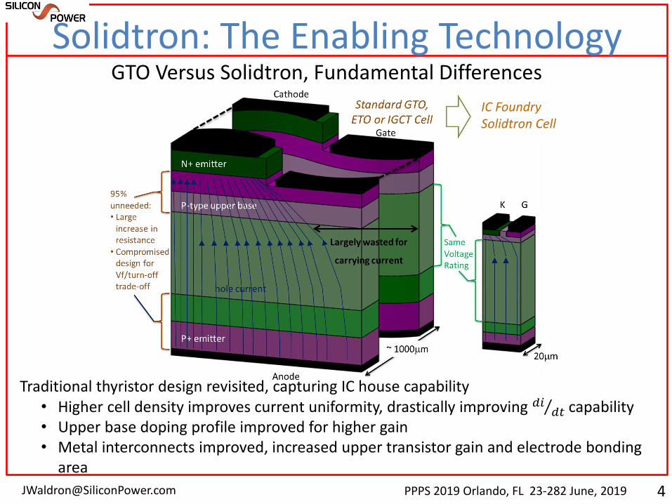
Solidtron: The Enabling Technology
Traditional thyristor design revisited, capturing IC house capability• Higher cell density improves current uniformity, drastically improving Τ𝑑𝑖
𝑑𝑡 capability• Upper base doping profile improved for higher gain • Metal interconnects improved, increased upper transistor gain and electrode bonding
area
IC Foundry Solidtron Cell
GTO Versus Solidtron, Fundamental Differences

PPPS 2019 Orlando, FL 23-282 June, [email protected]
Solidtron Advantages
• Cell density further enhanced
• Emitter area maximized
• Internal metal interconnect density improved
• Upper transistor gain further improved
• Increased cathode bonding pad area
8 inch starting material and improved manufacturing process further improving yield while driving cost down
5
Solidtron Vs. Super-GTOSolidtron follows SGTO strategy, focusing on pulse discharge versus turn-off applications
PPPS 2019 Orlando, FL 23-282 June, [email protected]
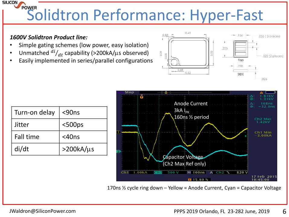
1600V Solidtron Product line:• Simple gating schemes (low power, easy isolation)• Unmatched Τ𝑑𝑖
𝑑𝑡 capability (>200kA/ms observed)• Easily implemented in series/parallel configurations
6
Solidtron Performance: Hyper-Fast
Capacitor Voltage (Ch2 Max Ref only)
Anode Current 3kA IPK
160ns ½ period
170ns ½ cycle ring down – Yellow = Anode Current, Cyan = Capacitor Voltage
Turn-on delay <90ns
Jitter <500ps
Fall time <40ns
di/dt >200kA/ms
PPPS 2019 Orlando, FL 23-282 June, [email protected]
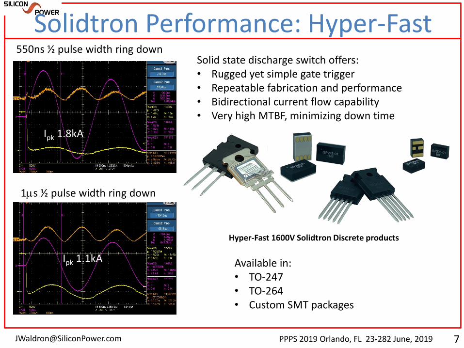
Solidtron Performance: Hyper-Fast
7
550ns ½ pulse width ring down
1ms ½ pulse width ring down
Solid state discharge switch offers:• Rugged yet simple gate trigger• Repeatable fabrication and performance• Bidirectional current flow capability• Very high MTBF, minimizing down time
Ipk 1.8kA
Ipk 1.1kA
Hyper-Fast 1600V Solidtron Discrete products
Available in:• TO-247 • TO-264• Custom SMT packages

PPPS 2019 Orlando, FL 23-282 June, [email protected] 8
Solidtron: Increased Switching Speed
Punch-through design:• Higher BV for given device thickness• Allows bipolar current conduction• Improves turn-on speed• Reduces commutation time
Lower-base width and doping concentration determines BV

PPPS 2019 Orlando, FL 23-282 June, [email protected] 9
Solidtron: Increased Switching Speed
One factor contributing to commutation time is stored charge remaining in lower-base• Thinner lower-base results in less stored charge • Thinner lower-base reduces distance required for diffused carrier to reach emitter
Physically narrower lower-base is employed
¼
Can be thinned after processing to reduce Ron
Implementing lower voltage devices improves commutation time
PPPS 2019 Orlando, FL 23-282 June, [email protected] 10
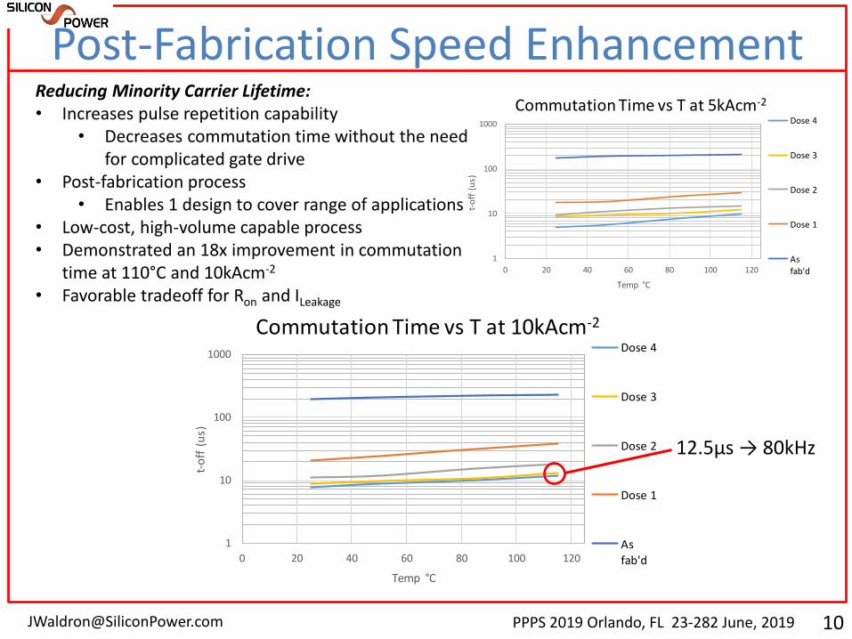
Post-Fabrication Speed Enhancement
1
10
100
1000
0 20 40 60 80 100 120
t-o
ff (
us)
Temp °C
Commutation Time vs T at 5kAcm-2
Dose 4
Dose 3
Dose 2
Dose 1
As
fab'd
1
10
100
1000
0 20 40 60 80 100 120
t-o
ff (
us)
Temp °C
Commutation Time vs T at 10kAcm-2
Dose 4
Dose 3
Dose 2
Dose 1
As
fab'd
Reducing Minority Carrier Lifetime:• Increases pulse repetition capability
• Decreases commutation time without the need for complicated gate drive
• Post-fabrication process• Enables 1 design to cover range of applications
• Low-cost, high-volume capable process• Demonstrated an 18x improvement in commutation
time at 110°C and 10kAcm-2
• Favorable tradeoff for Ron and ILeakage
12.5µs → 80kHz

PPPS 2019 Orlando, FL 23-282 June, [email protected] 11
Post-Fabrication Speed Enhancement
1.0E-02
1.0E-01
1.0E+00
1.0E+01
1.0E+02
0 1 2 3 4 5
Lea
kage
Cu
rren
t (µ
A)
Dose #
Leakage Current at 1500V
as fab'd 85°C as fab'd 110°C
1 85°C 2 85°C
1 110°C 2 110°C
3 85°C 3 110°C
4 85°C 4 110°C
0
0.5
1
1.5
2
2.5
3
3.5
4
4.5
5
200 400 600 800 1000 1200
R-o
n (
mO
hm
)
J (Acm-2)
Differential Resistance at 110°C Dose 4 Dose 3
Dose 2 Dose 1
As fab'd
Reducing Minority Carrier Lifetime Tradeoffs:• Lower base gain is reduced, ↑ RON
• Lower τ increases generation current (↑leakage)• However, small ↑RON (<2x) for almost 20x
improvement in pulse rep rate
0 1 2 3 4 5
Rel
ati
ve L
ifet
ime
(A.I
.)
Dose #
Relative Lifetime Vs Dose
PPPS 2019 Orlando, FL 23-282 June, [email protected] 12
Solid State Discharge SwitchesMotivation
• Compliance with RoHS • Eliminate conditioning requirements• Eliminate requisite heaters• Simplify gating
• Built in gating requires TTL/Optical trigger and DC power supply• Improve efficiency
• In both energy transfer and off-state conditions• Improve turn-on delay and jitter• Increase usable lifetime
• No terminal erosion• Eliminate liquid cooling requirements• Increase mechanical installation flexibility• Improved performance over IGBT/SCR-based solid state switch replacements

PPPS 2019 Orlando, FL 23-282 June, [email protected] 13
Hyper-Fast Solid State Thyratron Replacement40kV SSTR-1 (Twin Stack)• Initial TO-247 version demonstrated 365k pulses
o 3kA, 300ns square wave
• Similar 20kV and 60kV derivatives planned to complete the product offering
• Negligible power dissipation in off-state (snubber resistors much higher in value)
• TO-264 version offers up to 30x increase in action
TO-247: SP245-03TO-264: SP275-02

PPPS 2019 Orlando, FL 23-282 June, [email protected] 14
Solid State Thyratron Replacement
40kV SSTR-1 (Twin Stack) Vs. e2v CX2282
Hyper-Fast 1600V Solidtron
• Τ𝑑𝑖𝑑𝑡 capability is >200kA/mSec
• Fiber Optically Triggered
• Small size - 9” Tall, 3.75” Base diameter
• Voltage capability of 40kV
• Yellow - 4.7kA Peak Current w/average Τ𝑑𝑖
𝑑𝑡 of ~60kA/mSec(Circuit Limited)
• Magenta - 36kV Discharge
Anode Current
Capacitor Voltage (Ch2 Max Ref only)
50nSec rise timePeak I >4kARep Rate = 100PPS

PPPS 2019 Orlando, FL 23-282 June, [email protected]
Summary
15
• RoHS compliance
• Unparalleled solid state Τ𝑑𝑖𝑑𝑡 capabilities
– Hyper-fast demonstrated 200kA/ms
• 𝑓(𝑖 𝑡 , 𝜏) capability, determined by experimental and/or sim data exceeds most if not all commercially available gas or solid state thyratrons available
• Designed with modular, scalable sub-assemblies
– Enables fitment for most thyratron or ignitron applications