
In System Configuration - hercules-micro.com
16
In System Configuration App Notes Apr. 2020 Hercules Microelectronics Co., Ltd.
Transcript of In System Configuration - hercules-micro.com

In System Configuration
App Notes
Apr. 2020
Hercules Microelectronics Co., Ltd.

In System Configuration App Notes
http://www.hercules-micro.com 1
Notes
Copyright © 2020 Hercules
Microelectronics, Inc. All rights reserved.
No part of this document may be copied,
transmitted, transcribed, stored in a retrieval
system, or translated into any language or
computer language, in any form or by any
means, electronic, mechanical, magnetic,
optical, chemical, manual or otherwise,
without the written permission of Hercules
Microelectronics, Inc. All trademarks are the
property of their respective companies.
Version Number
HME-H1D03AN02-ISC
Contact Us
If you have any problems or requirements
during using our product, please contact
Hercules Microelectronics, Inc. or your
local distributors, or send e-mail to
Environmental Considerations
To avoid the harmful substances being
released into the environment or harming
human health, we encourage you to recycle
this product in an appropriate way to make
sure that most of the materials are reused or
recycled appropriately. Please contact your
local authorities for disposal or recycle
information.
Warranty
The information in this document has been
carefully checked and is believed to be entirely
reliable. However, no responsibility is assumed
for inaccuracies. Furthermore, Hercules
Microelectronics, Inc. reserves the right to
discontinue or make changes, without prior
notice, to any products herein to improve
reliability, function, or design.
Hercules Microelectronics, Inc. advises its
customers to obtain the latest version of the
relevant information to verify, before placing
orders, that the information being relied upon is
current.
The product introduced in this book is not
authorized for use as critical components in life
support devices or systems without the express
written approval of Hercules Microelectronics,
Inc. As used herein: 1. Life support devices or
systems are devices or systems that (a) are
intended for surgical implant into the body or (b)
support or sustain life, and whose failure to
perform, when properly used in accordance with
instructions for use provided in the labeling, can
be reasonably expected to result in a significant
injury to the user. 2. A critical component is any
component of a life support device or system
whose failure to perform can be reasonably
expected to cause the failure of the life support
device or system, or to affect its safety or
effectiveness.

In System Configuration App Notes
http://www.hercules-micro.com 2
Revision History
The table below shows the revision history for this document.
Date Version Revision
Apr. 2020 1.0 Initial release.

In System Configuration App Notes
http://www.hercules-micro.com 3
Table of Contents
In System Configuration Overview ................................................................................................. 4
Interface Description ........................................................................................................................ 5
PBUS Write ........................................................................................................................... 5
PBUS Read .......................................................................................................................... 6
ISC Register Description .................................................................................................................. 7
ISC Example ...................................................................................................................................... 8
FPGA Design ........................................................................................................................ 8
8051 Design ....................................................................................................................... 12
MCF Download ................................................................................................................................ 14

In System Configuration App Notes
http://www.hercules-micro.com 4
In System Configuration Overview
H1D03 family has the ISC (In System Configuration) feature which can make the application
reconfigure the H1D03 device dynamically or statically in the AS mode.
During the static reconfiguration, the application program writes addresses and instructions to
corresponding registers of ISC, which makes the H1D03 device reload corresponding image from a
certain SPI Flash address, thus realizing the reconfiguration.
During the dynamic reconfiguration, the application program reads the image from external (USART
or other interfaces), writes the image to corresponding image space through the SPI interface, and
updates the Image. Then the application writes addresses and instructions to corresponding
registers of ISC and configures the application with the updated image.
With the ISC feature, the H1D03 device can virtually expand the device volume by the SPI FLASH
space. In other words, H1D03 device can fulfill several applications if each of the images logic can
be implemented in the same H1D03’s board.
The configuration image of the H1D03 device consists of FPGA configuration data and 8051
programming code. The configuration image is stored in the SPI FLASH. Sector is the smallest unit
to store images. One image needs about 3 sectors. In addition, one image can take more than one
sectors. The following figure describes the mapping of multi-Images stored in the SPI FLASH, therein
the image size is smaller than three sectors.
The ISC’s function diagram is shown below.
0000000
0030000
ISCREG
H1D03 Device
SPI Interface
0060000
SPI-FLASH address
Image1bitstream
firmware
Image2bitstream
firmware
Image3bitstream
firmware
FP
Configuration
SOC_MASTER_BUS
Figure 1 Function Diagram of ISC

In System Configuration App Notes
http://www.hercules-micro.com 5
Interface Description The FP operates on the ISC register in the configuration block via the SOC_MASTER_BUS PBUS
interface to realize the ISC function.
Table 1 SOC_MASTER_BUS PBUS Interface
Signal Direction Description
fp_m_pbus_addr[7:0] output Pbus address
fp_m_pbus_write output 1: write ; 0: read
fp_m_pbus_wdata[15:0] output Write data
fp_m_pbus_req output Read/write request, high valid
fp_m_prdata[15:0] input Read data
fp_m_pbus_gnt input Bus read/write grant, high valid
PBUS Write
req
paddr A0
pwrite
gnt
clk
pwdata D0
Figure 2 Bus Write
The Master sets the address, writes data, sends the req to the slave, and keeps these signals until
the slave’s gnt signal becomes valid.

In System Configuration App Notes
http://www.hercules-micro.com 6
PBUS Read
Figure 3 Bus Read
The Master sets the address, sends the req to the slave, and keeps these signals until the slave’s
gnt signal becomes valid.

In System Configuration App Notes
http://www.hercules-micro.com 7
ISC Register Description
The RECFG_CTRL register which is used to control the ISC funciton is a 32b internal register. The
SOC_MASTER_BUS is a 16b bus. The SOC_MASTER_BUS needs two operations to access the
RECFG_CTRL register. The pwdata will be written to the 32b register until the SOC_MASTER_BUS
writes data to the 1 address. It is better for the SOC_MASTER_BUS to access the RECFG_CTRL
register in the order of 0 address and then 1 address.
Table 2 SOC_MASTER_BUS PBUS Address MAP
FPGA address Pbus address Register Description
0x0,0x1 4170_0160 0x0, access low 16bit; 0x1, access high 16bit.
Table 3 FP_RECFG_CTRL Register
Address: 0x4170_0160
Bits Name Type default Description
31 Fp_recfg_start RW 0 FPGA start reconfig, active high, self clear.
30:24 RO
23:0 As_source_addr RW 0
FPGA reconfig start address. The H1D03
device will load the image to configure the
device from the As_source_addr.

In System Configuration App Notes
http://www.hercules-micro.com 8
ISC Example
The following example describes that the 8051 program reconfigures the H1D03 device. The
example uses the FPGA logic design and 8051 program to implement the ISC function.
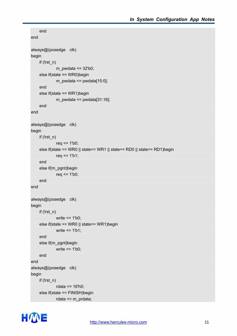
FPGA Design
The master_logic module generates two 16-bit operations to the SOC_MASTER_BUS by FSM when
the ‘start’ signal is valid. The detail rtl code is shown below.
Table 4 master_logic module signals
Signal Direction Description
clk input Module clock
rst_n input Reset signal, active low
start input Operation start signal, high active
done output Operation finish signal, high active
paddr[7:0] input SOC_MASTER_BUS address
pwrite input 1: write ; 0: read
pwdata[31:0] input Write data
prdata[31:0] output Read data
module master_logic(
clk ,
rst_n ,
start ,
paddr ,
pwdata ,
prdata ,
pwrite ,
done ,
);
input clk;
input rst_n;
input start;
input pwrite;
input [7:0]paddr;
input [31:0]pwdata;
output [31:0]prdata;
output done;

In System Configuration App Notes
http://www.hercules-micro.com 9
reg [7:0] m_paddr;
reg [15:0] m_pwdata;
wire m_pwrite;
wire [15:0] m_prdata;
wire m_pgnt;
wire pwrite_p,start_p;
reg req;
reg write;
reg done;
reg [31:0] rdata;
reg [9:0] state,n_state;
parameter
IDLE = 10'b0000000001,
WR0 = 10'b0000000010,
WGNT0 = 10'b0000000100,
WR1 = 10'b0000001000,
WGNT1 = 10'b0000010000,
RD0 = 10'b0000100000,
RGNT0 = 10'b0001000000,
RD1 = 10'b0010000000,
RGNT1 = 10'b0100000000,
FINISH = 10'b1000010000;
one_shot start_shot(
.sys_rst_l (rst_n),
.clk_in (clk),
.d (start),
.q (start_p)
);
always@(posedge clk)
begin
if(!rst_n)begin
state <= IDLE;
end
else
state <= n_state;
end
always@(state or start_p or pwrite or m_pgnt)

In System Configuration App Notes
http://www.hercules-micro.com 10
begin
case(state)
IDLE:
if (start_p) begin
if(pwrite)n_state <= WR0;
else n_state <= RD0;
end
else n_state <= IDLE;
WR0:
n_state <= WGNT0;
WGNT0:
if(m_pgnt)n_state <= WR1;
else n_state <= WGNT0;
WR1:
n_state <= WGNT1;
WGNT1:
if(m_pgnt)n_state <= FINISH;
else n_state <= WGNT1;
RD0:
n_state <= RGNT0;
RGNT0:
if(m_pgnt)n_state <= RD1;
else n_state <= RGNT0;
RD1:
n_state <= RGNT1;
RGNT1:
if(m_pgnt)n_state <= FINISH;
else n_state <= RGNT1;
FINISH:
n_state <= IDLE;
default:
n_state <= IDLE;
endcase
end
always@(posedge clk)
begin
if (!rst_n)
m_paddr <= 8'b0;
else if(state == WR0)begin
m_paddr <= {paddr[7:1],1'b0};
end
else if(state == WR1)begin
m_paddr <= {paddr[7:1],1'b1};
In System Configuration App Notes
http://www.hercules-micro.com 11
end
end
always@(posedge clk)
begin
if (!rst_n)
m_pwdata <= 32'b0;
else if(state == WR0)begin
m_pwdata <= pwdata[15:0];
end
else if(state == WR1)begin
m_pwdata <= pwdata[31:16];
end
end
always@(posedge clk)
begin
if (!rst_n)
req <= 1'b0;
else if(state == WR0 || state== WR1 || state== RD0 || state== RD1)begin
req <= 1'b1;
end
else if(m_pgnt)begin
req <= 1'b0;
end
end
always@(posedge clk)
begin
if (!rst_n)
write <= 1'b0;
else if(state == WR0 || state== WR1)begin
write <= 1'b1;
end
else if(m_pgnt)begin
write <= 1'b0;
end
end
always@(posedge clk)
begin
if (!rst_n)
rdata <= 16'h0;
else if(state == FINISH)begin
rdata <= m_prdata;

In System Configuration App Notes
http://www.hercules-micro.com 12
end
end
always@(posedge clk)
begin
if (!rst_n)
done <= 1'b0;
else if(state==FINISH)begin
done <= 1'b1;
end
else begin
done <= 1'b0;
end
end
SOC_MASTER_BUS u_master(
.fp_m_paddr (m_paddr[7:0] ),
.fp_m_preq (m_preq ),
.fp_m_pwdata (m_pwdata[15:0] ),
.fp_m_pwrite (m_pwrite ),
.fp_rcfg_req (rcfg_req ),
.fp_m_pgnt (m_pgnt ),
.fp_m_prdata (m_prdata ),
.fp_td (),
.rst_fpinf_n ( )
);
assign m_preq = req;
assign m_pwrite = write;
assign prdata = rdata;
endmodule
8051 Design
The 8051 program is used to set the bus address and RECFG_CTRL value, make the ‘pwrite’ and
‘start’ signal to valid. And then, to trigger the configuring process, the master_logic will write the starts
address of the SPI-FLASH Image to RECFG_CTRL [23:0] and write 0x80 to RECFG_CTRL [31:24].
The starts address of the SPI-FLASH Image is relative to the address of the MCF file.
The ISC program is shown below.

In System Configuration App Notes
http://www.hercules-micro.com 13
paddr = 0; // bus address
// SPI-FLASH Image starts address
RECFG_CTRL_0 = 0x00; // starts address 0 byte
RECFG_CTRL_1 = 0x00; // starts address 1 byte
RECFG_CTRL_2 = 0x30; // starts address 2 byte
RECFG_CTRL_3 = 0x80; // ISC start

In System Configuration App Notes
http://www.hercules-micro.com 14
MCF Download
This chapter describes the detail steps to implement the ISC function from multiple images with an
example.
There are several steps to program the multiple images to the SPI flash.
1) Generate the *.mcf file
Configuration Packer is a tool that combines multiple bitstream files and MCU hex file into one file
named MCF. It allows users to edit existed MCF files (use Open menu). How to generate a *.mcf file
with the Configuration Packer tool is shown below. Supposing you have generated several *.acf
image files.
Set the first image address to 0, set the second image address to 0x30000 which is larger than the
first image’s size, and then save them to the *.mcf file. The image address should be the value of the
RECFG_CTRL [31:24].
Figure 4 Configuration Packer
2) Program the *.mcf file using the Download tool

In System Configuration App Notes
http://www.hercules-micro.com 15
The Download tool can program the first *.acf image file to 0x0 and the second *.acf image file to
0x30000 in the SPI Flash.
Figure 5 Program the *.mcf file