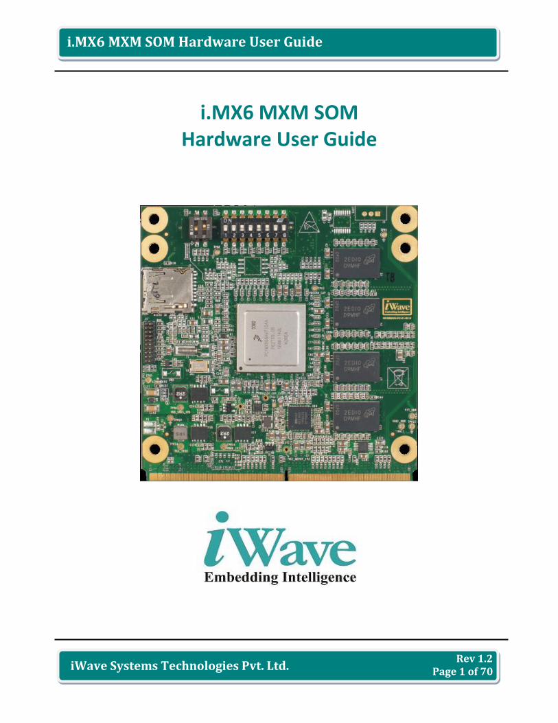
i.MX6 MXM SOM Hardware User Guide - iWave Systems Modules/i.MX6_… · i.MX6 MXM SOM Hardware User...
70
Rev 1.2 Page 1 of 70 i.MX6 MXM SOM Hardware User Guide iWave Systems Technologies Pvt. Ltd. i.MX6 MXM SOM Hardware User Guide
Transcript of i.MX6 MXM SOM Hardware User Guide - iWave Systems Modules/i.MX6_… · i.MX6 MXM SOM Hardware User...
Rev 1.2 Page 1 of 70
i.MX6 MXM SOM Hardware User Guide
iWave Systems Technologies Pvt. Ltd.
i.MX6 MXM SOM Hardware User Guide
Rev 1.2 Page 2 of 70
i.MX6 MXM SOM Hardware User Guide
iWave Systems Technologies Pvt. Ltd.
Document Revision History
Revision Date Description Authors
0.1 28-03-2012 Initial Draft Version Roshan D’souza
1.0 26-05-2012 Optional interface details, Mechanical details updated
Roshan D’souza
1.1 31-05-2012 Updated optional interface section table & boot configuration pins schematics added
Roshan D’souza
1.2 04-07-2012 RGMII signals level at Expansion connector pinouts table are updated
Roshan D’souza
PROPRIETARY NOTICE: This document contains proprietary material for the sole use of the intended recipient(s). Do not read this document if you are not the intended recipient. Any review, use, distribution or disclosure by others is strictly prohibited. If you are not the intended recipient (or authorized to receive for the recipient), you are hereby notified that any disclosure, copying distribution or use of any of the information contained within this document is STRICTLY PROHIBITED. Thank you. “iWave Systems Tech. Pvt. Ltd.”
Rev 1.2 Page 3 of 70
i.MX6 MXM SOM Hardware User Guide
iWave Systems Technologies Pvt. Ltd.
Table of Contents
1. INTRODUCTION .............................................................................................................. 7
1.1 Purpose ............................................................................................................................... 7
1.2 MXM SOM Overview .......................................................................................................... 7
1.3 i.MX6 MXM SOM Features ................................................................................................. 7
1.4 List of Acronyms .................................................................................................................. 9
1.5 References ........................................................................................................................ 10
2. i.MX6 SOM ARCHITECTURE AND DESIGN ...................................................................... 11
2.1 i.MX6 MXM SOM Block Diagram ...................................................................................... 11
2.2 i.MX6 MXM SOM TOP VIEW ............................................................................................. 12
2.3 i.MX6 MXM SOM BOTTOM VIEW ..................................................................................... 13
2.4 i.MX6 CPU ......................................................................................................................... 14 2.4.1 Boot Mode Settings .................................................................................................. 14 2.4.2 Boot Device Settings ................................................................................................. 15
2.5 Memory ............................................................................................................................. 16 2.5.1 DDR3 SDRAM ............................................................................................................ 16 2.5.2 eMMC Flash Memory ............................................................................................... 17 2.5.3 Micro SD Slot (Optional) ........................................................................................... 17 2.5.4 SPI NOR Flash Memory (Optional) ............................................................................ 18
2.6 3Pin RS232 Debug UART Debug Connector (Optional) .................................................... 20
2.7 JTAG Connector (Optional) ............................................................................................... 21
2.8 MXM PCB Edge Connector ................................................................................................ 23
2.9 Expansion Connector ........................................................................................................ 42
2.10 Shared/muxed signals in MXM SOM ............................................................................ 45
3. i.M6 MXM SOM USAGE REQUIREMENT ........................................................................ 53
3.1 Power Supply Requirement .............................................................................................. 53
3.2 Power Consumption ......................................................................................................... 53
3.3 Power ON sequence Requirement ................................................................................... 55
Rev 1.2 Page 4 of 70
i.MX6 MXM SOM Hardware User Guide
iWave Systems Technologies Pvt. Ltd.
3.4 Power Related signals at Edge connector ......................................................................... 55
3.5 LED Description ................................................................................................................. 57
3.6 i.MX6 MXM SOM Interface Requirement ......................................................................... 57 3.6.1 PCIE Interface Requirement ...................................................................................... 57 3.6.2 SATA Interface Requirement .................................................................................... 57 3.6.3 LVDS Interface requirement ..................................................................................... 58 3.6.4 RGMII Interface Requirement ................................................................................... 58 3.6.5 MIPI DSI & CSI Interface Requirement ...................................................................... 59 3.6.6 HDMI Interface Requirement ................................................................................... 59 3.6.7 MLB Interface Requirement ..................................................................................... 60
3.7 ON Module IO Muxing ...................................................................................................... 61
4. MECHANICAL INFORMATION ....................................................................................... 64
4.1 Mechanical Dimensions of i.MX6 MXM SOM ................................................................... 64
4.2 Mating Connector Details ................................................................................................. 66
4.3 Connector’s placement details in MXM carrier card ........................................................ 66
4.4 Guidelines to insert the CPU board into Carrier board .................................................... 68
5. ORDERING INFORMATION ........................................................................................... 69
6. TECHNICAL SUPPORT ................................................................................................... 70
Rev 1.2 Page 5 of 70
i.MX6 MXM SOM Hardware User Guide
iWave Systems Technologies Pvt. Ltd.
List of Figures FIGURE 1: I.MX6 MXM SOM BLOCK DIAGRAM ..................................................................................... 11
FIGURE 2: I.MX6 MXM SOM TOP VIEW ............................................................................................ 12
FIGURE 3: I.MX6 MXM SOM BOTTOM VIEW ................................................................................... 13
FIGURE 4: BOOT DEVICE SETTINGS SWITCH ............................................................................................. 15
FIGURE 5: BOOT CONFIGURATION PINS .................................................................................................. 16
FIGURE 6: MICRO SD CONNECTOR ........................................................................................................ 17
FIGURE 7: SPI NOR FLASH SCHEMATIC .................................................................................................. 19
FIGURE 8: UART CONNECTOR ............................................................................................................. 20
FIGURE 9: RS232 3PIN HEADER SCHEMATIC .......................................................................................... 21
FIGURE 10: JTAG CONNECTOR ............................................................................................................ 22
FIGURE 11: MXM RVS PCB EDGE CONNECTOR ..................................................................................... 23
FIGURE 12: EXPANSION CONNECTOR ..................................................................................................... 42
FIGURE 13: 2PIN POWER CONNECTOR ................................................................................................... 53
FIGURE 14: POWER ON SEQUENCE ....................................................................................................... 55
FIGURE 15: PCIE INTERFACE REQUIREMENT ........................................................................................... 57
FIGURE 16: SATA INTERFACE REQUIREMENT .......................................................................................... 58
FIGURE 17: LVDS INTERFACE REQUIREMENT ........................................................................................... 58
FIGURE 18: MIPI DSI & CSI INTERFACE REQUIREMENT ............................................................................ 59
FIGURE 19: HDMI INTERFACE REQUIREMENT ......................................................................................... 60
FIGURE 20: MLB INTERFACE REQUIREMENT ........................................................................................... 60
FIGURE 21: I.MX6 MXM SOM TOP - DIMENSIONS ............................................................................... 64
FIGURE 22: I.MX6 MXM SOM BOTTOM - DIMENSIONS ....................................................................... 65
FIGURE 23: CONNECTORS PLACEMENT DETAILS IN CARRIER CARD ................................................................. 67
FIGURE 24: MXM SOM INSERTION PROCEDURE ..................................................................................... 68
Rev 1.2 Page 6 of 70
i.MX6 MXM SOM Hardware User Guide
iWave Systems Technologies Pvt. Ltd.
List of Tables TABLE 1: ACRONYMS & ABBREVIATIONS .................................................................................................. 9
TABLE 2: BOOT MODE SETTINGS .......................................................................................................... 15
TABLE 3: BOOT DEVICE SETTINGS .......................................................................................................... 15
TABLE 4: MICRO SD CONNECTOR (OPTIONAL) PIN ASSIGNMENT ................................................................ 17
TABLE 5: BOM FOR SPI NOR FLASH CIRCUIT.......................................................................................... 19
TABLE 6: RS232 3PIN HEADER (OPTIONAL) PIN ASSIGNMENT ................................................................... 20
TABLE 7: BOM FOR RS232 3PIN HEADER CIRCUIT .................................................................................. 21
TABLE 8: JTAG HEADER (OPTIONAL) PIN ASSIGNMENT ............................................................................ 22
TABLE 9: MXM RVS PCB EDGE CONNECTOR TOP PIN ASSIGNMENT ......................................................... 24
TABLE 10: MXM RVS PCB EDGE CONNECTOR (J4) BOTTOM PIN ASSIGNMENT ......................................... 32
TABLE 11: EXPANSION CONNECTOR (J5) PIN ASSIGNMENT ........................................................................ 43
TABLE 12: SHARED/MUXED SIGNALS ...................................................................................................... 45
TABLE 13: 2PIN POWER CONNECTOR .................................................................................................... 53
TABLE 14: POWER REQUIREMENT TABLE ................................................................................................ 54
TABLE 15: POWER RELATED SIGNALS AT EDGE CONNECTOR TABLE............................................................... 55
TABLE 16: ON MODULE IO MUXING ..................................................................................................... 61
TABLE 17: MATING CONNECTOR DETAILS ............................................................................................... 66
TABLE 18: ORDERING INFORMATION ..................................................................................................... 69
Rev 1.2 Page 7 of 70
i.MX6 MXM SOM Hardware User Guide
iWave Systems Technologies Pvt. Ltd.
1. INTRODUCTION
1.1 Purpose
This document is the Hardware User Guide for the i.MX6 MXM SOM based on the Freescale’s i.MX6 Applications Processor. This Guide provides detailed information on the overall design and usage of the i.MX6 MXM SOM from a Hardware System perspective.
1.2 MXM SOM Overview
The i.MX6 MXM SOM is extension of i.MX6 CPU and plays the role between Single Board Computer (SBC) and the i.MX6 SOC. With the SOM approach one can get the best aspects of both buying an Off-The-Shelf SBC board and a Custom design solution. A single ruggedized MXM connector provides the carrier board interface to carry all the I/O signals to and from the MXM module. The MXM -3 Edge connector pin outs are fully compatible with i.MX53 MXM SOM. The Module can be validated with iW-Rainbow-G11D platform except the signals coming out at the Edge connector.
1.3 i.MX6 MXM SOM Features
The i.MX6 MXM SOM will support the following features. CPU
Freescale’s i.MX6 Quad/Dual/Solo CPUs: ARM Cortex A9, each @ 1GHz
Memory
1GB DDR3 (Expandable up to 4GB)
4GB eMMC Flash (Expandable up to 32GB)
Micro SD (Optional)
SPI NOR Flash (Optional)
NAND Flash(Optional)1 1 NAND Flash signals are shared with eMMC. Please contact iWave for NAND flash Support.
On Board peripherals support
MXM PCB Edge Connector
PCIe v2.0 (1 No.)
SATA II (1 No.)
USB OTG 2.0 (1 No.)
USB Host 2.0 (1 No.)
Rev 1.2 Page 8 of 70
i.MX6 MXM SOM Hardware User Guide
iWave Systems Technologies Pvt. Ltd.
LVDS (2 Nos.)
LCD - 24bpp RGB (1 No.)
I2S Audio (1 No.)
Gigabit Ethernet through On-SOM Gigabit Ethernet PHY (1 No.)2
SD/SDIO/MMC (2 Nos.)
I2C (3 Nos.)
SPI (1No.)
CAN (2 Nos.)
UART (3 Nos.)
CSI (2 Nos.)
ESAI (1No.)
SPDIF (1No.)
MLB 3 Pin (1No.)
17 GPIOs (Minimum)
5V Input Power
Expansion Connector
HDMI (1 No.)
MIPI-DSI (1 No.)
MIPI-CSI (1 No.)
MLB 6 Pin ((1 No.)
RGMII (1 No.)2
ENET (Optional) 2 Either PHY output OR RGMII signals can be used at a time.
3pin RS232 Debug UART Header (optional)
20 pin JTAG Header (optional)
Switches
Boot Mode Settings Switch
Boot Device Settings Switch
Power Supply
2pin Power In Header(optional)
Temperature Supported
-40°C to +85°C
Form Factor
85mm X 85mm

Rev 1.2 Page 9 of 70
i.MX6 MXM SOM Hardware User Guide
iWave Systems Technologies Pvt. Ltd.
1.4 List of Acronyms
The following acronyms will be used throughout this document.
Table 1: Acronyms & Abbreviations
Acronyms Description
ARM Advanced RISC Machine
BPP Bits Per Pixel
CAN Controller Area Network
DDR3 Double Data Rate 3
DSI Display Serial Interface
eCSPI Enhanced Configurable Serial Peripheral Interface
eMMC Embedded Multi Media Card
ESAI Enhanced Serial Audio Interface
GB Giga Byte
Gbps Giga bits per sec
GPIO General Purpose Input Output
HDMI High-Definition Multimedia Interface
I2C Inter-Integrated Circuit
IC Integrated Circuit
JTAG Joint Test Action Group
Kbps Kilobits per second
LCD Liquid Crystal Display
LVDS Low Voltage Differential Signal
MB Mega Byte
Mbps Mega bits per sec
MHz Mega Hertz
MIPI Mobile Industry CPU Interface
MLB Media Local Bus
MMC Multi Media Card
mSEC milli Second
MXM Mobile PCI Express Module
PCB Printed Circuit board
PWM Pulse Width Modulation
RGMII Reduced Gigabit Media Independent Interface
RTC Real Time Clock
SATA Serial Advanced Technology Attachment
SD Secure Digital
Rev 1.2 Page 10 of 70
i.MX6 MXM SOM Hardware User Guide
iWave Systems Technologies Pvt. Ltd.
SDIO Secure Digital Input Output
SOM System On Module
SPI Serial Peripheral Interface
SPDIF Sony/Philips Digital Interconnect Format
SSI Synchronous Serial Interface
UART Universal Asynchronous Receiver/Transmitters
USB Universal Serial bus
USBOTG Universal Serial bus On The Go
V Voltage
1.5 References
i.MX6 Applications Processors Products Datasheet
i.MX6 Applications Processor Reference Manual
i.MX53 SOM http://www.iwavesystems.com/?q=node/130
Rainbow-G11D http://www.iwavesystems.com/?q=node/139
Rev 1.2 Page 11 of 70
i.MX6 MXM SOM Hardware User Guide
iWave Systems Technologies Pvt. Ltd.
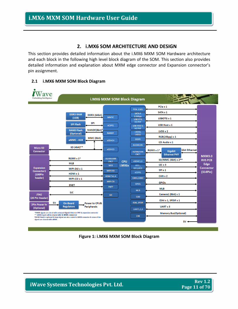
2. i.MX6 SOM ARCHITECTURE AND DESIGN
This section provides detailed information about the i.MX6 MXM SOM Hardware architecture and each block in the following high level block diagram of the SOM. This section also provides detailed information and explanation about MXM edge connector and Expansion connector’s pin assignment.
2.1 i.MX6 MXM SOM Block Diagram
Figure 1: i.MX6 MXM SOM Block Diagram
Rev 1.2 Page 12 of 70
i.MX6 MXM SOM Hardware User Guide
iWave Systems Technologies Pvt. Ltd.
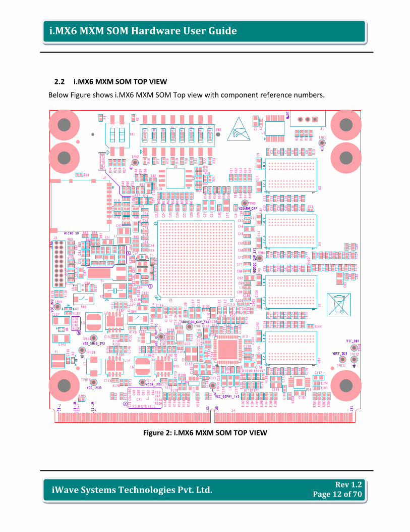
2.2 i.MX6 MXM SOM TOP VIEW
Below Figure shows i.MX6 MXM SOM Top view with component reference numbers.
Figure 2: i.MX6 MXM SOM TOP VIEW
Rev 1.2 Page 13 of 70
i.MX6 MXM SOM Hardware User Guide
iWave Systems Technologies Pvt. Ltd.
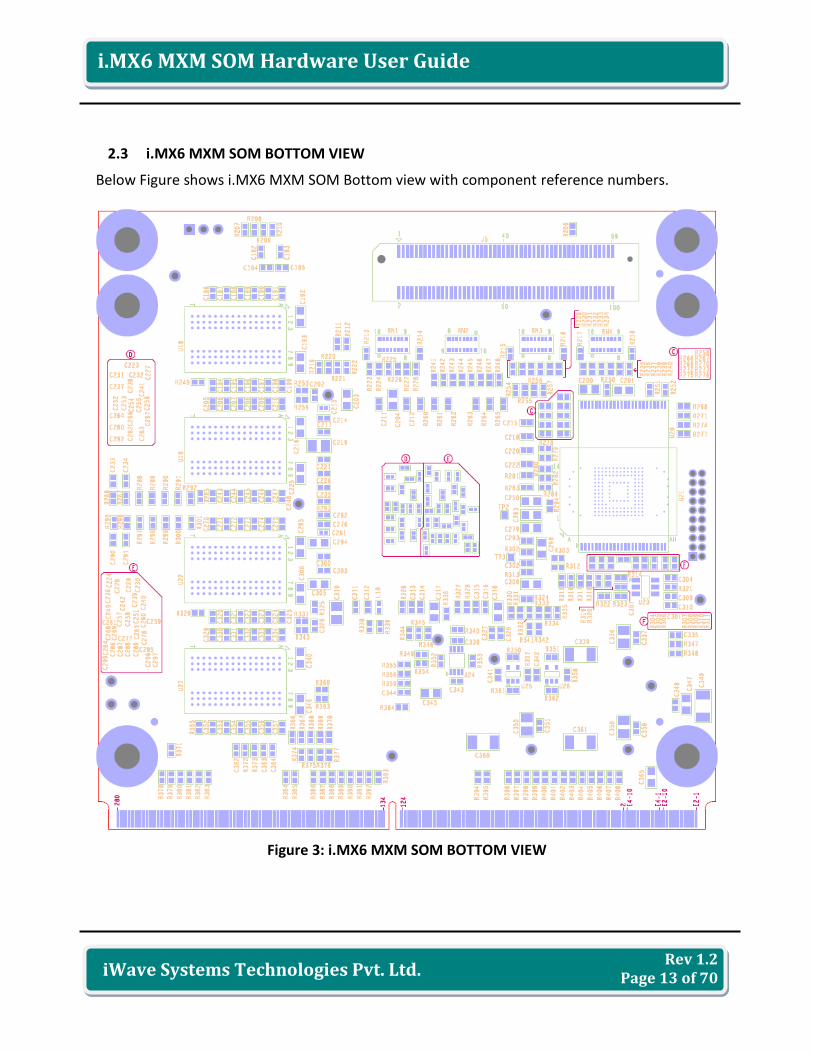
2.3 i.MX6 MXM SOM BOTTOM VIEW
Below Figure shows i.MX6 MXM SOM Bottom view with component reference numbers.
Figure 3: i.MX6 MXM SOM BOTTOM VIEW

Rev 1.2 Page 14 of 70
i.MX6 MXM SOM Hardware User Guide
iWave Systems Technologies Pvt. Ltd.
2.4 i.MX6 CPU
The i.MX6 Quad/Dual/Solo CPU represent Freescale’s latest achievement in integrated multimedia application CPUs, which are part of a growing family of multimedia-focused products that offer high performance processing and are optimized for lowest power consumption. The CPU features Freescale’s advanced implementation of the quad ARM™ Cortex-A9 core, which operates at speeds up to 1 GHz. They include 2D and 3D graphics CPUs, 3D 1080p video processing, and integrated power management. Each CPU provides a 64-bit DDR3/LVDDR3-1066 memory interface and a number of other interfaces for connecting peripherals, such as WLAN, Bluetooth™, GPS, hard drive, displays, and camera sensors. The i.MX6 MXM SOM supports i.MX6 Quad, Dual, Dual Lite & Solo series of i.MX6 CPU. By default i.MX6 Quad CPU is supported. Please contact iWave for other series of i.MX6 MXM SOM. The i.MX6 Applications CPU is physically located in the central portion of the SOM. The information for voltage levels and other chip specific details come from the i.MX6 Data Sheet, which may be revised from time to time. Every effort will be made to keep this User Guide to the most recent Data Sheet. Note: Please see the latest datasheet from Freescale website for Electrical characteristics of i.MX6 Application CPU.
2.4.1 Boot Mode Settings
The i.MX6 Boot ROM code uses the state of the internal register BOOT_MODE [1:0] as well as the state of various eFUSEs and/or GPIO settings to determine the boot flow behaviour of the device. The i.MX6 boot process begins at Power On Reset (POR) where the hardware reset logic forces the ARM core to begin execution starting from the on-chip boot ROM. The below table provides the boot modes along with boot mode selection pin settings for the i.MX6 MXM SOM.
Rev 1.2 Page 15 of 70
i.MX6 MXM SOM Hardware User Guide
iWave Systems Technologies Pvt. Ltd.
Table 2: Boot Mode Settings
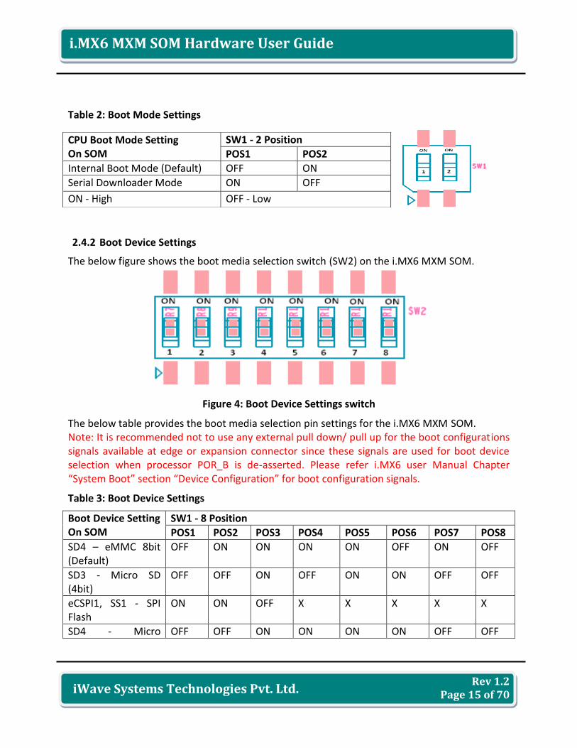
2.4.2 Boot Device Settings
The below figure shows the boot media selection switch (SW2) on the i.MX6 MXM SOM.
Figure 4: Boot Device Settings switch
The below table provides the boot media selection pin settings for the i.MX6 MXM SOM. Note: It is recommended not to use any external pull down/ pull up for the boot configurations signals available at edge or expansion connector since these signals are used for boot device selection when processor POR_B is de-asserted. Please refer i.MX6 user Manual Chapter “System Boot” section “Device Configuration” for boot configuration signals.
Table 3: Boot Device Settings
Boot Device Setting On SOM
SW1 - 8 Position
POS1 POS2 POS3 POS4 POS5 POS6 POS7 POS8
SD4 – eMMC 8bit (Default)
OFF ON ON ON ON OFF ON OFF
SD3 - Micro SD (4bit)
OFF OFF ON OFF ON ON OFF OFF
eCSPI1, SS1 - SPI Flash
ON ON OFF X X X X X
SD4 - Micro OFF OFF ON ON ON ON OFF OFF
CPU Boot Mode Setting On SOM
SW1 - 2 Position
POS1 POS2
Internal Boot Mode (Default) OFF ON
Serial Downloader Mode ON OFF
ON - High OFF - Low
Rev 1.2 Page 16 of 70
i.MX6 MXM SOM Hardware User Guide
iWave Systems Technologies Pvt. Ltd.
SD(4bit)
SATA - 3Gbps OFF ON OFF OFF OFF X X X
ON - High OFF - Low X - Don't Care
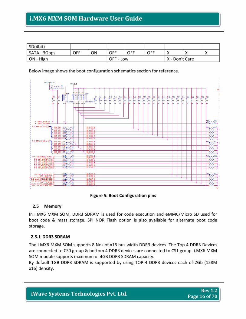
Below image shows the boot configuration schematics section for reference.
Figure 5: Boot Configuration pins
2.5 Memory
In i.MX6 MXM SOM, DDR3 SDRAM is used for code execution and eMMC/Micro SD used for boot code & mass storage. SPI NOR Flash option is also available for alternate boot code storage.
2.5.1 DDR3 SDRAM
The i.MX6 MXM SOM supports 8 Nos of x16 bus width DDR3 devices. The Top 4 DDR3 Devices are connected to CS0 group & bottom 4 DDR3 devices are connected to CS1 group. i.MX6 MXM SOM module supports maximum of 4GB DDR3 SDRAM capacity. By default 1GB DDR3 SDRAM is supported by using TOP 4 DDR3 devices each of 2Gb (128M x16) density.
Rev 1.2 Page 17 of 70
i.MX6 MXM SOM Hardware User Guide
iWave Systems Technologies Pvt. Ltd.
Developers should note that using different configurations of SDRAM requires register changes on the i.MX6 CPU to ensure that timing and address sequencing is set up correctly. Software initialization settings will be different depending on SDRAM configuration.
2.5.2 eMMC Flash Memory
The i.MX6 MXM SOM supports eMMC memory as an mass storage and boot device. eMMC is connected to the eSDHC channel 4 (SD4) module of the i.MX6 CPU. This device will operate under 3.3 Voltage. By default 4GB capacity eMMC flash will be mounted on the SOM.
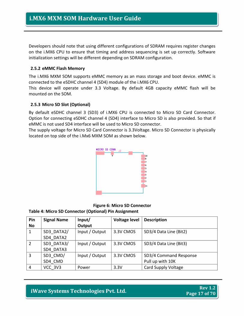
2.5.3 Micro SD Slot (Optional)
By default eSDHC channel 3 (SD3) of i.MX6 CPU is connected to Micro SD Card Connector. Option for connecting eSDHC channel 4 (SD4) interface to Micro SD is also provided. So that if eMMC is not used SD4 interface will be used to Micro SD connector. The supply voltage for Micro SD Card Connector is 3.3Voltage. Micro SD Connector is physically located on top side of the i.Mx6 MXM SOM as shown below.
Figure 6: Micro SD Connector Table 4: Micro SD Connector (Optional) Pin Assignment
Pin No
Signal Name Input/ Output
Voltage level Description
1 SD3_DATA2/ SD4_DATA2
Input / Output 3.3V CMOS SD3/4 Data Line (Bit2)
2 SD3_DATA3/ SD4_DATA3
Input / Output 3.3V CMOS SD3/4 Data Line (Bit3)
3 SD3_CMD/ SD4_CMD
Input / Output 3.3V CMOS SD3/4 Command Response Pull up with 10K
4 VCC_3V3 Power 3.3V Card Supply Voltage
Rev 1.2 Page 18 of 70
i.MX6 MXM SOM Hardware User Guide
iWave Systems Technologies Pvt. Ltd.
5 SD3_CLK/ SD4_CLK
Output 3.3V CMOS SD3/4 Clock
6 VSS Power GND Ground
7 SD3_DATA0/ SD4_DATA0
Input / Output 3.3V CMOS SD3/4 Data Line (Bit0)
8 SD3_DATA1/ SD4_DATA1
Input / Output 3.3V CMOS SD3/4 Data Line (Bit1)
9 gpio1_GPIO30 (ENET_TXD0)
Input 3.3V CMOS Micro SD Card Detect Pull up with 10K
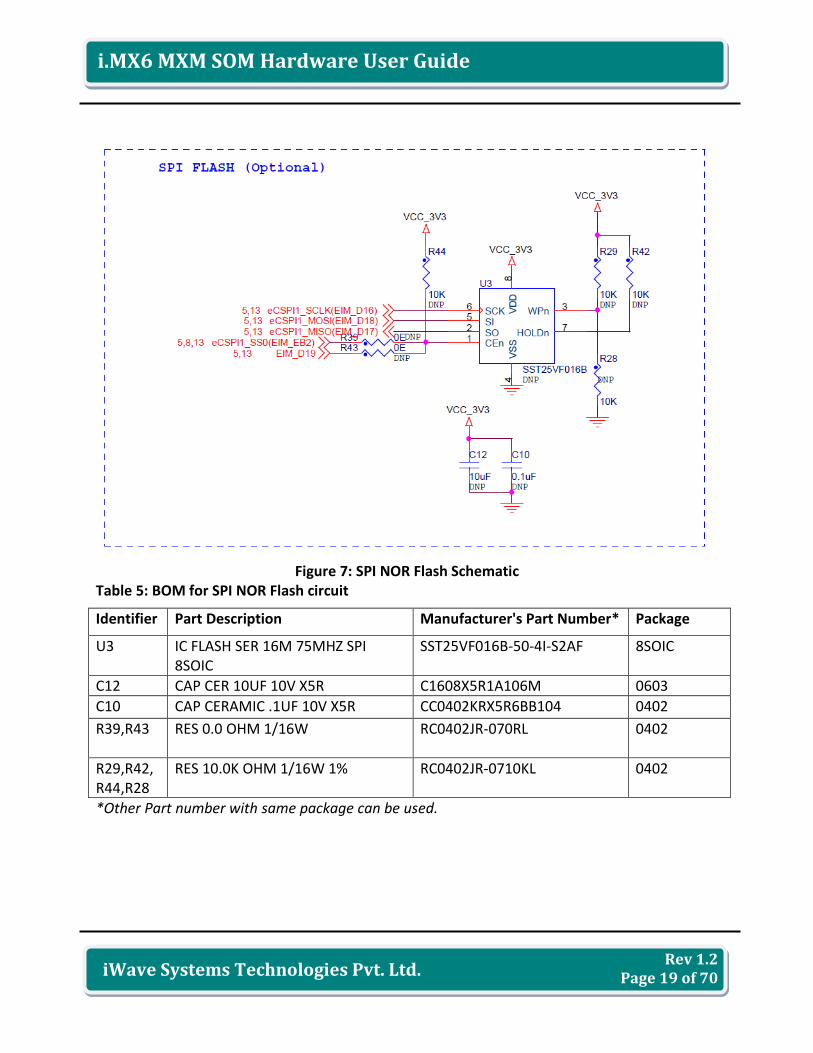
2.5.4 SPI NOR Flash Memory (Optional)
The i.MX6 MXM SOM supports SPI NOR Flash as an alternate Boot Device. eCSPI1 interface with SS1 is used for SPI NOR Flash. This device operates under 3.3 Voltage level. This is the optional feature and will not be populated in default configuration.
The SPI NOR Flash memory can be used in i.MX6 MXM SOM by mounting the components shown in the below schematic diagram and also BOM details are given in below table.
Rev 1.2 Page 19 of 70
i.MX6 MXM SOM Hardware User Guide
iWave Systems Technologies Pvt. Ltd.
Figure 7: SPI NOR Flash Schematic Table 5: BOM for SPI NOR Flash circuit
Identifier Part Description Manufacturer's Part Number* Package
U3 IC FLASH SER 16M 75MHZ SPI 8SOIC
SST25VF016B-50-4I-S2AF 8SOIC
C12 CAP CER 10UF 10V X5R C1608X5R1A106M 0603
C10 CAP CERAMIC .1UF 10V X5R CC0402KRX5R6BB104 0402
R39,R43
RES 0.0 OHM 1/16W RC0402JR-070RL 0402
R29,R42,R44,R28
RES 10.0K OHM 1/16W 1% RC0402JR-0710KL 0402
*Other Part number with same package can be used.
Rev 1.2 Page 20 of 70
i.MX6 MXM SOM Hardware User Guide
iWave Systems Technologies Pvt. Ltd.
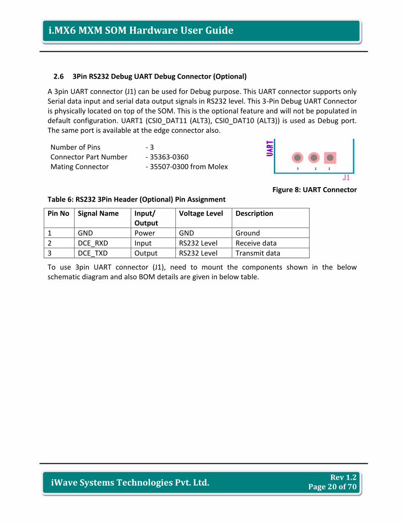
2.6 3Pin RS232 Debug UART Debug Connector (Optional)
A 3pin UART connector (J1) can be used for Debug purpose. This UART connector supports only Serial data input and serial data output signals in RS232 level. This 3-Pin Debug UART Connector is physically located on top of the SOM. This is the optional feature and will not be populated in default configuration. UART1 (CSI0_DAT11 (ALT3), CSI0_DAT10 (ALT3)) is used as Debug port. The same port is available at the edge connector also.
Figure 8: UART Connector Table 6: RS232 3Pin Header (Optional) Pin Assignment
Pin No Signal Name Input/ Output
Voltage Level Description
1 GND Power GND Ground
2 DCE_RXD Input RS232 Level Receive data
3 DCE_TXD Output RS232 Level Transmit data
To use 3pin UART connector (J1), need to mount the components shown in the below schematic diagram and also BOM details are given in below table.
Number of Pins - 3 Connector Part Number - 35363-0360 Mating Connector - 35507-0300 from Molex
Rev 1.2 Page 21 of 70
i.MX6 MXM SOM Hardware User Guide
iWave Systems Technologies Pvt. Ltd.
Figure 9: RS232 3Pin Header Schematic Table 7: BOM for RS232 3Pin Header circuit
Identifier Part Description Manufacturer's Part Number* Package
U1 IC DRVR/RCVR MLTCH RS232 16TSSOP
MAX3232IPWR 16Pin TSSOP
C1 CAP CER 10UF 10V X5R C1608X5R1A106M 0603
C2,C182, C183,C184,C185
CAP CERAMIC .1UF 10V X5R
CC0402KRX5R6BB104 0402
R3,R4,R5,R6,R207,R208,R209,R210
RES 0.0 OHM 1/16W RC0402JR-070RL 0402
J1 CONN HEADER 3POS 2MM R/A TIN
35363-0360 3Pin TH
*Other Part number with same package can be used.
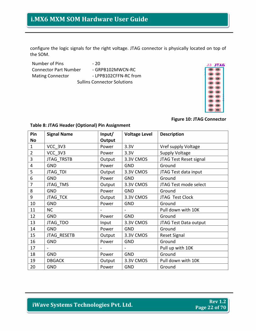
2.7 JTAG Connector (Optional)
A customized 20-pin ARM JTAG connector is available in i.MX6 MXM SOM for Debug purpose. 3.3V reference power is provided to pin 1 of the connector to allow JTAG tool to automatically
Rev 1.2 Page 22 of 70
i.MX6 MXM SOM Hardware User Guide
iWave Systems Technologies Pvt. Ltd.
configure the logic signals for the right voltage. JTAG connector is physically located on top of the SOM.
Figure 10: JTAG Connector Table 8: JTAG Header (Optional) Pin Assignment
Pin No
Signal Name Input/ Output
Voltage Level Description
1 VCC_3V3 Power 3.3V Vref supply Voltage
2 VCC_3V3 Power 3.3V Supply Voltage
3 JTAG_TRSTB Output 3.3V CMOS JTAG Test Reset signal
4 GND Power GND Ground
5 JTAG_TDI Output 3.3V CMOS JTAG Test data input
6 GND Power GND Ground
7 JTAG_TMS Output 3.3V CMOS JTAG Test mode select
8 GND Power GND Ground
9 JTAG_TCK Output 3.3V CMOS JTAG Test Clock
10 GND Power GND Ground
11 NC - - Pull down with 10K
12 GND Power GND Ground
13 JTAG_TDO Input 3.3V CMOS JTAG Test Data output
14 GND Power GND Ground
15 JTAG_RESETB Output 3.3V CMOS Reset Signal
16 GND Power GND Ground
17 - - - Pull up with 10K
18 GND Power GND Ground
19 DBGACK Output 3.3V CMOS Pull down with 10K
20 GND Power GND Ground
Number of Pins - 20 Connector Part Number - GRPB102MWCN-RC Mating Connector - LPPB102CFFN-RC from
Sullins Connector Solutions
Rev 1.2 Page 23 of 70
i.MX6 MXM SOM Hardware User Guide
iWave Systems Technologies Pvt. Ltd.
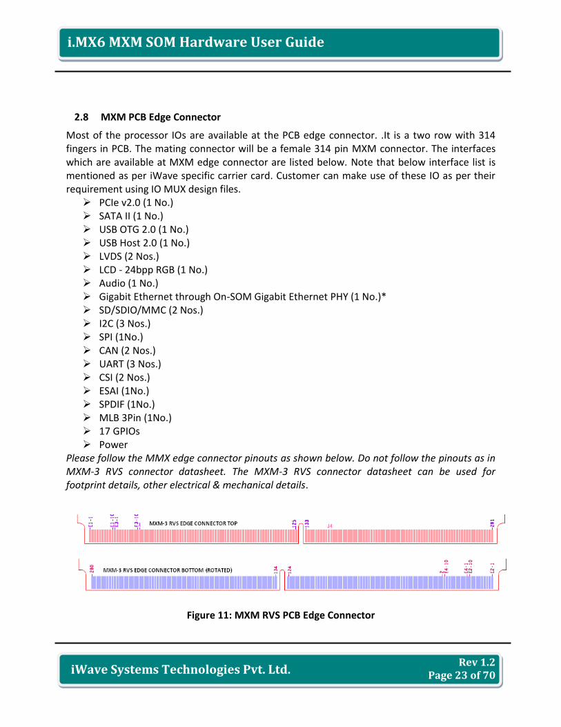
2.8 MXM PCB Edge Connector
Most of the processor IOs are available at the PCB edge connector. .It is a two row with 314 fingers in PCB. The mating connector will be a female 314 pin MXM connector. The interfaces which are available at MXM edge connector are listed below. Note that below interface list is mentioned as per iWave specific carrier card. Customer can make use of these IO as per their requirement using IO MUX design files. PCIe v2.0 (1 No.) SATA II (1 No.) USB OTG 2.0 (1 No.) USB Host 2.0 (1 No.) LVDS (2 Nos.) LCD - 24bpp RGB (1 No.) Audio (1 No.) Gigabit Ethernet through On-SOM Gigabit Ethernet PHY (1 No.)* SD/SDIO/MMC (2 Nos.) I2C (3 Nos.) SPI (1No.) CAN (2 Nos.) UART (3 Nos.) CSI (2 Nos.) ESAI (1No.) SPDIF (1No.) MLB 3Pin (1No.) 17 GPIOs Power
Please follow the MMX edge connector pinouts as shown below. Do not follow the pinouts as in MXM-3 RVS connector datasheet. The MXM-3 RVS connector datasheet can be used for footprint details, other electrical & mechanical details.
Figure 11: MXM RVS PCB Edge Connector
Rev 1.2 Page 24 of 70
i.MX6 MXM SOM Hardware User Guide
iWave Systems Technologies Pvt. Ltd.
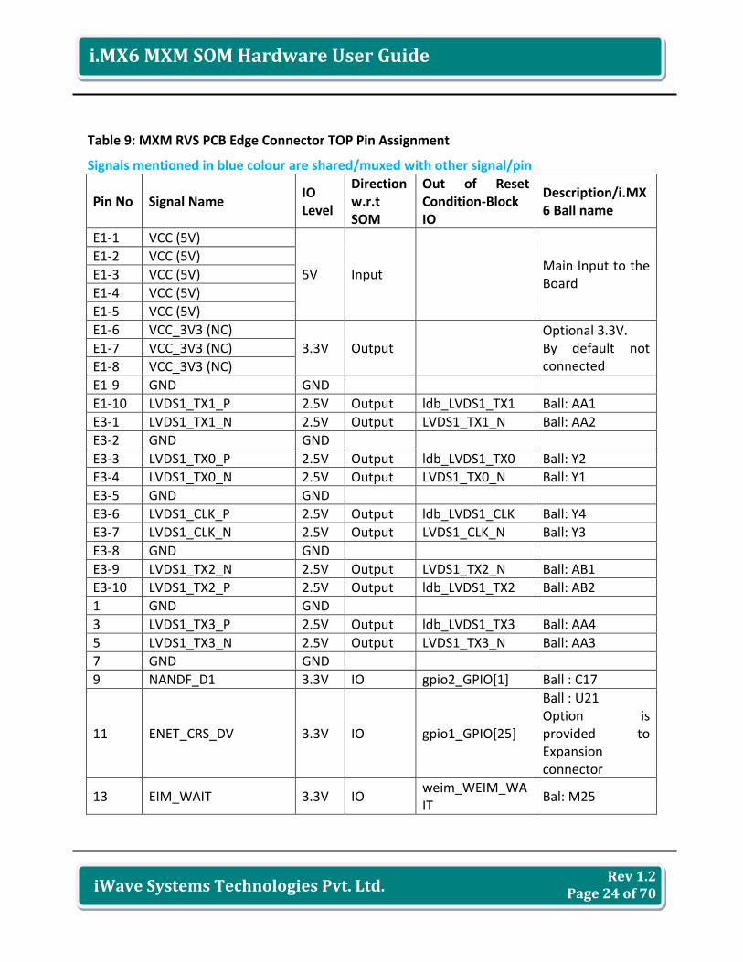
Table 9: MXM RVS PCB Edge Connector TOP Pin Assignment
Signals mentioned in blue colour are shared/muxed with other signal/pin
Pin No Signal Name IO Level
Direction w.r.t SOM
Out of Reset Condition-Block IO
Description/i.MX6 Ball name
E1-1 VCC (5V)
5V Input Main Input to the Board
E1-2 VCC (5V)
E1-3 VCC (5V)
E1-4 VCC (5V)
E1-5 VCC (5V)
E1-6 VCC_3V3 (NC)
3.3V Output Optional 3.3V. By default not connected
E1-7 VCC_3V3 (NC)
E1-8 VCC_3V3 (NC)
E1-9 GND GND
E1-10 LVDS1_TX1_P 2.5V Output ldb_LVDS1_TX1 Ball: AA1
E3-1 LVDS1_TX1_N 2.5V Output LVDS1_TX1_N Ball: AA2
E3-2 GND GND
E3-3 LVDS1_TX0_P 2.5V Output ldb_LVDS1_TX0 Ball: Y2
E3-4 LVDS1_TX0_N 2.5V Output LVDS1_TX0_N Ball: Y1
E3-5 GND GND
E3-6 LVDS1_CLK_P 2.5V Output ldb_LVDS1_CLK Ball: Y4
E3-7 LVDS1_CLK_N 2.5V Output LVDS1_CLK_N Ball: Y3
E3-8 GND GND
E3-9 LVDS1_TX2_N 2.5V Output LVDS1_TX2_N Ball: AB1
E3-10 LVDS1_TX2_P 2.5V Output ldb_LVDS1_TX2 Ball: AB2
1 GND GND
3 LVDS1_TX3_P 2.5V Output ldb_LVDS1_TX3 Ball: AA4
5 LVDS1_TX3_N 2.5V Output LVDS1_TX3_N Ball: AA3
7 GND GND
9 NANDF_D1 3.3V IO gpio2_GPIO[1] Ball : C17
11 ENET_CRS_DV 3.3V IO gpio1_GPIO[25]
Ball : U21 Option is provided to Expansion connector
13 EIM_WAIT 3.3V IO weim_WEIM_WAIT
Bal: M25
Rev 1.2 Page 25 of 70
i.MX6 MXM SOM Hardware User Guide
iWave Systems Technologies Pvt. Ltd.
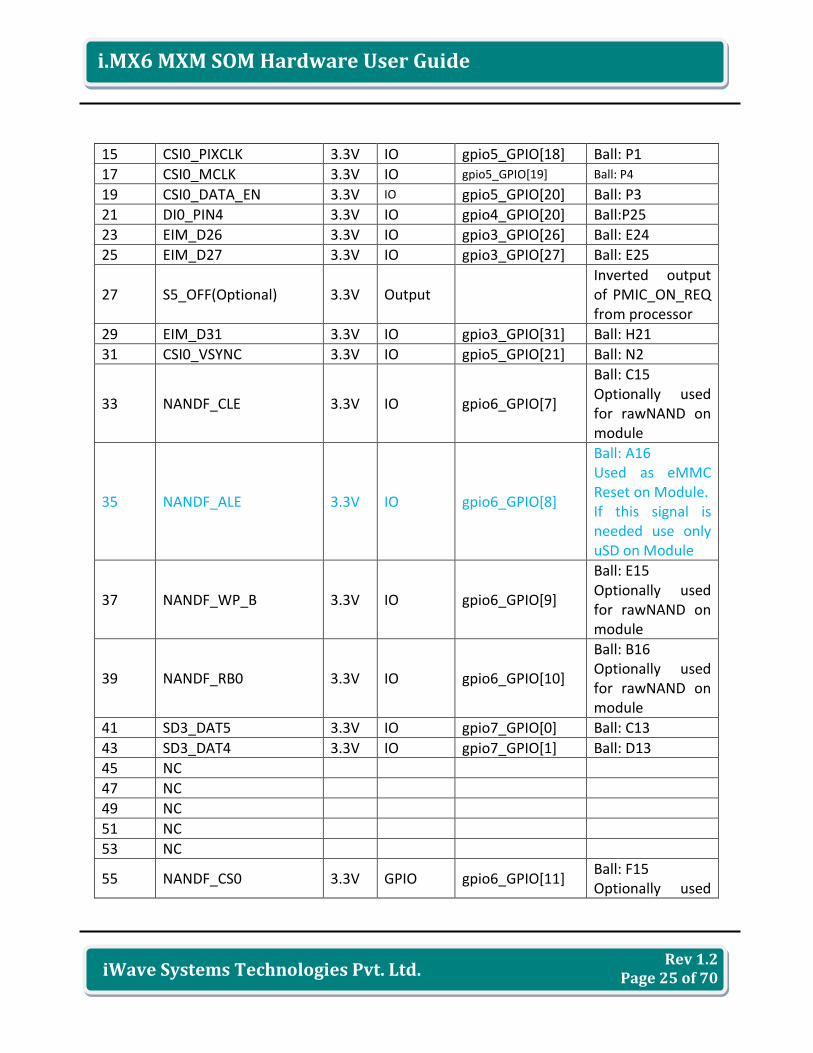
15 CSI0_PIXCLK 3.3V IO gpio5_GPIO[18] Ball: P1
17 CSI0_MCLK 3.3V IO gpio5_GPIO[19] Ball: P4
19 CSI0_DATA_EN 3.3V IO gpio5_GPIO[20] Ball: P3
21 DI0_PIN4 3.3V IO gpio4_GPIO[20] Ball:P25
23 EIM_D26 3.3V IO gpio3_GPIO[26] Ball: E24
25 EIM_D27 3.3V IO gpio3_GPIO[27] Ball: E25
27 S5_OFF(Optional) 3.3V Output Inverted output of PMIC_ON_REQ from processor
29 EIM_D31 3.3V IO gpio3_GPIO[31] Ball: H21
31 CSI0_VSYNC 3.3V IO gpio5_GPIO[21] Ball: N2
33 NANDF_CLE 3.3V IO gpio6_GPIO[7]
Ball: C15 Optionally used for rawNAND on module
35 NANDF_ALE 3.3V IO gpio6_GPIO[8]
Ball: A16 Used as eMMC Reset on Module. If this signal is needed use only uSD on Module
37 NANDF_WP_B 3.3V IO gpio6_GPIO[9]
Ball: E15 Optionally used for rawNAND on module
39 NANDF_RB0 3.3V IO gpio6_GPIO[10]
Ball: B16 Optionally used for rawNAND on module
41 SD3_DAT5 3.3V IO gpio7_GPIO[0] Ball: C13
43 SD3_DAT4 3.3V IO gpio7_GPIO[1] Ball: D13
45 NC
47 NC
49 NC
51 NC
53 NC
55 NANDF_CS0 3.3V GPIO gpio6_GPIO[11] Ball: F15 Optionally used
Rev 1.2 Page 26 of 70
i.MX6 MXM SOM Hardware User Guide
iWave Systems Technologies Pvt. Ltd.
for rawNAND on module
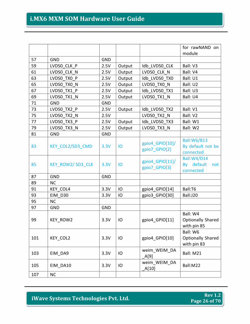
57 GND GND
59 LVDS0_CLK_P 2.5V Output ldb_LVDS0_CLK Ball: V3
61 LVDS0_CLK_N 2.5V Output LVDS0_CLK_N Ball: V4
63 LVDS0_TX0_P 2.5V Output ldb_LVDS0_TX0 Ball: U1
65 LVDS0_TX0_N 2.5V Output LVDS0_TX0_N Ball: U2
67 LVDS0_TX1_P 2.5V Output ldb_LVDS0_TX1 Ball: U3
69 LVDS0_TX1_N 2.5V Output LVDS0_TX1_N Ball: U4
71 GND GND
73 LVDS0_TX2_P 2.5V Output ldb_LVDS0_TX2 Ball: V1
75 LVDS0_TX2_N 2.5V LVDS0_TX2_N Ball: V2
77 LVDS0_TX3_P 2.5V Output ldb_LVDS0_TX3 Ball: W1
79 LVDS0_TX3_N 2.5V Output LVDS0_TX3_N Ball: W2
81 GND GND
83 KEY_COL2/SD3_CMD 3.3V IO gpio4_GPIO[10]/ gpio7_GPIO[2]
Ball:W6/B13 By default not be connected
85 KEY_ROW2/ SD3_CLK 3.3V IO gpio4_GPIO[11]/ gpio7_GPIO[3]
Ball:W4/D14 By default not connected
87 GND GND
89 NC
91 KEY_COL4 3.3V IO gpio4_GPIO[14] Ball:T6
93 EIM_D30 3.3V IO gpio3_GPIO[30] Ball:J20
95 NC
97 GND GND
99 KEY_ROW2 3.3V IO gpio4_GPIO[11] Ball: W4 Optionally Shared with pin 85
101 KEY_COL2 3.3V IO gpio4_GPIO[10] Ball: W6 Optionally Shared with pin 83
103 EIM_DA9 3.3V IO weim_WEIM_DA_A[9]
Ball: M21
105 EIM_DA10 3.3V IO weim_WEIM_DA_A[10]
Ball:M22
107 NC
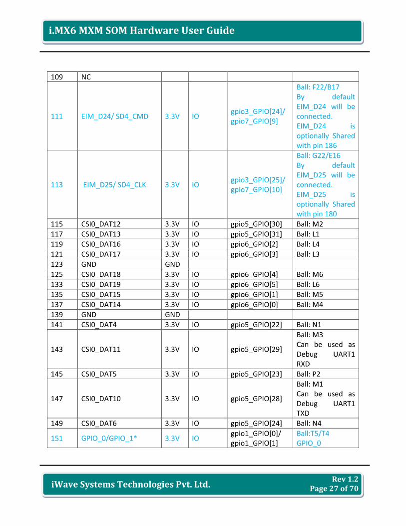
Rev 1.2 Page 27 of 70
i.MX6 MXM SOM Hardware User Guide
iWave Systems Technologies Pvt. Ltd.
109 NC
111 EIM_D24/ SD4_CMD 3.3V IO gpio3_GPIO[24]/ gpio7_GPIO[9]
Ball: F22/B17 By default EIM_D24 will be connected. EIM_D24 is optionally Shared with pin 186
113 EIM_D25/ SD4_CLK 3.3V IO gpio3_GPIO[25]/ gpio7_GPIO[10]
Ball: G22/E16 By default EIM_D25 will be connected. EIM_D25 is optionally Shared with pin 180
115 CSI0_DAT12 3.3V IO gpio5_GPIO[30] Ball: M2
117 CSI0_DAT13 3.3V IO gpio5_GPIO[31] Ball: L1
119 CSI0_DAT16 3.3V IO gpio6_GPIO[2] Ball: L4
121 CSI0_DAT17 3.3V IO gpio6_GPIO[3] Ball: L3
123 GND GND
125 CSI0_DAT18 3.3V IO gpio6_GPIO[4] Ball: M6
133 CSI0_DAT19 3.3V IO gpio6_GPIO[5] Ball: L6
135 CSI0_DAT15 3.3V IO gpio6_GPIO[1] Ball: M5
137 CSI0_DAT14 3.3V IO gpio6_GPIO[0] Ball: M4
139 GND GND
141 CSI0_DAT4 3.3V IO gpio5_GPIO[22] Ball: N1
143 CSI0_DAT11 3.3V IO gpio5_GPIO[29]
Ball: M3 Can be used as Debug UART1 RXD
145 CSI0_DAT5 3.3V IO gpio5_GPIO[23] Ball: P2
147 CSI0_DAT10 3.3V IO gpio5_GPIO[28]
Ball: M1 Can be used as Debug UART1 TXD
149 CSI0_DAT6 3.3V IO gpio5_GPIO[24] Ball: N4
151 GPIO_0/GPIO_1* 3.3V IO gpio1_GPIO[0]/ gpio1_GPIO[1]
Ball:T5/T4 GPIO_0
Rev 1.2 Page 28 of 70
i.MX6 MXM SOM Hardware User Guide
iWave Systems Technologies Pvt. Ltd.
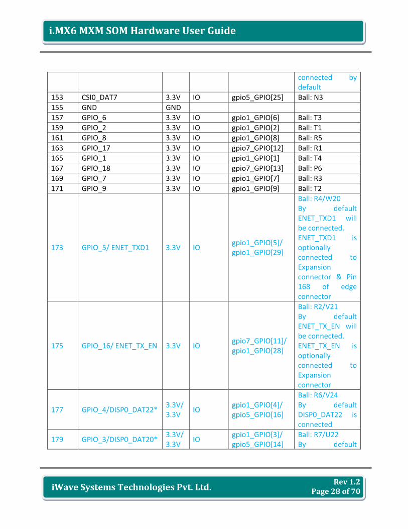
connected by default
153 CSI0_DAT7 3.3V IO gpio5_GPIO[25] Ball: N3
155 GND GND
157 GPIO_6 3.3V IO gpio1_GPIO[6] Ball: T3
159 GPIO_2 3.3V IO gpio1_GPIO[2] Ball: T1
161 GPIO_8 3.3V IO gpio1_GPIO[8] Ball: R5
163 GPIO_17 3.3V IO gpio7_GPIO[12] Ball: R1
165 GPIO_1 3.3V IO gpio1_GPIO[1] Ball: T4
167 GPIO_18 3.3V IO gpio7_GPIO[13] Ball: P6
169 GPIO_7 3.3V IO gpio1_GPIO[7] Ball: R3
171 GPIO_9 3.3V IO gpio1_GPIO[9] Ball: T2
173 GPIO_5/ ENET_TXD1 3.3V IO gpio1_GPIO[5]/ gpio1_GPIO[29]
Ball: R4/W20 By default ENET_TXD1 will be connected. ENET_TXD1 is optionally connected to Expansion connector & Pin 168 of edge connector
175 GPIO_16/ ENET_TX_EN 3.3V IO gpio7_GPIO[11]/ gpio1_GPIO[28]
Ball: R2/V21 By default ENET_TX_EN will be connected. ENET_TX_EN is optionally connected to Expansion connector
177 GPIO_4/DISP0_DAT22* 3.3V/3.3V
IO gpio1_GPIO[4]/ gpio5_GPIO[16]
Ball: R6/V24 By default DISP0_DAT22 is connected
179 GPIO_3/DISP0_DAT20* 3.3V/3.3V
IO gpio1_GPIO[3]/ gpio5_GPIO[14]
Ball: R7/U22 By default
Rev 1.2 Page 29 of 70
i.MX6 MXM SOM Hardware User Guide
iWave Systems Technologies Pvt. Ltd.
DISP0_DAT20 is connected
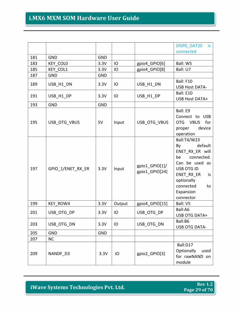
181 GND GND
183 KEY_COL0 3.3V IO gpio4_GPIO[6] Ball: W5
185 KEY_COL1 3.3V IO gpio4_GPIO[8] Ball: U7
187 GND GND
189 USB_H1_DN 3.3V IO USB_H1_DN Ball: F10 USB Host DATA-
191 USB_H1_DP 3.3V IO USB_H1_DP Ball: E10 USB Host DATA+
193 GND GND
195 USB_OTG_VBUS 5V Input USB_OTG_VBUS
Ball: E9 Connect to USB OTG VBUS for proper device operation
197 GPIO_1/ENET_RX_ER 3.3V Input gpio1_GPIO[1]/ gpio1_GPIO[24]
Ball:T4/W23 By default ENET_RX_ER will be connected. Can be used as USB OTG ID ENET_RX_ER is optionally connected to Expansion connector
199 KEY_ROW4 3.3V Output gpio4_GPIO[15] Ball: V5
201 USB_OTG_DP 3.3V IO USB_OTG_DP Ball:A6 USB OTG DATA+
203 USB_OTG_DN 3.3V IO USB_OTG_DN Ball:B6 USB OTG DATA-
205 GND GND
207 NC
209 NANDF_D3 3.3V IO gpio2_GPIO[3]
Ball:D17 Optionally used for rawNAND on module
Rev 1.2 Page 30 of 70
i.MX6 MXM SOM Hardware User Guide
iWave Systems Technologies Pvt. Ltd.
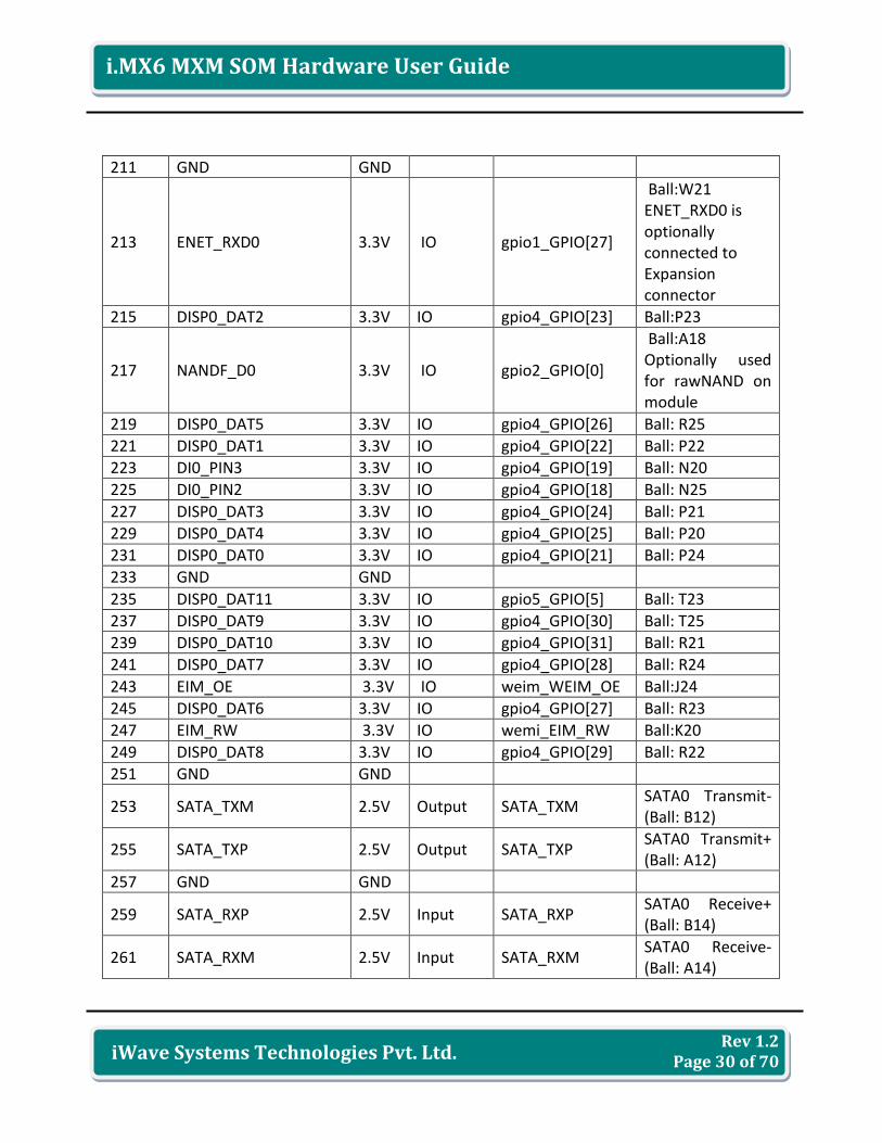
211 GND GND
213 ENET_RXD0 3.3V IO gpio1_GPIO[27]
Ball:W21 ENET_RXD0 is optionally connected to Expansion connector
215 DISP0_DAT2 3.3V IO gpio4_GPIO[23] Ball:P23
217 NANDF_D0 3.3V IO gpio2_GPIO[0]
Ball:A18 Optionally used for rawNAND on module
219 DISP0_DAT5 3.3V IO gpio4_GPIO[26] Ball: R25
221 DISP0_DAT1 3.3V IO gpio4_GPIO[22] Ball: P22
223 DI0_PIN3 3.3V IO gpio4_GPIO[19] Ball: N20
225 DI0_PIN2 3.3V IO gpio4_GPIO[18] Ball: N25
227 DISP0_DAT3 3.3V IO gpio4_GPIO[24] Ball: P21
229 DISP0_DAT4 3.3V IO gpio4_GPIO[25] Ball: P20
231 DISP0_DAT0 3.3V IO gpio4_GPIO[21] Ball: P24
233 GND GND
235 DISP0_DAT11 3.3V IO gpio5_GPIO[5] Ball: T23
237 DISP0_DAT9 3.3V IO gpio4_GPIO[30] Ball: T25
239 DISP0_DAT10 3.3V IO gpio4_GPIO[31] Ball: R21
241 DISP0_DAT7 3.3V IO gpio4_GPIO[28] Ball: R24
243 EIM_OE 3.3V IO weim_WEIM_OE Ball:J24
245 DISP0_DAT6 3.3V IO gpio4_GPIO[27] Ball: R23
247 EIM_RW 3.3V IO wemi_EIM_RW Ball:K20
249 DISP0_DAT8 3.3V IO gpio4_GPIO[29] Ball: R22
251 GND GND
253 SATA_TXM 2.5V Output SATA_TXM SATA0 Transmit- (Ball: B12)
255 SATA_TXP 2.5V Output SATA_TXP SATA0 Transmit+ (Ball: A12)
257 GND GND
259 SATA_RXP 2.5V Input SATA_RXP SATA0 Receive+ (Ball: B14)
261 SATA_RXM 2.5V Input SATA_RXM SATA0 Receive- (Ball: A14)
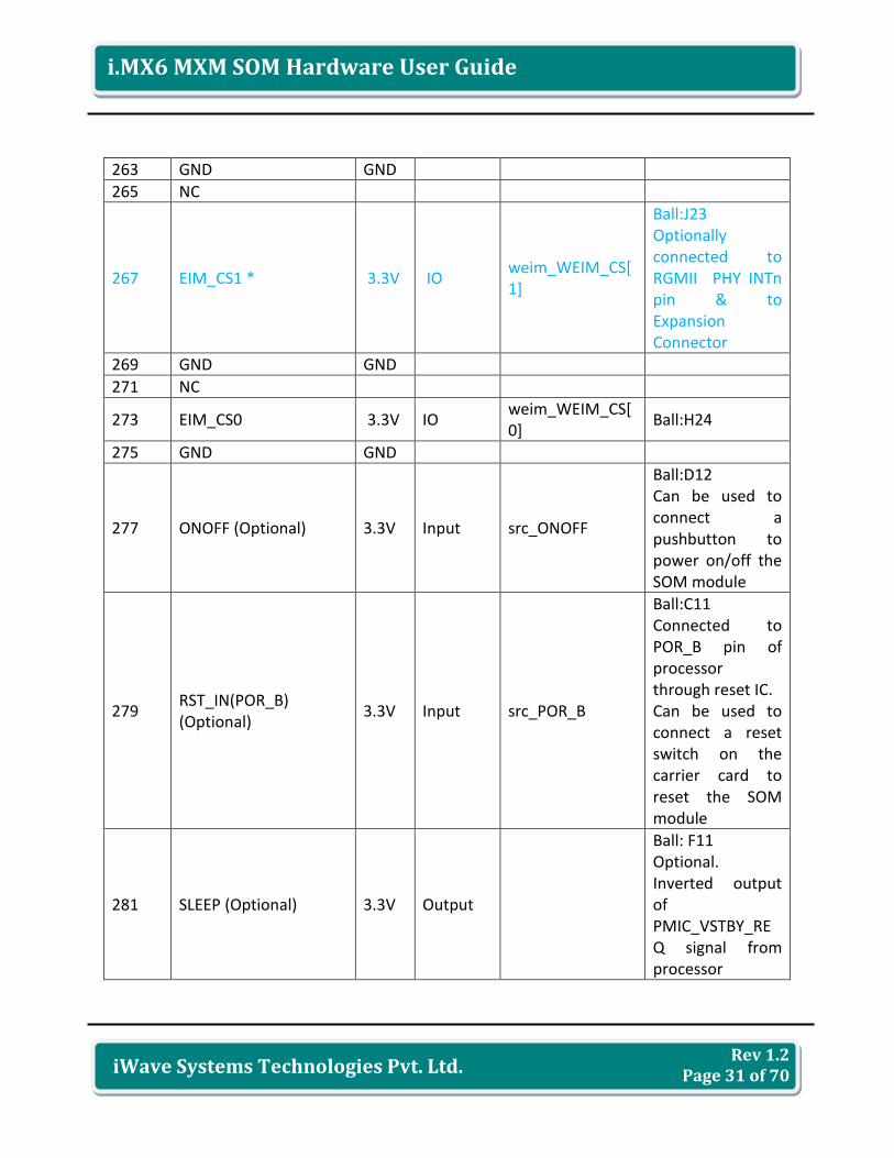
Rev 1.2 Page 31 of 70
i.MX6 MXM SOM Hardware User Guide
iWave Systems Technologies Pvt. Ltd.
263 GND GND
265 NC
267 EIM_CS1 * 3.3V IO weim_WEIM_CS[1]
Ball:J23 Optionally connected to RGMII PHY INTn pin & to Expansion Connector
269 GND GND
271 NC
273 EIM_CS0 3.3V IO weim_WEIM_CS[0]
Ball:H24
275 GND GND
277 ONOFF (Optional) 3.3V Input src_ONOFF
Ball:D12 Can be used to connect a pushbutton to power on/off the SOM module
279 RST_IN(POR_B) (Optional)
3.3V Input src_POR_B
Ball:C11 Connected to POR_B pin of processor through reset IC. Can be used to connect a reset switch on the carrier card to reset the SOM module
281 SLEEP (Optional) 3.3V Output
Ball: F11 Optional. Inverted output of PMIC_VSTBY_REQ signal from processor
Rev 1.2 Page 32 of 70
i.MX6 MXM SOM Hardware User Guide
iWave Systems Technologies Pvt. Ltd.
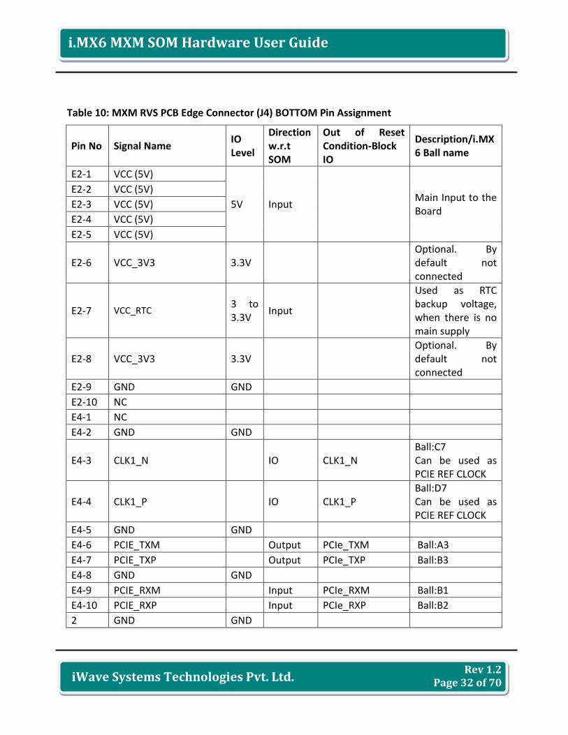
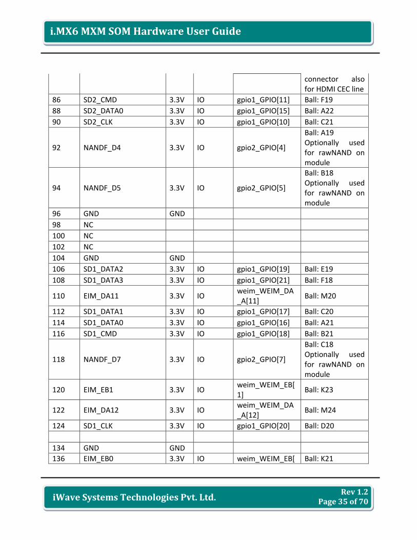
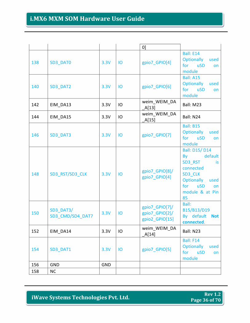
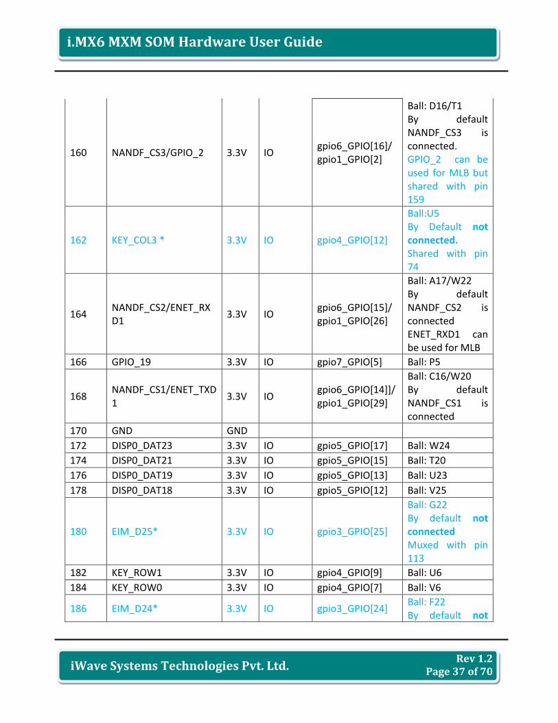
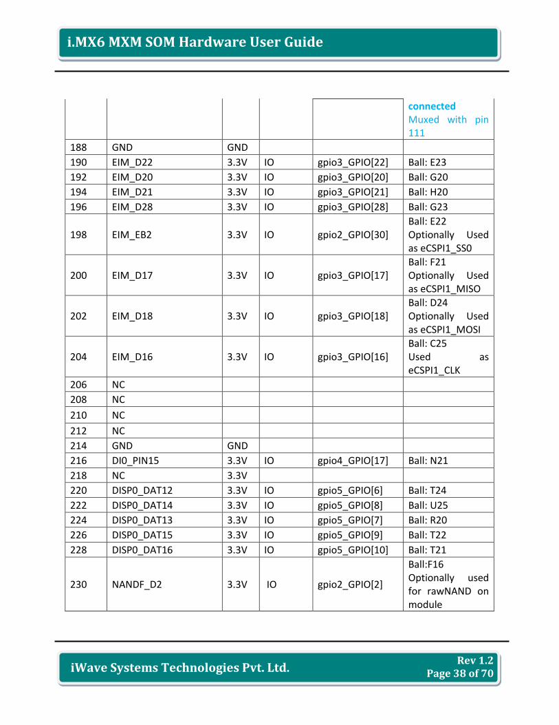
Table 10: MXM RVS PCB Edge Connector (J4) BOTTOM Pin Assignment
Pin No Signal Name IO Level
Direction w.r.t SOM
Out of Reset Condition-Block IO
Description/i.MX6 Ball name
E2-1 VCC (5V)
5V Input Main Input to the Board
E2-2 VCC (5V)
E2-3 VCC (5V)
E2-4 VCC (5V)
E2-5 VCC (5V)
E2-6 VCC_3V3 3.3V
Optional. By default not connected
E2-7 VCC_RTC 3 to 3.3V
Input
Used as RTC backup voltage, when there is no main supply
E2-8 VCC_3V3 3.3V
Optional. By default not connected
E2-9 GND GND
E2-10 NC
E4-1 NC
E4-2 GND GND
E4-3 CLK1_N
IO CLK1_N Ball:C7 Can be used as PCIE REF CLOCK
E4-4 CLK1_P
IO CLK1_P Ball:D7 Can be used as PCIE REF CLOCK
E4-5 GND GND
E4-6 PCIE_TXM
Output PCIe_TXM Ball:A3
E4-7 PCIE_TXP
Output PCIe_TXP Ball:B3
E4-8 GND GND
E4-9 PCIE_RXM
Input PCIe_RXM Ball:B1
E4-10 PCIE_RXP
Input PCIe_RXP Ball:B2
2 GND GND
Rev 1.2 Page 33 of 70
i.MX6 MXM SOM Hardware User Guide
iWave Systems Technologies Pvt. Ltd.
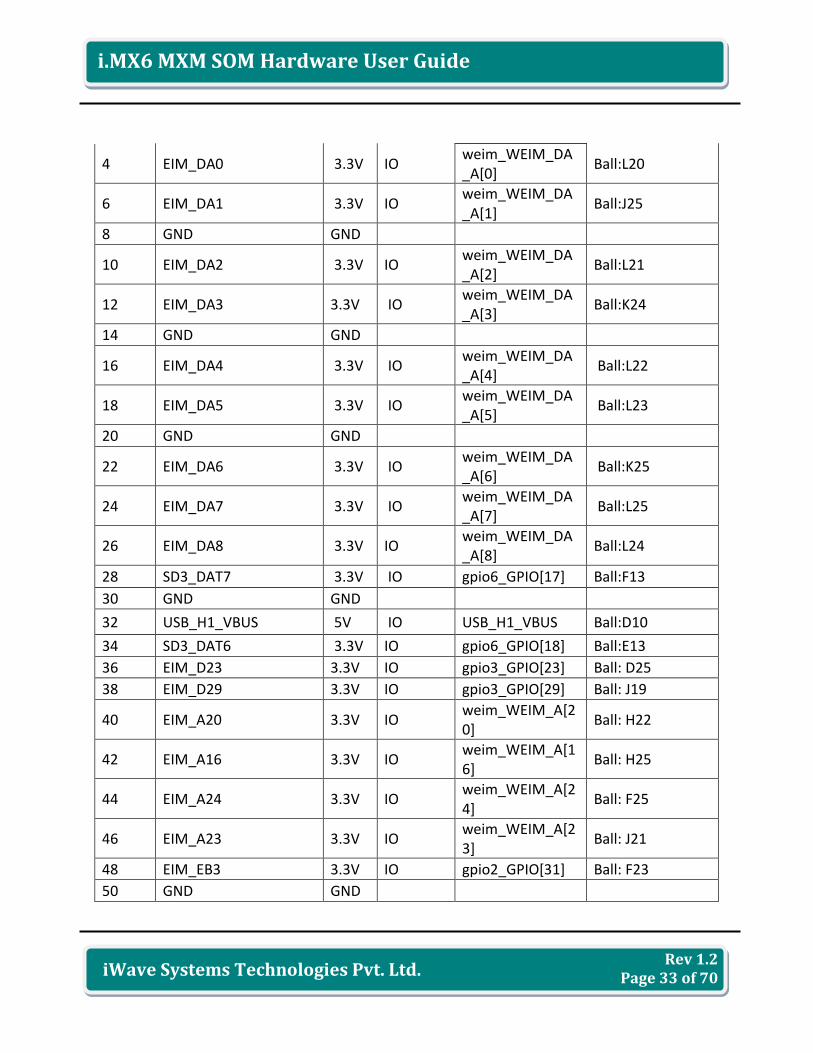
4 EIM_DA0 3.3V IO weim_WEIM_DA_A[0]
Ball:L20
6 EIM_DA1 3.3V IO weim_WEIM_DA_A[1]
Ball:J25
8 GND GND
10 EIM_DA2 3.3V IO weim_WEIM_DA_A[2]
Ball:L21
12 EIM_DA3 3.3V IO weim_WEIM_DA_A[3]
Ball:K24
14 GND GND
16 EIM_DA4 3.3V IO weim_WEIM_DA_A[4]
Ball:L22
18 EIM_DA5 3.3V IO weim_WEIM_DA_A[5]
Ball:L23
20 GND GND
22 EIM_DA6 3.3V IO weim_WEIM_DA_A[6]
Ball:K25
24 EIM_DA7 3.3V IO weim_WEIM_DA_A[7]
Ball:L25
26 EIM_DA8 3.3V IO weim_WEIM_DA_A[8]
Ball:L24
28 SD3_DAT7 3.3V IO gpio6_GPIO[17] Ball:F13
30 GND GND
32 USB_H1_VBUS 5V IO USB_H1_VBUS Ball:D10
34 SD3_DAT6 3.3V IO gpio6_GPIO[18] Ball:E13
36 EIM_D23 3.3V IO gpio3_GPIO[23] Ball: D25
38 EIM_D29 3.3V IO gpio3_GPIO[29] Ball: J19
40 EIM_A20 3.3V IO weim_WEIM_A[20]
Ball: H22
42 EIM_A16 3.3V IO weim_WEIM_A[16]
Ball: H25
44 EIM_A24 3.3V IO weim_WEIM_A[24]
Ball: F25
46 EIM_A23 3.3V IO weim_WEIM_A[23]
Ball: J21
48 EIM_EB3 3.3V IO gpio2_GPIO[31] Ball: F23
50 GND GND
Rev 1.2 Page 34 of 70
i.MX6 MXM SOM Hardware User Guide
iWave Systems Technologies Pvt. Ltd.
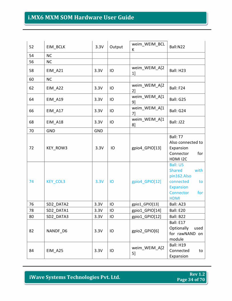
52 EIM_BCLK 3.3V Output weim_WEIM_BCLK
Ball:N22
54 NC
56 NC
58 EIM_A21 3.3V IO weim_WEIM_A[21]
Ball: H23
60 NC
62 EIM_A22 3.3V IO weim_WEIM_A[22]
Ball: F24
64 EIM_A19 3.3V IO weim_WEIM_A[19]
Ball: G25
66 EIM_A17 3.3V IO weim_WEIM_A[17]
Ball: G24
68 EIM_A18 3.3V IO weim_WEIM_A[18]
Ball: J22
70 GND GND
72 KEY_ROW3 3.3V IO gpio4_GPIO[13]
Ball: T7 Also connected to Expansion Connector for HDMI I2C
74 KEY_COL3 3.3V IO gpio4_GPIO[12]
Ball: U5 Shared with pin162.Also connected to Expansion Connector for HDMI
76 SD2_DATA2 3.3V IO gpio1_GPIO[13] Ball: A23
78 SD2_DATA1 3.3V IO gpio1_GPIO[14] Ball: E20
80 SD2_DATA3 3.3V IO gpio1_GPIO[12] Ball: B22
82 NANDF_D6 3.3V IO gpio2_GPIO[6]
Ball: E17 Optionally used for rawNAND on module
84 EIM_A25 3.3V IO weim_WEIM_A[25]
Ball: H19 Connected to Expansion
Rev 1.2 Page 35 of 70
i.MX6 MXM SOM Hardware User Guide
iWave Systems Technologies Pvt. Ltd.
connector also for HDMI CEC line
86 SD2_CMD 3.3V IO gpio1_GPIO[11] Ball: F19
88 SD2_DATA0 3.3V IO gpio1_GPIO[15] Ball: A22
90 SD2_CLK 3.3V IO gpio1_GPIO[10] Ball: C21
92 NANDF_D4 3.3V IO gpio2_GPIO[4]
Ball: A19 Optionally used for rawNAND on module
94 NANDF_D5 3.3V IO gpio2_GPIO[5]
Ball: B18 Optionally used for rawNAND on module
96 GND GND
98 NC
100 NC
102 NC
104 GND GND
106 SD1_DATA2 3.3V IO gpio1_GPIO[19] Ball: E19
108 SD1_DATA3 3.3V IO gpio1_GPIO[21] Ball: F18
110 EIM_DA11 3.3V IO weim_WEIM_DA_A[11]
Ball: M20
112 SD1_DATA1 3.3V IO gpio1_GPIO[17] Ball: C20
114 SD1_DATA0 3.3V IO gpio1_GPIO[16] Ball: A21
116 SD1_CMD 3.3V IO gpio1_GPIO[18] Ball: B21
118 NANDF_D7 3.3V IO gpio2_GPIO[7]
Ball: C18 Optionally used for rawNAND on module
120 EIM_EB1 3.3V IO weim_WEIM_EB[1]
Ball: K23
122 EIM_DA12 3.3V IO weim_WEIM_DA_A[12]
Ball: M24
124 SD1_CLK 3.3V IO gpio1_GPIO[20] Ball: D20
134 GND GND
136 EIM_EB0 3.3V IO weim_WEIM_EB[ Ball: K21
Rev 1.2 Page 36 of 70
i.MX6 MXM SOM Hardware User Guide
iWave Systems Technologies Pvt. Ltd.
0]
138 SD3_DAT0 3.3V IO gpio7_GPIO[4]
Ball: E14 Optionally used for uSD on module
140 SD3_DAT2 3.3V IO gpio7_GPIO[6]
Ball: A15 Optionally used for uSD on module
142 EIM_DA13 3.3V IO weim_WEIM_DA_A[13]
Ball: M23
144 EIM_DA15 3.3V IO weim_WEIM_DA_A[15]
Ball: N24
146 SD3_DAT3 3.3V IO gpio7_GPIO[7]
Ball: B15 Optionally used for uSD on module
148 SD3_RST/SD3_CLK 3.3V IO gpio7_GPIO[8]/ gpio7_GPIO[4]
Ball: D15/ D14 By default SD3_RST is connected SD3_CLK Optionally used for uSD on module & at Pin 85
150 SD3_DAT3/ SD3_CMD/SD4_DAT7
3.3V IO gpio7_GPIO[7]/ gpio7_GPIO[2]/ gpio2_GPIO[15]
Ball: B15/B13/D19 By default Not connected.
152 EIM_DA14 3.3V IO weim_WEIM_DA_A[14]
Ball: N23
154 SD3_DAT1 3.3V IO gpio7_GPIO[5]
Ball: F14 Optionally used for uSD on module
156 GND GND
158 NC
Rev 1.2 Page 37 of 70
i.MX6 MXM SOM Hardware User Guide
iWave Systems Technologies Pvt. Ltd.
160 NANDF_CS3/GPIO_2 3.3V IO gpio6_GPIO[16]/ gpio1_GPIO[2]
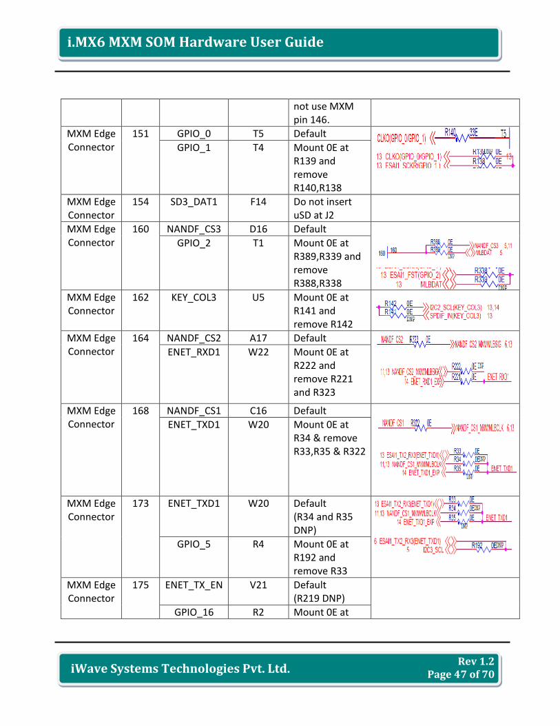
Ball: D16/T1 By default NANDF_CS3 is connected. GPIO_2 can be used for MLB but shared with pin 159
162 KEY_COL3 * 3.3V IO gpio4_GPIO[12]
Ball:U5 By Default not connected. Shared with pin 74
164 NANDF_CS2/ENET_RXD1
3.3V IO gpio6_GPIO[15]/ gpio1_GPIO[26]
Ball: A17/W22 By default NANDF_CS2 is connected ENET_RXD1 can be used for MLB
166 GPIO_19 3.3V IO gpio7_GPIO[5] Ball: P5
168 NANDF_CS1/ENET_TXD1
3.3V IO gpio6_GPIO[14]]/ gpio1_GPIO[29]
Ball: C16/W20 By default NANDF_CS1 is connected
170 GND GND
172 DISP0_DAT23 3.3V IO gpio5_GPIO[17] Ball: W24
174 DISP0_DAT21 3.3V IO gpio5_GPIO[15] Ball: T20
176 DISP0_DAT19 3.3V IO gpio5_GPIO[13] Ball: U23
178 DISP0_DAT18 3.3V IO gpio5_GPIO[12] Ball: V25
180 EIM_D25* 3.3V IO gpio3_GPIO[25]
Ball: G22 By default not connected Muxed with pin 113
182 KEY_ROW1 3.3V IO gpio4_GPIO[9] Ball: U6
184 KEY_ROW0 3.3V IO gpio4_GPIO[7] Ball: V6
186 EIM_D24* 3.3V IO gpio3_GPIO[24] Ball: F22 By default not
Rev 1.2 Page 38 of 70
i.MX6 MXM SOM Hardware User Guide
iWave Systems Technologies Pvt. Ltd.
connected Muxed with pin 111
188 GND GND
190 EIM_D22 3.3V IO gpio3_GPIO[22] Ball: E23
192 EIM_D20 3.3V IO gpio3_GPIO[20] Ball: G20
194 EIM_D21 3.3V IO gpio3_GPIO[21] Ball: H20
196 EIM_D28 3.3V IO gpio3_GPIO[28] Ball: G23
198 EIM_EB2 3.3V IO gpio2_GPIO[30] Ball: E22 Optionally Used as eCSPI1_SS0
200 EIM_D17 3.3V IO gpio3_GPIO[17] Ball: F21 Optionally Used as eCSPI1_MISO
202 EIM_D18 3.3V IO gpio3_GPIO[18] Ball: D24 Optionally Used as eCSPI1_MOSI
204 EIM_D16 3.3V IO gpio3_GPIO[16] Ball: C25 Used as eCSPI1_CLK
206 NC
208 NC
210 NC
212 NC
214 GND GND
216 DI0_PIN15 3.3V IO gpio4_GPIO[17] Ball: N21
218 NC 3.3V
220 DISP0_DAT12 3.3V IO gpio5_GPIO[6] Ball: T24
222 DISP0_DAT14 3.3V IO gpio5_GPIO[8] Ball: U25
224 DISP0_DAT13 3.3V IO gpio5_GPIO[7] Ball: R20
226 DISP0_DAT15 3.3V IO gpio5_GPIO[9] Ball: T22
228 DISP0_DAT16 3.3V IO gpio5_GPIO[10] Ball: T21
230 NANDF_D2 3.3V IO gpio2_GPIO[2]
Ball:F16 Optionally used for rawNAND on module
Rev 1.2 Page 39 of 70
i.MX6 MXM SOM Hardware User Guide
iWave Systems Technologies Pvt. Ltd.
232 DI0_DISP_CLK 3.3V IO gpio4_GPIO[16] Ball: N19
234 DISP0_DAT17 3.3V IO gpio5_GPIO[11] Ball: U24
236 GND GND
238 GPHY_DTXRXP(NC) 3.3V IO
Gigabit Eth PHY output. Used only for 1000Base-T Mode
240 GPHY_DTXRXM(NC) 3.3V IO
Gigabit Eth PHY output. Used only for 1000Base-T Mode
242 CSI0_DAT8 3.3V IO gpio5_GPIO[26] Ball: N6 I2C1 Data signal
244 CSI0_DAT9 3.3V IO gpio5_GPIO[27] Ball: N5 I2C1 Clock signal
246 GPIO_16 3.3V IO gpio7_GPIO[11]
Ball: R2 I2C3 Data signal Optionally Shared with Pin175
248 GPIO_5 3.3V IO gpio1_GPIO[5]
Ball: R4 I2C3 Clock signal Optionally Shared with Pin173
250 GND GND
252 NC
254 EIM_D19 3.3V IO gpio3_GPIO[19] Ball:G21 Optionally Used as eCSPI1_SS1
256 NC
258 LED1 (NC) 3.3V Output
Gigabit Eth PHY Link activity LED Indication. Active low
Rev 1.2 Page 40 of 70
i.MX6 MXM SOM Hardware User Guide
iWave Systems Technologies Pvt. Ltd.
260 LED2(NC) 3.3V Output
Gigabit Eth PHY Link Speed LED Indication. Active low
262 GPHY_CTXRXP(NC) 3.3V IO
Gigabit Eth PHY output. Used only for 1000Base-T Mode
264 GPHY_CTXRXM(NC) 3.3V IO
Gigabit Eth PHY output. Used only for 1000Base-T Mode
266 GND GND
268 GPHY_BTXRXP(NC) 3.3V Input
Gigabit Eth PHY output. Used for 10Base-T / 100Base-TX/ 1000Base-T Mode
270 GPHY_BTXRXM(NC) 3.3V Input
Gigabit Eth PHY output. Used for 10Base-T / 100Base-TX/ 1000Base-T Mode
272 GPHY_ATXRXP(NC) 3.3V Output
Gigabit Eth PHY output. Used for 10Base-T / 100Base-TX/ 1000Base-T Mode
274 GPHY_ATXRXM(NC) 3.3V Output
Gigabit Eth PHY output. Used for 10Base-T / 100Base-TX/ 1000Base-T
Rev 1.2 Page 41 of 70
i.MX6 MXM SOM Hardware User Guide
iWave Systems Technologies Pvt. Ltd.
Mode
276 GND GND
278 EIM_LBA 3.3V IO weim_WEIM_LBA
Ball: K22 Optionally used for Ethernet PHy reset. Also connected to Expansion connector
280 PWR_RDY 3.3V Output
Power Ready signal of SOM. Pull up to last supply on SOM(3.3V) Used for power on sequencing of carrier board
Rev 1.2 Page 42 of 70
i.MX6 MXM SOM Hardware User Guide
iWave Systems Technologies Pvt. Ltd.
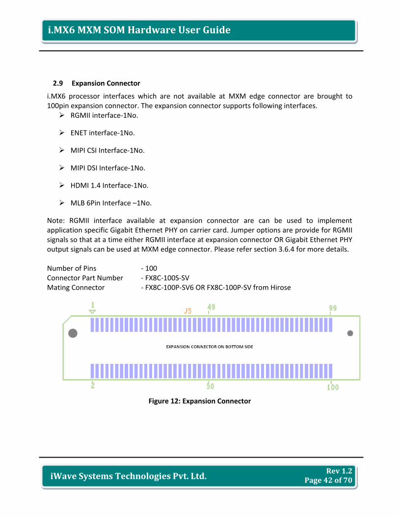
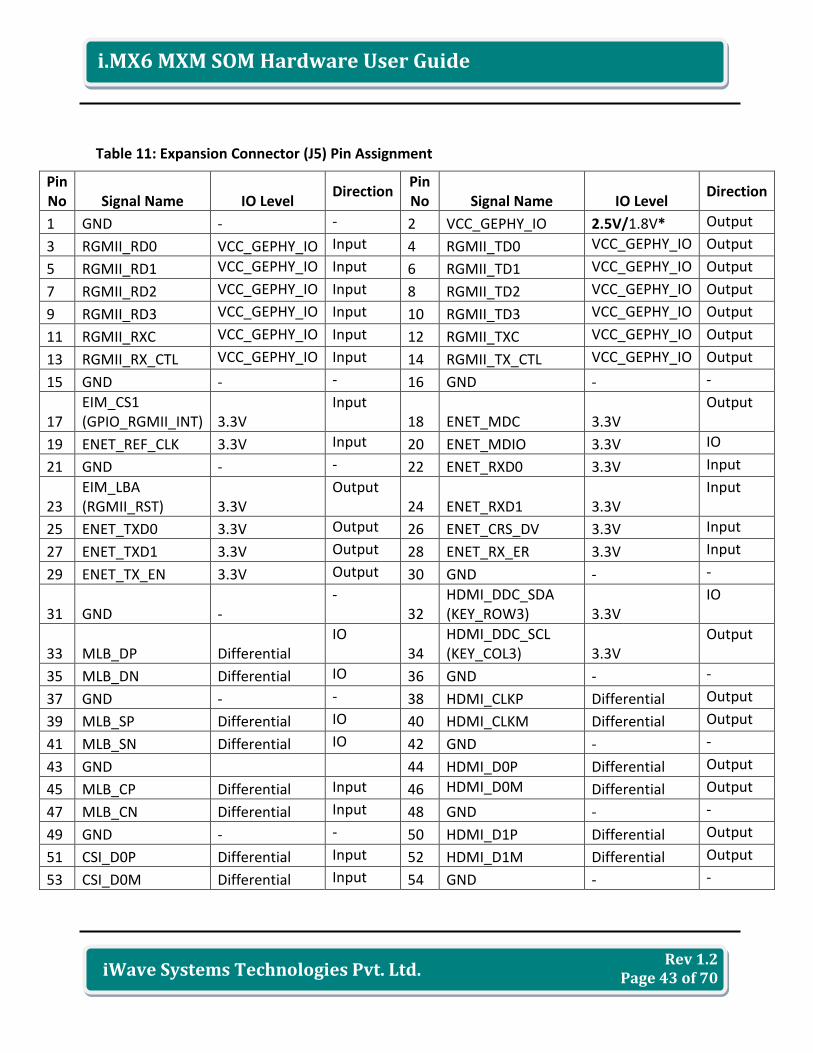
2.9 Expansion Connector
i.MX6 processor interfaces which are not available at MXM edge connector are brought to 100pin expansion connector. The expansion connector supports following interfaces. RGMII interface-1No.
ENET interface-1No.
MIPI CSI Interface-1No.
MIPI DSI Interface-1No.
HDMI 1.4 Interface-1No.
MLB 6Pin Interface –1No.
Note: RGMII interface available at expansion connector are can be used to implement application specific Gigabit Ethernet PHY on carrier card. Jumper options are provide for RGMII signals so that at a time either RGMII interface at expansion connector OR Gigabit Ethernet PHY output signals can be used at MXM edge connector. Please refer section 3.6.4 for more details. Number of Pins - 100 Connector Part Number - FX8C-100S-SV Mating Connector - FX8C-100P-SV6 OR FX8C-100P-SV from Hirose
Figure 12: Expansion Connector
Rev 1.2 Page 43 of 70
i.MX6 MXM SOM Hardware User Guide
iWave Systems Technologies Pvt. Ltd.
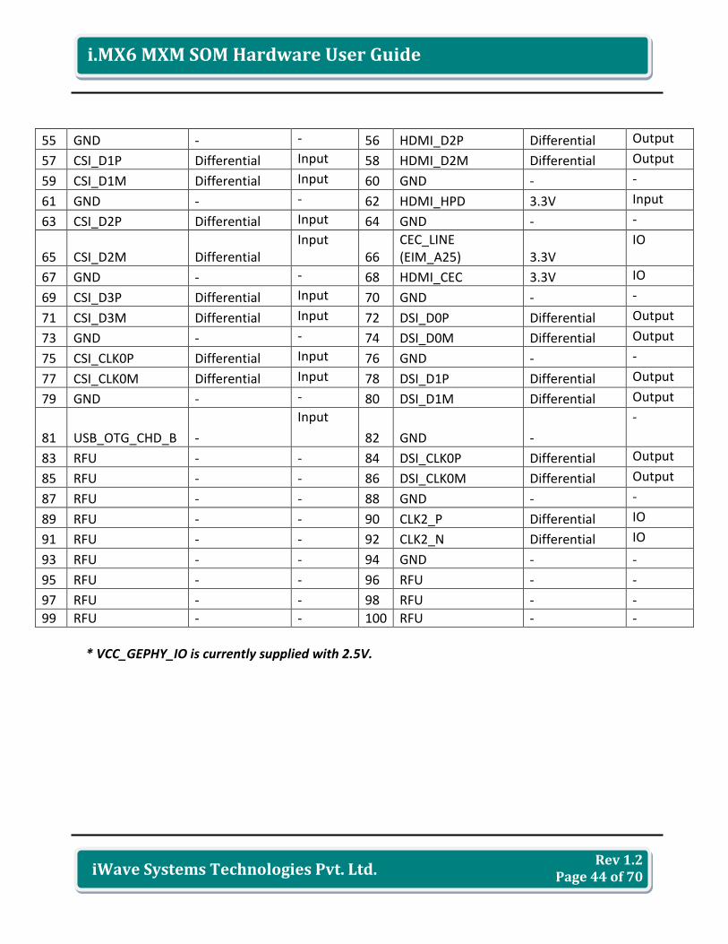
Table 11: Expansion Connector (J5) Pin Assignment
Pin No Signal Name IO Level
Direction Pin No Signal Name IO Level
Direction
1 GND - - 2 VCC_GEPHY_IO 2.5V/1.8V* Output
3 RGMII_RD0 VCC_GEPHY_IO Input 4 RGMII_TD0 VCC_GEPHY_IO Output
5 RGMII_RD1 VCC_GEPHY_IO Input 6 RGMII_TD1 VCC_GEPHY_IO Output
7 RGMII_RD2 VCC_GEPHY_IO Input 8 RGMII_TD2 VCC_GEPHY_IO Output
9 RGMII_RD3 VCC_GEPHY_IO Input 10 RGMII_TD3 VCC_GEPHY_IO Output
11 RGMII_RXC VCC_GEPHY_IO Input 12 RGMII_TXC VCC_GEPHY_IO Output
13 RGMII_RX_CTL VCC_GEPHY_IO Input 14 RGMII_TX_CTL VCC_GEPHY_IO Output
15 GND - - 16 GND - -
17 EIM_CS1 (GPIO_RGMII_INT) 3.3V
Input 18 ENET_MDC 3.3V
Output
19 ENET_REF_CLK 3.3V Input 20 ENET_MDIO 3.3V IO
21 GND - - 22 ENET_RXD0 3.3V Input
23 EIM_LBA (RGMII_RST) 3.3V
Output 24 ENET_RXD1 3.3V
Input
25 ENET_TXD0 3.3V Output 26 ENET_CRS_DV 3.3V Input
27 ENET_TXD1 3.3V Output 28 ENET_RX_ER 3.3V Input
29 ENET_TX_EN 3.3V Output 30 GND - -
31 GND - -
32 HDMI_DDC_SDA (KEY_ROW3) 3.3V
IO
33 MLB_DP Differential IO
34 HDMI_DDC_SCL (KEY_COL3) 3.3V
Output
35 MLB_DN Differential IO 36 GND - -
37 GND - - 38 HDMI_CLKP Differential Output
39 MLB_SP Differential IO 40 HDMI_CLKM Differential Output
41 MLB_SN Differential IO 42 GND - -
43 GND
44 HDMI_D0P Differential Output
45 MLB_CP Differential Input 46 HDMI_D0M Differential Output
47 MLB_CN Differential Input 48 GND - -
49 GND - - 50 HDMI_D1P Differential Output
51 CSI_D0P Differential Input 52 HDMI_D1M Differential Output
53 CSI_D0M Differential Input 54 GND - -
Rev 1.2 Page 44 of 70
i.MX6 MXM SOM Hardware User Guide
iWave Systems Technologies Pvt. Ltd.
55 GND - - 56 HDMI_D2P Differential Output
57 CSI_D1P Differential Input 58 HDMI_D2M Differential Output
59 CSI_D1M Differential Input 60 GND - -
61 GND - - 62 HDMI_HPD 3.3V Input
63 CSI_D2P Differential Input 64 GND - -
65 CSI_D2M Differential Input
66 CEC_LINE (EIM_A25) 3.3V
IO
67 GND - - 68 HDMI_CEC 3.3V IO
69 CSI_D3P Differential Input 70 GND - -
71 CSI_D3M Differential Input 72 DSI_D0P Differential Output
73 GND - - 74 DSI_D0M Differential Output
75 CSI_CLK0P Differential Input 76 GND - -
77 CSI_CLK0M Differential Input 78 DSI_D1P Differential Output
79 GND - - 80 DSI_D1M Differential Output
81 USB_OTG_CHD_B -
Input
82 GND -
-
83 RFU - - 84 DSI_CLK0P Differential Output
85 RFU - - 86 DSI_CLK0M Differential Output
87 RFU - - 88 GND - -
89 RFU - - 90 CLK2_P Differential IO
91 RFU - - 92 CLK2_N Differential IO
93 RFU - - 94 GND - -
95 RFU - - 96 RFU - -
97 RFU - - 98 RFU - -
99 RFU - - 100 RFU - -
* VCC_GEPHY_IO is currently supplied with 2.5V.
Rev 1.2 Page 45 of 70
i.MX6 MXM SOM Hardware User Guide
iWave Systems Technologies Pvt. Ltd.
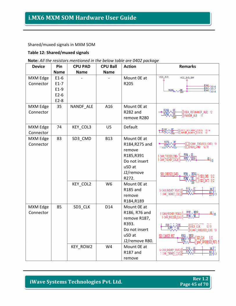
Shared/muxed signals in MXM SOM
Table 12: Shared/muxed signals
Note: All the resistors mentioned in the below table are 0402 package
Device Pin Name
CPU PAD Name
CPU Ball Name
Action Remarks
MXM Edge Connector
E1-6 E1-7 E1-9 E2-6 E2-8
- - Mount 0E at R205
MXM Edge Connector
35 NANDF_ALE A16 Mount 0E at R282 and remove R280
MXM Edge Connector
74 KEY_COL3 U5 Default
MXM Edge Connector
83 SD3_CMD B13 Mount 0E at R184,R275 and remove R185,R391 Do not insert uSD at J2/remove R272.
KEY_COL2 W6 Mount 0E at R185 and remove R184,R189
MXM Edge Connector
85 SD3_CLK D14 Mount 0E at R186, R76 and remove R187, R393. Do not insert uSD at J2/remove R80.
KEY_ROW2 W4 Mount 0E at R187 and remove
Rev 1.2 Page 46 of 70
i.MX6 MXM SOM Hardware User Guide
iWave Systems Technologies Pvt. Ltd.
R186,R188
MXM Edge Connector
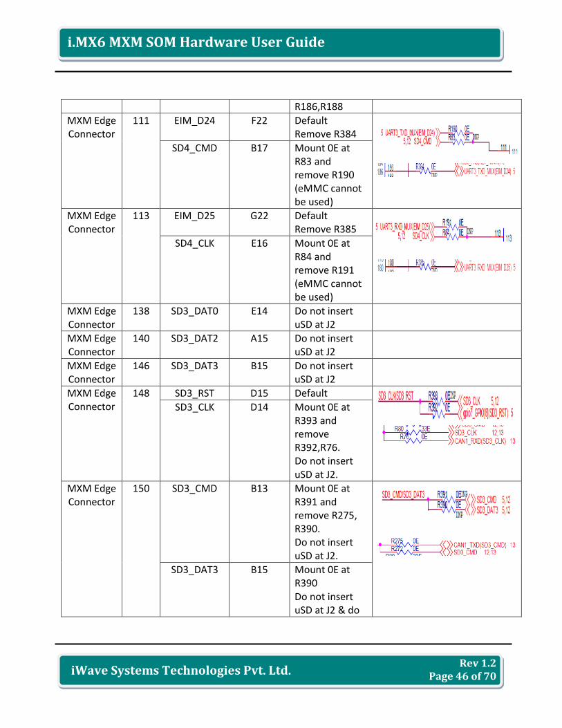
111 EIM_D24 F22 Default Remove R384
SD4_CMD B17 Mount 0E at R83 and remove R190 (eMMC cannot be used)
MXM Edge Connector
113 EIM_D25 G22 Default Remove R385
SD4_CLK E16 Mount 0E at R84 and remove R191 (eMMC cannot be used)
MXM Edge Connector
138 SD3_DAT0 E14 Do not insert uSD at J2
MXM Edge Connector
140 SD3_DAT2 A15 Do not insert uSD at J2
MXM Edge Connector
146 SD3_DAT3 B15 Do not insert uSD at J2
MXM Edge Connector
148 SD3_RST D15 Default
SD3_CLK D14 Mount 0E at R393 and remove R392,R76. Do not insert uSD at J2.
MXM Edge Connector
150 SD3_CMD B13 Mount 0E at R391 and remove R275, R390. Do not insert uSD at J2.
SD3_DAT3 B15 Mount 0E at R390 Do not insert uSD at J2 & do
Rev 1.2 Page 47 of 70
i.MX6 MXM SOM Hardware User Guide
iWave Systems Technologies Pvt. Ltd.
not use MXM pin 146.
MXM Edge Connector
151 GPIO_0 T5 Default
GPIO_1 T4 Mount 0E at R139 and remove R140,R138
MXM Edge Connector
154 SD3_DAT1 F14 Do not insert uSD at J2
MXM Edge Connector
160 NANDF_CS3 D16 Default
GPIO_2 T1 Mount 0E at R389,R339 and remove R388,R338
MXM Edge Connector
162 KEY_COL3 U5 Mount 0E at R141 and remove R142
MXM Edge Connector
164 NANDF_CS2 A17 Default
ENET_RXD1 W22 Mount 0E at R222 and remove R221 and R323
MXM Edge Connector
168 NANDF_CS1 C16 Default
ENET_TXD1 W20 Mount 0E at R34 & remove R33,R35 & R322
MXM Edge Connector
173 ENET_TXD1 W20 Default (R34 and R35 DNP)
GPIO_5 R4 Mount 0E at R192 and remove R33
MXM Edge Connector
175 ENET_TX_EN V21 Default (R219 DNP)
GPIO_16 R2 Mount 0E at
Rev 1.2 Page 48 of 70
i.MX6 MXM SOM Hardware User Guide
iWave Systems Technologies Pvt. Ltd.
R193 and remove R220
MXM Edge Connector
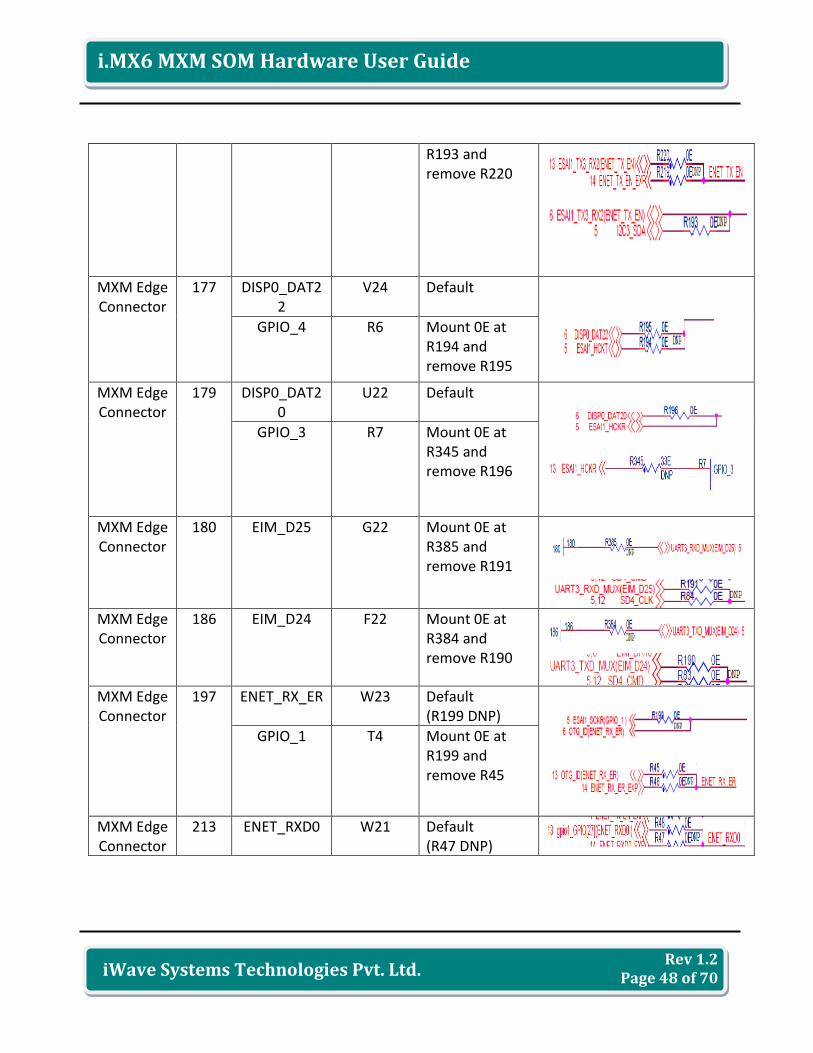
177 DISP0_DAT22
V24 Default
GPIO_4 R6 Mount 0E at R194 and remove R195
MXM Edge Connector
179 DISP0_DAT20
U22 Default
GPIO_3 R7 Mount 0E at R345 and remove R196
MXM Edge Connector
180 EIM_D25 G22 Mount 0E at R385 and remove R191
MXM Edge Connector
186 EIM_D24 F22 Mount 0E at R384 and remove R190
MXM Edge Connector
197 ENET_RX_ER
W23 Default (R199 DNP)
GPIO_1 T4 Mount 0E at R199 and remove R45
MXM Edge Connector
213 ENET_RXD0 W21 Default (R47 DNP)
Rev 1.2 Page 49 of 70
i.MX6 MXM SOM Hardware User Guide
iWave Systems Technologies Pvt. Ltd.
MXM Edge Connector
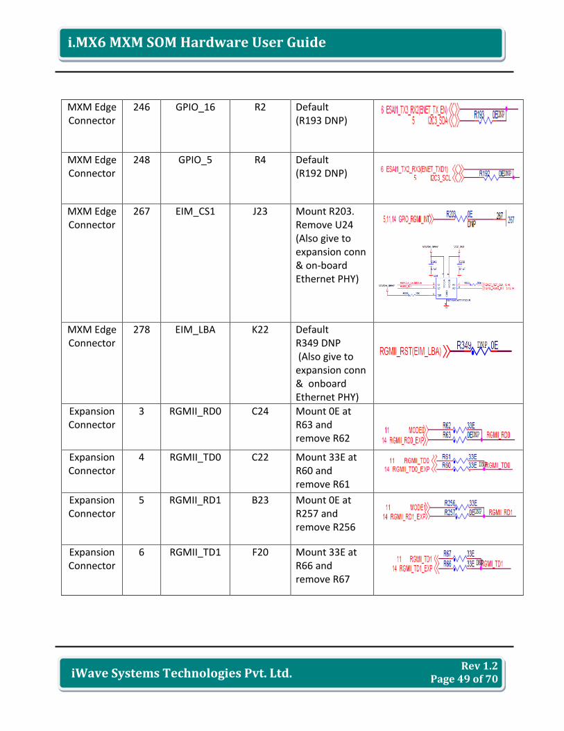
246 GPIO_16 R2 Default (R193 DNP)
MXM Edge Connector
248 GPIO_5 R4 Default (R192 DNP)
MXM Edge Connector
267 EIM_CS1 J23 Mount R203. Remove U24 (Also give to expansion conn & on-board Ethernet PHY)
MXM Edge Connector
278 EIM_LBA K22 Default R349 DNP (Also give to expansion conn & onboard Ethernet PHY)
Expansion Connector
3 RGMII_RD0 C24 Mount 0E at R63 and remove R62
Expansion Connector
4 RGMII_TD0 C22 Mount 33E at R60 and remove R61
Expansion Connector
5 RGMII_RD1 B23 Mount 0E at R257 and remove R256
Expansion Connector
6 RGMII_TD1 F20 Mount 33E at R66 and remove R67
Rev 1.2 Page 50 of 70
i.MX6 MXM SOM Hardware User Guide
iWave Systems Technologies Pvt. Ltd.
Expansion Connector
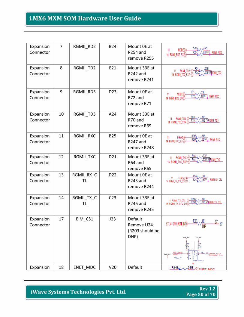
7 RGMII_RD2 B24 Mount 0E at R254 and remove R255
Expansion Connector
8 RGMII_TD2 E21 Mount 33E at R242 and remove R241
Expansion Connector
9 RGMII_RD3 D23 Mount 0E at R72 and remove R71
Expansion Connector
10 RGMII_TD3 A24 Mount 33E at R70 and remove R69
Expansion Connector
11 RGMII_RXC B25 Mount 0E at R247 and remove R248
Expansion Connector
12 RGMII_TXC D21 Mount 33E at R64 and remove R65
Expansion Connector
13 RGMII_RX_CTL
D22 Mount 0E at R243 and remove R244
Expansion Connector
14 RGMII_TX_CTL
C23 Mount 33E at R246 and remove R245
Expansion Connector
17 EIM_CS1 J23 Default Remove U24. (R203 should be DNP)
Expansion 18 ENET_MDC V20 Default
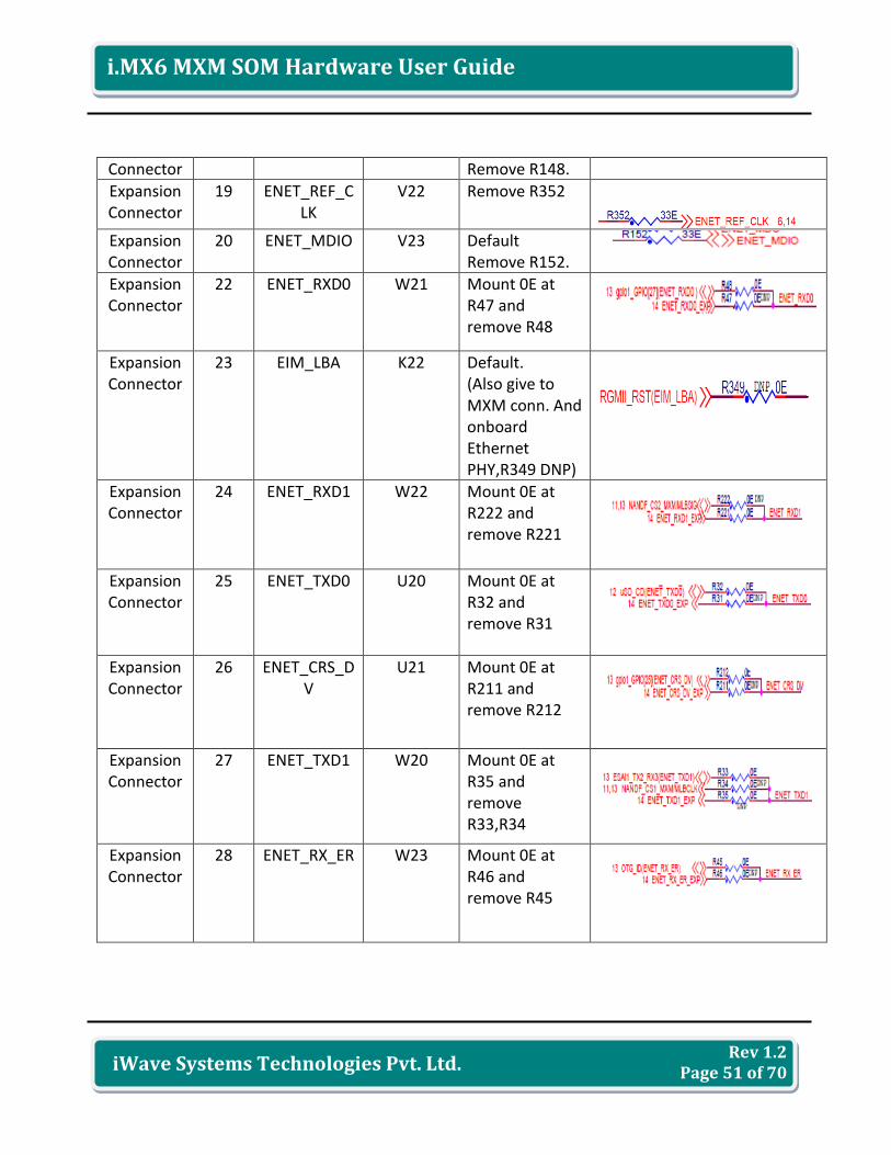
Rev 1.2 Page 51 of 70
i.MX6 MXM SOM Hardware User Guide
iWave Systems Technologies Pvt. Ltd.
Connector Remove R148.
Expansion Connector
19 ENET_REF_CLK
V22 Remove R352
Expansion Connector
20 ENET_MDIO V23 Default Remove R152.
Expansion Connector
22 ENET_RXD0 W21 Mount 0E at R47 and remove R48
Expansion Connector
23 EIM_LBA K22 Default. (Also give to MXM conn. And onboard Ethernet PHY,R349 DNP)
Expansion Connector
24 ENET_RXD1 W22 Mount 0E at R222 and remove R221
Expansion Connector
25 ENET_TXD0 U20 Mount 0E at R32 and remove R31
Expansion Connector
26 ENET_CRS_DV
U21 Mount 0E at R211 and remove R212
Expansion Connector
27 ENET_TXD1 W20 Mount 0E at R35 and remove R33,R34
Expansion Connector
28 ENET_RX_ER W23 Mount 0E at R46 and remove R45

Rev 1.2 Page 52 of 70
i.MX6 MXM SOM Hardware User Guide
iWave Systems Technologies Pvt. Ltd.
Expansion Connector
29 ENET_TX_EN V21 Mount 0E at R219 and remove R220

Rev 1.2 Page 53 of 70
i.MX6 MXM SOM Hardware User Guide
iWave Systems Technologies Pvt. Ltd.
3. i.M6 MXM SOM USAGE REQUIREMENT
This chapter deals with the power supply requirement, sequencing & other details about specific interfaces that need to be taken care while designing carrier card for i.MX6 MXM SOM.
3.1 Power Supply Requirement
i.MX6 MXM SOM will work with 5V power input from MXM Edge connector or through power connector (P1). Power connector P1 is the optional feature and will not be populated in default configuration & used only for initial stand alone testing of i.MX6 MXM SOM.
Figure 13: 2Pin Power connector
Table 13: 2pin Power Connector
Pin No
Signals Input/ Output
Voltage Level Description
1 VCC_IN Power 5V +/- 5% 5V Input Power
2 GND Power GND Ground
3.2 Power Consumption
i.MX6 MXM SOM typical power consumption is 5W. ie 1A @ 5V Note that this power consumption was noted during RAM read/write test at u-boot level with 4nos of 2Gbit DDR3 chips & 4GB eMMC chip SOM configuration.
Number of Pins (P1) - 2 Connector Part Number - 0099990986 Mating Connector - 22-43-3020 from Molex
Rev 1.2 Page 54 of 70
i.MX6 MXM SOM Hardware User Guide
iWave Systems Technologies Pvt. Ltd.
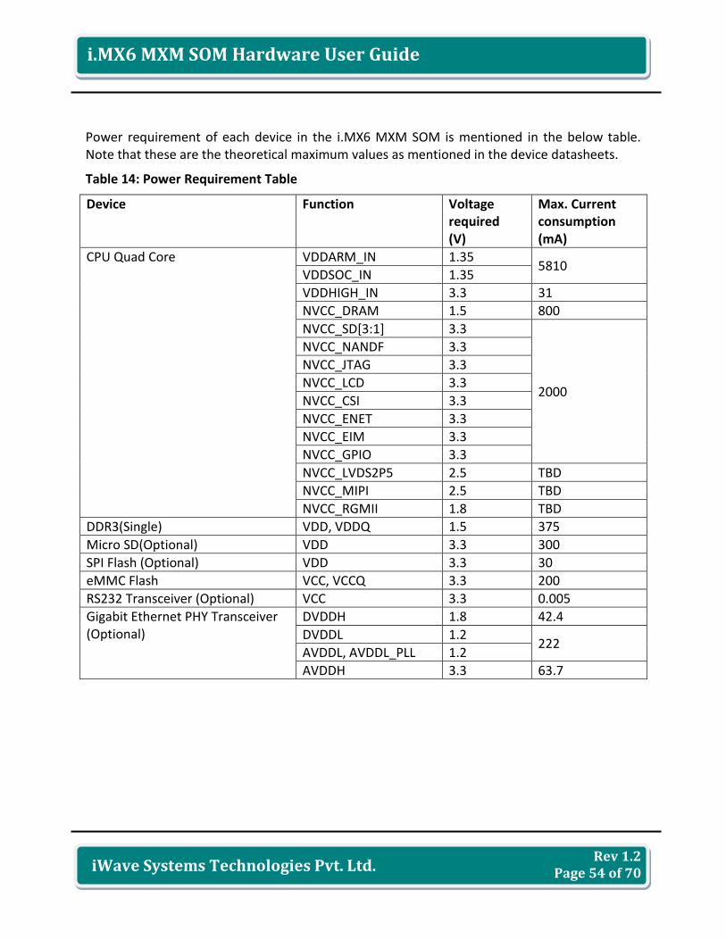
Power requirement of each device in the i.MX6 MXM SOM is mentioned in the below table. Note that these are the theoretical maximum values as mentioned in the device datasheets.
Table 14: Power Requirement Table
Device Function Voltage required (V)
Max. Current consumption (mA)
CPU Quad Core VDDARM_IN 1.35 5810
VDDSOC_IN 1.35
VDDHIGH_IN 3.3 31
NVCC_DRAM 1.5 800
NVCC_SD[3:1] 3.3
2000
NVCC_NANDF 3.3
NVCC_JTAG 3.3
NVCC_LCD 3.3
NVCC_CSI 3.3
NVCC_ENET 3.3
NVCC_EIM 3.3
NVCC_GPIO 3.3
NVCC_LVDS2P5 2.5 TBD
NVCC_MIPI 2.5 TBD
NVCC_RGMII 1.8 TBD
DDR3(Single) VDD, VDDQ 1.5 375
Micro SD(Optional) VDD 3.3 300
SPI Flash (Optional) VDD 3.3 30
eMMC Flash VCC, VCCQ 3.3 200
RS232 Transceiver (Optional) VCC 3.3 0.005
Gigabit Ethernet PHY Transceiver (Optional)
DVDDH 1.8 42.4
DVDDL 1.2 222
AVDDL, AVDDL_PLL 1.2
AVDDH 3.3 63.7
Rev 1.2 Page 55 of 70
i.MX6 MXM SOM Hardware User Guide
iWave Systems Technologies Pvt. Ltd.
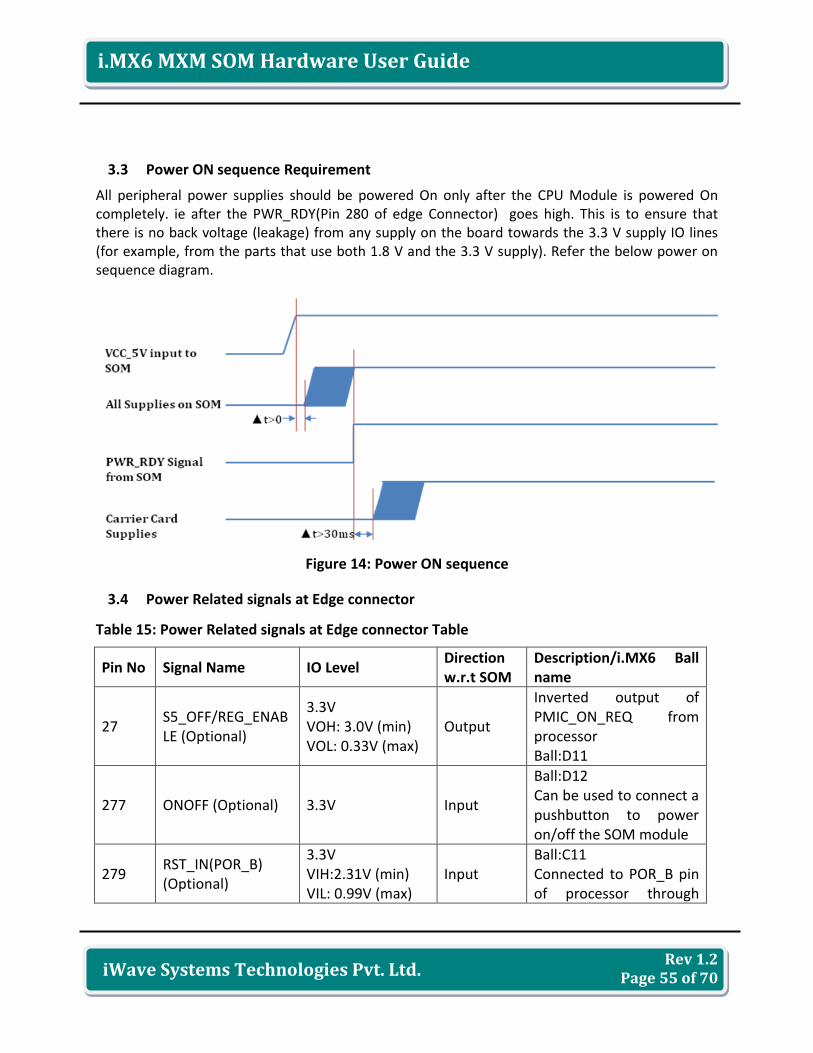
3.3 Power ON sequence Requirement
All peripheral power supplies should be powered On only after the CPU Module is powered On completely. ie after the PWR_RDY(Pin 280 of edge Connector) goes high. This is to ensure that there is no back voltage (leakage) from any supply on the board towards the 3.3 V supply IO lines (for example, from the parts that use both 1.8 V and the 3.3 V supply). Refer the below power on sequence diagram.
Figure 14: Power ON sequence
3.4 Power Related signals at Edge connector
Table 15: Power Related signals at Edge connector Table
Pin No Signal Name IO Level Direction w.r.t SOM
Description/i.MX6 Ball name
27 S5_OFF/REG_ENABLE (Optional)
3.3V VOH: 3.0V (min) VOL: 0.33V (max)
Output
Inverted output of PMIC_ON_REQ from processor Ball:D11
277 ONOFF (Optional) 3.3V Input
Ball:D12 Can be used to connect a pushbutton to power on/off the SOM module
279 RST_IN(POR_B) (Optional)
3.3V VIH:2.31V (min) VIL: 0.99V (max)
Input Ball:C11 Connected to POR_B pin of processor through
Rev 1.2 Page 56 of 70
i.MX6 MXM SOM Hardware User Guide
iWave Systems Technologies Pvt. Ltd.
reset IC. Can be used to connect a reset switch on the carrier card to reset the SOM module
280 PWR_RDY 3.3V VOH: 3.0V (min) VOL: 0.4V (max)
Output
Power Ready signal of SOM. Pull to last supply on SOM(3.3V) Used for power on sequencing of carrier board
281 SLEEP (Optional) 3.3V VOH: 3.0V (min) VOL: 0.33V (max)
Output
Ball: F11 Optional. Inverted output of PMIC_VSTBY_REQ signal from processor
S5_OFF (Pin 27) is an optional power management signal which is an inverted output of PMIC_ON_REQ signal from processor. When PMIC_ON_REQ goes high (S5_OFFLow) the supplies on iMX6 MXM SOM will be turned off except the supply to i.MX6 internal PMIC. When PMIC_ON_REQ goes low (S5_OFFHigh) the supplies on iMX6 MXM SOM will be turned on & will work normally. Not that the current software version does not support this feature so i.MX6 MXM SOM will operate without depending on S5_OFF signal. SLEEP (Pin 281) is an optional power management signal which is an inverted output of PMIC_STBY_REQ signal from processor. This signal is not used in iMX6 MXM SOM. ONOFF (Pin 277) is connected to ONOFF pin of i.MX6 processor. In normal mode may be connected to ON/OFF button (De-bouncing provided at this input).Internally this pad is pulled up. Short connection to GND in OFF mode causes internal power management state machine to change state to ON. In ON mode short connection to GND generates interrupt (intended to SW controllable power down). Long above ~5s connection to GND causes “forced” OFF. Please refer i.MX6 User Manual “System Reset Controller (SRC)” chapter for more details on these power management signals. RST_IN (POR_B) (Pin 279) is a reset input signal to the processor. This signal is connected to the manual reset pin of the reset IC on the MXM SOM. This signal can be used to connect a Reset Switch on the carrier board. A low on this signal generates a reset delay of 20ms to the processor & the processor will reboot. PWR_RDY (Pin 280) is output from SOM. A 1K pull up to 3.3V is provided on SOM. This signal can be used to enable the supplies on carrier card.
Rev 1.2 Page 57 of 70
i.MX6 MXM SOM Hardware User Guide
iWave Systems Technologies Pvt. Ltd.
3.5 LED Description
Once the module is turned ON, the RED LED on the module will glow indicating that the SOM supplies are proper. If LED is OFF indicates that on SOM supplies are not proper.
3.6 i.MX6 MXM SOM Interface Requirement
Below are the details on the connection requirement for some of high speed interface available at the Edge & Expansion connector. Please refer the i.MX6 Datasheet for electrical specifications of the interface.
3.6.1 PCIE Interface Requirement
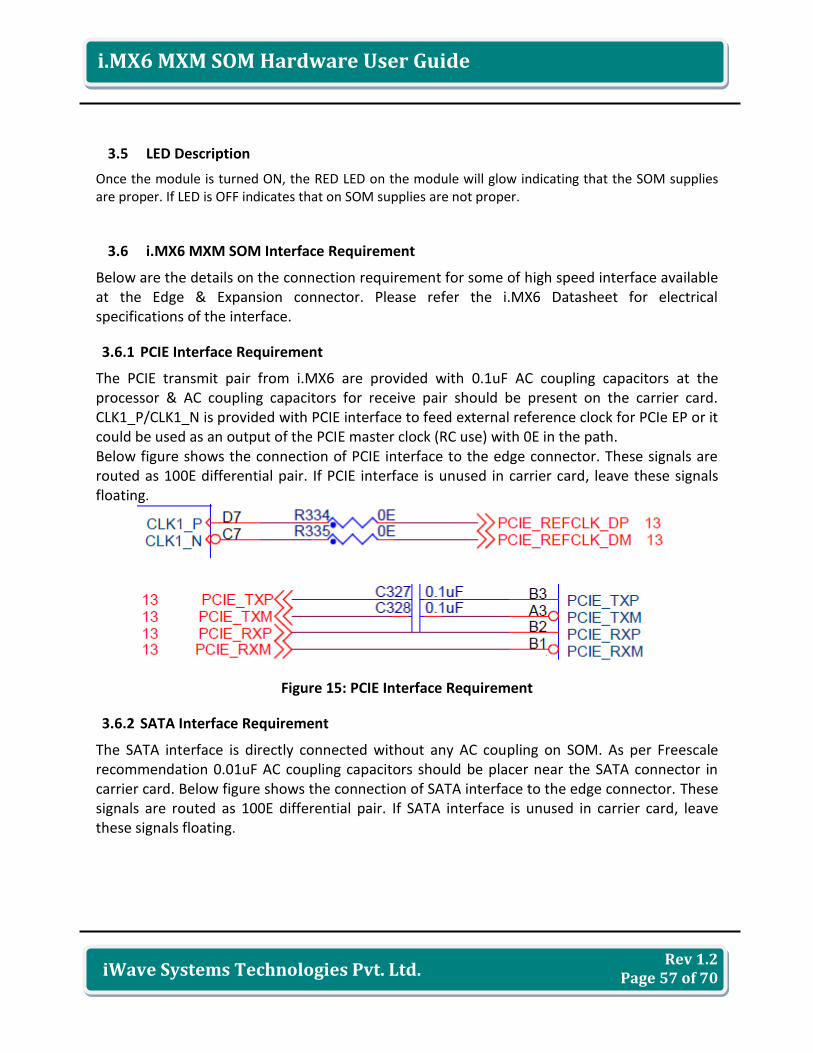
The PCIE transmit pair from i.MX6 are provided with 0.1uF AC coupling capacitors at the processor & AC coupling capacitors for receive pair should be present on the carrier card. CLK1_P/CLK1_N is provided with PCIE interface to feed external reference clock for PCIe EP or it could be used as an output of the PCIE master clock (RC use) with 0E in the path. Below figure shows the connection of PCIE interface to the edge connector. These signals are routed as 100E differential pair. If PCIE interface is unused in carrier card, leave these signals floating.
Figure 15: PCIE Interface Requirement
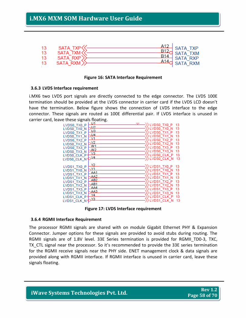
3.6.2 SATA Interface Requirement
The SATA interface is directly connected without any AC coupling on SOM. As per Freescale recommendation 0.01uF AC coupling capacitors should be placer near the SATA connector in carrier card. Below figure shows the connection of SATA interface to the edge connector. These signals are routed as 100E differential pair. If SATA interface is unused in carrier card, leave these signals floating.
Rev 1.2 Page 58 of 70
i.MX6 MXM SOM Hardware User Guide
iWave Systems Technologies Pvt. Ltd.
Figure 16: SATA Interface Requirement
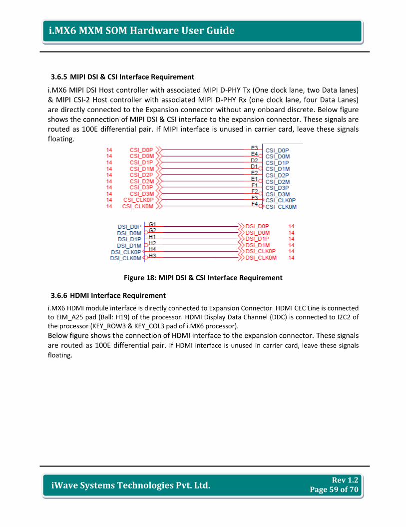
3.6.3 LVDS Interface requirement
i.MX6 two LVDS port signals are directly connected to the edge connector. The LVDS 100E termination should be provided at the LVDS connector in carrier card if the LVDS LCD doesn’t have the termination. Below figure shows the connection of LVDS interface to the edge connector. These signals are routed as 100E differential pair. If LVDS interface is unused in carrier card, leave these signals floating.
Figure 17: LVDS Interface requirement
3.6.4 RGMII Interface Requirement
The processor RGMII signals are shared with on module Gigabit Ethernet PHY & Expansion Connector. Jumper options for these signals are provided to avoid stubs during routing. The RGMII signals are of 1.8V level. 33E Series termination is provided for RGMII_TD0-3, TXC, TX_CTL signal near the processor. So it’s recommended to provide the 33E series termination for the RGMII receive signals near the PHY side. ENET management clock & data signals are provided along with RGMII interface. If RGMII interface is unused in carrier card, leave these signals floating.
Rev 1.2 Page 59 of 70
i.MX6 MXM SOM Hardware User Guide
iWave Systems Technologies Pvt. Ltd.
3.6.5 MIPI DSI & CSI Interface Requirement
i.MX6 MIPI DSI Host controller with associated MIPI D-PHY Tx (One clock lane, two Data lanes) & MIPI CSI-2 Host controller with associated MIPI D-PHY Rx (one clock lane, four Data Lanes) are directly connected to the Expansion connector without any onboard discrete. Below figure shows the connection of MIPI DSI & CSI interface to the expansion connector. These signals are routed as 100E differential pair. If MIPI interface is unused in carrier card, leave these signals floating.
Figure 18: MIPI DSI & CSI Interface Requirement
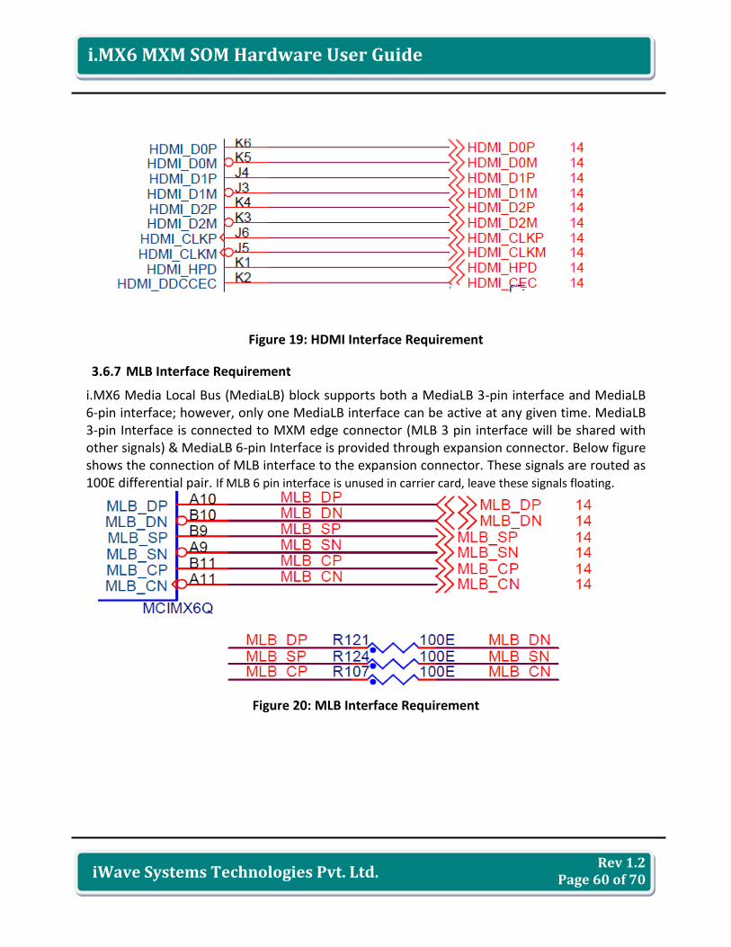
3.6.6 HDMI Interface Requirement
i.MX6 HDMI module interface is directly connected to Expansion Connector. HDMI CEC Line is connected to EIM_A25 pad (Ball: H19) of the processor. HDMI Display Data Channel (DDC) is connected to I2C2 of the processor (KEY_ROW3 & KEY_COL3 pad of i.MX6 processor).
Below figure shows the connection of HDMI interface to the expansion connector. These signals are routed as 100E differential pair. If HDMI interface is unused in carrier card, leave these signals
floating.
Rev 1.2 Page 60 of 70
i.MX6 MXM SOM Hardware User Guide
iWave Systems Technologies Pvt. Ltd.
Figure 19: HDMI Interface Requirement
3.6.7 MLB Interface Requirement
i.MX6 Media Local Bus (MediaLB) block supports both a MediaLB 3-pin interface and MediaLB 6-pin interface; however, only one MediaLB interface can be active at any given time. MediaLB 3-pin Interface is connected to MXM edge connector (MLB 3 pin interface will be shared with other signals) & MediaLB 6-pin Interface is provided through expansion connector. Below figure shows the connection of MLB interface to the expansion connector. These signals are routed as 100E differential pair. If MLB 6 pin interface is unused in carrier card, leave these signals floating.
Figure 20: MLB Interface Requirement
Rev 1.2 Page 61 of 70
i.MX6 MXM SOM Hardware User Guide
iWave Systems Technologies Pvt. Ltd.
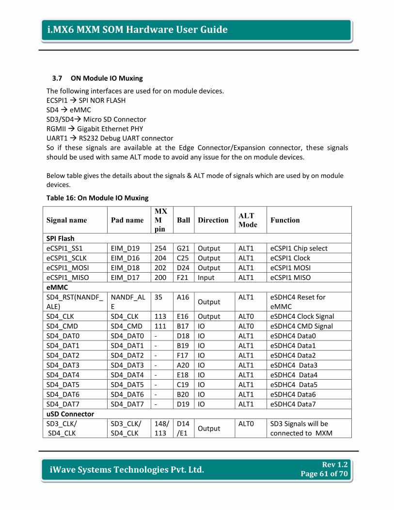
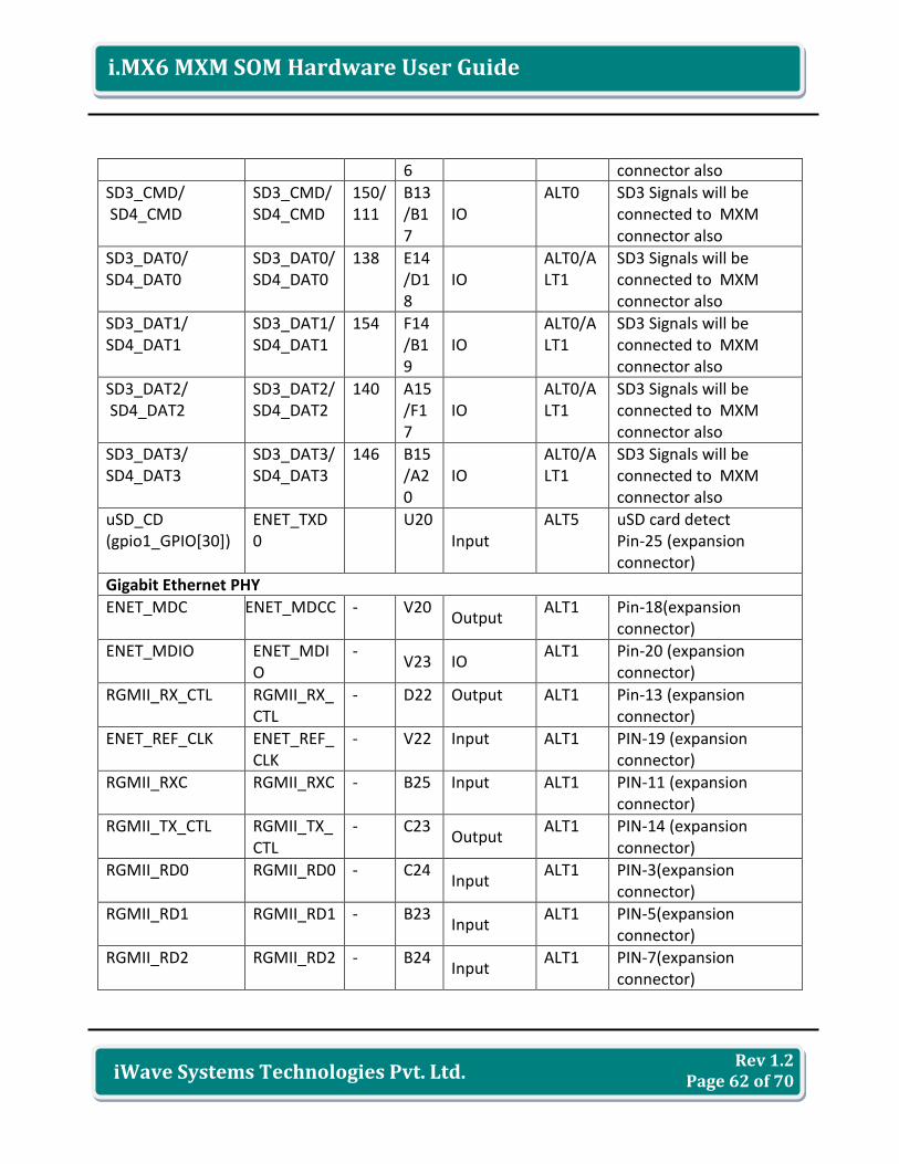
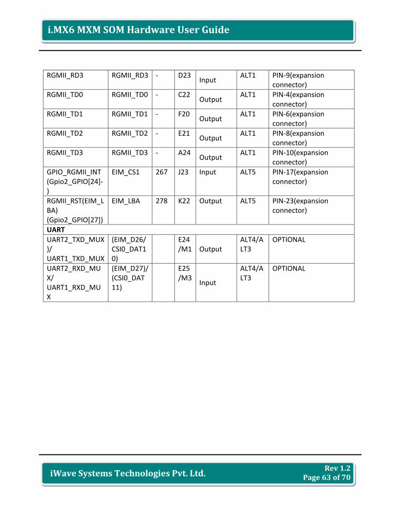
3.7 ON Module IO Muxing
The following interfaces are used for on module devices. ECSPI1 SPI NOR FLASH SD4 eMMC SD3/SD4 Micro SD Connector RGMII Gigabit Ethernet PHY UART1 RS232 Debug UART connector So if these signals are available at the Edge Connector/Expansion connector, these signals should be used with same ALT mode to avoid any issue for the on module devices. Below table gives the details about the signals & ALT mode of signals which are used by on module devices.
Table 16: On Module IO Muxing
Signal name Pad name
MX
M
pin
Ball Direction ALT
Mode Function
SPI Flash
eCSPI1_SS1 EIM_D19 254 G21 Output ALT1 eCSPI1 Chip select
eCSPI1_SCLK EIM_D16 204 C25 Output ALT1 eCSPI1 Clock
eCSPI1_MOSI EIM_D18 202 D24 Output ALT1 eCSPI1 MOSI
eCSPI1_MISO EIM_D17 200 F21 Input ALT1 eCSPI1 MISO
eMMC
SD4_RST(NANDF_ALE)
NANDF_ALE
35 A16 Output
ALT1 eSDHC4 Reset for eMMC
SD4_CLK SD4_CLK 113 E16 Output ALT0 eSDHC4 Clock Signal
SD4_CMD SD4_CMD 111 B17 IO ALT0 eSDHC4 CMD Signal
SD4_DAT0 SD4_DAT0 - D18 IO ALT1 eSDHC4 Data0
SD4_DAT1 SD4_DAT1 - B19 IO ALT1 eSDHC4 Data1
SD4_DAT2 SD4_DAT2 - F17 IO ALT1 eSDHC4 Data2
SD4_DAT3 SD4_DAT3 - A20 IO ALT1 eSDHC4 Data3
SD4_DAT4 SD4_DAT4 - E18 IO ALT1 eSDHC4 Data4
SD4_DAT5 SD4_DAT5 - C19 IO ALT1 eSDHC4 Data5
SD4_DAT6 SD4_DAT6 - B20 IO ALT1 eSDHC4 Data6
SD4_DAT7 SD4_DAT7 - D19 IO ALT1 eSDHC4 Data7
uSD Connector
SD3_CLK/ SD4_CLK
SD3_CLK/ SD4_CLK
148/ 113
D14/E1
Output ALT0 SD3 Signals will be
connected to MXM
Rev 1.2 Page 62 of 70
i.MX6 MXM SOM Hardware User Guide
iWave Systems Technologies Pvt. Ltd.
6 connector also
SD3_CMD/ SD4_CMD
SD3_CMD/ SD4_CMD
150/ 111
B13/B17
IO ALT0 SD3 Signals will be
connected to MXM connector also
SD3_DAT0/ SD4_DAT0
SD3_DAT0/ SD4_DAT0
138 E14/D18
IO ALT0/ALT1
SD3 Signals will be connected to MXM connector also
SD3_DAT1/ SD4_DAT1
SD3_DAT1/ SD4_DAT1
154 F14/B19
IO ALT0/ALT1
SD3 Signals will be connected to MXM connector also
SD3_DAT2/ SD4_DAT2
SD3_DAT2/ SD4_DAT2
140 A15/F17
IO ALT0/ALT1
SD3 Signals will be connected to MXM connector also
SD3_DAT3/ SD4_DAT3
SD3_DAT3/ SD4_DAT3
146 B15/A20
IO ALT0/ALT1
SD3 Signals will be connected to MXM connector also
uSD_CD (gpio1_GPIO[30])
ENET_TXD0
U20 Input
ALT5 uSD card detect Pin-25 (expansion connector)
Gigabit Ethernet PHY
ENET_MDC ENET_MDCC - V20 Output
ALT1 Pin-18(expansion connector)
ENET_MDIO ENET_MDIO
- V23 IO
ALT1 Pin-20 (expansion connector)
RGMII_RX_CTL RGMII_RX_CTL
- D22 Output ALT1 Pin-13 (expansion connector)
ENET_REF_CLK ENET_REF_CLK
- V22 Input ALT1 PIN-19 (expansion connector)
RGMII_RXC RGMII_RXC - B25 Input ALT1 PIN-11 (expansion connector)
RGMII_TX_CTL RGMII_TX_CTL
- C23 Output
ALT1 PIN-14 (expansion connector)
RGMII_RD0 RGMII_RD0 - C24 Input
ALT1 PIN-3(expansion connector)
RGMII_RD1 RGMII_RD1 - B23 Input
ALT1 PIN-5(expansion connector)
RGMII_RD2 RGMII_RD2 - B24 Input
ALT1 PIN-7(expansion connector)
Rev 1.2 Page 63 of 70
i.MX6 MXM SOM Hardware User Guide
iWave Systems Technologies Pvt. Ltd.
RGMII_RD3 RGMII_RD3 - D23 Input
ALT1 PIN-9(expansion connector)
RGMII_TD0 RGMII_TD0 - C22 Output
ALT1 PIN-4(expansion connector)
RGMII_TD1 RGMII_TD1 - F20 Output
ALT1 PIN-6(expansion connector)
RGMII_TD2 RGMII_TD2 - E21 Output
ALT1 PIN-8(expansion connector)
RGMII_TD3 RGMII_TD3 - A24 Output
ALT1 PIN-10(expansion connector)
GPIO_RGMII_INT (Gpio2_GPIO[24]-)
EIM_CS1 267 J23 Input ALT5 PIN-17(expansion connector)
RGMII_RST(EIM_LBA) (Gpio2_GPIO[27])
EIM_LBA 278 K22 Output ALT5 PIN-23(expansion connector)
UART
UART2_TXD_MUX)/ UART1_TXD_MUX
(EIM_D26/ CSI0_DAT10)
E24/M1 Output
ALT4/ALT3
OPTIONAL
UART2_RXD_MUX/ UART1_RXD_MUX
(EIM_D27)/ (CSI0_DAT11)
E25/M3
Input
ALT4/ALT3
OPTIONAL
Rev 1.2 Page 64 of 70
i.MX6 MXM SOM Hardware User Guide
iWave Systems Technologies Pvt. Ltd.
4. MECHANICAL INFORMATION
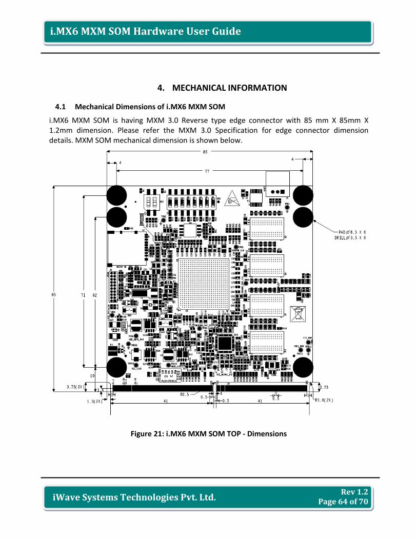
4.1 Mechanical Dimensions of i.MX6 MXM SOM
i.MX6 MXM SOM is having MXM 3.0 Reverse type edge connector with 85 mm X 85mm X 1.2mm dimension. Please refer the MXM 3.0 Specification for edge connector dimension details. MXM SOM mechanical dimension is shown below.
Figure 21: i.MX6 MXM SOM TOP - Dimensions
Rev 1.2 Page 65 of 70
i.MX6 MXM SOM Hardware User Guide
iWave Systems Technologies Pvt. Ltd.
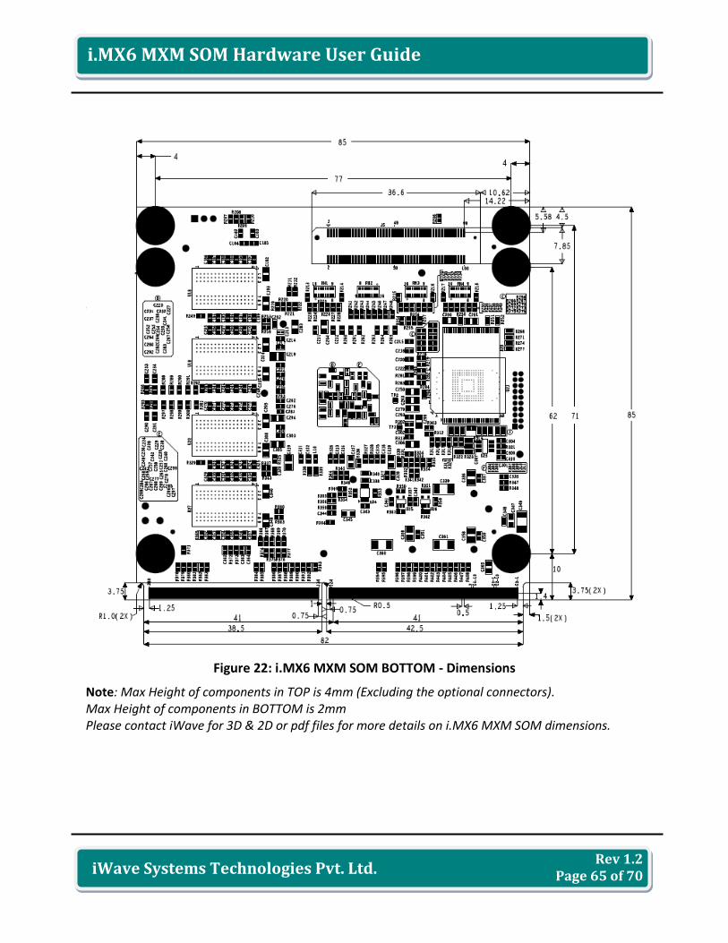
Figure 22: i.MX6 MXM SOM BOTTOM - Dimensions
Note: Max Height of components in TOP is 4mm (Excluding the optional connectors). Max Height of components in BOTTOM is 2mm Please contact iWave for 3D & 2D or pdf files for more details on i.MX6 MXM SOM dimensions.
Rev 1.2 Page 66 of 70
i.MX6 MXM SOM Hardware User Guide
iWave Systems Technologies Pvt. Ltd.
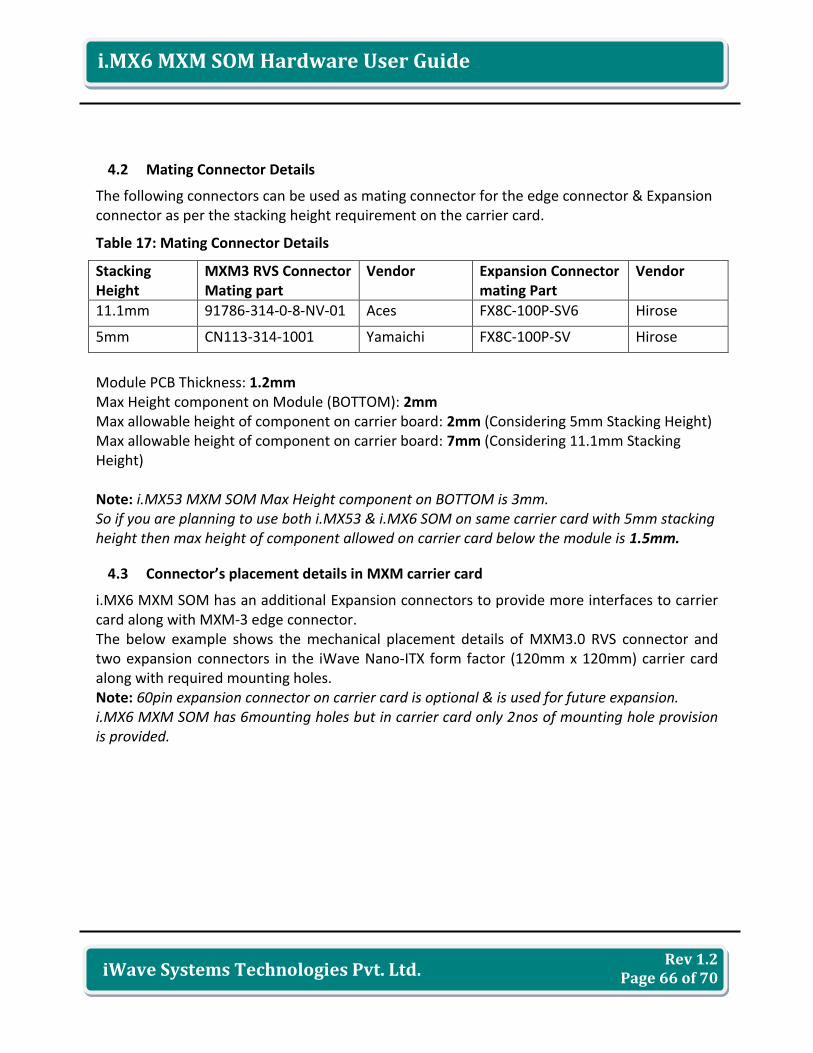
4.2 Mating Connector Details
The following connectors can be used as mating connector for the edge connector & Expansion connector as per the stacking height requirement on the carrier card.
Table 17: Mating Connector Details
Stacking Height
MXM3 RVS Connector Mating part
Vendor Expansion Connector mating Part
Vendor
11.1mm 91786-314-0-8-NV-01 Aces FX8C-100P-SV6 Hirose
5mm CN113-314-1001 Yamaichi FX8C-100P-SV Hirose
Module PCB Thickness: 1.2mm Max Height component on Module (BOTTOM): 2mm Max allowable height of component on carrier board: 2mm (Considering 5mm Stacking Height) Max allowable height of component on carrier board: 7mm (Considering 11.1mm Stacking Height) Note: i.MX53 MXM SOM Max Height component on BOTTOM is 3mm. So if you are planning to use both i.MX53 & i.MX6 SOM on same carrier card with 5mm stacking height then max height of component allowed on carrier card below the module is 1.5mm.
4.3 Connector’s placement details in MXM carrier card
i.MX6 MXM SOM has an additional Expansion connectors to provide more interfaces to carrier card along with MXM-3 edge connector. The below example shows the mechanical placement details of MXM3.0 RVS connector and two expansion connectors in the iWave Nano-ITX form factor (120mm x 120mm) carrier card along with required mounting holes. Note: 60pin expansion connector on carrier card is optional & is used for future expansion. i.MX6 MXM SOM has 6mounting holes but in carrier card only 2nos of mounting hole provision is provided.
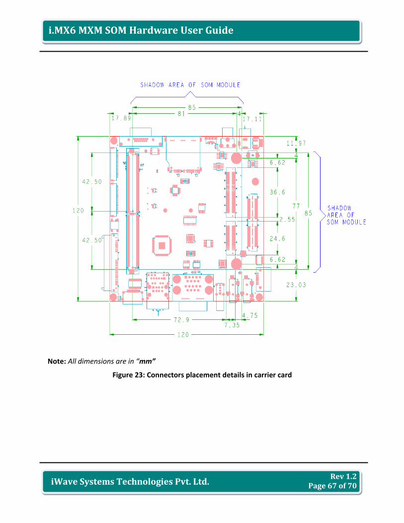
Rev 1.2 Page 67 of 70
i.MX6 MXM SOM Hardware User Guide
iWave Systems Technologies Pvt. Ltd.
Note: All dimensions are in “mm”
Figure 23: Connectors placement details in carrier card
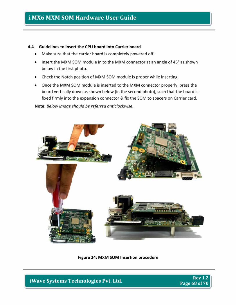
Rev 1.2 Page 68 of 70
i.MX6 MXM SOM Hardware User Guide
iWave Systems Technologies Pvt. Ltd.
4.4 Guidelines to insert the CPU board into Carrier board
Make sure that the carrier board is completely powered off.
Insert the MXM SOM module in to the MXM connector at an angle of 45° as shown
below in the first photo.
Check the Notch position of MXM SOM module is proper while inserting.
Once the MXM SOM module is inserted to the MXM connector properly, press the
board vertically down as shown below (in the second photo), such that the board is
fixed firmly into the expansion connector & fix the SOM to spacers on Carrier card.
Note: Below image should be referred anticlockwise.
Figure 24: MXM SOM Insertion procedure
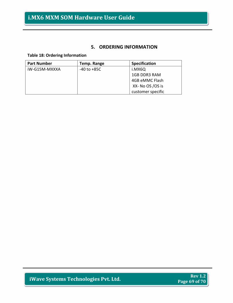
Rev 1.2 Page 69 of 70
i.MX6 MXM SOM Hardware User Guide
iWave Systems Technologies Pvt. Ltd.
5. ORDERING INFORMATION
Table 18: Ordering Information
Part Number Temp. Range Specification
iW-G15M-MXXXA -40 to +85C i.MX6Q 1GB DDR3 RAM 4GB eMMC Flash XX- No OS /OS is customer specific
Rev 1.2 Page 70 of 70
i.MX6 MXM SOM Hardware User Guide
iWave Systems Technologies Pvt. Ltd.
6. TECHNICAL SUPPORT
iWave Systems Technologies Pvt. Ltd. # 7/B, 29th Main, BTM Layout 2nd Stage, Bangalore – 560 076 Phone : +91-80-26683700, 26786245 Fax : +91-80-26685200 Email : [email protected] Website: www.iwavesystems.com


![Cartaz_Polichinello[08-04-15] mxm d](https://static.fdocuments.in/doc/165x107/55cf9193550346f57b8ea771/cartazpolichinello08-04-15-mxm-d.jpg)