Improvement Potential and Equalization Circuit Solutions for Multi-drop DRAM Memory Buses
179
Linköping Studies in Science and Technology Dissertation No. 1177 Improvement Potential and Equalization Circuit Solutions for Multi-drop DRAM Memory Buses Henrik Fredriksson Electronic Devices Department of Electrical Engineering Linköpings universitet, SE-581 83 Linköping, Sweden Linköping 2008 ISBN 978-91-7393-910-2 ISSN 0345-7524
Transcript of Improvement Potential and Equalization Circuit Solutions for Multi-drop DRAM Memory Buses
Linköping Studies in Science and TechnologyDissertation No. 1177
Improvement Potential andEqualization Circuit Solutions forMulti-drop DRAM Memory Buses
Henrik Fredriksson
Electronic DevicesDepartment of Electrical Engineering
Linköpings universitet, SE-581 83 Linköping, Sweden
Linköping 2008
ISBN 978-91-7393-910-2ISSN 0345-7524

ii
Improvement Potential and Equalization Circuit Solutions for Multi-drop
DRAM Memory Buses
Henrik Fredriksson
ISBN 978-91-7393-910-2
Copyright c©Henrik Fredriksson, 2008
Linköping Studies in Science and TechnologyDissertation No. 1177ISSN 0345-7524
Electronic DevicesDepartment of Electrical EngineeringLinköping UniversitySE-581 83 LinköpingSWEDEN
Cover Image
The eye diagram monster.Eye diagram appearing at the oscilloscope 2007-09-09 while evaluating testchip 2. Measured over the receiver chip off-chip termination resistor whiletransmitting PRBS data at 2.0 Gb/s in DIMM configuration B2 (see chapter 10)
Thesis subtitle:How to defeat the eye diagram monster
Printed by LiU-Tryck, Linköping UniversityLinköping Sweden, May 2008

Abstract
Digital computers have changed human society in a profound way over the last50 years. Key properties that contribute to the success of the computer are flex-ible programmability and fast access to large amounts of data and instructions.Effective access to algorithms and data is a fundamental property that limits thecapabilities of computer systems. For PC computers, the main memory consistsof dynamic random access memory (DRAM). Communication between memoryand processor has traditionally been performed over a multi-drop bus.
Signal frequencies on these buses have gradually increased in order to keepup with the progress in integrated circuit data processing capabilities. Increasedsignal frequencies have exposed the inherent signal degradation effects of a multi-drop bus structure. As of today, the main approach to tackle these effects hasbeen to reduce the number of endpoints of the bus structure. Though improve-ments in DRAM memory technology have increased the available memory sizeat each endpoint, the increase has not been able to fully fulfill the demand forlarger system memory capacity. Different bus structural changes have been usedto overcome this problem. All are different compromises between access latency,data transmission capacity, memory capacity, and implementation costs.
In this thesis we focus on using the signal processing capabilities of a modernintegrated circuit technology as an alternative to bus structural changes. This hasthe potential to give low latency, high memory capacity, and relatively high datatransmission capacity at an additional cost limited to integrated circuit blocks.
We first use information theory to estimate the unexplored potential of exist-ing multi-drop bus structures. Hereby showing that reduction of the number ofendpoints for multi-drop buses, is by no means based on the fundamental limitof the data transmission capacity of the bus structure. Two test-chips have beendesigned and fabricated to experimentally demonstrate the feasibility of severalGb/s data-rates over multi-drop buses, with limited cost overhead and no latencypenalty. The test-chips implement decision feedback equalization, adopted forhigh speed multi-drop use. The equalizers feature digital filter implementationswhich, in combination with high speed DACs, enable the use of long digital filtersfor high speed decision feedback equalization. Blind adaptation has also been im-
iii

iv
plemented to demonstrate extraction of channel characteristics during data trans-mission. The use of single sided equalization has been proposed in order to limitthe need for equalization implementation to the host side of a DRAM memorybus. Furthermore, we propose to utilize the reciprocal properties of the communi-cation channel to ensure that single sided equalization can be performed withoutany channel characterization hardware on the memory chips.
Finally, issues related to evaluation of high-speed channels are addressed andthe on-chip structures used for channel evaluation in this project are presented.

Populärvetenskaplig
Sammanfattning
Den snabba utvecklingen av integrerade kretsar erbjuder en enorm beräkningska-pacitet i dagens mikroprocessorer. Dessa processorer klarar av att hantera störreprogram och enormt mycket mer data än bara för några år sedan. Tillgång tillsnabba och stora minnen att lagra dessa data i är mycket viktigt för att kunnautnyttja processorerna effektivt. Av tekniska och affärsmässiga skäl konstruerasminnen och processorer i separata integrerade kretsar. Det är idag en utmaning attöverföra data mellan dessa kretsar tillräckligt snabbt och effektivt.
Datorns arbetsminne består idag och sedan länge av DIMM-moduler medDRAM minnen. Det finns i allmänhet ett antal elektriskt hopkopplade kontakteri datorn där konsumenterna själva kan stoppa in nya moduler för att uppgraderasina datorer med mer minne. Att ha flera moduler elektriskt kopplade till varandrapå detta sätt ställer till problem när vill skicka data allt snabbare. Data skickasidag så snabbt att signalerna, som representerar data, studsar fram och tillbaka iledningarna innan de kommer fram vilket gör det svårt att reda ut vad signalernabetyder när dessa kommer fram. För att minska dessa effekter har man minskatpå antalet kontakter där man kan sätta in DIMM-moduler. Även om mängdenminne per DIMM-modul har ökat enormt har kraven på den totala mängden minneökat ännu snabbare. Det finns därför ett problem med att den maximala mängdenminne som kan kopplas in är för liten.
För att råda bot på detta problem har datortillverkarna delat upp minnesko-rtplatserna i flera parallella elektriskt oberoende system. Detta gör dock prisetför datorerna högre vilket inte alltid tolereras på en pressad marknad. Det finnsäven system som erbjuder större maximala minnesmängder på bekostnad av län-gre väntetider innan data levereras. Dock är dessa svåra att göra billiga då de ävenkräver fler IC-kretsar.
Problem med att signaler studsar och därmed är svår att tyda för mottagarenfinns i andra sammanhang. Inom till exempel mobiltelefoni skapar radiovågorsom studsar mot berg och hus samma typ av effekter. Mobiltelefonsystemen an-vänder smarta algoritmer för att kompensera för detta. I denna avhandling använ-
v

vi
der vi samma typer av algoritmer för att kompensera för studsande signaler vidkommunikationen mellan mikroprocessor och arbetsminne i en dator.
Överföringshastigheterna är dock enormt mycket högre i en dator än för mo-biltelefoner. Kompenseringsalgoritmerna måste därför hållas enkla och de be-höver göras som specialbyggda kretsblock på IC-kretsarna.
I denna avhandling börjar vi med att visa att den teoretiskt maximala data-hastigheten är i storleksordningen hundra gånger högre än vad som används kom-mersiellt. Det finns därför en potential att öka datahastigheterna utan att ändra påarkitekturen. Vi presenterar mätningar på egenkonstruerade kretsar som visar attdet går att minska detta glapp mellan teoretiskt maximala och praktiskt andvänd-bara datahastigheter. Dessa kretsar klarar av att ta emot data i storleksordningentio gånger snabbare än vad som används kommersiellt. För att få en så billig lös-ning som möjligt visar vi även på möjligheten att lägga alla kompenseringskretsari ena ändan av signalöverföringskanalen. Genom att utnyttja symmetriegenskaperhos signalöverföringskanalen och så kallade blinda anpassningsalgoritmer kan viföreslå en lösning som inte kräver längre väntetider, fler IC-kretsar eller störremodifieringar av minneskretsarna. Detta är en lösning som klarar höga hastighetermed ett stort antal kontakter och därmed möjligheten att koppla in en stor mängdminne till en billig kostnad.

Preface
This thesis presents my research during the period from September 2003 to April2008 at the Electronic Devices group, Department of Electrical Engineering, Lin-köping University, Sweden.
The starting point for the research activities was cooperation between threesemiconductor companies and Professor Christer Svensson, the supervisor of thisproject, to tackle the problem of communication between DRAM memory mod-ules and the processor in a PC. Samsung Electronics and Infineon Technologies1
have been involved from the memory side of the communication channel and IntelInc. from the host, or processor, side. These companies have given valuable inputand financial support to this project
Most of the results presented in this thesis have been previously published.However, some additional results are included and published topics are covered inmore detail in this thesis.
This thesis is based on the following publications:
Henrik Fredriksson and Christer Svensson, “Mixed-Signal Decision Feed-back Equalizer for Multi-Drop, Gb/s, Memory Buses — a Feasibility Study”,in IEEE International SOC Conference, 2004 (SOCC). Proceedings, pp. 147-148, Santa Clara, Carlifonia, USA, September 2004.
The paper discuss the channel characteristics of a multi-drop bus as in chap-ter 3 and the DFE implementation structure in chapter 8.
Henrik Fredriksson and Christer Svensson, “Blind Adaptive Mixed-SignalDFE for Gb/s, Multi-Drop, Buses”, in IEEE International Symposium on
VLSI Design, Automation and Test 2006 (VLSI-DAT). Proceedings, pp. 223-226, Hsinchu, Taiwan, April. 2006.
The paper discuss the implementation structure described in chapter 8, theevaluation circuits described in chapter 9, and measurement result from testchip 1 as described in chapter 10.
1The DRAM memory division of Infineon is now the company Qimonda.
vii

viii
Henrik Fredriksson, Christer Svensson,and Atila Alvandpour “A 3.4 Gb/bLow Latency 1 Bit Input Digital FIR-Filter in 0.13 µm CMOS” in Pro-
ceedings of the 14th International Conference MIXED DESIGN OF INTE-
GRATED CIRCUITS AND SYSTEMS (MIXDES), pp. 181-184, Ciechocinek,Poland, June 2007.
The paper presents the improved digital filter implementation used in testchip 2 as described in chapter 8.
Henrik Fredriksson and Christer Svensson, “3-Gb/s, Single-Ended Adap-tive Equalization of Bidirectional Data over a Multi-drop Bus” Proceedings
of 2007 International Symposium on System-on-Chip, pp. 125-128, Tam-pere, Finland, November 2007.
The paper presents the extension of the DFE to a linear transmit equalizerand the use of reciprocity to enable single sided equalization as describedin chapter 11.
Henrik Fredriksson and Christer Svensson, “Improvement potential andequalization example for multi-drop DRAM memory buses”
This manuscript has been submitted to IEEE Transactions on Advanced
Packaging.
The article describe the capacity of a multi-drop channel as described inchapter 3, implementation structure and measurement results for test chip 2as described in chapter 8 and chapter 10.
Henrik Fredriksson and Christer Svensson, “2.6 Gb/s over a four-drop bususing an adaptive 12-Tap DFE”
This manuscript has been submitted to the 34th European Solid-State Cir-
cuit Conference (ESSCIRC) 2008.
The paper presents implementation structures, adaptation algorithm, evalu-ation circuits and measurement results for test chip 2 as described in chap-ters 8, 9, and 10.
Other related publications:
Henrik Fredriksson and Christer Svensson, “Gb/s equalizer for multi-dropmemory buses” in Swedish System-on-Chip Conference (SSoCC) Proceed-
ings, Båstad, Sweden April. 2004.
Henrik Fredriksson and Christer Svensson, “0.18 µm CMOS chip for eval-uation of Gb/s equalizer for multi-drop memory buses” in Swedish System-
on-Chip Conference (SSoCC) Proceedings, Tammsvik, Sweden April. 2005.

ix
Henrik Fredriksson and Christer Svensson, “Blind Adaptive Mixed-SignalDFE for a Four Drop Memory Bus” in Swedish System-on-Chip Conference
(SSoCC) Proceedings, Kolmården, Sweden April. 2006.
Henrik Fredriksson and Christer Svensson, “Single-ended adaptive equal-ization of bidirectional data communication utilizing reciprocity” in Swedish
System-on-Chip Conference (SSoCC) Proceedings, Fiskebäckskil , SwedenMay. 2007.
I have also been involved in research work, which has generated the followingpaper, falling outside the scope of this thesis:
Peter Caputa, Henrik Fredriksson, Martin Hansson, StefanAndersson, Atila Alvandpour, and Christer Svensson, “An Extended Tran-sition Energy Cost Model for Buses in Deep Submicron Technologies”, inProceedings of the Power and Timing Modeling, Optimization and Simula-
tion Conference, pp. 849-858, Santorini, Greece, September 2004.

x

Contributions
The main contributions of this dissertation are as follows:
• Estimation of unexplored potential of multi-drop bus communication.
• The idea of using the reciprocal properties of a multi-drop bus to enableimplementation of communication improvement circuitry at one end of thebus.
• A FIR filter implementation strategy that enables the use of long digitalfilters for high speed DFE implementations.
• Implementation of blind adaptation for a DFE with internal offset compen-sation and small circuit overhead.
• Implementation of high speed bit error rate evaluation and on chip eye dia-gram extraction circuitry.
• Measured signaling at 2.6 Gb/s over a single ended four drop bus by usingequalization.
• The feasibility of single-sided equalization in combination with reuse ofequalization hardware.
xi

xii

Abbreviations
ADC Analog to Digital ConverterBER Bit Error RateBGA Ball Grid ArrayCAS Column Address StrobeCMOS Complementary Metal-Oxide-SemiconductorCRC Cyclic Redundancy CheckDAC Digital to Analog ConverterDDR Dual Data RateDFE Decision Feedback EqualizerDIMM Dual In-line Memory ModuleDIP Dual In-line PackageDRAM Dynamic Random Access MemoryEDO Extended Data OutputEEPROM Electrically Erasable Programmable Read Only MemoryFA Full-AdderFCBGA Flip Chip Ball Grid ArrayFFT Fast Fourier TransformFIR Finite Impulse ResponceFPM Fast Page ModeHDL Hardware Description LanguageIC Integrated CircuitIEEE Institute of Electrical and Electronics EngineeringIIR Infinite Impulse ResponceISI Inter-Symbol InterferenceITRS International Technology Roadmap for SemiconductorsLMS Least Mean SquareLSB Least Significant BitMB Mega byte (here 220 bytes)MDAC Multiplying Digital to Analog ConverterMSB Most Significant BitNMOS N-channel Metal-Oxide-Semiconductor
xiii

xiv
PAM Pulse-Amplitude ModulationPAM2 Two Amplitude Levels, Pulse-Amplitude ModulationPC Personal ComputerPCB Printed Circuit BoardPLL Phase Lock LoopPMOS P-channel Metal-Oxide-SemiconductorPRBS Pseudo Random Binary SequencePSD Power Spectral DensityRAM Random Access MemoryRAS Row Address StrobeRC Resistance-CapacitanceRIMM Rambus Inline Memory ModuleRx ReceiverSIMM Single In-line Memory ModuleSIPP Single In-line Pin PackageSoC System-on-ChipSRAM Static Random Access Memoryvdd Positive power supply voltageVLSI Very Large Scale Integrationvss Negative power supply voltage (ground in this thesis)XOR Exclusive or logic function

Acknowledgments
I would like to thank the following people:
• My supervisor Professor Christer Svensson for giving me the opportunityto work in this project. For sharing his great knowledge in the fruitful dis-cussions we have had regarding this project (and other interesting topics aswell) and for encouraging me and guiding my work in a rational direction.
• My supervisor Professor Atila Alvandpour for all fruitful discussions anddebates, both work and non-work related.
• Randy Mooney and the other members of the signaling group at the IntelCircuit Research Laboratory, Hillsboro, Oregon, USA for the financial andtechnical support of this project and a great and instructive time in the groupduring the fall of 2004.
• George Braun and his colleagues at Infineon/Qimonda, Munich, Germanyfor the financial and technical support, for all showed interest in my work,for valuable input, and for sharing valuable information about the memorybus characteristics.
• Dr. Chang-Hyun Kim and his colleagues at Samsung, Korea, for their fi-nancial and technical support of this project, and for all showed interest inmy work and all valuable input.
• My father Arnold, for early introducing me to electronics and always sup-porting me. It is a true privilege to be able to discuss my work with you andfinally for proofreading this thesis.
• Per Lewau for the valuable help of proofreading this thesis and finally lettingme relax certain household tasks.
• Dr. Stefan Andersson for starting this whole adventure by sending me anemail about the open position. For all great collaborations over the yearsand for sharing living quarters from time to time.
xv

xvi
• Dr. Peter Caputa for the company and collaboration over the years and withthe chip design summer of 2004.
• Tek. Lic. Martin Hansson for all great discussions and for keeping meorganized at work.
• Further past and present members of the Electronics Devices group, espe-cially Anna Folkeson, Arta Alvandpour, Ass. Prof. Jerzy Dabrowski, Tek.Lic. Behzad Mesgarzadeh, M. Sc. Rashad Ramzan, M. Sc. Naveed Ahsan,M.Sc. Timmy Sundström, M.Sc. Jonas Fritzin, M.Sc. Shakeel Ahmad, Dr.Kalle Folkesson, Dr. Darius Jakonis, Dr. Håkan Bengtsson, Dr. DanielWiklund. M. Sc. Joacim Olsson. Thanks for all collaboration and for mak-ing the group a great place to work.
• Tek. Lic. Anders Nilsson and Dr. Eric Tell for all the radio related discus-sions and circuit back-end tool fighting during the fall of 2006.
• My mother Kerstin and sister Ulrica for always caring, encouraging andsupporting me.
• All my other colleagues and friends for all precious time and happy mo-ments.
Henrik FredrikssonLinköping, May 2008

Contents
Abstract iii
Populärvetenskaplig Sammanfattning v
Preface vii
Contributions xi
Abbreviations xiii
Acknowledgments xv
1 Introduction 1
1.1 Problem Addressed . . . . . . . . . . . . . . . . . . . . . . . . . 31.2 Solution Strategy . . . . . . . . . . . . . . . . . . . . . . . . . . 31.3 Outline and Scope of this Thesis . . . . . . . . . . . . . . . . . . 4
2 Memory Buses, Evolution and Trade-offs 7
2.1 Memory Bus Evolution . . . . . . . . . . . . . . . . . . . . . . . 72.1.1 Modules and Data Widths . . . . . . . . . . . . . . . . . 82.1.2 Speed Improvements . . . . . . . . . . . . . . . . . . . . 92.1.3 Termination and Driver Strength . . . . . . . . . . . . . . 112.1.4 Modules per Channel . . . . . . . . . . . . . . . . . . . . 112.1.5 Rambus Interface . . . . . . . . . . . . . . . . . . . . . . 122.1.6 Fully Buffered DIMM . . . . . . . . . . . . . . . . . . . 132.1.7 Error Correction . . . . . . . . . . . . . . . . . . . . . . 152.1.8 DRAM Interface Summary . . . . . . . . . . . . . . . . . 15
2.2 Technology Evolution and Aspects . . . . . . . . . . . . . . . . . 172.2.1 Technology Optimization . . . . . . . . . . . . . . . . . . 182.2.2 Caches . . . . . . . . . . . . . . . . . . . . . . . . . . . 18
xvii

xviii CONTENTS
3 Channel Characteristics 21
3.1 Structure . . . . . . . . . . . . . . . . . . . . . . . . . . . . . . . 213.2 Impedance Mismatch and Reflections . . . . . . . . . . . . . . . 24
3.2.1 T-Junction . . . . . . . . . . . . . . . . . . . . . . . . . . 243.3 Channel Example . . . . . . . . . . . . . . . . . . . . . . . . . . 263.4 Reciprocity . . . . . . . . . . . . . . . . . . . . . . . . . . . . . 28
3.4.1 Simulation Example . . . . . . . . . . . . . . . . . . . . 30
4 Signal Transmission 33
4.1 General Transmission . . . . . . . . . . . . . . . . . . . . . . . . 334.2 PAM-2 Signal Characteristics . . . . . . . . . . . . . . . . . . . . 34
4.2.1 Eye Diagram . . . . . . . . . . . . . . . . . . . . . . . . 354.2.2 Frequency Content of a PAM2 Signal . . . . . . . . . . . 364.2.3 Rise Time . . . . . . . . . . . . . . . . . . . . . . . . . . 38
4.3 Inter-Symbol Interference . . . . . . . . . . . . . . . . . . . . . . 394.4 Maximum Data Transmission Capacity . . . . . . . . . . . . . . 40
4.4.1 Eye Opening Limit . . . . . . . . . . . . . . . . . . . . . 404.5 Information Theory Limit . . . . . . . . . . . . . . . . . . . . . . 42
4.5.1 Flat Noise Limited Channel . . . . . . . . . . . . . . . . 444.5.2 Crosstalk Limited Channel . . . . . . . . . . . . . . . . . 454.5.3 Crosstalk Exploiting Channel . . . . . . . . . . . . . . . 464.5.4 Capacity Summary . . . . . . . . . . . . . . . . . . . . . 47
5 Equalizers 51
5.1 Linear Equalizer . . . . . . . . . . . . . . . . . . . . . . . . . . . 515.1.1 Zero Forcing . . . . . . . . . . . . . . . . . . . . . . . . 54
5.2 Mean-square . . . . . . . . . . . . . . . . . . . . . . . . . . . . 555.3 Decision Feedback Equalizer . . . . . . . . . . . . . . . . . . . . 565.4 Linear Equalizer and DFE Combinations . . . . . . . . . . . . . . 59
6 Equalizer Adaptation 63
6.1 Gain Channel Knowledge . . . . . . . . . . . . . . . . . . . . . . 636.2 Training Sequence . . . . . . . . . . . . . . . . . . . . . . . . . 63
6.2.1 Channel Extraction . . . . . . . . . . . . . . . . . . . . . 636.2.2 Iterative Equalizer Adjustment . . . . . . . . . . . . . . . 64
6.3 Blind Adaptation . . . . . . . . . . . . . . . . . . . . . . . . . . 676.4 Data Dependent Convergence . . . . . . . . . . . . . . . . . . . . 69
7 Equalizer Design 71
7.1 Analog High Frequency Boosting . . . . . . . . . . . . . . . . . 717.2 Linear Mixed Signal Receiver Equalizer . . . . . . . . . . . . . . 72

CONTENTS xix
7.3 Linear Transmitter Equalizer and DFE . . . . . . . . . . . . . . . 737.3.1 Switched DAC Output . . . . . . . . . . . . . . . . . . . 737.3.2 RAM-DFE . . . . . . . . . . . . . . . . . . . . . . . . . 74
7.4 Trading Hardware for Speed . . . . . . . . . . . . . . . . . . . . 757.4.1 Unfolding . . . . . . . . . . . . . . . . . . . . . . . . . . 757.4.2 Look-ahead . . . . . . . . . . . . . . . . . . . . . . . . . 75
7.5 Adaptation . . . . . . . . . . . . . . . . . . . . . . . . . . . . . . 767.6 Multi-drop Bus Equalizers . . . . . . . . . . . . . . . . . . . . . 76
7.6.1 Proposed Structure . . . . . . . . . . . . . . . . . . . . . 77
8 Implemented Equalizers 81
8.1 Overall Structure . . . . . . . . . . . . . . . . . . . . . . . . . . 818.2 Analog Input Stage . . . . . . . . . . . . . . . . . . . . . . . . . 828.3 Comparator . . . . . . . . . . . . . . . . . . . . . . . . . . . . . 838.4 DFE Loop Timing and Filter Implementation . . . . . . . . . . . 84
8.4.1 Subsequent Bit Timing . . . . . . . . . . . . . . . . . . . 858.4.2 Long Filter . . . . . . . . . . . . . . . . . . . . . . . . . 858.4.3 First Filter Version . . . . . . . . . . . . . . . . . . . . . 888.4.4 Carry Overflow Correction . . . . . . . . . . . . . . . . . 888.4.5 First Version Comparator Fan-out . . . . . . . . . . . . . 908.4.6 Improved Filter Version . . . . . . . . . . . . . . . . . . 908.4.7 Second Adder Implementation . . . . . . . . . . . . . . . 92
8.5 Adaptation . . . . . . . . . . . . . . . . . . . . . . . . . . . . . . 938.5.1 Descriptive Algorithm Explanation . . . . . . . . . . . . 968.5.2 The Error Signal . . . . . . . . . . . . . . . . . . . . . . 978.5.3 Analog Offset Compensation . . . . . . . . . . . . . . . . 988.5.4 Adaptation Implementation . . . . . . . . . . . . . . . . 988.5.5 Individual Offset Estimation . . . . . . . . . . . . . . . . 1008.5.6 Handling Data Pattern Correlation . . . . . . . . . . . . . 101
9 On-chip Diagnostics 103
9.1 Bit Error Rate Measurements . . . . . . . . . . . . . . . . . . . . 1039.2 Eye Opening Extraction . . . . . . . . . . . . . . . . . . . . . . . 105
10 Test Chips 109
10.1 Chip 1 . . . . . . . . . . . . . . . . . . . . . . . . . . . . . . . . 10910.1.1 Implemented Features . . . . . . . . . . . . . . . . . . . 109
10.2 Measurement Results of Chip 1 . . . . . . . . . . . . . . . . . . . 11110.2.1 Filter Timing . . . . . . . . . . . . . . . . . . . . . . . . 11110.2.2 Memory Bus Evaluation . . . . . . . . . . . . . . . . . . 11210.2.3 Eye Opening . . . . . . . . . . . . . . . . . . . . . . . . 112

xx CONTENTS
10.2.4 Channel Estimation . . . . . . . . . . . . . . . . . . . . . 11310.2.5 Power Consumption . . . . . . . . . . . . . . . . . . . . 11610.2.6 Adaptation and Individual Offset Estimation . . . . . . . 11610.2.7 Crosstalk . . . . . . . . . . . . . . . . . . . . . . . . . . 118
10.3 Chip 2 . . . . . . . . . . . . . . . . . . . . . . . . . . . . . . . . 11810.3.1 Implemented Features . . . . . . . . . . . . . . . . . . . 118
10.4 Measurement Results of Chip 2 . . . . . . . . . . . . . . . . . . . 12110.4.1 Adaptation . . . . . . . . . . . . . . . . . . . . . . . . . 12110.4.2 Equalizer . . . . . . . . . . . . . . . . . . . . . . . . . . 12210.4.3 Multi-drop Bus . . . . . . . . . . . . . . . . . . . . . . . 12210.4.4 Power Consumption . . . . . . . . . . . . . . . . . . . . 123
10.5 Test Chip Summary . . . . . . . . . . . . . . . . . . . . . . . . . 124
11 Reciprocal Bidirectional Equalization 127
11.1 Channel Characteristics . . . . . . . . . . . . . . . . . . . . . . . 12711.2 Reciprocity . . . . . . . . . . . . . . . . . . . . . . . . . . . . . 12811.3 Equalization Circuitry . . . . . . . . . . . . . . . . . . . . . . . . 12811.4 Simulation Results . . . . . . . . . . . . . . . . . . . . . . . . . 129
11.4.1 Latency . . . . . . . . . . . . . . . . . . . . . . . . . . . 130
12 Conclusions and Future Work 135
12.1 Conclusions . . . . . . . . . . . . . . . . . . . . . . . . . . . . . 13512.2 Future Work . . . . . . . . . . . . . . . . . . . . . . . . . . . . . 136
Appendix 139
A System Modeling 141
A.1 Linear Systems . . . . . . . . . . . . . . . . . . . . . . . . . . . 141A.2 Transmission Line Equations . . . . . . . . . . . . . . . . . . . . 142A.3 Loss-less Transmission line . . . . . . . . . . . . . . . . . . . . . 144A.4 Impedance Mismatch . . . . . . . . . . . . . . . . . . . . . . . . 145A.5 Reflections in T-Connections . . . . . . . . . . . . . . . . . . . . 145
B Capacity Lemmas 147
C Mean-square criteria 151
C.1 Theory . . . . . . . . . . . . . . . . . . . . . . . . . . . . . . . . 151C.2 Example . . . . . . . . . . . . . . . . . . . . . . . . . . . . . . . 157

Chapter 1
Introduction
Solid state electronics based digital computers have changed human society ina profound way over the last 50 years. These programmable machines are usedtoday in virtually all types of engineering and development. Modeling and sim-ulation of everything from fundamental physics to social science keep improvinghuman knowledge of the world around and give new possibilities to make pre-dictions about the future. Communication between computers has revolutionizedhuman access to information and inter-human communication. The use of pro-grammable computers in the development of new manufacturing techniques andthe design of next generation computers has ensured an exponential rate of im-provement for half a century.
The fundamental task computers is to perform simple logic or mathematicoperations on information that is fed into the computer. The ability of choosingcomputational algorithm and processing data gives a virtually infinite number ofpossible tasks that can be performed, and is a profound property that contributesto the success of digital computers. Effective access to algorithms and data is afundamental property that limits the capabilities of computer systems. With expo-nentially increased processing capabilities, the requirements on access and size ofprogrammable data have also increased exponentially. Early in the developmentof computers, implementation of efficient data storing and processing units wereseparated for technology reasons. This introduced the need for electrical transportof information between data memory and data processing parts of a computer.
The idea of using electricity for transport of information from one place to an-other was first suggested more than 250 years ago1. Based on this idea, a number
1February 17, 1753, Scots Magazine published an article by one ’C.M.’ (the identity of ’C.M.’has according to [1] not been established beyond doubt), the first record of an electrical telegraph.The article describes a device consisting of a number of isolated conducting wires between twoplaces, one for each letter in the alphabet. The wires where to be charged by a machine one at atime, according to the letter it represented. At the far end, a charged wire was to attract a disc of
1

2 Introduction
of people have since then developed and refined technologies to enable electricalcommunication. Though many events must be considered historical, the first reli-able trans-Atlantic telegraph line in 1866 marks an important milestone. The timeto pass a message between continents was reduced from weeks to minutes.
The first electrical communication used a discrete set of symbols. The inven-tion of telephony (in the 1850’s or 1860’s, depending on who you ask) introducedelectrical communication using a continuous signal. Even though continuous sig-naling (such as human voice over an early telephone line) is more convenient froma human aspect, the use of discrete alphabets has continued to be an important wayof communication.
For electrical communication using a discrete alphabet, the amount of infor-mation that can be transmitted during a certain time is set by the product of thesymbol rate and the number of symbols in the alphabet. In order to increase theinformation transmitting capacity, symbols have to be sent in shorter and shorterintervals2. At a certain speed, the electrical characteristics of long channels willcause the symbols start overlapping at the receiver. The information has been dis-torted. Early on, this phenomenon limited the amount of information that couldbe transferred over long electrical channels.
In 1928 Harry Nyquist published a paper [2] listing a number of criteria thathave to be fulfilled in order to prevent digital symbols interfering with each other.The criteria set an upper limit to the amount of information that can be sent with-out interference between symbols on a given channel.
In 1948 Claude E. Shannon gave a new approach to signal transmission. In hisarticle [3] he took a statistical approach to communication. Instead of symbol tosymbol interference as a limiting factor he derived a more fundamental limit to theamount of information that can be sent over a channel, limited by the noise levelin the system. Shannon’s article marks the beginning of a new field of research.Results such as new digital coding, decoding, and modulation methods are usedextensively, for instance in digital radio communication, to ensure reliable com-munication. The techniques are so successful that radio communication today,can perform close to the fundamental limit, derived by Shannon in 1948 [4]. Thepractical implementations of these techniques have been made possible mainly bythe development of efficient digital computer systems.
Although a large proportion of the digital computers that are used today3 per-form computation to ensure communication, limited by Shannon’s theory, thecommunication inside computers are designed with the limits presented by Nyquistin mind. The underlying approach presented in this thesis is to view the commu-
paper marked with the corresponding letter, and so the message would be spelt [1].2Extension of the symbol alphabet could also be used but there are practical and robustness
limitations to how complex alphabets that can be used.3Read the embedded computer systems in mobile phones.

1.1 Problem Addressed 3
nication performed inside a computer as limited by Shannon, not Nyquist.
1.1 Problem Addressed
This thesis addresses one particular part of the communication in a computer sys-tem, namely the communication between the DRAM memory and the processoror memory bus controller in a standard PC. This system is addressed for a numberof reasons. First, it is the bus structure that has been addressed in the financialfunding of this project. Second, it is a communication channel that forms a per-formance limiting factor in a PC. Third, it is a type of bus structure that has notbeen addressed much in terms of communication improving signal processing.
The structure that has been used for DRAM communication consists of a bus,with a controller on one end and a number of DRAM modules, each with a numberof DRAM integrated circuits, on the other. The modules are placed in connectorswhich enables the end user to expand the available memory in the computer. Thebus-structure has gradually evolved for higher data capacity and faster communi-cation. The primary requirements for a good DRAM memory bus are communi-cation with very high data-rates to large memories with very low latency. The useof multiple modules in combination with wide data words enables high data-ratesto large memories at a low cost for the system. As computer development has in-creased the demand for higher data-rates, signal integrity issues that first appearedon long telegraph lines now start to appear at DRAM memory buses. The solutionhas been improved timing and electrical properties of the bus partially by limitingthe maximum number of modules per bus. Though memory capacity per mod-ule has increased exponentially, the demand for memory size has also increasedat a very similar rate. The reduction of modules per bus has therefore created agap between maximum memory capacity per bus and the required memory in thecomputer system [5].
There are a number of suggestions and solutions how to tackle this problem,some of which are described in chapter 2. Common to them are strategies tochange bus topology and communication protocol to ensure faster communicationthat still satisfies the criteria Nyquist presented in 1928.
1.2 Solution Strategy
As reliable communication has been proved possible beyond the Nyquist limit, thestrategy presented in this thesis is to ignore Nyquist and adapt solutions that haveproved successful for long distance communication to the special requirementsof a DRAM bus. High data-rates and latency requirements limit the techniques

4 Introduction
that can be considered for practical implementation to equalization. In recentyears, high speed equalization circuitry has been applied to high speed point-to-point channels in computer systems (see chapter 7) and attempts have even beenmade to adapt them to DRAM buses [6]. The strategy presented in this thesisis to further explore the possibilities of equalization for DRAM buses and, byconsidering technological and system cost issues, suggest a solution with highperformance at a small system cost.
1.3 Outline and Scope of this Thesis
The outline of this thesis is as follows. Chapter 2 summarizes historical and shortterm future trends for DRAM-buses. Technology limitations and possibilities areaddressed to motivate the use of asymmetrical computational hardware. In chap-
ter 3 the physical properties and limitations of an electrical multi-drop channel arepresented. The reciprocal properties of the channel are discussed and the imple-mentation constraints that have to be fulfilled in order to exploit those reciprocalproperties. The chapter also includes a model of a multi-drop DRAM bus thatwill be used as an example in following chapters. In chapter 4, properties of thesignals that are transmitted over the DRAM channels are discussed. Furthermore,an upper limit to data transmitting capacity of the channel is presented with thechannel model from chapter 3 as an example. Chapter 5 presents equalizationfrom a theoretical perspective. Equalization methods that are suitable for highspeed implementations are presented and strategies to configure the equalizers arediscussed. Chapter 6 discuss different adaptation approaches and how charac-teristics of a channel can be retrieved. Chapter 7 presents different equalizationimplementation structures that are suitable for high speed operation. Chap-
ter 8 presents the equalizer structure that has been used to show the feasibility ofhigh speed multi-drop communication. Techniques that have been implementedin order to achieve high performance and offset tolerance are presented. Fur-thermore, implemented adaptation schemes are described. Chapter 9 presentsimplemented methods to evaluate the implemented equalizer circuits. Chap-
ter 10 presents the two test-chips that have been designed in this project. Featuresand measurement results are presented. Chapter 11 show how the presentedequalizer can be expanded for single sided equalization. The feasibility to utilizereciprocity for single sided equalization is discusses. Finally, chapter 12 con-cludes the thesis and addresses topics that are left for future research.

1.3 Outline and Scope of this Thesis 5
References
[1] http://www.worldwideschool.org/library/books/tech/engineering/HeroesoftheTelegraph/chap1.html, January 2007.
[2] H. Nyquist, “Certain topics on telegraph transmission theory,” Transactions
of the A.I.E.E., pp. 617–644, February 1928. Reprinted in: Proceesings ofIEEE, vol. 90, No. 2, February 2002.
[3] C. E. Shannon, “A Mathematical Theory of Communication,” Bell System
Technical Journal, vol. 27, pp. 379–423,623–656, July 1948.
[4] B. Huber and R. F. Fischer, “On the Impact of Information Theory on To-day’s Communication Technology,” in Proceedings of 7th Workshop Digital
Broadcasting, pp. 41–47, September 2006. Erlangen, Germany.
[5] J. Haas and P. Vogt, “Fully-buffered DIMM technology moves enterprise plat-forms to the next level,” Technology@Intel Magazine, March 2005.
[6] S.-J. Bae, H.-J. Chi, Y.-S. Sohn, and H.-J. Park, “A 2 Gb/s 2-tap DFE re-ceiver for multi-drop single-ended signaling systems with reduced noise,” inIEEE International Solid-State Circuits Conference, Digest of Technical Pa-
pers, vol. 1, pp. 244–245, 2004.

6 Introduction

Chapter 2
Memory Buses, Evolution and
Trade-offs
The systems that are addressed in this thesis are DRAM memory buses. Like somany phenomena in the world today, the PC memory buses in use today are aresult of a large number of steps of gradual improvements. To put the system inperspective this chapter starts with a historical résumé of the bus structure used.Different cost aspects of the memory bus system are then discussed to motivatethe suggested single sided equalization scheme. Finally technology aspects ofmemory and memory host controllers are discussed and how future technologydevelopment will affect the use of signal processing to improve transfer rates.
2.1 Memory Bus Evolution
The introduction of the IBM PC in 1981 marks the start of the mass market ofcomputers for the general public in the industrialized part of the world. Thoughthis computer by no means was the first of its kind or an initial success, the pro-cessor family and basic structure that were used in the 1981 PC have graduallybecome the dominating family for not just PC computers but also for server ap-plications and workstations. Therefore, this historic résumé cover the evolutionof the DRAM interface of a desktop PC computer with relations to the processorfamilies from Intel that were used for these particular buses.
From the first generation of PC computers, the memory type used for dataand program memory has been Dynamic Random Access Memories (DRAM). InDRAM memories the information is stored as electrical charge in capacitors. Amemory cell is generally made up of only one transistor and one capacitor whichmake the cell very small. The drawback to this type of memory is leakage mech-anisms that will degrade the stored information and therefore periodic refresh of
7

8 Memory Buses, Evolution and Trade-offs
Figure 2.1: Basic DRAM structure
the information bits are needed. Refresh requires an active voltage supply whichmeans that the information is lost when the computer is turned off.
The organization of an early DRAM memory is shown in figure 2.1. Thecircuit has an address bus (wires A0 − An−1), a bidirectional data bus (wiresDQ0 − DQm−1), and control wires (RAS, CAS and others). The basic prin-ciple of operation is that the row address is applied at the address bus and read atthe falling edge of the row address strobe signal (RAS). Then a column addressis applied at the address bus and read at the falling edge of the column addressstrobe signal (CAS). After that the data will be available on the DQ wires forread operation or the data applied at the DQ wires will be stored in the memory.Several memories can be used by connecting all mentioned signals in parallel andselect communication to individual memories by individual chip select signals1.
2.1.1 Modules and Data Widths
The first generations of PC computers generally had the DRAM memory in in-dividual DIP (Dual In-line package) circuits. Memory expansion was performedby adding individual memory chips in sockets. To reduce the number of socketsneeded, several memory chips were mounted in a SIPP (Single In-line Pin Pack-age). The long and fragile pins on SIPP packages caused them to quite quicklybe replaced by Single In-line Memory Modules (SIMM), mounted in specially
1RAS could also be used as a chip select signal.

2.1 Memory Bus Evolution 9
designed SIMM connectors. These 30 pin modules were first used in 80286 basedcomputers and were electrically pin compatible with the earlier SIPP packages.
The 30 pin SIMM modules had a data width of up to 8 bits2 and up to 12address bits giving up to 16 MB per module ([1] sec. 4.2). The data bus on the286 processor were 16 bit wide which required the modules to be used in pairs inorder to read or write one data word at a time. The same type of modules was alsocommon in 386 and 486 based computers. The data bus was here 32 bits widewhich meant that the modules needed to be used in groups of 4.
To enable larger expansion with individual modules, modules with more thanone bank were used. Originally this meant that several modules were squeezedinto one module, each part with their own chip select (or equivalent) signal. Up to2 banks were supported in 30-pin SIMMs.
For 486 computers 72 pin SIMM modules started to be used. The data buson this type of SIMMs was 32 bits wide which means that they could be usedindividually in these computers. The 72 pin SIMM were also used in Pentium,Pentium-Pro and Pentium-II systems. The data bus for these processors is 64 bitswide which means that the 72-pin SIMM again needed to be used in pairs.
Starting with Pentium systems, the Dual In-line Memory Modules (DIMM)started to appear. These modules have a 64 bit wide data bus and connectors onboth sides of the module board.
Since then 64 bits have been the standard data interface width for DRAMmemories in normal PC computers3. The bank concept that initially was used forhaving several addressable banks of chips on each module, has gradually beentransferred into a concept of having several addressable and simultaneously ac-tive blocks in one memory chip: from two in EDO DRAM up to 8 in DDR3SDRAM [2]. The concept of several chips in parallel on each module has con-tinued to be used but as the term bank has been reserved for internal chip use theterm rank is used instead. For DDR (I to III) rank one or rank two modules aresupported.
2.1.2 Speed Improvements
In parallel with the increased data width, speed improvement techniques havebeen used to improve the transfer rate. The first of these techniques was Fast PageMode (FPM). A shown in figure 2.1, the number of columns in the memory is fargreater than the data output width. FPM enables reading more than one columnaddress without reselecting the column. The second speed improvement strategyis called Extended Data Output (EDO). The feature of an EDO memory is the
29 bits with one extra parity bit.3A main exception is the 16 bit wide Rambus interface described in section 2.1.5.

10 Memory Buses, Evolution and Trade-offs
same as for FPM memory but data output words are valid for a longer time whichenables reading data from the memory at the same time as the next column addressis supplied. This simplifies timing in the memory controller. Both techniquesuse strobe signals for timing and do not have any clock signal. FPM and EDOmemories were used in 30 and 72 pin SIMM modules.
The next step was to introduce synchronous DRAM (SDRAM). Here the RASand CAS signals are not used for timing of the communication but clock signalsare used instead. Burst read and writes communication was also introduced aswell as internal configuration registers. The first generation synchronous DRAM(called Single Data Rate (SDR) SDRAM) used 168 pin modules ([1] sec. 4.5.4).The structure with row address, column address banks and chip select signals werekept intact but the module data width was 64 bits instead of 32. The structureenables pipelining in the memory chips. CAS latency, the time from a column isaddressed until the data is available at the output, were specified in clock periodsinstead of absolute time which meant that burst read and write could be done withonly one column access time per burst.
For systems with a large number of memory modules, i.e. server applica-tions, the load on common signals such as address signals, started to be an issue.Registered SDRAM modules were introduced. Here all communication signalsfrom host to memory were clocked into registers before sent to the memory chips.Hereby the host would only see the load of the registers, not all memory chips.Synchronization started to be an issue for these types of modules, which can beseen by the introduction of PLLs in the modules to keep signals synchronized.
Identification of the module configuration, memory size, and signaling schemeswere previously determined by presence detection pins hardwired to vss or leftopen. This was replaced by EEPROM memories accessed by a serial interface.Autonomous refresh functionality were included which meant that refresh of theentire memory could be done with a single refresh instruction. The most commonclock frequencies for SDR SDRAM were in the range 66 MHz to 133 MHz.
The next step in the evolution of DRAM was the introduction of so calledDual Data Rate (DDR) signaling. Here data is sent and latched onto both the pos-itive and negative edges of the clock signal, enabling twice the data rate at thesame clock frequency. DDR SDRAM was shipped in 184 pin modules. The DDRSDRAM standard specifies clock frequencies between 100 MHz and 200 MHz [3].
The DDR standard has been followed by two4 new versions DDR2 [4] andDDR3 [2]. From a speed point of view, the main evolution is increased clockfrequency and new specifications for row and column delay times. The clock fre-quencies specified for DDR2 are 200MHz to 400MHz [4] and for DDR3 400 MHzto 800 MHz [2].
4Two have been released at the time this thesis is written.

2.1 Memory Bus Evolution 11
Besides higher clock frequency, data bursts are used to improve data transferspeed which means that several data words are either read or written with onlyone addressing cycle. The first attempt was the EDO technique where the timingsetup made it possible to read or write one byte per CAS toggling cycle. With thesynchronous SDRAM structures, this was extended to sending out (or receiving)data by applying only the first address. Since the number of columns in eachmemory band is larger than the data word width and each column has separatereadout circuits, pipe-lining of data in each column can easily be achieved. In allthe SDRAM5 standards, a burst length of up to 8 words is specified6.
2.1.3 Termination and Driver Strength
The impedance at the ends of a channel can significantly change the character-istics of a channel and consequently the conditions for signal transmission. Forgenerations of DRAM buses, the signal frequencies were low enough that sig-nal propagation related issues did not affect the transmissions. Signal integritywas then ensured as long as the relation between transmitter driver “strength” andtotal load capacitance gave sufficiently short rise and fall times for the signal.The traditional driver and termination specification therefore only specified driver“strength”7 and chip pin input capacitance. More requirements were added to theDDR-2 standard. Configurable driver strength and accurately specified resistivetermination impedance were introduced. The termination impedance was also re-configurable. Even more requirements were added to the DDR-3 standard, e.g.calibration of the on-chip resistive termination.
2.1.4 Modules per Channel
The frequencies used for communication on DRAM buses have increased as thetransmission rates have increased. High frequency channel effects degrades highfrequency signals. First the effect of chip input capacitance becomes problematicand eventually signal propagation effects appear. The strategy to handle those ef-fects has, besides improvements described in section 2.1.3, been the reduction ofthe maximum number of DIMMs per channel. This property is pointed out in [5]which gives the example that the maximum number of DIMMs per channel hasgone from eight for two rank DIMMs operating at 100 Mb/s to four for 200 Mb/sto only two for 400 Mb/s. Though the memory per DIMM has increased, which re-duces the impact of limited number of DIMMs modules per channel, the increased
5SRD, DDR, DDR2, DDR3.6longer burst modes, as long as a full page is specified as an optional feature in [1] section
3.11.5.1.17.7For example given as sink and source current requirements for a given resistive test load.

12 Memory Buses, Evolution and Trade-offs
demand for DRAM memory in each computer system means that the maximummemory capacity per memory channel is a limiting factor. The FBDIMM, whichis further described in section 2.1.6, is to a large extent motivated by this factor.To increase the data-rates with a large number of DIMMs per channel is also themain topic of this thesis.
2.1.5 Rambus Interface
There is another type of interface that was used in desktop computers for a pe-riod of time. The Rambus interface has features that differ from the evolution ofinterface described in previous sections. The success and failure of this type ofinterface are not only for technical reasons. Legal factors have played a centralrole in the story of Rambus DRAM memory interfaces (RDRAM). The legal mud-dle will not be addressed here but a brief technical summary is presented in thissection.
The Rambus interface uses a multi-drop bus structure as does the previouslydescribed interfaces. The main difference is that addresses, commands, and dataare sent in packages with duration of multiple clock phases on few signal lines.For the previously describe interfaces, a data word on the bus comprises data fromseveral memory chips. This means that several memory chips have to be addressedwith the same address. For RDRAM each memory chip contains a full data wordwhich means that each memory chip can be addressed individually.
Row and bank are addressed using a 3 bit wide bus in 8 x 3 bit long packages.Columns are addressed using a 5 bit bus in 8 x 5 bit frames8 [6]. Data is senton a 16 bit9 wide bus in 8 cycles long frames. Both address and data use DDRsignaling, meaning that data is transmitted on both positive and negative edgesof the differential clock signal. The smaller bus width means that a higher clockfrequency has to be used to achieve the same data transfer rate. This sets tighterconstraints on the signal bus.
RDRAM modules use two mechanisms to achieve higher electrical quality.Both address and data signals are routed onto the module as shown in figure 2.2(a).Hereby the signal path will have shorter stubs compared to the data path used inSDRAM buses (see figure 2.2(b)). This limits signal degrading reflections (seesection 3.2.1). The other technique used is endpoint termination. As shown infigure 2.2(a), the far end of the bus is terminated with a resistive load. This willeliminate signal reflection and enable higher data rates without inter symbol in-terference (ISI). In order to guarantee proper termination, the RDRAM bus struc-ture requires that all available module slots have to be populated. If a slot is not
8One column frame contains two column commands.920 bits if parity is used.

2.1 Memory Bus Evolution 13
(a) RDRAM address and data bus structure
(b) SDRAM data bus structure
(c) SDRAM address bus structure, registered module
Figure 2.2: RDRAM and SDRAM bus structures
populated with a memory module, the slot has to be populated with a continuitymodule. That is, a module with no chips mounted but with all electrical wiring toprevent an unterminated far end of the bus.
2.1.6 Fully Buffered DIMM
A standard that, at the moment of writing, is emerging is the fully buffered DIMM(FBDIMM) standard [7]. The standard tries to solve the problem with limitedmemory capacity due to that the number of slots per channel has decreased. Thisis mainly a concern for server applications. As the server market is less sensitiveto costs, a concept that adds extra circuits and therefore costs has been consideredacceptable. FBDIMM adds capacity by adding another level to the communica-tion hierarchy of DRAM memories and by communication through a Daisy-chainbus structure (figure 2.3). On each DIMM a simplified DRAM bus controller isadded, called Advanced Memory Buffer (AMB). The DRAM memory circuits onthe DIMM are connected as a standard rank 1 or rank 2 DDR-210 bus. Hereby,
10Plans to use DDR-3 memory for future versions exist.

14 Memory Buses, Evolution and Trade-offs
standard DDR-2 circuits can be used for FBDIMM modules. The AMB is con-trolled by the main memory controller. Data and commands are transmitted to theAMB over a 10 bit wide differential point-to-point bus and to the memory con-troller over a 14 bit wide bus. By using differential point-to-point communication,the signal bit-rate on this bus is increased up to 4.8 Gb/s per differential pair [8].Addresses, data and commands are transmitted in frames of 12 words. With theframe overhead the AMB can be fed with data at a rate that corresponds to themaximum transfer rates on a DDR2-800 bus, the fastest DDR-2 version.
The bus is expanded by adding FMDIMM modules that communicate withpresent FBDIMMs in a Daisy-chain. In this way, memory capacity can be addedwithout additional wires at the host chip and without influencing the electricalproperties of the communication channel between the host and the first FBDIMMmodule. The main drawback is that communication with the last added memorymodule is performed via all previously added FBDIMMS. With the fixed datathroughput on each point-to-point channel, the risk of congestion increases forthe channels close to the memory host. Furthermore, as signal recovery and re-timing in each AMB chip take time, the average delay to the memory increasesfor each added FBDIMM.
The FBDIMM standard supports up to eight FBDIMM modules per bus. Aseach FBDIMM currently can handle memory corresponding to two DDR-2 DIMMs,the maximum total memory capacity is increased by a factor of 8 compared toDDR-2. The communication to this memory is performed over a bus that basi-cally has the same data transfer rate as the DDR-2 bus but with a longer latency.The FBDIMM bus uses 24 differential lines for data and address communicationcompared to more than 136 single ended lines for a DDR-2 bus11. The reductionof needed lines means that a larger number of parallel channels can be imple-mented on the memory controller chip at the same pin cost. Thus expanding thememory capacity even further and increasing the total memory access bandwidthbeyond the bandwidth of DDR channels.
Each AMB has a separate clock which is derived from a low frequency clockthat is common to all AMB circuits and the controller. Phase timing informationis retrieved from received data. Hereby timing of received signals are only basedon the actual propagation delay of the channel and there is no extra timing marginadded based on worst case delay. The differential channels are terminated with50 Ω in both ends of the channel and the standard states that a two tap lineartransmit equalizer (see chapter 5) should be implemented as a part of the transmitcircuits in order to compensate for high frequency attenuation12.
1116 address bits, 3 bank bits, 4 rank select signals, 64 data bits, 8 data parity bits, 36 datatiming lines, 5 control signals = 136. A handful of these have to be duplicated for each DIMMconnector. ([1] section 4.20.10).
12The equalizer technique is in the standard called de-emphasis [8] for some reason.

2.1 Memory Bus Evolution 15
(a) FB-DIMM address structure
(b) FB-DIMM data bus structure
Figure 2.3: 2 rank FBDIMM simplifies structures
2.1.7 Error Correction
Data error correction was addressed in DRAM from the beginning. Parity bitshave been used from the first 30 pin SIMM-modules. 72 pin SIMM modules wereavailable without any error control (32 bits), with one parity bit per byte (36 bits),or with error correction coding (ECC) with 39 or 40 bits. Data bits for parity andECC have since then been included in all above mentioned DRAM standards.
The error mechanisms that have motivated adding the extra memory (andtherefore cost) needed for parity and ECC are related to the data storing in DRAMcells. With the FBDIMM standard, another effect is also addressed. In the framesof data that are transmitted between AMB chips and between memory host andAMB chips, bits are reserved for Cyclic Redundancy Check (CRC) checksums.These checksums are not only calculated for data-bits (including parity bits) butalso for address and command bits. The purpose of the added CRC is therefore toensure reliable communication on the high speed link.
2.1.8 DRAM Interface Summary
The evolution of DRAM buses is summarized in table 2.1. The table shows thegradual increase in data and address word length and the gradual decrease in readlatency minimum interval between consecutively read words.

16 Memory Buses, Evolution and Trade-offs
Technology Dataa AddressbBanksc Readintervald
Readlatencye
Systemsf
30 pin SIMM FPMDRAM
8 bitsg 12 bits 1 40ns 50ns 80286, 80386,80486
72 pin SIMM FPMDRAM
32bitsh
14 bits 2 40ns 50ns 80486, P, P Pro
72 pin SIMM EDODRAM
32bitsh
14 bits 2 20 ns 50ns P, P Pro, P 2 P 3,Celeron
168 pin DIMMSDR SDRAM
64bitsi
14 bits 2 8 ns 48 ns P, P Pro, P2, P3,Celeron
184 pin DIMMDDR SDRAM [3]
64 bits 12 bits 4 2.5 ns 40 ns P Pro, P2, P3, P4,Celeron, Xeon
184 pin RIMMRDRAMj
16 bits 8k 4k 0.938ns
32 ns P2, P3, P4,Celeron, Xeon
240 pin DIMMDDR2 SDRAM [4]
64 bits 16 bits 8 1.25ns
20 ns P4, Core solo,Core 2 duo, Core2 quad
240 pin DIMMDDR3 SDRAM [2]
64 bits 16 bits 8 0.625ns
20 ns Core 2 duo, Core2 quad
a Module data bus width.b Module address bus width. The use of row and column addresses means that this do not correspond to
the addressable memory space.c Number of bank addressing pins on one module.d Shortest time between two valid data words on the output bus from the same chip.e All banks in precharge state to data at the output pins.f Processor generations made by Intel where the module technology was commonly used. (P stands for
Pentium)g 9 bits with parity check. ([1] 4.2.1)h 36 bits with parity or 40 bits with ECC. ([1] 4.4.2)i 72 bits with parity or 80 bits with ECC. ([1] 4.5.4)j Refers to the 1066 MHz RDRAM 256/288 Mb interface supported by the Intel 82850E chip.k Up to 12 row address bits, 7 column address bits and 4 banks can be addressed through a 5 + 3 wire
interface [6].
Table 2.1: DRAM module generations

2.2 Technology Evolution and Aspects 17
2.2 Technology Evolution and Aspects
The invention of the transistor in 1947 (Bardeen and Brattain [9]), the integratedcircuit in 1958 (Kilby [10]), and the first integrated circuit with planar intercon-nections13 by R. Noyce in 1959, mark the beginning of the era of solid state elec-tronics. Today, solid state devices are used in all14 electronic systems. Electronicsystems form an essential part of more and more things that are used by humanstoday, spanning from cars to medical equipment. From the beginning, solid stateelectronics have improved performance at an exponential rate which is a basic ex-planation of the success of this branch of technology. This is best illustrated bythe so called Moore’s Law.
In 1965, Intel co-founder15 Gordon Earle Moore published an article with thetitle “Cramming More Components onto Integrated Circuits” [11]. In the articleMoore, among other things, foresees that “integrated circuits will lead to suchwonders as home computers – or at least terminals connected to central comput-ers – automatic controls for automobiles, and personal portable communicationequipments.” Moore based his prediction on the present trend and the potentialhe saw in integrated circuits. Based on the number of transistors per integratedcircuit in 1959 (20 = 1), 1962 (22.5 ≈ 6), 1963 (24 = 16) 1964 (≈ 25 = 32)and 1965 (26 = 64) he points out that “the complexity for minimum componentcost has increased at a rate of roughly a factor of two every year” and claims that“certainly over the short term this rate can be expected to continue, if not to in-crease.” Moore saw no reason for the pace not to continue for at least ten years,extrapolating that the number of components per integrated circuit for minimumcost would be 65 000 in 197516. The observation and prediction made in 1965that the number of components for minimum cost would increase with a factor oftwo for every 12 month was later called Moore’s law.
Even though Moore’s first paper presents an observation of existing data anda humble projection of the coming decade, the implications of this “Law” havebeen enormous. Circuit integration, continuing at an exponential rate for severaldecades means a gigantic leap in human technology. Even though the pace todayis closer to a doubling every second or third year instead of every year, the ex-ponential rate is projected to continue for at least the next decade [13]. One canask if the development in circuit integration would have been the same without
13The photolithography and etching techniques used by Noyce are still used today.14All as in 99.99%.15Today, the largest manufacturer of integrated circuits in the world.16Moore published a paper in 1975 [12] about the progress of circuit integration. The paper
showed that the level of integration was close to what he had projected ten years before. He alsoprojected that the pace of transistor integration would slow down in the beginning of 1980-ies to adoubling of the number of integrated transistors on a single chip, every two years instead of one.

18 Memory Buses, Evolution and Trade-offs
“Moore’s Law”. Personally, I would answer both yes and no to that question.For the first decades, the development rate would most probably been exponentialanyhow. Nevertheless, today the investment costs, needed to keep up with the“Law” is so large that only a handful of companies in the world can afford them. Iwould guess that the comfort of leaning on a “Law” when taking company criticalinvestment decisions should not be underestimated. The “Law” also gives a veryconvenient method of planning for future products. For the work presented in thisthesis, Moore’s “Law” can be used to motivate the need for communication chan-nels with even higher data rates in the future, and that it is very likely that circuitintegration will provide exponentially more computing power to compensate forchannel limitations at these higher data rates.
2.2.1 Technology Optimization
Though the technologies used for manufacturing DRAM memory chips and pro-cessor chips are very similar, there are details that differ. For DRAM a processingtechnique called “self aligned bit-lines” is used. The technique enables manufac-turing of denser memory cells but reduces the accuracy of the gate length [14],a property that needs to be accurately controlled to enable reliable high speedcomputation. To cut cost, DRAM technologies can use single work-function gatematerial (typically n-type). This leads to buried-channel p-devices, which showpoor transistor performance [14]. Though the technology scaling improves thecomputational potential of DRAM chips, the main process optimization goal ismemory density.
For processors and support circuits for processors such as memory controllers,the main process optimization goal is data processing capabilities. The ability toperform signal processing is therefore higher and comes at a lower cost for thehost side of a DRAM memory bus.
2.2.2 Caches
As shown in table 2.1, the read latency is a property that has been improved veryslowly compared to other properties of computer memories. This is not mainlydue to communication latency but due to the latency of reading out data from thememory array. As the memory arrays have increased in size, the improvementsin reading technology have been used to allow larger memories instead of lowerread latency.
To compensate for the relative increase in read latency, caching of data andinstructions in smaller but faster SRAMs have been used extensively on the pro-cessor chip. Today on-chip SRAM memories occupy a majority of the chip area

2.2 Technology Evolution and Aspects 19
and transistor count of a high performance PC processor and therefore contributesto a significant portion of the cost of the processor.
It is shown in [15] that the increase of cache-memory to compensate for readlatency is done at the expense of higher requirements on the data bandwidth be-tween the DRAM memory and the processor, in particular the bandwidth per pin.The need for communication schemes with high data rates per pin and low latencyis still critical even when cache-memories are used.
References
[1] JEDEC STANDARD, “CONFIGURATIONS FOR SOLID STATE MEMO-RIES,” May 2003. JESD21-C.
[2] JEDEC STANDARD, “DDR3 SDRAM Specification,” September 2007.JESD79-3A.
[3] JEDEC STANDARD, “Double Data Rate (DDR) SDRAM Specification,”May 2005. JESD79E.
[4] JEDEC STANDARD, “DDR2 SDRAM Specification,” January 2004.JESD79-2A.
[5] J. Haas and P. Vogt, “Fully-buffered DIMM technology moves enterpriseplatforms to the next level,” Technology@Intel Magazine, March 2005.
[6] Rambus Inc., “RDRAM 1066 MHz RDRAM Advance Information ,”November 2001. Document DL-0119-030 Version 0.3.
[7] JEDEC STANDARD, “FBDIMM: Architecture and Protocol,” January2007. JESD206.
[8] JEDEC STANDARD, “FBDIMM Specification: High Speed DifferentialPTP Link at 1.5V,” September 2006. JESD8-18.
[9] H. C. Casey, Devices for Integrated Circuits – Silicon and III-V Compound
Semiconductors. John Wiley & Sons Inc., 1999.
[10] J. S. Kilby, “Miniaturized electronic circuits,” February 1959. U.S. Patent 3138 743.
[11] G. E. Moore, “Cramming More Components onto Integrated Circuits,” Elec-
tronics, vol. 30, no. 1, 1965.

20 Memory Buses, Evolution and Trade-offs
[12] G. E. Moore, “Progress in Digital Integrated Electronics,” in Proceedings
IEEE Digital Integrated Electronic Device Meeting, pp. 11–13, 1975.
[13] http:www.itrs.net, March 2008.
[14] D. Keitel-Schulz and N. Wehn, “Embedded DRAM Development: Technol-ogy, Physical Design, and Application Issues,” Design & Test of Computers,vol. 18, pp. 7–15, May 2001.
[15] D. Burger, J. R. Goodman, and A. Kägi, “Memory bandwidth limitationsof future microprocessors,” in Proceedings of the 23rd annual international
symposium on Computer architecture, pp. 78–89, 1996.

Chapter 3
Channel Characteristics
The medium for communication that is addressed in this thesis is the electric chan-nel between integrated circuits inside a PC. In this chapter, the structure and prop-erties of this communication channel are explained. Furthermore, properties spe-cific to multi-drop buses are discussed and a model of a four drop bus is presented.The theorem of reciprocity is discussed as well as conditions that have to be metin order for the theorem to be applicable.
3.1 Structure
The structure of a chip-to-chip communication channel consists of a number ofdifferent segments. The different segments technologies are used because theyhave adequate electrical properties and also because of efficient and rational han-dling and manufacturing and low cost. The electrical properties of different partsof the channel have improved over time, often as a result of the need for betterelectrical properties. The pace of improvement has not been at all as fast as thedevelopment of integrated circuit technology though, primarily because obviousand selling improvements have not been there and not been needed to sell com-petitive solutions.
Figure 3.1 show the parts that a typical electrical communication channel forchip-to-chip communication inside a PC consist of. Signals are generated bydriver circuitry on the IC-chips. These are connected to a pad area. Each padconnects to the package by either a conducting micro ball or a bond wire. Thesignal continues through the package lead frame that can be made of a punchedpeace of copper foil or a multilayer etched laminate. The package is soldered to aprinted circuit board (PCB) via either the package pins or solder balls (for ball gridarrays packages (BGA)). The PCB consists of a number of layers of metal whichhave been etched to form wires and planes with insulating dielectric material in
21

22 Channel Characteristics
Figure 3.1: Example of PCB channel between two chips on two boards
between. The number of conducting layers is usually 4 to 12. To enable efficientrouting, signals may shift PCB layer using conducting vias through the insulatingdielectric. For connections between chips that are mounted on the same PCB, thisis what a typical signaling channel consists of. For chips that are located on dif-ferent PCB there are also contacts in the signal path, either PCB-to-PCB-contactsor PCB-to-signal-wires contacts.
Each part of the channel causes different problems for channel transmission.The dominant mechanisms that limit channel performance for the different partsare:
Pads The pad area is a quite large1 metal plate that forms a shunt capacitance tothe chip ground and therefore form a low impedance path to the chip groundfor high frequencies. The capacitance is normally in the order of 0.1 pF to5 pF.
Bond wire The bond wire is a metal wire from the chip to the package lead frame.The loop of the bond wire and the return path of the signal form an inductiveloop that generates high series impedance at high frequencies and can causecrosstalk through mutual inductance with other signal wires. The seriesresistance of the bond wire can also cause problems for the signal. The
1Large compared to other on-chip structures, The size is normally smaller than one tenth of amillimeter in any direction.
3.1 Structure 23
bond wire series inductance together with the pad shunt capacitance cancause resonance phenomena.
Package Packages with only a metal lead frame suffer from undefined impedanceand signal to return paths that cause inductance issues in the same manner asfor bond wires. Packages that are more sophisticated usually include well-defined ground planes and transmission lines with defined impedances. Thepackage to chip and package to PCB interface will always result in someform of impedance mismatch though.
PCB board Signal paths on PCB boards are usually made up of striplines (onesignal wire over a ground plane) or microstrips (one signal wire betweentwo ground planes). Both structures can easily be designed for specificimpedance which enables good signal propagation. On a board, usually alarge number of signals have to be routed on a limited area that cause wiresto be routed close together. Signals that run close together will result incrosstalk due to capacitive and/or inductive coupling. Either way, this re-sults in signal integrity reduction and can jeopardize the signal transmission.
The signal propagation bandwidth is limited for a PCB. Due to skin effectand dielectric losses, high frequencies will be attenuated. For the most com-monly used PCB dielectrics used today (FR4) the 3 dB bandwidth will besomewhere in the range 5 GHz to 10 GHz.
PCB vias For practical reasons, signals sometimes have to be routed on morethan one PCB layer. This is done by drilling holes (vias) through the PCBand plate the edges with metal. The vertical via surrounded by horizontalmetal layers makes it very difficult to create a signal path with a well de-fined impedance, in general with a parasitic inductance in the signal pathas a result. Moreover, a via usually spans from one side of the PCB to theother2, which can cause further problems. If an outer and an inner layeris connected by the via (as shown in figure 3.1), the metal from the con-nected inner layer to the unconnected outer layer will form an extra signalstub. As described later in this chapter, signal stubs will cause an impedancemismatch for the signal path.
Connectors Not only electrical properties can be considered when designingconnectors. The feature of connecting and disconnecting a connector setsmechanical constraints on the device. It also has to be possible to manufac-ture connectors that are targeted for high volume products in a cheap and
2So called buried vias exist that connects two inner layers of metal without the via extendingto both sides of the board. Through vias are still very common though.
24 Channel Characteristics
rational way. This means that the nice well-defined impedances that can beobtained for PCB microstrips and strip lines are not available for connectors.The comparably large physical size of a connector makes it hard to ignorethis not well-defined impedance when the whole signal path is considered.
3.2 Impedance Mismatch and Reflections
Traditionally, computer interconnection designers have been able to ignore theeffects of finite signal propagation velocity. The low transmission signal frequen-cies in relation to short interconnection lengths, have ensured that a lumped modelcould be used to accurately model the interconnection. This is not the case today.If the wavelength of the maximum signal frequency is of the same order of mag-nitude as the interconnection length, then signal propagation effects start to affectthe behavior of the communication.
To model these effects, transmission line models (see appendix A.2) are gen-erally used for interconnection wires. The most important parameter of a trans-mission line is the characteristic impedance. The characteristic impedance and thedriver impedance set the fraction of power that a driver can inject into a transmis-sion line and the characteristic impedance and the receiver termination impedanceset the power fraction that can be delivered to a receiver circuit. More importantto the applications of interest in this thesis, is that the interfaces between transmis-sion lines of different characteristic impedances cause signal reflections (see A.4in the appendix). Any transmitted signal will bounce back and forth if a systemhas more than one pair of impedance mismatched interfaces. Attenuated multi-ple delayed copies of the signal will then be seen at the receiver. The time delaydepends on the length (propagation time) between the impedance mismatchedinterfaces and the amplitude of the delayed signals depends on the reflection co-efficients in the mismatched interfaces.
Though signal reflections can give complex behavior for a system with manyimpedance mismatched interfaces, the behavior is still linear. The summation ofdelayed copies of a signal is even a popular approach to linear filter implemen-tation (see for example wave digital filters in any textbook on the subject, forinstance [1]).
3.2.1 T-Junction
T-Junctions are unavoidable when distributing a signal to more than one point.These will cause problems for combinations of signal frequencies and signal linelengths that require transmission line modeling.

3.2 Impedance Mismatch and Reflections 25
(a) Simple junction (b) Resistive divider
Figure 3.2: T-Junction
Figure 3.2(a) shows a T-Junction of three transmission lines of which one (T2)is terminated with the impedance ZT . The reflection coefficient and transmissioncoefficient for a T-Connection is derived in appendix A.5. Let us investigate thecase where all impedances are equal (Z0 = Z1 = Z2 = ZT ). A signal travel-ing towards the junction in Z0 will see the impedance of Z1 and Z2 in parallel(Z1//Z2 = Z0/2) which will give a reflection coefficient of Γ = 1/3. One thirdof the signal will then be reflected back into Z0 while the remaining two thirds ofthe signal are evenly distributed between the two lines Z1 and Z2.
One way to eliminate the reflections would be to put resistances of R = Z0/3in series with the signal as shown in figure 3.2(b) [2]. For the case when allimpedances are equal (Z0 = Z1 = Z2 = ZT ), a signal sent in from Z0 will seeR + (R + Z1)//(R + Z2) = Z0 so the impedance is matched. As the structureis symmetrical, this is also valid for the other transmission lines (Z1 and Z2). Theseries resistors will attenuate the signal though, which means that for a systemwith several T-junctions, the signal will be unacceptably low at the far end. Whenconsulting microwave engineering, there are a number of ways to implement loss-less T-junctions [2] but they all rely on narrow band signals which is not the casefor the systems we are interested in.
Another way to reduce reflections would be to increase the impedance at theshort endpoint Z2. If one for example sets Z2 = 10 · Z0, the reflection coefficientis reduced to Γ = −1/21 ≈ −0.05. The transmitted signal will according to equa-tion (A.32) be (1−Γ) = 20/21 ≈ 0.95. On the other hand if a signal is generatedat ZT the reflection coefficient at the T-Junction would be Γ = −19/21 ≈ 0.9.The discussion shows that a multi-drop bus with stubs has a fundamental problemwhen it comes to distributing high-speed signals. There are no T-junctions that donot cause reflections for wideband high-speed signals.
One way to get a reflection-free multi-drop bus is to make sure that all stubs areshort enough to be treated as lumped elements. If the propagation time in the stubis short compared to the period time of the highest signal frequency of interest,the stub can be seen as a lumped element. Setting ZT large enough compared to

26 Channel Characteristics
Z0 will guarantee that the reflection is low. Short enough stub makes sure that thesignal amplitude is the same at the T-junction as at ZT . The signal can thereforebe read at the stub.
This is a very attractive approach for multi-drop buses but practical issuesmake this approach a bit complicated. Connector size, package size etc tend tomake stubs so long that they need to be treated as transmission lines for multi-Gb/s signaling. Furthermore, the pad capacitance makes it hard to achieve hightermination impedance for high frequencies.
3.3 Channel Example
In order to quantify the signal behavior of a multi-drop DRAM-bus, it is veryconvenient to use a model of the bus. This section presents a linear time invariant3
bus model that resembles a four slot DDR-II bus. The model has been madeavailable to us through cooperation with the interconnect group at circuit researchlaboratory at Intel Hillsboro, USA. The model is used in section 3.4.1 and 4.5.
The characteristics of a multi-drop bus depend on the endpoint configurations.For a bus with DIMM modules, that means that characteristics are dependent onthe population of DIMM modules. Here three different DIMM configurationsare presented. They have been chosen to illustrate significant variations of thebus characteristics. However, there are no guarantees these three configurationscorrespond to the worst cases in terms of signal communication over the bus.
The three chosen bus slot configurations are illustrated in figure 3.3. TheDRAM pad and package is modeled with total 3 pF capacitance and 3.3 nH in-ductance. The characteristic impedances of the transmission lines of the DIMMboard and the host board are 52 Ω and 39 Ω respectively. Vias are modeled with0.6 nH series inductance and total 0.3 pF capacitance. The host pad is modeledas a 2 pF capacitance. A model of a FCBGA package with a signal length of16 mm and a total inductance of 0.7 nH is used for the host package. The DIMMconnectors (c in figure 3.3) are modeled with a total inductance of 4.5 nH and1 pF capacitance. Crosstalk is modeled as inductive and capacitive coupling inpackages and connectors and in the transmission line models.
The frequency characteristics of the bus channels and crosstalk between chan-nels are shown in figure 3.4. Though the frequency response starts to decay ataround 100 MHz, severe channel attenuation is not present until around 5 GHz.This is also the frequency where the crosstalk level is comparable to the channellevel. As expected, the point to point channel (B1) is the one that have the flattestchannel response, but note the high attenuation dip at 3 GHz due to connector
3See appendix A.1.

3.3 Channel Example 27
Figure 3.3: Bus slot configurations

28 Channel Characteristics
107
108
109
1010
−90
−80
−70
−60
−50
−40
−30
−20
−10
0
[Hz]
Ga
in [
dB
]Frequency responses
B1 Channel
B1 Crosstalk
B2 Channel
B2 Crosstalk
B3 Channel
B3 Crosstalk
Figure 3.4: Example channels frequency characteristics
impedance mismatch. For bus B2, the unterminated stub gives an attenuation dipat around 1 GHz. For bus B3, the higher load from the fully populated bus givesattenuation at even lower frequency but the better matched termination gives lowerattenuation dips.
As an alternative illustration of the example channels, the impulse responsesof the channels are shown in figure 3.5. As illustrated, the propagation delay isin the order of one nano-second. That means that if bits are transmitted with 3Gb/s there are three bits propagating on the channel simultaneously. Furthermore,the impulse response is non zero for four to five nano-seconds. That means thatinter-symbol interference (see section 4.3) from 12 to 15 bits are superpositionedat the receiving end.
3.4 Reciprocity
Reciprocity is a powerful and widely used principle in electrical communication.A general form the reciprocity theorem can be derived from Maxwell’s equa-tions [2]. For decades, the theorem has been an obvious part of any text book incircuit theory, mentioned in the same sections as Norton’s and Thévenin’s theo-rems and the superposition principle. In recent text books it seems to have lostpopularity and have even been excluded. Since the theorem is fundamental to theidea of single sided equalization described in chapter 11 we will recapitulate the

3.4 Reciprocity 29
0 2 4 6 8 10−0.5
0
0.5
1
1.5
2
[ns]
[V/n
s]
Channel impulse response
B1
B2
B3
0 2 4 6 8 10−0.5
0
0.5
[ns]
[V/n
s]
Crosstalk channel impulse response
Figure 3.5: Example channels impulse response
theorem and point out some important benefits and limitations.One of the ways the theorem is presented in [3] is as follows:
“Connect a current source i0 to terminals 1 1′ and observe the zero-statevoltage v2(·) across the open-circuited terminal 2 2′ (see figure 3.6(a)).Next, connect the same current source i0 to terminals 2 2′ and observe thezero-state voltage response v1(·) across the open-circuited terminals 1 1′
(see figure 3.6(b)). The reciprocity theorem asserts that whatever the topol-
ogy and the element values of network NR and whatever the waveform i0(·)of the source v2(t) = v1(t) for all t”
Here NR is a subset of all linear time-invariant networks. Any network that com-prises only transmission lines, resistors, capacitors and inductors (coupled and notcoupled) belong to this subset. Any network with directional dependent elementssuch as dependent sources and gyrators does not.
The parts that comprise a multi-drop DRAM bus have been described in sec-tion 3.1. All of these except an active driver circuit fulfill the requirements for thereciprocity theorem to apply. It is possible and even convenient to let a C-MOStransistor based driver circuit operate as a high impedance current source. Thoughsuch a driver has properties that are non-linear, these effects can be suppressedwith clever design so that the reciprocity theorem can be applied (see chapter 11).

30 Channel Characteristics
(a) B1 (b) B2
Figure 3.6: Reciprocity theorem
Consider a multi-drop bus with high impedance driver circuits and passivelinear terminations at all endpoints. The complete bus, except the drivers, canbe accurately modeled as a linear time-invariant network where the reciprocitytheorem applies. Choosing the host driver node as terminal 1 and one of thememory endpoints as terminal 2 we have a two terminal system as in figure 3.6and the reciprocity theorem can be applied as expressed above. If consideringanother memory endpoint as terminal 2 we have a different two terminal systemfor which the reciprocity theorem applies.
Note that there are no requirements for symmetry at the endpoints of the chan-nel as long as termination circuits are passive, constant, and linear. In particular,the termination impedances do not need to have the same values at the differentendpoints. Parasitic effects in drivers and packages do not need to be similar atthe different terminals for the theorem to be applicable. Differences in chip andpackage technology between a memory bus host and the memory chips do notmatter.
However, there are cases where the theorem is not applicable. If the driverimpedance is changed between the transmitting and passive state, the reciprocalproperties of the channel are destroyed. The use of programmable terminationimpedances as in DDR-III [4] has the potential to prohibit the use of the reci-procity theorem.
3.4.1 Simulation Example
Let us illustrate the reciprocity principle by some simulations. Figure 3.7 showssimulations using the model described in section 3.3 for the three bus slot config-urations shown in figure 3.3.
In these simulations, an ideal current source first insert a current pulse at thehost endpoint as illustrated by signal It(Host) in the figures. Later, an ideal cur-rent source inserts a current pulse at the memory endpoint as illustrated by theIt(Memory) signal. The received signals are highlighted in the figures. Note thesimilarities. Also note the differences in the transmitted voltage signals. They aredue to different termination impedances and an asymmetric bus structure. The

3.4 Reciprocity 31
0 10 20 30 40 50−0.2
0
0.2
0.4
0.6
0.8
1
1.2
time [ns]
voltage [V
]
Reciprocal transmission, board configuration B1
Host Signal
Memory Signal
It(Host)
It(Memory)
(a) B1
0 10 20 30 40 50−0.2
0
0.2
0.4
0.6
0.8
1
1.2
time [ns]
voltage [V
]
Reciprocal transmission, board configuration B2
Host Signal
Memory Signal
It(Host)
It(Memory)
(b) B2
0 10 20 30 40 50−0.4
−0.2
0
0.2
0.4
0.6
0.8
1
time [ns]
voltage [V
]
Reciprocal transmission, board configuration B3
Host Signal
Memory Signal
It(Host)
It(Memory)
(c) B3
Figure 3.7: Visualization of the reciprocity principle for different board configu-rations. Note the similarities of the highlighted received signals

32 Channel Characteristics
identical highlighted received signal illustrates that the reciprocity theorem is ap-plicable for the bus model.
In addition to this simulation with ideal transmitter circuits, simulations of areciprocal bus have also been done with transistor level circuits. These simulationsare described in chapter 11.
References
[1] S. K. Mitra, Digital Signal Processing: A Computer-based Approach.McGray-Hill, third ed., 2006.
[2] D. M. Pozar, Microwave Engineering. John Wiley & Sons, 2005.
[3] C. A. Desoer and E. S. Kuh, Basic Circuit Theory. McGray-Hill KogakushaLtd., international student ed., 1969.
[4] JEDEC STANDARD, “DDR3 SDRAM Specification,” September 2007.JESD79-3A.

Chapter 4
Signal Transmission
In order to transmit information over the channel described in chapter 3, somekind of signal has to be used. The type of signal used is very dependent on theapplication. For virtually all communication within a computer, two level pulseamplitude modulation (PAM2) is used. PAM2 is no more than a fancy name for asequence of high and low voltages and it is used because it is the native informa-tion representation used by digital circuits. This chapter analyzes the propertiesof a PAM2 signal. The frequency characteristics of the signal are shown and howthey relate to eye diagrams. Eye diagrams are commonly used to indicate the ro-bustness of PAM signaling. How channel and transmitted signal characteristicseffects eye diagrams are discussed.
Finally signaling with any type of modeling is discussed. The theoretical lim-its for transmission over an electrical channel are described. Limits for differentnoise cases with the channel model described in section 3.3 are presented.
4.1 General Transmission
Generally, transmission of digital information between two physical locations canbe divided into a number of sections. Depending on the situation, the partitioning
Figure 4.1: General digital transmission structure
33

34 Signal Transmission
between sections differs quite substantially. For this chapter, a suitable partition-ing is shown in figure 4.1. An input digital data stream is sent to a pre-transmissiondata manipulation block. Here the data can be coded, filtered and modulated toenable reliable efficient communication and to compensate for channel imper-fections. The modulated signal is then sent to a transmitting driver block thatinterface with the channel. The signal is transmitted over the channel to the cor-responding interface block at the receiver. The signal can then be manipulated tofurther compensate for channel effects in order to recover the timing informationand the digital bits.
For traditional chip-to-chip communication, the coding and modulation blockof the transmitter is omitted and the receiver block is only used for timing re-covery. For today’s digital radio signal communication, these blocks typicallyperform a huge amount of data processing. Extensive redundant coding and timespread of the data are used on radio channels to tackle fading and interferences.Computationally heavy modulation schemes are used to minimize the requiredbandwidth. For the receiver part, timing recovery and the corresponding demodu-lation and decoding are even more complex to perform. This enables communica-tion that is close to the Shannon limit but at the cost of complexity and delay [1].
As shown in section 3.4 in chapter 3, the channel interface can not only influ-ence the behavior of the channel but it can also distort the signal. For chip to chipcommunication, linear models (see appendix A.1) are generally sufficient. Asnon-linear effects of the channel are insignificant for virtually all practical chan-nels, the driver-channel system forms a linear system. That is the model used inthis chapter. For radio communication and systems that approaches the Shannonlimit, the linearity requirements are severe and non-linear effects in driver andreceiver circuitry do cause significant headache in real systems.
4.2 PAM-2 Signal Characteristics
For PAM2 signaling, a high voltage represents a logic one and a low voltage rep-resents a logic zero. After a specific time (the symbol time) the signal optionallychanges voltage to represent the next logic data. The time it takes the signal tochange voltage level, the transitions time, is usually defined as the time it takes forthe signal to change from 10% to 90% of the difference between the used voltagelevels. The shape of the transition depends on the driving circuit and the load.The simplest model for a driver is an ideal voltage source with an output resis-tance and a loading capacitance. This is normally a good model of a driver forcommunication between different parts of an integrated circuit.
Gaussian transition is a traditional model for inter-chip communication. Herethe driver is characterized by a Gaussian shaped impulse response. One can argue

4.2 PAM-2 Signal Characteristics 35
0 0.2 0.4 0.6 0.8 1 1.2
0
0.2
0.4
0.6
0.8
1
Time (ns)
Sig
nal A
mplit
ude (
Norm
aliz
ed)
Eye diagram
Gaussian impulse response
RC−driver
Figure 4.2: Eye diagram with Gaussian- and RC-impulse responses
for validness of this model by the following argument: For a system that consistsof a number of cascaded sub blocks, it is optimal to design each sub block withroughly the same bandwidth. The total bandwidth is limited by the lowest band-width, which means that one will benefit very little by designing a sub block witha higher bandwidth than the minimum. Each sub block will then be characterizedby an impulse response with roughly the same standard deviation. According tostatistical theory, the convolution of a large number of distributions will resemblea Gaussian distribution.
4.2.1 Eye Diagram
In an eye diagram, a large number of one bit-time long parts of the received signalare super-positioned. The height of the part of the diagram that does not containany signal (the eye) shows how robust the transmission is with respect to ampli-tude variations. The width of the eye shows how robust the signal is to time relatedissues such as jitter, phase offset etc.
Figure 4.2 shows an eye diagram of a signal with a Gaussian signal edge andan RC-signal edge. For both signals, the 10 % - 90% rise time is 10 % of theperiod time.

36 Signal Transmission
10−2
10−1
100
101
−200
−180
−160
−140
−120
−100
−80
−60
−40
−20
0F
knee
Frequency (GHz)
Am
plit
ud
e (
dB
)
Frequency content
RC−driver
Gaussian impulse response
Figure 4.3: Frequency content of a 1 Gb/s PAM2 data stream
4.2.2 Frequency Content of a PAM2 Signal
Transmission channels are usually characterized in the frequency domain and it istherefore interesting to look at the frequency content of the sent signal. Figure 4.3shows the frequency content of the signals in figure 4.2. Here you see a localminimum in the frequency content for the data-rate frequency. After that, theamplitude decays by ideally 20dB per decade up to a knee frequency, Fknee. Theknee frequency is approximately given by equation (4.1) [2].
Fknee =0.5
Tr
(4.1)
Where Tr is the rise time of the signal. As a rough approximation, the fre-quency content above Fknee does not contribute to the signal appearance and thechannel frequency characteristics are thus only interesting up to Fknee. As anillustration, figure 4.4 shows the same eye diagram as in figure 4.2 and an eye dia-gram of the Gaussian distributed transition where all frequency components aboveFknee have been removed1. As shown, the eye opening degradation is limited and
1Using FFT in Matlab.

4.2 PAM-2 Signal Characteristics 37
0 0.2 0.4 0.6 0.8 1 1.2
0
0.2
0.4
0.6
0.8
1
Time (ns)
Sig
nal A
mplit
ude (
Norm
aliz
ed)
Eye diagram
Gaussian impulse response
RC−driver
No frequency above Fknee
Figure 4.4: Eye diagram with Gaussian and RC impulse responses and frequencyclipped version

38 Signal Transmission
0 50 100 1500
10
20
30
40
50
60
70
80
90
100
Rize time, normalized with respect to symbol time (%)
Am
plit
ude, (
Norm
aliz
ed)
(%)
Eye diagram properties vs rize time
Rize time
Rize time f. clip.
Eye AreaEye Area f. clip.
Eye Height
Eye Height f. clip.
Figure 4.5: Normalized eye diagram, height and area for a Gaussian-impulse re-sponse vs. rise time
the rise time is increased by approximately 10 % to 20 %2 compared to the fullsignal.
4.2.3 Rise Time
As shown in the previous section, the rise time roughly sets the frequency bandthat is of interest when transmitting a signal. The obvious question is then howthe rise time influences the eye size. Figure 4.5 shows an example of how therise time influences eye height and eye area. In this figure, the rise time hasbeen varied from 1% of the total symbol time to 150%. The normalized eyeheight and normalized eye area are shown for a Gaussian impulse response anda Gaussian impulse response where all frequency content above Fknee has beenremoved (Label f. clip. in the figure). The normalized area is here defined as thelargest rectangle that can be enclosed in the open eye.
If all the frequency content of the signal is used, the eye height starts to degradewhen the rise time reaches roughly half the symbol time. However, the normal-ized eye area is then less than half of the maximum area. For the case when all
2When removing the frequency content for the RC-transition signal, the eye opening degrada-tion is very similar.

4.3 Inter-Symbol Interference 39
frequency content above Fknee has been removed the eye height degradation startsearlier as expected.
The required height and with of the eye are of course different for differentapplications but to get some idea of the channel frequency requirements, a risetime of 25% - 50% of the symbol time will give a decent eye opening and thereforea robust data channel. The corresponding maximum frequency of interest is thenFknee = 1 to 2 times the data rate according to equation (4.1).
For the channel model in section 3.3, the frequency characteristics are shownin figure 3.4. The frequency behavior is flat up to around 200 MHz which re-lates fairy good to the signal frequencies used for four slot buses as discussed insection 2.1.4.
4.3 Inter-Symbol Interference
The fundamental mechanism that reduces the eye opening for high data rates isinter-symbol interference (ISI). If the channel impulse response is non zero forlonger then the symbol time, the output signal (the convolution of the transmittedsignal and the channel impulse response as in equation (A.4) in appendix A.1) willalways have an integrated contribution from more than one symbol. This meansthat the received signal always depends on more than one symbol3. This is calledinter-symbol interference (ISI). ISI will cause the eye height to degrade becauseeach eye opening now depends on more than one data symbol. Furthermore, ifthere does not exist any time when the integrated contribution of any symbol islarger than the absolute sum of all other symbols, the eye will be completelyclosed.
As high frequency attenuation increases the non-zero length of the impulseresponse, a limited signal bandwidth can cause ISI for signal transmissions. Skineffect, shunt capacitors and series inductances are phenomena that will set thechannel bandwidth. Though they are fundamental physical phenomena, cleverpackage design and PCB materials can push this channel bandwidth higher up infrequency.
Another phenomenon that increases the length of the impulse response is re-flection. For channels with multiple substantial reflections, a replica of the signalwill appear at the receiver after bouncing between two impedance mismatch in-terfaces. If the propagation time back and forth between the reflection points islonger than one symbol time, ISI will appear at the receiver. As described in sec-tion 3.2, reflections are very hard to avoid in multi-drop systems. Furthermore,if one tries to send data at mutli-Gb/s speeds over a typical PC memory bus, the
3If the convolution of one symbol and the channel has zero crossings, transmission without ISIcan be possible for longer impulse responses under certain conditions (see for example [3]).

40 Signal Transmission
physical size of the bus will cause ISI to spread over tenths of symbols (see sec-tion 3.3).
4.4 Maximum Data Transmission Capacity
There are several ways to define the maximum number of bits per second that canbe transmitted over a channel. Traditionally, the amplitude and timing marginsof a transmission are shown in an eye diagram. The problem with that approachis that mechanisms such as ISI or signal modulation will ruin any eye diagrambut can be compensated for and are therefore not limiting factors for the signalintegrity.
As eye opening diagrams still is the prevailing method to show signal in-tegrity, we will first show the bit-rate limit using this technique. This is shownin section 4.4.1. Using the results for the example channel we will then com-pare this limit to the fundamental limit gained from information theory shown insection 4.5.
4.4.1 Eye Opening Limit
With a channel modeled as a perfect linear and time invariant system (see ap-pendix A.1), we can use the impulse response of the channel (called h(t)) to char-acterize the channel. We then assume that the crosstalk is limited to the adjacentlines and that the channel from an aggressor transmitter to the victim receiver ischaracterized by the impulse response hc(t) (compare to figure 3.5 in section 3.3).
For PAM-2 signaling, the transmitted signal from a transmitter (xt(t)) canbe expressed according to equation (4.2). With an ideal transmitter circuit anda bit-time of T , the pulse shaping function (p) can be expressed as in equa-tion (4.4). The received signal can then be expressed as the convolution of thetransmitted signal and the channel impulse response. Utilizing equation (4.2) andequation (4.4) this signal can be expressed as in equation (4.5). Defining the bit-impulse (hn(t)) according to equation (4.6), the received signal can be expressedas a sum of products of data-bits and bit-impulses as expressed in equation (4.7).
xt(t) =∞∑
n=−∞
x[n]p(t − nT ) (4.2)
x[n] ∈ [−1, 1] (4.3)
p =
1 0 < t < T0 otherwise
(4.4)

4.4 Maximum Data Transmission Capacity 41
y(t) = xt(t) ⊗ h(t)
=
∫ ∞
−∞
xt(t − τ)h(τ)dτ
=
∫ ∞
−∞
∞∑
n=−∞
x[n]p(t − τ − nT )h(τ)dτ
=∞∑
n=−∞
x[n]
∫ ∞
−∞
p(t − τ − nT )h(τ)dτ
=
∞∑
n=−∞
x[n]
∫ t−(n+1)T
t−nT
h(τ)dτ (4.5)
hn(t) =
∫ t−(n+1)T
t−nT
h(τ)dτ (4.6)
y(t) =
∞∑
n=−∞
x[n]hn(t) (4.7)
In equation (4.7), we see that the output signal (y(t)) consist of one term fromeach transmitted data bit (x[n]). To keep an open eye, one of these terms has tobe larger than all the other at all possible sequences of x[n]. The worst case eyeopening will be when the maximum term has opposite sign compared to all otherterms in the sum in equation (4.7). Therefore, we can define the eye opening asfollows:
Let m be the index for the maximum hn(t). The height of the eye opening willthen be given by equation (4.8)
eh(t) = |hm(t)| −∑
n 6=m
|hn(t)| (4.8)
The eye width can then be defined as the time interval ta < t < tb (0 < t < T )where eh(t) > 0. We set the eye width ew = tb − ta.
To consider crosstalk, we define an aggressor transmitted signal xct accordingto equation (4.9).
xct(t) =∞∑
n=−∞
xc[n]p(t − nT + φ) (4.9)
In equation (4.9), φ is the symbol phase difference (time) between the data trans-mitter and crosstalk transmitter. With the channel from an aggressor line to a
42 Signal Transmission
victim line characterized by the impulse response hc(t) and considering two ag-gressor lined at either side of the victim line with uncorrelated data signals xc1 andxc2 respectively but identical channel characteristics from aggressor line to victimline (hc(t)), the received signal can be expressed according to equation (4.10).As all terms that depend on the aggressor transmitted data bits (xc[n]) will de-grade the eye opening, we can express the eye height with crosstalk according toequation (4.11).
y(t) = xt(t) ⊗ h(t) + xc1t(t) ⊗ hc(t) + xc2t(t) ⊗ hc(t)
=
∞∑
n=−∞
x[n]hn(t)
+
∞∑
n=−∞
xc1[n]hcn(t + φ1)
+∞∑
n=−∞
xc2[n]hcn(t + φ2) (4.10)
eh(t) = |hm(t)| −∑
n 6=m
|hn(t)|
−∞∑
n=−∞
|hcn(t + φ1)|
−∞∑
n=−∞
|hcn(t + φ2)| (4.11)
4.5 Information Theory Limit
Though the eye opening limit gives a bit-rate limit that is useful from a practicalpoint of view, it is interesting to find out how large potential there is to send dataover this type of bus structure without any channel modifications. The field ofinformation theory4 can be used to get a theoretical upper limit to the amount ofinformation that can be transmitted over a channel and be recovered in a reliableway. This is called the capacity of a channel. This limit will be discussed inthis section. The limit is the bit-rate-limit for any type of data coding or signalmodulation. Code words of infinite length and modulation methods of infinitecomplexity are potentially needed to approach this limit and the limit is therefore
4The research field that emerged form Shannon’s article [4].

4.5 Information Theory Limit 43
Figure 4.6: System model
not as practically oriented as the ones presented in previous sections. The theorytells us that bit-rates above this limit are impossible to achieve and therefore it tellsus when we without any doubt have to improve the characteristics of the channelto increase the data rate.
For the calculation of the channel capacity, the transmission system is modeledas shown in figure 4.6. The transmitted signal x is transmitted through a chan-nel which is characterized by an impulse response h(t) with a Fourier transformH(f). Noise with a Gaussian distribution is added at the receiver side forming thereceived signal y = x + n.
H(f) =
1 |f | < W0 otherwise
(4.12)
C = W log2
(
1 +P
N0W
)
(4.13)
The approach to calculate the capacity (C) depends on how the channel h andthe noise signal n are chosen. For an ideal channel with fixed bandwidth (H(f)is given by equation (4.12)) and flat Gaussian noise, Shannon’s famous formulain equation (4.13) can be used. Here P denotes the transmitted average power (InWatts), N0 the single sided noise spectral density (in Watts per Hertz) and W thechannel bandwidth (in Hertz).
As an illustration: The single sided5 power spectral density for thermal noisein a resistor is N0 = (4kT ) [W/Hz] [5]. For a temperature of 300K (26.85C)N0 = 1.65 · 10−20 [W/Hz]. With a transmitted power of P = 1 mW and a band-width of W = 10 GHz, the capacity will be 225 Gb/s.
For a known but non-ideal channel, the so called water filling algorithm can beused [6]. The next sections will describe this approach for different noise modelsand channel interpretations.
5Only positive frequencies in the Fourier transform.

44 Signal Transmission
107
108
109
1010
−80
−70
−60
−50
−40
−30
−20
−10
0
[Hz]
Ch
an
nel g
ain
[d
B]
Frequency response, B1
−180
−170
−160
−150
−140
−130
−120
−110
−100
PS
D [
dB
m−
10lo
g10(H
z)]
Data channel
Optimum transmit PSD
Thermal noise PSD
Figure 4.7: Channel frequency response and PSD achieving the capacity for chan-nel B1 limited by thermal noise
4.5.1 Flat Noise Limited Channel
The capacity of a channel with the frequency response H(f) and a Gaussian dis-tributed noise level N(f) is given by equation (4.14) [6]. The power spectraldensity (PSD) of the waveform that achieves the maximum capacity is given byequation (4.15). The total transmitted power is then given by equation (4.16).By choosing B in equation (4.15) so that the total transmitted power equals themaximum available power, the capacity can be calculated.
C =
∫ ∞
−∞
max
(
0,1
2log2
(
|H(f)|2 B
N(f)
))
df (4.14)
Sx(f) = max
(
0, B − N(f)
|H(f)|2)
(4.15)
P =
∫ ∞
−∞
Sx(f)df (4.16)
Consider the case when the noise level is set by the thermal noise of the ter-minating resistance of the receiver. The double sided6 noise level N(f), is then
6Both positive and negative frequencies in the Fourier transform.

4.5 Information Theory Limit 45
given as N(f) = N0/2.Figure 4.7 then shows the channel frequency characteristics and the PSD achiev-
ing capacity of bus slot configuration B1 of the channel model in section 3.3. Herethe transmitted average power is 1 mW and the noise level is set to N0 = kT atT = 300K. The capacity for the system is here 124 Gb/s. As shown the trans-mitted signal has to comprise frequencies up to around 10 GHz and the channelattenuation change the optimum transmitted PSD below around 5 GHz. However,to consider the thermal noise in the receiver as the noise limiting factor is a veryunrealistic scenario.
4.5.2 Crosstalk Limited Channel
For a physical memory bus system, different kinds of disturbances cause muchlarger noise level in the receiver then the thermal noise. Crosstalk from adjacentwires is a mechanism that gives unwanted signals at the receiver. It is a mechanismthat is likely to be dominating and is expensive to eliminate in terms of packagedesign, PCB area etc. It is also a mechanism that can be accurately modeled ina simple way. The model in section 3.3 includes the transfer function from onesignal wire to the adjacent one at the PCB. Let Hc(f) represent the frequencyresponse of this transfer function. If we only consider the crosstalk from theadjacent lines and that an optimum PSD7 is transmitted also on adjacent lines, thenoise in the receiver can be described by equation (4.17). Substituting N(f) inequation (4.15) with the expression in equation (4.17) and solving for Sx(f) givesthe optimum transmitted PSD as shown in equation (4.18)8.
N(f) = 2Sx(f) |Hc(f)|2 +N0
2(4.17)
Sx(f) = max
(
0,B |H(f)|2 − N0/2
|H(f)|2 + 2 |Hc(f)|2
)
(4.18)
Figure 4.8 shows the channel frequency characteristics, the crosstalk channeland the PSD achieving capacity for bus slot configuration B1 of the channel modelin section 3.3. 1 mW transmitted power and a noise temperature of T = 300Kis used. The capacity for this system is 17 Gb/s per signal wire. The crosstalkdoes form a realistic noise model and still the capacity is one to two orders ofmagnitude larger than the bit-rates that have been used commercially. Though
7Optimum but independent of the signal transmitted on the channel wire.8The expression assumes a Gaussian distributed transmitted PSD. Though, it is generally
known from information theory literature (for instance [7]) that a Gaussian distributed signal of-ten achieves capacity, we have not proved that for this case. We can therefore only conclude thatequation (4.18) gives a lower limit to the capacity.

46 Signal Transmission
107
108
109
1010
−80
−70
−60
−50
−40
−30
−20
−10
0
[Hz]
Ch
an
nel g
ain
[d
B]
Frequency response, B1
−180
−170
−160
−150
−140
−130
−120
−110
−100
PS
D [
dB
m−
10lo
g10(H
z)]
Data channel
Crosstalk channel
Optimum transmit PSD
Thermal noise PSD
Figure 4.8: Channel and crosstalk frequency response and PSD achieving thecapacity for channel B1 limited by crosstalk and thermal noise
coding and modulation that can approach the capacity is impractical for the mem-ory bus system, there is certainly room for improvement even for the crosstalklevels shown here.
4.5.3 Crosstalk Exploiting Channel
The crosstalk channel is deterministic and fixed. The crosstalk channel can there-fore be used to transmit information. If crosstalk instead of noise is consideredknown and useful, singular value decomposition can be used to calculate the ca-pacity [8]. The total bus can be expressed as a matrix of transfer functions asin equation (4.19). Any matrix can be expressed as a rotation (U) a scaling (D)and a second rotation (V⋆) through singular value decomposition as expressed inequation (4.20). The two rotations preserve power and noise properties and usingthe water filling algorithm on each of the scaling channels defined by the diagonalelements in the matrix D (equation (4.21)), gives the optimum transmitted PSDaccording to equation (4.22). Choosing B to fulfill the total power constraint inequation (4.23) gives the total bus capacity according to equation (4.24)9.
9[8] uses complex channel (I Q) which eliminates the 1/2 in the capacity formula ([8] page172).

4.5 Information Theory Limit 47
H =
H(f) Hc(f) 0 . . .Hc(f) H(f) Hc(f) . . .
0 Hc(f) H(f) . . ....
......
. . .
(4.19)
H = UDV⋆ (4.20)
D =
d1(f) 0 . . .0 d2(f) . . ....
.... . .
(4.21)
Six(f) = max
(
0, B − N(f)
|di(f)|2)
(4.22)
Ptot =
n∑
i=1
∫
Six(f)df (4.23)
Ctot =n∑
i=1
∫ ∞
−∞
max
(
0,1
2log2
(
|di(f)|2 B
N(f)
))
df (4.24)
For a 64 bit wide bus with slot configuration B1 and the channel model in sec-tion 3.3, 1 mW transmitted power per wire and a noise temperature of T = 300K,the average capacity per wire is 134 Gb/s. Compare this number to the noise lim-ited capacity of 124 Gb/s from section 4.5.1. The crosstalk exploiting approachdoes give a certain increase in capacity but for the model used here the increase isnot that significant. We can conclude that crosstalk is not a mechanism that lim-its the capacity of this channel. Whether it is practical to implement a signalingmethod that utilizes the crosstalk channel is a different question.
4.5.4 Capacity Summary
Table 4.1 shows the capacity for the three bus configurations in section 3.3. 1 mWaverage transmitted power and a noise temperature of T = 300K have been used.As shown, there are minor differences in the capacity for the three bus configura-tions. There are large differences depending on which noise model that have beenused. The capacity values in table 4.1 correspond to a 200 Ω resistive termina-tion impedance at the memory endpoints and a 50 Ω resistive termination at thebus host endpoint. Simulations have been performed with different values for thetermination impedances (ranging from 40 Ω to 500 Ω at both endpoints). Thesesimulations do not show any significant change in the capacity for the channels.

48 Signal Transmission
Channel Noise limited Crosstalk limited Exploiting crosstalkB1 124 Gb/s 17 Gb/s 134 Gb/sB2 129 Gb/s 19 Gb/s 135 Gb/sB3 136 Gb/s 23 Gb/s 141 Gb/s
Table 4.1: Channel capacity for the example channels at different noise models
The differences were very similar in magnitude to the differences between busconfigurations in table 4.1.
As we have pointed out, noise that corresponds to the thermal noise in a resis-tor is definitely an underestimation of the noise level in a real system. Whether atransmitted power of 1 mW is the most practical transmitted power level is also asubject that can be argued. For the three different noise models described in sec-tion 4.5.1 to 4.5.3, the capacity depends on the ratio between transmitted powerand the noise floor (see appendix B). To illustrate how transmitted power andnoise levels effect the capacity, the ratio between the transmitted average powerP and the noise floor PSD N0 has been changed for the above used bus configu-rations and noise models. The result is shown in figure 4.9. The points at the rightend of the curves correspond to the values presented in table 4.1. Moving to theleft on each of the curves corresponds either to a decrease in average transmittedpower or to an increase in the noise level. As shown, the power has to decreaseby roughly 50 dB to decrease the capacity to 10 Gb/s per signal wire for the worstcase. Hereby a significant decrease in power or a significant increase in noiselevel, compared to the values previously used in this chapter, will not contradictthe fact that there is a large unused capacity potential of a multi-drop DIMM bus.
References
[1] B. Huber and R. F. Fischer, “On the Impact of Information Theory on To-day’s Communication Technology,” in Proceedings of 7th Workshop Digital
Broadcasting, pp. 41–47, September 2006. Erlangen, Germany.
[2] H. Johnson and M. Graham, High-Speed Digital Design, A Handbook of
Black Magic. Prentice-Hall, 1993.
[3] H. Nyquist, “Certain topics on telegraph transmission theory,” Transactions
of the A.I.E.E., pp. 617–644, February 1928. Reprinted in: Proceesings ofIEEE, vol. 90, No. 2, February 2002.
[4] C. E. Shannon, “A Mathematical Theory of Communication,” Bell System
Technical Journal, vol. 27, pp. 379–423,623–656, July 1948.

4.5 Information Theory Limit 49
90 100 110 120 130 140 150 160 170 1800.1
1
10
100
P/N0 [dB+10log
10(Hz)]
Ca
pa
cit
y [
Gb
/s]
Capacity vs. transmit power and noise floor
Noise limited
Crosstalk limited
Crosstalk exploiting
B1
B2
B3
Figure 4.9: Capacity vs power to noise ratio for the example model and describednoise models
[5] B. Razavi, Design of Analog CMOS Integrated Circuits. McGray-Hill, 2001.
[6] R. G. Gallager, Information Theory and Reliable Communication. John Wiley& Sons, 1968.
[7] T. M. Cover and J. A. Thomas, Elements of Information Theory. John Wiley& Sons, 1991.
[8] D. Tse and P. Viswanath, Fundamentals of Wireless Communication. Cam-bridge University Press, 2005.

50 Signal Transmission

Chapter 5
Equalizers
The commercially used multi-drop DRAM buses that we have described in chap-ter 2 had a maximum data rate of around 200 Mb/s per wire for a four drop bus.With the model in section 3.3 we have in section 4.5 shown that the maximuminformation that can be transmitted over that channel is in the order of 100 timeshigher. The signaling methods that are known today and that come close to themaximum limit do not fulfill the requirements on latency and feasibility of highspeed implementation. There are other well known techniques that do not ap-proach the theoretical limit but enable a significant improvement in informationcapacity and that can be implemented for high bit-rates with limited complexity.The two most popular ones are linear equalizers and decision feedback equalizers(DFE). They are described in this chapter.
Equalization as a method for compensating for transmission channel imper-fections has been known for a long time. Nyquist mentions equalizers in his paperfrom 1928 [1]1. As described in chapter 3, inter-symbol interference is a form ofsignal distortion. Equalization techniques are used for compensation of ISI. Thelinear equalizer and the DFE use different approaches to do the compensation.
5.1 Linear Equalizer
The functionality of a linear equalizer is best described in the frequency domain.From chapter 3 we know that if frequencies below Fknee in equation 4.1 are at-tenuated, the signal rise-time is affected. If the rise time is sufficiently degraded,the eye opening will be reduced. A linear equalizer is a filter, which in series withthe channel forms a flat frequency response and a linear phase response up to at
1How to practically implement equalizers is not addressed but equations for a symbol ratelinear transmit equalizer is given in one appendix in the paper. The equalization is here called“Distortion correction by signal shaping”.
51
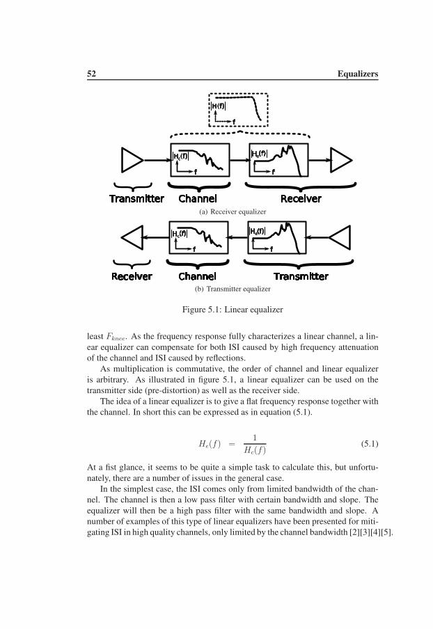
52 Equalizers
(a) Receiver equalizer
(b) Transmitter equalizer
Figure 5.1: Linear equalizer
least Fknee. As the frequency response fully characterizes a linear channel, a lin-ear equalizer can compensate for both ISI caused by high frequency attenuationof the channel and ISI caused by reflections.
As multiplication is commutative, the order of channel and linear equalizeris arbitrary. As illustrated in figure 5.1, a linear equalizer can be used on thetransmitter side (pre-distortion) as well as the receiver side.
The idea of a linear equalizer is to give a flat frequency response together withthe channel. In short this can be expressed as in equation (5.1).
He(f) =1
Hc(f)(5.1)
At a fist glance, it seems to be quite a simple task to calculate this, but unfortu-nately, there are a number of issues in the general case.
In the simplest case, the ISI comes only from limited bandwidth of the chan-nel. The channel is then a low pass filter with certain bandwidth and slope. Theequalizer will then be a high pass filter with the same bandwidth and slope. Anumber of examples of this type of linear equalizers have been presented for miti-gating ISI in high quality channels, only limited by the channel bandwidth [2][3][4][5].

5.1 Linear Equalizer 53
For a channel with ISI caused both by limited bandwidth and by reflection, thesituation is more complex. Reflections cause frequency dips that are very hard tocompensate for by filters designed in the frequency domain.
As we can model the channel as linear and time invariant, the impulse responsecan be used to calculate a good equalizer response. The signals we are interestedin consist of symbols transmitted in a time discrete sequence. Therefore, we canconsider the channel to be a time discrete channel2 characterized by a time discreteimpulse response (h(n)). For a perfect equalizer, which means an equalizer thatremoves all ISI, the impulse response of the channel (hc) and the equalizer (he)will fulfill equation (5.2).
hc(n) ∗ he(n) = δτ (n) (5.2)
Where δτ (n) is given by equation (5.3).
δτ (n) =
1 n = τ0 n 6= τ
(5.3)
In the general case, he needs to have infinite duration and be non-causal inorder to fulfill equation (5.2) even if hc is of finite length. An infinite impulse re-sponse corresponds to a FIR filter with infinite number of taps, which is somewhathard to implement in practice. Implementing a finite non-causality can be doneby introducing delay in the filter. This is a feasible solution for small delays butmay cause problems in the general case.
One way of solving the issues of an infinite and non-causal equalizer impulseresponse is to use an infinite impulse response (IIR) filter structure. This can alsoreduce the number of needed taps and thereby decrease the complexity of theequalizer implementation. There are issues with IIR filters though. The feedbacktopology of this filter structure results in a filter that might not be stable. Thestability of a filter depends on the filter coefficients. In chapter 6 we describetechniques to automatically obtain good filter coefficients for the equalizer filter.These techniques do not enable us to control the filter coefficients at all times in away that can guarantee a stable IIR filter. This issue makes linear equalizers basedon IIR filters unsuitable for the type of equalizers that are of interest in this thesis.
To make a practical equalizer possible we need to “solve” equation (5.2) forthe case when he is of finite length and where the propagation delay of the channel-equalizer system is acceptably short. There are two popular approaches to calcu-
2The time discrimination can either be done at the Nyquist rate, i.e. one time sample pertransmitted symbol or at an over-sampled rate. i.e. an integer number of samples per symbol time.In this thesis only the Nyquist rate are considered.

54 Equalizers
lating he with these restrictions. The first one uses the zero forcing criteria, whilethe second one relies on the mean-square criteria.
5.1.1 Zero Forcing
The zero forcing criteria is also called peak distortion criteria. Lets assume achannel with impulse response hc of length Lc (hc = [hc0, hc1, . . . , hc(Lc−1)]) be-ing equalized by a linear equalizer with impulse response he of length Le. Thetotal impulse response of the channel-equalizer is then h = hc ∗ he of lengthL = Lc + Le − 1.
Each term in the impulse response will then be expressed according to thedefinition of time discrete convolution as in equation (5.4).
h(m) =
Lc−1∑
j=0
hc(j) · he(m − j) (5.4)
For a system where all ISI has been eliminated, h = δτ where δτ is defined byequation (5.3). Setting h = δτ will then create one equation for each point in hwhere he are the unknowns. h is of length L = Lc + Le − 1 and he is of length Le
which gives an under-determined equation system. As such systems of equationsare only solvable in very special cases, another approach has to be used.
Let x(n) denote a transmitted signal, transmitted through a channel and a lin-ear equalizer with the combined impulse response h. The received signal z(n) isthen given by equation (5.5).
z(n) = x(n) ∗ h (5.5)
Assume that the delay in the channel and equalizer is set to τ . The convolutioncan then be written as in equation (5.6).
z(n) =τ−1∑
j=0
h(j) · x(n − j) + h(τ) · x(n − τ) +
∞∑
j=τ+1
h(j) · x(n − j) (5.6)
Here the hτ ·x(n−τ) term represents the wanted signal and the two sums representall ISI. If the data signal x consist of the symbols 1 or −1, the worst case ISI willbe given when all terms in the two sums in equation (5.6) have the same sign.Therefore, the worst case ISI can be written as in equation (5.7).

5.2 Mean-square 55
Max ISI =
∞∑
j=0,j 6=τ
|h(j)| (5.7)
Normalizing with respect to the wanted signal term in the convolution sum, we getan expression for the peak distortion in relation to the information amplitude. Thisfunction is then the peak distortion error function as in equation (5.8). Considerthis as a function of the equalizer coefficients. Minimizing this function will givean equalizer with minimum peak ISI.
J(he) =
L−1∑
m=0,m6=τ
|h(m)||h(τ)|
=L−1∑
m=0,m6=τ
|∑Lc−1j=0 hc(j) · he(m − j)|
|∑Lc−1
j=0 hc(j) · he(τ − j)|(5.8)
Even though no closed form expression has been found for the minimum ofequation (5.8) in the general case, it has been shown by Lucky in 1965 [6] thatthe function is convex. This means that the function has a global minimum andno local minima. Numerical methods can therefore be used to find the globalminimum [7].
5.2 Mean-square
The mean square criteria are also called Wiener filtering. The mean square methodfor calculating an optimum linear filter uses a statistical approach to the optimiza-tion problem.
Let x designate a signal that is transmitted over a channel with an impulseresponse hc. Denote the received signal y and the noise, added to the signal at thereceiver, v. The expression for y is then given by equation (5.9). Filter the receivedsignal by a linear equalizer with the impulse response he and the equalized signalz can be expressed according to equation (5.10).
y(n) = x(n) ∗ hc + v(n) (5.9)
z(n) = y(n) ∗ he (5.10)
Ideally, the received signal z(n) should be z(n) = x(n−τ) where τ is the channeland equalizer delay. The error ǫ in the transmission can then be expressed as thedifference shown in equation (5.11).

56 Equalizers
ǫn = x(n − τ) − z(n) (5.11)
The function that will be minimized using Wiener filters will be the square of theexpectation value of ǫ as in equation (5.12).
J = E[|ǫ|2] (5.12)
The derivation of a general solution to this problem is given in appendix C3.The result is a set of linear equations that can be solved analytically, given thechannel impulse response and the expected noise level.
The characteristics of the noise show up in these equations for the followingreason: If the channel attenuates a certain frequency band to a large extent, thenthe equalizer filter needs to amplify that frequency band substantially to compen-sate. A large amplification of a certain frequency band means that the noise in thatband will be amplified. If the noise is given in the equations, an optimum trade-offbetween ISI distortion and added noise can be found.
The filtering of the noise is a disadvantage of linear receiver equalizers. Asmultiplication and convolution is commutative, the same coefficients can be usedfor a linear transmitter equalizer. The difference is that the equalizer filter cannotfilter the noise. The coefficients for an optimum transmitter linear equalizer istherefore calculated with the noise signal set to zero.
5.3 Decision Feedback Equalizer
The structure of a DFE is shown in figure 5.2. The output of a feedback filteris subtracted from the received signal. From the difference, the information isrecovered and is used as an input to the feedback filter. The function is bestexplained in the time domain.
The linear time invariant channel can be fully characterized by an impulseresponse (see for example the impulse responses in figure 3.5 in chapter 3). TheDFE subtracts the part of the signal that comes after the main peak of the impulse,forming an equivalent channel impulse response without the “tail”. If the non-zero part of the remaining equivalent impulse response is shorter than the symboltime, then all ISI have been removed.
For a more mathematical explanation inspect figure 5.3. A signal x(n) is trans-mitted through a channel, characterized by an impulse response hc. z(n) is the
3Appendix 5.2 gives the general solution for a linear equalizer DFE combination. To calculatethe optimum coefficients for only a linear equalizer, set the length of the DFE filter to zero.

5.3 Decision Feedback Equalizer 57
Figure 5.2: Decision feedback equalizer structure
Figure 5.3: Decision feedback equalizer model

58 Equalizers
difference between the received signal y(n) and the output of a filter character-ized by the impulse response hf . The received data symbol (x) is retrieved fromz(n) by a comparator. The retrieved symbol is then used as the input signal to thefilter hf . This can be described by equations (5.13) to (5.15).
y(n) = x ∗ hc
= x(n) · hc(0) + x(n − 1) · hc(1) + x(n − 2) · hc(2) + . . . (5.13)
z(n) = y(n) − x ∗ hf (5.14)
x(n) = sign(z(n − 1)) (5.15)
Equation (5.13) and (5.14) form equation (5.16).
z(n) = x ∗ hc −x ∗ hf
= x(n) · hc(0) +x(n − 1) · hc(1) +x(n − 2) · hc(2) + . . .+−x(n) · hf (0) −x(n − 1) · hf (1) − . . .
(5.16)
Assume that the channel impulse response hc is known and that the feedback filterimpulse response parameters hf are set to hf(m) = hc(m + 1) : m = 0, 1, ....Further assume that x(n) = x(n − 1) (i.e. the transmitted signal is receivedcorrectly). Then equation (5.16) is reduced to equation (5.17).
z(n) = x(n) · hc(0) (5.17)
As shown in equation (5.17), the comparator input signal z(n) does only de-pend on x(n) at time index n and no other time index. This is the same as sayingthat the ISI has been removed. The equations point out another important charac-teristic of the DFE algorithm. Equation (5.16) will be reduced to equation (5.17)only if we know the channel characteristics hc and if the transmitted signal is re-ceived correctly. Furthermore, the signal that is sent to the detector4 is the sentsignal scaled with hc(0). If hc(0) is small, then the detector receives a small sig-nal and is then sensitive to noise. The DFE is therefore not suitable for all typesof channels. A channel where the impulse response amplitude increases gradu-ally will have a so-called pre-cursor that will cause either a very noise sensitivereceiver or a DFE implementation that cannot remove the ISI caused by the pre-cursor. A combination of a linear equalizer and a DFE, described in the next sec-tion can be used to efficiently handle pre-cursors. For a multi-drop a DRAM bus,the channel impulse response generally do not have any pre-cursor (see figure 3.5as an example) and a pure DFE is therefore an attractive approach to enable higherdata-rates.
The feedback structure of the DFE has both advantages and disadvantages.The symbol decision comparator is a non-linear function that removes the noise
4The detector here means the block that recovers the digital symbols.

5.4 Linear Equalizer and DFE Combinations 59
from the signal. Using the decided symbol (x) as the input to the feedback filterensures that the output signal of filter hf does not add noise to the input signal.
The two main disadvantages also relate to the feedback. First, the ISI can onlybe removed if the signal is received correctly. If a symbol is misinterpreted, theincorrect symbol will be fed back to the input signal through the filter hf and thecomparator input will contain ISI. This error feedback can result in so-called bursterrors. One incorrectly received symbol will result in errors in the following sym-bol interpretations and a whole burst of errors may appear. A second disadvantagewith the DFE is the time critical feedback loop. The comparator input signal attime index n is a function of the comparator result at time index n − 1. Thistime critical timing loop sets severe constraints on high-speed DFE implementa-tions. Among the techniques that enable high-speed algorithm implementations,pipelining is out of question. Only unfolding can be used at the expense of extrahardware. A more detailed description of DFE implementation considerations canbe found in chapter 7.
5.4 Linear Equalizer and DFE Combinations
The combination of a linear equalizer and a DFE can sometimes be an attractivesolution. The structure of such a combination can be seen in figure 5.4(a). Thefunction of this structure is expressed in equation (5.18). The linear filter canhandle any pre-cursor in the channel impulse response and the noise suppressingproperties of the DFE can be exploited for the non pre-cursor part of the equaliza-tion.
z(n) = x(n) ∗ he ∗ hc − x(n) ∗ hf (5.18)
As two equalizer filters are used, the task of setting optimum coefficients forthe filter gets more complex. If transmission errors are neglected, Wiener filterscan be used also for the combined equalizer structure. If there are no transmissionerrors5, then x(n) = x(n − τ). The linear model shown in figure 5.4(b) will thencharacterize the system, as expressed in mathematical terms in equation (5.19).As in section 5.2, the error signal can then be expressed as in equation (5.11) andminimizing the error function in equation (5.12) will give the filter coefficients forthe two filters. The derivation of the coefficients is given in appendix C.
z(n) = x(n) ∗ he ∗ hc − x(n − τ) ∗ hf (5.19)
5If we do not use this assumption, the analysis of the equalizer will be extremely difficult(see [8]). On the other hand if this assumption is not valid we have an equalizer which does notperform and is therefore not very interesting to use in the system.

60 Equalizers
(a) Linear, DFE combination
(b) Linear model
Figure 5.4: Linear and DFE equalizer
References
[1] H. Nyquist, “Certain topics on telegraph transmission theory,” Transactions
of the A.I.E.E., pp. 617–644, February 1928. Reprinted in: Proceesings ofIEEE, vol. 90, No. 2, February 2002.
[2] J. Lee, “A 20-Gb/s Adaptive Equalizer in 0.13-µm CMOS Technology,” IEEE
Journal of solid-state circuits, vol. 41, pp. 2058–2066, September 2006.
[3] Y. Tomita, M. Kibune, J. Ogawa, W. W. Walker, H. Tamura, and T. Kuroda, “A10Gb/s Receiver with Equalizer and On-chip ISI Monitor in 0.11µm CMOS,”in IEEE Symposium on VLSI Circuits, Digest of Technical Papers, pp. 202–205, 2004.
[4] S. Gondi, J. Lee, D. Takeuchi, and B. Razavi, “A 10Gb/s CMOS AdaptiveEqualizer for Backplane Applications,” in IEEE International Solid-State Cir-
cuits Conference, Digest of Technical Papers, pp. 328–329, February 2005.
[5] G. Zhang, P. Chaudhari, and M. M. Green, “A BiCMOS 10Gb/s Adaptive Ca-ble Equalizer,” in IEEE International Solid-State Circuits Conference, Digest
of Technical Papers, pp. 482–483, February 2004.
[6] R. W. Lucky, “Automatic Equalization for Digital Communication,” The Bell
System Technical Journal, vol. 44, pp. 547–588, 1965.

5.4 Linear Equalizer and DFE Combinations 61
[7] J. G. Proakis, Digital Communications. McGray-Hill, 2001.
[8] S. Hasnie, Modified Decision Feedback Equalization Techniques for Data
Communications. PhD thesis, The Austrialian National University, March1999.

62 Equalizers

Chapter 6
Equalizer Adaptation
6.1 Gain Channel Knowledge
In chapter 5, the channel characteristics hc were assumed to be known. In general,this is not the case. In this chapter, we will discuss how to acquire informationabout the channel characteristics needed for equalization. Two main techniqueswill be discussed: training sequences and blind adaptation.
6.2 Training Sequence
The idea of the training sequence technique is to transmit a known sequence overthe channel and from the distortion of the signal extract the channel characteris-tics. This can be done either by mathematical estimation of the channel parametersor by an iterative process.
6.2.1 Channel Extraction
For a linear time-invariant channel, the impulse response fully characterizes thechannel. From the definition of convolution we can express a sequence of receivedsignals y as a function of transmitted signals x and the channel impulse responsehc. If the channel is modeled by p + 1 coefficients and if m + 1 received symbolsare used, the relationship between the transmitted symbols, the channel impulseresponse and the received symbols can be expressed as a set of linear equations asin (6.1).
63

64 Equalizer Adaptation
y(n) = x(n)hc(0)+ x(n − 1)hc(1) + · · ·+ x(n − p)hc(p)y(n + 1) = x(n + 1)hc(0)+ x(n)hc(1) + · · ·+ x(n − p + 1)hc(p)
... =...
...y(n + m) = x(n + m)hc(0)+ x(n + m − 1)hc(1) + · · ·+ x(n − p + m)hc(p)
(6.1)If the transmitted and received sequences are known, the equations can be
solved for hc. The number of received symbols is in general greater than thechannel impulse response length in order to minimize the sensitivity to noise. Forthis case, (6.1) forms an over-defined set of linear equations. Least mean squareprojection can then be used to estimate the channel.
Writing equation (6.1) in matrix form gives equation (6.2). Where M is a(m + 1) × (p + 1) matrix.
Y = MHc (6.2)
From this we can estimate the channel impulse response using least square pro-jection as in equation (6.3) [1].
Hc =(
MTM)−1
MY (6.3)
When the estimated channel response Hc has been calculate, optimum equal-izer coefficients can be calculated as described in chapter 5. It can be shown thatthe estimated error covariance of the channel response is given by Cov(Hc) =(MT
M)−1. M is only a function of x. In order to have a good estimate we mustchoose a training sequence x that gives a minimum error covariance.
From equation (6.3) we see that the channel estimate is a matrix multiplicationof a matrix,
(
MTM)−1
M, and the received signal Y when the training sequence
is transmitted. This can be seen as a matched filter from Y to Hc.
6.2.2 Iterative Equalizer Adjustment
The use of a technique that is simple enough to be implemented in hardware wasfirst suggested by Lucky in 1965 [2]. The paper suggests transmitting a set oftraining impulses and uses a series of counters to gradually set the linear equalizercoefficients to the correct values. The algorithm is based on zero forcing criteria.However, the algorithm enables efficient equalizer implementation but it suffersin our field of interest from a critical flaw. The algorithm can only guaranteeconvergence for the case where the ISI is small enough not to close the eye. That

6.2 Training Sequence 65
means that the error function in equation (5.8) is less than 1. For multi-dropchannels with severe ISI, this condition can not be guaranteed.
After Lucky, a number of alternative algorithms have been suggested. Accord-ing to [3] the adaptive least mean square (LMS) algorithm was developed by B.Widrow in 1966, and 1970. A version based on Kalman filters was presented byD. Godard in 1974 [4].
Appendix C describes how to minimize the LMS error if the channel charac-teristics are known. This section describes how to achieve this minimization usingan iterative approach.
The error function J as defined by equation (C.6). To iteratively retrieve aminimum error J start with a set of equalizer parameters~h0
ef = [h0e(0), h0
e(1), . . . , h0e(Le − 1), h0
f(0), . . . , h0f(Lf − 1)]. At this point the
error function will have a certain value J0 = J(~h0ef). To reduce J , the algorithm
of steepest descent can be used. By repeated small steps in the ~hef space in thedirection that makes J decrease the most, J can be minimized. This direction isdefined as minus the gradient of J (notation − J(~hef)). Using the step size (µ)the coefficients will be updated according to equation (6.4).
~h(j+1)ef = ~hj
ef − µ · J(~hnef) (6.4)
The gradient of J can be expressed as the partial derivatives of J with respect tohef as in equation (6.5).
J(~he) =
∂J∂he(0)
∂J∂he(1)
...∂J
∂he(Le−1)∂J
∂hf (0)...
∂J∂hf (Le−1)
(6.5)
From equation (C.7) and (C.8) we can rewriteJ(~he) according to equation (6.6).

66 Equalizer Adaptation
J(~he) = 2
−E [ǫ · y(n − 0)]−E [ǫ · y(n − 1)]
...−E [ǫ · y(n − Le + 1)]E [ǫ · x(n − 0 − τ − 1)]
...E [ǫ · x(n − (Lf − 1) − τ − 1)]
(6.6)
Equation (C.9) and (C.10) show that E [ǫ · y(n − k)] and E [ǫ · x(n − k − τ − 1)]depend on the autocorrelation functions Rxy and Ryy, which according to equa-tions (C.21) and (C.22) depend on the channel impulse response hc. As the ideaof adaptive equalization is to obtain a good equalizer without prior knowledge ofthe channel impulse response (hc), E [ǫ · y(n − k)] and E [ǫ · x(n − k − τ − 1)]have to be estimated in a different way.
A simple estimation of E [ǫ · y(n − k)] at time n is ǫ · y(n − k). Using thisestimate, the steepest decent coefficient updating in equation (6.4) will for he bewritten according to equation (6.7). In the same way, the algorithm for updatinghf is shown in equation (6.8).
h(j+1)e (k) = hj
e(k) + 2µ · ǫ · y(n − k) (6.7)
h(j+1)f (k) = hj
f(k) − 2µ · ǫ · x(n − k − τ − 1) (6.8)
This algorithm offers very efficient hardware implementations. Figure 6.1 showsone implementation of this algorithm. To reduce the complexity of the algorithmeven further [3], it is possible to use the sign of the error signal ǫ and/or x/y.Equations (6.7) and (6.8) can then be modified as in equations (6.9) to (6.14).
h(j+1)e (k) = hj
e(k) + 2µ · sign(ǫ) · y(n − k) (6.9)
h(j+1)e (k) = hj
e(k) + 2µ · ǫ · sign(y(n − k)) (6.10)
h(j+1)e (k) = hj
e(k) + 2µ · sign(ǫ) · sign(y(n − k)) (6.11)
h(j+1)f (k) = hj
f(k) − 2µ · sign(ǫ) · x(n − k − τ − 1) (6.12)
h(j+1)f (k) = hj
f(k) − 2µ · ǫ · sign(x(n − k − τ − 1)) (6.13)
h(j+1)f (k) = hj
f(k) − 2µ · sign(ǫ) · sign(x(n − k − τ − 1)) (6.14)
The reduction of complexity comes at a cost. The updating step length will notgo to zero if sign(ǫ) is used. The coefficients will oscillate around the optimum
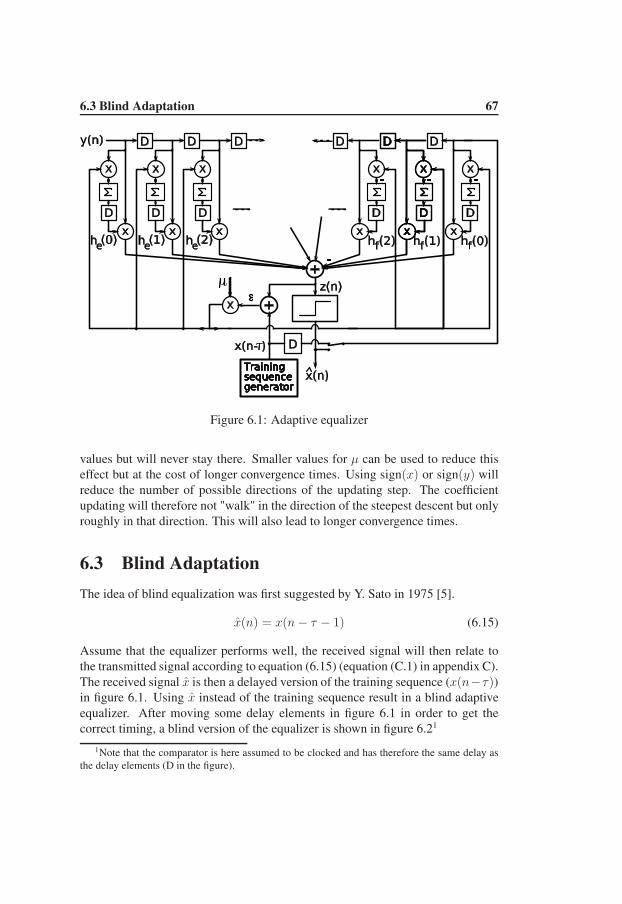
6.3 Blind Adaptation 67
Figure 6.1: Adaptive equalizer
values but will never stay there. Smaller values for µ can be used to reduce thiseffect but at the cost of longer convergence times. Using sign(x) or sign(y) willreduce the number of possible directions of the updating step. The coefficientupdating will therefore not "walk" in the direction of the steepest descent but onlyroughly in that direction. This will also lead to longer convergence times.
6.3 Blind Adaptation
The idea of blind equalization was first suggested by Y. Sato in 1975 [5].
x(n) = x(n − τ − 1) (6.15)
Assume that the equalizer performs well, the received signal will then relate tothe transmitted signal according to equation (6.15) (equation (C.1) in appendix C).The received signal x is then a delayed version of the training sequence (x(n−τ))in figure 6.1. Using x instead of the training sequence result in a blind adaptiveequalizer. After moving some delay elements in figure 6.1 in order to get thecorrect timing, a blind version of the equalizer is shown in figure 6.21
1Note that the comparator is here assumed to be clocked and has therefore the same delay asthe delay elements (D in the figure).

68 Equalizer Adaptation
Figure 6.2: Blind adaptive equalizer
The only difference compared to the iterative approach in the previous sectionis the estimation of the error signal ǫ. For a blind equalizer the non-linearity ofthe comparator defines the error. If there is higher probability that the compara-tor output signal is correct than wrong, then there is a higher probability that thecoefficients will take a step towards the optimum value than in any other direc-tion. Thus, it is likely that the equalizer coefficients eventually reach the optimumvalue.
The initial values of the coefficients are critical for the convergence of theequalizer. This is especially important for the DFE part of an equalizer as it byitself has a feedback loop. Here, using small values for µ helps as it will averageout steps in the wrong direction. To use the sign of the error or the data (x andy) to simplify implementation works just as good for a blind equalizer as for thetraining sequence case. Implementations of blind sign-sign DFEs are presented inchapter 10. Measurement results presented in the chapter show descent conver-gence properties also for channels with severe distortion and consequently highprobability for initial transmission errors.
As blind adaptation can be performed on actual data, the algorithm can contin-uously track slow changes of the channel characteristics. Interruption of normaltransmission and higher-level protocols to control periods of training sequencetransmission is therefore not necessary.
If the blind adaptation is active continuously, the convergence speed is not that

6.4 Data Dependent Convergence 69
critical. The multiplication factor µ can then be set to a small value. The unwantedeffects on using simplified sign representation can then kept to a minimum. Ac-cepting long convergence times also enables simplification of the updating logic.For high data rates, the calculation of the error, multiplication by µ and summa-tion can be an implementation challenge. If z, ~x, and ~y are sampled and stored,the calculation of a new set of coefficients can be done at an arbitrary pace.
6.4 Data Dependent Convergence
Recall from section 6.2.1 that the estimation error depends on the training se-quence used. Correspondingly, this is also true for iterative adaptation. Goodestimations of E [ǫ · y(n − k)] and E [ǫ · x(n − k − τ − 1)] are needed for a truesteepest descent algorithm. The used ǫ ·y(n−k) and ǫ ·x(n−k−τ −1) are fairlyrough estimations of E [ǫ · y(n − k)] and E [ǫ · x(n − k − τ − 1)]. One can seethe simplification as instead of walking in the steepest descent direction in the hef
space, there is the choice of walking either up-hill or down-hill in a direction setby current values of ~y and ~x. If the values for ~y and ~x remains constant, there isa very little chance that steps in the directions available will end up at the lowestpoint in the hef space.
If a training sequence is used, that sequence can be chosen to ensure that therewill be a variety of possible directions to take steps in. If blind adaptation is used,there are implementations that stop walking if the ~y and ~x vectors remain fixed ordo not have sufficient variation (see section 8.5.6 in chapter 8). This will minimizethe effects of the crude approximation of the expectation value.
References
[1] F. Gustafsson, L. Ljung, and M. Millnert, Signalbehandling. Studentlitteratur,2001.
[2] R. W. Lucky, “Automatic Equalization for Digital Communication,” The Bell
System Technical Journal, vol. 44, pp. 547–588, 1965.
[3] J. G. Proakis, Digital Communications. McGray-Hill, 2001.
[4] D. Godard, “Channel Equalization Using a Kalman Filter for Fast Data Trans-mission,” IBM J. Res. Develop, pp. 267–273, 1974.
[5] T. Sato, “A Method of Self-Recovering Equalization for MultilevelAmplitude-Modulation Systems,” IEEE Transactions on communications,pp. 679–682, 1975.

70 Equalizer Adaptation

Chapter 7
Equalizer Design
The use of equalization is only meaningful if it enables higher data transmissionrates. For DRAM-buses that means that equalization has to be performed in theGb/s range to provide any improvement in bit rates. It is not trivial to implementequalizers for these high speeds. This chapter presents implementation strategiesfor high-speed equalization circuits.
7.1 Analog High Frequency Boosting
When investigating literature for high-speed equalizers, the implementations thatreport the highest data rates are fully analog, as 20 Gb/s in [1], 10 Gb/s in [2, 3, 4].Typically, these high-speed implementations aim to mitigate ISI caused by limitedchannel bandwidth only. As the channel attenuates high frequencies, this meansthat the equalizer amplifies high frequency signals, extending the flat frequencyresponse up in frequency. To achieve good equalization, these equalizers needto match the low pass cut off frequency of the channel with the high pass cutoff frequency of the equalizer. For adaptation, they basically change the cut offfrequency (fz) as illustrated in figure 7.1. For a channel that does not fit a one-pole system, [1] and [2] use two cascaded high pass stages where the zero of eachstage can be moved independently. In [3] five stages are used.
Though the analog approach enables very high-speed implementations, theability to adapt to channel distortion is limited. If adaptation to more complexchannel distortion is needed, different structures have to be considered (or com-binations of frequency boosting and other structures as in [5]). If individual filtertap adjustment is needed, literature show a number of mixed analog and digitalstructures.
71

72 Equalizer Design
Figure 7.1: Variable bandwidth receiver equalizer
7.2 Linear Mixed Signal Receiver Equalizer
For linear receiver equalizers, the input signal is analog and the contribution ofall filter taps has to be summed before a symbol decision can be made. Thismeans that the equalizer either has to handle analog signals all the way to thecomparator or convert the input signal into the digital domain and perform theequalization in the digital domain. High speed equalizer implementation usingdirect sampling have been reported [6] but most frequently used structures doesinstead use variable gain stages in each filter tap where the gain is proportionalto the filter tap coefficient. Published high-speed implementations use differentkinds of multiplying DACs (MDACs) for this functionality.
A linear receiver equalizer for up to 8 Gb/s is presented in [7, 8]. The paperspresent a time discrete equalizer with five individually programmable taps. By us-ing eight time-interleaved equalizers, the speed requirements of each equalizer arerelaxed. The gain in each filter tap is controlled by a digital word in a multiplyingDAC (MDAC) implemented as current switches. In [9] a time continuous FIR fil-ter is used as a linear receiver equalizer. Each filter tap consists of an analog delayelement and an MDAC. These amplify the input signal by a value determined by adigital input word. The input word is then the filter coefficient. In [9] the MDACis implemented using switchable current mirrors. Though the structure enables a

7.3 Linear Transmitter Equalizer and DFE 73
Figure 7.2: Mixed signal transmitter equalizer
highly configurable linear receiver equalizer the maximum transmission rate in [9]is limited to 1 Gb/s.
7.3 Linear Transmitter Equalizer and DFE
7.3.1 Switched DAC Output
For linear transmitter equalizers and for decision feedback equalizers, here calledthe switched DAC approach, is reported frequently in literature. This structureexploits the fact that the input signal to a linear transmitter equalizer consists ofdigital symbols. The input signals to a linear transmitter equalizer, as well as toa DFE, have the same width as the data. For the systems of interest here, thatmeans a stream of ones and zeros. Multiplication of the input signal and thecoefficients in the convolution sum will then reduce to adding or subtracting thecoefficients. This enables an implementation whereby the filter coefficient he isconverted to an analog signal (usually a current) and switched between the positiveand negative output nodes y depending on the data signal x, as shown in figure 7.2.The DAC output can drive the output signal directly, or the DAC can control thedriving strength of a buffer that is switched between the output nodes. Recall fromsection 5.3 that the filter used in a receiver DFE has the received signal (x) as inputsignal, which has the same width as the transmitted signal. The same type of filterimplementation can therefore be used for a DFE as well.
For example [5] and [10] use a version of this structure for both linear trans-mitter equalizers and receiver DFEs. They are reporting data rates of 6.4 Gb/s and10 Gb/s respectively. PAM-4 implementations with both linear transmitter equal-izer and DFE utilizing this principle for up to 10 Gb/s are described in [11, 12]. Atime interleaved DFE for up to 2 Gb/s with this structure is presented in [13].

74 Equalizer Design
Figure 7.3: RAM-DFE principle
Having one DAC per tap has both advantages and disadvantages. The speedrequirements of the DACs are very moderate with this solution as the coefficientschange very little and slowly over time. Multiplication by ±1 can be implementedefficiently and at high-speed. A disadvantage is that each filter tap loads the sum-mation node. That means that for increasing number of filter taps, the summationnode will encounter more and more parasitic load. This will reduce the bandwidthof that node. In both [12] and [5] the filter tap buffers have been scaled so that allequalizer coefficients do not have the same range. This is done to reduce parasiticsat the summation node.
7.3.2 RAM-DFE
Another implementation structure is the so called RAM-DFE. Here the wholeconvolution sum (x ∗ c) is stored in a memory, a look-up table. The received datais then used to address the sum which is subtracted from the input signal as in allDFE implementations (see figure 7.3). [14] uses an analog RAM memory, oper-ating up to 200 Mb/s. In [15] a digital 6 bit RAM memory is used in combinationwith a high-speed DAC operating at 90 Mb/s.
In a RAM-DFE one value is saved for each combination of input signals. Thismakes it possible to compensate not only for linear distortion (distortion that canbe characterized by the channels impulse response) but also for non-linear effects.

7.4 Trading Hardware for Speed 75
The main drawback is that the memory size is proportional to two to the power ofthe equalizer length, making the memory size infeasible for long equalizers.
For adaptive implementations, the RAM-DFE structure suffers from longerconvergence times compared to other implementation structures since each RAMcell is adapted individually compared to adaptation of each filter coefficient inother structures.
7.4 Trading Hardware for Speed
To improve the performance of an equalizer implementation there is often the pos-sibility to trade extra hardware for transmission speed. The two main techniquesto do this is unfolding and look ahead.
7.4.1 Unfolding
Unfolding1 is basically adding extra copies of computational blocks and distribut-ing the tasks between them. This way the total amount of work that can beperformed is increased, enabling higher data-rates. Theoretically, unfolding canachieve arbitrary computation speeds as long as there are no signal loops in thesystem. For algorithms with loops such as DFE structures, the loops limits theusability of unfolding. However, there are a number of high-speed equalizer im-plementations that use unfolding.
As examples of the publications referred to in this chapter: Jaussi et. al. [7, 8]unfold their mixed signal linear equalizer by a factor of eight; Ieressel et. al. [13]presents a factor of four unfolded DFE implementation; Sohn et. al. [16, 17, 18]unfold the one DFE tap in the receiver and so do also Bae et. al. in [19].
The equalization implementations described in chapter 8 and in more detail inchapter 10 use a factor two unfolding for the comparator and DAC parts.
7.4.2 Look-ahead
Look-ahead implementations use multiple computing units to perform the sametask with different input data and choose the correct result afterwords. The tech-nique can be used to relax feedback loop timing constraints in DFEs as for in-stance in [19]. [20] describe a DFE structure that use look-ahead to its full extent.The paper suggest one comparator for each possible combination of DFE filterinput signals and then select the correct result in a tree structure. The structureenables compensation for non-linear effects in the same way as the RAM-DFE in
1The term interleaved are also used to describe the same type of implementation technique.For the circuits described here the terms are synonymous.
76 Equalizer Design
section 7.3.2. The complexity of the structure scales as two to the power of thefilter length which means that the structure is not suitable for long filters.
7.5 Adaptation
Chapter 6 describes techniques to adjust equalizer parameters in order to mitigateISI in an optimal way. The implementation of these techniques depend on theequalizer structure used. For analog high frequency boosting equalizers describedin section 7.1, the number of parameters to adjust is small. This opens for simpleand efficient adaptation implementation. In [1] and [3], the equalizer is adjusteddepending on the frequency content of the equalized signal. By comparing the sig-nal power of high frequencies and low frequencies, [1] can adjust the equalizationto be optimal.
For equalizer structures based on FIR filter tap adjustment (as in section 7.3.1)the LMS adaptation algorithm is the most popular [5, 7, 8, 10]. [12] suggest amethod to adjust not only the receiver equalizer but also a transmitter equalizer.The idea is to transmit error information back to the transmitter by using the com-mon mode signal on the presented differential channel.
7.6 Multi-drop Bus Equalizers
The majority of publications on high speed equalization circuits address point-to-point communication. Publications that address ISI on multi-drop buses arerelatively few. A 1-tap DFE is presented in [16, 17, 18] which partially mitigatesthe ISI. [19] presents a 2Gb/s 2-tap DFE implementation for multi-drop buses.[21] presents a one tap DFE for 3 Gb/s operation on a 4-drop bus and [22] presentsa one tap DFE for 3.2 Gb/s operating on a 2-drop bus. All these implementationscan only remove ISI partially for multi-Gb/s transmissions on multi-drop buses.The target scenario in this thesis is communication at several Gb/s over a multi-drop buses with a large number of endpoints. The length of the impulse responsefor such a channel is in the order of 4 ns to 10 ns (see figure 3.5 in section 3.3as an example). Long filters are therefore needed to mitigate all ISI over such achannel. The equalizers in this thesis aim to mitigate a larger proportion of the ISIand the filter length proposed here is therefore substantially longer compared topreviously presented equalizers for multi-drop buses.

7.6 Multi-drop Bus Equalizers 77
Figure 7.4: Proposed DFE structure
7.6.1 Proposed Structure
The proposed equalizer structure is shown in figure 7.4. The structure is a com-bination of the switched DAC structure described in section 7.3.1 and the RAM-DFE structure in section 7.3.2. If the weights of the DACs in figure 7.2 are powersof two and the switches are controlled by an arbitrary input signal instead of thedelayed input signal, the equalizer structure basically converts into a DAC. Thenumber of taps in the DFE structure will then correspond to the word length ofthe DAC. Switched DAC DFE equalizers for several Gb/s operation have reportedwith more than five taps [10, 23]. To implement DACs for several Gb/s with wordlengths of at least 5 bits should therefore be fully feasible. By analogy, the tapcoefficients of the DAC are fixed which enables scaling of the design to minimizeparasitic effects in the same manner as in [5] and [12].
The input to the DAC could be the output from a RAM as in section 7.3.2.As the aim is to have a large number of filter coefficients, the RAM approachwould give an impractically large memory. The proposed structure performs filterconvolution operations in a FIR filter instead of memory lookup. With the onebit input signal, this can be implemented in an efficient way at high speed. Theimplementation of the structure will be further described in the next chapter.
References
[1] J. Lee, “A 20-Gb/s Adaptive Equalizer in 0.13-µm CMOS Technology,”IEEE Journal of solid-state circuits, vol. 41, pp. 2058–2066, September2006.
[2] Y. Tomita, M. Kibune, J. Ogawa, W. W. Walker, H. Tamura, and T. Kuroda,“A 10Gb/s Receiver with Equalizer and On-chip ISI Monitor in 0.11µm

78 Equalizer Design
CMOS,” in IEEE Symposium on VLSI Circuits, Digest of Technical Papers,pp. 202–205, 2004.
[3] S. Gondi, J. Lee, D. Takeuchi, and B. Razavi, “A 10Gb/s CMOS AdaptiveEqualizer for Backplane Applications,” in IEEE International Solid-State
Circuits Conference, Digest of Technical Papers, pp. 328–329, February2005.
[4] G. Zhang, P. Chaudhari, and M. M. Green, “A BiCMOS 10Gb/s AdaptiveCable Equalizer,” in IEEE International Solid-State Circuits Conference, Di-
gest of Technical Papers, pp. 482–483, February 2004.
[5] M. Sorna, T. Beukema, K. Selander, S. Zier, B. Ji, P. Murfet, J. Mason,W. Rhee, H. Ainspan, and B. Parker, “A 6.4Gb/s CMOS SerDes Core withFeedforward and Decision-Feedback Equalization,” in IEEE International
Solid-State Circuits Conference, Digest of Technical Papers, vol. 1, pp. 62–63, February 2005.
[6] M. Harwood, N. Warke, R. Simpson, T. Leslie, A. Amerasekera, S. Batty,D. Colman, E. Carr, V. Gopinathan, S. Hubbins, P. Joy, P. Khandelwal,B. Killips, T. Krause, S. Lytollis, A. Pickering, M. Saxton, D. Sebastio,G. Swanson, A. Szczepanek, T. Ward, J. Williams, R. Williams, and T. Will-werth, “A 12.5Gb/s SerDes in 65nm CMOS Using a Baud-Rate ADC withDigital Receiver Equalization and Clock Recovery,” in IEEE International
Solid-State Circuits Conference, 2007 Digest of Technical Papers., pp. 436–591, 2007.
[7] J. E. Jaussi, G. Balamurugan, D. R. Johnson, B. K. Casper, A. Martin, J. T.Kennedy, N. Shanbhag, and R. Mooney, “An 8Gb/s Source-Synchronous I/OLink with Adaptive Receiver Equalization, Offset Cancellation and ClockDeskew,” in IEEE International Solid-State Circuits Conference, Digest of
Technical Papers, vol. 1, pp. 246–247, 2004.
[8] J. E. Jaussi, G. Balamurugan, D. R. Johnson, B. K. Casper, A. Martin, J. T.Kennedy, N. Shanbhag, and R. Mooney, “8Gb/s Source-Synchronous I/OLink With Adaptive Receiver Equalization, Offset Cancellation and ClockDe-Skew,” IEEE Journal of solid-state circuits, vol. 40, pp. 80–88, January2005.
[9] X. Lin, S. Saw, and J. Liu, “A CMOS 0.25-µm Continuous-Time FIR FilterWith 125 ps per Tap Delay a Fractionally Spaced Receiver Equalizer for1-Gb/s Data Transmission,” IEEE Journal of solid-state circuits, vol. 40,pp. 593–602, March 2005.

7.6 Multi-drop Bus Equalizers 79
[10] M. Meghelli, S. Rylov, J. Bulzacchelli, W. Rhee, A. Rylyakov, H. Ainspan,B. Parker, M. Beakes, A. Chung, T. Beukema, P. Pepeljugoski, L. Shan,Y. Kwark, S. Gowda, and D. Friedman, “A 10Gb/s 5-Tap-DFE/4-Tap-FFETransceiver in 90nm CMOS,” in IEEE International Solid-State Circuits
Conference, 2006 Digest of Technical Papers., pp. 80–81, 2006.
[11] J. L. Zerbe, C. W. Werner, V. Stojanovic, F. Chen, J. Wei, G. Tsang, D. Kim,W. F. Stonecypher, A. Ho, T. P. Thrush, R. T. Kollipara, M. A. Horowitz,and K. S. Donnelly, “Equalization and Clock Recovery for a 2.5-10Gb/s 2-PAM/4-PAM Backplane Transceiver Cell,” IEEE Journal of solid-state cir-
cuits, vol. 38, pp. 2121–2130, December 2003.
[12] V. Stojanovic, A. Ho, B. W. Garlepp, F. Chen, J. Wei, G. Tsang, E. Alon,R. T. Kollipara, C. W. Werner, J. L. Zerbe, and M. A. Horowitz, “Au-tonomous Dual-Mode (PAM2/4) Serial Link Transceiver With AdaptiveEqualization and Data Recovery,” IEEE Journal of solid-state circuits,vol. 40, pp. 1012–1026, April 2005.
[13] M. van Ierssel, J. Wong, and A. Sheikholeslami, “An Adaptive 4-PAMDecision-Feedback Equalizer for Chip-To-Chip Signaling,” in IEEE Inter-
national SOC Conference, 2004. Proceedings., pp. 297–300, 2004.
[14] N. P. Sands, M. W. Hauser, G. Liang, G. Groenewold, S. Lam, C.-H. Lin,J. Kuklewicz, L. Lang, and R. Dakshinamurthy, “A 200Mb/s Analog DFERead Channel,” in IEEE International Solid-State Circuits Conference, Di-
gest of Technical Papers, pp. 72–73, February 1996.
[15] B. C. Rothenberg, J. E. C. Brown, P. J. Hurst, and S. H. Lewis, “A mixed-Signal RAM Decision-Feedback Equalizer for Disk Drives,” IEEE Journal
of solid-state circuits, vol. 32, pp. 713–721, May 1997.
[16] Y.-S. Sohn, S.-J. Bae, H.-J. Park, and S.-I. Cho, “A 1.2 Gbps CMOS DFE re-ceiver with the extended sampling time window for application to the SSTLchannel,” in Symposium on VLSI Circuits Digest of Technical Papers, pp. 92–93, June 2002.
[17] Y.-S. Sohn, S.-J. Bae, and H.-J. Park, “A 1.35Gbps decision feedback equal-izing receiver for the SSTL SDRAM interface with 2X over-sampling phasedetector for skew compensation between clock and data,” in Proceedings of
the 28th European Solid-State Circuits Conference, pp. 787–790, September2002.
[18] Y.-S. Sohn, S.-J. Bae, H.-J. Park, and S.-I. Cho, “A Decision FeedbackEqualizing Receiver for the SSTL SDRAM Interface with Clock-Data

80 Equalizer Design
Skew Compensation,” IEICE TRANSACTIONS on Electronics, vol. E87-C,pp. 809–817, May 2004.
[19] S.-J. Bae, H.-J. Chi, Y.-S. Sohn, and H.-J. Park, “A 2 Gb/s 2-tap DFE re-ceiver for multi-drop single-ended signaling systems with reduced noise,”in IEEE International Solid-State Circuits Conference, Digest of Technical
Papers, vol. 1, pp. 244–245, 2004.
[20] S. Kasturia and J. H. Winters, “Techniques for high-speed implementationof nonlinear cancellation,” IEEE Journal on Selected Areas in Communica-
tions, vol. 9, pp. 771–717, June 1991.
[21] S.-J. Bae, H.-J. Chi, H.-R. Kim, and H.-J. Park, “A 3Gb/s 8b single-endedtransceiver for 4-drop DRAM interface with digital calibration of equaliza-tion skew and offset coefficients,” in IEEE International Solid-State Circuits
Conference, Digest of Technical Papers, vol. 1, pp. 520–521, 2005.
[22] H.-J. Chi, J.-S. Lee, S.-H. Jeon, S.-J. Bae, J.-Y. Sim, and H.-J. Park, “A3.2Gb/s 8b Single-Ended Integrating DFE RX for 2-Drop DRAM Interfacewith Internal Reference Voltage and Digital Calibration", a 3gb/s 8b single-ended transceiver for 4-drop dram interface with digital calibration of equal-ization skew and offset coefficients booktitle =,”
[23] B. S. Leibowitz, J. Kizer, H. Lee, F. Chen, A. Ho, M. Jeeradit, A. Bansal,T. Greer, S. Li, R. Farjad-Rad, W. Stonecypher, Y. Frans, B. Daly, F. Heaton,B. W. Garlepp, C. W. Werner, N. Nguyen, V. Stojanovic, and J. L. Zerbe,“A 7.5 Gb/s 10-Tap DFE Receiver with First Tap Partial Response, Spec-trally Gated Adaptation, and 2nd-Order Data-Filtered CDR,” in IEEE Inter-
national Solid-State Circuits Conference, 2007 Digest of Technical Papers.,pp. 228–229, 2007.

Chapter 8
Implemented Equalizers
A substantial part of the work, that eventually has resulted in this thesis, has beenspent on designing two test chips. Both test chips comprise a mixed signal DFEwith blind adaptation and evaluation blocks. Chip-organization and measurementresults are presented in chapter 10. Evaluation of the first test chip showed thattiming issues due to high fan-out of the comparator output nodes limited the per-formance to such a degree that the proof of several Gb/s over a multi-drop bus witha large number of endpoints was not possible. A redesign of the filter structuresolved this problem for the second test chip. The structure and implementationdetails are described in this chapter.
8.1 Overall Structure
The overall structure of the implemented equalizers is shown in figure 8.1. Theinput signal V in is received at an input stage (IS) which performs channel termi-nation and converts the single signal line input voltage to three differential currentsand is described in section 8.2. The currents are distributed to three identical front-end blocks (FE). Each of these consists of three parts: A look-ahead filter blockthat implements two filter taps and digital offset compensation (see section 8.4.1and section 8.5), a DAC which is designed to handle the carry-save data repre-sentation that is used in the filter (see section 8.4.4), and a differential clockedcomparator (see section 8.3).
The look-ahead filters in all three blocks are fed by one single digital filter.The filter coefficients in all these filters are controlled by an adaptation, control,and IO-interface block (see section 8.5).
81

82 Implemented Equalizers
Figure 8.1: Implemented DFE structure
8.2 Analog Input Stage
The input signal to the equalizer is the voltage at the data receiver pin. The mostconvenient and efficient way of implementing a high-speed DAC is to use a dif-ferential current steering structure. High-speed comparators are also preferablyimplemented using differential structures. It is also very attractive to performsummation of high bandwidth analog signals as differential current summation inlow impedance nodes. All in all, there are a number of good reasons for convertingthe single-ended input voltage to differential currents.
As described in section 3.2, the termination impedances can have significantinfluence on the channel characteristics. From section 3.4, we see that a welldefined termination impedance is also needed in order to utilize the reciprocitytheorem.
The block that has been used to meet these requirements is shown in figure 8.2.The input node is connected to four resistors. Two of them form a resistive voltagedivider between the supply voltage and ground. The two remaining ones are con-nected as linearization resistors to the inputs of two current mirrors. The outputsof these are mirrored so that they form three differential current sink outputs. Thecommon-mode currents at these outputs are mainly set by the supply voltage andthe two input resistors. The two resistors in the voltage divider are then used toset the wanted termination impedance1.
1The resistive voltage divider could, as an alternative, be replaced by a single terminationresistor to a termination voltage to save power. The resistive divider solution was chosen only asit offers the simplest implementation. Low power dissipation was not the highest priority for thetest chips.

8.3 Comparator 83
Figure 8.2: Input stage. Voltage to differential current converter
The three differential current output signals are connected to three differentialcurrent summation nodes. The differential current output of one DAC is connectedto each pair of nodes. The DAC output will subtract the inter-symbol interferencefrom the input signal and thereby performing the DFE function. The resultingdifferential current is connected to a comparator. The impedances of the summa-tion nodes are set by the current mirror input stages of the comparators. The lowimpedance of the current mirror inputs enable low voltage swings which reducethe bandwidth effect of the large parasitic capacitances of the DAC output nodes.
8.3 Comparator
The used comparator circuit is shown in figure 8.3. The block consists of twoinput current mirrors, two cross coupled inverters which can be reset by the clocksignal using two reset-transistors and symmetric output inverters.
The cross coupled inverters form a positive feedback latch. This structureenables very short evaluation times. The comparator is tracking the input signalwhen the clock signal is high. The gate and drain contacts of the two NMOStransistors in the cross-coupled inverter will then be short circuited by an NMOSreset transistor. The two transistors will then be connected as two diodes. Hereby,all nodes after the input node in the analog signal path will be connected to a diodeconnected transistor. The resulting low impedance path enables high bandwidth.Simulations on transistor level show a 3 dB bandwidth exceeding 4 GHz for thepath from the input node to the comparator NMOS transistors in the reset-state.

84 Implemented Equalizers
Figure 8.3: Comparator design
If the equalizer filter parameters are set correctly, the comparator will samplein the middle of an open eye. The input current will then be large which will en-sure a very fast settling of the positive feedback differential stage. The comparatorthat performs the error extraction will ideally sample at the edge of the eye (seesection 8.5). This comparator will then have a high risk of metastability. The highgain of the positive feedback minimizes the risk for metastability. The timing ofthe error sampling comparator enables the comparator to evaluate over a time thatis ten times that of the other comparators. This, together with the slow adaptationwill ensure that metastability will not cause any problems in the design.
An NMOS reset transistor is connected to the node between the output driverinverters of the comparator (figure 8.3). There are two reasons for that. First,forcing the node between the inverters low will ensure that the do nodes are highduring reset which ensures that the used self-timed data representation works.Secondly, it allows the inverter closest to the comparator to be biased in a slightlyconducting bias point. This will speed up the evaluation phase of the comparator.
Except for the input signal current and the current through the two invertersclosest to the cross coupled inverters, there is no static current in the comparator2.The PMOS reset transistor ensures zero current during reset and the latching ofthe cross-coupled inverters does not consume static current after evaluation.
8.4 DFE Loop Timing and Filter Implementation
The feedback structure of the DFE algorithm creates implementation challenges.With a filter length of n taps, the input signal depends on the last n data bits
2Except leakage.

8.4 DFE Loop Timing and Filter Implementation 85
received at the moment of comparator evaluation. For 3 Gb/s that means thatthe comparator input signal depends on the comparator data that started to beevaluated 333 ps earlier3. The task to fulfill this timing requirement is solved intwo ways. First, by closing the timing of the loop between subsequent data bits.This is done by using two clocked comparators as described in section 8.4.1. Thesecond problem is that we want n to be large, which means that each received databit shall influence the n following comparator input signals. This is described insection 8.4.2.
8.4.1 Subsequent Bit Timing
Two of the three FE blocks in figure 8.1 are shown in figure 8.4. The digitaldata output signal from the digital FIR filter is distributed to adders in both FEblocks. Numbers corresponding to all possible combinations of the last two filtercoefficients and an offset are added, selected and saved in latches to perform look-ahead of the last coefficients. The filter output values corresponding to both aone and a zero are then available at the output of the latches shortly after thecorresponding clock edge.
The timing of the DFE algorithm between consecutive bits is shown in fig-ure 8.5. The falling edge of the clock signal will cause the comparator in FE1 infigure 8.4 to start evaluating. This will cause one of the output signals of that com-parator n0 or n1 to go low (arrow 1 in figure 8.5). The low signal will cause oneset of transmission gates to open in the multiplexer after the latches in the FE0
block, which will change the DAC output current in that block (arrow 2). Thesignal will be added to the input signal (Iin) and the sum will be the input currentto the comparator in FE0 (arrow 3). The rising edge of the clock will cause thecomparator in FE0 to start evaluating (arrow 4) which will cause one of the sig-nals p0 or p1 to go low (arrow 5). The low signal will open one set of multiplexersafter the latches in the FE1 block, which causes the DAC in that block to changeoutput current (arrow 6). The DAC output will be added to the input signal andthe sum is the input current to the comparator in FE1 (arrow 7). That comparatorwill start to evaluating at the next falling edge of the clock (arrow 8) and the samesequence starts over again.
8.4.2 Long Filter
Having DACs in the feedback loop enables digital implementation of all filtertaps. The structure used for the filter is a transposed direct form FIR filter shown
3If unfolding is not used.

86 Implemented Equalizers
Figure 8.4: Look-ahead front-end receiver part
in figure 8.6(a)). As the input signal to the filter is one bit wide4, the generalmultiplication in figure 8.6(a) can be implemented as an addition or a subtractionas in figure 8.6(b). Even though the comparators and the feedback logic are fast,the inherent structure and high fan-out cause the data input signal to come late inthe computation cycle. To remove the addition from the input signal timing path,the filter taps have been unfolded as in figure 8.6(c).
Even though the unfolding relaxes the timing constraints on the adders, thedesired high-speed operation makes the adder implementation far from trivial.The timing constraints of the DFE feedback loop prevents the use of pipelining.The implementation of the feedback filter was the performance limiting factor ofthe first test chip described in chapter 10. Therefore, the second test chip has a
4One information bit but represented by the four lines n0, n1, p0, p1.

8.4 DFE Loop Timing and Filter Implementation 87
Figure 8.5: Short loop timing
(a) General multiplication (b) Simplified multiplication (c) Unfolding
Figure 8.6: Implemented transposed direct form FIR filter structure

88 Implemented Equalizers
Figure 8.7: Filter tap, test chip 1
slightly different filter implementation.
8.4.3 First Filter Version
The first filter implements a 14 tap, 6 bit filter. With the two look-ahead tapsdescribed in section 8.4.1, that gives a total of 16 fully programmable filter taps.The structure used is the one shown in figure 8.6(c). As the feedback loop ofthe DFE prevents the use of pipelining, the implementation of high-speed addersmust rely on another approach. Even though basic ripple-carry adders have afairly short critical path for a 6 bit adder, it turned out to be too long to reachthe wanted performance. Carry-look-ahead structures were also tested, but theextra overhead for generating the generate and propagate signals took away thestructural advantage for the short bit length of 6 bits. The solution was to usecarry-save arithmetic. By saving each carry signal, the critical path in the adderwas reduced to one full-adder delay. The solution comes at the cost of a redundantnumber representation which increases the number of D-flip-flops needed. It willalso make the result select multiplexer wider.
One filter tap is shown in figure 8.7. The full-adders where implemented usingthe standard implementation found in for instance [1].
8.4.4 Carry Overflow Correction
The carry-save approach reduces the critical path of the filter adders significantly.The timing requirements of the DFE loop form an obstacle for the implementationof the approach. Carry-save arithmetic is usually used in intermediate calculationstages to improve performance. The carry signals are typically eventually prop-agated and the redundant number representation is removed. With the timing

8.4 DFE Loop Timing and Filter Implementation 89
Signal WeightS0 20
C0 21
S1 21
C1 22
S2 22
C2 23
S3 23
C3 24
S4 24
C4 −25
S5 −25
Table 8.1: Binary weights of the carry-save number representation of test chip 1
requirements of the DFE loop, there is no time to perform this operation.
For the DFE to work, both positive and negative coefficient values are needed.Subtraction is therefore an operation that has to be performed. For two comple-ment number representation subtraction and addition are indistinguishable oper-ations with the exception that the carry out signal of the result is discarded foraddition of negative numbers. As the carry overflow bit is not calculated whencarry-save arithmetic is used, that means the discarded bit is hidden in the datarepresentation and the sum and carry bits, that form the carry-save number, do notform a binary weighted two-complement number. This causes problems as theDFE loop prevents final carry summation and a DAC can only be implementedfor known weights of the individual bits that form a number. The carry-overflowcorrection scheme presented in [1] was implemented to overcome this obstacle.The MSB full adders were modified according to [1], indicated by a ∗ in figure 8.7.After modification, the critical path of the filter adder is still one FA delay.
With the modification above, the binary weights of the sum (S) and carry (C)bits in the filter tap in figure 8.7 are shown in table 8.1. This representation isused all the way to the DACs and the weight number represents the number ofunit sized current sources implemented for each respective bit in the DACs5.
5The sign is set by the interpretation of the positive and negative output in the differentialcurrent steering DACs implemented. Changing the sign is just to interchange the positive andnegative outputs of the DAC bit output.

90 Implemented Equalizers
Figure 8.8: Dual edge flip-flop and result select multiplexer for test chip 1
8.4.5 First Version Comparator Fan-out
With 16 taps, 6 bit word length and full carry-save representation, the numberof multiplexer inputs that the comparator output signal has to drive is 1876. Allthese multiplexers were, in the first test chip, implemented as standard, singleselect signal multiplexers, driven by the signal “Digital data” in figure 8.4. Eventhough substantial time was spent to optimize drivers and gates, this signal sets theperformance limit for the test chip. With that knowledge, several changes weremade to minimize the effect of this high fan-out when designing the second testchip.
8.4.6 Improved Filter Version
The starting point of the design of the filter for the second test chip was the highfan-out of the filter input signal. Relaxing the timing by further unfolding filtercoefficients was considered but using the self-timed comparator output signals andsimplification of the multiplexers turned out to be a fruitful alternative.
Figure 8.8 shows a multiplexer and a dual-edge-D-flip-flop (DE-DFF) similarto the ones used in test chip 1 (marked DE-DFF-MUX in figure 8.7). The selectsignal (sel) selects one of the data input values through a first set of transmissiongates. Depending on clock phase, that value is stored in one of the two latches ofthe DE-DFF. Which one is selected by the set of clocked transmission gates.
Now consider the output signals of the two comparators in figure 8.4. Anexample of these signals and the buffered inverted versions of them are shown infigure 8.9. The comparator in block FE1 generates the signal n0 and n1. This
6Excluding the extra FE block needed for adaptation, see section 8.5.

8.4 DFE Loop Timing and Filter Implementation 91
Figure 8.9: Comparator output signal example
comparator will be in reset during the positive phase of the clock. During thattime, n0 and n1 will be high and the inverted versions of these signals, n0 and n1,will be low. The input transmission gate of the latch in the lower part of figure 8.8is closed when the clock signal is high.
The comparator in block FE1 starts to evaluate on the negative edge of theclock resulting in one of the signals n0 or n1 going low. This causes one of thesignals n0 or n1 to go high. The input transmission gate of the lower latch infigure 8.8 is then open to propagate either the D− or the D+ input signal. Byusing the n0 and n1 signals both to block the input signal when the clock is highand to select either D− or D+, we eliminate the need for both the multiplexertransmission gate and the latch input transmission gate of the DE-DFF mux block.With the same argument, the p0 and p1 signals can be used to control the input ofthe upper latch in figure 8.8.
The fan-out of the comparator outputs is so high that minimizing that loadis crucial. We therefore let the n0, n1, p0 and p1 control a small single NMOStransistor. The resulting DE-DFF-MUX which was used in test chip 2, is shown infigure 8.10. The use of only small NMOS transistors at the input causes relativelyhigh series resistance. It also prevents logic high signals from having full swing.Both these effects have been compensated for by scaling the stage that generatesthe D+ and D− signals and by moving the trig point of the first inverter in thelatches.
That the comparator output signals are in a defined reset state for one clockphase and that information is transported as an edge of one of these signals have

92 Implemented Equalizers
Figure 8.10: Dual-edge flip-flop with input multiplexer
Figure 8.11: Asymmetric clock reseted buffer
also been utilized. All nodes, from the cross-coupled inverters in the comparatorto the DE-DFF-MUX control signals, are forced into the defined reset state by theclock. By doing this the buffer stages between the comparator and the DE-DFFscan be optimized for only the information transmitting edge.
The inverter buffer used to generate the n0, n1, p0, and p1 signals from then0, n1, p0, and p1 signals in figure 8.4 is shown in figure 8.11. Here, everysecond NMOS and PMOS transistors in the inverter-chain are small. They areonly present to prevent floating nodes and the reset of the nodes are performed bythe clocked transistors. The reset of the output node of the buffer is performedlocally at the load by the clocked NMOS transistors at the n0, n1, p0, and p1nodes in figure 8.10.
8.4.7 Second Adder Implementation
As the fan-out of the comparator nodes turned out to be critical for the first chip,efforts were made to minimize this fan-out for the second chip. The DE-DFF-

8.5 Adaptation 93
Figure 8.12: Filter tap, test chip 2
MUX described in the previous section contributed most but reductions were alsomade by reducing the number of saved carry signals. From the first chip we alsolearned that a higher dynamic range of the coefficients would be beneficial forblind adaptation. Therefore, the word length of the coefficients was increasedfrom 6 to 8 bits. After trying different alternatives, saving every second insteadof every carry signal turned out to be a good compromise between comparatoroutput load and adder delay. The FIR tap used in test chip 2 is shown in fig-ure 8.12. One filter tap consists of 12 DE-DFF-MUX blocks (figure 8.10), 16full adders and 8 inverters. The pre-calculation of two sum bits and one carry bitfrom two input sum bits, one input carry bit and two coefficient bits form an inde-pendent timing block (FA2 in figure 8.12). From the truth-table of that block, animplementation was derived using static CMOS gates and transmission gate basedmultiplexers and XOR-gates. The implementation is shown in figure 8.13. Thecarry input signals are fixed for the two least significant bits (LSB). The truth tableof that block will therefore be simpler and the block FA2LSB in figure 8.12 wastherefore implemented as in figure 8.14. For the carry-save representation to forma valid binary weighted number, carry overflow correction has to be performed.Therefore, the addition of the two most significant bits (MSB) were modified ac-cording to [1] and the block FA2MSB in figure 8.12 was then implemented as infigure 8.15. All in all the logic depth in the filter tap is 3 gates or less.
8.5 Adaptation
The equalizer performance depends on the coefficient settings of the feedbackfilter. To set these coefficients efficiently is therefore crucial. The implementedDFE structure can easily be adapted to perform blind adaptation. The blind adap-tation described in section 6.3 is simple to implement and does not require any

94 Implemented Equalizers
Figure 8.13: Two bit adder and subtracter (FA2)
Figure 8.14: Two LSB bits adder (FA2LSB)

8.5 Adaptation 95
Figure 8.15: Two MSB bits adder (FA2MSB)

96 Implemented Equalizers
extra synchronization or high level protocols. Blind adaptation enables extractionof the channel characteristics at the receiver and the equalization strategy for im-proved bit-rates does not introduce the need for any extra channel measurementcircuitry.
8.5.1 Descriptive Algorithm Explanation
Consider the blind adaptive equalizer in figure 6.2 in chapter 6. Consider the casewith one linear filter tap and that the number of DFE taps is given by the constantLf . The comparator input signal can then be written according to equation (8.1).
z(n) = y(n)he(0)− x(n)hf (0)− x(n−1)hf(1)− . . .− x(n−Lf +1)hf(Lf −1)(8.1)
From equation (C.1) and (C.5) in appendix C, we can define the error signal ǫ(n)for the blind equalizer as in equation (8.2).
ǫ(n) = x(n + 1) − z(n) (8.2)
The sign-sign-LMS algorithm can for this equalizer be derived from equation(6.11), (6.14), and (6.15) in chapter 6. Updating of the coefficient is then given byequations (8.3) and (8.4).
h(j+1)e (0) = hj
e(0) + 2µ · sign(ǫ(n)) · sign(y(n)) (8.3)
h(j+1)f (k) = hj
f(k) − 2µ · sign(ǫ(n)) · sign(x(n − k))
0 ≤ k ≤ Lf (8.4)
As a descriptive explanation of the algorithm consider the following:ǫ(n) > 0 in equation (8.2) means that z(n) was smaller than the optimum value.Equation (8.1) shows the expression for z(n). Consider the first term y(n)he(0)in equation (8.1). If that term had been more positive, then z(n) would have beenmore positive and the error ǫ(n) smaller. For positive values of y(n), that meansthat he(0) should have been more positive. For negative values of y(n), that meansthat he(0) should have been more negative. Equation (8.3) changes he(0) in thesedirections.If ǫ(n) < 0, then equation (8.3) would change the value of he(0) in the oppositedirections. All in all equation (8.3) changes the value of he(0) so that the first termin equation (8.1) makes the error ǫ(n) smaller.
Consider the second term in equation (8.1). Equation (8.4) for k = 0 changeshf(0) so that the second term would have made ǫ(n) smaller. Equation (8.4) fork = 1 changes hf(1) in the same manner. By updating all coefficients according toequations (8.3) and (8.4) all terms in equation (8.1) will change towards a smallerǫ(n).

8.5 Adaptation 97
8.5.2 The Error Signal
The comparators perform the operation in equation (C.3) in appendix C. Theoperation (x(n) = sign(z(n − 1))) does not depend on the amplitude of z. Ifequation (8.1) is scaled with a positive factor 1
he(0)the comparator functionality
will not change. Let us call the scaled version z′(n) according to equation (8.5).
z′(n) = y(n) − x(n)hf(0)
he(0)− x(n − 1)
hf(1)
he(0)− . . . − x(n − Lf + 1)
hf(Lf − 1)
he(0)
= y(n) − x(n)h′f(0) − x(n − 1)h′
f(1) − . . . − x(n − Lf + 1)h′f(Lf − 1)
(8.5)
The implemented equalizer does not have any programmable input gain stage.The signal in equation (8.5) is therefore the signal at the input of the comparators.
The adaptation algorithm in equations (8.3) and (8.4) requires the term sign(ǫ(n)).Scaling ǫ(n) with the positive factor 1
he(0)= g will not change sign(ǫ(n)). The
term can then be written according to equation (8.6).
sign
(
ǫ(n)
he(0)
)
= sign
(
x(n + 1)
he(0)− z(n))
he(0)
)
= sign (x(n + 1) · g − z′(n))
(8.6)
The comparators perform the operation x(n) = sign(z′(n − 1)). The differ-ence between that operation and the function in equation (8.6) is the offset term−x(n+1)·g. Recall the offset terms o0 and o1 in figure 8.4. Setting o0 = x(n+1)·gwould move the trig-value of the comparator in the FE0 block so that it would per-form the operation in equation (8.6) and obtain the needed error value for the adap-tation algorithm. The problem is that both comparators in figure 8.5 are neededto recover the received data and that x(n + 1) is not known at the time instancen. The first problem is solved by adding a third FE block which is run in parallelwith one of the data recovering comparators and add the offset to that FE block.For the x(n + 1) problem, we guess. The only valid values for x(n + 1) are −1and 1 so the offset added to the error retrieving comparator is g or −g.
Following the reasoning in section 8.5.1, minimizing the error can be donealso by reducing the −x(n + 1) · g. The correct value for g can then be retrievedaccording to equation (8.7).
g(j+1) = gj − µg · sign(ǫ(n)) · sign(x(n + 1)) (8.7)

98 Implemented Equalizers
8.5.3 Analog Offset Compensation
The comparator input signal can have an inherent offset value for a number ofreasons. The received off-chip signal can have an offset. Mismatch between ter-mination resistors, in the input current mirrors, in the DACs, and in the comparatoritself will cause offset. Regardless of the origin, the analog offset can be modeledas a static value Oa. To compensate for this offset we can add another offset (oc)to the DAC by the o0, o1, (and o2 in the third added error extraction FE block) inthe FE blocks in figure 8.4. The error signal in equation (8.6) can then be writtenaccording to equation (8.8).
sign (x(n + 1) · g − z′(n)) = sign (x(n + 1) · g + oc − Oa − y(n)+
x(n)h′f (0) + x(n − 1)h′
f(1) + . . .
. . . + x(n − Lf + 1)h′f (Lf − 1)
)
(8.8)
Using the reasoning in section 8.5.1, the optimal offset can be obtained accordingto equation (8.9).
o(j+1)c = oj
c − µo · sign(ǫ(n)) (8.9)
8.5.4 Adaptation Implementation
In conclusion, the computational operations we need to implement in order toenable blind adaptation are given by equations (8.4), (8.7), and (8.9) (rewrittenbelow as equations (8.10) to (8.12)).
o(j+1)c = oj
c − µo · sign(ǫ(n)) (8.10)
g(j+1) = gj − µg · sign(ǫ(n)) · sign(x(n + 1)) (8.11)
h(j+1)f (k) = hj
f (k) − µf · sign(ǫ(n)) · sign(x(n − k)) (8.12)
From these equation, we see that the next coefficient will be the present coefficientsubtracted by a value that is µ times either plus one or minus one. By setting µ toan even power of two, the algorithm can be implemented by up and down counters.The value of µ is then set by the length of the counters.
The implemented adaptation circuitry is shown in figure 8.16. From the lowerright, the picture shows the digital FIR filter and the two FE blocks from figure 8.4.Above that there is a third FE block added to enable the extraction of the sign ofthe error. The output signals from the two lower FE blocks are connected to a
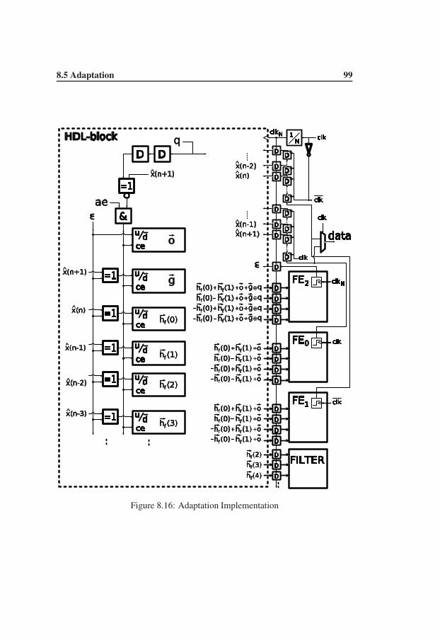
8.5 Adaptation 99
Figure 8.16: Adaptation Implementation

100 Implemented Equalizers
multiplexer controlled by the clock to form the DDR output data stream. Thesignals are also connected to series to parallel converters. The comparator in theupper FE block is clocked by a clock signal that is synchronous with the otherclock signals but has a frequency of 1/N times the normal clock frequency. Thissignal also clocks the adaptation logic of the HDL-block in figure 8.16.
The HDL-block has, in contrast to the other parts of the DFE, been gener-ated from a hardware description language-code (HDL-code). The HDL-blockincludes the coefficient counters to store and update the filter coefficients andadders to generate individual look-ahead values for the hf (0) and hf (1) filter tapsimplemented in the FE-blocks. The block also include different control functions,a serial interface through which counter lengths (µ) and counter values can be readand set. The block also has functionality to halt the adaptation, estimate the eyehight and handle selective adaptation when repetitive data patterns are received.
The adaptation is performed in the following way: A PRBS-generator givesa single bit q which corresponds to the guessed value of x(n + 1). Dependingon the value of q, ~g will either be added to or subtracted from the look-aheadcoefficients of the upper FE block. On the rising edge of the clkN clock signal,those values, the look-ahead values for the other FE blocks, and the filters areloaded into a set of registers and used as the DFE filter coefficient of the receiver.The comparator in the uppermost FE block will sample the input value at thefalling edge of the clkN . The comparator in the middle FE block will at the sametime sample the data that corresponds to x(n + 1). The number of D-flip-flops inthe serial to parallel converter is chosen so that the value will be clocked into aregister sending data to the HDL-block at the rising edge of the clkN signal. Asillustrated in figure 8.16, the potential error signal ǫ and a vector that correspondsto x(n+1), x(n), x(n−1) etc are also sent to the HDL-block at the rising edge ofthe clkN clock. The value of x(n + 1) is compared to the corresponding guessedvalue of q and if they are identical (and if adaptation is enabled by a high aesignal), the coefficient holding counters will count either up or down.
8.5.5 Individual Offset Estimation
As DACs and comparators are implemented individually for each FE block, theoffset between them can differ. As it is ǫ that will be minimized in the adaptationalgorithm, it will be the offset in the ǫ extracting FE block that will be compen-sated for in the adaptation. To extract the offset of the other FE blocks, they haveto perform the extraction of ǫ. As adaptation does not need to be performed con-tinuously there is the possibility to run several FE blocks in parallel and therebychange the role of the blocks without loosing data. To enable that functionality, anumber of switches where added in the first test chip. The switches and the FEblocks are shown in figure 8.17. The switches were controlled by a state machine

8.5 Adaptation 101
in the HDL-block. The figure shows the switch settings when the FE0 block re-ceives data at the negative edge of the clock, FE1 receives data at the positiveedge of the clock, and FE2 receives ǫ.
The role changing function is illustrated by the following example: To changefrom the state in figure 8.17 to the state where FE1 extracts ǫ and FE2 receivesdata at the positive clock edge, the state machine will control the switches asfollows. First stop the coefficient adaptation by pulling ae in figure 8.16 lowand change the settings of switches 8, 9, 10, and 11 so that they are identical toswitches 4, 5, 6, and 7. The FE1 and FE2 blocks will then run in parallel withidentical input data and therefore identical output data. Second, change switch 13and 1 to their lower positions so that FE2 will be the block used to receive data.Third, change switch 12 to the middle position, switch 4 to the lower position,switch 5 to the middle position, switch 6 to the upper position and switch 7 to theupper position. Block FE1 will then be configured to receive ǫ.
The HDL-block is then configured to add the ±g value to FE1 instead of FE2
and a separate offset counter is used during adaptation to estimate the offset ofFE1 instead of FE2.
8.5.6 Handling Data Pattern Correlation
The adaptation does not behave well if the vector ~x is the same all the time. Theadaptation will only have the option to “walk” in a direction that will not end upin the minimum as discussed in section 6.4 in chapter 6. The adaptation algorithmoperates at a pace that is 2·N times lower than the data rate7. If the data pattern hasa periodicity of 2N the adaptation will always see the same vector ~x. To minimizethat risk, the value of N is programmable between 20 and 21. The division factoris selected by a PRBS-generator in the HDL-block.
This strategy will only work if there is activity on the bus. Regardless of N ,there will only be one direction to walk if the bus is fixed low or high. To handlethis, the number of ones is counted in the ~x-vector. If the number is higher thana programmable threshold or lower than another programmable threshold, the aesignal in figure 8.16 will be pulled low and the adaption will stop.
References
[1] T. G. Noll, “Carry-Save Architectures for High-Speed Digital Signal Process-ing,” Journal of VLSI Signal Processing, pp. 121–140, 1991.
7The clock is divided by N and two bits are received every clock cycle.

102 Implemented Equalizers
Figure 8.17: Switches to swap FE block tasks

Chapter 9
On-chip Diagnostics
To be able to evaluate and compare different high-speed signaling implementa-tions, performance measures are needed. The two most commonly used perfor-mance measures are the eye diagram and the bit error rate (BER).
The eye diagram is as described in chapter 4, a graphical way of showing therobustness of the communication channel for time and amplitude disturbances.For the case when an open eye can not be guaranteed, the statistical measure biterror rate (BER) can be used.
The BER measures the probability of a transmitted bit being misinterpretedat the receiver. The BER measure is frequently used in radio communicationand fiber optics communication, but with increasing data rates for wire line com-munication and therefore smaller robustness margins, the measure has also beenadopted for short-range electrical wire communication channels.
For multi-Gb/s communication, the task of measuring the performance of acommunication channel is far from trivial. The whole idea is to develop state ofthe art electrical communication. Having the same data-rates from a test chip toany measuring equipment will be just as critical as the communication channel wewant to evaluate. To eliminate this communication problem, on-chip evaluationblocks have been used in the test chips.
9.1 Bit Error Rate Measurements
Measuring BER is theoretically quite simple. Transmit a number of symbols overthe channel, compare the received symbols with the transmitted ones, count thedifferences and the BER is the ratio BER = number of errors
total number of symbols .An implementation that has built in BER measurement capability is presented
in for instance [1]. Here Sohn et. al. generates a pseudo random binary sequence(PRBS) at the transmitter, send it over the channel and compare the received signal
103

104 On-chip Diagnostics
Figure 9.1: BER measuring blocks
with an identical sequence.
The test chips that have been designed include circuitry for BER estimation.The circuit implementation for BER measurements is shown in figure 9.1.
Here we have two PRBS generators, which basically are shift registers withfeedback. The two PRBS generators are 21 and 23 bits long, which gives se-quences that repeat after 221 − 1 = 2097151 and 223 − 1 = 8388607 bits respec-tively. The two sequences are multiplexed together to one stream to generate aDDR data stream. This signal is passed through a buffer and is transmitted offchip. The signal travels through the PCB channel to a receiver chip and the de-cision feedback equalizer (DFE), described in chapter 8. The two data streamsfrom the two data receiving comparators are sent to two serial to parallel con-verters. These high-speed data streams are converted from a serial stream to adigital word (32 bits wide in our implementation) and sent to a block generatedfrom HDL code. Here the data word is compared to a word generated by identicalPRBS generator blocks in the receiver test chip. The number of discrepancies aresummed and accumulated in an error register, which can be read through a serialinterface.
By calculating the number of bits sent without any change in the error register,the BER can be estimated.
The PRBS generators in the transmitter and receiver chips can also be con-figured to generate a repetitive pattern. The pattern in each PRBS generator isprogrammable and the length of the pattern has been set to 20 bits. The mul-tiplexed transmitter signal can therefore be programmed to be any 40 bits longpattern.

9.2 Eye Opening Extraction 105
Figure 9.2: Extra hardware added for eye opening extraction
9.2 Eye Opening Extraction
For communication with no or very few errors, the BER values give only limitedinformation. It will verify that the communication works but not how robust thecommunication is for various kinds of interference. For that case an eye diagramgives better information. The parasitic load of even the state of the art measure-ment equipment is substantially larger than the one from an on-chip transistorstage. Therefore, using on-chip circuitry to measure an eye diagram will give po-tentially more accurate measurement results by not disturbing the circuitry. In [2],Martin et. al. present an 8 Gb/s simultaneous bidirectional point-to-point linkwith an on-chip diagnostic circuit, which can be used to extract an eye diagram.
For a receiver with an equalizer, the problem of extracting an eye diagram willbe even more problematic. As the equalizer is used to mitigate the eye closingISI, the pre-equalizer off chip eye does not give information about the robustnessof the communication channel. That information can only be extracted from theeye diagram after equalization. That signal is normally only available on-chip. Tobring the equalized signal off chip would add huge parasitics which would ruinthe performance of the equalizer.
In [3] Sorna et. al. describes how to measure an internal eye opening, as weunderstand by sweeping an internal offset. The way we use to extract an internaleye diagram is fairly similar.
In section 8.5 we describe how to add blind adaptive coefficient extraction byadding a third DAC to estimate the sign of the error. As our channel characteris-tics change very little over time, we do not have to run the coefficient adaptationall the time. By adding a small peace of logic (from a HDL description) andutilizing the hardware normally used for coefficient adaptation, we can add theability to extract the eye diagram after equalization. The extra hardware neededis shown in figure 9.2. The extra hardware consists of two counters (10 bits eachin the implemented test chips), which can be read and reset through a serial inter-face, the Top/Bottom signal which is controlled via the serial interface and a fewlogic gates. The algorithm to extract the height of an eye diagram with this extrahardware is as follows:

106 On-chip Diagnostics
1. Set the Top/Bottom switch to send out a zero.
2. Set the maximum offset to the comparator which extracts ǫ.
3. Reset both counters and wait a short period of time. During this time the“All counter” will count up for every received data which is the same as theoutput of the Top/Bottom switch. The “Fractional counter” will count upfor each data that is the same as the output of the Top/Bottom switch andfor which the sign error signal (ǫ) is one. Both counter will stop when the“All counter” reach its maximum value.
4. Read the value from both counters.
5. Decrease the offset of the third comparator if possible and repeat the se-quence from item number 3.
6. If the minimum offset is reached and the Top/Bottom switch sends out azero, set the Top/Bottom switch to send out a one and repeat the sequencefrom item number 2.
The sequence above will generates two vectors of numbers between 0 and1023 from read-out of the “Fractional counter” values. Examples of such vectorsare shown in figure 9.3 Here the line labeled “one” denotes the ratio of receivedones when the received data was one. As shown, the fraction of ones starts todecrease for an offset of around 4. This indicates the lower limit of the top lineof the eye. In the same manner, the line labeled “zero” in figure 9.3 decreases tozero at an offset of around −15. This indicates the upper limit of the lower line inthe eye diagram. The estimated eye opening is thus between the upper and lowerline as indicated in the figure. To extract more information from the diagram wecan see the slope of the curves as the intensity of the line for the following reason:Consider one of the lines in figure 9.3 at two adjacent offset values. A smallervalue at the upper offset value shows that a smaller number of ones have beenreceived compared to the lower offset. A number of signals have disappeared.The difference represents the number of signals that have passed between theseoffset values.
To extract the width of the eye, we need to change the sample time of the ǫ-extracting comparator in fractions of the symbol time. For the test chip evaluationthis has been performed by changing the variable delay between the transmitterclock and the receiver clock (see figure 9.1). The delay were changed in smallsteps and vectors corresponding to the ones in figure 9.3 were extracted for eachstep. From this information we can generate an eye diagram as the one in fig-ure 9.4. The dotted line in figure 9.4 shows the line of the eye diagram that hasbeen generated from the information in figure 9.3.

9.2 Eye Opening Extraction 107
−30 −20 −10 0 10 20 300
200
400
600
800
1000
1200270
° phase shift
Fra
c. counte
r num
ber
Sign−error comparator offset (DAC value)
zero
one
open eye area
Figure 9.3: Internal eye opening result for one phase
Figure 9.4: Extracted eye opening example

108 On-chip Diagnostics
References
[1] Y.-S. Sohn, S.-J. Bae, H.-J. Park, and S.-I. Cho, “A Decision Feedback Equal-izing Receiver for the SSTL SDRAM Interface with Clock-Data Skew Com-pensation,” IEICE TRANSACTIONS on Electronics, vol. E87-C, pp. 809–817,May 2004.
[2] A. Martin, B. Casper, J. Kennedy, J. Jaussi, and R. Mooney, “8Gb/s Differ-ential Simultaneous Bidirectional Link with 4mV 9ps Waveform Capture Di-agnostic Capability,” in IEEE International Solid-State Circuits Conference,
Digest of Technical Papers, vol. 1, pp. 478–479, 2003.
[3] M. Sorna, T. Beukema, K. Selander, S. Zier, B. Ji, P. Murfet, J. Mason,W. Rhee, H. Ainspan, and B. Parker, “A 6.4Gb/s CMOS SerDes Core withFeedforward and Decision-Feedback Equalization,” in IEEE International
Solid-State Circuits Conference, Digest of Technical Papers, vol. 1, pp. 62–63,February 2005.

Chapter 10
Test Chips
As the alert reader has certainly noticed by now, two test chips have been designedin the project that has resulted in this thesis. This chapter describes the test chips,and evaluation of them.
10.1 Chip 1
The first test chip was developed during the spring and summer of 2004. The pro-cess used was ST microelectronics, 0.18 µm CMOS. A photo of the implementedchip is shown in figure 10.1.
10.1.1 Implemented Features
The test chip included the following parts:
• Decision feedback equalizer with 16 filter taps and 6 bit arithmetic.
• Blind adaptation logic, eye diagram extraction logic, serial interface for con-trolling and configuring the equalizer.
• Data activity handling logic and comparator offset control logic.
• PRBS and repetitive pattern generators for off-chip data drivers.
• PRBS and repetitive pattern generators for off-chip crosstalk generation.
• Transmission error counting logic with programmable propagation delaycompensation.
109

110 Test Chips
Figure 10.1: test chip 1 micro-graph

10.2 Measurement Results of Chip 1 111
The DFE has the structure shown in figure 8.1 in chapter 8. The input stageis similar to the one shown in figure 8.2 except that there are no cascode tran-sistors1. The resistor values were chosen so that the input impedance was 190 Ωfor nominal temperature and typical process corner. The comparator is identicalto the one shown in figure 8.3. The filter taps that the digital filter consists ofare shown in figure 8.7. The blind adaptation were implemented as in figure 8.16with programmable 24 bits long coefficient counters. The DFE implementationincludes the switches shown in figure 8.17 and the adaptation block includes astate machine to automatically control the switches to change comparator task.
The implemented chip evaluation circuitry has the structure shown in fig-ure 9.1. The PRBS registers used to generate transmitted data are 21 and 23 bitslong. Both can be configured to generate 20 bits long repetitive patterns. The testchip includes two more pattern generators and off chip driver circuits. They areused to generate activity on adjacent lines, emulating crosstalk. The shift registerlengths of these are 17 and 19 bits and 20 and 21 bits respectively.
The error counting logic compares two data streams from the two data gener-ating PRBS registers and the positive edge and negative edge data from the DFEseparately. The number of errors in each comparison is accumulated in a 24 bitregister. The data streams can be compared at a programmable delay offset of 0to 15 bits.
The chip area was (including PADs) 2.1 mm x 2.1 mm. The area of theequalizer was 0.14 mm2. The adaptation, control, and interface block occupied0.65 mm2 and the area of the pattern generator, driver, and error counting blockwas 0.36 mm2.
10.2 Measurement Results of Chip 1
10.2.1 Filter Timing
The circuit was first tested using a high quality point to point channel. Data wasnot received correctly for data-rates over 800 Mb/s neither for zero nor for non-zero DFE filter coefficients. When the bias current to the DACs was shut of, PRBSdata was received correctly up to 1.8 Gb/s (BER < 5 · 10−12) which was close tothe simulated performance of 2 Gb/s.
The carry-save data representation in combination with the high fan-out of thecomparator nodes were found to be the cause of this behavior. With all coefficientsset to zero, the filter output should be a constant zero value. With the redundantdata representation used, the value zero can be represented in more than one way.
1The transistors having the gate connected to the node b in figure 8.2.

112 Test Chips
Therefore, the zero data filter output was filter input data dependent. Underesti-mation of the parasitics of the comparator high fan-out node caused late arrival ofthe filter input signal and therefore errors in the filter output data.
Due to this timing problem, the equalizer circuitry had to be evaluated at data-rates below 800 Mb/s. With a margin to the timing error issues, 700 Mb/s wasused as the data rate during evaluation.
10.2.2 Memory Bus Evaluation
The aim of the test chip was to illustrate high data-rates over a multi-drop bus thatresembles a DRAM DIMM bus. For that purpose a PCB board with four DIMMconnectors was designed. From these a 10 cm single ended data path was usedto connect the DFE receiver of a test chip. PCBs emulating single rank DRAMDIMMs were also designed. The boards could be used in two ways, either witha test chip bonded to generate data and crosstalk emulating signals, or as a non-sending passive board with surface mounted termination resistors and capacitors.With this setup no more than one equalization tap was needed to retrieve the data.The test chip had a 16 tap filter.
The signal speed in transmission lines is roughly constant. As bit-rates in-crease, fixed reflection delay will cause ISI to spread over more bits. To test thecapability of the long filter structure, an extra 45 cm long unterminated stub wasused. When transmitting at 700 Mb/s, this channel corresponds to a realistic multi-drop memory channel at around 5 Gb/s with respect to reflection caused ISI. Thetest setup used in the following evaluation is shown in figure 10.2.
10.2.3 Eye Opening
The ISI injected when transmitting at 700 Mb/s will completely close the eye in aneye diagram. This is shown in figure 10.3(a). This signal was fed to the equalizerin the test chip. The blind adaptive algorithm of the equalizer set the equalizercoefficients. The resulting eye opening at the input of the internal comparator isshown in figure 10.3(b). This figure was generated according to the algorithmdescribed in section 9.2 in chapter 9. The dotted lines in figure 10.3(b) representthe phase where the coefficient updating algorithm was run, i.e. this was the phasewhere the circuit tried to open an eye. By changing the clock phase betweentransmitter and receiver we show that an eye could be opened at more than onephase. Figure 10.4 shows the eye opening for 4 different phases. Here one bit-time represents 180. Figure 10.4 shows that we could open an eye over 130,meaning 72% of the whole bit-time. The error bit counter did not count any errorsat any of these phases (BER < 1 · 10−11), showing that the indirectly measuredeyes shown in figure 10.3(b) and 10.4 correspond to real open eyes.

10.2 Measurement Results of Chip 1 113
Figure 10.2: Measurement setup, test chip 1
10.2.4 Channel Estimation
From the filter coefficients in the equalizer, we can estimate the characteristics ofthe channel. From equation (5.16) in chapter 5 we see that the optimum filter co-efficients are identical to post-cursor of the impulse response of the channel. Therecovered signal in equation (5.17) is scaled with the first coefficient of the chan-nel impulse response. That value is the same as half of the equalized eye openingand from section 8.5.2 in chapter 8 we see that this value is set by the adaptationparameter g. Equation (10.1) then shows how to estimate the impulse response(hc) of the channel from the filter coefficients. The step response of the channelis then given according to equation (10.2). Using equalizer parameters from dif-ferent phases, we can estimate the step response with higher time resolution. Theparameters used in the equalizer filter when creating figure 10.3(b) and 10.4 re-sult in a step response of the channel shown in figure 10.5(b). The correspondingstep-response, measured using an external oscilloscope is shown in figure 10.5(a).
hc(n) =
g n = 1hf(n − 1) n > 1
(10.1)

114 Test Chips
(a) Eye opening at the receiver
(b) Internal eye opening
Figure 10.3: Eye openings, at 700Mb/s

10.2 Measurement Results of Chip 1 115
(a) 9.9 (b) 40.5
(c) 120.6 (d) 140.4
Figure 10.4: Eye openings at different phase shifts

116 Test Chips
Block Current [mA])Receiver equalizer, clock generation, pattern generation, andBER counters
61
Adaptation logic 2IO 4DIMM board transmitter 6DIMM board pattern generator 38
Table 10.1: Current consumption break down for test chip 1 at 700 Mb/s
sc(n) =n∑
m=0
hc(m) (10.2)
10.2.5 Power Consumption
The current consumption of the different parts of test chip 1 shown in table 10.1.The values are given for measurements at 700 Mb/s and the supply voltage usedwas 1.8 V. The power supply of several blocks were connected together due tolimited number of PADs. The fist line of table 10.1, (receiver equalizer etc.) andthe last line (DIMM board pattern generator) gives the current for the same supplypad but at the receiver bonded chip and the transmitter chip respectively. Thedifference between the values are due to the lack of activity in the equalizer forthe DIMM board. The difference indicate the dynamic current consumption of theequalizer2.
10.2.6 Adaptation and Individual Offset Estimation
The individual offset estimation logic described in section 8.5.5 in chapter 8,was implemented on the chip. The functionality worked well together with theother blind adaptation. For all blind adaptation, measurements showed a tendencyfor errors rates with the adaptation running compared to when it was stopped.The tendency was stronger the shorter updating counter used (larger values for µ)which is consistent with the discussion in section 6.3 in chapter 6.
The convergence of the adaptation was found to be, as expected, dependent onthe initial value. With a large positive initial g and µg
3 being two to four times the
2Note that the current of the clock generating blocks are included in both values and that theactivity of these block are identical for both the receiver and DIMM chips.
3From equation (8.11).

10.2 Measurement Results of Chip 1 117
(a) Step response measured off-chip at the receiver
0 2 4 6 8 10 12 14 16 18 200
5
10
15
20
25
30
35
40
45Extracted step−response
Time (ns)
DA
C v
alu
e
9.9o
40.5o
80.1o
120.6o
140.4o
(b) Step response, extracted from equalizer coefficients
Figure 10.5: Channel step response, determined in two different ways

118 Test Chips
values for µf4, the adaptation showed robust convergence even for channels with
ISI completely closing the eye diagram.
10.2.7 Crosstalk
The test chip and the PCB had the possibility to drive signals on two wires going inparallel to the signal wire at a distance of three times the signal wire. These wireswere used to emulate crosstalk. Figure 10.6 show measured eye diagrams at thereceiver test chip with and without crosstalk signals. The board configuration usedhere is the configuration marked B3 in figure 10.10 but for the test chip one board.As shown, crosstalk does severely influence the eye opening. The eye diagramafter the on-chip equalization were also extracted for the signals in figure 10.6.These are shown in figure 10.7. The difference between the internal eyes is notlarge. For this example, removing the ISI through equalization improves signalintegrity more significantly than elimination of crosstalk.
10.3 Chip 2
As a result of the unsatisfying performance of the DFE filter of the first test chip,a second test chip was designed. This chip was designed during the spring andsummer of 2006. As the 0.18 µm process used for the first test chip was no longeravailable to us, the second test chip was designed in ST-microelectronics, 0.13 µmCMOS technology. A photo of the implemented chip is shown in figure 10.8. Thechip area was (including PADs) 1 mm x 1 mm. The equalizer circuit occupies0.047 mm2 and the coefficient updating logic 0.14 mm2.
10.3.1 Implemented Features
The test chip includes the following parts:
• Decision feedback equalizer with 12 filter taps and 8 bit arithmetic.
• Blind adaptation logic, eye diagram extraction logic, serial interface for con-trolling and configuring the equalizer.
• Data activity handling logic.
• PRBS and repetitive pattern generators for off-chip data drivers.
• PRBS and repetitive pattern generators for off-chip crosstalk generation.
4From equation (8.12).
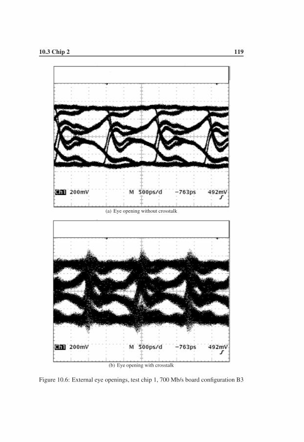
10.3 Chip 2 119
(a) Eye opening without crosstalk
(b) Eye opening with crosstalk
Figure 10.6: External eye openings, test chip 1, 700 Mb/s board configuration B3

120 Test Chips
(a) Interal eye opening without crosstalk
(b) Internal eye opening with crosstalk
Figure 10.7: External eye openings, test chip 1, 700 Mb/s board configuration B3

10.4 Measurement Results of Chip 2 121
Figure 10.8: Test chip 2 micro-graph
• Transmission error counting logic with programmable propagation delaycompensation.
The overall DFE structure of the second test chip was identical to the first testchip (figure 8.1 in chapter 8). The input stage is shown in figure 8.2. The resistorvalues were identical to the first test chip and the input impedance was thereforeagain 190 Ω. The comparator structure was not changed (figure 8.3). The im-plemented filter is described in section 8.4.7. The individual offset estimationfunctionality described in section 8.5.5 was not implemented to improve the oper-ating speed. Blind adaptation similar to the one in figure 8.16 with programmable32 bit long coefficient counters was implemented.
The pattern generator, driver circuits, and error counting block were identicalto the blocks used in test chip 1.
10.4 Measurement Results of Chip 2
10.4.1 Adaptation
Removal of the individual offset estimation enabled simplification of the clockdistribution as programmable clocking was no longer needed. The error extraction

122 Test Chips
comparator (see figure 8.16) was clocked with the high frequency clock instead ofthe divided clock signal. The result was that the error extraction comparator hadan evaluation time of less than one high frequency clock phase time compared toone clock phase of the divided clock signal for the first test chip. The differenceis a factor of ten and as the error extraction comparator has a higher exposure tometastability (see section 8.5.4) the result was significantly lower performance forhigh data-rates.
Initial measurements showed poor performance when receiving PRBS data.The problem was eventually located to the error extraction comparator block. Theclocking of that block interfered with the other comparator blocks resulting intransmission errors. The errors were data pattern dependent. The transmitter pat-tern generator block was designed to generate a 20 clock cycle long pattern. Thefunctionality to configure the DFE clock divider between N = 20 and N = 21(see section 8.5.6) enabled the functionality to move the error extraction com-parator evaluation time to a phase in the repetitive pattern where the effect of thedisturbances was minimized. The drawback was that there were no ways to avoidthe condition with a “fixed walking” direction (see section 8.5.6). The blind adap-tation logic could therefore not be used, the eye height functionality described insection 9.2 did not work, and evaluation was limited to a repetitive data pattern.
10.4.2 Equalizer
After identifying the adaptation problem, the implemented DFE performed well.The chip was tested with bit-rates up to 2.8 Gb/s and was able to receive a non-trivial pattern at this rate. The value corresponds well to the simulated maximumdata-rate of the FIR filter which was just above 3 Gb/s for extracted layout. Toadd a little bit of margin, bit-rate evaluations were made at 2.6 Gb/s.
10.4.3 Multi-drop Bus
An evaluation board for a four drop memory bus was also developed for the sec-ond test chip. The board is shown in figure 10.9. The board was tested using thesame memory board configurations as the modeled channel in section 3.3 in chap-ter 3. To illustrate the ISI conditions of the board, figure 10.10 shows eye openingmeasurements at the receiver chip, using a 4 GHz probe, at 2.6 Gb/s for the threedifferent module configurations.
As the eye opening extraction functionality did not work, only the bit error ratewas available as a measure of the performance of the equalizer. Figure 10.11(a)shows BER vs sampling phase for the three receiver setups in figure 10.10. Datawas received at 2.6 Gb/s and the equalizer coefficients used in the DFE are shown

10.4 Measurement Results of Chip 2 123
Figure 10.9: Measurement setup, test chip 2
in figure 10.11(b). The equalizer coefficients was set manually for these measure-ments as the blind adaptation caused transmission errors. As shown, the equalizerwas able to recover the data with a BER < 10−9 at > 20% of the symbol timewith one set of filter coefficients per measurement setup.
10.4.4 Power Consumption
The current consumption of the different parts of test chip 2 shown in table 10.2.The values are given for measurements at 2.6 Gb/s and the supply voltage usedwas 1.2 V. As shown, the majority of the current consumption relates to the highspeed digital blocks. The design was optimized for performance and the currentconsumption was barely addressed during the design process. As a large portionof the current consumption is related to digital logic, further optimization andnewer technology generations have the potential to substantially reduce the currentconsumption of the used equalizer structure.

124 Test Chips
Figure 10.10: Eye diagram before equalization for three different module config-urations
10.5 Test Chip Summary
There were a number of goals with the design of the test chips. The goals andwhether they were met are summarized in table 10.3. The structures of the twotest chips were very similar, still the results that were possible to extract from thechips were quite different. The first chip showed the performance of the adapta-tion and the on-chip evaluation circuitry as well as the individual offset estimation.The second test chip showed the equalization performance of the used DFE struc-ture and how it could be used for memory buses with many endpoints. Still, thecombination of the two gave satisfying results.
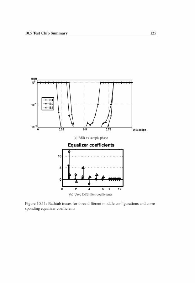
10.5 Test Chip Summary 125
(a) BER vs sample phase
(b) Used DFE filter coefficients
Figure 10.11: Bathtub traces for three different module configurations and corre-sponding equalizer coefficients

126 Test Chips
Block Current [mA])All digital parts of the equalizer including FIR filter includinghf(0) and hf(1) look ahead and adaptation logic
48
On-chip clock generation circuits 30BER evaluation circuits 18Comparators and DACs 14Input stage (vc) 2IO 8DIMM board transmitter 16DIMM board pattern generator 8
Table 10.2: Current consumption break down for test chip 2 at 2.6 Gb/s and boardconfiguration B3
Fulfilled withGoal Chip 1 Chip2Show multi-Gb/s transmission over a memory bus with alarge number of endpoints
No Yes
Equalization of a bus with extensive ISI Yes YesBlind adaptation to autonomously retrieve effective equalizercoefficients.
Yes No
Characterization of the channel characteristic through blindadaptation
Yes No
Autonomous offset estimation Yes NoOffset compensation Yes YesEqualized eye-opening extraction Yes NoBit error rate estimation through on-chip pattern generatorsand error counters
Yes Yes
Table 10.3: Test chip evaluation goals

Chapter 11
Reciprocal Bidirectional
Equalization
The idea of using the reciprocal properties of a passive linear channel to performchannel equalization only on the host side of a multi-drop memory bus was pre-sented in section 3.4 in chapter 3. The idea is to use a blind DFE to equalizereceived data at the memory host controller and reuse the retrieved channel infor-mation for a linear transmitter equalizer. The characteristics of the channel can beextracted from the DFE filter settings (see section 5.3) and the DFE filter settingscan be set by blind adaptation (see section 6.3). If the reciprocity theorem can beapplied to the system, the extracted channel characteristics can be used in the lin-ear transmitter equalizer. This chapter presents simulations to show that the ideaholds also for transistor based driver circuits.
11.1 Channel Characteristics
The channel model used in section 3.3 was made for the Hspice simulator. Themodels that have been available to us for accurate transistor simulations are for theSpectre simulator. For simulation of a multi-drop channel and accurate transistormodels, a channel model for the Spectre simulator was created.
The channel model is a four-drop bus, shown in figure 11.1. The channel hasbeen modeled using capacitors and inductors (to model pad capacitance and bondwire inductance), ideal transmission lines (modeling PCB strip lines), and termi-nation resistors. The values have been chosen so that the step response betweenthe host (marked H in the figure) and each of the four memory modules (markedM1-4 in the figure) resembles the step response generated from the Hspice modelin section 3.3.
127

128 Reciprocal Bidirectional Equalization
Figure 11.1: Channel model
11.2 Reciprocity
In order for the reciprocity theorem to apply, the termination impedance has tobe constant at all times (see section 3.4). Transistors acting as current mirrorswill have high output impedance and can easily be switched off. The receiverimpedance is for this case set by the termination resistors in parallel with thecurrent mirrors’ output impedance. If the endpoints are terminated with resistorsthat are low compared to the output impedance of the current mirrors, then thetotal receiver impedance stays fixed even if the impedances of the current mirrorsvary with signal voltage.
Transistors driving off-chip signals tend to be large. Large transistors havelarge parasitic capacitances. Capacitances have low impedance at high frequen-cies. Still, this is not a problem as long as the capacitances are fixed and inde-pendent of the signal voltage. Any fixed capacitance can be seen as part of thepassive linear channel and will therefore not remove the reciprocal properties ofthe channel.
11.3 Equalization Circuitry
To demonstrate that reciprocity can be utilized in practice, the designed DFE intest chip 2 has been modified to include an additional linear transmit equalizer.
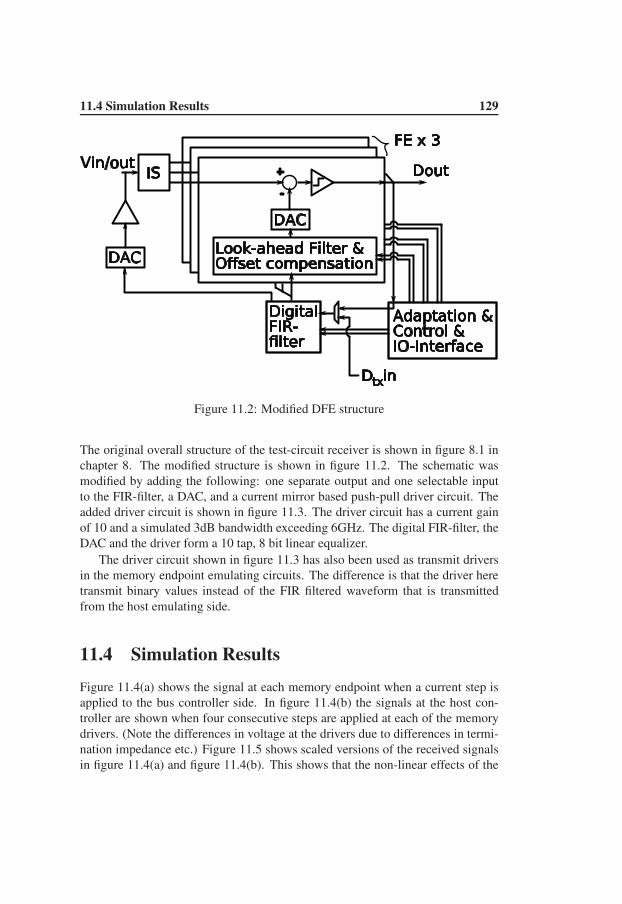
11.4 Simulation Results 129
Figure 11.2: Modified DFE structure
The original overall structure of the test-circuit receiver is shown in figure 8.1 inchapter 8. The modified structure is shown in figure 11.2. The schematic wasmodified by adding the following: one separate output and one selectable inputto the FIR-filter, a DAC, and a current mirror based push-pull driver circuit. Theadded driver circuit is shown in figure 11.3. The driver circuit has a current gainof 10 and a simulated 3dB bandwidth exceeding 6GHz. The digital FIR-filter, theDAC and the driver form a 10 tap, 8 bit linear equalizer.
The driver circuit shown in figure 11.3 has also been used as transmit driversin the memory endpoint emulating circuits. The difference is that the driver heretransmit binary values instead of the FIR filtered waveform that is transmittedfrom the host emulating side.
11.4 Simulation Results
Figure 11.4(a) shows the signal at each memory endpoint when a current step isapplied to the bus controller side. In figure 11.4(b) the signals at the host con-troller are shown when four consecutive steps are applied at each of the memorydrivers. (Note the differences in voltage at the drivers due to differences in termi-nation impedance etc.) Figure 11.5 shows scaled versions of the received signalsin figure 11.4(a) and figure 11.4(b). This shows that the non-linear effects of the

130 Reciprocal Bidirectional Equalization
Figure 11.3: Bus driver circuit
driver and receiver circuits do not remove reciprocity of the channels and that thechannel characteristics acquired from the blind receiver equalizer therefore arevalid also for a linear transmitter equalizer.
Based on the channel characteristics, Wiener filter theory (see section 5.2)was used to calculate filter coefficients for the linear transmitter equalizer. As thechannel characteristics are different for each of the memory units, four sets of ten8-bit coefficients was calculated, one for each memory block.
Figure 11.6 shows the simulated eye openings at the memory blocks when thecorresponding coefficient sets have been used. The coefficients used are shownin figure 11.7(a). As a comparison, figure 11.7(b) shows the eye opening at M4when the transmitter equalizer is using the coefficients for M1. All eye openingdiagrams have been generated by transmitting PRBS data at 3 Gb/s.
11.4.1 Latency
As a DFE uses the received data in the time critical feedback loop, the data la-tency of this equalizer structure is inherently low. For linear transmitter equalizerspipelining is often used and the data latency in the filter also depends on the filtercoefficients. For a channel with small precursor in the impulse response (e.g. thechannels used here) efficient linear filter coefficients can be found that keep thesignal latency low. As the DFE filter has to be optimized for low latency, we canbenefit from this design constraint when reusing it for a linear transmitter equal-izer. As for the implementation presented here, the shortest path from data inputto analog output (see figure 11.2) contains only one dual-edge flip-flop. As a re-sult, the latency in the simulation results shown in figure 11.6 and figure 11.7(b)have a transmitter latency of only one bit time.

11.4 Simulation Results 131
0 1 2 3 40
0.5
1
Time [ns]
Voltage [V
]
Step responses from host to memories
HM1M2M3M4
(a) Host to memories
0 1 2 3 40
0.5
1
Time [ns]
Receiv
ed v
oltage [V
]
Step responses from memories to host
M1M2M3M4H from M1H from M2H from M3H from M4
(b) Memories to host
Figure 11.4: Step responses

132 Reciprocal Bidirectional Equalization
0 0.5 1 1.5 2 2.5 3 3.5 40
0.2
0.4
0.6
0.8
1
1.2
Time [ns]
Re
ce
ive
d v
olta
ge
[V
]
Step responses in both directions
M1−>H
M2−>HM3−>H
M4−>HH−>M1
H−>M2H−>M3
H−>M4
Figure 11.5: Scaled step responses in both directions

11.4 Simulation Results 133
0 0.1 0.2 0.3 0.40.45
0.5
0.55
0.6
0.65
0.7
0.75
Time [ns]
Voltage [V
]
Eye opening at node M1
(a) H to M1
0 0.1 0.2 0.3 0.40.45
0.5
0.55
0.6
0.65
0.7
0.75
Time [ns]
Voltage [V
]
Eye opening at node M2
(b) H to M2
0 0.1 0.2 0.3 0.40.2
0.4
0.6
0.8
1
Time [ns]
Voltage [V
]
Eye opening at node M3
(c) H to M3
0 0.1 0.2 0.3 0.40.2
0.4
0.6
0.8
1
Time [ns]
Voltage [V
]
Eye opening at node M4
(d) H to M4
Figure 11.6: Eye openings at different memory stubs

134 Reciprocal Bidirectional Equalization
0 2 4 6 8 10
−20
0
20
40
60
80
100
120
Coefficient [#]
Va
lue
Coefficients for the linear equalizer
To M1To M2To M3To M4
(a) Linear equalizer coefficients
0 0.1 0.2 0.3 0.4
0.4
0.5
0.6
0.7
0.8
0.9
1
Time [ns]
Vo
lta
ge
[V
]
Eye opening at node M4
(b) Host to M4 transmission when coefficients for M1 are usedin the equalizer
Figure 11.7: Equalizer coefficients and a bad eye example
Chapter 12
Conclusions and Future Work
12.1 Conclusions
Advances in technology and architectures are continuously increasing the dataprocessing capabilities of modern computers. The advances enable processingof increasing amounts of data at higher speeds. The progress therefore increasesthe demand for fast access to large amounts of memory, which in turn requirehigh data-rates, large maximum accessible memory, and low access latency forthe memory bus. These three requirements are hard to meet simultaneously and itwill be harder still when the requirement of low cost is included.
The dominating bus structure used for memory access is wide word lengthbuses with single ended signaling between one host and multiple end-user ex-pandable memory modules on a single bus. The trend has been to reduce thenumber of expansion slots on these types of buses to tackle signal integrity issuescaused by increased data-rates. Increased memory capacity per endpoint has notbeen able to fully compensate for this reduction which has resulted in a bus systemwith undesirable low maximum memory capacity.
The tremendous advance in semiconductor based data processing is the un-derlying mechanism that has driven the requirements of the memory bus. Thisthesis aims to show that this progress can be used to compensate for signal in-tegrity issues caused by high data-rate without reducing the number of endpointsand thereby suggesting a solution to the low maximum memory capacity prob-lem. The solution will show improved performance and reduced cost with futureprocess scaling. Furthermore, it will not add extra latency.
We first do this by estimating the maximum information transmitting capacityof a four endpoint bus based on a model. The result shows that there is a factorof ten to a hundred of unused potential compared to commercially used data ratesand that this factor is valid without any change to the bus structure.
135

136 Conclusions and Future Work
An equalizer structure has been developed which targets the extensive inter-symbol interference that appears on the addressed bus structure at multi-Gb/s sig-nal transmissions. The digital signal processing blocks of the structure enablesefficient endpoint switching which is advantageous for multi-drop buses. Usingthis structure, we have demonstrated data transmission at 2.6 Gb/s over a four-drop bus using a 0.13 µm CMOS test chip.
An efficient blind adaptation implementation has been developed that demon-strates the possibility to add equalization without the need for high level signalprotocols and that can compensate for slow channel variations during normal datatransmissions. Using blind adaptation to extract signal channel characteristics hasbeen demonstrated.
To minimize system cost and take full advantage of the memory bus controllerend-point signal processing capability, the use of single-sided equalization hasbeen proposed. The reciprocal properties of a channel and the channel charac-teristics extraction capability of a blind receiver equalizer enable us to suggestsingle sided equalization which eliminates the need for high level configurationreturn channels or startup protocols. We have illustrated single sided equalizationby reusing a DFE filter as a linear transmitter equalizer and we have used accu-rate transistor models for channel interface circuits to show that the reciprocityprinciple can be utilized in practice for these high speed buses.
Finally, do not be alarmed even if the eye diagram looks like a monster. Fur-ther improvements in date-rates are still possible by the use of signal processingrecovery circuitry.
12.2 Future Work
The work presented here has shown the potential of further improvements of themulti-drop memory bus. There are still a number of issues that need to be ad-dressed in order for the concept to function in a commercial application. Thereare also aspects of the presented equalizer strategy that have not been addressed.
From the theoretical capacity examples in chapter 3 we see that crosstalk isa major limit to the data capacity. A DFE subtracts the post-cursor of alreadyreceived data-bits. For a receiver at a parallel data bus, received data from adjacentlines are available to the receiver. Filtering these data in the same way as for aDFE will reduce the effect of crosstalk. A DFE can only compensate for post-cursor taps in the channel impulse response. A straight-forward implementationwould only be able to compensate for post-cursor crosstalk effects. The maincrosstalk term would be unaffected. With higher data-rates more and more energywill be in the post-cursor and not in the main tap. The compensation methodwould therefore be more effective as data-rates increase. Alternatively, look-ahead

12.2 Future Work 137
techniques could potentially be used to enable compensation also for the maincrosstalk tap.
Blind adaptation and single-sided equalization enable signal integrity and im-proved data-rates in a way that could be made transparent to higher level abstrac-tion protocols with one important exception. The used adaptation implementationrequires a large number of initial transmissions to set the filter coefficients cor-rectly. Data integrity can not be guaranteed during this startup phase. Transmit-ting data at a reduced rate during startup can ensure fault free data transmission.From an equalizer adaptation point of view, a reduced data-rate is equivalent withlow bus activity. An adaptation implementation that can guarantee good conver-gence for a bus with low activity could enable a system that are run at low bit-ratesduring startup and after equalization adaptation is complete at high bit-rates withadequate signal integrity. The only non-transparency of the transmissions willthen be configurable data-rates.
Synchronization between transmitter and receiver data is an issue that is crit-ical for reliable communication. The use of equalization does not remove thepossibility of reliable traditional synchronization methods, though blind adapta-tion offers a new approach to synchronization. The implemented adaptation logicpresented in this thesis estimates the height of the equalized eye as a part of theadaptation (parameter g in section 8.5.2). For a system with synchronous clocksources, it is only necessary to extract the correct phase of the received signal. Itis reasonable to assume that a maximum eye opening height corresponds to theoptimum phase. The signal g could be used to track that optimum phase.
Changing addressed endpoint and transmission direction efficiently is essen-tial to minimize unused bus transmission time. The equalizer implementationspresented here enable efficient switching between equalizer coefficient sets. Tochange each filter coefficient at the optimal time could enable changing addressedendpoint without waiting for all signal reflections to die-out on the bus. This hasthe potential to reduce the time for switching between endpoints to below thelength of the channel impulse response.

138 Conclusions and Future Work

Appendix
139


Appendix A
System Modeling
A.1 Linear Systems
Linear, time-invariant systems have a number of properties that makes them veryattractive as models. Superposition enables the whole transformation theory tool-box which enables us to analyze a system from a frequency point of view. A linearsystem is also the foundation for equalization techniques.
A system is linear if an input signal x to the system f generates the outputsignal y and satisfies equation (A.1) where a and b are arbitrary constants.
f (x) ⇒ y
f (a · x1 + b · x2) ⇒ a · y1 + b · y2 (A.1)
A subclass of linear systems is time-invariant linear systems. These systemshave constant characteristics over time which means that they obey equation (A.2)for any time, t and time delay, τ .
f (x (t)) ⇒ y (t)
f (x (t + τ)) ⇒ y (t + τ) (A.2)
The characteristics of a linear, time-invariant system can be fully described bythe system impulse response. The impulse response is the output signal h(t) wheninjecting a short pulse δ(t) at the input as in equation (A.3).
f (δ (t)) ⇒ h (t) (A.3)
Given an input signal x(t) the output signal y(t) can be calculated as the con-volution of the input signal and the impulse response according to equation (A.4).
y (t) = x(t) ∗ h(t)
=
∫ ∞
−∞
x (λ) · h (t − λ) dλ (A.4)
141

142 System Modeling
Figure A.1: Transmission line segment
The Fourier transform of the impulse response is a complex valued functioncalled frequency response H(ω) and describes how the system affects a signal asa function of frequency. For an input signal with frequency contents X(ω), theoutput signal will have a frequency content Y (ω) according to equation (A.5).
Y (ω) = X(ω) · H(ω) (A.5)
A.2 Transmission Line Equations
Consider a small segment (dx) of a line and the return path as in figure A.1. Us-ing Kirchhoff’s voltage and current laws to express the currents and voltages infigure A.1 will give equation (A.6) and (A.7).
v(x, t) − Rdxi(x, t) − Ldxdi(x, t)
dt− v(x + dx, t) = 0 (A.6)
i(x, t) − Gdxv(x + dx, t) − Cdxdv(x + dx, t)
dt− i(x + dx, t) = 0 (A.7)
Divide both equations by dx and let dx → 0 and we will find the so called Teleg-
rapher’s equations12 as in equation (A.8) and (A.9).
dv(x, t)
dx= −Ri(x, t) − L
di(x, t)
dt(A.8)
di(x, t)
dx= −Gi(x, t) − C
vi(x, t)
dt(A.9)
1The Telegrapher’s equations were here derived using circuit theory. The equations can alsobe derived directly from Maxwell’s equations [1].
2Some literature names another equation the Telegrapher’s equation. The definition of thereflection coefficient Γ is sometimes called the telegrapher’s equation [2] (See equation (A.31)where Z2 → ∞).

A.2 Transmission Line Equations 143
For the sinusoidal steady-state condition equation (A.8) and (A.9) can be writtenas in equation (A.10) and (A.11).
dV (x, t)
dx= −(R + jωL)I(x, t) (A.10)
dI(x, t)
dx= −(G + jωC)V (x, t) (A.11)
Isolating V and I in equation (A.10) and (A.11) result in the wave equations (A.12)and (A.13) with the complex propagation constant γ defined as in equation (A.14).
d2V (x, t)
dx2= −γ2V (x, t) (A.12)
d2I(x, t)
dx2= −γ2I(x, t) (A.13)
γ = α + jβ =√
(R + jωL)(G + jωC) (A.14)
Traveling wave solutions to equations (A.12) and (A.13) can be found as in equa-tion (A.15) and (A.16).
V (x) = V +0 e−γx + V −
0 eγx (A.15)
I(x) = I+0 e−γx + I−
0 eγx (A.16)
Applying equation (A.10) to equation (A.15) gives equation (A.17).
I(x) =γ
R + jωL
[
V +0 e−γx − V −
0 eγx]
= I+0 e−γx + I−
0 eγx (A.17)
From (A.17) we can identify the characteristic impedance for the forward andreverse wave as in equation (A.18).
Z0 =V +
0
I+0
=−V −
0
I−0
=R + jωL
γ=
√
R + jωL
G + jωC(A.18)
Equation (A.17) and (A.18) lets us write I(x) according to equation (A.19).
I(x) =V +
0
Z0e−γx − V −
0
Z0eγx (A.19)

144 System Modeling
The solution to the wave equation in equation (A.12) as shown in equation (A.15)can be written in time domain as in equation (A.20).
v(x, t) = |V +0 |cos(ωt− βx + Φ+)e−αx +
|V −0 |cos(ωt + βx + Φ−)eαx (A.20)
The phase velocity is the velocity for which one particular phase of the wave istraveling. One particular phase of the wave is characterized by that the argumentof the cos function is constant. Hereby the phase velocity (vp) can be derivedaccording to equation (A.21).
Constant = ωt − βx
x =Constant
β+
ωt
β
vp =dx
dt=
d(
Constantβ
+ ωtβ
)
dt=
ω
β(A.21)
The wavelength of the wave is defined according to equation (A.22).
λ =2π
β(A.22)
A.3 Loss-less Transmission line
PCB lines are often modeled as loss-less transmission lines. That means that theresistive and dielectric losses are neglectable. For a loss-less transmission lines thetransmission line parameters are reduced to the ones in equation (A.23) to (A.26).
R = 0 , G = 0 =⇒γ =
√−ω2LC = jω
√LC (A.23)
β = ω√
LC, α = 0 (A.24)
vp =1√LC
(A.25)
Z0 =
√
L
C(A.26)

A.4 Impedance Mismatch 145
Figure A.2: Transmission line mismatch
A.4 Impedance Mismatch
Consider a transmission line (T0) with impedance Z0 connected to another trans-mission line (T1) with characteristic impedance Z1 as illustrated in figure A.2.Consider a signal traveling through T0 towards T1. At the interface, a fraction Γof the signal will be reflected back into T0 according to equation (A.27) (see [2]or appendix A.5 where Z2 → ∞)
Γ =Z1 − Z0
Z1 + Z0(A.27)
As no signal is lost, what has not been reflected is transmitted into Z1 which thenis given by equation (A.28).
(1 − Γ) =2 · Z0
Z1 + Z0
(A.28)
A.5 Reflections in T-Connections
The topic of this thesis is communication over multi-drop buses. For multi-dropbuses some kind of T-connection is needed to distribute the signal to more than one“drop”. This section derives the reflection coefficient and transmission coefficientfrom the transmission line theory in the section above.
Without loosing generality we can assume that origin of the coordinate systemfor each of the transmission lines in figure A.3 are defined at the T-connection.From equation (A.15), (A.19) and Kirchhoff’s current law, we can write the rela-tions for the voltages and currents in the T-Connection as in equation (A.29).
V = V +0 + V −
0 = V +1 + V −
1 = V +2 + V −
2
I0 = I+0 + I−
0 =V +
0
Z0− V −
0
Z0
I1 = I+1 + I−
1 =V +
1
Z1− V −
1
Z1
I2 = I+2 + I−
2 =V +
2
Z2− V −
2
Z2
0 = I0 + I1 + I2
(A.29)

146 System Modeling
Figure A.3: Transmission line T-connection
Assume that we only have an incoming wave from interface 0, setting the incom-ing waves from the other transmission lines to 0 as in equation (A.30).
V +1 = V +
2 = 0 (A.30)
Equation (A.29) and (A.30) give us an expression for the reflection coefficient Γaccording to equation (A.31).
0 =V +
0
Z0− V −
1
Z1− V −
2
Z2
V +0 + V −
0 = V −1 = V −
2
⇐⇒
⇐⇒ ΓZ0=
V −
0
V +
0
= Z1Z2−Z0Z2−Z0Z1
Z1Z2+Z0Z2+Z0Z1(A.31)
In the same way, we can derive an expression for the transmitted signal as inequation (A.32).
(1 − Γ)Z0→Z1=
V −1
V +0
=2Z1Z2
Z1Z2 + Z0Z2 + Z0Z1
(A.32)

Appendix B
Capacity Lemmas
Section 4.5 discuss the capacity of channels with different noise and crosstalkmodels based on information theory. The algorithm used to calculate the capacityare so called water filling [3]. This appendix gives lemmas to show that the ca-pacity depends on the signal to noise ration and not the absolute values of signalpower or noise level.
Lemma B.1 Consider water filling and a given channel. The transmitted power
spectral density (PSD) and noise can be scaled without changing the capacity of
the channel if and only if the ratio between the transmitted PSD and noise PSD
remains constant.
From [3], the capacity (C) is given by equation (B.1) and the PSD by equa-tion (B.2).
C =
∫ ∞
−∞
max
(
0,1
2log2
(
|H(f)|2 B
N(f)
))
df (B.1)
Sx(f) = max
(
0, B − N(f)
|H(f)|2)
(B.2)
We define the ratio between the PSD and the noise according to equation (B.3).
Sx(f)
N(f)= K1(f) (B.3)
Now scale the PSD with a constant α (0 < α < ∞) as in equation (B.4).
Sx(f)′ = αSx(f) (B.4)
For K1(f) in equation (B.3) to keep constant then, N(f)′ will be given by equa-tion (B.5).
147

148 Capacity Lemmas
N(f)′ =Sx(f)′
K1(f)=
αSx(f)
K1(f)= αN(f) (B.5)
Using equation (B.2), (B.4), (B.5) gives equation (B.6).
Sx(f)′ = max
(
0, B′ − N(f)′
|H(f)|2)
=
αSx(f) = α max
(
0, B − N(f)
|H(f)|2)
= max
(
0, αB − αN(f)
|H(f)|2)
= max
(
0, αB − N(f)′
|H(f)|2)
(B.6)
From equation (B.6), B′ can be identified as B′ = αB. Using equation (B.1) inequation (B.7) proves the lemma.
C ′ =
∫ ∞
−∞
max
(
0,1
2log2
(
|H(f)|2 B′
N(f)′
))
df
=
∫ ∞
−∞
max
(
0,1
2log2
(
|H(f)|2 αB
αN(f)
))
df = C (B.7)
Lemma B.2 Consider water filling and a given channel. The capacity does not
change if the ratios between the averages transmitted power and a constant noise
PSD is fixed.
Denote the average power P and the single sided noise PSD N0. The relation-ships between capacity achieving transmitted PSD and capacity achieving averagepower is from [3] given by equation (B.8). Furthermore let N(f) = N0/2.
P =
∫
Sx(f)df (B.8)
P
N0= K2 (B.9)
As in lemma B.1 let us scale the average power with a constant α (0 < α < ∞)as in equation (B.10).
P ′ = αP (B.10)
Equation (B.9) and (B.10) gives that N ′0 = αN0.

149
∫
Sx(f)′df = P ′ = αP = α
∫
Sx(f)df =
∫
αSx(f)df (B.11)
From equation (B.8) follows equation (B.11) where we can identify that Sx(f)′ =αSx(f). The lemma then follows from lemma B.1.
Lemma B.3 Consider water filling, a given channel and a noise source given
by equation (B.12). Then the capacity does not change if the ratios between the
averages transmitted power and a constant noise power spectral density is fixed.
N(f) = 2Sx(f) |Hc(f)|2 +N0
2(B.12)
Denote the average power P and the single sided noise PSD N0. The relation-ships between capacity achieving transmitted PSD and capacity achieving averagepower is from [3] given by equation (B.8).
N(f)′ = αN(f) = α
(
2Sx(f) |Hc(f)|2 +N0
2
)
= 2αSx(f) |Hc(f)|2 +αN0
2
= 2Sx(f)′ |Hc(f)|2 +N ′
0
2(B.13)
Lemma B.1, B.2, and equation (B.13) then proves the lemma.
Lemma B.4 Consider water filling and a given channel as in equation (4.19).
The capacity does not change if the ratio between the average total transmitted
power and a constant noise power spectral density is fixed.
The total average power is given in equation (4.23). The extra summationdoes not change the conditions from equation (B.11). The lemma then followsfrom lemma B.2.

150 Capacity Lemmas

Appendix C
Mean-square criteria
C.1 Theory
Consider the linear equalizer DFE combination in figure C.1(a). Assume thatthere are no transmission errors. The received signal x is then a delayed versionof the transmitted signal x according to equation (C.1), where τ + 1 is the delay.The system in figure C.1(b) is then equivalent to the one in figure C.1(a).
x(n) = x(n − τ − 1) (C.1)
The comparator input signal z can then be expressed according to equation (C.2),the comparator output signal according to equation (C.3), and the received signaly according to equation (C.4).
z(n) = y(n) ∗ he − x(n − τ − 1) ∗ hf (C.2)
x(n) = sign(z(n − 1)) (C.3)
y(n) = x(n) ∗ hc + v(n) (C.4)
Ideally, the received signal z(n) should be z(n) = x(n − τ) where τ is the chan-nel and equalizer delay. The error in the transmission can then express as thedifference shown in equation (C.5).
ǫn = x(n − τ) − z(n) (C.5)
The function that will be minimized using Wiener filters will be the square of theexpectation value of ǫ as in equation (C.6) [4][5].
J = E[|ǫ|2] (C.6)
151

152 Mean-square criteria
(a) Linear, DFE combination
(b) Linear model
Figure C.1: Linear and DFE equalizer
To minimize J calculate the derivatives of J with respect to each filter coefficienthe and hf and set them equal to zero. The derivatives of J with respect to filtercoefficient he(k) is given in equation (C.7) and the derivatives of J with respectto filter coefficient hf (k) is given in equation (C.8).
∂J
∂he(k)=
∂E[ǫ2]
∂he(k)= E
[
∂ǫ2
∂he(k)
]
= E
[
∂ǫ2
∂ǫ· ∂ǫ
∂he(k)
]
= E
[
2ǫ · ∂ (x(n − τ) − (y(n) ∗ he − x(n − τ − 1) ∗ hf))
∂he(k)
]
= E
−2ǫ ·∂(
∑
j y(j) · he(n − j))
∂he(k)
= −2E [ǫ · y(n − k)] (C.7)

C.1 Theory 153
∂J
∂hf (k)=
∂E[ǫ2]
∂hf (k)= E
[
∂ǫ2
∂hf (k)
]
= E
[
∂ǫ2
∂ǫ· ∂ǫ
∂hf (k)
]
= E
[
2ǫ · ∂ (x(n − τ) − (y(n) ∗ he − x(n − τ − 1) ∗ hf ))
∂hf (k)
]
= E
2ǫ ·∂(
∑
j x(j − τ − 1) · hf(n − j))
∂hf (k)
= 2E [ǫ · x(n − k − τ − 1)] (C.8)
E [ǫ · y(n − k)] can be expressed as a function of cross correlation functions Rxy
and Ryy according to equation (C.9).
E [ǫ · y(n − k)] = E [(x(n − τ) − he ∗ y(n) + x(n − τ − 1) ∗ hf ) · y(n − k)]
= E [x(n − τ) · y(n − k)]
−E
[(
∑
j
he(j) · y(n − j)
)
· y(n − k)
]
+E
[(
∑
m
hf (m) · x(n − m − τ − 1)
)
· y(n − k)
]
= E [x(n − τ) · y(n − k)]
−∑
j
he(j)E [y(n − j) · y(n − k)]
+∑
m
hf (m)E [x(n − m − τ − 1) · y(n − k)]
= Rxy(τ − k) −∑
j
he(j)Ryy(k − j)
+∑
m
hf (m)Rxy(m − τ − 1 − k) (C.9)
In the same way, E [ǫ · x(n − k − τ − 1)] can be rewritten according to equa-tion (C.10).

154 Mean-square criteria
E [ǫ · x(n − k − τ − 1)]
= E [(x(n − τ) − he ∗ y(n) + x(n − τ − 1) ∗ hf) · x(n − k − τ − 1)]
= E [x(n − τ) · x(n − k − τ − 1)]
−E
[(
∑
j
he(j) · y(n − j)
)
· x(n − k − τ − 1)
]
+E
[(
∑
m
hf (m) · x(n − m − τ − 1)
)
· x(n − k − τ − 1)
]
= E [x(n − τ) · x(n − k − τ − 1)]
−∑
j
he(j)E [y(n − j) · x(n − k − τ − 1)]
+∑
m
hf (m)E [x(n − m − τ − 1) · x(n − k − τ − 1)]
= Rxx(−k − 1) −∑
j
he(j)Ryx(j − k + τ + 1)
+∑
m
hf (m)Rxx(m − k) (C.10)
Finding the minimum by setting the derivatives in equation (C.7) and equation (C.11)equal to zero gives the relations in equation (C.11) and equation (C.12).
0 =∂J
∂he(k)
= Rxy(τ − k) −∑
j
he(j)Ryy(k − j)
+∑
m
hf (m)Rxy(m − τ − 1 − k)
⇔∑
j
he(j)Ryy(k − j)−∑
m
hf (m)Rxy(m − τ − 1 − k) = Rxy(τ − k) (C.11)

C.1 Theory 155
0 =∂J
∂hf (k)
= Rxx(−k − 1) −∑
j
he(j)Ryx(j − k + τ + 1)
+∑
m
hf(m)Rxx(m − k)
⇔∑
j
he(j)Ryx(j − k + τ + 1) −∑
m
hf (m)Rxx(m − k) = Rxx(−k − 1) (C.12)
Expressed in matrix form, equation (C.11) and equation (C.12) can be writtenaccording to equation (C.13).
[
RA −RB
RC −RD
]
[
~he
~hf
]
=
[
~RE
~RF
]
(C.13)
If the filter he has Le coefficients and the filter hf has Lf coefficients then the dif-ferent parts of the matrix in equation (C.13) will be given by equation (C.14) to (C.19) .
RA =
Ryy(0 − 0) Ryy(0 − 1) · · · Ryy(0 − (Le − 1))...
...Ryy(Le − 1 − 0) Ryy(Le − 1 − 1) · · · Ryy(Le − 1 − (Le − 1))
(C.14)
RB =
Rxy(−τ − 1) Rxy(1 − τ − 1) · · · Rxy((Lf − 1) − τ − 1)Rxy(−τ − 1 − 1)...
...Rxy(−τ − 1 − (Le − 1)) · · · Rxy((Lf − 1) − τ − 1 − (Lf − 1))
(C.15)

156 Mean-square criteria
RC =
Ryx(τ + 1) Ryx(1 + τ + 1) · · · Ryx((Le − 1) + τ + 1)Ryx(−1 + τ + 1)...
...Ryx(−(Lf − 1) + τ + 1) · · · Ryx((Le − 1) − (Lf − 1) + τ + 1)
(C.16)
RD =
Rxx(0 − 0) Rxx(1 − 0) · · · Rxx((Lf − 1) − 0)...
...Rxx(0 − (Lf − 1)) Rxx(1 − (Lf − 1)) · · · Rxx((Lf − 1) − (Le − 1))
(C.17)
~RE =
Rxy(τ)Rxy(τ − 1)
...Rxy(τ − (Le − 1))
(C.18)
~RF =
Rxx(−1)Rxx(−1 − 1)
...Rxx(−(Lf − 1) − 1)
(C.19)
For a typical system we can set some constraints on the signals. First, we assumethat the transmitted symbols are uncorrelated. This gives the autocorrelation func-tion Rxx(k) as in equation (C.20).
Rxx(k) =
σ2x k = 00 k 6= 0
(C.20)
Second, we assume that the nose and the signal are uncorrelated1 which gives theexpressions for Rxy(k) and Ryy(k) in equation (C.21) and (C.22). For Ryx(k) wecan use the property of the autocorrelation functions given in equation (C.23).
1This is a very reasonable assumption because if there is a correlation between the x and v thenv could be expressed as v = x ∗ hv + vo. An impulse response hv and an uncorrelated term vo.hv can be seen as a part of the channel and therefore x and v are uncorrelated.

C.2 Example 157
Rxy(τ − k) = E [x(n − τ) · y(n − k)]
= E
[
x(n − τ) ·∑
j
hc(j) · x(n − k − j)
]
+E [x(n − τ) · v(n − k)]
=∑
j
hc(j)E [x(n − τ) · x(n − k − j)]
= hc(τ − k) · σ2x (C.21)
Ryy(k) = E [y(n − k) · y(n)]
= E[v(n − k) · v(n)]
+E
[(
∑
j
hc(j) · x(n − k − j)
)
·(
∑
m
hc(m) · x(n − m)
)]
= Rvv(k) + σ2x
∑
j
hc(j) · hc(j + k) (C.22)
Rxy(k) = Ryx(−k) (C.23)
After calculating all the elements in the matrix and the vector in equation (C.13),the filter coefficient vector can be calculated by for instance matrix inversion.
C.2 Example
Consider the channel impulse response of board configuration B1 in figure 3.5 inchapter 3. The impulse response can be sampled according to equation (4.6) inchapter 4. Using a bit-time of T = 0.75 ns and round the impulse to two decimalswe get the channel impulse response in equation (C.24). To get some number weassume white noise and set the noise variance σ2
v = 0.01 ·σ2x. We further use a two
tap linear filter and a tree tap feedback and a delay τ = 1 are used. Equation (C.13)will then have the values in equation (C.25)2. Solving equation (C.25) we get thefilter coefficients in equations (C.26) and (C.27).
2After dividing both sides of the equation by σ2
x.

158 Mean-square criteria
hc(n) =
0.000.240.39−0.020.030.020.02
(C.24)
0.21190 0.08620 −0.39000 0.02000 −0.030000.08620 0.21190 −0.24000 −0.39000 0.020000.39000 0.24000 −1.00000 0.00000 0.00000−0.02000 0.39000 0.00000 −1.00000 0.000000.03000 −0.02000 0.00000 0.00000 −1.00000
he(0)he(1)hf (0)hf (1)hf (2)
=
0.2400.0000.0000.0000.000
(C.25)
he ≈[
4.1419−2.3011
]
(C.26)
hf ≈
1.0631−0.98020.1703
(C.27)
To evaluate the equalizer we rewrite equation (C.2) and (C.4) as equation (C.28).Here δk is defined according to equation (C.29). Then we define the transfer re-sponse from x(n) to z(n) of the linearized model according to equation (C.30),giving a new expression for z(n) according to equation (C.31). Ideally, hx shouldbe as in equation (C.32). Using the channel in equation (C.24) and the filter coef-ficients in equations (C.26) and (C.27) we get hx according to equation (C.33).
z(n) = x(n) ∗ hc ∗ he − x(n) ∗ δτ+1 ∗ hf + v(n) ∗ he (C.28)
δk(n) =
1 n = k0 n 6= k
(C.29)
hx = hc ∗ he − δτ+1 ∗ hf (C.30)
z(n) = x(n) ∗ hx + v(n) ∗ he (C.31)
hIDEALx (n) =
1 n = τ0 n 6= τ
(C.32)

C.2 Example 159
hx ≈
0.00000.99410.0000−0.0000−0.00000.01380.0368−0.0460
(C.33)
References
[1] D. M. Pozar, Microwave Engineering. John Wiley & Sons, 2005.
[2] W. J. Dally and J. W. Poulton, Digital Systems Engineering. Cambridge Uni-versity Press, 1998.
[3] R. G. Gallager, Information Theory and Reliable Communication. John Wiley& Sons, 1968.
[4] J. G. Proakis, Digital Communications. McGray-Hill, 2001.
[5] F. Gustafsson, L. Ljung, and M. Millnert, Signalbehandling. Studentlitteratur,2001.