Improved method for MOSFET voltage rise-time and fall-time ...
6
Improved Method for MOSFET Voltage Rise-time and Fall-time Estimation in Inverter Switching Loss Calculation Jing Guo, Student Member, IEEE, Hao Ge, Student Member, IEEE, Jin Ye, Member, IEEE, and Ali Emadi, Fellow, IEEE Electrical and Computer Engineering Department, McMaster University, ON, Canada Email: [email protected]. geh3@mcmaster.ca. yej25@mcmaster.ca. and emadi@mcmaster.ca Abstract-Power losses calculation is important in inverter design since it provides a reference for the inverter thermal management. For MOSFET based inverters, man y of MOSFET datasheets do not provide switching power losses directl y . In order to estimate MOSFET switching power losses, MOSFET switching time has to be estimated firstl y . The purpose of this paper is to develop an improved method for MOSFET voltage rise-time and fall-time estimation in switching power loss calculation. To obtain accurate MOSFET switching power losses, rise-time and fall-time of voltage should be estimated as accuratel y as possible. Two methods are introduced here, an existing method and a proposed method. A certain MOSFET product has been used for the implementation and comparison of these two methods. In the end, the calculated results are verified b y experiments. Double pulse test is utilized for the experimental verification. It is proved that the estimation accurac y is improved b y the proposed method. I. INTRODUCTION Power loss calculation of switching devices is important since it provides a reference for system thermal management. Both of the conduction power losses and switching power losses should be considered. For MOSFET based inverters, conduction power loss calculation is more straightforward and easier than switching power loss calculation. With increasing switching equency, current through device (ids) or voltage across device (Vds), the switching power losses gradually dominate the total power losses [1]. Therefore, more efforts are spent on switching power loss calculation. Compared with experiment and modeling, the method, which calculates power losses based on product datasheets, is relatively quick and straightforward. However, there are not many MOSFET datasheets that provide switching power losses directly. By using the parameters given by datasheets, MOSFET switching-time can be estimated, and then the switching power losses can be calculated accordingly. Using the MOSFET parasitic capacitances provided by datasheets, there is an existing datasheet based method that is implemented to estimate the switching power losses. Firstly, during the switching transients, rise-time and fall-time of ids and Vds are calculated. Then, the switching power losses can be calculated from the rise-time and fall-time. On one hand, for the voltage rise-time and fall-time (tru and t) evaluation, the value of MOSFET reverse transfer capacitance is essential. As Vds varies during the switching transients (Vds rises during the ing-off transient, while Vds falls during the 978-1-4673-6741-7/15/$31.00 ©2015 IEEE ting-on transient), the value of reverse transfer capacitance changes dramatically. Therefore, to obtain tru and t, an approximated capacitance has to be used in the calculations [2]. Obviously, this approximated value of reverse transfer capacitance cannot present the actual capacitance very well during the whole switching time. Then, the evaluation accuracy cannot be guaranteed. On the other hand, in most of MOSFET datasheets, the input capacitance that is used for the current rise and fall time (tri and tfi) evaluation is shown constant. As a result, tri and tfi can be calculated directly om the input capacitance given by the datasheet, while, a more accurate reverse transfer capacitance approximation is needed to acquire tru and t. The proposed method for tru and t estimation is illustrated in this paper. Instead of picking one approximated value of MOSFET reverser transfer capacitance, tru and t are divided into different time intervals and one approximated capacitance is selected for each of those small periods. If the time intervals are small enough, the reverse transfer capacitance corresponding to a certain time period is assumed constant. Thus, each time interval can be calculated by one constant capacitance. By this way, the reverse transfer capacitance is presented by different approximated values during switching transients; and time intervals are calculated individually. In the end, tru and t can be obtained by the sum of this group of time intervals. Using this method, the actual reverse transfer capacitance is presented more accurately during the whole switching time, which renders more accurate estimations of tru and t. Before tru and t are calculated, MOSFET switching behavior is analyzed firstly in Section II. Aſter that, both of existing method and proposed method are illustrated in Section III. Furthermore, Section IV introduces a double pulse test experiment that is designed with a certain MOSFET product and is implemented for the experimental verification of calculated results. Finally, Section V presents calculated results and experimental results; while, Section VI presents the conclusions. II. MOSFET SWITCHING BEHAVIOR The ideal MOSFET turn-on and tum-off switching transients are indicated in Fig. lea) and Fig. l(b), in which ids, vds, vgs, Vth and Vplateau are MOSFET drain-source current, drain-source voltage, gate-source voltage, gate-source
Transcript of Improved method for MOSFET voltage rise-time and fall-time ...

Improved Method for MOSFET Voltage Rise-time
and Fall-time Estimation in Inverter Switching Loss
Calculation Jing Guo, Student Member, IEEE, Hao Ge, Student Member, IEEE, Jin Ye, Member, IEEE, and Ali Emadi, Fellow, IEEE
Electrical and Computer Engineering Department, McMaster University, ON, Canada Email: [email protected]. [email protected]. [email protected]. and [email protected]
Abstract-Power losses calculation is important in inverter design since it provides a reference for the inverter thermal
management. For MOSFET based inverters, many of MOSFET datasheets do not provide switching power losses directly. In order to estimate MOSFET switching power losses, MOSFET switching time has to be estimated firstly. The purpose of this paper is to develop an improved method for MOSFET voltage rise-time and fall-time estimation in switching power loss calculation. To obtain accurate MOSFET switching power losses, rise-time and fall-time of voltage should be estimated as accurately as possible. Two methods are introduced here, an existing method and a proposed method. A certain MOSFET product has been used for the implementation and comparison of these two methods. In the end, the calculated results are verified by experiments. Double pulse test is utilized for the experimental verification. It is proved that the estimation accuracy is improved by the proposed method.
I. INTRODUCTION
Power loss calculation of switching devices is important since it provides a reference for system thermal management. Both of the conduction power losses and switching power losses should be considered. For MOSFET based inverters, conduction power loss calculation is more straightforward and easier than switching power loss calculation. With increasing switching frequency, current through device (ids) or voltage across device (Vds), the switching power losses gradually dominate the total power losses [1]. Therefore, more efforts are spent on switching power loss calculation. Compared with experiment and modeling, the method, which calculates power losses based on product datasheets, is relatively quick and straightforward. However, there are not many MOSFET datasheets that provide switching power losses directly. By using the parameters given by datasheets, MOSFET switching-time can be estimated, and then the switching power losses can be calculated accordingly.
Using the MOSFET parasitic capacitances provided by datasheets, there is an existing datasheet based method that is implemented to estimate the switching power losses. Firstly, during the switching transients, rise-time and fall-time of ids and Vds are calculated. Then, the switching power losses can be calculated from the rise-time and fall-time. On one hand, for the voltage rise-time and fall-time (tru and tfu) evaluation, the value of MOSFET reverse transfer capacitance is essential. As Vds varies during the switching transients (Vds rises during the turning-off transient, while Vds falls during the
978-1-4673-6741-7/15/$31.00 ©2015 IEEE
turning-on transient), the value of reverse transfer capacitance changes dramatically. Therefore, to obtain tru and tfu, an approximated capacitance has to be used in the calculations [2]. Obviously, this approximated value of reverse transfer capacitance cannot present the actual capacitance very well during the whole switching time. Then, the evaluation accuracy cannot be guaranteed. On the other hand, in most of MOSFET datasheets, the input capacitance that is used for the current rise and fall time (tri and tfi) evaluation is shown constant. As a result, tri and tfi can be calculated directly from the input capacitance given by the datasheet, while, a more accurate reverse transfer capacitance approximation is needed to acquire tru and tfu.
The proposed method for tru and tfu estimation is illustrated in this paper. Instead of picking one approximated value of MOSFET reverser transfer capacitance, tru and tfu are divided into different time intervals and one approximated capacitance is selected for each of those small periods. If the time intervals are small enough, the reverse transfer capacitance corresponding to a certain time period is assumed constant. Thus, each time interval can be calculated by one constant capacitance. By this way, the reverse transfer capacitance is presented by different approximated values during switching transients; and time intervals are calculated individually. In the end, tru and tfu can be obtained by the sum of this group of time intervals. Using this method, the actual reverse transfer capacitance is presented more accurately during the whole switching time, which renders more accurate estimations of tru and tfu.
Before tru and tfu are calculated, MOSFET switching behavior is analyzed firstly in Section II. After that, both of existing method and proposed method are illustrated in Section III. Furthermore, Section IV introduces a double pulse test experiment that is designed with a certain MOSFET product and is implemented for the experimental verification of calculated results. Finally, Section V presents calculated results and experimental results; while, Section VI presents the conclusions.
II. MOSFET SWITCHING BEHAVIOR
The ideal MOSFET turn-on and tum-off switching transients are indicated in Fig. lea) and Fig. l(b), in which ids, vds, vgs, Vth and Vplateau are MOSFET drain-source current, drain-source voltage, gate-source voltage, gate-source

threshold voltage and gate-source plateau voltage respectively. It is considered as ideal switching, then the effect caused by diode reverse recovery is ignored in the figure. Take turn-on transient as an example, when Vgs increases to Vth, MOSFET starts to conduct. During the time when Vgs varies from Vth to Vplateam the current going through the switch rises from zero to a desired current value depending on the load requirement. After that, Vds starts to fall from off-state value (generally it is inverter DC-link voltage, Vdd) to on-state value (Vdson). The time for Vds falling is called MOSFET voltage fall-time. The turn-off transient is similar to tum-on transient, Vds rises from on-state value to off-state value, which is followed by a current falling. The time for Vds rising is called MOSFET voltage rise-time. tri and tfu are shown in Fig. lea); while, tfi and tru are shown in Fig. l(b).
In Fig. 2(a), the equivalent circuit of MOSFET turning on or off is presented, where Vdrive, Igate, Rgate, Crss, Cgs and Vgd indicate gate driver output voltage, gate current, gate resistor, reverse transfer capacitor, gate-source capacitor and gatedrain voltage. To drive a MOSFET, gate driver provides a voltage, Vdrive, through Rgate to gate-source terminal. Besides, Crss and Cgs that are MOSFET parasitic capacitors are charged during tum-on and are discharged during tum-off. In Fig. l, it is obvious that during both of tru and tfu, Vgs is kept constant at the plateau value. Thus, it means in the equivalent circuit in Fig. 2(a), Vgs is constant and there is no current flowing through Cgs. Consequently, the amount of current going through Crss is equal to Igate. At this moment, the MOSFET can be considered performing a behavior as an amplifier doing in an integral circuit [3]. Therefore, another equivalent circuit can be obtained in Fig. 2(b).
Take MOSFET turn-on transient as an example, in this time period, Crss and Cgs are being charged. According to the equivalent circuit in Fig. 2(b), two equations related to Igate, (1) and (2), can be derived. As a result, by eliminating Igate in these two equations, the third equation is obtained in (3) [4]. Finally, tfu can be obtained by solving (3).
I = Vdrive - Vgs gale R -"'-"gate
V. -V drive gs = C R r5S -"'-'gate
(1)
(2)
(3)
To solve (3), the initial and final states of the circuit should be analyzed and each circuit parameter should be known. Firstly, during tfu, Vgs is kept at the plateau value (Vplateau) that is given by datasheet. Thus, the derivative of Vgs with respect to time is zero. Secondly, since Vds falls from Vdd to Vdso,,, the initial value (Vdd) and final value (Vdson) can be obtained from designed power electronic circuit. Furthermore, with a
designed gate driver, Rgate and Vdrive are also known. Thus, tfu can be derived by (4) to (6).
t = (V - V ) �aleCrss fu dd dson V V drive - plateau
(4)
(5)
(6)
The principle of MOSFET turn-off is similar to that of MOSFET turn-on, so the equations for 1,u calculation can be simply derived from (7) to (9). Then 1,u can be calculated by solving (9).
(v V ) l\alcCrss (9) tru = dd - dson Vplaleau -Vdrive
In a word, tru and tfu can be easily calculated by (6) and (9). However, the key point is the selection of Crss value and it will be discussed in the following section.
I Iii If" I,,, I tIi I (a) (b)
Vds
Ids I(s)
Fig. lea) MOSFET tum-on transient; (b) MOSFET tum-offlransient.
Vdriw
R'
dd
ord;n Vgd Crss
+ + Rgatc Gate Vds
Source
<a)
Vdrive
(b)
DrAin
Rds Vds
Source
Fig. 2(a) MOSFET gate charging/discharging equivalent circuit; (b) MOSFET equivalent circuit during tft, or tm.

III. METHODS OF VOLTAGE RISE-TIME AND FALL-TIME ESTIMATION
As it has been mentioned above, most of the parameters needed for solving (6) and (9) are known. Only one parameter left, the reverse transfer capacitance (Crss), has to be defined. However, the value of Crss varies dramatically during tru and tfu. Thus, the selection of the reverse transfer capacitance is important, which directly affects the accuracy of tru and tfu estimation. Two methods for acquiring the value of Crss are discussed in this section. One is an existing method provided by [2]. The other one is the proposed method, which is used to improve the accuracy of tru and tfu calculation.
In addition, these two methods are implemented based on MOSFET datasheets, so one MOSFET product is selected and the calculations are derived according to its datasheet [5].
A Existing method Crss changes dramatically during tfu and tru, thus one
approximated value should be selected to present the value of Crss during tfu and tru. Then, the main concept of this existing method is that an average value of Crss is chosen and used in calculations. The MOSFET parasitic capacitance waveforms given by the datasheet are shown in Fig. 3 on the left, including input-capacitance (Ciss) that is the sum of Crss and Cgs, output-capacitance (Coss) and reverse transfer capacitance (Crss). According to waveforms in Fig. 3 on the left, when Vds rises from Vdson to Vdd, the value of Crss changes from Crss_n+ 1 to Crss_l. The average value of Crss_n+ 1 and Crsu is calculated by (10), which is selected as the approximated Crss in tfu and tru calculations.
(10)
The figure provided by the datasheet only contains values of reverse transfer capacitance Crss when Vds varies between OV and 50V. However, the off-state voltage value (Vdd) is not necessarily under 50V in different inverter circuits. In addition, the variation trend of Crss shows the changing rate of Crss value reduces significantly when Vdd increases to a value higher than 50V. Therefore, an assumption is made that the value of Crss is considered as constant, 100 pC, when Vds is greater than 50V. As a result, by substituting the approximated Crss in Equation (6) and (9), tfu and tru can be derived.
B. Proposed method In Fig. 3, it is obvious that there is a big difference between
Crss_n+1 and Crss_h so the average value calculated by (10) cannot present Crss accurately during the whole switching time. The combination of left chart and right diagram in Fig. 3 shows that a group of voltage levels are added between Vdd and Vdso,,, and then a group of Crss values are selected from left chart. After that, a group of time intervals can be calculated from those voltage levels and Crss values.
Capacitance vs. Vds Vds(V) Vds
'.1truIILltru2'.dlfuJI ----- ,.1tfg,.. I � . " " : trU=LLltrul(i =1, 2,3, •.• n) :
Fig. 3 MOSFET parasitic capacitance waveforms [rom [5].
In the end, the total voltage fall-time and rise-time can be obtained by the sum of those time intervals. This is the main concept of the proposed method.
Now considering the right part of Fig. 3, more voltage levels between Vdd and Vdson are taken into account, such as VdU, where i = 2, 3, 4, ... , n. As a result, there are n+ 1 voltage levels in all that correspond to n time intervals. Then, to calculate tfu and 1,u is to calculate the sum of all n time intervals. Therefore, instead of selecting one average value of Crs" this proposed method presents Crss with a group of values at different voltage levels. Hence, one lltfu or lltru can be estimated by a certain Crss value.
To understand this proposed method better, one example is discussed based on Fig. 3 and equations shown in previous section. Considering n = 2, one more voltage level, Vds_2' is added between Vdd and Vdson. Then, there are two time intervals during tfu. One is the time duration for Vds falling from Vdd to Vds-2 and is called lltful, the other one is the time duration for Vds falling from Vds-2 to Vdson that is called lltfu2. And two Crss values are used in calculations. Assume CrsU is used for lltful calculation, while Crss_2 is used for lltfu2 calculation. Then, tfu can be calculated by (11) to (13).
(V V V V) �ateC", t fu = dd - ds_2 + ds_2 - dson "'Irive -Vplaleau
(11)
(12)
(13)
Besides, voltage level selection is another issue to be concerned in this proposed method. On one hand, the selected voltage levels can be evenly distributed between Vdd and Vdson. In addition, if the number of selected voltage levels is large enough, each time interval would be small enough so that the value of Crss can be assumed constant in each time period. Therefore, the more voltage levels are used, the more time intervals are created, as a result, the better Crss is presented in whole switching time and the more accurate results can be obtained. On the other hand, the distribution of selected voltage levels also can be uneven between Vdd and

Vdson. Then, voltage levels can be selected based on the nonlinearity of the Crss curve. At high non-linear part of the curve, more voltage levels can be used. In other words, more voltage levels can be used when the variation of Crss is significant. For instance, according to Fig. 3, more voltage levels can be used when Vds is lower than 50V.
C. R eview of MOSFET switching power loss calculation According to Fig. l(a), MOSFET tum-on energy loss is
calculated by (14). Considering sinusoidal output current in an inverter (its RMS value is lorms), the average value of tumon energy loss is obtained in (15). Then the tum-on power loss is the product of average turn-on energy loss and switching frequency. Similarly, tum-off energy loss and its average value are presented in (16) and (17). And the tum-off power loss is the product of average tum-off energy loss and switching frequency. It is obvious that the calculation accuracy of tum-on and tum-off power losses is affected by the voltage rise-time and fall-time estimation directly. In other words, the more accurate tru and tfu estimation is, the more accurate switching power loss calculation is.
J2 E = -v . I (t +t ) on,ave 2 dd arms n fu
·n
J2 E = -v . I (t +t ) off ,ave 2 dd orms ru fi
·n
IV. DOUBLE PULSE TEST
(14)
(15)
(16)
(17)
To verify the estimation accuracy of existing method and proposed method, double pulse test is implemented. Consequently, the switching transients of a MOSFET are obtained. Also, tfu and 1,u are measured.
The equivalent circuit of double pulse test is presented in Fig. 4(a), including a DC voltage source (VDc), an inductor (L), a freewheeling diode paralleled with L and an under test
L L
VOC VOC Rdson �
VOC
(a) (b)
switch (a MOSFET with on-state resistance RJson). The switch gate signal (Vgs, blue curve), the inductor current (i, red curve) and the switch current (ids, green curve) are shown in Fig. 4(d). In Fig. 4(d), the x-axis presents time.
ill!. ill2 and ill3 indicate the width of first pulse, time delay between the first and the second pulse and the width of second pulse respectively. During illl and ill3, MOSFET conducts and there is current in the circuit. As it is shown in Fig. 4(b), when the MOSFET is turned on, the current in L is the same as that in the switch, and current path is marked in blue. During ill2, MOSFET is off and there is not any current going through the switch. It can be seen in Fig. 4(c), when the MOSFET is turned off, the current shown in blue path circulates in the inductor and the freewheeling diode [6] [7].
Generally, the value of VDC should be equal to inverter DClink voltage (Vdd), meanwhile, ids is direct current here and its value is Iload, which should be equal to the RMS value of inverter output current. Depending on the needs of load, the RMS value of inverter output current varies, which results in the change of switching time and switching power losses.
To implement double pulse test, three time intervals (ill!. ill2 and il(3) and inductance (L) also need to be defined. When MOSFET is on, the voltage equation of the equivalent circuit is demonstrated by (18). The current is zero before MOSFET is turned on by the first pulse, as a result, during ill!. i (it is the same as ids) rises from zero to Iload. To calculate two unknown parameters, L and ill!. one of them is selected. And then, the other one can be calculated accordingly by (19). Finally, the values of L and illl are obtained.
di . VDC = L·- +�on . Ids dt
V. L Iload - 0 R I DC = . + �'dson· load lltl
(18)
(19)
At the moment when MOSFET is turned off by the first pulse, the voltage waveform during turn-off transient can be acquired. At the same time, 1,u is measured. After that, MOSFET stops conducting and current starts to circulate in the blue path shown in Fig. 4( c).
(e)
Vgs
o Vgs
1=llo.d - - 1- - - -,!-----1"""
j", o �-�--�---�� --+ o
"; = 100"s (d)
I, 1, t (s) "'tz=100ps dlJ=15J.lS
Fig. 4 (a) Double pulse test equivalent circuit; (b) Current flow path when MOSFET is on; (c) Current flow path when MOSFET is off; (d) Switching scheme
waveforms.

When MOSFET is off, the voltage equation is given by (20), where, Vf is freewheeling diode forward voltage and it is provided by diode datasheet. Then, using calculated L and selected ilt2, the current drop can be calculated by (21). In order to obtain accurate experimental results, the amount of current drop should be negligible compared with the value of Iload. Otherwise, the value of L connected in the circuit or the value of ilt2 should be adjusted. After that, the current drop should be evaluated again with new circuit parameters.
(20)
(21)
After a time delay, ilt2, MOSFET is turned on again by the second pulse, voltage waveform during turn-on transient is acquired at this moment and tfu is measured.
V. CALCULA nON RESULTS AND EXPERIMENTAL VERIFICA nON
A Calculation results tfu and tru are calculated by existing method and proposed
method respectively. The parameters used in calculations are illustrated in Table I. According to (6) and (9), MOSFET onstate voltage (Vdson) is derived by the product of ids (ids is selected as the RMS value of inverter output current presented by Iload, thus it is considered constant in calculations, and then Vdson is treated as a constant value) and �son. In fact, the parameter of �son is temperature dependent. But in the calculation, it is assumed that MOSFET junction temperature is equal to the ambient temperature, room temperature. Thus, the value of �son under 25°C given by the datasheet is used in calculations.
As it is shown in Table I, tfu and tru are calculated under five different current levels. If MOSFET works under different load currents, its on-state voltages are different. As a result, the calculated voltage rise-time and fall-time are different. Thus, to evaluate the calculation accuracy under different MOSFET operation conditions, a group of tfu and tru are evaluated at different current levels.
With a DC-link voltage (Vdd) of 300V, five current levels are selected. The results are indicated in Table III. Under each current condition, both of tfu and tru calculated by proposed method are much smaller than those calculated by existing method. In addition, tfu and tru are affected by ids. as ids increases, tfu and tru decrease slightly. Considering the relationship among MOSFET on-state resistance (�son)' onstate voltage (Vdson) and drain-source current (ids), with same �son value, Vdson is proportional to ids; furthermore, the value of Crss grows when Vdson decreases. Therefore, bigger values of tfu and tru are obtained under lower ids value in the calculation. That is the reason why tfu and tru decrease as ids increases in calculations.
TABLE I Parameters used in calculations (Room temperature 25°C)
Existing method I Proposed method Tj 25°C
Vdd 300V
Rison 24m12
Iload 22AJ27AJ3lAJ36AJ40A
Vdson Rison . Iload Vplateau 5V
:Rgate 312
Vdrivc ±15V
Crss 5050pF I -
No. of time intervals I I 300
B. Experimental verification To evaluate the accuracy of these two methods illustrated
in Section III, experiments are implemented under five different current levels (it is similar to calculation conditions).
Experiment conditions are shown in Table II. The junction temperature of MOSFET is also assumed the same as room temperature here, since the junction temperature is not affected by a mount of power loss in a time period short enough. The time duration of one experiment is on the order of microsecond (it can be seen in Table II, the unit of iltJ, ilt2 and ilt3 is /1s). While, the MOSFET thermal time constant is usually on the order of millisecond and there is one example given by [8], in which the thermal time constant of the MOSFET is 60ms. In a word, the junction temperature cannot response that fast during experiment. As a result, the temperature rise from ambient to junction is assumed zero and MOSFET junction temperature can be considered the same as ambient temperature.
Using same L in circuit, to implement this experiment under Iload with five different values, the widths of first pulse (iltl) are set at different values under different current levels. In Table II, the values of iltl are listed in the same order as the current levels are shown correspondingly.
Experimental results are also listed in Table III. In the columns of experimental results, the sample time numbers measured during tum-on and tum-off transients are indicated in brackets. Depending on the data obtained from oscilloscope, the time delay between two data is shown as 0.3125 nanosecond (ns). Thus, 0.3l25ns is used as one sample time.
TABLE II Experiment conditions (Room temperature 25°C)
Tj 25°C
Vdd 300V
Iload 22AJ27AJ3lAJ36AJ40A
:Rgate 312
Vdrive ±15V L 0.2mH
ill, \3.34J.lS/16.75 J.lS/20.72J.lsI23.35J.lS I 26.8J.lS ill2 2J.lS
ill3 2J.lS
As it is shown in Table III, there are significant differences between the results derived by two calculation methods. tfu and tru calculated by proposed method are much smaller than those calculated by existing method.
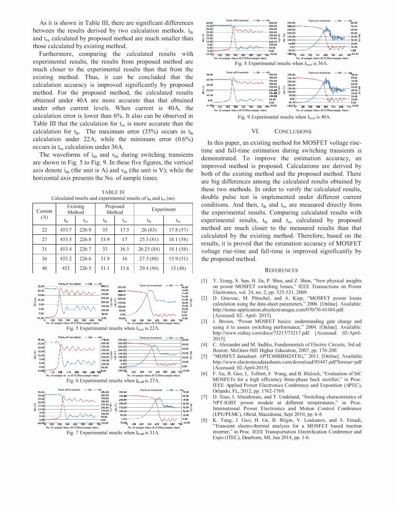
Furthermore, comparing the calculated results with experimental results, the results from proposed method are much closer to the experimental results than that from the existing method. Thus, it can be concluded that the calculation accuracy is improved significantly by proposed method. For the proposed method, the calculated results obtained under 40A are more accurate than that obtained under other current levels. When current is 40A, the calculation error is lower than 6%. It also can be observed in Table III that the calculation for tru is more accurate than the calculation for tfu. The maximum error (35%) occurs in tfu calculation under 22A; while the minimum error (0.6%) occurs in tru calculation under 36A.
The waveforms of ids and Vds during switching transients are shown in Fig. 5 to Fig. 9. In these five figures, the vertical axis denote ids (the unit is A) and Vds (the unit is V); while the horizontal axis presents the No. of sample times.
TABLE III Calculated results and experimental results of tfi' and tm (ns)
Existing Proposed Experiment Current Method Method
(A) tfa tru tft, tru tfu tm
22 453.7 226.9 35 17.5 26 (83) 17.8 (57)
27 453.5 226.8 33.9 17 25.3 (81) 18.1 (58)
31 453.4 226.7 33 16.5 26.25 (84) 18.1 (58)
36 453.2 226.6 31.9 16 27.5 (88) 15.9 (51)
40 453 226.5 31.1 15.6 29.4 (94) 15 (48)
350.00 Turn-on transirm -ids -\'dls.oo 350.00
,t-_-+-=--"---"--'IL-'''--'"'-----j JOO.OO 300.00-_=c-T, ,------i j�::: 250.00�--*--\-------i30.00
f----i-+---c-c-----1 ���:�� ! � ���:�� iZ::: ! � 5.00 150.00 -$ � 100.00 15.00 2:; 0.00 100.00 0 00 10.00 -5.00t-----;f---"--------j SO.OO
50:00 __ L----'cr"'n-r�,.__jZ:�� -to 000 100 200 300 400 500 600 700°·00 -50 0 °0 100 200 300 400 SOO 600 7005.00
No. ofsample times (O.3125nsisample time) No. ofsampl(' times (O.3125nsfsampl(' timr) Fig. 5 Experimental results when Ilo'd is 22A.
Turn-olTtransi('ut -ids -vds 30.00',------=-::�'-=='-------'C'----__;450.00 350.0 25.00 400.00 300.0 20.00 350.00 250.0
< 15.00 ���:�� � � ���:� ';' 10.00 200.00<'; 100.0 ::: 5.00 150.00'-' ;' 50.0
0 0 0 0 0 0 0 0.00 100.00 0.0 0
-5.00 50.00 -50.00 -100.0 "i;
No. ofsamplr tilurs (0.3125I1sfsamplr timr) 100
Turn on transirnl Ids vds - -
II
200 300 400 SOO
�
60.00 50.00 0.00 O.ooij:
4 3 2 I O.OO� 0.00
0.00 6 0 700-10.00
No. ofslImplr times (0.3125I1sfsample t1mr) Fig. 6 Experimental results when II""d is 27 A.
Turn-offtrllnsient -ids -\'ds Turn·on transient -ids -\'ds 35 00[t:5 450 00 350.00 70.00 30 00 -- __ 400 00 30000r--_","- 60.00 25 00 - ... 350 00 250001------'II"""';------j50.00 <' 20 00 - ��� �� � >- 200 00 40.00 a:
� :� �� ��� ��3 i !�� �� ��:: � 5_ 100 00 0 00 50 00 50 00 10.00
-��'=b 100 200 300 400 500 600 700�5'::00 _5:.001-�""'20-0 - 3- 0-
0----l.c7' SO�� 0ur--170 �;�OO No. ofslImplr times (0.3125I1s/slImple time) No. ofslImplr times (0.3125ns/slImplr time)
Fig. 7 Experimental results when II""d is 31A.
Turn-offtrllnsient -ids -\'ds 40.00 450.00 35.00 400.00 30.00 350.00 25.00 300.00 <' 20.00 2SO.00 �
';;;' 15.00 200.00� :E 10.00 150.00 .::5
5.00 100.00 0.00 SO.OO -5.00 0.00
-IO.OI\)-----rOO----yOO----yOO�Oll-----sO-O_____wll______rO -50.00 No. ofslImplr times (0.3125ns/slimple time)
Turn·on transient -ids -\'ds 3SO.00 110.00 300.00--_=-,.------j70.00 250.00 60.00
C" 200.00 50.00 _. G lSO.00 40.00 � i! 100.00 30.00 �
50.00"-==::::;:;==::1.=;;;:;::;:;;;::::1 20.00 O.OOl- 10.00
-;��:��� 2�OO������7..!00����00 No. ofslImplr times (0.3125ns/slImplr time)
Fig. 8 Experimental results when Ilo'd is 36A.
Turn-offtrllnsient -ids -\'ds 50.00 40.00_�-"1\
450.00 400.00 350.00 300.00 250.00� 30.00
1-----14--------1200.00� 1-_---f--\-____ ---1 :��:�� .::5
P-c..f ........ --...--' 50.00
3SO.00 Turn·on transient -ids -\'dbo.oo 3oo.oot-� ....... =----t..-----f80.00 250.00 70.00
� �=::: ��:�� a: .; 100.00 ��:�� � .. 50.00 20.00
0.00 Iic--"",, ,,,,--,,..---c"'--"SMO ---"60'" 0 - 7ml.0 -SO.OO
10.00 0.00
""''"''-y,; ...... ..-7000� 7ml.O -10.00 No. ofslImplr times (0.3125ns/slImplr time) No. ofslImplr times (0.3125ns/slimple time)
Fig. 9 Experimental results when Ilo'd is 40A.
VI. CONCLUSIONS
In this paper, an existing method for MOSFET voltage risetime and fall-time estimation during switching transients is demonstrated. To improve the estimation accuracy, an improved method is proposed. Calculations are derived by both of the existing method and the proposed method. There are big differences among the calculated results obtained by these two methods. In order to verify the calculated results, double pulse test is implemented under different current conditions. And then, tfu and tru are measured directly from the experimental results. Comparing calculated results with experimental results, tfu and tru calculated by proposed method are much closer to the measured results than that calculated by the existing method. Therefore, based on the results, it is proved that the estimation accuracy of MOSFET voltage rise-time and fall-time is improved significantly by the proposed method.
REFERENCES
[I] Y. Xiong, S. Sun, H. lia, P. Shea, and Z. Shen, "New physical insights on power MOSFET switching losses," IEEE Transactions on Power Electronics, vol. 24, no. 2, pp. 525-531,2009.
[2] D. Graovac, M. Piirschel, and A. Kiep, "MOSFET power losses calculation using the data-sheet parameters," 2006. [Online]. Available: http://notes-application.abcelectron ique. comiO 70/70-414 84. pdf. [Accessed: 02- April- 2015].
[3] l. Brown, "Power MOSFET basics: understanding gate charge and using it to assess switching performance," 2004. [Online]. Available: http://www.vishay.comldocs/73217/73217 .pdf. [Accessed: 02-April-2015].
[4] C. Alexander and M. Sadiku, Fundamentals of Electric Circuits, 3rd ed. Boston: McGraw-Hill Higher Education, 2007, pp. 176-200.
[5] "MOSFET datasheet: APTC60BBM24T3G," 2011. [Online]. Available: http://www.electronicsdatasheets.comldownloadl93447.pdf?format=pdf [Accessed: 02-April-20 15].
[6] F. Xu, B. Guo, L. Tolbert, F. Wang, and B. Blalock, "Evaluation of SiC MOSFETs for a high efficiency three-phase buck rectifier," in Proc. IEEE Applied Power Electronics Conference and Exposition (APEC), Orlando, FL, 2012, pp. 1762-1769.
[7] D. Xiao, L Abuishmais, and T. Undeland, "Switching characteristics of NPT-IGBT power module at different temperatures," in Proc. International Power Electronics and Motion Control Conference (EPE/PEMC), Ohrid, Macedonia, Sept 20 I 0, pp. 6-8.
[8] K. Yang, 1. Guo, H. Ge, B. Bilgin, V. Loukanov, and A. Emadi, "Transient electro-thermal analysis for a MOSFET based traction inverter," in Proc. IEEE Transportation Electrification Conference and Expo (ITEC), Dearborn, MI, lun 2014, pp. 1-6.