Imprint Mask Course 2017-10-03 - Resnick · Canon Nanotechnologies, Inc. Claymore: 32nm Programmed...
60
Canon Nanotechnologies, Inc. Mask Replication The lifetime of a mask is anticipated to be ~ 50,000 – 100,000 imprints An e-beam written master mask will cost ~ $500K If you wanted to print 1M wafers, you would spend ~ $500M on masks Go share that strategy with a fab manager!!! The solution: create a Master Template that can easily be replicated Master Daughter approach Good news! You can use an imprinter to make the Daughter Templates
Transcript of Imprint Mask Course 2017-10-03 - Resnick · Canon Nanotechnologies, Inc. Claymore: 32nm Programmed...

Canon Nanotechnologies, Inc.Canon Nanotechnologies, Inc.
Mask Replication
The lifetime of a mask is anticipated to be ~ 50,000 – 100,000 imprints
An e-beam written master mask will cost ~ $500K
If you wanted to print 1M wafers, you would spend ~ $500M on masks
Go share that strategy with a fab manager!!!
The solution: create a Master Template that can easily be replicatedMaster Daughter approachGood news! You can use an imprinter to make the Daughter Templates
Canon Nanotechnologies, Inc.Canon Nanotechnologies, Inc.
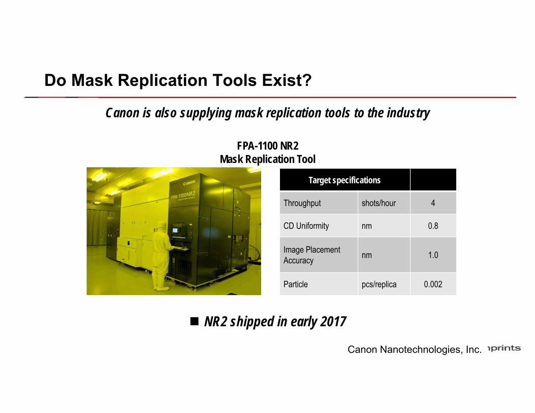
Do Mask Replication Tools Exist?
Canon is also supplying mask replication tools to the industry
FPA-1100 NR2Mask Replication Tool
Target specifications
Throughput shots/hour 4
CD Uniformity nm 0.8
Image PlacementAccuracy nm 1.0
Particle pcs/replica 0.002
NR2 shipped in early 2017

Canon Nanotechnologies, Inc.Canon Nanotechnologies, Inc.
Replication Example: Semiconductor
a) Master Imprint
b) Replica Mask
28nm 48nm32nm
32nm28nm 48nm

Canon Nanotechnologies, Inc.Canon Nanotechnologies, Inc.
Replication and Image Placement
During replication, all the usual parameters need to be controlled, in addition to just feature resolution– Defectivity– Critical dimension uniformity– Image placement
The data below indicates that final image placement can be as low as 2.5nm
Master/Replica @ 2x nm Target 2015
Defectivity (pcs/cm2) 1.0 0.6
CD Uniformity (3σ, nm) 2.2 1.5
Image Placement (nm, 3s) 2.5 2.5
Replica Image Placement
X : 2.00nmY : 2.48nm
Courtesy DNP

Canon Nanotechnologies, Inc.Canon Nanotechnologies, Inc.
What’s Left? I can write the mask I can etch the mask I can replicate the maskAnd I’ve satisfied requirements for CDU, IP and defectivity I’m done, right???
NO!! Masks must be perfect. No defects can exist in a critical area of the mask. As a result, the mask must be
InspectedRepaired
Imprint lithography is challenged by the fact that it is a 1x technology. This makes inspection and repair more difficult

Canon Nanotechnologies, Inc.Canon Nanotechnologies, Inc.
Inspection Methods
Optical Inspection - Mask– KLA-Tencor: – Reflection/Transmission Mode
Electron Beam Inspection - Wafer– Die-to-DieKLA-Tencor eS35HMI eScan315
– Die-to-DatabaseNGR2100
eS35
6xx
Defect size, patterned template (nm) [V] 35 30 30 20 20 20 20 10
Year of Production 2008 * 2009 2010 2011 2012 2013 2014 2015
DRAM ½ pitch (nm) (contacted) 59 52 45 40 36 32 28 25Flash ½ pitch (nm) (un-contacted poly) 45 40 36 32 28 25 22 20Defect size, patterned template (nm) [V] 35 30 30 20 20 20 20 10
Year of Production 2008 * 2009 2010 2011 2012 2013 2014 2015
DRAM ½ pitch (nm) (contacted) 59 52 45 40 36 32 28 25Flash ½ pitch (nm) (un-contacted poly) 45 40 36 32 28 25 22 20
eScan315

Canon Nanotechnologies, Inc.Canon Nanotechnologies, Inc.
Claymore: 32nm Programmed defect layout
All sections (32nm, 40nm, and 48nm) have the same corner marks and unit cell step distances
– X = 2um, Y = 3um
32 nm 40nm and 48nm feature types are the same design with different dummy shrinks. 228um
162um
48nm section
40nm section
32nm section
Line / space
Pillar array
SRAM M1
Line / space
Pillar array
SRAM M1
Line / space
Pillararray
SRAM M1
M1 Contact L/S

Defect locations
Biggest Smallest
Mouse Bite
Extensions
14um
Three repeats of each set
Labeled 12 to 1
Separation between PD types
Separation between PD Sizes
6m
Vertical
Horizontal
Vertical
Horizontal
32nm section
Line spacefeatures
Other features types have a similar array of defects Programmed defects sizes are
arrayed every 7 unit cells horizontally
Programmed defect types are arrayed every other unit cell vertically

Canon Nanotechnologies, Inc.Canon Nanotechnologies, Inc.
Programmed Defects for 32nm Patterns
32x48nm32x32nm4x32nm
M1
L/S
Contact
Programmed defects start at 4nm and increase in increments of 4nm up to 48nm

Canon Nanotechnologies, Inc.Canon Nanotechnologies, Inc.
Mask and Imprint Analysis
SEMs of the Mask were captured with a Holon EMU-270A SEM– 1.5 nm resolution at 1.0 kV when
applying aberration correction. – Low vacuum and charge control enable
high quality imaging on fused silica masks.
Images of the imprints taken with a JEOL JSM-6340F field emission cold cathode SEM – 1.2 nm resolution capability at 15 kV and
2.5nm at 1 kV.

Canon Nanotechnologies, Inc.Canon Nanotechnologies, Inc.
32 nm Half Pitch LinesMask
Imprint
1 2 3 4 5 6
7 8 9 10 11 12
20nm

Canon Nanotechnologies, Inc.Canon Nanotechnologies, Inc.
PD measured area evaluation process
Smoothing &Threshold segmentation
Image Shift by pitch
Image A
Image B
Image A - Image B
Count white pixels and convert to area 2349 nm2
DAFC – Defect Analysis for the Financially Challenged

Canon Nanotechnologies, Inc.Canon Nanotechnologies, Inc.
0
200
400
600
800
1000
1200
1400
1600
0 500 1000 1500 2000
Data Size (nm^2)
Mea
sure
d PD
are
a (n
m^2
)
Imprint Template
Measured area compared to data size
0
200
400
600
800
1000
1200
1400
1600
0 500 1000 1500 2000
Data Size (nm^2)
Mea
sure
d PD
are
a (n
m^2
)
Imprint Template
Mid-line extension Shrinking Pillar
Canon Nanotechnologies, Inc.Canon Nanotechnologies, Inc.
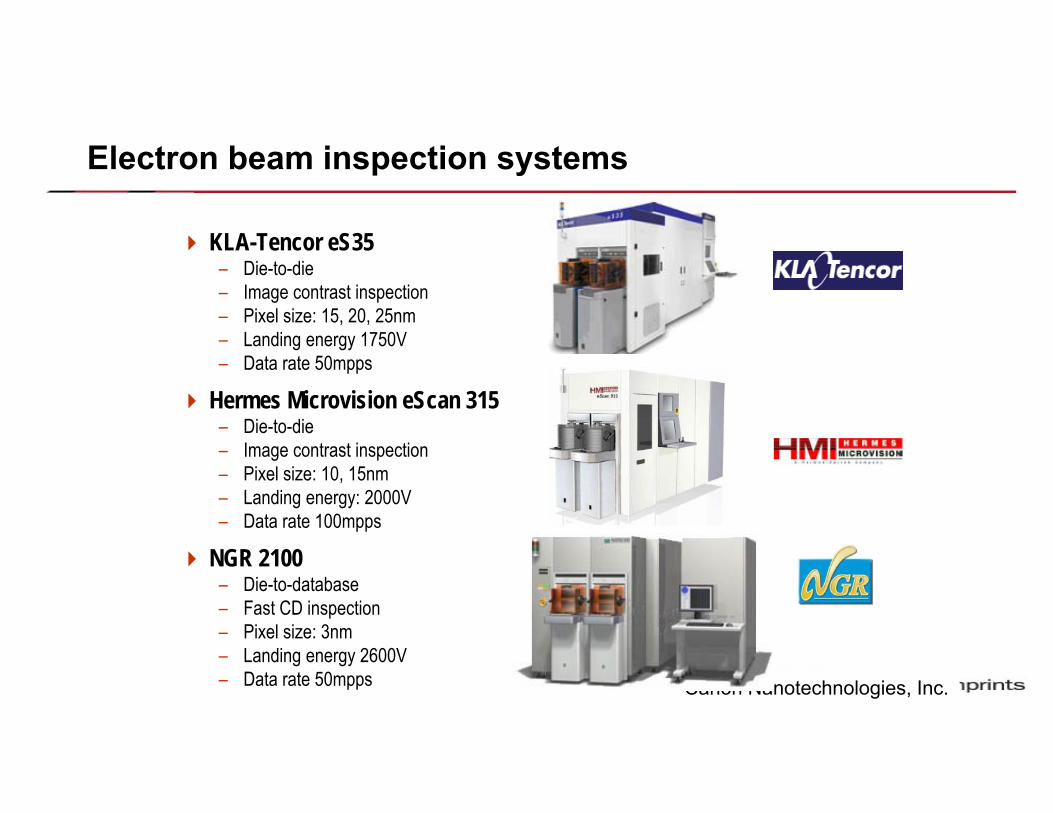
Electron beam inspection systems
KLA-Tencor eS35– Die-to-die– Image contrast inspection– Pixel size: 15, 20, 25nm– Landing energy 1750V– Data rate 50mpps
Hermes Microvision eScan 315– Die-to-die– Image contrast inspection– Pixel size: 10, 15nm– Landing energy: 2000V– Data rate 100mpps
NGR 2100– Die-to-database– Fast CD inspection– Pixel size: 3nm– Landing energy 2600V– Data rate 50mpps

Canon Nanotechnologies, Inc.Canon Nanotechnologies, Inc.
Programmed defect pixel progression
12500
12600
12700
12800
12900
13000
13100
13200
13300
16000 16020 16040 16060 16080 16100 16120 16140 16160 16180 16200
x-loc (um)
y-lo
c (u
m)
PD_Loc
12 11 10 9 8 7 6 5 4 3 2 1
48nm
40nm
32nm
Big Small
Programmed Defects
12500
12600
12700
12800
12900
13000
13100
13200
13300
16000 16020 16040 16060 16080 16100 16120 16140 16160 16180 16200
x-loc (um)
y-lo
c (u
m)
PD_Loc 25nm Pixel
12 11 10 9 8 7 6 5 4 3 2 1
48nm
40nm
32nm
Programmed Defects
12500
12600
12700
12800
12900
13000
13100
13200
13300
16000 16020 16040 16060 16080 16100 16120 16140 16160 16180 16200
x-loc (um)
y-lo
c (u
m)
PD_Loc 20nm Pixel 25nm Pixel
12 11 10 9 8 7 6 5 4 3 2 1
48nm
40nm
32nm
Programmed Defects
12500
12600
12700
12800
12900
13000
13100
13200
13300
16000 16020 16040 16060 16080 16100 16120 16140 16160 16180 16200
x-loc (um)
y-lo
c (u
m)
PD_Loc 15nm Pixel 20nm Pixel 25nm Pixel
12 11 10 9 8 7 6 5 4 3 2 1
48nm
40nm
32nm
Programmed Defects
Setup errors
(6nm)
(5nm)
(4nm)

Canon Nanotechnologies, Inc.Canon Nanotechnologies, Inc.
32nm Features 15nm Pixel Inspection
0%
20%
40%
60%
80%
100%
0 5 10 15 20 25 30 35 40Data Size (nm)
Cap
ture
Pro
babi
lity
(%)
Shrinking pillar SRAM_mid-line ext
2
1
32nm Features 15nm Pixel Inspection
0%
20%
40%
60%
80%
100%
0 5 10 15 20 25 30 35 40Data Size (nm)
Cap
ture
Pro
babi
lity
(%)
Shrinking pillar SRAM_mid-line ext
2
32nm Features 15nm Pixel Inspection
0%
20%
40%
60%
80%
100%
0 5 10 15 20 25 30 35 40Data Size (nm)
Cap
ture
Pro
babi
lity
(%)
Shrinking pillar SRAM_mid-line ext
2
1
80% capture rate examples
2
1
The sensitivity range is 10 to 18nm for an 80% capture rate
32nm Features 15nm Pixel Inspection
0%
20%
40%
60%
80%
100%
0 160 320 480 640 800 960 1120 1280Measure PD area (nm^2)
Cap
ture
Pro
babi
lity
(%)
Shrinking Pillar SRAM mid-line Ext
578nm^2~18nm PD
327nm^2~10nm PD 2
1
32nm Features 15nm Pixel Inspection
0%
20%
40%
60%
80%
100%
0 160 320 480 640 800 960 1120 1280Measure PD area (nm^2)
Cap
ture
Pro
babi
lity
(%)
Shrinking Pillar SRAM mid-line Ext
578nm^2~18nm PD
327nm^2~10nm PD 2
1

Canon Nanotechnologies, Inc.Canon Nanotechnologies, Inc.
eScan 315: e-beam wafer inspection48 44 40 36 32 28 24 20 16 12 8 4 nm
10nmpixel
15nmpixel
Metal-1
Pillar
Lines
VMHMVEHEVMHMVEHEVMHMVEHE
VMHMVEHEVMHMVEHEVMHMVEHE
VMHMVEHEVMHMVEHEVMHMVEHE
32nm HP Parameters:100 MPPS
2000V3nA

Canon Nanotechnologies, Inc.Canon Nanotechnologies, Inc.
Captured Programmed Defects: 10nm Pixel
Metal-1 Pillars LinesProgrammed defects: 8nm – 12nm
Mousebite 8nm
8nm
Mid Extension
Line Shortening
Line Extension
8nm
8nm V Extension
H Extension
V Mousebite
H Mousebite 8nm
8nm
8nm
8nm V Extension
V Mousebite
12nm
12nm
12nm
H Mousebite
H Extension 12nm

Canon Nanotechnologies, Inc.Canon Nanotechnologies, Inc.
KLA-T 6xx Optical Inspection Results
Because the background noise is low, it is possible to discern the defect without resolving the 32nm pattern.
The KLA-T 6xx platform works in both Transmitted and Reflected light modes.
Transmitted and Reflected Light capture different types of defects. Having both modes essential for capturing critical defects.
In these examples, one defect in the 32nm half pitch pattern has signal in transmitted and one in reflected mode.
Inspection of 32nm half pitch patternsDifference Reference PD Cell
Tran
smitte
dTr
ansm
itted
Refle
cted
Refle
cted
Def#1
Def#2

Canon Nanotechnologies, Inc.Canon Nanotechnologies, Inc.
Modulation vs. Programmed defect size
Modulation tracks well with the measured defect size in the maskSensitivity is on the order of 32nmThresholds can be optimized to increase sensitivity
0
200
400
600
800
1000
1200
1400
1600
0 500 1000 1500 2000
Data Size (nm^2)
Mea
sure
d PD
are
a (n
m^2
)
Imprint Template
Measured defect size vs. coded defect size Modulation vs. defect size during 6xx inspection
Modu
lation
Defect size (nm)
40
35
30
25
20
15
10
5
018 26 30 36 42 48 54 60 66 72
Data Size (nm2)
Meas
ured
PD
area
(nm2 )

Canon Nanotechnologies, Inc.
Infrastructure: Template RepairRaveLLC Nawotec
Nanomachining system E-beam Deposition/Etch

Canon Nanotechnologies, Inc.300 nm defect 50 nm defect 50 nm trench
QuartzLine
Quartzdefect
After AFMrepair
Before repair
Repair ExamplesAfter repair on a RaveLLC 650nm system
Canon Nanotechnologies, Inc.Canon Nanotechnologies, Inc.
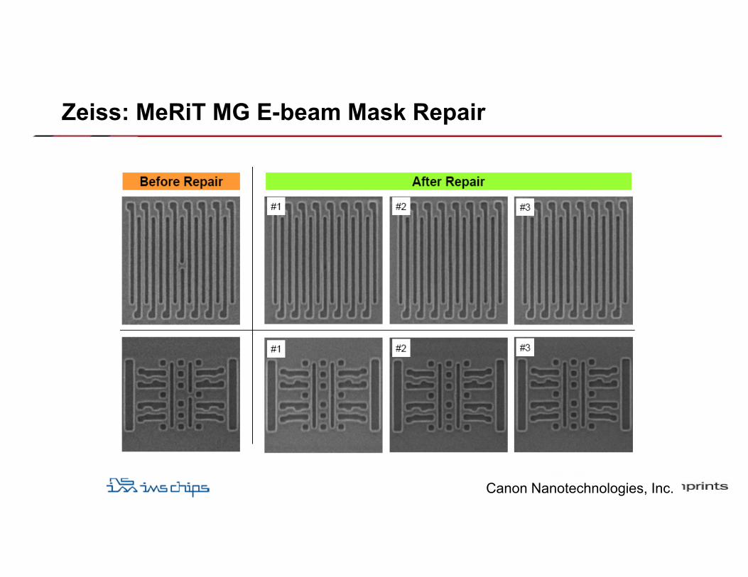
Zeiss: MeRiT MG E-beam Mask Repair

Canon Nanotechnologies, Inc.Canon Nanotechnologies, Inc.
Repairs: After Imprint
40nm
32nm

Canon Nanotechnologies, Inc.Canon Nanotechnologies, Inc.
So is this this technology really going to work?
Canon Nanotechnologies, Inc.
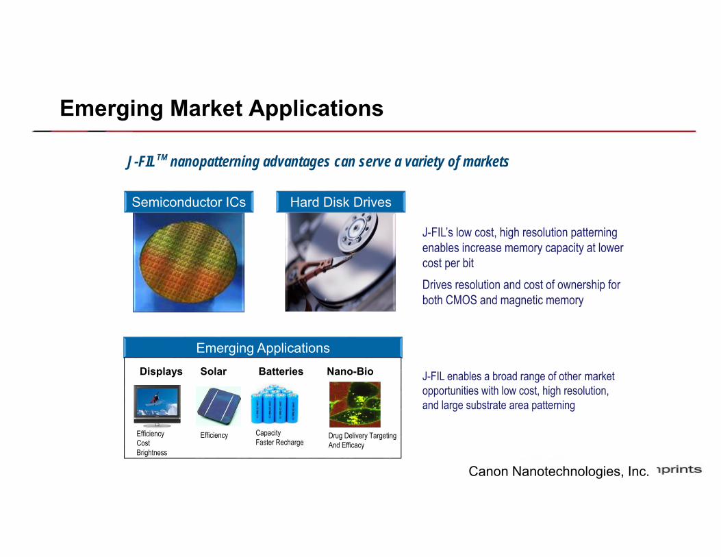
Emerging Market Applications
Emerging Applications
J-FILTM nanopatterning advantages can serve a variety of markets
J-FIL’s low cost, high resolution patterning enables increase memory capacity at lower cost per bitDrives resolution and cost of ownership for both CMOS and magnetic memory
J-FIL enables a broad range of other market opportunities with low cost, high resolution, and large substrate area patterning
Hard Disk DrivesSemiconductor ICs
Displays Solar Batteries Nano-Bio
EfficiencyCostBrightness
Efficiency CapacityFaster Recharge
Drug Delivery TargetingAnd Efficacy

Canon Nanotechnologies, Inc.Canon Nanotechnologies, Inc.
Full Wafer/Disk Imprint Process
Imprio 1100 (Photonic Crystals)
Thin Template
150mm Diameter Patterned Media Template
Imprio HD7000 (Patterned Media)

Canon Nanotechnologies, Inc.Canon Nanotechnologies, Inc.
Hard Drives
Hard disk drives operate by storing bits of information on a disk coated with a magnetically influenced film– Magnetic media
These things have been working for years. What’s the problem?

Canon Nanotechnologies, Inc.Canon Nanotechnologies, Inc.

Canon Nanotechnologies, Inc.Canon Nanotechnologies, Inc.
10
100
2004 2006 2008 2010 2012 2014 2016 2018 2020
MPUDRAMFlashStorage
Hal
f Pitc
h
Year
Why Imprint Lithography for Patterned Media? Let’s compare the Information storage roadmap against the
well established ITRS Roadmap for integrated circuits
The Storage Roadmap is much more aggressive than the ITRS Roadmap
High volume optical tools will not be available in time
The price of an EUV printing tool is prohibitive (~$50-75M)
Electron beam writers have the resolution, but not the throughput
Imprint offers the best combination of cost, throughput and resolution
193n
mN
ext G
ener
atio
n Li
thog
raph
y
193i – no resolutionEUV $$$, timing for 1TbEBDW – Low throughput
UV-IL –right combination
1Tb/in2
100
70
40
20
10
5
$90-100M$100-150M
Canon Nanotechnologies, Inc.Canon Nanotechnologies, Inc.
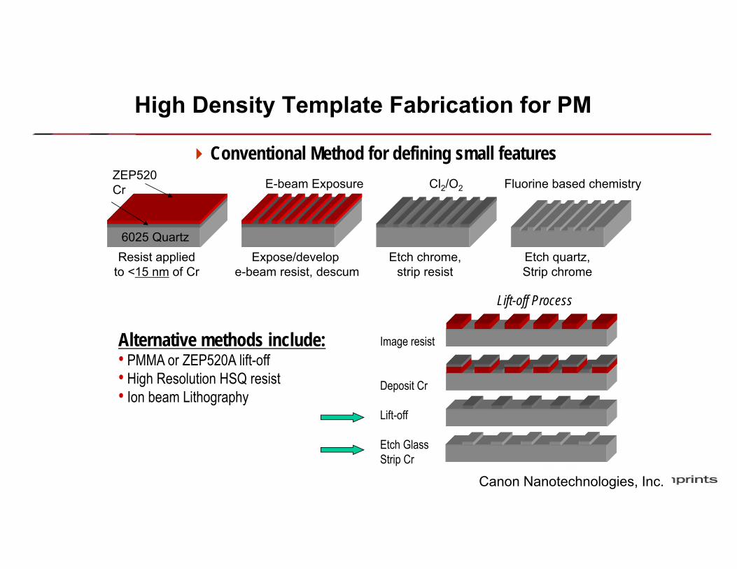
High Density Template Fabrication for PM
Conventional Method for defining small features
Resist appliedto <15 nm of Cr
Expose/develop e-beam resist, descum
Etch chrome,strip resist
Etch quartz,Strip chrome
6025 Quartz
ZEP520Cr E-beam Exposure Cl2/O2 Fluorine based chemistry
Alternative methods include:• PMMA or ZEP520A lift-off• High Resolution HSQ resist• Ion beam Lithography
Lift-off Process
Image resist
Deposit Cr
Lift-off
Etch GlassStrip Cr

Canon Nanotechnologies, Inc.
Template Mastering with Rotary E-beam
Fabrication of Master Templates for Patterned Media requires high resolution patterning over large areasSub-50 nm resolutionVery low pattern distortion
Patterns are concentric lines, arcs, and dot arrays
Master template
Electron Gun
Rotating Spindle Stage
Linear Stage Rotational speed: ~ 100 to 3000 rpmDirection: CW or CCWLinear translation in one radial direction
Canon Nanotechnologies, Inc.Canon Nanotechnologies, Inc.
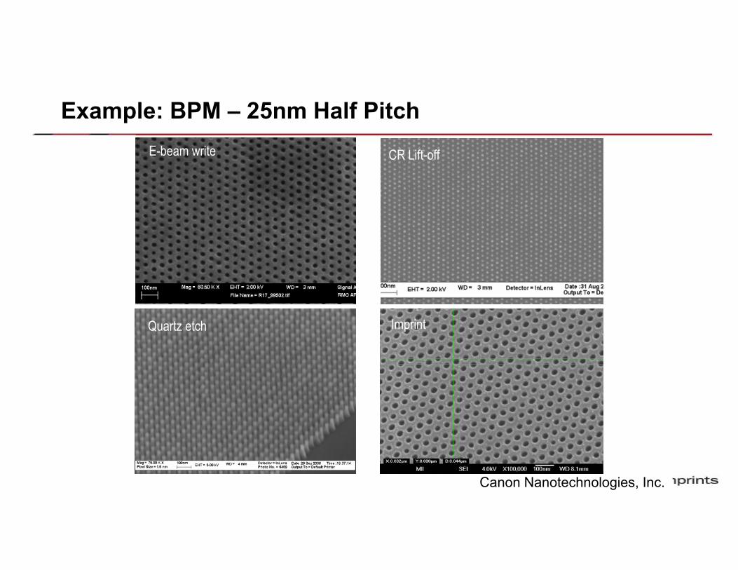
Example: BPM – 25nm Half Pitch
25nm half-pitch (250 Gb/in2)
E-beam write
ImprintQuartz etch
CR Lift-off
Canon Nanotechnologies, Inc.Canon Nanotechnologies, Inc.
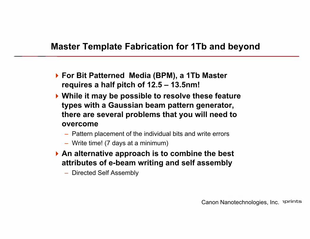
Master Template Fabrication for 1Tb and beyond
For Bit Patterned Media (BPM), a 1Tb Master requires a half pitch of 12.5 – 13.5nm!
While it may be possible to resolve these feature types with a Gaussian beam pattern generator, there are several problems that you will need to overcome– Pattern placement of the individual bits and write errors– Write time! (7 days at a minimum)
An alternative approach is to combine the best attributes of e-beam writing and self assembly– Directed Self Assembly
Canon Nanotechnologies, Inc.Canon Nanotechnologies, Inc.
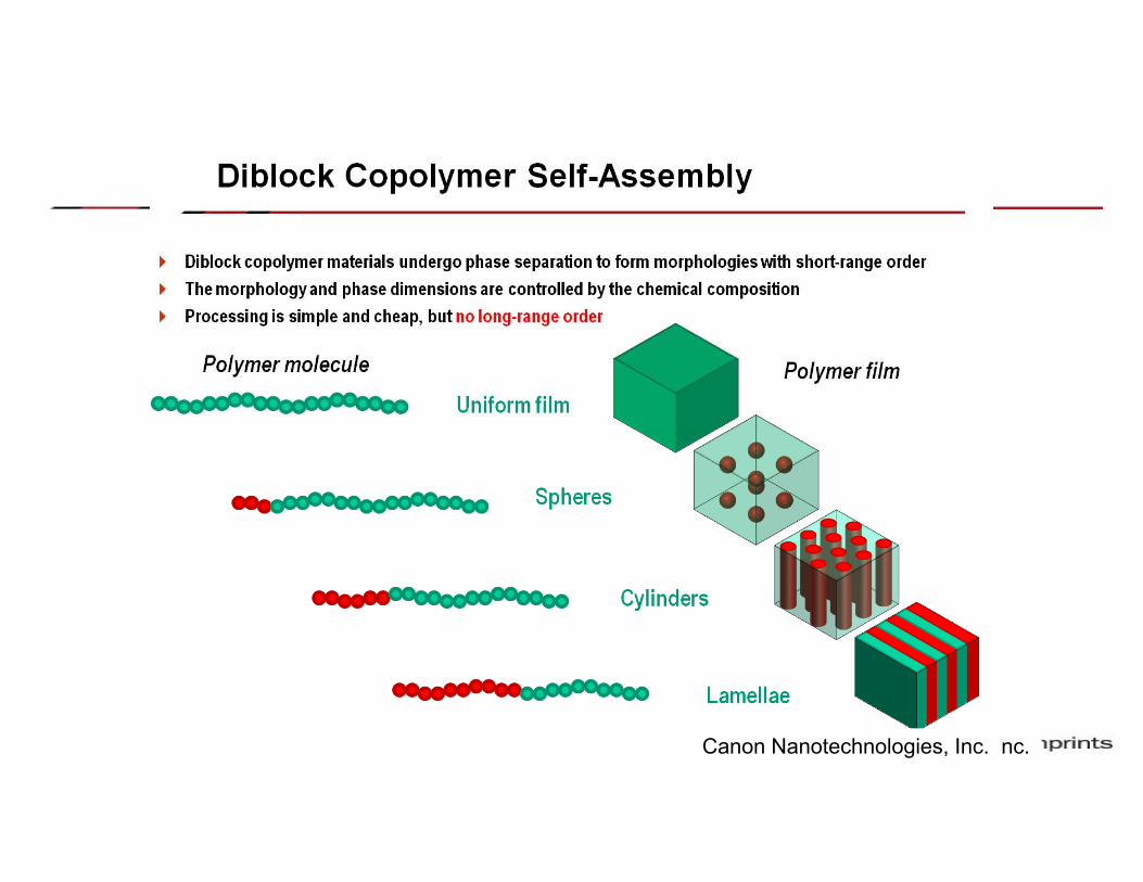
Diblock copolymer materials undergo phase separation to form morphologies with short-range order The morphology and phase dimensions are controlled by the chemical composition Processing is simple and cheap, but no long-range order
Uniform film
Spheres
Cylinders
Lamellae
Polymer molecule Polymer film
Canon Nanotechnologies, Inc.

Canon Nanotechnologies, Inc.Canon Nanotechnologies, Inc.
Examples: Short-range order
From Joy Cheng, IBM Almaden
Cylinders
Lamellae
Polymer solution is spincoated on an unpatterned substrate and then annealed for several minutes.
~1 micron
~1 micron
Uniform feature size and pitch, but no long-range order.
(Likely okay for PV applications)
PS-b-PMMA

Canon Nanotechnologies, Inc.Canon Nanotechnologies, Inc.
Directed Self Assembly
To achieve long range order, we can use the e-beam writer to “guide” the placement of the block copolymer
Pattern Rectification Density Multiplication
Half pitch = 13.5nm

Canon Nanotechnologies, Inc.Canon Nanotechnologies, Inc.
Another DSA Example

Template InspectionCandela X-Beam™ Optical Surface Analyzer
CircumferentialLaser
RadialLaser
Polarizer
Combination phase and specular detectorScattered light
detector
Rotating spindle stage
= 408 nm
= 408 nm
Multi-channel inspection of optical propertiesScattered light dark fieldReflected light bright field, reflectometryPhase shift thin film measurements
This work:Candela 6120: disk substratesCandela CS20: templates
Canon Nanotechnologies, Inc.

Identifying Defects on Templates and Disks
Imprint A Imprint BTemplate
• There are 3 critical defects that need to be tracked: template, particle, non-fill• How do we identify each defect type (defect classification)?• How do we track defectivity?
- From template to disk- From disk to disk
Specular Inspection
Canon Nanotechnologies, Inc.

Canon Nanotechnologies, Inc.Canon Nanotechnologies, Inc.
Defect Source Analysis
Total inspected area: ~ 29 cm2
Total defectivity: ~ 2.4 def/cm2
Defec
t Cou
nt

Canon Nanotechnologies, Inc.Canon Nanotechnologies, Inc.
Liquid Crystal Display Panel Fabrication
LCD displays are ubiquitous:
LCD Panel Components

Nanoscale Patterning Can Improve Many Critical Components in Displays
J-FILTM can offer improved technologies at lower cost that impacts approximately 50% of liquid crystal display Bill of Materials (BoM).

Canon Nanotechnologies, Inc.Canon Nanotechnologies, Inc.
LithoFlex 350TM
SYSTEM CONFIGURATION
Plate-to-Roll (P2R) or Roll-to-Plate (R2P) Template Substrates:
– P2R < 300mm glass or silicon wafer – R2P < 350mm width web Automated or manual template loading Automatic protective film particle control UV cure (365nm) light source PERFORMANCE Sub-50 nanometer feature resolution Throughput >1 meter per minute Position accuracy of 600 microns (3)
– Alignment Option Available Print width: 300mm maximum
LithoFlex 350
TECHNOLOGYJet and FlashTM imprint technology IntelliJetTM resist jetting dispensing system

Canon Nanotechnologies, Inc.Canon Nanotechnologies, Inc.
Plate to Roll (P2R) imprinting
P2R imprinting uses patterned rigid substrates:– As an example, a 300mm wafer can be used as the working template
• Can be patterned several different ways:- Photolithography- Imprint Lithography- Electron beam Lithography- Photo or E-beam/DSA

Canon Nanotechnologies, Inc.Canon Nanotechnologies, Inc.
J-FIL Results
350mm web with protective film
Pattern close-up
Protective film removed

Canon Nanotechnologies, Inc.Canon Nanotechnologies, Inc.
Test Pattern SEM images
Both micron size and nanoscale patterns can be imprinted within the same field
Micron scale pattern 450nm test pattern
Canon Nanotechnologies, Inc.Canon Nanotechnologies, Inc.
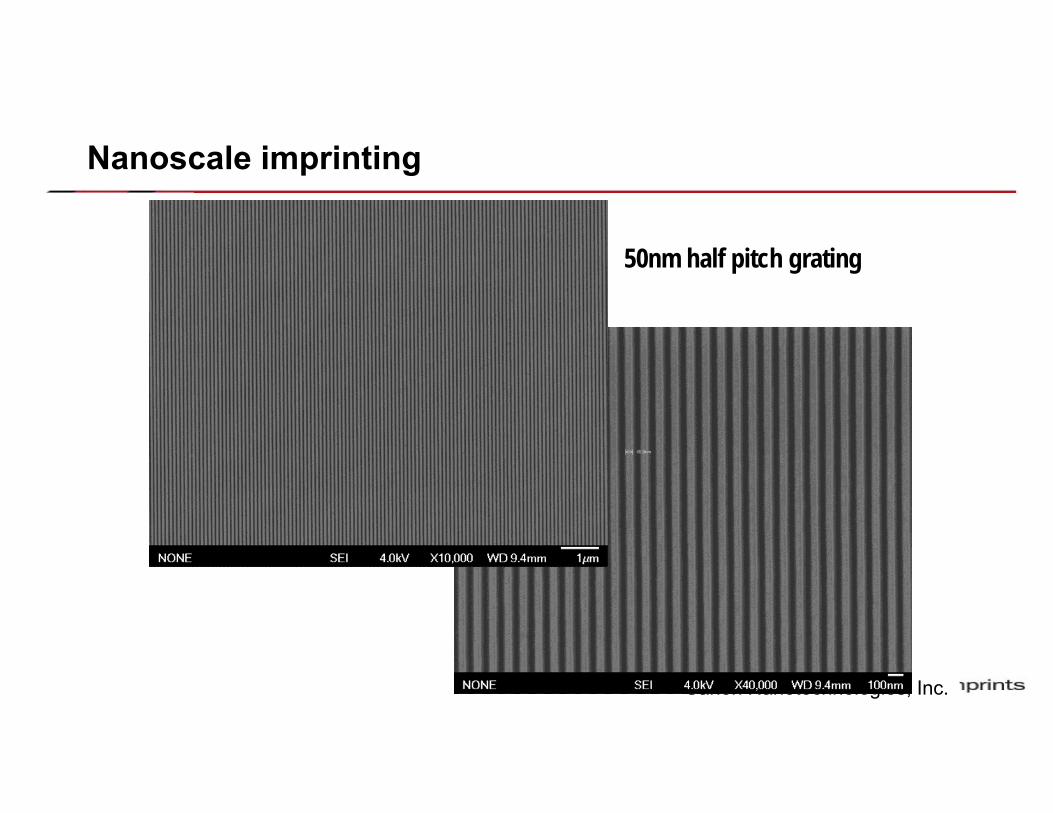
Nanoscale imprinting
50nm half pitch grating

Canon Nanotechnologies, Inc.Canon Nanotechnologies, Inc.
Wire Grid Polarizers
Two methods for fabricating Wire Grid Polarizers(WGPs):
Very low cost Very High PerformanceAl
Resist
Template
Imprint
WGP
Glass Substrate
Al
ResistResidual layer
Al

Canon Nanotechnologies, Inc.Canon Nanotechnologies, Inc.
Etched WGP Results
Performance is driven by many factors– Defectivity– Pitch – Duty Cycle– Aspect Ratio– Al quality
Integrated Transmittance : ~44%Extinction ratio at 550nm: ~50K

Final Thoughts
X-ray Lithography1X proximity-based technology usinga membrane-based mask
Ion Beam Lithography1X and projection technology usinga stencil-based mask
SCALPELProjection electron lithography usinga thin membrane mask
1. I worked on all three mask technologies
PrXL
SCALPEL
IBL
2. From a manufacturing perspective, all three are now dead3. All three died, in part, from a lack of mask infrastructure

Canon Nanotechnologies, Inc.
AcknowledgmentsCNT and Molecular Imprints
Ecron Thompson, Gerard Schmid, Mike Miller, Kosta Selinidis, Ian McMackin, Cindy Brooks, Gary Doyle, Gaddi Haase, Kang Luo, Lovejeet Singh, David Curran
DNPShiho Sasaki, Nobuhito Toyama, Masaaki Kurihara, and Naoya Hayashi
MotorolaBill Dauksher, Kevin Nordquist, Kathy Gehoski, Ngoc Le, Eric Ainley, Steve Smith
KLA-TencorMark McCord
Vistec-SemiconductorTim Groves, Mike Butler, Eric Tapley, Olaf Fortagne
Photronics, Toppan Photomask, IMS Chips, NGR, LBNL, RaveLLC, Zeiss, NuFlare, Mentor Graphics, HMI
This work was partially funded by:DARPA (N66001-02-C-8011, N66001-01-1-8964) and NIST-ATP

Canon Nanotechnologies, Inc.Canon Nanotechnologies, Inc.
References
To learn more about Jet and Flash Imprint Lithography, go to:– http://www.molecularimprints.com/news-and-publications
– http://cnt.canon.com/technical-library/
Canon Nanotechnologies, Inc.Canon Nanotechnologies, Inc.
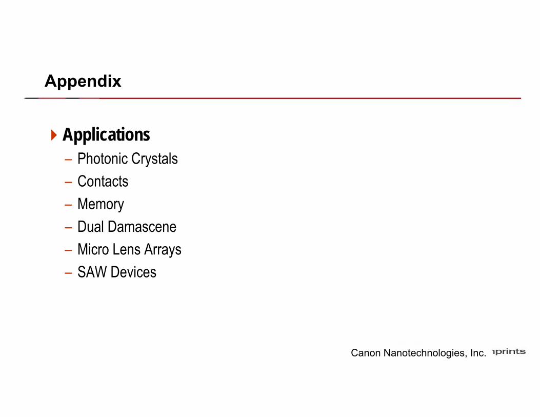
Appendix
Applications– Photonic Crystals– Contacts– Memory– Dual Damascene– Micro Lens Arrays– SAW Devices

An Example: Photonic Crystal – 80nm HPExample: Photonic Crystal Array – Pattern Transfer
After PlanarizationAfter Imprint
After Dry Develop After Cr/Glass etch

Canon Nanotechnologies, Inc.
The Complete S-FIL Process: Contacts
Template: 80 nm dense pillars
Imprinted Etch Barrier
Etched 80 nm contacts

Canon Nanotechnologies, Inc.Canon Nanotechnologies, Inc.
Hoya: 30nm IBM Memory
BOx
Si
Ox
Template Imprint
X-SectionSi Etch

Canon Nanotechnologies, Inc.
Dual Damascene
Template by Toppan Replication on ImprioTM 55, Willson et al. at UT.
met
al le
vels
met
al le
vels via levels
via levels
Canon Nanotechnologies, Inc.Canon Nanotechnologies, Inc.
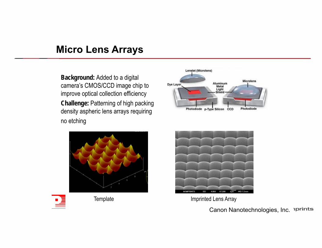
Micro Lens Arrays
Template Imprinted Lens Array
Background: Added to a digital camera’s CMOS/CCD image chip to improve optical collection efficiencyChallenge: Patterning of high packing density aspheric lens arrays requiringno etching

Canon Nanotechnologies, Inc.Canon Nanotechnologies, Inc.
SAW Device Fabrication
Step 1. Create Template
Input Output
Step 2. Imprint, etch the aluminum IDT,and remove the resist
The patterned aluminum (light grey) is 40 nm thick X 130 nm wide, and the substrate material (dark grey) is LiNbO3.
Note the line uniformity and the absence of line edge roughness in the final pattern.
Template