Implementation of a Grid Connected Solar Inverter with...
104
ECE 4600 Group Design Project Implementation of a Grid Connected Solar Inverter with Maximum Power Point Tracking by Group 03 Valeria Pevtsov Kresta Zumel Ian Swintak Radeon Shamilov Reza Fazel-Darbandi Final report submitted in partial satisfaction of the requirements for the degree of Bachelor of Science in Electrical and Computer Engineering in the Faculty of Engineering of the University of Manitoba Academic Supervisor(s) Dr. Athula Rajapakse Department of Electrical and Computer Engineering University of Manitoba Date of Submission March 10, 2014 Copyright 2014 Valeria Pevtsov, Kresta Zumel, Radeon Shamilov, Reza Fazel-Darbandi, Ian Swintak
Transcript of Implementation of a Grid Connected Solar Inverter with...

ECE 4600 Group Design Project
Implementation of a Grid Connected Solar Inverterwith Maximum Power Point Tracking
byGroup 03
Valeria Pevtsov Kresta ZumelIan Swintak
Radeon Shamilov Reza Fazel-Darbandi
Final report submitted in partial satisfaction of the requirements for the degree of
Bachelor of Science in Electrical and Computer Engineering in the
Faculty of Engineering of the University of Manitoba
Academic Supervisor(s)
Dr. Athula RajapakseDepartment of Electrical and Computer Engineering
University of Manitoba
Date of Submission
March 10, 2014
Copyright © 2014 Valeria Pevtsov, Kresta Zumel, Radeon Shamilov, RezaFazel-Darbandi, Ian Swintak


Grid Connected Solar Inverter
Abstract
This thesis aims to design and implement a grid-connected solar inverter with Maximum
Power Point Tracking. This project provides a solution to environmentally friendly power
production in residential applications. The hardware part of the system was modeled and
simulated in PSCAD. The parameters used were arrived at by performing design calculations
for each subsystem such as the DC/DC converter, DC/AC inverter, solar panels, and the
grid connection. The individual subsystems were built and tested with results proving the
intended functionality and specifications. Software development includes the algorithms
needed to operate the DC/DC converter based MPPT as well as the DC/AC inverter
and the grid connection control system. The developed software was integrated with the
hardware. As a result, the DC/DC converter was able to provide a DC bus voltage of
approximately 100V and the overall system excluding the solar panels was able to push 300
mW into the grid while maintaining synchronization. The reactive power going to the grid
was minimized to approximately 0V Ar. Overall, this report provides a technical solution
for a grid-connected solar inverter system with MPPT.
- i -

Grid Connected Solar Inverter
Contributions
This design project aims to create a system that allows for the connection of solar panels
directly to the grid. While there are systems currently available to perform this task,
our system aimed to be a lower cost alternative as well as target residential applications
specifically. To achieve this target application, our design provides an easy connection to the
grid as well as being able to support a power output that would be expected in residential
applications. The design started from nothing but the solar panels that were given to us
from the tech shop allowing us to choose the rest of the components required for the system
to provide a lower cost solution. This project was divided into several milestones as well
as broken down further into smaller tasks. Each task was completed by either individual
group member or the entire group.
Contributions to the project were also provided by the following ECE staff:
* Dr. Athula Rajapakse is our supervisor. He provided us with experience and guidance
throughout the project. He also assisted in developing the PSCAD simulation case of
the entire system.
* Erwin Dirks provided the necessary equipment, as well as advice regarding the design
of the hardware. He also provided components that were available in the department
that allowed us to keep under budget.
- ii -

Grid Connected Solar Inverter
Legend: •Lead task Contributed
Val
eria
Pev
tsov
Kre
sta
Zu
mel
Rad
eon
Sh
amil
ov
Rez
aF
aze
l-D
arb
and
i
Ian
Sw
inta
k
Literature Review
DC/DC converter •DC/AC inverter • •MPPT algorithm •Gate driver •Grid synchronization •
System Design
DC/DC converter •DC/AC inverter and filter • •Gate driver •Microcontroller Software •
Simulation
Overall system simulation • Individual Prototype Build & Test
DC/DC converter • DC/AC inverter and filter • • Microcontroller and Software •
Overall Prototype Test
Hardware Interface • •Software and hardware integration • Test and Troubleshoot - Using LabVolt DC supply and RL load • •- Applying SPWM to inverter • - Improving switching signal • •- Connecting to the grid
Final Report
Report Writing - iii -

Grid Connected Solar Inverter
Acknowledgements
We would like to thank the following people for their support in this project:
Our supervisor, Dr. Athula Rajapakse, for his guidance during the entire course of the
project. He provided us invaluable assistance in developing our PSCAD simulation
case, as well as understanding the theory behind the project.
Mr. Erwin Dirks for his general technical assistance. His insightful advice and sugges-
tions greatly helped us in choosing our components and in building and testing of our
system. He also provided us with a significant portion of the hardware components
and equipment that we used in the project.
Sinisa Janjic for ordering and providing us all the parts that we need.
Dr. Behzad Kordi and Mr. Daniel Card for coordinating the ECE 4600 course.
Aidan Topping and Rafi Mahabbat Bin Belal for their feedback on our reports.
Corey Smith for assisting us with our heat sink assembly.
Amin Hajihosseinlu for his advice in software development and troubleshooting.
Our families and friends for support and encouragement.
- iv -

Grid Connected Solar Inverter TABLE OF CONTENTS
Table of Contents
Abstract . . . . . . . . . . . . . . . . . . . . . . . . . . . . . . . . . . . . . . . . . i
Contributions . . . . . . . . . . . . . . . . . . . . . . . . . . . . . . . . . . . . . . ii
Acknowledgements . . . . . . . . . . . . . . . . . . . . . . . . . . . . . . . . . . . iv
List of Figures . . . . . . . . . . . . . . . . . . . . . . . . . . . . . . . . . . . . . viii
List of Tables . . . . . . . . . . . . . . . . . . . . . . . . . . . . . . . . . . . . . . xi
List of Abbreviations . . . . . . . . . . . . . . . . . . . . . . . . . . . . . . . . . . xii
Nomenclature . . . . . . . . . . . . . . . . . . . . . . . . . . . . . . . . . . . . . . xiii
1 Introduction 1
2 Project Specifications 3
3 Hardware Design and Implementation 6
3.1 Solar Panels . . . . . . . . . . . . . . . . . . . . . . . . . . . . . . . . . . . . 6
3.2 DC/DC Converter . . . . . . . . . . . . . . . . . . . . . . . . . . . . . . . . 8
3.3 DC/AC Inverter . . . . . . . . . . . . . . . . . . . . . . . . . . . . . . . . . 11
3.3.1 Inverter Topology . . . . . . . . . . . . . . . . . . . . . . . . . . . . 11
3.3.2 Types of Switches Considered . . . . . . . . . . . . . . . . . . . . . . 12
3.3.3 Inverter Implementation . . . . . . . . . . . . . . . . . . . . . . . . . 13
3.4 Filter . . . . . . . . . . . . . . . . . . . . . . . . . . . . . . . . . . . . . . . 14
3.4.1 Filter Design . . . . . . . . . . . . . . . . . . . . . . . . . . . . . . . 14
3.4.2 Filter Implementation . . . . . . . . . . . . . . . . . . . . . . . . . . 18
3.5 Gate Drivers . . . . . . . . . . . . . . . . . . . . . . . . . . . . . . . . . . . 21
3.5.1 Gate Drivers Theory . . . . . . . . . . . . . . . . . . . . . . . . . . . 21
3.5.2 Gate Drivers Schematic . . . . . . . . . . . . . . . . . . . . . . . . . 21
3.5.3 Gate Drivers Implementation . . . . . . . . . . . . . . . . . . . . . . 22
3.6 Sensing Circuits . . . . . . . . . . . . . . . . . . . . . . . . . . . . . . . . . . 25
- v -
Grid Connected Solar Inverter TABLE OF CONTENTS
3.6.1 Solar Panels Voltage . . . . . . . . . . . . . . . . . . . . . . . . . . . 25
3.6.2 Solar Panels Current . . . . . . . . . . . . . . . . . . . . . . . . . . . 26
3.6.3 DC-Link Voltage . . . . . . . . . . . . . . . . . . . . . . . . . . . . . 28
3.6.4 Inverter Output Voltage . . . . . . . . . . . . . . . . . . . . . . . . . 29
3.6.5 Inverter Output Current . . . . . . . . . . . . . . . . . . . . . . . . . 31
3.6.6 Grid Voltage . . . . . . . . . . . . . . . . . . . . . . . . . . . . . . . 31
3.7 System Protection . . . . . . . . . . . . . . . . . . . . . . . . . . . . . . . . 32
3.7.1 Back-end Transformer . . . . . . . . . . . . . . . . . . . . . . . . . . 32
3.7.2 Grounding Connection . . . . . . . . . . . . . . . . . . . . . . . . . . 33
3.7.3 Toggle Switches and Fuses . . . . . . . . . . . . . . . . . . . . . . . . 33
3.7.4 DC-Link Discharge . . . . . . . . . . . . . . . . . . . . . . . . . . . . 34
3.8 Hardware Design and Implementation - Concluding Remarks . . . . . . . . 34
4 Control System 36
4.1 Development Board . . . . . . . . . . . . . . . . . . . . . . . . . . . . . . . 36
4.2 Software Description . . . . . . . . . . . . . . . . . . . . . . . . . . . . . . . 38
4.2.1 Software - Main Line . . . . . . . . . . . . . . . . . . . . . . . . . . . 39
4.2.2 Software Drivers . . . . . . . . . . . . . . . . . . . . . . . . . . . . . 42
4.2.3 Software - DC/DC Converter . . . . . . . . . . . . . . . . . . . . . . 51
4.2.4 Software - DC/AC Inverter . . . . . . . . . . . . . . . . . . . . . . . 52
4.3 Control System - Concluding Remarks . . . . . . . . . . . . . . . . . . . . . 56
5 System Simulation 58
5.1 Overview of the Simulation . . . . . . . . . . . . . . . . . . . . . . . . . . . 58
5.2 Solar Panel Model . . . . . . . . . . . . . . . . . . . . . . . . . . . . . . . . 59
5.3 Power Electronics Circuit Model . . . . . . . . . . . . . . . . . . . . . . . . 59
5.4 Simulated System Control . . . . . . . . . . . . . . . . . . . . . . . . . . . . 60
5.4.1 Maximum Power Point Tracking . . . . . . . . . . . . . . . . . . . . 60
5.4.2 Active and Reactive Power Control Simulation . . . . . . . . . . . . 61
5.4.3 Grid Synchronization Control Simulation . . . . . . . . . . . . . . . 63
5.5 Simulation Cases . . . . . . . . . . . . . . . . . . . . . . . . . . . . . . . . . 64
5.6 Simulation Results . . . . . . . . . . . . . . . . . . . . . . . . . . . . . . . . 65
5.6.1 DC Voltage Source at the Input and an RL Load at the Output . . 65
5.6.2 DC Voltage Source at the Input and Grid at the Output . . . . . . . 66
5.6.3 PV Panels at the Input and the Grid at the Output . . . . . . . . . 67
5.7 Simulation - Concluding Remarks . . . . . . . . . . . . . . . . . . . . . . . . 70
- vi -

Grid Connected Solar Inverter TABLE OF CONTENTS
6 Overall System Testing and Troubleshooting 72
6.1 Phase 1 - Using LabVolt DC supply and RL load . . . . . . . . . . . . . . . 72
6.1.1 Test Setup and Procedure . . . . . . . . . . . . . . . . . . . . . . . . 73
6.1.2 Results and Discussion . . . . . . . . . . . . . . . . . . . . . . . . . . 73
6.1.3 Problems Encountered . . . . . . . . . . . . . . . . . . . . . . . . . . 74
6.2 Phase 2 - Applying SPWM Signal to Inverter Module . . . . . . . . . . . . 75
6.2.1 Changes to Test Procedure and Setup . . . . . . . . . . . . . . . . . 75
6.2.2 Results and Discussion . . . . . . . . . . . . . . . . . . . . . . . . . . 75
6.2.3 Problems Encountered . . . . . . . . . . . . . . . . . . . . . . . . . . 76
6.3 Phase 3 - Improving the Switching Signal . . . . . . . . . . . . . . . . . . . 76
6.3.1 Changes to Test Setup . . . . . . . . . . . . . . . . . . . . . . . . . . 77
6.3.2 Results and Discussion . . . . . . . . . . . . . . . . . . . . . . . . . . 77
6.3.3 Problems Encountered . . . . . . . . . . . . . . . . . . . . . . . . . . 77
6.4 Phase 4 - Connecting to the Grid . . . . . . . . . . . . . . . . . . . . . . . . 78
6.4.1 Test Procedure and Setup . . . . . . . . . . . . . . . . . . . . . . . . 78
6.4.2 Results and Discussion . . . . . . . . . . . . . . . . . . . . . . . . . . 79
6.4.3 Problems Encountered . . . . . . . . . . . . . . . . . . . . . . . . . . 80
6.5 Phase 5 - Connecting the Solar Panels . . . . . . . . . . . . . . . . . . . . . 81
6.6 Overall System Testing - Concluding Remarks . . . . . . . . . . . . . . . . . 81
7 Conclusions 82
References 84
Appendix A First Appendix 85
Appendix B Second Appendix 88
Appendix C Curriculum Vitae 89
- vii -

Grid Connected Solar Inverter LIST OF FIGURES
List of Figures
1.1 Overall system block diagram . . . . . . . . . . . . . . . . . . . . . . . . . . 2
2.1 Power flow diagram . . . . . . . . . . . . . . . . . . . . . . . . . . . . . . . . 3
3.1 Solar panel IV curve . . . . . . . . . . . . . . . . . . . . . . . . . . . . . . . 7
3.2 Solar panel panels setup . . . . . . . . . . . . . . . . . . . . . . . . . . . . . 8
3.3 Solar panels setup . . . . . . . . . . . . . . . . . . . . . . . . . . . . . . . . 8
3.4 DC/DC converter test results . . . . . . . . . . . . . . . . . . . . . . . . . . 10
3.5 DC/AC inverter topology . . . . . . . . . . . . . . . . . . . . . . . . . . . . 12
3.6 DC/AC inverter setup . . . . . . . . . . . . . . . . . . . . . . . . . . . . . . 14
3.7 DC/AC inverter output test . . . . . . . . . . . . . . . . . . . . . . . . . . . 15
3.8 Output filters that were considered . . . . . . . . . . . . . . . . . . . . . . . 15
3.9 Transformer model . . . . . . . . . . . . . . . . . . . . . . . . . . . . . . . . 17
3.10 Filter implementation setup . . . . . . . . . . . . . . . . . . . . . . . . . . . 18
3.11 L filter test result . . . . . . . . . . . . . . . . . . . . . . . . . . . . . . . . . 19
3.12 LCL filter test results . . . . . . . . . . . . . . . . . . . . . . . . . . . . . . 20
3.13 Gate drivers schematic . . . . . . . . . . . . . . . . . . . . . . . . . . . . . . 22
3.14 72% duty cycle output and 22% duty cycle output to DC/DC . . . . . . . . 23
3.15 Inverted and non-inverted signals to DC/AC inverter . . . . . . . . . . . . . 24
3.16 Delay from XOR and One-shot measurement . . . . . . . . . . . . . . . . . 24
3.17 Propagation delay of gate driver circuit . . . . . . . . . . . . . . . . . . . . 25
3.18 Schematic of the hall-effect current sense circuitry . . . . . . . . . . . . . . 27
3.19 Test results of the hall-effect current sensing . . . . . . . . . . . . . . . . . . 28
3.20 Isolation amplifier connection for measuring VDC . . . . . . . . . . . . . . . 29
3.21 Op-amp based offset circuit . . . . . . . . . . . . . . . . . . . . . . . . . . . 30
4.1 Assembled tower system . . . . . . . . . . . . . . . . . . . . . . . . . . . . . 37
- viii -

Grid Connected Solar Inverter LIST OF FIGURES
4.2 MC56F84789 microcontroller internal and external connections . . . . . . . 38
4.3 Main-Line software flowchart . . . . . . . . . . . . . . . . . . . . . . . . . . 42
4.4 Flowchart for frequency measurement ISR . . . . . . . . . . . . . . . . . . . 44
4.5 Triangular waveform . . . . . . . . . . . . . . . . . . . . . . . . . . . . . . . 46
4.6 Flowchart for sinusoidal lookup table generation . . . . . . . . . . . . . . . 47
4.7 Flowchart for sinusoidal update ISR . . . . . . . . . . . . . . . . . . . . . . 48
4.8 Synchronized sinusoidal waveform with maximum pk-pk . . . . . . . . . . . 49
4.9 Synchronized sinusoidal waveform with minimum pk-pk . . . . . . . . . . . 50
4.10 Synchronized sinusoidal waveform with maximum leading phase . . . . . . . 50
4.11 Synchronized sinusoidal waveform with maximum lagging phase . . . . . . . 51
4.12 Flowchart for maximum power point tracking algorithm . . . . . . . . . . . 52
4.13 Theoretical SPWM generation . . . . . . . . . . . . . . . . . . . . . . . . . 53
4.14 SPWM generation test results . . . . . . . . . . . . . . . . . . . . . . . . . . 53
4.15 SPWM mean voltage value . . . . . . . . . . . . . . . . . . . . . . . . . . . 54
4.16 Zero crossing technique . . . . . . . . . . . . . . . . . . . . . . . . . . . . . 55
4.17 Flowchart for PI controllers . . . . . . . . . . . . . . . . . . . . . . . . . . . 56
5.1 Hardware simulation setup . . . . . . . . . . . . . . . . . . . . . . . . . . . 60
5.2 Simulated DC/DC converter control block . . . . . . . . . . . . . . . . . . . 61
5.3 Simulated active power control block . . . . . . . . . . . . . . . . . . . . . . 62
5.4 Simulated reactive power control block . . . . . . . . . . . . . . . . . . . . . 63
5.5 Simulated grid synchronization control block . . . . . . . . . . . . . . . . . 64
5.6 Simulated current and voltage waveforms at the system output for the RL
load case . . . . . . . . . . . . . . . . . . . . . . . . . . . . . . . . . . . . . . 66
5.7 Simulated DC link voltage for the RL load case . . . . . . . . . . . . . . . . 67
5.8 Simulated DC link voltage for the DC source and grid case . . . . . . . . . 68
5.9 Simulated active and reactive power output for the DC source and grid case 68
5.10 Simulated current and voltage waveforms at the output of the system for the
DC source and grid case . . . . . . . . . . . . . . . . . . . . . . . . . . . . . 69
5.11 Simulated DC link voltage for the PV panels and grid case . . . . . . . . . 69
5.12 Simulated active and reactive power flow for the PV panels and grid case . 70
5.13 Simulated current and voltage output of the system for the PV panels and
grid case . . . . . . . . . . . . . . . . . . . . . . . . . . . . . . . . . . . . . . 70
6.1 Overall system testing setup . . . . . . . . . . . . . . . . . . . . . . . . . . . 73
6.2 Using LabVolt DC supply and RL load . . . . . . . . . . . . . . . . . . . . . 74
- ix -

Grid Connected Solar Inverter LIST OF FIGURES
6.3 Result of applying SPWM signal to inverter module . . . . . . . . . . . . . 76
6.4 Result of improving the switching signal . . . . . . . . . . . . . . . . . . . . 78
6.5 Grid connection setup . . . . . . . . . . . . . . . . . . . . . . . . . . . . . . 79
6.6 Result of connecting the system to the grid . . . . . . . . . . . . . . . . . . 80
A.1 Budget . . . . . . . . . . . . . . . . . . . . . . . . . . . . . . . . . . . . . . . 86
A.2 Budget continued . . . . . . . . . . . . . . . . . . . . . . . . . . . . . . . . . 87
- x -

Grid Connected Solar Inverter LIST OF TABLES
List of Tables
2.1 Project Specification . . . . . . . . . . . . . . . . . . . . . . . . . . . . . . . 5
3.1 Switching . . . . . . . . . . . . . . . . . . . . . . . . . . . . . . . . . . . . . 12
3.2 IGBT vs MOSFET comparison . . . . . . . . . . . . . . . . . . . . . . . . . 13
3.3 OCT and SCT results . . . . . . . . . . . . . . . . . . . . . . . . . . . . . . 17
3.4 Designed and actual filter components . . . . . . . . . . . . . . . . . . . . . 20
- xi -

Grid Connected Solar Inverter LIST OF TABLES
List of Abbreviations
Abbreviation Description
AC Alternating Current.
ADC Analog to Digital Converter.
C Capacitor.
CMP Comparator.
DAC Digital to Analog Converter.
DC Direct Current.
IC Integrated Circuit.
IGBT Insulated-Gate Bipolar Transistor.
L Inductor.
LED Light Emitting Diode.
LV Low Voltage.
MOSFET Metal-Oxide-Semiconductor Field-Effect Transistor.
MPPT Maximum Power Point Tracking.
OCT Open Circuit Test.
PI Proportional Integral.
PLL Phase-Locked Loop.
PSCAD Power Systems Computer Aided Design.
PV Photovoltaic.
PWM Pulse Width Modulation.
R Resistor.
SCT Short Circuit Test.
SPWM Sinusoidal Pulse Width Modulation.
THD Total Harmonic Distortion.
- xii -

Grid Connected Solar Inverter LIST OF TABLES
Nomenclature
Symbol Description
VINV Output voltage of the inverter (before the filter)
VOUT Output voltage of the inverter (after the filter) when a RL load is connected
VSY S Output voltage of the system when connected to the grid
ISY S Output current of the system when connected to the grid
VDC voltage across the DC-link Capacitor
VIN Input voltage supplied by LabVolt
IIN Input current supplied by LabVolt
VGRID Grid voltage (when system is not connected to it)
VPV Solar panel voltage
IPV Solar panel current
vpv Attenuated solar panel voltage
ipv Attenuated solar panel current
vdc Attenuated voltage of the dc-link capacitor
vgrid Attenuated voltage of the grid with offset
vsys Attenuated output voltage of the system with offset
earth gnd Ground reference of the microcontroller
floating gnd Ground reference of the power electronic circuit
P Output active power of the system
Q Output reactive power of the system
L DC/DC converter inductor
f Frequency of operation
- xiii -

Grid Connected Solar Inverter LIST OF TABLES
Symbol Description
rs Small source resistance
Clink DC-link capacitor
Cin Input source capacitor
Cb Bootstrap Capacitor
Vth Gate voltage threshold
Vg Gate driver output voltage
Vf Forward voltage drop across the bootstrap diode
VMin Minimum voltage between VB and VS
VLS Voltage drop across the low side FET(or load for a high side driver)
Qg Gate charge of high side FET
Icbs(leak) Bootstrap capacitor leakage current
Qls Level shift charge required per cycle
Iqbs Quiescent current for the high side driver circuitry
Rload Resistive Load
RL Resistive Inductive load
- xiv -

Grid Connected Solar Inverter 1. Introduction
Chapter 1
Introduction
Photovoltaic technologies offer an environmentally friendly solution to the rapidly growing
energy needs of modern society. As the demand for clean energy increases, it becomes
necessary to utilize renewable energy sources, such as the sun, wind, and biomass. In
particular, researchers predict solar energy to play an important role as a global energy
source[7]. Photovoltaic systems harvest solar energy and convert it into direct current (DC)
electricity.
The objective of this project is to design and implement a microcontroller based photo-
voltaic grid connected inverter system equipped with a maximum power point tracker. The
developed system acts as a sinusoidal current source synchronized with the utility grid and
is applicable for household use.
A two-stage topology was developed to build the system. The first stage is a DC/DC
converter which is controlled by a Maximum Power Point Tracking (MPPT) algorithm.
The second stage is a DC/AC inverter that converts DC power to AC power. Gate drivers
were developed as an intermediate layer between the microcontroller and the gates of the
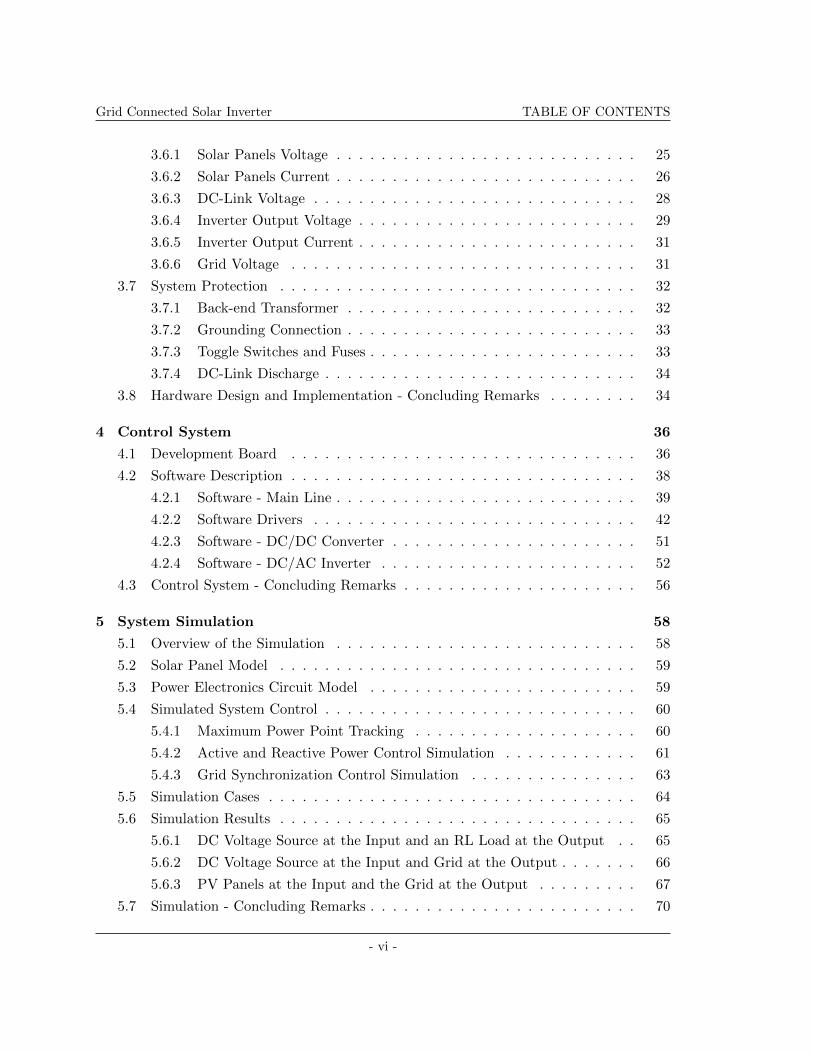
power transistors used in the converter and the inverter. Figure 1.1 shows the overall block
diagram of the system. The DC power produced by the PV panels is first passed through
- 1 -
Grid Connected Solar Inverter
Fig. 1.1: Overall system block diagram
the DC/DC converter, which steps up the panels voltage to the required level at the DC
link. A large DC link capacitor, Clink, provides power decoupling capability and therefore,
reduces fluctuations that may lead to distortion at the output. Next, the DC/AC inverter,
the filter and the 1:2 transformer altogether convert the DC power to AC and synchronize
the phase, the voltage and the frequency with the grid. All measured signals such as
current and voltage of the PV panels and the system output, DC link voltage, and the grid
voltage are processed in the microcontroller. Based on the obtained measurements, the
microcontroller issues two pulse width modulated switching signals: one for the converter
control and one for the inverter control. The signals are passed through the gate drivers
circuitry that provides amplification and isolation between high and low power components
of the system.
This report will first discuss the project specifications in Chapter 2. Next, Chapters 3
and 4 will discuss the development of the hardware and software as individual components.
Chapter 5 will present the created PSCAD simulation cases and their results. The following
chapter will describe in detail the tests that were performed on the entire system and the
consequent troubleshooting. Lastly, Chapter 7 will present the project conclusion.
- 2 -

Grid Connected Solar Inverter 2. Project Specifications
Chapter 2
Project Specifications
The specifications of the project are based on constraints posed by the input and output
of the system. The input comes from a photovoltaic array with maximum ratings of 300W
power and 34V voltage at maximum power point. The output is connected to the electrical
grid, which has a rated voltage of 120Vrms and frequency of 60Hz. Power transfer from
the solar panels to the grid is proportional to the angle difference δ between the inverter
voltage VINV and the system output voltage VSY S , as shown in Figure 2.1
Fig. 2.1: Power flow diagram
The impedance X between the inverter and the grid connection point represents the filter
and the transformer impedances. Equation (2.1) describes the relationship between the real
- 3 -

Grid Connected Solar Inverter
power output P and the power angle.
P =|VINV ||VSY S |
Xsin(δ) (2.1)
Therefore, maximum power is transferred when the power angle is δ = 90, while all other
parameters are constant. To ensure stable system operation during possible disturbances
coming either from the grid or the system, we set the power angle to 30 [1]. Since the
inverter output voltage must be synchronized with the grid, its magnitude must be equal
to the grid voltage divided by two to account for the 1:2 transformer ratio. This results in
VINV = 60Vrms. Now, from Equation (2.1) we can calculate the impedance of the inverter
side inductor X as follows:
300 =60× 60
Xsin(30)
X = 6Ω
The value of X will be used later in the 3.4.1 to calculate the inductance component of the
filter. Moreover, to have the capability of power factor adjustment between 0.8 lagging and
0.8 leading we control the reactive power flow Q according to Equation (2.2).
Q =|VSY S |(|VINV |cos(δ)− VSY S)
X(2.2)
If the desired power factor is unity, we set reactive power to zero in Equation (2.2) and
determine the corresponding maximum inverter voltage as follows:
0 = |Vsys|(|Vinv|cos(δ)− Vsys)
Vinv =Vsyscos(δ)
=60
cos(30)
Vinv = 69.3Vrms ≈ 100Vpeak
- 4 -

Grid Connected Solar Inverter
The above calculation shows that to achieve unity power factor the peak voltage at the
output of the inverter must be 100V. This also means that the DC link voltage VDC has
to be at least 100V. To minimize distortion at the inverter output we set the limit on
VDC fluctuations to be ±5% of the maximum 100V. Additionally, to simplify output filter
design, we set the minimum inverter switching frequency to be (21× 60)Hz [6]. Lastly, the
system was designed to achieve above 80% MPPT efficiency. The summary of the system
specifications is found in Table 2.1.
Table 2.1: Project Specification
Parameter Value or Range
PV panel nominal power 300 W
DC bus voltage 100± 5V
Inverter switching frequency > 1.26kHz
Inverter nominal output power 300 W
Grid voltage[12] 108− 127.2Vrms
Grid frequency[12] 59.5 - 60.5 Hz
Power factor 0.8 lagging - 0.8 leading
MPPT system efficiency > 80%
- 5 -

Grid Connected Solar Inverter 3. Hardware Design and Implementation
Chapter 3
Hardware Design and
Implementation
The hardware portion of the project is comprised of the solar panels, DC/DC converter,
DC/AC inverter, filter, gate driver, sensing circuits and system protection circuits. This
section discusses the significance of each component to the project, their design and build
process and finally, the results of implementing them.
3.1 Solar Panels
The solar panels used in this project were provided by the department of electrical and
computer engineering at the University of Manitoba. The panel model SP75 of Siemens
is rated for 75 W of maximum power, 4.4 A of maximum power point current, and 17 V
of maximum power point voltage. As testing conditions in Winnipeg change quite rapidly
due to unpredictable weather, the values of the voltage and current produced by the model
changes. The most ideal condition to test the SP75 is on a cold sunny winter day. The reason
for such ideality is because of the effect of temperature, angle of incidence and intensity of
light on power production by the solar panel. Lower temperature, perpendicular incidence,
- 6 -

Grid Connected Solar Inverter 3.1 Solar Panels
and direct incidence of light without any disruptions such as clouds, smokes, and/or any
other obstacle result in maximum power produced by the solar panel. The behaviour of the
SP75 model is represented in the form of the I-V curve demonstrated in Figure 3.1.
Fig. 3.1: Solar panel IV curve
The maximum power point tracking (MPPT) of the solar panel is done by maintaining
the voltage and current levels of the solar panel at the knee point of the Figure 3.1. The
MPPT algorithm and its implementation will be further discussed in section 4.2.3. There
are four solar panels available to us for this project and they are arranged in two parallel
strings of two series panels. The arrangement is shown in Figure 3.2.
The panels will have a 470µF capacitor in parallel to ensure no fluctuations in the
power of the panels. The capacitor acts as a bypass capacitor for the source and makes
the voltage sense of the solar panels much more stable. In fact, the voltage sense takes
place across this capacitor and the design of the sense circuitry will be further discussed in
section 3.6. The power produced by the solar panels will be next going through the DC/DC
converter to create the 100 V DC bus line. The design and implementation of the DC/DC
converter is discussed in section 3.2.
- 7 -

Grid Connected Solar Inverter 3.2 DC/DC Converter
Fig. 3.2: Solar panel panels setup
3.2 DC/DC Converter
The DC/DC converter is the hardware platform on which the Maximum Power Point Track-
ing is performed. The input voltage of the DC/DC converter provided by the solar panels is
rated for 34 V at the maximum power point. The output voltage of the DC/DC converter
is specified by the product specifications to be at 100 V. Thereby, the boost configuration
was selected to ensure the stated requirement is met. The schematic of this set up is shown
in the Figure 3.3. The DC/DC converter is controlled by the PWM signal provided by
Fig. 3.3: Solar panels setup
- 8 -

Grid Connected Solar Inverter 3.2 DC/DC Converter
microcontroller. The duty cycle of this signal is adjusted by the control system depending
the output of the MPPT algorithm. This is intended to keep the operating power at its
maximum level. The capacitor and inductor selected for the DC/DC converter design are
selected based on the calculations done using equations (3.1) [6] and (3.2)[6] respectively.
∆VDC
VDC=
D
RCf(3.1)
Imin = IL −VPVDT
L(3.2)
In equation (3.1), the resistive load, Rload, is estimated based on the fact that the output
voltage of the system is 100 V and the system is rated for 300 W. The load value is at the
absolute maximum rating which allows for the conclusion of the fact that equation (3.1)
provides the minimum value of the DC link capacitor. Thereby, the DC link capacitor calcu-
lation resulted in that the capacitor value must be greater than 77.65µF . Such calculation
requires duty cycle, D, as well as the switching frequency. The duty cycle is calculated
using the equation (3.3).
VPV
VDC= 1−D (3.3)
In equation (3.3), VPV represents the input voltage of the DC/DC converter and the VDC
represents the output voltage of the DC/DC converter. The resultant duty cycle that would
yield 100 V DC link voltage is 66%. The DC/DC converter switching frequency is set for
3 kHz and all calculations for the converter are done based on this value. The actual DC
link capacitor used in the implementation phase is 12000µF as the cost of capacitors with
the appropriate ratings was too high and use of existing parts was a necessity.
As shown in equation (3.2), the inductor value for the DC/DC converter was calculated
to be greater than 837µH. Such calculation is done by considering a 66% duty cycle as well
as 3 kHz switching frequency. In a similar situation, as the inductors with ratings needed
for this project are expensive and do not fit within the team budget, existing inductor was
- 9 -

Grid Connected Solar Inverter 3.2 DC/DC Converter
chosen at 1.3mH. An isolated diode, FESF16JT, is used in the implementation stage of
the design as represented in Figure 3.3 by Di. The IGBT, STGF17NC60SD, is used for the
implementation of the DC/DC converter as represented by q in Figure 3.3. The isolated
diode and the IGBT are both physically connected to a heat sink to avoid any overheating
throughout the switching process. Both of these ICs are rated for 16 A or higher to ensure
a smooth transition throughout the execution of the MPPT algorithm.
In order to validate the calculations and design of the DC/DC converter, a test was
conducted which entailed using the variable voltage source from the LabVolt setup and
using a function generator to generate the PWM signal to go through the gate drivers and
then to the IGBT gate. The results of this test are shown in Figure 3.4. The test was
conducted at 50% duty cycle and 1.5 kHz switching frequency. As shown in figure 3.4, on
Fig. 3.4: DC/DC converter test results
the top left, the solar panel string voltage is displayed at 31.13 V while the DC line voltage
is 100.6 V. The input solar panel string current is measured at 20 mA. As shown on the
oscilloscope, the DC line voltage has low noise and a constant DC value with minimal ripple.
These values comply with the design parameters discussed in earlier sections and satisfy
- 10 -

Grid Connected Solar Inverter 3.3 DC/AC Inverter
the original requirement of achieving a 100V DC line voltage based on the rated maximum
power point voltage of 17 V per cell. The solar panel string voltage on this test is lower
than the rated value of 34 V but the maximum power point voltage varies depending on
the surrounding conditions. The fact that the test was successfully conducted by having an
input solar panel voltage in the vicinity of the 34 V value.
The DC/DC converter has been connected with the DC/AC inverter and has success-
fully been connected to the grid. Unfortunately, at the moment, the maximum power point
tracking of the DC/DC converter has not been tested using solar panels. This test is to be
conducted with an RL load prior to the final presentation as well as the full system testing
which includes the connection to the grid. In the next section, the DC/AC inverter design
and implementation will be discussed.
3.3 DC/AC Inverter
The DC/AC inverter stage of the system is responsible for converting the DC power gen-
erated from the solar panels into AC power and transfer it to the electrical grid. We have
selected the topology and the type of switches to be used in the inverter system based on
options that allow high rating versatility and optimum outputs to our system. The design
details and the implementation of the inverter are discussed in this section.
3.3.1 Inverter Topology
An inverter is a power electronic device that changes direct current (DC) signals into al-
ternating current (AC) signals. The most commonly used inverter topology is a full-bridge
or a H-bridge inverter which is built with four switches. The conversion of DC to AC is
achieved by using a switching mechanism that directs current flow through the load in both
the positive and negative directions. As a consequence, a pulse width modulated (PWM)
signal with an amplitude equivalent to the DC input source is generated at the output
- 11 -

Grid Connected Solar Inverter 3.3 DC/AC Inverter
terminals of the inverter. Table 3.1 summarizes the output voltage for different switching
combinations of Figure 3.5(a). A half-bridge topology which is built with only two switches
Table 3.1: Switching
Switches Closed Output Voltage, VINV
S1 & S4 +VDC
S2 & S3 −VDC
S1 & S3 or S2 & S4 0 (open)
S1 & S2 or S3 & S4 ∞ (short)
Fig. 3.5: DC/AC inverter topology
is another option that we considered (Figure 3.5(b)). The output waveform a half-bridge
inverter produces is identical to the PWM signal generated by an H-bridge. This topology,
however, produces more harmonics [6] which is highly undesirable to the system. Harmonics
contributes to additional power losses in the system and to achieve optimum results, they
must be avoided as much as possible. For this reason, the team decided to use the H-bridge
topology to perform the inversion of the DC signals into AC.
3.3.2 Types of Switches Considered
There are two types of switches considered for the H-bridge inverter: Metal-Oxide-Semiconductor
Field-Effect Transistors (MOSFETS) and Insulated-Gate Bipolar Transistors (IGBTs). Ta-
ble 3.2 summarizes the range of frequency, voltage and power ratings for the types of
- 12 -

Grid Connected Solar Inverter 3.3 DC/AC Inverter
applications the MOSFETs and IGBTs are preferred to be used[9]. Based on the values
Table 3.2: IGBT vs MOSFET comparison
ParametersTypes of Switch
MOSFETs IGBTs
Frequency > 200kHz < 20kHz
Voltage < 250V > 1000V
Output Power < 500W > 5000W
outlined in Table 3.2, we decided to use IGBT switches for the inverter since it operates
better for low frequencies compared to the MOSFETs. Moreover, IGBTs can handle higher
voltage and power ratings which allows increased flexibility in the event that we choose to
expand the operational ratings of the system.
3.3.3 Inverter Implementation
Although the single-phase system of the project requires only four switches in the inverter,
the team decided to use a three-phase IGBT module which contains six switches. The deci-
sion was made to accommodate possible testing failures. Figure 3.6 shows the configuration
setup used in testing the inverter functionality. In this setup, a Lab-Volt power supply
module, VIN , was used to provide DC input to the inverter. Through a small resistance,
rs, the DC-link capacitor is charged to VDC and a Rload was connected across the output
terminals of the IGBT module measured VINV . To operate the IGBT switches, a function
generator was used to feed input signals to the gates of the switches. The input square-wave
signals from the function generator was set to 3.3Vpk−pk with an offset of 1.65 V to imi-
tate the signals that the microcontroller provides. Figure 3.7 shows the output waveform
obtained from the testing. The blue signal shows the voltage across the DC-link capacitor,
VDC while the purple signal shows the output voltage across the Rload, VINV . The output
square-wave verifies that the inverter is operating according to theory. That is, the positive
- 13 -

Grid Connected Solar Inverter 3.4 Filter
Fig. 3.6: DC/AC inverter setup
and negative peaks of the output is equal to the DC-link voltage and the average is at zero.
The spikes observed can be eliminated once the filter is connected to the inverter module.
3.4 Filter
Before connection to the grid, sinusoidal signals must contain a total harmonic distortion of
less than 5% [4]. Since the square waveform output of the inverter is rich with harmonics,
a filter was designed to improve the output waveform. The design and implementation of
the filter is discussed in this section.
3.4.1 Filter Design
The main responsibility of the filter is to improve the square wave output of the inverter
into a sinusoidal waveform that is suitable for connection to the grid. The simplest low-
pass filter the team designed is that of an L filter that is connected directly to the inverters
output terminals. As well, an LCL filter was designed to further eliminate harmonics of
- 14 -

Grid Connected Solar Inverter 3.4 Filter
Fig. 3.7: DC/AC inverter output test
the square wave output. Figure 3.8 shows the topologies of the the two designed filters.
The topology on the left shows the basic L1 filter placed in between the inverter and the
grid. The topology on the right shows four filter components: the same inductance L1 was
placed on the inverter side while a second inductance, L2, was placed on the grid side. At
the junction of the two inductances, a damping resistor, Rd, and a filter capacitor,Cf , was
connected in series.
Fig. 3.8: Output filters that were considered
- 15 -

Grid Connected Solar Inverter 3.4 Filter
3.4.1.1 L filter calculations
L1 was calculated from the impedance, X (see section 2) using equation (2.1). X = ωL1 =
2πL1f where f = 60Hz. It follows that,
L1 =X
2π60= 15.9mH (3.4)
3.4.1.2 LCL filter calculations
For the second topology, limitations had to be taken into account in choosing the cut-off
frequency, fres of the filter. fres was chosen to be 10 times greater than grid frequency (60
Hz) at the least, and one half of the converter switching frequency at the most [filter ref].
For this reason, we have chosen fres = 610 which is within the given range. The cut-off
frequency is given by Equation (3.5).
fres =1
2π
√L1 + L2
L1L2Cf(3.5)
Cf was set to 47µF and by performing algebraic manipulation on Equation (3.5), we can
calculate L2. Moreover, Rd is given by Equation (3.6) [5] and was calculated as follows:
Rd =1
3ωresCf= 1.84Ω (3.6)
Since the back-end transformer is connected to the filter, we had to account for its
leakage inductance in finalizing the value of L2. Therefore, we performed open and short
circuit tests on the transformer to find its reactance parameters.
In performing the open circuit test (OCT), we left the secondary side open-circuited,
applied the rated voltage at the primary side then measured the voltage, current and power
on the LV side. On the other hand, in performing the short circuit test (SCT), we short-
circuited the primary side, applied the rated current on the secondary side then measured
- 16 -

Grid Connected Solar Inverter 3.4 Filter
the voltage, current and power on the HV side. Table 3.3 summarizes the values obtained in
OCT and SCT. Using Equations (3.7) and (3.8), the approximation model of the transformer
reactance shown in Figure 3.9 was derived.
Table 3.3: OCT and SCT results
Tests Voltage Current Power
OCT 109.70 V 0.174 A 7.25 W
SCT 14.77 V 2.307 A 34.02 W
Xoc =Voc
Iocsinφ
Roc =Voc
Ioccosφ
(3.7)
where φ = cos−1(Poc
VocIoc)
Rsc =Psc
I2sc
Xoc =
√(VscIsc
)2 +R2sc
(3.8)
Since the current that goes through the shunt branch is negligible compared to the current
Fig. 3.9: Transformer model
that goes to the main line through the series impedance[ref], Xoc and Roc were not consid-
ered in calculating the final value of L2. Therefore, L2 = L2,old−Lsc where L2,old = 1.6mH
- 17 -

Grid Connected Solar Inverter 3.4 Filter
as previously calculated in Equation (3.5) and Lsc =Xsc
ω. The final values of the designed
filter components can be found in Table 3.4.
3.4.2 Filter Implementation
The functionality of the filter was tested by integrating it at the output terminals of the
inverter. Two tests were performed in total to confirm our designed filters. The filter test
setup and methodology are shown in Figure 3.10.
Fig. 3.10: Filter implementation setup
3.4.2.1 L Filter
Typically, an SPWM signal should be fed to the gates of the IGBTs in order to generate
a sinusoidal output. However, the main objective of the initial test with the L filter was
to confirm the hardware operation as oppose to software, hence, a function generator was
sufficient to provide the input.
Due to budget constraints, we were not able to acquire the 1.6 mH inductor that
we calculated in our design. We used a 20.6 mH inductor instead since this is the closest
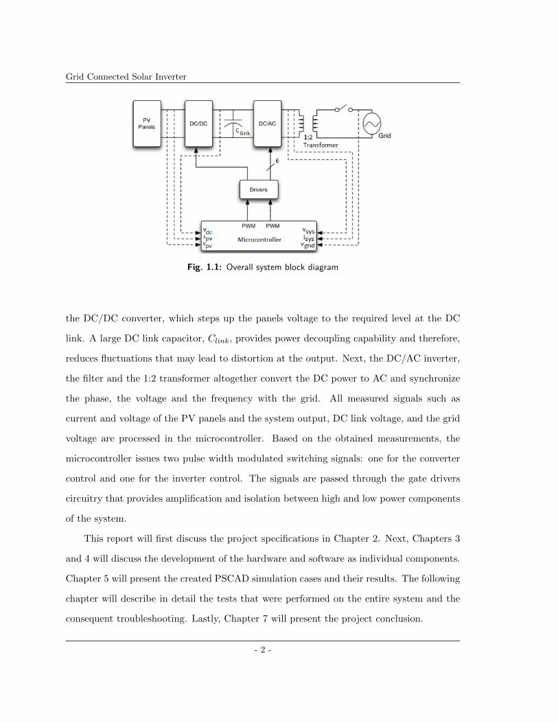
inductance value that is available in the department. Figure 3.11 shows the output obtained
using the L filter. In comparison to the VINV result obtained in section 3.3.3, it is evident
- 18 -
Grid Connected Solar Inverter 3.4 Filter
that the waveform in yellow which is the voltage after the filter, VOUT is much smoother.
However, it is still not close to the desired sinusoidal output. Although the unsatisfactory
result in this test was expected since actual SPWM input signals were not used from the
microcontroller, the team decided to improve the filter.
Fig. 3.11: L filter test result
3.4.2.2 LCL Filter
An LCL filter was next integrated to the inverter module. For this test, the function gener-
ator input was replaced with SPWM input from the microcontroller. Again, due to budget
constraints and the availability of the components in the department, the actual values used
in the filter is not exactly the same as the values obtained in the design calculations. Table
3.4 summarizes the filter designed and actual component values used in the project. When
the LCL filter was integrated with the inverter, we obtained results shown in Figure 3.12
was obtained. It was apparent that a much more improved sine wave VOUT was generated
at the output terminals of the inverter. This verified that unwanted higher frequency com-
- 19 -

Grid Connected Solar Inverter 3.4 Filter
Table 3.4: Designed and actual filter components
Filter parts Design values Actual values
L1 15.9 mH 20.6 mH
L2 1.6 mH 1.5 mH
Cf 47µF 60µF
Rd 1.84Ω 2Ω
ponents were successfully filtered out. However, it is also apparent that there was a large
voltage drop from the DC-bus voltage to the output. The issue was later resolved by adding
more delay to the switching signals, which will be discussed further in section 3.5.
Fig. 3.12: LCL filter test results
- 20 -
Grid Connected Solar Inverter 3.5 Gate Drivers
3.5 Gate Drivers
3.5.1 Gate Drivers Theory
The function of the gate driver circuit is to provide isolation and protection for the mi-
crocontroller from the high voltage components. The circuit also amplifies the signals the
microcontroller sends to control the DC/DC converter and the DC/AC inverter. Figure 1.1
shows a block diagram of the entire system including the location of the gate driver circuit.
The driver system is connected to the microcontroller, the DC/DC converter, and DC/AC
inverter.
The driver circuit takes in a 3.3 V input from the microcontroller and outputs the
required gate voltage of 12V at a higher current to switch the gates of the DC/DC converter
and DC/AC inverter. For the DC/DC converter, the duty cycle of the signal is used to
control the output voltage. The gate driver system amplifies and outputs the duty cycle
signal. For the DC/AC inverter, there are four gates in a H-bridge design. This requires
four separate outputs from the single input of the microcontroller. The input is a SPWM
signal used to convert from DC to AC. Two gates must be on while the other two are off
for the DC/AC inverter. Therefore, the signal has to have an inverted and non-inverted
component created from the single input. Applying a voltage to the H-bridge design also
introduces a problem for the gate drivers as the gate closest to the DC bus called the high
side gate has its emitter at a floating voltage. An exterior circuit was designed to solve this
problem and is discussed in the next section.
3.5.2 Gate Drivers Schematic
The final block diagram of the design for the driver system is shown in Figure 3.13. It
contains the buffer, not gate, XOR gate, one-shot, optocouplers labelled as optos, gate
driver IC’s and shows how the ICs are connected. The output from the top two drivers
- 21 -

Grid Connected Solar Inverter 3.5 Gate Drivers
Fig. 3.13: Gate drivers schematic
control the DC/AC inverter, while the bottom driver controls the DC/DC converter. The
figure does not include the extra components required around each of the ICs such as the
bootstrap circuit or the bypass capacitor. The entire circuit was rebuilt on a development
board that fits onto the microcontroller tower. The schematic itself is the same but it is
more compact, eliminating the need for a project board. It also would eliminate noise due
to long wires on the project board.
3.5.3 Gate Drivers Implementation
The gate driver system was built and tested on a project board. This provided easy access
to 5V and 12V needed for the circuit. It also provided a ground for the neutral of the
H-bridge. Testing was done using the project board with input from the microcontroller as
well as a signal generator. To test the circuit functionality the output waveform of both
the DC/DC driver output as well as the DC/AC driver were measured. Also, the undesired
delay the circuit introduces and the delay that is meant to be introduced for the DC/AC
inverter were also measured to ensure the timing of the signals was adequate.
The DC/DC driver has one output that changes with the duty cycle of the input
signal. Figure 3.14 shows the output from the DC/DC converter’s driver at two different
- 22 -

Grid Connected Solar Inverter 3.5 Gate Drivers
duty cycles. The input is a square waveform from the microcontroller with 0 V when low
Fig. 3.14: 72% duty cycle output and 22% duty cycle output to DC/DC
and 3.3 V when high. The output voltage of the driver is 0 V when low and 11.4 V when
high. There is a drop in voltage from the 12V supply but it is still above the gate threshold
required for switching. The output is matching the input signal but is amplified. This
is the required and expected result showing that the DC/DC driver output is functioning
correctly. The DC/AC driver output is more complex than the DC/DC driver as it has
four outputs coming from one signal. Two of the signals are high at once while the other
two are low so only the measurement of two of the signals is shown even though all were
tested. The test was performed using the signal generator before it was connected to the
microcontroller to ensure it would not cause any damage. Figure 3.15 shows the output
of the DC/AC driver. Figure 3.15 shows that the output of one signal is high while the
other is low. The output voltage is 12V which is larger than the threshold value. This result
meets the requirements for driving the inverter. After observing the output of the sine wave
from the inverter, a delay circuit was introduced to the driver system to remove the spikes
that were seen in the signal. This would stop any chances of a short circuit being created
in the inverter if both signals were on for a small amount of time. Figure 3.16 shows the
measured delay that was introduced using the one shot and XOR gate circuits. In Figure
3.16, the input is the red line while the output is the blue line. The figure shows that the
- 23 -

Grid Connected Solar Inverter 3.5 Gate Drivers
Fig. 3.15: Inverted and non-inverted signals to DC/AC inverter
Fig. 3.16: Delay from XOR and One-shot measurement
delay is approximately 2.5µs from when the input goes high to when the output goes high.
This delay is enough to stop any chances of a short circuit occurring as the largest overlap
that we saw was less than the delay that was introduced. Unfortunately after testing the
inverter again the sine wave still had spikes. This leads us to believe that the spikes may
not be caused by a short circuit in the H-bridge. The last test result for the gate drivers
is measuring the delay introduced by the ICs from the input to the output. This delay is
caused by the propagation delay through the ICs. This delay had to be small enough to be
negligible at the switching speed we are using. Figure 3.17 shows the measured delay.
- 24 -

Grid Connected Solar Inverter 3.6 Sensing Circuits
Fig. 3.17: Propagation delay of gate driver circuit
3.6 Sensing Circuits
In order to generate the switching signals to operate the IGBTs of the converter and the
inverter, the microcontroller needs signal inputs from the solar panels, DC-link capacitor,
inverter output and the grid. These signals, however, cannot be fed directly to the micro-
controller since their ratings are much higher than what the microcontroller could handle.
Therefore, measuring or sensing circuits were designed to attenuate the signals into levels (0
to 3.3 V) suitable for the microcontroller. The design and implementation of such sensing
circuits are discussed in this section.
3.6.1 Solar Panels Voltage
The purpose of voltage measurement of the solar panel strings is to provide the MPPT
algorithm with its input voltage. In order to accomplish such measurements, two different
designs were considered. The first design entailed a resistor divider which divides 40V input
to 3.3V to enter the microcontroller as an input. The 3.3V level is protected by clamping
diodes to avoid damaging the microcontroller due to overvoltage. The clamped divider
design requires an earth ground which creates issues for the H-bridge set-up of the DC/AC
- 25 -

Grid Connected Solar Inverter 3.6 Sensing Circuits
inverter. The second method follows the same methodology of using a resistor divider to
be able to measure the voltage within the 0-3.3V range of the microcontroller pin. The
only exception is that it uses an isolation amplifier to isolate the microcontroller from the
grid and the solar panels. In this case, there is no earth ground connection needed in the
sensing circuitry which ensures that the DC/AC inverter operation will happen without
any issues. The isolation voltage sense circuitry is done by using the appropriate resistor
divider and the isolation amplifier AD202JY. Testing of such design has been done with the
microcontroller. Equation (3.9) shows the relationship between the sensed voltage of the
solar panels VPV and the voltage read by the microcontroller input voltage level.
VPV = 14.39676269Vmicro2 (3.9)
The second design option is the final design as it integrates with the system without any
problems in regards to the grounding. Solar panel current sense circuitry will be discussed
in the next section.
3.6.2 Solar Panels Current
The purpose of solar panels’ current measurement is to provide the current value for the
maximum power point tracking algorithm perform by the microcontroller. Such measure-
ment has to be done so that there is an isolation between the line current and the micro-
controller. Thereby, hall-effect sensor ACS712 is used to measure the current. The ACS712
provides a linear output voltage of 100 mV per 1 A of current sensed. As our system is
designed for a 8.8 A maximum power point current, the output voltage range provide by
the IC is 880 mV which spans from 2.5 V to 3.38 V. Therefore, as a result, the microcon-
troller would have low precision on its current sense values from the solar panels hence a
low quality tracking by the algorithm. Such dilemma was solved by designing a differential
amplifier that was placed in between the hall-effect sensor and the microcontroller to ensure
- 26 -

Grid Connected Solar Inverter 3.6 Sensing Circuits
the range of 0 - 2.6 V. The schematic of the current sense circuitry is shown in the below
Figure 3.18. The hall-effect current sense circuitry was implemented and tested using vari-
Fig. 3.18: Schematic of the hall-effect current sense circuitry
able current source supplied by the LabVolt set up at the Manitoba Hydro Power Systems
Research Suite at University of Manitoba as well as the solar panel modules SP75. The
results of the tests are shown in the below graph. The current provided by the LabVolt
source was measured by the current sensor on the LabVolt setup as well as multimeters to
avoid any noise on readings displayed on the LabVolt software. The equation of the line
of best fit was an accurate way of formulating values by the microcontroller because of the
natural linearity of the output voltage from ACS712. The equation that was extracted from
the Figure 3.19 is viewed by the software as a voltage between 0 V - 2.5 V which resembles
current sensing of 0 A - 8.8 A. Equation (3.10) describes this relationship.
IPV = 7.860778883− 3.159477Vmicro1 (3.10)
In the next section, the DC-link Voltage sense circuitry design and implementation is dis-
cussed.
- 27 -

Grid Connected Solar Inverter 3.6 Sensing Circuits
Fig. 3.19: Test results of the hall-effect current sensing
3.6.3 DC-Link Voltage
There are three main reasons for measuring the voltage across the dc-link capacitor. First,
at start-up of the system, we need a means of knowing whether the dc-link capacitor has
been pre-charged to the desired value. Second, when system is turned off, it is necessary
to make sure that the capacitor is discharged to 0 V for safety reasons. And lastly, during
operation, the voltage fluctuation on the DC-bus needs to be measured as this is required
for generating the control signals of the inverter. These three points will be discussed in
more detail in the simulation and software sections.
We decided to use an isolation amplifier for measuring the dc-link voltage. As the name
suggests, the device was chosen because it provides isolation between the power electronic
circuit and the microcontroller. As shown in Figure 3.20, the amplifier was connected across
the smaller resistance, R2, of the resistive divider that is connected in shunt to the capacitor.
We chose R1 to be a high resistance, 120kΩ, to ensure that most of the current will go to the
inverter instead of the shunt branch. And since 120 V is the absolute maximum voltage that
we may get from the dc-link as will be discussed in our simulation case, we chose R2 such
that for this input voltage, 3.3V is generated at the output of the isolation amplifier. 3.3
- 28 -

Grid Connected Solar Inverter 3.6 Sensing Circuits
Fig. 3.20: Isolation amplifier connection for measuring VDC
V is the maximum voltage the microcontroller could handle, therefore the design decision
allows us to achieve a good resolution. Equation (3.11) gives the relationship derived as a
result of performing voltage division to R1 and R2, where vdc is the attenuated signal of
VDC .
VDC =R1 +R2
R2vdc
=120kΩ + 3.3kΩ
3.3kΩvdc
= 37.36vdc
(3.11)
3.6.4 Inverter Output Voltage
The purpose of measuring the inverter output voltage is to track its phase and amplitude
which are both necessary for SPWM generation. Since the low and high power circuitry
require isolation, we decided to use a potential transformer with a turns ratio of 110:3 to
step down the voltage. In addition, since the microcontroller input requirements does not
allow negative measurements, we designed, built and tested an op-amp based offset circuit
that is connected on the secondary side of the potential transformer. This circuit introduces
a dc-offset to the attenuated signal of the inverter output as shown in Figure 3.21. Using
- 29 -

Grid Connected Solar Inverter 3.6 Sensing Circuits
Fig. 3.21: Op-amp based offset circuit
nodal analysis at the non-inverting input of the op-amp, Equation (3.12) was derived:
vo = αVSIG + VOFFSET (3.12)
where α = RaRbR2Rb+RaR2+RaRb
. After performing further analysis, the following resistor values
were selected: R1 = 1.0kΩ, R2 = 2.8kΩ, Ra = 33kΩ and Rb = 3.9kΩ. Ra and Rb were
chosen such that the offset is approximately half of the full range of the microcontroller
input. That is, VOFFSET ≈ 1.65. R2 was chosen based on the estimated ac voltage range
of 0 to 60 Vrms we expect at the inverter output. R1 functions as a feedback connection
between the output and the inverting input of the op-amp. Moreover, a 10µF coupling
capacitor was connected in series with R2 to make sure that only the AC signal from the
input goes to the circuit. Equation (3.13) gives the final ratio used by the microcontroller
to evaluate the output voltage of the inverter, where vsys,pk is the attenuated VSY S,pk with
offset.
VSY S,pk =vsys,pk − VOFFSET
α
(110
3
)=vsys,pk − 1.44
0.56
(110
3
) (3.13)
- 30 -

Grid Connected Solar Inverter 3.6 Sensing Circuits
3.6.5 Inverter Output Current
Similar to the purpose of the inverter output voltage sensing circuit, the inverter output
current needs to be measured since its phase and amplitude are both necessary for SPWM
generation. We decided to use a Hall Effect current transformer to measure the output
current since this device provides isolation as well as the flexibility of choosing by how
much we could attenuate the current signals. The ratio of attenuation can be adjusted by
varying the number of turns in the current transformer.
Using the schematic shown in Figure 3.21 and the general formula given in Equation
(3.12), we chose the resistors for the dc-offset circuit that will give the best resolution
for measuring the estimated current range of 0 A to 5 A that we expect at the inverter
output. Moreover, we have tried several number of turns ratio to the current transformer
and our tests have shown that a number of 5 turns gives us the desired full range that we
want without exceeding the microcontroller input requirements. As a result, the following
resistor values were selected: R1 = 1.0kΩ, R2 = 3.3kΩ, Ra = 33kΩ and Rb = 3.9kΩ.
Equation (3.14) gives the final ratio used by the microcontroller to evaluate the output
current of the inverter, where isys,pk is the attenuated ISY S,PK with offset.
ISY S,pk =isys,pk − VOFFSET
α
(10
no.ofturns
)=isys,pk − 1.52
0.51
(10
5
)= (isys,pk − 1.52)× 3.89
(3.14)
3.6.6 Grid Voltage
The main purpose of measuring the grid voltage is to track its frequency in order for the
microcontroller to synchronize the sinusoidal signal we produce at the output of the inverter
to the grid. In designing the sensing circuit for the grid voltage, the same process was taken
as described in section 3.6.4. That is, a 110:3 potential transformer was also used and the
- 31 -

Grid Connected Solar Inverter 3.7 System Protection
same schematic in Figure 3.21 for the dc-offset circuit was implemented. Moreover, Ra, Rb
and R1 were chosen for the same reasons as discussed earlier. The only difference is the
selection of R2 which was chosen based on the estimated grid voltage range of 0 to 120Vrms.
As a result, the following resistor values were selected: R1 = 1.0kΩ, R2 = 8.9kΩ, Ra = 33kΩ
and Rb = 3.9kΩ. Equation (3.15) gives the final ratio used by the microcontroller to track
the grid voltage, where vgrid,pk is the attenuated VGRID,PK with offset.
VGRID,pk =vgrid,pk − VOFFSET
α
(110
3
)=vgrid,pk − 1.52
0.28
(110
3
)= (vgrid,pk − 1.52)× 130.95
(3.15)
3.7 System Protection
Apart from the main hardware components that have already been discussed in this report,
additional components were designed and/or implemented to the system to provide protec-
tion. Most of these components are not necessarily required for system operation; however,
they are extremely important to prevent potential damage and harm to the hardware com-
ponents as well as to the persons handling and operating the system. The protection circuits
implemented are discussed as follows.
3.7.1 Back-end Transformer
The transformer that is placed in between the filter and the grid serves as the main mecha-
nism that isolates the system to the grid. The isolation provides protection to the hardware
components as well as the grid in the case that faults arise on either side of the transformer.
Moreover, we took advantage of the component by acquiring a transformer that has a
turns ratio of 1:2. This allowed us to design our system for half of the grid voltage; and
more importantly, we were able to build the system with lower rated components that are
- 32 -

Grid Connected Solar Inverter 3.7 System Protection
much cheaper.
3.7.2 Grounding Connection
Determining the ground connection of the hardware components is a crucial concern that
needs to be considered for proper system operation. If the grounding connections are not
assembled correctly, the purpose of using parts that provide isolation between the high
and low power rating components of the system is defeated. Moreover, the system would
generate erroneous output signals. Figure 6.1 shows the grounding connection we used for
each hardware component. Notice that the high power electronic circuitry and a portion
of the gate driver are referenced to a floating ground. The floating ground is the same
as the reference of the +12 V supply auxiliary supply we used to power the IC chips of
the gate driver. On the other hand, the microcontroller and a portion of the gate driver
is referenced to earth ground. The gate driver reference grounds was discussed in section
3.5.3. These grounding connections were implemented in performing the overall system
testing and troubleshooting of the project.
3.7.3 Toggle Switches and Fuses
Six sets of switches in series with fuses are implemented to the system. One pair is placed
in the high and low sides in between the solar panels and the DC/DC converter. Another
pair is placed in between the dc-link capacitor and the inverter, and finally, the third pair is
placed in between the secondary side of the 1:2 transformer and the grid. This protection
mechanism enables the system to break connections when unexpected high currents occur.
The switches we used are all manually-operated; however, it is the microcontroller that
dictates the opening and closing of these switches. When certain conditions are met, the
microcontroller will light a LED which signifies that the concerned hardware components
are ready to be connected or have to be disconnected. These conditions will be further
- 33 -

Grid Connected Solar Inverter 3.8 Hardware Design and Implementation - Concluding Remarks
discussed in the software section.
3.7.4 DC-Link Discharge
The DC-link capacitor is expected to hold a voltage up to 100 V. For safety reasons, the
capacitor needs to be discharged to 0 V when the system is turned off. Therefore, a simple
discharging circuit was designed and connected across the DC-link capacitor.
The circuit is made up of a low resistor, 75Ω and a toggle switch connected in series
to ground. During system operation, the switch is opened so as to avoid prematurely
discharging the capacitor. After system operation, the switch is closed which connects the
high side of the capacitor through the resistor to ground. It takes 5 time constants to fully
discharge a capacitor, therefore with a Clink = 12000µF, we expect the capacitor to be
discharged for no greater than 5τ = 5RC = 0.45 seconds.
3.8 Hardware Design and Implementation - Concluding Re-
marks
The hardware portion of the project is comprised of multiple subsystems that includes
the DC/DC converter, DC/AC inverter, filter, gate driver, sensing circuits and system
protection circuits. Each component underwent several design iterations and testing; the
following points summarize the accomplishments of each hardware component of the system:
The DC/DC converter stage of the system was able to boost the solar panel voltage
to the desired VDC of 100V.
The DC/AC inverter stage of the system has successfully produced the desired PWM
output voltage with amplitude equivalent to VDC which confirms that DC input was
converted into AC.
- 34 -

Grid Connected Solar Inverter 3.8 Hardware Design and Implementation - Concluding Remarks
The filter was able to reduce the unwanted frequency components of the square wave
from the inverter as demonstrated by the smooth sinusoidal waveform obtained at the
output of the filter.
All sensing circuitry testing results have shown that all necessary signals for power
electronic control were successfully attenuated into levels suitable to the microcon-
troller as intended.
The protection circuits were implemented to provide overall hardware and user safety.
Overall, individual sections performed as expected and each subsystem met the required
specifications set at the beginning of the project. A list of parts ordered and their costs can
be found in table X of Appendix X. The design calculation results were used as the starting
point for the values used in the simulation of the overall system.
- 35 -

Grid Connected Solar Inverter 4. Control System
Chapter 4
Control System
The control system is responsible for controlling the hardware of the DC/DC converter
and the DC/AC inverter. The following subsection discuss the two main parts of the
system. The first part consists of hardware components such as the development board,
the microcontroller and external peripherals.The second part consists of the software that
runs on the microcontroller.
4.1 Development Board
The development board that was chosen for this project is the tower module TWR-56F8400
form Freescale.[13] This particular development board is populated with an MC56F84789
digital signal controller. Additionally, the board came with Freescale‘s CodeWarrior De-
velopment Studio which is an integrated development environment (IDE). Besides debug
interface, there are many benefits when it comes to CodeWarrior Development Studio, es-
pecially the processor expert interface. This interface provided us with friendly controls in
order to automatically generate the required initialization routines for the microcontroller
peripherals. Yet another benefit of the chosen development board is its modularity. The
tower development system allows to connect up to 4 tower modules in between the eleva-
- 36 -

Grid Connected Solar Inverter 4.1 Development Board
tor modules. Figure 4.1 shows how the low voltage circuits of the system are assembled
together.
Fig. 4.1: Assembled tower system
Figure 4.2 demonstrates how the microcontroller pins are connected, both internally and
externally. Additionally, the figure also shows that the MC56F84789 controller is equipped
with all of the peripherals that the inverter requires with the exceptions of three comparators
and one digital to analog convertor (DAC). The need for this additional peripherals is due
to deviations from the original software design. Initially, the sinusoidal and the triangular
waves were virtual signals residing in the software, thus eliminating the need for the external
DAC. Additionally, both signals were compared in the software as well, enabling the use
of the eight channel modulated comparator. However, in later stages of the development,
it became clear that it is inefficient to perform the comparison in software. Therefore,
the built in comparator was utilized in order to perform the continuous comparison of a
- 37 -

Grid Connected Solar Inverter 4.2 Software Description
triangular wave generated by the built in DAC, and the sinusoidal wave generated by an
external DAC.
Fig. 4.2: MC56F84789 microcontroller internal and external connections
4.2 Software Description
This section describes the software that controls the grid-tie inverter system. The software
development approach that was chosen for this project is the divide and conquer method.
- 38 -

Grid Connected Solar Inverter 4.2 Software Description
The main benefit of this approach is the ability to separately develop and test smaller
software modules without the need to wait for the entire program to function. An additional
benefit of the divide and conquer method with regards to the software development, is the
ability to test hardware subcircuits as soon as they are available. The software application
implements a combination of interrupt driven routines along with a state machine running
in the background. The entire program was divided into four main submodules: Main
Line, Drivers, DC/DC Software, and DC/AC Software. The following subsections provide
detailed analysis of each of the submodules.
4.2.1 Software - Main Line
Upon startup/reset of the inverter, the main-line code is the first one to run. This software
is responsible to ensure safe initialization of the entire system. After system initialization is
complete, the main-line software enters an endless loop which implements a state machine
that periodically runs different background tasks. Figure X illustrates the main-line software
flow chart which includes the following states.
Initialization state: Runs when the system is turned ON or Reset. In this state the
program calls different initialization routines in order to initialize peripherals, drivers
and global variables. The system then moves to the precondition state.
Precondition state: Ensures that the input signal from both the PV panels and the
Grid are valid. The passing conditions for the PV panels output are minimum power
and voltage values of 30W and 24V respectively. Additionally, the grid signal must
have frequency of 60± 0.5Hz. If the any of the preconditions are violated the system
moves into error/standby state. Otherwise the system moves to precharge DC link
capacitor state.
Precharge state: Starts the DC/DC precharge operation by issuing the DC/DC PWM
- 39 -

Grid Connected Solar Inverter 4.2 Software Description
signal with 50% duty cycle. Next, the software measures the voltage across the capac-
itor every 100µs and if a measurement of 100V or above is received the system starts
the DC/AC operation and enters the main loop state. Additionally, a one minute
timeout counter is activated from the moment the PWM signal is issued. In case the
voltage across the DC link capacitor does not reach 100V within the allowed minute,
the system moves to error / standby state.
Error / standby state: Turns off the system and waits for 10 minutes before moving
to the precondition state.
Main loop: Infinite loop which includes 5 states: invariants checking, MPPT, grid
sync, amplitude PI, and phase PI. The main loop responsibility is to periodically fire
up the currently pending state. Figure X demonstrates the main loop flow chart with
the following states:
Invariants state: Fires up every 50ms. Responsible to enforce the same condi-
tions as the precondition state enforces. Additionally, since the inverter is now
fully functional, the invariants state is also responsible to ensure valid output
from the inverter itself. A valid output signal from the inverter must have the
same frequency as the grid signal with maximum error of 0.2Hz. If any of the
invariants are violated the system moves into error / standby state. Otherwise
the state exits to the main loop.
MPPT state: Fires up every 500ms. Calls the DC/DC software in order to
execute the MPPT algorithm. Refer to section Software - DC/DC converter for
more details.
Grid sync state: Fires up every 100ms. Calls the DC/AC software in order to
synchronize the inverter output to the grid. Refer to section Software - DC/AC
inverter for more details.
- 40 -

Grid Connected Solar Inverter 4.2 Software Description
Amplitude PI state: Fires up every 250ms. Calls the DC/AC software in order
to run the PI Controller that controls the modulation index of the SPWM signal.
Refer to section Software - DC/AC inverter for more details.
Phase PI state: Fires up every 250ms. Calls the DC/AC software in order to run
the PI Controller that controls the phase of the SPWM signal. Refer to section
Software - DC/AC inverter for more details.
- 41 -
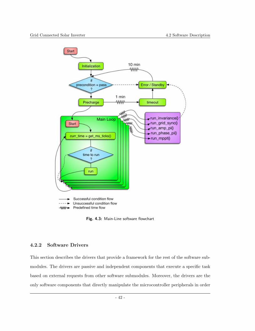
Grid Connected Solar Inverter 4.2 Software Description
Fig. 4.3: Main-Line software flowchart
4.2.2 Software Drivers
This section describes the drivers that provide a framework for the rest of the software sub-
modules. The drivers are passive and independent components that execute a specific task
based on external requests from other software submodules. Moreover, the drivers are the
only software components that directly manipulate the microcontroller peripherals in order
- 42 -
Grid Connected Solar Inverter 4.2 Software Description
to perform the required function. Therefore, the main-line software calls the initialization
methods provided by the drivers in order to initializes the microcontroller peripherals. The
following subsection provide additional details for each of the four main drivers.
4.2.2.1 Frequency Driver
The frequency driver is used to measure the frequency of a square wave signal. This driver
is implemented 3 times in order to measure the frequency of inverter voltage and current
signals and the grid voltage signal. The initialization routine provided by driver initializes
a 16 bit timer to increment every 1µs. It does that by setting the timer to increment on
both rising and falling edges and then supplies 2µs frequency signal (50% duty cycle) to
the input pin of the timer. Next, the interrupt pin, associated with the input signal that
need to be measured, is set to interrupt on rising edges. Finally, the routine enables both
the counter and the interrupt pin.
After initialization is complete, the driver is constantly measuring the frequency of the
input square wave. Figure 4.4, represents the flow chart of the interrupt service routine
(ISR) that gets called on every rising edge of the input square wave. The ISR computes
the period of the signal by averaging it over the last 10 valid periods. A valid period is one
that differs from the last valid period by no more than 10µs (at 60Hz, 10µs correspond to
0.036Hz). As soon as 10 valid periods are measured, the average frequency can be obtained
from the reciprocal of the period. Finally the ISR resets and a new measurement can be
computed.[10]
- 43 -

Grid Connected Solar Inverter 4.2 Software Description
Fig. 4.4: Flowchart for frequency measurement ISR
4.2.2.2 Voltage driver
The voltage driver is used to measure voltage values that are connected to the ADC periph-
eral of the microcontroller. The driver’s initialization routine sets up three ADC channels
in order to measure the PV voltage, current values and the DC link voltage. Additionally,
the driver initializes an internal interrupt to fire up every 10ms. This interrupt is used in
order to start the ADC conversion. The driver functioned as required during a dummy test
that used the output of a function generator as an input to the ADC. Additionally, since
the ADC has an accuracy of 12 bits, the corresponding voltage accuracy is 0.806mV and
- 44 -

Grid Connected Solar Inverter 4.2 Software Description
can be calculated as follows:
Q =3.3V
212=
3.3V
4096= 0.806mV (4.1)
4.2.2.3 Triangular Wave Generation Driver
The triangular wave driver uses the build-in 12 bit DAC automatic waveform generation.
In order to initialize the DAC the following information must be calculated:
Range of the triangular wave (maximum - minimum)
Step size between each DAC update
Update rate that forces the DAC to change its value by the step size
Our objective is to generate a triangular wave with frequency of 1.26kHz and voltage sweep
that uses the entire voltage range of the DAC. Therefore, we first calculate the quantization
step Q of the DAC. Since the DAC’s reference voltage is 3.3V with 12 bit accuracy, Q
is given by Equation (4.1). The range of the triangular waveform is 3.3V (DEC: 4095,
HEX: 0xFFF) and the required frequency is 1.26kHz (0.794ms). Additionally, the DAC’s
maximum settling time is 2µs thus the maximum number of updates in 0.794ms is given by
Equation (4.2):
DACupdates =794
2= 397 (4.2)
Next we calculate the step size corresponding the the maximum number of updates:
DACstep =Range
Updates=
4095
397= 10.31 (4.3)
The step size is rounded up to 11 and a new update count is calculated:
DACupdates =4095
11= 372.36 (4.4)
- 45 -

Grid Connected Solar Inverter 4.2 Software Description
Finally the DAC’s update rate can be obtained from Equation (4.5):
DACUpdateRate = 2(372.36updates
0.794ms) = 937.943kHz (4.5)
The driver test achieved the required results and Figure 4.5 shows the triangular waveform
generated by the built-in DAC.
Fig. 4.5: Triangular waveform
4.2.2.4 Sinusoidal Wave Generation Driver
The sinusoidal wave generation driver is responsible for generating a sinusoidal waveform
with specific frequency and amplitude. The driver uses the external DAC5863 in order to
generate the sinusoidal waveform. In addition, the driver utilizes Freescale’s off the shelf
assembly library, 56800E, in order to generate the sinusoidal lookup table. [3] Figure 4.6
shows the software flow chart that initializes and modifies the two lookup tables. Each
table includes 360 values that correspond to 360 degrees of the sinusoidal waveform. Since
the GFLIBSinT lr() function, provided by Freescale, is expensive in terms of execution
time, the driver alternates between the two lookup. By switching to the updated lookup
table only when it is ready, the driver ensures smooth amplitude transition in the generated
- 46 -

Grid Connected Solar Inverter 4.2 Software Description
sinusoidal waveform.
Fig. 4.6: Flowchart for sinusoidal lookup table generation
In addition to the amplitude adjustments, the driver also enables frequency and phase
synchronization. The driver provides four methods that allow external software to increment
or decrement the phase shift and the frequency of the waveform. Figure 4.7 demonstrates
the interrupt service routine (ISR) which is responsible for updating the external DAC’s
output voltage. The ISR keeps record of the current phase of the sinusoidal waveform as well
as the requested phase shift. Upon firing up the interrupt, the ISR retrieves the sinusoidal
voltage value that correspond to the current degree. It then outputs the retrieved value
through the 12 output pins that are used to interface with the external DAC. Finally it
- 47 -

Grid Connected Solar Inverter 4.2 Software Description
prepares the next degree that will be retrieved in the following interrupt. [11]
Fig. 4.7: Flowchart for sinusoidal update ISR
The driver was tested by synchronizing it to an attenuated grid signal. Figures 4.8,
4.9, 4.10, and 4.11 show test results of the driver. The blue signal represents the gener-
ated sinusoidal waveform and the red one represents the attenuated grid signal. All four
- 48 -

Grid Connected Solar Inverter 4.2 Software Description
figures demonstrate that the frequency synchronization functions as required. Additionally,
Figures 4.8 and 4.9 demonstrate successful amplitude adjustments and figure 4.10 and 4.11
demonstrate successful phase shift.
Fig. 4.8: Synchronized sinusoidal waveform with maximum pk-pk
- 49 -

Grid Connected Solar Inverter 4.2 Software Description
Fig. 4.9: Synchronized sinusoidal waveform with minimum pk-pk
Fig. 4.10: Synchronized sinusoidal waveform with maximum leading phase
- 50 -

Grid Connected Solar Inverter 4.2 Software Description
Fig. 4.11: Synchronized sinusoidal waveform with maximum lagging phase
4.2.3 Software - DC/DC Converter
The main responsibility of the DC/DC software is to generate a 3kHz PWM signal with
varying duty cycle . The first function is to precharge the DC link capacitor. The second is
to run the maximum power point tracking (MPPT) algorithm. This algorithm is responsible
for optimizing the power generated from the PV panel. Figure 4.12 demonstrates a flowchart
of the perturb and observe algorithm (P&O) which was chosen as the MPPT algorithm.
Initially the algorithm measures the PV voltage and current and computes the current
power. It then compares the current power is with the previous power measurement. If
the current power is lower than the previous one, the duty cycle for the DC/DC switch
is increased. Otherwise the duty cycle for the DC/DC switch is decreased. The duty
cycle resolution is ±1%. Additionally after comparing the current and previous powers, the
current power measurement is stored in the previous power variable in order to prepare the
comparison for the next execution of the algorithm.
- 51 -

Grid Connected Solar Inverter 4.2 Software Description
Fig. 4.12: Flowchart for maximum power point tracking algorithm
4.2.4 Software - DC/AC Inverter
The main responsibility of the DC/AC software is to generate a sinusoidal pulse width mod-
ulated (SPWM) signal which will control the hardware H-Bridge discussed in the Inverter
section. The SPWM signal is generated by a comparator module. As illustrated in Figure
4.13 the comparator is fed with two input signals, the carrier signals and the reference sig-
nal. The carrier signal is a constant triangular waveform generated by the triangular wave
driver. The reference signal is a varying sinusoidal waveform generated by sinusoidal wave
driver. Finally, the output of the comparator is the desired SPWM signal. It is important
to note that the DC value of the signal coming out of the H-Bridge must be 0V. Therefore,
- 52 -

Grid Connected Solar Inverter 4.2 Software Description
the mean voltage value of the SPWM generated by the microcontroller must be half of its
voltage sweep. Figure 4.14 demonstrates the SPWM generation with the real waveforms
as tested and measured by an oscilloscope. Additionally, Figure 4.15 shows that the mean
voltage value of the generated SPWM is 1.65V which is exactly half of the full range which
is 3.3V. This results demonstrates that the generation of the SPWM is successful.
Fig. 4.13: Theoretical SPWM generation
Fig. 4.14: SPWM generation test results
- 53 -

Grid Connected Solar Inverter 4.2 Software Description
Fig. 4.15: SPWM mean voltage value
The DC/AC software is also responsible for synchronizing the SPWM signal to the grid
signal. Zero crossing technique is used in order to synchronize the frequency and phase of
the reference signal with the grid signal. This technique uses a comparator module that is
fed with vsys and VOFFSET . The comparator output will be a square waveform with the
frequency of the grid signal. Additionally, the rising edges of the output square waveform
correspond to the low-to-high zero crossing of the grid signal. Moreover, the DC/AC soft-
ware uses the frequency driver in order to measure the frequency of the comparator output.
Finally the methods provided by the sinusoidal wave driver are used in order to set the fre-
quency and phase of the reference signal. Figure 4.16 demonstrates the comparator inputs
and output signals. Additionally, Figures 4.8-4.11 show the successful synchronization test.
- 54 -

Grid Connected Solar Inverter 4.2 Software Description
Fig. 4.16: Zero crossing technique
Last but not least, the DC/AC software is also responsible to run two PI controllers
in order to maximize the delivered power to the grid. Figure X is the flowchart of both
PI controllers. The first controller is responsible to introduce an optimal phase difference
between the inverter output and the grid. This phase difference ensures that the inverter
delivers power to the grid instead of absorbing power from it. Since the optimal phase
difference corresponds to 100V across the the DC link capacitor, the PI controller uses the
voltage across the DC link capacitor as its feedback variable. The second PI controller
is responsible to minimize the phase difference between the current and voltage signals
generated by the inverter. This phase difference must be eliminated in order to reach
the desired unity power factor for the system. After measuring the phase difference, the
PI controller adjusts the modulation index of the SPW by changing the amplitude of the
reference signal. Unfortunately, the project did not get to the point where we had the
chance to test the PI controllers.
- 55 -

Grid Connected Solar Inverter 4.3 Control System - Concluding Remarks
Fig. 4.17: Flowchart for PI controllers
4.3 Control System - Concluding Remarks
By using Freescale’s tower system we have been able to benefit from flexible design options
and fast prototyping capabilities. Additionally, we utilized the tower system modularity in
order to centralized the control system of the inverter into one unit that controls both the
DC/DC converter and the DC/AC inverter. Moreover, by dividing the entire software into
four submodules, we have been able to perform efficient tests that do not rely on the entire
- 56 -

Grid Connected Solar Inverter 4.3 Control System - Concluding Remarks
system to function. With the exception of the PI controllers, all software modules were
integrated with the hardware and functioned as required.
- 57 -

Grid Connected Solar Inverter 5. System Simulation
Chapter 5
System Simulation
Before proceeding into hardware and software implementation and testing, we performed
PSCAD simulations of the entire system. We decided to create several simulation cases that
would represent different stages of system testing, that way we were able to compare the
actual test results with the expected system behavior. This section of the report describes
in further detail the models used in simulation, the simulation cases and, finally, the results.
5.1 Overview of the Simulation
The solar panel model was taken from the available sources component library in PSCAD.
We configured the model to represent the actual panels that will be used in testing. The solar
panel parameters were taken out of the datasheet for the SP75 module made by Siemens.
The solar array was configured to include two panels in series and two in parallel to achieve
up to 300W input power range. We included a slider control to vary the solar irradiation
levels throughout the simulation from zero to 1000W/m2. In addition, the temperature on
the panels could be set to any desired value (in C). Finally, current, voltage and the power
of the array were monitored.
- 58 -
Grid Connected Solar Inverter 5.2 Solar Panel Model
5.2 Solar Panel Model
The solar panel model was taken from the available sources component library in PSCAD.
We configured the model to represent the actual panels that will be used in testing. The solar
panel parameters were taken out of the datasheet for the SP75 module made by Siemens.
The datasheet can be found in Appendix X. The solar array was configured to include two
panels in series and two in parallel to achieve 0W to 300W input power range. We included
a slider control to vary the solar irradiation levels throughout the simulation from zero to
1000W/m2. In addition, the temperature on the panels could be set to any desired value
(in degrees C). Finally, current, voltage and the power of the array were monitored.
5.3 Power Electronics Circuit Model
Both models for the DC/DC converter and the DC/AC inverter with the output filter
were built in PSCAD. The designed DC/DC converter model includes the 1.5mH inductor,
an IGBT switch, a diode, and the DC-link capacitor of 12000µF . The components were
connected according to the topology discussed in the DC/DC converter section. The voltage
waveform on the DC-link was monitored. Next, we connected four IGBT switches in H-
bridge topology for the DC/AC inverter section of the system. The output voltage waveform
of the inverter was monitored. Further, the designed LCL filter was connected at the
output of the bridge. The filter components values were set according to the parts used for
testing, which include: 20.6mH inverter side inductor, two 120µF capacitors and 2Ω resistor
connected in series and to the system ground; and finally a 1.5mH grid side inductor. The
filter is terminated by an ideal transformer with 1:2 turns ratio. The secondary of the
transformer, depending on the simulation case, is connected either to an RL load or a
120Vrms, 60Hz single phase AC source that represents the grid. Inverter monitoring signals
include: instantaneous current and voltage, as well as the active and reactive power flow.
- 59 -

Grid Connected Solar Inverter 5.4 Simulated System Control
Figure 4.1 shows the full schematic of the hardware simulation setup when the system is
connected to PV panels and the grid.
Fig. 5.1: Hardware simulation setup
5.4 Simulated System Control
This section expands on the system controls implemented in the simulation. The method
of maximum power point tracking and DC/DC converter switching signal generation is
described. Also, the methods for active and reactive power control of the inverter as well
as the grid synchronization technique are discussed.
5.4.1 Maximum Power Point Tracking
The main function of the DC/DC converter control block is to ensure that maximum avail-
able power is harvested from the solar array at any given time. This is achieved by combining
an MPPT block, a PI block and a comparator in the simulation. The MPPT runs the Per-
turb and Observe algorithm. It receives the current and voltage signals from the solar array
and outputs a control signal called Mpp. The initial value of Vmpp in the MPPT param-
eters is set to 32V, which is what we expect to get from the array in perfect irradiation
- 60 -

Grid Connected Solar Inverter 5.4 Simulated System Control
and temperature conditions. Next, the Mpp signal is fed into a PI controller that outputs
a value from 0.05 to 0.95 which is equal to 1-D, where D is the duty cycle. Initially, the
output of the PI is set to 0.5 - middle of the range. Also, both the proportional gain and
the integral time constant are set to 0.1, which was determined to be optimal after several
simulation runs of the whole system. Finally, the (1-D) PI controller signal is compared
through a comparator block with a triangular waveform of ±1 amplitude, 50% duty cycle
and of frequency equal to the desired DC/DC switching frequency. The resulting output
of the comparator is a PWM square waveform called Tdc2dc with frequency equal to the
switching frequency and the duty cycle that corresponds to the maximum power point.
Figure 4.2 shows the full DC/DC converter control block.
Fig. 5.2: Simulated DC/DC converter control block
5.4.2 Active and Reactive Power Control Simulation
The goal of the active and reactive power control block of the inverter is to regulate the
magnitude and the phase of the SPWM reference sine wave as was discussed in the inverter
design section. The active power control consists of a summing block and a PI controller.
The two inputs to the summing block are the DC link voltage signal called dcV ltg and -100V
- 61 -

Grid Connected Solar Inverter 5.4 Simulated System Control
reference signal. The output of the summing block is the DC link voltage error signal. The
error signal is then fed into a PI controller with proportional gain of 1 and integral time
constant of 0.01; initial output of the integrator is set to 0.1. Finally, the output signal of
the PI block called Ang is the phase difference between the inverter output voltage and the
grid voltage. The full active power control block is shown in Figure 4.3. The reactive power
Fig. 5.3: Simulated active power control block
control of the inverter consists of two summing blocks and a PI controller. The first summing
block subtracts the filtered reactive power output signal called Q from the reference reactive
power value, which in our case is set to zero for unity power factor. The result of subtraction
is the reactive power error signal that is fed into a PI controller with both proportional gain
and integral time constant of 0.005; initial output of the integrator is set to zero. The output
of the PI block is the correction signal for the amplitude of the SPWM reference sine wave.
To improve the response time of the reactive power controller, the correction signal is added
to a predetermined modulation index value that corresponds to the SPWM reference sine
amplitude. For the case of unity power factor the predetermined modulation index is 0.85
as was discussed in the inverter design section. Finally, the resulting output of the reactive
power controller, called Mag, is the corrected modulation index or the amplitude of the
SPWM reference sine wave. The full reactive power control block is shown in Figure 4.4.
- 62 -

Grid Connected Solar Inverter 5.4 Simulated System Control
Fig. 5.4: Simulated reactive power control block
5.4.3 Grid Synchronization Control Simulation
The goal of the grid synchronization control block is to generate switching signals for the
inverter IGBTs, such that the output voltage of our system has the same frequency and
phase as the grid voltage and the power is delivered to the grid at the desired power factor.
This control block consists of a PLL, an SPWM reference signal synthesis block and a
comparator section. The grid voltage signal, called VSY S , is fed into one of the inputs of the
three phase PLL block; the other two inputs are set to zero. The output signal of the PLL
called theta, which is the phase of the grid voltage, is fed into the SPWM reference signal
synthesis block. In this block, the Ang signal from the active power control section is added
to theta. The resulting phase signal is fed into an Angle Resolver module to limit the angle
range to within 0 and 2π. Next, a sine wave with amplitude of 1 and phase of Ang+theta is
created in the Sin block. The SPWM reference signal synthesis is completed by multiplying
the sine wave by the Mag modulation index signal from the reactive power control section.
Finally the synthesized reference sine wave is compared through a comparator block with a
triangular waveform of ±1 amplitude, 50% duty cycle and of frequency equal to the desired
inverter switching frequency. The resulting output of the comparator is an SPWM square
waveform called gt1, which is applied to the gates of one pair of high and low inverter
IGBTs. The gt1 signal is further passed through a logic inverter and the resulting signal
called gt3 is applied to the gates of the other pair of high and low inverter IGBTs. Figure
- 63 -

Grid Connected Solar Inverter 5.5 Simulation Cases
4.5 shows the full grid synchronization control block.
Fig. 5.5: Simulated grid synchronization control block
5.5 Simulation Cases
The actual testing of the designed inverter system was constrained by availability of sunlight
in the test laboratory, therefore we decided to connect a variable DC source instead of solar
panels for initial testing. In addition, to prevent possible overcurrent/overvoltage on the
system from the grid, we connected an RL load at the output of the inverter until proper
operation of the system was insured. Prior to physical tests we wanted to obtain the
expected voltage and current waveforms from the simulation for comparison. Altogether
three simulation cases were created to represent the following subsequent testing stages:
1. DC voltage source at the input and an RL load at the output.
2. DC voltage source at the input and the grid at the output.
3. PV panels at the input and grid at the output.
The system topology and components remained the same for all simulation cases; the only
varying parameters were the input and the output of the system.
- 64 -

Grid Connected Solar Inverter 5.6 Simulation Results
5.6 Simulation Results
In all simulation cases the performance of the system was evaluated based on the following
parameters:
Upon turn on of the system, the DC link voltage dcV ltg reaches 100V within 15
seconds and remains stable throughout the simulation.
Stable state system output current ISY S is less than 4A and voltage VSY S is 120V.
Output waveforms are sinusoidal.
For unity power factor, system output real power P equals input power and reactive
power Q is zero.
5.6.1 DC Voltage Source at the Input and an RL Load at the Output
The initial test setup was simulated with an adjustable 0-35V DC voltage source at the
input and an RL load at the output. As we varied the load within 0 < RXL
< 3 we saw
that the output voltage and current waveforms as well as real and reactive power varied
significantly depending on the ratio. We found that low RXL
ratios resulted in 90 out of
phase output current and voltage. Whereas, higher ratios resulted in almost unity power
factor. Both the output current and voltage waveforms had significant harmonic distortion
present. Figure 4.6 shows inverter output waveforms obtained from PSCAD. Although
current and voltage appeared non-sinusoidal, the results of this simulation case revealed
what we would expect at the inverter output while testing with the given initial setup. In
addition, the DC link voltage magnitude responded quickly to changes in the source voltage
and duty cycle throughout the simulation as shown in Figure 4.7. The variations in DC
link voltage meant that during the actual testing we would have to monitor and adjust the
source voltage and the duty cycle of the DC/DC converter to avoid overvoltage situation.
- 65 -

Grid Connected Solar Inverter 5.6 Simulation Results
Fig. 5.6: Simulated current and voltage waveforms at the system output for the RL loadcase
5.6.2 DC Voltage Source at the Input and Grid at the Output
The second test setup was simulated with an adjustable 0-35V DC voltage source at the
input and a 120Vrms, 60Hz single phase AC source representing the grid at the secondary
of the transformer. We ran the simulation with a constant DC/DC duty cycle of 66% and
varying DC source voltage. PSCAD graph of the DC link voltage shown in Figure 4.8 re-
vealed that the DC link reached 100V when the input voltage was about 30V. Additionally,
we obtained a graph of real and reactive power output of the inverter during system simu-
lation. We discovered that the power factor was close to zero. Real power only comprised
about 15% of the total power output and the reactive power comprised the rest as shown
in Figure 4.9. Additionally, the total power output was only about 4W. We did not see
negative power flows in the system, however, which indicated that as long as the DC link
voltage was kept at 100V no current flowed back into the system from the grid. Finally, we
obtained output current and voltage waveforms, shown in Figure 4.10, for the given simula-
tion setup. We saw that both current and voltage of the system were significantly distorted
and contained a DC component which would saturate the transformer during actual system
- 66 -

Grid Connected Solar Inverter 5.6 Simulation Results
Fig. 5.7: Simulated DC link voltage for the RL load case
testing. Overall, results of this simulation revealed that during actual testing we would
we have to watch for possible DC link overvoltage and instability, transformer heating and
possible inrush currents form the grid. Therefore, appropriate system protection must be
installed before testing.
5.6.3 PV Panels at the Input and the Grid at the Output
The final test setup was simulated with 300W solar array at the input and the grid at the
output. In this simulation case our goal was to test the ability of the control circuitry to
maintain stable system operation despite the changes in solar irradiation. During the run
of the simulation we were able to adjust the irradiation and the temperature on the PV
array. We started running the simulation with 1000W/m2 irradiation, then at 15 seconds
into the simulation we decreased irradiation to 700W/m2 and at 20 seconds the irradiation
was increased back to 1000W/m2. The temperature remained at 5 degrees C throughout.
We obtained the graph of DC link voltage shown in Figure 4.11. The DC link voltage plot
- 67 -
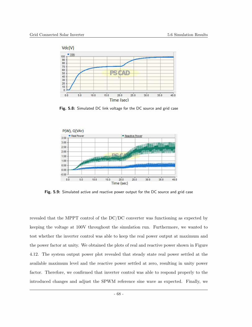
Grid Connected Solar Inverter 5.6 Simulation Results
Fig. 5.8: Simulated DC link voltage for the DC source and grid case
Fig. 5.9: Simulated active and reactive power output for the DC source and grid case
revealed that the MPPT control of the DC/DC converter was functioning as expected by
keeping the voltage at 100V throughout the simulation run. Furthermore, we wanted to
test whether the inverter control was able to keep the real power output at maximum and
the power factor at unity. We obtained the plots of real and reactive power shown in Figure
4.12. The system output power plot revealed that steady state real power settled at the
available maximum level and the reactive power settled at zero, resulting in unity power
factor. Therefore, we confirmed that inverter control was able to respond properly to the
introduced changes and adjust the SPWM reference sine wave as expected. Finally, we
- 68 -

Grid Connected Solar Inverter 5.6 Simulation Results
Fig. 5.10: Simulated current and voltage waveforms at the output of the system for theDC source and grid case
Fig. 5.11: Simulated DC link voltage for the PV panels and grid case
obtained output current and voltage waveforms, shown in Figure 4.13. We saw that both
current and voltage of the system were 60Hz sinusoidal waveforms. Also, current magnitude
did not exceed the 4A rating and the voltage was exactly 169V peak or 120Vrms, which
confirmed that our filter design was successful.
- 69 -

Grid Connected Solar Inverter 5.7 Simulation - Concluding Remarks
Fig. 5.12: Simulated active and reactive power flow for the PV panels and grid case
Fig. 5.13: Simulated current and voltage output of the system for the PV panels and gridcase
5.7 Simulation - Concluding Remarks
The results obtained from PSCAD simulation cases gave us a greater insight into the ex-
pected system performance throughout testing stages. For the initial testing stage, we
discovered that we could achieve a stable DC link voltage by manually setting the DC
source voltage or the duty cycle of the converter. The output filter response depended
on the connected load and the harmonic content of the system current and voltage was
significant. For the following testing stage with the grid connected, we discovered that we
- 70 -

Grid Connected Solar Inverter 5.7 Simulation - Concluding Remarks
were unable to achieve desired power factor regardless of the inverter control setup and,
also, the output waveforms were distorted. However, system operation was safe as long as
we monitored DC link voltage and the current flow in the system. Lastly, for testing with
the PV panels and the grid, simulation results showed that system operation was up to the
design specifications. We saw that the DC link voltage was maintained at 100V; maximum
power was extracted from the solar array and delivered to the grid at the desired power
factor and finally output current and voltage were sinusoidal. After completing the PSCAD
simulations we moved on to performing full system testing.
- 71 -

Grid Connected Solar Inverter 6. Overall System Testing and Troubleshooting
Chapter 6
Overall System Testing and
Troubleshooting
This section outlines the process of testing the hardware and software components together
and how the design and setup were modified to verify and improve system functionality.
The testing includes using LabVolt DC supply and RL load, applying SPWM signal to
Inverter module, improving switching signals, connecting to the grid and connecting the
Solar Panels.
6.1 Phase 1 - Using LabVolt DC supply and RL load
The objective of this test is to confirm whether a sinusoidal output can be generated when
the DC/DC converter, DC/AC inverter and filter are integrated together. For this test, we
used PWM signals from a function generator as oppose from the microcontroller to test the
hardware component of the system only.
- 72 -

Grid Connected Solar Inverter 6.1 Phase 1 - Using LabVolt DC supply and RL load
6.1.1 Test Setup and Procedure
Figure 6.1 shows the system setup used for testing the overall system. The hardware com-
ponents included DC/DC converter, DC/AC inverter, gate drivers, filter and transformer
to perform the test. In this test, a LabVolt DC source VIN was used to provide input to
the system and a RL load connected across the secondary of the transformer. The input
Fig. 6.1: Overall system testing setup
signals to the switches of both the converter and inverter were generated from a function
generator. We set the function generator to provide a square wave input with 3.3Vpk−pk and
1.65 V offset to simulate what the microcontroller is going to provide the converter and the
inverter. The DC/DC converter switching frequency was set to 3 kHz and the duty cycle to
66% which are the nominal frequency and duty cycle of the designed system respectively,
as discussed in section 3.2. On the other hand, the frequency input signal of the inverter
was set to 60 Hz with a duty cycle of 50 %.The test was conducted by first pre-charging
the Clink up to 30 V then the toggle switches that connect the converter and inverter were
closed.
6.1.2 Results and Discussion
Figure 6.1 shows the results obtained in using the labVolt DC supply and connecting a RL
load to the system. The voltage across the capacitor, VDC shown in blue, contains almost
- 73 -

Grid Connected Solar Inverter 6.1 Phase 1 - Using LabVolt DC supply and RL load
no ripple which verifies that the inverter is getting a good and stable DC input voltage
despite the non-ideal dc source VIN shown in yellow. Moreover, shown in red is the voltage
at the output of the filter, VOUT .
As expected, VOUT was not perfectly sinusoidal since the input we were feeding into
the inverter module was a 60Hz, 50% duty cycle square-wave from the function generator
instead of actual SPWM signals from the microcontroller. However, the objective of this
test was successfully accomplished. That is, we were able to confirm from the waveform of
VOUT that the hardware components of the system can generate waveforms that are closer
to a sinusoid as oppose to a square-wave.
Fig. 6.2: Using LabVolt DC supply and RL load
6.1.3 Problems Encountered
As soon as the toggle switches between the converter and inverter were closed, a sudden
drop in VDC was observed. This implies that the DC-link capacitor discharged to the RL
- 74 -
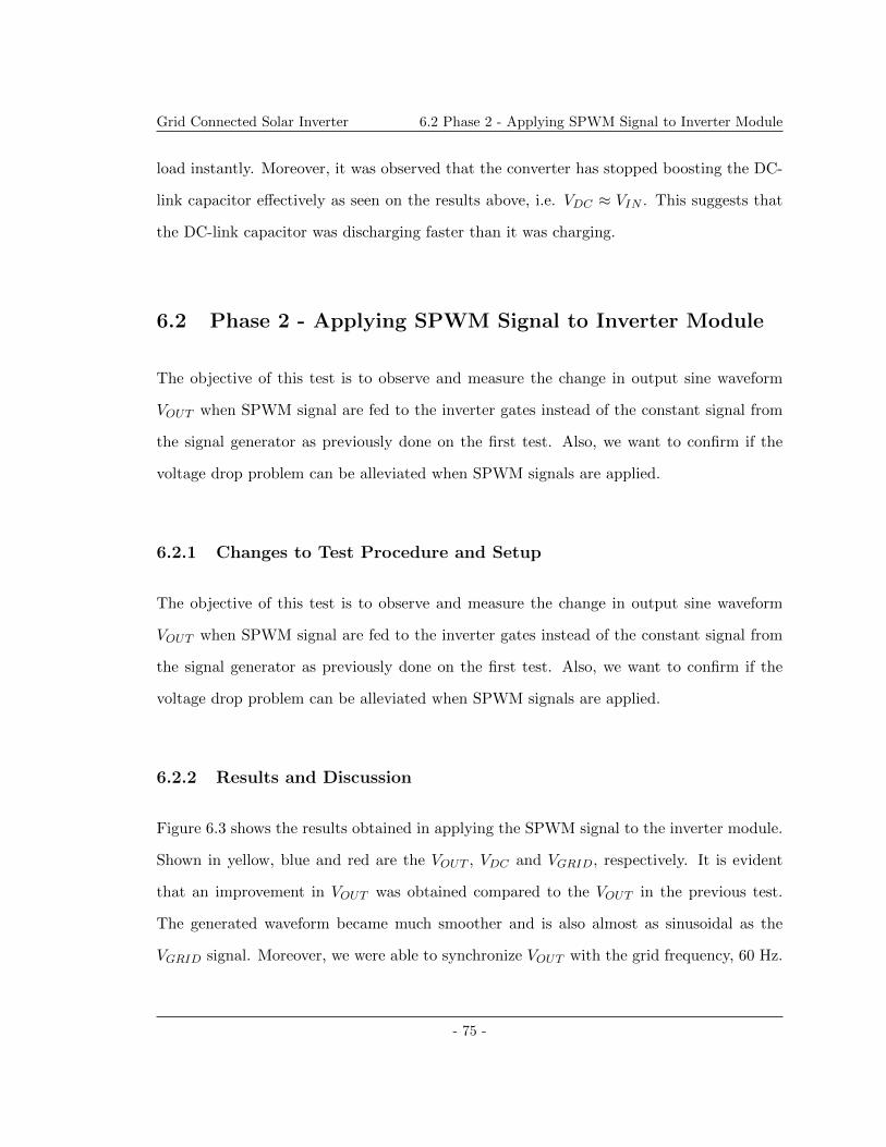
Grid Connected Solar Inverter 6.2 Phase 2 - Applying SPWM Signal to Inverter Module
load instantly. Moreover, it was observed that the converter has stopped boosting the DC-
link capacitor effectively as seen on the results above, i.e. VDC ≈ VIN . This suggests that
the DC-link capacitor was discharging faster than it was charging.
6.2 Phase 2 - Applying SPWM Signal to Inverter Module
The objective of this test is to observe and measure the change in output sine waveform
VOUT when SPWM signal are fed to the inverter gates instead of the constant signal from
the signal generator as previously done on the first test. Also, we want to confirm if the
voltage drop problem can be alleviated when SPWM signals are applied.
6.2.1 Changes to Test Procedure and Setup
The objective of this test is to observe and measure the change in output sine waveform
VOUT when SPWM signal are fed to the inverter gates instead of the constant signal from
the signal generator as previously done on the first test. Also, we want to confirm if the
voltage drop problem can be alleviated when SPWM signals are applied.
6.2.2 Results and Discussion
Figure 6.3 shows the results obtained in applying the SPWM signal to the inverter module.
Shown in yellow, blue and red are the VOUT , VDC and VGRID, respectively. It is evident
that an improvement in VOUT was obtained compared to the VOUT in the previous test.
The generated waveform became much smoother and is also almost as sinusoidal as the
VGRID signal. Moreover, we were able to synchronize VOUT with the grid frequency, 60 Hz.
- 75 -

Grid Connected Solar Inverter 6.3 Phase 3 - Improving the Switching Signal
Fig. 6.3: Result of applying SPWM signal to inverter module
6.2.3 Problems Encountered
The same issue was encountered in this test as the previous test; the converter stopped
boosting the voltage at the DC-bus as soon as the toggle switches between the converter
and inverter were closed. Moreover, there were spikes observed at the output waveform of
VOUT . We suspect that we are short circuiting the RL load which led to the occurrence of
the spikes. This suggests that there were glitches on the switching signals that were fed to
the IGBTs in the inverter module.
6.3 Phase 3 - Improving the Switching Signal
The objective of this test is to eliminate the spikes observed from Phase 2 by redesigning
the gate driver that will improve the switching signal delivered to the inverter module.
- 76 -

Grid Connected Solar Inverter 6.3 Phase 3 - Improving the Switching Signal
6.3.1 Changes to Test Setup
To resolve the issue discussed in 6.2.3, the gate driver circuit was redesigned to include
additional delay on the rising edges of the switching signals. This modification increased
the dead time of the switching and made sure that opposite IGBTs were never ON at the
same time. In addition, 0.1µF bypass capacitors were added close to the Vdd and Vss pins
of each IC chip to attenuate voltage fluctuations and noise in the power supplies.
The same test procedure was conducted in this test. That is, the DC-link capacitor
was initially pre-charged up to a certain value before closing the connection between the
converter and the inverter.
6.3.2 Results and Discussion
As a result of applying the design revision in the gate driver circuit, the waveforms shown
in Figure 6.4 were obtained. In blue is the VOUT while in yellow is the VDC . The main
observation that we witnessed on this test was that the boosting of the DC-link voltage
improved to 26.7% compared to the 4.5% from Phase 2. The improvement of the boosting
of VDC indicated that there were less losses in the inverter module compared to the Phase
2 testing previously conducted.
6.3.3 Problems Encountered
The problem we encountered in this test was that we failed to meet the main objective
of improving the spikes. Moreover, we started seeing distortions in VOUT . We observed
that as VIN was increased, the upper and lower halves of the sine output became more
imbalanced as shown in Figure 6.4. We are uncertain whether the additional delay circuit
that was added to the gate driver caused the distortion since the issue was never encountered
previously. However, we also understand that there could be other possible reasons for the
distortion which includes: saturation of the 1:2 transformer; grounding problem; and, noisy
- 77 -

Grid Connected Solar Inverter 6.4 Phase 4 - Connecting to the Grid
Fig. 6.4: Result of improving the switching signal
signal from the LabVolt source.
6.4 Phase 4 - Connecting to the Grid
The objective of this test is to observe the behaviour of the system when it is connected to
the grid as well as to measure the real and reactive power flow exchange between them. We
aim to transfer maximum real power to the grid which also means that the system should
ideally operate in unity power factor.
6.4.1 Test Procedure and Setup
Since we have already verified that the system is able to generate a sinusoidal output with
a 60 Hz frequency, we decided to connect the system to the grid as per the advice of
our supervisor. Figure 6.5 shows the new setup for testing the system. We replaced the
transformer we previously were using with a higher quality one that we are certain of not
saturating at the testing voltage. In addition, we used a variac that allowed us to vary and
- 78 -

Grid Connected Solar Inverter 6.4 Phase 4 - Connecting to the Grid
control the grid voltage that is connected to the secondary side of the transformer.
Fig. 6.5: Grid connection setup
The test was conducted by first turning up the grid voltage up to 10 V. As expected,
Clink was pre-charged and a negative power reading was measured across the primary side
of the transformer. The negative power implies that the system was absorbing power from
the grid at this point. Then, VIN was gradually increased to run both the converter and
inverter of the system.
6.4.2 Results and Discussion
Figure 6.6 shows the results obtained when the system was connected to the grid. Shown
in yellow is the VDC while shown in purple is voltage in between the transformer and the
variac, VSY S . The current that goes in between the transformer and the variac, ISY S was
also measured as well as the P and Q of the system. Notice that the PINV measured had
a positive value when VIN was introduced to the system. The positive P indicated that
the system had successfully pushed power to the grid. To further confirm the operation of
the system, the phase and amplitude of the reference waveform that controls the switching
of the inverter module was manually adjusted in the microcontroller. As a result, we were
able to effectively control the real power and the reactive power that we transfer to the
grid. Ultimately, this test have shown that we were able to push a real power, P , of 300
- 79 -

Grid Connected Solar Inverter 6.4 Phase 4 - Connecting to the Grid
mW and a small reactive power, Q, of 58 mVAr to the grid. The P and Q values result in
a power factor equivalent to 0.98 which is very close to the desired unity power factor we
were aiming for.
Fig. 6.6: Result of connecting the system to the grid
6.4.3 Problems Encountered
The output power specification of the system is 300 W. We observed that as we increase
VIN , the output power P increased as well. However, as shown on the results of this test, the
output waveform Vsys we generated still contained spikes which may damage the equipment.
For this reason, we deemed it unsafe to further increase the voltage input. Thereby, we were
not able to transfer more power to the system.
- 80 -

Grid Connected Solar Inverter 6.5 Phase 5 - Connecting the Solar Panels
6.5 Phase 5 - Connecting the Solar Panels
The objective of this test is to integrate the solar panels to the system and test the developed
MPPT algorithm. We aim to extract the maximum available power from the panels and
transfer it to the grid. Unfortunately, this test was not performed in time due to test
setup difficulties particularly in timing ideal sunlight and weather condition. Moreover,
transporting the whole hardware system itself posed a challenge to us since equipment for
measuring high voltage and current are not available outside the laboratory. We plan to
perform further testing prior to the final presentation in order to verify all the specifications
set in this project.
6.6 Overall System Testing - Concluding Remarks
The overall system testing underwent several troubleshooting stages. On the first phase of
testing, the functionality of the hardware portion of the system was verified. On the second
phase of testing, the operation of the SPWM software with the hardware was confirmed. For
both of these phases, we observed that the dc-bus was not being boosted effectively during
operation. This was later improved on the third phase of testing when the switching signal of
the inverter was modified. However, distortions started occurring at the waveform output.
On the fourth phase of testing, we connected the system to the grid. On this test, we were
successfully able to push real and reactive power of 300 mW and 0.058 mVAR, respectively,
to the grid. Although these values are way below the power output specification, we were
successfully able to meet our desired power factor since the P and Q we measured results
in a power factor of 0.98 which is very close to unity. And finally, for the fifth phase of
testing, we wanted to integrate the solar panels to the system and transfer power to the
grid. This test, however, was not performed in time due to test setup difficulty.
- 81 -
Grid Connected Solar Inverter 7. Conclusions
Chapter 7
Conclusions
Overall, the individual subsystems of the project such as the DC/DC converter, DC/AC
inverter, Gate Drivers, and the control system have been designed, built, and tested. The
results are discussed in section 3 of the report and prove that the items perform as intended.
System Hardware interface testing was performed and results verified the intended function-
ality based on the design calculations and the project specifications. The Hardware-Software
Integration was the next step which included the integration of the software intended for the
DC/DC converter, DC/AC inverter, and the gate drivers with their respective hardware.
This stage was carried out successfully for the DC/AC inverter and the gate drivers. That
said, the Software Hardware Integration stage remains to be completely done pending the
integration of the MPPT software with the converter. Overall system testing was performed
and the system excluding the solar panels was able to connect with the grid and push power
as well as being able to synchronize with the grid. Problems were encountered and these
challenges were discussed earlier in section 5. The project budget assigned to the team
was 500andapproximately475 has been used. All financial record have been documented in
table x under Appendix x. There are a few tests that remain to be completed prior to the
final presentation which include the MPPT integration with the DC/DC converter, higher
- 82 -

Grid Connected Solar Inverter
output power to the grid, and full system testing including the solar panels. The team
would recommend future design groups to consider real life applications in different climate
conditions where hydro power is not as accessible as it is in Manitoba. This will provide an
opportunity for the group to consider different specifications and a larger customer base. By
customer base, we propose that such environmentally friendly solutions should be developed
for more economically feasible situations. At last, additional features are to be evaluated
and possibly implemented by future design group and these features could include battery
charging and newer solar energy products.
- 83 -

Grid Connected Solar Inverter REFERENCES
References
[1] Saadat, Hadi , Power System Analysis. McGraw-Hill ed , Vol, 1999.
[2] Jonathan Adams, Bootstrap Component Selection For Control ICs[online] September 42001, Accessed: October 2013
[3] Freescale, General Function Library [online] 2011, Accessed: September 2013
[4] IEEE standards coordinating committee 21, IEEE standard for interconnecting dis-tributed resources with electric power systems [online] April 15, 2009, Accessed: Septem-ber 2013
[5] Letti, J. and Bauer, J. and Linhart, L., Comparison of Different Filter Types for GridConnected Inverter [online] March 20, 2011, Accessed: September 2013
[6] Daniel W. Hart, Power Electronics. McGraw-Hill, New York, 3rd Edition, pp. 373-376,2011.
[7] Robert, Kropp., Solar expected to maintain its status as the world’s fastest-growingenergy technology, (Social Funds), [online] March 3, 2009, Accessed: September 2013
[8] Weng, K. W., Cytron Technologies Tutorials PID for Embedded Design, [online], 2010,Accessed: October 2013
[9] Blake, C. and Bull, C., International Rectifier, IGBT or MOSFET: Choose Wisely,[online], Accessed: September 2013
[10] Microcontroller for better live, Microcontroller based Power Monitoring, [online], 2012,Accessed: November 2013
[11] Kinsner, W., Microprocessor and Microcomputer Interfacing for Real-Time Systems,University of Manitoba, Canada, 2013
[12] Manitoba Hydro, Interconnection Guideline, For Connecting Distributed Resources ToThe Manitoba Hydro Distribution System, [online], 2003, Accessed: September 2013
[13] ”TWR-56F8400: DSC MC56F84789 motor and power control tower”,freescale,[online], Accessed: September 2013
- 84 -

Grid Connected Solar Inverter A. First Appendix
- 85 -

Grid Connected Solar Inverter
Appendix A
Budget Summary
Fig. A.1: Budget
- 86 -

Grid Connected Solar Inverter
Fig. A.2: Budget continued
- 87 -

Grid Connected Solar Inverter B. Second Appendix
Appendix B
Second Appendix
The entire software code is saved on a disk and attached to this report. The disk includesthe inverter project folder which can be imported into Freescale’s CodeWarrior DevelopmentStudio. Additionally, the disk includes a readme.txt file that contains instructions on howto compile and run the project.
- 88 -