Impact of temperature cycle profile on fatigue life of ... · Impact of Temperature Cycle Profile...
6
IEEE TRANSACTIONS ON ADVANCED PACKAGING, VOL. 25, NO. 3, AUGUST 2002 433 Impact of Temperature Cycle Profile on Fatigue Life of Solder Joints Terry Dishongh, Cemal Basaran, Alexander N. Cartwright, Member, IEEE, Ying Zhao, and Heng Liu, Student Member, IEEE Abstract—In this paper the influence of the temperature cycle time history profile on the fatigue life of ball grid array (BGA) solder joints is studied. Temperature time history in a Pentium pro- cessor laptop computer was measured for a three-month period by means of thermocouples placed inside the computer. In addi- tion, pentium BGA packages were subjected to industry standard temperature cycles and also to in-situ measured temperature cycle profiles. Inelastic strain accumulation in each solder joint during thermal cycling was measured by high sensitivity Moiré interfer- ometry technique. Results indicate that fatigue life of the solder joint is not independent of the temperature cycle profile used. In- dustry standard temperature cycle profile leads to conservative fa- tigue life observations by underestimating the actual number of cycles to failure. Index Terms—BGA packaging, Moiré interferometry, solder joints fatigue, temperature cycle profile. I. INTRODUCTION T HE RELIABILITY of microelectronic packaging solder joints is critical to quality and integrity of electronic de- vices. Ball grid array (BGA) packaging is becoming one of the most popular electronic packages in the microelectronics in- dustry, due to its many advantages over all other packaging tech- nologies. The Pb/Sn eutectic solder alloy is widely used as a joining material. It is well known that the dominant failure mode for solder joints is low cycle thermal fatigue, which is caused by thermal expansion mismatch between the bonded components and heat dissipated by devices during operation. Although the thermomechanical response of solder joints under thermal cycling has been studied extensively, Basaran et al. [1], [2] presents an extensive literature survey on the subject, the impact and effect of temperature fluctuations during dwell times on BGA solder joint fatigue life has never been studied or reported in the literature. The main question in reliability studies has always been; is temperature cycling appropriate both in the time history profile and magnitude if we are unsure of the damage mechanism and strain field in the Manuscript received November 6, 2000; revised August 1, 2002. This work was supported in part by Intel Corporation and the National Science Foundation CMS-Material Processing and Surface Engineering Program Grant 9908016. T. Dishongh is with Intel Corporation, Hillsboro, OR 97124-6497 USA. C. Basaran, A. N. Cartwright, and H. Liu are with the Electronic Packaging Laboratory, State University of New York at Buffalo, Buffalo, NY 14260-1920 USA (e-mail: [email protected]). Y. Zhao was with the Electronic Packaging Laboratory, State University of New York at Buffalo, Buffalo, NY 14260-1920 USA. She is now with Analog Devices, Norwood, MA 02062-9106 USA. Digital ObjectIdentifier 10.1109/TADVP.2002.806735 solder joint? What is the baseline of inelastic strains developed in thermal cycling and usage? Until now these questions remain unanswered because of a lack of a technique to measure the strain field in solder joint in fatigue testing. Temperature cycling is used as a standard industry practice for determining the thermomechanical fatigue life and relia- bility of solder joints [3]–[5]. Testing under thermal cycling conditions is a vehicle to accelerate the fatigue failure mech- anism. The test yields the number of cycles to the failure value. Yet thermal cycling alone does not give any local information about the failure mechanism in the solder joint. On the other hand high sensitivity Moiré interferometry provides whole field maps of in-plane deformation contours with sub micron resolu- tion, and provides both normal and shear strains. Such capability is extremely useful for studying thermomechanical behavior of solder joints in electronic packaging. A Moiré interferometry technology developed in the UB Electronic Packaging Labora- tory allows recording of inelastic strain accumulations for cyclic thermomechanical loading. As inelastic deformation is directly related to fatigue life of solder joints, the inelastic strain accu- mulation can be used to evaluate solder joint fatigue life perfor- mance. II. EXPERIMENTAL PROCEDURE The industry standard temperature profile have a jigsaw shape with dwell times at maximum and minimum temperatures as shown in Fig. 1(a). The conventional temperature time histo- ries are based on many assumptions that have no technical or empirical basis. During this study several Pentium Processor based laptop computers were wired with thermocouples in two different locations for a three-month period. One thermocouple was on the thermal plate of the processor and the other was on the motherboard away from the VR on the PCB. Temperature time histories were recorded. The observation indicates that the actual temperature profile experienced by the package is dif- ferent than traditional temperature time histories used for tem- perature cycling tests in the industry. Fig. 1(b) and (c) were ob- tained from the in-situ field measurements. The purpose of this study is to compare the influence of the temperature time history profile on the fatigue life of BGA solder joints. In this study an industry standard temperature profile as well as the in-situ measured actual temperature time histories are used for thermal cycling. Three different temperature profiles were used. Test 1 has a conventional thermal cycling profile, Fig. 1(a). For Test 2 and Test 3 the temperature profiles include temperature fluctuations 1521-3323/02$17.00 © 2002 IEEE Authorized licensed use limited to: IEEE Xplore. Downloaded on October 9, 2008 at 22:59 from IEEE Xplore. Restrictions apply.
Transcript of Impact of temperature cycle profile on fatigue life of ... · Impact of Temperature Cycle Profile...
IEEE TRANSACTIONS ON ADVANCED PACKAGING, VOL. 25, NO. 3, AUGUST 2002 433
Impact of Temperature Cycle Profile on Fatigue Lifeof Solder Joints
Terry Dishongh, Cemal Basaran, Alexander N. Cartwright, Member, IEEE, Ying Zhao, andHeng Liu, Student Member, IEEE
Abstract—In this paper the influence of the temperature cycletime history profile on the fatigue life of ball grid array (BGA)solder joints is studied. Temperature time history in a Pentium pro-cessor laptop computer was measured for a three-month periodby means of thermocouples placed inside the computer. In addi-tion, pentium BGA packages were subjected to industry standardtemperature cycles and also toin-situ measured temperature cycleprofiles. Inelastic strain accumulation in each solder joint duringthermal cycling was measured by high sensitivity Moiré interfer-ometry technique. Results indicate that fatigue life of the solderjoint is not independent of the temperature cycle profile used. In-dustry standard temperature cycle profile leads to conservative fa-tigue life observations by underestimating the actual number ofcycles to failure.
Index Terms—BGA packaging, Moiré interferometry, solderjoints fatigue, temperature cycle profile.
I. INTRODUCTION
T HE RELIABILITY of microelectronic packaging solderjoints is critical to quality and integrity of electronic de-
vices. Ball grid array (BGA) packaging is becoming one of themost popular electronic packages in the microelectronics in-dustry, due to its many advantages over all other packaging tech-nologies.
The Pb/Sn eutectic solder alloy is widely used as a joiningmaterial. It is well known that the dominant failure mode forsolder joints is low cycle thermal fatigue, which is caused bythermal expansion mismatch between the bonded componentsand heat dissipated by devices during operation.
Although the thermomechanical response of solder jointsunder thermal cycling has been studied extensively, Basaranet al. [1], [2] presents an extensive literature survey on thesubject, the impact and effect of temperature fluctuationsduring dwell times on BGA solder joint fatigue life has neverbeen studied or reported in the literature. The main questionin reliability studies has always been; is temperature cyclingappropriate both in the time history profile and magnitude ifwe are unsure of the damage mechanism and strain field in the
Manuscript received November 6, 2000; revised August 1, 2002. This workwas supported in part by Intel Corporation and the National Science FoundationCMS-Material Processing and Surface Engineering Program Grant 9908016.
T. Dishongh is with Intel Corporation, Hillsboro, OR 97124-6497 USA.C. Basaran, A. N. Cartwright, and H. Liu are with the Electronic Packaging
Laboratory, State University of New York at Buffalo, Buffalo, NY 14260-1920USA (e-mail: [email protected]).
Y. Zhao was with the Electronic Packaging Laboratory, State University ofNew York at Buffalo, Buffalo, NY 14260-1920 USA. She is now with AnalogDevices, Norwood, MA 02062-9106 USA.
Digital Object Identifier 10.1109/TADVP.2002.806735
solder joint? What is the baseline of inelastic strains developedin thermal cycling and usage? Until now these questions remainunanswered because of a lack of a technique to measure thestrain field in solder joint in fatigue testing.
Temperature cycling is used as a standard industry practicefor determining the thermomechanical fatigue life and relia-bility of solder joints [3]–[5]. Testing under thermal cyclingconditions is a vehicle to accelerate the fatigue failure mech-anism. The test yields the number of cycles to the failure value.Yet thermal cycling alone does not give any local informationabout the failure mechanism in the solder joint. On the otherhand high sensitivity Moiré interferometry provides whole fieldmaps of in-plane deformation contours with sub micron resolu-tion, and provides both normal and shear strains. Such capabilityis extremely useful for studying thermomechanical behavior ofsolder joints in electronic packaging. A Moiré interferometrytechnology developed in the UB Electronic Packaging Labora-tory allows recording of inelastic strain accumulations for cyclicthermomechanical loading. As inelastic deformation is directlyrelated to fatigue life of solder joints, the inelastic strain accu-mulation can be used to evaluate solder joint fatigue life perfor-mance.
II. EXPERIMENTAL PROCEDURE
The industry standard temperature profile have a jigsaw shapewith dwell times at maximum and minimum temperatures asshown in Fig. 1(a). The conventional temperature time histo-ries are based on many assumptions that have no technical orempirical basis. During this study several Pentium Processorbased laptop computers were wired with thermocouples in twodifferent locations for a three-month period. One thermocouplewas on the thermal plate of the processor and the other was onthe motherboard away from the VR on the PCB. Temperaturetime histories were recorded. The observation indicates that theactual temperature profile experienced by the package is dif-ferent than traditional temperature time histories used for tem-perature cycling tests in the industry. Fig. 1(b) and (c) were ob-tained from thein-situ field measurements.
The purpose of this study is to compare the influence of thetemperature time history profile on the fatigue life of BGAsolder joints. In this study an industry standard temperatureprofile as well as thein-situ measured actual temperature timehistories are used for thermal cycling.
Three different temperature profiles were used. Test 1 has aconventional thermal cycling profile, Fig. 1(a). For Test 2 andTest 3 the temperature profiles include temperature fluctuations
1521-3323/02$17.00 © 2002 IEEE
Authorized licensed use limited to: IEEE Xplore. Downloaded on October 9, 2008 at 22:59 from IEEE Xplore. Restrictions apply.
434 IEEE TRANSACTIONS ON ADVANCED PACKAGING, VOL. 25, NO. 3, AUGUST 2002
Fig. 1. Temperature time histories used in this study.
at the highest temperature, Fig. 1(b) and (c). For each test (tem-perature profile) 5 specimens were used to validate the results.Test conditions for the three tests are as follows.
• Test 1: Temperature profile is between 0C to 75 C with30 minutes dwells on both sides of the curve.
• Test 2: Temperature profile is between 0C to 75 C with30 min of 5 mini-cycles at 10 C on the hot side and 30min dwell on the cold side.
• Test 3: Temperature profile is between 0C to 75 C with30 min of 15 mini-cycles at 5 C on the hot side and 30min dwell on the cold side.
The temperature cycling period was 70 min/cycle. Each testwas performed independently on five BGA packages, and eachsample was cycled 100 thermal cycles. For each sample theMoiré interferometry strain field measurement was performedat every 20 cycles. SEM micrographs were taken at the begin-ning and the end of cycling. Moiré fringes give us the inelasticstrain accumulation.
III. M OIRÉ INTERFEROMETER
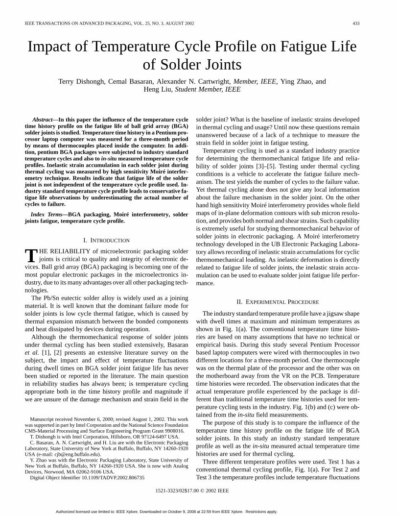
The Moiré Interferometry (MI) and the imaging systems usedfor sub micron displacement measurement are described in de-tail in [6], [7]. The fringe pattern can be related to in-plane in-
Fig. 2. Optical setup.
elastic strains quantitatively as given in [8]
(1)
(2)
(3)
where is the displacement in the direction; is the dis-placement in the direction. is the horizontal fringe order,and is the vertical fringe order. In this project, each fringe
Authorized licensed use limited to: IEEE Xplore. Downloaded on October 9, 2008 at 22:59 from IEEE Xplore. Restrictions apply.
DISHONGHet al.: IMPACT OF TEMPERATURE CYCLE PROFILE ON FATIGUE LIFE OF SOLDER JOINTS 435
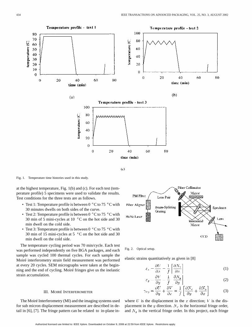
Fig. 3. Four step phase shifting example (n = 14, 1=f = 29:8 nm).
represents m in this study. The deformation sen-sitivity can be improved further by introducing phase shiftingalgorithms. The fringe patterns in this case can be written as
(4)
where is the background illumination, is the fringe visi-bility, is the phase generated by the specimen andis theadditional phase shift applied in order to extract the phase dis-tribution. Since there are only three unknown variables,,and in Equation (4), three steps of phase shifting should besufficient to solve them completely. The optics setup of phaseshifting Moiré is described in Fig. 2. Additional phase shiftscan be easily introduced by moving the beam splitting gratingin the , direction to achieve the desired amount. The improve-ment of sensitivity is illustrated in an example of the most basicfour step phase shifting algorithm, i.e., , /2, , and 3 /2where the corresponding grating position is 0, 0.104m, 0.208
m, 0.312 m respectively. The example fringe in Fig. 3 is of a2.9 mm 6.3 mm area. The deformation sensitivity of the lastimage is 29.8 nm, i.e., each fringe represents 29.8 nm relativedeformation. Besides the simple four-step method, there existmany other phase shifting algorithms, such as 33, 7 steps,Schwilder–Hariharan, Angel and Wizinowich (21) and Carréetc. Different algorithms have their own advantages and disad-vantages in terms of resistance to phase shifting error (vibration,phase miscalibration, detector nonlinearity and stray light, forinstance), as well as the cost of extra instruments and the algo-
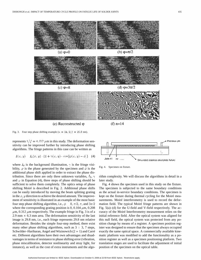
Fig. 4. Specimen on fixture.
rithm complexity. We will discuss the algorithms in detail in alater study.
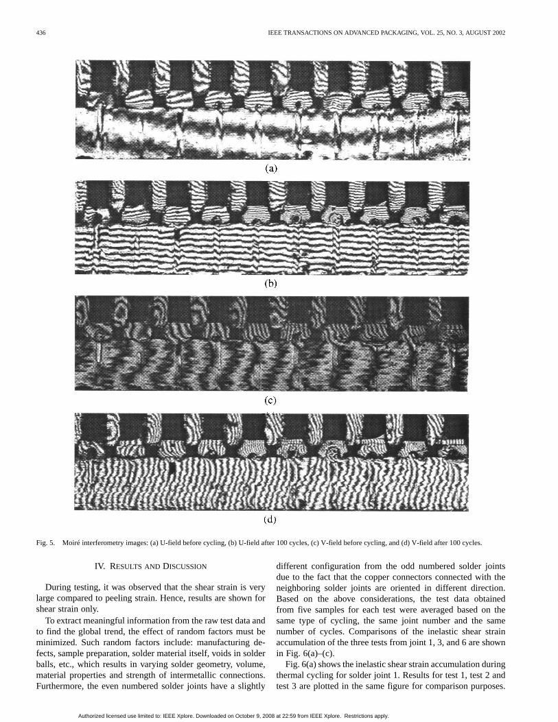
Fig. 4 shows the specimen used in this study on the fixture.The specimen is subjected to the same boundary conditionsas the actual in-service boundary conditions. The specimen iskept on the fixture during thermal cycling for the Moiré mea-surements. Moiré interferometry is used to record the defor-mation field. The typical Moiré fringe patterns are shown inFig. 5(a)–(d) for the U-field and V-field respectively. The ac-curacy of the Moiré Interferometry measurement relies on theinitial reference field. After the optical system was aligned forthis null field, the optical system was protected from any po-sition change by means of a register. A specimen position reg-ister was designed to ensure that the specimen always occupiedexactly the same optical space. A commercially available kine-matic platform was modified to add the functionality as a po-sition register as well as a specimen positioning platform. Twotranslation stages are used to facilitate the adjustment of initialposition of the specimen on the optical table.
Authorized licensed use limited to: IEEE Xplore. Downloaded on October 9, 2008 at 22:59 from IEEE Xplore. Restrictions apply.
436 IEEE TRANSACTIONS ON ADVANCED PACKAGING, VOL. 25, NO. 3, AUGUST 2002
Fig. 5. Moiré interferometry images: (a) U-field before cycling, (b) U-field after 100 cycles, (c) V-field before cycling, and (d) V-field after 100 cycles.
IV. RESULTS AND DISCUSSION
During testing, it was observed that the shear strain is verylarge compared to peeling strain. Hence, results are shown forshear strain only.
To extract meaningful information from the raw test data andto find the global trend, the effect of random factors must beminimized. Such random factors include: manufacturing de-fects, sample preparation, solder material itself, voids in solderballs, etc., which results in varying solder geometry, volume,material properties and strength of intermetallic connections.Furthermore, the even numbered solder joints have a slightly
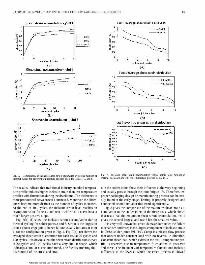
different configuration from the odd numbered solder jointsdue to the fact that the copper connectors connected with theneighboring solder joints are oriented in different direction.Based on the above considerations, the test data obtainedfrom five samples for each test were averaged based on thesame type of cycling, the same joint number and the samenumber of cycles. Comparisons of the inelastic shear strainaccumulation of the three tests from joint 1, 3, and 6 are shownin Fig. 6(a)–(c).
Fig. 6(a) shows the inelastic shear strain accumulation duringthermal cycling for solder joint 1. Results for test 1, test 2 andtest 3 are plotted in the same figure for comparison purposes.
Authorized licensed use limited to: IEEE Xplore. Downloaded on October 9, 2008 at 22:59 from IEEE Xplore. Restrictions apply.
DISHONGHet al.: IMPACT OF TEMPERATURE CYCLE PROFILE ON FATIGUE LIFE OF SOLDER JOINTS 437
Fig. 6. Comparison of inelastic shear strain accumulation versus number ofthermal cycles for different temperature profiles at solder joints 1, 3, and 6.
The results indicate that traditional industry standard tempera-ture profile induces higher inelastic strain than test temperatureprofiles with fluctuation during the dwell time. The difference ismore pronounced between test 1 and test 3. Moreover, the differ-ences become more distinct as the number of cycles increases.At the end of 100 cycles, the inelastic strain level reaches anasymptotic value for test 2 and test 3 while test 1 curve have amuch larger positive slope.
Fig. 6(b)–(f) show the inelastic strain accumulation duringthermal cycling for solder joints 3 and 6. Strain is the largest injoint 1 (outer edge joint), hence failure usually initiates at joint1, for the configuration given in Fig. 4. Fig. 7(a)–(c) shows theaveraged shear strain distribution for each test at 20 cycles and100 cycles. It is obvious that the shear strain distribution curvesat 20 cycles and 100 cycles have a very similar shape, whichindicates a similar distribution trend. The factors affecting thedistribution of the stress and strai
Fig. 7. Inelastic shear strain accumulation versus solder joint number atthermal cycles 20 and 100 for temperature profiles 1, 2, and 3.
n in the solder joints show their influence at the very beginningand usually persist through the joint fatigue life. Therefore, im-proper packaging design or manufacturing process can be usu-ally found at the early stage. Testing, if properly designed andconducted, should not alter this trend significantly.
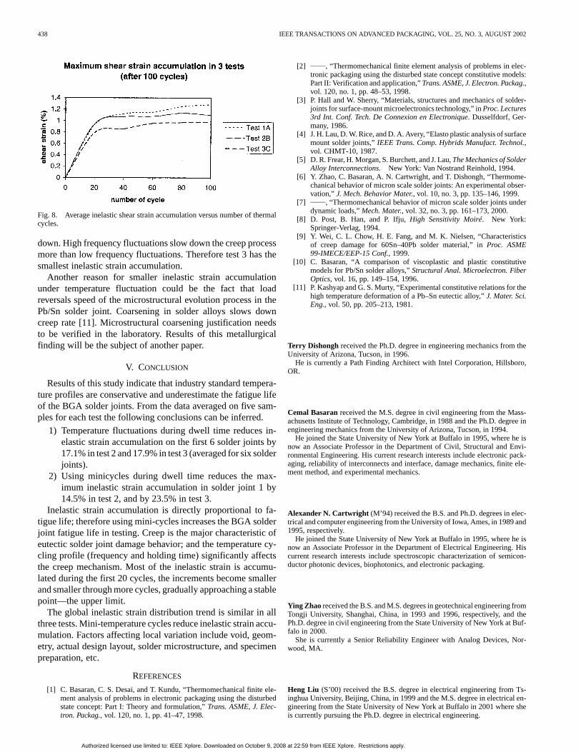
Fig. 8 gives the comparison of the maximum shear strain ac-cumulation in the solder joints in the three tests, which showsthat test 1 has the maximum shear strain accumulation, test 2gives the second largest, and test 3 has the smallest value.
It is very well known that creep-damage dominates the failuremechanism and creep is the largest component of inelastic strainin Pb/Sn solder joints [9], [10]. Creep is a plastic flow processthat occurs under constant load with no reversal in direction.Constant shear load, which exists in the test 1 temperature pro-file, is reversed due to temperature fluctuations in tests twoand three. The frequency of temperature fluctuations makes adifference in the level at which the creep process is slowed
Authorized licensed use limited to: IEEE Xplore. Downloaded on October 9, 2008 at 22:59 from IEEE Xplore. Restrictions apply.
438 IEEE TRANSACTIONS ON ADVANCED PACKAGING, VOL. 25, NO. 3, AUGUST 2002
Fig. 8. Average inelastic shear strain accumulation versus number of thermalcycles.
down. High frequency fluctuations slow down the creep processmore than low frequency fluctuations. Therefore test 3 has thesmallest inelastic strain accumulation.
Another reason for smaller inelastic strain accumulationunder temperature fluctuation could be the fact that loadreversals speed of the microstructural evolution process in thePb/Sn solder joint. Coarsening in solder alloys slows downcreep rate [11]. Microstructural coarsening justification needsto be verified in the laboratory. Results of this metallurgicalfinding will be the subject of another paper.
V. CONCLUSION
Results of this study indicate that industry standard tempera-ture profiles are conservative and underestimate the fatigue lifeof the BGA solder joints. From the data averaged on five sam-ples for each test the following conclusions can be inferred.
1) Temperature fluctuations during dwell time reduces in-elastic strain accumulation on the first 6 solder joints by17.1% in test 2 and 17.9% in test 3 (averaged for six solderjoints).
2) Using minicycles during dwell time reduces the max-imum inelastic strain accumulation in solder joint 1 by14.5% in test 2, and by 23.5% in test 3.
Inelastic strain accumulation is directly proportional to fa-tigue life; therefore using mini-cycles increases the BGA solderjoint fatigue life in testing. Creep is the major characteristic ofeutectic solder joint damage behavior; and the temperature cy-cling profile (frequency and holding time) significantly affectsthe creep mechanism. Most of the inelastic strain is accumu-lated during the first 20 cycles, the increments become smallerand smaller through more cycles, gradually approaching a stablepoint—the upper limit.
The global inelastic strain distribution trend is similar in allthree tests. Mini-temperature cycles reduce inelastic strain accu-mulation. Factors affecting local variation include void, geom-etry, actual design layout, solder microstructure, and specimenpreparation, etc.
REFERENCES
[1] C. Basaran, C. S. Desai, and T. Kundu, “Thermomechanical finite ele-ment analysis of problems in electronic packaging using the disturbedstate concept: Part I: Theory and formulation,”Trans. ASME, J. Elec-tron. Packag., vol. 120, no. 1, pp. 41–47, 1998.
[2] , “Thermomechanical finite element analysis of problems in elec-tronic packaging using the disturbed state concept constitutive models:Part II: Verification and application,”Trans. ASME, J. Electron. Packag.,vol. 120, no. 1, pp. 48–53, 1998.
[3] P. Hall and W. Sherry, “Materials, structures and mechanics of solder-joints for surface-mount microelectronics technology,” inProc. Lectures3rd Int. Conf. Tech. De Connexion en Electronique. Dusselfdorf, Ger-many, 1986.
[4] J. H. Lau, D. W. Rice, and D. A. Avery, “Elasto plastic analysis of surfacemount solder joints,”IEEE Trans. Comp. Hybrids Manufact. Technol.,vol. CHMT-10, 1987.
[5] D. R. Frear, H. Morgan, S. Burchett, and J. Lau,The Mechanics of SolderAlloy Interconnections. New York: Van Nostrand Reinhold, 1994.
[6] Y. Zhao, C. Basaran, A. N. Cartwright, and T. Dishongh, “Thermome-chanical behavior of micron scale solder joints: An experimental obser-vation,” J. Mech. Behavior Mater., vol. 10, no. 3, pp. 135–146, 1999.
[7] , “Thermomechanical behavior of micron scale solder joints underdynamic loads,”Mech. Mater., vol. 32, no. 3, pp. 161–173, 2000.
[8] D. Post, B. Han, and P. Ifju,High Sensitivity Moiré. New York:Springer-Verlag, 1994.
[9] Y. Wei, C. L. Chow, H. E. Fang, and M. K. Nielsen, “Characteristicsof creep damage for 60Sn–40Pb solder material,” inProc. ASME99-IMECE/EEP-15 Conf., 1999.
[10] C. Basaran, “A comparison of viscoplastic and plastic constitutivemodels for Pb/Sn solder alloys,”Structural Anal. Microelectron. FiberOptics, vol. 16, pp. 149–154, 1996.
[11] P. Kashyap and G. S. Murty, “Experimental constitutive relations for thehigh temperature deformation of a Pb–Sn eutectic alloy,”J. Mater. Sci.Eng., vol. 50, pp. 205–213, 1981.
Terry Dishongh received the Ph.D. degree in engineering mechanics from theUniversity of Arizona, Tucson, in 1996.
He is currently a Path Finding Architect with Intel Corporation, Hillsboro,OR.
Cemal Basaranreceived the M.S. degree in civil engineering from the Mass-achusetts Institute of Technology, Cambridge, in 1988 and the Ph.D. degree inengineering mechanics from the University of Arizona, Tucson, in 1994.
He joined the State University of New York at Buffalo in 1995, where he isnow an Associate Professor in the Department of Civil, Structural and Envi-ronmental Engineering. His current research interests include electronic pack-aging, reliability of interconnects and interface, damage mechanics, finite ele-ment method, and experimental mechanics.
Alexander N. Cartwright (M’94) received the B.S. and Ph.D. degrees in elec-trical and computer engineering from the University of Iowa, Ames, in 1989 and1995, respectively.
He joined the State University of New York at Buffalo in 1995, where he isnow an Associate Professor in the Department of Electrical Engineering. Hiscurrent research interests include spectroscopic characterization of semicon-ductor photonic devices, biophotonics, and electronic packaging.
Ying Zhao received the B.S. and M.S. degrees in geotechnical engineering fromTongji University, Shanghai, China, in 1993 and 1996, respectively, and thePh.D. degree in civil engineering from the State University of New York at Buf-falo in 2000.
She is currently a Senior Reliability Engineer with Analog Devices, Nor-wood, MA.
Heng Liu (S’00) received the B.S. degree in electrical engineering from Ts-inghua University, Beijing, China, in 1999 and the M.S. degree in electrical en-gineering from the State University of New York at Buffalo in 2001 where sheis currently pursuing the Ph.D. degree in electrical engineering.
Authorized licensed use limited to: IEEE Xplore. Downloaded on October 9, 2008 at 22:59 from IEEE Xplore. Restrictions apply.