IMPACT OF MECHANICAL STRESS ON ALGAN/GAN HEMT … · impact of mechanical stress on algan/gan hemt...
126
1 IMPACT OF MECHANICAL STRESS ON ALGAN/GAN HEMT PERFORMANCE: CHANNEL RESISTANCE AND GATE CURRENT By ANDREW DANIEL KOEHLER A DISSERTATION PRESENTED TO THE GRADUATE SCHOOL OF THE UNIVERSITY OF FLORIDA IN PARTIAL FULFILLMENT OF THE REQUIREMENTS FOR THE DEGREE OF DOCTOR OF PHILOSOPHY UNIVERSITY OF FLORIDA 2011
Transcript of IMPACT OF MECHANICAL STRESS ON ALGAN/GAN HEMT … · impact of mechanical stress on algan/gan hemt...
1
IMPACT OF MECHANICAL STRESS ON ALGAN/GAN HEMT PERFORMANCE: CHANNEL RESISTANCE AND GATE CURRENT
By
ANDREW DANIEL KOEHLER
A DISSERTATION PRESENTED TO THE GRADUATE SCHOOL OF THE UNIVERSITY OF FLORIDA IN PARTIAL FULFILLMENT
OF THE REQUIREMENTS FOR THE DEGREE OF DOCTOR OF PHILOSOPHY
UNIVERSITY OF FLORIDA
2011

2
© 2011 Andrew Daniel Koehler

3
To my family

4
ACKNOWLEDGMENTS
I would like to thank my advisor Dr. Scott E. Thompson. I have benefited from his
advice and guidance during my studies. Also, I thank my co-chair Dr. Toshikazu
Nishida for his encouragement and guidance. I would also like to thank Dr. Ant Ural
and Dr. Brent Gila for their assistance and serving on my committee.
I also thank all of my current and past colleagues for their assistance and support:
Amit, Eric, Guangyu, Hyunwoo, Jingjing, Ji-Song, Kehuey, Lu, Min, Nidhi, Onur, Sagar,
Sri, Tony, Toshi, Ukjin, Uma, Xiaodong, Yongke, Younsung.
5
TABLE OF CONTENTS
page
ACKNOWLEDGMENTS .................................................................................................. 4
LIST OF TABLES ............................................................................................................ 7
LIST OF FIGURES .......................................................................................................... 8
LIST OF ABBREVIATIONS ........................................................................................... 12
ABSTRACT ................................................................................................................... 13
CHAPTER
1 INTRODUCTION AND OVERVIEW ....................................................................... 15
Overview of AlGaN/GaN HEMTs ............................................................................ 15
Stress in AlGaN/GaN HEMTs ................................................................................. 17
Stress in Semiconductor Technology ..................................................................... 18
Motivation ............................................................................................................... 19
Organization ........................................................................................................... 21
2 ALGAN/GAN HEMT AND WAFER BENDING BACKGROUND ............................. 25
GaN Fundamentals ................................................................................................. 25
Spontaneous Polarization ................................................................................. 25
Piezoelectric Polarization ................................................................................. 26
Formation of 2DEG .......................................................................................... 28
Device Description .................................................................................................. 29
Mechanical Wafer Bending Experiment Setup ........................................................ 30
Four-Point Bending .......................................................................................... 31
Bending Measurements of Small Samples ....................................................... 31
Summary ................................................................................................................ 33
3 EXTRACTION OF ALGAN/GAN HEMT GAUGE FACTOR IN THE PRESENCE OF TRAPS .............................................................................................................. 42
Introduction ............................................................................................................. 42
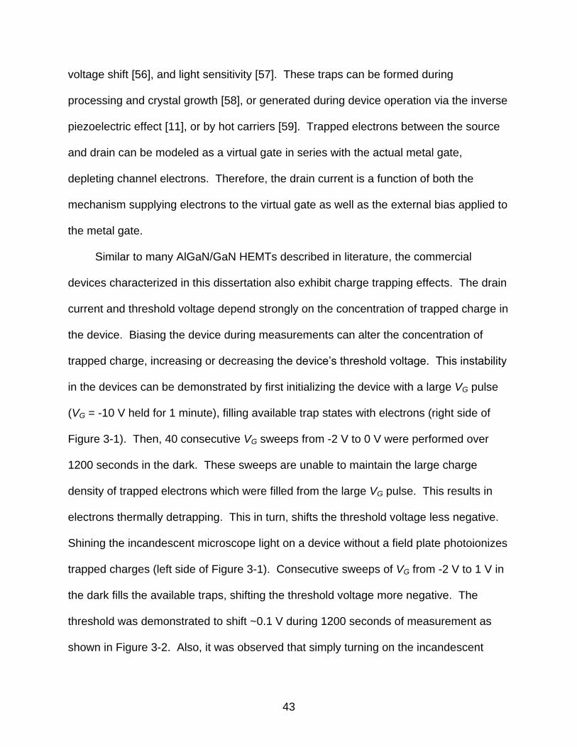
Effects of Trapped Charge ...................................................................................... 42
Experimental Setup ................................................................................................ 44
Elimination of Charge Trapping Effects ............................................................ 44
External Resistance Consideration .................................................................. 45
Results and Discussion ........................................................................................... 46
Gauge Factor Measurement ............................................................................. 46
Resistance Change with Stress ........................................................................ 47
6
2DEG Change with Stress ................................................................................ 47
Electron Mobility Change with Stress ............................................................... 48
Simulated Gauge Factor ................................................................................... 49
Summary ................................................................................................................ 49
4 VERTICAL ELECTRIC FIELD IN THE ALGAN BARRIER ...................................... 62
Introduction ............................................................................................................. 62
Ideal 1D Calculation of EAlGaN ................................................................................. 63
1D Experimentally Measured EAlGaN ....................................................................... 65
2D Simulation of EAlGaN ........................................................................................... 67
Simulation Details ............................................................................................. 67
Simulation Results ............................................................................................ 68
Summary ................................................................................................................ 69
5 FIELD DEPENDENT MECHANICAL STRESS SENSITIVITY OF ALGAN/GAN HEMT GATE LEAKAGE CURRENT ....................................................................... 84
Introduction ............................................................................................................. 84
Experiment .............................................................................................................. 85
Results and Discussion ........................................................................................... 86
Wafer Bending Results ..................................................................................... 86
Discussion ........................................................................................................ 87
Maximum compensation (r = 1) ................................................................. 90
Reduced compensation (1 < r < 2) ............................................................. 92
Reduced compensation (1 < r < 2) with reverse current ............................ 94
Summary ................................................................................................................ 96
6 CONCLUSION ...................................................................................................... 112
Overall Summary .................................................................................................. 112
Future Work .......................................................................................................... 114
LIST OF REFERENCES ............................................................................................. 116
BIOGRAPHICAL SKETCH .......................................................................................... 126
7
LIST OF TABLES
Table page 1-1 Key material parameters for high power high performance transistors ............... 23
4-1 List of parameters used in 1D EAlGaN calculation ................................................ 71
5-1 Key parameters extracted to match experimental data ...................................... 97
8
LIST OF FIGURES
Figure page 1-1 Cross-section schematic of AlGaN/GaN HEMT on Si(111) substrate. ............... 24
2-1 GaN-faced GaN crystal lattice, oriented along the <0001> direction. ................. 34
2-2 Polarizations in strained AlxGa1-xN (x = 0.26), relaxed GaN heterostructure. The strained AlGaN layer has larger spontaneous polarization than the GaN layer, as well as additional polarization from the piezoelectric effect. ................. 35
2-3 Conduction band schematic diagram of an AlGaN/GaN HEMT showing charge balance. .................................................................................................. 36
2-4 Cross-section SEM of commercial devices characterized in this dissertation. Image from Nitronex [47]. ................................................................................... 37
2-5 Typical ID-VG curve of a depletion mode AlGaN/GaN HEMT measured at VDS = 0.1 V. ............................................................................................................... 38
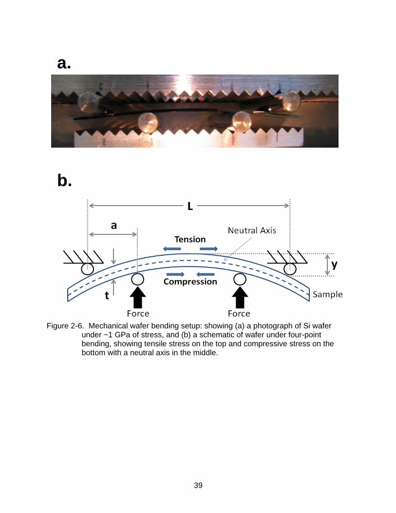
2-6 Mechanical wafer bending setup: showing (a) a photograph of Si wafer under ~1 GPa of stress, and (b) a schematic of wafer under four-point bending. ......... 39
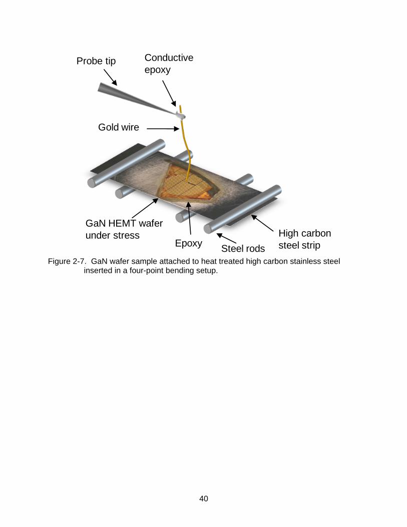
2-7 GaN wafer sample attached to heat treated high carbon stainless steel inserted in a four-point bending setup. ............................................................... 40
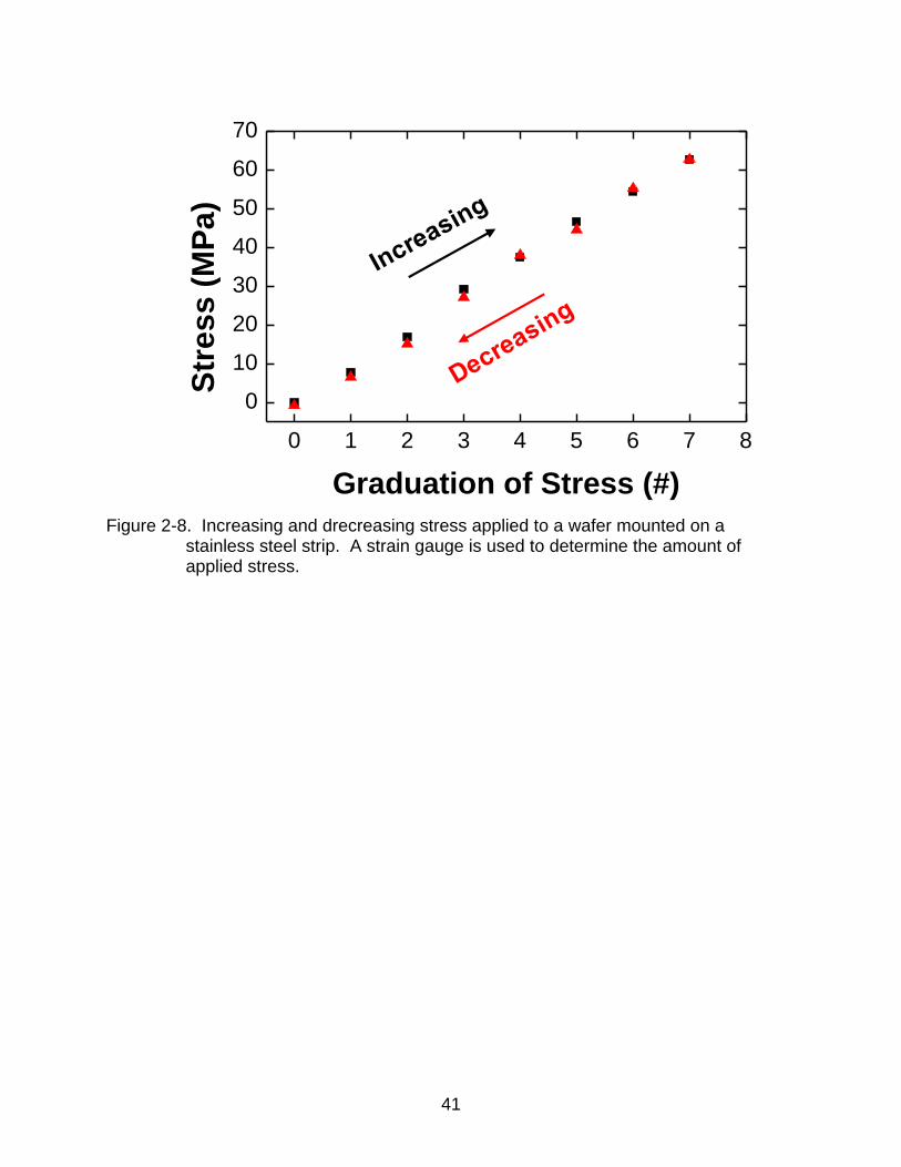
2-8 Increasing and drecreasing stress applied to a wafer mounted on a stainless steel strip. A strain gauge is used to determine the amount of applied stress. .. 41
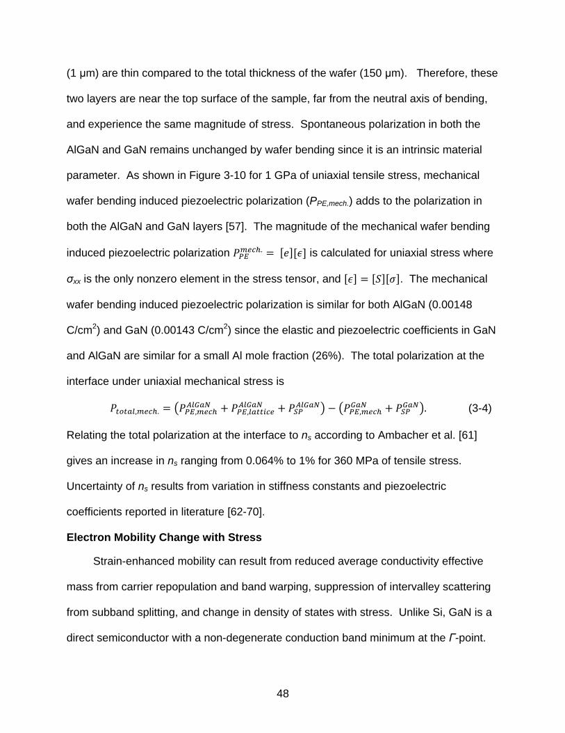
3-1 Results of consecutive VGS = -2 to 0 VDS = 0.1 V measurement sweeps resulting in charge trapping and detrapping. ...................................................... 51
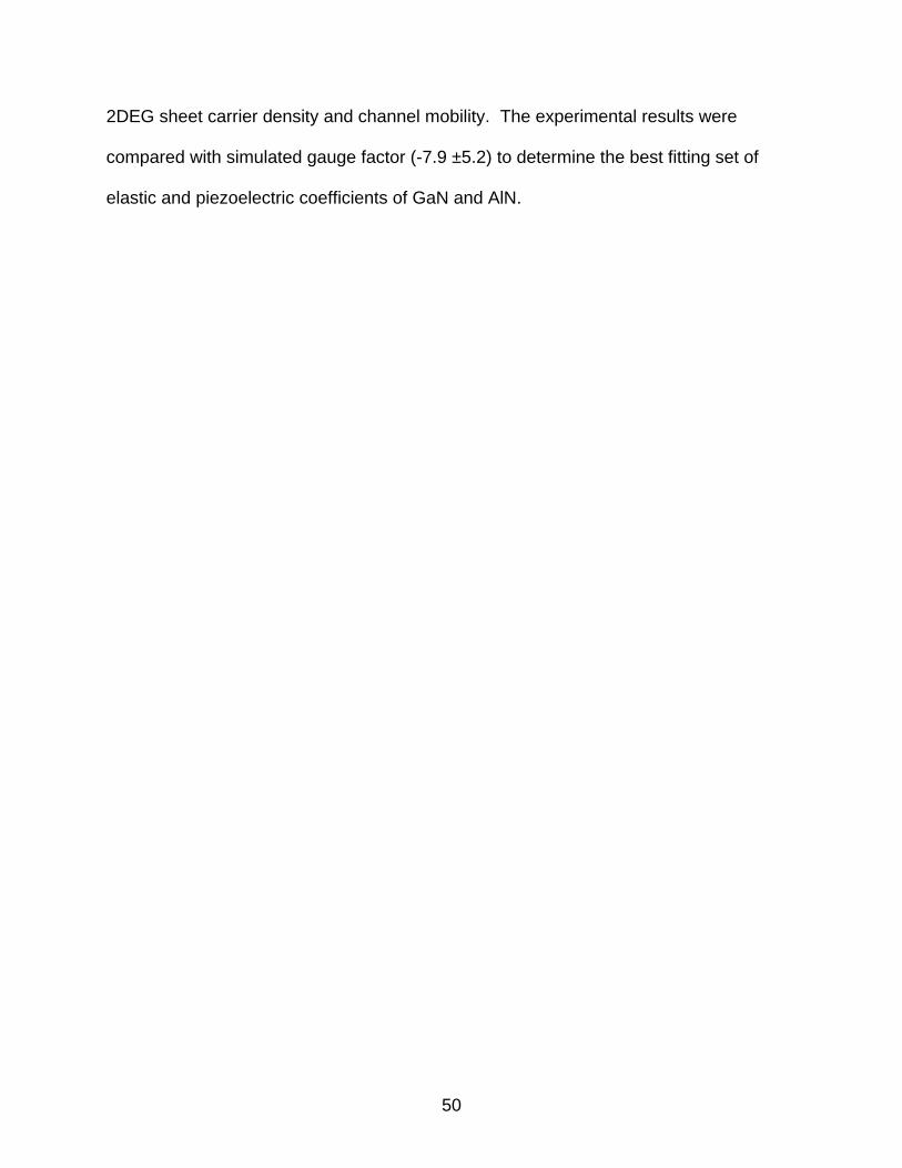
3-2 VT measured in consecutive ID – VG sweeps. In dark, |VT| can increase (decrease) from detrapping (trapping) of electrons, depending the device initialization. Under unfiltered UV illumination, VT does not fluctuate. ................ 52
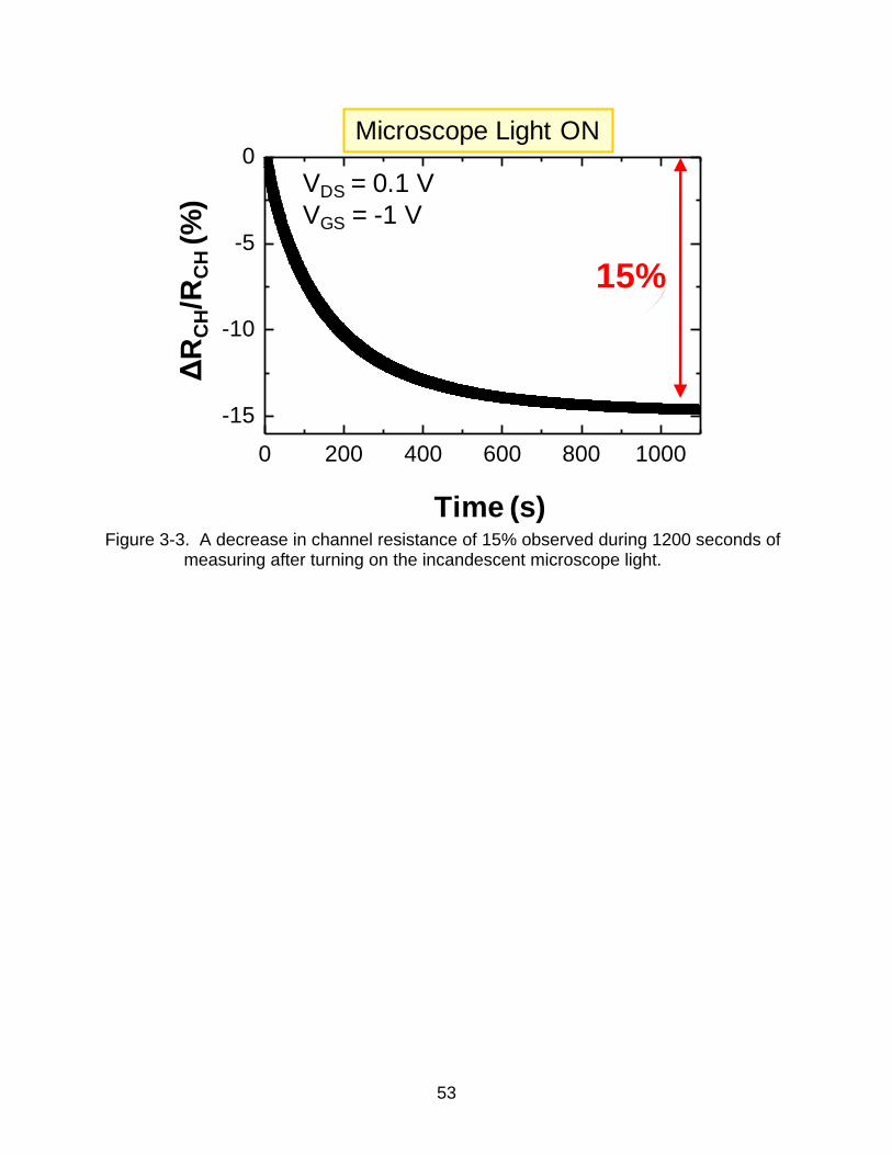
3-3 A decrease in channel resistance of 15% observed during 1200 seconds of measuring after turning on the incandescent microscope light. .......................... 53
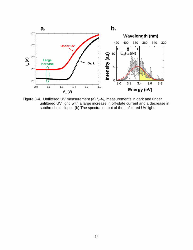
3-4 Unfiltered UV measurement (a) ID-VG measurements in dark and under unfiltered UV light with a large increase in off-state current and a decrease in subthreshold slope. (b) The spectral output of the unfiltered UV light. .............. 54
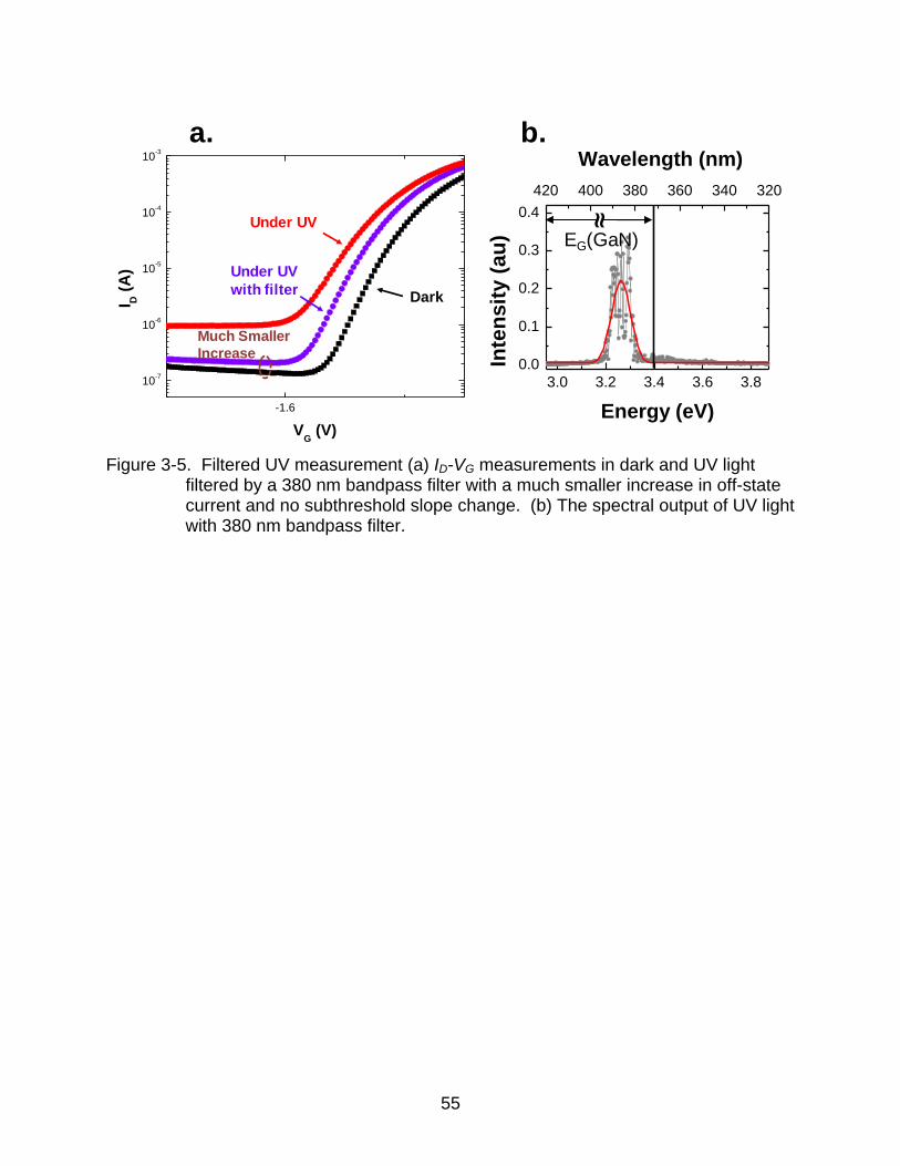
3-5 Filtered UV measurement (a) ID-VG measurements in dark and UV light filtered by a 380 nm bandpass filter. (b) The spectral output of UV light with 380 nm bandpass filter. ...................................................................................... 55
9
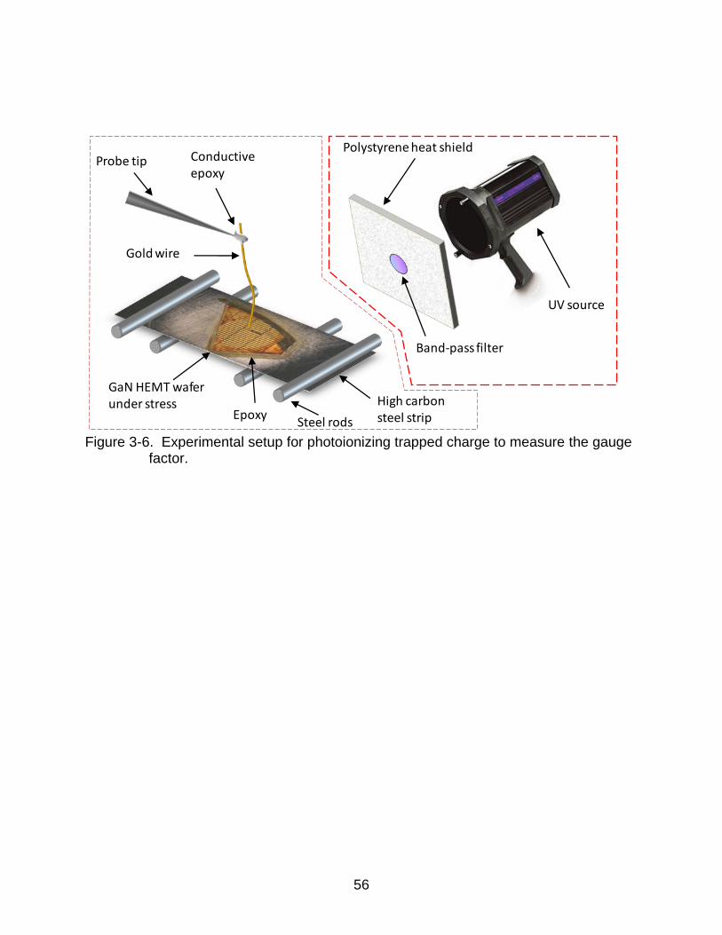
3-6 Experimental setup for photoionizing trapped charge to measure the gauge factor. ................................................................................................................. 56
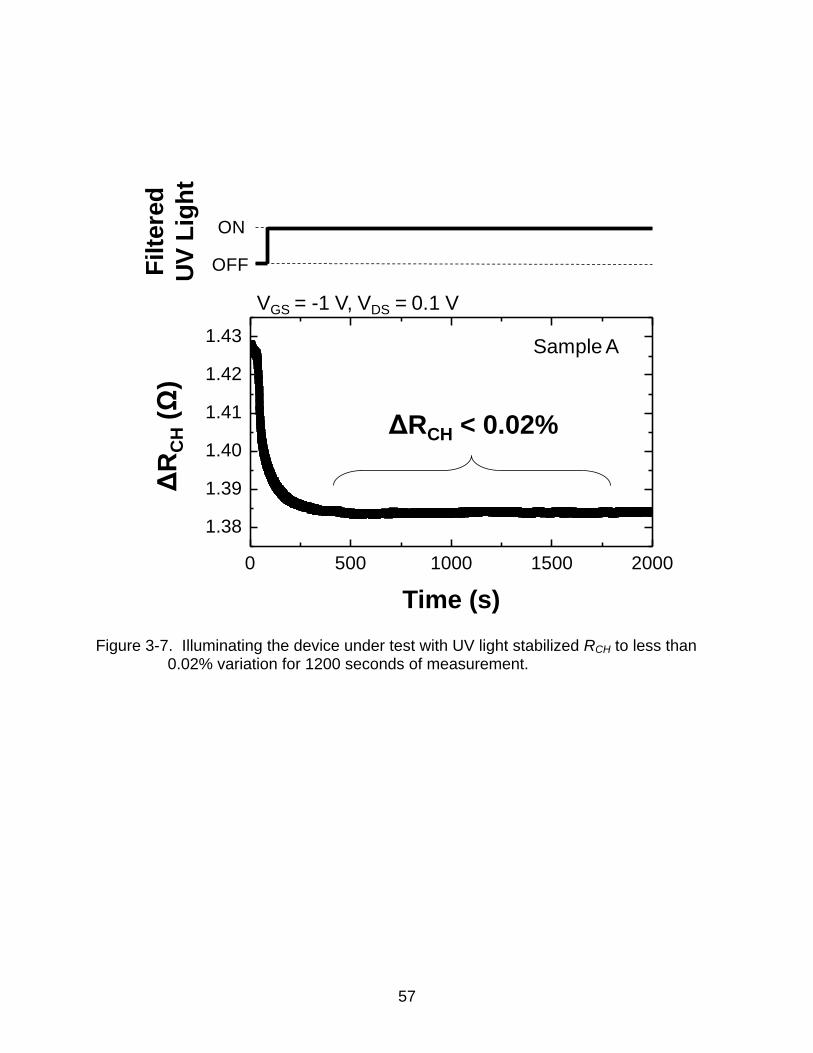
3-7 lluminating the device under test with UV light stabilized RCH to less than 0.02% variation for 1200 seconds of measurement. ........................................... 57
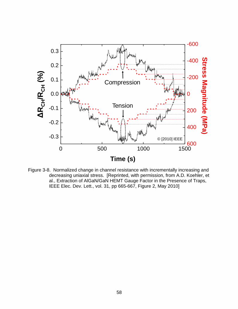
3-8 Normalized change in channel resistance with incrementally increasing and decreasing uniaxial stress. ................................................................................. 58
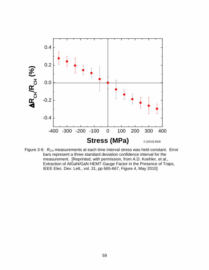
3-9 RCH measurements at each time interval stress was held constant. Error bars represent a three standard deviation confidence interval for the measurement. ..................................................................................................... 59
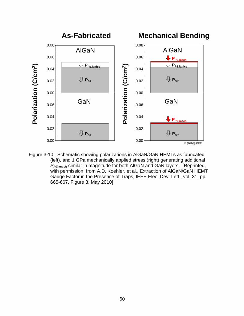
3-10 Schematic showing polarizations in AlGaN/GaN HEMTs as fabricated (left), and 1 GPa mechanically applied stress (right) generating additional PPE,mech similar in magnitude for both AlGaN and GaN layers. ........................................ 60
3-11 Simulated change in ns, μe and RCH with uniaxial stress shown in bands of uncertainty. The bands signify variations in numerical results due to uncertainty in elastic and piezoelectric coefficients. ........................................... 61
4-1 Energy band diagram schematic showing Ni/AlGaN/GaN interface ................... 72
4-2 Dependence of the 2DEG density (ns) with gate bias for the 1D case, with no interface trapped charge. Threshold is defined when ns is entirely depleted (ns = 0). ............................................................................................................... 73
4-3 Idealistic 1D calculation of EAlGaN, assuming no interface trapped charge. EAlGaN increases linearly until the threshold voltage, then saturates. .................. 74
4-4 Bar diagram of the AlGaN/GaN interface charge for an ideal device with no trapped charge and an actual device. Trapped charge reduces the positive fixed sheet charge density at the AlGaN/GaN interface. .................................... 75
4-5 Capacitance-Voltage measurement, which is integrated in order to determine ns(V). .................................................................................................................. 76
4-6 1D ideal (no interface trapped charge) calculation and the experimental result from experimental parameters obtained by adjusting σint and obtaining ns from C-V ............................................................................................................. 77
4-7 Optimized grid for Sentaurus simulation of the AlGaN/GaN HEMT device. ........ 78
4-8 Experimental calculation of EAlGaN versus VG compared to 2D simulation results. ................................................................................................................ 79
4-9 Vertical cross-section of electric field of the AlGaN/GaN HEMT at the (a) center of the gate and (b) drain edge of the gate................................................ 80
10
4-10 Horizontal cross-section of EAlGaN taken near the top surface of the AlGaN barrier 1 nm below the gate contact. .................................................................. 81
4-11 Horizontal cross-section of the electrostatic potential taken near the top surface of the GaN 0.5 nm below the AlGaN/GaN interface. .............................. 82
4-12 Horizontal component of EAlGaN at the (a) center and (b) edge of the gate. ........ 83
5-1 Electrical step stress measurement showing the breakdown of JG at the critical voltage. .................................................................................................... 98
5-2 Normalized change in JG for incrementally increasing and decreasing uniaxial stress for (a) VG = -0.25 V and (b) VG = -4 V. ........................................ 99
5-3 ΔJG(σ)/JG(0) averaged for all levels of compressive and tensile stress at VG = -0.25 V and -4 V. Uncertainty comes from three standard deviation from the measurement of ΔJG(σ)/JG(0) over the duration stress was held constant. 100
5-4 Experimentally measured stress sensitivity of JG per 100 MPa of stress, as a function of reverse gate bias. ............................................................................ 101
5-5 Measured gate leakage current density versus gate voltage from T = 300 K to 400 K for unstressed AlGaN/GaN HEMT...................................................... 102
5-6 PF plot showing linear fit to the measured data for T = 300 K to 400 K. ........... 103
5-7 The slope of the PF plot (m) plotted versus 1/T. The slope of this plot (m’) is
used to calculate . ................................................................................. 104
5-8 The y-intercept of the PF plot versus 1/T. The slope of this plot (m’’) is used to calculate the trap energy level. ..................................................................... 105
5-9 Schematic of change in EA with compressive and tensile stress. Compressive stress increases EA, decreasing r, increasing compensation, and reducing PF emission. The opposite is true for tensile stress. .................. 106
5-10 Simulated stress sensitivity of JG per 100 MPa of stress, including EA and r changing with stress, as a function of reverse gate bias. ................................. 107
5-11 Schematic of JG, JPF, and JR assuming JR is a bulk-assisted mechanism driven by the PF emission current for VG = -2 V and other parameters from Table 4-1. ......................................................................................................... 108
5-12 Measured JG, ideal JPF obtained by linear extrapolation of the linear PF fit, and JR calculated by the difference between JPF and JG. .................................. 109
11
5-13 Simulated stress sensitivity of JG at 100 MPa of stress, including JR, as a function of reverse gate bias. JR not changing with stress overestimates the stress sensitivity. However, ΔJR(σ)/JG(0) = 1.5% matches experiment. ........... 110
5-14 Energy band diagrams showing the reduction in the AlGaN barrier thickness at the gate edges for VG well below VT. ............................................................ 111

12
LIST OF ABBREVIATIONS
DC Direct current
FN Fowler-Nordheim
GF Gauge factor
HEMT High electron mobility transistor
MEMS Microelectromechanical systems
MOCVD Metal organic chemical vapor deposition
MOSFET Metal oxide semiconductor field effect transistor
PF Poole-Frenkel
SEM Scanning electron microscope
UV Ultraviolet
13
Abstract of Dissertation Presented to the Graduate School of the University of Florida in Partial Fulfillment of the Requirements for the Degree of Doctor of Philosophy
IMPACT OF MECHANICAL STRESS ON ALGAN/GAN HEMT PERFORMANCE:
CHANNEL RESISTANCE AND GATE CURRENT
By
Andrew Daniel Koehler
December 2011
Chair: Scott E. Thompson Cochair: Toshikazu Nishida Major: Electrical and Computer Engineering
AlGaN/GaN high electron mobility transistors (HEMTs) stand out with superb
advantages for high-power, high-temperature, high-frequency applications. Internal
stress is inherent to state-of-the-art AlGaN/GaN HEMTs and has the potential to impact
performance and reliability. Strain is an integral part of modern semiconductor
technology and has been used to extend scaling of Si for nearly a decade, and the
performance and reliability implications are well understood. Understanding the impact
of mechanical stress on AlGaN/GaN HEMT channel resistance and gate current is
crucial for continued improvements in device performance and reliability.
Repeatable gauge factors of an AlGaN/GaN HEMT device were obtained after
eliminating parasitic charge trapping effects. Over four orders of magnitude of variation
in gauge factors are reported in literature. Charge traps are likely responsible for the
huge discrepancy. By employing continuous sub-bandgap optical excitation, the effect
of non-repeatable charge trapping transients was effectively minimized, allowing the
gauge factor to be accurately measured. The measured gauge factor is compared to a
14
simulated gauge factor, calculated from stress-induced changes in the 2DEG sheet
carrier density and mobility.
Stress-altered gate leakage currents in AlGaN/GaN HEMTs are measured as a
function of constant applied reverse gate bias. Increasing reverse gate bias decreases
the stress sensitivity of the gate leakage current. Poole-Frenkel emission dominates the
gate leakage current for gate biases above threshold. Stress changes Poole-Frenkel
emission by altering the trap activation energy, which also changes the compensation
parameter. Reverse tunneling current which balances the forward Poole-Frenkel
current at equilibrium is modeled to explain the experimental results. Tensile
(compressive) stress decreases (increases) the trap activation energy, increasing
(decreasing) the gate leakage current. Although below threshold, the electric field in the
AlGaN barrier saturates in the middle of the gate, the electric field increases at the gate
edges because of two-dimensional effects. For larger reverse gate bias much below
threshold, the thickness of the AlGaN tunneling barrier decreases which causes Fowler-
Nordheim tunneling at the gate edges to dominate the current transport.
15
CHAPTER 1 INTRODUCTION AND OVERVIEW
Overview of AlGaN/GaN HEMTs
III-V semiconductor devices show promise over Si metal-oxide-semiconductor
field-effect transistors (MOSFETs) for high speed circuits. The focus of early III-V
semiconductor research was toward GaAs MOSFET technology, however poor quality
native oxide and high surface state density prevented channel electron accumulation.
In 1980, Takashi Mimura from Fujitsu Laboratories developed a depletion-mode high
electron mobility transistor (HEMT) with selectively doped n-type AlGaAs barrier,
eliminating issues associated with native oxides on GaAs [1][2]. Although AlxGa1-xN
was historically used in optoelectronic devices because of its direct and tunable band
gap, AlGaN/GaN HEMTs were developed in 1993 by M. Asif Khan of APA Optics for
high temperature, high performance devices [3].
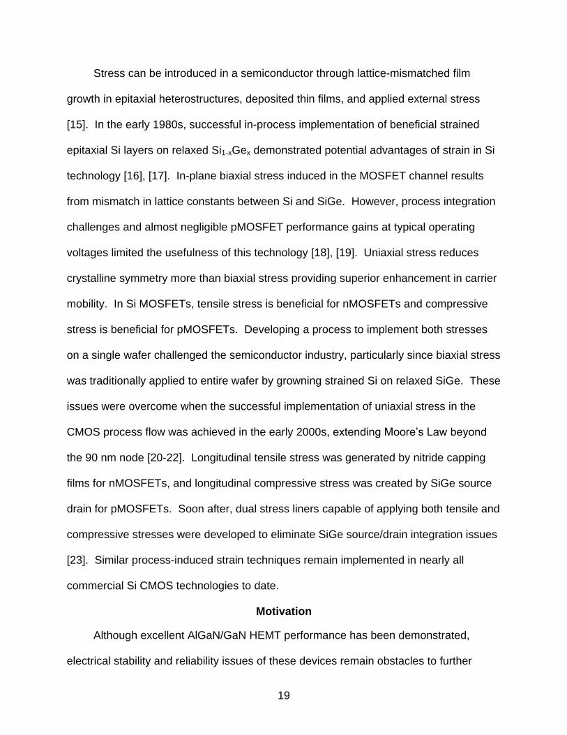
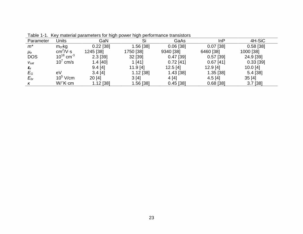
Unique advantages associated with GaN make AlGaN/GaN HEMTs desirable for
high-speed, high-performance applications. Table 1-1 summarizes key material
parameters for high power high performance devices, displaying benefits of GaN
compared to other relevant semiconductors. Although the effective mass (m*) of GaN is
larger than GaAs and InP, resulting in lower bulk effective low-field electron mobility
(μe), the high conduction band density of states (DOS) and large saturation velocity (vsat)
still permits large current densities. The low dielectric constant ( ) reduces capacitive
loading and allows for large area devices, increasing RF current and power [4]. The
large band gap (EG) improves radiation resistance, results in high intrinsic temperature,
and provides a very large breakdown field (Ebr) necessary for handling high RF power.
16
Heat dissipation benefits from the high thermal conductivity (κ), allowing for more
efficient dissipation of heat away from the device.
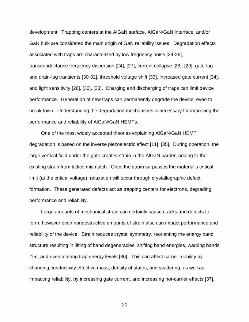
Mechanical strain resulting from lattice mismatch between the AlGaN and GaN
layers induces piezoelectric polarization. This polarization increases the two-
dimensional electron gas (2DEG) sheet carrier density (ns). Benefitting from
mechanical strain, AlGaN/GaN HEMTs are capable of achieving ns greater than 1013
cm-2, without intentional doping. This is significantly higher than other III-V systems due
to strong piezoelectric polarization in the Wurtzite GaN and AlN. Biaxial tensile stress in
the AlGaN barrier results from the lattice mismatch between AlGaN and GaN, increase
polarization at the AlGaN/GaN interface and induces the mobile 2DEG. A cross-section
schematic of an AlGaN/GaN HEMT is shown in Figure 1-1.
The combination of material and structural benefits allows AlGaN/GaN HEMTs to
be suitable for various high power, high performance circuits. AlGaN/GaN HEMTs are
attractive for expanding markets in communications, radar, sensors, and automotive for
both military and commercial applications. Integration of GaN on Si(111) substrates
improves device performance and reliability while reducing cost [5], making AlGaN/GaN
HEMT technology extremely attractive for commercial and military markets. Currently,
several commercial vendors have AlGaN/GaN HEMT devices available, such as Cree,
Fujitsu, Nitronex, RFMD, Toshiba, and Triquint.
An example AlGaN/GaN HEMT power transistors of current commercially
availableoperate at 2.7 to 3.5 GHz range (S-band) ,outputting 240 W of power with a
power-added efficiency (PAE) of 60% [6][7]. In academia, an example of the current
devices under investigation include Al2O3 dielectric layers forming metal-oxide-

17
semiconductor HEMTs, providing transistors with a PAE of 73% at 4 GHz at a 45 V
drain bias [8].
Stress in AlGaN/GaN HEMTs
Stress is an integral part of AlGaN/GaN HEMT devices. Large mechanical stress
profiles are created during processing and are generated during operation. These
stresses can impact device performance and reliability.
In order for AlGaN/GaN HEMTs to be commercially competitive with Si
alternatives, low-cost, large-scale production must be achieved. Si(111) substrates
offer advantages of low-cost, large size, and high quality over sapphire and SiC
alternatives. However, large differences in lattice constants (~17%) and thermal
expansion coefficients (TEC) (~56%) between GaN and the Si(111) produce large
strains, resulting in the formation of crystallographic defects [5]. High quality GaN
layers on Si, free of cracks and dislocations, have been fabricated through
implementation of stress mitigation using transition layers [5]. It is hypothesized that the
lattice mismatch stress is primarily absorbed by the Al/Si interface, while the (Al, Ga) N
transition layer absorbs the TEC mismatch stress, which occurs during processing [5].
Another type of stress induced during processing is biaxial tensile stress in the
AlGaN barrier layer. The AlGaN barrier is pseudomorphically grown on the relaxed
GaN channel/buffer. Lattice mismatch between AlGaN and GaN induces a biaxial
tensile stress in the AlGaN barrier. For an Al concentration of 26%, the AlGaN barrier
has ~3 GPa of biaxial tensile stress induced. This stress is advantageous since
Wurtzite GaN and AlN grown in the (0001) orientation are both strongly piezoelectric [9].
The piezoelectric effect results in a polarization fixed charge at the AlGaN/GaN
interface, inducing a mobile sheet charge layer which is termed a two-dimensional
18
electron gas (2DEG). SiO2 or Si3N4 passivation possess residual stress which also has
been shown to induce stress, adding to the lattice mismatch stress and increasing the
2DEG [10].
During operation, the vertical electric field under the gate contact through the
inverse piezoelectric effect induces additional stress in the AlGaN barrier. This vertical
field is the largest at the gate edges, where significant amounts of stress (500 MPa) can
be generated in the AlGaN barrier during normal operation (VGS = 30 V). It has been
proposed that stress generated from the inverse piezoelectric effect can initiate defect
formation leading to irreversible degradation [11]. Stress is of particular importance to
performance and reliability of AlGaN/GaN HEMTs and has been investigated
extensively in Si MOSFET technology for improving performance.
Stress in Semiconductor Technology
Piezoresistance, or change in electrical resistance in the presence of external
mechanical stress, was first discovered in copper wires by Lord Kelvin in 1856 and first
utilized in strain gauges in the 1930s [12]. Twenty years later, theory was developed
outlining the implications of stress on semiconductors based on energy shifts resulting
from deformation of the crystal lattice by Bardeen and Shockley [13]. In 1954, the first
piezoresistance measurements of n and p type conduction for both Si and Ge were
published [14]. The piezoresistive property of Si gave potential for Si pressure, flow,
force, and acceleration sensors, as well as reducing the channel resistance of Si
MOSFETs. In semiconductors, strain alters crystal symmetry and then alters the
energy band structure by shifting bands, lifting band degeneracies, and warping bands.
As a result, strain alters the carrier’s mobility through mass change and of scattering
change.
19
Stress can be introduced in a semiconductor through lattice-mismatched film
growth in epitaxial heterostructures, deposited thin films, and applied external stress
[15]. In the early 1980s, successful in-process implementation of beneficial strained
epitaxial Si layers on relaxed Si1-xGex demonstrated potential advantages of strain in Si
technology [16], [17]. In-plane biaxial stress induced in the MOSFET channel results
from mismatch in lattice constants between Si and SiGe. However, process integration
challenges and almost negligible pMOSFET performance gains at typical operating
voltages limited the usefulness of this technology [18], [19]. Uniaxial stress reduces
crystalline symmetry more than biaxial stress providing superior enhancement in carrier
mobility. In Si MOSFETs, tensile stress is beneficial for nMOSFETs and compressive
stress is beneficial for pMOSFETs. Developing a process to implement both stresses
on a single wafer challenged the semiconductor industry, particularly since biaxial stress
was traditionally applied to entire wafer by growning strained Si on relaxed SiGe. These
issues were overcome when the successful implementation of uniaxial stress in the
CMOS process flow was achieved in the early 2000s, extending Moore’s Law beyond
the 90 nm node [20-22]. Longitudinal tensile stress was generated by nitride capping
films for nMOSFETs, and longitudinal compressive stress was created by SiGe source
drain for pMOSFETs. Soon after, dual stress liners capable of applying both tensile and
compressive stresses were developed to eliminate SiGe source/drain integration issues
[23]. Similar process-induced strain techniques remain implemented in nearly all
commercial Si CMOS technologies to date.
Motivation
Although excellent AlGaN/GaN HEMT performance has been demonstrated,
electrical stability and reliability issues of these devices remain obstacles to further
20
development. Trapping centers at the AlGaN surface, AlGaN/GaN interface, and/or
GaN bulk are considered the main origin of GaN reliability issues. Degradation effects
associated with traps are characterized by low frequency noise [24-26],
transconductance frequency dispersion [24], [27], current collapse [28], [29], gate-lag
and drain-lag transients [30-32], threshold voltage shift [33], increased gate current [34],
and light sensitivity [28], [30], [33]. Charging and discharging of traps can limit device
performance. Generation of new traps can permanently degrade the device, even to
breakdown. Understanding the degradation mechanisms is necessary for improving the
performance and reliability of AlGaN/GaN HEMTs.
One of the most widely accepted theories explaining AlGaN/GaN HEMT
degradation is based on the inverse piezoelectric effect [11], [35]. During operation, the
large vertical field under the gate creates strain in the AlGaN barrier, adding to the
existing strain from lattice mismatch. Once the strain surpasses the material’s critical
limit (at the critical voltage), relaxation will occur through crystallographic defect
formation. These generated defects act as trapping centers for electrons, degrading
performance and reliability.
Large amounts of mechanical strain can certainly cause cracks and defects to
form, however even nondestructive amounts of strain also can impact performance and
reliability of the device. Strain reduces crystal symmetry, reorienting the energy band
structure resulting in lifting of band degeneracies, shifting band energies, warping bands
[15], and even altering trap energy levels [36]. This can affect carrier mobility by
changing conductivity effective mass, density of states, and scattering, as well as
impacting reliability, by increasing gate current, and increasing hot-carrier effects [37].

21
Since stress is a major factor in the operation, performance, and reliability in
AlGaN/GaN HEMT devices, a thorough understanding of the impact of stress on
performance and reliability can lead to improvements in device design. The effects of
strain in Si MOSFETs are well understood and used to improve the devices.
Mechanical wafer bending is a cost-effective method to study the effects of stress on
semiconductor devices which has been extensively used to isolate and study the effect
of stress in Si MOSFETs. A systematic study of the effects of externally applied
mechanical stress on the AlGaN/GaN HEMT channel resistance and gate current can
provide insights into the physical mechanisms responsible for stress-related
performance and reliability issues.
Organization
The focus of this dissertation is to provide an improved understanding of the
impact of mechanical stress on AlGaN/GaN HEMT channel resistance and gate current
which are key parameters for studying performance and reliability. Previous studies
have suggested that catastrophic failure can be related to stress [11], [35]. Combining
systematic mechanical wafer bending experiments and theory, physical models are
presented to explain the incremental effect of stress on channel resistance and gate
leakage current.
Background information will be provided in Chapter 2, beginning with
fundamentals of AlGaN/GaN HEMT operation. Then, a brief description of the
characterization method is provided, followed by details on mechanical wafer bending.
Chapter 3 presents experimental and theoretical details on the extraction of the
AlGaN/GaN HEMT gauge factor in the presence of traps. A comprehensive
investigation of the vertical electric field in the AlGaN barrier is given in Chapter 4. The

22
electric field model and simulation results assist in the analysis of the effect of stress on
the gate leakage current presented in Chapter 5. Chapter 6 concludes the study with
an overall summary and suggestions for future work.
23
Table 1-1. Key material parameters for high power high performance transistors
Parameter Units GaN Si GaAs InP 4H-SiC
m* m0*kg 0.22 [38] 1.56 [38] 0.06 [38] 0.07 [38] 0.58 [38] μe cm2/V·s 1245 [38] 1750 [38] 9340 [38] 6460 [38] 1000 [38] DOS 1018 cm-3 2.3 [39] 32 [39] 0.47 [39] 0.57 [39] 24.9 [39] vsat 107 cm/s 1.4 [40] 1 [41] 0.72 [41] 0.67 [41] 0.33 [39] εr 9.4 [4] 11.9 [4] 12.5 [4] 12.9 [4] 10.0 [4] EG eV 3.4 [4] 1.12 [38] 1.43 [38] 1.35 [38] 5.4 [38] Ebr 105 V/cm 20 [4] 3 [4] 4 [4] 4.5 [4] 35 [4] κ W/˚K·cm 1.12 [38] 1.56 [38] 0.45 [38] 0.68 [38] 3.7 [38]
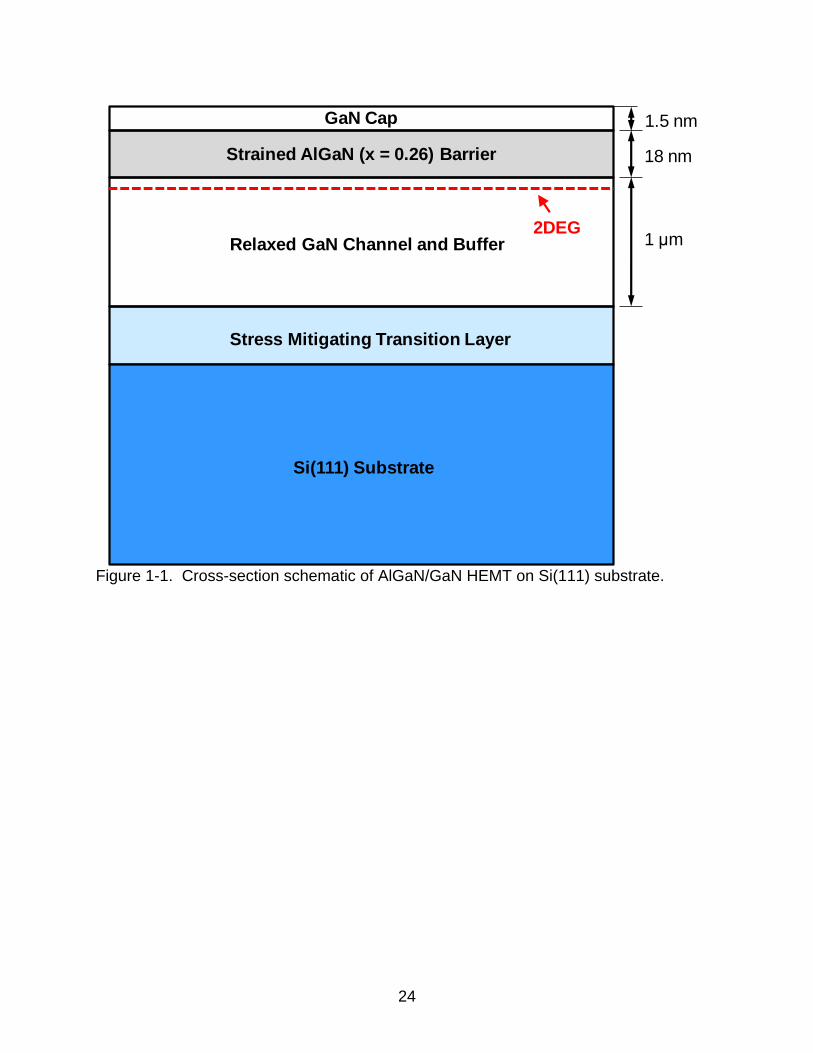
24
Figure 1-1. Cross-section schematic of AlGaN/GaN HEMT on Si(111) substrate.
Si(111) Substrate
Stress Mitigating Transition Layer
Relaxed GaN Channel and Buffer
Strained AlGaN (x = 0.26) Barrier
GaN Cap
2DEG
1.5 nm
18 nm
1 μm
25
CHAPTER 2
ALGAN/GAN HEMT AND WAFER BENDING BACKGROUND
GaN Fundamentals
AlGaN/GaN HEMTs are depletion mode field effect transistors, benefiting from
large 2DEG sheet carrier density, obtained without intentional doping or applied gate
bias. The combination of spontaneous polarization (PSP) and piezoelectric polarization
(PPE) in the AlGaN and GaN layers create a macroscopic polarization which induces a
2DEG in the absence of electric field and intentional doping.
Spontaneous Polarization
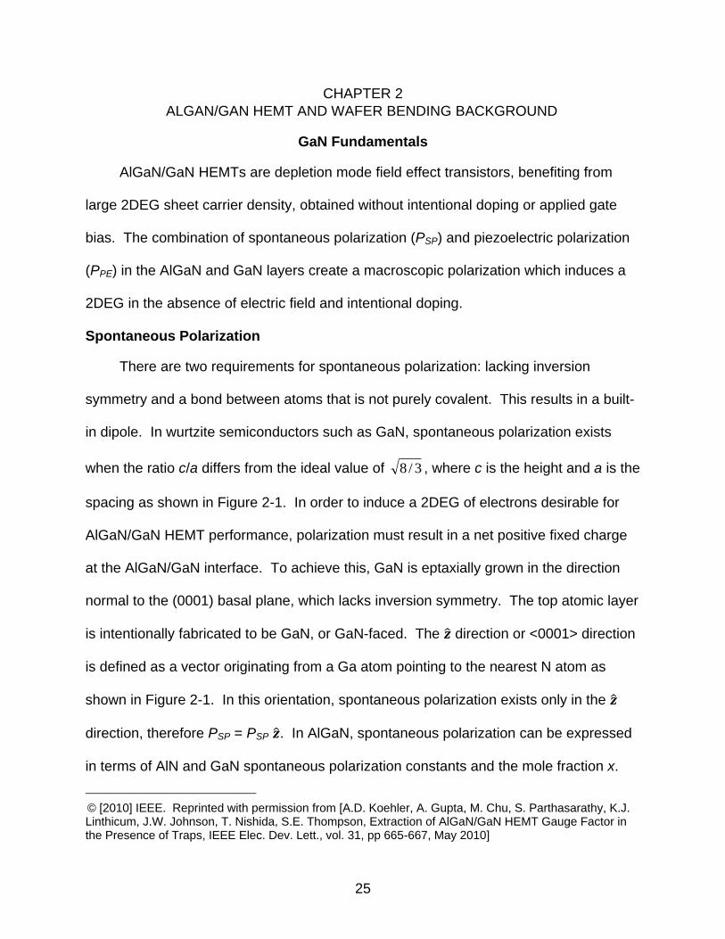
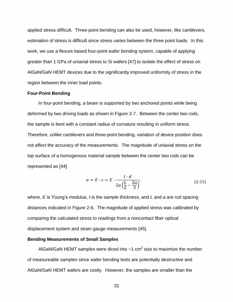
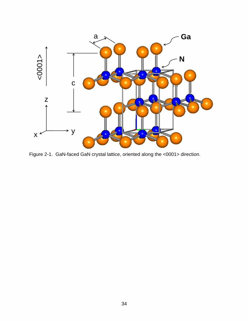
There are two requirements for spontaneous polarization: lacking inversion
symmetry and a bond between atoms that is not purely covalent. This results in a built-
in dipole. In wurtzite semiconductors such as GaN, spontaneous polarization exists
when the ratio c/a differs from the ideal value of 3/8 , where c is the height and a is the
spacing as shown in Figure 2-1. In order to induce a 2DEG of electrons desirable for
AlGaN/GaN HEMT performance, polarization must result in a net positive fixed charge
at the AlGaN/GaN interface. To achieve this, GaN is eptaxially grown in the direction
normal to the (0001) basal plane, which lacks inversion symmetry. The top atomic layer
is intentionally fabricated to be GaN, or GaN-faced. The ̂ direction or <0001> direction
is defined as a vector originating from a Ga atom pointing to the nearest N atom as
shown in Figure 2-1. In this orientation, spontaneous polarization exists only in the ̂
direction, therefore PSP = PSP ̂. In AlGaN, spontaneous polarization can be expressed
in terms of AlN and GaN spontaneous polarization constants and the mole fraction x.
© [2010] IEEE. Reprinted with permission from [A.D. Koehler, A. Gupta, M. Chu, S. Parthasarathy, K.J. Linthicum, J.W. Johnson, T. Nishida, S.E. Thompson, Extraction of AlGaN/GaN HEMT Gauge Factor in the Presence of Traps, IEEE Elec. Dev. Lett., vol. 31, pp 665-667, May 2010]
26
( )
( ) (2-1)
It is important to note that spontaneous polarization in AlN ( -0.081 C/m2) is
larger than in GaN ( -0.029 C/m2) [9].
Piezoelectric Polarization
A crystal which becomes electrically polarized in the presence of applied
mechanical stress is described as piezoelectric. Piezoelectric polarization is observed
in crystals lacking a center of inversion, such as GaN and AlGaN. Piezoelectric
polarization is described by the piezoelectric tensor [e] and strain tensor
. (2-2)
The piezoelectric tensor is a 3 x 6 matrix and the strain vector can be written with
six dimensional components. In wurtite GaN, the piezoelectric polarization is given by,
[
] [
]
[
]
. (2-3)
In the case of an AlGaN/GaN HEMT, the GaN layer is significantly thicker relative
to the AlGaN barrier layer, so the AlGaN barrier strains to lattice match the relaxed GaN
layer. Strain which is generated from this lattice mismatch is in the out-of-plane
direction (along the c-axis) defined by the lattice distortion as ( ) . Also, an
isotropic in-plane strain results, where ( ) , where a and c are the
strained and a0 and c0 are the unstrained lattice constants. The polarization induced by
lattice mismatch strain in AlGaN/GaN HEMT devices grown along the <0001> direction
only exists in the <0001> direction. Therefore, the piezoelectric polarization resulting

27
from lattice mismatch strain in the AlGaN layer of an AlGaN/GaN HEMT can be
expressed as:
( ). (2-4)
Stress [σ] and can be related by Hooke’s law, where,
, (2-5)
and analogously
(2-6)
The stiffness tensor [C] and compliance tensor [S] = [C]-1 are 6x6 element tensors
of the following form for hexagonal symmetry
[ ]
(2-7)
[ ]
(2-8)
The polarization resulting from built-in lattice mismatch stress in the AlGaN layer of
an AlGaN/GaN HEMT can be simplified in terms of atomic distortion, piezoelectric
constants, and stiffness constants, giving
(
) (2-9)
28
Formation of 2DEG
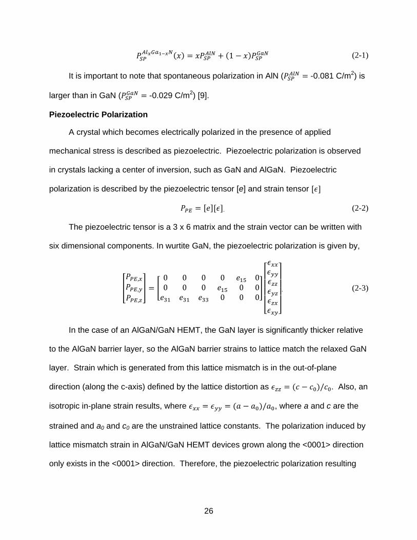
The net positive fixed sheet charge at the AlGaN/GaN heterostructure interface
(σint) results from the polarization difference between AlGaN and GaN, which induces
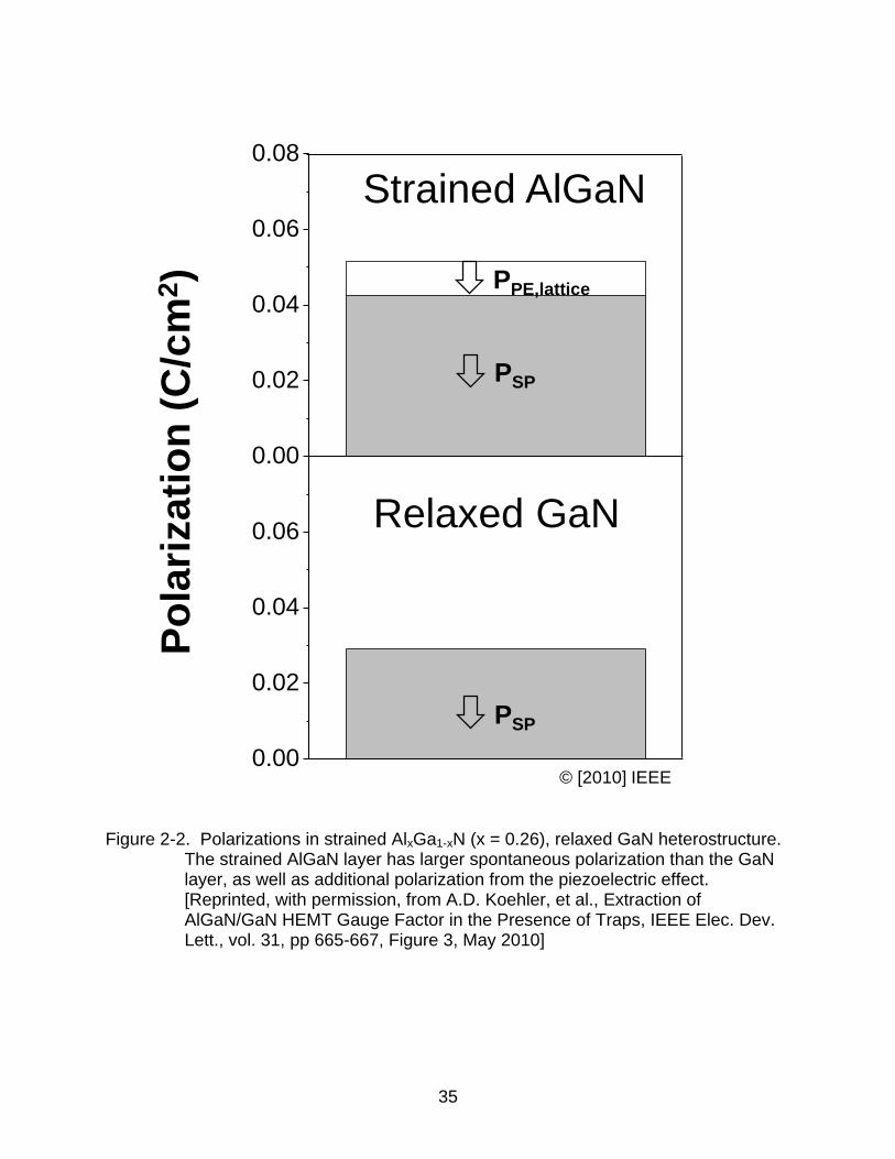
the mobile 2DEG. Figure 2-2 shows a plot of the polarizations for a strained AlxGa1-xN
(x = 0.26) layer on relaxed GaN. The spontaneous polarization in AlGaN and GaN, as
well as the piezoelectric polarizations in the AlGaN layer, are oriented downward,
toward the substrate. The sum of spontaneous and piezoelectric polarizations, or the
total polarization in the AlGaN layer ( ) is larger than the total polarizations in GaN
( ). The net polarization (σPZ =
) is equivalent to a positive fixed
sheet charge density at the AlGaN/GaN interface. In a device with interface trapped
charge (Qit), the interface sheet charge is reduced by Qit,
(
) . (2-10)
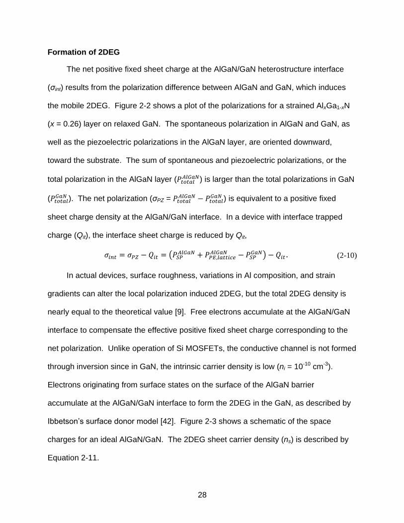
In actual devices, surface roughness, variations in Al composition, and strain
gradients can alter the local polarization induced 2DEG, but the total 2DEG density is
nearly equal to the theoretical value [9]. Free electrons accumulate at the AlGaN/GaN
interface to compensate the effective positive fixed sheet charge corresponding to the
net polarization. Unlike operation of Si MOSFETs, the conductive channel is not formed
through inversion since in GaN, the intrinsic carrier density is low (ni = 10-10 cm-3).
Electrons originating from surface states on the surface of the AlGaN barrier
accumulate at the AlGaN/GaN interface to form the 2DEG in the GaN, as described by
Ibbetson’s surface donor model [42]. Figure 2-3 shows a schematic of the space
charges for an ideal AlGaN/GaN. The 2DEG sheet carrier density (ns) is described by
Equation 2-11.
29
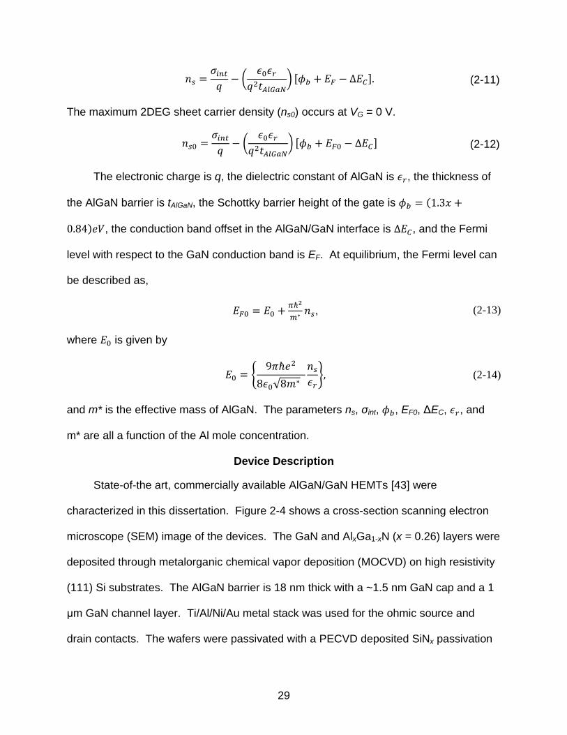
(
) (2-11)
The maximum 2DEG sheet carrier density (ns0) occurs at VG = 0 V.
(
) (2-12)
The electronic charge is q, the dielectric constant of AlGaN is , the thickness of
the AlGaN barrier is tAlGaN, the Schottky barrier height of the gate is (
) , the conduction band offset in the AlGaN/GaN interface is , and the Fermi
level with respect to the GaN conduction band is EF. At equilibrium, the Fermi level can
be described as,
, (2-13)
where is given by
,
√
- (2-14)
and m* is the effective mass of AlGaN. The parameters ns, σint, , EF0, ΔEC, , and
m* are all a function of the Al mole concentration.
Device Description
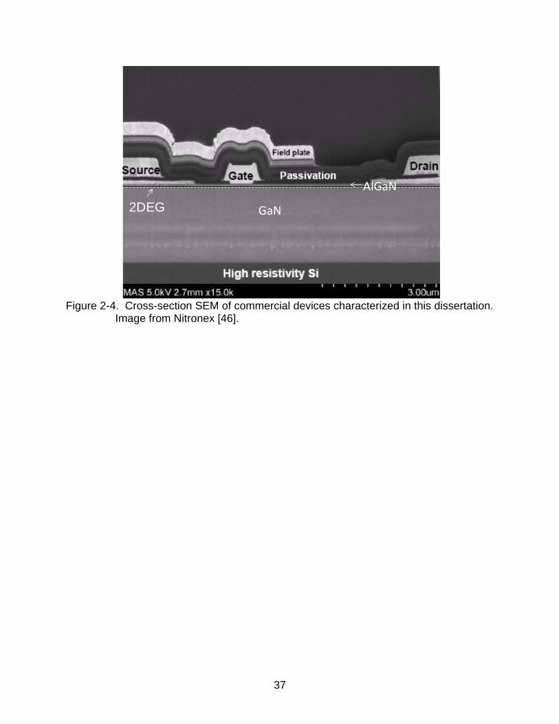
State-of-the art, commercially available AlGaN/GaN HEMTs [43] were
characterized in this dissertation. Figure 2-4 shows a cross-section scanning electron
microscope (SEM) image of the devices. The GaN and AlxGa1-xN (x = 0.26) layers were
deposited through metalorganic chemical vapor deposition (MOCVD) on high resistivity
(111) Si substrates. The AlGaN barrier is 18 nm thick with a ~1.5 nm GaN cap and a 1
μm GaN channel layer. Ti/Al/Ni/Au metal stack was used for the ohmic source and
drain contacts. The wafers were passivated with a PECVD deposited SiNx passivation

30
layer. In a separate lithography step, Ni/Au Schottky gates were formed. Gate-to-
source spacing of 1.0 μm, gate lengths of 0.5 μm and 1 μm, and gate-drain spacing of
3.2 μm, gives a total channel length of 4.7 μm. The channel width is 50 μm. The
substrate was thinned to a thickness of 150 μm using standard Si grinding techniques.
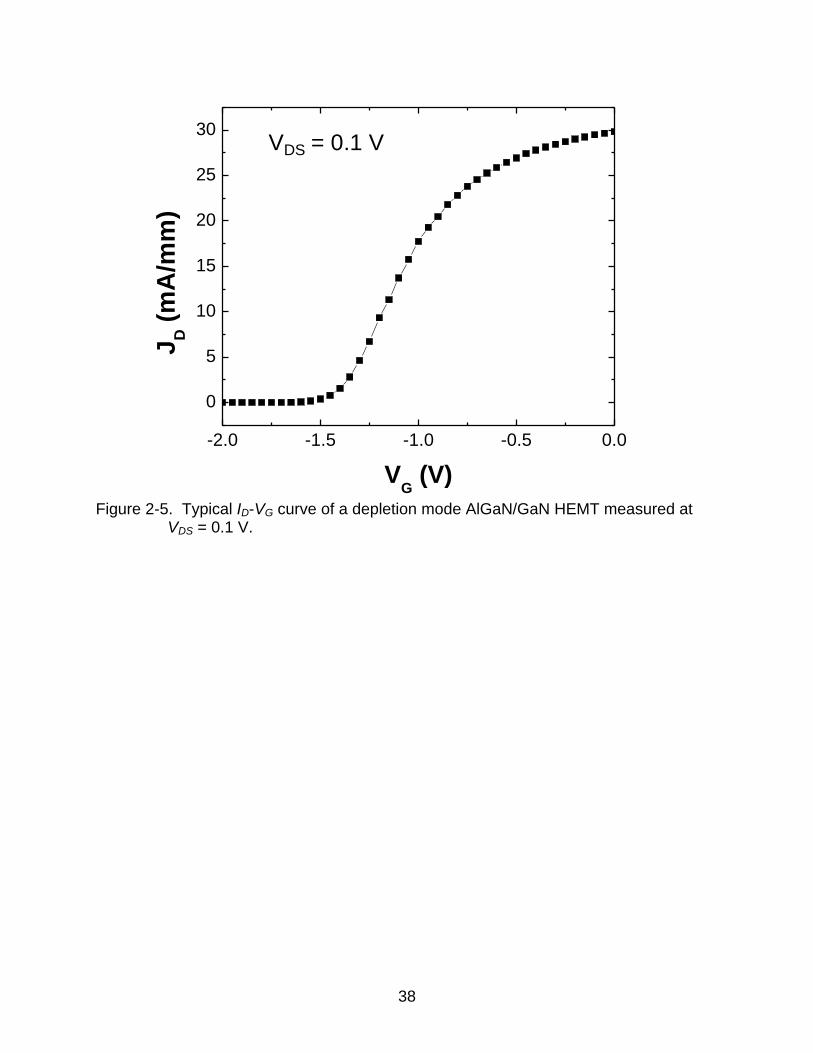
Devices with and without field plates were analyzed. Typical DC ID-VG characteristics
are shown in Figure 2-5 for VDS = 0.1 V. Although these devices were fabricated on a
100 mm diameter wafer, the wafer was diced in approximately 1 cm2 samples to
maximize the number of usable devices for mechanical wafer bending experiments
used to study the effect of stress on the AlGaN/GaN HEMTs.
Mechanical Wafer Bending Experiment Setup
Mechanical wafer bending is a simple and cost effective way to investigate the
underlying physics of strain in semiconductors. Fabricating several wafers with varying
amounts of process-induced stress is expensive, and it can be difficult to accurately
quantify the amount of stress present in to the device. Also, modifying the process flow
to alter the internal stresses can impact other characteristics of the device. Therefore
mechanical wafer bending is fundamental in performing controlled stress experiments.
Several methods have been used to externally apply external mechanical stress to
semiconductors. The first piezoresistance measurements by Smith [14] were achieved
by hanging weights from slabs of semiconductors. This method requires large samples,
therefore only bulk measurements can be taken, and the maximum stress achieved in
Smith’s study is 10 MPa. Bending of cantilevers, or beams anchored at one end is
another possible way to apply stress. While cantilevers are often found in
microelectromechanical systems (MEMS) for transducer and resonator applications, the
stress profile is nonuniform along the length of the beam, making specification of the
31
applied stress difficult. Three-point bending can also be used, however, like cantilevers,
estimation of stress is difficult since stress varies between the three point loads. In this
work, we use a flexure based four-point wafer bending system, capable of applying
greater than 1 GPa of uniaxial stress to Si wafers [47] to isolate the effect of stress on
AlGaN/GaN HEMT devices due to the significantly improved uniformity of stress in the
region between the inner load points.
Four-Point Bending
In four-point bending, a beam is supported by two anchored points while being
deformed by two driving loads as shown in Figure 2-7. Between the center two rods,
the sample is bent with a constant radius of curvature resulting in uniform stress.
Therefore, unlike cantilevers and three-point bending, variation of device position does
not affect the accuracy of the measurements. The magnitude of uniaxial stress on the
top surface of a homogenous material sample between the center two rods can be
represented as [44]
(
) (2-15)
where, E is Young’s modulus, t is the sample thickness, and L and a are rod spacing
distances indicated in Figure 2-6. The magnitude of applied stress was calibrated by
comparing the calculated stress to readings from a noncontact fiber optical
displacement system and strain gauge measurements [45].
Bending Measurements of Small Samples
AlGaN/GaN HEMT samples were diced into ~1 cm2 size to maximize the number
of measureable samples since wafer bending tests are potentially destructive and
AlGaN/GaN HEMT wafers are costly. However, the samples are smaller than the
32
minimum size that can be directly bent in the four-point wafer bending setup. So, to
apply stress to these small samples, we developed a technique to bend small wafer
samples in the standard flexure based wafer bending setup.
This technique of applying mechanical stress to a small AlGaN/GaN HEMT wafer
sample starts by attaching the wafer sample to a heat treated high carbon stainless
steel plate (Figure 2-7). First, the steel strip was sanded with fine grit sand paper to
remove oxidation and to provide a rough surface for adhesion. A thin layer of Epoxy
Technology H74 two part epoxy was then applied to the middle of the steel strip. The
wafer sample was placed on top of the epoxy and pressed down, and excess epoxy
was wiped away. To eliminate air pocket formation during curing of the epoxy, a metal
washer was placed on top of the wafer sample, and the sample was clamped with a
metal binder clip. Then, the sample was inserted into a 100°C oven for 5 minutes. The
washer and metal binder were removed and the sample was placed on a 150°C
hotplate for 5 minutes to complete the curing process. The sample attached to the steel
plate was then inserted into the wafer bending setup.
Under the amount of stress applied (360 MPa) in the experiments, the stainless
steel plate does not permanently deform. A strain gauge is mounted on the top of the
III-V wafer with epoxy to calibrate the stress. As shown in Figure 2-8, stress is applied
and released to the sample. The amount of stress read from the strain gauge returns to
the starting point, verifying that stress applied to the sample is elastic.
To characterize the impact of mechanical stress on the AlGaN/GaN HEMT
devices, electrical measurements need to be taken while simultaneously varying the
amount of applied stress. In order to achieve this, wires were attached to the device
33
bond pads. Standard ball and wedge wire-bonding techniques resulted in delamination
of bond pads destroying the device. Therefore, a novel technique was developed to
attach wires to the bond pads without the use of heat or ultrasonic energy. First, a ball
was formed on the end of a 1 mil Au wire in a ball bonding machine. Then, the wire was
cut to approximately 1 cm length and removed from the ball bonder. A small amount of
electrically conductive Epoxy Technology EE129-4 two part epoxy, was placed on the
end of a probe tip. The probe tip was brought into contact with the end of the wire
without the ball and cured for 24 hours at room temperature. The ball end of the wire
was dipped in conductive epoxy and the probe tip was inserted into the micropositioner.
Using the micropositioner, the ball end of the wire with conductive epoxy was landed on
the device’s bond pad and left to cure for another 24 hours at room temperature. After
the epoxy cured, the micropositioner was lowered to allow slack on the wire for
displacement of the wafer while applying stress.
Summary
The background on the fundamentals of AlGaN/GaN HEMT operation and the
details of the wafer bending experiments were presented. The accumulation of mobile
electrons to form the 2DEG is a result of a net positive charge at the AlGaN/GaN
interface. This interface sheet charge is induced by the difference in polarization
between the AlGaN and GaN layers. The strained AlGaN layer has piezoelectric
polarization as well as spontaneous polarization, whereas the relaxed GaN layer only
has spontaneous polarization. To investigate the impact of mechanical stress on
AlGaN/GaN HEMT devices, four-point mechanical wafer bending is used. Wires are
attached to the device bond pads to simultaneously take electrical measurements while
the level of applied stress is varied.
34
Figure 2-1. GaN-faced GaN crystal lattice, oriented along the <0001> direction.
Ga
N
c
a
z
yx
<0
00
1>
35
Figure 2-2. Polarizations in strained AlxGa1-xN (x = 0.26), relaxed GaN heterostructure.
The strained AlGaN layer has larger spontaneous polarization than the GaN layer, as well as additional polarization from the piezoelectric effect. [Reprinted, with permission, from A.D. Koehler, et al., Extraction of AlGaN/GaN HEMT Gauge Factor in the Presence of Traps, IEEE Elec. Dev. Lett., vol. 31, pp 665-667, Figure 3, May 2010]
0.00
0.02
0.04
0.06
0.08
0.00
0.02
0.04
0.06
PPE,lattice
PSP
PSP
Strained AlGaN
Relaxed GaN
Po
lari
zati
on
(C
/cm
2)
© [2010] IEEE
36
Figure 2-3. Conduction band schematic diagram of an AlGaN/GaN HEMT showing
charge balance.
-30 -25 -20 -15 -10 -5 0 5 10
X (nm)
EC
Ni Gate AlGaN Barrier GaN
sqn
surf
PZ
PZ 2DEG
intQ
37
Figure 2-4. Cross-section SEM of commercial devices characterized in this dissertation.
Image from Nitronex [46].
AlGaN
2DEG GaN
38
Figure 2-5. Typical ID-VG curve of a depletion mode AlGaN/GaN HEMT measured at
VDS = 0.1 V.
-2.0 -1.5 -1.0 -0.5 0.0
0
5
10
15
20
25
30
JD (
mA
/mm
)
VG (V)
VDS = 0.1 V
39
Figure 2-6. Mechanical wafer bending setup: showing (a) a photograph of Si wafer
under ~1 GPa of stress, and (b) a schematic of wafer under four-point bending, showing tensile stress on the top and compressive stress on the bottom with a neutral axis in the middle.
a.
b.
40
Figure 2-7. GaN wafer sample attached to heat treated high carbon stainless steel
inserted in a four-point bending setup.
GaN HEMT wafer
under stressEpoxy
High carbon
steel strip
Probe tip Conductive
epoxy
Gold wire
Steel rods
41
Figure 2-8. Increasing and drecreasing stress applied to a wafer mounted on a
stainless steel strip. A strain gauge is used to determine the amount of applied stress.
0 1 2 3 4 5 6 7 8
0
10
20
30
40
50
60
70
Str
ess
(M
Pa)
Graduation of Stress (#)
42
CHAPTER 3 EXTRACTION OF ALGAN/GAN HEMT GAUGE FACTOR IN THE PRESENCE OF
TRAPS
Introduction
Sensitivity to change in electrical resistance with stress can be represented by a
gauge factor (GF), or the normalized change in resistance (R) per mechanical strain (ε)
(GF = (ΔR/R)/ε). Obtaining an accurate measurement of the gauge factor of
AlGaN/GaN HEMTs is essential in understanding device degradation as well as
improving design of piezoresistive sensors. A large discrepancy in gauge factors (GF)
ranging from -4 to -40,000 for AlGaN/GaN HEMTs are reported in literature (E. Y.
Chang, 2009; Eickhoff, Ambacher, Krotz, & Stutzmann, 2001; Gaska et al., 1998; Kang
et al., 2005, 2004; Yilmazoglu, Mutamba, & Pavlidis, 2006; Zimmermann et al., 2006).
This large disagreement likely results from inaccuracies in resolving the applied stress
and changes in the trapped charge density over the time elapsed during measurement.
These past studies used three-point bending [47-49], cantilevers [50], [52], complex
lever mass system [51], and circular membranes [53] to apply stress, which can be
difficult to accurately quantify the amount of stress applied to the device and therefore
extract the gauge factor. We use four-point bending, while mitigating the effects of
charge traps to experimentally characterize the effect of stress on AlGaN/GaN HEMTs.
Effects of Trapped Charge
The effect of charge trapping due to surface states, traps in the AlGaN barrier, or
bulk traps can lead to measurable changes in device characteristics, such as current
collapse [54], gate-lag [55], drain-lag [55], increased gate leakage [11], threshold © [2010] IEEE. Reprinted with permission from [A.D. Koehler, A. Gupta, M. Chu, S. Parthasarathy, K.J. Linthicum, J.W. Johnson, T. Nishida, S.E. Thompson, Extraction of AlGaN/GaN HEMT Gauge Factor in the Presence of Traps, IEEE Elec. Dev. Lett., vol. 31, pp 665-667, May 2010]
43
voltage shift [56], and light sensitivity [57]. These traps can be formed during
processing and crystal growth [58], or generated during device operation via the inverse
piezoelectric effect [11], or by hot carriers [59]. Trapped electrons between the source
and drain can be modeled as a virtual gate in series with the actual metal gate,
depleting channel electrons. Therefore, the drain current is a function of both the
mechanism supplying electrons to the virtual gate as well as the external bias applied to
the metal gate.
Similar to many AlGaN/GaN HEMTs described in literature, the commercial
devices characterized in this dissertation also exhibit charge trapping effects. The drain
current and threshold voltage depend strongly on the concentration of trapped charge in
the device. Biasing the device during measurements can alter the concentration of
trapped charge, increasing or decreasing the device’s threshold voltage. This instability
in the devices can be demonstrated by first initializing the device with a large VG pulse
(VG = -10 V held for 1 minute), filling available trap states with electrons (right side of
Figure 3-1). Then, 40 consecutive VG sweeps from -2 V to 0 V were performed over
1200 seconds in the dark. These sweeps are unable to maintain the large charge
density of trapped electrons which were filled from the large VG pulse. This results in
electrons thermally detrapping. This in turn, shifts the threshold voltage less negative.
Shining the incandescent microscope light on a device without a field plate photoionizes
trapped charges (left side of Figure 3-1). Consecutive sweeps of VG from -2 V to 1 V in
the dark fills the available traps, shifting the threshold voltage more negative. The
threshold was demonstrated to shift ~0.1 V during 1200 seconds of measurement as
shown in Figure 3-2. Also, it was observed that simply turning on the incandescent
44
microscope light during measurement causes a 15% reduction in channel resistance
(Figure 3-3). In fact, although an enormous gauge factor of -40,000 was reported, the
measured change in resistance was only 15% [53], which could easily result from a
change in trapped charge during the experiment. To eliminate parasitic charge trapping
effects, we developed a technique to expose the sample to continuous sub-bandgap
optical excitation to photoionize trapped charge in order to obtain an accurate gauge
factor measurement.
Experimental Setup
Wafer samples were attached to heat-treated high-carbon steel plates with epoxy
and stressed in a four-point wafer bending setup. Compressive and tensile uniaxial
stress up to 360 MPa was applied longitudinal to the channel direction. To obtain an
accurate measurement of the AlGaN/GaN HEMT gauge factor, parasitic charge
trapping transients and external resistances were addressed. After the effects of
charge trapping were eliminated, and external resistances were accounted for, an
accurate gauge factor measurement was performed.
Elimination of Charge Trapping Effects
To combat the instability issue associated with trapped charges, the HEMT device
was exposed to light with a photon energy near, but below the band-gap of GaN (~3.4
eV or 365 nm wavelength) to photoionize all trapped electrons influencing the
resistance measurement without band-to-band generation of electron-hole pairs.
Initially, a mercury arc ultraviolet (UV) spotlight with peak wavelength of 377.7 nm or
3.284 eV was chosen to illuminate the device under test. A sweep of ID-VG under UV
spotlight illumination compared to dark (Figure 3-4a) showed a large increase in off-
state drain current and a decrease in subthreshold slope. The spectral intensity of the
45
light source was measured in a spectrometer. A significant portion of the photon energy
was above the band-gap of GaN (3.39ev ~ 365 nm) as shown in Figure 3-4b. Under
illumination of above bandgap light, mobile electron-hole pairs are photogenerated. An
increase in off-state current and a decrease in subthreshold slope are consistent with
carrier photogeneration. A 380 nm band-pass filter was measured to filter out
wavelengths below 365 nm (Figure 3-5b). A horizontal shift in subthreshold slope and
similar off-state leakage current (Figure 3-5a) verifies a decrease in the effect of trapped
charge without photogeneration of electron-hole pairs.
A schematic of the experimental setup is shown in Figure 3-6. The standard wafer
bending setup described in Chapter 2 is illuminated by the UV light source. The band-
pass filter is mounted in a 4 inch thick polystyrene heat shield to block ambient heat
from the mercury arc lamp and block nonfiltered light from illuminating the device. As
shown in Figure 3-7, over 1500 seconds, the change of the measured channel
resistance is less than 0.02%. Since the resistance measurement has been stabilized,
it is now appropriate to apply stress to monitor the gauge factor.
External Resistance Consideration
The stress dependence of the channel resistance (RCH) was measured at VGS = -
1V and VDS = 0.1V, by excluding source/drain contact resistances. The high
conductivity of GaN 2DEG results in a small channel resistance, especially for the
commercial devices characterized with W/L ratio of 25. The measured resistance
(Rmeas) is the sum of the channel resistance (RCH), source contact resistance (RS), drain
contact resistance (RD), and external parasitic resistances (Rext) and was on the order of
100 Ω.
46
(3-1)
The source and drain contact resistances (RS = RD = 5 Ω), measured by transmission
line measurements, are subtracted from the measured resistance and are assumed to
have a negligible stress dependence. A four-point Kelvin measurement is used to
eliminate the effect of external resistances. Two wires were bonded to both the source
and drain pad and one to the gate. One pair of source and drain contacts are used to
supply a dc current via the force connections on the semiconductor parameter analyzer.
The other pair of connections are used to sense the voltage drop across the source and
drain pads.
Results and Discussion
Gauge Factor Measurement
Longitudinal uniaxial stress was varied in 60 MPa increments and held for 100
seconds at each interval. The normalized change in RCH was measured for
incrementally applied compressive and tensile stress up to 360 MPa, which was then
released incrementally to zero as shown by the dotted lines of Figure 3-8. Tensile
stress decreases RCH, while compressive stress increases RCH are seen by the solid
experimental lines of Figure 3-8. At the maximum applied stress (360 MPa), the
normalized resistance change was ~0.83%/100 MPa, which is much smaller than what
is observed in (001)/<110> silicon nMOSFETs of 3.2%/100 MPa [60]. The resistance
returned to the initial unstressed value after increasing and decreasing the compressive
and tensile stress. This demonstrates that the change in resistance observed is due to
a reversible strain effect, opposed to charge trapping/detrapping transients.
The gauge factor was determined by averaging the RCH measurements over each
time interval during which the stress was held constant (Figure 3-9). Error bars

47
represent a three standard deviation confidence interval for the measurement. The
slope of a total least squares linear fit of the averaged RCH versus strain curve was
obtained to determine a gauge factor of -2.5 ±0.4. Total least squares analysis included
uncertainty of the measurements. The determined gauge factor (-2.5 ±0.4) is small
relative to values in literature ranging from -4 to -40,000 [47-53].
Resistance Change with Stress
To provide understanding of the small measured gauge factor, the factors
influencing the change in channel resistance with stress are investigated. The channel
resistance is inversely related to the 2DEG sheet carrier density and electron mobility
(μe).
(3-2)
where the A is cross sectional area of the 2DEG. In the presence of stress, the
normalized change in channel resistance can be written as:
(3-3)
To evaluate the effect of stress on the channel resistance, both the effect of stress on
the 2DEG sheet carrier density and mobility needs to be considered.
2DEG Change with Stress
To analyze the effect of stress on the 2DEG sheet carrier density, the additional
piezoelectric polarization induced by mechanical wafer bending must be analyzed.
Mechanical wafer bending induces additional polarization in the <0001> direction.
Stress resulting from uniaxial mechanical wafer bending is approximately equal in both
the AlGaN barrier and the GaN layer because the AlGaN barrier (18 nm) and GaN layer
48
(1 μm) are thin compared to the total thickness of the wafer (150 μm). Therefore, these
two layers are near the top surface of the sample, far from the neutral axis of bending,
and experience the same magnitude of stress. Spontaneous polarization in both the
AlGaN and GaN remains unchanged by wafer bending since it is an intrinsic material
parameter. As shown in Figure 3-10 for 1 GPa of uniaxial tensile stress, mechanical
wafer bending induced piezoelectric polarization (PPE,mech.) adds to the polarization in
both the AlGaN and GaN layers [57]. The magnitude of the mechanical wafer bending
induced piezoelectric polarization is calculated for uniaxial stress where
σxx is the only nonzero element in the stress tensor, and . The mechanical
wafer bending induced piezoelectric polarization is similar for both AlGaN (0.00148
C/cm2) and GaN (0.00143 C/cm2) since the elastic and piezoelectric coefficients in GaN
and AlGaN are similar for a small Al mole fraction (26%). The total polarization at the
interface under uniaxial mechanical stress is
(
) (
) (3-4)
Relating the total polarization at the interface to ns according to Ambacher et al. [61]
gives an increase in ns ranging from 0.064% to 1% for 360 MPa of tensile stress.
Uncertainty of ns results from variation in stiffness constants and piezoelectric
coefficients reported in literature [62-70].
Electron Mobility Change with Stress
Strain-enhanced mobility can result from reduced average conductivity effective
mass from carrier repopulation and band warping, suppression of intervalley scattering
from subband splitting, and change in density of states with stress. Unlike Si, GaN is a
direct semiconductor with a non-degenerate conduction band minimum at the Γ-point.

49
Therefore, stress-induced change of the average effective mass due to electron
repopulation and scattering can be neglected. Thus, the mobility change is dominated
by a change in the effective mass through band warping. Band warping can be
simulated using a tight-binding model with a sp3d5 basis [71]. Since strain alters the
atomic positions, and consequently the bond lengths and bond angles strain modifies
the elements of the new Hamiltonian matrix. Solving for the eigenvalues of the strained
matrix allows the strain effect on the effective mass to be calculated. Mobility
enhancement from a reduction in effective mass was determined to be 0.29% to 0.49%
for 360 MPa of stress [72].
Simulated Gauge Factor
Figure 3-10 shows the experimental normalized change in RCH with stress (symbols)
compared to the calculation (shaded bands). The change in 2DEG sheet carrier density
and mobility is combined using Equation 3-3 to calculate the normalized change in
resistance. Depending on the coefficient values used in the calculation, the change in
RCH can range from 0.29% to 1.5% for 360 MPa of stress illustrated as shaded bands in
Figure 3-11. This corresponds to a GF of -7.9 ±5.2. Comparing the experimental
results with the model, the best fitting set of elastic and piezoelectric coefficients from
literature is Cij(GaN) [73] Cij(AlN) [74] eij(GaN) [75] eij(AlN) [76].
Summary
Illuminating the AlGaN/GaN HEMT device with photon energy near but below the
band-gap of GaN provided a reliable gauge factor measurement. After eliminating trap
charging effects, the gauge factor of the AlGaN/GaN HEMT was determined to be -2.8
±0.4. A reliable gauge factor measurementThe small gauge factor indicates a small
stress dependence on the device resistivity. This is explained by small changes in the
50
2DEG sheet carrier density and channel mobility. The experimental results were
compared with simulated gauge factor (-7.9 ±5.2) to determine the best fitting set of
elastic and piezoelectric coefficients of GaN and AlN.
51
Figure 3-1. Results of consecutive VGS = -2 to 0 VDS = 0.1 V measurement sweeps
resulting in charge trapping and detrapping.
Gate AlGaN GaN
40 Consecutive VGS = -2 to 0 VDS = 0.1 V measurements (1200 s)
detrapping
trapping
Large VG pulse (VG = -10 V for 1 minute)
Gate AlGaN GaN
VG (V)
ID (m
A)
0-2 -1 -0.5-1.5
2
0
1
1.5
0.5
Dark Light
52
Figure 3-2. VT measured in consecutive ID – VG sweeps. In dark, |VT| can increase
(decrease) from detrapping (trapping) of electrons, depending the device initialization. Under unfiltered UV illumination, VT does not fluctuate.
-1.6
-1.5
-1.4
-1.3
-1.2
0 200 400 600 800 1000 1200
VT
(V)
Time (s)
initialized by UV light (1 min)
(measured in dark)
measured under UV light
initialized by VGS = -10 V for 1 minute
(measured in dark)
Detrapping
Trapping
Stable
0 200 400 600 800 1000 1200
-1.2
-1.3
-1.4
-1.5
-1.6
Time (s)
VT
(V)
53
Figure 3-3. A decrease in channel resistance of 15% observed during 1200 seconds of
measuring after turning on the incandescent microscope light.
0 200 400 600 800 1000
-15
-10
-5
0
R
TO
T/R
TO
T (
%)
Time (s)
15% change in RTOT
from detrapping
Microscope Light ON
VDS = 0.1 V
VGS = -1 VΔ
RC
H/R
CH
(%)
Time (s)
15%
54
Figure 3-4. Unfiltered UV measurement (a) ID-VG measurements in dark and under
unfiltered UV light with a large increase in off-state current and a decrease in subthreshold slope. (b) The spectral output of the unfiltered UV light.
3.0 3.2 3.4 3.6 3.80
5
10
Inte
nsit
y (
au
)
Energy (eV)
420 400 380 360 340 320
Wavelength (nm)
EG(GaN)
≈
-2.0 -1.8 -1.6 -1.4 -1.2 -1.0
10-7
10-6
10-5
10-4
10-3
I D
(A
)
VG (V)
Under UV
DarkLarge
Increase
a. b.
55
Figure 3-5. Filtered UV measurement (a) ID-VG measurements in dark and UV light
filtered by a 380 nm bandpass filter with a much smaller increase in off-state current and no subthreshold slope change. (b) The spectral output of UV light with 380 nm bandpass filter.
3.0 3.2 3.4 3.6 3.8
0.0
0.1
0.2
0.3
0.4
Inte
ns
ity
(a
u)
Energy (eV)
420 400 380 360 340 320
Wavelength (nm)
EG(GaN)
≈
-1.6
10-7
10-6
10-5
10-4
10-3
I D (
A)
VG (V)
Under UV
Dark
Much Smaller
Increase
Under UV
with filter
a. b.
56
Figure 3-6. Experimental setup for photoionizing trapped charge to measure the gauge
factor.
Polystyrene heat shield
Band-pass filter
UV source
GaN HEMT waferunder stress
EpoxyHigh carbonsteel strip
Probe tip Conductiveepoxy
Gold wire
Steel rods
57
Figure 3-7. Illuminating the device under test with UV light stabilized RCH to less than
0.02% variation for 1200 seconds of measurement.
0 500 1000 1500 2000
1.38
1.39
1.40
1.41
1.42
1.43
RT
OT (
)
Time (s)
ON
Filte
red
UV
Lig
ht
VGS = -1 V, VDS = 0.1 V
ΔRTOT < 0.02%
OFF
Sample A
ΔR
CH
(Ω)
ΔRCH < 0.02%
58
Figure 3-8. Normalized change in channel resistance with incrementally increasing and
decreasing uniaxial stress. [Reprinted, with permission, from A.D. Koehler, et al., Extraction of AlGaN/GaN HEMT Gauge Factor in the Presence of Traps, IEEE Elec. Dev. Lett., vol. 31, pp 665-667, Figure 2, May 2010]
Compression
Tension
0 500 1000 1500
-0.3
-0.2
-0.1
0.0
0.1
0.2
0.3
RT
OT / R
TO
T (
%)
Time (s)
600
400
200
0
-200
-400
-600
Stre
ss
Ma
gn
itud
e (M
Pa)
ΔR
CH/R
CH
(%)
© [2010] IEEE
59
Figure 3-9. RCH measurements at each time interval stress was held constant. Error
bars represent a three standard deviation confidence interval for the measurement. [Reprinted, with permission, from A.D. Koehler, et al., Extraction of AlGaN/GaN HEMT Gauge Factor in the Presence of Traps, IEEE Elec. Dev. Lett., vol. 31, pp 665-667, Figure 4, May 2010]
-400 -300 -200 -100 0 100 200 300 400
-0.4
-0.2
0.0
0.2
0.4
RC
H/R
CH (
%)
Stress (MPa) © [2010] IEEE
60
Figure 3-10. Schematic showing polarizations in AlGaN/GaN HEMTs as fabricated
(left), and 1 GPa mechanically applied stress (right) generating additional PPE,mech similar in magnitude for both AlGaN and GaN layers. [Reprinted, with permission, from A.D. Koehler, et al., Extraction of AlGaN/GaN HEMT Gauge Factor in the Presence of Traps, IEEE Elec. Dev. Lett., vol. 31, pp 665-667, Figure 3, May 2010]
0.00
0.02
0.04
0.06
0.08
0.00
0.02
0.04
0.06
PPE,lattice
PSP
PSP
AlGaN
GaN
Po
lari
za
tio
n (
C/c
m2)
0.00
0.02
0.04
0.06
0.08
Po
lari
za
tio
n (
C/c
m2)
0.00
0.02
0.04
0.06
PPE,lattice
PSP
PSP
AlGaN
GaN
PPE,mech.
PPE,mech.
As-Fabricated Mechanical Bending
© [2010] IEEE
61
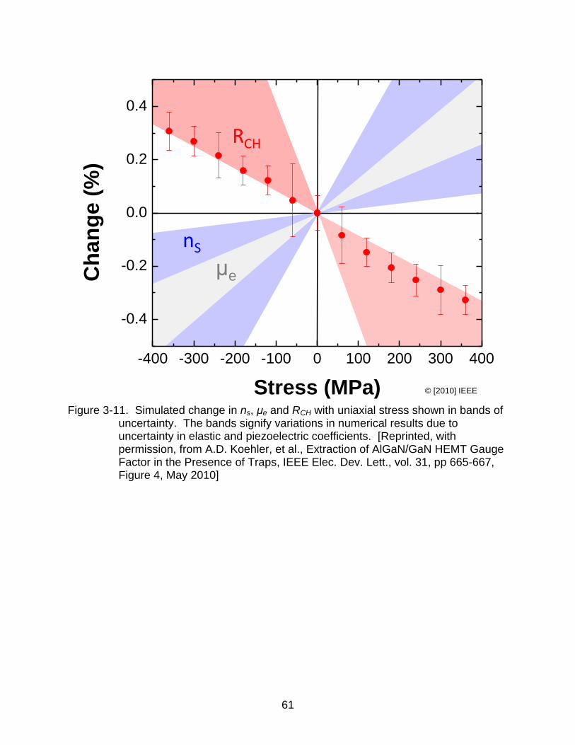
Figure 3-11. Simulated change in ns, μe and RCH with uniaxial stress shown in bands of
uncertainty. The bands signify variations in numerical results due to uncertainty in elastic and piezoelectric coefficients. [Reprinted, with permission, from A.D. Koehler, et al., Extraction of AlGaN/GaN HEMT Gauge Factor in the Presence of Traps, IEEE Elec. Dev. Lett., vol. 31, pp 665-667, Figure 4, May 2010]
μe
nS
RCH
-400 -300 -200 -100 0 100 200 300 400
-0.4
-0.2
0.0
0.2
0.4
Ch
an
ge
(%
)
Stress (MPa) © [2010] IEEE
62
CHAPTER 4 VERTICAL ELECTRIC FIELD IN THE ALGAN BARRIER
Introduction
Reliability is a major concern with AlGaN/GaN HEMTs, and a systematic study of
the impact of stress on gate leakage current is essential to gain physical insight into the
degradation mechanisms in order to improve device reliability. Gate leakage currents
for AlGaN and GaN Schottky interfaces in literature are significantly larger than what
would be theoretically predicted based purely on the thermionic emission model [77].
Determining the dominant gate leakage transport mechanism through the AlGaN barrier
in AlGaN/GaN HEMT is necessary for investigating the physics behind the effect of
stress on the gate leakage current. An accurate determination of the electric field in the
AlGaN barrier (EAlGaN) is required to investigate the gate leakage models.
Several models have been proposed to explain the gate leakage mechanism in
AlGaN/GaN HEMTs, such as trap-assisted tunneling [34], [78-81], direct or Fowler-
Nordheim (FN) tunneling [78-80], [82], temperature assisted tunneling [78], [83], multi-
step trap-assisted tunneling [84], thermionic trap assisted tunneling [82], [85-87],
tunneling through a thin surface barrier [88], and Poole-Frenkel (PF) emission [89-94].
The dominant leakage mechanism is strongly dependent on the materials and
processing conditions and the electric field in the AlGaN Barrier, EAlGaN. To characterize
the effect of mechanical stress on the state-of-the-art commercial AlGaN/GaN devices,
an accurate model for the leakage mechanism is necessary. To compare different
leakage models to the experimental measurements, an accurate calculation of EAlGaN is
needed. In past works, EAlGaN has been simplified to a linear relationship with the gate
voltage [91][89], simulated using Medici 2D simulations [95], and experimentally
63
measured [96]. The VDS = 0 state is of particular interest for exploring reliability since
both the source and drain sides of the device gate are electrically stressed
simultaneously. A complete investigation of the electric field relationship as a function
of VG at the VDS = 0 state will be presented.
Ideal 1D Calculation of EAlGaN
A one-dimensional (1D) calculation of EAlGaN provides insight into the general
relationship between voltage and field. In this condition, the gate is assumed to be
infinitely wide. Also, for simplicity, EAlGaN is assumed to be a constant throughout the
entire thickness of the AlGaN barrier. Based on these assumptions, a simple
expression for the electric field in the AlGaN barrier can be derived from the voltage
drop across the AlGaN barrier (VAlGaN) from inspection of the energy band diagram
(Figure 4-1). EAlGaN can be written as,
( )
(4-1)
Recalling Equation 2-11, ns can be rewritten in terms of EAlGaN,
(
)
(4-2)
Then, the simple expression for EAlGaN is
(4-3)
In the expression for EAlGaN (Equation 4-3), only the 2DEG sheet carrier density
(ns) is a function of gate voltage. The total fixed charge density at the AlGaN/GaN
interface (σint) is assumed to be independent of bias because it is based on the
polarization. Charge trapped at the AlGaN/GaN interface is estimated to be constant
64
with bias. To analyze the dependence of ns with gate voltage, ns is rewritten to include
the contribution of VG in terms of the equilibrium 2DEG concentration ns0.
(
) (
) (4-4)
where,
is the AlGaN capacitance per unit area. At equilibrium, VG = 0 V
and ns = ns0, which is the maximum induced 2DEG sheet carrier density. The fixed
positive charge at the AlGaN/GaN interface induces accumulation of electrons at the
interface in the GaN. The electrons that form the 2DEG originate from the AlGaN
surface [42], not from the source, drain, and substrate as in a Si MOSFET inversion
layer. A negative bias applied to the gate depletes the 2DEG, decreasing ns linearly, as
shown by Equation 4-4. The threshold voltage for the depletion mode AlGaN/GaN
HEMT is defined as the voltage required on the gate to entirely deplete the 2DEG (ns =
0). Since the AlGaN/GaN HEMT is a depletion mode device with a negative VT, the
device is considered to be turned off below threshold (|VG| > |VT|). Above threshold, the
2DEG is formed (|VG| < |VT|). Below threshold, the 2DEG remains depleted. Since the
intrinsic carrier concentration of GaN is extremely low (ni ~ 1 x 10⁻¹⁰ cm-3 at 300 K), hole
accumulation at the surface is negligible. Figure 4-2 shows for an ideal device, without
interface trapped charge, the 2DEG sheet carrier density plotted against VG. The
charge at the AlGaN/GaN interface (σint = 2.2 x 10⁻⁶ C/cm2) is only a result of the
polarization differences between AlGaN and GaN. Parameters described in Table 4-1
were used for the calculation.
To express EAlGaN as a function of gate voltage, the voltage dependent 2DEG
equation (Equation 4-4) was incorporated into the expression for EAlGaN (Equation 4-3)
to give,
65
( ) (
)
(4-5)
For gate bias below threshold, EAlGaN saturates at ( ). Figure 4-3
shows EAlGaN increasing linearly with bias for gate biases above threshold.
1D Experimentally Measured EAlGaN
Estimation of EAlGaN for an actual AlGaN/GaN HEMT device based on the 1D
model requires both σint and ns to be experimentally measured. The threshold voltage
determined by the standard linear extrapolation method (VT = -1.4 V) is not consistent
with the definition of VG = VT when ns = 0. A more appropriate threshold of -1.9 V is
used based on the initial increase of the capacitance-voltage curve (Figure 4-5).
Trapped charge in the actual device reduces the amount of fixed charge at the
AlGaN/GaN interface, shifting the threshold voltage more positive than the ideal value.
From Equation 4-4 and the definition of threshold (VG = VT when ns = 0), the 2DEG
sheet carrier density at VG = 0 can be calculated from the measured VT.
(4-6)
Which gives ns0 = 5.3 x 1012 cm-3 for VT = -1.9 V. Then, the fixed charge at the
AlGaN/GaN interface can be estimated by solving for σint in Equation 2-12.
(
) (4-7)
Resulting in σint = 1.25 x 10⁻⁶ C/cm2, which is nearly half the ideal value (σint = 2.2
10-6 C/cm2) using the constants in Table 4-1. The interface trapped charge density is
estimated from the subthreshold slope (SS) measurements [97], [98]
66
[
] (4-8)
The capacitance associated with the interface trapped charge (Cit) can be related
to the density of interface traps by Cit = qDit. For the measured device with SS = 100
mV/dec, the interface trap density is Dit = 1.92 x 1012 cm-2eV-1. Assuming all traps are
full, integrating over the bandgap of AlGaN gives an interface trapped charge Qit = 1.2 x
10-6 C/cm2. Figure 4-4 shows a bar chart of the charge density in the ideal device
compared to the actual device. In the ideal device (Qit = 0) σpz = σint. However, in the
actual device, fixed charge at the AlGaN/GaN interface induced by polarization is
reduced by negative trapped charge.
To obtain EAlGaN for the actual device, the ns versus VG relationship needs to be
obtained. A high-frequency (1 MHz) capacitance-voltage curve (Figure 4-5) was
integrated from pinch-off to voltage V. The experimental bias range was limited to VG =
-2 V to 0 V to avoid additional charge trapping from larger applied biases. The value of
ns(V) is also shown in Figure 4-5. The experimentally obtained ns versus VG
relationship is used in Equation 4-3 to calculate the experimentally obtained EAlGaN
versus VG relationship.
Implementing the experimentally determined σint and ns versus VG relationship
provides the experimentally determined 1D calculation of EAlGaN versus VG. Figure 4-6
shows a comparison between the experimental and ideal 1D calculation for EAlGaN
versus VG. Since both methods are based on the 1D expression, they have similar
trends. Above threshold, |EAlGaN| increases linearly with increasing reverse bias, and
below threshold EAlGaN saturates at ( ). The presence of Qit reduces
σint and the magnitude of the saturated value of EAlGaN below threshold in the actual
67
device compared to the ideal 1D calculation. In addition, VT is shifted toward the
positive direction by the negative Qit. At VG = 0, the experimental |EAlGaN| is larger than
the ideal 1D case because the experimentally extracted ns0 is lower than what is
theoretically predicted, making the numerator of Equation 4-3 larger.
2D Simulation of EAlGaN
Simulation Details
The AlGaN/GaN HEMT structure was simulated using the Sentaurus device
simulator. A two-dimensional (2D) simulation was performed to gain a physical
understanding of 2D effects on EAlGaN. The thin (~1.5 nm) GaN cap layer was neglected
in the simulation for simplicity. The device structure is quantized into a mesh or grid of
discrete elements. The grid was condensed in areas where large variations of carrier
concentration are expected at short distances to optimize computational accuracy
(Figure 4-7).
At each point on the grid, three variables are solved for simultaneously. The
electrostatic potential, electron concentration, and hole concentration are solved for
through Poisson’s equation and the electron and hole continuity equations respectively.
The boundary conditions used to solve for the three variables are: the metal-contact
work function difference, the ohmic contacts at the source and drain, and local
conservation of charge. In the actual device, the high resistivity Si layer isolates the
GaN layer from the back side of the wafer, leaving it electrically floating. The bulk is left
floating in simulation to model this. Shockley-Read-Hall recombination and generation
were included in the calculation. Also, a hydrodynamic model was used where the
carrier temperature is not assumed to be equal to the lattice temperature. Electron
mobility was modeled including doping dependence, high field saturation, and
68
temperature. Doping was introduced under the source and drain contacts to emulate
metal spikes to provide an ohmic contact to the 2DEG [99]. The piezoelectric effect is
modeled by incorporating a fixed charge at the AlGaN/GaN interface equal to σint and at
the AlGaN surface equal to σPZ to match experiment. The parameters used in the
simulation are given in Table 4-1.
Simulation Results
The simulated dependence of EAlGaN versus VG at the center of the gate is
compared to the 1D model with experimentally determined parameters (Figure 4-8). In
the simulation, σint was matched to the experimentally obtained value of 1.25 x 10⁻⁶
C/cm2. The trend of the 2D simulated EAlGaN is similar to the 1D calculation. Above
threshold, |EAlGaN| increases until threshold with decreasing reverse gate bias. Below
threshold, |EAlGaN| tends to saturate. Although σint is matched, the saturation value of
EAlGaN in the 2D simulation at the center of the gate is slightly lower than the
experimentally determined curve. Since the simulated device has a finite gate width (1
μm), it is important to analyze the edges of the gate for a comprehensive understanding
of the EAlGaN versus VG relationship.
Vertical cross-section plots of EAlGaN through the middle of the gate and drain edge
of the gate are shown in Figure 4-9. The AlGaN/GaN interface is referenced at y = 0
μm and the AlGaN surface is at y = -0.018 μm. In the middle of the gate, EAlGaN remains
essentially constant throughout the depth of the AlGaN layer for VG = -2 to -10 V. As
shown in Figure 4-5, the magnitude of EAlGaN increases more above VT than below VT as
a function of VG, demonstrating the saturation of EAlGaN below VT. However, at the gate
edge, EAlGaN varies with depth in the AlGaN barrier, and EAlGaN continues increasing with
increasing reverse gate bias.
69
A horizontal cross section 1 nm below the gate contact in the AlGaN barrier shows
a large increase in EAlGaN at the gate edges (Figure 4-10). At VG = 0 V, |EAlGaN| is lower
directly under the Schottky gate than under the passivation layer. This is a result of the
negative polarization charge at the top surface of the AlGaN. Under the nitride, the
surface polarization exists, however, the gate has control of the potential under the gate
electrode.
To explain the large increase in EAlGaN at the gate edges, a plot of the potential at
the GaN surface, 0.5 nm below the AlGaN/GaN interface is shown (Figure 4-11). At
large reverse gate biases, there is a large horizontal potential drop in the GaN surface
near the gate edges. This potential drop results in a large horizontal electric field at the
gate edge. The horizontal field at the gate edge is much larger than in the center of the
gate (Figure 4-12). The contribution of the horizontal electric field at the gate edge adds
to the vertical electric field increasing the magnitude of EAlGaN increasing at the gate
edges.
Summary
The relationship between EAlGaN and VG was calculated for an ideal 1D device. It
was experimentally matched to the actual device, and a 2D simulation was performed.
A 1D model was used to investigate the dependence of EAlGaN with VG. Adjusting σint
and ns based on experimental measurements provides an accurate relationship above
threshold. The 1D model fails to capture the edge physics of a realistic device. 2D
Sentaurus device simulation showed the 1D model is accurate above threshold, but
below threshold, EAlGaN at the gate edges continues increasing. Above threshold,
|EAlGaN| increases linearly with increasing reverse gate bias and the field is
approximately constant throughout the depth of the AlGaN layer. Below threshold, VG <

70
VT, 2D effects change the field profile. In the middle of the gate, EAlGaN saturates, but at
the gate edges, EAlGaN increases. With the relationship between EAlGaN and VG
understood, this relationship can be used to explain the gate leakage transport
mechanism in the AlGaN/GaN HEMT.
71
Table 4-1. List of parameters used in 1D EAlGaN calculation
Parameter Symbol Value Units
Temperature T 300 K Intrinsic carrier concentration ni 10-10 cm-3
AlGaN thickness tAlGaN 18 nm Permittivity of GaN 9.5 - Permittivity of AlN 8.5 -
Bandgap of GaN EG,GaN 3.4 eV Bandgap of AlN EG,AlN 6.13 eV
Electron affinity of GaN 4.1 eV Ni work function 5.27 eV
Mass of GaN m*GaN 0.2*m0 - Mass of AlN m*AlN 0.48*m0 -
Fixed charge at AlGaN/GaN interface σint 2.2 x 10⁻⁶ C/cm2
72
Figure 4-1. Energy band diagram schematic showing Ni/AlGaN/GaN interface
VG = 0
b
CE
CE
0FE FE
AlGaNV
AlGaNE
Ni AlGaN GaN
AlGaNt
73
Figure 4-2. Dependence of the 2DEG density (ns) with gate bias for the 1D case, with
no interface trapped charge. Threshold is defined when ns is entirely depleted (ns = 0).
-10 -8 -6 -4 -2 00
2
4
6
8
10
12x 10
12
Ele
ctro
n D
en
sity
(cm
-2)
VG (V)
VT
ns0
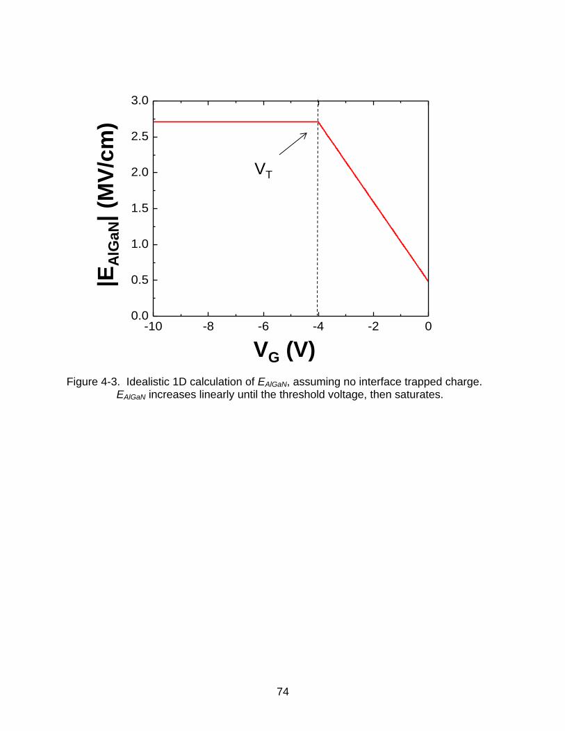
74
Figure 4-3. Idealistic 1D calculation of EAlGaN, assuming no interface trapped charge.
EAlGaN increases linearly until the threshold voltage, then saturates.
-10 -8 -6 -4 -2 00.0
0.5
1.0
1.5
2.0
2.5
3.0
VT
|EA
lGaN|
(MV
/cm
)
VG (V)
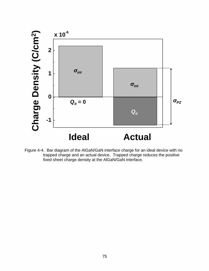
75
Figure 4-4. Bar diagram of the AlGaN/GaN interface charge for an ideal device with no
trapped charge and an actual device. Trapped charge reduces the positive fixed sheet charge density at the AlGaN/GaN interface.
-1
0
1
2
x 10-6
Ch
arg
e D
en
sit
y (
C/c
m2)
Ideal Actual
Qit = 0
Qit
σint
σint
σPZ
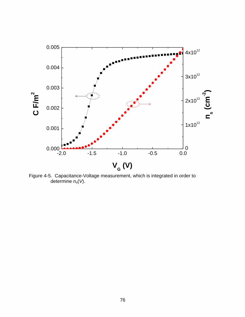
76
Figure 4-5. Capacitance-Voltage measurement, which is integrated in order to
determine ns(V).
-2.0 -1.5 -1.0 -0.5 0.00.000
0.001
0.002
0.003
0.004
0.005
C
F/m
2
VG (V)
0
1x10¹²
2x10¹²
3x10¹²
4x10¹²
ns (
cm
-2)
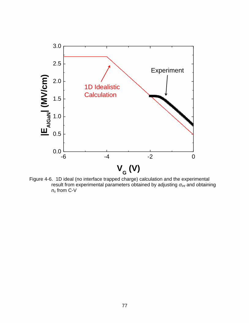
77
Figure 4-6. 1D ideal (no interface trapped charge) calculation and the experimental
result from experimental parameters obtained by adjusting σint and obtaining ns from C-V
-6 -4 -2 00.0
0.5
1.0
1.5
2.0
2.5
3.0
|EA
lGaN|
(MV
/cm
)
VG (V)
Experiment
1D Idealistic
Calculation
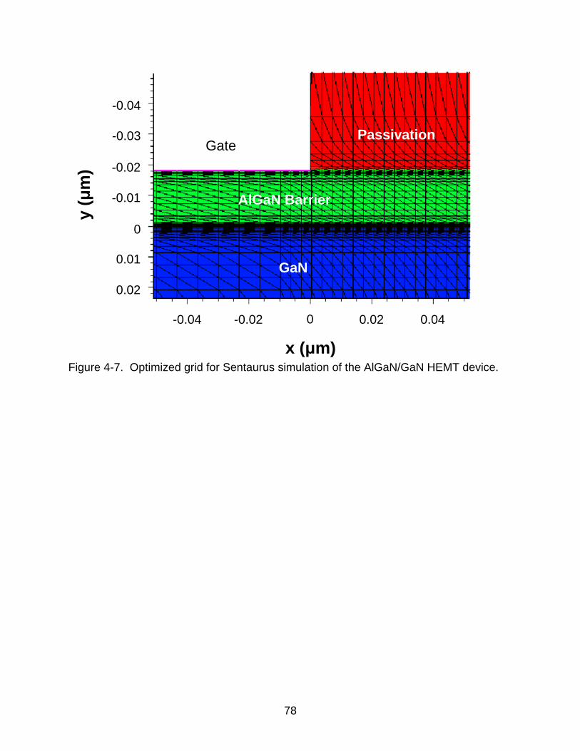
78
Figure 4-7. Optimized grid for Sentaurus simulation of the AlGaN/GaN HEMT device.
Passivation
AlGaN Barrier
GaN
Gate
0.02
-0.03
0
-0.02
-0.04
0.02
0.01
y (μ
m)
x (μm)
0.04-0.04 -0.02 0
-0.01
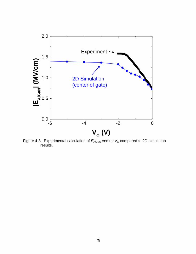
79
Figure 4-8. Experimental calculation of EAlGaN versus VG compared to 2D simulation
results.
-6 -4 -2 00.0
0.5
1.0
1.5
2.0|E
AlG
aN|
(MV
/cm
)
VG (V)
Experiment
2D Simulation
(center of gate)
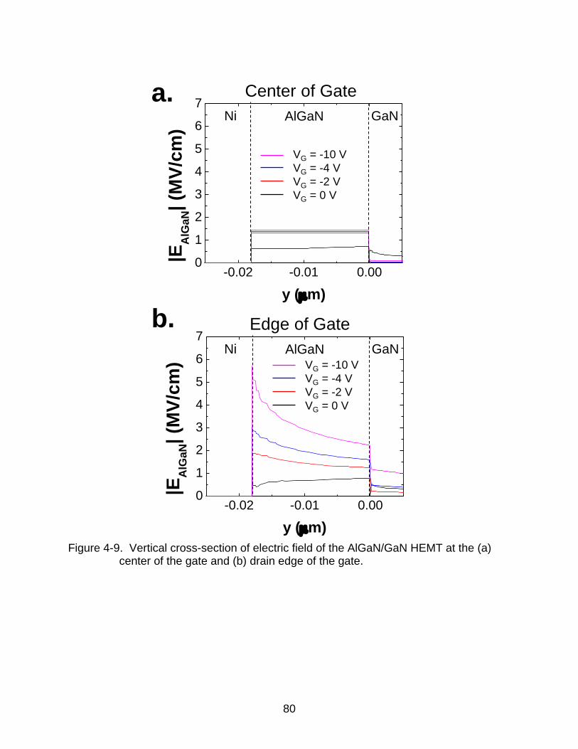
80
Figure 4-9. Vertical cross-section of electric field of the AlGaN/GaN HEMT at the (a)
center of the gate and (b) drain edge of the gate.
-0.02 -0.01 0.000
1
2
3
4
5
6
7
|EA
lGaN|
(MV
/cm
)
y (m)
-0.02 -0.01 0.000
1
2
3
4
5
6
7
|EA
lGaN|
(MV
/cm
)
y (m)
Center of Gate
Edge of Gate
VG = -10 V
VG = -4 V
VG = -2 V
VG = 0 V
VG = -10 V
VG = -4 V
VG = -2 V
VG = 0 V
Ni AlGaN GaN
Ni AlGaN GaN
a.
b.
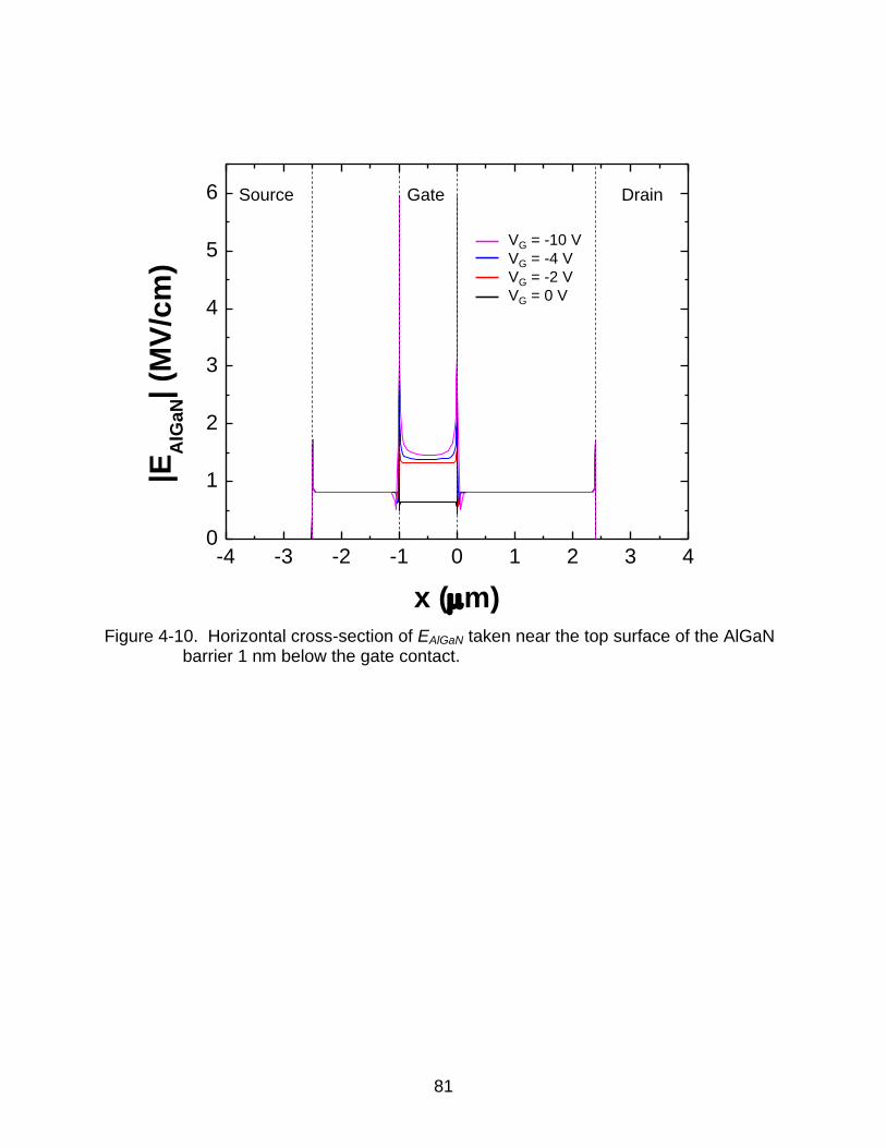
81
Figure 4-10. Horizontal cross-section of EAlGaN taken near the top surface of the AlGaN
barrier 1 nm below the gate contact.
-4 -3 -2 -1 0 1 2 3 40
1
2
3
4
5
6
|EA
lGaN|
(MV
/cm
)
x (m)
VG = -10 V
VG = -4 V
VG = -2 V
VG = 0 V
Source Gate Drain
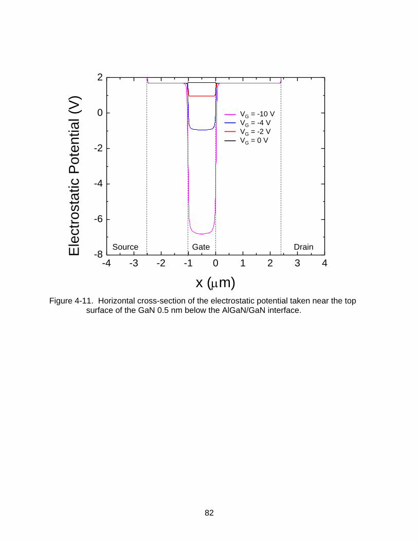
82
Figure 4-11. Horizontal cross-section of the electrostatic potential taken near the top
surface of the GaN 0.5 nm below the AlGaN/GaN interface.
-4 -3 -2 -1 0 1 2 3 4-8
-6
-4
-2
0
2E
lectr
osta
tic P
ote
ntial (V
)
x (m)
VG = -10 V
VG = -4 V
VG = -2 V
VG = 0 V
Source Gate Drain
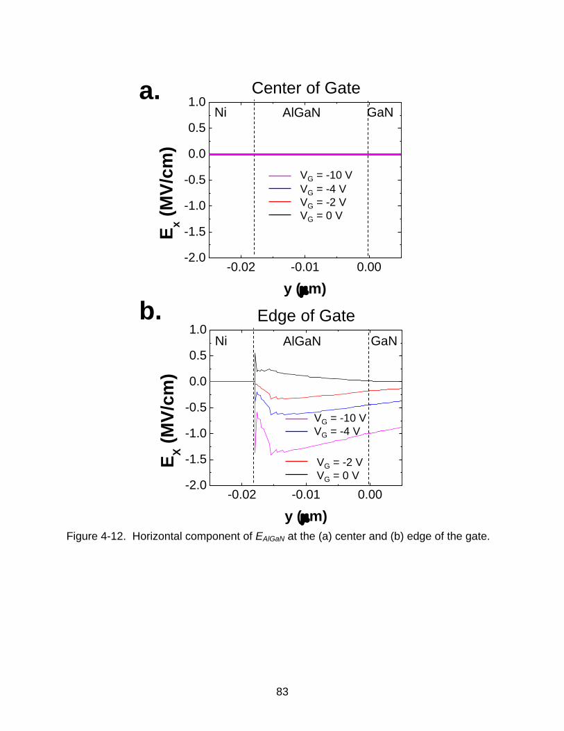
83
Figure 4-12. Horizontal component of EAlGaN at the (a) center and (b) edge of the gate.
a.
b.
Center of Gate
Edge of Gate
VG = -4 V
VG = -2 V
VG = 0 V
VG = -2 V
VG = 0 V
VG = -10 V
VG = -4 V
Ni AlGaN GaN
Ni AlGaN GaN
VG = -10 V
-0.02 -0.01 0.00-2.0
-1.5
-1.0
-0.5
0.0
0.5
1.0
Ex (
MV
/cm
)
y (m)
-0.02 -0.01 0.00-2.0
-1.5
-1.0
-0.5
0.0
0.5
1.0
EX (
MV
/cm
)
y (m)

84
CHAPTER 5 FIELD DEPENDENT MECHANICAL STRESS SENSITIVITY OF ALGAN/GAN HEMT
GATE LEAKAGE CURRENT
Introduction
AlGaN/GaN HEMTs provide benefits over Si, SiGe, SiC and GaAs material
systems for high frequency and high power applications. Unique advantages include a
built-in polarization and a wide bandgap which allow for high sheet charge carrier
density and high voltage operation. However, the device reliability of AlGaN/GaN
HEMTs still requires improvement. Particularly, generation of defects during high bias
operation has been shown to increase the gate leakage current density (JG), reducing
the output power and power added efficiency (PAE), limiting its prolonged usefulness in
high power applications [100]. A systematic study of gate leakage transport
mechanisms in the presence of defects is required.
The physical breakdown of the AlGaN barrier has been shown to occur at voltages
beyond the critical voltage (Vcrit), creating an irreversible increase in JG [11]. To
demonstrate this crucial AlGaN/GaN HEMT failure mode, a step voltage stress is
applied and the gate current is monitored. Figure 5-1 shows the results of VG step
electrical stress on JG at the VDS = 0 V state, showing a sudden increase in JG at Vcrit.
This type of degradation has been hypothesized to be related to the generation of
crystallographic defects via the inverse piezoelectric effect [11]. At large VG, as seen
from the Sentaurus 2D simulations in Chapter 4, increased vertical field occurs at the
gate edges. This creates additional tensile stress in the AlGaN barrier through the
inverse piezoelectric effect. This stress adds to the pre-existing built-in tensile stress
resulting from lattice mismatch between the AlGaN barrier and the GaN layer. It has
been suggested that when stress reaches the material critical limit, defect to form in
85
order to relax the internal elastic energy [11]. These defects cause a low resistance
leakage path through the AlGaN barrier resulting in a sudden increase in JG. A
mechanical wafer bending experiment in literature showed a reduction of Vcrit with
applied mechanical stress, however, only five pairs of devices were investigated in this
study and a more comprehensive study is required [101].
Since stress is inherent in AlGaN/GaN HEMTs, understanding the role of stress on
JG is essential to improve reliability. However, there are discrepancies in the published
literature explaining the gate leakage mechanism of unstressed devices. Several
transport mechanisms have been suggested to explain JG such as trap-assisted
tunneling [34], [78-81], direct or FN tunneling [78-80], [82], temperature assisted
tunneling[78], [83], multi-step trap-assisted tunneling [84], thermionic trap assisted
tunneling [82], [85-87], tunneling through a thin surface barrier [88], and PF emission
[89-94]. We endeavor to resolve the mechanisms of gate leakage in AlGaN/GaN HEMT
by varying external mechanical stress and reverse gate bias simultaneously, and
discuss implications on the effect of mechanical stress on device degradation.
Experiment
Wafer samples were attached to heat-treated high-carbon steel plates with epoxy
and stressed in a four-point wafer bending setup. Compressive and tensile uniaxial
stress up to 360 MPa was applied longitudinal to the channel direction. The stress
dependence of the AlGaN/GaN HEMT JG was characterized at the VDS = 0 state,
isolating the effect of electric field induced by the gate. Various reverse biases (-0.1 V
to -4 V) were applied to the gate and held constant until JG reached steady-state to
eliminate transient trapping effects before each measurement. At each bias,
mechanical stress was incrementally applied then released, while simultaneously
86
measuring JG. High-temperature measurements were taken on a temperature-
controlled probe station using sample stage heaters.
Results and Discussion
Wafer Bending Results
Longitudinal stress, up to 360 MPa, was incrementally applied to the AlGaN/GaN
HEMT device while JG was simultaneously measured over a period of 1800 seconds.
Averaging JG over 1800 seconds was done to account for random fluctuations in the
measured current. It was found that a time duration of 1800 seconds while the stress
was held constant was adequate to obtain a reasonable statistical confidence in the
measured JG. The normalized change in JG due to applied stress (ΔJG(σ)/JG(0)) was
measured for several constant applied gate biases (VG = -0.1, -0.25, -0.5, -1, -2, and -4
V) using the above mentioned procedure. Figure 5-2 shows results of ΔJG(σ)/JG(0) for
VG = -0.25 V and -4 V. The stress dependence of JG was weaker at VG = -4 V than at
VG = -0.25 V. Tensile (compressive) stress increased (decreased) JG for all applied
gate biases. At each bias, after the compressive or tensile stress was applied to its
maximum magnitude of 360 MPa, then the stress was incrementally released. Upon
releasing the stress to zero, JG returned to its initial, unstressed value. This
demonstrates that the measured change in JG is purely a reversible consequence of the
applied stress, and not a transient effect. Also, it demonstrates that the applied
mechanical stress (up to 360 MPa) does not induce permanent damage to the device.
To quantify the magnitude of the normalized change in gate current density,
ΔJG(σ)/JG(0), for each applied gate bias and stress level, JG is averaged over the
duration of time the stress was held constant. Figure 5-3 shows ΔJG(σ)/JG(0) averaged
for all levels of compressive and tensile stress at VG = -0.25 V and -4 V. Error bars
87
representing the uncertainty in the measurement of ΔJG(σ)/JG(0) are three times the
standard deviation of the JG measurements over the duration when the stress was held
constant.
The sensitivity of JG to stress defined as the normalized change in JG per stress,
[ΔJG(σ)/JG(0)]/σ, is calculated from the slope of the weighted total least squares linear fit
of ΔJG(σ)/JG(0) versus stress, including uncertainty in JG at each stress increment. The
stress sensitivity of JG is plotted as a function of reverse gate bias in Figure 5-4.
Increasing the reverse gate bias is observed to decrease the sensitivity of JG to stress.
The sensitivity of JG to stress decreased from 1.7 ±0.3 %/100MPa at VG = -0.25 V to 0.6
±0.1 %/100MPa at VG = -4 V as shown in Figure 5-4. To interpret the decreasing
sensitivity for increasing reverse gate bias, the dominant gate leakage transport
mechanism needs to be analyzed.
Discussion
To understand the decreasing stress dependence of JG with increasing reverse
gate bias and compare the measurements to gate leakage transport models, the
experimentally determined 1D EAlGaN values discussed in Chapter 4 are used. Since the
2D edge effects complicate the EAlGaN profile under the gate for gate biases below VT,
the simple 1D model cannot be used. Therefore, we analyze the gate leakage
mechanism only for VG above VT. Simulations performed indicate that thermionic
emission, bulk trap assisted tunneling, and Fowler-Nordheim (FN) tunneling models
underestimate the magnitude of the experimental data [102]. However, the Poole-
Frenkel (PF) emission model for gate leakage current closely matches the experimental
data.

88
PF emission refers to the lowering of the Coulombic potential barrier of a trapped
electron due to a large electric field, increasing the probability for the electron to be
emitted into the conduction band. The general expression for PF emission current
considering compensation is [103-105]:
*
√
+ (5-1)
where,
√
(5-2)
C is a constant related to mobility and density of states, EA is the trap activation energy,
is the vacuum permittivity, and is the relative permittivity of the AlGaN. The
compensation, or slope parameter, r ranges from 1 to 2 depending on the amount of
acceptor concentration and position of the Fermi energy with respect to EA [103-105].
This compensation parameter is used as a first order model parameter to describe
acceptor compensation. Often, the assumption of r = 1 is used to model PF emission
data [93], [94]. When r =1, the concentration of electrons excited up to the conduction
band is small relative to the donor and acceptor densities. When r = 2, the
concentration of acceptor levels is small compared to the number of donor levels and
excited electrons. The EA extracted from the PF model represents the average trap
energy level with respect to the conduction band of the traps contributing to PF current.
Traps are distributed both in energy and space throughout the AlGaN barrier; the
extracted EA only represents the traps participating in emitting electrons to the
conduction band via the PF effect. Also, the trap levels are assumed to be located
89
physically close to the top surface of the AlGaN layer, under the gate, therefore the
traps are assumed to be filled, and only the emission is considered.
To determine the dominate gate leakage mechanism of the experimentally
measured devices, the JG versus VG curves (Figure 5-5) were measured from 300 K to
400K. Since PF emission is a thermal assisted process whose efficiency increases at
higher temperatures, the gate current was measured at temperatures larger room
temperature. The temperature and field dependence of JG were plotted in a PF plot
(plot of the natural logarithm of the gate current divided by the electric field versus
square root of the electric field) as shown in Figure 5-6. When plotted in this manner,
the linear region of the PF plot signifies that PF emission dominates the gate leakage
for that range of EAlGaN.
By taking the natural log of Equation 5-1, the PF equation can be written as a
linear equation, y = m(T)x +b(T). The slope and y-intercept of the PF plot are m(T) and
b(T) respectively.
(
)
√
(5-3)
( )
(5-4)
( )
(5-5)
To analyze the stress results systematically, the data is assumed to fit the PF
model beginning with an assumption of the limiting case of high compensation, when r =
1 independent of stress. Then, a more physical fit to the PF model is used where r is
determined by adjusting for a realistic value of the high frequency permittivity. Finally, a

90
reverse tunneling current is included into the overall expression to satisfy the equilibrium
condition, JG(VG = 0) = 0.
Maximum compensation (r = 1)
We begin the analysis by assuming the simple case, where the maximum acceptor
compensation level in the PF model is assumed (r = 1). The permittivity is extracted
including the entire range of measured temperatures (T = 300 K to 400 K). First, the
slope of the PF plot is plotted against 1/T (Figure 5-7). The slope of the linear fit to the
plot in Figure 5-7 with the y-intercept forced to zero (m’), is
√
(5-6)
Then, the permittivity is calculated from
(5-7)
giving a value of 5.88. Including the uncertainty in the measured JG of 3.3% from a
control measurement of 1200 simultaneous measurements, the uncertainty in the
extracted value of is determined by including the error in the linear fit when
calculating m’. The resulting uncertainty in is approximately ±0.16. So, for r = 1,
= 5.88 ±0.16.
Then, the trap activation energy is extracted using the y-intercept of the PF plot
(Equation 5-5). First, the y-intercept of the PF plot is plotted against 1/T (Figure 5-8).
The value of EA is calculated from the slope (m’’), and ln(C) is the y-intercept of the
linear fit to the plot in Figure 5-8, where
(5-9)
91
Hence,
(5-10)
EA was determined to be 0.37 eV and ln(C) = -14.23. The uncertainty in EA and ln(C) is
estimated by including the uncertainty of the linear fit when obtaining m’’. This gives an
estimate for the error of ±0.05 eV for EA and ±1.55 for ln(C).
The stress dependence of the PF current can be derived by first defining the
unstressed PF current for r = 1 as:
( ) (
√
) (5-11)
In the PF expression, only EA is assumed to be affected by mechanical stress. Stress
has been known to change the trap activation energy level in Si/HfSiON devices
dominated by PF tunneling through altering bond angle and lengths [106][107].
Although the nature of the trap is likely different in the AlGaN/GaN system than
Si/HfSiON, similar physics will apply where stress changes the bond lengths and
angles, which will in turn affect the trap activation energy. The compensation
parameter, permittivity, and other parameters are assumed to remain independent of
stress. During four-point bending, equal stress is applied to both the AlGaN and GaN
layer since the AlGaN/GaN interface is located close to the top surface of the wafer, far
from the neutral axis of bending. Therefore, EAlGaN will not be affected by the externally
applied stress. Under these assumptions, the PF current under stress is given by
( ) (
( ) √
) ( ) (
( )
) (5-12)
92
where ΔEA(σ) is the change in trap energy level due to the applied mechanical
stress. The normalized change in PF current with stress is:
( )
( )
( ) ( )
( ) (
( )
) (5-13)
Based on Equation 5-13, the expected normalized change in PF current for a
given amount of stress is constant independent of EAlGaN or VG. However, the
experimentally measured [ΔJG(σ)/JG(0)]/σ from wafer bending experiments decreases
with increasing reverse gate bias. Therefore, the simplistic model (r = 1 independent of
stress) fails to capture the correct trend observed experimentally.
Reduced compensation (1 < r < 2)
The permittivity used in the PF model should be the high frequency permittivity
[103]. This is because the trapping/detrapping effects are quick transients. The high
frequency permittivity of AlGaN is = 5.1 ±0.5, based on the high frequency
permittivities of AlN (4.6) and GaN (5.3) [108]. However, the value of permittivity
extracted from the PF model assuming the high compensation case with r = 1 was 5.88
±0.16. Since the extracted permittivity based on the assumption that r = 1 does not
match the required high permittivity value, the compensation factor r is adjusted. From
Equation 5-4 using = 5.1, the value r = 1.07 ±0.02 is extracted in order to provide
a more physical fit to the PF model. This value of r still signifies very high
compensation. Since the r value is adjusted to match the high frequency permittivity of
AlGaN, the EA value is also adjusted. Based on Equation 5-5 including r = 1.07 ±0.02,
the value of EA becomes 0.40 ±0.05 eV and ln(C) is -13.55 ±1.55.
Since r is no longer fixed at the limit of maximum compensation, when EA changes
with stress, r also will change with stress. Figure 5-9 shows a schematic of the trap
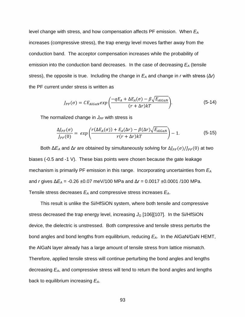
93
level change with stress, and how compensation affects PF emission. When EA
increases (compressive stress), the trap energy level moves farther away from the
conduction band. The acceptor compensation increases while the probability of
emission into the conduction band decreases. In the case of decreasing EA (tensile
stress), the opposite is true. Including the change in EA and change in r with stress (Δr)
the PF current under stress is written as
( ) (
( ) √
( ) ) (5-14)
The normalized change in JPF with stress is
( )
( ) (
( ( )) ( ) ( )√
( ) ) (5-15)
Both ΔEA and Δr are obtained by simultaneously solving for ( ) ( ) at two
biases (-0.5 and -1 V). These bias points were chosen because the gate leakage
mechanism is primarily PF emission in this range. Incorporating uncertainties from EA
and r gives ΔEA = -0.26 ±0.07 meV/100 MPa and Δr = 0.0017 ±0.0001 /100 MPa.
Tensile stress decreases EA and compressive stress increases EA.
This result is unlike the Si/HfSiON system, where both tensile and compressive
stress decreased the trap energy level, increasing JG [106][107]. In the Si/HfSiON
device, the dielectric is unstressed. Both compressive and tensile stress perturbs the
bond angles and bond lengths from equilibrium, reducing EA. In the AlGaN/GaN HEMT,
the AlGaN layer already has a large amount of tensile stress from lattice mismatch.
Therefore, applied tensile stress will continue perturbing the bond angles and lengths
decreasing EA, and compressive stress will tend to return the bond angles and lengths
back to equilibrium increasing EA.
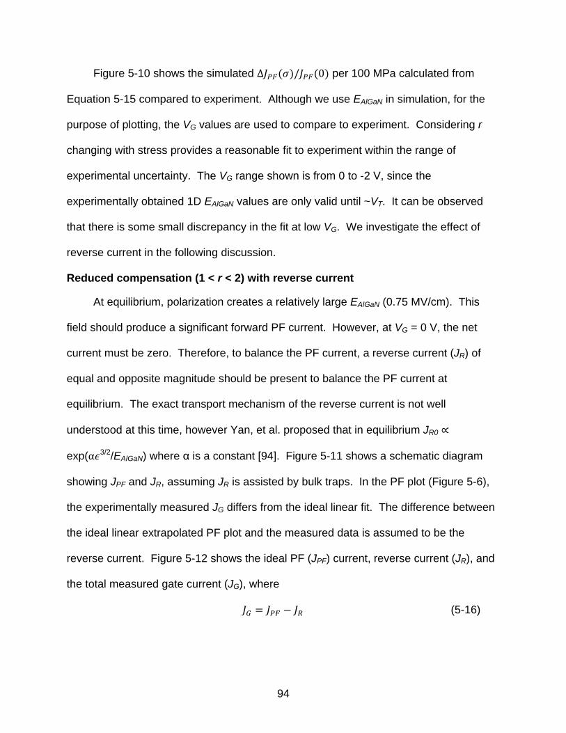
94
Figure 5-10 shows the simulated ( ) ( ) per 100 MPa calculated from
Equation 5-15 compared to experiment. Although we use EAlGaN in simulation, for the
purpose of plotting, the VG values are used to compare to experiment. Considering r
changing with stress provides a reasonable fit to experiment within the range of
experimental uncertainty. The VG range shown is from 0 to -2 V, since the
experimentally obtained 1D EAlGaN values are only valid until ~VT. It can be observed
that there is some small discrepancy in the fit at low VG. We investigate the effect of
reverse current in the following discussion.
Reduced compensation (1 < r < 2) with reverse current
At equilibrium, polarization creates a relatively large EAlGaN (0.75 MV/cm). This
field should produce a significant forward PF current. However, at VG = 0 V, the net
current must be zero. Therefore, to balance the PF current, a reverse current (JR) of
equal and opposite magnitude should be present to balance the PF current at
equilibrium. The exact transport mechanism of the reverse current is not well
understood at this time, however Yan, et al. proposed that in equilibrium JR0
exp(α 3/2/EAlGaN) where α is a constant [94]. Figure 5-11 shows a schematic diagram
showing JPF and JR, assuming JR is assisted by bulk traps. In the PF plot (Figure 5-6),
the experimentally measured JG differs from the ideal linear fit. The difference between
the ideal linear extrapolated PF plot and the measured data is assumed to be the
reverse current. Figure 5-12 shows the ideal PF (JPF) current, reverse current (JR), and
the total measured gate current (JG), where
(5-16)
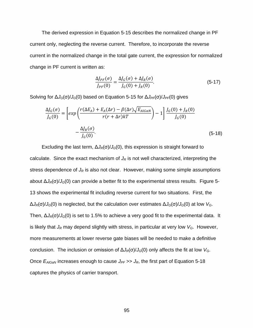
95
The derived expression in Equation 5-15 describes the normalized change in PF
current only, neglecting the reverse current. Therefore, to incorporate the reverse
current in the normalized change in the total gate current, the expression for normalized
change in PF current is written as:
( )
( )
( ) ( )
( ) ( ) (5-17)
Solving for ΔJG(σ)/JG(0) based on Equation 5-15 for ΔJPF(σ)/JPF(0) gives
( )
( ) * (
( ) ( ) ( )√
( ) ) +
( ) ( )
( )
( )
( )
(5-18)
Excluding the last term, ΔJR(σ)/JG(0), this expression is straight forward to
calculate. Since the exact mechanism of JR is not well characterized, interpreting the
stress dependence of JR is also not clear. However, making some simple assumptions
about ΔJR(σ)/JG(0) can provide a better fit to the experimental stress results. Figure 5-
13 shows the experimental fit including reverse current for two situations. First, the
ΔJR(σ)/JG(0) is neglected, but the calculation over estimates ΔJG(σ)/JG(0) at low VG.
Then, ΔJR(σ)/JG(0) is set to 1.5% to achieve a very good fit to the experimental data. It
is likely that JR may depend slightly with stress, in particular at very low VG. However,
more measurements at lower reverse gate biases will be needed to make a definitive
conclusion. The inclusion or omission of ΔJR(σ)/JG(0) only affects the fit at low VG.
Once EAlGaN increases enough to cause JPF >> JR, the first part of Equation 5-18
captures the physics of carrier transport.
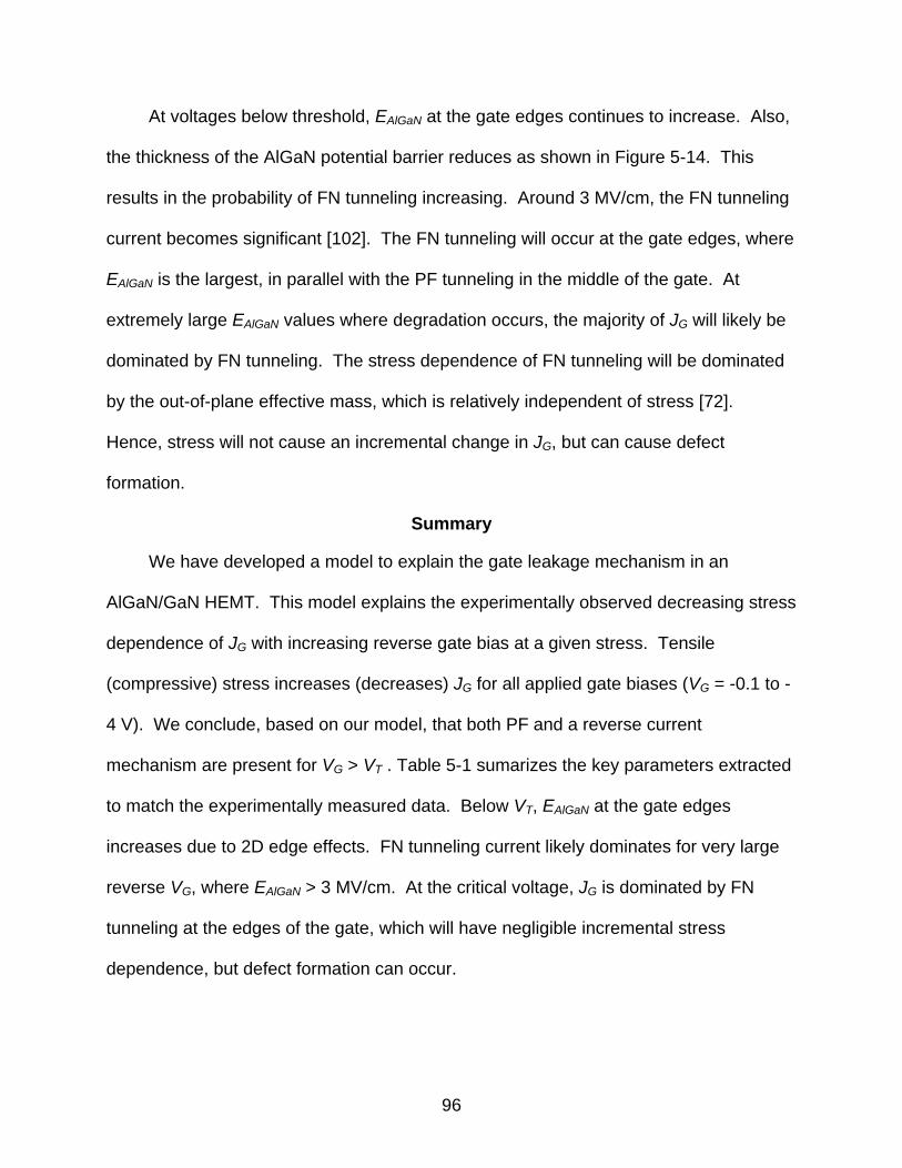
96
At voltages below threshold, EAlGaN at the gate edges continues to increase. Also,
the thickness of the AlGaN potential barrier reduces as shown in Figure 5-14. This
results in the probability of FN tunneling increasing. Around 3 MV/cm, the FN tunneling
current becomes significant [102]. The FN tunneling will occur at the gate edges, where
EAlGaN is the largest, in parallel with the PF tunneling in the middle of the gate. At
extremely large EAlGaN values where degradation occurs, the majority of JG will likely be
dominated by FN tunneling. The stress dependence of FN tunneling will be dominated
by the out-of-plane effective mass, which is relatively independent of stress [72].
Hence, stress will not cause an incremental change in JG, but can cause defect
formation.
Summary
We have developed a model to explain the gate leakage mechanism in an
AlGaN/GaN HEMT. This model explains the experimentally observed decreasing stress
dependence of JG with increasing reverse gate bias at a given stress. Tensile
(compressive) stress increases (decreases) JG for all applied gate biases (VG = -0.1 to -
4 V). We conclude, based on our model, that both PF and a reverse current
mechanism are present for VG > VT . Table 5-1 sumarizes the key parameters extracted
to match the experimentally measured data. Below VT, EAlGaN at the gate edges
increases due to 2D edge effects. FN tunneling current likely dominates for very large
reverse VG, where EAlGaN > 3 MV/cm. At the critical voltage, JG is dominated by FN
tunneling at the edges of the gate, which will have negligible incremental stress
dependence, but defect formation can occur.
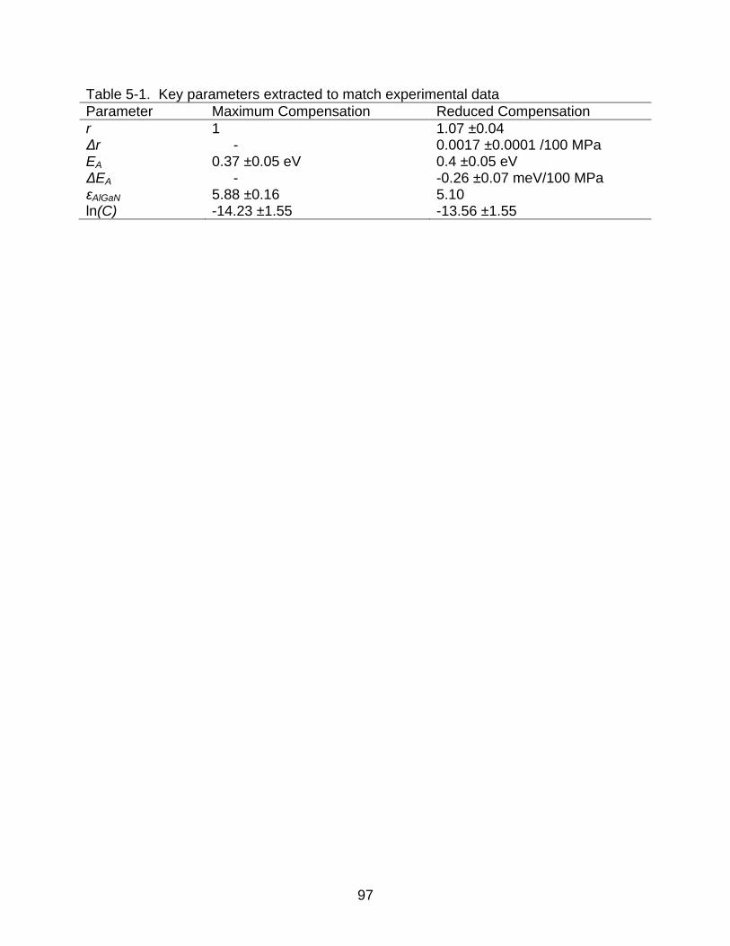
97
Table 5-1. Key parameters extracted to match experimental data
Parameter Maximum Compensation Reduced Compensation
r 1 1.07 ±0.04 Δr - 0.0017 ±0.0001 /100 MPa EA 0.37 ±0.05 eV 0.4 ±0.05 eV ΔEA - -0.26 ±0.07 meV/100 MPa εAlGaN 5.88 ±0.16 5.10 ln(C) -14.23 ±1.55 -13.56 ±1.55
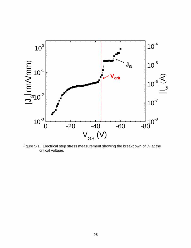
98
Figure 5-1. Electrical step stress measurement showing the breakdown of JG at the
critical voltage.
Vcrit
JG
0 -20 -40 -60 -8010
-3
10-2
10-1
100
|IG(
A)
VGS
(V)
|JG(
mA
/mm)
10-8
10-7
10-6
10-5
10-4
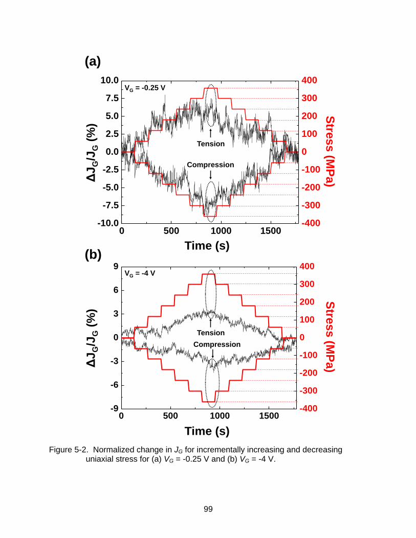
99
Figure 5-2. Normalized change in JG for incrementally increasing and decreasing
uniaxial stress for (a) VG = -0.25 V and (b) VG = -4 V.
0 500 1000 1500-9
-6
-3
0
3
6
9
-400
-300
-200
-100
0
100
200
300
400VG = -4 V
Compression
Tension
ΔJ
G/J
G(%
)S
tres
s (M
Pa)
Time (s)
(b)
VG = -0.25 V
Compression
Tension
0 500 1000 1500-10.0
-7.5
-5.0
-2.5
0.0
2.5
5.0
7.5
10.0
-400
-300
-200
-100
0
100
200
300
400
ΔJ
G/J
G(%
)S
tres
s (M
Pa)
Time (s)
(a)
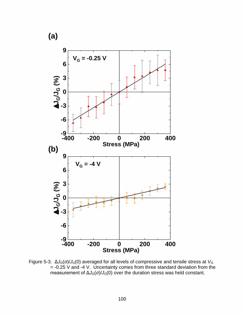
100
Figure 5-3. ΔJG(σ)/JG(0) averaged for all levels of compressive and tensile stress at VG
= -0.25 V and -4 V. Uncertainty comes from three standard deviation from the measurement of ΔJG(σ)/JG(0) over the duration stress was held constant.
-400 -200 0 200 400-9
-6
-3
0
3
6
9
JG
/JG
(%
)
Stress (MPa)
-400 -200 0 200 400-9
-6
-3
0
3
6
9
J
G/J
G (
%)
Stress (MPa)
VG = -4 V
VG = -0.25 V
(b)
(a)
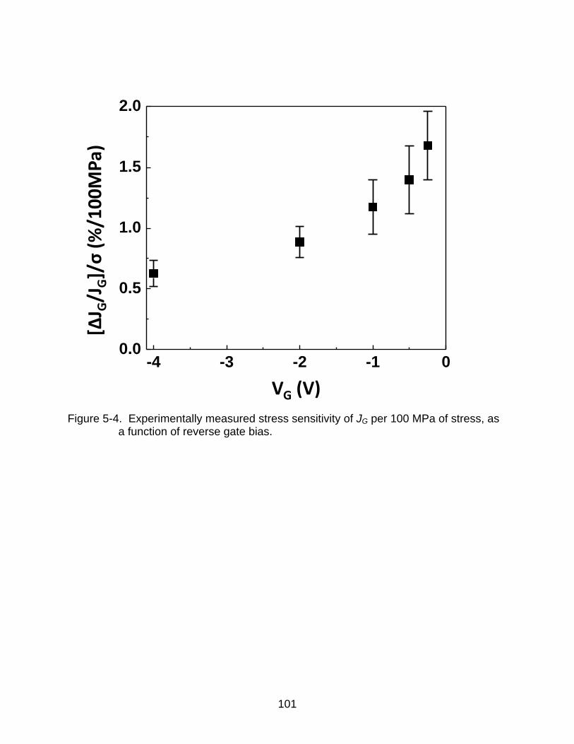
101
Figure 5-4. Experimentally measured stress sensitivity of JG per 100 MPa of stress, as
a function of reverse gate bias.
[ΔJ G
/JG]/σ
(%/1
00
MP
a)
VG (V)
-4 -3 -2 -1 00.0
0.5
1.0
1.5
2.0
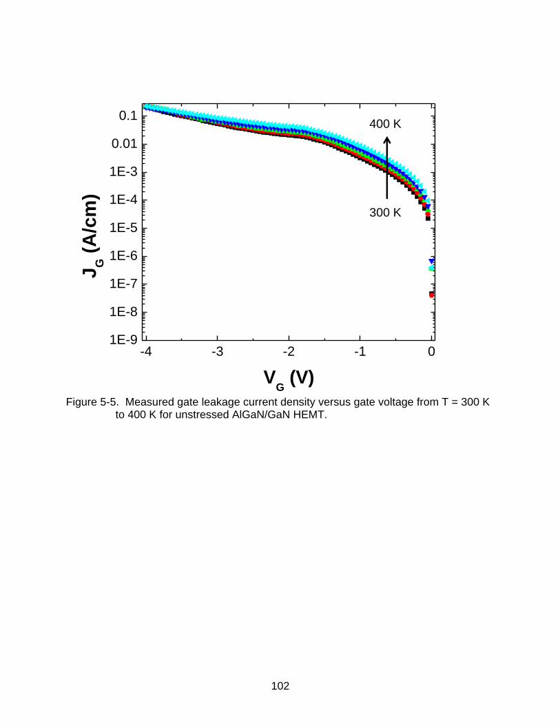
102
Figure 5-5. Measured gate leakage current density versus gate voltage from T = 300 K
to 400 K for unstressed AlGaN/GaN HEMT.
-4 -3 -2 -1 01E-9
1E-8
1E-7
1E-6
1E-5
1E-4
1E-3
0.01
0.1
J
G (
A/c
m)
VG (V)
400 K
300 K
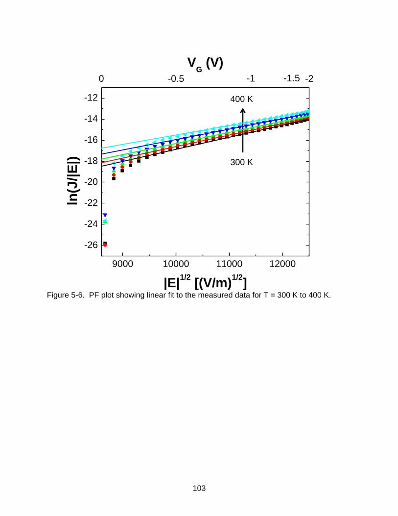
103
Figure 5-6. PF plot showing linear fit to the measured data for T = 300 K to 400 K.
400 K
300 K
9000 10000 11000 12000
-26
-24
-22
-20
-18
-16
-14
-12
-0.5 -1.5
ln(J
/|E
|)
|E|1/2
[(V/m)1/2
]
-10 -2
VG (V)
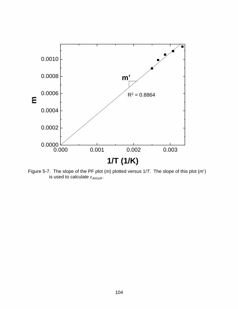
104
Figure 5-7. The slope of the PF plot (m) plotted versus 1/T. The slope of this plot (m’)
is used to calculate .
0.000 0.001 0.002 0.0030.0000
0.0002
0.0004
0.0006
0.0008
0.0010
m
1/T (1/K)
m’
R2 = 0.8864
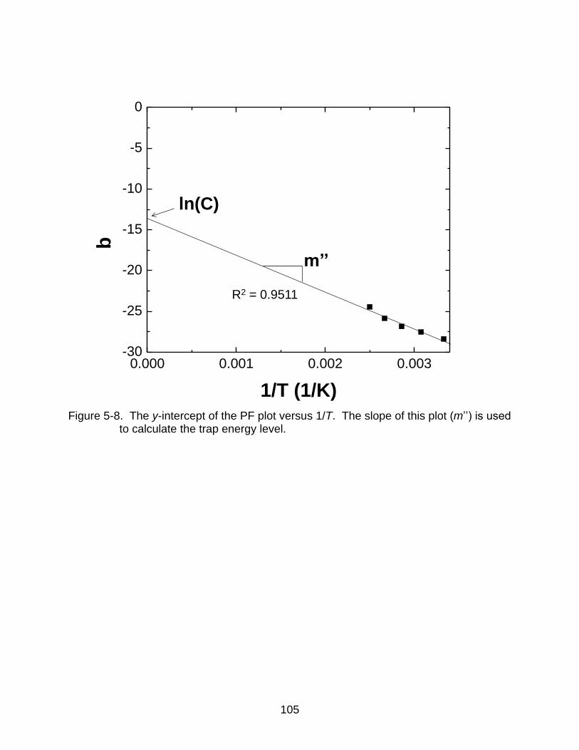
105
Figure 5-8. The y-intercept of the PF plot versus 1/T. The slope of this plot (m’’) is used
to calculate the trap energy level.
0.000 0.001 0.002 0.003-30
-25
-20
-15
-10
-5
0b
1/T (1/K)
m’’
ln(C)
R2 = 0.9511
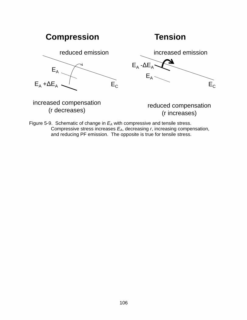
106
Figure 5-9. Schematic of change in EA with compressive and tensile stress.
Compressive stress increases EA, decreasing r, increasing compensation, and reducing PF emission. The opposite is true for tensile stress.
ECECEA +ΔEA
EA -ΔEA
Compression Tension
increased compensation
(r decreases)reduced compensation
(r increases)
EAEA
reduced emission increased emission
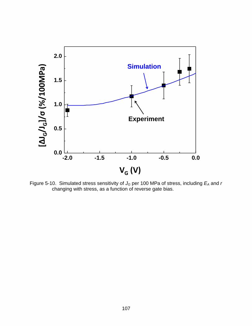
107
Figure 5-10. Simulated stress sensitivity of JG per 100 MPa of stress, including EA and r
changing with stress, as a function of reverse gate bias.
-2.0 -1.5 -1.0 -0.5 0.00.0
0.5
1.0
1.5
2.0
[ΔJ G
/JG]/σ
(%/1
00
MP
a)
VG (V)
Experiment
Simulation
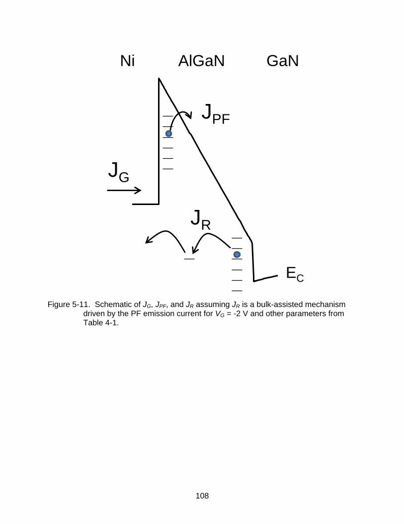
108
Figure 5-11. Schematic of JG, JPF, and JR assuming JR is a bulk-assisted mechanism
driven by the PF emission current for VG = -2 V and other parameters from Table 4-1.
JPF
JG
JR
EC
Ni AlGaN GaN
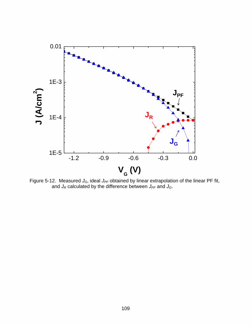
109
Figure 5-12. Measured JG, ideal JPF obtained by linear extrapolation of the linear PF fit,
and JR calculated by the difference between JPF and JG.
-1.2 -0.9 -0.6 -0.3 0.01E-5
1E-4
1E-3
0.01
J
(A
/cm
2)
VG (V)
JPF
JR
JG
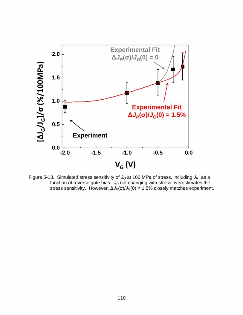
110
Figure 5-13. Simulated stress sensitivity of JG at 100 MPa of stress, including JR, as a
function of reverse gate bias. JR not changing with stress overestimates the stress sensitivity. However, ΔJR(σ)/JG(0) = 1.5% closely matches experiment.
[ΔJ G
/JG]/σ
(%/1
00
MP
a)
VG (V)
Experiment
Experimental Fit
ΔJR(σ)/JG(0) = 0
Experimental Fit
ΔJR(σ)/JG(0) = 1.5%
-2.0 -1.5 -1.0 -0.5 0.00.0
0.5
1.0
1.5
2.0
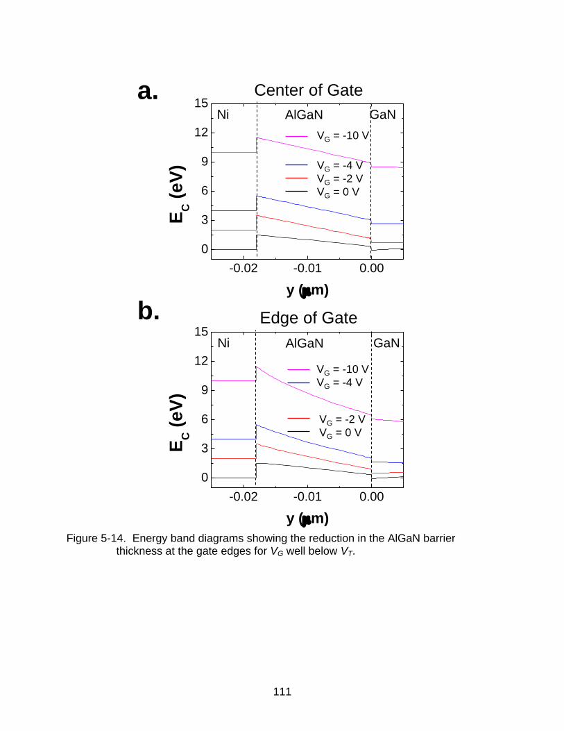
111
Figure 5-14. Energy band diagrams showing the reduction in the AlGaN barrier
thickness at the gate edges for VG well below VT.
-0.02 -0.01 0.00
0
3
6
9
12
15
EC (
eV
)
y (m)
-0.02 -0.01 0.00
0
3
6
9
12
15
EC (
eV
)
y (m)
Center of Gate
Edge of Gate
VG = -4 V
VG = -2 V
VG = 0 V
VG = -2 V
VG = 0 V
VG = -10 V
VG = -4 V
Ni AlGaN GaN
Ni AlGaN GaN
VG = -10 V
a.
b.
112
CHAPTER 6 CONCLUSION
Overall Summary
A systematic study of the effect of mechanical stress on AlGaN/GaN HEMTs was
presented in this dissertation. Stress is inherent to AlGaN/GaN HEMTs, and can be
beneficial or detrimental to performance and reliability. The lattice mismatch stress
between AlGaN and GaN benefits the device by creating the 2DEG inducing
polarization, while stress generated via the inverse piezoelectric effect can induce
degradation. To characterize the impact of stress on the performance and reliability of
AlGaN/GaN HEMTs, a novel technique was developed to apply external stress to small
(~1 cm2) wafer samples while simultaneously taking electrical measurements. A four-
point wafer bending setup applied stress to the small sample, which was attached to a
high carbon stainless steel strip with epoxy. To simultaneously conduct electrical
measurements while varying the amount of mechanical stress, wires were attached to
the bond pads with room temperature curing conductive epoxy.
An enormous variation in AlGaN/GaN HEMT gauge factor measurements (4 to -
40,000) have been reported in literature (E. Y. Chang, 2009; Eickhoff et al., 2001;
Gaska et al., 1998; Kang et al., 2005, 2004; Yilmazoglu et al., 2006; Zimmermann et al.,
2006) and is likely a result of charge trapping effects. After eliminating the charge
trapping effects, the measured gauge factor of the AlGaN/GaN HEMT was -2.8 ±0.4.
This gauge factor indicates a small stress dependence on the device resistivity. This is
explained by small changes in the 2DEG sheet carrier density and channel mobility.
The experimental results were compared with a simulated gauge factor (-7.9 ±5.2) to
determine the best fitting set of elastic and piezoelectric coefficients of GaN and AlN.
113
In order to determine the dominant gate leakage mechanism, a thorough
investigation of the relationship between EAlGaN and VG was presented. In a simple
model of an ideal 1D device, EAlGaN has a linear relationship to VG above VT, and
saturates below VT. Experimentally determined parameters were used in the 1D
calculation to model the actual device. Adjusting σint and ns based on experimental
measurements provided an accurate VG versus EAlGaN relationship above threshold.
Also, a comprehensive 2D simulation was performed to provide insight on EAlGaN for
large reverse biases much below VT. The 2D results proved the 1D model accurate for
VG > VT. However, below threshold, although EAlGaN saturates in the middle of the gate,
at the gate edges, EAlGaN continues to increase.
PF conduction was proven to be the dominant gate leakage transport mechanism
above threshold. Bias and stress dependence of JG was measured simultaneously. A
decreasing stress dependence of JG with increasing reverse gate bias was observed.
Tensile (compressive) stress increases (decreases) JG for all applied gate biases (VG =
-0.1 to -4 V). Compressive stress increases EA, and tensile stress decreases EA. Since
stress shifts the trap energy level, the compensation parameter r is also affected by
stress. A reverse tunneling current was included in the model to balance the forward
PF current at equilibrium. However, the reverse tunneling current only is important at
extremely small gate biases. At very large increasing reverse biases, EAlGaN at the gate
edges continues to increase, which decreases the tunneling barrier making FN
tunneling more probable. When degradation occurs, the contribution to JG is dominated
by FN tunneling at the edges of the gate.
114
Future Work
Mechanical stress has been shown to affect AlGaN/GaN HEMT channel
resistance and gate current. The demand for improved performance and reliability of
AlGaN/GaN HEMT devices requires further analysis into the role of mechanical stress in
degradation.
A more comprehensive understanding of the reverse tunneling current will help to
understand how stress affects the gate leakage current at very low reverse biases.
More measurements of ΔJG(σ)/JG(0) data points need to be obtained at low bias (-0.1 V
< VG 0 V) to see if reverse tunneling current is present, and if it has a stress
dependence.
Also, degradation experiments combining the effects of temperature, electrical
stress, light, and mechanical stress will provide further insight into the role of
mechanical stress on device degradation. Since limitations on samples prevent a
thorough statistical degradation investigation, experiments need to be designed to
isolate the effect of stress on degradation. Gate current should be monitored to
evaluate degradation as the device is incrementally stressed using temperature and
electrical stress just prior to breakdown. Then, mechanical tensile stress can be applied
to attempt to induce degradation. Then, a more direct relationship between stress and
device failure can be obtained.
Also, trap characterization under mechanical stress to directly measure the
change in trap energy with stress will be extremely beneficial. Using optical trap
characterization methods will be best since there is no body contact in the AlGaN/GaN
HEMT devices making other characterization methods invalid. A more direct

115
measurement of the effect of stress on AlGaN/GaN HEMT traps can help to engineer
more reliable, better performing devices.
116
LIST OF REFERENCES
[1] T. Mimura, S. Hiyamizu, T. Fujii, and K. Nanbu, “A New Field-Effect Transistor with Selectively Doped GaAs/n-AlxGa1- xAs Heterojunctions,” Japanese Journal of Applied Physics, vol. 19, no. 5. p. L225-L227, May-1980.
[2] T. Mimura, “The Early History of the High Electron Mobility Transistor (HEMT),” IEEE Transactions on Microwave Theory and Techniques, vol. 50, no. 3, pp. 780-782, Mar. 2002.
[3] M. Asif Khan, A. Bhattarai, J. N. Kuznia, and D. T. Olson, “High Electron Mobility Transistor Based on a GaN-AlxGa1-xN Heterojunction,” Applied Physics Letters, vol. 63, no. 9, p. 1214, 1993.
[4] R. J. Trew, “High-Frequency Solid-State Electronic Devices,” IEEE Transactions on Electron Devices, vol. 52, no. 5, pp. 638-649, May. 2005.
[5] P. Rajagopal, T. Gehrke, and J. Roberts, “Large-Area, Device Quality GaN on Si Using a Novel Transition Layer Scheme,” Mater. Res. Soc. Symp. Proc, vol. 1, no. 1, pp. 6-11, 2003.
[6] Cree inc., CGH31240F 240 W, 2700-3100 MHz, 50-ohm Input/Output Matched, GaN HEMT for S-Band Radar Systems. 2011.
[7] Cree inc, CMPA2735075F 75 W, 2.7 - 3.5 GHz, GaN MMIC, Power Amplifier. 2011.
[8] Y. Hao, S. Member, L. Yang, X. Ma, J. Ma, and A. A. Gan, “High-Performance Microwave Gate-Recessed,” Power, vol. 32, no. 5, pp. 626-628, 2011.
[9] O. Ambacher, J. Smart, J. R. Shealy, N. G. Weimann, K. Chu, M. Murphy, W. J. Schaff, L. F. Eastman, R. Dimitrov, L. Wittmer, M. Stutzmann, W. Rieger, and J. Hilsenbeck, “Two-Dimensional Electron Gases Induced by Spontaneous and Piezoelectric Polarization Charges in N-and Ga-face AlGaN/GaN Heterostructures,” Journal of Applied Physics, vol. 85, no. 6, p. 3222, 1999.
[10] D. Gregusova, J. Bernat, M. Drzik, M. Marso, J. Novak, F. Uherek, and P. Kordos, “Influence of Passivation Induced Stress on the Performance of AlGaN/GaN HEMTs,” Physica Status Solidi (C), vol. 2, no. 7, pp. 2619-2622, May. 2005.
[11] J. Joh and J. A. del Alamo, “Critical Voltage for Electrical Degradation of GaN High-Electron Mobility Transistors,” IEEE Electron Device Letters, vol. 29, no. 4, pp. 287-289, Apr. 2008.
[12] S. Beeby, MEMS Mechanical Sensors. 2004.
[13] J. Bardeen and W. Shockley, “Deformation Potentials and Mobilities in Non-Polar Crystals,” Physical Review, vol. 80, no. 1, pp. 72-80, Oct. 1950.
117
[14] C. S. Smith, “Piezoresistance Effect in Germanium and Silicon,” Physical Review, vol. 94, no. 1, p. 42, 1954.
[15] Y. Sun, S. Thompson, and T. Nishida, Strain Effect in Semiconductors Theory and Device Applications. 2010.
[16] A. People, J. C. Bean, D. V. Lang, A. M. Sergent, H. L. Stormer, K. W. Wecht, R. T. Lynch, and K. Baldwin, “Modulation Doping in GexSi1-x/Si Strained Layer Heterostructure,” Applied Physics Letters, vol. 45, no. 11, pp. 1231-1233, May. 1984.
[17] H. M. Manasevit, “Electron Mobility Enhancement in Epitaxial Multilayer Si-Si1−xGex Alloy Films on (100) Si,” Applied Physics Letters, vol. 41, no. 5, p. 464, 1982.
[18] M. L. Lee and E. a Fitzgerald, “Hole Mobility Enhancements in Nanometer-Scale Strained-Silicon Heterostructures Grown on Ge-Rich Relaxed Si1−xGex,” Journal of Applied Physics, vol. 94, no. 4, p. 2590, 2003.
[19] K. Rim, S. Koester, M. Hargrove, J. Chu, P. M. Mooney, J. Ott, T. Kanarsky, P. Ronsheim, M. Ieong, A. Grill, and H.-S. P. Wong, “Strained Si NMOSFETs for High Performance CMOS Technology,” 2001 Symposium on VLSI Technology. Digest of Technical Papers (IEEE Cat. No.01 CH37184), pp. 59-60, 2001.
[20] S. Thompson, N. Anand, M. Armstrong, C. Auth, B. Arcot, M. Alavi, P. Bai, J. Bielefeld, R. Bigwood, J. Brandenburg, and others, “A 90 nm Logic Technology Featuring 50 nm Strained Silicon Channel Transistors, 7 Layers of Cu Interconnects, low k ILD, and 1 um2 SRAM Cell,” in Electron Devices Meeting, 2002. IEDM’02. Digest. International, 2002, pp. 61–64.
[21] S. E. Thompson, M. Armstrong, C. Auth, M. Alavi, M. Buehler, R. Chau, S. Cea, T. Ghani, G. Glass, T. Hoffman, C.-H. Jan, C. Kenyon, J. Klaus, K. Kuhn, Z. Ma, B. Mcintyre, K. Mistry, a Murthy, B. Obradovic, R. Nagisetty, P. Nguyen, S. Sivakumar, R. Shaheed, L. Shifren, B. Tufts, S. Tyagi, M. Bohr, and Y. El-Mansy, “A 90-nm Logic Technology Featuring Strained-Silicon,” IEEE Transactions on Electron Devices, vol. 51, no. 11, pp. 1790-1797, Nov. 2004.
[22] S. E. Thompson, M. Armstrong, C. Auth, S. Cea, R. Chau, G. Glass, T. Hoffman, J. Klaus, Z. Ma, B. Mcintyre, a Murthy, B. Obradovic, L. Shifren, S. Sivakumar, S. Tyagi, T. Ghani, K. Mistry, M. Bohr, and Y. El-Mansy, “A Logic Nanotechnology Featuring Strained-Silicon,” IEEE Electron Device Letters, vol. 25, no. 4, pp. 191-193, Apr. 2004.
[23] H. Yang, R. Malik, S. Narasimha, Y. Li, R. Divakaruni, P. Agnello, S. Allen, A. Antreasyan, J. Arnold, K. Bandy, and others, “Dual stress liner for high performance sub-45nm gate length SOI CMOS manufacturing,” in Electron Devices Meeting, 2004. IEDM Technical Digest. IEEE International, 2004, pp. 1075–1077.
118
[24] a Sozza, a Curutchet, C. Dua, N. Malbert, N. Labat, and a Touboul, “AlGaN/GaN HEMT Reliability Assessment by means of Low Frequency Noise Measurements,” Microelectronics and Reliability, vol. 46, no. 9-11, pp. 1725-1730, Sep. 2006.
[25] N. Sghaier, M. Trabelsi, N. Yacoubi, J. Bluet, A. Souifi, G. Guillot, C. Gaquiere, and J. Dejaeger, “Traps Centers and Deep Defects Contribution in Current Instabilities for AlGaN/GaN HEMT’s on Silicon and Sapphire Substrates,” Microelectronics Journal, vol. 37, no. 4, pp. 363-370, Apr. 2006.
[26] H. Rao and G. Bosman, “Device Reliability Study of High Gate Electric Field Effects in AlGaN/GaN High Electron Mobility Transistors Using Low Frequency Noise Spectroscopy,” Journal of Applied Physics, vol. 108, no. 5, p. 053707, 2010.
[27] W. Kruppa, S. Binari, and K. Doverspike, “Low-frequency Dispersion Characteristics of GaN HFETs,” Electronics Letters, vol. 31, no. 22, pp. 1951–1952, 1995.
[28] M. a Khan, M. S. Shur, and Q. C. Chen, “Current/Voltage Characteristic Collapse in AlGaN/GaN Heterostructure Insulated Gate Field Effect Transistors at High Drain Bias,” Electronics Letters, vol. 30, no. 25, p. 2175, 1994.
[29] J. Joh and J. D. Alamo, “A Simple Current Collapse Measurement Technique for GaN High-Electron Mobility Transistors,” Electron Device Letters, IEEE, vol. 29, no. 7, pp. 665-667, 2008.
[30] S. C. Binari, W. Kruppa, D. H. B., G. Kelnder, A. E. Wickenden, and J. A. Freitas, “Fabrication and Characterization of GaN FETs,” Solid-State Electronics, vol. 41, no. 10, pp. 1549-1554, Apr. 1997.
[31] S. Trassaert, B. Boudart, and C. Gaquiere, “Trap Effects Studies in GaN MESFETs by Pulsed Measurements,” Electronics, vol. 35, no. 16, pp. 1386-1388, 1999.
[32] S. C. Binari, K. Ikossi, J. a Roussos, W. Kruppa, H. B. Dietrich, D. D. Koleske, A. E. Wickenden, and R. L. Henry, “Trapping Effects and Microwave Power Performance in AlGaN/GaN HEMTs,” IEEE Transactions on Electron Devices, vol. 48, no. 3, pp. 465-471, Mar. 2001.
[33] G. Meneghesso, A. Chini, E. Zanoni, M. Manfredi, M. Pavesi, B. Boudart, and C. Gaquiere, “Diagnosis of Trapping Phenomena in GaN MESFETs,” International Electron Devices Meeting 2000. Technical Digest. IEDM (Cat. No.00CH37138), pp. 389-392.
[34] H. Kim, J. Lee, D. Liu, and W. Lu, “Gate Current Leakage and Breakdown Mechanism in Unpassivated AlGaN∕GaN High Electron Mobility Transistors by Post-Gate Annealing,” Applied Physics Letters, vol. 86, no. 14, p. 143505, 2005.
119
[35] J. Joh and J. a del Alamo, “Mechanisms for Electrical Degradation of GaN High-Electron Mobility Transistors,” 2006 International Electron Devices Meeting, pp. 1-4, Dec. 2006.
[36] S. Y. Son, Y. S. Choi, P. Kumar, H. W. Park, T. Nishida, R. K. Singh, and S. E. Thompson, “Strain Induced Changes in Gate Leakage Current and Dielectric Constant of Nitrided Hf-Silicate Metal Oxide Semiconductor Capacitors,” Applied Physics Letters, vol. 93, no. 15, p. 153505, 2008.
[37] S. Dey, M. Agostinelli, C. Prasad, X. Wang, and L. Shifren, “Effects of Hot Carrier Stress on Reliability of Strained-Si MOSFETs,” in Reliability Physics Symposium Proceedings, 2006. 44th Annual., IEEE International, 2006, pp. 461–464.
[38] S. Adachi, Handbook on Physical Properties of Semiconductors, vol. 1. 2004.
[39] M. Levinstein, S. Rumyantsev, and M. Shur, Handbook Series on Semiconductor Parameters. 1999.
[40] A. F. M. Anwar, S. Member, S. Wu, and R. T. Webster, “Temperature Dependent Transport Properties in GaN , AlxGa1-xN , and Inx Ga1-xN Semiconductors,” Transport, vol. 48, no. 3, pp. 567-572, 2001.
[41] R. Quay, “A Temperature Dependent Model for the Saturation Velocity in Semiconductor Materials,” Materials Science in Semiconductor Processing, vol. 3, no. 1-2, pp. 149-155, Mar. 2000.
[42] J. P. Ibbetson, P. T. Fini, K. D. Ness, S. P. DenBaars, J. S. Speck, and U. K. Mishra, “Polarization Effects, Surface States, and the Source of Electrons in AlGaN/GaN Heterostructure Field Effect Transistors,” Applied Physics Letters, vol. 77, no. 2, p. 250, 2000.
[43] J. W. Johnson, J. Gao, K. Lucht, J. Williamson, C. Strautin, J. Riddle, R. Therrien, P. Rajagopal, J. C. Roberts, A. Vescan, J. D. Brown, A. Hanson, S. Singhal, R. Borges, E. L. Piner, and K. J. Linthicum, “Material, Process, and Device Development of GaN-based HFETs on Silicon Substrates,” in Proc. Electrochem. Soc., 2004, vol. 3, no. 111, p. 405.
[44] S. Timoshenko, Strength of Materials. .
[45] K. Wu, “Strain Effects on the Valence Band of Silicon: Piezoresistance in P-type Silicon and Mobility Enhancement in Strained Silicon PMOSFET,” University of Florida, 2005.
[46] “GaN Esssentials - Substrates for GaN RF Devices,” 2008. [Online]. Available: www.nitronex.com.
120
[47] R. Gaska, J. W. Yang, a D. Bykhovski, M. S. Shur, V. V. Kaminski, and S. M. Soloviov, “The Influence of the Deformation on the Two-Dimensional Electron Gas Density in GaN–AlGaN Heterostructures,” Applied Physics Letters, vol. 72, no. 1, p. 64, 1998.
[48] M. Eickhoff, O. Ambacher, G. Kr tz, and M. Stutzmann, “Piezoresistivity of AlxGa1−xN Layers and AlxGa1−xN/GaN Heterostructures,” Journal of Applied Physics, vol. 90, no. 7, p. 3383, 2001.
[49] E. Y. Chang, “Changes of Electrical Characteristics for AlGaN/GaN HEMTs Under Uniaxial Tensile Strain,” IEEE Electron Device Letters, vol. 30, no. 3, pp. 213-215, Mar. 2009.
[50] T. Zimmermann, M. Neuburger, P. Benkart, F. J. Hernandez-Guillen, C. Pietzka, M. Kunze, I. Daumiller, A. Dadgar, A. Krost, and E. Kohn, “Piezoelectric GaN Sensor Structures,” IEEE Electron Device Letters, vol. 27, no. 5, pp. 309-312, May. 2006.
[51] O. Yilmazoglu, K. Mutamba, and D. Pavlidis, “Strain Sensitivity of AlGaN / GaN HEMT Structures for Sensing,” Engineer, no. 7, pp. 1037-1041, 2006.
[52] B. S. Kang, S. Kim, J. Kim, R. Mehandru, F. Ren, K. Baik, S. J. Pearton, B. P. Gila, C. R. Abernathy, C.-C. Pan, G.-T. Chen, J.-I. Chyi, V. Chandrasekaran, M. Sheplak, T. Nishida, and S. N. G. Chu, “AlGaN/GaN High Electron Mobility Transistor Structures for Pressure and pH Sensing,” Physica Status Solidi (C), vol. 2, no. 7, pp. 2684-2687, May. 2005.
[53] B. S. Kang, S. Kim, F. Ren, J. W. Johnson, R. J. Therrien, P. Rajagopal, J. C. Roberts, E. L. Piner, K. J. Linthicum, S. N. G. Chu, K. Baik, B. P. Gila, C. R. Abernathy, and S. J. Pearton, “Pressure-Induced Changes in the Conductivity of AlGaN∕GaN high-Electron Mobility-Transistor Membranes,” Applied Physics Letters, vol. 85, no. 14, p. 2962, 2004.
[54] R. Vetury, N. Q. Zhang, S. Keller, and U. K. Mishra, “The Impact of Surface States on the DC and RF Characteristics of AlGaN / GaN HFETs,” Measurement, vol. 48, no. 3, pp. 560-566, 2001.
[55] S. C. Binari, K. Ikossi, J. a Roussos, W. Kruppa, H. B. Dietrich, D. D. Koleske, A. E. Wickenden, and R. L. Henry, “Trapping Effects and Microwave Power Performance in AlGaN/GaN HEMTs,” IEEE Transactions on Electron Devices, vol. 48, no. 3, pp. 465-471, Mar. 2001.
[56] M. Gassoumi, J. Bluet, F. Chekir, I. Dermoul, H. Maaref, G. Guillot, A. Minko, V. Hoel, and C. Gaquiere, “Investigation of Traps in AlGaN/GaN HEMTs by Current Transient Spectroscopy,” Materials Science and Engineering: C, vol. 26, no. 2-3, pp. 383-386, Mar. 2006.
121
[57] A. D. Koehler, A. Gupta, M. Chu, S. Parthasarathy, K. J. Linthicum, J. W. Johnson, T. Nishida, and S. E. Thompson, “Extraction of AlGaN/GaN HEMT Gauge Factor in the Presence of Traps,” IEEE Electron Device Letters, vol. 31, no. 7, pp. 665-667, 2010.
[58] S. Bradley, A. Young, L. Brillson, M. Murphy, and W. Schaff, “Role of barrier and buffer layer defect states in AlGaN/GaN HEMT structures,” Journal of Electronic Materials, vol. 30, no. 3, pp. 123–128, 2001.
[59] H. Kim, A. Vertiatchikh, R. Thompson, V. Tilak, T. Prunty, J. Shealy, and L. Eastman, “Hot Electron Induced Degradation of Undoped AlGaN/GaN HFETs,” Microelectronics Reliability, vol. 43, no. 6, pp. 823-827, Jun. 2003.
[60] M. Chu, T. Nishida, X. Lv, N. Mohta, and S. E. Thompson, “Comparison Between High-Field Piezoresistance Coefficients of Si Metal-Oxide-Semiconductor Field-Effect Transistors and Bulk Si Under Uniaxial and Biaxial Stress,” Journal of Applied Physics, vol. 103, no. 11, p. 113704, 2008.
[61] O. Ambacher, “Two-Dimensional Electron Gases Induced by Spontaneous and Piezoelectric Polarization Charges in N-and Ga-face AlGaN/GaN Heterostructures,” Journal of Applied Physics, vol. 83, no. 6, p. 3656, 1999.
[62] A. Zoroddu, F. Bernardini, P. Ruggerone, and V. Fiorentini, “First-Principles Prediction of Structure, Energetics, Formation Enthalpy, Elastic Constants, Polarization, and Piezoelectric Constants of AlN, GaN, and InN: Comparison ofLocal and Gradient-Corrected Density-Functional Theory,” Physical Review B, vol. 64, no. 4, pp. 1-6, Jul. 2001.
[63] I. L. Guy, S. Muensit, E. M. Goldys, and D. Interna-, “Extensional Piezoelectric Coefficients of Gallium Nitride and Aluminum Nitride,” Applied Physics Letters, vol. 75, no. 26, pp. 4133-4135, 1999.
[64] K. Shimada, T. Sota, and K. Suzuki, “First-Principles Study on Electronic and Elastic Properties,” Journal of Applied Physics, vol. 84, no. 9, 1998.
[65] D. Vanderbilt, “Spontaneous Polarization and Piezoelectric Constants of III-V Nitrides,” Physical Review B, vol. 56, no. 16, pp. 24-27, 1997.
[66] A. Wright, “Elastic Properties of Zinc-Blende and Wurtzite AlN, GaN, and InN,” Journal of applied physics, vol. 82, no. September, p. 2833, 1997.
[67] A. Polian, M. Grimsditch, and I. Grzegory, “Elastic Constants of Gallium Nitride,” vol. 79, no. March, pp. 3343-3344, 1996.
[68] K. Kim, W. Lambrecht, and B. Segall, “Elastic constants and related properties of tetrahedrally bonded BN, AlN, GaN, and InN.,” Physical review. B, Condensed matter, vol. 53, no. 24, pp. 16310-16326, Jun. 1996.
122
[69] K. Kim, W. R. L. Lambrech, and B. Segall, “Electron Structure of GaN with Strain and Phonon Distorions,” Physical review. B, Condensed matter, vol. 50, Feb. 1994.
[70] E. Ruiz, S. Alvarez, and P. Alemany, “Electronic Structure and Properties of AlN.,” Physical review. B, Condensed matter, vol. 49, no. 11, pp. 7115-7123, Mar. 1994.
[71] T. Yang and S. Nakajima, “Electronic structures of Wurtzite GaN, InN and their alloy Ga1− xInxN calculated by the tight-binding method,” Japanese journal of applied physics, 1995.
[72] M. Chu, A. D. Koehler, A. Gupta, T. Nishida, and S. E. Thompson, “Simulation of AlGaN/GaN High-Electron-Mobility Transistor Gauge Factor Based on Two-Dimensional Electron Gas Density and Electron Mobility,” Journal of Applied Physics, vol. 108, no. 10, p. 104502, 2010.
[73] M. Yamaguchi, T. Yagi, T. Sota, T. Deguchi, K. Shimada, and S. Nakamura, “Brillouin scattering study of bulk GaN,” Journal of Applied Physics, vol. 85, no. 12, p. 8502, 1999.
[74] C. Deger, E. Born, H. Angerer, O. Ambacher, M. Stutzmann, J. Hornsteiner, E. Riha, and G. Fischerauer, “Sound Velocity of AlxGa1−xN Thin Films Obtained by Surface Acoustic-Wave Measurements,” Applied Physics Letters, vol. 72, no. 19. p. 2400, 1998.
[75] A. D. Bykhovski, V. V. Kaminski, M. S. Shur, Q. C. Chen, and M. A. Khan, “Piezoresistive Effect in Wurtzite n-type GaN,” Applied Physics Letters, vol. 68, no. 6. p. 818, 1996.
[76] K. Tsubouchi, “Zero Temperature Coefficient SAW Delay Line on AlN Epitaxial Films,” 1983 Ultrasonics Symposium, vol. 32, no. 5, p. 634, 1983.
[77] S. Mizuno, Y. Ohno, S. Kishimoto, K. Maezawa, and T. Mizutani, “Large Gate Leakage Current in AlGaN/GaN High Electron Mobility Transistors,” Japanese Journal of Applied Physics, vol. 41, no. Part 1, No. 8, pp. 5125-5126, Aug. 2002.
[78] S. Huang, B. Shen, F.-J. Xu, F. Lin, Z.-L. Miao, J. Song, L. Lu, L.-B. Cen, L.-W. Sang, Z.-X. Qin, Z.-J. Yang, and G.-Y. Zhang, “Study of the Leakage Current Mechanism in Schottky Contacts to Al 0.25 Ga 0.75 N/GaN Heterostructures with AlN Interlayers,” Semiconductor Science and Technology, vol. 24, no. 5, p. 055005, May. 2009.
[79] S. Karmalkar, D. M. Sathaiya, and M. S. Shur, “Mechanism of the Reverse Gate Leakage in AlGaN/GaN High Electron Mobility Transistors,” Applied Physics Letters, vol. 82, no. 22, p. 3976, 2003.
123
[80] E. J. Miller, E. T. Yu, P. Waltereit, and J. S. Speck, “Analysis of Reverse-Bias Leakage Current Mechanisms in GaN Grown by Molecular-Beam Epitaxy,” Applied Physics Letters, vol. 84, no. 4, p. 535, 2004.
[81] L. Fang, W. Tao, S. Bo, H. Sen, and M. Nan, “The Leakage Current Mechanisms in the Schottky Diode with a Thin Al Layer Insertion Between Al0. 245Ga0. 755N/GaN Heterostructure and Ni/Au Schottky Contact,” Chinese Physics B, vol. 1614, 2009.
[82] D. M. Sathaiya and S. Karmalkar, “Edge Effects on Gate Tunneling Current in HEMTs,” IEEE Transactions on Electron Devices, vol. 54, no. 10, pp. 2614-2622, Oct. 2007.
[83] S. Arulkumaran, T. Egawa, H. Ishikawa, and T. Jimbo, “Temperature Dependence of Gate–Leakage Current in AlGaN/GaN High-Electron-Mobility Transistors,” Applied Physics Letters, vol. 82, no. 18, p. 3110, 2003.
[84] J. C. Carrano, T. Li, P. A. Grudowski, C. J. Eiting, R. D. Dupuis, and J. C. Campbell, “Current Transport Mechanisms in GaN-Based Metal–Semiconductor–Metal Photodetectors,” Applied Physics Letters, vol. 72, no. 5, pp. 542-544, 1998.
[85] D. Mahaveer Sathaiya and S. Karmalkar, “Thermionic Trap-Assisted Tunneling Model and its Application to Leakage Current in Nitrided Oxides and AlGaN∕GaN High Electron Mobility Transistors,” Journal of Applied Physics, vol. 99, no. 9, p. 093701, 2006.
[86] D. M. Sathaiya and S. Karmalkar, “A Closed-Form Model for Thermionic Trap-Assisted Tunneling,” IEEE Transactions on Electron Devices, vol. 55, no. 2, pp. 557-564, Feb. 2008.
[87] S. Sudharsanan and S. Karmalkar, “Modeling of the Reverse Gate Leakage in AlGaN/GaN High Electron Mobility Transistors,” Journal of Applied Physics, vol. 107, no. 6, p. 064501, 2010.
[88] T. Hashizume, J. Kotani, and H. Hasegawa, “Leakage Mechanism in GaN and AlGaN Schottky Interfaces,” Applied Physics Letters, vol. 84, no. 24, p. 4884, 2004.
[89] W. Chikhaoui, J. M. Bluet, P. Girard, G. Bremond, C. Bru-Chevallier, C. Dua, and R. Aubry, “Deep Levels Investigation of AlGaN/GaN Heterostructure Transistors,” Physica B: Condensed Matter, vol. 404, no. 23-24, pp. 4877-4879, Dec. 2009.
[90] K. H. Lee, S. J. Chang, P. C. Chang, Y. C. Wang, and C. H. Kuo, “High Quality GaN-Based Schottky Barrier Diodes,” Applied Physics Letters, vol. 93, no. 13, p. 132110, 2008.
[91] O. Mitrofanov, “Poole-Frenkel Electron Emission from the Traps in AlGaN/GaN Transistors,” Journal of Applied Physics, vol. 95, no. 11, p. 6414, 2004.
124
[92] J. Spradlin, S. Do an, J. Xie, R. Molnar, a a Baski, and H. Morko , “Investigation of Forward and Reverse Current Conduction in GaN films by Conductive Atomic Force Microscopy,” Applied Physics Letters, vol. 84, no. 21, p. 4150, 2004.
[93] H. Zhang, E. J. Miller, and E. T. Yu, “Analysis of Leakage Current Mechanisms in Schottky Contacts to GaN and Al0.25Ga0.75N∕GaN Grown by Molecular-Beam Epitaxy,” Journal of Applied Physics, vol. 99, no. 2, p. 023703, 2006.
[94] D. Yan, H. Lu, D. Cao, D. Chen, R. Zhang, and Y. Zheng, “On the Reverse Gate Leakage Current of AlGaN/GaN High Electron Mobility Transistors,” Applied Physics Letters, vol. 97, no. 15, p. 153503, 2010.
[95] E. J. Miller, X. Z. Dang, E. T. Yu, and I. Introduction, “Gate leakage current mechanisms in AlGaNÕGaN heterostructure field-effect transistors,” Journal of Applied Physics, vol. 88, no. 10, 2000.
[96] D. Yan, H. Lu, D. Cao, D. Chen, R. Zhang, and Y. Zheng, “On the reverse gate leakage current of AlGaN/GaN high electron mobility transistors,” Applied Physics Letters, vol. 97, no. 15, p. 153503, 2010.
[97] J. W. Chung, J. C. Roberts, E. L. Piner, and T. Palacios, “Effect of gate leakage in the subthreshold characteristics of AlGaN/GaN HEMTs,” Electron Device Letters, IEEE, vol. 29, no. 11, pp. 1196–1198, 2008.
[98] J. Chung, X. Zhao, and T. Palacios, “Estimation of Trap Density in AlGaN/GaN HEMTs from Subthreshold Slope Study,” Device Research Conference,, no. 617, pp. 5-6, 2007.
[99] L. Kolaklieva and R. Kakanakov, “Ohmic Contacts for High Power and High Temperature Microelectronics,” Micro Electronic and Mechanical Systems, no. December, 2009.
[100] A. Chini, V. Di Lecce, M. Esposto, G. Meneghesso, and E. Zanoni, “RF degradation of GaN HEMTs and its correlation with DC stress and I-DLTS measurements,” in Microwave Integrated Circuits Conference, 2009. EuMIC 2009. European, 2009, no. September, pp. 132–135.
[101] J. Joh, L. Xia, and J. a del Alamo, “Gate Current Degradation Mechanisms of GaN High Electron Mobility Transistors,” 2007 IEEE International Electron Devices Meeting, pp. 385-388, 2007.
[102] M. Chu, “Characterization and Modeling of Strain in Si FET and GaN HEMT Devices (Unpublished),” University of Florida, 2011.
[103] J. Yeargan and H. Taylor, “The Poole Frenkel Effect with Compensation Present,” Journal of Applied Physics, vol. 39, no. 12, pp. 5600–5604, 1968.
125
[104] W. R. Harrell and C. Gopalakrishnan, “Implications of Advanced Modeling on the Observation of Poole–Frenkel Effect Saturation,” Thin Solid Films, vol. 405, pp. 205-217, 2002.
[105] W. R. Harrell and J. Frey, “Observation of Poole- Frenkel Effect Saturation in SiO2 and Other Insulating Films,” Thin Solid Films, vol. 352, pp. 195-204, 1999.
[106] Y. S. Choi, H. Park, T. Nishida, and S. E. Thompson, “Reliability of HfSiON Gate Dielectric Silicon MOS Devices Under [110] Mechanical Stress: Time Dependent Dielectric Breakdown,” Journal of Applied Physics, vol. 105, no. 4, p. 044503, 2009.
[107] Y. S. Choi, T. Nishida, and S. E. Thompson, “Impact of Mechanical Stress on Direct and Trap-Assisted Gate Leakage Currents in P-Type Silicon Metal-Oxide-Semiconductor Capacitors,” Applied Physics Letters, vol. 92, no. 17, p. 173507, 2008.
[108] M. E. Levinshtein, S. L. Rumyantsev, and M. Shur, Properties of Advanced Semiconductor Materials : GaN, AlN, InN, BN, SiC, SiGe. Wiley, 2001, pp. 1-30.
126
BIOGRAPHICAL SKETCH
Andrew (Andy) Daniel Koehler was born in 1982 in Gainesville, Florida. He
received his B. S. and M. S. degrees in electrical and computer engineering from the
University of Florida in 2004 and 2007 respectively. He has been pursuing his Ph.D.
degree in electrical and computer engineering under Dr. Scott E. Thompson and co-
supervised by Dr. Toshikazu Nishida since 2005 focusing on the impact of strain on
novel device materials and structures.
During his graduate studies, he also completed three internships with Intel
Corporation. In 2006 he interned in Rio Rancho, New Mexico with Fab 11 Sort,
optimizing testing of NOR flash devices for functional defects. In the summers of 2007
and 2008 he interned in Hillsboro, Oregon with Components Research exploring
methods of fabricating semiconducting nanowire FETs and investigating the stress
dependence of III-V devices. He received his Ph.D. from the University of Florida in the
fall of 2011.