Immobilizer and RKE System Design - HandsOn Tech · Immobilizer and RKE System Design ... At the...
76
Immo-RKE-System-Design Version 4 Philips Semiconductors Immobilizer and RKE System Design Version 4
Transcript of Immobilizer and RKE System Design - HandsOn Tech · Immobilizer and RKE System Design ... At the...

Imm
o-R
KE
-Sys
tem
-Des
ign
Ver
sion
4
Philips Semiconductors
Immobilizer and RKE
System DesignVersion 4

Imm
o-R
KE
-Sys
tem
-Des
ign
Ver
sion
4
Philips Semiconductors
Part 1: Immobilizer Design
Content
1 Introduction2 Immobilizer antenna design3 ABIC design and optimization4 System verification
Note: At the beginning of every chapter of this presentation an overviewabout related documents, software and development tools is given.The associated product specifications are not explicitely mentioned.

Imm
o-R
KE
-Sys
tem
-Des
ign
Ver
sion
4
Philips Semiconductors
Introduction
•System configuration•Basics of communication
1
Related Documents, Software and Tools:
• Application Note AN99075: Designing RF-Identification Basestations with theAdvanced Basestation IC PCF7991.
• User Manual and Software HSIS/UM9708: Control Software Library for PDF7991ATand PCF7936AS.
• User Manual and Tool: Transponder Evaluation and Development Kit (TED-Kit)HSIS/UM9907.

Imm
o-R
KE
-Sys
tem
-Des
ign
Ver
sion
4
Philips Semiconductors
System Configuration (Principle)
ABICABIC
I/OFunctions
I/OFunctions
InterfaceDrivers
InterfaceDrivers
Antenna
Ra
Ca
La
Tx1
Rx
Tx2
Inputs,Outputs
VDC,GND
Bus-system
VoltageRegulatorVoltage
Regulator
HITAG/
STARC
HITAG/
STARC
Power
Data
Mic
roco
ntr
olle
r
TransponderBasestation
Rx

Imm
o-R
KE
-Sys
tem
-Des
ign
Ver
sion
4
Philips Semiconductors
Introduction
•System configuration
•Basics of communication
1

Imm
o-R
KE
-Sys
tem
-Des
ign
Ver
sion
4
Philips Semiconductors
Principle of Data Transmission from Transponder
data
Vt
Ib
Vb
It
demodulator
data
energy
6V
tap point

Imm
o-R
KE
-Sys
tem
-Des
ign
Ver
sion
4
Philips Semiconductors
Data Transmission from the Transponder
Data
CDP
Manchester
Data rates for Manchester/CDP (HITAG2): 4 kbit/s
Trans-ponder
RWD
RL

Imm
o-R
KE
-Sys
tem
-Des
ign
Ver
sion
4
Philips Semiconductors
Principle of Data Transmission to Transponder
Vt
Ib
Vb
It demodulator
data
energydata
6V
V

Imm
o-R
KE
-Sys
tem
-Des
ign
Ver
sion
4
Philips Semiconductors
Data Transmission to the Transponder
Data
Coding
Timing
BasestationAntenna Signal
Drivers on
Drivers off
Duration of TWRP : 4..10 T0TLOG0 : 18..22 T0TLOG1 : 26..32 T0
TWRP TWRP TWRP TWRP TWRP
TLOG_0 TLOG_0 TLOG_0TLOG_1 TLOG_1

Imm
o-R
KE
-Sys
tem
-Des
ign
Ver
sion
4
Philips Semiconductors
Immobilizer antenna design
•Physical parameters of antennas•Typical design requirements•Electrical design rules•Mechanical antenna design
2
Related Documents, Software and Tools:
• Application Note AN99075: Designing RF-Identification Basestations with theAdvanced Basestation IC PCF7991.
• Laboratory Report: Questions to the ABIC (PCF7991).

Imm
o-R
KE
-Sys
tem
-Des
ign
Ver
sion
4
Philips Semiconductors
Series Resonant Circuit (1)
• damping factor:
• time constant:
• quality factor:
• voltages (magnitude):
R CL
V0
VCVLVR
I
δ =⋅R
L2
τδ
= 1
QfB
LR
f= = ⋅ = ⋅ ⋅0 0
0
ω π τ
0C
0L
0R
VQV
VQV
VV
⋅=⋅=
=

Imm
o-R
KE
-Sys
tem
-Des
ign
Ver
sion
4
Philips Semiconductors
Series Resonant Circuit (2)
0.707
100 110 120 130 140 1500
0.2
0.4
0.6
0.8
1
f[kHz] ->
abs(
Y))
/Ym
ax->
∆f = B
f0
capacitive inductive
100 110 120 130 140 150-100
-50
0
50
100
f[kHz] ->
phas
e(Z
)[°]
->
f0
capacitive inductive

Imm
o-R
KE
-Sys
tem
-Des
ign
Ver
sion
4
Philips Semiconductors
Effective Series Parameter of the Antenna
Cw
Rohm
L
Rs
Xeff, S
Physical circuit and serial equivalent circuit of a coil at 125 KHz:
R
RL
C
R
CL
C
R LC
S
ohmW
ohm
W W
2
Wohm
=⋅ −
⋅⋅ ⋅ −
⋅
+ ⋅ −⋅
ωω
ω
ωω
1
12
X
R
C
L
CL
C
R LC
eff,S
2
W W W
2
W
ohm
ohm
= −⋅
+ ⋅ ⋅ −⋅
+ ⋅ −⋅
ωω
ω
ωω
1
12
QX
RLeff,S
S
=
Rohm ohm's resistance of the antenna [Ω]L inductance of the antenna [H]CW interwinding capacitance of the antenna [F]RS effective series resistance of the antenna [Ω]Xeff S, effective series reactance of the antenna [Ω]QL quality factor of the antenna
Practical approach: Measurement of the effective series parameter

Imm
o-R
KE
-Sys
tem
-Des
ign
Ver
sion
4
Philips Semiconductors
Antenna Quality Factor
• Definition: QL= XL/RL = fRes/B
• Determines− transient and decay times of the antenna signal write pulses− energy content of the field transmission range
• Influenced by− losses due to eddy currents in metal in the vicinity of antenna− thickness of antenna wire− permeability of the core− losses due to energy absorption by transponder

Imm
o-R
KE
-Sys
tem
-Des
ign
Ver
sion
4
Philips Semiconductors
Resonant frequency
• Definition:
• Particular value is influenced by:− Production tolerances of the antenna components− Changes of the component values due to temperature influence− Aging of the antenna components− High damping factor (low Q) reduces effective resonant
frequency:
CL2
1
20
0 ⋅==
ππω
f
220
'0 δωω −=

Imm
o-R
KE
-Sys
tem
-Des
ign
Ver
sion
4
Philips Semiconductors
Coupling factor
RWDTranspondercoil
k
RWDAntenna
k
Transponder
energy
data
L2L1 C2 R2
R1
C1
k (coupling factor) depends on the- amount and- direction of the magnetic field

Imm
o-R
KE
-Sys
tem
-Des
ign
Ver
sion
4
Philips Semiconductors
Coupling factor
• Describes how many field lines of the basestation antenna arecaptured by the transponder antenna
• Pure geometric parameter and independent from the antennainductances
• Relation between coupling factor and system performance isstronger than linear
• Depends on the mechanical antenna design, that is− the form and size of the basestation and transponder
antennas− their placement relative to each other− the materials inside or close to the coils
• Since the coupling factor is hard to calculate or to find bysimulations, the parameter should be measured

Imm
o-R
KE
-Sys
tem
-Des
ign
Ver
sion
4
Philips Semiconductors
Coupling factor measurement
Transpondercoil (L2)
BasestationAntenna (L1) k
V1 V2
Frequencygenerator
(125kHzSine-wave)
Oscilloscope
Conditions:
• immo-key is placed in home position
• transponder is replaced by atransponder coil (molded coil)
• all material near the antenna whichhas influence on the coupling (e.g.metal) must be included for thismeasurement
• Attention: V2 has high impedance,proper probe calibration mandatory.Use low-capacitive probes.
%1002
1
1
2 ⋅⋅=L
L
V
Vk

Imm
o-R
KE
-Sys
tem
-Des
ign
Ver
sion
4
Philips Semiconductors
Immobilizer antenna design
•Physical parameters of antennas
•Typical design requirements•Electrical design rules•Mechanical antenna design
2

Imm
o-R
KE
-Sys
tem
-Des
ign
Ver
sion
4
Philips Semiconductors
Typical design requirements
• Energy supply for transponder function and possible battery charging(e.g. with STARC)
• Specification of the data communication between basestation andtransponder:
− modulated voltage received from the transponder must besufficient over a wide tolerance range
− write pulse specification has to be met• Tolerances specifications of the antenna elements• EMC requirements:
− susceptibility− radiation
• Communication distance

Imm
o-R
KE
-Sys
tem
-Des
ign
Ver
sion
4
Philips Semiconductors
Typical system parameters
• Basestation antenna parameters:− Quality factor range: 5 -15− Antenna inductance range: 350 -1200 µH
• Transponder antenna parameters:− Quality factor (typ.): 35− Antenna inductance (typ.): 2.35 mH
• Coupling factor range: 0.5 - 20 %

Imm
o-R
KE
-Sys
tem
-Des
ign
Ver
sion
4
Philips Semiconductors
Immobilizer antenna design
•Physical parameters of antennas•Typical design requirements
•Electrical design rules•Mechanical antenna design
2

Imm
o-R
KE
-Sys
tem
-Des
ign
Ver
sion
4
Philips Semiconductors
• Due to the variety of different requirements and restrictions, the immobilizerantenna design is rather an iterative process
• To optimize the system and to meet all requirements, system simulations shouldbe applied during the design
• Following, some basic design rules are given, to support the optimizationprocess
Electrical design rules (1): General Remarks

Imm
o-R
KE
-Sys
tem
-Des
ign
Ver
sion
4
Philips Semiconductors
• For designing a transponder antenna for a normal application of HITAG2+ orSTARC1, L=2.35mH, Q=35, as used in the HITAG2 transponder is a goodstarting value.
• Larger transponder inductances increase the induced voltage at transponderside, however they reduce the modulation voltage seen at the basestation. Thatmeans with larger inductances the transponder will be kept running in largerdistances, however the distance where the reader stops to demodulate thesignal coming back, because of noise, sensitivity limitations and EMI will bereduced.
• Smaller inductances lead to the opposite effect in both cases. Finding theoptimum compromise is only possible employing system simulations. Howeverthe optimization curve is very flat. Therefore a change from e.g.. 2,3mH to2.8mH has only a minor effect.
• From the actual experience we’d propose 2.35mH to 3mH.
Electrical design rules (2): Transponder antenna

Imm
o-R
KE
-Sys
tem
-Des
ign
Ver
sion
4
Philips Semiconductors
• A smaller Q will reduce the maximum operating distance, however normally hasno high impact in the key home position.
• If a STARC1-system is designed for battery charging, smaller inductances shallbe applied to allow higher currents (around 1mH). Optimization has to be doneby simulations.
• The models for STARC2 are still under development. At the moment we proposealso 2.35mH as a starting value for optimization of the transponder inductance.
• The size and volume of the ferrite core influences the coupling factor. Highervolumes lead to higher coupling, however this effect is only proportional to the3rd root of the volume.
Electrical design rules (3): Transponder antenna

Imm
o-R
KE
-Sys
tem
-Des
ign
Ver
sion
4
Philips Semiconductors
Immobilizer antenna design
•Physical parameters of antennas•Typical design requirements•Electrical design rules
•Mechanical antenna design
2

Imm
o-R
KE
-Sys
tem
-Des
ign
Ver
sion
4
Philips Semiconductors
metal lockbarrel
metal lockbarrel
Transponder
Transponder
Plastic spacer
Plasticspacer
Key
Key
Antennacoil
Antennacoildash board The upper design
example normally resultsin higher coupling factors
Mechanical Design: Configurations

Imm
o-R
KE
-Sys
tem
-Des
ign
Ver
sion
4
Philips Semiconductors
• Keep some distance between metal lock barrel and antenna coilby a plastic spacer part not to dissipate too much field energy inform of eddy currents into the metal.
• Place the transponder in axial direction as close to the antennaas possible or even inside.
• The distance of the transponder in radial direction from the lockbarrel middle axis must be smaller than the inner coil windingradius.
• Inside the key, the transponder should be placed as far aspossible from the key metal parts but as close as possibletowards the antenna coil.
Mechanical Design Rules (1)

Imm
o-R
KE
-Sys
tem
-Des
ign
Ver
sion
4
Philips Semiconductors
• Metal parts of the dash board should be as far as possible awayfrom the antenna.
• The coupling factor should be optimized by practical experimentswith different coils, coil positions, transponder positions andtransponder angles relative to the middle axis by powering theantenna coil with a 125kHz sine frequency generator andmeasuring the induced voltage in a molded coil in transponderposition before finishing the lock design. Optimization byanalytical calculations is hardly possible.
Mechanical Design Rules (2)

Imm
o-R
KE
-Sys
tem
-Des
ign
Ver
sion
4
Philips Semiconductors
metal lockbarrel
Transponder• too far from Antenna• too close to metal
part of key
Key
Antenna coil• too far from transponder• no space between metal an coil
Bad Mechanical Design Example

Imm
o-R
KE
-Sys
tem
-Des
ign
Ver
sion
4
Philips Semiconductors
• The mechanical stability of the ferrite coil of the transponder antenna, alsorelated to it’s packaging and the way the part is soldered to the PCB, is veryimportant. This issue should be addressed by fall tests with coils soldered to thefinal PCB.
• The temperature and humidity drift of the inductance is a very important issue aswell as a small manufacturing tolerance. The overall tolerance should be in the±3% range, at least for systems with weak coupling.
• If water can enter the key housing and short the coil or the interconnection to thetransponder IC, the system will fail. Therefore, water protection by molding,lacquering or a water resistant sealed key is important.
Mechanical Requirements

Imm
o-R
KE
-Sys
tem
-Des
ign
Ver
sion
4
Philips Semiconductors
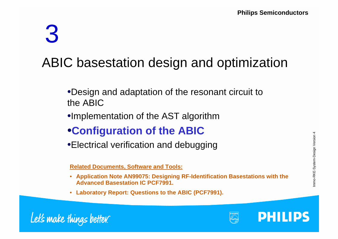
ABIC basestation design and optimization
•Design and adaptation of the resonantcircuit to the ABIC•Implementation of the AST algorithm•Configuration of the ABIC•Electrical verification and debugging
3
Related Documents, Software and Tools:
• Application Note AN99075: Designing RF-Identification Basestations with theAdvanced Basestation IC PCF7991.
• Laboratory Report: Proposal for a Circuit Design and PCB-Layout for the PCF7991(ABIC)
• User Manual and Tool: Transponder Evaluation and Development Kit (TED-Kit)HSIS/UM9907.

Imm
o-R
KE
-Sys
tem
-Des
ign
Ver
sion
4
Philips Semiconductors
Basic specifications for ABIC basedsystems
• ABIC:- maximum antenna current: Imax,p = 200 mAp (Burst mode: 400 mAp)- output voltage: Vout = 5V * 4/π= 6.3 Vp- maximum Rx-pin-input voltage: VRx,p = 7..8 Vp
• basestation inductance value range: L = 350 .. 1200 µH
• basestation quality factor range: Q = 5 .. 15

Imm
o-R
KE
-Sys
tem
-Des
ign
Ver
sion
4
Philips Semiconductors
ABICABIC
Basestation Design Example
Antenna
Ra
Ca
La
Tx1
Rx
Tx2
Rx
Ia = 200mAp
GND
Vout = 6.3VpQGND
VRX = 7..8Vp(Rint,max = 33k)
• Choose La = 400µH
• Ca = 1 / La / (2 pi fres)2 = 4nF
• Ra = Vout / Ia = 32 Ohms
• Q = 2 pi fres La / Ra => Q = 10 (in range)
• VRx = Vtap Rint,max / (Rx + Rint,max) => Rx
(Vtap = Q Vout = 63Vp)
• k = 1% (measured)
• Coil Design...
RWD

Imm
o-R
KE
-Sys
tem
-Des
ign
Ver
sion
4
Philips Semiconductors
Basestation Coil Design
Read/WriteDevice
Read/WriteDevice
L rr
dNA= ⋅ ⋅ ⋅ ⋅ ⋅
⋅4
2 1 85π πln ,
L inductance [nH]r antenna radius [cm]d wire diameter [cm]NA number of turns
Inductance value, calculated by this formula, is strongly influenced by metal and ferritein the vicinity of the coil.

Imm
o-R
KE
-Sys
tem
-Des
ign
Ver
sion
4
Philips Semiconductors
ABIC basestation design and optimization
•Design and adaptation of the resonant circuit tothe ABIC
•Implementation of the AST algorithm•Configuration of the ABIC•Electrical verification and debugging
3
Related Documents, Software and Tools:
• Application Note AN99075: Designing RF-Identification Basestations with theAdvanced Basestation IC PCF7991.
• User Manual and Software HSIS/UM9708: Control Software Library for PDF7991ATand PCF7936AS.

Imm
o-R
KE
-Sys
tem
-Des
ign
Ver
sion
4
Philips Semiconductors
Adaptive-Sampling-Time Principle
V1
R1
L1
phasedifference
ϕϕϕϕ φφφφs = 2∗ϕ − π/2 = 2∗ϕ − π/2 = 2∗ϕ − π/2 = 2∗ϕ − π/2
VC
low passfilter VDemod
phaseshifter and multiplier are realized as sample and hold detector
synchronous detector
• only one demodulator good price/performance ratio
• correct demodulation from the first bit on short authentication time
• demodulation of only one data stream required low µC calculationpower, low µC price

Imm
o-R
KE
-Sys
tem
-Des
ign
Ver
sion
4
Philips Semiconductors
AST Implementation
V1
phasedifference
VC
sampling resolution:
R1
L1
LP
360°64 = 5,625°
µC
φs = 2 φant + φoffs
ABIC
φφφφant
φφφφs
Data

Imm
o-R
KE
-Sys
tem
-Des
ign
Ver
sion
4
Philips Semiconductors
Microcontroller Function
void Ast_Adjust (UBYTE t_offset)
UBYTE t_antenna;
t_antenna = READ_PHASE();t_antenna <<= 1; // multiply by 2t_antenna += t_offset; // add compensation constantt_antenna &= 0x3F; // mask outSET_SAMPLING_TIME(t_antenna);
Imm
o-R
KE
-Sys
tem
-Des
ign
Ver
sion
4
Philips Semiconductors
ABIC basestation design and optimization
•Design and adaptation of the resonant circuit tothe ABIC•Implementation of the AST algorithm
•Configuration of the ABIC•Electrical verification and debugging
3
Related Documents, Software and Tools:
• Application Note AN99075: Designing RF-Identification Basestations with theAdvanced Basestation IC PCF7991.
• Laboratory Report: Questions to the ABIC (PCF7991).

Imm
o-R
KE
-Sys
tem
-Des
ign
Ver
sion
4
Philips Semiconductors
Extended block diagram of the ABIC
RX
EMI filter
TEST_SAMPLING_PHASE
Samplingdemodulator Amplifier 0 Amplifier 1
+-
DOUT
40/160Hz
32/16
32/6
3/6kHz
FIL
TE
RH
FIL
TE
RL
GA
IN0*
GA
IN1*
DIS
SM
AR
TC
OM
P
HY
ST
ER
ES
IS
Control Register
TEST_ANAOUT
TEST_3900Hz
TEST_OFFlowest internal clock
Inputprotection
MODE
ABIC
RIRX
QGND
Rv
Vtap
VIR
X
Control Register
TH
RE
SE
T
DIS
LP1
FR
EE
ZE
0/1
SmartComparator
Lowpassfilter
Highpassfilter
*gain values without filter attenuation

Imm
o-R
KE
-Sys
tem
-Des
ign
Ver
sion
4
Philips Semiconductors
Configuration of the ABIC
DISSMART-COMP
Contents of the Configuration Pages
• one config page contains 4 bit
• realized as RAM (not EEPROM)
GAIN1 GAIN0 FILTERH FILTERL
PD_MODE PD HYSTERESIS TXDIS
THRESET ACQAMP FREEZE1 FREEZE0
DISLP1 FSEL1 FSEL0
Page:
0
1
2
3
Bit 0 Bit 3

Imm
o-R
KE
-Sys
tem
-Des
ign
Ver
sion
4
Philips Semiconductors
Configuration of the ABICOptimum filter settings for HITAG2/STARC based systems
• The following filter settings are adapted to the spectral properties of the Manchester/CDP code with a datarate of 4 kBit/s
• Main low pass cutoff frequency: 6k Hz (FILTERL = 1)
• Main high pass cutoff frequency: 160 Hz (FILTERH = 1)
• Main low pass is enabled (DISLP1 = 0)
Optimization of the ABIC gain settings• we propose to choose the demodulator gain in order to have at least a voltage of 2Vpp demodulated
signal at the input of the smart comparator (check TEST_ANAOUT as explained in this training) for theweakest baseband signal expected in the given system
• 2 mVpp would correspond to the minimum receiver sensitivity multiplied by the maximum gain of the ABIC
• the weakest baseband signal occurs for the worst case combination of transponder resonant frequencytolerance and basestation resonant frequency tolerance

Imm
o-R
KE
-Sys
tem
-Des
ign
Ver
sion
4
Philips Semiconductors
ABIC basestation design and optimization
•Design and adaptation of the resonant circuit tothe ABIC•Implementation of the AST algorithm•Configuration of the ABIC
•Electrical verification and debugging
3
Related Documents, Software and Tools:
• Application Note AN99075: Designing RF-Identification Basestations with theAdvanced Basestation IC PCF7991.

Imm
o-R
KE
-Sys
tem
-Des
ign
Ver
sion
4
Philips Semiconductors
ABIC Block Diagram
Antenna Drivers
ControlUnit
Oscillator
Serial Interface
Control Register
SynchronDemodulator
PhaseMeasurement
Bandpass FilterAmplifier
Dynamic ControlDigitizer
TX1
TX2
RX
QGND CEXT VSS
XTAL1
XTAL2
DIN
DOUT
SCLK
VDD
MODE
Modulator
to µC
VDD
100 nF
100 nF 100 nF
10 µF
1
2
VDD
1 M 1 nF3
4
Rx

Imm
o-R
KE
-Sys
tem
-Des
ign
Ver
sion
4
Philips Semiconductors
System verification
•Tolerance field verification by simulation•Tolerance field verification by measurement•Temperature, humidity and functional tests•EMC measurements and optimization
4
Related Documents, Software and Tools:
• Application Note AN99075: Designing RF-Identification Basestations with theAdvanced Basestation IC PCF7991.

Imm
o-R
KE
-Sys
tem
-Des
ign
Ver
sion
4
Philips Semiconductors
Tolerance Field Diagrams
• Verification method during and after design phase• Due to production and temperature tolerances, the resonant frequencies of
transponder and basestation antenna are changed• In practice, nearly all combinations of transponder and basestation
resonant frequencies are possible• Tolerance field shows the safe operating area of the system in means of
transponder and basestation tolerance• Tolerance fields can be determined in two ways
− by simulation− by measurements

Imm
o-R
KE
-Sys
tem
-Des
ign
Ver
sion
4
Philips Semiconductors
Philips Tolerance Field Simulation Program
There are two different tolerance fields calculated, as function of theresonant frequency of two inductively coupled resonant circuits:
• the energy transfer function
• the amplitude of the demodulated data received from the transponder
The following restrictions apply:
• Calculation is done in the Frequency domain; transients in time domainare neglected
• the calculation is restricted to the fundamental; higher harmonics areneglected
• modelling the transponder by pure ohmic load (power dissipation andload modulation)
• V/I transfer function of the transponder is linearized (pice-wise)
• modelling the demodulator of the basestation by math. model

Imm
o-R
KE
-Sys
tem
-Des
ign
Ver
sion
4
Philips Semiconductors
Simulation Capabilities
Important Note:
• Due to the given restrictions, the simulations can not replace practicalmeasurements and qualification of the transponder system
• Measurements, which include temperature effects, aging and otherparameter of the used devices, have to be done in addition to the followingsimulations
Following, one option to do worst case simulations with the PHILIPSsimulation tool ‚TOLSIMU‘ is shown on an example with practical values.

Imm
o-R
KE
-Sys
tem
-Des
ign
Ver
sion
4
Philips Semiconductors
Example (1): Given Parameters
System:
• k = 1.8% (min)
Base station: PCF7991AT (ABIC) :
• VDD = 4.9V - 5.1V (5V +- 2%)
• ROTX = 0 - 7 Ohm (Driver resistance ABIC in full bridge)
Base station antenna:
• L = 601µH - 651µH
• RReihe = 29.1 - 29.7 Ohm
• RCU,FE = 22 - 24.4 Ohm

Imm
o-R
KE
-Sys
tem
-Des
ign
Ver
sion
4
Philips Semiconductors
Example (2): Derived Parameters
Base station antenna quality factor:
• Q1 = ( 2* PI * 125e3 * L ) / ( RReihe + ROTX + RCU,FE )
• Q1min = ( 2* PI * 125e3 * 601e-6 ) / ( 29.7 + 7 + 24,4 )
• Q1min = 7.72
• Q1max = ( 2* PI * 125e3 * 651e-6 ) / ( 29.1 + 0 + 22 )
• Q1max = 10
External Resistor at Rx:
• RV,MIN = RIRX,MAX * ( (VDD,MAX *4/PI * Q1max ) / VIRX,MAX - 1 )
• RV,MIN = 235 kOhm
• RV,NOM = 270 kOhm (choosen according to IEC-E24, 2% Toleranz)

Imm
o-R
KE
-Sys
tem
-Des
ign
Ver
sion
4
Philips Semiconductors
Example (3): Derived Parameters
Minimal amplitude of the modulated voltage at base station antenna:
• VRX = 3 mV (peak) (ABIC gain at 1000)
• VMOD = ( RV,MAX / RIRX,MIN + 1 )* VRX
• VMOD = 51.6 mV (peak)

Imm
o-R
KE
-Sys
tem
-Des
ign
Ver
sion
4
Philips Semiconductors
Example (4): Simulation 1, Demodulation of TXP data
Used simulation parameters:
• k = 1.8%
• fOSC = 125kHz (+-0.3% => two plots in one diagram)
• VDD = 4.9V
• L = 651
• Q1 = 7.72
• VMOD = 51.6 mV (display the 52mV line at tap point)
• Standard HITAG2 Transponder Model

Imm
o-R
KE
-Sys
tem
-Des
ign
Ver
sion
4
Philips Semiconductors
Example (5): Simulation 1, Demodulation of TXP data
52
52
L1=0.651mH, Q1=7.7, Q2=35.0, k=1.80%, U1=6.24V , I1max= 94mA
-3.2%
3.2%
7.7% 18.3
52
52

Imm
o-R
KE
-Sys
tem
-Des
ign
Ver
sion
4
Philips Semiconductors
Example (6): Simulation 2, Energy transfer
Used simulation parameters:
• k = 1.8%
• VDD = 4.9V
• L = 651µH
• Q1 = 7,72
• Energy: Standard HITAG2-Model

Imm
o-R
KE
-Sys
tem
-Des
ign
Ver
sion
4
Philips Semiconductors
Example (7): Simulation 2, Energy transfer
4
4
L1=0.651mH, Q1=7.7, Q2=35.0, k=1.80%, U1=6.24V , I1max= 94mA
-3.2%
3.2%
26.5%

Imm
o-R
KE
-Sys
tem
-Des
ign
Ver
sion
4
Philips Semiconductors
System verification
•Tolerance field verification by simulation
•Tolerance field verification by measurement•Temperature, humidity and functional tests•EMC measurements and optimization
4
Related Documents, Software and Tools:
• Application Note AN99075: Designing RF-Identification Basestations with theAdvanced Basestation IC PCF7991.

Imm
o-R
KE
-Sys
tem
-Des
ign
Ver
sion
4
Philips Semiconductors
Tolerance Field Measurement Setup (Principle)
LaCa0
Rv
TX1
TX2
RX
Ra
Ca1
Ca2
Can
...
Ct1
Ct2
Ctm.. .
Ct0
Lt
Transponder(bondout version)

Imm
o-R
KE
-Sys
tem
-Des
ign
Ver
sion
4
Philips Semiconductors
System verification
•Tolerance field verification by simulation•Tolerance field verification by measurement
•Temperature, humidity and functional tests•EMC measurements and optimization
4
Related Documents, Software and Tools:
• Important information about relevant tests and test conditions can be found in the‘Product Qualification Packages’ of the particular products.

Imm
o-R
KE
-Sys
tem
-Des
ign
Ver
sion
4
Philips Semiconductors
Temperature, humidity and functional tests• Temperature and humidity chamber tests should be done according to the maximum operating
conditions given in the module specification
• Temperature and humidity chamber tests should be done with ALL transponder system componentsincluded (basestation electronics, immobilizer coil and transponder)
• Functional tests should be done with a larger number of devices to get statistically relevant results
• The ICs used in the tested modules should be taken from different batches

Imm
o-R
KE
-Sys
tem
-Des
ign
Ver
sion
4
Philips Semiconductors
System verification
•Tolerance field verification by simulation•Tolerance field verification by measurement•Temperature, humidity and functional tests
•EMC measurements and optimization
4
Related Documents, Software and Tools:
• Application Note AN99075: Designing RF-Identification Basestations with theAdvanced Basestation IC PCF7991.
• Laboratory Report: Questions to the ABIC (PCF7991).

Imm
o-R
KE
-Sys
tem
-Des
ign
Ver
sion
4
Philips Semiconductors
ABIC-EMC guidelines (1)
Antenna Drivers
ControlUnit
Oscillator
Serial Interface
Control Register
SynchronDemodulator
PhaseMeasurement
Bandpass FilterAmplifier
Dynamic ControlDigitizer
TX1
TX2
RX
QGND CEXT VSS
XTAL1
XTAL2
DOUT
DIN
SCLK
VDD
MODE
Modulator
to µC
VDD
100 nF
100 nF 100 nF
10 µF
Rv
Digital GlitchFilter
ProgrammableClock Divider
EMI Filter

Imm
o-R
KE
-Sys
tem
-Des
ign
Ver
sion
4
Philips Semiconductors
ABIC-EMC guidelines (2)• It is extraordinary important to place Rv as close as possible to the RX-pin for optimum EMI-
performance.
• The power supply shall be bypassed (de-coupled) via a 10µF or larger capacitor in parallel to a 100nFcapacitor
• For bypassing the internal analog virtual ground (~2V), a 100nF capacitor has to be connected from theQGND-pin to the VSS-pin. This capacitor connection should be low impedance and close to the IC.
• Another 100nF capacitor is connected from CEXT to VSS, which is needed for the 2nd high pass filter.This capacitor connection should be low impedance and close to the IC too.
• It is recommended to place a guard ring at the QGND potential around the CEXT-pin - capacitor lead, toprevent leakage currents into CEXT.
• The usage of the internal ABIC glitch filters should be considered depending on the particularapplication.

Imm
o-R
KE
-Sys
tem
-Des
ign
Ver
sion
4
Philips Semiconductors
ABIC-EMC guidelines (3)• The value of the pull-up resistors of the serial interface (DIN, DOUT, SCLK) should be chosen to
minimize the influence of external disturbers on these lines. This can be verified during measurementsof these signals under EMC conditions.
• Increasing the Q-factor of the basestation antenna to improve the selectivity of the basestation resonantcircuit.
Please read the relating chapters of the ABIC application note very carefully,which provide additional hints and background information concerning thepresented topics.

Imm
o-R
KE
-Sys
tem
-Des
ign
Ver
sion
4
Philips Semiconductors
Hints for EM-Susceptibility measurements (1)Separate measurements at the ABIC-MODE-pin in TEST_ANAOUT -modeunder the following conditions:
• A) the demodulated signal amplitude (without disturber, only transponder modulation)
• B) the ‘demodulated’ noise amplitude (only disturber active to measure susceptibility)
• By doing these measurements the signal to noise ratio (depending on the disturber carrierfrequency) of the system can be
Doing measurements on the system with an oscilloscope using the post-trigger mode:
• In case of a communication error during EMC-measurements, a post-trigger is generated bythe basestation application software
• The other channels of the oscilloscope are connected to important signals like RX, DIN,DOUT, SCLK and VDD
• By this, the prehistory of the error can be observed and countermeasures can be done
• Note: Measurements during EMC tests may have strong influence on the systemperformance and EMC behaviour, due to the susceptibility of the measurement probes andcables.

Imm
o-R
KE
-Sys
tem
-Des
ign
Ver
sion
4
Philips Semiconductors
Hints for EM-Susceptibility measurements (2)Doing measurements on the system with reduced disturber field strength:
• Susceptibility can be measured with e.g. Ereduced = 50V/m instead of Enominal = 100V/m (valuesdepend on the used EMC specification)
• This can be done, to find the most critical disturber frequencies. Note: Provided that afterEMC-measurements only go/no-go information is available (measurement with fixed disturberfield strength).
• This information can then be used for example to design optimised adapted filters.
Imm
o-R
KE
-Sys
tem
-Des
ign
Ver
sion
4
Philips Semiconductors
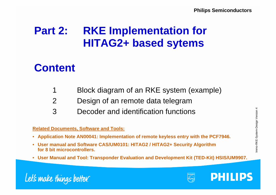
Part 2: RKE Implementation forHITAG2+ based sytems
Content
1 Block diagram of an RKE system (example)2 Design of an remote data telegram3 Decoder and identification functions
Related Documents, Software and Tools:
• Application Note AN00041: Implementation of remote keyless entry with the PCF7946.
• User manual and Software CAS/UM0101: HITAG2 / HITAG2+ Security Algorithmfor 8 bit microcontrollers.
• User Manual and Tool: Transponder Evaluation and Development Kit (TED-Kit) HSIS/UM9907.

Imm
o-R
KE
-Sys
tem
-Des
ign
Ver
sion
4
Philips Semiconductors
Block diagram of an RKE system (example)m`cTVQS
HrecJ
qê~åëãáííÉê
recJoÉÅÉáîÉê
Modulated data-stream (UHF)
jáÅêçÅçåíêçääÉê
aÉÅçÇÉêJ=~åÇ=fÇÉåíáÑáÅ~íáçåÑìåÅíáçåë
_ìë=áåíÉêÑ~ÅÉ
Demodulated data-stream (Baseband)
_~ëÉëí~íáçå=ãÉãçêóEbbmoljLo^jF
IDE1…IDEn(1)
SI1…SIn(1)
SYNC1…SYNCn(1)
_çÇó=ÅçãéìíÉê
(1) These values must be stored in the basestation memory for each car remote control (1..n) separately
Basestation
Remote control unit / FOB
Serial car bus

Imm
o-R
KE
-Sys
tem
-Des
ign
Ver
sion
4
Philips Semiconductors
Design of an remote data telegram (1)Typical system requirements
• íÜÉ=ã~ñáãìã=êÉÅÉáîÉê=ï~âÉ=ìé=íáãÉ=áåÅäìÇáåÖ=íÜÉ=éçääáåÖ=ÅóÅäÉ=çÑ=íÜÉ=recJêÉÅÉáîÉê Ñçê=~=íóéáÅ~ä=ëÉäÑ=éçääáåÖ=ëóëíÉã=í
ob`j^u=Y=OR=ãë
• íÜÉ=ëóëíÉã=êÉëéçåëÉ=íáãÉ=íç=~=Äìííçå=éêÉëëáåÖ=íobp=
Y=NMM=ãë
• ÇÉã~åÇ=çÑ=êÉÇìåÇ~åÅó=çÑ=íê~åëãáííÉÇ=Ç~í~=ÄäçÅâë=íç=ÖÉí=ãçêÉ=ëóëíÉã=íçäÉê~åÅÉ=áåÅ~ëÉ=çÑ=íê~åëãáëëáçå=Éêêçêë=çê=ÉñíÉêå~ä=ÇáëíìêÄ~åÅÉë
• äçï=éçïÉê=Åçåëìãéíáçå=çÑ=íÜÉ=Ä~ííÉêó=éçïÉêÉÇ=êÉãçíÉ=Åçåíêçä=ìåáí
• ëéÉÅáÑáÅ~íáçå=çÑ=íÜÉ=iba=Ääáåâ=ÑêÉèìÉåÅó=~åÇ=áíë=Çìíó=ÅóÅäÉ
• Ñ~ëí=~åÇ=ë~îÉ=ÇÉíÉÅíáçå=çÑ=Äìííçå=êÉäÉ~ëÉ=EÉKÖK=Ñçê=ÅçãÑçêí=ÑìåÅíáçåë=äáâÉ=ÚçéÉå=Å~ê=ïáåÇçïëÛF
• éêÉîÉåíáçå=çÑ=ÇáëÅÜ~êÖáåÖ=íÜÉ=Ä~ííÉêó=ÇìÉ=íç=ìåáåíÉåíáçå~ä=Äìííçå=éêÉëëáåÖ
• ëéÉÅáÑáÅ~íáçå=çÑ=~=é~êíáÅìä~ê=íê~åëãáííÉê=ÅáêÅìáí

Imm
o-R
KE
-Sys
tem
-Des
ign
Ver
sion
4
Philips Semiconductors
Design of an remote data telegram (2)Hitag2+ data telegram format
Run-In Key IdentifierSequence
IncrementCommand
SequenceResponse P
arity
26 bit 32 bit 4 bit 10 bit 32 bit 8 bit
114 bit/Block (inc. 2 filling bits)
tdata
t init
Data Frame 1 Data Frame 2 Data Frame n
Transmit
Cycle Time t cycle
Transmit
ttrans
ttrans
1 2 RDHT
Rolling Code Block (RCB)

Imm
o-R
KE
-Sys
tem
-Des
ign
Ver
sion
4
Philips Semiconductors
Design of an remote data telegram (3)Example for a typical remote data telegram
8 x WUP 3 x RCB 8 x LED 30 x SIB 2 x LED 30 x SIB 2 x LED 1 x BRB
TWUP TON-RC TON-SI
TSI-CYCLE
TSIF
3 x TRCB TRCB
26.6 ms 71.25 ms 190 ms 47.5 ms
760 ms
23.75 ms
25 s

Imm
o-R
KE
-Sys
tem
-Des
ign
Ver
sion
4
Philips Semiconductors
Decoder and identification functions (1)
Synchronise to RUN-IN
Receiver / µC wake up
Read and decode remotetelegram
RCB/SIB/BitcountError?
SIFOB,LOW =SIBAS,LOW ?
SIB
yes (SIB valid)
M
No(wrong SIB)
M
N
RCB/BRB
wrong Bitcount
RUN-IN synchronization andManchester decoder
M
Timeout detected(285 ms or 95 ms)
Init_timeout = 95 ms
M
Button release notification
M
See FlowchartPart 2

Imm
o-R
KE
-Sys
tem
-Des
ign
Ver
sion
4
Philips Semiconductors
Decoder and identification functions (2)
IDE valid ? M
no
SIFOB.LOW incapture range?(2)
no
yes (RCB)
Calculate the sequence response of the basestation:SRBAS=f(IDEFOB,RSKBAS,CIDFOB,SI
HIGH,BAS(IDE)(5)
+SI LOW,FOB)
yes
SRBAS = SRFOB ?no
Resynchronisation: SILOW,BAS(IDE)= SILOW,FOB
yes
M
wrongParity ?(1)
right
N
SIFOB.LOW inself synch. capture range? (3)
no
Calculate the sequence response of the basestation:SRBAS=f(IDEFOB,RSKBAS,CIDFOB,SYNCHIGH,BAS(IDE)
+SI LOW,FOB)
yes
SRBAS = SRFOB ?M
no
Resynchronisation: SILOW,BAS(IDE)= SILOW,FOB
yes
M
+8000200h(4)
M
SIHIGH,BAS(IDE)=SYNCHIGH,BAS+8000200h(4)SIHIGH,BAS(IDE)= SIHIGH,BAS(IDE) + 1024d(5)
Button pressing notification
Init_timeout = 285 ms
CID != 0?
right
Button releasenotification
M
no (BRB)

Imm
o-R
KE
-Sys
tem
-Des
ign
Ver
sion
4
Philips Semiconductors
Appendix1: Overview about documents, software and tools,referenced in this presentation
Part1: Immobilizer Design
• Application Note AN99075: Designing RF-Identification Basestations with the AdvancedBasestation IC PCF7991.
• User Manual and Software HSIS/UM9708: Control Software Library for PDF7991ATand PCF7936AS.
• User Manual and Tool: Transponder Evaluation and Development Kit (TED-Kit)HSIS/UM9907.
• Laboratory Report: Questions to the ABIC (PCF7991).
• Laboratory Report: Proposal for a Circuit Design and PCB-Layout for the PCF7991(ABIC).
• ‘Product Qualification Packages’ of the particular products.

Imm
o-R
KE
-Sys
tem
-Des
ign
Ver
sion
4
Philips Semiconductors
Appendix2: Overview about documents, software and tools,referenced in this presentation
Part2: RKE Design
• Application Note AN00041: Implementation of remote keyless entry with the PCF7946.
• User manual and Software CAS/UM0101: HITAG2 / HITAG2+ Security Algorithmfor 8 bit microcontrollers.
• User Manual and Tool: Transponder Evaluation and Development Kit (TED-Kit)HSIS/UM9907.

Imm
o-R
KE
-Sys
tem
-Des
ign
Ver
sion
4
Philips Semiconductors
Appendix3: Revision History
• Version 1 First Version
• Version 2 References to related documents, software and tools are given at thebeginning of every chapter.
• Version 3 Chapter about the HITAG2+ RKE implementation added.
• Version 4 Chapter about worst case tolerance field simulations added.