Imaging Coherent Electron Flow Through Semiconductor ... · iii Abstract Imaging Coherent Electron...
210
Imaging Coherent Electron Flow Through Semiconductor Nanostructures A thesis presented by Brian James LeRoy to The Department of Physics in partial fulfillment of the requirements for the degree of Doctor of Philosophy in the subject of Physics Harvard University Cambridge, Massachusetts May, 2003
Transcript of Imaging Coherent Electron Flow Through Semiconductor ... · iii Abstract Imaging Coherent Electron...

Imaging Coherent Electron Flow Through
Semiconductor Nanostructures
A thesis presented
by
Brian James LeRoy
to
The Department of Physics
in partial fulfillment of the requirements
for the degree of
Doctor of Philosophy
in the subject of
Physics
Harvard University
Cambridge, Massachusetts
May, 2003

© 2003 by Brian James LeRoy
All rights reserved.

iii
Abstract
Imaging Coherent Electron Flow Through Semiconductor Nanostructures
Advisor: Robert Westervelt Author: Brian LeRoy
Scanning probe microscopy is used to probe coherent electron flow in
semiconductor nanostructures. We have developed a technique for imaging coherent
electron flow through a two-dimensional electron gas (2DEG). The images are acquired
using a scanning probe microscope at low temperature. The conductance through the
device as a function of tip position is measured to obtain an image of electron flow. The
images of electron flow are decorated by interference fringes spaced by half the Fermi
wavelength. We use the spacing of these fringes to measure the local electron density.
The variation of the density with back gate voltage agrees with a parallel plate capacitor
model.
We use our imaging technique to characterize the rate of energy loss for electrons
traveling through the 2DEG. A source-drain voltage is applied to the electrons, which
accelerates them and causes them to loss energy more quickly. By imaging the electron
flow, the rate that the electrons lose their excess energy is determined. The results agree
with the electron-electron scattering rate in a 2DEG for different distances and energies.
Images of electron flow through three electron-optic devices are presented. An
electrostatic prism is used to control the direction of electron flow based on the density
under its gate. Images are shown using a round gate as a defocusing lens for electron

iv
waves and as a circular scatterer. The potential profile from an electrostatic gate is
investigated by creating a narrow channel for electrons. By imaging the trajectories of
electrons, the profile of the potential from the gate is found.
The origin of the interference fringes, which decorate all of our images of electron
flow is investigated. They are due to interference between paths backscattered from the
tip and ones backscattered from scattering objects at nearly the same distance. This is
confirmed by the addition of a small reflecting gate, which enhances the interference
fringes at the same distance from the quantum point contact. The interference fringes
move as the position of the reflector is changed indicating that the fringes are due to
backscattering from the reflector.
v
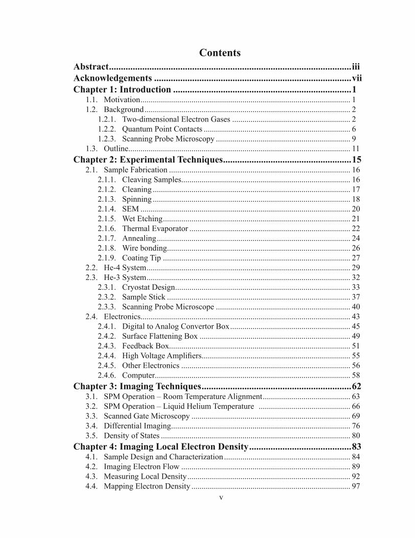
ContentsAbstract......................................................................................................iiiAcknowledgements ...................................................................................viiChapter 1: Introduction ...........................................................................1
1.1. Motivation....................................................................................................... 11.2. Background ..................................................................................................... 2
1.2.1. Two-dimensional Electron Gases .......................................................... 21.2.2. Quantum Point Contacts ........................................................................ 61.2.3. Scanning Probe Microscopy .................................................................. 9
1.3. Outline............................................................................................................. 11Chapter 2: Experimental Techniques......................................................15
2.1. Sample Fabrication ......................................................................................... 162.1.1. Cleaving Samples................................................................................... 162.1.2. Cleaning ................................................................................................. 172.1.3. Spinning ................................................................................................. 182.1.4. SEM ....................................................................................................... 202.1.5. Wet Etching............................................................................................ 212.1.6. Thermal Evaporator ............................................................................... 222.1.7. Annealing............................................................................................... 242.1.8. Wire bonding.......................................................................................... 262.1.9. Coating Tip ............................................................................................ 27
2.2. He-4 System.................................................................................................... 292.3. He-3 System.................................................................................................... 32
2.3.1. Cryostat Design...................................................................................... 332.3.2. Sample Stick .......................................................................................... 372.3.3. Scanning Probe Microscope .................................................................. 40
2.4. Electronics....................................................................................................... 432.4.1. Digital to Analog Convertor Box........................................................... 452.4.2. Surface Flattening Box .......................................................................... 492.4.3. Feedback Box......................................................................................... 512.4.4. High Voltage Amplifiers......................................................................... 552.4.5. Other Electronics ................................................................................... 562.4.6. Computer................................................................................................ 58
Chapter 3: Imaging Techniques...............................................................623.1. SPM Operation – Room Temperature Alignment........................................... 633.2. SPM Operation – Liquid Helium Temperature ............................................. 663.3. Scanned Gate Microscopy .............................................................................. 693.4. Differential Imaging........................................................................................ 763.5. Density of States ............................................................................................. 80
Chapter 4: Imaging Local Electron Density...........................................834.1. Sample Design and Characterization .............................................................. 844.2. Imaging Electron Flow ................................................................................... 894.3. Measuring Local Density................................................................................ 924.4. Mapping Electron Density .............................................................................. 97

vi
Chapter 5: Imaging Electron Energy Loss .............................................1015.1. Measurement Technique ................................................................................. 1025.2. Images of Electron Flow................................................................................. 1045.3. Theoretical Scattering Rate............................................................................. 111
Chapter 6: Electron Optics ......................................................................1166.1. Electrostatic Prism .......................................................................................... 1176.2. Circular Scatterer ............................................................................................ 1226.3. Narrow Channel .............................................................................................. 129
Chapter 7: Imaging Interference Fringes...............................................1367.1. Origin of Fringes............................................................................................. 1377.2. Fringe movement ............................................................................................ 1467.3. Temperature Dependence................................................................................ 152
Chapter 8: Conclusions and Future Directions......................................157References ..................................................................................................161Appendix A. SEM Procedure...................................................................166
A.1. Loading Sample ............................................................................................. 166A.2. Initial Images .................................................................................................. 166A.3. Aligning and Focusing ................................................................................... 167A.4. Writing ........................................................................................................... 167A.5. JEOL Control ................................................................................................. 168A.6. Shut Down ..................................................................................................... 168
Appendix B. Script Commands ...............................................................169B.1. Utility Commands........................................................................................... 169B.2. Graphics Commands....................................................................................... 174B.3. Scan Commands.............................................................................................. 179B.4. Sweep Manipulation Commands .................................................................... 185B.5. Printing Commands ........................................................................................ 190B.6. Movie Commands........................................................................................... 191B.7. Loop and Variable Commands........................................................................ 194B.8. Setup Commands ............................................................................................ 195B.9. Data Taking Commands.................................................................................. 197B.10. Simulation Commands.................................................................................... 198B.11. MetaScan Commands ..................................................................................... 199B.12. Autoalign Commands ..................................................................................... 200B.13. Powerscan Commands .................................................................................... 201
vii
Acknowledgements
During the last five years, I have had the pleasure of working with many people
here at Harvard who have made my graduate school experience very enjoyable. First of
all, I want to thank my adviser, Bob Westervelt, for having an excellent lab in which to
do research. He has created an environment where everyone is free to explore their own
research projects yet is always willing to give suggestions and advice.
I also want to thank the other two members of my committee. Rick Heller and his
group have always been available to talk to about results from our imaging experiments.
They have also been very helpful in running quantum mechanical simulations of the
electron flow to better understand the results. The addition of Charlie Marcus and his
group has added another group of people to the second floor of McKay who are interested
and knowledgeable in 2DEGs. This has provided a welcome group to discuss the
experiments that I have worked on.
In our group, I have worked with several people on the imaging project. Mark
Topinka and I struggled for nearly a year to get the AFM to work and take the first images
of electron flow. Over the last few years, I have enjoyed teaching Ania Bleszynski and
Kathy Aidala how to use the AFM and working with them to set up our group’s new He-3
AFM. I look forward to seeing the results of their experiments at lower temperatures and
with new materials. During my time in the group, I have had the pleasure of working
with many other people. Ian Chan joined the lab the same year as I did and has helped to
keep all of the computers running smoothly and is always around to answer electronics
questions. Thanks to Hakho Lee for our seemingly daily cups of coffee after the lab

viii
got an espresso machine, the extra caffeine made the thesis writing process go more
quickly. I also want to thank Lester Chen, Marija Drndic, Dave Duncan, Parisa Fallahi,
David Goldhaber-Gordon, Chungsok Lee, and Andy Vidan who have been around the
Westervelt lab during the same time as me. You guys have always been available and
willing to discuss and provide ideas for my experiments.
In order to perform the experiments described in this thesis many different pieces
of equipment are necessary. There are many people who work hard so that we can do our
experiments without having to constantly fix things. I want to thank Steve Shepard for
his work in keeping everything running smoothly in the cleanroom especially with the
addition of the basement cleanroom and all of the new equipment. Also, thanks to Yuan
Lu for his work with the SEMs including changing the JEOL’s filament on very short
notice.
Thanks to my family for supporting me throughout all my years in school. I want
to thank Bess for always being there for me, even when we were far apart during my first
two years at Harvard. I am looking forward to many more exciting times as we move on
with our lives.
1
Chapter 1
Introduction
1.1. Motivation
For more than 15 years, the growth of high mobility two-dimensional electron
gases has allowed many new experiments in the field of mesoscopic physics. These
experiments have demonstrated new and unexpected phenomena including conductance
quantization, the integer and fractional quantum Hall effect, and single electron tunneling
[Beenakker, (1991); Sohn, (1997)]. However, most of these experiments relied on
transport measurements to understand these phenomena. The use of scanning probe
microscopy techniques allows the behavior of the electrons to be imaged on a much
smaller length scale then is accessible with standard transport measurements.
Scanning probe microscopy provides a novel way of examining electronics
devices even as they continued to be miniaturized. This is because they provide
information about the local behavior of the electrons rather than an average measure
over a macroscopic area. Our imaging techniques are also important for the design and
implementation of new devices that rely on the coherence of the electron, for example
quantum information processing devices, to perform computation. From our images
we are able to determine whether the flow is coherent and to image the pattern of flow
through a device. In this thesis, we examine the operation of some of these new types of
devices, including their pattern of electron flow and their scattering rate.
The design of new electronic materials requires methods to investigate their
2
properties. We show how scanning probe microscopy can be used to investigate the
local properties of these new materials. From our images of electron flow we are able to
spatially profile the local electron density. The images of electron flow are also decorated
by a new type of interference, which can be used in the creation of devices that rely on
the coherence of the electron for their operation.
1.2. Background
The advances in mesoscopic semiconductor devices have been driven by
improvements in material quality and fabrication techniques. Most notably, the
mobility of GaAs/AlGaAs heterostructures continues to increase and has now reached
3x107 cm2/V s [Pfeiffer, (1989)]. This increase has been caused by the development of
modulation doping techniques [Dingle, (1978)] and improved sample quality. The size
of devices that can be fabricated continues to decrease with improvements in electron
beam lithography. It is now possible to fabricate devices containing only a few electrons
[Tarucha, (1996); Ciorga, (2000); Elzerman, (2003)].
1.2.1. Two-dimensional Electron Gases
The samples that we use in all of the experiments described in this thesis contain
two-dimensional electron gases in GaAs/AlGaAs heterostructures. The heterostructures
are grown by molecular beam epitaxy, which ensures that the thickness of each layer
can be controlled with sub-monolayer precision [Herman, (1989)]. This control of the
growth properties allows arbitrary potential wells for electrons to be created. Some of
the basic shapes that can be made are square wells, triangular wells, parabolic wells and

3
superlattices.
For all of the experiments in this thesis we have used samples with accumulation
layers formed at the interface of GaAs and Al0.3
Ga0.7
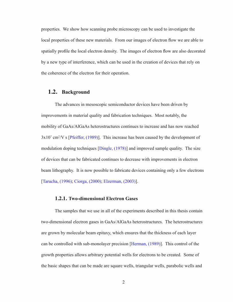
As. Figure 1.1 shows the
conduction band edge for a 2DEG sample. The 2DEG is formed between the GaAs
and AlGaAs layers due to the offset in the conduction band for these two materials.
This offset is determined by the difference in the bandgap and electron affinity for
Figure 1.1 Schematic band diagram showing the conduction band edge for the samples used in this thesis. The bottom portion shows the growth layers for the heterostructure.
4
GaAs and Al0.3
Ga0.7
As. This gives an offset in the conduction band of about 230 meV
[Adachi, (1985)]. The second consideration in finding the conduction band profile for
the heterostructure is that the Fermi level is pinned about 600 meV below the conduction
band edge due to the surface states [Davies, (1998)]. These states are compensated with
the delta layer of Si donor atoms, which give up electrons to satisfy the surface states
and create the 2DEG. The Si donor atoms fix the Fermi level about 120 meV below
the conduction band edge at their position [Davies, (1998)]. The last step to find the
conduction band profile is to calculate the slopes between these fixed points knowing the
distance and electron density.
The slope of the conduction band edge is calculated using a simple parallel
plate capacitor model. The distance and potential difference from the surface to the
Si donor atoms is known. Using this information, the number of electrons needed to
satisfy the surface states can be calculated. This leaves the rest of the Si atoms to give
their electrons to the 2DEG. The electrostatic attraction between the electrons in the
2DEG and the donor atoms creates an approximately triangularly shaped potential at
the interface of the GaAs and Al0.3
Ga0.7
As. The density of the Si donor atoms is chosen
so that only the lowest subband of the potential well is occupied. The energy levels of
this potential profile are well known and the wavefunction is given by an Airy function
[Harris, (1989)]. The equation for the energy eigenvalues of the well is
where F = 4πn/ε is the electric field due to the ionized donors, n is the electron density in
the 2DEG, ε is the dielectric constant of GaAs and m is the electron effective mass, which
€
Ei = h2
2m
1 3
3π2
i + 34
F
2 3
5
is 0.067 times the free electron mass. This provides the confinement in the z-direction
while the electrons are free in the x and y direction creating the 2DEG.
The Fermi energy of the 2DEG can be estimated from Figure 1.1 by fixing the
chemical potential throughout the sample. This gives the following equation for the
Fermi Energy.
where φdonor
≈ 120 mV, φoffset
≈ 230 mV and d is the distance from donors to the 2DEG.
The model also can give the density of Si dopants needed to satisfy the surface states:
where r is the distance from the dopants to the surface, φsurface
≈ 600 mV, and η ≈ 1/2 is
the fraction of dopant atoms that are thermally activated, i.e. not all Si donors are active.
In the case of our heterostructure more of the electrons from the ionized donors go to the
surface states than go to the 2DEG.
Since the heterostructure is grown on a GaAs [100] surface, the Fermi surface for
electrons is just a circle. This gives a very simple dispersion relation between the Fermi
energy, EF, and the electron wavevector, k. This relation is given by
There is also a simple relationship between the wavevector, k, and the electron density, n,
since the electrons are confined to two dimensions.
The combination of these two equations shows that the Fermi energy is linear in the
electron density.
€
EF + eφdonor + Fd− eφoffset = E0
€
σ =e φsurface + φoffset − φdonor( )ε
4πrη
€
EF =h2(kx
2 +ky2 )
2m
€
n = k2
2π
6
1.2.2. Quantum Point Contacts
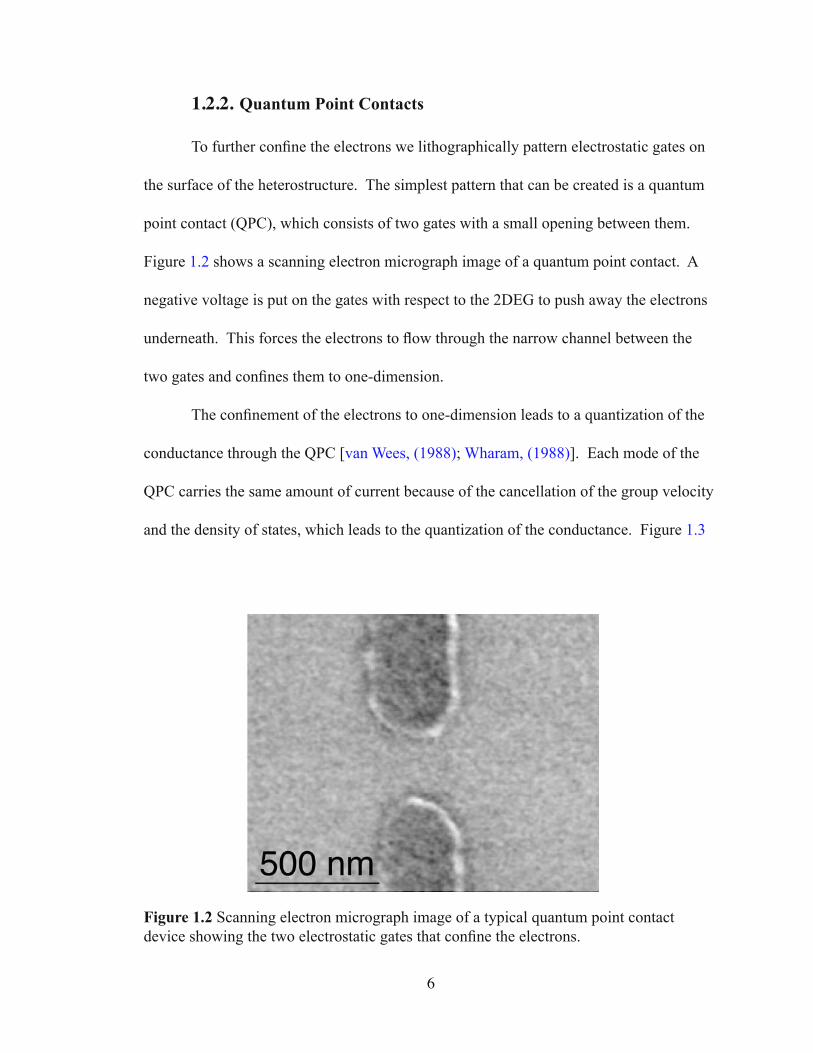
To further confine the electrons we lithographically pattern electrostatic gates on
the surface of the heterostructure. The simplest pattern that can be created is a quantum
point contact (QPC), which consists of two gates with a small opening between them.
Figure 1.2 shows a scanning electron micrograph image of a quantum point contact. A
negative voltage is put on the gates with respect to the 2DEG to push away the electrons
underneath. This forces the electrons to flow through the narrow channel between the
two gates and confines them to one-dimension.
The confinement of the electrons to one-dimension leads to a quantization of the
conductance through the QPC [van Wees, (1988); Wharam, (1988)]. Each mode of the
QPC carries the same amount of current because of the cancellation of the group velocity
and the density of states, which leads to the quantization of the conductance. Figure 1.3
Figure 1.2 Scanning electron micrograph image of a typical quantum point contact device showing the two electrostatic gates that confine the electrons.

7
shows the measured conductance through the QPC as a function of the voltage on its
gate at a temperature of 1.7 K. As the voltage is made more negative, the width of the
channel is decreased and transmission through the modes of the QPC is reduced. The
conductance of the QPC can be calculated using Landauer-Buttiker formalism if the
transmission probabilities of each mode are known [Landauer, (1957); Landauer, (1970);
Büttiker, (1986)]. The conductance, G, is given by the following equation
where the summation is over all of the modes of the QPC and the Ti are the transmission
probabilities of the individual modes through the QPC. If there is no scattering in the
QPC, the transmission probability is either 0 or 1 for each of the modes. This shows the
conductance quantized in units of 2e2/h depending on the number of modes accessible in
the QPC.
Figure 1.3 Conductance through a quantum point contact as a function of the voltage on its gate, which controls its width at a temperature of 1.7 K. The conductance shows well-defined plateaus at multiples of 2e2/h.
€
G = 2e2
hTi
i∑

8
When the electrons are confined to one-dimensional subbands the equation for
their energy versus wavevector has to be modified to account for the confinement. The
new equation is
where EN is the energy of the subband at the saddle point in the center of the QPC. It is
now clear that the electrons are only free in one dimension and their energy is quantized
in the other two directions. The energy of the one-dimensional subbands in the QPC
can be found by measuring the conductance as a function of the gate voltage and the
source-drain bias Vsd
. As the bias is increased the electrons are able to transverse the
QPC through higher subbands [Kouwenhoven, (1989)].
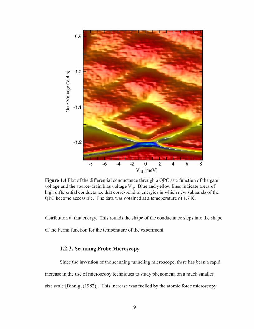
Figure 1.4 shows the differential conductance through the QPC as a function
of its gate voltage and the source-drain voltage Vsd
at a temperature of 1.7 K. Areas
of high differential conductance are shown by the blue and yellow lines. Taking a
vertical line through the data at Vsd
= 0 meV, gives spikes in the differential conductance
corresponding to the addition of each new mode of the QPC. Moving to finite Vsd
,
transport can take place through excited levels in the QPC giving lines of high differential
conductance. These bright lines form diamonds marking the boundary of areas of
constant conductance. By measuring the width of the diamonds, the spacing of the
subbands in the QPC is determined.
The conductance plateaus of the QPC are not well defined when the energy
spacing between the subbands of the QPC becomes smaller than the temperature. This
is because conduction takes place through several subbands and the probability of
transmission through each subband is no longer 0 or 1 but rather given by the electron
€
E = EN + h2kx2
2m
9
distribution at that energy. This rounds the shape of the conductance steps into the shape
of the Fermi function for the temperature of the experiment.
1.2.3. Scanning Probe Microscopy
Since the invention of the scanning tunneling microscope, there has been a rapid
increase in the use of microscopy techniques to study phenomena on a much smaller
size scale [Binnig, (1982)]. This increase was fuelled by the atomic force microscopy
Figure 1.4 Plot of the differential conductance through a QPC as a function of the gate voltage and the source-drain bias voltage V
sd. Blue and yellow lines indicate areas of
high differential conductance that correspond to energies in which new subbands of the QPC become accessible. The data was obtained at a temeperature of 1.7 K.
10
technique, which can image surfaces that are not conducting [Binnig, (1986)]. In recent
years, there have been many groups using low temperature scanning probe microscopes
to study a wide variety of phenomena including standing waves on Cu [Crommie, (1993);
Manoharan, (2000)], carbon nanotubes [Lemay, (2001); Woodside, (2002)], high
temperature superconductors [Hudson, (1999); Pan, (2000)]. One very active area of
research has been on semiconductor heterostructures where research has been focused
in two main areas, electron flow through devices [Eriksson, (1996); Topinka, (2000);
Topinka, (2001); Crook, (2000)] and the quantum hall regime [Tessmer, (1998);
Yacoby, (1999); McCormick, (1999)].
Each of the methods of scanning probe microscopy uses a feedback principle
to perform topographic imaging of the sample. In the case of scanning tunneling
microscopy, the current from the tip to the sample is measured. This is exponentially
sensitive to the distance between the tip and sample, so that it provides a sensitive
measure of the surface topography and atomic resolution can be obtained. However,
this technique requires that the surface is conducting, which is not the case in our
semiconductors where the 2DEG is 57 nm below the surface. In the case of atomic force
microscopy, the force on a small cantilever is measured. By keeping this force constant,
an image of the surface is obtained. The size of the tip determines the resolution of this
technique making atomic resolution difficult but non-conducting surfaces can be imaged.
In order to study the behavior of electrons in a two-dimensional electron gas new
techniques are needed since they are inside the heterostructure.
In the quantum Hall regime, several ways of detecting the properties of the 2DEG
have been developed. These include using a single electron transistor to sense individual

11
charges and map out their location, which has produced images of the quantum hall states
at different filling factors [Yacoby, (1999)]. There are also techniques involving the
measuring of capacitance and compressibility, which leads to information about the local
potential of the electrons [Tessmer, (1998); Finkelstein (2000)]. These techniques work
well at high magnetic filed but are not sensitive to the electron flow without a magnetic
field.
The second class of experiments using scanning probe microscopy techniques
and 2DEGs involve the imaging of electron flow. These techniques all use a perturbation
in the 2DEG to scatter electrons and from the response determine the pattern of
electron flow. This technique has been applied to the flow through a large channel
[Eriksson, (1996)], flow from a quantum point contact [Topinka, (2000); Crook, (2000a)],
bending due to magnetic field [Crook, (2000b)], and electron flow in a 2DEG
[Topinka, (2001)]. In the rest of this thesis, this technique and variations of it will be
applied to a new set of devices to understand the electron flow through them.
1.3. Outline
This thesis presents results from experiments imaging coherent electron flow.
All of the results presented were obtained using a liquid-Helium cooled scanning probe
microscope [Topinka, (2002)]. The scanning probe microscope tip is used to probe the
pattern of electron flow through a two-dimensional electron gas formed in a
GaAs/AlGaAs heterostructure. Figure 1.5 shows images of electron flow from the
(a) first, (b) second, and (c) third mode of a QPC located 700 nm past the right edge of
the images. The modal pattern of the electron flow from the QPC is visible along with
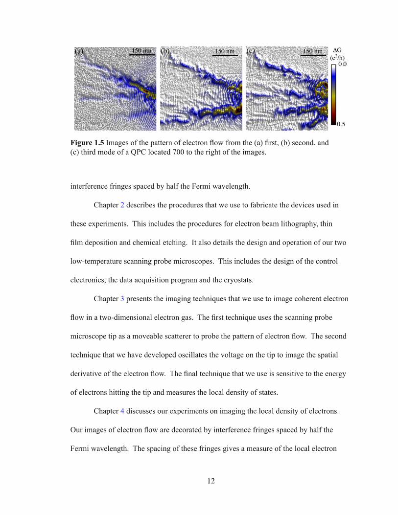
12
interference fringes spaced by half the Fermi wavelength.
Chapter 2 describes the procedures that we use to fabricate the devices used in
these experiments. This includes the procedures for electron beam lithography, thin
film deposition and chemical etching. It also details the design and operation of our two
low-temperature scanning probe microscopes. This includes the design of the control
electronics, the data acquisition program and the cryostats.
Chapter 3 presents the imaging techniques that we use to image coherent electron
flow in a two-dimensional electron gas. The first technique uses the scanning probe
microscope tip as a moveable scatterer to probe the pattern of electron flow. The second
technique that we have developed oscillates the voltage on the tip to image the spatial
derivative of the electron flow. The final technique that we use is sensitive to the energy
of electrons hitting the tip and measures the local density of states.
Chapter 4 discusses our experiments on imaging the local density of electrons.
Our images of electron flow are decorated by interference fringes spaced by half the
Fermi wavelength. The spacing of these fringes gives a measure of the local electron
Figure 1.5 Images of the pattern of electron flow from the (a) first, (b) second, and (c) third mode of a QPC located 700 to the right of the images.

13
density. By measuring the change in wavelength as a function of back gate voltage, the
results are compared with a capacitor model. We also show that images of electron flow
become more diffuse as the density is reduced because the mean free path of the electrons
is reduced.
Chapter 5 describes our measurements of the electron-electron scattering length
in the two-dimensional electron gas. We demonstrate a technique that is sensitive to
whether or not an electron has scattered. By accelerating the electrons across a quantum
point contact, we decrease their scattering length. This decrease in scattering length is
measured by our images of electron flow. The results for a variety of distances and Fermi
energies are shown and all agree with theory for electron-electron scattering in a 2DEG.
Chapter 6 shows images from a series of experiments on electron optics devices.
These are devices that control the flow of electrons using electrostatic gates in analogy
to switches and lenses in optics. We show images of electron flow from a triangular
electrostatic gate, which acts as a switch. We use a round gate as a defocusing lens and as
a circular scatterer for electron waves. We also fabricated a narrow channel to guide the
electrons and study the potential profile from the electrostatic gate.
Chapter 7 examines the origin of the interference fringes that are seen in all of our
images of coherent electron flow. The fringes arise from interference of electron waves
backscattered from the tip with backscattered waves from impurities that are near the
same distance from the QPC as the tip. This is confirmed by using a small reflecting arc,
which acts like a large number of impurities, to enhance the interference fringes at the
same radius as the arc. The interference fringes move with the position of the reflector
as controlled by its voltage. We have also found that enhanced backscattering from the

14
arc enhances the interference fringes. In the last section, we show that the interference
fringes are more robust to thermal smearing near the radius of the reflector.
Chapter 8 presents some conclusions for the experiments described in this thesis.
It also discusses some future experiments that can be done using our two low temperature
scanning probe microscopes. These include new experiments made possible by the
construction of our He-3 microscope that can reach much lower temperatures.
15
Chapter 2
Experimental Techniques
This chapter includes two main parts; the first half discusses the procedures
needed to fabricate the samples used in our imaging experiments. The second half of
the chapter covers the design and operation of our two low-temperature scanned probe
microscopes (SPMs). Section 2.1 outlines the procedures used to make samples and
prepare scanning probe microscope tips. The first part of section 2.1 covers the basic
preparation of the samples including cleaving (section 2.1.1), cleaning (section 2.1.2),
spinning PMMA (section 2.1.3), and writing patterns using the scanning electron
microscope (section 2.1.4). The second part of this section includes details of chemical
etching (section 2.1.5), depositing metal (section 2.1.6), annealing ohmic contacts
(section 2.1.7) and wirebonding (section 2.1.8). The last part of section 2.1 in section
2.1.9 discusses the procedure used to coat the scanning probe tips with Cr. The rest of
the chapter discusses the design and operation of the experimental equipment used in our
experiments. The design of the He-4 system has been covered in previous theses, but
the main points will be briefly highlighted in section 2.2. Much of the rest of the chapter
is devoted to the design of the new He-3 system and the electronics for both SPMs.
Section 2.3 has a discussion of the new SPM including the design of the cryostat, magnet
and sample stick. Section 2.4 includes descriptions of all of the electronics needed to run
either of the SPMs. There is a discussion of the new digital to analog control circuitry
used by both SPMs in section 2.4.1. This allows faster and higher resolution scans to be
16
taken. After this, there is a discussion of the other electronics that are necessary for using
the SPM including the surface flattening box (section 2.4.2), the feedback circuit (section
2.4.3), the high voltage amplifiers (section 2.4.4), summing amplifiers (section 2.4.5), and
the computer program that is used for SPM control and data acquisition (section 2.4.6).
2.1. Sample Fabrication
This section details the procedures necessary to make the samples used in the
imaging experiments in this thesis. All of our samples use two-dimensional electron
gases formed in AlGaAs/GaAs heterostructures. We get the samples as unprocessed
wafers from Art Gossard’s group at the University of California—Santa Barbara. All
of the processing is done in the two cleanrooms in Gordon McKay Lab. The procedure
for defining a device consists of the following steps: cleaving a sample, creating a mesa,
making ohmic contacts and lastly writing the electrostatic gates. Each of these steps
requires several procedures, which will be outlined in the remainder of the chapter.
The last two steps needed before imaging electron flow are wirebonding the sample
and coating the SPM tip with Cr. Much of the information about sample fabrication
is covered in other theses from our group. Lester Chen [Chen, (2001)] gives detailed
procedures on how to use most of the pieces of equipment while Mark Topinka
[Topinka, (2002)] covers some of the specific requirements of the SPM experiments.
2.1.1. Cleaving Samples
The samples generally arrive in our lab as half of a 2 inch wafer. For each of our
experiments we only need a very small piece of this wafer so it is necessary to cleave the

17
wafer into small pieces. In order to cleave the wafer, the necessary tools are a diamond
scribe, Q-tip, ruler, glass slide, dust mask and ultra-high purity nitrogen. Make sure that
you are wearing the mask because GaAs dust is hazardous. If you are really concerned
about the dust you can even do this procedure in the fume hood. It is important that you
know which side of the wafer is the front. Before making any scribes ensure that you
can identify the front and if necessary make a small diagonal scratch on the back1. First
measure the size of the wafer that is desired and then make a scratch in the wafer with
the diamond scribe. GaAs readily breaks along its crystal axes so it is only necessary to
make a very small scratch on the edge of the wafer. Blow off the dust before breaking
the piece to keep the surface from being scratched. Put the wafer on the glass slide with
the piece to break off hanging over the edge. Then press down with a Q-tip and the piece
will cleave along this line. Blow off the dust and repeat this process until you have the
desired size and number of samples. For the SPM it is best to use pieces that are about
2 x 3 mm. If they are too big it is very difficult to attach them to the sample holder or
they may not even fit. If the samples are much smaller they are hard to work with for the
rest of the processing steps, especially the spinning of PMMA.
2.1.2. Cleaning
The samples are cleaned in three successive solvents, Trichloroethylene (TCE),
acetone and methanol. The first step is to put the samples in small Teflon beakers in
boiling TCE for 5 minutes. Make sure that the Teflon beakers have holes in them to let
1 For the wafers with a back gate it is fairly easy to tell the front from the back because the front is smooth while the back is rougher and a different color.

18
the TCE wash over the samples. Then transfer the samples to plastic beakers filled with
acetone and ultrasound for 5 minutes2. The last step is to use a new set of plastic beakers
filled with methanol. Put the samples in these beakers and then into the ultrasound for
five more minutes. After this is done the samples should be blown dry with ultra-high
purity nitrogen and they are ready for spinning. This procedure is repeated before each
spinning step but the TCE portion is usually skipped.
2.1.3. Spinning
In order to write a pattern on the samples it is necessary to spin on a resist. Since
all of our writing steps are done in the SEM we use Polymethylmethacrylate (PMMA)3,
which is an electron beam sensitive resist. Locations that are exposed to the e-beam have
their bonds broken and can be developed away more easily. Depending on the fabrication
step either two or three layers are used. There are two reasons for using multiple layers,
the first one is to provide an undercut that facilitates the lift-off of the metal deposited.
To produce this undercut, a lighter PMMA is spun on for the bottom layers. This light
PMMA is more easily exposed which creates a larger developed area and hence an
undercut. Only the top most layer is a heavy PMMA. The other reason to use multiple
layers is that the PMMA tends to crack when drying. Each single layer has line defects,
but two layers will only have point defects where the lines intersect. By using three
layers there should be no defects unless you are very unlucky. We use 2% (by volume)
3 MicroChem Corporation, 1254 Chestnut St., Newton, MA 02464
2 Make sure that all the plastic beakers are labeled with their contents and that you properly dispose of them when you are finished. Otherwise, the hood is filled with beakers that contain unknown chemicals.

19
496K PMMA in Anisole for the light layer and 2% 950K PMMA in Anisole for the
heavy layer. The procedure is very simple for spinning the chips. It is done in the inner
cleanroom in the basement where there are two spinners and hot plates. Figure 2.1 shows
the setup of one of the spinners and hot plates. Set the hotplate to 180 °C and wait for it
to warm up. Set the spinner to go at 500 rpm for 5 seconds followed by 4000 rpm for 30
seconds. This should be one of the preprogrammed recipes. While the chip is spinning
slowly, use a pippet to put a drop of PMMA on it. After it is finished spinning move it to
the hotplate and let it bake for at least 5 minutes. Repeat the procedure until the desired
number of layers are spun.
Figure 2.1 Setup of the spinner system in the basement cleanroom. The spinner is recessed in the back with a hotplate on the right. The controller is on the far right and there is a foot pedal to start and stop the spinner, which is not shown.
20
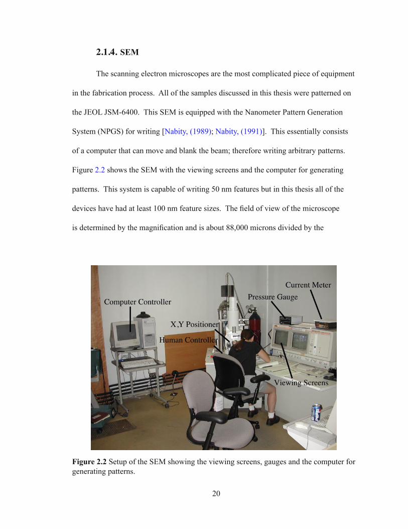
2.1.4. SEM
The scanning electron microscopes are the most complicated piece of equipment
in the fabrication process. All of the samples discussed in this thesis were patterned on
the JEOL JSM-6400. This SEM is equipped with the Nanometer Pattern Generation
System (NPGS) for writing [Nabity, (1989); Nabity, (1991)]. This essentially consists
of a computer that can move and blank the beam; therefore writing arbitrary patterns.
Figure 2.2 shows the SEM with the viewing screens and the computer for generating
patterns. This system is capable of writing 50 nm features but in this thesis all of the
devices have had at least 100 nm feature sizes. The field of view of the microscope
is determined by the magnification and is about 88,000 microns divided by the
Figure 2.2 Setup of the SEM showing the viewing screens, gauges and the computer for generating patterns.
21
magnification. The design of patterns is done using DesignCad for the PC. Each layer
in the DesignCad file can correspond to a different magnification and current setting on
the SEM. Each magnification and current setting must be manually set by the user. The
most useful way to discuss the procedure for using the SEM is to write out the necessary
steps in a list, which is included in appendix A.
After the chip is written and the PMMA has been exposed it must be developed.
This is done by putting the sample in a mixture of isopropyl alcohol (IPA), methyl
isobutyl ketone (MIBK) and methyl-ethyl ketone (MEK). The standard recipe for the
developing solution is 375 ml IPA, 125 ml MIBK and 6.5 ml MEK. First rinse the
sample with IPA to remove any carbon paint that is on it. Then put it in the developing
solution for 1 minute before rinsing it in IPA to stop the developing. Look at the sample
in the optical microscope to see if the features have been developed. If not the sample
can be developed for a longer time. The longer the sample is in the developer the wider
the features become because the PMMA is slowly developed near the exposed areas.
2.1.5. Wet Etching
In order to define mesas for our samples we use a wet etch procedure. The mesas
allow the electrostatic gates to run off of the edge of the device without contacting the
back gate. It also allows separate ohmic contacts to be made to the device area and the
back gate. The etch mixture is a combination of Citric Acid and Hydrogen Peroxide.
The Citric acid is already mixed with water at the ratio of 1:1 by weight. This is then
combined with the Hydrogen Peroxide with ten parts citric acid for each part Hydrogen
Peroxide by volume. The procedure is described in detail in Mark Topinka’s thesis
22
[Topinka, (2002)]. The basic steps are to put the sample in HCl followed by NH4OH to
clean off any oxides that might be on it. Both of these should be diluted with water by a
factor of 5. The sample spends 5 seconds in each followed by a beaker of water. Then
put the sample into the etch mixture, which should be heated to 50 °C, for the desired
amount of time. The etch is quenched by putting the sample in water. The etch rates for
GaAs and AlGaAs are about 100 Å /s and 20 Å /s. In order to define the etch trenches
separating the active device area from the back gate contacts, I usually dip the sample in
the citric etch for 15 seconds. After etching, the PMMA can be removed by soaking the
sample in acetone.
2.1.6. Thermal Evaporator
There are two different thermal evaporating systems that we use. There is one
in the downstairs cleanroom for the Cr-Au gates and another one upstairs for the Ohmic
contacts4. Figure 2.3 shows both the inside and outside of the new evaporator in the
downstairs cleanroom. They both have fairly similar procedures to use them so I will
just give the general steps necessary to operate them. The first step is to dip the samples
in NH4OH for 5 seconds to clean their surface, allowing the metal to stick to them better.
Then attach them with carbon paint to the Cu sample stage. Make sure that you use
the correct stage for the evaporator. Then go into the cleanroom and vent the chamber.
Load the stage and put the necessary arms, boats and metals into the evaporator. For
ohmic contacts you will need, Ni, Au and Ge. For the gates you need Cr and Au. Close
4 With the continued purchase of equipment by CIMS the thermal evaporators are constantly changing. Check the signs on the evaporators to know, which metals can be evaporated.

23
the chamber and start the roughing pump. Once the pressure reaches 200 mTorr, close
the roughing valve, turn off the pump and open the high vacuum valve. This starts the
cryopump. Once the pressure reaches the 10-6 torr range, you can degas the filament for
one minute. Now is also a good time to check the contacts on the boats. Slowly turn
up the current and watch the boats. They should start to glow in the center first, if they
glow at one end first this is a sign that there is a bad connection and you should reattach
them. It is also necessary to heat up the Cr rod for about 30 seconds to let it outgas and
remove the oxide from it. Once the pressure reaches a few times 10-7 torr you are ready
to evaporate. This takes about 15 minutes in the new evaporator downstairs and about an
hour in the one upstairs. Make sure that the correct parameters are set for the metal that
you are depositing and then slowly turn up the current until it starts to evaporate. Once
about 50 Å have been deposited, open the shutter and start the deposition on the sample.
Once you have finished depositing metal, let the chamber cool for a few minutes and then
close the high vacuum valve and vent it. Take out the sample stage and pump back down
Figure 2.3 Shows the new thermal evaporator in the downstairs cleanroom used for depositing gates. The control system is shown in the left hand picture. The right hand picture shows the inside of the evaporator including the position of the boats.

24
the system for the next user. Remove the sample from the stage and put it in a beaker of
acetone to lift-off the PMMA. You can check the progress of the lifting off in the optical
microscope. However, the sample must stay in acetone or the PMMA will not lift off. If
the PMMA is not lifting off, a small amount of time in ultrasound will help but be careful
not to do it for too long or the metal may come off also.
For ohmic contacts the recipe that we use is the following: 50 Å of Ni, 50 Å of
Au, 250 Å of Ge, 400 Å of Au, 100 Å of Ni and 400 Å of Au. This creates a eutectic
mixture that allows for easy annealing of the contacts. For the gates, I usually deposit
100 Å of Cr then open the chamber and cover the device. Then I deposit a further 50 Å
of Cr and 400 Å of Au on the pads for wirebonding. This makes it easier for the SPM tip
to get into the device and avoids problems with the Au tending to form balls.
2.1.7. Annealing
After lifting off the excess metal and PMMA, the ohmic contacts are ready to be
annealed. This is done with our thermal annealer that was built by Alex Rimberg and
described in his thesis [Rimberg, (1992)]. It was originally built for annealing Indium
contacts but is now almost exclusively used for NiAuGe ohmics. Figure 2.4 shows the
basic setup of the annealing system. There is a cylinder of forming gas, (80% He/20% H)
which flows through the box to keep the sample from oxidizing during the annealing
process. The gas flow rate should be adjusted so that the bottom of the silver ball is at
the 3 on the flow meter. The sample sits on a strip of Nichrome that is heated using the
two transformers. The only change to the annealer is that the Nichrome was replaced
and the thermometer underneath was reattached5. The recipe for annealing the samples

25
is as follows: one minute at 110 °C to boil off any water vapor, 10 seconds at 260 °C
to warm everything up followed by 10 seconds at 380 °C. This last step is the critical
one because it is when all of the annealing takes place. For the samples with a back
gate, it is very important not to exceed 380 °C because the ohmics tend to anneal too
much and contact the back gate making the sample not usable. However, it is necessary
to get the temperature to 380 °C because this is just above the temperature where the
Au/Ge mixture melts. To get a faster reading of the temperature you can attach a Fluke
multimeter to the two pins of the thermometer and measure the voltage. It is usually a
5 The Nichrome strip was bought from MWS Wire Industries, 31200 Cedar Valley Dr. Westlake Village, CA 91362. There still remain many feet of it for future use. It is a too thick for the transformers to be able to heat sufficiently so it has to be thinned before being used. The thermometer was spot welded to the back of the strip in the student shop in Lyman.
Figure 2.4 The thermal annealing setup is shown with the forming gas, thermometer and transformer.

26
good idea to rotate the sample by 180 degrees and repeat the process to ensure that the
contacts are well annealed. Using this recipe will not produce ohmics that look like
cheese pizza as occurs for higher temperatures6. I have found that this recipe produces
working ohmics nearly every time and they are never shorted to the back gate. If testing
the ohmics for shorts to the back gate at room temperature it is important not to have light
on the sample. Since the GaAs is photoconductive, a false reading of the resistance will
be obtained.
2.1.8. Wire bonding
The last step in preparing the sample is to attach it to the sample holder and wire
bond to all of the pads. The arrangement of the pads and wire bonds is very important
because none of the wires can cross the device. If this occurs the tip will not be able to
reach the device. Figure 2.5 shows how the sample is mounted on the sample holder.
First a piece of lens paper is put on the sample holder using GE varnish to insulate the
sample from the holder. The sample is placed on top of this with the device near the
center. To make the arrangement of the wire bonds simpler, all of the bonding pads are
placed along the bottom of the sample. Then the gold wire can just go from the sample
holder to the pads. There are a total of 12 pads on the sample holders for both the He-3
and He-4 SPMs.
To get the wire bonder to work properly, it is necessary to thread the gold wire
correctly. For the tips that we use, the wire should go under the spool and into the second
6 Other theses said that this was the look of ohmics that were well annealed and that worked.

27
hole on the arm, the one farthest from you. Then it goes down and through the clamp and
into the tip. Make sure that the heater is on to heat the sample to 80 °C. It works best to
use a medium setting on the force, the maximum time and 2.0 on the power. Sometimes,
the power can be turned higher for the bonds on the sample holder. In order for the bonds
to work, a small section of gold should be sticking out of the tip before starting to make
a bond. If the wire does not feed properly between bonds, the tail adjustment can be
changed to increase the amount that feeds.
2.1.9. Coating Tip
The one other time that we need to use the evaporator is when coating the tip
with Cr. During the course of the deposition it is necessary to rotate the tip in order
to uniformly coat it. This evaporation is done in the “clean” Sharon evaporator in the
Figure 2.5 Sample holder for the new He-3 SPM showing the position of the sample and bonding pads.

28
upstairs cleanroom because it has a rotating feedthrough. Figure 2.6 shows the stage used
to rotate the tip in the evaporator. The stage attaches to the evaporator the same as the
ordinary stages but there has to be another connection made to rotate it. This is done by
a flexible braid that attaches to both the stage and the rotating feedthrough. The Cr rod
should be positioned as near to the edge of the evaporator as possible to get a good angle
to coat the tip. This ensures that the Cr comes from the side and not directly below the
tip. I coat the tip with 100 Å of Cr, rotating the stage about one revolution per 5 seconds.
The tip has to be mounted so that only the end of the cantilever is coated. If
both arms of the cantilever are coated the resistance will change. This makes the
piezoresistive cantilevers not work anymore because the Cr determines their resistance
instead of the piezoresistive Silicon. This failure shows up when the cantilever is put in
Figure 2.6 Mounting stage for coating tips with Cr. This stage attaches to the evaporator and can be rotated using a feedthrough. The cantilever is positioned so that all but the very end is covered by the mask..

29
the whetstone bridge and the measured signal is very noisy. To avoid this problem only
a small section of the cantilever is exposed beyond the end of a piece of the metal mask.
The position of the cantilever can be adjusted in all three directions by screws on the
rotating stage. This is done while looking through a microscope in order to minimize the
amount of the cantilever that is exposed.
2.2. He-4 System
Most of the design of this system is covered in the theses of Mark Eriksson
and Mark Topinka [Eriksson, (1997); Topinka, (2002)]. Therefore this section will
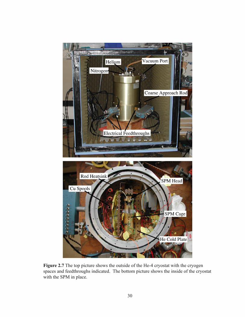
just highlight some of the important considerations when using this SPM. Figure 2.7
shows the He-4 SPM’s cryostat. It consists of a large vacuum space for the SPM along
with helium and nitrogen reservoirs. There are three electrical feedthroughs into the
vacuum space along with a rotating rod that is the coarse approach mechanism. One
of the connectors is a 24 pin Fischer connector for the leads going to the sample. Only
twelve of these leads are wired all the way to the sample. The second connector is an
18 pin Fischer connector that goes to the cantilever bridge circuit, LED, and the two
thermometers. The last connector is for the high voltage lines going to the piezotube.
Since the SPM is in vacuum, care must be taken to properly heat sink all of the
leads that come into the dewar. This is accomplished through the use of high resistance
wire, which has a low thermal conductivity. After a section of this wire, there are copper
wires wrapped around copper spools attached to the cold plate. This thermally anchors
the wires at the temperature of the cold plate. The heat sinking of the coarse approach
rod is more difficult because of the requirement that it can rotate. Specially designed
30
Figure 2.7 The top picture shows the outside of the He-4 cryostat with the cryogen spaces and feedthroughs indicated. The bottom picture shows the inside of the cryostat with the SPM in place.

31
clamps were built to heat sink the rod to both the liquid nitrogen bath and the He cold
plate. Figure 2.8 shows the design of these two clamps. The clamps are a piece of
copper with a hole drilled out for the rod to slide through. Then a slit is cut through the
piece and a screw hole drilled into it so it can be screwed down tightly to the rod. Then a
thick copper wire goes from this piece to the cold plate. This design gives a large contact
area between the rod and clamp while still allowing the rod to rotate.
The cooling procedure for this cryostat is fairly complicated compared to the
new He-3 system due to the vacuum space and nitrogen jacket. After aligning the
SPM, the radiation shields have to be put on. There are two radiation shields, one at He
temperature and another at Nitrogen. Then the top must be put on taking care to make a
good vacuum seal with the large O-ring. Then the cryostat has to be flipped over before
pumping out the vacuum space. It is a good idea to check that the position of the SPM
has not moved significantly during the process of flipping the cryostat. It takes around 90
minutes to two hours to pump out the cryostat with the turbopump cart. Then it can be
Figure 2.8 Design of clamps that go on the coarse approach rod. The clamp is slid on the rod and then tightened using the screw. The Cu wire is attached to the cold plate to thermally anchor the rod.
32
filled with liquid nitrogen in both the Nitrogen jacket and the helium space. After about
two hours it will have cooled enough that helium can be put into the center space. An
indication that it is cold is when there is no longer frost on the cover of the helium space.
First blow out all of the Nitrogen so that solid nitrogen does not form in the Helium space
causing the cryostat not to cool. Then fill it with Helium. It takes about two more hours
for the SPM to reach 4.2 K. Once everything is cold, the Helium and Nitrogen last about
12 hours before needing to be refilled. The helium can be pumped on to lower the sample
temerature to 1.7 K. However, when doing this, the helium only lasts about 8 hours.
2.3. He-3 System
This section describes our group’s new SPM, which was built to achieve lower
temperatures than accessible with our Helium-4 system. The goal was to be able to reach
400mK with this system but unfortunately we have not run it yet as a Helium-3 system.
Even, as a Helium-4 system it has several advantages over the older one. This cryostat
has a superconducting solenoid, which provides a perpendicular field that is rated up
to 7 Tesla. In the initial test of the magnet, I was able to run it above 8 Tesla without it
quenching. It also has the ability to use a magnet providing a parallel field of up to about
3 Tesla. It also has a much longer hold time, from initial tests it appears that the dewar
can go for about 60 hours without refilling. This is compared to only 12 hours with the
old system, which uses both Helium and Nitrogen. The last significant advantage is the
turn around time, it is now possible to change a sample within just a couple of hours as
compared to almost two days with the old system.

33
2.3.1. Cryostat Design
The design of the cryostat was modeled from the other two He-3 cryostats that our
group uses. Figure 2.9 is a drawing of the dewar and the support structure for holding
the magnet. The dewar has a superinsulation jacket with a 15 liter belly for holding the
liquid helium. There is a small well that the magnet sits in with the SPM inside. We built
the dewar fairly tall to lengthen its neck and thus lessen the heat load down the dewar due
to radiation. The magnet support is built around three stainless steel tubes that attach to a
support plate at the bottom. As you go down the magnet support there are a series of Cu
baffles to reduce the radiation on the Helium.
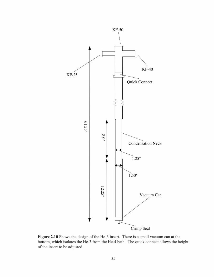
The Helium-3 insert is shown in Figure 2.10. It is a very simple design, which
has a small vacuum can at the bottom with a condensation neck just above. This vacuum
can was pumped out before the first use and sealed by crimping and soldering the Cu
tube7. The idea behind the insert is that He-3 gas comes down the insert and hits the
condensation neck immersed in pumped He-4, which liquefies the He-3 and it falls
into the bottom of the vacuum can. In the vacuum can, it is isolated from the He-4 so
it can be further cooled. Once all of the He-3 is liquefied, it is pumped on to reduce its
temperature down to about 400mK. The insert is made of thin walled stainless steel,
0.020”, to minimize the heat load on the He-4 bath. The cryostat, magnet support and
He-3 insert were built by Precision Cryogenics8.
The magnet support piece has been wired for a superconducting solenoid. There
7 We had a lot of trouble finding the proper tool for making the crimp seal. We finally borrowed one from Dave McCarthy at Varian Vacuum, 800-882-7426 ext 5768. The tool is made by CHA Industries and its part number is POD-375. I practiced making the crimp seal on another piece of copper tubing and it worked all 10 times that I tried.

34
Figure 2.9 Drawing of the He-3 SPM cryostat and the magnet support. The cryostat has a superinsulation jacket with a 15 liter belly for the liquid Helium. The magnet support piece has 3 stainless steel tubes supporting the magnet with 7 Cu baffles to reduce the radiation.
8 Precision Cryogenics, 7804 Rockville Rd, Indianapolis, Indiana 46214. Our group has had good luck with their work in the past but on this project they forgot to drill a hole in the bottom piece of the magnet support. So there was no way for the He-3 insert to go all the way into the cryostat.
35
Figure 2.10 Shows the design of the He-3 insert. There is a small vacuum can at the bottom, which isolates the He-3 from the He-4 bath. The quick connect allows the height of the insert to be adjusted.
36
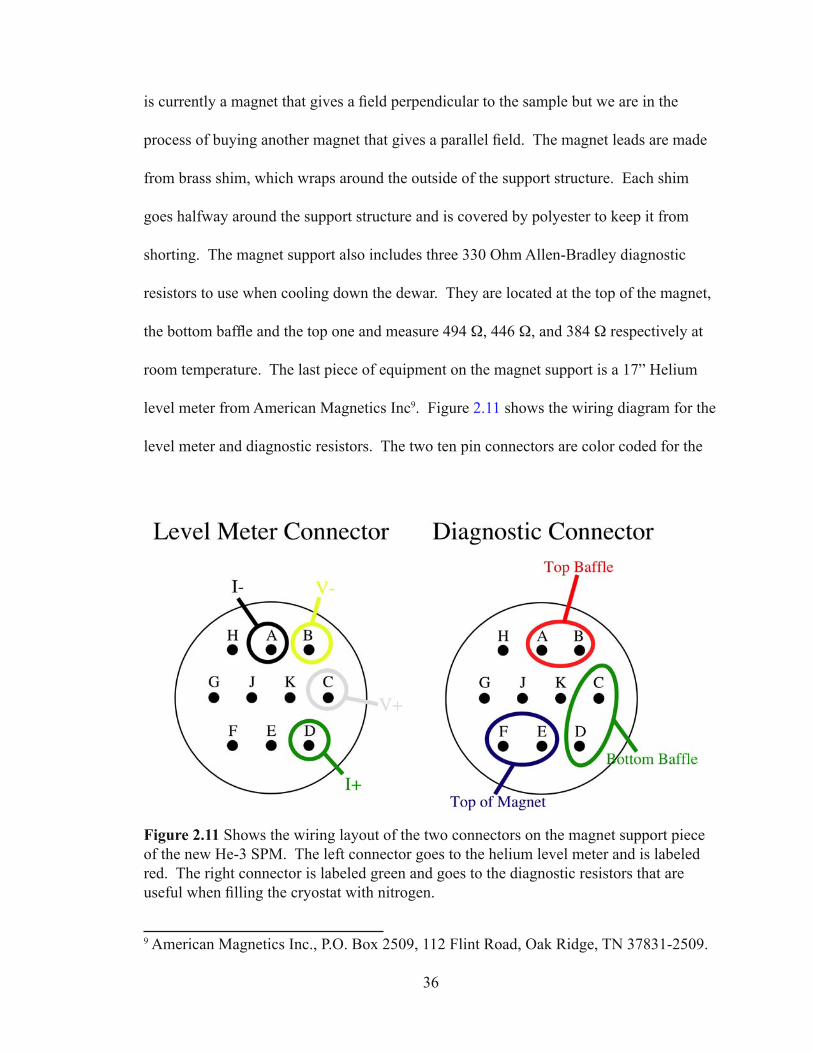
is currently a magnet that gives a field perpendicular to the sample but we are in the
process of buying another magnet that gives a parallel field. The magnet leads are made
from brass shim, which wraps around the outside of the support structure. Each shim
goes halfway around the support structure and is covered by polyester to keep it from
shorting. The magnet support also includes three 330 Ohm Allen-Bradley diagnostic
resistors to use when cooling down the dewar. They are located at the top of the magnet,
the bottom baffle and the top one and measure 494 Ω, 446 Ω, and 384 Ω respectively at
room temperature. The last piece of equipment on the magnet support is a 17” Helium
level meter from American Magnetics Inc9. Figure 2.11 shows the wiring diagram for the
level meter and diagnostic resistors. The two ten pin connectors are color coded for the
9 American Magnetics Inc., P.O. Box 2509, 112 Flint Road, Oak Ridge, TN 37831-2509.
Figure 2.11 Shows the wiring layout of the two connectors on the magnet support piece of the new He-3 SPM. The left connector goes to the helium level meter and is labeled red. The right connector is labeled green and goes to the diagnostic resistors that are useful when filling the cryostat with nitrogen.

37
resistors, green, and the level meter, red.
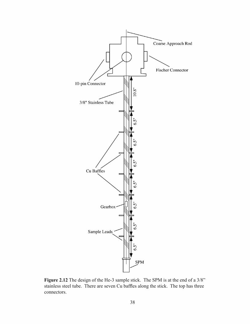
2.3.2. Sample Stick
The last piece of the cryostat design is the sample stick, which goes inside the
He-3 Insert. Figure 2.12 shows the sample stick with the connectors at the top, wires
running along the central tube and a gearbox for the coarse approach rod. There are three
connectors on the tip of the stick, which go to the sample, piezotube and miscellaneous
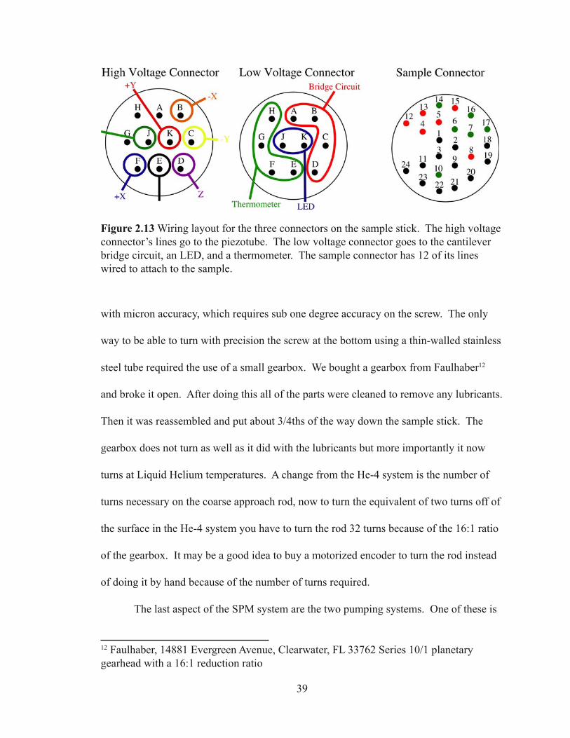
low voltage connections. Figure 2.13 shows the layout of the three connectors at the top
of the sample stick. The sample leads come from a 24 pin Fischer connector10. There
are currently 12 leads wired all the way to the bottom of the stick but the other 12 are
wrapped up near the top of the stick for future use. The sample leads are grouped into 3
sets of 36 gauge Quad Lead phosphor bronze wire from Lakeshore Cryogenics11. There
are seven high voltage lines of which 5 are used by the piezotube. The other two lines
can be used for oscillating the tip or other high frequency applications. Each of the
high voltage lines is wired with ultra miniature Stainless Steel coax to accommodate
both high voltage and high frequency. The last set of wires is for the cantilever bridge
circuit, an LED, and other diagnostic wiring. There are a total of 10 of these 36 gauge
phosphor bronze wires of which 6 are currently used. Perhaps the most difficult aspect
of the sample stick was the construction of the coarse approach rod for the SPM. Since
we need to be able to turn one of the screws of the SPM head when it is cold, we need a
long rod to reach the bottom of the insert. We need to be able to set the height of the tip
11 Lakeshore Cryotronics, 64 East Walnut St., Westerville, OH 43081 Quad Lead Wire QL-36, Coaxial Wire CC-SS and phosphor bronze wire NM-36.
10 Fischer Connectors, Atlanta, GA 30346, www.fischer.com
38
Figure 2.12 The design of the He-3 sample stick. The SPM is at the end of a 3/8” stainless steel tube. There are seven Cu baffles along the stick. The top has three connectors.
39
with micron accuracy, which requires sub one degree accuracy on the screw. The only
way to be able to turn with precision the screw at the bottom using a thin-walled stainless
steel tube required the use of a small gearbox. We bought a gearbox from Faulhaber12
and broke it open. After doing this all of the parts were cleaned to remove any lubricants.
Then it was reassembled and put about 3/4ths of the way down the sample stick. The
gearbox does not turn as well as it did with the lubricants but more importantly it now
turns at Liquid Helium temperatures. A change from the He-4 system is the number of
turns necessary on the coarse approach rod, now to turn the equivalent of two turns off of
the surface in the He-4 system you have to turn the rod 32 turns because of the 16:1 ratio
of the gearbox. It may be a good idea to buy a motorized encoder to turn the rod instead
of doing it by hand because of the number of turns required.
The last aspect of the SPM system are the two pumping systems. One of these is
Figure 2.13 Wiring layout for the three connectors on the sample stick. The high voltage connector’s lines go to the piezotube. The low voltage connector goes to the cantilever bridge circuit, an LED, and a thermometer. The sample connector has 12 of its lines wired to attach to the sample.
12 Faulhaber, 14881 Evergreen Avenue, Clearwater, FL 33762 Series 10/1 planetary gearhead with a 16:1 reduction ratio
40
for pumping on the He-4 bath to cool it to 1.7K. This is necessary so that the He-3 gas
will liquefy as it passes the condensation neck. The second system is for pumping on the
He-3 to further cool it to around 400 mK. This system must be leak tight and have the
exhaust go back into the He-3 dumps so as not to lose the valuable He-3 gas. The He-
4 system consists of an Alcatel 2033SD pump, which is a two-stage rotary vane pump
capable of pumping 33 m3/hr13. This is connected to the cryostat via a KF-40 tube with a
pressure gauge on this line. The pressure gauge is a Leybold DV1000 diaphragm gauge.
This gauge is used since its reading is insensitive to the composition of the gas. The He-
3 gas handling system is essentially a copy of the previous system that we have for the
group’s other He-3 cryostats [Hopkins, (1990)]. However, the pump has been changed to
an Alcatel 2015H1, which is a sealed rotary vane pump. The capacity of the dumps has
also been increased to 50 L to accommodate the larger volume of He-3. There is a total
of 40 liters of He-3 in the system giving a reading of 775 mbar on the gauge.
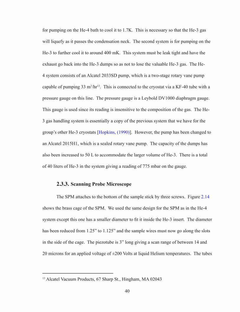
2.3.3. Scanning Probe Microscope
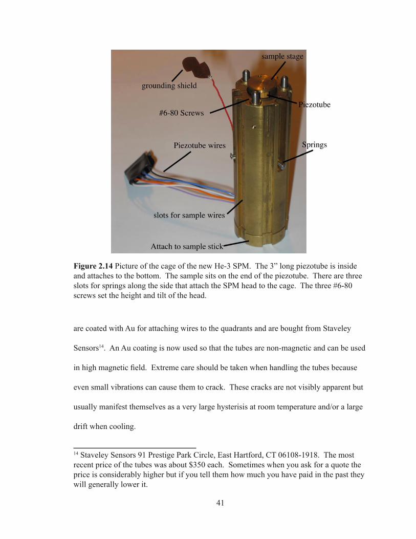
The SPM attaches to the bottom of the sample stick by three screws. Figure 2.14
shows the brass cage of the SPM. We used the same design for the SPM as in the He-4
system except this one has a smaller diameter to fit it inside the He-3 insert. The diameter
has been reduced from 1.25” to 1.125” and the sample wires must now go along the slots
in the side of the cage. The piezotube is 3” long giving a scan range of between 14 and
20 microns for an applied voltage of ±200 Volts at liquid Helium temperatures. The tubes
13 Alcatel Vacuum Products, 67 Sharp St., Hingham, MA 02043
41
are coated with Au for attaching wires to the quadrants and are bought from Staveley
Sensors14. An Au coating is now used so that the tubes are non-magnetic and can be used
in high magnetic field. Extreme care should be taken when handling the tubes because
even small vibrations can cause them to crack. These cracks are not visibly apparent but
usually manifest themselves as a very large hysterisis at room temperature and/or a large
drift when cooling.
Figure 2.14 Picture of the cage of the new He-3 SPM. The 3” long piezotube is inside and attaches to the bottom. The sample sits on the end of the piezotube. There are three slots for springs along the side that attach the SPM head to the cage. The three #6-80 screws set the height and tilt of the head.
14 Staveley Sensors 91 Prestige Park Circle, East Hartford, CT 06108-1918. The most recent price of the tubes was about $350 each. Sometimes when you ask for a quote the price is considerably higher but if you tell them how much you have paid in the past they will generally lower it.

42
Figure 2.15 shows the head of the SPM with a tip in place. The head is held in
contact with the cage by three springs, which attach to the hooks. There are three #6-80
screws that set the height and tilt of the tip and rest in the grooves of the head. Alignment
in the x, y direction is done at room temperature by turning the two adjustment screws
on the side of the head. Only the screw for adjusting the height needs to be turned at low
temperatures so this is the one that must be aligned with the coarse approach rod. The
cantilevers are Piezolevers from Park Scientific Instruments15. We coat the ends of the
cantilever with chrome to create a conducting tip to use in imaging electron flow.
Figure 2.15 The head of the He-3 SPM. The tip sits on the end of a movable shuttle whose position is controlled by the two coarse adjustment screws. There are three hooks for springs to keep the head attach to the cage. There are also three slots for the screws to rest in that adjust the height and tilt of the cantilever.

43
The real test of any SPM is whether it can take good images. Figure 2.16 is a
topographic image of a test pattern. This image was taken in the He-3 system. We have
also taken images with a perpendicular magnetic field of 7 Tesla and saw no evidence that
the magnetic field affected our ability to acquire images.
2.4. Electronics
The other main aspect of building the new SPM is the electronics to control the
piezotube and sample. There has been a considerable effort to build the electronics
necessary for the new SPM as well as updating the ones on the He-4 system. The
Figure 2.16 Topographic scan showing an image in the new He-3 system. The image is of one of the alignment markers.
15 Over the course of my time in the lab, Park has been bought twice and is now part of the Digital Instruments group of companies. The website for information about the cantilevers is www.spmprobes.com
44
electronics for running the two SPMs are nearly duplicates of each other. This allows
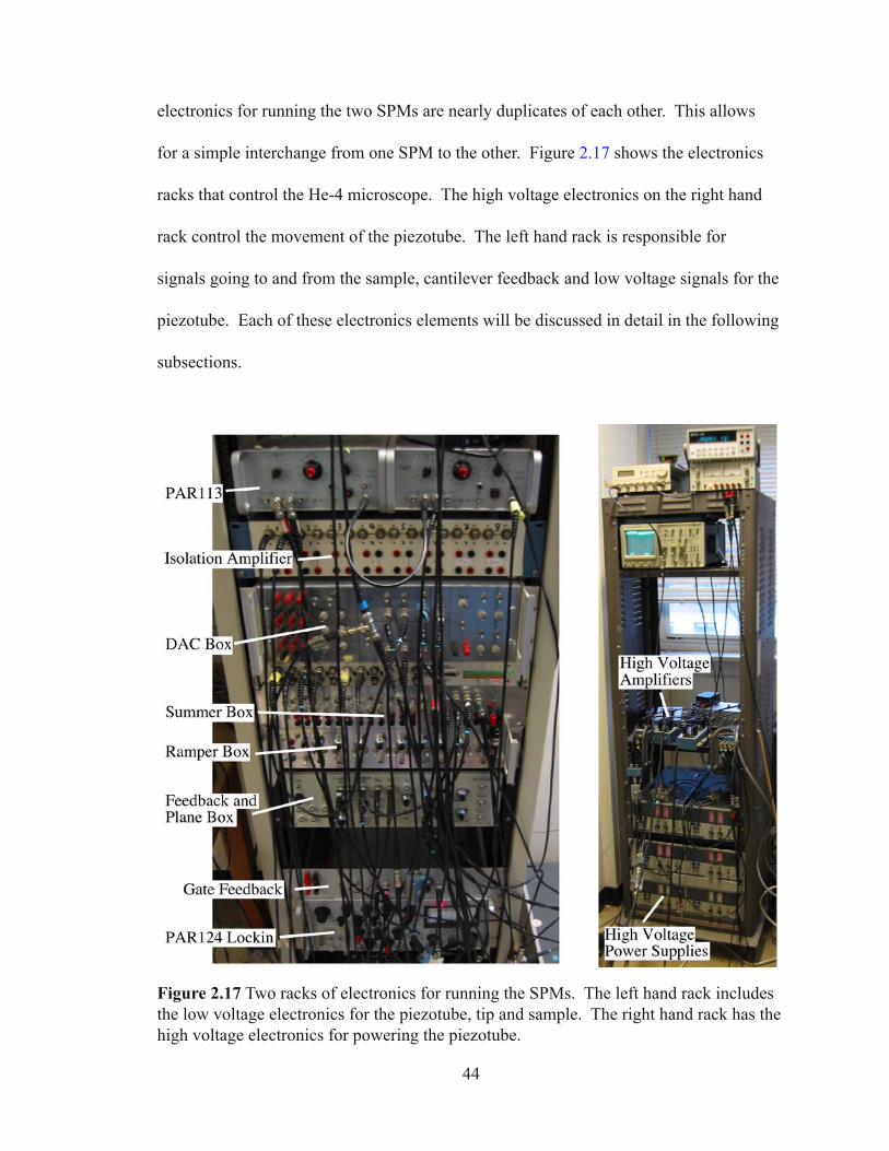
for a simple interchange from one SPM to the other. Figure 2.17 shows the electronics
racks that control the He-4 microscope. The high voltage electronics on the right hand
rack control the movement of the piezotube. The left hand rack is responsible for
signals going to and from the sample, cantilever feedback and low voltage signals for the
piezotube. Each of these electronics elements will be discussed in detail in the following
subsections.
Figure 2.17 Two racks of electronics for running the SPMs. The left hand rack includes the low voltage electronics for the piezotube, tip and sample. The right hand rack has the high voltage electronics for powering the piezotube.

45
2.4.1. Digital to Analog Convertor Box
This is the main box for controlling the experiment via the computer. It is
responsible for the x,y and z movement of the tip and the voltages on the gates and tip.
It is programmed by a PCI digital output board made by National Instruments16. This
board is capable of outputting 32 digital signals of which we use 22 for the control of
the experiment. The lab now has two versions of this converter box. The old one is
capable of outputting eight analog channels, is run off of batteries and is layed out on a
homemade circuit board. The new box is capable of outputting 16 channels, runs off of
two DC power supplies and was built on a professional printed circuit board.
Figure 2.18 sketches the main circuit diagram showing the isolation and
conversion circuits. The digital signals go from the computer to the DAC box and
then inside the box each of the lines goes through a digital isolator chip, (Burr-Brown
ISO15017) which isolates the ground of the computer from the ground of the box. These
chips capacitively couple the input to the output. This means that they are sensitive to
changes on the input level making them rather tricky to work with. It is necessary to
filter the input lines to remove any ringing on them due to the cable and to make sure that
the voltage does not swing outside of 0 to 5 volts. This filtering is accomplished by the
1000 Ohm resistors at the input of each chip, which act as low pass filters with the input
capacitance of the ISO150s. The 220 Ohm and 330 Ohm resistors ensure that the voltage
stays within the range 0 to 5 Volts. From the isolators the 16 data signals travel to the
AD669 analog to digital converter made by Analog Devices. These are 16bit converters
17 Burr-Brown (Texas Instruments) ISO-150
16 National Instruments, www.ni.com PCI-DIO-32HS

46
Fig
ure
2.18
Sch
emat
ic d
iagr
am o
f th
e D
AC
box
cir
cuit.
Eac
h in
put l
ine
goes
thro
ugh
the
ISO
150
as
show
n. T
hen
the
lines
go
to th
e co
nver
ters
, add
ress
dec
oder
and
con
trol
logi
c.

47
with a settling time of 8µs. They are double buffered with separate run (LDAC) and load
lines (L1 and CS) allowing the simultaneous updating of all the channels. This means
that we are able to update all the channels at 100kHz.
In order to achieve this fast update rate it is necessary to be able to selectively
load data into each chip. This is accomplished using four of the input lines as a binary
address, which is decoded by the 74HC154 chip. From this chip each of the decoded
lines runs to one of the load pins of the AD669. The last two input lines are used for
loading and running the AD669. The LDAC line goes through a one-shot, (74HC123)
which converts a transition from low to high to a pulse. The length of the pulse is
controlled by the resistor and capacitor on the one-shot. The last input is the L1 line,
which should load new data each time it transitions. To accomplish this it goes to two
one-shots, one creating a pulse on low to high transitions and the other on high to low.
These two pulse are passed through an and gate (74HC08) to get the resulting pulse each
time the input line transitions.
To better illustrate the timing of a load sequence Figure 2.19 shows three of
the lines. The blue trace is one of the data bits transitioning from low to high. A short
time later (caused by the time to decode) the red address line goes low. The green line
also goes to the AD669 chip and controls the transparency of the latch. When both the
red and green lines are low, the latch is transparent. When one of them goes high, the
data present at that time is latched. The length of time that the green line stays low is
controlled by the one-shot (74HC123). So the data present when the green line goes
high is loaded into the converter. Figure 2.20 shows the entire sequence of loading
three values of data followed by a conversion. The chip that we are looking at has data

48
loaded when the red line is low. The other two times the green line goes low, data is
being loaded into two other converters. The black line going high is the signal to start a
Figure 2.20 Shows the timing for a sequence of conversions by the DAC box. Each time the load buffer (green) goes low data is loaded into one of the chips based on which of the address lines (red) is also low. The data bit (blue) line shows a representative line of data. After loading all of the desired chips, the Load DAC (black) line goes high signaling the start of a conversion for all of the chips. The analog data is ready at the output 8µs later.
Figure 2.19 The timing of the loading of data into the AD669 chip. Data is latched in the buffer of the AD669 when either the address (red) or load buffer (green) line goes high. At that time the data bit (blue) is latched in the buffer and a new chip can be loaded. The length of time that the load buffer line stays low is set by a one-shot chip to be much shorter than the time between outputs from the computer.

49
conversion on all of the DACs in the box, and their data is ready at the output 8µs later.
The analog output of the AD669 chips goes through a low pass filter to remove
any of the digital noise that may be on it. Then the signal goes to the front panel where
it can go to the gates, tip, piezotube and other electronics. The 16-bit outputs give a
minimum step size of 0.3 mV. When this is divided down further like on the gates an
even higher resolution can be obtained. On the piezotube this gives a step size of around
0.25 nm depending on the total scan range of the tube.
2.4.2. Surface Flattening Box
The second electronics box processes the x, y voltages from the DAC box to
create the movements of the tip. This box receives as inputs the x and y values from
the DAC box. It turns these two inputs into both a positive and negative output, which
will go to the piezotube after being further amplified. This is necessary since opposite
quadrants of the tube receive opposite voltages to increase the scan area. It also uses
these two inputs to output a plane, which can correct for any tilt in the sample. The slope
of the plane is controlled by the two potentiometers on the right hand side of the box.
Figure 2.21 shows the schematic of the circuit. The input first goes through a differential
amplifier followed by an optional low pass filter. At this point the positive output goes to
the front panel and the negative output goes through an inverting amplifier. To produce
the slope of the plane, a potentiometer is used to create a variable gain negative signal
that is summed with the positive output. The potentiometer allows the signal to go from
–3 to 0 times the positive signal giving slopes in the range of –1.5 to +1.5. This is done

50
Fig
ure
2.21
Sch
emat
ic o
f th
e ci
rcui
t use
d to
fit a
pla
ne to
the
surf
ace.
The
X a
nd Y
vol
tage
fro
m th
e co
mpu
ter
are
inpu
t. T
he
user
can
adj
ust t
he s
lope
in b
oth
dire
ctio
ns b
y us
ing
the
pote
ntio
met
ers.
A Z
off
set m
ay a
lso
be a
dded
.
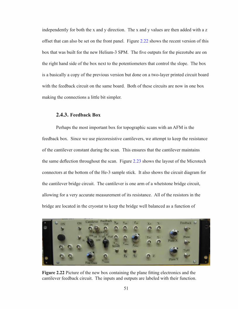
51
independently for both the x and y direction. The x and y values are then added with a z
offset that can also be set on the front panel. Figure 2.22 shows the recent version of this
box that was built for the new Helium-3 SPM. The five outputs for the piezotube are on
the right hand side of the box next to the potentiometers that control the slope. The box
is a basically a copy of the previous version but done on a two-layer printed circuit board
with the feedback circuit on the same board. Both of these circuits are now in one box
making the connections a little bit simpler.
2.4.3. Feedback Box
Perhaps the most important box for topographic scans with an AFM is the
feedback box. Since we use piezoresistive cantilevers, we attempt to keep the resistance
of the cantilever constant during the scan. This ensures that the cantilever maintains
the same deflection throughout the scan. Figure 2.23 shows the layout of the Microtech
connectors at the bottom of the He-3 sample stick. It also shows the circuit diagram for
the cantilever bridge circuit. The cantilever is one arm of a whetstone bridge circuit,
allowing for a very accurate measurement of its resistance. All of the resistors in the
bridge are located in the cryostat to keep the bridge well balanced as a function of
Figure 2.22 Picture of the new box containing the plane fitting electronics and the cantilever feedback circuit. The inputs and outputs are labeled with their function.
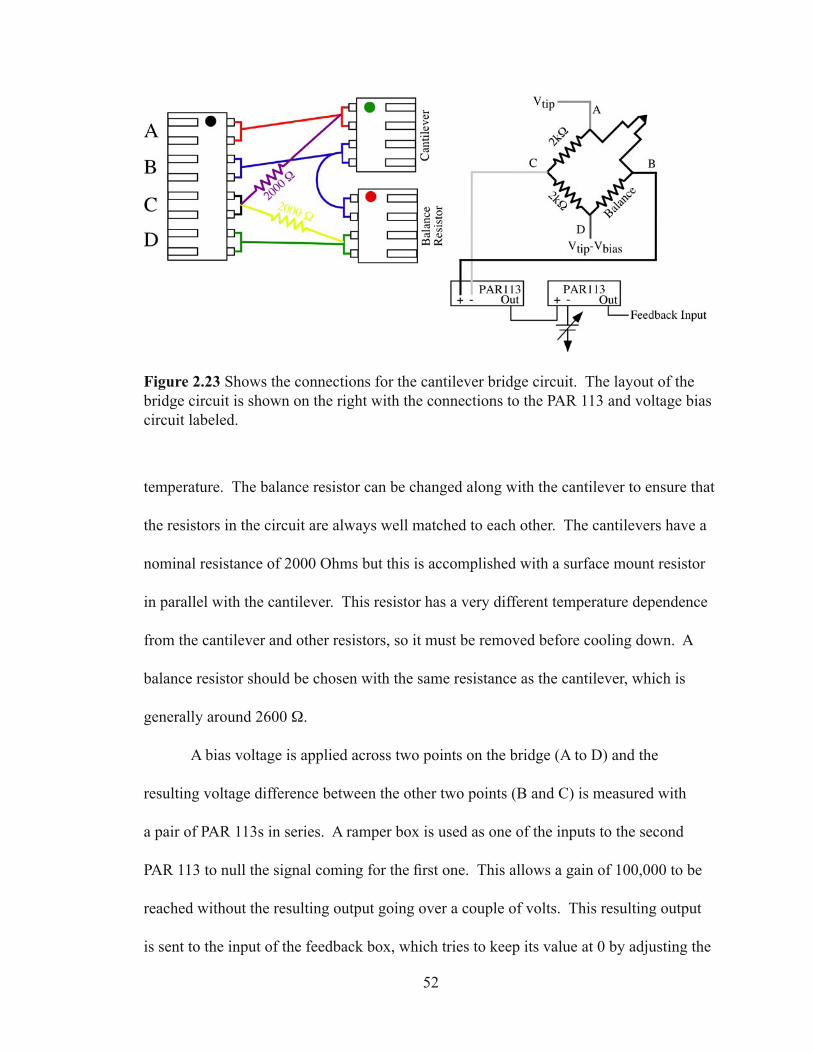
52
temperature. The balance resistor can be changed along with the cantilever to ensure that
the resistors in the circuit are always well matched to each other. The cantilevers have a
nominal resistance of 2000 Ohms but this is accomplished with a surface mount resistor
in parallel with the cantilever. This resistor has a very different temperature dependence
from the cantilever and other resistors, so it must be removed before cooling down. A
balance resistor should be chosen with the same resistance as the cantilever, which is
generally around 2600 Ω.
A bias voltage is applied across two points on the bridge (A to D) and the
resulting voltage difference between the other two points (B and C) is measured with
a pair of PAR 113s in series. A ramper box is used as one of the inputs to the second
PAR 113 to null the signal coming for the first one. This allows a gain of 100,000 to be
reached without the resulting output going over a couple of volts. This resulting output
is sent to the input of the feedback box, which tries to keep its value at 0 by adjusting the
Figure 2.23 Shows the connections for the cantilever bridge circuit. The layout of the bridge circuit is shown on the right with the connections to the PAR 113 and voltage bias circuit labeled.
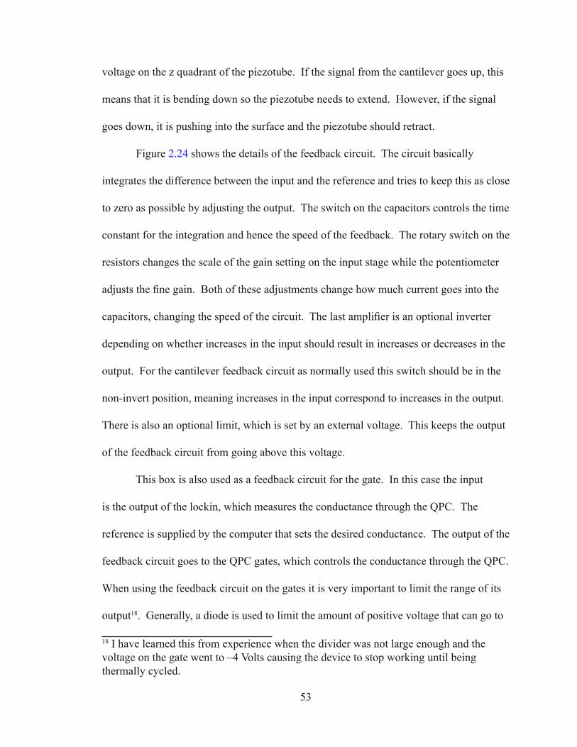
53
voltage on the z quadrant of the piezotube. If the signal from the cantilever goes up, this
means that it is bending down so the piezotube needs to extend. However, if the signal
goes down, it is pushing into the surface and the piezotube should retract.
Figure 2.24 shows the details of the feedback circuit. The circuit basically
integrates the difference between the input and the reference and tries to keep this as close
to zero as possible by adjusting the output. The switch on the capacitors controls the time
constant for the integration and hence the speed of the feedback. The rotary switch on the
resistors changes the scale of the gain setting on the input stage while the potentiometer
adjusts the fine gain. Both of these adjustments change how much current goes into the
capacitors, changing the speed of the circuit. The last amplifier is an optional inverter
depending on whether increases in the input should result in increases or decreases in the
output. For the cantilever feedback circuit as normally used this switch should be in the
non-invert position, meaning increases in the input correspond to increases in the output.
There is also an optional limit, which is set by an external voltage. This keeps the output
of the feedback circuit from going above this voltage.
This box is also used as a feedback circuit for the gate. In this case the input
is the output of the lockin, which measures the conductance through the QPC. The
reference is supplied by the computer that sets the desired conductance. The output of the
feedback circuit goes to the QPC gates, which controls the conductance through the QPC.
When using the feedback circuit on the gates it is very important to limit the range of its
output18. Generally, a diode is used to limit the amount of positive voltage that can go to
18 I have learned this from experience when the divider was not large enough and the voltage on the gate went to –4 Volts causing the device to stop working until being thermally cycled.

54
Fig
ure
2.24
Sch
emat
ic o
f th
e fe
edba
ck c
ircu
it. T
he in
put i
s th
e si
gnal
to f
eedb
ack
on w
hile
the
outp
ut is
the
sign
al th
at is
ad
just
ed.
The
ref
eren
ce s
ets
the
valu
e th
at th
e in
put s
houl
d eq
ual.
The
lim
it m
ay b
e us
ed to
pre
vent
the
feed
back
fro
m g
oing
po
sitiv
e.
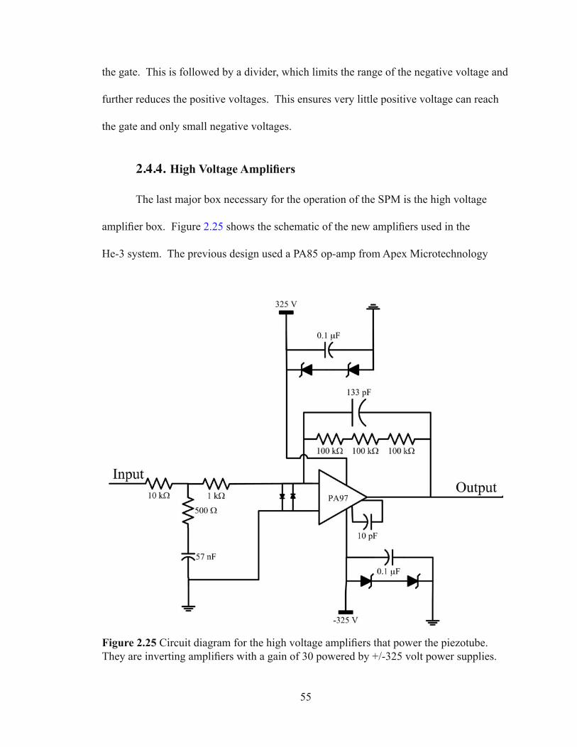
55
the gate. This is followed by a divider, which limits the range of the negative voltage and
further reduces the positive voltages. This ensures very little positive voltage can reach
the gate and only small negative voltages.
2.4.4. High Voltage Amplifiers
The last major box necessary for the operation of the SPM is the high voltage
amplifier box. Figure 2.25 shows the schematic of the new amplifiers used in the
He-3 system. The previous design used a PA85 op-amp from Apex Microtechnology
Figure 2.25 Circuit diagram for the high voltage amplifiers that power the piezotube. They are inverting amplifiers with a gain of 30 powered by +/-325 volt power supplies.

56
and is described in Mark Eriksson and Mark Topinka’s theses [Eriksson, (1997);
Topinka, (2002)]. We have decided to use a different op-amp in our design to achieve a
higher scan range. We have used the PA97, which is capable of outputting more voltage
but less current. Since we are just driving the piezotube, which is a capacitive load this
is not a problem in our application. The box contains five identical circuits for the +X,
-X, +Y, -Y and Z quadrants of the piezotube. The op-amp is in an inverting amplifier
configuration with a gain of 30 giving an output range of +/- 300 Volts when driven by
the DAC box, which outputs +/- 10 Volts. The diodes on the power lines are to protect
the op-amp from spikes in the power, which may damage them. The diodes on the
inputs keep them close together so that the output will not be too large. There is a 10 pF
capacitor on two pins of the op-amp that is necessary for stability when the gain is greater
than 10.
2.4.5. Other Electronics
During the course of my research, I have built a couple of other boxes that we
routinely use with the SPM. I will briefly describe them here but their circuits are rather
straight forward so I will not go into much detail. The first box is what around lab is
known as a “Ramper Box.” This box was designed by Jordan Katine and has been in
use in our lab for many years [Katine, (1996)]. It consists of one output that ramps as a
function of time and eight outputs that are constant. The speed of the ramp is selected
using a switch on the front along with a potentiometer. The voltage for the fixed outputs
is determined in the same way. The complete circuit diagrams are in Jordan’s thesis.
The second box is a differential summer box. It sums the inputs from up to four

57
channels and puts them on the output. We mostly use this box to add voltages from
different sources together before going to the gates, ohmics or tip. Figure 2.26 shows
the circuit schematic. Each input goes through a differential amplifier and then into the
summing amplifier. After they are all summed together, the output goes to the front panel
of the box. The entire circuit is run off of two 1.2 Amp Hour 12V lead-acid batteries19
that are enclosed in the box. The box with the summer circuit has two copies of it run off
of separate sets of batteries allowing the summation of two different voltages. The use of
the OP97 op-amps in the circuit gives excellent noise performance with very little power
use. I have to recharge the batteries less than once a week even with daily use of the
circuits.
Figure 2.26 Schematic diagram of the summing circuit used in the summer box. There are four differential inputs of which one is shown which then all are summed together at the second op-amp. The output comes out at Vout.
19 PowerSonic model PS-1212

58
2.4.6. Computer
All of the control and data acquisition is controlled by a Macintosh computer
through two National Instruments PCI cards. As mentioned previously, a digital output
card controls the signals going to the SPM. The input back to the computer is through a
PCI-MIO-16XE-10 board, which has 8 channels of 16-bit differential input. The board is
capable of sampling the input at 100kHz. The interface with the boards is handled by the
data acquisition program, AFM Program, originally written by Mark Topinka that I have
modified to handle the updated boards that we are now using20.
Figure 2.27 shows a screen shot of the data acquisition program. The program
consists of four windows: dashboard, sweep, script, and console. The console window
provides basic feedback to the user about problems that have occurred and other
diagnostic information. The script is the main window for user input. The user enters
commands into the script window to control everything from the movement of the tip,
to the gate voltages and data analysis functions. Appendix B details all of the script
commands available in the program, which now totals over 400. The sweep window is
for acquiring and displaying one-dimensional data sets. The sweep window is mainly
used for initial testing of a new device. For example, we use it to take traces of the
conductance versus gate voltage for the QPCs. It is also used for doing data analysis
when taking 1-D slices of images. The last and most complicated window of the program
20 National Instruments no longer seems to support accessing the PCI Macintosh boards through C function calls. They only support Labview but I was able to find an engineer who was willing to give me the drivers for the boards. The commands are the same as used by the PC boards if you ever need help in using them just look up the PC documentation.

59
Fig
ure
2.27
Scr
eens
hot o
f th
e A
FM p
rogr
am s
how
ing
the
four
win
dow
s: d
ashb
oard
, sw
eep,
scr
ipt a
nd c
onso
le.
60
is the dashboard. It has up to four graphs showing different scans. It also has readouts of
all the variables associated with the operation of the SPM. These range from the distance
off the surface, the voltages on the gates, the working directory, etc. At the bottom of the
window, all of the input and output values are displayed. The blue cursor in the graphs
shows the current position of the tip and can be moved with the mouse. The red and
green cursors define the corners of the current scan area.
One of the recent major changes to the program was to go from 12-bit analog
outputs to 16-bit ones. This reduced the minimum step size for the tip from about 4 nm
down to 0.25 nm. It also reduced the voltage steps on the gates from about 5 mV to
0.3mV. This was accomplished by using the new DAC box, which has 16-bit converters
in it instead of an old National Instruments card. In order to do this the format of the
output data had to be changed. The sequence of data to output an analog signal is now
as follows. Send the data to the DAC box for each channel that is going to be changed.
Then send the convert signal to all of the DACs. Repeat this process for each output.
There is a minimum of three sets of data that must be sent for each conversion. This is
due to the timing function of the board, so if fewer channels than this are being updated
just repeat the data for one of them. All of the information is sent to the DAC box as
16-bit integers from an array, two elements of which are sent at each output to create the
32-bit word. The first 16-bits are the data. The second 16-bits are more complicated and
are formatted as follows: lowest 4 bits are not used, next 4 bits are the address, next bit is
unused, next is the chip select and last is the start conversion.
There are two other versions of the program, one is the data analysis version,
which has all of the communication with the PCI boards removed and has larger graphs

61
for a better display of the data. We use this version to look at and analyze all of the data
after acquiring it. The third version of the program is used by the people in our group
working on quantum dots. It interfaces with a 20-bit digital to analog converter through
the serial port. This gives a much finer control of the gate voltages but greatly limits the
speed of data acquisition making it impractical for the SPM.
62
Chapter 3
Imaging Techniques
This chapter covers the different imaging techniques that we use to look at
coherent electron flow. To find the location of our device we use standard contact
topographic imaging while we use scanning gate microscopy techniques for acquiring
images of electron flow. Section 3.1 describes the procedures that we use at room
temperature to align the tip so that it is over the device at liquid helium temperature.
Section 3.2 discusses the procedures that are done before an image of electron
flow can be obtained, these include finding the device and making sure the surface is flat.
The remaining three sections of the chapter discuss techniques that we have developed
to image electron flow. These techniques allow the study of different properties of the
electron flow in the two-dimensional electron gas.
The first and simplest one is discussed in section 3.3 where we put a fixed
voltage on the tip and scatter the electrons. By measuring the change in conductance as
a function of tip position, an image of the electron flow is obtained. This technique is
used to image the electron flow through the two-dimensional electron gas and to spatially
profile the local electron density.
Section 3.4 outlines the second method, which is an extension of this method
where we oscillate the voltage on the tip and lockin to the signal that varies at this
frequency. This gives an image of the derivative of electron flow with respect to
the tip position. This is very useful when studying the interference fringes oriented
63
perpendicular to the electron flow.
In section 3.5 we discuss our third method that involves ramping the voltage on
the tip to look at the local density of states under it. This is similar to STM spectroscopy
measurements of differential conductance versus tip voltage, which measure the local
density of states as a function of energy.
3.1. SPM Operation – Room Temperature Alignment
The section describes the procedure used to align the scanning probe microscope
(SPM) at room temperature so that the tip will be able to reach the device at liquid
helium temperature. When the SPM cools, the position of the tip drifts relative to the
sample. This drift is caused by several factors including the differential contraction of
the piezotube and brass cage, the tilt of the SPM head and small cracks in the piezotube.
The drift is fairly repeatable as long as nothing is changed with the SPM. When the SPM
is cold the scan range of the piezotube shrinks by about a factor of 4 giving a total scan
range of around 15x15 µm at 4.2 K. The limited scan range and drift means that the
starting position of the tip has to be carefully chosen at room temperature to ensure it is
within reach of the device at 4.2 K. To facilitate the positioning of the tip, each sample
has an alignment grid written on it at the same time as the gates.
Figure 3.1 shows a topographic image of two –1’s in the alignment grid, which
are patterned by electron-beam lithography and thin-film deposition. The grid consists
of two numbers at each point, which represent the x and y coordinate in units of 10 µm.
The top left number is the y-coordinate and the bottom right one is the x-coordinate.
The device is located at (0,0), so that the two numbers give the distance away from the
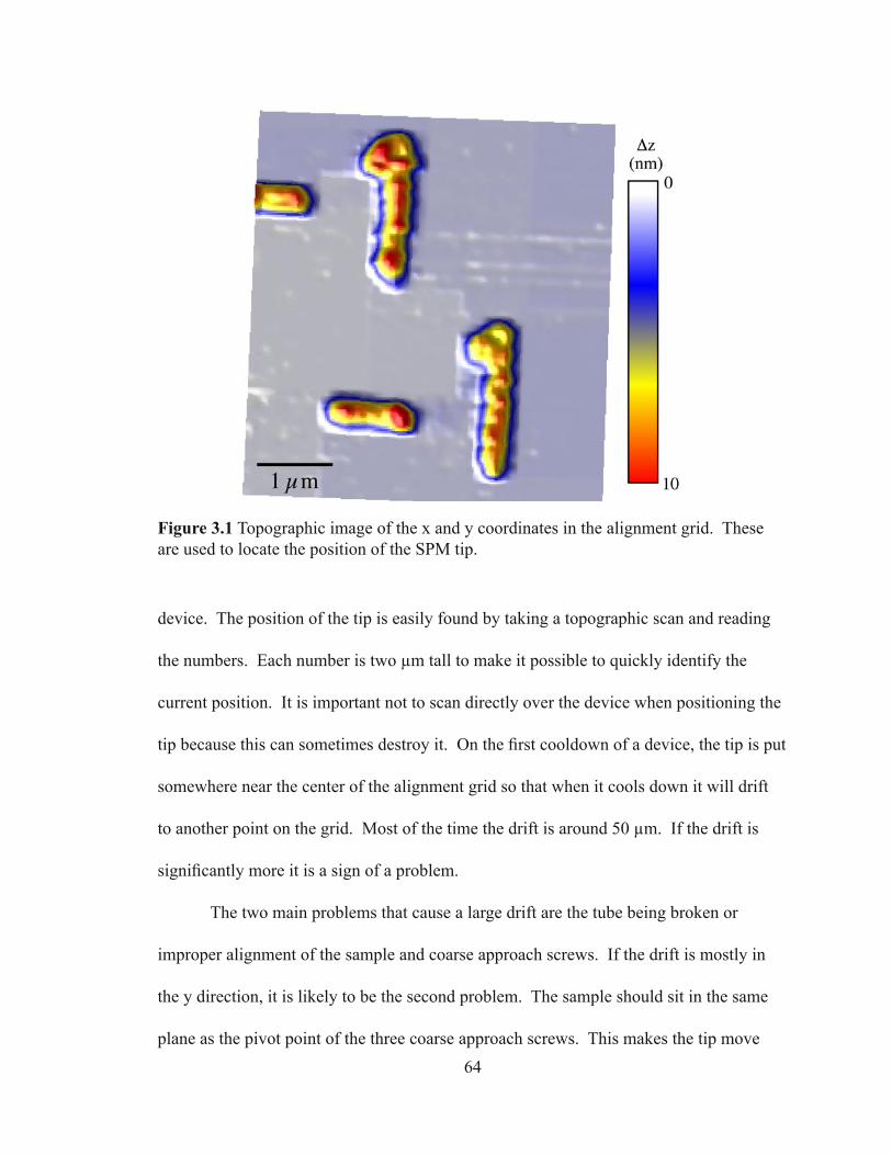
64
device. The position of the tip is easily found by taking a topographic scan and reading
the numbers. Each number is two µm tall to make it possible to quickly identify the
current position. It is important not to scan directly over the device when positioning the
tip because this can sometimes destroy it. On the first cooldown of a device, the tip is put
somewhere near the center of the alignment grid so that when it cools down it will drift
to another point on the grid. Most of the time the drift is around 50 µm. If the drift is
significantly more it is a sign of a problem.
The two main problems that cause a large drift are the tube being broken or
improper alignment of the sample and coarse approach screws. If the drift is mostly in
the y direction, it is likely to be the second problem. The sample should sit in the same
plane as the pivot point of the three coarse approach screws. This makes the tip move
Figure 3.1 Topographic image of the x and y coordinates in the alignment grid. These are used to locate the position of the SPM tip.
65
straight away from the sample when the screw is turned as opposed to moving in the y
direction. When the SPM is cooled, there is a differential contraction between the brass
cage and the piezotube. This requires that the tip be pulled off the surface by about
0.6 mm (2 turns of the coarse approach screw) so that it does not hit the surface upon
cooling. If the height of the sample with respect to the coarse approach screw is incorrect
this leads to a large movement in the y direction. The second problem is a broken tube,
which can usually be identified by a large hysteresis at room temperature. The first few
lines in a topographic image will have a different slope than the rest of the scan.
When the SPM has cooled to liquid helium temperature, it is necessary to find the
location of the tip. If it is not within reach of the device, the drift is calculated and this
is used as the starting position for a second cooldown. After warming up, the position
of the tip is adjusted by turning the x and y coarse position screws. The location of
the tip must be adjusted so that it is correct when the cryostat is upside down since this
is the orientation when it is cold. This can be done by flipping the cryostat over after
each movement of the tip and finding the new location. Another method is to note the
change in position when you flip the cryostat and use this to adjust the desired location.
The location should not move more than around 5 µm when the cryostat is flipped over.
After the tip is positioned, the SPM is cooled back down and the location of the device is
checked to see if it is within reach. I have always had the device be within reach on the
second cooldown as the drift is fairly repeatable. The biggest factor in the drift seems to
be the piezotube because the drift is fairly constant from sample to sample and tip to tip
unless the piezotube is changed.
66
3.2. SPM Operation – Liquid Helium Temperature
This section describes the steps necessary to acquire images of electron flow
once the dewar and SPM have been cooled to 4.2 K. The first step is to approach the
surface using the coarse approach rod. With the cantilever feedback on, the coarse
approach screw is turned until the voltage on the Z quadrant of the piezotube needed to
reach the surface is about 100 V. This allows a decent scan range and the flexibility to
adjust the height based on the location of the device. Topographic scans are taken to
determine the location of the device. Taking topographic scans can change the ionization
of the donor atoms underneath the tip by straining the sample or inducing charge on the
atoms. Therefore it is not a good idea to take topographic scans to close to the device
because of the risk of changing its electrical properties. If the tip cannot reach the
device, extra voltage can be added to some of the quadrants of the piezotube to extend
the scan range. An extra 200 V can be safely added, which doubles the scan range. If
the device can be reached, initial checks of the device properties are performed. If it is a
QPC the following checks are performed, that the ohmics work, the gates work and that
conductance plateaus are visible.
Assuming that everything is working so far, the flattening of the surface is
adjusted. The surface flattening box discussed in Section 2.4.2 adjusts the height of the
tip as a function of position so that the feedback does not have to work as hard to keep
the tip on the surface. It also allows scans with the feedback off and the tip a fixed height
above the surface. The plane is adjusted in a small area away from any gates or objects
on the surface. Repeated topographic scans are taken and the potentiometers on the plane
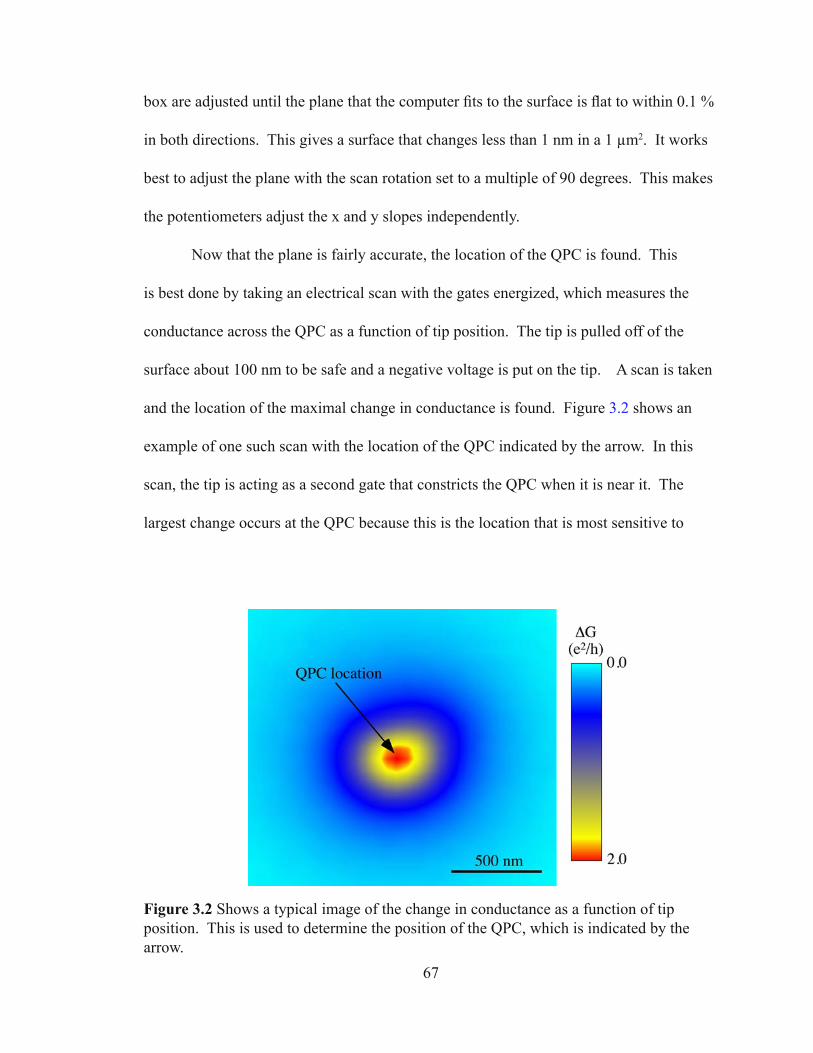
67
box are adjusted until the plane that the computer fits to the surface is flat to within 0.1 %
in both directions. This gives a surface that changes less than 1 nm in a 1 µm2. It works
best to adjust the plane with the scan rotation set to a multiple of 90 degrees. This makes
the potentiometers adjust the x and y slopes independently.
Now that the plane is fairly accurate, the location of the QPC is found. This
is best done by taking an electrical scan with the gates energized, which measures the
conductance across the QPC as a function of tip position. The tip is pulled off of the
surface about 100 nm to be safe and a negative voltage is put on the tip. A scan is taken
and the location of the maximal change in conductance is found. Figure 3.2 shows an
example of one such scan with the location of the QPC indicated by the arrow. In this
scan, the tip is acting as a second gate that constricts the QPC when it is near it. The
largest change occurs at the QPC because this is the location that is most sensitive to
Figure 3.2 Shows a typical image of the change in conductance as a function of tip position. This is used to determine the position of the QPC, which is indicated by the arrow.

68
charge. This process is repeated after zooming in on this area to pinpoint the location of
the QPC.
Depending on how complicated the device is, an image of the gates may be
obtained. This should be done without touching the surface because that can disturb the
donor atoms. The feedback circuit has been modified to allow this type of scan. There
is an input marked limit, which limits the positive range of the output. When a voltage is
attached here, the output is clamped by a diode so that it cannot go more than 0.3 V above
this value. One of the outputs of the ramper box is attached to the limit and the voltage is
set so that the feedback cannot output a positive value. This keeps the tip from pushing
out but allows it to pull off the surface if it hits something. Scans are taken over the gate
area, reading the Z voltage and cantilever deflection. The tip is moved progressively
closer to the surface until an image of the gates appears. Figure 3.3 shows an example
of the resulting scan, which measures the cantilever deflection. There is no change in the
Figure 3.3 Image of the change on the cantilever voltage showing the location of the gates. This image was taken with the feedback limit enabled to keep the tip from hitting the surface of the GaAs.

69
deflection unless an object is sticking up from the surface and then the piezotube retracts.
Now that the location of the gates is known, a better fit to the surface is found.
This is accomplished with the script command “autoflatten”. The command takes
a series of points, finds the surface at each one and then fits a plane to the resulting
values. It finds the surface at each point by pushing into the surface many times with
progressively less force. It takes the average of all of the readings of the surface height
and this is the value for the height at that location. The autoflatten command has the
option of excluding some of the worst points from the fit. It is generally a good idea to
use this feature in case the routine does not get a good reading for some of the points on
the surface. The resulting plane is put in graph A, the left hand graph in the computer
program discussed in section 2.4.6. When the Z-guide is on, the values in the graph are
output to the Z quadrant of the piezotube as a function of position to keep the tip a fixed
distance from the surface. With the Z-guide on the accuracy of some of the points can
be checked by moving the tip and slowly approaching the surface. If they appear to be
good, the flattening is repeated with the Z-guide on to obtain a very accurate surface.
Generally, none of the points in the fit of the plane have an error greater than 1 nm over
a range of 25 µm2. Once this is finished, everything is ready to start taking images of
electron flow.
3.3. Scanned Gate Microscopy
This method of imaging electron flow uses the SPM tip as a moveable gate that
scatters electron waves. The tip backscatters some of the electron waves back through
the QPC reducing its conductance. When the tip is over an area of high electron flow,
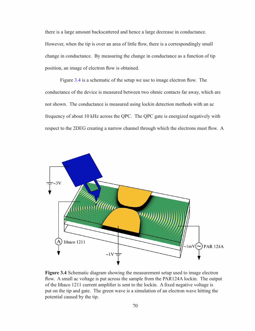
70
there is a large amount backscattered and hence a large decrease in conductance.
However, when the tip is over an area of little flow, there is a correspondingly small
change in conductance. By measuring the change in conductance as a function of tip
position, an image of electron flow is obtained.
Figure 3.4 is a schematic of the setup we use to image electron flow. The
conductance of the device is measured between two ohmic contacts far away, which are
not shown. The conductance is measured using lockin detection methods with an ac
frequency of about 10 kHz across the QPC. The QPC gate is energized negatively with
respect to the 2DEG creating a narrow channel through which the electrons must flow. A
Figure 3.4 Schematic diagram showing the measurement setup used to image electron flow. A small ac voltage is put across the sample from the PAR124A lockin. The output of the Ithaco 1211 current amplifier is sent to the lockin. A fixed negative voltage is put on the tip and gate. The green wave is a simulation of an electron wave hitting the potential caused by the tip.

71
negative voltage is put on the tip, which depletes the electrons below. Figure 3.5 shows
an example of an image of electron flow obtained with this technique at a temperature
of 1.7 K. The image shows the electron flow coming from a QPC off the right side of
the scan. The blue areas are areas of high electron flow while the black are areas of no
electron flow. The image is decorated by interference fringes throughout the scan area
showing that the flow is coherent.
The most important requirement for obtaining an image with this method is that
the voltage on the tip is sufficient to deplete the electron gas below. Figure 3.6 shows the
effect of making the voltage on the SPM tip more negative. In each successive image the
voltage on the tip changes by 0.5 V going from –1.5 V up to –4.0 V. There is no change
in conductance until the tip first depletes the electron gas and then the signal quickly
increases. There is no image of electron flow in Figure 3.6 (a and b) since the voltage
on the tip is too small. Once the tip is making a depletion region the image of electron
flow is obtained. In Figure 3.6 (d-f), there is little change in the image as a function of
tip voltage. In these images, the tip’s depletion region is growing but does not seem
Figure 3.5 Image of electron flow from a QPC located to the right of the scan at a temperature of 1.7 K. The flow is decorated by interference fringes throughout the entire scan area.
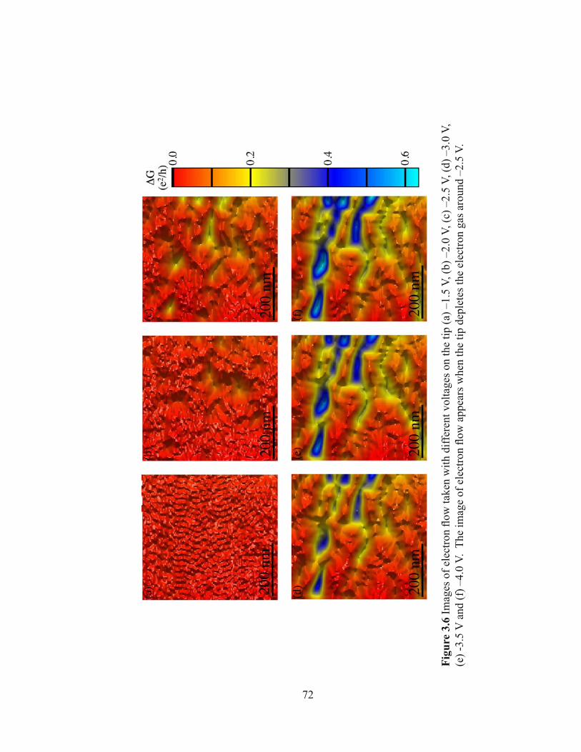
72
Fig
ure
3.6
Imag
es o
f el
ectr
on fl
ow ta
ken
with
dif
fere
nt v
olta
ges
on th
e tip
(a)
–1.
5 V
, (b)
–2.
0 V
, (c)
–2.
5 V
, (d)
–3.
0 V
, (e
) -3
.5 V
and
(f)
–4.
0 V
. T
he im
age
of e
lect
ron
flow
app
ears
whe
n th
e tip
dep
lete
s th
e el
ectr
on g
as a
roun
d –2
.5 V
.
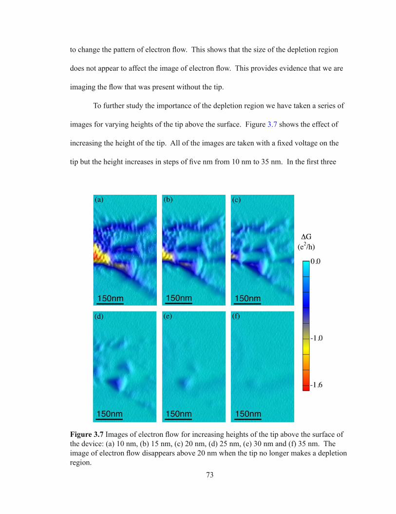
73
to change the pattern of electron flow. This shows that the size of the depletion region
does not appear to affect the image of electron flow. This provides evidence that we are
imaging the flow that was present without the tip.
To further study the importance of the depletion region we have taken a series of
images for varying heights of the tip above the surface. Figure 3.7 shows the effect of
increasing the height of the tip. All of the images are taken with a fixed voltage on the
tip but the height increases in steps of five nm from 10 nm to 35 nm. In the first three
Figure 3.7 Images of electron flow for increasing heights of the tip above the surface of the device: (a) 10 nm, (b) 15 nm, (c) 20 nm, (d) 25 nm, (e) 30 nm and (f) 35 nm. The image of electron flow disappears above 20 nm when the tip no longer makes a depletion region.

74
images, there is an image of electron flow. This is because the tip is close enough to the
surface to deplete the electron gas and backscatter electrons through the QPC. For the
last three images, there is almost no signal as a function of tip position. This is because
the voltage on the tip is not sufficient to deplete the 2DEG, leaving nothing to backscatter
the electrons.
We have modeled the effect of the tip on the 2DEG using a 3D Poisson simulator.
The details of the simulator can be found in the thesis of Mark Topinka [Topinka, (2002)].
For the simulation we modeled the tip as a sphere at the end of a cone. The angle of the
cone was taken to be 12 degrees as given in the specifications for our cantilevers. The
radius of the sphere used was 24 nm, which is a typical radius of the tips judging by
topographic images. In the simulation, we found the size of the depleted region under
the tip as a function of the distance of the tip from the surface. This shows that the tip
first depletes the electron gas when it is around 25 nm from the surface. Our images
of electron flow also start to appear when the tip is within 25 nm of the surface. This
provides another piece of evidence that the important factor in obtaining an image of
electron flow is creating a depletion region. A further confirmation of the necessity of the
depletion region comes from a quantum mechanical simulation that shows that the signal
increases rapidly when the tip first depletes the 2DEG [Shaw, (2002)].
Figure 3.8 illustrates why it is necessary to have a depletion region in order to
acquire images of electron flow. If the tip just creates a bump in the potential felt by the
electrons, it will not backscatter electrons as shown in Figure 3.8 (a). This is because
the electrons still have enough energy to go over the bump and therefore will not be
reflected but merely bent. However, if the voltage is increased so that the bump reaches

75
the height of the Fermi energy as in Figure 3.8 (b), there is a region of depleted electrons.
This area is classically forbidden for the electrons and electron waves impingent on it
will be backscattered. This will scatter some of the electrons back through the QPC,
which reduces its conductance. Since the measurement is only sensitive to changes in
conductance this produces an image of electron flow, while the first case does not give
any signal.
The depletion region is also important for the high resolution of our technique.
Since the 2DEG is located 57 nm below the surface and the tip is at least a few nm above
the surface, the distance from the tip to the 2DEG is at least 60 nm. This distance sets the
half width of the perturbation from the tip in the 2DEG. However, we are easily able to
resolve features that are much smaller than this size. Figure 3.9 illustrates how this high
spatial resolution is achieved from the large depletion region below the tip. The tip acts
as a hard wall scatterer meaning that the angle of incidence of a wave is the same as the
angle of reflection. Therefore only an electron wave that hits normal to the tip will be
directly backscattered. All the other angles will be scattered but eventually make it to the
Figure 3.8 Diagram showing the importance of creating a depletion region under the tip. In (a) there is only a small bump and the electron is merely bent by the perturbation. In (b) the electron gas is depleted causing the electron to be backscattered by the potential.

76
ohmic. The red path that is directly backscattered can return back through the QPC and
reduce its conductance. This small part of the depletion region that backscatters electrons
is also important in producing the interference fringes perpendicular to the electron
flow that decorate the images. This will be discussed in more detail in Chapter 7. The
small spot on the tip that backscatters electrons to the QPC determines the resolution as
opposed to the entire width of the perturbation. This gives a much higher resolution than
would be initially expected.
3.4. Differential Imaging
The first method of imaging provides detail about the overall electron flow pattern
but it does not give information about changes in the flow. Because the signal comes
from one spot, we can use this to obtain a spatial derivative of electron flow by changing
the location of this spot. We have developed a second technique that provides an image
Figure 3.9 Diagram showing how the high spatial resolution is obtained. There are many paths of electrons hitting the tip but only the red path is backscattered through the QPC reducing its conductance. This is the path that hits the tip directly.
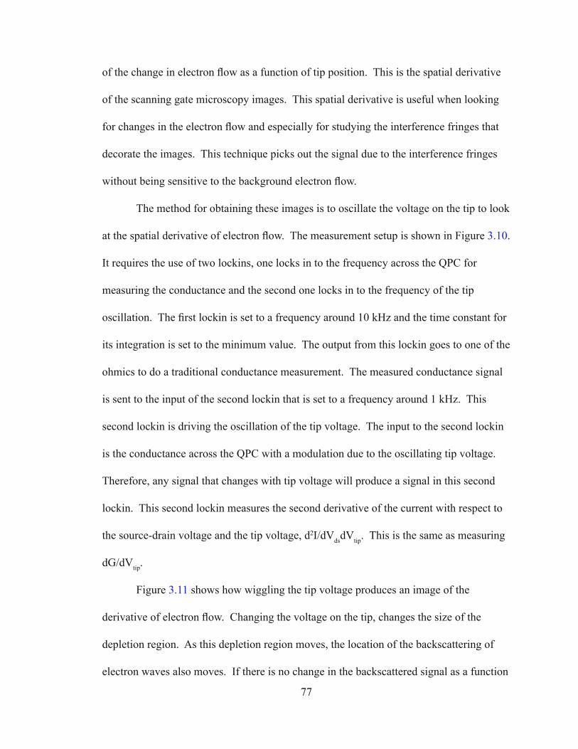
77
of the change in electron flow as a function of tip position. This is the spatial derivative
of the scanning gate microscopy images. This spatial derivative is useful when looking
for changes in the electron flow and especially for studying the interference fringes that
decorate the images. This technique picks out the signal due to the interference fringes
without being sensitive to the background electron flow.
The method for obtaining these images is to oscillate the voltage on the tip to look
at the spatial derivative of electron flow. The measurement setup is shown in Figure 3.10.
It requires the use of two lockins, one locks in to the frequency across the QPC for
measuring the conductance and the second one locks in to the frequency of the tip
oscillation. The first lockin is set to a frequency around 10 kHz and the time constant for
its integration is set to the minimum value. The output from this lockin goes to one of the
ohmics to do a traditional conductance measurement. The measured conductance signal
is sent to the input of the second lockin that is set to a frequency around 1 kHz. This
second lockin is driving the oscillation of the tip voltage. The input to the second lockin
is the conductance across the QPC with a modulation due to the oscillating tip voltage.
Therefore, any signal that changes with tip voltage will produce a signal in this second
lockin. This second lockin measures the second derivative of the current with respect to
the source-drain voltage and the tip voltage, d2I/dVds
dVtip
. This is the same as measuring
dG/dVtip
.
Figure 3.11 shows how wiggling the tip voltage produces an image of the
derivative of electron flow. Changing the voltage on the tip, changes the size of the
depletion region. As this depletion region moves, the location of the backscattering of
electron waves also moves. If there is no change in the backscattered signal as a function

78
of position, the size of the depletion region will not effect the measurement. In this case,
there is no signal on the second lockin because the derivative is zero. However, if the
signal changes as a function of position this will show up as a modulation in the signal
and the lockin will detect it giving rise to a signal. So the measurement of dG/dVtip
at a
fixed tip voltage gives an image of the derivative of electron flow.
Figure 3.10 Diagram showing the connections necessary for imaging the derivative of electron flow. There are two ac voltages, one across the QPC the other on the tip. The current through the QPC is input into the first PAR124A to get the conductance across the device. This is then sent to the second lockin, which measures the differential conductance with respect to the tip voltage.

79
An example of an image acquired with this technique is shown in Figure 3.12.
Figure 3.12 (a) is an image of the change in conductance using the scanning gate
microscopy technique. Figure 3.12 (b) shows an image of the derivative of electron flow
acquired at the same time by oscillating the tip voltage and measuring dG/dVtip
. Notice
that the interference fringes are much more pronounced in the derivative image, since
the slow varying background is removed. The fringes are now clearly visible at the top
of the image where they were hardly visible in the first image. This method of imaging
Figure 3.12 Two images of electron flow from the same area. (a) Image acquired with a fixed voltage on the tip. (b) Image acquired by locking into an ac voltage on the tip, giving the derivative in the direction of electron flow of the image in (a).
Figure 3.11 Schematic showing how the differential imaging technique works. As the voltage on the tip oscillates, the position of backscattering changes. By locking into this oscillation, only a signal that changes as a function of position is imaged.
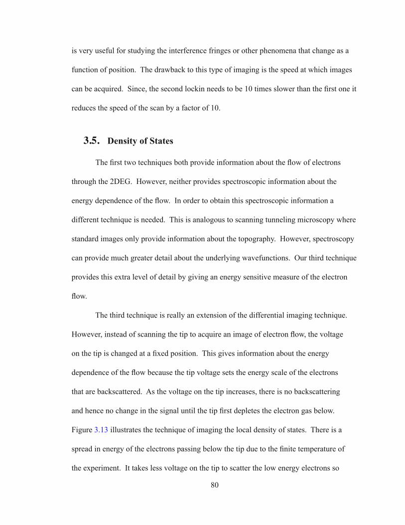
80
is very useful for studying the interference fringes or other phenomena that change as a
function of position. The drawback to this type of imaging is the speed at which images
can be acquired. Since, the second lockin needs to be 10 times slower than the first one it
reduces the speed of the scan by a factor of 10.
3.5. Density of States
The first two techniques both provide information about the flow of electrons
through the 2DEG. However, neither provides spectroscopic information about the
energy dependence of the flow. In order to obtain this spectroscopic information a
different technique is needed. This is analogous to scanning tunneling microscopy where
standard images only provide information about the topography. However, spectroscopy
can provide much greater detail about the underlying wavefunctions. Our third technique
provides this extra level of detail by giving an energy sensitive measure of the electron
flow.
The third technique is really an extension of the differential imaging technique.
However, instead of scanning the tip to acquire an image of electron flow, the voltage
on the tip is changed at a fixed position. This gives information about the energy
dependence of the flow because the tip voltage sets the energy scale of the electrons
that are backscattered. As the voltage on the tip increases, there is no backscattering
and hence no change in the signal until the tip first depletes the electron gas below.
Figure 3.13 illustrates the technique of imaging the local density of states. There is a
spread in energy of the electrons passing below the tip due to the finite temperature of
the experiment. It takes less voltage on the tip to scatter the low energy electrons so

81
they give a signal at the lowest voltage. As the voltage on the tip increases more of the
electron distribution is scattered until the 2DEG is fully depleted under the tip. When
the voltage on the tip is well above or below the Fermi energy there is little change in
the number of electrons backscattered as a function of tip voltage. However, when the
tip voltage is at the Fermi energy there is the largest change in the number of electrons
backscattered with tip voltage. This measurement gives a signal that is proportional to
the derivative of the electron energy distribution with respect to energy.
Figure 3.14 plots the differential conductance with respect to tip voltage,
dG/dVtip versus the tip voltage. There is very little signal until the tip first depletes
the electron gas around 2.5 V, then the signal rapidly rises and falls. This peak is in the
shape of the electron energy distribution as shown by the red line, which is the expected
Fermi distribution. There are two free parameters in this fit, the first one is the height of
the signal and the second one is the location of the maximum. The height of the peak
is an indication of the strength of the flow at the given point. The location of the peak
gives the local Fermi energy. The wiggles in the signal for larger tip voltages are due to
the size of the depletion region growing. The position of the front edge of the depletion
Figure 3.13 Schematic diagram showing how the density of states imaging technique works. As the voltage on the tip increases the backscattering of only certain energy electrons changes giving rise to a signal proportional to the local density of states.
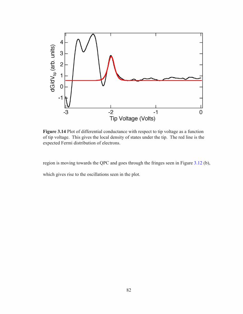
82
region is moving towards the QPC and goes through the fringes seen in Figure 3.12 (b),
which gives rise to the oscillations seen in the plot.
Figure 3.14 Plot of differential conductance with respect to tip voltage as a function of tip voltage. This gives the local density of states under the tip. The red line is the expected Fermi distribution of electrons.

83
Chapter 4
Imaging Local Electron Density
This chapter describes the results of our experiments to image local electron
density. Section 4.1 describes the sample structure and basic device properties including
the effect of the back gate on the electron density. Section 4.2 discusses the imaging
technique and presents images of coherent electron flow for different back gate voltages.
Section 4.3 details the data analysis procedures used to extract the density from an
image of electron flow. The results for the local electron density are compared with
the expected density using a parallel plate capacitor model and Shubnikov-de Haas
measurements. The last section, 4.4, describes our results of mapping the electron
density in the two-dimensional electron gas.
We measure the local electron density in the two-dimensional electron gas
(2DEG) by imaging the coherent electron flow from a quantum point contact (QPC). The
images show the pattern of electron flow, and they are decorated by interference fringes
spaced by half the Fermi wavelength. The spacing of these fringes is our measure of the
local electron density. The fringes arise from interference between backscattered paths
from the tip to the QPC. As the position of the tip is changed the path length changes and
the interference goes from constructive to destructive and back to constructive. If the tip
is moved a distance d from one constructive interference peak to the next one, the phase
accumulated along this path is 2π and must equal 2dkF where k
F is magnitude of the local
Fermi wavevector. In this way, the spacing of the interference fringes measures the local

84
value of the Fermi wavevector.
The technique discussed in this chapter can be used to profile the electron
density distribution in new 2DEG devices. We are able to resolve small changes in the
local density because of the high resolution of the images. The spatial resolution of the
technique can profile changes in the local electron density on a length scale of about
100 nm. This scale is set by the requirement that we take the Fourier transform over
several wavelengths in order to obtain precise density information.
4.1. Sample Design and Characterization
In this experiment we have fabricated quantum point contact (QPC) devices in
GaAs/AlGaAs heterostructures. The heterostructure is grown by molecular beam epitaxy
on a n-type GaAs substrate. The layers in growth order are a smoothing superlattice,
1 µm GaAs, 22 nm Al0.3
Ga0.7
As, δ-layer of Si donor atoms, 20 nm Al0.3
Ga0.7
As, and
a 5 nm GaAs cap layer. The two-dimensional electron gas (2DEG) is located 57 nm
beneath the surface at the interface of the GaAs and Al0.3
Ga0.7
As layers. Figure 4.1 shows
a scanning electron micrograph of one of the devices. A negative voltage is put on the
QPC gates with respect to the 2DEG to create a variable width channel through which
the electrons must flow. We use the n-type conducting substrate as a back gate for our
devices. The back gate is located about 2 µm below the 2DEG, allowing the density to
be modified using a fairly small voltage.
Figure 4.2 shows the measured conductance through the QPC as a function of the
voltage on its gate for a series of back gate voltages. This shows conductance steps at
multiples of 2e2/h as found previously [van Wees, (1988); Wharam, (1988)]. This is due
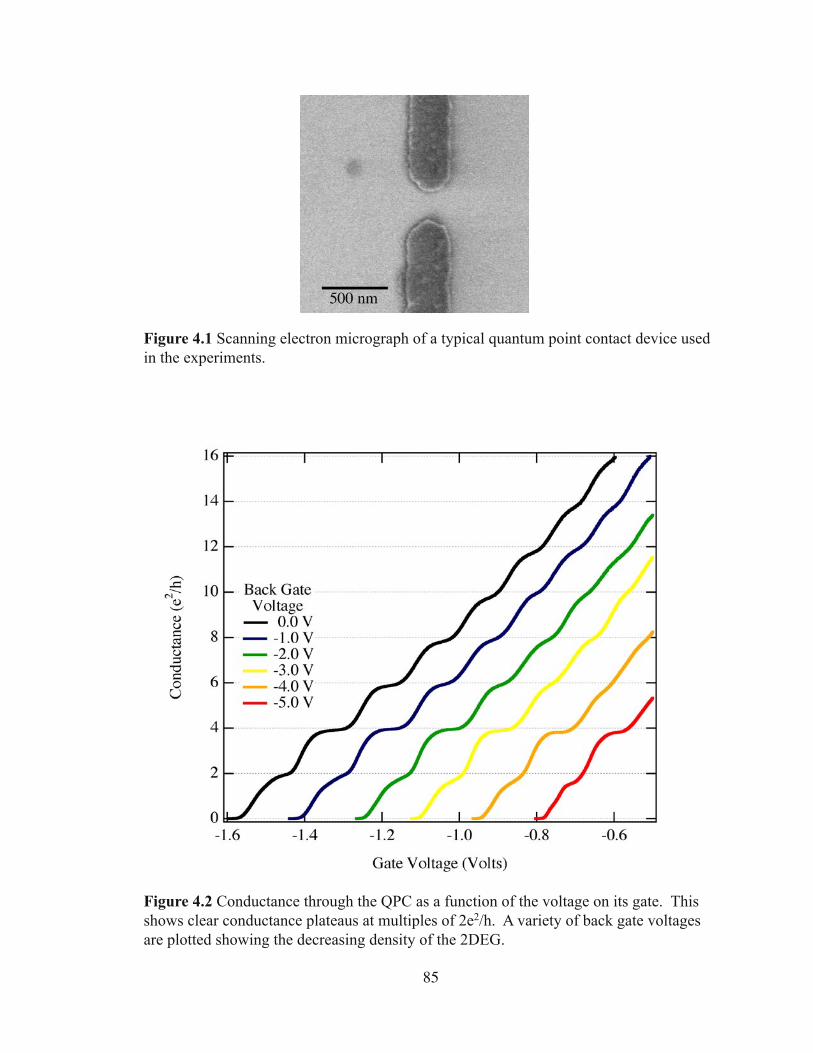
85
Figure 4.1 Scanning electron micrograph of a typical quantum point contact device used in the experiments.
Figure 4.2 Conductance through the QPC as a function of the voltage on its gate. This shows clear conductance plateaus at multiples of 2e2/h. A variety of back gate voltages are plotted showing the decreasing density of the 2DEG.

86
to each new quantum mode of the QPC becoming accessible as its width is opened. As
the back gate voltage is made more negative, the gate voltage required to pinch off the
QPC is less. This is because the density is being reduced requiring less gate voltage to
deplete the electron gas. The second reason is the width of the constriction must be larger
for the electrons to get through since their wavelength is increasing. As the density is
reduced, the plateaus no longer lie exactly on multiples of 2e2/h. This is due to increased
backscattering near the QPC, which reduces its conductance. The plateaus are also not as
well defined as the density decreases because the energy spacing between subbands of the
QPC decreases. The finite temperature of the measurement means that the electrons have
a spread in energy, which allows them to travel through multiple subbands causing the
plateaus to blur. Each step in the conductance is the Fermi function for the occupation of
the given mode of the QPC.
Before measuring the local electron density with our imaging technique, we have
characterized the effect of the back gate on the average density of the 2DEG. To study
the effect of the back gate voltage on the density, we have measured the density of the
2DEG using Shubnikov-de Haas oscillations. With a large perpendicular magnetic field
applied to the sample, the constant two-dimensional density of states becomes a series of
sharp peaks centered at the Landau levels. The positions of the Landau levels are given
by En = (n + 1/2)hω
c, where ω
c is the cyclotron frequency, ω
c = eB/m. The Shubnikov-
de Haas oscillations occur as each successive Landau level is emptied by increasing
the magnetic field. There is a dip in the longitudinal resistance when the Fermi energy
equals the energy of the Landau level giving oscillations that are periodic in the inverse
magnetic field. Figure 4.3 plots the measured change in longitudinal resistance as a
87
function of inverse magnetic field. This shows the Shubnikov-de Haas oscillations that
are periodic in inverse magnetic field. Their period gives the density of the 2DEG using
the formula ns = 2e/(h Δ(1/B)) where e is the electron charge, h is Planck’s constant and
Δ(1/B) is the period of the oscillations. This measurement was repeated for a series of
back gate voltages, which reduce the density. Figure 4.4 shows the effect of the back
gate voltage on the average density. Each of the Shubnikov-de Haas measurements
gives one of the data points in the plot of density versus back gate voltage. This data was
taken from a different piece of the same wafer as used in the imaging experiment. A four
terminal resistance measurement was also done to determine the resistivity of the 2DEG.
From the resistivity and the Shubnikov-de Haas measurement, the mobility as a function
Figure 4.3 Measured longitudinal resistance as a function of inverse magnetic field showing the Shubnikov-de Haas oscillations. These oscillations are periodic in the inverse magnetic field. Their period gives the electron density in the 2DEG.

88
of the density can be determined. This is plotted in Figure 4.5 showing a decrease in
mobility with decreasing electron density. This is due to the disordered background
Figure 4.4 Measured density as a function of back gate voltage, showing a linear decrease in density. This measurement was done using the Shubnikov-de Haas oscillations.
Figure 4.5 Measured mobility of the 2DEG as a function of the density. This shows the mobility decreasing due to the increasing scattering as the density is reduced.
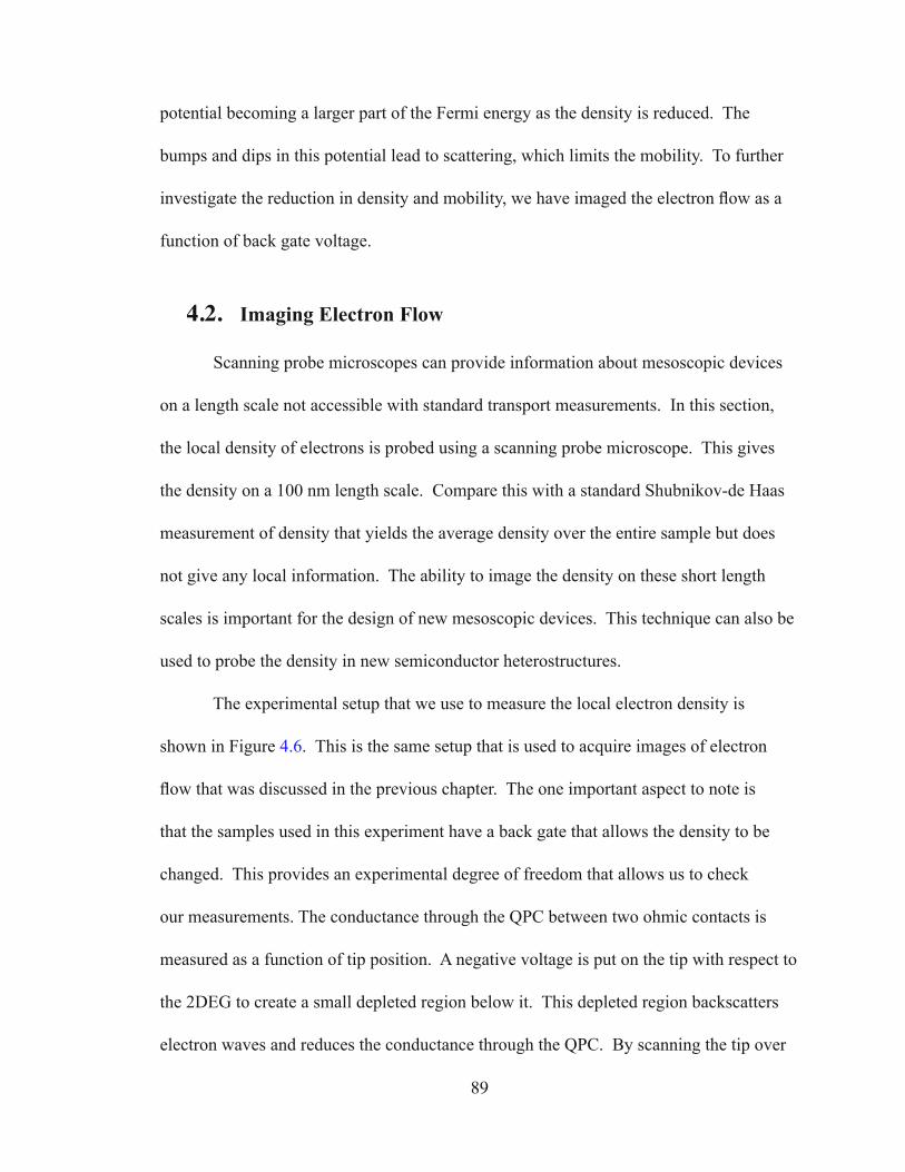
89
potential becoming a larger part of the Fermi energy as the density is reduced. The
bumps and dips in this potential lead to scattering, which limits the mobility. To further
investigate the reduction in density and mobility, we have imaged the electron flow as a
function of back gate voltage.
4.2. Imaging Electron Flow
Scanning probe microscopes can provide information about mesoscopic devices
on a length scale not accessible with standard transport measurements. In this section,
the local density of electrons is probed using a scanning probe microscope. This gives
the density on a 100 nm length scale. Compare this with a standard Shubnikov-de Haas
measurement of density that yields the average density over the entire sample but does
not give any local information. The ability to image the density on these short length
scales is important for the design of new mesoscopic devices. This technique can also be
used to probe the density in new semiconductor heterostructures.
The experimental setup that we use to measure the local electron density is
shown in Figure 4.6. This is the same setup that is used to acquire images of electron
flow that was discussed in the previous chapter. The one important aspect to note is
that the samples used in this experiment have a back gate that allows the density to be
changed. This provides an experimental degree of freedom that allows us to check
our measurements. The conductance through the QPC between two ohmic contacts is
measured as a function of tip position. A negative voltage is put on the tip with respect to
the 2DEG to create a small depleted region below it. This depleted region backscatters
electron waves and reduces the conductance through the QPC. By scanning the tip over
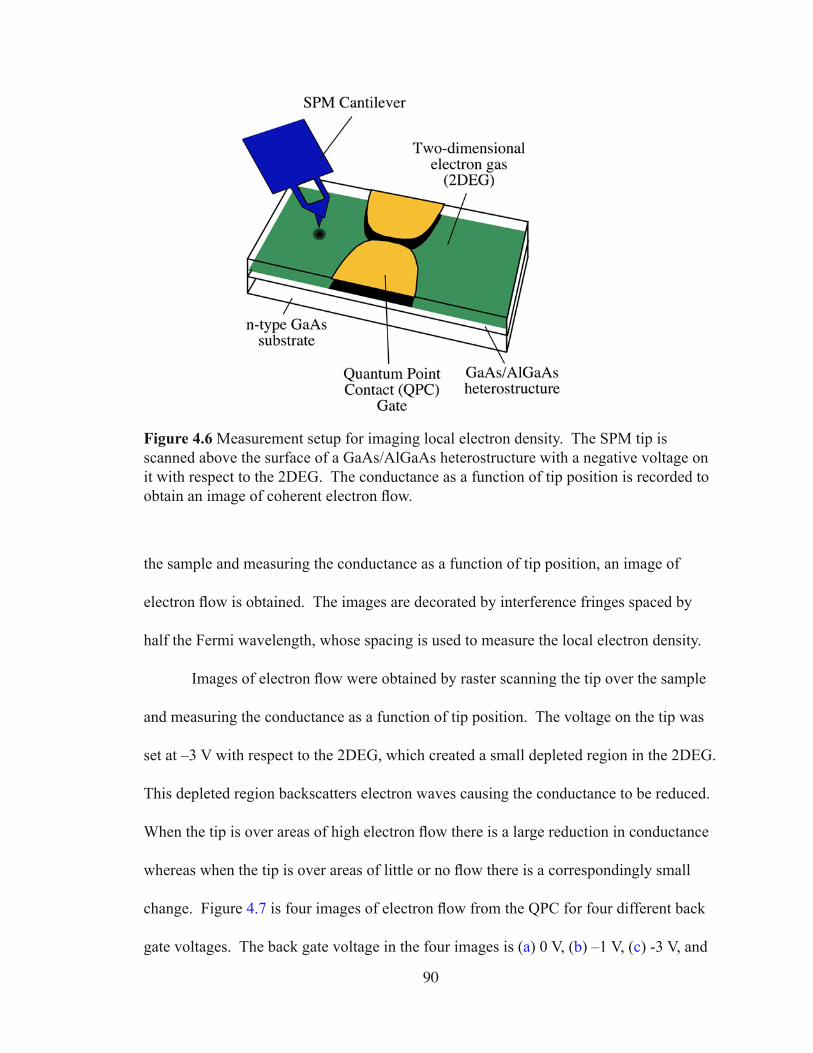
90
the sample and measuring the conductance as a function of tip position, an image of
electron flow is obtained. The images are decorated by interference fringes spaced by
half the Fermi wavelength, whose spacing is used to measure the local electron density.
Images of electron flow were obtained by raster scanning the tip over the sample
and measuring the conductance as a function of tip position. The voltage on the tip was
set at –3 V with respect to the 2DEG, which created a small depleted region in the 2DEG.
This depleted region backscatters electron waves causing the conductance to be reduced.
When the tip is over areas of high electron flow there is a large reduction in conductance
whereas when the tip is over areas of little or no flow there is a correspondingly small
change. Figure 4.7 is four images of electron flow from the QPC for four different back
gate voltages. The back gate voltage in the four images is (a) 0 V, (b) –1 V, (c) -3 V, and
Figure 4.6 Measurement setup for imaging local electron density. The SPM tip is scanned above the surface of a GaAs/AlGaAs heterostructure with a negative voltage on it with respect to the 2DEG. The conductance as a function of tip position is recorded to obtain an image of coherent electron flow.
91
Figure 4.7 Four images of electron flow from the QPC for different back gate voltages: (a) -0.0 V, (b) -1.0 V, (c) -3.0 V and (d) -5.0 V. These show the spacing of the interference fringes increasing and the flow becoming more diffuse.
92
(d) –5 V. These images show how the electron flow changes with back gate voltage.
The spacing of the interference fringes that decorate the images increases as the back
gate voltage decreases. This occurs because the fringes are spaced by half the Fermi
wavelength, which is being increased by the decreasing density. The second feature is
the strength of the branches of flow becomes less pronounced with decreasing back gate
voltage. This is due to the flow becoming more diffuse since the mobility and hence the
mean free path is being reduced. Each branch of current is scattered and split into new
branches more quickly since the mean free path is shorter. This leads to an image that no
longer shows the narrow branches of current and instead becomes more uniform.
4.3. Measuring Local Density
In order to measure the local electron density, we must extract the spacing of the
interference fringes while removing the background electron flow. Since the fringes are
spaced by half the Fermi wavelength, there is a simple relation between their spacing, d,
and the electron density, n. This relation is given by n = π/(2d2). A measurement of the
density turns into a measurement of the spacing of the interference fringes. To isolate
the interference fringes from the background flow, we used a spatial high pass filter.
The high pass filtering was done by smoothing the data to remove the fringes and then
subtracting this smoothed version from the original. The smoothing was done along the
direction perpendicular to the fringes in order to reduce the fringe amplitude without
changing the amplitude of the branches of electron flow. This filtering left only the high
frequency components in the original scan. This analysis was done for a small section
of each scan to isolate the interference fringes. Figure 4.8 shows the high pass filtered
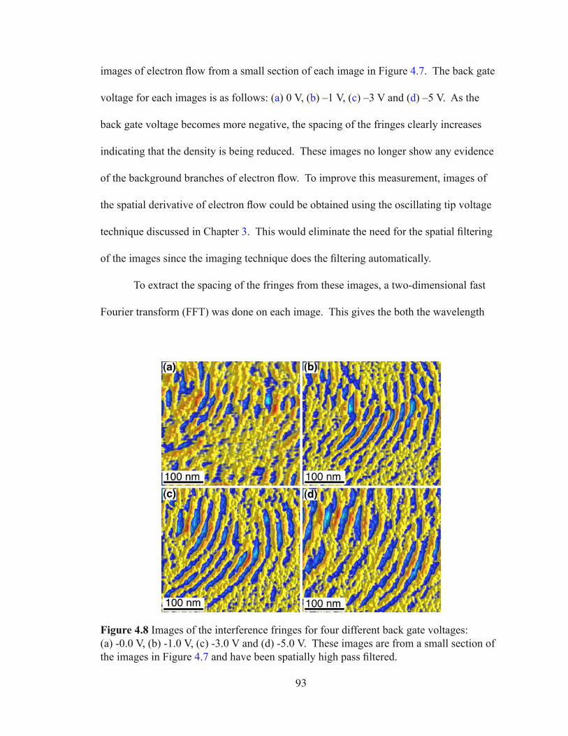
93
images of electron flow from a small section of each image in Figure 4.7. The back gate
voltage for each images is as follows: (a) 0 V, (b) –1 V, (c) –3 V and (d) –5 V. As the
back gate voltage becomes more negative, the spacing of the fringes clearly increases
indicating that the density is being reduced. These images no longer show any evidence
of the background branches of electron flow. To improve this measurement, images of
the spatial derivative of electron flow could be obtained using the oscillating tip voltage
technique discussed in Chapter 3. This would eliminate the need for the spatial filtering
of the images since the imaging technique does the filtering automatically.
To extract the spacing of the fringes from these images, a two-dimensional fast
Fourier transform (FFT) was done on each image. This gives the both the wavelength
Figure 4.8 Images of the interference fringes for four different back gate voltages: (a) -0.0 V, (b) -1.0 V, (c) -3.0 V and (d) -5.0 V. These images are from a small section of the images in Figure 4.7 and have been spatially high pass filtered.
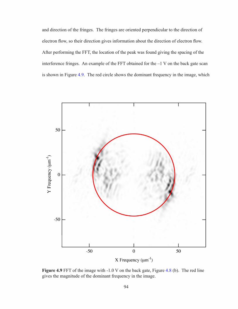
94
and direction of the fringes. The fringes are oriented perpendicular to the direction of
electron flow, so their direction gives information about the direction of electron flow.
After performing the FFT, the location of the peak was found giving the spacing of the
interference fringes. An example of the FFT obtained for the –1 V on the back gate scan
is shown in Figure 4.9. The red circle shows the dominant frequency in the image, which
Figure 4.9 FFT of the image with -1.0 V on the back gate, Figure 4.8 (b). The red line gives the magnitude of the dominant frequency in the image.

95
is at a constant distance from the center of the image. The radius of the circle was chosen
so that it passed through the peak in the FFT. We are only interested in the magnitude of
this frequency in order to obtain the wavelength of the fringes. To convert this frequency
into a wavelength of the electrons, we take the inverse of the magnitude. This gives the
spacing of the fringes, which is half of the wavelength.
This process was repeated for each of the scans to obtain the wavelength as a
function of back gate voltage. The scans were taken in steps of -1 V on the back gate
starting at 0 V. To convert the wavelength to density, we use the formula n = π/2d2, where
d is the fringe spacing. The density in each of the scans is plotted in Figure 4.10. This
shows that the density decreases linearly with back gate voltage starting slightly below
4.0 x 1011 cm-2.
Figure 4.10 Imaged density as a function of the back gate voltage. The circles were found using the FFT technique discussed in the text. The solid line is the expected change in density from a capacitor model.
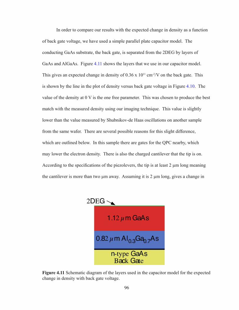
96
In order to compare our results with the expected change in density as a function
of back gate voltage, we have used a simple parallel plate capacitor model. The
conducting GaAs substrate, the back gate, is separated from the 2DEG by layers of
GaAs and AlGaAs. Figure 4.11 shows the layers that we use in our capacitor model.
This gives an expected change in density of 0.36 x 1011 cm-2/V on the back gate. This
is shown by the line in the plot of density versus back gate voltage in Figure 4.10. The
value of the density at 0 V is the one free parameter. This was chosen to produce the best
match with the measured density using our imaging technique. This value is slightly
lower than the value measured by Shubnikov-de Haas oscillations on another sample
from the same wafer. There are several possible reasons for this slight difference,
which are outlined below. In this sample there are gates for the QPC nearby, which
may lower the electron density. There is also the charged cantilever that the tip is on.
According to the specifications of the piezolevers, the tip is at least 2 µm long meaning
the cantilever is more than two µm away. Assuming it is 2 µm long, gives a change in
Figure 4.11 Schematic diagram of the layers used in the capacitor model for the expected change in density with back gate voltage.
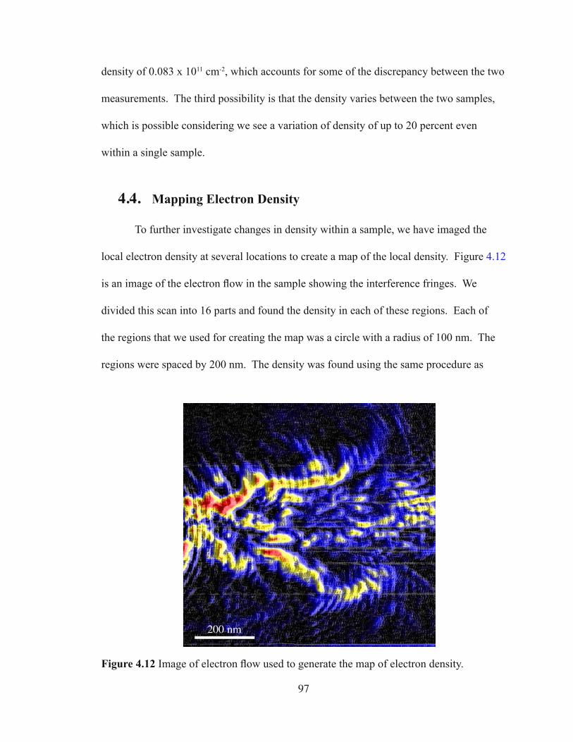
97
density of 0.083 x 1011 cm-2, which accounts for some of the discrepancy between the two
measurements. The third possibility is that the density varies between the two samples,
which is possible considering we see a variation of density of up to 20 percent even
within a single sample.
4.4. Mapping Electron Density
To further investigate changes in density within a sample, we have imaged the
local electron density at several locations to create a map of the local density. Figure 4.12
is an image of the electron flow in the sample showing the interference fringes. We
divided this scan into 16 parts and found the density in each of these regions. Each of
the regions that we used for creating the map was a circle with a radius of 100 nm. The
regions were spaced by 200 nm. The density was found using the same procedure as
Figure 4.12 Image of electron flow used to generate the map of electron density.

98
in the previous section for the different back gate voltages. An example of two of the
regions used in generating the density map and their FFTs is shown in Figure 4.13. In
each FFT, there is a circle that gives the maximum signal, which is shown in red. The
radius of this circle was taken as the spacing of the interference fringes for this region
when calculating the local density of the image. For the two FFTs, the peak value along
this red circle occurs at different values of fx and f
y indicating that the electron flow is
pointed in different directions in the two images. The value of the x and y coordinates of
the peak were used to determine the direction of electron flow in the region. Figure 4.14
plots the measured density at each of the 16 locations. A linear interpolation was done
between each of the points to produce the map of electron density. The arrows in the
image represent the direction of electron flow at that location based on the direction
of the fringes. From this map of electron density, we found an average density of
2.95 x 1011 cm-2. This average density is in fairly good agreement with our previous
imaging and Shubnikov-de Hass measurements. The measured density had a standard
deviation of about 15 percent. This is fairly consistent with the simulations done by Scot
Shaw [Shaw, (2002)] of the expected variation in density due to the random placement
and ionization of donor atoms.
In summary, we have developed a technique for imaging the local electron density
in a 2DEG. The technique relies on measuring the interference fringes in images of
electron flow to obtain the local Fermi wavelength and hence the density. We are able
to image spatial variations in the density on a scale of about 100 nm. The results for the
change in density as a function of back gate voltage are in excellent agreement with a
parallel plate capacitor model. We have also mapped the variation in the density due to
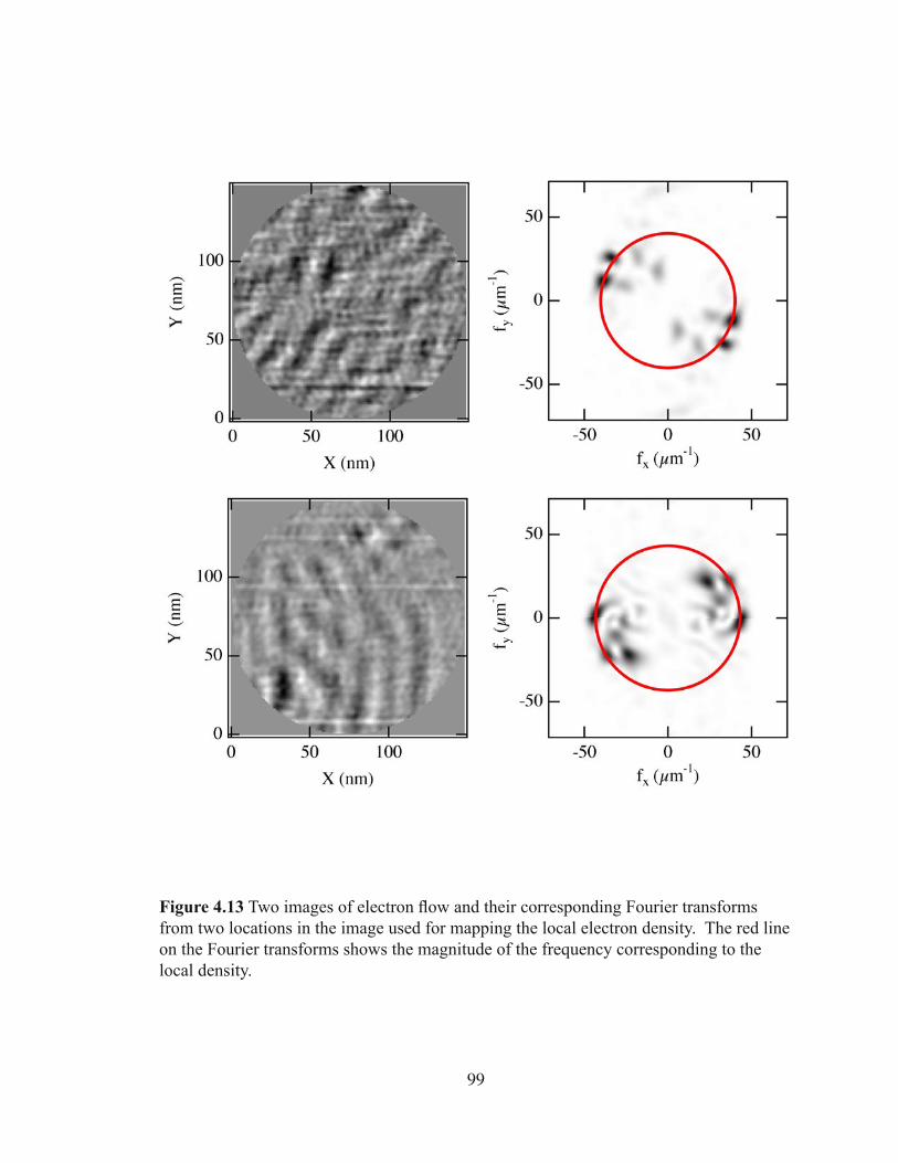
99
Figure 4.13 Two images of electron flow and their corresponding Fourier transforms from two locations in the image used for mapping the local electron density. The red line on the Fourier transforms shows the magnitude of the frequency corresponding to the local density.
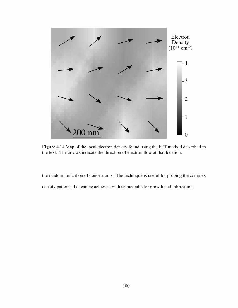
100
the random ionization of donor atoms. The technique is useful for probing the complex
density patterns that can be achieved with semiconductor growth and fabrication.
Figure 4.14 Map of the local electron density found using the FFT method described in the text. The arrows indicate the direction of electron flow at that location.

101
Chapter 5
Imaging Electron Energy Loss
In this chapter, we demonstrate a technique for measuring the electron-
electron scattering rate in a two-dimensional electron gas using our imaging technique.
Section 5.1 describes the technique, which involves measuring the decay of the
backscattered signal as a function of the applied source-drain voltage. Section 5.2
presents images of electron flow for different applied source-drain voltages. The images
of electron flow show the signal decreasing for increasing source-drain voltage indicating
an increased scattering rate. Images are acquired as a function of distance and Fermi
energy, showing increasing scattering with distance and decreasing Fermi energy. A
comparison of all of the results with the theory for electron-electron scattering in a 2DEG
is done in section 5.3. The results are in good agreement with the theory as a function of
distance and energy.
The ability to image electron energy loss is important for the design and
understanding of new devices that rely on the coherence of the electron. There has
been much experimental interest in studying the energy loss of electrons in 2DEGs
through electron-electron scattering [Yacoby, (1991); Muller, (1995), Schäpers, (1995);
Predel, (2000)], electron-phonon scattering [Sivan, (1989)] and other mechanisms.
However, in all of these experiments it has been very difficult to obtain spatial
information about the scattering mechanisms. Most of the experiments have a fixed
geometry, which does not allow for the study of the spatial dependence of the scattering
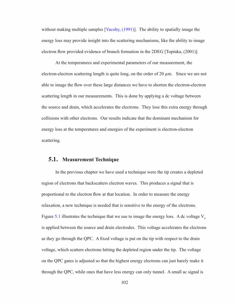
102
without making multiple samples [Yacoby, (1991)]. The ability to spatially image the
energy loss may provide insight into the scattering mechanisms, like the ability to image
electron flow provided evidence of branch formation in the 2DEG [Topinka, (2001)].
At the temperatures and experimental parameters of our measurement, the
electron-electron scattering length is quite long, on the order of 20 µm. Since we are not
able to image the flow over these large distances we have to shorten the electron-electron
scattering length in our measurements. This is done by applying a dc voltage between
the source and drain, which accelerates the electrons. They lose this extra energy through
collisions with other electrons. Our results indicate that the dominant mechanism for
energy loss at the temperatures and energies of the experiment is electron-electron
scattering.
5.1. Measurement Technique
In the previous chapter we have used a technique were the tip creates a depleted
region of electrons that backscatters electron waves. This produces a signal that is
proportional to the electron flow at that location. In order to measure the energy
relaxation, a new technique is needed that is sensitive to the energy of the electrons.
Figure 5.1 illustrates the technique that we use to image the energy loss. A dc voltage V0
is applied between the source and drain electrodes. This voltage accelerates the electrons
as they go through the QPC. A fixed voltage is put on the tip with respect to the drain
voltage, which scatters electrons hitting the depleted region under the tip. The voltage
on the QPC gates is adjusted so that the highest energy electrons can just barely make it
through the QPC, while ones that have less energy can only tunnel. A small ac signal is

103
added to the dc voltage across the QPC to use for lockin detection. This lockin detection
mechanism ensures that the measurement is only sensitive to electrons in a narrow energy
band. An image of the conductance as a function of tip position is recorded. In order to
understand the images of electron flow, we have to consider two cases: the electron goes
from the QPC to the tip and back without losing any energy and it loses some energy on
this roundtrip. The two cases are shown in Figure 5.2. In the first case, Figure 5.2 (a),
the electron has not lost any energy and will be able to go back through the QPC. This
backscattering will cause a reduction in the conductance when the tip is present. In the
second case, Figure 5.2 (b), the electron loses energy during the roundtrip and can no
longer go back through the QPC. Therefore, there will be no signal from this electron
and no image of electron flow. By measuring the strength of the electron flow as a
Figure 5.1 Illustrates the technique used for imaging electron flow with an applied dc bias. The voltage on the tip and gates are held fixed with enough voltage on the tip to deplete the electron gas. A dc bias is applied to one side of the QPC with a small ac voltage to achieve energy selectivity.

104
function of distance, the rate of electron energy loss is determined. The measurement
of the electron flow is done by recording the differential conductance, g = ∂I/∂Vds
as a
function of tip position. We are interested in how much the flow changes when the tip
is present so the relevant quantity is the change in differential conductance Δg. This is
found by subtracting the signal when the tip is present from the signal without the tip.
As the distance from the tip to QPC increases, there is more time for the electron to lose
energy and the signal should become weaker. The signal should also become weaker as
the dc bias V0 is increased because the electron has more available states to scatter into,
which increases its scattering rate.
5.2. Images of Electron Flow
Figure 5.3 shows two images of electron flow from the same area. Figure 5.3 (a)
has no dc voltage V0 applied across the QPC and Figure 5.3 (b) has V
0 = 2.4 mV applied
Figure 5.2 Illustrates the mechanism used for dc bias imaging. In (a) the electron does not scatter in the roundtriup from the tip to the QPC and therefore the tip reduces the conductance. In (b) the electron loses energy due to a scattering event and can not go back through the QPC. This eliminates the backscattered signal from the tip.
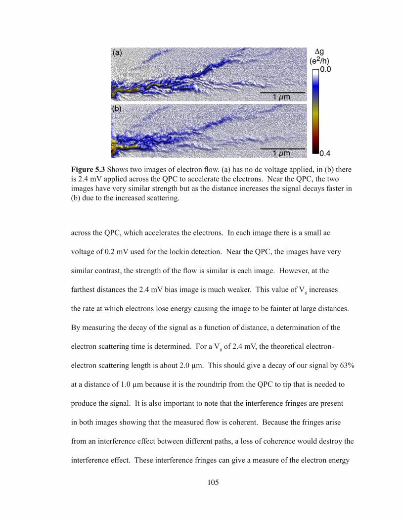
105
across the QPC, which accelerates the electrons. In each image there is a small ac
voltage of 0.2 mV used for the lockin detection. Near the QPC, the images have very
similar contrast, the strength of the flow is similar is each image. However, at the
farthest distances the 2.4 mV bias image is much weaker. This value of V0 increases
the rate at which electrons lose energy causing the image to be fainter at large distances.
By measuring the decay of the signal as a function of distance, a determination of the
electron scattering time is determined. For a V0 of 2.4 mV, the theoretical electron-
electron scattering length is about 2.0 µm. This should give a decay of our signal by 63%
at a distance of 1.0 µm because it is the roundtrip from the QPC to tip that is needed to
produce the signal. It is also important to note that the interference fringes are present
in both images showing that the measured flow is coherent. Because the fringes arise
from an interference effect between different paths, a loss of coherence would destroy the
interference effect. These interference fringes can give a measure of the electron energy
Figure 5.3 Shows two images of electron flow. (a) has no dc voltage applied, in (b) there is 2.4 mV applied across the QPC to accelerate the electrons. Near the QPC, the two images have very similar strength but as the distance increases the signal decays faster in (b) due to the increased scattering.

106
because they are spaced by half the Fermi wavelength as discussed in Chapter 4.
As the dc bias V0 is increased, the electrons have extra energy and hence a shorter
wavelength. Figure 5.4 plots the electron wavelength as a function of V0. This is done
for two different distances from the QPC. The red circles are one µm away and the blue
triangles are two µm away. The value of the wavelengths was determined using a Fourier
transform method. A one-dimensional line sample was taken perpendicular to the fringes.
The FFT of this one-dimensional sample was found to give the spacing of the interference
fringes. The solid line is a fit to the expected change in wavelength as a function of
Figure 5.4 Plot of the measured wavelength of the electrons versus the applied dc voltage for two distances from the QPC. The black line is the expected wavelength based on the Fermi energy and applied voltage. This graph shows that the wavelength of the electron increases with the applied voltage as expected.

107
excess applied voltage. The wavelength shifts because the applied voltage V0 is added to
the energy of the electron. This gives the following equation for the wavelength versus
applied voltage.
The expected fringes spacing is in very good agreement with the measured wavelength
as a function of applied bias voltage. There is one free parameter in this fit, which is the
Fermi energy of the 2DEG. At each of the two distances, the value needed for the best
fit is within 2% of the measured Fermi energy for the scan without any excess applied
voltage. There is a difference in the wavelength for the two distances, which may arise
from the fall off in the potential from the QPC gate. The potential of the gate falls off
fairly slowly leaving some portion even at one micron. Another possible explanation is a
variation in the local electron density as discussed in section 4.4. This result shows that
the electrons are being accelerated by the excess energy applied across the QPC.
To further investigate the distance dependence of the electron energy loss, we
have looked at three small regions of the electron flow. These are located at three
different distances from the QPC. The closest one is at 0.6 µm, followed by 1.0 µm and
the farthest is at 1.4 µm. Figure 5.5 shows the electron flow at these three locations for
four different dc bias voltages V0 at a temperature of 1.7 K. The color scale is the change
in differential conductance, Δg for the given tip position. The distance from the QPC
to the images is as follows (a-d) 0.6 µm, (e-h) 1.0 µm, and (i-l) 1.4 µm. Moving from
left to right, V0 goes from 0 mV up to 3 mV in steps of 1 mV. As the bias is increased
the strength of the signal decreases for all three distances. However, it decreases much
€
λ−1 = 2mh2
EF − eV0( )

108
Fig
ure
5.5
Imag
es o
f el
ectr
on fl
ow f
or th
ree
dist
ance
s an
d fo
ur d
c bi
as v
olta
ges
at a
tem
pera
ture
of
1.7
K.
The
row
s ar
e at
di
stan
ces
of 0
.6 µ
m, 1
.0 µ
m a
nd 1
.4 µ
m.
The
col
umns
hav
e th
e fo
llow
ing
appl
ied
dc v
olta
ges
V0 0
mV
, 1 m
V, 2
mV
and
3m
V.
The
sig
nal d
ecay
s fo
r in
crea
sing
dc
volta
ge a
nd in
crea
sing
dis
tanc
e

109
more quickly at the longest distance compared to the shortest one. At 1.4 µm and 3 mV,
Figure 5.5 (l), we see almost no signal; it is primarily noise. This is in contrast to 0.6 µm
and 3 mV, Figure 5.5 (d), where the signal is still quite strong. This shows that the
electrons are losing their excess energy as they make the 2.8 µm roundtrip from the tip
to the QPC in this image. However, in the shorter distance, the electron is less likely
to undergo a scattering event and therefore the signal is not decaying as fast. To fully
characterize the electron-electron scattering analysis of the signal as a function of the
excess applied energy is necessary.
A detailed study of the energy dependence of the signal was done by looking at
the electron flow image as a function of the applied dc bias V0. This was done at the
same three locations as discussed earlier. To investigate the energy dependence, the
average change in conductance was measured as a function of V0. This average change
€
∆g was found by averaging the measured signal over the entire scan area. This generates
one data point of
€
∆g for each value of V0. Figure 5.6 plots this measured
€
∆g versus
bias voltage V0. There are three sets of data for the three different distances. Each of
the values in the plot has been normalized to the value without any dc bias. This means
that each curve starts at 1 in the center. The three curves have been offset from each
other for clarity. In all three cases, the measured signal decreases with increasing energy.
However, as the distance increases the signal decreases more quickly indicating that more
scattering has occurred. This is in agreement with expectations because the electron has a
longer time to scatter for the longer distances.
After studying the distance dependence of the electron-electron scattering, we
looked at the effect of changing the Fermi energy of the electrons. For a fixed excess

110
energy, reducing the Fermi energy increases the scattering rate because the excess energy
becomes a larger fraction of the total energy. This means more of the filled states may
participate in the scattering, which increases the scattering rate. We have repeated these
measurements at the middle distance 1.0 µm for a series of Fermi energies. In this case,
we have used a back gate voltage, which reduces the density of the 2DEG and lowers the
Fermi energy. As the back gate voltage increases, the Fermi energy is reduced and the
Figure 5.6 Plot of the average measured signal as a function of applied dc voltage V0 for
three different distances from the QPC. The solid lines are the expected decrease in the signal due to electron-electron scattering at the given distance and value of V
0 given a
Fermi energy of 15 meV . All of the curves have been normalized to their value at V0 = 0
meV and offset by 0.2 for clarity.
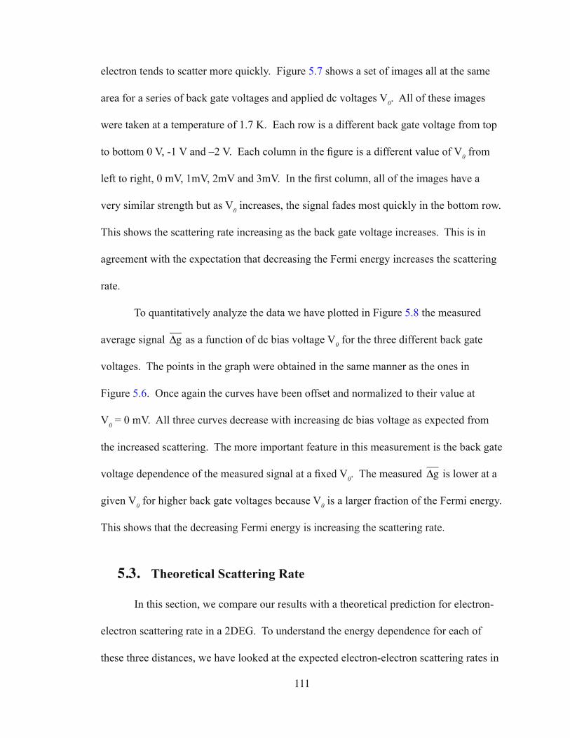
111
electron tends to scatter more quickly. Figure 5.7 shows a set of images all at the same
area for a series of back gate voltages and applied dc voltages V0. All of these images
were taken at a temperature of 1.7 K. Each row is a different back gate voltage from top
to bottom 0 V, -1 V and –2 V. Each column in the figure is a different value of V0 from
left to right, 0 mV, 1mV, 2mV and 3mV. In the first column, all of the images have a
very similar strength but as V0 increases, the signal fades most quickly in the bottom row.
This shows the scattering rate increasing as the back gate voltage increases. This is in
agreement with the expectation that decreasing the Fermi energy increases the scattering
rate.
To quantitatively analyze the data we have plotted in Figure 5.8 the measured
average signal
€
∆g as a function of dc bias voltage V0 for the three different back gate
voltages. The points in the graph were obtained in the same manner as the ones in
Figure 5.6. Once again the curves have been offset and normalized to their value at
V0 = 0 mV. All three curves decrease with increasing dc bias voltage as expected from
the increased scattering. The more important feature in this measurement is the back gate
voltage dependence of the measured signal at a fixed V0. The measured
€
∆g is lower at a
given V0 for higher back gate voltages because V
0 is a larger fraction of the Fermi energy.
This shows that the decreasing Fermi energy is increasing the scattering rate.
5.3. Theoretical Scattering Rate
In this section, we compare our results with a theoretical prediction for electron-
electron scattering rate in a 2DEG. To understand the energy dependence for each of
these three distances, we have looked at the expected electron-electron scattering rates in
112
Fig
ure
5.7
Imag
es o
f el
ectr
on fl
ow f
or th
ree
back
gat
e vo
ltage
and
fou
r dc
bia
s vo
ltage
s V
0. T
he r
ows
are
at b
ack
gate
vol
tage
s of
0 V
olts
, -1
Vol
ts a
nd -
2 V
olts
. T
he c
olum
ns h
ave
the
follo
win
g va
lues
of V
0 0 m
V, 1
mV
, 2 m
V a
nd 3
mV
. A
s th
e ba
ck g
ate
volta
ge is
incr
ease
d, th
e si
gnal
dec
ays
mor
e qu
ickl
y. A
ll of
the
imag
es w
ere
take
n at
a te
mpe
ratu
re o
f 1.
7 K
.

113
a 2DEG. This is the dominant scattering mechanism at these temperatures and energies
in the 2DEG. Giuliani and Quinn have calculated the scattering time as a function of
the excess applied voltage V0 at T = 0 K [Giuliani, (1982)]. They found the following
equation for the scattering time, τee
€
1τ ee
= EF
4πheV0EF
2
ln EF
eV0
+ ln
2qTFpF
+
12
Figure 5.8 Plot of the average measured signal as a function of applied dc voltage V0 for
three different back gate voltages, which reduce the Fermi energy. The solid lines are the expected decrease in the signal due to electron-electron scattering at 1.0 µm for the given V
0 and back gate voltage. All of the curves have been normalized to their value at
V0 = 0 meV and offset by 0.2 for clarity.

114
In this equation, EF is the Fermi energy, p
F is the momentum and q
TF is the Thomas-Fermi
screening vector in two dimensions. This equation gives a good approximation of the
electron-electron scattering rate as long as the excess energy is much larger than the
temperature. This is true for our large bias voltages since kT = 0.141 meV. Since the
measured signal
€
∆g requires that the electron has not undergone a scattering event, we
want the probability that an electron can travel a distance L without scattering. Because
the chance of an electron scattering is random and they remain ballistic over the range of
our measurement, the probability that an electron will not have scattered is given by the
exponential decay.
where v is the velocity after the electrons pass through the QPC and τee
is the scattering
rate. This gives an approximately Gaussian distribution in the applied voltage V0, since
τee
goes as V0
-2. The probability distribution is plotted in Figure 5.6 for the three different
distances from the QPC. There are no free parameters in the plotting of the probability
distribution because L is given by the area of the image, the applied voltage V0 is known,
and EF = 15 meV is measured. There is qualitative agreement between the data and the
expected distributions; the measured signal decays more quickly at longer distances. For
the shortest distance, there is a larger discrepancy between the experiment and theory.
This may be caused because the electrons have not been fully accelerated at such a short
distance from the QPC. There is also an asymmetry in the bias direction, which may be
caused by the shape of the QPC constriction.
We have also plotted the expected decrease in the signal as a function of V0 for
€
P∝ exp −Lvτ ee
115
the three different back gate voltages. This is shown by the solid lines in Figure 5.7.
As in the previous figure there are no free parameters in the fit of the expected versus
measured distributions. The measured values for L = 1.0 µm, the applied voltage V0, and
Fermi energy EF are used. Once again, there is good qualitative agreement between the
experimental points and the theoretical curve showing that electron-electron scattering is
the dominant energy loss mechanism. The scattering rate increases as the Fermi energy
decreases.
These measurements demonstrate our technique’s ability to image electron energy
loss in a two-dimensional electron gas. We have shown that in our experiment the
dominant energy loss mechanism is electron-electron scattering. The results show good
agreement between experiment and theory for the electron-electron scattering rate at a
variety of distances and energies. This technique can be extended to measure electron
energy loss mechanisms at higher excess energies where electron-phonon scattering
becomes important. The technique can also be used in different geometries like quantum
wires and dots to provide insight into the energy loss mechanisms in these confined
geometries.

116
Chapter 6
Electron Optics
In this chapter, we examine the electron flow through electron-optic devices.
These are devices that are made with electrostatic gates on the surface to control the flow
of electrons through them. We have looked at several different devices to understand
how electron waves flow through them. We have studied a prism, a circular scatterer and
a channel. In section 6.1, we examine the electrostatic prism device. A small voltage
on the prism gate changes the density underneath and changes the direction of electrons
passing under it. Section 6.2 shows the results from a circular scatterer. The device is
created by a circular electrostatic gate on the surface, which acts as a defocusing lens or a
circular scatterer sending electron waves off in all directions depending on the voltage on
the gate. We have looked at this device to understand the scattering from the tip, which
also looks like a circular scatterer in the 2DEG. In section 6.3, we have studied a narrow
channel created in the two-dimensional electron gas (2DEG). This is created by two
electrostatic gates that confine the electrons. We are able to study the potential profile
from these gates by looking at the pattern of electron flow.
Electron-optic devices have been studied for many years in 2DEGs
[Spector, (1992)]. These devices rely on the ballistic transport of the electron from
an injector to a collector. As the mobility of 2DEGs improves and hence their mean
free path increases, the size of the devices can increase. Some of the devices that
have been studied are an absorber [Spector, (1990a)], a switch [Spector, (1990b)],
117
a lens [Sivan, (1990)], a beam crosser [Spector, (1991)] and an elliptical reflector
[Heremans, (1999)]. None of these devices work as well as expected for ideal ballistic
flow of electrons due to the small background potential of the donor atoms, which leads
to small angle scattering. The potential profile of the electrostatic gates also can degrade
the performance of the devices. By studying these devices with an imaging technique the
pattern of electron flow is obtained and the effect of the donors atoms and electrostatic
gates can be understood.
We have fabricated and measured several different devices all of which use a
quantum point contact (QPC) as an injector. The electron flow through the devices
is studied using a low temperature scanning probe microscope (SPM) as described in
Chapter 3. A negative voltage is put on the SPM tip with respect to the 2DEG to create
a small depleted region. This depleted region backscatters electrons to the QPC, which
reduces the conductance when the tip is over areas of high electron flow. By measuring
the change in conductance as a function of tip position, an image of electron flow is
obtained. We have imaged the electron flow through each device to illustrate their
operation and understand the effect of the gates and donor atoms on their performance.
6.1. Electrostatic Prism
In this experiment, we have used an electrostatic prism to control the direction
of electron flow in the 2DEG. Figure 6.1 is a colorized scanning electron micrograph of
the device used in the experiment. It consists of a quantum point contact (QPC) on the
right and a wedge shaped electrostatic gate that acts as a prism. The front edge of the
prism gate is located 1 µm to the left of the QPC. The voltage on this prism gate controls

118
the direction of electrons as they leave the area under the gate. Figure 6.2 illustrates the
idea behind using an electrostatic gate to change the direction of electron flow. There
Figure 6.1 Scanning electron microscope image of the electrostatic prism device. It consists of a quantum point contact on the right and a triangular shaped prism gate located 1 µm to the left.
Figure 6.2 Schematic diagram showing what happens to an incoming electron wave when it hits the region of reduced density under the prism gate. The electron trajectory is bent away from the normal.

119
are two different regions of the 2DEG, one that has a gate on it and another that does
not. A voltage is put on the gate, which changes the density of the 2DEG underneath
and also the momentum of the electrons. As electrons travel through the ungated 2DEG
and impinge on this area of changed density, they must conserve their momentum along
the interface between the two regions. This means that all of the change in momentum
occurs along the axis normal to the interface and the direction of the electron is changed.
The equation for the conservation of momentum gives the following simple relation
between the incoming and outgoing angle of the electron
where p1 and p
2 are the incoming and outgoing momentums and θ
1 and θ
2 are the two
angles. Using the fact that the square of the momentum in the 2DEG is proportional to
the density, this equation can be rewritten as
where n1 and n
2 are the densities in the two different regions. In this form, it is clear that
this is just an electron analog of Snell’s law in optics, where the density of the 2DEG is
analogous to the index of refraction. When an electron goes from an area of low density
to one of higher density it will be bent towards the normal.
We have imaged the electron flow after it travels under the prism gate for a series
of different voltages on the gate. As the voltage on the gate is made more negative, the
density is reduced causing the flow to bend towards the normal. This is the opposite
of light entering vacuum from glass where the light bends away from the normal. This
type of device can be used as a switch to control the flow of electrons [Spector, (1990b)].
A change in the voltage on the prism changes where the electrons go. If there are two
€
p1sin θ1( ) = p2sin θ2( )
€
n1sin θ1( ) = n2sin θ2( )

120
collectors then the electron flow can be shifted from one of them to the other causing the
current to switch. We are able to change the density under the prism from slightly above
the density of the 2DEG all the way down to 0. When the density is reduced the electrons
can no longer pass under the gate and all of the flow is reflected at the front edge of the
prism.
Figure 6.3 shows three images of electron flow from the prism device for
(a) +0.1 V, (b) 0.0 V, and (c) –0.1 V on the prism. These images were taken on the
second plateau of the QPC giving three main lobes of current. The images show the
flow bending upwards as the voltage is made more negative on the gate. The lines on the
images are the expected bending of the electrons for the three different prism voltages
shown. The dark line on each image is the expected bending for that voltage, while the
white lines are the bending for the other two voltages. This shows fairly good agreement
between the measured bending of the electron flow and the expected bending.
To further emphasize the change in flow with prism voltage, Figure 6.4 shows
two images of coherent flow at different prism voltages subtracted from each other.
This highlights the difference between the two images. We have subtracted the image
of electron flow with –0.1 V on the prism image, Figure 6.3 (c), from one with +0.1 V,
Figure 6.3 (a). The areas in red are stronger in the –0.1 V image while the blue areas are
stronger in the +0.1 V image. The white areas were the same in both images showing
that there is no change in the current. This shows that the flow bends upwards when the
voltage is made more negative.
We have demonstrated the operation of an electrostatic prism in a 2DEG by
imaging the coherent electron flow that passes under the prism gate. These images show

121
Fig
ure
6.3
Thr
ee im
ages
of
elec
tron
flow
for
dif
fere
nt v
olta
ges
on th
e el
ectr
osta
tic p
rism
gat
e, (
a) +
0.1
V, (
b) 0
.0 V
and
(c)
-0.
1 V
. T
he li
nes
on th
e im
ages
rep
rese
nt th
e ex
pect
ed d
irec
tion
of e
lect
ron
flow
for
the
thre
e di
ffer
ent g
ate
volta
ges.
The
bla
ck li
ne is
the
dire
ctio
n fo
r th
e gi
ven
imag
e. A
s th
e vo
ltage
on
the
pris
m is
mad
e m
ore
nega
tive
the
elec
tron
flow
is d
irec
ted
mor
e up
war
ds.
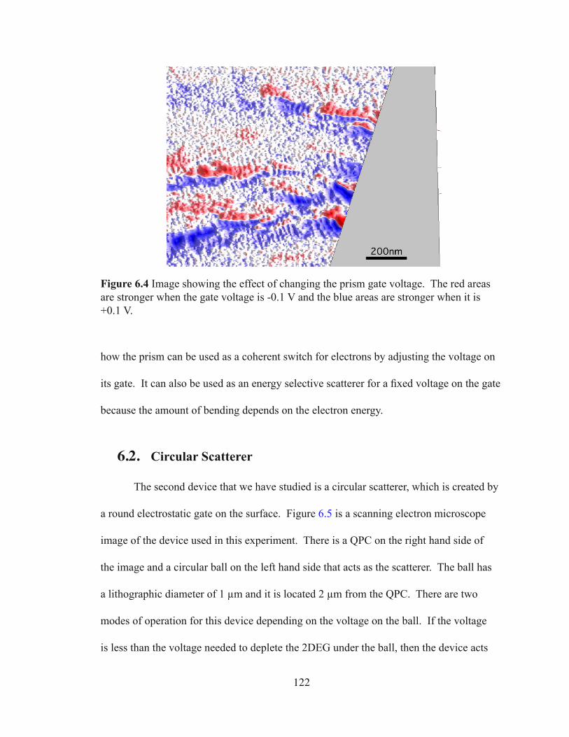
122
how the prism can be used as a coherent switch for electrons by adjusting the voltage on
its gate. It can also be used as an energy selective scatterer for a fixed voltage on the gate
because the amount of bending depends on the electron energy.
6.2. Circular Scatterer
The second device that we have studied is a circular scatterer, which is created by
a round electrostatic gate on the surface. Figure 6.5 is a scanning electron microscope
image of the device used in this experiment. There is a QPC on the right hand side of
the image and a circular ball on the left hand side that acts as the scatterer. The ball has
a lithographic diameter of 1 µm and it is located 2 µm from the QPC. There are two
modes of operation for this device depending on the voltage on the ball. If the voltage
is less than the voltage needed to deplete the 2DEG under the ball, then the device acts
Figure 6.4 Image showing the effect of changing the prism gate voltage. The red areas are stronger when the gate voltage is -0.1 V and the blue areas are stronger when it is +0.1 V.
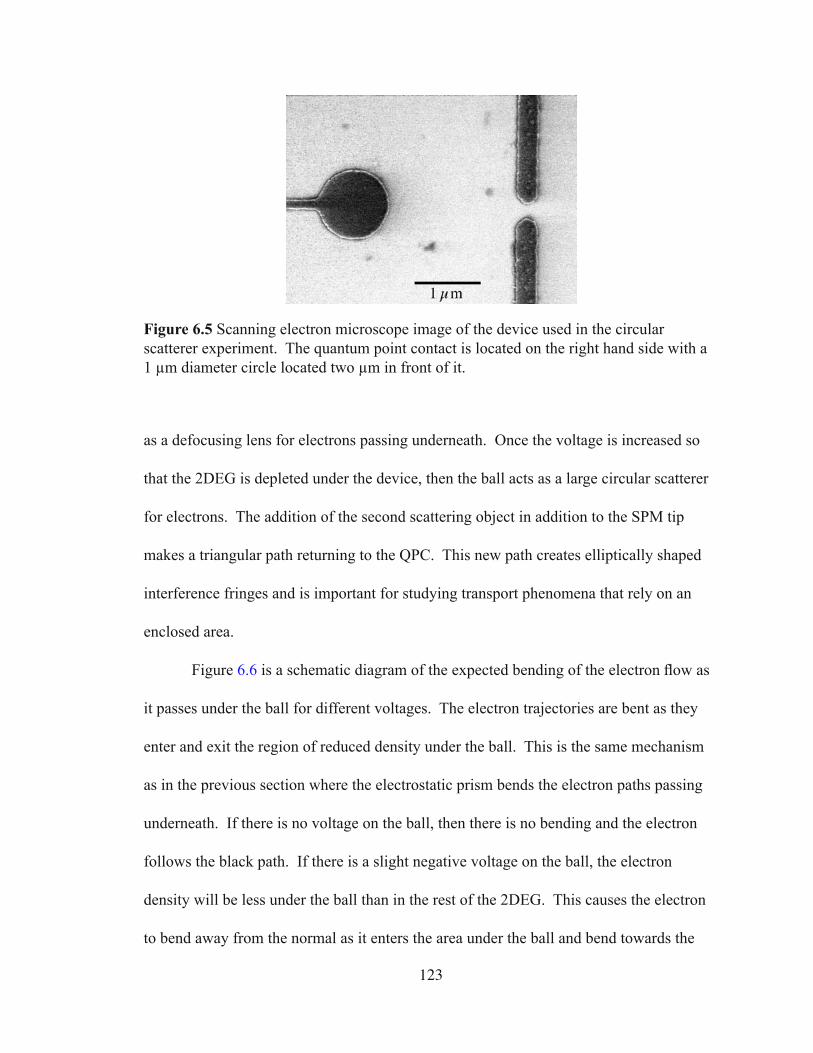
123
as a defocusing lens for electrons passing underneath. Once the voltage is increased so
that the 2DEG is depleted under the device, then the ball acts as a large circular scatterer
for electrons. The addition of the second scattering object in addition to the SPM tip
makes a triangular path returning to the QPC. This new path creates elliptically shaped
interference fringes and is important for studying transport phenomena that rely on an
enclosed area.
Figure 6.6 is a schematic diagram of the expected bending of the electron flow as
it passes under the ball for different voltages. The electron trajectories are bent as they
enter and exit the region of reduced density under the ball. This is the same mechanism
as in the previous section where the electrostatic prism bends the electron paths passing
underneath. If there is no voltage on the ball, then there is no bending and the electron
follows the black path. If there is a slight negative voltage on the ball, the electron
density will be less under the ball than in the rest of the 2DEG. This causes the electron
to bend away from the normal as it enters the area under the ball and bend towards the
Figure 6.5 Scanning electron microscope image of the device used in the circular scatterer experiment. The quantum point contact is located on the right hand side with a 1 µm diameter circle located two µm in front of it.
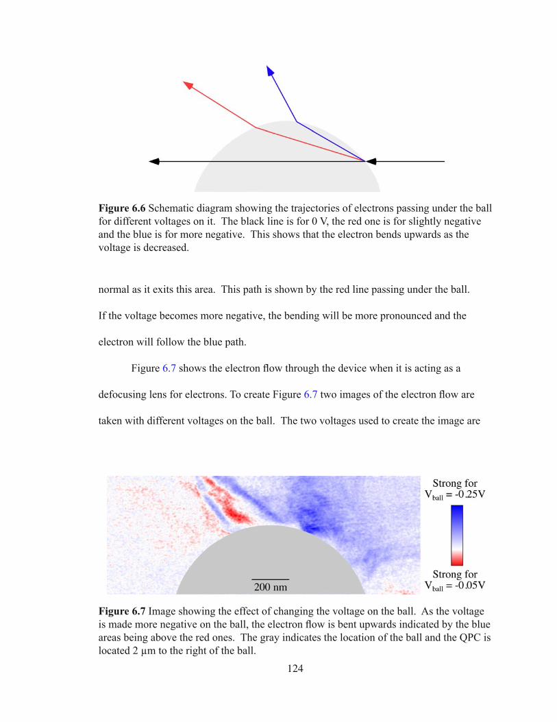
124
normal as it exits this area. This path is shown by the red line passing under the ball.
If the voltage becomes more negative, the bending will be more pronounced and the
electron will follow the blue path.
Figure 6.7 shows the electron flow through the device when it is acting as a
defocusing lens for electrons. To create Figure 6.7 two images of the electron flow are
taken with different voltages on the ball. The two voltages used to create the image are
Figure 6.6 Schematic diagram showing the trajectories of electrons passing under the ball for different voltages on it. The black line is for 0 V, the red one is for slightly negative and the blue is for more negative. This shows that the electron bends upwards as the voltage is decreased.
Figure 6.7 Image showing the effect of changing the voltage on the ball. As the voltage is made more negative on the ball, the electron flow is bent upwards indicated by the blue areas being above the red ones. The gray indicates the location of the ball and the QPC is located 2 µm to the right of the ball.

125
–0.05 V and –0.25 V. The gray area is the outline of the ball, which was not scanned
because the tip is not able to deplete the 2DEG under the metal gate. Then these two
images are subtracted from each other to find the effect of changing the voltage on the
ball. In this image, the areas that are red are stronger for the –0.05 V on the ball while the
blue areas are stronger for –0.25 V on the ball. This shows that making the voltage on the
ball more negative bends the electron trajectories more upwards. This is expected as seen
by the schematic diagram in Figure 6.6.
Figure 6.8 shows the mechanism that creates elliptical shaped interference fringes
when the ball is scattering electron waves. The fringes are created by a two bounce
scattering process where the two bounces are off of the tip and off of the ball. As the tip
is moved the path length for this two bounce path changes. When the phase accumulated
along the path changes by π the interference goes from constructive to destructive. The
location of the ball and QPC are fixed. This means that the line of constant phase is
an ellipse with the ball and QPC as the foci. If the tip moves along this line, the fringe
Figure 6.8 Schematic diagram showing how the elliptical fringes are formed. They are due to a path that goes from the QPC to the ball and then the tip as indicated by the blue lines. The red line shows the line of constant phase for this scattering path.

126
will remain constructive or destructive. However, if the tip is moved off of this line
the accumulated phase will change and the fringe strength will change. This is what
produces the elliptically shaped interference fringes once the ball is fully energized. The
presence of elliptical fringes demonstrates that the interference is caused by a two-bounce
mechanism.
Figure 6.9 is a diagram showing the locations of the images of electron flow used
in this experiment. The red area in front of the ball was imaged to look for the effect of
the ball on the pattern of electron flow. The yellow area above the ball was imaged to
look for the presence of elliptical interference fringes. This area was chosen because
it is away from the electron flow when the ball is not energized but some of the flow is
scatterered into the region when the ball is energized. Elliptical interference fringes in
this area are due to a two-bounce mechanism involving the tip and the ball.
Figure 6.10 shows the electron flow for two voltages on the ball from the red
area in Figure 6.9. In Figure 6.10 (a) the ball is not energized and we are looking at
Figure 6.9 Diagram showing the areas of the images of electron flow. The red box is the area of the images in Figure 6.10. The yellow box is the area for the images in Figure 6.11.
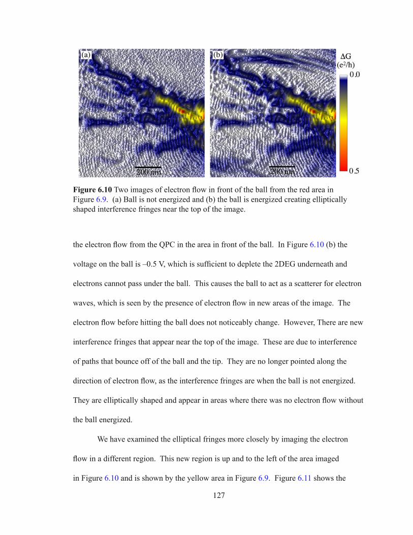
127
the electron flow from the QPC in the area in front of the ball. In Figure 6.10 (b) the
voltage on the ball is –0.5 V, which is sufficient to deplete the 2DEG underneath and
electrons cannot pass under the ball. This causes the ball to act as a scatterer for electron
waves, which is seen by the presence of electron flow in new areas of the image. The
electron flow before hitting the ball does not noticeably change. However, There are new
interference fringes that appear near the top of the image. These are due to interference
of paths that bounce off of the ball and the tip. They are no longer pointed along the
direction of electron flow, as the interference fringes are when the ball is not energized.
They are elliptically shaped and appear in areas where there was no electron flow without
the ball energized.
We have examined the elliptical fringes more closely by imaging the electron
flow in a different region. This new region is up and to the left of the area imaged
in Figure 6.10 and is shown by the yellow area in Figure 6.9. Figure 6.11 shows the
Figure 6.10 Two images of electron flow in front of the ball from the red area in Figure 6.9. (a) Ball is not energized and (b) the ball is energized creating elliptically shaped interference fringes near the top of the image.

128
electron flow for the cases of the ball not energized and energized. We picked a region
where there was little flow without the ball energized since we are only interested in the
elliptical fringes. The presence of electron flow in new areas when the ball is energized
shows that the ball is scattering the flow into these areas. Figure 6.11 (b) shows clear
fringes that are elliptically shaped. The two foci of the ellipses are the QPC and the ball.
This is because the ellipses are created due to a triangular path involving the ball, tip and
QPC. The elliptical fringes demonstrate a new type of interference fringe in our images
caused by a two-bounce scattering mechanism.
In this section, we have presented images of electron flow through a device with
a QPC and a circular gate. We have shown two different uses of the circular electrostatic
gate on the surface. For small voltages on the gate, it acts as a lens for electrons passing
underneath. Once the 2DEG is depleted under the gate, it acts as a scatterer for electron
waves. This causes new interference fringes to form in the images of electron flow.
These new fringes are elliptically shaped since they involve a two-bounce mechanism
Figure 6.11 (a) Image of electron flow without the ball energized from the yellow area in Figure 6.9. (b) Image of electron flow with the ball energized showing the formation of elliptically shaped fringes.
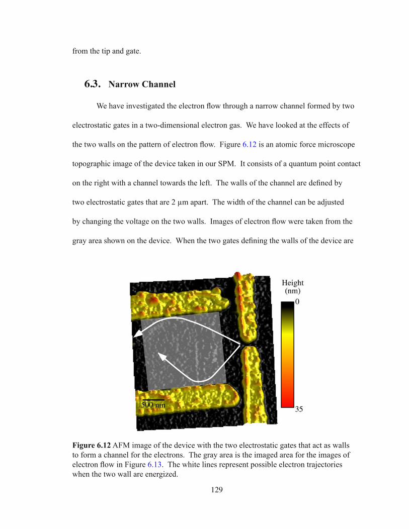
129
from the tip and gate.
6.3. Narrow Channel
We have investigated the electron flow through a narrow channel formed by two
electrostatic gates in a two-dimensional electron gas. We have looked at the effects of
the two walls on the pattern of electron flow. Figure 6.12 is an atomic force microscope
topographic image of the device taken in our SPM. It consists of a quantum point contact
on the right with a channel towards the left. The walls of the channel are defined by
two electrostatic gates that are 2 µm apart. The width of the channel can be adjusted
by changing the voltage on the two walls. Images of electron flow were taken from the
gray area shown on the device. When the two gates defining the walls of the device are
Figure 6.12 AFM image of the device with the two electrostatic gates that act as walls to form a channel for the electrons. The gray area is the imaged area for the images of electron flow in Figure 6.13. The white lines represent possible electron trajectories when the two wall are energized.
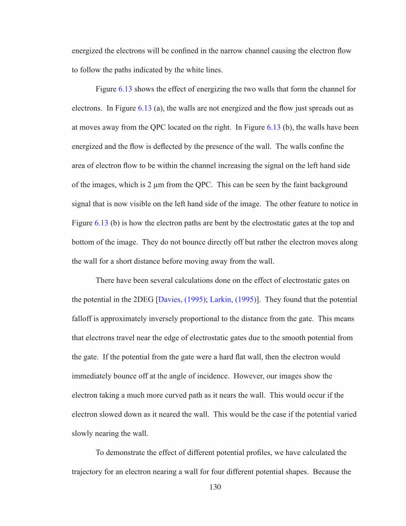
130
energized the electrons will be confined in the narrow channel causing the electron flow
to follow the paths indicated by the white lines.
Figure 6.13 shows the effect of energizing the two walls that form the channel for
electrons. In Figure 6.13 (a), the walls are not energized and the flow just spreads out as
at moves away from the QPC located on the right. In Figure 6.13 (b), the walls have been
energized and the flow is deflected by the presence of the wall. The walls confine the
area of electron flow to be within the channel increasing the signal on the left hand side
of the images, which is 2 µm from the QPC. This can be seen by the faint background
signal that is now visible on the left hand side of the image. The other feature to notice in
Figure 6.13 (b) is how the electron paths are bent by the electrostatic gates at the top and
bottom of the image. They do not bounce directly off but rather the electron moves along
the wall for a short distance before moving away from the wall.
There have been several calculations done on the effect of electrostatic gates on
the potential in the 2DEG [Davies, (1995); Larkin, (1995)]. They found that the potential
falloff is approximately inversely proportional to the distance from the gate. This means
that electrons travel near the edge of electrostatic gates due to the smooth potential from
the gate. If the potential from the gate were a hard flat wall, then the electron would
immediately bounce off at the angle of incidence. However, our images show the
electron taking a much more curved path as it nears the wall. This would occur if the
electron slowed down as it neared the wall. This would be the case if the potential varied
slowly nearing the wall.
To demonstrate the effect of different potential profiles, we have calculated the
trajectory for an electron nearing a wall for four different potential shapes. Because the

131
Fig
ure
6.13
Tw
o im
ages
of
elec
tron
flow
thro
ugh
the
chan
nel d
evic
e fr
om th
e ar
ea in
dica
ted
by th
e gr
ay b
ox in
Fig
ure
6.12
. (a
) T
he
wal
ls o
f th
e ch
anne
l are
not
ene
rgiz
ed a
nd th
e flo
w ju
st s
prea
ds o
ut a
fter
leav
ing
the
QPC
. (b
) The
wal
ls o
f th
e de
vice
are
ene
rgiz
ed,
whi
ch c
onfin
es th
e el
ectr
ons
to th
e na
rrow
cha
nnel
. T
he e
lect
ron
flow
can
be
seen
ben
ding
nea
r th
e bo
ttom
due
to th
e po
tent
ial p
rofil
e of
the
wal
l.
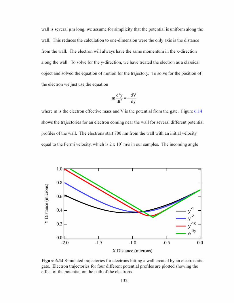
132
wall is several µm long, we assume for simplicity that the potential is uniform along the
wall. This reduces the calculation to one-dimension were the only axis is the distance
from the wall. The electron will always have the same momentum in the x-direction
along the wall. To solve for the y-direction, we have treated the electron as a classical
object and solved the equation of motion for the trajectory. To solve for the position of
the electron we just use the equation
where m is the electron effective mass and V is the potential from the gate. Figure 6.14
shows the trajectories for an electron coming near the wall for several different potential
profiles of the wall. The electrons start 700 nm from the wall with an initial velocity
equal to the Fermi velocity, which is 2 x 10⁵ m/s in our samples. The incoming angle
€
m d2ydt2
= − dVdy
Figure 6.14 Simulated trajectories for electrons hitting a wall created by an electrostatic gate. Electron trajectories for four different potential profiles are plotted showing the effect of the potential on the path of the electrons.

133
of the electron is the same for all of the trajectories and it was chosen to approximate
the angle seen in the images. The four trajectories are for the following potential
profiles for the wall: (black) V(y) ∝ y-1, (blue) V(y) ∝ y-2, (red) V(y) ∝ y-10 and
(green) V(y) ∝ exp(-3y) where y is the distance from the wall in nm. The amplitude
of the potential was chosen so that the electrons turned around when they were 300 nm
from the edge of the wall. As the potential profile changes more quickly, the electron
spends less time near the edge of the wall. In the case of the exponential, the electron is
almost immediately reflected back off of the wall at the same angle as incidence. For the
modeled potential that goes as the inverse of position, it takes more than one µm for the
electron to have its y-momentum fully turned around.
Figure 6.15 shows the image of electron flow with the wall energized. On top
of this image, the trajectory of an electron has been superimposed for the case of the
potential V(y) ∝ y-1. The trajectory is shown by the white curved line near the bottom of
the image. There is fairly good agreement between the lowest branch of electron flow
and this calculated path. This shows that the potential profile is inversely proportional
to the distance from the wall as found in previous calculations [Davies, (1995);
Larkin, (1995)]. If the potentials that change more rapidly are used, the electron bounces
off the wall too quickly and there is not agreement between the measured image and the
simulation.
The addition of two walls can create a channel in which electrons must flow. By
imaging the paths that electrons take through this confined geometry, we have obtained
information on the shape of the potential profile of the walls. We have observed that
the electron spends a long time near the edge of the wall indicating that the potential is

134
slowly varying in this region. A comparison of calculated trajectories with the images
indicates that the potential from the electrostatic gates is inversely proportional to the
distance from the gate. Knowledge of the potential profile from electrostatic gates is
important for the design and simulation of future nanoscale devices,
In this chapter, we have imaged electron flow through several electron-optic
devices to show how they work. These devices can be used as switches, wires and
scatterers for electron waves. The electrostatic prism device changes the direction of
electron flow based on the voltage applied to the gate. The circular ball can be used
Figure 6.15 Comparison of the image of electron flow with a simulated trajectory. The image of electron flow is from the area given by the gray box in Figure 6.12. The white line is the simulated trajectory for a potential profile that is inversely proportional to the distance from the wall. There is good agreement between the simulation and experiment indicating that we can find the potential profile from images of electron flow.

135
either as a defocusing lens or as a circular scatterer. The last device that we have studied
is the narrow channel, which can be used to guide electrons through a 2DEG. These
devices will be necessary for the implementation and integration of devices built in
2DEGs.

136
Chapter 7
Imaging Interference Fringes
This chapter examines the origin of the interference fringes that decorate our
images of electron flow. Section 7.1 discusses the possible origins of these fringes. It
also shows experimental images of the enhancement of the fringes by a small reflecting
gate. In section 7.2, we demonstrate that the location of the interference fringes move
with the position of the reflecting gate. Section 7.3 examines the temperature dependence
of the interference fringes and shows that they are thermally robust near the reflecting
gate.
All of our images of electron flow through a two-dimensional electron gas are
decorated by interference fringes spaced by half the Fermi wavelength. The spacing
of these fringes formed the basis of our measurement of local electron density. In this
chapter, we examine the origin of these fringes and analyze their dependence on distance
from the quantum point contact (QPC). Our images show that the fringes do not decay,
as a function of distance from the QPC for distances up to at least 3 µm, which is much
farther than would be expected with a simple thermal smearing argument. Shaw et al.
[Shaw, (2001)] have proposed that the origin of the fringes is interference of the
backscattered flux from the tip with backscattering from other objects that are near the
same distance from the QPC as the tip. To investigate this mechanism for the robustness
of the fringes, we have fabricated samples with small reflecting arcs at various distances
from the QPC.
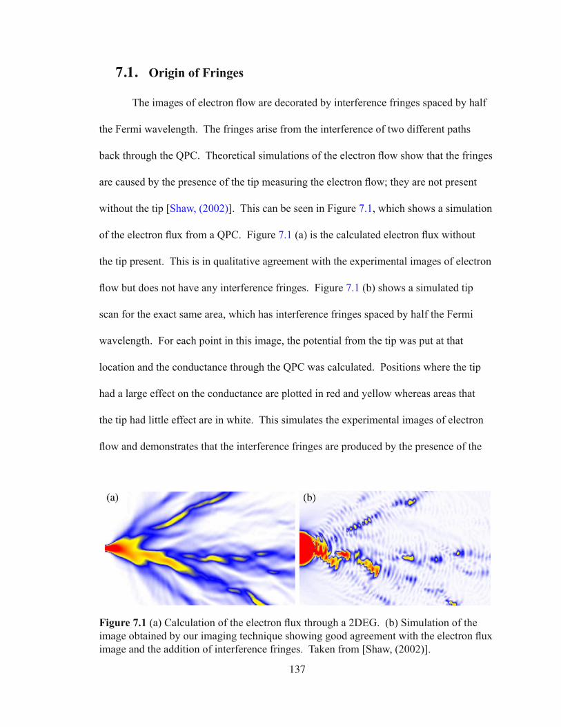
137
7.1. Origin of Fringes
The images of electron flow are decorated by interference fringes spaced by half
the Fermi wavelength. The fringes arise from the interference of two different paths
back through the QPC. Theoretical simulations of the electron flow show that the fringes
are caused by the presence of the tip measuring the electron flow; they are not present
without the tip [Shaw, (2002)]. This can be seen in Figure 7.1, which shows a simulation
of the electron flux from a QPC. Figure 7.1 (a) is the calculated electron flux without
the tip present. This is in qualitative agreement with the experimental images of electron
flow but does not have any interference fringes. Figure 7.1 (b) shows a simulated tip
scan for the exact same area, which has interference fringes spaced by half the Fermi
wavelength. For each point in this image, the potential from the tip was put at that
location and the conductance through the QPC was calculated. Positions where the tip
had a large effect on the conductance are plotted in red and yellow whereas areas that
the tip had little effect are in white. This simulates the experimental images of electron
flow and demonstrates that the interference fringes are produced by the presence of the
Figure 7.1 (a) Calculation of the electron flux through a 2DEG. (b) Simulation of the image obtained by our imaging technique showing good agreement with the electron flux image and the addition of interference fringes. Taken from [Shaw, (2002)].

138
tip. Because the interference fringes are only present with the tip, at least one of the
paths responsible for the interference must involve the tip. The question that we want to
address is what is the other path involved in the interference.
There are several mechanisms that may be responsible for the interference
fringes in our images. To figure out the possible mechanisms that can lead to fringes it is
necessary to identify possible locations where interference can occur. A possible location
for the interference to take place is at the QPC. The next thing to consider is which paths
can interfere to produce a change in the conductance. Because the tip is backscattering
electron flow we must have another path that is going back through the QPC in order to
have interference. A path coming through the QPC has a different value of momentum
and therefore cannot interfere with the backward traveling flux from the tip as long as
the QPC is not tunneling. The simplest mechanism to understand is interference of
multiple paths back to the QPC from the tip. Figure 7.2 illustrates the basic idea behind
this mechanism for producing interference fringes. In this case, one of the paths is the
red one, which goes through the QPC to the tip and straight back through the QPC. The
second path is the red and pink ones, which go from the QPC to the tip then back to the
QPC gate then to the tip and finally back through the QPC. In this case the fringes arise
from interference between a path that makes one roundtrip from the QPC to the tip with
one that makes a roundtrip from the QPC to the tip and from the tip to the gate. The path
length difference between these paths is twice the distance from the gate to the tip so the
fringes would be spaced by half the Fermi wavelength as seen in the images.
Multiple paths backscattering from the tip through QPC seems like a suitable
candidate to explain the fringes seen in the images until the effect of temperature is
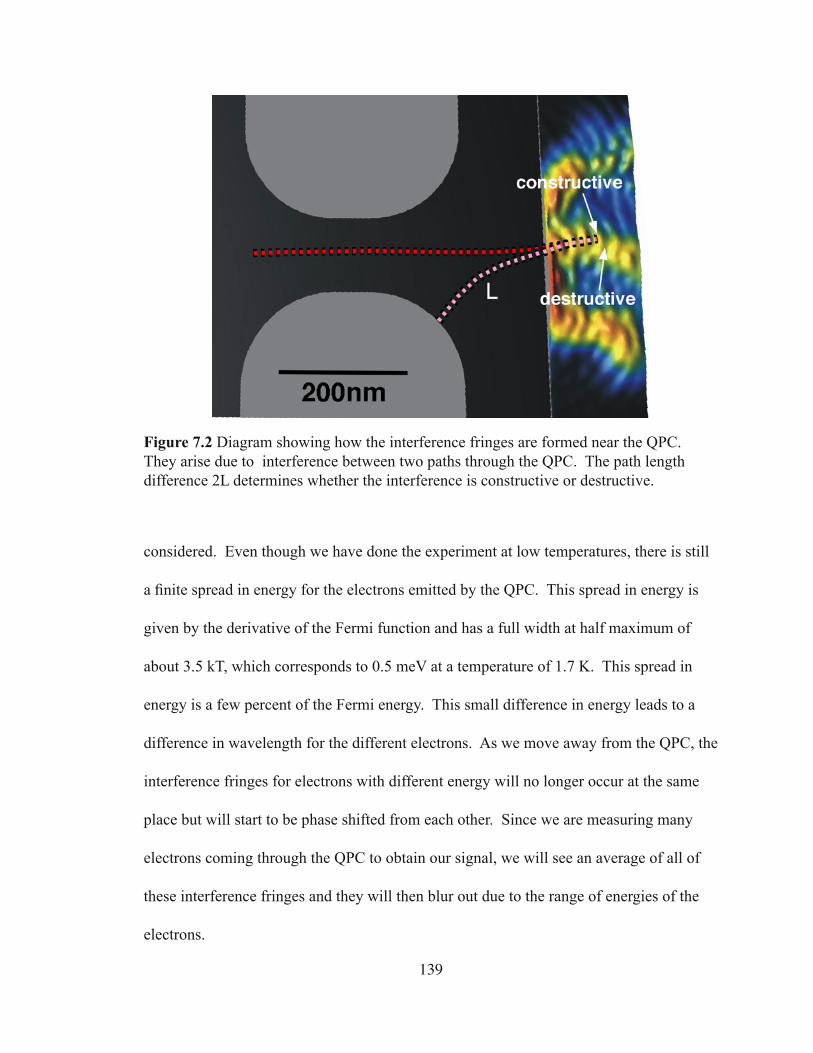
139
considered. Even though we have done the experiment at low temperatures, there is still
a finite spread in energy for the electrons emitted by the QPC. This spread in energy is
given by the derivative of the Fermi function and has a full width at half maximum of
about 3.5 kT, which corresponds to 0.5 meV at a temperature of 1.7 K. This spread in
energy is a few percent of the Fermi energy. This small difference in energy leads to a
difference in wavelength for the different electrons. As we move away from the QPC, the
interference fringes for electrons with different energy will no longer occur at the same
place but will start to be phase shifted from each other. Since we are measuring many
electrons coming through the QPC to obtain our signal, we will see an average of all of
these interference fringes and they will then blur out due to the range of energies of the
electrons.
Figure 7.2 Diagram showing how the interference fringes are formed near the QPC. They arise due to interference between two paths through the QPC. The path length difference 2L determines whether the interference is constructive or destructive.

140
To illustrate the effect of the fringes blurring with increasing distance from the
QPC, we have performed a simple one-dimensional simulation. In this idealized case,
we assume that the potential of both the QPC and tip are delta functions in position and
we calculate the transmission probability through the two of them in series as a function
of the separation between them. Figure 7.3 plots the transmission probability as a
function of distance for three temperatures. At zero temperature, the probability is just
a series of sharp peaks spaced by half the Fermi wavelength indicating the presence of
the interference fringes. As the temperature is raised, the peaks decay in amplitude with
distance with a characteristic decay length given by the temperature. At the temperatures
of the experiments, 1.7 K and 4.2 K, the interference fringes are nearly gone by 500 nm.
As seen from this simple simulation, this mechanism is not enough to explain the
persistence of the fringes with distance from the QPC.
A second mechanism for the fringes has been proposed by Shaw et al.
[Shaw, (2001)]. This second explanation was used because it solved the problem of the
fringes decaying with distance from the QPC. In their theory for the origin of the fringes,
interference takes place between two paths that travel over different areas but have the
same path length. As in any explanation of the fringes one of the paths contributing to
the interference must be from the QPC to the tip and back. In their theory, the second
path is a roundtrip from the QPC to an impurity, which is located roughly the same
distance from the QPC as the tip. The impurity is a located near the same plane as
the 2DEG and therefore creates a sharp peak in the potential, which can backscatter
electrons to the QPC. Clearly, this will produce interference fringes at zero temperature
as the tip is moved due to the phase difference accumulated along these two paths. The

141
Fig
ure
7.3
Tra
nsm
issi
on p
roba
bilit
y th
roug
h a
pote
ntia
l with
two
delta
fun
ctio
ns o
f po
sitio
n as
a f
unct
ion
of th
e di
stan
ce b
etw
een
them
. T
he c
alcu
latio
n is
don
e fo
r th
ree
diff
eren
t tem
pera
ture
s: (
blac
k) 0
K, (
blue
) 1.
7 K
and
(re
d) 4
.2 K
. A
s th
e te
mpe
ratu
re is
in
crea
sed
the
reso
nanc
es d
ecay
as
the
dist
ance
bet
wee
n th
e de
lta f
unct
ions
incr
ease
s. T
his
show
s ho
w th
e in
terf
eren
ce f
ring
es w
ould
de
cay
with
dis
tanc
e.

142
novel feature of this mechanism is what happens to the interference pattern for different
energy electrons. When the tip is at the same distance from the QPC as the impurity,
the path lengths are the same and the interference will be constructive for all energies.
This gives a maximum in the fringes at this location. As the tip is moved away, the
interference fringes for different energies will start to drift out of phase and therefore
their average will slowly decay. However, the impurity has brought all of the fringes in
phase at a particular distance, which is like moving the QPC to this location. Near this
distance from the QPC, the fringes will be strong again. If there are impurities scattered
throughout the sample, then the tip will always be near the same radius as one of the
impurities and the fringes will appear not to decay with distance.
To test this mechanism for producing interference fringes, we have fabricated
a sample that has a reflecting arc located at a fixed distance away from the QPC.
Figure 7.4 shows a schematic diagram of the sample used. The reflecting arc acts like a
large number of impurities all at the same distance from the QPC. We have then taken
images of the electron flow at the same distance from the QPC but in a different area
of the sample as shown by the box in Figure 7.4. If the above theory for the origins
of the fringes is correct, we should expect a strong enhancement of the fringes due
to the presence of the reflecting arc. This is because there will be a large amount of
backscattered flux from the arc that the backscattering from the tip can interfere with.
Figure 7.5 shows the electron flow at the same distance from the QPC as the
reflecting arc for three values of the reflector gate voltage Vrefl
with respect to the
2DEG: (a) Vrefl
= 0 V, (b) Vrefl
= -0.4 V and (c) Vrefl
= -0.8 V. The images were taken at a
temperature of 4.2 K from the area indicated in Figure 7.4, which is located 1500 nm to

143
the right of the QPC and 1300 nm below it. In Figure 7.5 (a), there is no voltage on the
reflector and therefore there is no backscattering from it. Weak interference fringes are
barely visible in this image of the electron flow. In Figure 7.5 (b), Vrefl
is –0.4 V, which
is just enough to deplete under it and enhance the backscattering. There is a marked
Figure 7.5 Three images of electron flow from the area indicated in Figure 7.4 for different voltages on the reflecting arc, (a) 0.0 V, (b) -0.4 V and (c) -0.8 V. When the arc is energized the interference fringes are enhanced due to the increased backscattering from the arc. These images were taken at a temperature of 4.2 K.
Figure 7.4 Schematic diagram showing the layout of the sample used to investigate the persistence of the interference fringes with distance from the QPC. The reflecting arc is shown in the top right side and the scan area is shown in the bottom right. The black dots are impurities located near the plane of the 2DEG.

144
increase in the strength of the interference fringes now that the reflector is backscattering
flux to the QPC. In Figure 7.5 (c), Vrefl
is increased to –0.8 V, which continues to
strengthen the backscattering from the reflector. We continue to see an increase in the
strength of the interference fringes in this third image. These images show that the
addition of a backscattering reflecting arc enhances the interference fringes in our images.
This is true if the images are taken at the same radius as the arc but it does not matter if
the image is actually near the arc, as seen here where the scanned area was almost 2 µm
from the reflecting arc.
To further emphasize the role of the reflecting arc in the enhancement of the
fringes we have performed a two-dimensional FFT on the images of electron flow. The
results of these FFTs are shown in Figure 7.6. The top row, (a-c) is the original data as
Figure 7.6 Images of electron flow for three voltages on the reflecting arc, (a) 0.0 V, (b) -0.4 V, and (c) -0.8 V. (d-f) Fourier transforms of the previous three images showing the enhancement of the interference fringe as the reflector is energized.
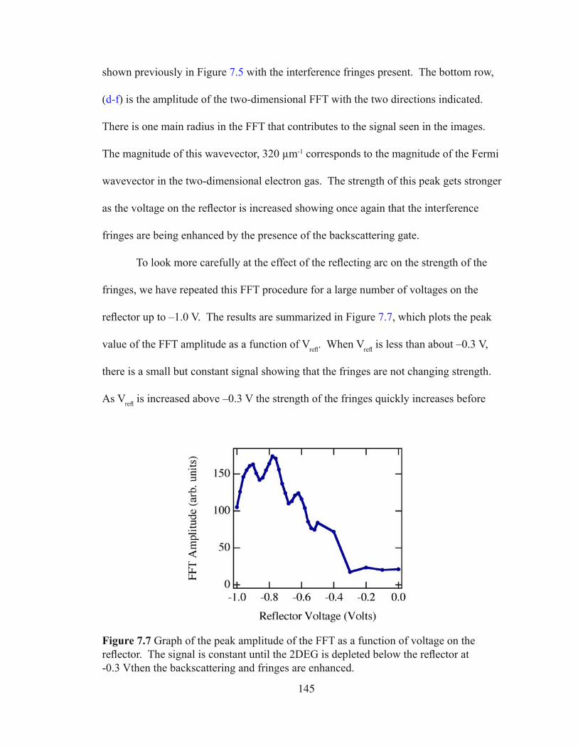
145
shown previously in Figure 7.5 with the interference fringes present. The bottom row,
(d-f) is the amplitude of the two-dimensional FFT with the two directions indicated.
There is one main radius in the FFT that contributes to the signal seen in the images.
The magnitude of this wavevector, 320 µm-1 corresponds to the magnitude of the Fermi
wavevector in the two-dimensional electron gas. The strength of this peak gets stronger
as the voltage on the reflector is increased showing once again that the interference
fringes are being enhanced by the presence of the backscattering gate.
To look more carefully at the effect of the reflecting arc on the strength of the
fringes, we have repeated this FFT procedure for a large number of voltages on the
reflector up to –1.0 V. The results are summarized in Figure 7.7, which plots the peak
value of the FFT amplitude as a function of Vrefl
. When Vrefl
is less than about –0.3 V,
there is a small but constant signal showing that the fringes are not changing strength.
As Vrefl
is increased above –0.3 V the strength of the fringes quickly increases before
Figure 7.7 Graph of the peak amplitude of the FFT as a function of voltage on the reflector. The signal is constant until the 2DEG is depleted below the reflector at -0.3 Vthen the backscattering and fringes are enhanced.

146
slowly leveling off as the voltage continues to be more negative. This sharp increase in
fringe amplitude corresponds to the value of Vrefl
that is necessary to deplete the 2DEG
underneath the gate. This is when the gate first starts to backscatter electrons to the QPC.
The slow increase in the signal beyond this point is due to the size of the reflecting arc
increasing causing an increase in the backscattering and a decrease in the conductance
through the device.
7.2. Fringe movement
In this section, we investigate the movement of the interference fringes as a
function of the position of the reflecting arc. Because the fringes are due to interference
from backscattering from the tip with backscattered paths from the reflecting arc, they
should have a definite phase relation with respect to the position of the arc. When the
tip is at the same distance from the QPC as the front edge of the arc, the signal should
always be constructive since the two backscattered signals will always be in phase. This
implies that the fringes should move as a function of the position of the reflecting arc.
This position can be controlled by changing the voltage on the gate Vrefl
, which makes the
depleted area under the arc grow and therefore the point of backscattering moves closer
to the QPC.
We have investigated the behavior of the fringes as a function of the position of
the reflector by taking repeated scans over the same area for a series of values of Vrefl
.
The scanned area is 1 µm to the left of the QPC and is the same distance from the QPC
as the reflecting arc. The resulting images for five different values of Vrefl
are shown
in Figure 7.8. The circles on the images are guides to the eye so that the positions of

147
the interference fringes can be easily identified. In this series, we have changed Vrefl
by
0.08 V. Moving from (a) to (e) in the images, the guide circles start on the peak of a
fringe and then move slowly to a trough before finally ending on a peak in the last image.
This corresponds to shifting the position of the interference fringes by half the Fermi
wavelength. From a measurement of the conductance through the device as a function
of Vrefl
, the movement of the reflector can be determined [Katine, (1997)]. We have
performed this measurement and found that the movement of the interference fringes
corresponds to the movement of the reflecting arc.
We have repeated this series of images of electron flow at twice the distance of the
Figure 7.8 Images of electron flow 1 µm to the left of the QPC which is the same radius as the reflecting arc. Each image has a different value of V
refl, (a) -0.50 V, (b) -0.52 V,
(c) -0.54 V, (d) -0.56 V and (e) -0.58 V. The circles are guides to the eye showing that the fringes move by half the Fermi wavelength in the five images.
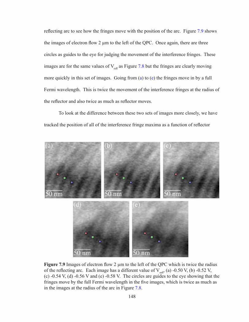
148
reflecting arc to see how the fringes move with the position of the arc. Figure 7.9 shows
the images of electron flow 2 µm to the left of the QPC. Once again, there are three
circles as guides to the eye for judging the movement of the interference fringes. These
images are for the same values of Vrefl
as Figure 7.8 but the fringes are clearly moving
more quickly in this set of images. Going from (a) to (e) the fringes move in by a full
Fermi wavelength. This is twice the movement of the interference fringes at the radius of
the reflector and also twice as much as reflector moves.
To look at the difference between these two sets of images more closely, we have
tracked the position of all of the interference fringe maxima as a function of reflector
Figure 7.9 Images of electron flow 2 µm to the left of the QPC which is twice the radius of the reflecting arc. Each image has a different value of V
refl, (a) -0.50 V, (b) -0.52 V,
(c) -0.54 V, (d) -0.56 V and (e) -0.58 V. The circles are guides to the eye showing that the fringes move by the full Fermi wavelength in the five images, which is twice as much as in the images at the radius of the arc in Figure 7.8.
149
voltage. This was done for a series of 26 values of Vrefl
ranging from -0.5 V to -1.0 V.
The results are shown in Figure 7.10 for the two different distances from the QPC. The
circles in the graphs are the measured peak positions found in the images of electron flow.
The solid lines are linear fits to the peak positions as a function of Vrefl
. The peaks move
much more quickly for the images that are taken at twice the radius of the reflecting arc,
Figure 7.10 (b). The average slope of the peaks for the images at the radius of the arc is
0.10 µm/ Vrefl
while for the images at twice the radius the peak movement is
0.23 µm/ Vrefl
.
The reason for the peaks moving twice as fast at twice the radius of the reflector
can be understood by looking at the mechanism that produces the fringes. Figure 7.11
is a schematic diagram of the fringe mechanism at the two distances. Figure 7.11 (a)
shows the two paths that interfere to produce the fringes at the radius of the reflecting
arc. One of the paths goes from the QPC to the tip and back while the other goes from
the QPC to the reflecting arc and back. These have the same path length causing the
fringes to be enhanced as discussed in the previous section. Because one of the paths
goes from the QPC to the arc and back, a change in the arc position will change the path
length and hence the location of the fringes. Figure 7.11 (b) shows the mechanism for
the interference fringes at twice the radius of the reflecting arc. One of the paths has to
go from the QPC to the tip and back. The second path must have the same path length or
else it will be blurred out due to the finite temperature. The only path that has the same
length is one that goes from the QPC to the arc and back two times. If the position of the
reflecting arc is moved by an amount d, this path length will change by 4d, which is twice
as much as the path involved in the interference at the radius of the arc. Therefore, the
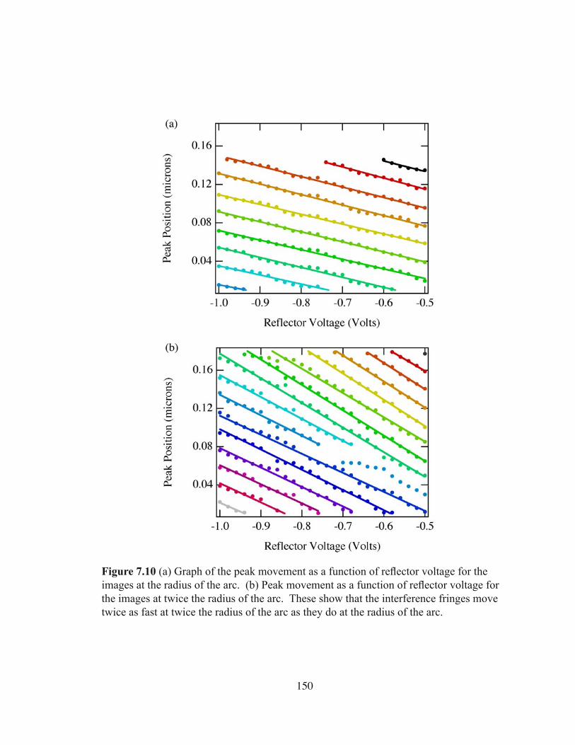
150
Figure 7.10 (a) Graph of the peak movement as a function of reflector voltage for the images at the radius of the arc. (b) Peak movement as a function of reflector voltage for the images at twice the radius of the arc. These show that the interference fringes move twice as fast at twice the radius of the arc as they do at the radius of the arc.
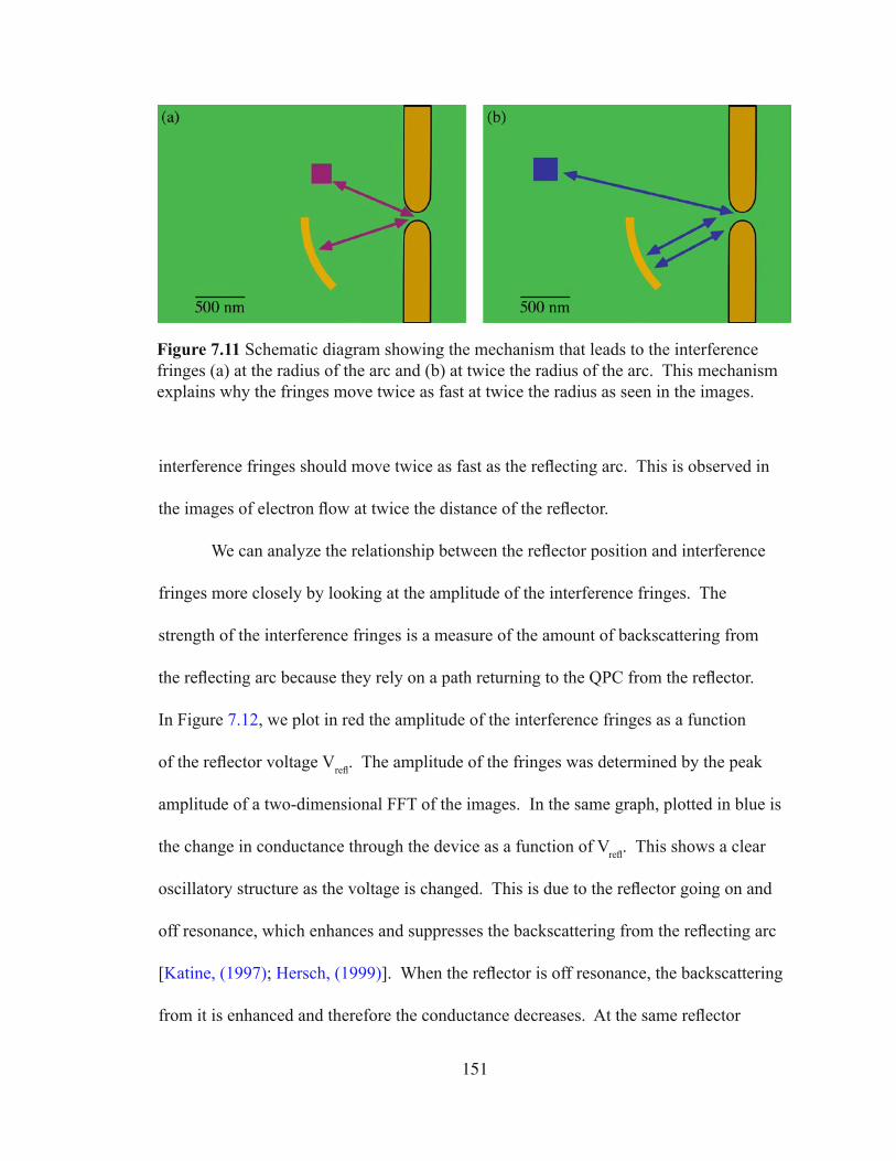
151
interference fringes should move twice as fast as the reflecting arc. This is observed in
the images of electron flow at twice the distance of the reflector.
We can analyze the relationship between the reflector position and interference
fringes more closely by looking at the amplitude of the interference fringes. The
strength of the interference fringes is a measure of the amount of backscattering from
the reflecting arc because they rely on a path returning to the QPC from the reflector.
In Figure 7.12, we plot in red the amplitude of the interference fringes as a function
of the reflector voltage Vrefl
. The amplitude of the fringes was determined by the peak
amplitude of a two-dimensional FFT of the images. In the same graph, plotted in blue is
the change in conductance through the device as a function of Vrefl
. This shows a clear
oscillatory structure as the voltage is changed. This is due to the reflector going on and
off resonance, which enhances and suppresses the backscattering from the reflecting arc
[Katine, (1997); Hersch, (1999)]. When the reflector is off resonance, the backscattering
from it is enhanced and therefore the conductance decreases. At the same reflector
Figure 7.11 Schematic diagram showing the mechanism that leads to the interference fringes (a) at the radius of the arc and (b) at twice the radius of the arc. This mechanism explains why the fringes move twice as fast at twice the radius as seen in the images.

152
voltage, the strength of the interference fringes is enhanced. In contrast, when the
conductance is high through the device the strength of the fringes is suppressed. This
anti-correlation between the conductance of the device and fringe strength is because
when the conductance is high there is less backscattered flux for the signal from the tip
to interfere with. The opposite is the case when the reflector is off resonance and the
conductance is decreased causing an increase in the observed interference fringes.
7.3. Temperature Dependence
To further emphasize the robustness of the fringes, we have looked at the strength
of them near the position of the reflecting arc as a function of temperature. Increasing
Figure 7.12 (Red) Graph of the fringe strength as measured by the peak amplitude of the FFT versus reflector voltage. (Blue) Change in conductance through the device as a function of the voltage on the reflector. There is an anti-correlation between these two signals showing that an enhancement of backscattering from the reflector also enhances the interference fringes in the images.
153
the temperature increases the spread in energy of the electrons that contribute to our
measured signal. This increased spread in energy means that more wavelengths of
electrons contribute to create the interference fringes. At the radius of the arc, there
should be no temperature dependence because there is constructive interference for
all wavelengths and hence energies. As the tip moves away from the arc, the fringes
should only decay weakly with temperature, because the path difference between the
two interfering paths will be small. This small difference in length means that a large
range of wavelengths can be tolerated while still having constructive interference for all
energies. We have simulated a variety of temperatures by applying a voltage across the
QPC to match the energy distribution of electrons at the simulated temperature. Using
an arbitrary function generator, a time varying signal is applied across the QPC. The
voltage from the function generator injects electrons of that energy through the QPC.
The amount of time at any given voltage is given by the probability of the electron having
that energy for the simulated temperature. Therefore, we spend the most amount of time
at 0 V, which corresponds to the Fermi energy and the smallest amount of time at the
highest and lowest voltages, which are the tails of the distribution. As the temperature is
increased the voltage spends more time away from 0 V because there is a larger spread in
energy for the electrons.
Images of electron flow are shown in Figure 7.13 for one real and two
simulated temperatures. Figure 7.13 (a) is a schematic diagram showing the location
of the reflecting arc and the imaged area. Figure 7.13 (b) is at the base temperature
of our experiment, 1.7 K. Figure 7.13 (c) is at a simulated temperature of 4.2 K and
Figure 7.13 (d) is at a simulated temperature of 8.4 K. As the temperature is raised, the

154
Figure 7.13 (a) Schematic diagram showing the location of the images of electron flow. Images of electron flow at three temperatures, (b) 1.7 K, (c) 4.2 K and (d) 8.4 K showing the robustness of the fringes near the radius of the arc. See the text for an explanation of the procedure used to simulate these temperatues. The white line in (b) shows the location of the one-dimensional line sample used in Figure 7.14.

155
relative strength of the fringes near the reflecting arc versus those far away is increasing.
This shows that the fringes at the same location as the reflector are more robust to
increased temperature then those that are away from it. This is what is expected from
the theory, which predicts that the fringes at the position of the reflector will not decrease
with increasing temperature.
We have repeated these images for two more simulated temperatures and then
taken a one-dimensional line sample through all of the images to concentrate on the
amplitude of the fringes as a function of distance from the arc. The location of the one-
dimensional line sample is shown by the white line in Figure 7.13 (b). Figure 7.14 plots
the amplitude of the measured signal as a function of distance for all of the temperatures
Figure 7.14 Graph of the measured signal as a function of the distance from the arc for a series of simulated temperatures. This shows how the strength of the signal decays more quickly away from the arc for increased temperatures but remains robust at the arc position.

156
measured. Each curve has been normalized to its maximum value and offset for clarity.
Once again, it is clear that the interference fringes are decaying as the tip moves away
from the radius of the arc. This decay is more pronounced in the higher temperature
images showing that the presence of the arc is causing the fringes to persist at its radius
even at increased temperatures.
We have used a reflector arc to investigate the origin of the interference fringes in
our images of electron flow. The reflector enhances the fringes in the images at the same
radius from the QPC. The position of the fringes moves with the location of the reflector.
At twice the distance of the reflector, the interference fringes move twice as fast as the
reflector. We have found that the fringes at the same radius as the reflector are robust
against thermal smearing. These results show that the fringes are due to interference
between the backscattered signal from the tip with the backscattered flux from impurities
at nearly the same radius from the QPC as the tip.

157
Chapter 8
Conclusions and Future Directions
In this thesis, we have developed techniques for imaging coherent electron
flow through a two-dimensional electron gas (2DEG). This includes techniques for
measuring the local electron density and characterizing the electron-electron scattering
rate. We have presented images of electron flow through a variety of semiconductor
nanostructures. These images provide more information about the flow of electrons in
a two-dimensional electron gas then is available through the use of standard transport
measurements. The images of electron flow are decorated by interference fringes spaced
by half the Fermi wavelength whose origins are investigated.
We have used these interference fringes to spatially profile the local electron
density. We have varied the density of the 2DEG by using a back gate, which changes
the spacing of the interference fringes. This imaging technique provides information
about the electron density in the 2DEG on a length scale of about 100 nm and can be
used to profile changes in density within a sample. We have also seen how the pattern of
electron flow changes as a function of density. As the density is reduced, the size of the
bumps and dips in the potential due to the donor atoms becomes a larger percentage of
the Fermi energy. This causes the electrons to scatter more quickly and the flow becomes
more diffusive.
We have measured the electron-electron scattering rate as a function of excess
energy added to the electrons. A dc voltage applied across the quantum point contact

158
(QPC) accelerates the electrons as they go through the QPC. The electrons lose
this excess energy through scattering which our imaging technique measures. Our
measurements of the scattering rate in the 2DEG indicate that electron-electron scattering
is the dominant energy loss mechanism in our experiments. This agrees with previous
theoretical and experimental work on scattering in a 2DEG. The previous experiments
required a different sample for each distance measured and were not able to image the
electron flow. Our technique allows the distance and energy dependence of the scattering
to be easily measured in a single sample.
We have also investigated the operation of several electron-optic devices
including a prism, circular scatterer and a narrow channel. The direction of electron flow
can be switched by a voltage applied to the gate of the prism device. We have also shown
how a circular electrostatic gate can scatter electron waves and create new interference
fringes in our images. We have used the narrow channel, defined by two electrostatic
walls, to study the potential profile of a gate on the surface. This shows that the potential
varies slowly as the electron nears the edge of the gate. These experiments show the
operation of electron-optic devices and how a scanning probe microscope can be used to
study them.
In the last part of this thesis we have investigated the origin of the interference
fringes that decorate the images of electron flow. We have found that a small reflecting
arc enhances the fringes in the image at the same radius from the QPC as the arc. The
location of the interference fringes move as the position of the reflector moves. This
shows that the fringes are due to interference from paths backscattering from the tip and
reflecting arc. We have also seen that the strength of the interference fringes is correlated
159
with the amount of backscattering from the arc. This means that a voltage on the
reflecting arc controls the amount of flux traveling through a different part of the sample.
This provides another way to coherently control the flow of electrons through the 2DEG.
The work presented in this thesis opens the way for many new experiments. The
construction of our new He-3 scanning probe microscope lowers the temperature range
that is accessible in our measurements by a factor of 4. This allows new measurements
on electron flow through quantum dots and other closed structures to be performed.
These structures need the lower temperatures for effects like Coulomb blockade and
single electron tunneling. The reduced temperature should also enhance the interference
fringes seen throughout the images. The disappearance of these interference fringes may
provide a novel way to measure the phase coherence length in the 2DEG.
This new scanning probe microscope also includes a magnetic field, which
can be orientated either parallel or perpendicular to the sample. In the perpendicular
orientation, the cyclotron orbits of the electrons can be studied. It is also possible to
look at the pattern of electron flow in the integer and fractional quantum Hall regimes. If
the magnetic field is orientated parallel to the sample, the spin states of the electron are
separated by the Zeeman energy. This allows the investigation of the electron flow for
the two spin states of the electron.
There are also many other systems that can be studied with the scanning probe
microscopes. One of the most promising is InGaAs, which can have a 2DEG formed
very near the surface. This will improve the spatial resolution of our imaging techniques
because the tip can be brought very close to the 2DEG. It also has a much larger g factor
for electrons than GaAs, which enables spin dependant transport to be studied more

160
easily. This is important for the understanding of new spintronic devices that rely on the
electron spin for their operation.

161
References
Adachi, Sadao (1985). “GaAs, AlAs, and AlxGa
1-xAs: Material parameters for use in
research and device applications,” J. Appl. Phys. 58, R1-R29.
Beenakker, C.W.J., and H. van Houten (1991). “Quantum transport in semiconductor nanostructures,” Solid State Physics 44, H. Ehrenreich and D. Turnbull, (eds.), Academic Press, San Diego, CA.
Binnig, G., H. Rohrer, Ch. Gerber, E. Weibel (1982). “Surface studies by scanning tunneling microscopy,” Phys. Rev. Lett. 49, 57.
Binnig, G., C.F. Quate, and Ch. Gerber (1986). “Atomic force microscope,” Phys. Rev. Lett. 56, 930.
Büttiker, M. (1986). “Four-terminal phase-coherent conductance,” Phys. Rev. Lett. 57, 1761.
Chen, L,H. (2001). “Charge-imaging field-effect transistors for scanned probe microscopy,” Ph.D. Thesis, Harvard University.
Ciorga, M, A.S. Sachrajda, P. Hawrylak, C. Gould, P. Zawadzki, S. Jullian, Y. Feng, Z. Wasilewski (2000) “Addition spectrum of a lateral dot from Coulomb and spin-blockade spectroscopy,” Phys. Rev. B 61, R16315.
Crommie, M.F., C.P. Lutz, D.M. Eigler (1993). “Confinement of electrons to quantum corrals on a metal surface,” Science 262, 218.
Crook, R., C.G. Smith, M.Y. Simmons, D.A. Ritchie (2000a). “Imaging diffraction-limited electronic collimation from a non-equilibrium one-dimensional ballistic constriction,” J. Phys.: Condens. Matter 12, L167.
Crook, R., C.G. Smith, M.Y. Simmons, D.A. Ritchie (2000b). “Imaging cyclotron orbits and scattering sites in a high-mobility two-dimensional electron gas,” Phys. Rev. B 62, 5174.
Davies, John H., Ivan A. Larkin, E.V. Sukhorukov (1995). “Modeling the patterned two-dimensional electron gas: Electrostatics,” J. Appl. Phys. 77, 4504.
Davies, John H. (1998). “The physics of low-dimensional semiconductors,” Cambridge University Press, New York, USA.
162
Dingle, R., H.L. Störmer, A.C. Gossard, W. Wiegmann (1978) “Electron mobilities in modulation-doped semiconductor heterojunction superlattices,” Appl. Phys. Lett. 33, 665.
Elzerman, J.M. R. Hanson, J.S. Greidanus, L.H. Willems van Beveren, S. De Franceschi, L.M.K. Vandersypen, S. Tarucha, L.P. Kouwenhoven (2003). “Few-electron quantum dot curcuit with integrated charge read out,” Phys. Rev. B 67, 161308(R).
Eriksson, M.A., R.G. Beck, M. Topinka, J.A. Katine, R.M. Westervelt, K.L. Campman, A.C. Gossard (1996). “Cryogenic scanning probe characterization of semiconductor nanostructures,” Appl. Phys. Lett. 69, 671.
Eriksson, M. A. (1997). “Cryogenic scanning probe microscopy for semiconductor nanostructures,” Ph. D. Thesis, Harvard University.
Finkelstein, G., P.I. Glicofridis, R.C. Ashoori, M. Shayegan (2000). “Topographic mapping of the quantum Hall liquid using a few-electron bubble,” Science 289, 90.
Giuliani, Gabriele F. and John J. Quinn (1982). “Lifetime of a quasiparticle in a two-dimensional electron gas,” Phys. Rev. B 26, 4421.
Harris, J.J., J.A. Pals, and R. Woltjer (1989). “Electronic transport in low-dimensional structures,” Rep. Prog. Phys. 52, 1217.
Heremans, J.J., S. von Molnar, D.D. Awschalom, A.C. Gossard (1999). “Ballistic electron focusing by elliptic reflecting barriers,” Appl. Phys. Lett. 74, 1281.
Herman, M.A. and H. Sitter (1989). “Molecular Beam Epitaxy,” Springer-Verlag, New York.
Hersch, J.S., M.R. Haggerty, E.J. Heller (1999). “Diffractive orbits in an open microwave billiard,” Phys. Rev. Lett. 83, 5342.
Hopkins, P. (1990). “Magnetotransport in wide parabolic GaAs/AlGaAs quantum wells,” Ph. D. Thesis, Harvard University.
Hudson, E. W., S.H. Pan, A.K. Gupta, K.-W. Hg, J.C. Davis (1999). “Atomic-scale quasi-particle scattering resonances in Bi
2Sr
2CaCu
2O
8+δ,” Science 285, 88.
Katine, J. A., (1996). “Electronic quantum interference in ballistic semiconductor nanostructures,” Ph. D. Thesis, Harvard University.
Katine, J.A., M.A. Eriksson, A.S. Adourian, R.M. Westervelt, J.D. Edwards, A. Lupu-Sax, E.J. Heller, K.L. Campman, A.C. Gossard (1997). “Point contact conductance of an open resonator,” Phys. Rev. Lett. 79, 4806.
163
Kouwenhoven, L.P., B.J. van Wees, C.J.P.M. Harmans, J.G. Williamson, H. van Houten, C.W.J. Beenakker, C.T. Foxon, J.J. Harris (1989). “Nonlinear conductance of quantum point contacts,” Phys. Rev. B 39, 8040.
Landauer, R. (1957). “Spatial variation of currents and fields due to localized scatterers in metallic conduction,” IBM J. Res. Dev. 1, 223.
Landauer, R. (1970). “Electrical resistance of disordered one-dimensional lattices,” Phil. Mag. 21, 863.
Larkin, Ivan A., and John H. Davies (1995). “Edge of the two-dimensional electron gas in a gated heterostructure,” Phys. Rev. B 52, R5535.
Lemay, Serge G., Jorg W. Janssen, Michiel van den Hout, Maarten Mooij, Michael J. Bronikowski, Peter A. Willis, Richard Smalley, Leo P. Kouwenhoven, Cees Dekker (2001). “Two-dimensional imaging of electronic wavefunctions in carbon nanotubes,” Nature 412, 617.
Manoharan, H.C., C.P. Lutz, D.M. Eigler (2000). “Quantum mirages formed by coherent projection of electronic structure,” Nature 403, 512.
McCormick, Kent L., Michael T. Woodside, Mike Huang, Mingshaw Wu, Paul L. McEuen, Cem Duruoz, J.S. Harris (1999). “Scanned potential microscopy of edge and bulk currents in the quantum Hall regime,” Phys. Rev. B 59, 4654.
Muller, F., B. Lengeler, Th. Schäpers, J. Appenzeller, A. Förster, Th. Klocke, H. Lüth (1995). “Electron-electron interaction in ballistic electron beams,” Phys Rev B 51, 5099.
Nabity, J. C., and M.N. Wybourne (1989). “A versatile pattern generator for high-resolution electron-beam lithography,” Rev. Sci. Instrum. 60, 27.
Nabity, J. C. (1991). Nanometer Pattern Generation System Manual, Bozeman, MT.
Pan, S.H., E.W. Hudson, K.M. Lang, H. Eisaki, S. Uchida, J.C. Davis (2000). “Imaging the effects of individual zinc impurity atoms on superconductivity in Bi
2Sr
2CaCu
2O
8+δ,”
Nature 403, 746.
Pfeiffer, Loren, K.W. West, H.L. Störmer, K.W. Baldwin (1989). “Electron mobilities exceeding 107 cm2/V s in modulation-doped GaAs,” Appl. Phys. Lett. 55, 1888.
Predel, H., H. Buhmann, L.W. Molenkamp, R.N. Gurzhi, A.N. Kalinenko, A.I. Kopeliovich, A.V. Yanovsky (2000). “Effects of electron-electron scattering on electron-beam propagation in a two-dimensional electron gas,” Phys. Rev. B 62, 2057.
164
Rimberg, A.J. (1992). “Magnetotransport in uniform and modulated electron gases in wide parabolic quantum wells,” Ph.D. Thesis, Harvard University.
Schäpers, Th., M. Krüger, J. Appenzeller, A. Förster, B. Lengeler, H. Lüth (1995). “Effect of electron-electron interaction on hot ballistic electron beams,” Appl. Phys. Lett. 66, 3603.
Shaw, S.E.J., R. Fleischmann, and E.J. Heller (2001). “Quantum coherence beyond the thermal length,” cond-mat/0105354.
Shaw, S.E.J. (2002). “Propagation in smooth random potentials,” Ph.D. Thesis, Harvard University.
Sivan, U., M. Heiblum, C.P. Umbach (1989). “Hot ballistic transport and phonon emission in a two-dimensional electron gas,” Phys. Rev. Lett. 63, 992.
Sivan, U., M. Heiblum, C.P. Umbach, H. Shtrikman (1990). “Electrostatic electron lens in the ballistic regime,” Phys. Rev. B 41, 7937.
Sohn, L.L., L.P. Kouwenhoven and G. Schön (eds) (1997). “Mesoscopic electron transport,” Kluwer Academic, Boston MA.
Spector, J., H.L. Störmer, K.W. Baldwin, L.N. Pfeiffer, K.W. West (1990a). “Control of ballistic electrons in macroscopic two-dimensional electron systems,” Appl. Phys. Lett. 56, 967.
Spector, J., H.L. Störmer, K.W. Baldwin, L.N. Pfeiffer, K.W. West (1990b). “Refractive switch for two-dimensional electrons,” Appl. Phys. Lett. 56, 2433.
Spector, J., H.L. Störmer, K.W. Baldwin, L.N. Pfeiffer, K.W. West (1991). “Noninteracting beams of ballistic two-dimensional electrons,” Appl. Phys. Lett. 58, 263.
Spector, J., J.S. Weiner, H.L. Störmer, K.W. Baldwin, L.N. Pfeiffer, K.W. West (1992). “Ballistic electron optics,” Surface Science 263, 240.
Tarucha, S., D.G. Austing, T. Honda, R.J. van der Hage, L.P. Kouwenhoven (1996). “Shell filling and spin effects in a few electron quantum dot,” Phys. Rev. Lett. 77, 3613.
Tessmer, S.H., P.I. Glicofridis, R.C. Ashoori, L.S. Levitov, M.R. Melloch (1998). “Subsurface charge accumulation imaging of a quantum Hall liquid,” Nature 392, 51.
Topinka, M.A., B.J. LeRoy, S.E.J. Shaw, E.J. Heller, R.M. Westervelt, K.D. Maranowski, A.C. Gossard (2000). “Imaging coherent electron flow from a quantum point contact” Science 289, 2323.

165
Topinka, M.A., B.J. LeRoy, R.M. Westervelt, S.E.J. Shaw, R. Fleischmann, E.J. Heller, K.D. Maranowski, A.C. Gossard (2001). “Coherent branched flow in a two-dimensional electron gas” Nature 410, 183.
Topinka, M. A. (2002). “Imaging coherent electron wave flow through 2-D electron gas nanostructures,” Ph.D. Thesis, Harvard University.
van Wees, B.J., H. van Houten, C.W.J. Beenakker, J.G. Williamson, L.P. Kouwenhoven, D. van der Marel, and C.T. Foxon (1988). “Quantized conductance of point contacts in a two-dimensional electron gas,” Phys. Rev. Lett. 60, 848.
Wharam, D.A., T.J. Thornton, R. Newbury, M. Pepper, H. Ahmed, J.E.F. Frost, D.G. Hasko, D.C. Peacock, D.A. Ritchie, and G.A.C. Jones (1988). “One-dimensional transport and the quantization of the ballistic resistance,” J. Phys. C: Solid State Phys. 21, L209-L214.
Woodside, Michael T. and Paul L. McEuen (2002). “Scanned probe imaging of single-electron charge states in nanotube quantum dots,” Science 296, 1098.
Yacoby, A., U. Sivan, C.P. Umbach, J.M. Hong (1991). “Interference and dephasing by electron-electron interaction on length scales shorter than the elastic mean free path,” Phys. Rev. Lett. 66, 1938.
Yacoby, A., H.F. Hess, T.A. Fulton, L.N. Pfeiffer, K.W. West (1999). “Electrical imaging of the quantum Hall state,” Solid State Comm. 111, 1.

166
Appendix
A. SEM Procedure
This section details the procedure that is used for writing ohmics and devices
on the JEOL SEM. It is divided into six sections, loading a sample, imaging, focusing,
writing, changing samples and shutting down.
A.1. Loading Sample
a. Put the sample into the sample holder and screw it onto the end of the manipulator.
b. Pump out the airlock by pushing the red button.
c. Make sure that the Nitrogen cold trap is full.
c. Check that the detector is off in the EOS menu.
d. Load the correct setup from Memory. We use a working distance of 15 mm and an accelerating voltage of 35 kV.
e. Put the sample all the way in and check that it is securely in place. Unscrew the rod and pull it out. Close the airlock and vent it by pushing the red button again.
A.2. Initial Images
a. Move the sample away at least 7 mm in some direction. This ensures that you will not expose the sample by accident.
b. Change the working distance with the big knob to 15 mm.
c. Check that the magnification is 500.
d. Turn on the accelerating voltage.
e. Switch to fast, line mode with the maximum contrast.

167
f. Slowly turn up the current. It should take about 1 minute to turn up the current. The signal on the screen should go up then down and back up again before hitting a plateau. Turn down the current so that it is just below this plateau.
g. Switch to the picture mode and find your chips.
A.3. Aligning and Focusing
a. Get a rough focus on one of the corners of the chip.
b. Change the mode to the one with the crosshairs and make sure that the image zooms in on them. If it does not you have to adjust their position in the EOS menu.
c. Adjust the mechanical rotation so that when you move in the x direction you go from the top right to the top left of the chip.
d. Adjust the scan rotation so that image moves straight across the screen.
e. If only writing large features find the focus on two opposite corners of the chip and set the value to the average of these.
f. If writing fine features focus on the silver paint on the four sides of the sample. Adjust the astigmatism at the first silver paint location. Fit a plane to these four values of the focus to determine the appropriate focus for the device location.
A.4. Writing
a. Turn the contrast and brightness all the way down.
b. Switch the beam blanking to external.
c. Switch to slow mode.
d. Switch to computer control using the Pomona box.
e. Turn up the brightness until the dot appears at the center of the screen. This should be about 220.
f. Adjust the tilt and shift to maximize the current. The tilt should be adjusted on condenser lens 16 and the shift on condenser lens 1. I usually do this into the PCD cup but it can also be done into the hole on the sample holder. I find the only thing that really matters is that you consistently use one or the other because they give different readings

168
of the current, which can affect the writing of the pattern.
g. Move to the position for the device.
h. Set up the run file for the pattern. This is done with the command “mrf filename” were filename is the name of the file to write.
i. Set the magnification and condenser lens for the first layer.
j. Run the command “pg filename” where filename is the name of the file that you are writing.
k. Continue setting the magnification and current until all the layers are written.
A.5. JEOL Control
a. Move away from the chip and turn the current down to condenser lens 16.
b. Make sure the magnification is above 100 and the PCD cup is in.
c. Turn the brightness down to zero to avoid a bright spot showing up on the screen.
d. Switch the Pomona box back to JEOL control and switch back to fast mode.
e. Turn up the contrast and brightness. Remove the PCD cup to go back to the imaging mode.
A.6. Shut Down
a. Slowly turn down the current.
b. Turn off the accelerating voltage.
c. Check that the detector is off in the EOS-3 menu.
d. Move the sample back to the exchange position. Set the working distance to 39 mm and the rotation back to zero. Then remove the sample using the same procedure as putting it in.
e. Set the magnification to the maximum value, 300,000, go to slow picture mode. Make sure that the beam blanking is off, the PCD cup is out and the scan rotation is off.

169
f. Get rid of the writing on the screen using the PF1 key.
B. Script Commands
This section lists all of the commands that can be used in the script window of
the AFM program. They are broken down into subsections relating to scans, sweeps,
graphics, utilities, movies, simulations and several others.
B.1. Utility Commands
These are basic utility commands used in the program. Most of the variables
that can be set in the dashboard are also available in these commands. They set internal
variables like how long to wait when finding the surface, the working directory, and the
conversion factor from voltage to conductance.
af.drift [drift (Volts)] The amount of drift in the cantilever signal when doing the autoflatten routine.
af.pause [wait (secs)] The amount of time to wait between points when doing the autoflatten routine.
atan [x] [y]Calculates the arctan(y/x).
constantstep [# of bits] Sets distance between pixels in scan to be the given number of bits.
debugout.start [outCh] Prints the values being sent to the given channel in the sweep window.
debugout.end Turns off the output printing in the sweep window.
decfnumDecreases the current file number by one.

170
decimal [number] Prints the decimal portion of the number.
delay [time (secs)] Waits the specified time before doing the next command.
dialog [str0] [str1] [str2] [str3]Creates a dialog box with the strings in it.
feedbackreturn [straight/cw/ccw] [margin (Volts)] Determines which way the tip moves back to the origin after finishing a scan.
Straight is the default type. It can also move either clockwise or counterclockwise. Margin determines the distance in volts outside of the current scan area that the tip moves. This is only used for cw and ccw. The default value is 1.
filecomment= [comment0] [comment1] Sets the file comment that is saved with the scan, can be seen using the get info
command in the Finder. This does not work in OS X because comments are no longer supported by the operating system.
floor [number] Prints the integer portion of the number.
fs.downtime [time (secs)] How long to sit on the surface when running FindSurface, default is 0.2s.
fs.offheight [height (Volts)] How far off the surface to move when running FindSurface, default is 0.5V.
fs.tau [tau (secs)] How long to take moving to the surface when running FindSurface, default is 0.01s.
fs.uptime [time (secs)] How long to sit off the surface when running FindSurface, default is 0.02s.
graphinchan [graph: a-d] [ch] Sets the channels to read into the given graph.
graphonoff [graph: a-d] [on/off] Turn on or off the reading into the given graph.
help [command] Find help on the given command.

171
incfnumIncreases the current file number by one.
makesafe Sets the gate, reflector and tip voltage to zero.
movecursors [cursor: r,g,b] [x] [y] [cursor: r,g,b] [x] [y] [cursor: r,g,b] [x] [y] Moves the indicated cursors to the specified location.
print [string0] [string1] [string2] etc. Prints the given string(s) to the console window.
printfilecommentPrints the current file comment in the console window.
printscanstats [graph: a-d] Prints the stats associated with the given graph to the console window. These stats
currently include the size of the image, the speed, the direction of the scan and the settings of the output voltages.
printscanval [graph: a-d] [x] [y] Prints in the console window the value at point (x,y) in the specified graph. The value
of x and y are the voltage values.
setanalysisradius [radius (pixels)] Sets the radius to use in calculating a sweep from a collection of slides, default is 1.
setdigital [a0/a1/a2/a3/b0/b1/b2/b3] [0/1] Sets one of the eight digital output to either 0 or 1.
setdioout [upper] [lower] Toggles the dio output between the upper+lower and 0.
setdir [directory] Sets the directory for saving files.
setfastdir [l2r/r2l/b2t/t2b] Sets the fast scan direction. There are four choices: Right to Left, Left to Right,
Bottom to Top, or Top to Bottom.
setfeedback [setpoint] Sets the feedback to the desired setpoint.
setflyback [speed (V/s)] Sets the speed for the flyback.
172
setfnum [#] Sets the current file number.
setgateExtra [Extra (Volts)] The amount to pull off the surface when over a gate as defined by setgatethreshold.
setgatethreshold [Thresh (Volts)] Used to define the area in a scan that is over the gate, when using the z-guide.
setgatev [voltage] Sets the gate voltage.
setheight [Height (Volts)] [Drift (Volts)] Finds the surface and then pulls away by the amount in height. Drift sets the average
drift on the cantilever in order to make sure that we find the real surface.
sethover Moves the tip 0.5V off of the surface. There must be a zguide to run this.
setnpts [# of pts]Sets the number of points in the scan.
setpixelbuffer [# of pixels] Sets the buffer around the edge of gates. This is used when making a z-guide to give
an extra margin of safety.
setreflv [Volts] Sets the reflector voltage.
setscanrot [angle] [opt: ok] Rotates the scan to the given angle. Option ok moves the tip without a warning.
setslowdir [l2r/r2l/b2t/t2b] Sets the slow scan direction. There are four choices: Right to Left, Left to Right,
Bottom to Top, or Top to Bottom.
setsweepio [inCh] [mio16x/ao6] [outCh] Sets the I/O parameters for a sweep. Lets you specifiy the input channel on the MIO
and also the output channel on either the MIO or AO.
setsweeprange [start] [end] [step] [reads per point] Sets the starting and ending voltage values for a sweep. Also sets the step size and
the number of reads to do per point.

173
settau [tau (secs)] Sets the slow down time used in smooth scans.
settempparams [alarm delta] [vShift_He] [vShift_N] Changes the calibration settings for the thermometers.
settipspeed [V/s] Sets the scanning speed.
settipv [Volts] Sets the tip voltage.
setvbuffer [buffer (Volts)] Extra amount to be off the surface for all points on a z-guide.
setvoltconv [ao6/mio16x/tip/gate/refl] [ch#] [Voffset] [Vmult] Changes the multiplier. If tip/gate/refl is specified then ch# can be left blank. The
actual voltage put onto the sample is Vreal = Voffset +(Vcomp * Vmult)
setvout [mio16x/ao6/dio] [Ch] [volts] A more general output setting call. Lets you specify the board and also the channel
that you want the voltage to be set on.
setxchannel [ch] Changes the channel that is the x axis of the scans.
setxmultiplier [mult] Changes the multiplier for the output to the x axis.
setxyrot [xCh] [yCh] [angle]Changes the x and y channel along with the scan rotation.
setychannel [ch] Changes the channel that is the y axis of the scans.
setymultiplier [mult] Changes the multiplier for the output to the y axis.
setzv [Volts] Sets the voltage to the z piezo. This controls the height of the tip off the surface.
smoothscan [on/off] Whether or not to do smooth scans.

174
squarepixels [on/off] Whether or not the pixels in a scan have to be square.
temps2sweep Takes the data from the temperature plot and moves it into the sweep window.
unstickv= [Volts] Sets the amount of volts the tip pulls off the surface with the unstick tip command.
userpause.off Turns off the pausing.
userpause.on Turns on a pause that requires the user to hit a key to continue.
v124tog.on Turns on the conversion from the PAR124 to G values for sweeps.
v124tog.off Turns off the conversion from the PAR124 to G values for sweeps.
v124togparams [V10k] [Rseries] [Gmax] [Vzero] Sets the parameters necessary to convert the output of the PAR124 into G values.
v124togvalue [value] Converts value into a G value using the parameters stored in v124togparams.
vguide [on/off] Turns the vguide on or off.
zguide [on/off] Turns the zguide on or off.
B.2. Graphics Commands
These commands are all related to the graphics display in the program. There
is a set of commands for displaying the data in 3D including the placement of lights for
highlighting it. There are also a set of commands for setting the color scale, location and
other parameters of the image.

175
3d.backcolor [r] [g] [b] Sets the color of the background.
3d.eye [x] [y] [z] Sets the eye position.
3d.fieldofview [angle (deg)] Sets the angle for the field of view.
3d.focus [auto, x] [y] [z] Sets the focus point. If the first parameter is auto, then the focus is the center of the
data. Otherwise, the focus is set to the position given.
3d.geteye Prints the position of the eye in the script window.
3d.glarefactor [factor] Sets the glare factor.
3d.glarewidth [width (deg)] Sets the width of the glare in degrees.
3d.grid [dx (pixels)] [dy (pixels)] Places a grid on the data with the given spacing in x and y.
3d.light [number] [x] [y] [z] [r] [g] [b] [ambient/non] [width] Adds a light. Number is the light number to add. (Use 0 for ambient). The position
of the light is given by x,y,z and its color is given by r,g,b. The width of the light is given by width.
3d.off [graph: a-d] Turns off 3D for the given graph.
3d.on [graph: a-d] Turns on 3D for the given graph.
3d.polyarc [x] [y] [z] [radius] [StartAngle] [EndAngle] [NumPts] Creates an arc. x,y,z gives the center coordinates of the arc. The radius is given by
radius and the starting and ending points are given by StartAngle and EndAngle. Creates the arc by dividing it into NumPts straight lines.
3d.polyclear [graph: a-d] Clears all the polygons in a given graph.

176
3d.polyend Ends the polygon by drawing a line from the last point defined to the starting point.
3d.polyline [x] [y] [z] Draws a line from the previous point defined to the point given by x,y,z.
3d.polystart [graph: a-d] [r] [g] [b] [x] [y] [z] Starts a polygon in the given graph. The color of the ploygon is determined by r,g,b
and the first point is given by x,y,z.
3d.removelight [number] Removes the light given by number. Also shifts the numbers of all the other lights.
3d.scale [xScale] [yScale] [zScale] Changes the scale.
3d.scalefactor [factor]Changes the scale by a factor.
3d.sidecolor [r] [g] [b] Sets the color of objects that have cMarker0_f64 as one of their points.
3d.viewangle [angle (deg)] Sets the viewing angle in degrees.
autoxy [graph: a-d] Automatically changes the range on the specified graph to include all of the data.
autoz [graph: a-d] Sets the color scale so that all of the data is within the scale.
backcolor [r] [g] [b] Sets the background color of all the graphs.
bandsoff [graph: a-d] Turns off the display of the bands.
bandson [graph: a-d] [base] [width] [spacing] [exclude] [r] [g] [b] [weight] [ave/add] Puts color bands on the data in the graph. The width, spacing and color are controlled
by the parameters.

177
colorscheme [graph: a-d] [scheme] Sets the color scheme for the selected graph. The scheme must include special0 and
then one of the following schemes blackbottom, halloween, sand&water, water&sand, ice&fire, fire&ice, emerald&sapphire or sapphire&emerald. You can also specify where to take the average value. The choices are bottom, top, right or left. There are also two other options maxmid() and minmid().
copycolors [graph1: a-d] [graph2: a-d] Copies the colors from graph1 into graph2. This does not change the colors stored in
the data for graph2. To do this, use the command storecolors.
copygraph [graph: a-d] [Width (pixels)] [Height (pix)] or [Magnification (x1,x2)] Copys the specified graph into a new window so that it is available to other programs.
copygraph.raytrace [graph: a-d] [density] Same as copygraph except lines are drawn for the prism data.
depixel [graph: a-d] Sets the graph limits so that one screen pixel is one data pixel.
drawellipse [graph: a-d] Draws an ellipse in the given graph. The red and green cursor are at the foci, the blue
is at a point on the ellipse.
drawellipse [graph: a-d] [focus1x] [focus1y] [focus2x] [focus2y] [xPt] [yPt] Draws an ellipse on the graph with the given foci and a point on the ellipse.
getcolors [graph: a-d] Prints the colors of the specified graph into the script window.
line.clear [num] Clears the specified line.
line.clearall Clears all of the lines.
line.get [num] Prints the coordinates of the line in the script window.
line.make [num] [pt1x (Volts)] [pt1y (Volts)] [pt2x] [pt2y] etc. Draw a line on the graphs through the given points.
line.move [num] Moves the start of the line to the blue cursor.

178
line.slice [graph: a-d] [num Cuts] Take cuts perpendicular to the lines in the given graph, display in the sweep window.
line.start [num] Clears the line information so that it can be started.
outlinegate [graph: a-d] [sign] [thresh] [r] [g] [b] [rWeight] [gWeight] [bWeight] Draws a line of color rgb around the area that is a gate defined by thresh and sign.
plots.on Turns plotting of scans on.
plots.off Turns plotting of scans off.
restorecolors [graph: a-d] Restores the colors that are saved with the data for the specified graph.
resizewindow [window] [top (pixels)] [left] [width] [height] Resizes the given window.
setcolors [graph: a-d] [value1] [r1] [g1] [b1] [rgb/hsv/hsl] [value2] [r2] [g2] [b2] etc Sets the colors on the color bar. Value gives the value on the color bar and r,g,b gives
the color at that point. Then rgb/hsv/hsl gives the method to go to the next value.
setgraphsigfigs [graph: a-d] [# sigFigs] Changes the number of significant figures displayed on the colorbar and scan range
for the given graph.
setgraphxy [graph: a-d] [xStart] [yStart] [xEnd] [yEnd] Changes the range on the specified graph to be from xStart to xEnd and yStart to
yEnd.
setgraphz [graph: a-d] [min (Volts)] [max] or [graph: a-d] [type] [range] Sets the range of the color scale on the graph
shiftcolorstop [graph: a-d] [cStop] [newV (Volts)] Shifts the color stop to the new voltage.
storecolors [graph: a-d] Stores the colors of the specified graph in the data.
supimpgate [graph: a-d] [sign] [thresh] [r] [g] [b] [rWeight] [gWeight] [bWeight] Superimposes the gate on the other graphs. Puts everything above thresh in graph
onto the other graphs with the given color. Call with no parameters, to turn off.

179
waveplot.off Turns off plotting of phase information.
waveplot.on Plots phase information from graph d onto data in graph a.
zoomin [graph: a-d] Zooms in on the cursors in the given graph.
B.3. Scan Commands
These commands all manipulate scan data. There are also commands, which are
used for data analysis on the scans. These commands are mostly used when looking at a
scan after acquiring it.
scan.addsweep [graph: a-d] [sweepNum] [x] Adds a sweep as a column at the given x position in the graph.
scan.approxmedians [graphFrom: a-d] [graphTo: a-d] [percentile] [bins] [radius] Approximates the given percentile in a radius around each point in the scan.
scan.autoshiftdata [graph1: a-d] [graph2: a-d] [dx] [dy] [opt: c] The program shifts graph1 to try to match graph2. If parameter 5 is c, then the area of
interest is just between the cursors, otherwise the entire scan is used.
scan.arcsample [graph: a-d] [nBins] [start angle] [end angle] [center angle] [datainc] Takes a sample of the given graph in an arc shape. The blue cursor defines the center
of the arc. The red and green cursors give the inner and outer radii.
scan.average [graph1: a-d] [graph2: a-d] [weight] Takes the average of graph1 and graph2 with weight given to graph1.
Graph1 = (weight*graph1 + graph2)/(weight+1).
scan.chop [graph: a-d] [min (Volts)] [max (Volts)] Chops off the values of the scan that lie outside of min and max.
scan.circpeakfind [graph: a-d] [radius step] [sign] [excl: startang] [excl: endang] Finds the peak in the circular slice. The area from startang to endang is excluded
in the search. If sign is 1 finds the maximum, -1 finds the minimum and 0 finds the average. The red cursor defines the center of the circle.

180
scan.circpeakfind2 [graph: a-d] [radius step] [sign] [fraction] Finds the peak in the circular slice. The analysis only looks at fraction of the scan. If
sign is 1 finds the maximum, -1 finds the minimum and 0 finds the average. The red cursor defines the center of the circle.
scan.clear [graph: a-d] Clears the specified graph.
scan.combinescan [graph1: a-d] [graph2: a-d] [spacer] Puts two scans together with spacer pixels between them in the x direction.
scan.constant [graph: a-d] [value] Puts a scan of constant value into the specified graph.
scan.contourfillin [graph: a-d] [smooth1] [skew1] [smooth2] [skew2] [smooth3] [skew3] opt: storeguide()
Smooths the data to eliminate the high frequency components. The skew parameters are used to set the weight for the x direction as compared to the y direction.
scan.copyintofrom [graphIn: a-d] [graphFrom: a-d] Copies the scan from graphFrom into graphIn.
scan.crop [graph: a-d] [left (pixels)] [top] [right] [bottom], opt: cursors Crops some of the scan in graph based on the values in left, top, right, and bottom. If
the option cursors is selected the scan is cropped using the boundary of the cursors.
scan.crop.multipleof [graph: a-d] [number] Crops the scan so that the number of pixels in each direction is a multiple of number.
scan.cutoffpeaks [graph: a-d] Calculates the average between the cursors and also the minimum value. Then sets
all peaks greater than (average+minimum)/2 to the average.
scan.destreak [graph: a-d] [threshold] Attempts to remove jumps in the graph greater than threshold by adjusting the values.
scan.disttopeak [graph: a-d] Uses the red and green cursors to define an area of the scan and then calculates the
distance from the origin to the peak in this area.
scan.difference [graph1: a-d] [graph2: a-d] Takes graph1 and subtracts graph2, puts the result in graph1.
scan.divide [graph1: a-d] [graph2: a-d] Divides graph1 by graph2 and puts the result in graph1.

181
scan.dy [graph: a-d] Calculates the differential in the y direction by multiplying the difference between
two adjacent sets of data.
scan.enforcemirror [graph: a-d] [yMirror (pixels)] Mirrors the data across the horizontal line given by yMirror.
scan.fft [graphIn: a-d] [graphOut: a-d] Takes the fft of graphIn and puts it into graphOut. Must have 2Nx2M pixels.
scan.fillin [graph: a-d] [# of fills] Fills in the graph by raising any point that is lower than its neighbors.
scan.fillintofrom [graph1: a-d] [graph2: a-d] Fills in the graph1 by raising any point that is lower than the corresponding region in
graph2.
scan.filter [graph: a-d] [FilterType (number)] [freq1] [freq2] Filters the scan using a FFT. The possible filter types are a high pass filter (1), a low
pass filter (2), a notch filter (3), filter near x=0 (4) and filter near y=0 (5). The last two parameters set the relevant frequencies in the filter.
scan.findmedians [graphFrom: a-d] [graphInto: a-d] [radius (pixels)] Finds the local median in graphFrom using the radius and puts the result in graphInto.
scan.findplateau [graph: a-d] [start] [end] [range] [wght] [grphX: a-d] [grphY: a-d] Looks for plateaus starting with graph+start and going to graph+end. Once a plateau
is found calculates the value of it by averaging points within range of it using weight. Then stores the value in graphX or graphY.
scan.flipl2r [graph: a-d] Flips the graph from left to right.
scan.getvalue [graph: a-d] [x (pixels)] [y (pixels)] Prints in the console window the value at point (x,y) in the specified graph.
scan.gradient [graph: a-d] Takes the gradient squared of the given scan.
scan.levelize [graph: a-d] Takes the average in the x direction between the red and green cursors. Then
computes the average over each line between the cursors. The difference between these two averages is added to all of the data in the line.
182
scan.linesample [graph: a-d] [nBins] [radius (pixels)] [microns per volt] Takes a sample of the data between the red and green cursors, displays in sweep.
scan.linestack [graph: a-d] Turns each line in the graph into a sweep.
scan.ln [graph: a-d] Takes the natural log of the scan.
scan.load [graph: a-d] [fname] [fname add-on] etc Loads the scan into the graph.
scan.localmedian [graph: a-d] [x (pixel)] [y (pixel)] [radius (pixels)] Finds the local median at the point (x,y) using radius to define the region.
scan.makesinewave [graph: a-d] [amplitude (volts)] [period (volts)] [angle] [opt: Nx] [opt: Ny] [xWidth (volts)] [yWidth (volts)]
Creates a scan with a sine wave of the given parameters in it. The optional parameters set the total number of points in the scan and the area of it.
scan.match [graph1: a-d] [graph2: a-d] Takes graph1 - # graph2 and puts it into graph1. The routine attempts to minimize the
least squares difference in the two scans.
scan.minusconstant [graph: a-d] [constant] Subtracts a constant value from the scan.
scan.normalize [graph: a-d] Normalizes the scan so all of the values lie between 0 and 1.
scan.padwithzeros [graph: a-d] [numX (pixels)] [numY (pixels)] Pads the scan with zeros so that it has the given total number of pixels in X and Y.
scan.percentilelevelize [graph: a-d] [perc Base] [perc Line] opt: multRemoves jumps in the data between the red and green cursors that are caused by charging events. Makes the value of the percentile of each line equal to the value of the percentile of the base scan.
scan.plusconstant [graph: a-d] [constant]Adds the constant to the scan.
scan.polishsurface [graph: a-d] [surfaceWiggle] Anything that is smaller in magnitude than surface wiggle is made constant.
183
scan.psd [graph: a-d] [max freq] Calculates the power spectrum of a scan.
scan.radialintegrate [graph: a-d] [nBins] [startAng] [endAng] opt: !total, !oversample(), !weight(x^2), !weight(x^4)
Performs a radial integration of the data in the graph. The integration goes from the red to the green cursors and is divided into bins. The data from the strating to the ending angle is averaged. The options allow the total signal to be given, different weights for the distances and also oversampling of the graph.
scan.radialmarkpercentile [graph: a-d] [bins] [ang0] [ang1] [percentile] opt: keep+, total
Basically the same as scan.radialpercentile but uses a different algorithm to find the percentile, which may speed up the execution of the command.
scan.radialmode [graph: a-d] [nBins] [ang0] [ang1] [nSubBins] Calculates the mode in the region bounded by the two angles and the red and green
cursors.
scan.radialpercentile [graph: a-d] [bins] [ang0] [ang1] [percentile] Calculates the value of the given percentile in the area defined by the two angles. The
red and green cursors determine the beginning and end of the region. The blue cursor sets the center for plotting in the sweep window.
scan.random [graph: a-d] Creates a random scan.
scan.rectify [graph: a-d] Rectifies the given scan.
scan.resample [graph: a-d] [# times] Resamples the scan by averaging the nearest points to get the value at the new point.
scan.save [graph: a-d] [fname] [fname add-on] etc Saves the scan in graph. Does not put the usual prefixes on the filename. The
complete file name must be specified in the parameters after the graph.
scan.savegraph.raytrace[graph: a-d] [density] [fname] [fname add-on] etcSaves the scan as a PICT file. The rays for the given density are also plotted.
scan.savenext [graph: a-d] [+/0] [fname add-on] [fname add-on] etc Saves the scan. Chooses the proper prefix based on fnum and the graph that is
being saved. Then fname addon is appended to the filename. The second parameter controls whether fnum is incremented or not.
184
scan.savenext.both [graph: a-d] [+/0] [fname add-on] [fname add-on] etc Same as scan.savenext except it also saves the scan converted to G values. When
doing this it adds a + before the first fname addon.
scan.savepict [graph: a-d] [fname] [fname add-on] etcSaves the scan as a PICT file.
scan.setwrap [graph: a-d] [on/off]Determines whether to use periodic boundary conditions when finding values of the data in the given graph. If a location outside the graph boundaries are specified with this on the value will just wrap around to find the value.
scan.setxyscale [graph: a-d] [xScale] [yScale]Sets the number of microns per volt for the scan.
scan.shiftdata [graph: a-d] [dx (pixels)] [dy (pixels)] Shifts all the data in the graph. A negative dx causes the image to move to the left
and puts cMarker_f64 into the data on the right. A negative dy causes the image to move down and puts cMarker_f64 into the data on the top.
scan.shiftdatag2r [graph: a-d] Shifts data from the green cursor to the red cursor.
scan.smooth [graph: a-d] [# of smooths] Smooths the graph by taking the average of the five nearest points. The center point
gets a weight of one while the four nearest neighbors each get a weight of 0.5.
scan.smoothgaussian [graph: a-d] [radius] [mesh] Smooths the given scan using a gaussian weighting scheme. Radius determines the
half width, mesh determines the number of points to include in the smooth.
scan.smoothnotch [graph: a-d] [radius (pixels)] [freq] Performs a notch smoothing filter on the given scan. The smoothing uses a guassian
weighting scheme with the radius and frequency given.
scan.smoothradial [graph: a-d] [# smooths] [xCent (Volts) or b] [yCent] Performs a radial smoothing of the data using the specified point as the center or if the
third parameter is b then the blue cursor is used as the center.
scan.squared [graph: a-d] Squares the given scan.
scan.supersmooth [graph: a-d] [xComp (pixels)] [yComp (pixels)] Smooths along the vector given by xComp and yComp.

185
scan.tile [graph: a-d] [xTile] [yTile] Tiles the scan in x and y the number of times indicated.
scan.timesconstant [graph: a-d] [constant] Multiplies the given graph by constant.
scan.topercent [graph: a-d] [baseline] Converts the scan into percentages using the baseline.
scan.unnotch [graph: a-d] Finds the row between the cursor, which has the biggest change in its average. This
change is then added to the rest of the rows above this one in the scan.
scan.v124tog Converts a scan from voltage values to one in G values.
scan.widelinesample [graph: a-d] [nBins] [radius (pixels)] [scale] [width] [nWidths] Takes a number of samples of the data between the red and green cursors.
scan.window [graph: a-d] [windowType: Bartlett, Hanning] Applies the window function to the graph.
scan.xderivative [graph: a-d] Takes the x derivative of the scan.
scan.yderivative [graph: a-d] Takes the y derivative of the scan.
scan.zoom [graph: a-d] [scale factor] Zooms the scan by the factor indicated.
B.4. Sweep Manipulation Commands
These commands are used to manipulate sweep data. The also are used for data
analysis of the sweeps. The commands in this section are also used to adjust the display
properties of the data in the sweep window.
sweep.append [sNum] [xVal0] [yVal0] [xVal1] [yVal1] etc Appends the values to the given sweep.

186
sweep.autoy0 [on/off] Whether or not to force y=0 to be in the sweep window.
sweep.ave [on/off] Whether or not the next sweep will be averaged.
sweep.average [sNum1] [sNum2] opt: alreadyaveraged= Averages the two sweeps with an optional weight on the first one.
sweep.averagevalue [sNum] Prints the average value of the sweep.
sweep.centerofmass [sNum] [y offset] Calculates and prints the center of mass of the sweep.
sweep.charge.z>0 [dielectric1] [dielectric2] [d (nm)] [h (nm)] [numReps] opt: xmin=, xmax=, npts=
Finds the induced charge in the 2DEG from a charge above the surface.
sweep.charge.z<0 [dielectric1] [dielectric2] [d (nm)] [h (nm)] [numReps] opt: xmin=, xmax=, npts=
Finds the induced charge in the 2DEG from a charge below the surface.
sweep.chop Chops sweep so that x-axis goes from –1 to 1.
sweep.color [sNum] [r] [g] [b] Sets the color of the sweep.
sweep.crop [sNum] [beginning] [end] Crops the indicated number of points from the sweep.
sweep.clear Clears the currently displayed sweep.
sweep.combine [sNum0] [sNum1] Combines the two sweeps.
sweep.copyintofrom [sNum0] [sNum1] Copies sNum1 into sNum0.
sweep.derivative [sNum]Takes the derivative of the sweep.

187
sweep.difference [sNum0] [sNum1]Subtracts the two sweeps.
sweep.divide [sNum0] [sNum1]Divides sNum0 by sNum1 and puts the results in sNum0.
sweep.divideR [sNum] Divides each point by its x value.
sweep.exp [sNum] Takes the exponential of the sweep.
sweep.fft [sNum] Takes the FFT of the sweep.
sweep.fft.inverserange [sNum] [nmPerPixel] Takes the FFT of the sweep, converts the x axis to nanometers.
sweep.filter [sNum] [freq to remove] Applies a high pass filter to the data.
sweep.filterIIR [sNum] [freq] Applies an IIR filter to the sweep.
sweep.findaverage [inSweep] [outSweep] Finds a sweep that is the average of the inSweep and outputs it in outSweep.
sweep.findmaximas [inSweep] [outSweep] OutSweep contains the points in inSweep that were maxima.
sweep.findminimas [inSweep] [outSweep] OutSweep contains the points in inSweep that were minima.
sweep.fitcurve [sNum] [fit sNum] [equation] [param1 min] [param1 max] etc. Fits the curve given by equation to the sweep in fit sNum. The result is plotted in
sNum.
sweep.flip [sNum] [x/y] Flips the sweep over either the x and y axis.
sweep.gtov124 Converts a sweep that is in G values back into a sweep in voltage.
sweep.line [ch] [nPts] [readsPerPt] Sweeps from the red to the green cursors.

188
sweep.ln [sNum] Takes the natural log of the sweep.
sweep.load [fname] [fname add-on] Loads the given sweep and removes all other sweeps from the window.
sweep.load.noclear [fname] [fname add-on] Same as loadsweep but does not clear other sweeps that are already in the sweep
window.
sweep.make [sNum] [xVal0] [yVal0] [xVal1] [yVal1] etc Creates a sweep with the indicated values.
sweep.makesinewave [sNum] [numPts] [freq1] [freq2] Creates a sweep with the two frequencies.
sweep.matchXPoints [inSweep] [matchSweep] or [inSweep] [Start] [End] [numPts] Matches the x points in the matchSweep with the ones in inSweep.
sweep.minusconstant [sNum] [constant] Subtracts a constant from the sweep.
sweep.normalize [sNum] Normalizes the sweep so that the highest value is 1 and the lowest value is 0.
sweep.off [sNum] Turns off the display of the given sweep.
sweep.on [sNum] Turns on the display of the given sweep.
sweep.orderX [sNum] Puts the points in order based on x value.
sweep.padwithzero [sNum] [num zeros] Pads the sweep with the indicated number of zeros.
sweep.printxmax [sNum] Prints the x value of the point with the maximum y value.
sweep.printxmin [sNum] Prints the x value of the point with the minimum y value.
sweep.printymax [sNum] Prints the value of the point with the maximum y value.

189
sweep.printymin [sNum] Prints the value of the point with the minimum y value.
sweep.resample [sNum] Resamples the sweep to double the number of points in it.
sweep.save [fname] Saves the current sweep in sweep number 0.
sweep.saveall [on/off] On means save the normalized, averaged etc sweeps
sweep.savenext [+/0] [fname add-on] [fname add-on] etc. Saves the sweep. The filename has the format #sw fname addon. The first parameter
controls whether to increment the fnum.
sweep.savenext.both [+/0] [fname add-on] [fname add-on] etc. Same as sweep.savenext except the sweep is also saved converted to G values.
sweep.smooth [sNum] [nSmooths] Smooths the given sweep.
sweep.sqrt [sNum] Takes the square root of the sweep.
sweep.swap [sNum 1] [sNum 2] Swaps the two sweeps.
sweep.timesR [sNum] Multiplies each point in the sweep by its x value.
sweep.timesconstant [sNum] [constant] Multiplies the given sweep by a constant.
sweep.v124tog Converts a sweep that is in voltage to a sweep in G.
sweep.window [sNum] [windowType] Applies a window function to the sweep. The supported windows are Hanning,
Parzen and Welch.
sweep.xlims [xMin] [xMax] Sets the limits of the sweep window to be from xMin to xMax. Can also enter auto
instead of xMin. This should put all of the data in the sweep.

190
sweep.ylims [yMin] [yMax] Sets the limits of the sweep window to be from yMin to yMax. Can also enter auto
instead of yMin. This should put all of the data in the sweep.
B.5. Printing Commands
These commands are all related to printing scans and sweeps. When you want to
print a scan the general procedure is to start the layout with the command print.start and
then make all the necessary calls of print.scan and print.sweep for the scans and sweeps
that you want on the page. Once everything has been laid out including the text, you
should call print.layout to send the page to the printer. Currently only one page at a time
can be printed.
print.bottomnote [note] Setup the note that goes on the bottom of the page.
print.layout Finishes the layout and sends it to the printer.
print.scan [graph: a-d] [xPage0] [yPage0] [width] [opt: title] [opt: subtext] Prints the scan in the given area on the page. There are several other options
including nocolorbar, percent and scalebar().
print.scan.full [graph: a-d] [mag factor] [] [x0] [y0] [x1] [y1] [opt:title] [opt:subtext] Prints the full scan in the square given. There are the same options as print.scan.
print.start [landscape or portrait] Starts the layout of a page in either landscape or portrait mode.
print.sweep [xPage0] [yPage0] [xW] [yW] [opt: title] [opt: subtext] Prints the first sweep, with the given position and size.
print.title [title] Setup the title for the top of the layout.
print.topnote [note] Setup the note that goes at the top of the page.

191
printslide [# cols] [col border ratio] [row border ratio] Prints out the slides in a movie. Prints with the specified number of columns and the
specified ratio of the border to the slides.
B.6. Movie Commands
These commands all manipulate the slide data. The slides are used to generate
movies and also to store data. A movie is a series of slides whose images are captured by
the program, so that they may be played back quickly without having to redraw the data
for each image.
addslide [x] [opt: y] option: nodata Adds the slide. X is the value of the variable that is changing from slide to slide. Y
can also be used if the movie has two variables that change.
addslide.nosweep [x] [opt: y] option: nodata Same as addslide, but does not load anything from the sweep.
emptyslides Clears all the slides.
getdata [graph: a-d] [slide] Gets the data stored in slide and puts it into the graph.
loadslides Loads the slides that are specified using slidenames.
nextslide [inc] Moves forward the given number of slides.
putdata [graph: a-d] [slide] Puts the data from the graph into the slide.
redoslides Re-plots all the slides. This must be called after any change to the slides.
saveslidedata.off Does not save the slide data into a data block. Not necessary with addslide.

192
saveslidedata.on Saves the slide data into a data block. Not necessary with addslide.
setslideOps.midColorNum [midcolor #] Sets which color should be the middle color for the slides.
slideautocopy [on/off] Whether or not to automatically copy the slide when it is plotting.
slideautomovie [on/off] Whether or not to automatically make a movie when plotting the slides.
slideautoprocess [#smooths] [#resamples] [#smooths] [#resamples] [#smooths] Does the specified data processing on the slides.
slideautov124tog [on/off] Whether to automatically convert the slide into G values.
slideautoz [on/off] Whether or not to autoz each slide.
slidebigstep [step] Used in 2-D movies to set the length of each 1-D movie
slidecirc [x] [y] [xy to volts] [base] Sets up parameters used to draw a circle on each of the slides.
slidecolorscheme [off/instruction] The color scheme to use for the slides. The usage is the same as for colorscheme.
slidecrop [left (pixels)] [top] [right] [bottom] Crops off some of the slide. The values are the number of pixels to crop off the side.
slidecursor [on/off] Puts cursor on the printed page.
slidegrid [on/off] Puts a grid on each scan when it is printed. The default size is 0.1 Volts.
slidemidcolors [midcolor] [midcolor] etc Sets the value of the middle of the color range for each of the slides.
slideminmax [min] [max] Sets the minimum and maximum values on the color bars for the slides.

193
slidenames [name of slide] [name of slide] etc. Takes the full name of the slide. This command takes the entire list of files to be
included in the movie.
slidenotes [note about slide] [note about slide] etc Takes notes to include about each slide.
slidenums [# of slide: 001,002] [# of slide] etc Assumes file names are 001sc.e, 002sc.e etc. This command takes the entire list of
file numbers to be included in the movie.
slidenums.old [# of slide: 001,002] [# of slide] etc Assumes file names are #001 scan.e, #002 scan.e etc. This command takes the entire
list of file numbers to be included in the movie.
slideOps.gridSize [grid size (Volts)] Changes the grid size from the default value of 0.1 Volts.
slidepresetminmax [on/percent/off] On means that the range of the colorbar does not change. Off means that it does.
Percent means that percent change is given.
slideseries [firstslidenum] [lastslidenum]
slideseries [firstslidenum] [# of slides] [inc] Generates a series of slides given the number of the first slide and either the number
of the last slide or the number of slides to include. Assumes the filenames are of the form XXXsc.e.
slidesweepnames [name of sweep] [name of sweep] etc Takes the full name of the sweep that goes along with the scan.
slidesweepnums [# of sweep: 001,002] [# of sweep] etc Takes the number of the sweep to go with the scan. Assumes names are 001sw.
slidesweepnums.old [# of sweep: 001,002] [# of sweep] etc Takes the number of the sweep to go with the scan. Assumes names are #001 sweep.
slidetitle [title] Puts a title on the page when the slides are printed.
slidevolts [volts] [volts] etc. Takes the value in volts of each slide given in slidenames.
194
B.7. Loop and Variable Commands
These commands are used for creating and manipulating variables. Variables
are used in the program for running loops, performing logic operations like if then
statements. There are also commands for putting breaks in the script or stopping it.
addto.var [var name] [inc] Adds inc to the variable given in var name.
else [name] Can be used with ifthen statements. Name must match the ifthen statement.
endif [name] This is the end of the ifthen statement.
endloop.var [loopvar $c, etc] Put at the end of a loop so the program knows how long the loop is.
endmacro Used to stop the definition of a macro.
ifthen [name] [A] [type of ifthen; str,str.contains, mult.of] [B] Checks if A statement B is true where statement is one of the types of ifthen
statements. The ifthen must have a name so that the program can find the end of it.
macro [“name”] Used to start the definition of a macro. Must be followed by the name of the macro.
onelinestop A one line stop, used when not running a script.
pausescript Used to pause the script. Keeps the value of all the current variables.
readin.var [var name] [channel] [#reads] Reads in the value of the variable from the given channel.
set.var [var name] [value] Sets the value of a variable to value. Variable names start with $.

195
startloop.var [loopvar $c,etc] [start] [end] [inc] Starts a loop. The first parameter is the variable that is looped over. The next
parameters are the starting, ending and increment value.
stopscript Stops the script. Clears the value of all the current variables.
B.8. Setup Commands
These commands are used for setting up the AFM. They include routines for
finding the surface, fitting a plane to the surface, calibrating the output voltages, cleaning
the surface.
adjustg [G] [inCh] [time] Adjusts the output to the gate so that the value coming into the computer on inCh is G
(after conversion). Time is used to set a settling time for the readings.
adjustv [volts] [inCh] [time] Adjusts the output to the gate so that the value coming into the computer on inCh is
volts. Time is used to set a settling time for the readings.
autoflatten [x0] [y0] [x1] [y1] etc. opt: rejectneg=, rejectpos= Finds the surface and fits a plane at the given points rejecting the given number.
boxroute [dist] [# steps] Moves the tip around in a box defined by the red and green cursors for each step.
Each time the box shrinks by dist/4 * #steps. This is used to clear stuff out of the scan area.
checkautoheight2 Checks the height of the surface at the coordinates given in the most recent call to
setautoheight2. This will also change the values for the height at those points.
findsurfaceFinds the surface at the current location.
offsetaxii [dx] [dy] Changes the axii on the scans. Used to shift a guide due to drifting. Note: hitting on
left of gate: to correct, dx should be negative
196
outputcalibration [channel 1-4] [computerV0] [finalV0] [computerV1] [finalV1]
outputcalibration [channel 1-4] [finalV @ 0V] [Delta 1V] Calibrates the output of the voltage used in the guides. The two options are two
values that the computer outputs along with the associated values that reach the sample or the value at the sample when the computer outputs 0 Volts and the change for a 1 Volt change from the computer
read3561a [start freq] [freq. span] [linear/log] [# of aves] [run/norun] Reads the spectrum analyzer and displays the result in the sweep window
remove60hz [graph: a-d] [freq1] [freq2] etc Removes the frequency in freq1, freq2 etc. These must be multiples of 60hz.
route-ne [dist] [# steps] Moves the tip from the green to red cursor for each step. Each step moves dist/# steps
towards the NE. This is used to try to clear stuff out of the scan area.
route-nw [dist] [# steps] Moves the tip from the green to red cursor for each step. Each step moves dist/# steps
towards the NW. This is used to try to clear stuff out of the scan area.
route-se [dist] [# steps] Moves the tip from the green to red cursor for each step. Each step moves dist/# steps
towards the SE. This is used to try to clear stuff out of the scan area.
route-sw [dist] [# steps] Moves the tip from the green to red cursor for each step. Each step moves dist/# steps
towards the SW. This is used to try to clear stuff out of the scan area.
setautoheight1 [x0] [y0] [x1] [y1] etc Finds the height of the surface at the given coordinates.
setautoheight2 [x0] [y0] [x1] [y1] etc Finds the height of the surface at the given coordinates.
setcirc.datacoord [graph: a-d] [x0 (pixels)] [y0] [radius] [value]
setcirc.realcoord [graph: a-d] [x0 (Volts)] [y0] [radius] [value] Sets the area inside of the circle to value for the given graph. If value is marker0 then
the value becomes cMarker0_f64.

197
setrect.datacoord [graph: a-d] [x0 (pixels)] [y0] [x1] [y1] [value]
setrect.realcoord [graph: a-d] [x0 (Volts)] [y0] [x1] [y1] [value] Sets the area inside of the rectangle to value for the given graph. If value is marker0
then the value becomes cMarker0_f64.
sinerect.datacoord [graph: a-d] [x0 (pixels)] [y0] [x1] [y1] [freq] [ang] [mag]
sinerect.realcoord [graph: a-d] [x0 (Volts)] [y0] [x1] [y1] [freq] [ang] [mag] Sets the area inside of the rectangle for the given graph to be a sine wave with the
given parameters. If value is marker0 then the value becomes cMarker0_f64.
special [subtractfrom] [amount] Takes the value of ch1 and makes it amount-ch1.
storegreading [input channel] [# of aves] [graph: a-d] [noteval] Stores the G reading in the notes of the given graph.
B.9. Data Taking Commands
These commands are all related to the taking of data. They are used to start scans
or sweeps and also to process the incoming data.
preparefastscan [tau] [oneway/twoways] Prepares a fast scan with a turnaround time of tau. The oneway/twoway flag
determines whether to take data both directions or only one.
processstoredfastscan Processes the last fast scan that was taken.
startfastscan Starts a fast scan.
startscan Start a scan.
startsweep [-] [-] [-] [-] [opt: noclear/ave] Repeats the last sweep that was called. There is no setting of the starting and
stopping voltage nor the channel to read.

198
sweepgatev [Vstart] [Vend] [inCh] [reads per point] [opt: noclear/ave] [opt: Vstep] Sweeps the gate voltage from Vstart to Vend reading inCh. If noclear is specified,
the sweep window is not cleared from the previous sweep and the new sweep is just plotted in the same window. If ave is specified, the new sweep will plot along with the average of the new and old sweep. If Vstep is not specified, the step size will be one DAC step.
sweepheight [start] [end] [inCh] [reads per point] [opt: noclear/ave] [opt: Vstep] Does a sweep as a function of the height of the tip. Start and end give the difference
in height from the current position. The rest of the parameters are the same as sweepgatev.
sweepreflv [Vstart] [Vend] [inCh] [reads per point] [opt: noclear/ave] [opt: Vstep] Sweeps the reflector voltage from Vstart to Vend reading inCh. The rest of the
parameters are the same as sweepgatev.
sweeptipv [Vstart] [Vend] [inCh] [reads per point] [opt: noclear/ave] [opt: Vstep] Sweeps the tip voltage from Vstart to Vend reading inCh. The rest of the parameters
are the same as sweepgatev.
waitforfastscan Used after starting a fast scan to wait for the data to come in.
B.10. Simulation Commands
These commands are used when you want to run a simulation using the program.
Currently there are two types of simulations: a model of the 2DEG potential with
the classical trajectories through it and a calculation of the phase coherence time as a
function of various parameters.
addlorentzian [graph: a-d] [xCent] [yCent] [width] [height] Adds a lorentzian to the graph with the given center position, height and width.
anneal2deg [graph: a-d] [density (#/cm2)] [ionization] [impurities (#/cm3)] [setback (nm)] [depth (nm)] [anneals] opt: seed(), blend(), dots, quickfind, onlypercent, onlydistance, mult
Creates a potential and anneals it to relax the position of the donor atoms.

199
classicalsim [graphPot: a-d] [graphTraj: a-d] [x0] [y0] [x1] [y1] [ang0] [ang1] [linesteps] [angsteps] [energy] opt: noclear, stepsperpixel(), energy, halfway, cosangle, cospos, mfp()
Performs a classical simulation of trajectories moving through the given potential.
model2deg [graph: a-d] [density (#/cm2)] [ionization] [impurities (#/cm3)] [setback (nm)] [depth (nm)] [anneals] [dimplecutoff (nm)] opt: seed(), blend(), dots, quickfind, onlypercent, onlydistance, mult
Models the potential in the 2DEG given the parameters. Used for simulations of the expected electron flow.
model2deg.old [graph: a-d] [density (#/cm2)] [impurities (#/cm3)] [closest (nm)] [setback (nm)] [depth (nm)] opt: seed(), blend()
Models the potential in the 2DEG given the parameters. This is the old version, which does not anneal. Used for simulations of the expected electron flow.
phasecoherence.time [graph: a-d] [nX] [nY] [temp 0] [temp 1] [density 0] [density 1] Calculates the phase coherence time as a function of temperature and density.
phasecoherence.distance [graph: a-d] [nX] [nY] [temp 0] [temp 1] [Dens 0] [Dens 1] Calculates the phase coherence distance as a function of temperature and density.
phasecoherence.mfp [graph: a-d] [nX] [nY] [temp 0] [temp 1] [density 0] [density 1] Calculates the phase coherence mfp as a function of temperature and density.
phasecoherence.mobility [graph: a-d] [nX] [nY] [temp 0] [temp 1] [Dens 0] [Dens 1] Calculates the phase coherence mobility as a function of temperature and density.
B.11. MetaScan Commands
These commands all perform functions on metascans. A metascan is a collection
of several different scans that have been grouped together. This is done when a series of
images is taken as a function of some parameter like back gate voltage.
metascan.fill [radius] [opt: mesh] Fills the meta scan using all the slides loaded. If radius is 0 then metascan is just an
exact copy of all the data in the slides. Otherwise a gaussian weighting system is used where radius is the half width and mesh is the number of points to consider.

200
metascan.slice [graphIn: a-d] [graphOut: a-d] Looks at a meta scan to find the value at each point in graphIn and puts into
graphOut.
metascan.smooth [radius (# of scans)] Smooths the data in a meta scan. Smooths a point compared to the nearby scans.
The smoothing is a gaussian weight with the half width determined by the specified radius.
B.12. Autoalign Commands
These commands are used to do the autoalign procedure. This is used to align the
position of a scan to a particular base scan. This is not really used anymore now that we
have a better routine for finding the surface and we are able to adjust the positions of the
scans after acquiring them if necessary.
autoalign.60hz [on/off] Should 60hz automatically be removed from scans.
autoalign.clear Clears all the variables in the autoalign structure. This must be called first.
autoalign.init Does the full XY & Z intialization steps.
autoalign.init.xy Does just the XY initialization steps.
autoalign.init.z Does just the Z initialization steps.
autoalign.npts [nPts] Number of points in the most recently defined autoalign.scan.
autoalign.pause.0 [# secs] Time to pause before Scan0.
autoalign.pause.n [# secs] Time to pause before each non-Scan0 scan.

201
autoalign.run Runs the full XY & Z autoalign.
autoalign.run.xy Runs just the XY autoalign.
autoalign.run.z Runs just the Z autoalign.
autoalign.scan [xStart] [yStart] [xEnd] [yEnd] This defines the alignment area.
autoalign.vpers [V/s] Tip speed in scan defined by autoalign.scan.
autoalign.zpause [# secs] Number of seconds to pause between checking z points.
autoalign.zpt [x] [y] Define a point to check the z-level.
B.13. Powerscan Commands
Powerscan moves to a specified number of points in a grid and performs a sweep
of the reflector gate voltage at each of these points. This generates a movie of reflector
gate voltage versus tip position. The powerscan functionality is currently commented out
of the program.
powerscan.checker [graph: a-d] Fills the powerscan with an alternating set of plus and minus one. If this is called
without a parameter, assumes that the graph is a.
powerscan.clear Clears all the parameters associated with a powerscan.
powerscan.coords [xStart] [yStart] [xEnd] [yEnd] Sets up the coordinates for a powerscan. The powerscan will use these values as the
outside of the box to scan in.

202
powerscan.gatev-slice [graph: a-d] [vSlice] Takes a pre-run powerscan and generates a “scan” of the voltage on the point contact
for each point. Does this by looking through all of the sweeps to get the value at each position.
powerscan.getsweep [x] [y] Takes a sweep with the tip at the given position. If no x,y is specified then takes the
sweep with the tip at the red cursor.
powerscan.go Starts a powerscan. All of the parameters must have been specified before running
this command.
powerscan.goalg [G value] Sets the conductance value that the computer attempts to keep the point contact at
during a powerscan.
powerscan.ns [x pts] [y pts] Sets the number of points to sample in both the x and y direction. If there is not a
second parameter, assumes that it is the same as the first parameter.
powerscan.prescan [graph: a-d] Moves the cursors on the specified graph to the corners of the range for the
powerscan. If no graph is specified then graph a is assumed. Then takes a scan between the cursors.
powerscan.reflv-slice [graph: a-d] [Vrefl] Takes a pre-run powerscan and generates a “scan” for a given voltage on the reflector
gate. Does this by looking through all of the sweeps to get the value at each position for the given Vrefl.
powerscan.silent [on/off] Determines whether or not the dashboard and sweep window should be updated with
ever point that is output.
powerscan.sweepreflv [start] [end] [inCh] [reads per pt] [# sweeps] [delay] Sets up the parameters to use in generating a powerscan. This sets the end points
of the reflector voltage sweep and also the number of times to sweep and the input channel.