X-ray Diffraction Imaging of Nanoscale Materials and Biological
STEM-in-SEMJ.D. Holm and B.W. Caplins
Copyright © 2020 ASM International® All rights reserved
www.asminternational.org
1
C h a p t e r O n e
Imaging and Diffraction with Commercially Available Transmission Detectors*
INTRODUCTION
S canning electron microscopes (SEMs) are widely available and can provide diverse information on length scales spanning nanometers to several cen-
timeters. These microscopes are usually equipped with several detectors that collect multiple signals. For example, secondary electron detectors are used to image surface topography, backscatter detectors collect images that show atomic number contrast, electron backscatter diffraction cameras are used for texture studies (i.e., grain size and orientation), x-ray detectors for elemental composition mapping, and so on. Many SEMs also include a dedicated trans-mission electron detector that, with the development of user-friendly software and robust solid-state sensors, have made transmission imaging modes viable in almost any SEM. These transmission detectors are well suited to a host of applications including nanoparticle metrology (Ref 1), imaging beam-sensitive materials (Ref 2), grain texture studies (Ref 3, 4), and defect analyses (Ref 5, 6), for example.
This chapter is an introduction to scanning transmission electron micros-copy in a scanning electron microscope (STEM-in-SEM). It describes pros and cons of low-energy STEM-in-SEM imaging (i.e., with primary electron

2 The STEM-in-SEM
energies ≤30 keV), introduces common imaging terms, describes several of the commercially available transmission detectors for SEMs, and demonstrates how to obtain qualitative and quantitative information from them. The impor-tance of angular selectivity and access to the electron scattering pattern (i.e., the diffraction pattern) are emphasized. The second chapter describes a program-mable detector for imaging and diffraction (Ref 7). Nuances of digital imaging and diffraction are pointed out, several examples showing detector capability are provided, and benefits of having immediate access to diffraction patterns and the ability to generate real-space images on the fly using different regions of the diffraction pattern are demonstrated.
What is STEM-in-SEM?STEM-in-SEM refers to a collection of characterization techniques that
use a focused, convergent electron beam to probe a sample. As in conventional SEM, the beam is typically rastered across a sample to generate an image pixel-by-pixel. Unlike SEM; however, images are not formed with secondary electrons (SEs) emitted from the sample, but with electrons that have transmit-ted through the sample. Because electrons are charged particles and therefore interact strongly with matter, it is likely that some of the probe electrons will deviate from their original trajectories (i.e., scatter) as they pass through the sample. In addition to scattering, some electrons may also lose energy. Those deviations from the original probe trajectories and the energy losses convey information that can be obtained with an appropriate detector. In this contribu-tion, imaging and diffraction are highlighted.
Why STEM-in-SEM?STEM-in-SEM is appealing from different perspectives including elec-
tron scattering physics, image resolution, financial manageability, accessibility, and ease of use. From a physics perspective, electron scattering is well under-stood. Models, theories, imaging modes, and analytical methods developed over the last several decades for conventional STEM can be directly applied to STEM-in-SEM. Another appealing physical reason is that electron scattering cross-sections increase as electron energies decrease, meaning that a 30 keV electron beam (typical of SEMs) is more likely to interact with a sample than a 100 keV beam (typical of transmission electron microscopes, TEMs). This increased interaction probability is both beneficial and potentially complicat-ing depending on the sample and the desired information. On the one hand, because scattering probability increases with decreasing beam energy, more scattering events will occur for a given sample thickness as the beam energy

Chapter One Imaging and Diffraction with Commercially Available Transmission Detectors* 3
is reduced. This is potentially a complication because theories and models describing plural and multiple scattering can be challenging to apply to image contrast interpretation. Plural and multiple scattering can also elicit unantici-pated contrast changes (vide infra) that can also be difficult to interpret without access to the diffraction pattern. On the other hand, the increased scattering probability means that nanomaterials and other samples that do not scatter electrons strongly, such as samples with two-dimensional (2D) atomically thin films and low-atomic number (i.e., low-Z), may be well-suited to STEM-in-SEM imaging and analysis. The low beam energy of SEMs is also favorable for samples that are susceptible to knock-on damage at energies above 30 keV. Ionization damage, however, may be challenging to manage at low energies (Ref 8), although workarounds for beam-sensitive samples can sometimes be implemented.
STEM-in-SEM also has the potential to provide better image resolution than conventional SE imaging (~0.7 nm resolution is possible with some mod-ern in-lens detectors). Because samples for STEM-in-SEM are necessarily very thin to minimize multiple electron scattering events, the interaction volume where the signal is generated is very small compared to the teardrop-shaped interaction volume associated with conventional secondary electron imaging of bulk samples.
From a financial perspective, STEM-in-SEM is especially appealing for facilities operating with limited budgets. Consider that electron microscope prices can be estimated based on the maximum beam energy. At approximately $10/eV, a 30 keV SEM is considerably less expensive than a 200 keV STEM or TEM. Although high-energy electron microscopes are indispensable in many ways, solid-state STEM detectors for SEMs may be well worth the investment given the information they can provide. The STEM-in-SEM learning curve is also very manageable, meaning that new users are trained and productive in a short time. SEMs also typically have a large user base, which has the potential to grow with the addition of a STEM detector, and that larger user base can help support microscope facility operating costs.

4 The STEM-in-SEM
Required HardwareSTEM-in-SEM hardware requirements are generally minimal. Only a
sample holder and transmission detector are required for many imaging appli-cations. Sample holders are available in single- and multisample configurations. Multisample carousel-style holders (FIG. 1A) are convenient for high throughput applications and if samples do not need to be tilted or positioned in unique orientations with respect to the optic axis. Ideally, though, the sample holder allows the user to position a sample anywhere and in any orientation in the vacant space between the SEM pole piece and the transmission detector. To that end, single-sample holders may be convenient and can be purchased com-mercially or easily fabricated in-house. For example, FIG. 1(B) and (C) show a flexible clamp-style holder that was fabricated from stainless-steel shim stock cut with scissors, and FIG. 1(D) shows a basic sample holder made from a piece of bent aluminum that enables eucentric tilt capabilities (Ref 7).
STEM detectors are available in many configurations. One of the most basic configurations is an apparatus known as a conversion detector (Ref 9). This device holds a sample on the optic axis and in the convergent electron beam (e-) path, and electrons forward-scattered through the sample strike a tilted metal plate where SEs are generated (FIG. 2). Those SEs are detected with a conventional off-axis Everhart-Thornley (ET) style detector common to most SEMs, and an image is generated in the usual pixel-by-pixel method as the
FIG. 1 (A) Multisample carousel-style holder. (b) Flexible clamp-style single sample holder. (c) Clamp-style holder locating a sample in an arbitrary position between the detector and the pole piece. (d) Sample holder with eucentric tilt capability.

Chapter One Imaging and Diffraction with Commercially Available Transmission Detectors* 5
FIG. 2 Conversion device for transmission imaging. In normal operation, the tilted plate faces the ET detector. Sample (orange disc) is retained under a small cap inside the shield (black cylinder) which prevents SEs emitted from the sample from reach-ing the ET detector.
beam is rastered across the sample. The cylindrical shield prohibits secondary electrons originating at the sample from reaching the detector.
More advanced detectors are based on solid-state electron detection meth-ods. A common configuration is shown in FIG. 3(A), where segmented solid-state sensor elements arranged in a concentric annular pattern allow collection of different portions of the transmitted signal. As a result, angular selectivity is enabled. Angular selectivity is important because electrons scattered through different angles convey different information. Because comprehensive angu-lar selectivity is key to extracting the most information from a sample, these detectors usually comprise individually-selectable annular elements. Other common detector configurations comprise either single round sensor elements (i.e., photodiodes) or rectangular sensor elements that enable limited angular selectivity (i.e., the STEM detector shown in FIG. 3B). To demonstrate the util-ity of these detectors, and to demonstrate that strong contrast and crisp images can be obtained without digital image enhancement or post-processing, Fig. 4 shows two bright-field STEM-in-SEM images recorded with a detector like that in FIG. 3(A). FIGURE 4(A) shows dislocations and a grain boundary in stain-less steel, FIG. 4(B) shows mass-thickness contrast exhibited by a 100 nm thick block-copolymer sample that was not stained to enhance contrast. The fact that strong contrast can easily be obtained from a sample comprising small regions of slightly different carbon densities points to the utility of STEM-in-SEM for imaging low-Z materials.

6 The STEM-in-SEM
These off-the-shelf detectors enable a nice range of basic transmission imaging capabilities, but a few inexpensive components can significantly enhance their utility. For example, the addition of a small frame and a few exchangeable masks (FIG. 3B) can enable a user to quantify the electron scatter-ing distributions (i.e., diffraction patterns) and to select almost any part of the scattered electron signal for imaging (Ref 10). The support frame and masks can be easily fabricated numerous ways. For example, masks 1, 2, and 3 of FIG. 3(C) were photoetched in stainless steel, and mask 4 was fabricated in Pt/Ir foil using a focused Ga+ ion beam. These masks can be used individually or stacked to enable the desired angular selectivity.
FIG. 3 Common solid-state STEM detectors with (a) segmented annular diodes providing angular selectivity, and (b) four rectangular diodes and a mask system for enabling additional angular selectivity. (c) Four masks with different annular aper-tures that effectually enable different detector geometries.

Chapter One Imaging and Diffraction with Commercially Available Transmission Detectors* 7
FIG. 4 Transmission images recorded with an annular solid-state STEM detector. (a) Dislocations and grain boundaries in SST. (b) Unstained block-copolymer, ~100 nm thick.
Imaging ModesAngular selectivity, or imaging with different portions of the transmitted
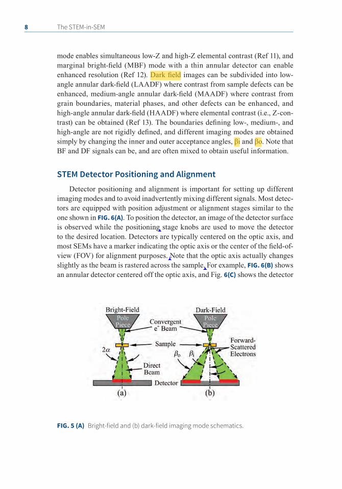
electron scattering distribution, enables implementation of different imaging modes. Broadly speaking, imaging modes can be divided into two catego-ries: bright-field (BF) and dark-field (DF). Bright field images are formed by selecting transmitted electrons that fall within limits defined by the beam con-vergence angle, α (FIG. 5A). The transmitted electrons contained within α are collectively referred to as the direct beam. Dark field images are formed by selecting anything outside the direct beam (FIG. 5B).
Bright field and DF imaging modes can be subdivided into additional modes to obtain specific information. For example, annular bright field (ABF)
8 The STEM-in-SEM
FIG. 5 (A) Bright-field and (b) dark-field imaging mode schematics.
mode enables simultaneous low-Z and high-Z elemental contrast (Ref 11), and marginal bright-field (MBF) mode with a thin annular detector can enable enhanced resolution (Ref 12). Dark field images can be subdivided into low-angle annular dark-field (LAADF) where contrast from sample defects can be enhanced, medium-angle annular dark-field (MAADF) where contrast from grain boundaries, material phases, and other defects can be enhanced, and high-angle annular dark-field (HAADF) where elemental contrast (i.e., Z-con-trast) can be obtained (Ref 13). The boundaries defining low-, medium-, and high-angle are not rigidly defined, and different imaging modes are obtained simply by changing the inner and outer acceptance angles, βi and βo. Note that BF and DF signals can be, and are often mixed to obtain useful information.
STEM Detector Positioning and AlignmentDetector positioning and alignment is important for setting up different
imaging modes and to avoid inadvertently mixing different signals. Most detec-tors are equipped with position adjustment or alignment stages similar to the one shown in FIG. 6(A). To position the detector, an image of the detector surface is observed while the positioning stage knobs are used to move the detector to the desired location. Detectors are typically centered on the optic axis, and most SEMs have a marker indicating the optic axis or the center of the field-of-view (FOV) for alignment purposes. Note that the optic axis actually changes slightly as the beam is rastered across the sample. For example, FIG. 6(B) shows an annular detector centered off the optic axis, and Fig. 6(C) shows the detector

Chapter One Imaging and Diffraction with Commercially Available Transmission Detectors* 9
FIG. 6 Detector positioning. (a) An xyz-positioning stage for a STEM detector. (b) Image of a solid-state detector positioned slightly off the center of the FOV. (c) Detec-tor centered on the FOV.
centered on the optic axis. Be aware that on some SEMs, and especially at high magnifications, beam shift controls may be used automatically to make small changes in, or reposition a feature of interest in the FOV. Beam shift essentially moves the optic axis, and because the STEM detector does not automatically move with the beam shift, this may lead to unintentional signal mixing that can complicate image interpretation. To avoid this, beam shift should be zeroed-out and disabled for STEM imaging.
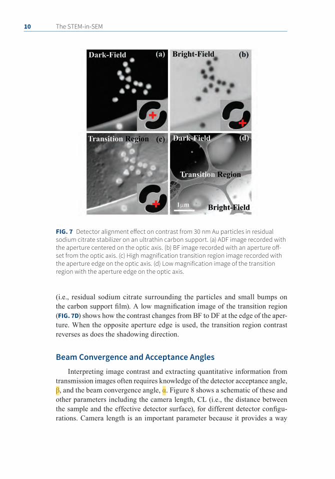
Intentionally moving the detector (or aperture) off the optic axis, however, can sometimes elicit useful contrast (Ref 14, 15). For example, transmission images exhibiting topographic-like contrast (i.e., shadowing) can be obtained by aligning the optic axis with the edge of an aperture or detector. Figure 7 shows the effect using 30 nm gold particles drop-cast on an ultrathin carbon/lacey carbon support film. The DF image (FIG. 7A) was recorded with the aper-ture centered on the optic axis (red cross-hairs), and the BF image (FIG. 7B) was recorded with one of the open annular regions centered on the optic axis. Discrete particles and an edge of the lacey carbon support are visible in both images. The edge of the aperture was then aligned with the optic axis (FIG. 7C, inset) and an image was recorded with focus at the sample (FIG. 7C). Topo-graphic-like contrast can be observed that is not evident in the BF or DF images
10 The STEM-in-SEM
FIG. 7 Detector alignment effect on contrast from 30 nm Au particles in residual sodium citrate stabilizer on an ultrathin carbon support. (a) ADF image recorded with the aperture centered on the optic axis. (b) BF image recorded with an aperture off-set from the optic axis. (c) High magnification transition region image recorded with the aperture edge on the optic axis. (d) Low magnification image of the transition region with the aperture edge on the optic axis.
(i.e., residual sodium citrate surrounding the particles and small bumps on the carbon support film). A low magnification image of the transition region (FIG. 7D) shows how the contrast changes from BF to DF at the edge of the aper-ture. When the opposite aperture edge is used, the transition region contrast reverses as does the shadowing direction.
Beam Convergence and Acceptance AnglesInterpreting image contrast and extracting quantitative information from
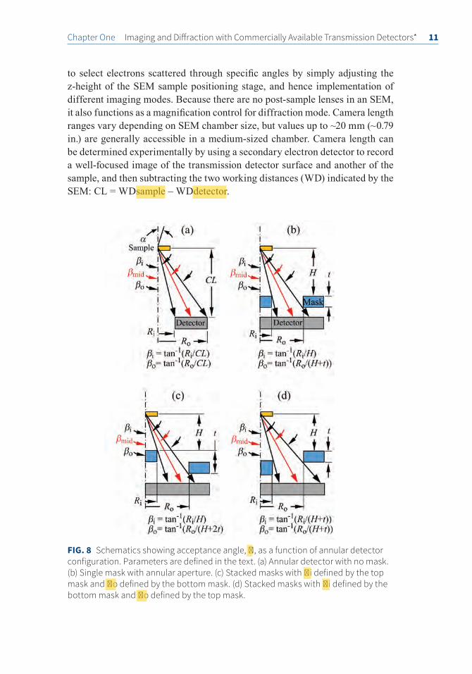
transmission images often requires knowledge of the detector acceptance angle, β, and the beam convergence angle, α. Figure 8 shows a schematic of these and other parameters including the camera length, CL (i.e., the distance between the sample and the effective detector surface), for different detector configu-rations. Camera length is an important parameter because it provides a way
Chapter One Imaging and Diffraction with Commercially Available Transmission Detectors* 11
to select electrons scattered through specific angles by simply adjusting the z-height of the SEM sample positioning stage, and hence implementation of different imaging modes. Because there are no post-sample lenses in an SEM, it also functions as a magnification control for diffraction mode. Camera length ranges vary depending on SEM chamber size, but values up to ~20 mm (~0.79 in.) are generally accessible in a medium-sized chamber. Camera length can be determined experimentally by using a secondary electron detector to record a well-focused image of the transmission detector surface and another of the sample, and then subtracting the two working distances (WD) indicated by the SEM: CL = WDsample – WDdetector.
FIG. 8 Schematics showing acceptance angle, β, as a function of annular detector configuration. Parameters are defined in the text. (a) Annular detector with no mask. (b) Single mask with annular aperture. (c) Stacked masks with βi defined by the top mask and βo defined by the bottom mask. (d) Stacked masks with βi defined by the bottom mask and βo defined by the top mask.
12 The STEM-in-SEM
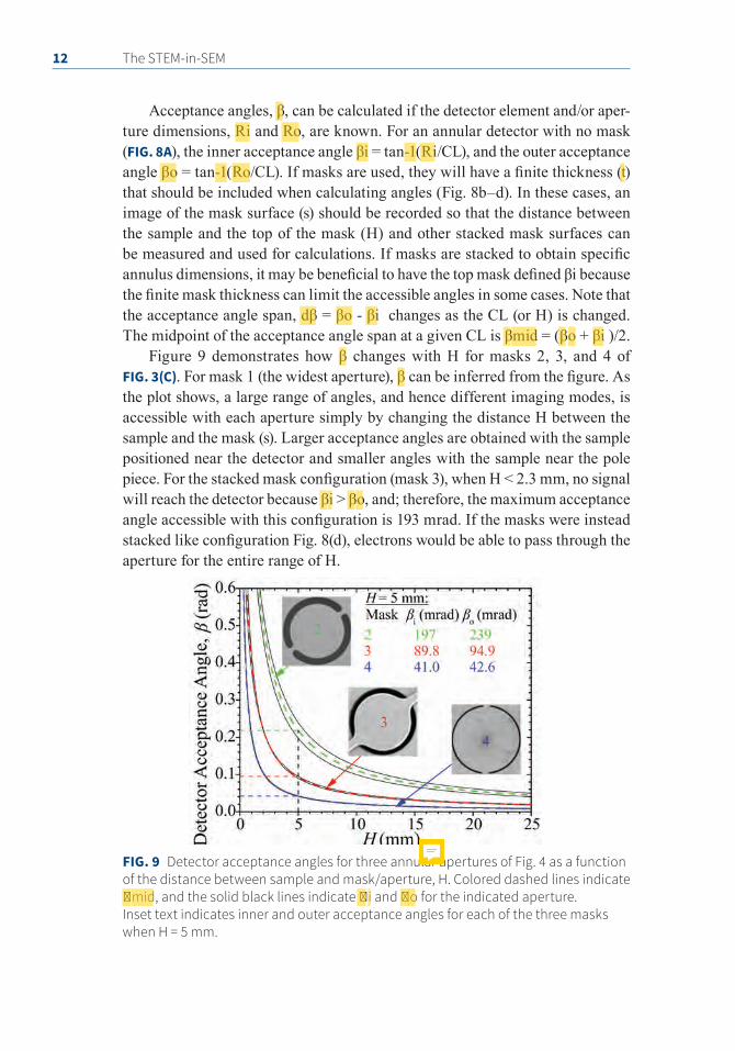
Acceptance angles, β, can be calculated if the detector element and/or aper-ture dimensions, Ri and Ro, are known. For an annular detector with no mask (FIG. 8A), the inner acceptance angle βi = tan-1(Ri/CL), and the outer acceptance angle βo = tan-1(Ro/CL). If masks are used, they will have a finite thickness (t) that should be included when calculating angles (Fig. 8b–d). In these cases, an image of the mask surface (s) should be recorded so that the distance between the sample and the top of the mask (H) and other stacked mask surfaces can be measured and used for calculations. If masks are stacked to obtain specific annulus dimensions, it may be beneficial to have the top mask defined βi because the finite mask thickness can limit the accessible angles in some cases. Note that the acceptance angle span, dβ = βo - βi changes as the CL (or H) is changed. The midpoint of the acceptance angle span at a given CL is βmid = (βo + βi )/2.
Figure 9 demonstrates how β changes with H for masks 2, 3, and 4 of FIG. 3(C). For mask 1 (the widest aperture), β can be inferred from the figure. As the plot shows, a large range of angles, and hence different imaging modes, is accessible with each aperture simply by changing the distance H between the sample and the mask (s). Larger acceptance angles are obtained with the sample positioned near the detector and smaller angles with the sample near the pole piece. For the stacked mask configuration (mask 3), when H < 2.3 mm, no signal will reach the detector because βi > βo, and; therefore, the maximum acceptance angle accessible with this configuration is 193 mrad. If the masks were instead stacked like configuration Fig. 8(d), electrons would be able to pass through the aperture for the entire range of H.
FIG. 9 Detector acceptance angles for three annular apertures of Fig. 4 as a function of the distance between sample and mask/aperture, H. Colored dashed lines indicate βmid, and the solid black lines indicate βi and βo for the indicated aperture. Inset text indicates inner and outer acceptance angles for each of the three masks when H = 5 mm.
Chapter One Imaging and Diffraction with Commercially Available Transmission Detectors* 13
The primary electron beam convergence angle, α,can be controlled to a limited extent on many machines by choosing one of the beam-limiting aper-tures and adjusting the SEM working distance. Some SEMs also have adjustable condenser lenses that can be used to control α albeit usually at the cost of spot size control. As will be shown, different imaging modes and information can be obtained by changing α but it is not necessarily an easy parameter to quantify experimentally. One procedure is to measure the beam diameter at different working distances and apply some basic trigonometry to calculate α (Ref 16). Alternatively, if an on-axis diffraction camera is available, α can be measured by forming a convergent beam electron diffraction (CBED) pattern, measuring the resulting discs, and applying some basic trigonometry (Ref 17). Manufac-turers of SEM may also provide an equation that enables α to be calculated as a function of WD and aperture diameter. To give readers a feel for convergence angles accessible with a common 30 µm beam limiting aperture in one modern SEM, α ≈ 7.5 mrad at WD = 1 mm, and α ≈ 2.5 mrad at WD = 20 mm (Ref 7). Note that illumination becomes more parallel with longer working distances. Also note that larger beam limiting apertures will enable larger convergence angles while smaller apertures will enable smaller convergence angles (i.e., more parallel illumination). Parallel and convergent illumination are important concepts, especially for imaging in diffraction mode.
Using the MasksBeyond enabling different imaging modes, masks can be used to quantify
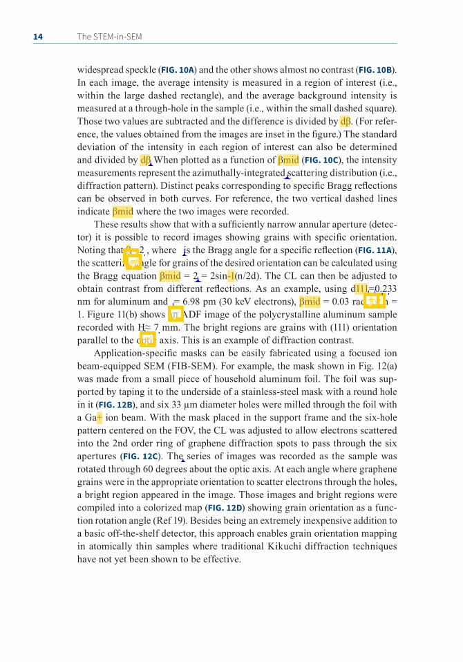
transmitted electron scattering distributions (i.e., diffraction patterns), which in turn can help with image contrast interpretation. Figure 10 demonstrates the process for a polycrystalline aluminum sample. First, a sufficiently nar-row aperture is selected (Ref 18) and the relationship between CL and β is calculated. Note that dβ must be sufficiently small that only a narrow slice of the scattering distribution can hit the detector, otherwise the signal may be integrated over too large a range to discern fine details in the scattering dis-tribution. Then, with the annulus centered on the optic axis, the SEM sample positioning stage is used to step the sample through the available CL in small increments of Δz. At each step, and with the STEM detector gain settings held constant, a focused image of the sample is recorded. The detector gain setting should be adjusted such that the minimum gray level is always greater than zero, and the maximum gray level does not saturate the detector in any of the images. This requires some initial investigation to determine βmid at which the image exhibits the greatest intensity.
Figure 10 shows two cropped images of the polycrystalline aluminum sample recorded at different CLs using mask 4 of Fig. 3. One image shows
14 The STEM-in-SEM
widespread speckle (FIG. 10A) and the other shows almost no contrast (FIG. 10B). In each image, the average intensity is measured in a region of interest (i.e., within the large dashed rectangle), and the average background intensity is measured at a through-hole in the sample (i.e., within the small dashed square). Those two values are subtracted and the difference is divided by dβ. (For refer-ence, the values obtained from the images are inset in the figure.) The standard deviation of the intensity in each region of interest can also be determined and divided by dβ When plotted as a function of βmid (FIG. 10C), the intensity measurements represent the azimuthally-integrated scattering distribution (i.e., diffraction pattern). Distinct peaks corresponding to specific Bragg reflections can be observed in both curves. For reference, the two vertical dashed lines indicate βmid where the two images were recorded.
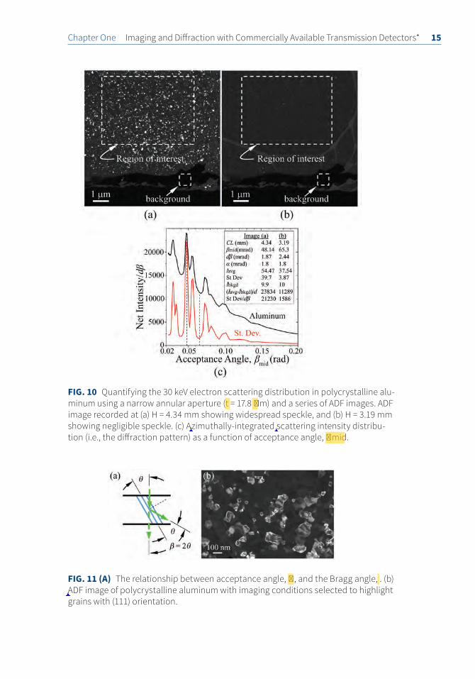
These results show that with a sufficiently narrow annular aperture (detec-tor) it is possible to record images showing grains with specific orientation. Noting that β= 2 , where is the Bragg angle for a specific reflection (FIG. 11A), the scattering angle for grains of the desired orientation can be calculated using the Bragg equation βmid = 2 = 2sin-1(n/2d). The CL can then be adjusted to obtain contrast from different reflections. As an example, using d111=0.233 nm for aluminum and = 6.98 pm (30 keV electrons), βmid = 0.03 rad for n = 1. Figure 11(b) shows an ADF image of the polycrystalline aluminum sample recorded with H≈ 7 mm. The bright regions are grains with (111) orientation parallel to the optic axis. This is an example of diffraction contrast.
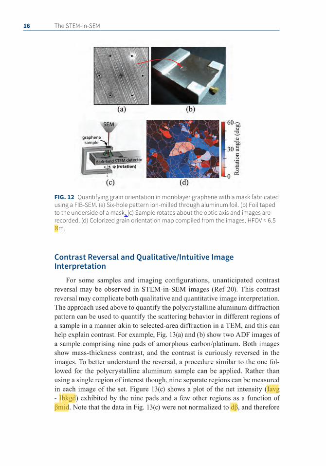
Application-specific masks can be easily fabricated using a focused ion beam-equipped SEM (FIB-SEM). For example, the mask shown in Fig. 12(a) was made from a small piece of household aluminum foil. The foil was sup-ported by taping it to the underside of a stainless-steel mask with a round hole in it (FIG. 12B), and six 33 µm diameter holes were milled through the foil with a Ga+ ion beam. With the mask placed in the support frame and the six-hole pattern centered on the FOV, the CL was adjusted to allow electrons scattered into the 2nd order ring of graphene diffraction spots to pass through the six apertures (FIG. 12C). The series of images was recorded as the sample was rotated through 60 degrees about the optic axis. At each angle where graphene grains were in the appropriate orientation to scatter electrons through the holes, a bright region appeared in the image. Those images and bright regions were compiled into a colorized map (FIG. 12D) showing grain orientation as a func-tion rotation angle (Ref 19). Besides being an extremely inexpensive addition to a basic off-the-shelf detector, this approach enables grain orientation mapping in atomically thin samples where traditional Kikuchi diffraction techniques have not yet been shown to be effective.
Chapter One Imaging and Diffraction with Commercially Available Transmission Detectors* 15
FIG. 10 Quantifying the 30 keV electron scattering distribution in polycrystalline alu-minum using a narrow annular aperture (t = 17.8 βm) and a series of ADF images. ADF image recorded at (a) H = 4.34 mm showing widespread speckle, and (b) H = 3.19 mm showing negligible speckle. (c) Azimuthally-integrated scattering intensity distribu-tion (i.e., the diffraction pattern) as a function of acceptance angle, βmid.
FIG. 11 (A) The relationship between acceptance angle, β, and the Bragg angle, . (b) ADF image of polycrystalline aluminum with imaging conditions selected to highlight grains with (111) orientation.
16 The STEM-in-SEM
Contrast Reversal and Qualitative/Intuitive Image Interpretation
For some samples and imaging configurations, unanticipated contrast reversal may be observed in STEM-in-SEM images (Ref 20). This contrast reversal may complicate both qualitative and quantitative image interpretation. The approach used above to quantify the polycrystalline aluminum diffraction pattern can be used to quantify the scattering behavior in different regions of a sample in a manner akin to selected-area diffraction in a TEM, and this can help explain contrast. For example, Fig. 13(a) and (b) show two ADF images of a sample comprising nine pads of amorphous carbon/platinum. Both images show mass-thickness contrast, and the contrast is curiously reversed in the images. To better understand the reversal, a procedure similar to the one fol-lowed for the polycrystalline aluminum sample can be applied. Rather than using a single region of interest though, nine separate regions can be measured in each image of the set. Figure 13(c) shows a plot of the net intensity (Iavg - Ibkgd) exhibited by the nine pads and a few other regions as a function of βmid. Note that the data in Fig. 13(c) were not normalized to dβ, and therefore
FIG. 12 Quantifying grain orientation in monolayer graphene with a mask fabricated using a FIB-SEM. (a) Six-hole pattern ion-milled through aluminum foil. (b) Foil taped to the underside of a mask. (c) Sample rotates about the optic axis and images are recorded. (d) Colorized grain orientation map compiled from the images. HFOV ≈ 6.5 βm.

Chapter One Imaging and Diffraction with Commercially Available Transmission Detectors* 17
graphically represent what is observed by eye in the images at different CLs. When the data set is normalized to dβ (FIG. 13D); however, it more accurately represents the electron scattering distribution.
Both Fig. 13(c) and (d) show that image intensities are not a monotonic function of thickness and do not necessarily reflect the sample thickness in an intuitive manner when 30 < β < 200 mrad. If qualitative thickness informa-tion is desired, imaging conditions should be set to select electrons scattered outside this range. A reasonable conclusion might be to record a BF image and use that for mass-thickness contrast interpretation. The challenge with that approach is that most BF detectors are sufficiently large to collect all of the BF signal and a notable portion of the DF signal. This complicates contrast interpretation because images collected over a large acceptance angle may exhibit intensities that are averaged in a complex way and may not necessarily be representative of sample thickness. Intensity distributions of the thinnest regions also exhibit local maxima suggesting short-range structural ordering (Ref 21). With increasing sample thickness, those local maxima disappear, and the distributions broaden because of the increasing number of scattering events
FIG. 13 Contrast reversal and intensity distributions in images of an amorphous car-bon/platinum sample with nine pads of different thickness. ADF image (a) low-angle, (b) high-angle. (c) Intensity distributions for each of the nine pads. (d) Intensity dis-tributions normalized to dβ. Vertical dashed lines indicate βmid at which the images were recorded.

18 The STEM-in-SEM
resulting in random forward-scattering of the probe electrons. This suggests a limit to sample thickness for obtaining short- and medium-range structural information about the sample.
To that end, sample thickness is one of the biggest challenges for STEM-in-SEM imaging. In general, thinner is better but it depends on the application. For example, samples for grain orientation mapping by transmission Kikuchi diffraction (Ref 3) must be thick enough to allow inelastic scattering and the successive elastic scattering processes that elicit Kikuchi lines. Putting sample thickness into perspective, the total mean free path (mfp, elastic + inelastic) for 10 keV electrons in carbon is approximately 4.4 nm, and for 30 keV electrons it is closer to 14 nm. For gold, the total mfp is approximately 1.3 nm at 10 keV and 2.7 nm at 30 keV (Ref 22). In an ideal world, samples would be no more than one mfp thick so that contrast is more amenable to direct interpretation by eye and substantiation by simulation. Realistically, though, samples can still be several mfp thick and still be amenable to analytical interpretation.
Chapter One Imaging and Diffraction with Commercially Available Transmission Detectors* 19
References
1. E. Buhr, et al., Characterization of Nanoparticles by Scanning Electron Micros-copy in Transmission Mode, Meas. Sci. Technol., Vol 20 (No. 8), 2009, 20, p 084025–084025-9. https://doi.org/10.1088/0957-0233/20/8/084025
2. M. Kuwajima, et al.,Automated Transmission-Mode Scanning Electron Micros-copy (tSEM) for Large Volume Analysis at Nanoscale Resolution, PLOS ONE, Vol 8 (No. 3), 2013, 8, p e59573–e59573-9. https://doi.org/10.1371/journal.pone.0059573
3. R.H. Geiss, et al., Transmission EBSD in the Scanning Electron Microscope, Microscopy Today, Vol 21 (No. 1), 2013, p 16–20. https://doi.org/10.1017/S1551929513000503
4. P.W. Trimby, “Orientation Mapping of Nanostructured Materials Using Transmission Kikuchi Diffraction in the Scanning Electron Micro-scope,” Ultramicroscopy, Vol 120, 2012, p 16–24. https://doi.org/10.1016/j.ultramic.2012.06.004
5. C. Sun, et al., Analysis of Crystal Defects by Scanning Transmission Elec-tron Microscopy (STEM) in a Modern Scanning Electron Microscope, Adv. Struct. Chem. Imag., Vol 5 (No. 1), 2019, p 1–9. https://doi.org/10.1186/s40679-019-0065-1
6. P.G. Callahans, et al., Transmission Scanning Electron Microscopy: Defect Observations and Image Simulations, Ultramicroscopy, Vol 186, 2018, p 49–61. https://doi.org/10.1016/j.ultramic.2017.11.004
7. B. Caplins, et al., Transmission Imaging with a Programmable Detector in a Scanning Electron Microscope, Ultramicroscopy, Vol 196, 2019, p 40–48. https://doi.org/10.1016/j.ultramic.2018.09.006
8. R.F. Egerton, et al., Radiation Damage in the TEM and SEM, Micron., Vol 35 (No. 6), 2004, p 399–409. https://doi.org/10.1016/j.micron.2004.02.003
9. B.J. Crawford and C.R.W. Liley, A Simple Transmission Stage Using the Standard Collection System in the Scanning Electron Microscope, J. Phys. E: Sci. Instrum., Vol 3 (No. 6), 1970, 3, p 461–462. https://doi.org/10.1088/0022-3735/3/6/314
10. J. Holm and RR. Keller, Acceptance Angle Control for Improved Transmis-sion Imaging in an SEM, Microscopy Today, Vol 2 (No. 1), 2017, p 12–19. https://doi.org/10.1017/S1551929516001267
11. S.D. Findlay, et al., Dynamics of Annular Bright Field Imaging in Scanning Transmission Electron Microscopy, Ultramicroscopy, Vol 110, 2010, p 903–923. https://doi.org/10.1016/j.ultramic.2010.04.004
12. R.J. Liu and J.M. Cowley, Dark-Field and Marginal Imaging with a Thin-Annu-lar Detector in STEM, Microsc. Microanal., Vol 2 (No. 1), 1996, p 9–19. https://doi.org/10.1017/S1431927696210098
20 The STEM-in-SEM
13. S.J. Pennycook and P.D. Nellist, Scanning Transmission Electron Microscopy, Springer-Verlag, 2011
14. G.B. Haydon and R.A. Lemons, Optical Shadowing in the Electron Microscope, J. Microsc., Vol 95 (No. 3), 1972, p 483–891. https://doi.org/10.1111/j.1365-2818.1972.tb01052.x
15. A.G. Cullis and D.M. Maher, Topographical Contrast in the Transmission Electron Microscope, Ultramicroscopy, Vol 1, 1975, p 97–112. https://doi.org/10.1016/S0304-3991(75)80012-X
16. C. Lyman, et al., Scanning Electron Microscopy, X-Ray Microanalysis, and Ana-lytical Electron Microscopy, Plenum Press, 1990, p 12
17. D.B. Williams and C.B. Carter, Electron Sources, Transmission Electron Microscopy, Plenum Publishing, 1996
18. J. Holm, Scattering Intensity Distribution Dependence on Collection Angles in Annular Dark-Field STEM-in-SEM Images, Ultramicroscopy, Vol 195, 2018, p 12–20. https://doi.org/10.1016/j.ultramic.2018.06.007
19. B. Caplins, et al., Orientation Mapping of Graphene in a Scanning Electron Microscope, Carbon, Vol 149, 2019, p 400–406. https://doi.org/10.1016/j.carbon.2019.04.042
20. P.G. Merli, et al., Backscattered Electron Imaging and Scanning Transmis-sion Electron Microscopy Imaging of Multi-Layers, Ultramicroscopy, Vol 94, 2003, p 89–98. https://doi.org/10.1016/S0304-3991(02)00217-6
21. D.J.H. Cockayne, The Study of Nanovolumes of Amorphous Materials Using Electron Scattering, Annu. Rev. Mater. Res., Vol 37 (No. 1), 2007, p 159–187. https://doi.org/10.1146/annurev.matsci.35.082803.103337
22. L. Reimer, Scanning Electron Microscopy, Vol 45, Springer Series in Optical Sciences,, Springer-Verlag, 1985
STEM-in-SEMJ.D. Holm and B.W. Caplins
Copyright © 2020 ASM International® All rights reserved
www.asminternational.org
21
C h a p t e r T w o
Imaging and Diffraction with a Programmable Pixelated Detector
INTRODUCTIONIn this chapter, a digital detector that enables both imaging and diffraction
in one programmable system is described (Ref 1). The commentary provided here is not exclusive to this detector, and much of it can be applied to emerging digital systems for STEM-in-SEM imaging and diffraction applications (Ref 2).
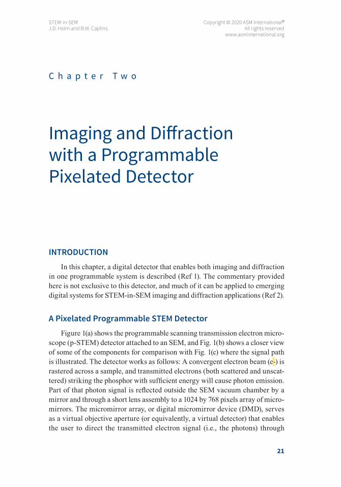
A Pixelated Programmable STEM DetectorFigure 1(a) shows the programmable scanning transmission electron micro-
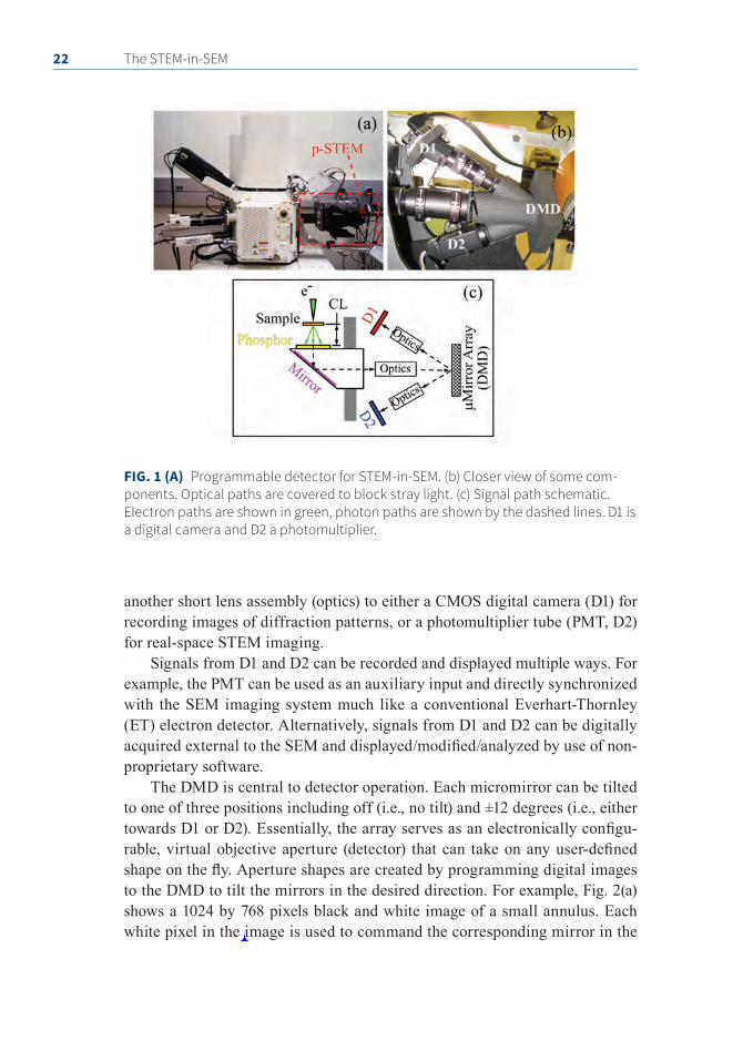
scope (p-STEM) detector attached to an SEM, and Fig. 1(b) shows a closer view of some of the components for comparison with Fig. 1(c) where the signal path is illustrated. The detector works as follows: A convergent electron beam (e-) is rastered across a sample, and transmitted electrons (both scattered and unscat-tered) striking the phosphor with sufficient energy will cause photon emission. Part of that photon signal is reflected outside the SEM vacuum chamber by a mirror and through a short lens assembly to a 1024 by 768 pixels array of micro-mirrors. The micromirror array, or digital micromirror device (DMD), serves as a virtual objective aperture (or equivalently, a virtual detector) that enables the user to direct the transmitted electron signal (i.e., the photons) through
22 The STEM-in-SEM
another short lens assembly (optics) to either a CMOS digital camera (D1) for recording images of diffraction patterns, or a photomultiplier tube (PMT, D2) for real-space STEM imaging.
Signals from D1 and D2 can be recorded and displayed multiple ways. For example, the PMT can be used as an auxiliary input and directly synchronized with the SEM imaging system much like a conventional Everhart-Thornley (ET) electron detector. Alternatively, signals from D1 and D2 can be digitally acquired external to the SEM and displayed/modified/analyzed by use of non-proprietary software.
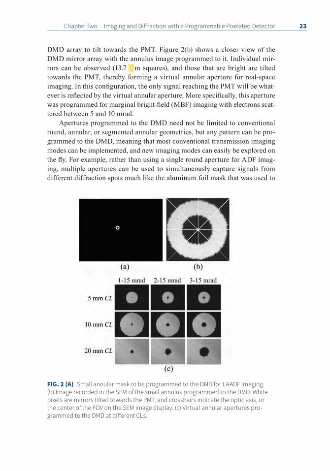
The DMD is central to detector operation. Each micromirror can be tilted to one of three positions including off (i.e., no tilt) and ±12 degrees (i.e., either towards D1 or D2). Essentially, the array serves as an electronically configu-rable, virtual objective aperture (detector) that can take on any user-defined shape on the fly. Aperture shapes are created by programming digital images to the DMD to tilt the mirrors in the desired direction. For example, Fig. 2(a) shows a 1024 by 768 pixels black and white image of a small annulus. Each white pixel in the image is used to command the corresponding mirror in the
FIG. 1 (A) Programmable detector for STEM-in-SEM. (b) Closer view of some com-ponents. Optical paths are covered to block stray light. (c) Signal path schematic. Electron paths are shown in green, photon paths are shown by the dashed lines. D1 is a digital camera and D2 a photomultiplier.
Chapter Two Imaging and Diffraction with a Programmable Pixelated Detector 23
DMD array to tilt towards the PMT. Figure 2(b) shows a closer view of the DMD mirror array with the annulus image programmed to it. Individual mir-rors can be observed (13.7 m squares), and those that are bright are tilted towards the PMT, thereby forming a virtual annular aperture for real-space imaging. In this configuration, the only signal reaching the PMT will be what-ever is reflected by the virtual annular aperture. More specifically, this aperture was programmed for marginal bright-field (MBF) imaging with electrons scat-tered between 5 and 10 mrad.
Apertures programmed to the DMD need not be limited to conventional round, annular, or segmented annular geometries, but any pattern can be pro-grammed to the DMD, meaning that most conventional transmission imaging modes can be implemented, and new imaging modes can easily be explored on the fly. For example, rather than using a single round aperture for ADF imag-ing, multiple apertures can be used to simultaneously capture signals from different diffraction spots much like the aluminum foil mask that was used to
FIG. 2 (A) Small annular mask to be programmed to the DMD for LAADF imaging. (b) Image recorded in the SEM of the small annulus programmed to the DMD. White pixels are mirrors tilted towards the PMT, and crosshairs indicate the optic axis, or the center of the FOV on the SEM image display. (c) Virtual annular apertures pro-grammed to the DMD at different CLs.
24 The STEM-in-SEM
quantify graphene grain orientation in chapter 1. Moreover, the ability to auto-mate imaging with programmable scripts to tilt different mirrors incrementally or in specific patterns is feasible either with the DMD software or with other commercial or open-source software. Additionally, all of the DMD mirrors can be tilted towards the camera so that a diffraction pattern can be captured at each raster spot. In this way, many of the emerging 4D STEM techniques (Ref 3) are possible in an SEM.
Detector alignment is also important with this system, and several align-ments may be necessary depending on the goal of the imaging session. An xyz-positioning stage is used for coarse mechanical alignment. The idea is to approximately center the DMD array on the optic axis, and to optimize the space between the phosphor and the pole piece (i.e., to maximize the available CL). Another alignment involves positioning the aperture(s). For example, the annular pattern in Fig. 2(b) is nearly centered on the optic axis, but the annulus is not centered in the digital image programmed to the DMD (Fig. 2a), nor does it need to be. Although the virtual apertures can be positioned mechanically using the xyz-positioning stage, it is easier to position them electronically by tilting different mirrors. A more critical alignment, perhaps, is between the object plane and the detector image plane. (Note that the phosphor is effectively the object plane.) This step is required to ensure that STEM images and diffrac-tion patterns are not rotated, distorted, or otherwise out of alignment with each other, and that objects in images recorded with other SEM detectors align with objects recorded in STEM images. These image/object plane misalignments are determined electronically, and if desired, corrections can be automatically applied to images and diffraction patterns (Ref 1).
As with any digital imaging system, the pixelated signal must be considered. This is especially important for the small angles associated with electron scat-tering. For example, Fig. 2(c) shows different annular apertures programmed to the DMD at different CLs. When short CLs are used to collect signals at very small acceptance angles, individual pixels (i.e., mirrors) may not be small enough to accurately reproduce an aperture (detector) with the intended shape. For example, at 5 mm CL, a single mirror defines βi = 1 mrad, but eight mirrors define βi = 2 mrad, meaning that the aperture is better approximated as round with more mirrors. Moreover, useful intensity variation may exist within a small scattering angle (i.e., there is almost always intensity variation within the direct beam, and often in convergent beam electron diffraction (CBED) discs) that a single mirror will not be able to resolve. Longer CLs will generally enable better resolution by allowing more mirrors to reflect the signal.
Chapter Two Imaging and Diffraction with a Programmable Pixelated Detector 25
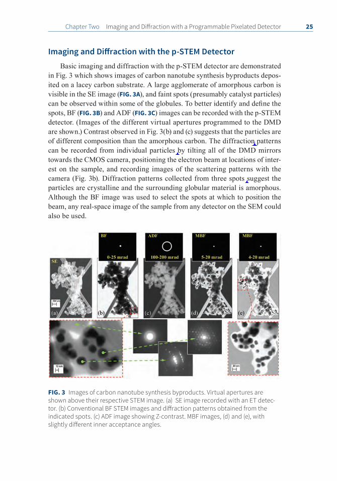
Imaging and Diffraction with the p-STEM DetectorBasic imaging and diffraction with the p-STEM detector are demonstrated
in Fig. 3 which shows images of carbon nanotube synthesis byproducts depos-ited on a lacey carbon substrate. A large agglomerate of amorphous carbon is visible in the SE image (FIG. 3A), and faint spots (presumably catalyst particles) can be observed within some of the globules. To better identify and define the spots, BF (FIG. 3B) and ADF (FIG. 3C) images can be recorded with the p-STEM detector. (Images of the different virtual apertures programmed to the DMD are shown.) Contrast observed in Fig. 3(b) and (c) suggests that the particles are of different composition than the amorphous carbon. The diffraction patterns can be recorded from individual particles by tilting all of the DMD mirrors towards the CMOS camera, positioning the electron beam at locations of inter-est on the sample, and recording images of the scattering patterns with the camera (Fig. 3b). Diffraction patterns collected from three spots suggest the particles are crystalline and the surrounding globular material is amorphous. Although the BF image was used to select the spots at which to position the beam, any real-space image of the sample from any detector on the SEM could also be used.
FIG. 3 Images of carbon nanotube synthesis byproducts. Virtual apertures are shown above their respective STEM image. (a) SE image recorded with an ET detec-tor. (b) Conventional BF STEM images and diffraction patterns obtained from the indicated spots. (c) ADF image showing Z-contrast. MBF images, (d) and (e), with slightly different inner acceptance angles.

26 The STEM-in-SEM
Figures 3(d) and (e) show additional detector utility. Here, two nearly identi-cal apertures were programmed to the DMD to demonstrate MBF imaging. In this mode, both low-Z and high-Z components are simultaneously visible, and the catalyst particles can be easily discerned from the amorphous carbon. A closer view (Fig. 3e) reveals contrast variation suggestive of structural inhomo-geneity within many particles. Perhaps the most apparent difference between the two images, however, is the background. When βi = 5 mrad (Fig. 3d), the background is dark because the signal from the direct beam is blocked by the aperture. When βi = 4 mrad (FIG. 3E), the background is brighter because the aperture allows part of the direct beam to contribute to the image signal. By varying the aperture inner radius, α can be quantified and an equation developed to estimate its value at different working distances and for different beam-limiting apertures (Ref 1). For the SEM used here, ≈ 2.73 D / (12.4 + WD), where D (mm) is the beam limiting aperture diameter and WD (mm) is the working distance indicated by the SEM. So, in addition to enabling noncon-ventional imaging modes, the detector can also be used to glean information about the SEM.
Diffraction patterns are not limited to being obtained from discrete points on the sample, but can also be obtained from large areas. This is useful for beam-sensitive materials like the sample shown in Fig. 4. Here, ~4.6 nm thick zeolite sheets (Ref 4) were imaged in ADF mode with the indicated aperture programmed to the DMD. The rectangular areas of adventitious carbon indicate the regions from which the diffraction patterns were obtained. Total integration time for each diffraction pattern was ~2 seconds with very short pixel dwell time. Although significantly shorter integration times are feasible, this setting was used so that contrast in the diffraction patterns could be observed by eye with no digital image enhancement.
The images and diffraction patterns in Fig. 4(a) also demonstrate the impor-tance of detector alignment. For example, zeolites in the ADF image exhibit a distinct orientation that the diffraction pattern should replicate. The diffrac-tion pattern on the top-right is shown without applying the detector alignment correction, and the pattern does not align well with the zeolite sheet. Detector misalignment was accounted for in the other two diffraction patterns, and both are well-aligned with the sheets as they appear in the real-space ADF image. Notice that the diffraction pattern in the lower-left was recorded from an area of two overlapping and slightly rotated sheets. The slightly rotated sets of diffrac-tion spots can be used to measure the relative rotation between the two sheets. Relative rotation information can also be obtained from moiré fringes, which are large-scale interference patterns that can be produced when an opaque ruled pattern with transparent gaps is overlaid on another similar pattern (FIG 4B).

Chapter Two Imaging and Diffraction with a Programmable Pixelated Detector 27
Here, the superlattice due to two stacked sheets varies because the sheet align-ment varies (Ref 5).
The next example demonstrates another method to visualize and quantify grain orientation in monolayer graphene. Figure 5(a) shows a secondary elec-tron (SE) image of dirty monolayer graphene with a few torn areas. There is no way to discern anything about grain orientation from the SE image, and transmission Kikuchi diffraction techniques commonly used to determine grain orientation in SEMs will not work with this sample. Two points were chosen in this image, and diffraction patterns were obtained at those locations with the p-STEM detector (FIG. 5B AND C). Twelve faint but distinct spots can be observed in each diffraction pattern, and the 12-spot patterns are rotated with respect to each other by ~10.5 degrees. Twelve small circles, each cor-responding to a distinct 4 mrad aperture, were then drawn over the 12 spots in diffraction pattern 1 (FIG. 5D, green circles), and an image file (FIG. 5E) was generated based on those 12 circles. With the image file programmed to the
FIG. 4 ADF STEM images of 2D zeolite sheets (a) obtained using a 30 – 250 mrad vir-tual annular aperture and various diffraction patterns, and (b) showing moiré fringes.
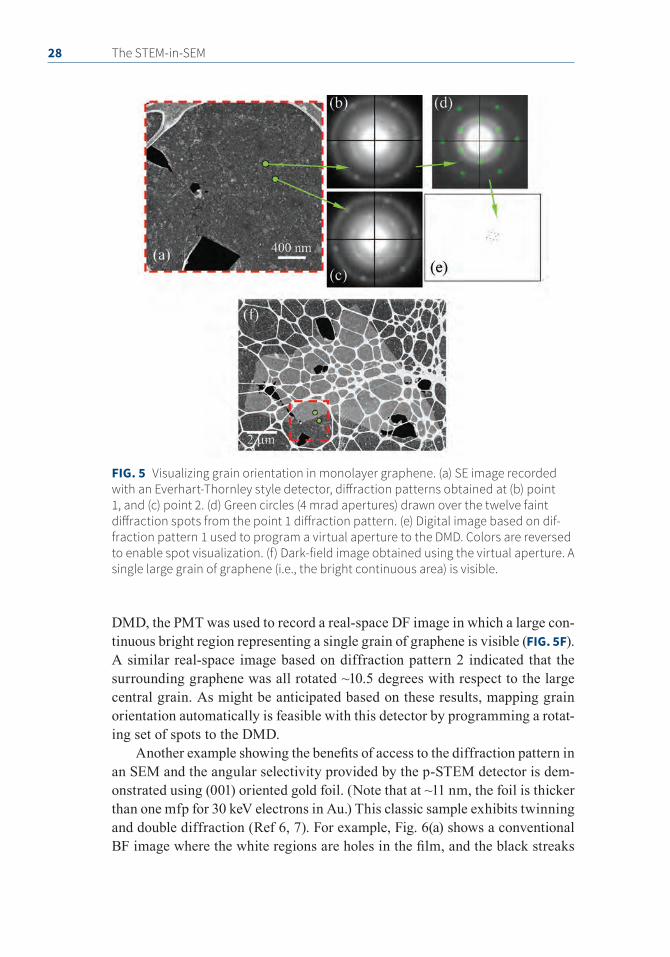
28 The STEM-in-SEM
DMD, the PMT was used to record a real-space DF image in which a large con-tinuous bright region representing a single grain of graphene is visible (FIG. 5F). A similar real-space image based on diffraction pattern 2 indicated that the surrounding graphene was all rotated ~10.5 degrees with respect to the large central grain. As might be anticipated based on these results, mapping grain orientation automatically is feasible with this detector by programming a rotat-ing set of spots to the DMD.
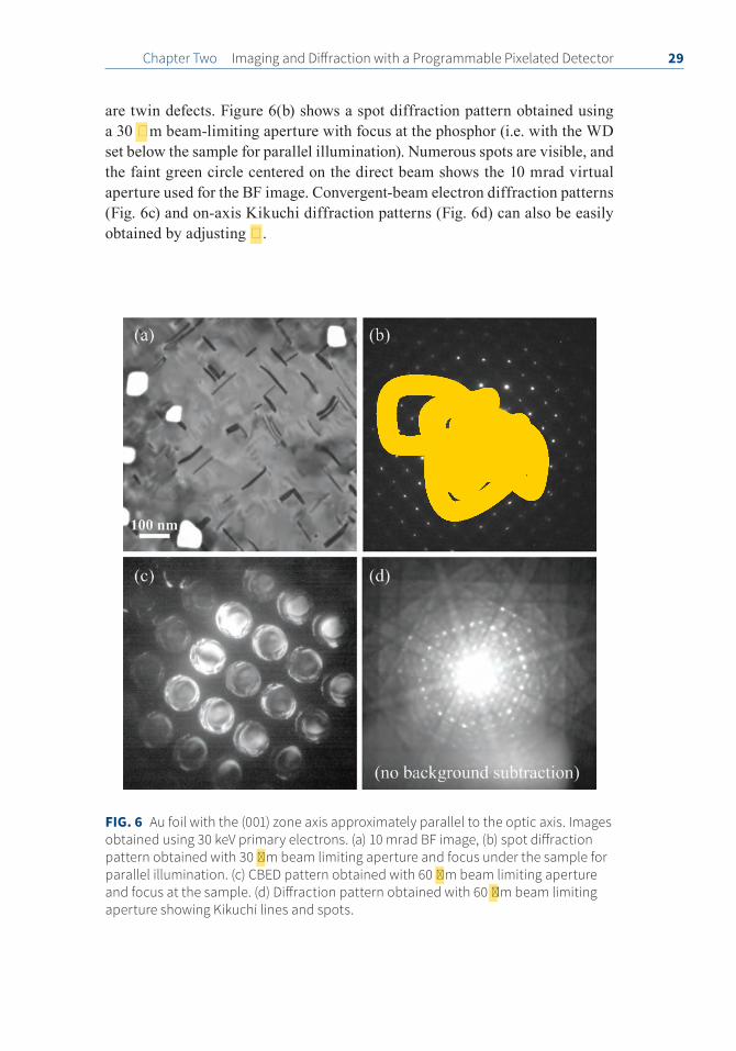
Another example showing the benefits of access to the diffraction pattern in an SEM and the angular selectivity provided by the p-STEM detector is dem-onstrated using (001) oriented gold foil. (Note that at ~11 nm, the foil is thicker than one mfp for 30 keV electrons in Au.) This classic sample exhibits twinning and double diffraction (Ref 6, 7). For example, Fig. 6(a) shows a conventional BF image where the white regions are holes in the film, and the black streaks
FIG. 5 Visualizing grain orientation in monolayer graphene. (a) SE image recorded with an Everhart-Thornley style detector, diffraction patterns obtained at (b) point 1, and (c) point 2. (d) Green circles (4 mrad apertures) drawn over the twelve faint diffraction spots from the point 1 diffraction pattern. (e) Digital image based on dif-fraction pattern 1 used to program a virtual aperture to the DMD. Colors are reversed to enable spot visualization. (f) Dark-field image obtained using the virtual aperture. A single large grain of graphene (i.e., the bright continuous area) is visible.
Chapter Two Imaging and Diffraction with a Programmable Pixelated Detector 29
are twin defects. Figure 6(b) shows a spot diffraction pattern obtained using a 30 m beam-limiting aperture with focus at the phosphor (i.e. with the WD set below the sample for parallel illumination). Numerous spots are visible, and the faint green circle centered on the direct beam shows the 10 mrad virtual aperture used for the BF image. Convergent-beam electron diffraction patterns (Fig. 6c) and on-axis Kikuchi diffraction patterns (Fig. 6d) can also be easily obtained by adjusting .
FIG. 6 Au foil with the (001) zone axis approximately parallel to the optic axis. Images obtained using 30 keV primary electrons. (a) 10 mrad BF image, (b) spot diffraction pattern obtained with 30 βm beam limiting aperture and focus under the sample for parallel illumination. (c) CBED pattern obtained with 60 βm beam limiting aperture and focus at the sample. (d) Diffraction pattern obtained with 60 βm beam limiting aperture showing Kikuchi lines and spots.

30 The STEM-in-SEM
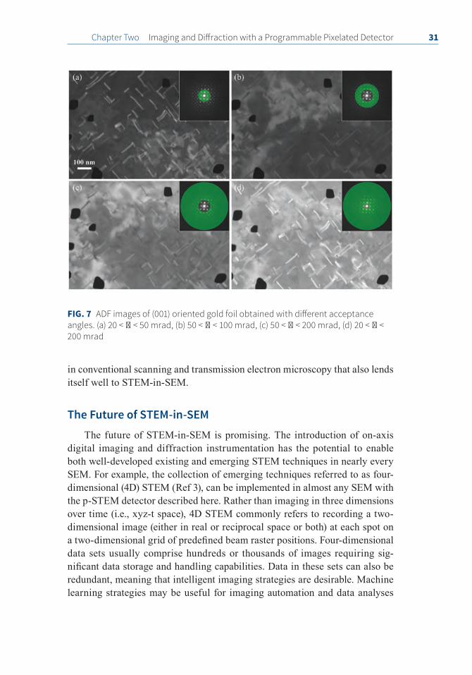
Conventional annular imaging modes and the different contrast that can be observed in these modes from the Au foil are shown in Fig. 7. It shows a LAADF image (20 < β < 50 mrad, indicated by the green annulus in the inset diffraction pattern). The short streaks (i.e., twinned regions) exhibit greater intensity than the rest of the sample, emphasizing the utility of the imaging mode for defect contrast enhancement. Figure 7(b) shows a MAADF image (50 < β < 100 mrad). Defects are faint but still visible, and matrix regions show stronger contrast with respect to the background vacuum intensity. The acceptance angle is widened in Fig. 7(c) (50 < α < 100 mrad), and although the image intensity increases overall, it is not immediately apparent that the image is different from Fig. 7(b). It does, however, show variation in bright regions compared to the BF image in Fig. 6(a). Figure 7d shows an ADF image com-prising a large portion of the scattered electron signal (20 < β < 200 mrad). The contrast is complementary to that observed in the BF image.
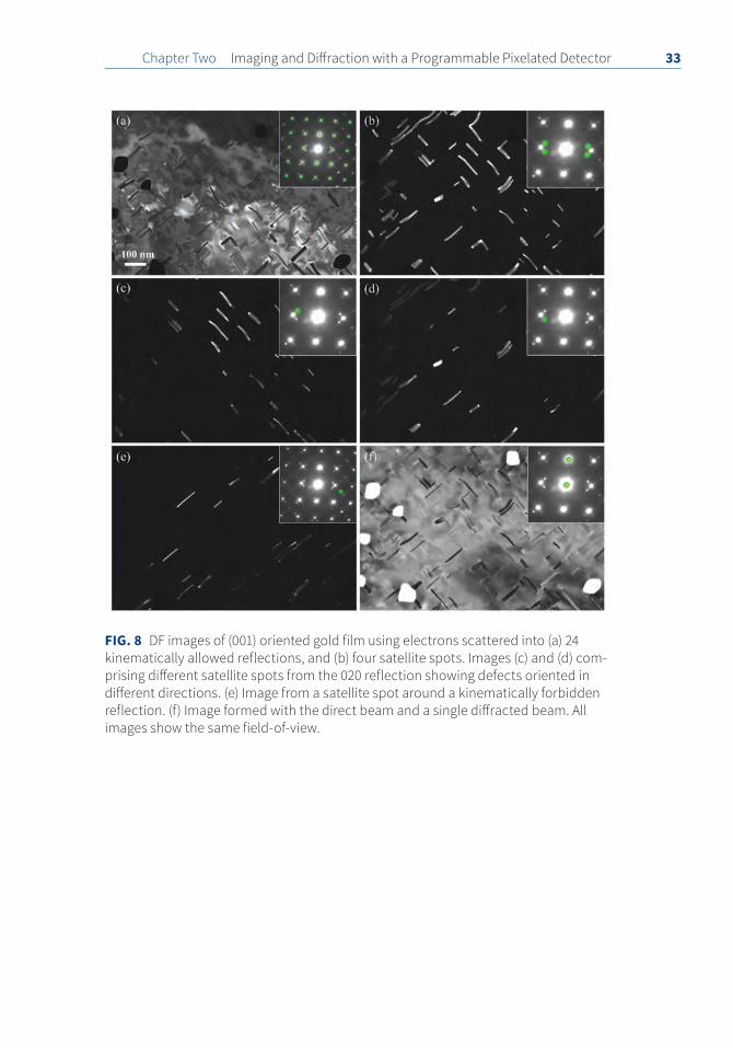
The images in Fig. 7 show the utility of annular imaging modes, specifically that different imaging modes reveal different microstructure aspects includ-ing defects. However, other imaging modes may be better for defect analysis. Therefore, consider the diffraction pattern of Fig. 6(b). Kinematically allowed diffraction spots, several small satellites around those spots, and other miscel-laneous spots (sometimes referred to as forbidden reflections) can be observed among and around the allowed spots. The satellites around the allowed spots are due to double diffraction from the twinned regions (Ref 6). Figure 8 shows how those and other spots can be selected to show defect and other contrast. For example, Figure 8(a) shows a DF image recorded with electrons scattered into 24 allowed spots highlighted by the green circles in the inset diffraction pattern. (Each green circle represents a 4 mrad aperture.) No intensity associ-ated with twin defects is apparent in the real-space images, but the defects can still be observed as dark streaks. To observe intensity due to twin defects, dif-ferent satellite spots can be selected as shown in Fig. 8(b) to (f). For example, multiple spots can be selected to increase defect image intensity (Fig. 8b), or single spots can be selected to visualize twins with specific orientation (Fig. 8 c and d). Figure 8(e) shows an image from electrons scattered into what appears to be a satellite around a forbidden reflection. Figure 8(f) shows an image comprising the direct beam and a (200) reflection in which different parts of the twin defects are highlighted compared to Fig. 7(a) and 8(b). These images were collected on the fly in only a few minutes by observing the diffraction pattern and manually selecting specific electrons to form the different image signals. No specimen tilting is necessary to establish specific diffraction condi-tions. It is also possible to collect a diffraction pattern at each beam raster spot and reconstruct the real-space images based on the set of diffraction patterns. This image reconstruction approach is one of numerous recent developments
Chapter Two Imaging and Diffraction with a Programmable Pixelated Detector 31
in conventional scanning and transmission electron microscopy that also lends itself well to STEM-in-SEM.
The Future of STEM-in-SEMThe future of STEM-in-SEM is promising. The introduction of on-axis
digital imaging and diffraction instrumentation has the potential to enable both well-developed existing and emerging STEM techniques in nearly every SEM. For example, the collection of emerging techniques referred to as four-dimensional (4D) STEM (Ref 3), can be implemented in almost any SEM with the p-STEM detector described here. Rather than imaging in three dimensions over time (i.e., xyz-t space), 4D STEM commonly refers to recording a two-dimensional image (either in real or reciprocal space or both) at each spot on a two-dimensional grid of predefined beam raster positions. Four-dimensional data sets usually comprise hundreds or thousands of images requiring sig-nificant data storage and handling capabilities. Data in these sets can also be redundant, meaning that intelligent imaging strategies are desirable. Machine learning strategies may be useful for imaging automation and data analyses
FIG. 7 ADF images of (001) oriented gold foil obtained with different acceptance angles. (a) 20 < β < 50 mrad, (b) 50 < β < 100 mrad, (c) 50 < β < 200 mrad, (d) 20 < β < 200 mrad
32 The STEM-in-SEM
(Ref 8). By combining images in different ways, phase information can be obtained from methods including ptychography (Ref 9, 10) and differential phase contrast imaging. Other information such as thickness and sample tilt can be obtained, as well as maps of strain (Ref 11, 12), and grain orientation (Ref 13). Another emerging technique uses thermal diffuse scattering in the space between CBED diffraction discs as a local temperature probe (Ref 14). With an appropriate calibration curve, sample temperature can conceivably be measured during in operando experiments.
Beyond imaging and diffraction, it is only a matter of time before SEM manufacturers make additional instrumental capabilities available. For exam-ple, aberration correctors and energy filtering devices for imaging and electron energy-loss spectroscopy (EELS) instrumentation are beginning to appear on advanced SEMs (Ref 15, 16). Spot sizes sufficiently small to enable atomic reso-lution imaging are sure to follow. Combining a STEM detector and FIB-SEM (commonly used for preparing thin samples for transmission imaging) would also create a very powerful fabrication and characterization tool. Not only can different masks be fabricated for simple detectors as described in chapter 1, but sample thinning procedures can be optimized by using the STEM detector to monitor electron transparency, and then the sample can be imaged and ana-lyzed without removing it from the microscope. In this way it may be possible to obtain much of the desired information from a sample at 30 keV or lower in an SEM without turning to high-keV microscopes.
Chapter Two Imaging and Diffraction with a Programmable Pixelated Detector 33
FIG. 8 DF images of (001) oriented gold film using electrons scattered into (a) 24 kinematically allowed reflections, and (b) four satellite spots. Images (c) and (d) com-prising different satellite spots from the 020 reflection showing defects oriented in different directions. (e) Image from a satellite spot around a kinematically forbidden reflection. (f) Image formed with the direct beam and a single diffracted beam. All images show the same field-of-view.
34 The STEM-in-SEM
References
1. B. Caplins, et al., Transmission Imaging with a Programmable Detector in a Sscanning Electron Microscope, Ultramicroscopy, Vol 196, 2019, p 40–48. https://doi.org/10.1016/j.ultramic.2018.09.006
2. M. Nowell, et al., APEX™ EBSD – Making EBSD Data Collection How You Want It, Online webinar at https://www.edax.com/news-events/webinars, 10/24/2019. Initially accessed online Sept. 8, 2019
3. C. Ophus, Four-Dimensional Scanning Transmission Electron Microscopy (4D-STEM): From Scanning Nanodiffraction to Ptychography and Beyond, Microsc. Microanal., Vol 25 (No. 3), 2019, p 563–582. https://doi.org/10.1017/S1431927619000497
4. M.Y. Jeon, et al., Ultra-Selective High-Flux Membranes from Directly Synthesized Zeolite Nanosheets, Nature, Vol 543, 2017, p 690–694. https://doi.org/10.1038/nature21421
5. D.B. Williams and C.B. Carter, Electron Energy-Loss Spectrometers, Trans-mission Electron Microscopy, Plenum Publishing, 1996, p 637–651
6. D.W. Pashley and M.J. Stowell, Electron Microscopy and Diffraction of Twinned Structures in Evaporated Films of Gold, Philos. Mag., Vol 8 (No. 94), 1963, p 1605–1632. https://doi.org/10.1080/14786436308207327
7. P.B. Hirsch, et al.,, Electron Microscopy of Thin Crystals, chapter 6, Krieger Publishing, 1977
8. S.V. Kalinin, et al., Lab on a Beam—Big Data and Artificial Intelligence in Scanning Transmission Electron Microscopy, MRS Bulletin, Vol 44 (No. 7), 2019, p 565–575. https://doi.org/10.1557/mrs.2019.159
9. J.M. Rodenburg, Ptychography and Related Diffractive Imaging Methods, Adv. Imag. Elect. Phys., Vol 150, 2008, p 87–184. https://doi.org/10.1016/S1076-5670(07)00003-1
10. A. Stevens, et al., A Sub-Sampled Approach to Extremely Low-Dose STEM, Appl. Phys. Lett., Vol 112 (No. 4), 2018, p 033104:1–5. https://doi.org/10.1063/1.5016192
11. F. Uesugi, et al., Evaluation of Two-Dimensional Strain Distribution by STEM/NBD, Ultramicroscopy, Vol 111, 2011, p 995–998. https://doi.org/10.1016/j.ultramic.2011.01.035
12. V.B. Ozdol, et al., Strain Mapping at Nanometer Resolution using Advanced Nano-Beam Electron Diffraction, Appl. Phys. Lett., Vol 106 (No. 25) 2015, p 253107:1–5. https://doi.org/10.1063/1.4922994
13. R.H. Geiss, et al., Transmission EBSD in the Scanning Electron Microscope, Microscopy Today, Vol 21 (No. 3), 2013, p 16–20. https://doi.org/10.1017/S1551929513000503

Chapter Two Imaging and Diffraction with a Programmable Pixelated Detector 35
14. G. Wehmeyer, et al., Measuring Temperature-Dependent Thermal Diffuse Scattering using Scanning Transmission Electron Microscopy, Appl. Phys. Lett., Vol 113 (No. 25), 2018, p 253101:1–5. https://doi.org/10.1063/1.5066111
15. Y. Yamazawa, et al., The First Results of the Low Voltage Cold-FE SEM/STEM System Equipped With EELS, Microsc. Microanal., Vol 22 (S3), 2016, p 50–51. https://doi.org/10.1017/S1431927616001100
16. N. Brodusch, et al., Electron Energy-Loss Spectroscopy (EELS) with a Cold-Field Emission Scanning Electron Microscope at Low Accelerating Voltage in Transmission Mode, Ultramicroscopy, Vol 203, 2019, p 21–36. https://doi.org/10.1016/j.ultramic.2018.12.015