IL9961 HIGH STABILITY LED - DRIVER - Ik Semicon · TECHNICAL DATA 2013 December, Ver. 00 HIGH...
12
TECHNICAL DATA 2013 December, Ver. 00 HIGH STABILITY LED - DRIVER Microcircuit IL9961 – average current control mode LED driver FEATURES: Input voltage range V IN from 8 to plus 450 V Control by average current; Programmed fixed duration of the current off state in the induction coil; Linear light Dimming; Option of LED brightness Dimming by low frequency PWM signal Output short circuit protection; IL9910 IC pin-to-pin compatibility; Operating junction temperature - 40 ~ + 125 °C. APPLICATION: DC/DC or AC/DC LED drivers; LED backlight for LCDs; Universal DC source; LED panels and screens; Architecture and decorative LED lighting. ORDERING INFORMATION Device Package Packing IL9961N DIP-8 Tube IL9961DT SOP-8 Tape & Reel IL9961 T A = -40 to 125 C for all packages.
Transcript of IL9961 HIGH STABILITY LED - DRIVER - Ik Semicon · TECHNICAL DATA 2013 December, Ver. 00 HIGH...

TECHNICAL DATA
2013 December, Ver. 00
HIGH STABILITY LED - DRIVER
Microcircuit IL9961 – average current control mode LED driver
FEATURES:
Input voltage range VIN from 8 to plus 450 V
Control by average current;
Programmed fixed duration of the current
off state in the induction coil;
Linear light Dimming;
Option of LED brightness Dimming by
low frequency PWM signal
Output short circuit protection;
IL9910 IC pin-to-pin compatibility;
Operating junction temperature - 40 ~ + 125 °C.
APPLICATION:
DC/DC or AC/DC LED drivers;
LED backlight for LCDs;
Universal DC source;
LED panels and screens;
Architecture and decorative LED lighting.
ORDERING INFORMATION
Device Package Packing
IL9961N DIP-8 Tube
IL9961DT SOP-8 Tape & Reel
IL9961
TA = -40 to 125 C for all packages.
IL9961
2 2013 December, Ver. 00
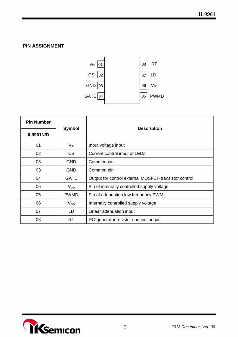
PIN ASSIGNMENT
Pin Number
Symbol Description
IL9961N/D
01 VIN Input voltage input
02 CS Current control input of LEDs
03 GND Common pin
03 GND Common pin
04 GATE Output for control external MOSFET-transistor control
06 VDD Pin of internally controlled supply voltage
05 PWMD Pin of attenuation low frequency PWM
06 VDD Internally controlled supply voltage
07 LD Linear attenuation input
08 RT RC-generator resistor connection pin
01
02
03
04
RTVIN
CS
GND
PWMD
VDD
LD
08
07
06
05GATE

IL9961
2013 December, Ver. 00
Typical Application Circuit
L1 - induction coil 4.7mH VD1 – diode VD2 – LED

IL9961
4 2013 December, Ver. 00
Block Diagram
Regulator
Reset circuit
when turning on
power supply
VINVDD
-
+
CS
LD
1
S
R Q
&
GATE
Rise edge
interlocking
circuit
PWMD
0,15/0,20 V
GND
+
-
Composer
UVLO
Voltage
divider
Average
current control
circuit
+
-0,44 V Q
Delay lineCurrent mirror
circuit
400 s
CLK
RT

IL9961
2013 December, Ver. 00
Absolute Maximum Ratings
Symbol Description Limit Unit Min Max
VIN Input voltage -0.5 470
V
VDD Voltage, applied to the pin VDD -0.3 12.3 V
- Voltage at pin PWMD, CS, LD, GATE, RT
-0.3 VDD + 0.3 V
Тj Maximum Junction Temperature -40 125 °С
* Stresses beyond those listed under “absolute maximum ratings” may cause permanent damage to the device. These are stress ratings only and functional operation of the device at these or any other conditions beyond those indicated under “recommended operating conditions” is not implied. Exposure to absolute-maximum-rated conditions for extended periods may affect device reliability.
Recommended Operating Ratings
Symbol Description
Limit Unit Min Max
VIN Input voltage1) 8 450 V
VDDMAX Maximum voltage, applied to the pin VDD
– 12 V
Тj Maximum Junction Temperature -40 125 °С
PDIS
Dissipated power, in package SO-8
–
6502)
mW
In package SO-16 10002)
1) It is limited by dissipated power in the package 2) Value PDIS is indicated at the ambient temperature of Та ≤ 25 °С
IL9961
6 2013 December, Ver. 00
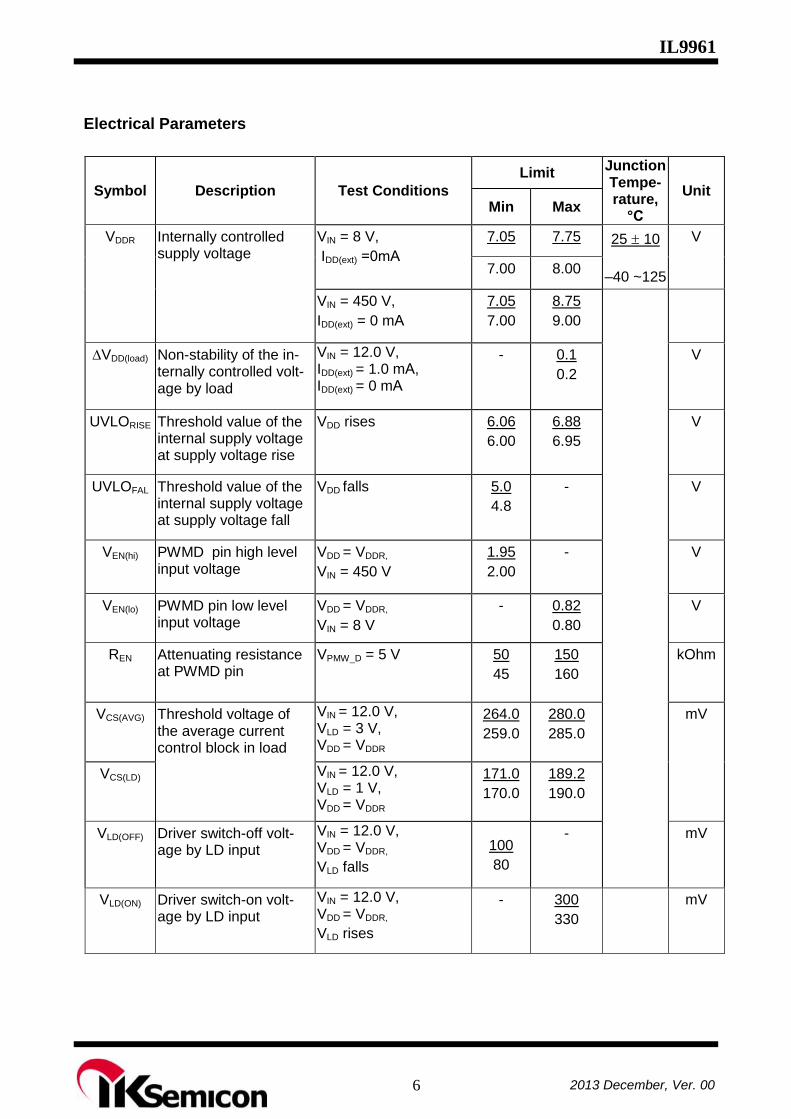
Electrical Parameters
Symbol Description Test Conditions
Limit Junction Tempe-rature,
°С
Unit Min Max
VDDR Internally controlled supply voltage
VIN = 8 V,
IDD(ext) =0mА
7.05 7.75 25 10
–40 ~125
V
7.00 8.00
VIN = 450 V,
IDD(ext) = 0 mА
7.05
7.00
8.75
9.00
∆VDD(load) Non-stability of the in-ternally controlled volt-age by load
VIN = 12.0 V, IDD(ext) = 1.0 mА, IDD(ext) = 0 mА
- 0.1
0.2
V
UVLORISE Threshold value of the internal supply voltage at supply voltage rise
VDD rises 6.06
6.00
6.88
6.95
V
UVLOFAL Threshold value of the internal supply voltage at supply voltage fall
VDD falls 5.0
4.8
- V
VEN(hi) PWMD pin high level input voltage
VDD = VDDR,
VIN = 450 V
1.95
2.00
- V
VEN(lo) PWMD pin low level input voltage
VDD = VDDR,
VIN = 8 V
- 0.82
0.80
V
REN Attenuating resistance at PWMD pin
VPMW_D = 5 V 50
45
150
160
kOhm
VCS(AVG) Threshold voltage of the average current control block in load
VIN = 12.0 V, VLD = 3 V, VDD = VDDR
264.0
259.0
280.0
285.0
mV
VCS(LD) VIN = 12.0 V, VLD = 1 V, VDD = VDDR
171.0
170.0
189.2
190.0
VLD(OFF) Driver switch-off volt-age by LD input
VIN = 12.0 V, VDD = VDDR,
VLD falls
100
80
- mV
VLD(ON) Driver switch-on volt-age by LD input
VIN = 12.0 V, VDD = VDDR,
VLD rises
- 300
330
mV

IL9961
2013 December, Ver. 00
Electrical Parameters continued
Symbol Description Test Conditions
Limit Junction Tempe-rature,
°С
Unit Min Max
VCS(LIM) Threshold voltage of the absolute maxi-mum current control block in load
VDD = VDDR, VIN = 12.0 V
410
390
470
490 25 10
–40~125
mV
ISOURCE GATE pin high level
output current
VDD = 7.5 V, VGATE = 0 V
-165
-100
- mA
ISINK GATE pin low level
output current
VDD = 7.5 V, VGATE = VDD
165
100
- mA
IINsd Consumption current
in off-mode
VIN = 12.0 V, VLD = VDD,
VPWMD = 0 V
- 0.9
1.0
mA
tBLANK
Front edge blanking
time of the current
control
VIN = 12.0 V,
VDD = VDDR 155
150
310
320
ns
tON(MIN)
Driver enable mini-
mum time
VIN = 12.0 V, VDD = VDDR,
VCS = 520 mV
- 1000
1500
ns
tDELAY
Switch-over delay
time of the output
GATE during the si-
nal alteration at the
input CS
VIN = 12.0 V, VDD = VDDR,
VCS = 520 mV
- 150
200
ns
tHICCUP
Driver disable time in
the limit current mode
VIN = 12.0 V, VDD = VDDR, VCS = VDD
330
250
550
650
us
tON(LIM) Driver enable mini-
mum time in absolute
maximum current
mode
VIN = 12.0 V, VDD = VDDR, VCS = VDD
- 430
515
us
tOFF Driver disable time
duration
VIN = 12.0 V, VDD = VDDR, ROSC = 1 mOhm
32
25
48
55
us
VIN = 12.0 V, VDD = VDDR,
ROSC = 226 kOhm
8
6
12
14

IL9961
8 2013 December, Ver. 00
Brief Description of Microcircuit
IL9961 is essentially a LED driver microcircuit, ensuring trimming by average current and
functioning in the mode with the fixed duration of the off-state.
Opposite to the microcircuits with the peak current control the given microcircuit does not
have errors, caused by the difference «peak current – average current». This substantially en-
hances accuracy and efficiency of trimming the LED current during alteration of the supply voltage
or load without necessity to apply the compensation circuits.
Supply of driver IL9961 may be provided from the DC voltage mains of 8 ~ 450 V or the AC
mains rectifier of 85 ~ 265 V.
Average value of output current may be programmed by selecting the various value of the
current metering resistor by the internal (stabilized with the accuracy of ±3 %) reference voltage,
equal to (272 ± 8) mV. It is possible to adjust the mean value of output current, presetting at the
light power linear trimming input the voltage within the range of 0 ~ 1.5 V. The LED dimming ad-
justment is ensured by alteration of the off-duty signal at the input of the PWM-regulator.
Information on Application
Trimming by the peak current of the step-up converter (as in IL9910B) is the most econom-
ic and simple means of adjusting the output current. However, during such adjustment the prob-
lems emerge with the accuracy and stabilization of current due to occurrence of the errors, gener-
ated by the difference «peak current – mean current», which shows up as a result of the current
pulsation in the output inductor and the signal propagation delay in the current reading comparator.
It is also impossible to measure up the continuous signal of the inductor current relative to
the ground in the volt-boosting converter as the power transistor is open only during the small time
periods.
Although it is sufficient to simply detect the peak current at the circuit transistor, trimming by
means of the inductor mean current is usually tied to the current signals relative to voltage VIN.
In IL9961 the appropriate control circuit is used, ensuring the rapid and a very fine trimming
by the average current in the inductor by means of reading the transistor current only. No compen-
sation current trimming circuit is required. Current pulsations in the inductor circuit do not have any
significant influence on this control circuit, and therefore the LED current does not depend on var-
iation of the inductance values, switch-over frequency and output voltage.
Functioning in the mode of the fixed duration of the current off-state in the inductance coil is
used for stabilization and efficiency enhancement of the of LED current trimming in the wide range
of input voltages (opposite of IL9910, the microcircuits IL9961 does not support the operational
mode at the constant frequency).
The type output parameters of the LED driver IL9961 are indicated in Figure 5. For compar-
ison reasons the corresponding parameters of IL9910 are also indicated.

IL9961
2013 December, Ver. 00
Figure 6 – LED Driver IL9961 typical output parameters
Driver’s Operation Description
ICs IL9961 make it possible to control all main types of the key volt-boosting converters,
both with the insulated output and the non-insulated one. When the permitting signal arrives at the
gate of the external MOSFET-transistor, the LED-driver starts to build up the internal energy on the
inductance coil or the transformer’s primary winding, then the given energy, by various ways, de-
pending on the type of the volt-boosting converter, arrives directly to LEDs. The energy, accumu-
lated in the magnetic element, arrives in the output circuit within the time period of switching off the
power MOSFET-transistor, presetting the current in the circuit of LEDs.
With the input supply voltage applied, when the voltage at the pin VDD reaches the thresh-
old value of the internal supply voltage of the low voltage part of the circuit UVLO, the voltage at
the pin GATE rises, and the external MOSFET-transistor switches over to the open state. The val-
ue of output current is controlled by means of limiting by the external MOSFET-transistor the mean
current of the inductance coil. The voltage, falling at the reading resistor, in a serial connection with
the source of the external MOSFET-transistor, arrives at the input CS IC IL9961. When the given
voltage reaches the threshold value of the comparator actuation, the voltage at the pin GATE re-
mains unchanged during the time, equal to the enable time of GATE prior to actuation of the com-
parator. Thus the trimming is ensured by the current mean value. Then the external MOSFET-
transistor switches over to the closed state. The threshold value of the comparator actuation is
preset inside the circuit and constitutes 272 mV or can alter outside by means of applying voltage
at the input LD.
IL9961
10 2013 December, Ver. 00
Input voltage control Supply for driver IL9961 may be realized directly from mains of voltage of direct current
8.0~450 V through pin VIN. When this voltage supplied on pin VIN integrated circuit forms direct
voltage 7.5 V on pin VDD. To pin VDD there should be connected capacitor with small equivalent se-
ries resistance (ESR), in order to provide low resistance of bus for pulses of large current through
GATE pin during integrated circuit operation. IC IL9961 also can be supplied directly through VDD
pin with voltage larger than internally-regulated 7.5 V, but less than 12 V.
Direct voltage supplied on VIN pin, is limited by dissipated power in the package. For exam-
ple, in eight pin SO package at consumption in operating mode of current IIN = 2.5 mA through VIN
pin, maximum direct voltage on VIN pin is calculated by formula (1)
V
IR
TTU
INja
aj
IN 347.
, (1)
where Tj = 125 – maximum operating temperature of chip, OC;
Ta = 25 - ambient temperature, 0C;
Rθ, ja = 148 - thermal resistance of chip - ambient, OC / Watt.
In cases when integrated circuit should operate at higher voltage, sequentially to VIN pin
can be connect resistor or Zener diode for removal of dissipated power from IC. In mentioned ex-
ample, use of 100 V Zener diode allows the scheme to operate up to 447 V. Input current, con-
sumed by integrated circuit through VIN pin is calculated by formula (2)
sGIN fQмАI 0,1 , (2)
where QG - capacity of gate of exterior transistor (from producer specification), pF;
fs - switching frequency, Hz.
LEDs Dimming Control The LEDs dimming control may be performed by two means, separately or in combination,
depending on the application circuit. The LEDs dimming may be controlled either by means of the
linear alteration of the current value via LEDs, or by switching on / off this current at its constant
value. The second adjustment method (the so called MWM-attenuation) is based on LEDs dim-
ming by means of altering the fill-up ratio of the output current pulses.
The linear adjustment of LEDs dimming (linear attenuation) is performed by means of ap-
plying the voltage with the value from 0 to 1.5 V at the input LD. In this case the actuation thresh-
old of the comparator, controlling the voltage at the pin CS, is preset equal to the value: VLD·0.18. It
is in this way, that adjustment of the output current value takes place. The value of the controlled
voltage at the pin CS can be altered by means of the variable resistor, included into the lower
shoulder of the resistive voltage divider of the low voltage part of the circuit VDD and connected to
the pin LD. Application of the voltage over 1.5 V at the input LD does not result in increase of the
preset mean value of the output current. In order to obtain the current of the greater value it is nec-
essary to select the reading resistor with the smaller nominal resistance.

IL9961
2013 December, Ver. 00
VIN1
VDD6
5PWM
7LD
GATE
CS
RT
GND
4
2
8
3R1 R2
Q1
LEDs
Input DC Voltage
C1
22uF
450V
D2
L1U1 IL9961
C2
2.2uF
R3
200kΩ
C3
1uF
R4
50kΩ
IL9961 Linear Dimming Control Schematic
PWM-attenuation is performed by means of application of the external PWM-signal at the pin
PWMD. PWM-signal may be generated by the microcontroller or the pulse generator with the
pulse fill-up ratio, proportionate to the LEDs dimming rate. This signal permits or denies the LEDs
current modulation depending on the pulse shape. In this mode the current value through LEDs
may be in one of two positions: zero or the current nominal value, preset by means of the reading
resistor, connected to the source of the external MOSFET-transistor. Using the given method, it
is impossible to attain the LEDs’ brightness over the value, which is limited by the internally pre-
set threshold of the comparator actuation. When using the PWM-attenuation in operation of IC
IL9961, LEDs’ brightness is adjusted from 0 to 100 %. Accuracy of the PWM-attenuation method
is limited only by the minimum pulse duration, arriving at the gate of the external MOSFET-
transistor, which constitutes fractions of percent from the fill-up ratio of the PWM-signal pulses.

IL9961
12 2013 December, Ver. 00