![January 2018 N`tpsk;gp tUlk;shivaalayam.com/assets/uploads/Calendar2018.pdf · 2018. 6. 25. · \\;b 02:42 tiu gpd; ]g;jkp. Nutjp 18:46 tiu. KOtJk; rpj;jk;. #hpa n[ae;jp uj ]g;jkp](https://static.fdocuments.in/doc/165x107/5fe65a5b1744eb0a7b08648f/january-2018-ntpskgp-tulk-2018-6-25-b-0242-tiu-gpd-gjkp-nutjp-1846.jpg)
IL600 Product Data Sheet - RS Components...
21
IL600 Series IsoLoop ® is a registered trademark of NVE Corporation. *U.S. Patent number 5,831,426; 6,300,617 and others. REV. N NVE Corporation 11409 Valley View Road, Eden Prairie, MN 55344-3617 Phone: (952) 829-9217 Fax: (952) 829-9189 www.IsoLoop.com ©2007 NVE Corporation Passive-Input Digital Isolators – CMOS Outputs Functional Diagrams OUT 1 V OE OUT 1 OUT 2 OUT 1 IN 2 OUT 1 OUT 2 OUT 3 IN 1 IN 1 IN 2 IN 1 OUT 2 IN 1 IN 2 IN 3 V DD1 V DD2 IL610 IL611 IL612 IL613 IL614 OUT 1 IN 2 IN 3 IN 1 OUT 2 OUT 3 COIL RE Features • Up to 100 Mbps Data Rate • Single-ended or Differential Input Operation • Flexible Inputs with Very Wide Input Voltage Range • Failsafe Output (logic high output for zero coil current) • Output Enable (IL610) • 3.3 V or 5 V Operation / Level Translation • 2500 V RMS Isolation (1 minute) • Low Power Dissipation • −40°C to 85°C Temperature Range • 20 kV/μs Transient Immunity • UL1577 and IEC61010 Approvals • 8-Pin MSOP, SOIC, and PDIP Packages • Bare Die Available (IL610) Applications • CAN Bus / Device Net • Differential Line Receiver • Optocoupler Replacement • SPI Interface • RS-485, RS-422, or RS-232 • Digital Fieldbus • Space-critical multi-channel applications Description The IL600 Series are passive input digital signal isolators with CMOS outputs. They have a similar interface but better performance and higher package density than optocouplers. The devices are manufactured with NVE’s patented* IsoLoop ® spintronic Giant Magnetoresistive (GMR) technology for small size, high speed, and low power. A single resistor sets the maximum input current for voltages above 0.5 V. A capacitor in parallel with the current-limit resistor provides improved dynamic performance. These versatile components simplify inventory requirements by replacing a variety of optocouplers and functioning over a wide range of data rates, edge speeds, and power supply levels. The devices are available in MSOP, SOIC, and PDIP packages, as well as bare die.
Transcript of IL600 Product Data Sheet - RS Components...

IL600 Series
IsoLoop® is a registered trademark of NVE Corporation. *U.S. Patent number 5,831,426; 6,300,617 and others.
REV. N
NVE Corporation 11409 Valley View Road, Eden Prairie, MN 55344-3617 Phone: (952) 829-9217 Fax: (952) 829-9189 www.IsoLoop.com ©2007 NVE Corporation
Passive-Input Digital Isolators – CMOS Outputs
Functional Diagrams
OUT1
VOE
OUT1
OUT2
OUT1
IN2
OUT1
OUT2
OUT3
IN1
IN1
IN2
IN1
OUT2
IN1
IN2
IN3
VDD1
VDD2
IL610
IL611
IL612
IL613
IL614
OUT1
IN2
IN3
IN1
OUT2
OUT3
COIL
RE
Features
• Up to 100 Mbps Data Rate • Single-ended or Differential Input Operation • Flexible Inputs with Very Wide Input Voltage Range • Failsafe Output (logic high output for zero coil current) • Output Enable (IL610) • 3.3 V or 5 V Operation / Level Translation • 2500 VRMS Isolation (1 minute) • Low Power Dissipation • −40°C to 85°C Temperature Range • 20 kV/µs Transient Immunity • UL1577 and IEC61010 Approvals • 8-Pin MSOP, SOIC, and PDIP Packages • Bare Die Available (IL610) Applications
• CAN Bus / Device Net • Differential Line Receiver • Optocoupler Replacement • SPI Interface • RS-485, RS-422, or RS-232 • Digital Fieldbus • Space-critical multi-channel applications Description
The IL600 Series are passive input digital signal isolators with CMOS outputs. They have a similar interface but better performance and higher package density than optocouplers.
The devices are manufactured with NVE’s patented* IsoLoop® spintronic Giant Magnetoresistive (GMR) technology for small size, high speed, and low power.
A single resistor sets the maximum input current for voltages above 0.5 V. A capacitor in parallel with the current-limit resistor provides improved dynamic performance.
These versatile components simplify inventory requirements by replacing a variety of optocouplers and functioning over a wide range of data rates, edge speeds, and power supply levels. The devices are available in MSOP, SOIC, and PDIP packages, as well as bare die.
IL600 Series
2
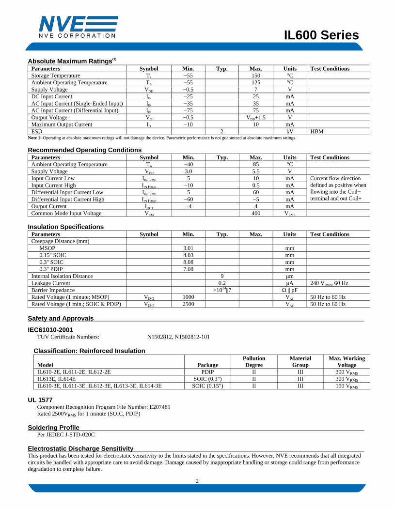
Absolute Maximum Ratings(1) Parameters Symbol Min. Typ. Max. Units Test Conditions Storage Temperature TS −55 150 °C Ambient Operating Temperature TA −55 125 °C Supply Voltage VDD −0.5 7 V DC Input Current IIN −25 25 mA AC Input Current (Single-Ended Input) IIN −35 35 mA AC Input Current (Differential Input) IIN −75 75 mA Output Voltage VO −0.5 VDD+1.5 V Maximum Output Current IO −10 10 mA ESD 2 kV HBM
Note 1: Operating at absolute maximum ratings will not damage the device. Parametric performance is not guaranteed at absolute maximum ratings.
Recommended Operating Conditions Parameters Symbol Min. Typ. Max. Units Test Conditions Ambient Operating Temperature TA −40 85 °C Supply Voltage VDD 3.0 5.5 V Input Current Low IIN LOW 5 10 mA Input Current High IIN HIGH −10 0.5 mA Differential Input Current Low IIN LOW 5 60 mA Differential Input Current High IIN HIGH −60 −5 mA
Current flow direction defined as positive when flowing into the Coil− terminal and out Coil+
Output Current IOUT −4 4 mA Common Mode Input Voltage VCM 400 VRMS
Insulation Specifications
Parameters Symbol Min. Typ. Max. Units Test Conditions Creepage Distance (mm) MSOP 3.01 mm 0.15'' SOIC 4.03 mm 0.3'' SOIC 8.08 mm 0.3'' PDIP 7.08 mm Internal Isolation Distance 9 μm Leakage Current 0.2 μA 240 VRMS, 60 Hz Barrier Impedance >1014||7 Ω || pF Rated Voltage (1 minute; MSOP) VISO 1000 VAC 50 Hz to 60 Hz Rated Voltage (1 min.; SOIC & PDIP) VISO 2500 VAC 50 Hz to 60 Hz
Safety and Approvals
IEC61010-2001 TUV Certificate Numbers: N1502812, N1502812-101
Classification: Reinforced Insulation
Model Package Pollution Degree
Material Group
Max. Working Voltage
IL610-2E, IL611-2E, IL612-2E PDIP II III 300 VRMS IL613E, IL614E SOIC (0.3") II III 300 VRMS IL610-3E, IL611-3E, IL612-3E, IL613-3E, IL614-3E SOIC (0.15") II III 150 VRMS
UL 1577
Component Recognition Program File Number: E207481 Rated 2500VRMS for 1 minute (SOIC, PDIP)
Soldering Profile
Per JEDEC J-STD-020C Electrostatic Discharge Sensitivity This product has been tested for electrostatic sensitivity to the limits stated in the specifications. However, NVE recommends that all integrated circuits be handled with appropriate care to avoid damage. Damage caused by inappropriate handling or storage could range from performance degradation to complete failure.
IL600 Series
3
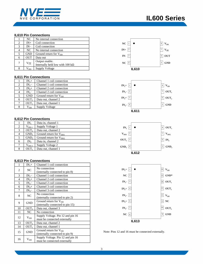
IL610 Pin Connections
1 NC No internal connection 2 IN+ Coil connection 3 IN− Coil connection 4 NC No internal connection 5 GND Ground return for VDD 6 OUT Data out
7
VOE Output enable. Internally held low with 100 kΩ
8 VDD Supply Voltage
IL610
IL611 Pin Connections 1 IN1+ Channel 1 coil connection 2 IN1− Channel 1 coil connection 3 IN2+ Channel 2 coil connection 4 IN2− Channel 2 coil connection 5 GND Ground return for VDD 6 OUT2 Data out, channel 2 7 OUT1 Data out, channel 1 8 VDD Supply Voltage
IL611
IL612 Pin Connections 1 IN1 Data in, channel 1 2 VDD 1 Supply Voltage 1 3 OUT2 Data out, channel 2 4 GND1 Ground return for VDD1 5 GND2 Ground return for VDD2 6 IN2 Data in, channel 2 7 VDD 2 Supply Voltage 2 8 OUT1 Data out, channel 1
IL612
IL613 Pin Connections 1 IN1+ Channel 1 coil connection
2 NC No connection (internally connected to pin 8)
3 IN1− Channel 1 coil connection 4 IN2+ Channel 2 coil connection 5 IN2− Channel 2 coil connection 6 IN3+ Channel 3 coil connection 7 IN3− Channel 3 coil connection
8 NC No connection (internally connected to pin 2)
9 GND Ground return for VDD (internally connected to pin 15)
10 OUT3 Data out, channel 3 11 NC No connection
12 VDD Supply Voltage. Pin 12 and pin 16 must be connected externally
13 OUT2 Data out, channel 2 14 OUT1 Data out, channel 1
15 GND Ground return for VDD (internally connected to pin 9)
16 VDD Supply Voltage. Pin 12 and pin 16 must be connected externally
IL613 Note: Pins 12 and 16 must be connected externally.
NC VDD
IN+ VOE
IN- OUT
NC GND
IN1+ VDD
IN1- OUT1
IN2+ OUT2
IN2- GND
IN1+ VDD
NC GND*
IN1- OUT1
IN2+ OUT2
IN2- VDD
IN3+
IN3-
NC
OUT3
NC GND
IN1 OUT1
VDD1 VDD2
OUT2 IN2
GND1 GND2

IL600 Series
4
IL614 Pin Connections
1 VDD1 Supply Voltage 1
2 GND1 Ground return for VDD1 (internally connected to pin 8)
3 OUT1 Data out, channel 1
4 RE Channel 1 data output enable. Internally held low with 100 kΩ
5 IN2 Data in, channel 2
6 Vcoil Supply connection for channel 2 and channel 3 coils
7 IN3 Data in, channel 3
8 GND1 Ground return for VDD1 (internally connected to pin 2)
9 GND2 Ground return for VDD2 (internally connected to pin 15)
10 NC No Connection 11 OUT3 Data out, channel 3 12 VDD2 Supply Voltage 2 13 OUT2 Data out, channel 2 14 IN1+ Coil connection
15 GND2 Ground return for VDD2 (internally connected to pin 9)
16 IN1− Coil connection
IL614
VDD1 IN1-
GND1 GND2
OUT1 IN1+
RE OUT2
IN2 VDD2
VCOIL
IN3 NC
OUT3
GND1 GND2

IL600 Series
5
Electrical Specifications Electrical specifications are Tmin to Tmax and 4.5 V to 5.5 V unless otherwise stated.
Parameters Symbol Min. Typ. Max. Units Test Conditions
Coil Input Impedance ZCOIL 47||8 78||9 87||10 Ω||nH TAMB = 25°C VDD = 3.0 V to 5.5 V
Temperature Coefficient of Coil Resistance TC RCOIL 0.2 0.25 Ω/°C VDD = 3.0 V to 5.5 V
Input Threshold for Output Logic High IINH 0.5 1 mA Single or Differential VDD = 3.0 V to 5.5 V
Single-ended Input Threshold for Output Logic Low IINL 5 3.5 mA VDD = 3.0 V to 5.5 V
Differential Input Threshold for Output Logic Low IINL 5 3.5 mA VDD = 3.0 V to 5.5 V
Quiescent Current
IL610, IDD IL611, IDD IL612, IDD1 IL612, IDD2 IL613, IDD IL614, IDD1 IL614, IDD2
2 4 2 2 6 2 4
3 6 3 3 9 3 6
mA mA mA mA mA mA mA
VDD = 5 V, IIN = 0
4.9 5 V VDD = 5 V, IO = 20 μA Logic High Output Voltage VOH 4.0 4.8 VDD = 5 V, IO = 4 mA
0 0.1 V VDD = 5 V, IO = −20 μA Logic Low Output Voltage VOL 0.2 0.8 VDD = 5 V, IO = −4 mA
Logic Output Drive Current |IO| 7 10 mA IFS-HIGH −25 0.5 mA Failsafe Operation Input Current(4) IFS-LOW 5 25 mA See Test Circuit 1
Switching Specifications at 5V Input Signal Rise and Fall Times tIR, tIF 1 μs See Test Circuit 1 Data Rate 100 Mbps See Test Circuit 1 Minimum Pulse Width(1) PW 10 ns See Test Circuit 1 Propagation Delay Input to Output (High-to-Low) tPHL 8 15 ns See Test Circuit 1
Propagation Delay Input to Output (Low to High) tPLH 8 15 ns See Test Circuit 1
Average Propagation Delay Drift tPLH 10 ps/°C Pulse Width Distortion |tPHL−tPLH| (2) PWD 3 5 ns See Test Circuit 1 Propagation Delay Skew(3) tPSK −2 2 ns See Test Circuit 1 Output Rise Time (10–90%) tR 2 4 ns See Test Circuit 1 Output Fall Time (10–90%) tF 2 4 ns See Test Circuit 1 Common Mode Transient Immunity |CMH|,|CML| 15 20 kV/μs VT = 300 Vpeak
Notes:
1. Minimum Pulse Width is the shortest pulse width at which the specified PWD is guaranteed. 2. PWD is defined as | tPHL − tPLH |. 3. tPSK is equal to the magnitude of the worst case difference in tPHL and/or tPLH that will be seen between units at 25°C. 4. Failsafe Operation is defined as the guaranteed output state which will be achieved if the DC input current falls between the input levels specified
(see Test Circuit for details).

IL600 Series
6
Electrical specifications are Tmin to Tmax and 3.0V to 3.6V unless otherwise stated. Parameters Symbol Min. Typ. Max. Units Test Conditions
Quiescent Current
IL610, IDD IL611, IDD IL612, IDD1 IL612, IDD2 IL613, IDD IL614, IDD1 IL614, IDD2
1.3 2.6 1.3 1.3 4
1.3 2.6
2 4 2 2 6 2 4
mA mA mA mA mA mA mA
VDD = 3.3 V, IIN = 0
3.2 3.3 V VDD = 3.3 V, IO = 20 μA Logic High Output Voltage VOH 3.0 3.1 VDD = 3.3 V, IO = 4 mA 0 0.1 V VDD = 3.3 V, IO = −20 μA Logic Low Output Voltage VOL 0.2 0.8 VDD = 3.3 V, IO = −4 mA
Logic Output Drive Current |IO| 7 10 mA IFS-HIGH −25 0.3 mA Failsafe Operation Input Current(4) IFS-LOW 8 25 mA See Test Circuit 1
Switching Specifications at 3.3V Input Signal Rise and Fall Times tIR, tIF 1 μs See Test Circuit 1 Data Rate 100 Mbps See Test Circuit 1 Minimum Pulse Width(1) PW 10 ns See Test Circuit 1 Propagation Delay Input to Output (High to Low) tPHL 12 18 ns See Test Circuit 1
Propagation Delay Input to Output (Low to High) tPLH 12 18 ns See Test Circuit 1
Average Propagation Delay Drift tPLH 10 ps/°C Pulse Width Distortion |tPHL−tPLH| (2) PWD 3 5 ns See Test Circuit 1 Propagation Delay Skew(3) tPSK −2 2 ns See Test Circuit 1 Output Rise Time (10–90%) tR 3 5 ns See Test Circuit 1 Output Fall Time (10–90%) tF 3 5 ns See Test Circuit 1 Common Mode Transient Immunity |CMH|,|CML| 15 20 kV/μs VT = 300 Vpeak
Notes:
1. The Minimum Pulse Width is the shortest pulse width at which the specified PWD is guaranteed. 2. PWD is defined as | tPHL − tPLH |. 3. tPSK is equal to the magnitude of the worst case difference in tPHL and/or tPLH that will be seen between units at 25°C. 4. Failsafe Operation is defined as the guaranteed output state which will be achieved if the DC input current falls between the input levels specified
(see Test Circuit 1 for details). Note if Failsafe to Logic Low is required, the DC current supplied to the coil must be at least 8 mA using 3.3 V supplies versus 5 mA for 5 V supplies. Select the value of limit resistor appropriately.

IL600 Series
7
Test Circuits
The test circuits below were used to obtain the specifications on the previous pages. In differential mode, the boost capacitor is generally not required, but it may be used to increase external magnetic field immunity or improve PWD performance as required.
+V VDD
GND1 GND2
3
25
6
7
8
-+
1K
15 pF
10 nF
Rlimit
Cboost
GND11 2
1K
IL610
+V VDD
GND1 GND2
3
25
6
7
8
-+
1K
15 pF
10 nF
GND11 2
1K
IL610Rlimit
Test Circuit 1 (Single-Ended) Test Circuit 2 (Differential) Operation
IL600-Series Isolators are current mode devices. Changes in current flow into the input coil result in logic state changes at the output. One of the significant advantages of the passive coil input is that both single ended and differential inputs can be handled without reverse bias protection. The GMR sensor switches the output to logic low if current flows from (In−) to (In+). Resistors set the coil input current to the 5 mA minimum. There is no limit to input voltages because there are no semiconductor input structures.
The absolute maximum current through the coil of the IL600-Series is 25 mA DC, or ±75 mA in differential mode. The worst-case logic low threshold current is 5 mA. While typical threshold currents are actually less, NVE recommends 5 mA logic low thresholds as a minimum design value. In all cases, the current must flow from In− to In+ in the coil to switch the output low. This is the case for true or inverted data, in single-ended or differential configurations. Output logic high is the zero input current state. Note that current flowing from Coil+ to Coil- (negative current in the specifications) will push the GMR sensor further into the high state.
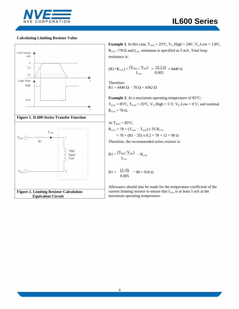
Figure 1 shows the response of the IL600-Series. The GMR bridge structure is designed so the output of the isolator is logic high with no signal present. The output will switch to the low state with approximately 3.5 mA of coil current, and switch back to the high state when the input current falls below 1.5 mA. This allows glitch-free interface with low slew rate signals.
To calculate the value of the protection resistor (R1), use Ohm’s law as shown in the examples below. Note that only the magnitude of the voltage across the coil is important; the absolute values of VINH and VINL are arbitrary.
IL600 Series
8
Calculating Limiting Resistor Value Example 1. In this case, TNOM = 25ºC, VIN High = 24V, VIN Low = 1.8V, RCOIL =78 Ω and ICOIL minimum is specified as 5 mA. Total loop resistance is:
(R1+RCOIL) = (VINH − VINL) = 22.2 Ω = 4440 Ω ICOIL 0.005 Therefore: R1 = 4440 Ω − 78 Ω = 4362 Ω Example 2. At a maximum operating temperature of 85°C: TMAX = 85ºC, TNOM = 25ºC, VIN High = 5 V, VIN Low = 0 V, and nominal RCOIL = 78 Ω. At TMAX = 85ºC: RCOIL = 78 + (TMAX − TMIN) x TCRCOIL = 78 + (85 − 25) x 0.2 = 78 + 12 = 90 Ω Therefore, the recommended series resistor is:
R1 = (VINH−VINL) – RCOIL
ICOIL
R1 = (5−0) − 90 = 910 Ω 0.005 Allowance should also be made for the temperature coefficient of the current limiting resistor to ensure that ICOIL is at least 5 mA at the maximum operating temperature.
3.5
5
High
Low
Logic State
Coil CurrentmA
1.5
t
t Figure 1. IL600-Series Transfer Function
VINH
VINL
ICOIL
R1
78InputCoil
Figure 2. Limiting Resistor Calculation Equivalent Circuit

IL600 Series
9
250016 5000
3
500
1000
SignalRise/Fall Time (ns)
CBoost (pF)
250016 5000
3
500
1000
SignalRise/Fall Time (ns)
CBoost (pF)
Failsafe Operation
Internal failsafe biasing ensures the output will always switch to the high state if the input coil is open-circuit. This is true for either 5 V or 3.3 V output supplies. The specifications on pages 5 and 6 show the enhanced failsafe conditions available with the IL600-Series Isolators that cover the non-open circuit condition. The output will remain in the state specified, or will switch to that state, if the specified current is flowing in the coil. Note that positive values of current mean current flow into the In− input (pin 3 in Test Circuit 1). Single-Ended or Differential Input
The IL610, IL611, IL613, and channel 1 of the IL614 can be run with single-ended or differential inputs. In differential mode, coil current reverses each cycle. In single-ended mode, a “boost capacitor” placed across the current limit resistor provides pulsed current reversal for correct operation. In the differential mode, current will naturally flow through the coil in both directions without the boost cap, although the cap can still be used if application factors such as increased external field immunity or improved PWD performance mandate. Absolute Maximum recommended coil current in single-ended mode is 25 mA while differential mode allows up to ±75 mA to flow. The difference in specifications is due to the risk of electromigration of coil metals under constant current flow. In single ended mode, long-term DC current flow above 25 mA can cause erosion of the coil metal (rather like river flow does to its banks). In differential mode, erosion takes place in both directions as each current cycle reverses and has a net effect of zero up to the fuse current. A current of more than 100 mA will cause the coil to irreparably fuse open.
There are many applications where the differential option can be very useful. One advantage over optocouplers and other high-speed couplers is that no reverse bias protection for the input structure is required for a differential signal. This reduces cost and complexity. One of the more common applications is for an isolated Differential Line Receiver. For example, RS-485 can drive an IL610 directly for a fraction of the cost of an isolated RS-485 node (see Illustrative Applications section). Typical Resistor Values
The table shows typical values for the external resistor in 5 V and 3 V logic systems. As always, these values as approximate and should be adjusted for temperature or other application specifics If the expected temperature range is large, 5% or even 1% tolerance resistors may provide additional design margin. Alternatively, see the
Applications Information section for circuit ideas allowing more generalized resistor selection. Boost Capacitor
The boost capacitor in parallel with the current-limiting resistor boosts the instantaneous coil current at the signal transition. The boost pushes the GMR bridge output through the comparator threshold voltage with less propagation delay and pulse width distortion. The instantaneous boost capacitor current is proportional to input edge speeds ( ). Select a capacitor value based on the rise and fall times of the input signal to be isolated that provides approximately 20 mA of additional “boost” current. Figure 3 is a guide to boost capacitor selection. For standard logic signals (tr,tf < 10 ns), a 16 pF capacitor is recommended. The capacitor value is generally not critical, and can often vary ±50% with little noticeable difference in device performance.
Dynamic Power Consumption
Power consumption is proportional to duty cycle, not data rate. The use of NRZ coding minimizes power dissipation since no additional power is consumed when the output is in the high state. In differential mode, where the logic high condition may still require a current to be forced through the coil, power consumption will be higher than a typical NRZ single ended configuration.
Power Supply Decoupling
47 nF ceramic capacitors are recommended to decouple the power supplies. The capacitors should be placed as close as possible to the appropriate VDD pin for optimal output wave shaping.
VCOIL 0.125W, 10% Resistor 3.3 V 560 Ω 5 V 910 Ω
Figure 3. Cboost Selector
dV dt C

IL600 Series
10
Applications Information
IL600-Series Isolators are current mode devices. This means that a current of a certain magnitude and direction must flow in the input coil to change the output logic state. Figure 4 shows a simplified transfer curve for a typical IL600-Series data channel.
The transfer function for this device is approximately linear. An applied coil input current creates a magnetic field that causes the GMR bridge output to change in proportion to the applied field. The GMR bridge is connected to a comparator. When the bridge output is greater than the comparator high threshold level, the output will go high. Similarly, when the bridge output is less than the comparator low threshold, the output will go low. The “Window of Operation” shown in Figure 4 highlights the specified corners of device operation. An input current
of approximately −3.5 mA or −1.5 mA will cause the device to hover around the comparator switching thresholds producing an unstable output. For single-ended operation across the entire temperature range and power supply range, the magnitude of the coil current for a logic low should be at least −5 mA, and the magnitude of the coil current for a logic high should be between −0.5 mA and 0 mA. The stated direction of the current is negative in Figure 4 because the magnetic field is negative with respect to Earth Field. Current is always fed into the In− terminal of an IL600-Series device. Since these currents are actually sourced, not sunk by the user, the specified currents are quoted as positive values in the Electrical Specifications section of this data sheet.
When designing circuits using digital logic, most designers are aware that the input to a logic gate is differential with respect to ground. Separate ground layers, star points or planes usually need to be designed into circuit boards with fast switching currents to reduce ground voltage bounce caused by inductance in ground returns. Ground error voltages can cause data errors in high-speed circuits due to their impact on the effective logic threshold voltage at any given instant. Similarly, when using IL600-Series devices, the designer should be aware that it is the voltage magnitude across the coil that creates the current, not just the value of the input voltage. To illustrate this point, consider the single-ended non-inverting and inverting cases.
Coil Current (mA)
Bridge o/p (mV)
Comparator Low Threshold
Comparator High Threshold
-7 -6 -5 -4 -3 -2 -1 0 -10 -9 -8
-40 -20
60
40
20
105
Window of Operation
-60
Bridge Output Response
Figure 4. IL600-Series Transfer Function

IL600 Series
11
In the non-inverting circuit, the In− terminal is connected via a 1 kΩ current-limiting resistor to the supply rail, and the input is connected to the In+ terminal. Assume the supply voltage is +5 V and the input signal is a 5 V CMOS signal. A 1 kΩ resistance is selected to limit the coil current to 5 mA. For the purpose of this illustration we will ignore the coil resistance. When a logic high (+5 V) is applied to the input, the current through the coil is zero. When the input is a logic low (0 V), approximately 5 mA flows through the coil from the In− side to the In+ side. Figure 4 shows that the device will transition to both logic states easily under these conditions. Now assume that the 5 V rail is at 5.5 V and the CMOS input signal is loaded so that its high level is only 4.5 V. When a logic high (4.5 V) appears on the input, there is still a current of −1mA flowing through the coil. Figure 4 shows that the device is getting close to the off-state threshold of −1.5 mA, and now exceeds the specification of −0.5 mA for this logic level. Some intermittent operation or complete non-function should be expected in this case. The designer must ensure that the difference between the logic high voltage and the power supply voltage is such that the residual current in the coil is lower than 0.5 mA.
The inverting configuration design problem is similar to the problems associated with standard logic. In the inverting configuration, the signal into the coil is differential with respect to ground. The designer must ensure that the difference between the logic low voltage and the coil ground is such that the residual coil current is less than 0.5 mA. Conventional ground bounce design precautions apply.
The IL612 and IL614 devices have some inputs that do not offer inverting operation. The IL612 coil In− input is hardwired internally to the device power supply; therefore it is important to ensure the isolator power supply is at the same voltage as the power supply to the source of the input logic signal. The IL614 has a common coil In− for two inputs. This pin should be connected to the power supply for the logic driving channels 2 and 3, and the channels run should be run in non-inverting mode.
IL600 devices are simple to use as long as it is remembered that there must be enough coil current (5 mA) to ensure logic low output, and close to zero current (0.5 mA to 0 mA) to ensure logic high output.
VDD
GND2
5
6
78
Note. C1 is 47 nF ceramic.Non-Inverting Circuit
Data Out
C1
1
+5 V
GND1
1K
3
2
Data In
Cboost
IL610
-+
+5 V VDD
GND1 GND2
1K3
25
6
8
Note. C1 is 47 nF ceramic.
IL610
Inverting Circuit
-+
Data In
Data Out
7C1
Cboost
Figure 5. Inverting and non-inverting circuits

IL600 Series
12
Magnetic Field Immunity
IsoLoop devices operate by imposing a magnetic field on a GMR sensor, which translates the change in field into a change in logic state. The devices are manufactured with a magnetic shield above the sensor. The shield acts as a flux concentrator to boost the magnetic signal from the internal coil, and as a shield against external magnetic fields. The shield absorbs surrounding stray flux until it becomes saturated. At saturation the shield is transparent to external applied fields, and the GMR sensor may react to the field. To compensate for this effect, IsoLoop Isolators use Wheatstone Bridge structures that are only sensitive to differential magnetic fields.
There are several ways of enhancing magnetic field immunity. Providing a larger internal field will reduce the effect of an external field on the GMR sensor.
Immunity to external magnetic fields can also be enhanced by proper orientation of the device with respect to the field direction, the use of differential signaling, and field boosting capacitors.
Two ways to enhance immunity to external magnetic field are summarized below.
1. Orientation of the device with respect to the field direction
An applied field in the “H1” direction is the worst case for magnetic immunity. In this case the external field is in the same direction as the applied internal field. In one direction it will tend to help switching; in the other it will hinder switching. This can cause unpredictable operation.
An applied field in direction “H2” has considerably less effect and results in higher magnetic immunity.
NC VDD
IN+ VOE
IN- OUT
NC GND
2. Differential Signaling and Boost Capacitors
Regardless of orientation, driving the coil differentially improves magnetic immunity. This is because the logic high state is driven by an applied field instead of zero field, as is the case with single-ended operation. The higher the coil current, the higher the internal field, and the higher the immunity to external fields. Optimal magnetic immunity is achieved by adding the boost capacitor.
Method Approximate Immunity Immunity Description
Field applied in H1 direction ±20 Gauss A DC current of 16 A flowing in a conductor 1 cm from the device could cause disturbance.
Field applied in H2 direction ±70 Gauss A DC current of 56 A flowing in a conductor 1 cm from the device could cause disturbance.
Field applied in any direction but with field booster capacitor (16 pF) in circuit ±250 Gauss A DC current of 200 A flowing in a conductor
1 cm from the device could cause disturbance.
Data Rate and Magnetic Field Immunity
It is easier to disrupt an isolated DC signal with an external magnetic field than it is to disrupt an isolated AC signal. Similarly, a DC magnetic field will have a greater effect on the device than an AC magnetic field of the same effective magnitude. For example, signals with pulses greater than 100 μs long are more susceptible to magnetic fields than shorter pulse widths.
H1 H2
IL600 Series
13
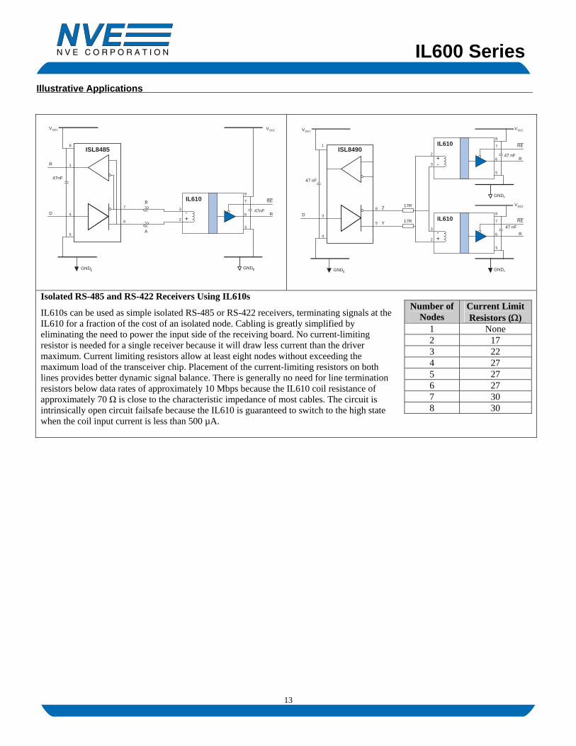
Illustrative Applications
GND2
VDD2
B
ISL8485
D
47nF
VDD1
GND1
3
2
5
6
7
8
4
5
7
21
-+
IL610
R
RE
A
8
6
1R
47nF
GND3
VDD2
Z
ISL8490
D
47 nF
VDD1
GND1
3
2
5
6
7
83
4
6
47 nF
1
-+
IL610
R
REY
1
5
2
3
5
6
7
8
+-
IL610
R
RE
47 nF
VDD3
GND2
17R
17R
Isolated RS-485 and RS-422 Receivers Using IL610s
IL610s can be used as simple isolated RS-485 or RS-422 receivers, terminating signals at the IL610 for a fraction of the cost of an isolated node. Cabling is greatly simplified by eliminating the need to power the input side of the receiving board. No current-limiting resistor is needed for a single receiver because it will draw less current than the driver maximum. Current limiting resistors allow at least eight nodes without exceeding the maximum load of the transceiver chip. Placement of the current-limiting resistors on both lines provides better dynamic signal balance. There is generally no need for line termination resistors below data rates of approximately 10 Mbps because the IL610 coil resistance of approximately 70 Ω is close to the characteristic impedance of most cables. The circuit is intrinsically open circuit failsafe because the IL610 is guaranteed to switch to the high state when the coil input current is less than 500 µA.
Number of Nodes
Current Limit Resistors (Ω)
1 None 2 17 3 22 4 27 5 27 6 27 7 30 8 30

IL600 Series
14
SJA1000
PCA82C250
1
2
3
4 5
6
7
8Rs
CANH
CANL
Vref
TXD
GND
Vcc
RXD
1
2
3
4 5
6
14
13
12
8
15
18
19
20
21
22
VSS3
VSS2VSS1
VDD3
VDD2
VDD1
TX0
TX1
RX1
RX0
VDD2VDD1
GND2GND1
C6
C5
C4
C3
C2
C1
Rs
1K
1K
Cboost
Cboost
78
4
Notes: C
boost is 16 pF ceramic
All other capacitors are 47 nF ceramic
VDD1
VDD2
IL612
Isolated CAN Bus
Low pulse width distortion is critical for CAN bus, and IL600 Isolators are specified for just 3 ns typical pulse width distortion. Their fail-safe output (logic high output for zero coil current) ensures proper power-on. The speed of IL600 isolators easily supports the maximum CAN bus transfer speed of 1 Mbps.
IL600 Series
15
GND2GND1
VDD2VDD1
A
B
1
2
4
3
5
6
8
7
390R
390R
220R
ISL8487E
R
RE
DE
D
C3123
4
5
6
78 9
10
11
12
13
14
15
16C1
C2
1K
1K
D
DE
R
RE
-
-
+
+
-+
Cboost
Cboost
Cboost
RE
IL614
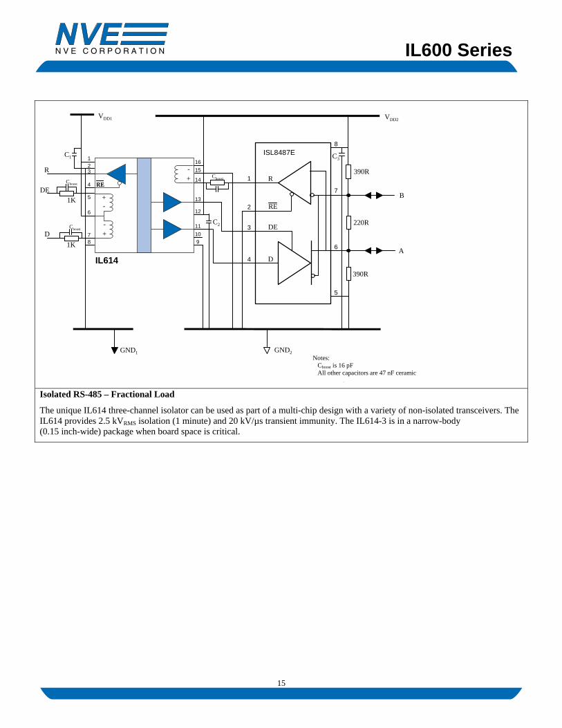
Notes: Cboost is 16 pF All other capacitors are 47 nF ceramic
Isolated RS-485 – Fractional Load
The unique IL614 three-channel isolator can be used as part of a multi-chip design with a variety of non-isolated transceivers. The IL614 provides 2.5 kVRMS isolation (1 minute) and 20 kV/µs transient immunity. The IL614-3 is in a narrow-body (0.15 inch-wide) package when board space is critical.
Cboost is 16 pF ceramic . All other capacitors are 47 nF ceramic
Notes: Cboost is 16 pF All other capacitors are 47 nF ceramic
IL600 Series
16
-+
-+
3
2
3
21K
1K
IL610
LM309H
IR2102
5
6
8
8
6
5
1
2
3
4 5
6
7
8
+5 V 10-20 V 600 V max.
12
3
LIN
Hi-Drive
Lo-Drive
To Load
C1
C2
HIN HO
LO
VS
VCC VB
COM
GND1 GND2
Cboost
Cboost
CAPP-+
-+ 5
.
1
2
boost
Notes: Cboost is 16 pF CAPP is application specific All other capacitors are 47 nF ceramic
IL610
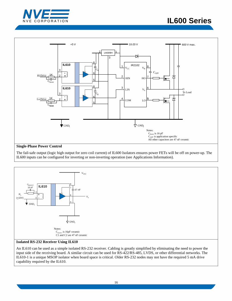
Single-Phase Power Control
The fail-safe output (logic high output for zero coil current) of IL600 Isolators ensures power FETs will be off on power-up. The IL600 inputs can be configured for inverting or non-inverting operation (see Applications Information).
GND
VDD2
GND
CBOOST
3
2
5
6
7
8
47 nF
2
1
-+
IL610
Vo
16 pF
Rx
(+10V)_
Isolated RS-232 Receiver Using IL610
An IL610 can be used as a simple isolated RS-232 receiver. Cabling is greatly simplified by eliminating the need to power the input side of the receiving board. A similar circuit can be used for RS-422/RS-485, LVDS, or other differential networks. The IL610-1 is a unique MSOP isolator when board space is critical. Older RS-232 nodes may not have the required 5 mA drive capability required by the IL610.
Notes: C
BOOST is 16pF ceramic
C1 and C2 are 47 nF ceramic

IL600 Series
17
Package Drawings, Dimensions and Specifications 8-pin MSOP
0.114 (2.90)
0.114 (2.90)
0.016 (0.40)
0.005 (0.13)0.009 (0.23)
0.027 (0.70)
0.010 (0.25)
0.018 (0.45)
0.002 (0.05)
0.043 (1.10)0.032 (0.80)
0.006 (0.15)
0.016 (0.40)
0.022 (0.55)
0.189 (4.80)0.197 (5.00)
0.122 (3.10)
0.122 (3.10)
6˚
0˚
8-pin SOIC Package
8-pin PDIP
0.355 (9.02)0.400 (10.16)

IL600 Series
18
0.15" 16-pin SOIC Package
0.054 (1.4)0.072 (1.8)
0.040 (1.0)0.060 (1.5)
0.016 (0.4)0.050 (1.3)
0.386 (9.80)0.394 (10.00)
Pin 1 identified by either an indent or a marked dot
NOM
0.228 (5.79)0.244 (6.20)
0.152 (3.86)0.157 (3.99)
Dimensions in inches (mm)
0.007 (0.2)0.013 (0.3)
0.004 (0.1)0.012 (0.3)
0.040 (1.02)0.050 (1.27)
0.013 (0.3)0.020 (0.5)
0.3" 16-pin SOIC Package
NOM
Pin 1 identified by either an indent or a marked dot
0.287 (7.29)0.300 (7.62)
Dimensions in inches (mm)
0.08 (2.0)0.10 (2.5)
0.092 (2.34)0.105 (2.67)
0.397 (10.08)0.413 (10.50)
0.013 (0.3)0.020 (0.5)
0.394 (10.00)0.419 (10.64)
0.040 (1.0)0.060 (1.5)
0.004 (0.1)0.012 (0.3)
0.007 (0.2)0.013 (0.3)
0.016 (0.4)0.050 (1.3)
IL600 Series
19
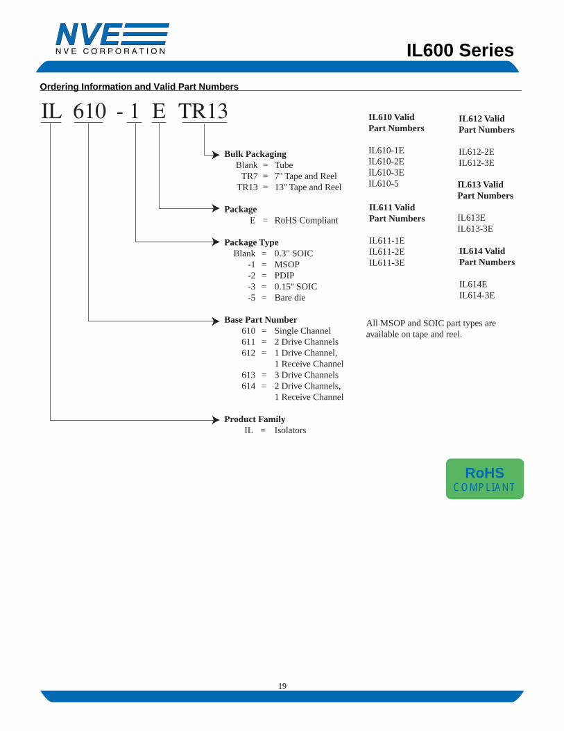
Ordering Information and Valid Part Numbers
Bulk Packaging Blank = Tube TR7 = 7'' Tape and Reel TR13 = 13'' Tape and Reel
PackageE = RoHS Compliant
Package Type Blank = 0.3" SOIC
-1 = MSOP -2 = PDIP -3 = 0.15'' SOIC -5 = Bare die
Base Part Number 610 = Single Channel 611 = 2 Drive Channels
612 = 1 Drive Channel, 1 Receive Channel 613 = 3 Drive Channels 614 = 2 Drive Channels, 1 Receive Channel
Product Family IL = Isolators
IL610 Valid Part Numbers
IL610-1EIL610-2EIL610-3EIL610-5
IL611 Valid Part Numbers
IL611-1EIL611-2EIL611-3E
IL612 Valid Part Numbers
IL612-2EIL612-3E
IL613 Valid Part Numbers
IL613E IL613-3E
IL614 Valid Part Numbers
IL614EIL614-3E
All MSOP and SOIC part types are available on tape and reel.
RoHSCOMPLIANT

IL600 Series
20
Revision History ISB-DS-001-IL600-N December 2007
Changes • Change lower limit of length on PDIP package drawing.
ISB-DS-001-IL600-M
Changes • Changed ordering information to reflect that devices are now fully RoHS compliant with
no exemptions.
ISB-DS-001-IL600-L
Changes • Added differential drive specifications
• Eliminated soldering profile chart
ISB-DS-001-IL600-K
Changes • Changed IL485 transceiver
ISB-DS-001-IL600-J
Changes • Added enhanced failsafe specification
• Repaginated
ISB-DS-001-IL600-I
Changes • New 16-pin package drawings
• Replaced RS232 application with simple receiver
• Minor changes to application schematics
• Expanded captions for illustrative applications
ISB-DS-001-IL600-H
Changes • Misc. typographical and syntax changes
ISB-DS-001-IL600-G
Changes • Voltage ratings added to Insulation Specifications
• Notes added on use of Cboost
• 5 V specifications without Cboost removed
• Test Circuit #2 removed

IL600 Series
21
About NVE An ISO 9001 Certified Company
NVE Corporation manufactures innovative products based on unique spintronic Giant Magnetoresistive (GMR) technology. Products include Magnetic Field Sensors, Magnetic Field Gradient Sensors (Gradiometers), Digital Magnetic Field Sensors, Digital Signal Isolators, and Isolated Bus Transceivers.
NVE pioneered spintronics and in 1994 introduced the world’s first products using GMR material, a line of ultra-precise magnetic sensors for position, magnetic media, gear speed and current sensing.
NVE Corporation 11409 Valley View Road Eden Prairie, MN 55344-3617 USA Telephone: (952) 829-9217 Fax: (952) 829-9189 Internet: www.nve.com e-mail: [email protected]
The information provided by NVE Corporation is believed to be accurate. However, no responsibility is assumed by NVE Corporation for its use, nor for any infringement of patents, nor rights or licenses granted to third parties, which may result from its use. No license is granted by implication, or otherwise, under any patent or patent rights of NVE Corporation. NVE Corporation does not authorize, nor warrant, any NVE Corporation product for use in life support devices or systems or other critical applications, without the express written approval of the President of NVE Corporation.
Specifications are subject to change without notice.
ISB-DS-001-IL600-N December 2007


![74HC1G126; 74HCT1G126 Bus buffer/line driver; 3-state€¦ · Bus buffer/line driver; 3-state 11. Dynamic characteristics [1] tpd is the same as tPLH and tPHL. ten is the same as](https://static.fdocuments.in/doc/165x107/6120c7166076d91e985e7aa7/74hc1g126-74hct1g126-bus-bufferline-driver-3-state-bus-bufferline-driver-3-state.jpg)


![2(7 :HTWSL ;LZ[ &$1','$7( &$5' NO.1 DENTISTRY€¦ · no.1 medicine:\i\yihu .lulyhs 7yhj[pjl patient @v\ hyl huk yljv]lypun myvt h tpsk olhy[ h[[hjr [^v ^llrz hnv @v\ ^lyl kpzjohynlk](https://static.fdocuments.in/doc/165x107/5e9a06732bb25468744c447c/27-htwsl-lz-17-5-no1-dentistry-no1-medicineiyihu-lulyhs.jpg)