Ikin, L., Carberry, D.M., Gibson, G.M., Padgett, M.J. and...
10
Ikin, L., Carberry, D.M., Gibson, G.M., Padgett, M.J. and Miles, M.J. (2009) Assembly and force measurement with SPM-like probes in holographic optical tweezers. New Journal of Physics 11 (2): 023012 http://eprints.gla.ac.uk/32607/ Deposited on: 30th August 2012 Enlighten – Research publications by members of the University of Glasgow http://eprints.gla.ac.uk
Transcript of Ikin, L., Carberry, D.M., Gibson, G.M., Padgett, M.J. and...

Ikin, L., Carberry, D.M., Gibson, G.M., Padgett, M.J. and Miles, M.J. (2009) Assembly and force measurement with SPM-like probes in holographic optical tweezers. New Journal of Physics 11 (2): 023012 http://eprints.gla.ac.uk/32607/ Deposited on: 30th August 2012
Enlighten – Research publications by members of the University of Glasgow http://eprints.gla.ac.uk

Assembly and force measurement with SPM-like probes in holographic optical tweezers
This article has been downloaded from IOPscience. Please scroll down to see the full text article.
2009 New J. Phys. 11 023012
(http://iopscience.iop.org/1367-2630/11/2/023012)
Download details:
IP Address: 130.209.6.42
The article was downloaded on 30/08/2012 at 16:02
Please note that terms and conditions apply.
View the table of contents for this issue, or go to the journal homepage for more
Home Search Collections Journals About Contact us My IOPscience

T h e o p e n – a c c e s s j o u r n a l f o r p h y s i c s
New Journal of Physics
Assembly and force measurement with SPM-likeprobes in holographic optical tweezers
L Ikin1, D M Carberry1, G M Gibson2, M J Padgett2 and M J Miles1
1 H H Wills Physics Laboratories, University of Bristol, Bristol, UK2 SUPA, Department of Physics and Astronomy, University of Glasgow,Glasgow, UKE-mail: [email protected] and [email protected]
New Journal of Physics 11 (2009) 023012 (8pp)Received 30 October 2008Published 6 February 2009Online at http://www.njp.org/doi:10.1088/1367-2630/11/2/023012
Abstract. In this paper we demonstrate the optical assembly and controlof scanning probe microscopy (SPM)-like probes, using holographic opticaltweezers. The probes are formed from cadmium sulphide rods and silicamicrospheres, the latter providing explicit trapping handles. Calibration of thetrap stiffness allows us to use a precise measure of probe displacement tocalculate the applied forces. We demonstrate that the optically controlled probecan exert a force in excess of 60 pN, over an area of 1 × 10⁻¹³ m2, with a forcesensitivity of 50 fN. We believe that probes similar to the ones presented herewill have applications as nanotools in probing laser-sensitive cells/materials.
Contents
1. Introduction 22. Experimental details 3
2.1. Equipment . . . . . . . . . . . . . . . . . . . . . . . . . . . . . . . . . . . . . 32.2. CdS nanowire synthesis . . . . . . . . . . . . . . . . . . . . . . . . . . . . . . 32.3. Probe formation . . . . . . . . . . . . . . . . . . . . . . . . . . . . . . . . . . 3
3. Force measurement 44. Conclusions 6Acknowledgment 7References 7
New Journal of Physics 11 (2009) 0230121367-2630/09/023012+08$30.00 © IOP Publishing Ltd and Deutsche Physikalische Gesellschaft

2
1. Introduction
Scanning probe microscopy (SPM) has been used as a tool to investigate various materialsand their properties in numerous laboratories around the world with great success. It has beenused to image surfaces with sub-nanometre resolution [1], map the location of receptor sites ofvarious cells [2], characterize the deformability of cells [3] and stretch various polymers [4]–[6].However, despite having been used for over 25 years, atomic force microscopes (AFMs) sufferfrom some potential shortfalls: they can only operate on objects that are adsorbed or bondedto a surface, and they typically scan only in one plane at a time. Forces are usually measuredperpendicular or parallel to the cantilever’s tip, and not in arbitrary directions. The cantilever canbe modified to scan along the side of a waveguide or cell [7], but true three-dimensional (3D)force measurement has not yet been realized.
In a similar vein, optical tweezers have often been used to investigate a variety ofmaterials. Examples include the stretching of DNA [8], manipulating sub-cellular organelles [9],accurately placing nanorods across metallic contacts [10], positioning microspheres intophotonic crystal template structures [11], measuring the Raman spectra of trapped particles [12]and monitoring mechanotransduction within living cells [13]. One of the key benefits of opticaltweezers over many other force measurement techniques is that optical microscopy can beused at the same time as force measurement, ensuring that the desired area of the sampleis being investigated. Additionally, by integrating spatial light modulators into the opticaltweezers [14]–[16], full 3D control of an arbitrary number of probe particles has becomepossible [17].
While microspheres are typically used as probes in optical tweezers [18, 19], some groupshave investigated the use of lithographic or two-photon polymerization as potential probes [20].Nanorods, with their small diameters and large length, could also act as useful probes. Severalgroups have already demonstrated control over optically trapped nanorods, whether they havebeen held vertically [19, 21] or parallel to the focal plane [10, 22]. A large amount of literatureis already available in the SPM community to this effect, where nanotubes have been attachedto SPM cantilever tips [23, 24]. However, as the dimensions of the nanorods are typically largerthan that of a standard cantilever tip, they are typically only used for applications where the highaspect ratios of the nanorod are required.
When performing force measurements with optical tweezers one of two scenarios typicallyarises, and a choice must be made about which experimental route will be taken. To minimizethe interaction areas nano-sized probes are used, but the low optical trapping constants of theseparticles results in large Brownian fluctuations and less positional control. Alternatively, if theBrownian motion needs to be minimized for greater positional control, larger microspheresare required—but the exact area of interaction becomes less well defined. In this paper wedemonstrate a method to make use of the positional accuracy possible with large microspheresand the low interaction areas achievable with nanorods. This is demonstrated by assembling anSPM-like probe with our holographic optical tweezers, using microspheres as handles to fullycontrol a nanorod in 3D control, followed by the realtime exertion and calculation of forces onthe probe.
New Journal of Physics 11 (2009) 023012 (http://www.njp.org/)

3
2. Experimental details
2.1. Equipment
As previously described [25] our holographic optical tweezers are based on an invertedmicroscope (Axiovert 200, Zeiss) with a 1.3 NA, 100× objective (Plan-Neofluor, Zeiss) anda motorized xyz stage (MS-2000, ASI). The trapping beam is provided by a titanium–sapphirelaser (Coherent 899), pumped by a solid state laser (Verdi-V18, Coherent), emitting up to4 W at 800 nm. The beam is expanded to fill an optically addressed SLM (X8267-14DB,Hamamatsu) and imaged onto the back aperture of the objective lens. The beam enters themicroscope through the bottom port, a half waveplate and polarizing beamsplitter passes thetitanium–sapphire laser while reflecting the illumination light onto a high-speed camera utilizingon-camera particle tracking (microCam-640, Durham Smart Imaging) [26, 27]. The on-boardtracking uses a centre-of-mass algorithm to locate the average position of a microsphere withina defined region-of-interest, and passes only the coordinates of each object back to a controllingcomputer. The user can then continuously record the position of particles relative to the centreof the optical trap at kHz rates, substantially faster than traditional video tracking techniques. Inthis work the position of the microspheres attached to the probe were monitored at 2.5 kHz.
2.2. CdS nanowire synthesis
Following the method presented in [28, 29] single-crystal (100) silicon wafers were placed inan Edwards evaporator and coated with a 10 nm layer of gold. These wafers were then washedin ethanol, dried in air and transferred into a quartz tube. CdS powder (217921, Sigma-Aldrich)was placed in a ceramic boat inside the tube, and the entire assembly was inserted into a furnace.The CdS powder was positioned in the most intense part of the furnace, and the gold-coatedsilicon wafer was placed 100 mm downstream from it. A flow of argon gas (70 cm3 min−1) wasapplied to the tube for the duration of each run. The furnace was heated to a temperature of830 ◦C and maintained at that temperature for 60 min. The furnace was then cooled quicklyto room temperature and the wafer transferred to a clean facility. The resulting nanorods wereseparated from the silicon substrate by cleaving with a razor blade. The rods were suspended indimethylformamide and biotinylated using standard biotinylation processes. Following this thebiotinylated rods were transferred back into water.
2.3. Probe formation
Biotin-coated CdS rods and 2 µm streptavidin-coated silica microspheres were deposited in asample chamber maintaining their high local concentrations [29]. A number of spheres wereoptically trapped and translated to a region of high rod concentration. Using two or three opticaltraps to confine the rods [30], as opposed to the line trapping methods previously reportedin [10] or the array of optical traps reported in [31], we added the microspheres to the structuresequentially. The near-instant bonding of multiple biotin and streptavidin molecules formed arigid structure and completed the probe. On occasions where only a single bond formed, themicrosphere was observed to ‘roll’ on the surface of the rod until further molecules bonded.Typically this occurred within a few seconds. A step-by-step process showing the assembly ofa probe is shown in figure 1; video footage is available from stacks.iop.org/NJP/11/023012/mmedia as media1.mov.
New Journal of Physics 11 (2009) 023012 (http://www.njp.org/)
4
Figure 1. A typical probe is assembled in a step-by-step process. The 2 µmstreptavidin-coated silica microspheres are sequentially brought into contact withthe 300 nm diameter and 12 µm rod. The dotted red circles indicate the positionof the optical traps; media1.mov (1.7 MB), available from stacks.iop.org/NJP/11/023012/mmedia, shows the assembly process more completely.
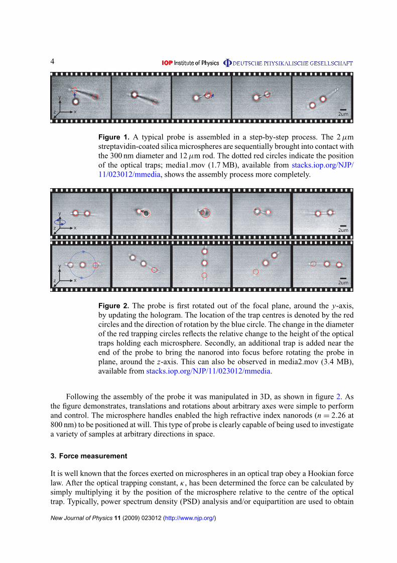
Figure 2. The probe is first rotated out of the focal plane, around the y-axis,by updating the hologram. The location of the trap centres is denoted by the redcircles and the direction of rotation by the blue circle. The change in the diameterof the red trapping circles reflects the relative change to the height of the opticaltraps holding each microsphere. Secondly, an additional trap is added near theend of the probe to bring the nanorod into focus before rotating the probe inplane, around the z-axis. This can also be observed in media2.mov (3.4 MB),available from stacks.iop.org/NJP/11/023012/mmedia.
Following the assembly of the probe it was manipulated in 3D, as shown in figure 2. Asthe figure demonstrates, translations and rotations about arbitrary axes were simple to performand control. The microsphere handles enabled the high refractive index nanorods (n = 2.26 at800 nm) to be positioned at will. This type of probe is clearly capable of being used to investigatea variety of samples at arbitrary directions in space.
3. Force measurement
It is well known that the forces exerted on microspheres in an optical trap obey a Hookian forcelaw. After the optical trapping constant, κ , has been determined the force can be calculated bysimply multiplying it by the position of the microsphere relative to the centre of the opticaltrap. Typically, power spectrum density (PSD) analysis and/or equipartition are used to obtain
New Journal of Physics 11 (2009) 023012 (http://www.njp.org/)

5
optical trapping constants in both the x-(horizontal) and y-(vertical) directions [32]. As theshape of the probe adds complexity to the PSD calculations, only equipartition was used tocalibrate the trap; yielding trap constants of κ0 ≡ (κ0,x , κ0,y) = (4.72 × 10⁻⁵, 4.58 × 10⁻⁵) Nand κ1 = (4.77 × 10⁻⁵, 5.16 × 10⁻⁵) N. To verify the calibration Stokes drag was employed.The stage was translated at a constant velocity of 12.75 µm s−1, perpendicular to the long axisof the probe, while maintaining a constant hologram image to avoid artefacts caused by thediscrete positioning of the optical traps between hologram updates [33]. Theory predicts that atranslation of this velocity should result in force of ≈2.12 × 10⁻¹² N per sphere, which agreeswithin 10% with the measured average of 2.25 × 10⁻¹² N. Between translations, when onlythermal fluctuations will provide forces, the difference in consecutive forces was found to be5.0 × 10−14 N, or 50 fN, 20 times more sensitive than most AFM techniques.
To demonstrate the ability to apply forces to materials the probe was brought into contactwith a silicon shard, which had adsorbed to the surface of the sample chamber, numeroustimes. Continuous data and video were recorded during this process, media3.mov (availablefrom stacks.iop.org/NJP/11/023012/mmedia) shows the process in its entirety. The stage wastranslated at 12.75 µm s−1 and each collision moved the probe to different distances relative tothe shard, resulting in different applied forces. After the probe makes contact with the samplein the first collision it slightly rotates about its central point, between the trapped microspheres.This is seen as the difference in the signs of y0 and y1 traces in the force plots. In the secondcollision event the silicon shard ‘catches’ one of the nodules on the end of the nanorod andimpedes the retraction of the probe. In collision 3, the probe tip initially slides on the sample,initially rotating the probe as in collision 1, but the total distance the probe is moved is increasedfurther and the entire probe then moves in the y- and z-planes. Collision 4 shows the effect offurther decreasing the distance between the optical traps and the silicon shard. In this case, thetip eventually slides around the shard and a minor catch is seen during the retraction. Collision 5shows a smaller displacement of the stage and hence a lower applied force. There is virtually noy-movement in this case and all force is applied purely opposing the motion along the length ofthe rod. Collision 6 shows the effect of vastly reducing the optical trap–shard distance. The forceexerted on the probe increases to such an extent that the probe almost completely defocuses intrap 0 before the probe slides around the shard. The small nodule observed approximately 1 µmfrom the tip catches on the shard during the retraction of the probe. In this case the probe waspulled from the optical trap and particle p0 ended up residing in trap 1, allowing the entire probeto rotate and be freed from the shard.
To emphasise the video more clearly, figure 3 displays three images from the 4th collisionand a zoomed in section of the force profile. Similar detailed analyses could have beenperformed on any of the other probing events. The green dashed lines are used to illustratethe time and corresponding forces of each frame. The timelines on the charts have not beenmodified, maintaining the time relationship with the movie. In the first frame the probe had justmade contact with the shard, and consequently no forces are observed. As time progresses anincreasing amount of force is applied. The difference in the magnitude of the forces measuredby x0 and x1 is a result of the changes in the focal plane of the microspheres (not measured).The relative intensity of x0 and x1 could be used to indicate the amount of z-defocusing and theconsequent height of both microspheres. Between t = 8.82 s and 8.87 s the different sign of Fy,0
and Fy,1 indicates that the probe twists about a point between the two microspheres within thetrapping plane. The second frame shows the displacement of each microsphere with respect tothe optical trap centres, and defocusing of the entire probe can be observed. The force profile
New Journal of Physics 11 (2009) 023012 (http://www.njp.org/)

6
Figure 3. Three frames have been extracted from media3.mov (3.2 MB) andare shown with an expanded view of the applied forces. The green dashed linesindicate the time each frame is sampled. p0 and p1 refer to the locations ofoptical trap 0 and 1 (red circles), and also show the location of the centres of themicrospheres attached to the nanorod. The stage was translated at 12.75 µm s−1,until the probe collides with a silicon shard adhered to the surface (frame 1). Therelative defocussing and torques can be calculated from the force profiles.
demonstrates that the entire probe shifts in the +y-direction at t = 8.92 s, enabling the probe toslip from its initial location at t = 8.96 s and slide around the point of the shard. A torque eventis clearly present by inspection of the movie and the y force profiles. Frame 3 of figure 3 showsthe tip protruding past the top of the shard. Forces Fx,0, Fx,1 and Fy,0 return to near zero force,and only the forces rotating the probe are seen in Fy,1. At this point in time the user reversed thedirection of the probe, resulting in the observed plateau and reduction of torque.
4. Conclusions
SPM-like probes have been assembled from steptavidin-coated silica microspheres and biotin-coated CdS rods. In the future the tips of such rods could be functionalized. The range of forcesthat these probes can exert on an external structure have been demonstrated to range from 50 fNto in excess of 60 pN. While the extent of the residual Brownian motion means that the techniqueis unlikely to result in the same levels of positional control capable with current SPM systems,this proof of principle study demonstrates potential uses of optically trapped probes within
New Journal of Physics 11 (2009) 023012 (http://www.njp.org/)

7
liquid media, compatible with biological systems. In particular, this type of probe could beused to investigate a living cell in true environmental conditions, something that will challengetraditional SPMs.
Acknowledgment
This project is funded by a Basic Technology Grant through the Research Councils of the UnitedKingdom.
References
[1] Baker A A, Helbert W, Sugiyama J and Miles M J 1997 High-resolution atomic force microscopy of nativevalonia cellulose I microcrystals J. Struct. Biol. 119 129–38
[2] Grandbois M, Dettmann W, Benoit M and Gaub H E 2000 Affinity imaging of red blood cells using an atomicforce microscope J. Histochem. Cytochem. 48 719–24
[3] Chtcheglova L A, Waschke J, Wildling L, Drenckhahn D and Hinterdorfer P 2007 Nano-scale dynamicrecognition imaging on vascular endothelial cells Biophys. J. 93 L11–3
[4] Florin E L, Moy V T and Gaub H E 1994 Adhesion forces between individual ligand-receptor pairs Science264 415–7
[5] Humphris A D L, Tamayo J and Miles M J 2000 Active quality factor control in liquids for force spectroscopyLangmuir 16 7891–4
[6] Haupt B J, Senden T J and Sevick E M 2002 AFM Evidence of Rayleigh instability in single polymer chainsLangmuir 18 2174–82
[7] Dai G, Wolff H, Pohlenz F, Danzebrink H-U and Wilkening G 2006 Atomic force probe for sidewall scanningof nano- and microstructures Appl. Phys. Lett. 88 171908
[8] Bustamante C, Smith S B, Liphardt J and Smith D 2000 Single-molecule studies of DNA mechanics Curr.Opin. Struct. Biol. 10 279–85
[9] Ashkin A and Dziedzic J M 1989 Internal cell manipulation using infrared laser traps Proc. Natl Acad. Sci.USA 86 7914–8
[10] Yu T, Cheong F-C and Sow C-H 2004 The manipulation and assembly of CuO nanorods with line opticaltweezers Nanotechnology 15 1732–6
[11] Benito D C, Carberry D M, Simpson S H, Gibson G M, Padgett M J, Rarity J G, Miles M J and Hanna S 2008Constructing 3D crystal templates for photonic band gap materials using holographic optical tweezers Opt.Express 16 13005–15
[12] Jordan P, Cooper J, McNay G, Docherty F, Graham D, Smith W, Sinclair G and Padgett M J 2005 Surface-enhanced resonance Raman scattering in optical tweezers using co-axial second harmonic generation Opt.Express 13 4148
[13] Wang Y, Botvinick E L, Zhao Y, Berns M W, Usami S, Tsien R Y and Chien S 2005 Visualizing themechanical activation of src Nature 434 1040–5
[14] Reicherter M, Haist T, Wagemann E U and Tiziani H J 1999 Optical particle trapping with computer-generatedholograms written on a liquid-crystal display Opt. Lett. 24 608–10
[15] Curtis J E, Koss B A and Grier D G 2002 Dynamic holographic optical tweezers Opt. Commun. 207 169–75[16] Simpson S H and Hanna S 2006 Numerical calculation of interparticle forces arising in association with
holographic assembly J. Opt. Soc. Am. A 23 1419–31[17] Sinclair G, Jordan P, Courtial J, Padgett M J, Cooper J and Laczik Z 2004 Assembly of 3-dimensional
structures using programmable holographic optical tweezers Opt. Express 12 5475–80[18] Friese M E J, Truscott A G, Rubinsztein-Dunlop H and Heckenberg N R 1999 Three-dimensional imaging
with optical tweezers Appl. Opt. 38 6597–6603
New Journal of Physics 11 (2009) 023012 (http://www.njp.org/)

8
[19] Ghislain L P and Webb W W 1993 Scanning-force microscope based on an optical trap Opt. Lett. 18 1678[20] Rodrigo P J, Gammelgaard L, Bøggild P, Perch-Nielsen I and Glückstad J 2005 Actuation of microfabricated
tools using multiple GPC-based counterpropagating-beam traps Opt. Express 13 6899–904[21] Pauzauskie P J, Radenovic A, Trepagnier E, Shroff H, Yang P and Liphardt J 2006 Optical trapping and
integration of semiconductor nanowire assemblies in water Nat. Mater. 5 97–101[22] van der Horst A, Campbell A I, van Vugt L K, Vanmaekelbergh D A, Dogterom M and van Blaaderen A
2007 Manipulating metal-oxide nanowires using counter-propagating optical line tweezers Opt. Express15 11629–39
[23] Dai H, Hafner J H, Rinzler A G, Colbert D T and Smalley R E 1996 Nanotubes as nanoprobes in scanningprobe microscopy Nature 384 147–50
[24] Seo J W, Couteau E, Umek P, Hernadi K, Marcoux P, Lukic B, Miko Cs, Milas M, Gaal R and Forro L 2003Synthesis and manipulation of carbon nanotubes New J. Phys. 5 120
[25] Gibson G, Carberry D M, Whyte G, Leach J, Courtial J, Jackson J C, Robert D J, Miles M J and Padgett M2008 Holographic assembly workstation for optical manipulation J. Opt. A: Pure Appl. Opt. 10 044009
[26] Saunter C D, Love G D, Johns M and Holmes J 2005 FPGA technology for high speed, low cost adaptiveoptics—art. no. 61081g 5th International Workshop on Adaptive Optics for Industry and Medicine, Beijing,Peoples Republic of China ed W H Jiang p 429
[27] Di Leonardo R, Keen S, Leach J, Saunter C D, Love G D, Ruocco G and Padgett M J 2007 Eigenmodes of ahydrodynamically coupled micron-size multiple-particle ring Phys. Rev. E 76 061402
[28] Ma R M, Wei X L, Dai L, Huo H B and Qin G G 2007 Synthesis of CdS nanowire networks and their opticaland electrical properties Nanotechnology 18 205605
[29] Ikin L, Carberry D M, Grieve J A, Gibson G M, Padgett M J and Miles M J 2008 Construction andmanipulation of structures using optical tweezers SPIE Optics and Photonics (San Diego, CA: SPIE)
[30] Benito D C, Simpson S H and Hanna S 2008 FDTD simulations of forces on particles during holographicassembly Opt. Express 16 2942–57
[31] Agarwal R, Ladavac K, Roichman Y, Yu G, Lieber C M and Grier D G 2005 Manipulation and assembly ofnanowires with holographic optical traps Opt. Express 13 8906–12
[32] Gibson G M, Leach J, Keen S, Wright A J and Padgett M J 2008 Measuring the accuracy of particle positionand force in optical tweezers using high-speed video microscopy Opt. Express 16 14561–70
[33] Eriksson E, Keen S, Leach J, Goksör M and Padgett M J 2007 The effect of external forces on discrete motionwithin holographic optical tweezers Opt. Express 15 18268–74
New Journal of Physics 11 (2009) 023012 (http://www.njp.org/)