IKI10201 05c-Decoders, Selectors, etc. Bobby Nazief Semester-I 2005 - 2006 The materials on these...
37
IKI10201 05c-Decoders, Selectors, etc. Bobby Nazief Semester-I 2005 - 2006 The materials on these slides are adopted from: •CS231’s Lecture Notes at UIUC, which is derived from Howard Huang’s work and developed by Jeff Carlyle; •Prof. Daniel Gajski’s transparency for Principles of Digital Design.
-
Upload
paulina-craig -
Category
Documents
-
view
218 -
download
0
Transcript of IKI10201 05c-Decoders, Selectors, etc. Bobby Nazief Semester-I 2005 - 2006 The materials on these...

IKI10201 05c-Decoders, Selectors, etc.
Bobby NaziefSemester-I 2005 -
2006
The materials on these slides are adopted from:
•CS231’s Lecture Notes at UIUC, which is derived from Howard Huang’s work and developed by Jeff Carlyle;
•Prof. Daniel Gajski’s transparency for Principles of Digital Design.
2
Decoders
• Next, we’ll look at some commonly used circuits: decoders and selectors (multiplexers or MUXes).
– They can be used to implement arbitrary functions.
– We are introduced to abstraction and modularity as hardware design principles.

3
What is a decoder?
• In older days, the (good) printers used be like typewriters:
– To print “A”, a wheel turned, brought the “A” key up, which then was struck on the paper.
• Letters are encoded as 8 bit (ASCII) codes inside the computer.
– When the particular combination of bits that encodes “A” is detected, we want to activate the output line corresponding to A
– (Not actually how the wheels worked)
• How to do this “detection” : decoder
• General idea: given a k bit input,
– Detect which of the 2^k combinations is represented
– Produce 2^k outputs, only one of which is “1”.

4
What a decoder does
• A n-to-2n decoder takes an n-bit input and produces 2n outputs. The n inputs represent a binary number that determines which of the 2n outputs is uniquely true.
• A 2-to-4 decoder operates according to the following truth table.
– The 2-bit input is called S1S0, and the four outputs are Q0-Q3.
– If the input is the binary number i, then output Qi is uniquely true.
• For instance, if the input S1 S0 = 10 (decimal 2), then output Q2 is true, and Q0, Q1, Q3 are all false.
• This circuit “decodes” a binary number into a “one-of-four” code.
S1 S0 Q0 Q1 Q2 Q3
0 0 1 0 0 00 1 0 1 0 01 0 0 0 1 01 1 0 0 0 1

5
How can you build a 2-to-4 decoder?
• Follow the design procedures from last time! We have a truth table, so we can write equations for each of the four outputs (Q0-Q3), based on the two inputs (S0-S1).
• In this case there’s not much to be simplified. Here are the equations:
S1 S0 Q0 Q1 Q2 Q3
0 0 1 0 0 00 1 0 1 0 01 0 0 0 1 01 1 0 0 0 1
Q0 = S1’ S0’Q1 = S1’ S0Q2 = S1 S0’Q3 = S1 S0

6
A picture of a 2-to-4 decoder
S1 S0 Q0 Q1 Q2 Q3
0 0 1 0 0 00 1 0 1 0 01 0 0 0 1 01 1 0 0 0 1

7
Enable inputs
• Many devices have an additional enable input, which is used to “activate” or “deactivate” the device.
• For a decoder,
– EN=1 activates the decoder, so it behaves as specified earlier. Exactly one of the outputs will be 1.
– EN=0 “deactivates” the decoder. By convention, that means all of the decoder’s outputs are 0.
• We can include this additional input in the decoder’s truth table:
EN S1 S0 Q0 Q1 Q2 Q3
0 x x 0 0 0 0
1 0 0 1 0 0 01 0 1 0 1 0 01 1 0 0 0 1 01 1 1 0 0 0 1

8
• Decoders are common enough that we want to encapsulate them and treat them as an individual entity.
• Block diagrams for 2-to-4 decoders are shown here. The names of the inputs and outputs, not their order, is what matters.
• A decoder block provides abstraction:
– You can use the decoder as long as you know its truth table or equations, without knowing exactly what’s inside.
– It makes diagrams simpler by hiding the internal circuitry.
– It simplifies hardware reuse. You don’t have to keep rebuilding the decoder from scratch every time you need it.
• These blocks are like functions in programming!
Blocks and abstraction
Q0 = S1’ S0’Q1 = S1’ S0Q2 = S1 S0’Q3 = S1 S0

9
A 3-to-8 decoder
• Larger decoders are similar. Here is a 3-to-8 decoder.
– The block symbol is on the right.
– A truth table (without EN) is below.
– Output equations are at the bottom right.
• Again, only one output is true for any input combination.
S2 S1 S0 Q0 Q1 Q2 Q3 Q4 Q5 Q6 Q7
0 0 0 1 0 0 0 0 0 0 00 0 1 0 1 0 0 0 0 0 00 1 0 0 0 1 0 0 0 0 00 1 1 0 0 0 1 0 0 0 01 0 0 0 0 0 0 1 0 0 01 0 1 0 0 0 0 0 1 0 01 1 0 0 0 0 0 0 0 1 01 1 1 0 0 0 0 0 0 0 1
Q0 = S2’ S1’ S0’Q1 = S2’ S1’ S0Q2 = S2’ S1 S0’Q3 = S2’ S1 S0Q4 = S2 S1’ S0’Q5 = S2 S1’ S0Q6 = S2 S1 S0’Q7 = S2 S1 S0
10
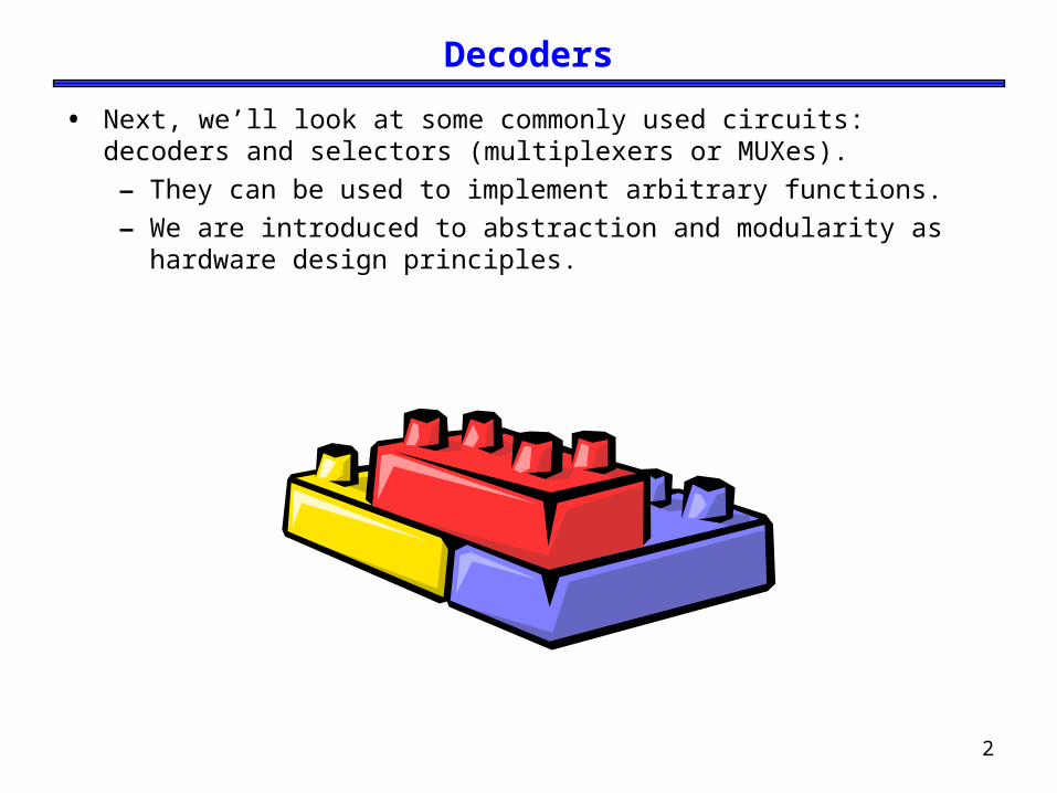
Building a 3-to-8 decoder
• You could build a 3-to-8 decoder directly from the truth table and equations below, just like how we built the 2-to-4 decoder.
• Another way to design a decoder is to break it into smaller pieces.
• Notice some patterns in the table below:
– When S2 = 0, outputs Q0-Q3 are generated as in a 2-to-4 decoder.
– When S2 = 1, outputs Q4-Q7 are generated as in a 2-to-4 decoder.
S2 S1 S0 Q0 Q1 Q2 Q3 Q4 Q5 Q6 Q7
0 0 0 1 0 0 0 0 0 0 00 0 1 0 1 0 0 0 0 0 00 1 0 0 0 1 0 0 0 0 00 1 1 0 0 0 1 0 0 0 0
1 0 0 0 0 0 0 1 0 0 01 0 1 0 0 0 0 0 1 0 01 1 0 0 0 0 0 0 0 1 01 1 1 0 0 0 0 0 0 0 1
Q0 = S2’ S1’ S0’ = m0
Q1 = S2’ S1’ S0 = m1
Q2 = S2’ S1 S0’ = m2
Q3 = S2’ S1 S0 = m3
Q4 = S2 S1’ S0’ = m4
Q5 = S2 S1’ S0 = m5
Q6 = S2 S1 S0’ = m6
Q7 = S2 S1 S0 = m7

11
Decoder expansion
• You can use enable inputs to string decoders together. Here’s a 3-to-8 decoder constructed from two 2-to-4 decoders:
S2 S1 S0 Q0 Q1 Q2 Q3 Q4 Q5 Q6 Q7
0 0 0 1 0 0 0 0 0 0 00 0 1 0 1 0 0 0 0 0 00 1 0 0 0 1 0 0 0 0 00 1 1 0 0 0 1 0 0 0 0
1 0 0 0 0 0 0 1 0 0 01 0 1 0 0 0 0 0 1 0 01 1 0 0 0 0 0 0 0 1 01 1 1 0 0 0 0 0 0 0 1

12
So what good is a decoder?
• Do the truth table and equations look familiar?
• Decoders are sometimes called minterm generators.
– For each of the input combinations, exactly one output is true.
– Each output equation contains all of the input variables.
– These properties hold for all sizes of decoders.
• This means that you can implement arbitrary functions with decoders. If you have a sum of minterms equation for a function, you can easily use a decoder (a minterm generator) to implement that function.
S1 S0 Q0 Q1 Q2 Q3
0 0 1 0 0 00 1 0 1 0 01 0 0 0 1 01 1 0 0 0 1
Q0 = S1’ S0’Q1 = S1’ S0Q2 = S1 S0’Q3 = S1 S0
13
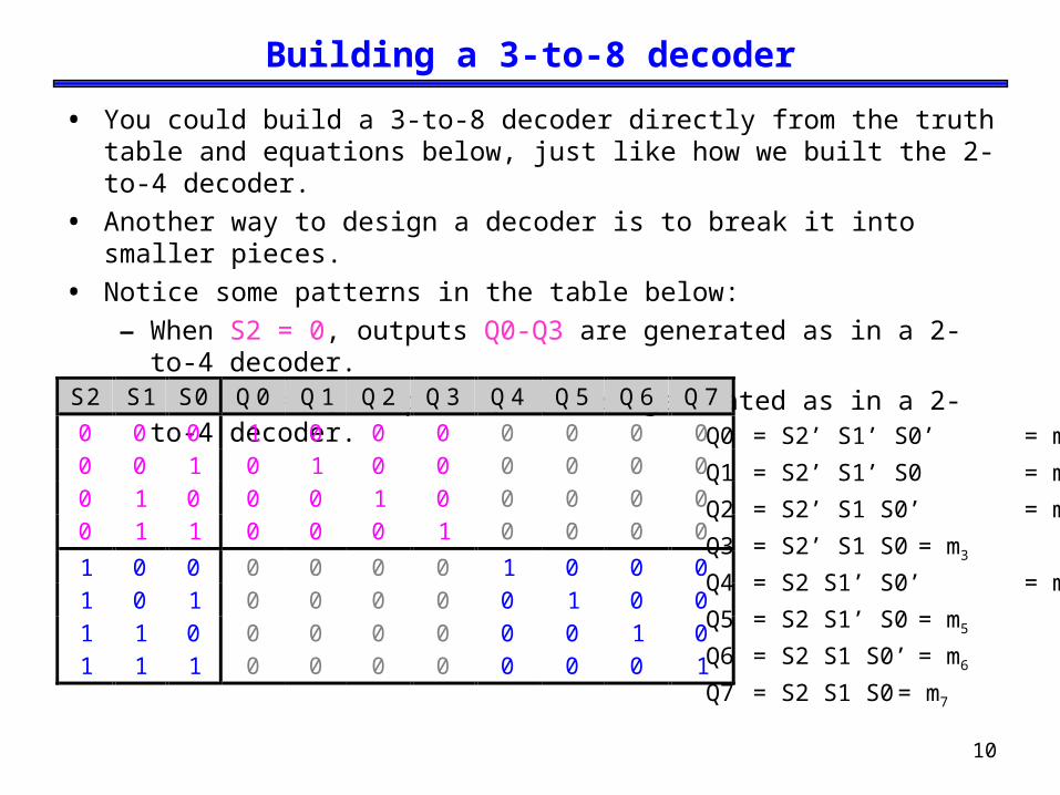
Design example: addition
• Let’s make a circuit that adds three 1-bit inputs X, Y and Z.
• We will need two bits to represent the total; let’s call them C and S, for “carry” and “sum.” Note that C and S are two separate functions of the same inputs X, Y and Z.
• Here are a truth table and sum-of-minterms equations for C and S.
X Y Z C S
0 0 0 0 00 0 1 0 10 1 0 0 10 1 1 1 01 0 0 0 11 0 1 1 01 1 0 1 01 1 1 1 1 1 + 1 + 1 = 11
0 + 1 + 1 = 10 C(X,Y,Z) = m(3,5,6,7)S(X,Y,Z) = m(1,2,4,7)

14
Decoder-based adder
C(X,Y,Z) = m(3,5,6,7)S(X,Y,Z) = m(1,2,4,7)
• Here is how a 3-to-8 decoder implements C and S as sums of minterms

15
Selectors/Multiplexers
• Now we’ll study multiplexers, which are just as commonly used as the decoders we presented last time. Again,
– Multiplexers can implement arbitrary functions.
– We will put these circuits to use in later weeks, as building blocks for more complex designs.

16
Multiplexers
• A 2n-to-1 multiplexer sends one of 2n input lines to a single output line.
– A multiplexer has two sets of inputs:
• 2n data input lines
• n select lines, to pick one of the 2n data inputs
– The mux output is a single bit, which is one of the 2n data inputs.
• The simplest example is a 2-to-1 mux:
• The select bit S controls which of the data bits D0-D1 is chosen:
– If S=0, then D0 is the output (Q=D0).
– If S=1, then D1 is the output (Q=D1).
Q = S’ D0 + S D1

17
More truth table abbreviations
• Here is a full truth table for this 2-to-1 mux, based on the equation:
• Here is another kind of abbreviated truth table.
– Input variables appear in the output column.
– This table implies that when S=0, the output Q=D0, and when S=1 the output Q=D1.
– This is a pretty close match to the equation.
S D1 D0 Q
0 0 0 00 0 1 10 1 0 00 1 1 1
1 0 0 01 0 1 01 1 0 11 1 1 1
Q = S’ D0 + S D1
S Q
0 D01 D1

18
A 4-to-1 multiplexer
• Here is a block diagram and abbreviated truth table for a 4-to-1 mux.
EN’ S1 S0 Q
0 0 0 D00 0 1 D10 1 0 D20 1 1 D3
1 x x 1
Q = S1’ S0’ D0 + S1’ S0 D1 + S1 S0’ D2 + S1 S0 D3

19
Implementing functions with multiplexers
• Muxes can be used to implement arbitrary functions.
• One way to implement a function of n variables is to use an n-to-1 mux:
– For each minterm mi of the function, connect 1 to mux data input Di. Each data input corresponds to one row of the truth table.
– Connect the function’s input variables to the mux select inputs. These are used to indicate a particular input combination.
• For example, let’s look at f(x,y,z) = m(1,2,6,7).x y z f
0 0 0 00 0 1 10 1 0 10 1 1 01 0 0 01 0 1 01 1 0 11 1 1 1
20
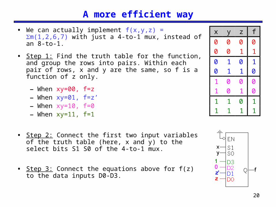
A more efficient way
• We can actually implement f(x,y,z) = m(1,2,6,7) with just a 4-to-1 mux, instead of an 8-to-1.
• Step 1: Find the truth table for the function, and group the rows into pairs. Within each pair of rows, x and y are the same, so f is a function of z only.
– When xy=00, f=z– When xy=01, f=z’– When xy=10, f=0– When xy=11, f=1
• Step 2: Connect the first two input variables of the truth table (here, x and y) to the select bits S1 S0 of the 4-to-1 mux.
• Step 3: Connect the equations above for f(z) to the data inputs D0-D3.
x y z f
0 0 0 00 0 1 1
0 1 0 10 1 1 0
1 0 0 01 0 1 0
1 1 0 11 1 1 1

21
Buses
• Bus drivers have three possible output values:0, 1, and Z (high impedance ~ disconnection)

22
Priority Encoders
• Encoder is opposite of Decoder, but with priority for MSB

23
Magnitude Comparators
• Comparator compares two integers A and B and sets:
– G = 1 when A > B
– L = 1 when A < B
– G = L = 0 when A = B

24
Shifter & Rotators
• Shifter shifts input bits to the left/right
– Shift left: X3X2X1X0 X2X1X00
– Shift right: X3X2X1X0 0X3X2X1
• Rotator is a Shifter with additional shift from one end to the other:
– Rotate left: X3X2X1X0 X2X1X0X3
– Rotate right: X3X2X1X0 X0X3X2X1

25
Read Only Memory (ROM)
• A read-only memory, or ROM, is a special kind of memory whose contents cannot be easily modified.
– Data is stored onto a ROM chip using special hardware tools.
• ROMs are useful for holding data that never changes.
– Arithmetic circuits might use tables to speed up computations of logarithms or divisions.
– Many computers use a ROM to store important programs that should not be modified, such as the system BIOS.
– PDAs, game machines, cell phones, vending machines and other electronic devices may also contain non-modifiable programs.
2k x n ROM
ADRS OUTCS
k n

26
Memories and functions
• ROMs are actually combinational devices, not sequential ones!
– You can’t store arbitrary data into a ROM, so the same address will always contain the same data.
– You can think of a ROM as a combinational circuit that takes an address as input, and produces some data as the output.
• A ROM table is basically just a truth table.
– The table shows what data is stored at each ROM address.
– You can generate that data combinationally, using the address as the input.
• Data = F(A0,A1,A2)
AddressA2A1A0
DataV2V1V0
000 000001 100010 110011 100
100 101101 000110 011111 011

27
Implementing functions with decoders
• We can already convert truth tables to circuits easily, with decoders.
• For example, you can think of this old circuit as a memory that “stores” the sum and carry outputs from the truth table on the right.
X Y Z C S
0 0 0 0 00 0 1 0 10 1 0 0 10 1 1 1 01 0 0 0 11 0 1 1 01 1 0 1 01 1 1 1 1

28
Implementing functions with ROM
• ROMs are based on this decoder implementation of functions.
– A blank ROM just provides a decoder and several OR gates.
– The connections between the decoder and the OR gates are “programmable,” so different functions can be implemented.
• To program a ROM, you just make the desired connections between the decoder outputs and the OR gate inputs.

29
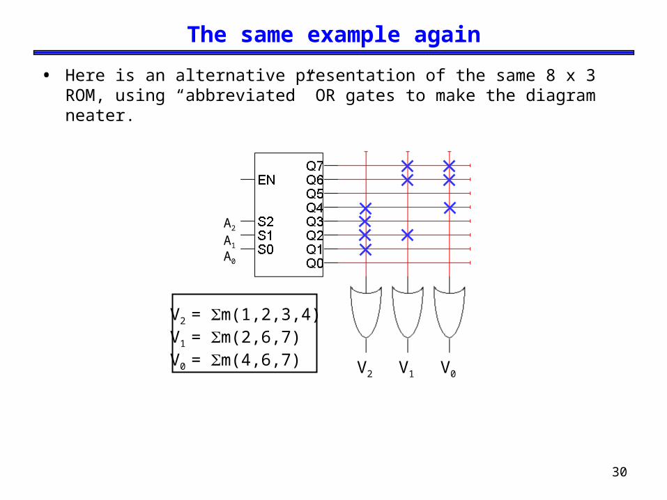
Implementing functions with ROM (cont.)
• Here are three functions, V2V1V0, implemented with an 8 x 3 ROM.
• Blue crosses (X) indicate connections between decoder outputs and OR gates. Otherwise there is no connection.
V2 = m(1,2,3,4)
A2
A1
A0
V1 = m(2,6,7)
V0 = m(4,6,7)
30
V2 V1 V0
A2
A1
A0
The same example again
• Here is an alternative presentation of the same 8 x 3 ROM, using “abbreviated” OR gates to make the diagram neater.
V2 = m(1,2,3,4)V1 = m(2,6,7)V0 = m(4,6,7)

31
Why is this a “memory”?
• This combinational circuit can be considered a read-only memory.
– It stores eight words of data, each consisting of three bits.
– The decoder inputs form an address, which refers to one of the eight available words.
– So every input combination corresponds to an address, which is “read” to produce a 3-bit data output.
V2 V1 V0
A2
A1
A0
AddressA2A1A0
DataV2V1V0
000 000001 100010 110011 100
100 101101 000110 011111 011

32
ROMs vs. RAMs
• There are some important differences between ROM and RAM.
– ROMs are “non-volatile”—data is preserved even without power. On the other hand, RAM contents disappear once power is lost.
– ROMs require special (and slower) techniques for writing, so they’re considered to be “read-only” devices.
• Some newer types of ROMs do allow for easier writing, although the speeds still don’t compare with regular RAMs.
– MP3 players, digital cameras and other toys use CompactFlash, Secure Digital, or MemoryStick cards for non-volatile storage.
– Many devices allow you to upgrade programs stored in “flash ROM.”
33
Programmable logic arrays (PLAs)
• A ROM is potentially inefficient because it uses a decoder, which generates all possible minterms. No circuit minimization is done.
• Using a ROM to implement an n-input function requires:
– An n-to-2n decoder, with n inverters and 2n n-input AND gates.
– An OR gate with up to 2n inputs.
– The number of gates roughly doubles for each additional ROM input.
• A programmable logic array, or PLA, makes the decoder part of the ROM “programmable” too. Instead of generating all minterms, you can choose which products (not necessarily minterms) to generate.

34
A blank 3 x 4 x 3 PLA
• This is a 3 x 4 x 3 PLA (3 inputs, up to 4 product terms, and 3 outputs), ready to be programmed.
• The left part of the diagram replaces the decoder used in a ROM.
• Connections can be made in the “AND array” to produce four arbitrary products, instead of 8 minterms as with a ROM.
• Those products can then be summed together in the “OR array.”
Inputs
Outputs
AND array
OR array
35
Example: PLA minimization
• For a PLA, we should minimize the number of product terms for all functions together (K-Map minimization individual function).
• We should express V2, V1 and V0 with no more than four total products.
Y
0 0 0 0
X 1 0 1 1
Z
Y
0 1 1 1
X 1 0 0 0
Z
Y
0 0 0 1
X 0 0 1 1
Z
V2 = xy’z’ + x’z + x’yz’ V1 = x’yz’ + xy V0 = xy’z’ + xy
V2 = m(1,2,3,4)V1 = m(2,6,7)V0 = m(4,6,7)

36
Example: PLA implementation
• So we can implement these three functions using a 3 x 4 x 3 PLA:
V2 V1 V0
xy’z’
xy
x’z
x’yz’
V2 = m(1,2,3,4) = xy’z’ + x’z + x’yz’V1 = m(2,6,7) = x’yz’ + xyV0 = m(4,6,7) = xy’z’ + xy
A2 A1 A0

37
PLA evaluation
• A k x m x n PLA can implement up to n functions of k inputs, each of which must be expressible with no more than m product terms.
• Unlike ROMs, PLAs allow you to choose which products are generated.
– This can significantly reduce the fan-in (number of inputs) of gates, as well as the total number of gates.
– However, a PLA is less general than a ROM. Not all functions may be expressible with the limited number of AND gates in a given PLA.
• In terms of memory, a k x m x n PLA has k address lines, and each of the 2k addresses references an n-bit data value.
• But again, not all possible data values can be stored.