III. Introduction to Bipolar-Junction...
30
III. Introduction to Bipolar-Junction Transistors 3.1 BJT iv characteristics A bipolar junction transistor is formed by joining three sections of semiconductors with alternative different dopings. The middle section (base) is narrow and one of the other two regions (emitter) is heavily doped. The other region is called the collector. B C E n + n BE junction BC junction p Two variants of BJT are possible: NPN (base is made of p-type material) and PNP (base is made of n-type material). Let’s first consider a NPN transistor. A simplified physical structure of a NON transistor is shown on the right. i E i C B i v BC v BE v CE + + + - - - A BJT has three terminals. Six parameters; i C , i B , i E , v CE , v BE , and v BC ; define the state of the transistor. However, because a BJT has three terminals, KVL and KCL should hold for these terminals: i E = i C + i B v BC = v BE − v CE Thus, only four of these 6 parameters are independent. Two relationships among these four parameters (i B ,v BE ,i C and v CE ) represent the “iv” characteristics of the BJT. A BJT looks like 2 diodes placed back to back if we apply a voltage to only two of the three terminals, letting the third terminal float. We can use this feature to check if a transistor is working: use a multi-meter to ensure that both diodes are in working condition. (One should also check the resistance between C & E terminals and read a vary high resistance as one may have a burn through the base connecting collector and emitter.) v BE B E C n + + - n BE junction BC junction p electrons holes When the BE junction is forward biased, electrons from the emitter diffuse into the base and holes from the base into the emitter setting up the BE diode diffusion current. Because the emitter is heavily doped, a large number of electrons enter the base. If the base is thin enough, there would be a substantial number of electrons in the vicinity of the BC junction. v BE v CB B E C n + + - + - electrons n p holes If a “negative” voltage is applied to the BC junction, the elec- trons from the emitter which had diffused to the vicinity of the BC junction are swept into the collector (a drift current). As a result, a substantial current flows between emitter and collector terminals. Note that the BC junction is reversed biased in this case (but the BC junction does not “act” as a diode). ECE65 Lecture Notes (F. Najmabadi), Winter 2011 3-1
-
Upload
truongkiet -
Category
Documents
-
view
237 -
download
2
Transcript of III. Introduction to Bipolar-Junction...

III. Introduction to Bipolar-Junction Transistors
3.1 BJT iv characteristics
A bipolar junction transistor is formed by joining three sections of semiconductors with
alternative different dopings. The middle section (base) is narrow and one of the other two
regions (emitter) is heavily doped. The other region is called the collector.
B
CEn+ n
BE junction BC junction
p
Two variants of BJT are possible: NPN (base is made of p-type
material) and PNP (base is made of n-type material). Let’s first
consider a NPN transistor. A simplified physical structure of a
NON transistor is shown on the right.
iE
iC
BivBC
vBE
vCE++
+
−
−
−
A BJT has three terminals. Six parameters; iC , iB, iE, vCE, vBE,
and vBC ; define the state of the transistor. However, because a BJT
has three terminals, KVL and KCL should hold for these terminals:
iE = iC + iB vBC = vBE − vCE
Thus, only four of these 6 parameters are independent. Two relationships among these four
parameters (iB, vBE, iC and vCE) represent the “iv” characteristics of the BJT.
A BJT looks like 2 diodes placed back to back if we apply a voltage to only two of the three
terminals, letting the third terminal float. We can use this feature to check if a transistor
is working: use a multi-meter to ensure that both diodes are in working condition. (One
should also check the resistance between C & E terminals and read a vary high resistance
as one may have a burn through the base connecting collector and emitter.)
vBEB
E Cn+
+−
n
BE junction BC junction
p
electrons
holes
When the BE junction is forward biased, electrons from the
emitter diffuse into the base and holes from the base into the
emitter setting up the BE diode diffusion current. Because the
emitter is heavily doped, a large number of electrons enter the
base. If the base is thin enough, there would be a substantial
number of electrons in the vicinity of the BC junction.
vBE vCBB
E Cn+
+− +−
electrons
np
holes
If a “negative” voltage is applied to the BC junction, the elec-
trons from the emitter which had diffused to the vicinity of the
BC junction are swept into the collector (a drift current). As a
result, a substantial current flows between emitter and collector
terminals. Note that the BC junction is reversed biased in this
case (but the BC junction does not “act” as a diode).
ECE65 Lecture Notes (F. Najmabadi), Winter 2011 3-1

This mode of operation is called the active mode: the BE junction is forward biased while
the BC junction is reversed biased:
vBE = VD0 & vBC < 0 → vCE = vCB + vBE > VD0
Since the BE junction acts as a diode, the number of electrons which diffused into base and
are near the BC junction scales as exp(vBE/VT ) (for an emission coefficient, n = 1). As all
these electrons will be swept into the collector, regardless of vBC (or vCE = vBE − vBC), the
collector current, iC should not depend on vCE. Furthermore,
iC = IS evBE/VT
The base current, iB, also scales as exp(vBE/VT ). However, because emitter is heavily doped
and base is thin, only a very small fraction of electrons that diffused into base combine with
holes – majority of emitter-originated electrons are swept into the collector. As such, the
ratio of iC/iB = β is large and relatively constant (but changes with temperature, etc.).
Parameter β is called the BJT common-emitter current gain (or current gain for short):
iB =ISβ
evBE/VT
As can be seen, operation of a BJT requires the presence of emitter-generated electrons near
the BC junction (thus, the BE junction should be forward biased). A BJT is called to be
in “cut-off” if the BE junction is NOT forward biased. In this case, iB = 0 and iC = 0
regardless of any voltage applied to the BC junction.
Now, let’s consider the case of the BC junction being forward biased (with BE junction still
forward biased), i.e., vCE = vBE − vBC < VD0. This is called the saturation mode.
As the BC junction is forward biased, a diffusion current is set up between the collector
and base regions (which is in the opposite direction to iB and iC). When vBC is small
(vBC < 0.3V , or vCE > 0.4V for Si), the diffusion current from the BC junction is negligible
and iC remains close to its value for the active mode. This region is usually called the “soft
saturation region.” Some text books include this region as part of the active mode, i.e., say
BJT is in active if vCE > 0.4 V (instead of vCE ≥ VD0 = 0.7 V).
When vBC becomes large enough (vCE ≈ 0.1 − 0.3 V for Si) a substantial diffusion current
flows from the collector to the base, thereby reducing iC below its active-mode level, i.e.,
iC < βiB. This is called the “deep saturation” region.
For vCE close to zero (vCE < 0.1 V for Si), the collector current rapidly goes to zero. This
region is referred to as the “near cut-off” region.
ECE65 Lecture Notes (F. Najmabadi), Winter 2011 3-2

BJT iv characteristics above is typically
shown as plot of iB vs vBE (similar to a
diode iv curve) and a “contour” plot of iCvs vCE with each contour lines representing
a value of iB. Note that iC = g(vCE, iB) is
actually a “surface” plot in the 3-D space
of iC , vCE, iB. The iCvCE plot shown is a
projection of this 3-D surface with the iBaxis pointing into the plane. An iCvCE plot
of a commercial BJT is shown on the right.
A transistor can be damaged if (1) a large positive voltage is applied between the collector and
emitter (breakdown region), or (2) product of iCvCE exceed the power handling capability
of the transistor, or (3) a large reverse voltage is applied between any two terminals.
Our rather simple description of the oper-
ation of a BJT in the active mode indi-
cated that for a given iB, iC = βiB and
is independent of vCE. However, as iCvCE
plot above shows, iC increases slightly with
vCE. The reason for this increase in iCis that as vCE is increased, the “effec-
tive” width of the base region is reduced
and more electrons can reach the collector.
This is called the “Early” effect.
In fact, if we extrapolate all characteristics lines of the active region, they would meet at
a negative voltage of vCE = −VA as is shown. The voltage VA is particular to each BJT
(depends on its manufacturing) and has a typical value of 50 to 100 V. It is called the “Early”
voltage. The Early effect can be accounted for by the following addition to the iC equation
(Note that iB equation does NOT change):
iC = ISevBE/VT
(
1 +vCE
VA
)
The above model, reproduced in the table below, is called a “large signal” model as it
applies to any size currents/voltages applied to the BJT (as opposed to a “small-signal”
model discussed later). While rather simple, it is quite sufficient for analysis. Note that the
explicit non-linear form is included only in the active mode equations (we will use this form
later). Furthermore, only “deep” saturation mode is included as for practical reasons, BJT
is only operated in deep saturation mode when it is used as a switch or a logic gate and soft
ECE65 Lecture Notes (F. Najmabadi), Winter 2011 3-3

saturation is usually avoided when BJT is used in the active mode (e.g., as an amplifier), in
order to reduce non-linear distortion.
PSpice uses the Ebers-Moll model which includes a better treatment of transistor operation
in the saturation mode. Furthermore, Ebers-Moll model provides a “smooth” transition
from active to saturation to cut-off modes which is necessary for numerical calculations.
Summary of BJT Large-Signal Models (NPN):
Large-signal model Linear Approximation
Cut-off:
BE reverse biased iB = 0 iB = 0, vBE < VD0
iC = 0 iC = 0
Active:
BE forward biased iB =ISβ
evBE/VT vBE = VD0, iB ≥ 0
CE reverse biased iC = IS evBE/VT
(
1 +vCE
VA
)
ic = βiB, vCE ≥ VD0
“Deep” Saturation:
BE forward biased vBE = VD0, iB ≥ 0
CE forward biased vCE = 0.1− 0.3 V, iC < βiB vCE = Vsat iC < βiB
For Si, VD0 = 0.7 V, Vsat = 0.2 V.
Similar to diodes, we need to use approximate linear models for BJT iv equations for hand
calculations and analysis. This can be easily achieved by using the diode constant voltage
model for the BE junction. Such a piecewise linear model is also listed in the table above.
Usually Early effect is ignored in such a linear approximation.
The BJT model above requires three parameters. Two (VD0 and Vsat) depend on the base
semiconductor, e.g., for Si, VD0 = 0.7 V, Vsat = 0.2 V. The third, β, depends on BJT
structure. Also, β changes substantially with temperature, depends on on iC , and can
vary in commercial BJTs of similar type due to manufacturing inaccuracies. Typically, the
manufacturer spec sheet specifies, an average value and a range for β of a BJT. The specified
βmin (minimum value of β) is an important parameter, i.e., all commercial BJTs of that type
have a β larger than βmin (although some BJTs can have a β which is lower than the average
value). This variation should be taken into account in designing BJT circuits. For example
for a BJT circuit operating in deep saturation, we should set iC/iB < βmin (instead of the
average β) to ensure that it works correctly for all commercial BJTs of that particular model.
ECE65 Lecture Notes (F. Najmabadi), Winter 2011 3-4

PNP transistor: A PNP transistor operates in a similar manner to a NPN BJT, expect
that holes (instead of electrons) from the emitter diffuse through the base, reach the vicinity
of the CB junction, and swept into the collector.
iE
iC
vCB
vEB
vEC
Bi
++−−
+ −As a result, currents and voltages have opposite signs when compared
to a NPN transistor e.g., vEB = VD0 for the EB junction to be forward
biased. The circuit symbol and conventions for currents/voltages in a
PNP transistor are shown. With this convention, all currents and volt-
ages would be positive and the NPN large signal model above directly
applies to PNP transistors if we switch the subscripts for voltages, ı.e.,
vBE → vEB and vCE → vEC .
3.2 Solving BJT circuits
Similar to diode circuits, we need to assume that BJT is in a particular state, use BJT model
for that state to solve the circuit, and then check the validity of our assumption.
Recipe for solving NPN BJT circuits:
1) Write down a KVL including the BE terminals (BE-KVL) and a KVL including CE
terminals (CE-KVL).
2) Assume BJT is in cut-off (this is the simplest). Set iB = 0. Calculate vBE from BE-KVL.
2a) If vBE < VD0, then BJT is in cut-off, iB = 0 and vBE is what you just calculated. Set
iC = iE = 0, and calculate vCE from CE-KVL. You are done.
2b) If vBE > VD0, then BJT is not in cut-off. Set vBE = VD0. Solve BE-KVL to find iB. You
should get iB > 0.
3) Assume that BJT is in the active mode. Let iC = βiB. Calculate vCE from CE-KVL.
3a) If vCE > VD0, then BJT is in the active mode. You are done.
3b) If vCE < VD0, then BJT is not in the active mode. It is in saturation. Let vCE = Vsat
and compute iC from CE-KVL. You should find that iC < βiB. You are done.
For PNP transistors one should substitute, respectively, vEB and vEC for vBE and vCE in
the above recipe.
Note that if there exists a resistor (or other elements) in the emitter circuit, BE-KVL and
CE-KVL have to be solved simultaneously (See Example 3, page 3-7).
ECE65 Lecture Notes (F. Najmabadi), Winter 2011 3-5

Circuit diagram conventions: For resistors attached to BJT terminals, it is customary
to identify them with a subscript corresponding to that particular terminal, i.e., RB is a
resistor attached to the base terminal as is shown below. The voltage sources attach to each
terminal are identified with a “double subscripts” corresponding to that particular terminal,
i.e., VCC is a voltage source attached to the collector terminal circuit. Lastly, we usually
do not show the independent voltage sources on the circuit, rather we identify them with a
“node” with a corresponding voltage (compare figures below).
CC
BB
B
C
+−
+− V
V
R
R
B
C
CC
BBR
R
V
V
Example 1: Compute transistor parameters (Si BJT with β = 100).
iC
Bi
vBE
vCE
+
−−+
12 V
4 V 40k
1k
Following the procedure above (for NPN transistor):
BE-KVL: 4 = 40× 103iB + vBE
CE-KVL: 12 = 103iC + vCE,
Assume BJT is in cut-off. Set iB = 0 in BE-KVL:
BE-KVL: 4 = 40× 103iB + vBE → vBE = 4 > VD0 = 0.7 V
So BJT is not in cut off and BJT is ON. Set vBE = 0.7 V and use BE-KVL to find iB.
BE-KVL: 4 = 40× 103iB + vBE → iB =4− 0.7
40, 000= 82.5 µA
Assume BJT is in active, Find iC = βiB and use CE-KVL to find vCE:
iC = βiB = 100iB = 8.25 mA
CE-KVL: 12 = 1, 000iC + vCE, → vCE = 12− 8.25 = 3.75 V
As vCE = 3.75 > VD0, the BJT is indeed in active and we have: vBE = 0.7 V, iB = 82.5 µA,
iE = (β + 1)iC = 8.33 mA, and vCE = 3.75 V.
ECE65 Lecture Notes (F. Najmabadi), Winter 2011 3-6

Example 2: Compute transistor parameters (Si BJT with β = 100).12V
8V 40k
1k
Following the procedure above (Note PNP transistor):
BE-KVL: 12 = vEB + 40× 103iB + 8 → 4 = vEB + 40× 103iB
CE-KVL: 12 = vEC + 103iC
Assume BJT is in cut-off. Set iB = 0 in BE-KVL:
BE-KVL: 4 = vEB + 40× 103iB → vEB = 4 > VD0 = 0.7 V
So BJT is not in cut off and BJT is ON. Set vEB = 0.7 V and use BE-KVL to find iB.
BE-KVL: 4 = vEB + 40× 103iB → iB =4− 0.7
40, 000= 82.5 µA
Assume BJT is in active mode. Find iC = βiB and use CE-KVL to find vEC :
iC = βiB = 100iB = 8.25 mA
CE-KVL: 12 = vEC + 103iC , → vEC = 12− 8.25 = 3.75 V
As vEC = 3.75 > VD0, the BJT is indeed in active mode and we have: vEB = 0.7 V,
iB = 82.5 µA, iE = (β + 1)iB = 8.33 mA, and vEC = 3.75 V.
Example 3: Compute transistor parameters (Si BJT with β = 100).
40k4V
1k
1k
12V
BE-KVL: 4 = 40× 103iB + vBE + 103iE
CE-KVL: 12 = 1, 000iC + vCE + 1, 000iE
Assume BJT is in cut-off. Set iB = 0 and iE = iC = 0 in BE-KVL:
BE-KVL: 4 = 40× 103iB + vBE + 103iE → vBE = 4 > 0.7 V
So BJT is not in cut off and vBE = 0.7 V and iB > 0.
In this circuit, there is a resistor in the emitter circuit and BE-KVL include iE. Therefore,
we need to solve BE-KVL and CE-KVL simultaneously.
ECE65 Lecture Notes (F. Najmabadi), Winter 2011 3-7

Assume BJT is in active, iE = (β + 1)iB:
BE-KVL: 4 = 40× 103iB + vBE + 103(β + 1)iB = 0.7 + (40× 103 + 103 × 101)iB
iB = 23.4 µA → iC = βiB = 2.34 mA, iE = (β + 1)iB = 2.36 mA
CE-KVL: 12 = 1, 000iC + vCE + 1, 000iE , → vCE = 7.30 V
As vCE = 7.30 > VD0, the BJT is indeed in active and we have: vBE = 0.7 V, iB = 23.4 µA,
iE ≈ iC = 2.34 mA, and vCE = 7.30 V.
Example 4: Compute transistor parameters (Si BJT with β = 100).
10V−
1k
10V
2k
Since there is a 10 V supply in the EB-loop, it is a good starting
assumption that BJT is ON (PNP: vEB = VD0 = 0.7 V and iB > 0)
BE-KVL: 10 = 2× 10³iE + vEB
iE =10− 0.7
2× 103= 4.65 mA
Since iE > 0, the assumption of BE ON is justified (since iE > 0
requires both iB and iC > 0). Assuming BJT in active:
iE = iC + iB = (β + 1)iB → iB = 4.65/101 ≃ 46.0 µA
iC = iE − iB ≃ 4.60 mA
CE-KVL: 10 = 2× 10³iE + vEC + 103iC − 10 → vEC = 6.10 V
Since vEC = 6.10 > 0.7 = VD0), the assumption of BJT in active is justified and vEB = 0.7 V,
iB = 46.0 µA, vEC = 6.10 V, and iC = 4.60 mA.
3.3 BJT transfer function
It is essential to realize that a transistor acts as a “valve.” In a BJT, iB controls how much
iC flows through the transistor. The BJT does not “create” iC . Rather a voltage or a current
source is needed in the CE circuit which supplies iC .
If BJT is in cut-off (iB = 0), the valve is closed and no iC flows, In the active mode, the valve
is partially open and changes in iB cause proportional changes in iC . In saturation, the valve
is open enough such that iC has reached the maximum value that can be provided by the
outside circuit. Increasing iB would not lead to any increase in iC (i.e., iC is “saturated”).
ECE65 Lecture Notes (F. Najmabadi), Winter 2011 3-8

iv
CC
C
B
iCvo
V
R
R
Transistor is a three terminal element. It should be configured as
a “two-port” network with two input wires and two output wires
(so, one BJT terminal would be common between the input and
the output). The widely used common-emitter configuration is
shown (emitter is the common terminal).
It is obvious that we cannot directly apply vi between the base
and the emitter as the range of acceptable vi would be quite
limited (the BE junction is ON only for a small range of voltages
around 0.7 V). As such, a resistor RB is placed in the base circuit
in order to “convert” vi into an iB that controls BJT operation.
As discussed, the voltage source VCC is necessary to provide iC . A resistor RC is placed in
the collector circuit. Otherwise, vCE = VCC and no useful output is taken from the circuit.
We can compute the transfer function of this BJT circuit with a parametric method (similar
to that used for diodes). We compute vo = vCE in terms of vi. Value of iC is also computed
as it provides insight into building switch circuits. We start with:
BE-KVL: vi = RBiB + vBE
CE-KVL: VCC = RCiC + vCE
BJT in Cut-off: iB = 0, vBE < VD0, and iC = 0
BE-KVL: vi = vBE and vBE < VD0 → vi < VD0
CE-KVL: VCC = RCiC + vCE → vo = vCE = VCC
Thus, as long as vi < VD0, BJT will be in cut-off with vCE = VCC and iC = 0.
BJT in Active: vBE = VD0, iB ≥ 0, iC = βiB, and vCE ≥ VD0
BE-KVL: vi = RBiB + VD0 → iB =vi − VD0
RB
→ iC = βiB = β ×vi − VD0
RB
CE-KVL: VCC = RCiC + vCE → vo = vCE = VCC −βRC
RB
× (vi − VD0)
vCE ≥ VD0 → vi ≤ VD0 +βRC
RB
× (VCC − VD0) ≡ VIH
Thus, for VD0 ≤ vi ≤ VIH , BJT will be in active with vCE and iC given by the above
expressions. Note that as vi increases, iB and iC increase while vo = vCE decreases.
ECE65 Lecture Notes (F. Najmabadi), Winter 2011 3-9

BJT in saturation: vBE = VD0, iB ≥ 0, vCE = Vsat, and iC < βiB.
BE-KVL: vi = RBiB + VD0 → iB =vi − VD0
RB
vo = vCE = Vsat
CE-KVL: VCC = RCiC + Vsat → iC =VCC − Vsat
RC
iC < βiB → vi > VD0 +RB
βRC
× (VCC − Vsat) ≡ VIH
Thus, for vi > VIH , BJT will be in saturation with vo = vCE = Vsat and iC given by the
above expressions. Note that as vi increases, iC and vo = vCE do not change, although iBincreases (iC is “saturated!”).
VIH is very close to VIH defined above (Vsat replaced with VDD in the fraction). This discon-
tinuity in vi range is due to the use “deep” saturation model. In practice, a BJT transitions
from active to saturation smoothly. Figures below show the transfer function of the BJT
common-emitter configuration. Both vo and iC are plotted.
vo
IH
sat
D0
vi
CC
activecut−off saturation
V
V
V
V
IHD0
vi
iC
iB
iC,max
β
activecut−off saturation
VV
A
B
The behavior of the circuit can also be explored
through the use of a load line. For BJTs, the
load line is the relationship between iC and vCE
that is imposed on BJT by the external circuit
(i.e. through CE-KVL). Recall that iCvCE plot
shown is a projection of a 3D surface with the
iB axis into the plane. In this 3-D space, CE-
KVL represents a plane which is parallel to iBaxis (since CE-KVL does not include iB).
The BJT load line is the intersection of CE-KVL plane with 3-D BJT iv characteristics.
ECE65 Lecture Notes (F. Najmabadi), Winter 2011 3-10
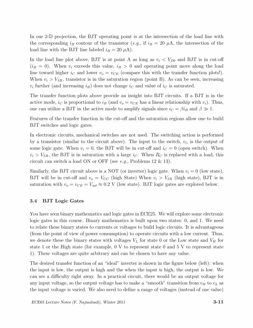
In our 2-D projection, the BJT operating point is at the intersection of the load line with
the corresponding iB contour of the transistor (e.g., if iB = 20 µA, the intersection of the
load line with the BJT line labeled iB = 20 µA).
In the load line plot above, BJT is at point A as long as vi < VD0 and BJT is in cut-off
(iB = 0). When vi exceeds this value, iB > 0 and operating point move along the load
line toward higher iC and lower vo = vCE (compare this with the transfer function plots!).
When vi > VIH , transistor is in the saturation region (point B). As can be seen, increasing
vi further (and increasing iB) does not change iC and value of iC is saturated.
The transfer function plots above provide an insight into BJT circuits. If a BJT is in the
active mode, iC is proportional to iB (and vo = vCE has a linear relationship with vi). Thus,
one can utilize a BJT in the active mode to amplify signals since iC = βiB and β ≫ 1.
Features of the transfer function in the cut-off and the saturation regions allow one to build
BJT switches and logic gates.
In electronic circuits, mechanical switches are not used. The switching action is performed
by a transistor (similar to the circuit above). The input to the switch, vi, is the output of
some logic gate. When vi = 0, the BJT will be in cut-off and iC = 0 (open switch). When
vi > VIH , the BJT is in saturation with a large iC . When RC is replaced with a load, this
circuit can switch a load ON or OFF (see e.g., Problems 12 & 13).
Similarly, the BJT circuit above is a NOT (or inverter) logic gate. When vi = 0 (low state),
BJT will be in cut-off and vo = VCC (high State) When vi > VIH (high state), BJT is in
saturation with vo = vCE = Vsat ≈ 0.2 V (low state). BJT logic gates are explored below.
3.4 BJT Logic Gates
You have seen binary mathematics and logic gates in ECE25. We will explore some electronic
logic gates in this course. Binary mathematics is built upon two states: 0, and 1. We need
to relate these binary states to currents or voltages to build logic circuits. It is advantageous
(from the point of view of power consumption) to operate circuits with a low current. Thus,
we denote these the binary states with voltages VL for state 0 or the Low state and VH for
state 1 or the High state (for example, 0 V to represent state 0 and 5 V to represent state
1). These voltages are quite arbitrary and can be chosen to have any value.
The desired transfer function of an “ideal” inverter is shown in the figure below (left): when
the input is low, the output is high and the when the input is high, the output is low. We
can see a difficulty right away. In a practical circuit, there would be an output voltage for
any input voltage, so the output voltage has to make a “smooth” transition from vH to vL as
the input voltage is varied. We also need to define a range of voltages (instead of one value)
ECE65 Lecture Notes (F. Najmabadi), Winter 2011 3-11

to represent high and low states as it is extremely difficult to design an electronic circuit to
give an exact voltage value. So, gates are designed to respond to a range of voltages, i.e.,
the gate would think that the input is low if the input voltage is smaller than VIL and would
think that the input is high if the input voltage is larger than VIH (see figure).
With these definitions, the transfer function of a practical inverter is shown below (right).
The range of voltages, VL to VIL and VIH to VH are called the noise margin(s). The range of
voltages between VIL to VIH is the forbidden region as in this range the output of the gate
does not correspond to a binary state. The maximum speed that a logic gate can operate is
set by the time it takes the circuit to traverse this forbidden region as the input voltage is
varied from one state to another state.
vo
vi
HV
V
VL
H
L V
vo
viV
V V V V
VH
L
L IL IH H
3.4.1 Resistor-Transistor Logic (RTL)
The transfer function of the common-emitter configuration is reproduced below. Comparing
this transfer function with the transfer function of a NOT gate (above), we can see the circuit
would acts as a NOT gate (or an inverter) with a low state of VL = Vsat and a high state of
VH = VCC with VIL = VD0 and VIH defined in page 3-10.
iv
vo
CC
C
B
V
R
R
vo
IH
sat
D0
vi
CC
activecut−off saturation
V
V
V
V
This circuit is a member of resistor-transistor (RTL) family of logic gates.
A major drawback of this RTL inverter gate is the limited input range for the “low” signal
(VIL). While the noise margin for the “high” state can be controlled by adjusting values of
ECE65 Lecture Notes (F. Najmabadi), Winter 2011 3-12

RC and RB, the noise margin for the “low” state is quite small and is set by VL = Vsat = 0.2 V
and VIL = VD0 = 0.7 V. Moreover, we have used a constant-voltage model for the BE junction
diode which assumes that BE junction turns ON at VD0 = 0.7 V. In reality, the BJT will
come out of cut-off (the BE junction will conduct) at smaller voltages (∼ 0.5 V), making
the noise margin for “low” state even smaller. Note that this issue of noise margin equally
applies to BJT switches.
In order to build a gate with a larger noise margin for the “low” state, we examine the
BE-KVL: vi = RBiB + vBE. Note that vi = VIL corresponds to vBE = VD0 and iB > 0 but
small. Two approaches are possible. First, we can add an element in series with RB which
would have a large voltage drop for a small current, e.g., a diode.
vo
CC
C
Biv
V
R
R
For this circuit, BE-KVL gives: vi = vD + RBiB + vBE. Then
to find VIL, we substitute for vBE = VD0 and iB > 0 but small
to get: VIL ≈ vD + VD0. Since iD = iB > 0 but small, the
diode should also be forward biased and vD = VD0. Thus,
VIL ≈ 2VD0 = 1.4 V. Note that VIL can be increased further in
increments of VD0 by adding more diodes in the input.
This approach works reasonably well in ICs as the diode and the BE junction can be con-
structed with similar reverse saturation currents. However, for a circuit built with discrete
components (e.g., a BJT switch) this approach may not work well as the reverse saturation
current for discrete diodes, is typically 2 to 3 orders of magnitude larger than reverse satu-
ration current for the BE junction. As such, the small current needed to make vBE ≃ VD0
only leads to vD = 0.3− 0.4 V. (see Lab 4 for a solution to this problem).
CC
Cvo
i2
iCiB
B
i1
1
iv
V
R
R
R
The second way to increase the noise margin is to add a resistor
between the base and ground as is shown. To see the impact
of this resistor, note that VIL is the input voltage when BJT is
just leaving the cut-off region. At this point, vBE = VD0, and iBis positive but very small (effectively zero). Since a voltage vBE
has appeared across R1, we have:
i1 =vBE
R1
i2 = iB + i1 ≈ i1 =vBE
R1
VIL = vi = RBi2 + vBE = vBERB
R1
+ vBE = VD0
(
1 +RB
R1
)
This value should be compared with VIL = VD0 in the absence of resistor R1. It can be seen
that for RB = R1, VIL can be raised from 0.7 to 1.4 V. Moreover, arbitrary values of VIL can
be achieved by proper choice of RB and R1. Typically, R1 does not affect VIH as iB needed
to put the BJT in saturation is typically several times larger than i1.
ECE65 Lecture Notes (F. Najmabadi), Winter 2011 3-13

RTL NOR Gate
All high-level logic gate can be constructed from “basic” logic gates like NOR or NAND.
By combining two or more RTL inverters, one obtains the basic logic gate circuit of RTL
family, a “NOR” gate, as is shown below left (see Problem 15). More BJTs can be added
for additional input signals. A RTL NAND gate is shown below right (see Problem 16).
Bi1vvo
CC
C
Bi2v
R
V
R
R
vo
C
Bi1v
Bi2v
CC
R
R
R
V
RTLs were the first digital logic circuits using transistors. They require at least one resistor
and one BJT per input. They were replaced with diode-transistor logic, DTL (reduced
number of resistors and BJTs) and transistor-transistor logic, TTL (which “packs” all of the
didoes in a special transistor). With the advent of CMOS technology, almost digital gates
are CMOS gates and BJTs are only used in high-speed emitter-coupled logic (ECL) circuits.
A DTL circuit is analyzed in the following section is as it provides a good example for solving
BJT circuits.
3.4.2 Diode-Transistor Logic (DTL)
The basic gate of DTL logic circuits is a NAND gate which is constructed by a combination
of a diode AND gate (analyzed in pages 2-12) and a BJT inverter gate as is shown below
(left figure). Because RB is large, on ICs, this resistor is usually replaced with two diodes.
The combination of the two diodes and the BE junction diode leads to a voltage of 2.1 V
for the inverter to switch and a VIL = 1.4 V for the NAND gate (Why?). Resistor R1 is
necessary because without this resistor, current iB will be too small and the voltage across
D3 and D4 will not reach 0.7 V although they are both forward biased.
Example: Verify that the DTL circuit above (with RA = 5 kΩ, RC = 1 kΩ, R1 = 5 kΩ,
and VCC = 5 V) is a NAND gate. Assume that “low”state is 0.2 V, “high” state is 5 V, and
BJT βmin = 40.
ECE65 Lecture Notes (F. Najmabadi), Winter 2011 3-14

1
2
RCRA
iB
RB
o
2
1
2
1
CC
A
3
D
Di
i
iv
v
v
V
v
RA
2
1
2
1
R1
RC
o
CC
3 41
24
5
A
3
iB
i
i D DD
D ii
i
v
v
v
V
v
Case 1: v1 = v2 = 0.2 V It appears that D1 and D2 will be forward biased by the 5-V
supply. Assume D1 and D2 are ON: vD1 = vD2 = VD0 = 0.7 V and i1 > 0, i2 > 0.
v3 = v1 + vD1 = v2 + vD2 = 0.2 + 0.7 = 0.9 V
Voltage v3 = 0.9 V is not sufficient to froward bias D3 and D4 as v3 = vD3+vD4+vBE and we
need at least 1.4 V to forward bias the two diodes. So both D3 and D4 are OFF and i4 = 0.
(Note that D3 and D4 can be forward biased without the BE junction being forward biased
as long as the current i4 is small enough such that voltage drop across the 5 kΩ resistor
parallel to the BE junction is smaller than 0.7 V. In this case, i5 = i4 and iB = 0.) Then:
i1 + i2 = iA =5− v35, 000
=5− 0.9
5, 000= 0.82 mA
And by symmetry, i1 = i2 = 0.5iA = 0.41 mA. Since both i1 and i2 are positive, our
assumption of D1 and D2 being ON are justified. Since i4 = 0, iB = 0 and BJT will be in
cut-off with iC = 0 and vo = 5 V.
So, in this case, D1 and D2 are ON, D3 and D4 are OFF, BJT is in cut-off, and vo = 5 V.
Case 2: v1 = 0.2 V, v2 = 5 V Following arguments of case 1, assume D1 is ON. Again,
v3 = 0.7+ 0.2 = 0.9 V, and D3 and D4 will be OFF with i4 = 0. We find that voltage across
D2 is vD2 = v3 − v2 = 0.9− 5 = −4.1 V and, thus, D2 will be OFF and i2 = 0. Then:
i1 = iA =5− v35, 000
=5− 0.9
5, 000= 0.82 mA
and since i1 > 0, our assumption of D1 ON is justified. Since i4 = 0, iB = 0 and BJT will
be in cut-off with iC = 0 and vo = 5 V.
So, in this case, D1 is ON, D2 is OFF, D3 and D4 are OFF, BJT is in cut-off, and vo = 5 V.
ECE65 Lecture Notes (F. Najmabadi), Winter 2011 3-15
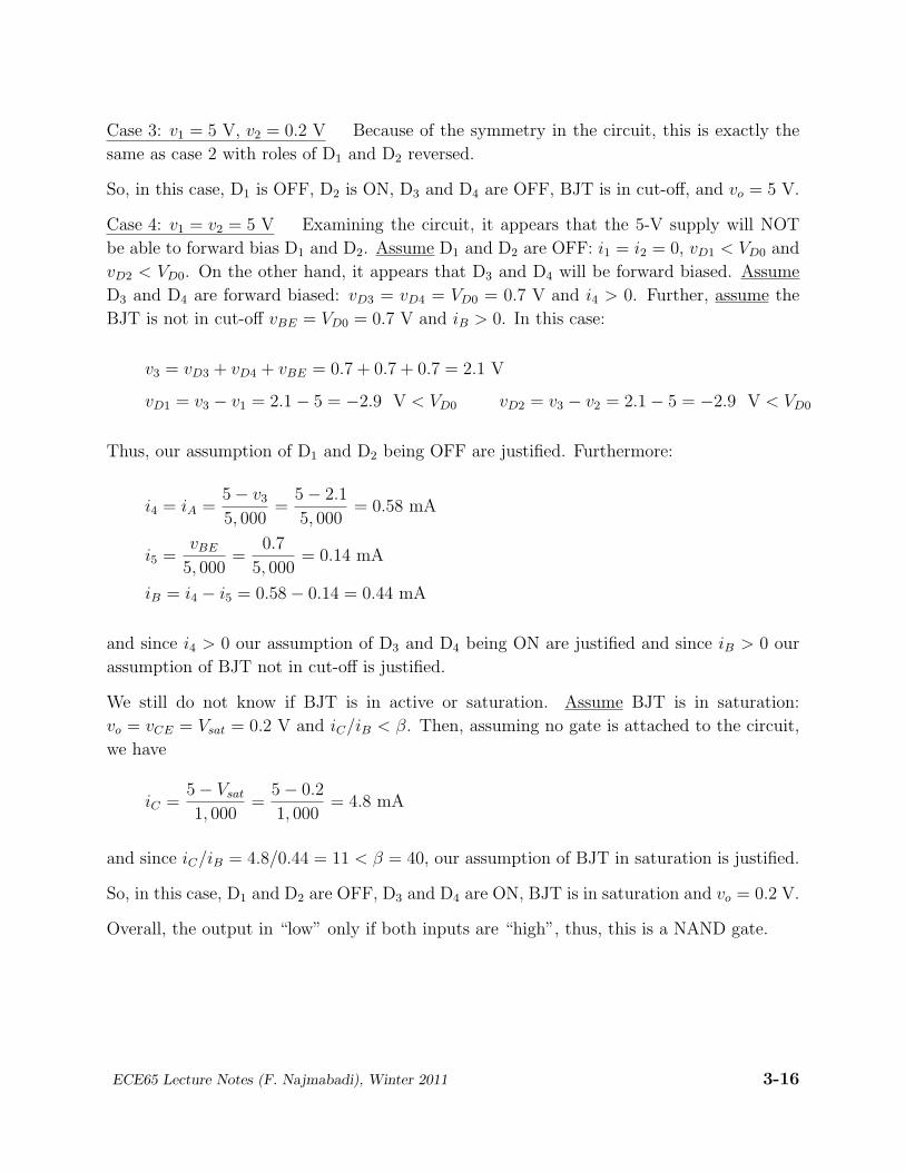
Case 3: v1 = 5 V, v2 = 0.2 V Because of the symmetry in the circuit, this is exactly the
same as case 2 with roles of D1 and D2 reversed.
So, in this case, D1 is OFF, D2 is ON, D3 and D4 are OFF, BJT is in cut-off, and vo = 5 V.
Case 4: v1 = v2 = 5 V Examining the circuit, it appears that the 5-V supply will NOT
be able to forward bias D1 and D2. Assume D1 and D2 are OFF: i1 = i2 = 0, vD1 < VD0 and
vD2 < VD0. On the other hand, it appears that D3 and D4 will be forward biased. Assume
D3 and D4 are forward biased: vD3 = vD4 = VD0 = 0.7 V and i4 > 0. Further, assume the
BJT is not in cut-off vBE = VD0 = 0.7 V and iB > 0. In this case:
v3 = vD3 + vD4 + vBE = 0.7 + 0.7 + 0.7 = 2.1 V
vD1 = v3 − v1 = 2.1− 5 = −2.9 V < VD0 vD2 = v3 − v2 = 2.1− 5 = −2.9 V < VD0
Thus, our assumption of D1 and D2 being OFF are justified. Furthermore:
i4 = iA =5− v35, 000
=5− 2.1
5, 000= 0.58 mA
i5 =vBE
5, 000=
0.7
5, 000= 0.14 mA
iB = i4 − i5 = 0.58− 0.14 = 0.44 mA
and since i4 > 0 our assumption of D3 and D4 being ON are justified and since iB > 0 our
assumption of BJT not in cut-off is justified.
We still do not know if BJT is in active or saturation. Assume BJT is in saturation:
vo = vCE = Vsat = 0.2 V and iC/iB < β. Then, assuming no gate is attached to the circuit,
we have
iC =5− Vsat
1, 000=
5− 0.2
1, 000= 4.8 mA
and since iC/iB = 4.8/0.44 = 11 < β = 40, our assumption of BJT in saturation is justified.
So, in this case, D1 and D2 are OFF, D3 and D4 are ON, BJT is in saturation and vo = 0.2 V.
Overall, the output in “low” only if both inputs are “high”, thus, this is a NAND gate.
ECE65 Lecture Notes (F. Najmabadi), Winter 2011 3-16

3.5 Exercise Problems
Problems 1 to 6. Find the transistor parameters (Si BJTs with β = 100).
Problem 7. Find I (Si BJT with β = 100).
2 mA
2.5 mA
µ20 A
+
−4 V
100 Aµ +
−
5 V+
+
−
−
4 V
1 V
Problem 1 Problem 2 Problem 3 Problem 4
1M
15 V
4.7 k
15 V
3.9k220k
15 V−1k15 V
I
1k
Problem 5 Problem 6 Problem 7
Problem 8. This configuration is called a Darlington Pair. A) Show that If Q1 is OFF,
Q2 will be OFF and if Q1 is ON, Q2 will ON, B) Show that if both BJTs are in active, the
transistor pair act like one BJT in active with β = iC2/iB1 ≈ β1β2.
Problems 9 and 10. Find iB, vBE, iC , vCE, and state of both transistors (Si BJTs with
β = 100).
Q1
Q2
1.3 M
10k
1kQ1
Q2
15 V
Q2
Q1
1k
1.5 M
15 V
Problem 8 Problem 9 Problem 10
Problem 11. Find iB, vBE, iC , vCE, and state of both transistors for A) vi = 1 V, B)
vi = 3 V, C) vi = 5 V. Si BJTs with β1 = 100 and β2 = 50.
ECE65 Lecture Notes (F. Najmabadi), Winter 2011 3-17

Problem 12.This is a switching circuit. vi is the output of a logic gate which turns the
light-emitting diode (LED) on or off depending on the state of the logic gate. The LED is
made of GaAs and has a VD0 = 1.7 V. A) Show that for vi = 0, LED will be OFF, B) Show
that for vi = 5 V, LED will be ON, and C) If we tarting from vi = 0 and slowly increase vi,
at what voltage LED starts to light up? (Si BJT with β = 100.)
Problem 13. Design a switch circuit similar to problem 12 which turns an LED OFF and
ON such that the LED is OFF for vi < 2.5 V and is ON for vi > 2.5 V. (Hint: See page 3-13
of lecture notes).
Problem 14. Show that this is NOR gate with a LOW state of 0.2 V and a HIGH state of
5 V (Si BJTs with β = 100).
Problem 15. Show that this is NAND gate with a LOW state of 0.4 V and a HIGH state
of 1.2 V (Si BJTs with β = 200).
3V
470
Q1
Q2
4.7k
470k
10V
iv
1k
47k
5Vvo
1v
2v
Q1
5k
500
5V
Q2
5k
vo
1v
2v
Q1
Q2
2k
2k
1k
1.2V
Problem 11 Problem 12 Problem 14 Problem 15
ECE65 Lecture Notes (F. Najmabadi), Winter 2011 3-18

3.6 Solution to Selected Exercise Problems
Problem 1. Find the transistor parameters (Si BJTs with β = 100).
2 mA
2.5 mA
This is a NPN transistor with iC = 2 mA and iE = 2.5 mA.
iB = iE − iC = 0.5 mA > 0 → BJT is ON → vBE = 0.7 V
iCiB
=2
0.5= 4 < 100 = β → BJT is in saturation → vCE = 0.2 V
Problem 2. Find the transistor parameters (Si BJTs with β = 100).
µ20 A
+
−4 V
This is a PNP transistor with iB = 20 µA and vCB = −4 V.
Since iB > 0, EB is ON and vEB = 0.7 V.
Since vCB = −4 < VD0 = 0.7 V, CB is reverse biased and this transistor is in active mode:
vEC = vEB + vBC = 0.7 + 4 = 4.7 V
iC = βiB = 2 mA
Problem 3. Find the transistor parameters (Si BJTs with β = 100).
100 Aµ +
−
5 V
This is a NPN transistor with iB = 100 µA and vCE = 5 V.
iB = 100 µ A > 0 → BJT is ON → vBE = 0.7 V
vCE = 5 V > VD0 = 0.7 V → BJT is in active → iC = βiB = 10 mA
Problem 4. Find the transistor parameters (Si BJTs with β = 100).
+
+
−
−
4 V
1 VThis is a PNP transistor with vEB = −1 V and vCB = −4 V.
vEB = −1 V < 0.7 = VD0 → BJT is in cut-off → iB = 0 & iC = 0
vEC = vEB + vBC = −1 + 4 = 3 V
ECE65 Lecture Notes (F. Najmabadi), Winter 2011 3-19
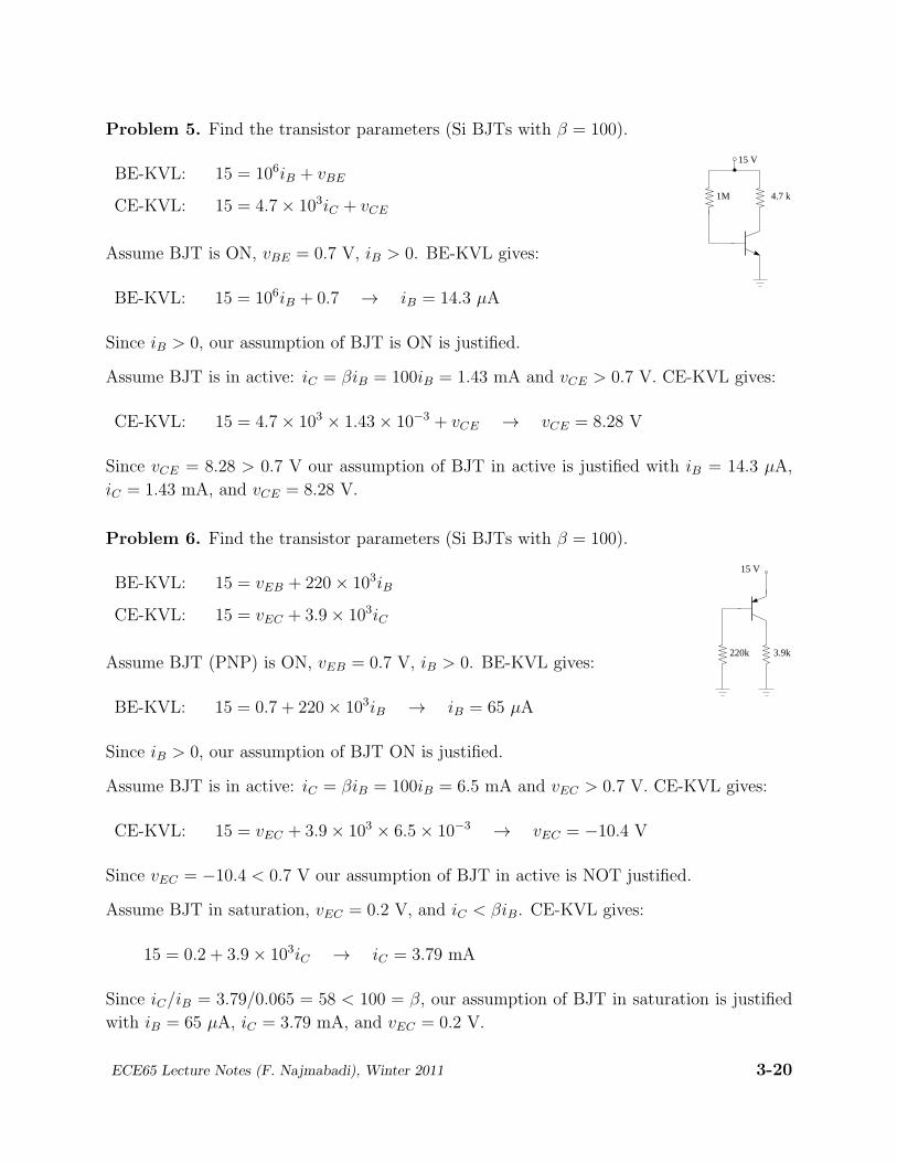
Problem 5. Find the transistor parameters (Si BJTs with β = 100).
1M
15 V
4.7 k
BE-KVL: 15 = 106iB + vBE
CE-KVL: 15 = 4.7× 10³iC + vCE
Assume BJT is ON, vBE = 0.7 V, iB > 0. BE-KVL gives:
BE-KVL: 15 = 106iB + 0.7 → iB = 14.3 µA
Since iB > 0, our assumption of BJT is ON is justified.
Assume BJT is in active: iC = βiB = 100iB = 1.43 mA and vCE > 0.7 V. CE-KVL gives:
CE-KVL: 15 = 4.7× 103 × 1.43× 10−3 + vCE → vCE = 8.28 V
Since vCE = 8.28 > 0.7 V our assumption of BJT in active is justified with iB = 14.3 µA,
iC = 1.43 mA, and vCE = 8.28 V.
Problem 6. Find the transistor parameters (Si BJTs with β = 100).
15 V
3.9k220k
BE-KVL: 15 = vEB + 220× 103iB
CE-KVL: 15 = vEC + 3.9× 10³iC
Assume BJT (PNP) is ON, vEB = 0.7 V, iB > 0. BE-KVL gives:
BE-KVL: 15 = 0.7 + 220× 103iB → iB = 65 µA
Since iB > 0, our assumption of BJT ON is justified.
Assume BJT is in active: iC = βiB = 100iB = 6.5 mA and vEC > 0.7 V. CE-KVL gives:
CE-KVL: 15 = vEC + 3.9× 103 × 6.5× 10−3→ vEC = −10.4 V
Since vEC = −10.4 < 0.7 V our assumption of BJT in active is NOT justified.
Assume BJT in saturation, vEC = 0.2 V, and iC < βiB. CE-KVL gives:
15 = 0.2 + 3.9× 10³iC → iC = 3.79 mA
Since iC/iB = 3.79/0.065 = 58 < 100 = β, our assumption of BJT in saturation is justified
with iB = 65 µA, iC = 3.79 mA, and vEC = 0.2 V.
ECE65 Lecture Notes (F. Najmabadi), Winter 2011 3-20

Problem 7. Find I (Si BJTs with β = 100).
15 V−1k15 V
I
1kBE-KVL: 15 = 103iE − vBE
CE-KVL: 15 = 103iE − vCE + 103iC − 15
Assume BJT (NPN) is OFF, iB = iC = iE = 0 and −vBE < 0.7 V. BE-KVL gives:
BE-KVL: 15 = −vBE
Since −vBE = 15 > 0.7 V, BJT is NOT in cut-off.
Assume BJT is ON, vBE = −0.7 V, iB > 0. BE-KVL gives:
BE-KVL: 15 = 103iE − (−0.7) → iE = 14.3 mA
Assume BJT is in active: iE ≈ iC = βiB and −vCE > 0.7 V. Therefore iC ≈ iE = 14.3 mA
and iB = iC/100 = 143 µA. CE-KVL gives
CE-KVL: 15 = 103 × 14.3× 10−3− vCE + 103 × 14.3× 10−3
− 15 → vCE = −1.4 V
Since −vCE = 1.4 > 0.7 V, BJT is in active with iB = 143 µA, iC = 14.3 mA, and
vCE = −1.4V.
Problem 8. This configuration is called a Darlington Pair. A) Show that If Q1 is OFF,
Q2 will be OFF and if Q1 is ON, Q2 will ON, B) Show that if both BJTs are in active, the
transistor pair act like one BJT in active with β = iC2/iB1 ≈ β1β2.
Q1
Q2
Darlington pair are arranged such that iE1 = iB2.
Part A:
If Q1 is OFF, iB1 = iC1 = iE1 = 0. Because of Darlington
pair arrangement, iB2 = iE1 = 0 and Q2 would also be OFF.
If Q1 is ON, iE1 > 0. Because of Darlington pair arrange-
ment, iB2 = iE1 > 0 and Q2 would also be ON.
Part B:
If Q1 & Q2 are both in active:
iC2 = β2iB2 = β2iE1 ≈ β2iC1 = β1β2iB1 →iC2
iB1
= β1β2
So, the Darlington pair act as a super high β BJT.
ECE65 Lecture Notes (F. Najmabadi), Winter 2011 3-21

Problem 9. Find iB, vBE, iC , vCE, and state of both transistors (Si BJTs with β = 100).
i11.3 M
10k
1kQ1
Q2
15 V
BE1-KVL: 15 = 1.3× 10⁶iB1 + vBE1
CE1-KVL: 15 = 10× 103i1 + vCE1
BE2-KVL: vCE1 = vBE2 + 103iE2
CE2-KVL: 15 = vCE2 + 103iE2
KCL: i1 = iC1 + iB2
Assume Q1 is ON, VBE1 = 0.7 V and iB1 > 0. BE1-KVL gives:
BE1-KVL: 15 = 1.3× 10⁶iB1 + 0.7 → iB1 = 11 µA
Since iB1 > 0, our assumption of Q1 ON is justified.
Assume Q1 is active, iC1 = 100iB1 = 1.1 mA and vCE1 > 0.7 V. In principle, we should move
forward and assume state of Q2 and solve the remaining three equations together. However,
solution can be simplified if we assume iB2 ≪ iC1 and check this assumption after solution.
If iB2 ≪ iC1, then i1 ≈ iC1. CE1-KVL gives:
CE1-KVL: 15 = 10× 103iC1 + vCE1 = 10× 103 × 1.1× 10−3 + vCE1 → vCE1 = 3.9 V
Since vCE1 > 0.7 V, our assumption of Q1 in active is correct. State of Q2 can be found
from BE2-KVL and CE2-KVL. Assume Q2 active: VBE2 = 0.7 V, iB2 > 0, iC2 = 100iB2,
and vCE2 > 0.7 V. Then iE2 ≈ iC2 and:
BE2-KVL: vCE1 = vBE2 + 103iE2
3.9 = 0.7 + 103iC2 → iC2 = 3.2 mA
CE2-KVL: 15 ≈ vCE2 + 103iC2 = vCE2 + 103 × 3.2× 10−3→ vCE2 = 11.8 V
Since vCE2 > 0.7 V, our assumption of Q2 in active is correct. Then iB2 = iC2/100 = 32 µA.
We note that iB2 = 32 µA ≪ iC1 = 1.1 mA. Therefore that assumption was also correct.
In sum, bot BJTs are in active and vBE1 = 0.7 V, iB1 = 11 µA, iC1 = 1.1 mA, vCE1 = 3.9 V,
vBE2 = 0.7 V, iB2 = 32 µA, iC2 = 3.2 mA, vCE2 = 11.8 V.
ECE65 Lecture Notes (F. Najmabadi), Winter 2011 3-22

Problem 10. Find iB, vBE, iC , vCE, and state of both transistors (Si BJTs with β = 100).
Q2
Q1
1k
1.5 M
15 V
Note that Q2 is a PNP transistor
BE1-KVL: 15 = 1.5× 10⁶iB1 + vBE1
CE1-KVL & BE2-KVL: 15 = vEB2 + vCE1
CE2-KVL: 15 = vEC2 + 103iC2
KCL: iC1 = iB2
Assume Q1 is ON, vBE1 = 0.7 V and iB1 > 0. BE1-KVL gives:
BE1-KVL: 15 = 1.5× 10⁶iB1 + 0.7 → iB1 = 9.5 µA
Since iB1 > 0, our assumption of Q1 ON is correct. Also, since iB2 = iC1 > 0, Q2 is ON and
vEB2 = 0.7 V. Then CE1-KVL gives vCE1 = 14.3 V. Since vCE1 > 0.7 V, Q1 is in active and
iC1 = 100iB1 = 0.95 mA.
KCL gives iB2 = iC1 = 0.95 mA. Assume Q2 is in active: iC2 = 100iB2 = 95 mA and
vEC2 > 0.7 V. CE2-KVL gives
CE2-KVL: 15 = vEC2 + 103iC2 = vEC2 + 103 × 95× 10−3→ vEC2 = −80 V
Since vEC2 = −80 < 0.7 V, our assumption of Q2 in active is incorrect. Assume Q2 is in
saturation: vEC2 = 0.2 V and iC2/iB2 < 100. CE2-KVL gives:
CE2-KVL: 15 = vEC2 + 103iC2 = 0.2 + 103iC2 → iC2 = 14.8 mA
Since iC2/iB2 = 14.8/0.95 = 15.6 < 100, our assumption of Q2 in saturation is correct.
In sum, Q1 is in active, Q2 is in saturation, and vBE1 = 0.7 V, iB1 = 9.5 µA, iC1 = 0.95 mA,
vCE1 = 14.3 V, vEB2 = 0.7 V, iB2 = 0.95 mA, iC2 = 14.8.2 mA, vEC2 = 0.2 V.
ECE65 Lecture Notes (F. Najmabadi), Winter 2011 3-23

Problem 11. Find iB, vBE, iC , vCE, and state of both transistors for A) vi = 1 V, B)
vi = 3 V, C) vi = 5 V. Si BJTs with β1 = 100 and β2 = 50.
3V
470
Q1
Q2
4.7k
470k
10VNote that BJTs are arranged as a Darlington pair with
iE1 = iB2. So they will be either both ON or both OFF.
BE1-KVL: Vi = 470× 103iB1 + vBE1 + vBE2
CE1-KVL & BE2-KVL: 10 = 4.7× 10³iC1 + vCE1 + vBE2
CE2-KVL: 10 = 470iC2 + vCE2
KCL: iC1 = iB2
Part A: vi = 1 V.
Assume both BJTs are ON: vBE1 = vBE2 = 0.7 V, iB1 > 0, and iB2 > 0. BE1-KVL gives:
BE1-KVL: 1 = 470× 103iB1 + 0.7 + 0.7 → iB1 = −0.8 µA
Since iB1 < 0, our assumption is incorrect and both BJTs are in cut-off with iB1 = iC1 =
iB2 = iC2 = 0. CE2-KVL gives vCE2 = 10 V. CE1-KVL gives vCE1 + vBE2 = 10 V. Our
simple large-signal model for the BJT cannot resolve the values of vCE1 and vBE2 because any
values of vBE2 < 0.7V and the corresponding value of vCE1 = 10− vBE2 will be acceptable.
The problem of not finding unique values for vCE1 and vBE2 is due to our simple diode model
of the BE junction. In reality both BE junctions will be forward biased with voltages smaller
than 0.7 V (so both iB’s will be very small) and BJTS will have small values of iC ’s.
Part B: vi = 3 V.
Assume both BJTs are ON: vBE1 = vBE2 = 0.7 V, iB1 > 0, and iB2 > 0. BE1-KVL gives:
BE1-KVL: 3 = 470× 103iB1 + 0.7 + 0.7 → iB1 = 3.4 µA
Since iB1 > 0, our assumption is correct and both BJTs are ON.
Assume Q1 in active: iC1 = 100iB1 = 0.34 mA and vCE1 > 0.7 V. Then CE1-KVL gives:
CE1-KVL & BE2-KVL: 10 = 4.7× 10³iC1 + vCE1 + vBE2
10 = 4.7× 103 × 0.34× 10−3 + vCE1 + 0.7 → vCE1 = 7.7 V
ECE65 Lecture Notes (F. Najmabadi), Winter 2011 3-24

Since vCE1 = 7.7 > 0.7 V, our assumption of Q1 in active is correct. Then, iB2 = iE1 ≈
iC1 = 0.34 mA.
Assume Q2 is in active: iC2 = 50iB2 = 17 mA and vCE2 > 0.7 V. Then CE2-KVL gives:
CE2-KVL: 10 = 470iC2 + vCE2 = 470× 17× 10−3 + vCE2 → vCE2 = 2.01 V
Since vCE2 = 2.01 > 0.7 V, our assumption of Q2 in active is correct.
Therefore, Q1 & Q2 are in active, and vBE1 = vBE2 = 0.7 V, iB1 = 3.4 µA, iC1 = 0.34 mA,
vCE1 = 7.7 V, iB2 = 0.34 mA, iC2 = 17 mA, and vCE2 = 2.01 V.
Part C: vi = 5 V.
Assume both BJTs are ON: vBE1 = vBE2 = 0.7 V, iB1 > 0, and iB2 > 0. BE1-KVL gives:
BE1-KVL: 5 = 470× 103iB1 + 0.7 + 0.7 → iB1 = 7.66 µA
Since iB1 > 0, our assumption is correct and both BJTs are ON.
Assume Q1 is in active: iC1 = 100iB1 = 0.77 mA and vCE1 > 0.7 V. Then CE1-KVL gives:
CE1-KVL & BE2-KVL: 10 = 4.7× 10³iC1 + vCE1 + vBE2
10 = 4.7× 103 × 0.77× 10−3 + vCE1 + 0.7 → vCE1 = 5.70 V
Since vCE1 = 5.70 > 0.7 V, our assumption of Q1 in active is correct. Then, iB2 = iE1 ≈C1=
0.77 mA.
Assume Q2 is in active: iC2 = 50iB2 = 38.3 mA and vCE2 > 0.7 V. Then CE2-KVL gives:
CE2-KVL: 10 = 470iC2 + vCE2 = 470× 38.3× 10−3 + vCE2 → vCE2 = −8.0 V
Since vCE2 = −8.0 < 0.7 V, our assumption is incorrect and Q2 is in saturation: vCE2 = 0.2 V
and iC2/iB2 < 50. Then CE2-KVL gives:
CE2-KVL: 10 = 470iC2 + vCE2 = 470iC2 + 0.2 → iC2 = 20.9 mA
Since iC2/iB2 = 20.9/0.77 = 27 < 50, our assumption is correct.
Therefore, Q1 is in active, Q2 is in saturation, and vBE1 = vBE2 = 0.7 V, iB1 = 7.66 µA,
iC1 = 0.77 mA, vCE1 = 5.7 V, iB2 = 0.77 mA, iC1 = 20.9 mA, and vCE2 = 0.2 V.
ECE65 Lecture Notes (F. Najmabadi), Winter 2011 3-25

Problem 12. This is a switching circuit. vi is the output of a logic gate which turns the
light-emitting diode (LED) on or off depending on the state of the logic gate. The LED is
made of GaAs and has a VD0 = 1.7 V. A) Show that for vi = 0, LED will be OFF, B) Show
that for vi = 5 V, LED will be ON, and C) If we tarting from vi = 0 and slowly increase vi,
at what voltage LED starts to light up? (Si BJT with β = 100.)
iv
1k
47k
5VBE-KVL: vi = 47× 105iB + vBE
CE-KVL: 5 = 103iC + vD + vCE
iC = iD
Part A: vi = 0:
Assume BJT is OFF, iB = 0 and vBE < 0.7 V. BE-KVL gives:
BE-KVL: 0 = 47× 103iB + vBE = 0 + vBE → vBE = 0
Since vBE = 0 < 0.7 V, our assumption of BJT in cut-off is correct and iC = 0. Since
iD = iC = 0, the diode will be OFF.
Part B: vi = 5 V:
Assume BJT is ON, vBE = 0.7 V, iB > 0. BE-KVL gives:
BE-KVL: 5 = 47× 103iB + 0.7 → iB = 91.5 µA
Since iB > 0 our assumption of BJT is ON is justified. When BJT is ON, iC > 0 and since
iD = iC > 0, the LED will be on with vD = 1.7 V.
Assume BJT is in active: iC = βiB = 100iB = 9.15 mA and vCE > 0.7 V. CE-KVL gives:
CE-KVL: 5 = 103iC + vD + vCE
5 = 103 × 9.15× 10−3 + 1.7 + vCE → vCE = −5.85 V
Since vCE = −5.85 < 0.7 V our assumption of BJT in active is NOT justified.
Assume BJT in saturation, vCE = 0.2 V, and iC < βiB. CE-KVL gives:
CE-KVL: 5 = 103iC + vD + vCE = 103iC + 1.7 + 0.2 → iC = 3.1 mA
Since iC/iB = 3.1/0.0915 = 34 < 100 = β, our assumption of BJT in saturation is justified.
ECE65 Lecture Notes (F. Najmabadi), Winter 2011 3-26

Therefore, for vi = 5 V, LED is ON, BJT is in saturation, and vBE = 0.7 V, vD = 1.7 V,
iB = 91.5 µA, iC = 3.1 mA, and vCE = 0.2 V.
Part C:
LED is ON when iD > 0. Since iC = iD > 0, the BJT should be ON.
We found that for vi = 0, BJT is in cut-off and LED is OFF. As we increase vi and while
BJT is still in cut-off, BE-KVL gives vBE = vi since iB = 0. So as we increase vi, vBE
increases while iB remains zero.
When vi reaches 0.7 V, vBE also reaches 0.7 V while iB is still zero.
If we increase vi beyond this point, vBE cannot increase, rather iB becomes positive and BJT
will be turned ON leading to iC > 0 and LED turning ON.
So, LED will light up when vi ≥ 0.7 V.
Problem 13. Design a switch circuit similar to problem 12 which turns an LED OFF and
ON such that the LED is OFF for vi < 2.5 V and is ON for vi > 2.5 V. (Hint: See page 3-13
of lecture notes).
iv
iB
iR
1k
47k
5V
i
R
Addition of a resistor R (see circuit) will raise vi that turns the LED ON.
In problem 12, we saw that LED will just turn ON when
vBE = 0.7 V and iB ≈ 0. BE-KVL gives:
BE-KVL: vi = 47× 103i+ vBE
2.5 = 47× 105i+ 0.7 → i = 38.3 µA
Since iB = 0, iR = i = 38.3 µA. Ohm’s law for the resistor R gives:
vBE = RiR → 0.7 = 38.3× 10⁻⁶R → R = 18.3 kΩ
ECE65 Lecture Notes (F. Najmabadi), Winter 2011 3-27

Problem 14. Show that this is NOR gate with a LOW state of 0.2 V and a HIGH state of
5 V (Si BJTs with β = 100).
vo
1v
2v
Q1
5k
500
I
5V
Q2
5k
We first find the state of Q1 for the two cases of V1 = 0.2 and
5 V.
BE1-KVL: v1 = 500iB1 + vBE1
For v1 = 0.2 V, assume that Q1 is in cut-off (iB1 = 0 and
vBE1 < VD0 = 0.7 V). Then, BE1-KVL gives VBE1 = 0.2 < 0.7 V
and, thus, Q1 is indeed in cut-off. So:
v1 = 0.2 V → iB1 = iC1 = 0, vBE1 = 0.2 V, vCE1 can be anything
For v1 = 5 V, assume that Q1 is NOT in cut-off (iB1 > 0 and vBE1 = VD0 = 0.7 V).
Substituting for vBE1 = 0.7 in BE1-KVL, we get IB1 = 4.3/5, 000 = 0.86 mA. Since iB1 > 0,
Q1 is indeed NOT in cut-off. Therefore,
v1 = 5 V → BJT is ON (not in cut-off) iB1 = 0.86 mA vBE1 = 0.7 V iC1 > 0
Note that because the circuit is symmetric (i.e., there is no difference between Q1 circuit
and Q2 circuit), the above results also applies to Q2.
Case a: v1 = v2 = 0.2 V From above, both BJTs will be in cut-off and iC1 = iC2 = 0. By
KCL, I = iC1 + iC2 = 0, and vo can be found from Ohm’s Law:
5− vo = 500I = 0 → vo = 5 V
Case b: v1 = 0.2 V, v2 = 5 V Since v1 = 0.2 V, Q1 will be in cut-off with iC1 = 0. Since
v2 = 5 V, Q2 will not be in cut-off with iB2 = 0.86 mA. Assume Q2 is in saturation
(vCE2 = 0.2 V and iC2/iB2 < β). In this case, vo = vCE2 = 0.2 V and I = iC1 + iC2 = iC2.
By Ohm’s Law:
500I = 500iC2 = 5− Vo = 5− vCE2 = 4.8 → iC2 = 4.8/500 = 9.6 mA
Since iC2/iB2 = 11 < β = 100, Q2 is indeed in saturation. So, in this case, vo = 0.2 V.
Case c: v1 = 5, v2 = 0.2 V Because the circuit is symmetric (i.e., there is no difference
between Q1 circuit and Q2 circuit), results from Case b can be applied here. Thus, Q2 will be
in cut-off with iC2 = 0 and Q1 will be in saturation with iC1 = 9.6 mA and vo = vCE2 = 0.2 V.
ECE65 Lecture Notes (F. Najmabadi), Winter 2011 3-28

Case d: v1 = v2 = 5 V Both BJTs will be ON with iB1 = iB2 = 0.86 mA and vBE1 =
vBE2 = 0.7 V. Since from the circuit, vCE1 = vCE2, both BJTs will be in saturation or both
in active. Assume that both are in saturation. Then, vo = vCE1 = vCE2 = 0.2 V and we
should have iC1/iB1 < β and iC2/iB2 < β. By Ohm’s Law:
500I = 5− vo = 5− 0.2 = 4.8 → I = 4.8/500 = 9.6 mA
Since BJTs are identical and have same iB, we should have iC1 = iC2 and current I should
be equally divided between two BJTs. Thus, iC1 = iC2 = 0.5I = 4.8 mA. To check if BJTs
are in saturation: iC1/iB1 = 4.8/0.86 = 5 < β = 100 and iC2/iB2 = 4.8/0.86 = 5 < β = 100
so both BJTs are indeed in saturation and vo = 0.2 V.
In summary, the output is high when both inputs are low and the output is low otherwise.
Therefore, this is a NOR gate.
Problem 15. Show that this is NAND gate with a LOW state of 0.4 V and a HIGH state
of 1.2 V (Si BJTs with β = 200).
vo
1v
2v
Q1
Q2
2k
2k
1k
1.2V
iE1 = ic2
CE-KVL: 1.2 = 103iC1 + vCE1 + vCE2
vo = vCE1 + vCE2 = 1.2− 103iC1
BE1-KVL: v1 = 2× 10³iB1 + vBE1 + vCE2
BE2-KVL: v2 = 2× 10³iB2 + vBE2
Case 1: v1 = 0.4, v2 = 0.4: Assume Q2 is off (iB2 = 0, vBE2 < VD0). Substituting for iB2 = 0
in the BE2-KVL above, we get: vBE2 = v2 = 0.4 < 0.7 = VD0. Thus, Q2 is off and iC2 = 0.
Since iE1 = iC2 = 0 and iE1 = iC1 + iB1 = 0, we should have iC1 = 0 (because iC1 ≥ 0 and
iB1 ≥ 0) . Then, from CE-KVL above:
vo = 1.2− 103iC1 = 1.2 V
Case 2: v1 = 1.2, v2 = 0.4: Similar to Case 1, assume Q2 is off to find ic1 = 0 and vo = 1.2 V.
Case 3: v1 = 0.4, v2 = 1.2: Assume Q1 is off (iB1 = 0, vBE1 < VD0). Substituting for iB1 = 0
in the BE1-KVL above, we get: vBE1 = 0.4− vCE2. Since vCE2 cannot be negative (powered
by 1.2 V),vBE1 = 0.4− vCE2 < 0.7 = VD0 and Q1 is off (iC1 = 0). Then:
vo = 1.2− 103iC1 = 1.2 V
ECE65 Lecture Notes (F. Najmabadi), Winter 2011 3-29

Case 4: v1 = 1.2, v2 = 1.2: Since both inputs are high, we start by assuming that both
BJTs are ON (we still need to prove it): iB2 > 0, vBE2 = VD0 = 0.7 V and iB1 > 0,
vBE1 = VD0 = 0.7 V. Four possible combinations exist with Q1 and Q2 being respectively
in active & active, active & saturation, saturation & active, and saturation & active. Since
problem states that this is NAND gate and the low voltage is 0.4 V, a good guess is that
both BJTs are in saturation vCE1 = Vsat = 0.2 V, iC1/iB1 < β and vCE2 = Vsat = 0.2 V,
iC2/iB2 < β.
Starting with BE1-KVL and BE2-KVL above, we get:
1.2 = 2× 10³iB2 + 0.7 → iB2 = 0.25 mA
1.2 = 2× 10³iB1 + 0.7 + 0.2 → iB1 = 0.15 mA
Since iB2 > 0, and iB1 > 0, assumption of both BJTs ON is correct. Then, CE-KVL gives:
1.2 = 103iC1 + 0.2 + 0.2 → iC1 = 0.8 mA
Since iC1/iB1 = 0.8/0.15 = 5.3 < β = 200, our assumption of Q1 being in saturation
is justified. To find iC2, we note iC2 = iE1 = iC1 + iB1 = 0.8 + 0.15 = 0.95 mA. Then
iC2/iB1 = 0.95/0.25 = 3.8 < β = 200, so our assumption of Tr2 being in saturation is also
justified. Lastly,
vo = vCE1 + vCE2 = 0.2 + 0.2 = 0.4 V
Overall, vo = 1.2 V or HIGH State (cases 1, 2, and 3) unless both inputs are HIGH (case 4).
Therefore, this is a NAND gate.
ECE65 Lecture Notes (F. Najmabadi), Winter 2011 3-30