IGH-SPEED ITHIUM ION BATTERY CHARGER - Silicon Labs · PDF file · 2017-07-26note...
44
Rev. 1.3 7/13 Copyright © 2013 by Silicon Laboratories AN146 AN146 H IGH -S PEED L ITHIUM I ON B ATTERY C HARGER Introduction Driven by the need for untethered mobility and ease of use, many systems rely on rechargeable bat- teries as their primary power source. The battery charger is typically implemented using a fixed- function IC to control the charging current/voltage profile. The C8051F300 family provides a flexible alterna- tive to fixed-function linear battery chargers. This note discusses how to use the C8051F300 device in Li-Ion battery charger applications. The Li-Ion charging algorithms can be easily adapted to other battery chemistries. The code accompanying this application note was originally written for C8051F30x devices. The code can also be ported to other devices in the Sili- con Labs microcontroller range. Key Points • On-chip high-speed ADC provides superior accuracy in monitoring charge voltage (critical to prevent overcharging in Li-Ion applications), maximizing charge effectiveness and battery life. • On-chip comparator and PWM provides a means to implement a high speed buck con- verter with a small external inductor. • On-chip temperature sensor provides an accu- rate and stable drive voltage for determining battery temperature. An external RTD (resistive temperature device) can also be accommo- dated. • A single C8051F300 provides full product range for multi-chemistry chargers, expediting time to market and reducing inventory. Charging Basics Batteries are exhaustively characterized to deter- mine safe yet time-efficient charging profiles. The optimum charging method for a battery is depen- dent on the battery’s chemistry (Li-Ion, NiMH, NiCd, SLA, etc.). However, most charging strate- gies implement a 3-phase scheme: 1. Low-current conditioning phase 2. Constant-current phase 3. Constant-voltage phase/charge termination V Pos (+) V Neg (-) LED Buck Converter Sense Resistor Li-Ion Cells 8k FLASH, PWM, Temp Sensor, Precision Time Base 8051F300 Cygnal Integrated Products Resistor Divider LDO PWM Out AIN1 - Voltage AIN2 - Current Amplifier Figure 1. Lithium Ion Battery Charger Block Diagram.
Transcript of IGH-SPEED ITHIUM ION BATTERY CHARGER - Silicon Labs · PDF file · 2017-07-26note...

Rev. 1.3 7/13 Copyright © 2013 by Silicon Laboratories AN146
AN146
HIGH-SPEED LITHIUM ION BATTERY CHARGER
IntroductionDriven by the need for untethered mobility andease of use, many systems rely on rechargeable bat-teries as their primary power source. The batterycharger is typically implemented using a fixed-function IC to control the charging current/voltageprofile.
The C8051F300 family provides a flexible alterna-tive to fixed-function linear battery chargers. Thisnote discusses how to use the C8051F300 device inLi-Ion battery charger applications. The Li-Ioncharging algorithms can be easily adapted to otherbattery chemistries.
The code accompanying this application note wasoriginally written for C8051F30x devices. Thecode can also be ported to other devices in the Sili-con Labs microcontroller range.
Key Points• On-chip high-speed ADC provides superior
accuracy in monitoring charge voltage (critical to prevent overcharging in Li-Ion applications), maximizing charge effectiveness and battery life.
• On-chip comparator and PWM provides a means to implement a high speed buck con-verter with a small external inductor.
• On-chip temperature sensor provides an accu-rate and stable drive voltage for determining battery temperature. An external RTD (resistive temperature device) can also be accommo-dated.
• A single C8051F300 provides full product range for multi-chemistry chargers, expediting time to market and reducing inventory.
Charging BasicsBatteries are exhaustively characterized to deter-mine safe yet time-efficient charging profiles. Theoptimum charging method for a battery is depen-dent on the battery’s chemistry (Li-Ion, NiMH,NiCd, SLA, etc.). However, most charging strate-gies implement a 3-phase scheme:
1. Low-current conditioning phase
2. Constant-current phase
3. Constant-voltage phase/charge termination
V Pos (+)
V Neg (-)
LED
BuckConverter
Sense Resistor
Li-IonCells
8k FLASH, PWM,Temp Sensor,
Precision Time Base
8051F300
CygnalIntegratedProducts
ResistorDivider
LDO
PWM Out
AIN1 - Voltage
AIN2 - CurrentAmplifier
Figure 1. Lithium Ion Battery Charger Block Diagram.

AN146
2 Rev. 1.3
All batteries are charged by transferring electricalenergy into them. The maximum charge current fora battery is dependent on the battery’s rated capac-ity (C). For example, a battery with a cell capacityof 1000mAh is referred to as being charged at 1C(1 times the battery capacity) if the charge currentis 1000mA. A battery can be charged at 1/50C (20mA) or lower if desired. However, this is a com-mon trickle-charge rate and is not practical in fastcharge schemes where short charge-time is desired.
Most modern chargers utilize both trickle-chargeand rated charge (also referred to as bulk charge)while charging a battery. The trickle-charge currentis usually used in the initial phases of charging tominimize early self heating which can lead to pre-mature charge termination. The bulk charge is usu-ally used in the middle phase where the most of thebattery’s energy is restored.
During the final phase of battery charge, whichgenerally takes the majority of the charge time,either the current or voltage or a combination ofboth are monitored to determine when charging iscomplete. Again, the termination scheme dependson the battery’s chemistry. For instance, most Lith-ium Ion battery chargers hold the battery voltageconstant, and monitor for minimum current. NiCdbatteries use a rate of change in voltage or tempera-ture to determine when to terminate.
While charging, some of the electrical energy isconverted to thermal energy, until the batteryreaches full charge, at which time all the electricalenergy is converted to thermal energy. If chargingisn’t terminated, the battery can be damaged ordestroyed. Fast chargers (chargers that charge bat-teries fully in less than two hours) compound thisissue, as these chargers use a high charge current tominimize charge time. Therefore, monitoring a bat-tery’s temperature is critical especially for Li-Ionbatteries which may explode if overcharged. Tem-perature is monitored during all phases and chargeis terminated immediately if the temperatureexceeds a preset maximum limit.
Hardware DescriptionLi-Ion batteries are currently the battery chemistryof choice for most applications due to their highenergy/space and energy/weight characteristicswhen compared to other chemistries. Most modernlinear Li-Ion chargers use the tapered charge termi-nation, minimum current (see Figure 2) method toensure the battery is fully charged, as does theexample code provided at the end of this applica-tion note.
Buck ConverterThe most economical way to create a tapered ter-mination linear charger is to use a buck converter.A buck converter is a switching regulator that usesan inductor and/or a transformer (if isolation isdesired), as an energy storage element to transferenergy from the input to the output in discretepackets. Feedback circuitry regulates the energytransfer via the transistor, also referred to as thepass switch, to maintain a constant voltage or con-stant current within the load limits of the circuit.
AN146
Rev. 1.3 3
Charge Current
Charge Voltage
TimeConditioningPhase
Current regulation Voltage regulation
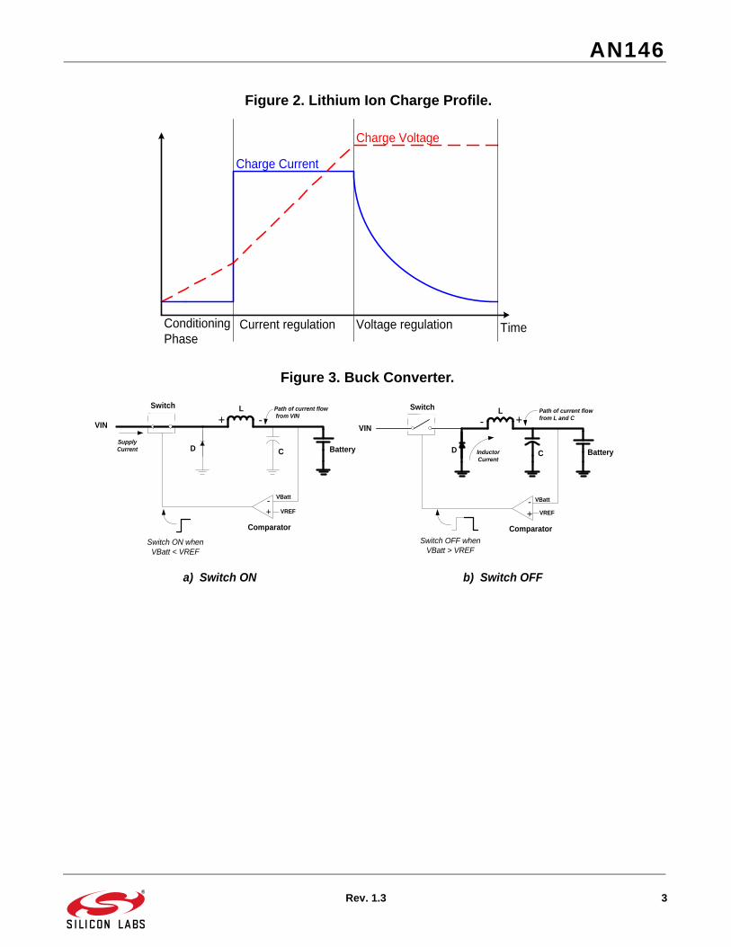
Figure 2. Lithium Ion Charge Profile.
-+ VREF
Switch
Comparator
D
L
C
VBatt
VIN
Path of current flowfrom L and C
Switch OFF whenVBatt > VREF
-+ VREF
Switch
Comparator
D
L
C
VBatt
VIN
Path of current flow from VIN
Switch ON whenVBatt < VREF
a) Switch ON b) Switch OFF
Battery Battery
+ - +-
InductorCurrent
SupplyCurrent
Figure 3. Buck Converter.

AN146
4 Rev. 1.3
Buck Regulator OperationThe buck regulator operates by controlling the dutycycle of a transistor switch. The duty cycle is auto-matically increased to dispense more current intothe battery. A comparator closes the switch whenVBATT < VREF. As shown in Figure 3a, currentflows into the battery and capacitor C. This currentis also stored in inductor L. VBATT rises until itexceeds VREF at which time the comparator turnsthe switch off (Figure 3b). The current stored in theinductor rapidly decreases until diode D is forwardbiased, causing inductor current to flow into thebattery at a decreasing rate. Capacitor C begins dis-charging after the inductor current has decayed andeventually VBATT begins to fall. When VBATT fallsbelow VREF, the comparator again turns the switchon and another cycle begins. On a larger scale, ifthe duty cycle is decreased (shorter “on” time), theaverage voltage decreases and vice versa. There-fore, controlling the duty cycle allows one to regu-late the voltage or the current to within desiredlimits.
Selecting the Buck Converter InductorTo size the inductor in the buck converter, one firstassumes a 50 percent duty cycle, as this is wherethe converter operates most efficiently.
Duty cycle is given by Equation 1, where T is theperiod of the PWM (in our example T = 10.5S).
With this established, select a PWM switching fre-quency. As Equation 2 shows, the larger the PWMswitching frequency, the smaller (and more costeffective) the inductor. Our example code config-
ures the ‘F300’s hardware to generate a 510kHzswitch rate.
Now we can calculate the inductor’s size. Assum-ing Vi, the charging voltage, is 15V, Vsat, the satu-ration voltage, is 0.5V, the desired output voltage,Vo, is 4.2V, and I0MAX, the maximum output cur-rent, is 1500 mA, the inductor should be at least4H.
Note that the capacitor in this circuit is simply aripple reducer. The larger it is the better as ripple isinversely proportional to the size of the capacitor.
High Speed ChargerAs AN037, Lithium Ion Battery Charger UsingC8051F300, illustrates, the F300’s 8-bit PWM canbe configured to generate a 96kHz PWM with noexternal components. This PWM output can beused to drive the pass switch in a buck converterand charge a battery. However, a 96kHz frequencyrequires a buck converter to utilize a relativelylarge 18H inductor. For some applications, this istoo large and costs too much. To reduce the sizeand cost of this inductor requires that the switchrate of the buck converter increase. The beauty ofthe F300 lies in its flexible feature set. As men-tioned, included in the device is a PCA (Program-mable Counter Array) that has three 16-bit capture/compare modules with corresponding output drivesthat can be configured to provide numerous func-tions. We can use two of the PCA’s modules, alongwith two external single-pole low-pass filters, andthe on-chip comparator to generate an 8-bit,510kHz PWM (refer to Figure 4 for details). Bysetting the switch rate to 510kHz, the inductorrequired to satisfy the buck converter equations isreduced by a factor of five to approximately 4H.
DutyCycletonT
---------=
Equation 1. Duty Cycle.
LVi Vsat– Vo– ton
2Iomax----------------------------------------------------=
Equation 2. Inductor Size.

AN146
Rev. 1.3 5
To create a 510kHz PWM with the F300, Module 0of the PCA is configured to provide a 510kHzsquare wave via the Frequency Output Mode. Thissquare wave is then filtered through a low-pass fil-ter with a 500kHz corner frequency to provideapproximately a 2 Volt peak-to-peak pseudo trian-gle wave to the positive input of the on-chip com-parator. For the minus input of the comparator,Module 1 is configured as an 8-bit PWM at 96kHzswitch rate. This PWM output is then low pass fil-tered with a corner frequency of approximately15Hz to create a simple DC digital-to-analog con-verter. By comparing the pseudo triangle wave to aDC input, the output of the comparator’s outputbecomes a 510kHz PWM.
The DC control path, Module1’s output in thisexample, controls the duty cycle of the 510kHzPWM output from the comparator. By varying theduty cycle of the 8-bit 96kHz PWM, the minusinput to the comparator can be varied from 0 voltsto the supply, typically 3.3V. The accuracy of theDC control path is limited by the settling time ofthe external RC filter. For this example, compo-nents were selected to minimize errors contributedfrom this path. For more details on componentselection for the DC path, refer to AN010, 16-BitPWM Using an On-Chip Timer.
The overall accuracy of the 510kHz PWM outputfrom the comparator is mostly limited by thepseudo triangle path to the comparator. Assumingthe DC path is error free, to create a true 8-bit510kHz PWM output from the comparator requiresthat a perfectly linear full-scale triangle wave beinput to the positive input of the comparator. A truefull scale triangle wave refers to a triangle wavethat linearly ramps from 0 volts to the positive sup-ply and then returns back the negative supply in asimilar fashion. However, the charge and dischargeprofile of a capacitor in the low pass configurationis not linear past a time constant. Moreover, it isdesirable not to allow this capacitor to fully chargeas the pseudo triangle wave becomes more nonlin-ear towards its peaks. Unfortunately, limiting theoverall charge time/voltage limits the overall accu-racy of the 510kHz PWM. For example, if we com-pare a triangle wave with a peak-to-peak voltage of1/4 the supply to the DC control path’s voltage, wecould generate a 2-bit 510kHz PWM output fromthe comparator. In practical applications, a 2-bit510kHz has very limited use. To improve the accu-racy requires either one of two changes: 1) increasethe voltage of the pseudo triangle wave or 2)increase the resolution of the DC path’s PWM con-trol. As mentioned earlier, increasing the peak-to-peak voltage of the pseudo triangle wave can beeasily accomplished by adjusting its low pass filtercomponents accordingly. Our example is designed
BuckConverter
C8051F300
Module1
Module0
Comparator
TBAT
VBAT
IBAT
CMP0
PseudoTriangleWave
DCControl
CEX1
CEX0
CMP+
CMP-
High Speed PWM
Figure 4. High Speed Charger.

AN146
6 Rev. 1.3
to provide approximately a 2 volt peak-to-peakpseudo triangle wave. When compared to the 8-bitPWM dc control path, we achieve approximately7.5-bits of performance at 510kHz switch rate.
The overall resolution of the high speed PWM out-put can be increased very easily by configuringModule 1 to a 16-bit PWM. On an aside, if a fasterPWM output, greater than 510kHz, is desired toreduce the inductor size further, the user can recon-figure Module 0 to provide a faster square wave upto ½ the internal oscillator frequency or approxi-mately 12MHz. If this is desired, the external lowpass filter for the pseudo triangle wave path willhave to be modified to accommodate the fastersquare wave. Other limitations, like comparatorspeed and voltage induced across the inductor dueto the higher current transients will also have to beconsidered.
Software DescriptionThe software example that follows demonstrates aLi-Ion battery charger using the C8051F300. Thealgorithms discussed are written entirely in “C”making them easily portable. Refer to the F300’sdatasheet for a full description of the device. Notethat the software architecture for the low speed(96kHz) charger discussed in AN037 and the highspeed charger (510kHz) are essentially the same(i.e. the flow charts that follow can be used foreither hardware configuration). The main differ-ence are the control mechanisms. For the slowspeed charger in AN037, Module 0 (CEX0) is usedto control the duty cycle. For the high speed char-ger Module 1 (CEX1) is used to control the dutycycle.
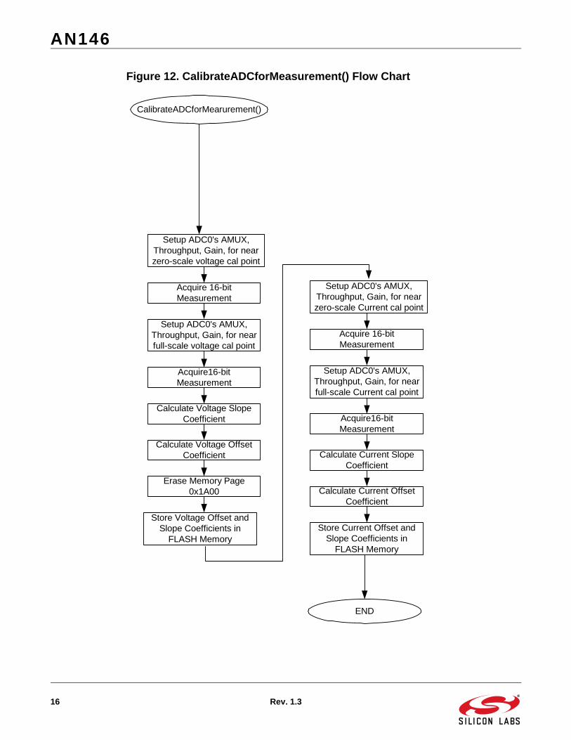
CalibrationTo ensure accurate voltage and current measure-ments, the algorithms use a two-point system cali-bration scheme. In this scheme, the user is expectedto apply two known voltages and two known cur-rents, preferable, one point near ground and theother point near full-scale. The algorithm then
takes these two points, calculates a slope and anoffset for both the current and voltage channels,and stores the results in FLASH. All future conver-sions are scaled relative to these slope and offsetcalculations.
TemperatureTo monitor the temperature, the algorithms use theon-chip temperature sensor. The sensor is leftuncalibrated, but still provides a sufficiently accu-rate temperature measurement. For more accuratetemperature measurement, one or two-point tem-perature calibration is required.
An external temperature sensor can be used ifdesired. The AMUX can be reconfigured to accom-modate this additional input voltage.
CurrentThe current delivered to the battery cells is moni-tored by measuring the voltage across a sense resis-tor (typically tens of mohms; our example uses a0.24 ohm resistor). To maximize current measure-ment accuracy, this reference design uses an exter-nal amplifier with a gain of 10. This provides about11-bits of current measurement accuracy (8-bitsfrom the ADC and 3-bits from the external gainamplifier). To further maximize current measure-ment accuracy, the raw current measurements arescaled via the slope and offset calibration coeffi-cients every time a measurement conversion istaken.
To determine the minimum current resolution,recall that the output code of a ADC is given byEquation 3
DoutAin 2n
Vref--------------------=
Equation 3. Digital Output Code.

AN146
Rev. 1.3 7
Accounting for the external amplifier, Equation 4
states that Ain is
Iin is then given by Equation 5
Assuming
• Rs = 0.24 • VREF = 3.3 V
• 2N = 256, an 8-bit converter• External Gain = 10• No External Gain = 1
When Dout = 1, IMIN is given by Equation 6.
When Dout=256, Imax is given by Equation 7.
It is important to note that if one chooses to modifythe algorithm, the order of mathematical operationsis important. To minimize truncation error effects,be sure to perform multiply operations first makingthe numerator as large as possible, before perform-ing divide operations. Further recall that a longtype variable, which is the limit for the F300’s
compiler, is limited to 232-1 or approximately 4 bil-lion.
VoltageThe battery’s voltages are divided down and moni-tored via external resistors. Note that this exampleuses the supply voltage as the ADC voltage refer-ence. Any monitored voltage above the referencevoltage must be divided down for accurate moni-toring. If a more accurate reference is required, anexternal voltage reference can be used. Adjustmentto the divide resistors must be made accordingly.
Charging - Phase1In Phase 1, (for description purposes, we assumethe battery is initially discharged), the ‘F30x regu-lates the battery’s current to ILOWCURRENT (typi-cally 1/50 C) until the battery’s voltage reachesVMINVOLTBULK. Note that the battery’s charge cur-rent is current limited to ILOWCURRENT to ensuresafe initial charge and to minimize battery self-heating. If at any time the temperature increases outof limit, charging is halted.
Charging - Phase 2Once the battery reaches VMINVOLTBULK the char-ger enters Phase 2, where the battery’s algorithmcontrols the PWM pass switch to ensure the outputvoltage provides a constant charge-current IBULKto the battery (rate or bulk current is usually 1C andis definable in the header file as is ILOWCURRENTand VMINVOLTBULK).
Charging - Phase 3After the battery reaches VTop (typically 4.2 V insingle cell charger), the charger algorithm entersPhase 3, where the PWM feeds back and regulatesthe battery’s voltage. In Phase 3, the battery contin-ues to charge until the battery’s charge currentreaches IMINIBULK, after which, the battery ischarged for an additional 30 minutes and thencharge terminates. Phase 3 typically takes themajority of the charging time.
Ain Iin Rs 10 =
Equation 4. Input Current with 10x Gain.
IinDout Vref
2n
10 Rs------------------------------------=
Equation 5. Input Current.
Imin 5.37 mACode---------------=
Equation 6. IMIN.
Imax 1.37 Amps=
Equation 7. Imax.

AN146
8 Rev. 1.3
Note that in most practical applications, such as aportable PC, the batteries may be in any of the threephases when charging is activated. This doesn’treally affect the charger as it simply monitors thebattery’s current condition and starts charging fromthat point.
Getting StartedThe reference design that accompanies this appli-cation note is designed to charge a single cell 4.2 Vlithium ion battery. To accommodate numerouspower supplies and batteries, it charges at 250mAbulk current. To charge a battery, first connectpower to the board by applying an 8V to 15V sup-ply to JP1. The power supply should be able to sup-ply a minimum of 500mA. Once the appropriatesupply is connected, connect the battery to JP3.Connect the positive lead of the battery to pin 1 andconnect the negative lead to pin 3. Terminal 2 ofJP3 can be left unconnected as no code has beendeveloped to monitor temperature via an externaltemperature sensor at this time. Finally, press thereset switch and the battery will begin charging.The PWM charge control signal can be monitoredby probing pin 5 on the C8051F300.
Recommended Operating Conditions
• Supply: 8V to 15V• Battery: One cell, 4.2V,
with <1000mAh ratingDefault Charging Parameters
• Trickle Current = 135mA• Bulk Current = 250mA• Regulation Voltage = 4.2V• Termination Current = 125mAEfficiency of Charger
• Switching Efficiency > 80%• Voltage Accuracy > 1%• Current Accuracy > 2%
Charging 2 Cells or More
To charge more than 1 battery cell, both the hard-ware and software will need to be modified. Forexample, to charge two 4.2 V batteries simultane-ously, resistors R11 and R12 will need to beswitched. Then, the header file will need thesemodifications:
CELLs = 2
RESB = 10
Once the header file is modified, recompile thesoftware and down load the new source code to thecharger board. A similar scheme can be used tomodify the board for any number of cells.
ConclusionThe C8051F300’s high level of analog integration,small form-factor, integrated FLASH memory, andlow power consumption make it ideal for flexiblenext generation battery charging applications. Thisnote discussed how to use the C8051F300 in Lith-ium Ion battery charger applications at 510kHzswitch rate. Example code is provided as well.
ReferenceApplications of Linear Integrated Circuits.Eugene Hnatek, John Wiley and Sons, 1975.

AN146
Rev. 1.3 9
Appendix A - SchematicFigure 5. High Speed Charger Schematic.

AN146
10 Rev. 1.3
Appendix B - Bill Of MaterialsFigure 6. High Speed Charger Bill of Materials.
Ite
mQ
TY
Pa
rtV
alu
eP
ack
ag
eN
ote
s
11
U1
C80
51F
300
ML
P-1
1C
ygn
al
Inte
gra
ted
Pro
du
cts
C80
51F
300
21
U3
LP
V32
1M5
SO
T-2
3-5
Na
tio
na
l (L
PV
321M
5 o
r e
qu
iva
len
t)3
1Q
1N
-Ch
an
ne
lS
OT
-23
Zete
x,
N-C
ha
nn
el
30-V
(D
-S)
MO
SF
ET
, (2
N70
02C
T o
r e
qu
iva
len
t)4
1Q
2P
-Ch
an
ne
lS
OT
-23
Zete
x,
P-C
ha
nn
el
30-V
(D
-S)
MO
SF
ET
, (Z
XM
P3A
13F
CT
-ND
or
eq
uiv
ale
nt)
51
L1
22u
HS
MD
Co
il C
raft
In
du
cto
r, 2
2uH
, 1.
5 A
, (D
O33
16P
-223
or
eq
uiv
ale
nt)
62
D3,
4S
cho
ttky
SM
C3A
40V
Po
we
r R
ect
ifie
r D
iod
e (
MB
RS
340C
T o
r e
qu
iva
len
t)7
6C
3,5,
7,9,
10,1
20.
1uF
0805
Ca
p X
7R 5
0V 5
% (
Ke
me
t C
0805
C10
4J5R
AC
TU
or
eq
uiv
ale
nt)
81
C4
33p
F08
05C
ap
X7R
, 50
V 1
0% (
Ke
me
t C
0805
330J
5GA
CT
U o
r e
qu
iva
len
t)9
1C
61
uF
0805
Ca
p X
7R,
10V
10%
(K
em
et
C08
0510
5K8R
AC
TU
or
eq
uiv
ale
nt)
101
C8
22u
FE
IA60
32-2
8C
ap
Ta
nta
lum
, 16
V,
10%
(K
em
et
T49
1C22
6K01
6AS
or
eq
uiv
ale
nt)
111
C11
100p
F08
05C
ap
X7R
50V
5%
(K
em
et
C08
05C
101K
5GA
CT
U o
r e
qu
iva
len
t)12
2R
3,15
100k
0805
Re
sist
or
1/10
W,
5% (
Pa
na
son
ic P
100K
CC
T-N
D o
r e
qu
iva
len
t)13
5R
4,10
,11,
13,1
410
k08
05R
esi
sto
r 1/
10W
, 5%
(P
an
aso
nic
P10
.0K
CC
T-N
D o
r e
qu
iva
len
t)14
1R
91k
0805
Re
sist
or
1/10
W,
5% (
Pa
na
son
ic P
1.0K
CC
T-N
D o
r e
qu
iva
len
t)15
2R
8,16
200
0805
Re
sist
or
1/10
W,
5% (
Pa
na
son
ic P
200C
CT
-ND
or
eq
uiv
ale
nt)
161
R12
20k
0805
Re
sist
or
1/10
W,
5% (
Pa
na
son
ic P
20.0
KC
CT
-ND
or
eq
uiv
ale
nt)
171
S1
Sw
itch
6MM
, S
QM
om
en
tary
sw
itch
(P
an
aso
nic
P80
07S
-ND
or
eq
uiv
ale
nt)
181
RS
EN
SE
0.24
oh
m08
05R
esi
sto
r 1/
4W,
2% (
Pa
na
son
ic R
L12
T0.
24G
CT
or
eq
uiv
ale
nt)
BO
M T
OT
AL
Incl
ud
ed
on
De
mo
Bo
ard
, b
ut
NO
T P
art
of
Ba
tte
ry C
ha
rge
r B
OM
Ite
mQ
TY
Pa
rtV
alu
eP
ack
ag
eN
ote
s
11
U2
MIC
5235
SO
T-2
3-5
Mic
rel
Se
mic
on
du
cto
r (M
IC52
35-3
.3M
5)2
1C
11
uF
0805
Ca
p X
7R,
10V
10%
(K
em
et
C08
0510
5K8R
AC
TU
or
eq
uiv
ale
nt)
31
C2
2.2
uF
EIA
3216
-18
Ca
p T
an
talu
m,
16V
, 10
% (
Ke
me
t T
491A
225K
016A
S o
r e
qu
iva
len
t)4
2R
1,R
247
5 o
hm
0805
Re
sist
or
1/10
W,
5% (
Pa
na
son
ic P
475C
CT
-ND
or
eq
uiv
ale
nt)
52
R5,
71k
0805
Re
sist
or
1/10
W,
5% (
Pa
na
son
ic P
1.0K
CC
T-N
D o
r e
qu
iva
len
t)6
1R
610
k08
05R
esi
sto
r 1/
10W
, 5%
(P
an
aso
nic
P10
.0K
CC
T-N
D o
r e
qu
iva
len
t)7
1D
1L
ED
, R
ed
0.1"
th
ru h
ole
T-1
3/4
(P
an
aso
nic
LN
21R
PH
L o
r e
qu
iva
len
t)8
1D
2L
ED
, G
ree
n0.
1" t
hru
ho
leT
-1 3
/4 (
Pa
na
son
ic L
N31
GP
HL
or
eq
uiv
ale
nt)
91
Sh
un
tS
hu
nt
0.1"
Sh
un
t (9
2995
7-08
or
eq
uiv
ale
nt)
102
JP1,
JP2
1x2
He
ad
er
0.1"
th
ru h
ole
Su
llin
s (S
2105
-02
or
eq
uiv
ale
nt)
111
JP3
1x3
He
ad
er
0.1"
th
ru h
ole
Su
llin
s (S
2105
-03
or
eq
uiv
ale
nt)
121
JP4
2x5
He
ad
er
0.1"
th
ru h
ole
Pro
tect
ed
wit
h c
en
tra
l p
ola
rizi
ng
ke
y sl
ot
(3M
251
0-60
02U
B o
r e
qu
iv.)
131
P1
RA
PC
722
2x5.
5mm
Ja
ckS
wit
chcr
aft
(S
C11
53-N
D o
r e
qu
iva
len
t)14
1B
oa
rd2-
La
yer
2"x
1.75
"P
CB
EX
PR
ES
S (
bo
ard
ma
nu
fact
uri
ng
se
rvic
es)

AN146
Rev. 1.3 11
Appendix C - PCB Layout Figure 7. High Speed Charger Layout (Silk Screen)
Buck Regulator Sub-circuit
JP3: Battery Input
Battery(+)TempBattery(-)
JP1: 8V-15V Input Supply Terminal
(+)(-)
3.3V LDO & Power LED
Reset Switch
C2 Interface
Current and Voltage Feedback Monitoring Sub-circuits
C8051F300
Terminal
AN146
12 Rev. 1.3
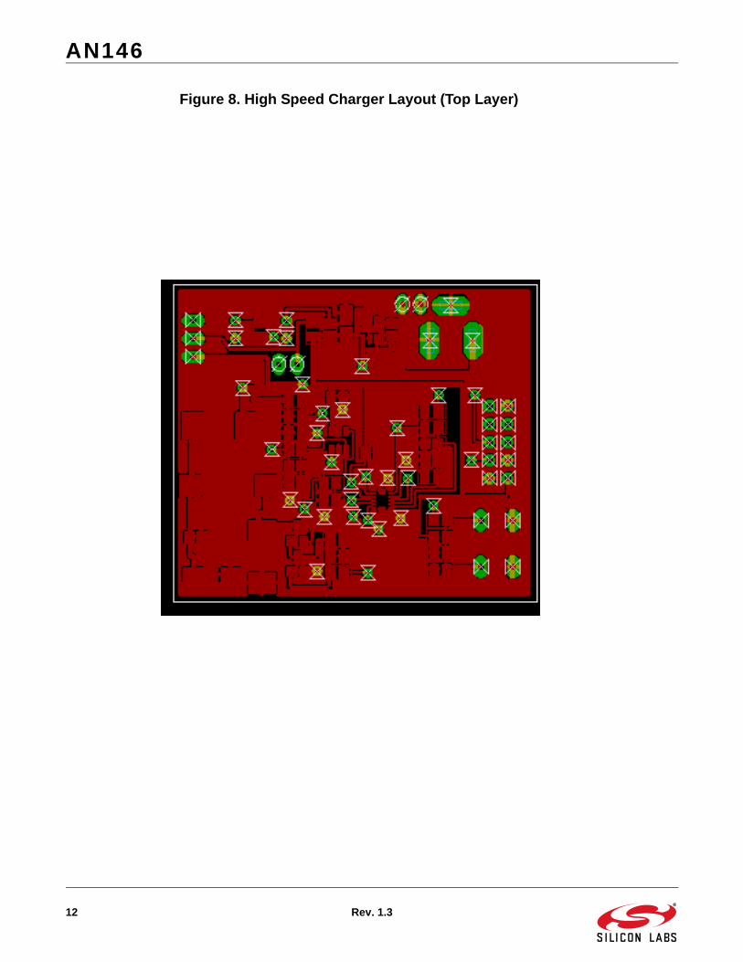
Figure 8. High Speed Charger Layout (Top Layer)

AN146
Rev. 1.3 13
Figure 9. High Speed Charger Layout (Bottom Layer)

AN146
14 Rev. 1.3
Figure 10. High Speed Charger Bill of Materials
Item
QT
YP
art
Val
ue
Pac
kag
eN
ote
sp
()
11
U1
C8
051
F30
0M
LP
-11
Cyg
na
l In
teg
rate
d P
rod
uct
s C
805
1F
300
21
U3
LP
V32
1M5
SO
T-2
3-5
Nat
ion
al (
LP
V32
1M5
or
equ
ival
ent)
31
Q1
N-C
han
ne
lS
OT
-23
Ze
tex
, N-C
ha
nn
el 3
0-V
(D
-S)
MO
SF
ET
, (2
N70
02C
T o
r eq
uiv
ale
nt)
41
Q2
P-C
ha
nn
el
SO
T-2
3Z
ete
x, P
-Ch
ann
el 3
0-V
(D
-S)
MO
SF
ET
, (Z
XM
P3A
13F
CT
-ND
or
eq
uiv
alen
t)5
1L
12
2uH
SM
DC
oil
Cra
ft In
du
cto
r, 2
2u
H, 1
.5 A
, (D
O3
316
P-2
23 o
r e
qu
iva
len
t)6
2D
3,4
Sch
ott
kyS
MC
3A
40V
Po
wer
Re
cti
fier
Dio
de
(M
BR
S3
40C
T o
r eq
uiv
ale
nt)
76
C3,
5,7,
9,10
,12
0.1u
F08
05C
ap X
7R 5
0V 5
% (
Kem
et C
0805
C10
4J5R
AC
TU
or
equ
ival
ent)
81
C4
33p
F08
05C
ap X
7R, 5
0V 1
0% (
Kem
et C
0805
330J
5GA
CT
U o
r eq
uiv
alen
t)9
1C
61
uF
0805
Cap
X7R
, 10V
10%
(K
emet
C08
0510
5K8R
AC
TU
or
equ
ival
ent)
101
C8
22u
FE
IA60
32-2
8C
ap T
anta
lum
, 16V
, 10%
(K
emet
T49
1C22
6K01
6AS
or
equ
ival
ent)
111
C11
100p
F08
05C
ap X
7R 5
0V 5
% (
Kem
et C
0805
C10
1K5G
AC
TU
or
equ
ival
ent)
122
R3,
1510
0k08
05R
esis
tor
1/10
W, 5
% (
Pan
aso
nic
P10
0KC
CT
-ND
or
equ
ival
ent)
135
R4,
10,1
1,13
,14
10k
0805
Res
isto
r 1/
10W
, 5%
(P
anas
on
ic P
10.0
KC
CT
-ND
or
equ
ival
ent)
141
R9
1k08
05R
esis
tor
1/10
W, 5
% (
Pan
aso
nic
P1.
0KC
CT
-ND
or
equ
ival
ent)
152
R8,
1620
008
05R
esis
tor
1/10
W, 5
% (
Pan
aso
nic
P20
0CC
T-N
D o
r eq
uiv
alen
t)16
1R
1220
k08
05R
esis
tor
1/10
W, 5
% (
Pan
aso
nic
P20
.0K
CC
T-N
D o
r eq
uiv
alen
t)17
1S
1S
wit
ch6M
M, S
QM
om
enta
ry s
wit
ch (
Pan
aso
nic
P80
07S
-ND
or
equ
ival
ent)
181
RS
EN
SE
0.24
oh
m08
05R
esis
tor
1/4W
, 2%
(P
anas
on
ic R
L12
T0.
24G
CT
or
equ
ival
ent)
Incl
ud
ed o
n D
em
o B
oa
rd, b
ut
NO
T P
art
of
Bat
tery
Ch
arg
er
BO
MIt
emQ
TY
Par
tV
alu
eP
acka
ge
No
tes
p(
)1
1U
2M
IC52
35S
OT
-23-
5M
icre
l Sem
ico
nd
uct
or
(MIC
5235
-3.3
M5)
21
C1
1 u
F08
05C
ap X
7R, 1
0V 1
0% (
Kem
et C
0805
105K
8RA
CT
U o
r eq
uiv
alen
t)3
1C
22.
2 u
FE
IA32
16-1
8C
ap T
anta
lum
, 16V
, 10
% (
Kem
et T
491A
225K
016A
S o
r eq
uiv
alen
t)4
2R
1,R
247
5 o
hm
080
5R
esi
sto
r 1/
10W
, 5%
(P
an
aso
nic
P4
75C
CT
-ND
or
equ
ival
ent)
52
R5,
71k
0805
Res
isto
r 1/
10W
, 5%
(P
anas
on
ic P
1.0K
CC
T-N
D o
r eq
uiv
alen
t)6
1R
610
k08
05R
esis
tor
1/10
W, 5
% (
Pan
aso
nic
P10
.0K
CC
T-N
D o
r eq
uiv
alen
t)7
1D
1L
ED
, Re
d0.
1" t
hru
ho
leT
-1 3
/4 (
Pan
as
on
ic L
N2
1RP
HL
or
eq
uiv
ale
nt)
81
D2
LE
D, G
reen
0.1"
th
ru h
ole
T-1
3/4
(P
ana
so
nic
LN
31G
PH
L o
r e
qu
ival
ent)
91
Sh
un
tS
hu
nt
0.1
"S
hu
nt
(92
995
7-0
8 o
r e
qu
ival
ent)
102
JP1,
JP2
1x2
Hea
der
0.1"
th
ru h
ole
Su
llin
s (S
2105
-02
or
equ
ival
ent)
111
JP3
1x3
Hea
der
0.1"
th
ru h
ole
Su
llin
s (S
2105
-03
or
equ
ival
ent)
121
JP4
2x5
Hea
der
0.1"
th
ru h
ole
Pro
tect
ed w
ith
cen
tral
po
lari
zin
g k
ey s
lot
(3M
251
0-60
02U
B o
r eq
uiv
.)13
1P
1R
AP
C72
22x
5.5m
m J
ack
Sw
itch
craf
t (S
C11
53-N
D o
r eq
uiv
alen
t)1
41
Bo
ard
2-L
aye
r2"
x1
.75"
PC
BE
XP
RE
SS
(b
oar
d m
an
ufa
ctu
rin
g s
erv
ices
)

AN146
Rev. 1.3 15
main()
Config_F300()
ErrorDetected
?
BULK_charge()
Turn off LED0, Error
No
CalibrateADCforMeasurement()
Enable Interrupts
Clear Termination FlagsClear Charge Status Flags
Yes
LOWCURRENT_charge()
No
Status = BULK?
Status =LOWCURRENT
?
ErrorDetected
?
Infinite Loop
Yes/No
Yes
No
Yes
Turn on LED0
InfiniteLoop
Yes/No
Figure 11. main() Flow Chart
AN146
16 Rev. 1.3
CalibrateADCforMearurement()
END
Setup ADC0's AMUX,Throughput, Gain, for nearzero-scale voltage cal point
Acquire 16-bitMeasurement
Setup ADC0's AMUX,Throughput, Gain, for nearfull-scale voltage cal point
Calculate Voltage SlopeCoefficient
Calculate Voltage OffsetCoefficient
Erase Memory Page0x1A00
Store Voltage Offset andSlope Coefficients in
FLASH Memory
Acquire16-bitMeasurement
Setup ADC0's AMUX,Throughput, Gain, for nearzero-scale Current cal point
Acquire 16-bitMeasurement
Setup ADC0's AMUX,Throughput, Gain, for nearfull-scale Current cal point
Calculate Current SlopeCoefficient
Calculate Current OffsetCoefficient
Store Current Offset andSlope Coefficients in
FLASH Memory
Acquire16-bitMeasurement
Figure 12. CalibrateADCforMeasurement() Flow Chart

AN146
Rev. 1.3 17
Appendix D - Software Flow Charts
Monitor_Battery()
MeasurementType
?
AMUX = Current AMUX = Volt
AV = AV + ADC0 Turn PWM on
Stop PWM
I?
ADC0 Done?
AMUX = Volt
Stop PWM
AMUX = Temperature
Start ADC0
AV = AV/10
END
No
Current Charge Voltage Temperature Battery Voltage
AV = 0I = 0
Yes
No
Yes
Calculate Voltage w/Calibration Coefficients
Calculate Current w/Calibration Coefficients
Calculate Temperature w/Calibration Coefficients
TemperatureCurrentVoltage w/ or w/out PWM
Return Desired Parameter
Figure 13. Monitor_Battery() Flow Chart

AN146
18 Rev. 1.3
Bulk_Charge()
Start PWM w/ Zero Output
TWithin Limits
?
Yes
Status = const_C
Calculate bulk_finish_time
Green LED On
Regulate Battery Current
Read Charge Voltage
Change Status fromconst_C to const_V
V<max_V &> min_Bulk
?
Status =BULK & No
Error?
Status =const_c
?
ChargeVoltage Within
Limits?
Yes
No
No
ACB D
Yes
No
No
No
Yes
Yes
Set Appropriate Flags
Figure 14. Bulk_Charge() Flow Chart (Part 1)

AN146
Rev. 1.3 19
Status =const_V &
Currentwithin Limits
?
Yes
Regulate Voltage()
Stop PWM& Flag Error
Stop PWM& Flag Error
Status = const_CStatus = LOWCURRENT
Green LED Off
TimeOverflow
?
Temp.Overflow
?
60 Sec.Over
?
DelayTimeOver
?
Yes
No
No
ACB D
Yes
No
No
Yes
END
Stop PWM
const_V, NOT Delay & Current
Below Threshold?
Calculate bulk_finish_time
Status = Delay
No
No
Yes
Yes
Reset Flags for LowCurrent Constant
Current Mode
Figure 15. BULKCurrent() Flow Chart (Part 2)

AN146
20 Rev. 1.3
LOWCURRENT_charge()
ResetTimeBase()
Tempwithin Limits
?
ChargeVoltage
Within Limits?
V<max_V
?
Green LED Blinking
Status = const_V
Regulate Voltage
LowcurrentFinish Timereached?
Stop PWMand flag error
Change Statusfrom const_C to
const_V
Status = Delay
Green LED Off
END
No
Yes
No
Yes
Yes
Yes
Yes
No
No
Yes
Calculate Finish_time
No ERROR &LOWCURRENT =1
?
No
Regulate Current
V<BulkThreshold
?
Prepare Flags to enterBulk Mode
No
Yes
No
Figure 16. LowCurrent_Charge() Flow Chart

AN146
Rev. 1.3 21
Turn_PWM_Off()
END
Increment CEX1Counter
CEX1Counter<0xF0?
CEX1Counter<0xF0?
No
Yes
No
Disable PWM Mode
Yes
Figure 17. Turn_PWM_Off() Flow Chart

AN146
22 Rev. 1.3
measure()
END
i = 0?
Set accumulator andcounter i variables to zero
Yes
accumulator =accumulator + ADC0
Increment i
Clear End of ConversionFlag
ConversionComplete
?
No
Return 16-bitMeasurement
No
Start New Conversion
Yes
Figure 18. Measure() Flow Chart

AN146
Rev. 1.3 23
Make Duty Cycle Larger
Voltage <VOLT_BULK &PCA not max
?
END
Measure Battery'svoltage
Voltage >VOLT_BULK &
PCA not 0
Make Duty Cycle Smaller
Regulate_Voltage()
Voltage< VOLT_BULK + Tolerence
& > VOLT_BULK?
No
Yes
Yes
Yes
No
No
Figure 19. Regulate_Voltage() Flow Chart

AN146
24 Rev. 1.3
Make Duty Cycle Larger
Current <passed current &
PCA not max?
END
Current >passed current &
PCA not 0
Make Duty Cycle Smaller
Regulate_Current()
No
Yes
Yes
Yes
No
No
Measure Current
Monitor Voltagew/ PWM off
Current =passed value
?
Voltage < VOLT_LOWCURRENT
± Tolerence?
CHARGE_STATUS =const_V
No
Yes
Figure 20. Regulate_Current() Flow Chart

AN146
Rev. 1.3 25
PCA_OVERFLOW_ISR()
END
60 = time.sec?
Yes
Increment time.hour
Reset time.hour
Reset time.count tooverflow value
0 = time.count
No
No
24 = time.hour
LOWCURRENTcharge &no errors
?
oddsecond
?
Reset PCA Counter andPCA Interrupts
Yes
Increment time.min
60 = time.min?
Yes
Reset time.min
Reset time.sec
Increment time.sec
No
Yes
No
No
No
Yes
Yes
Turn on LED
Turn Off LED
Decrement time.count
Figure 21. PCA_OVERFLOW_ISR() Flow Chart

AN146
26 Rev. 1.3
Appendix E - Firmware (Header File)//-----------------------------------------------------------------------------//// Copyright 2003 Cygnal Integrated Products, Inc.// // Filename: F300_HighSpeed_BC.h// Target Device: 8051F300// Created: 1 MAR 2003// Created By: DKC// Tool chain: KEIL Eval C51//// This header file is used to define all preprocessor directives, prototypes, // and global variable for F300_HighSpeed_BC.c.//// The user should modify this header file before proceeding as key // battery parameter limits are set here.//
//-----------------------------------------------------------------------------// Function Prototypes//-----------------------------------------------------------------------------void Config_F300(void);void Reset_Time_Base(void);void CalibrateADCforMeasurement(void);void Regulate_Current(int);void Regulate_Voltage(void);void Turn_PWM_Off(void);int Monitor_Battery(unsigned char);void Bulk_Charge(void);void Lowcurrent_Charge(void);unsigned int Measure(void);
//-----------------------------------------------------------------------------// UNIONs, STRUCTUREs, and ENUMs//-----------------------------------------------------------------------------typedef union LONG { // byte-addressable LONG long l; unsigned char b[4];} LONG;
typedef union INT { // byte-addressable INT int i; unsigned char b[2];} INT;
typedef struct{ unsigned long int t_count; int sec; // global seconds int min; // global minutes int hour; // global hour}time_struct;
//-----------------------------------------------------------------------------// Global Variable Definitions//-----------------------------------------------------------------------------time_struct TIME; // Global Struct to Track Time

AN146
Rev. 1.3 27
char bdata TERMINATION; // Global Variable to Track Termination char bdata CHARGE_STATUS; // Global Variable to Track Charging INT code CHECK_BYTE _at_ 0x1A00; // 0x0A0A Default value, for later useLONG code VOLT_SLOPE _at_ 0x1A60; // Volt Slope RegisterLONG code VOLT_OFFSET _at_ 0x1A64; // Volt Offset RegisterLONG code I_NOAMP_SLOPE _at_ 0x1A70; // Current Slope Register,ext. amp offLONG code I_NOAMP_OFFSET _at_ 0x1A74; // Current Offset Register,ext. amp.offLONG temp_LONG_1,temp_LONG_2; // Temporary Storage VariablesINT temp_INT_1,temp_INT_2; // Temporary Storage Variablesint Current = 0; // Most recent Current Measurementint Voltage = 0; // used to account for voltage drop // across sense resistor
//-----------------------------------------------------------------------------// Bit maskable CHARGE STATUS Register Definition//-----------------------------------------------------------------------------sbit BULK = CHARGE_STATUS^0; // bit 0 : BULK charge status bitsbit LOWCURRENT = CHARGE_STATUS^1; // bit 1 : LOWCURRENT charge status bitsbit ERROR = CHARGE_STATUS^2; // bit 2 : ERROR before/during chargingsbit CONST_V = CHARGE_STATUS^3; // bit 3 : charged w/ constant VOLTAGEsbit CONST_C = CHARGE_STATUS^4; // bit 4 : charged w/ constant CURRENTsbit DELAY = CHARGE_STATUS^5; // bit 5 : BULK charge DELAY for LiIon // after CURRENT threshold detectionsbit READY = CHARGE_STATUS^6; // bit 6 : Lowcurrent charge is // terminated; battery is chargedsbit FREE1 = CHARGE_STATUS^7; // bit 7 : Not Currently used
//-----------------------------------------------------------------------------// Bit Maskable TERMINATION Register Definition//-----------------------------------------------------------------------------sbit TEMP_MIN = TERMINATION^0; // bit 0 : minimum TEMPERATURE overflowsbit TEMP_MAX = TERMINATION^1; // bit 1 : maximum TEMPERATURE overflowsbit I_MIN = TERMINATION^2; // bit 2 : minimum CURRENT overflowsbit I_MAX = TERMINATION^3; // bit 3 : maximum CURRENT overflowsbit TIME_MAX = TERMINATION^4; // bit 4 : maximum time overflowsbit VOLT_MAX = TERMINATION^5; // bit 5 : maximum VOLTAGE overflowsbit VOLT_MIN = TERMINATION^6; // bit 6 : minimum VOLTAGE overflowsbit FREE2 = TERMINATION^7; // bit 7 : Not Currently used
//-----------------------------------------------------------------------------// Bit maskable PORT Definitions//-----------------------------------------------------------------------------sbit LED0 = P0 ^ 2; // bit 2 : LED0, Pin P0.2sbit CMPOUT = P0 ^ 3; // bit 3 : Comparator Outputsbit CMPIN1 = P0 ^ 4; // bit 4 : Comparator + Inputsbit CMPIN2 = P0 ^ 5; // bit 5 : Comparator - Inputsbit CEX0 = P0 ^ 6; // bit 6 : Frequency Output Mode.sbit CEX1 = P0 ^ 7; // bit 7 : 8-bit PWM // AMUX Selections; Analog Inputs#define VBAT 0xF0; // bit 0 : Voltage Ch.; Analog In#define IBAT 0xF1; // bit 1 : Current Ch.; Analog In#define TBAT 0xF8; // bit 2 : Temp. Ch.; Analog In
//-----------------------------------------------------------------------------// 8051F300 PARAMETERS//-----------------------------------------------------------------------------#define SYSCLK 24500000 // System clock frequency#define TEMP_SENSOR_GAIN 3300 // Temp Sensor Gain in (uV / degC)#define TEMP_GAIN 2 // PGA gain setting

AN146
28 Rev. 1.3
#define INT_CURRENT_GAIN 1 // PGA gain setting#define EXT_CURRENT_GAIN 10 // External gain setting#define VREF 3300 // ADC Voltage Reference (mV)#define SCRATCH_PAGE 0x1C00 // FLASH page used for temp storage#define PWM_CLOCK SYSCLK/255 // PWM frequency is 96 kHz
//-----------------------------------------------------------------------------// Calibration/Calculation PARAMETERS//-----------------------------------------------------------------------------#define V1_CAL 67 // 1st cal point for 2 point cal.#define V2_CAL 2800 // 2nd cal point for 2 point cal.#define I1_CAL 33 // 1st cal point for 2 point cal.#define I2_CAL 2800 // 2nd cal point for 2 point cal.#define RSENSE 24 // RSENSE is default to 240mohm#define RESB 20 // 20k Ohms,Voltage Divide Resistor#define RESAB 30 // 30k Ohms,Sum of Divide Resistor
#define TEMP_SLOPE ((long) TEMP_GAIN * TEMP_SENSOR_GAIN * 65536 / 100 / VREF) // An estimate of the Temperature<SLOPE> // in [tenth codes / K] // The temperature measurement is // within 3 degrees of accuracy.
//-----------------------------------------------------------------------------// Monitor_Battery Switch PARAMETERS//-----------------------------------------------------------------------------#define TEMPERATURE 7 // Value for Switch Statement#define VOLTAGE 5 // Value for Switch Statement#define VOLTAGE_PWM_OFF 3 // Value for Switch Statement#define CURRENT 1 // Value for Switch Statement
//-----------------------------------------------------------------------------// Battery/Pack Parameters//-----------------------------------------------------------------------------#define CELLS 1 // Number of cells in the battery pack#define CAPACITY 250 // mAh, Battery Capacity (LiIon)#define LiIon_CELL_VOLT 4200 // mV, Nominal Charge Voltage#define I_BULK (unsigned int)(CAPACITY)#define I_LOWCURRENT (unsigned int)(135)#define VOLT_BULK (unsigned int)(CELLS*LiIon_CELL_VOLT)
#define VOLT_LOWCURRENT (unsigned int)(CELLS*LiIon_CELL_VOLT)
#define VOLT_TOLERANCE (unsigned int)(CELLS*LiIon_CELL_VOLT/100)// 1 Percent Acc#define CURRENT_TOLERENCE (unsigned int)(CAPACITY/10) // 10 Percent Acc #define IMIN 100 // Minium Battery Charging is 100 mA#define IMAX 1350 // Maximum Allowed Current to Protect Hardware
//-----------------------------------------------------------------------------// Battery Characteristics: Charge TERMINATION Limits//-----------------------------------------------------------------------------#define MIN_TEMP_ABS 26300 // Abs. min. TEMPERATURE = -10 C, 263K #define MAX_TEMP_ABS 35300 // Abs. max. TEMPERATURE = 70C, 323K:#define MIN_VOLT_BULK (unsigned int)(CELLS*LiIon_CELL_VOLT*2/3) // Minimum BULK Voltage #define MAX_VOLT_ABS (unsigned int)(CELLS * LiIon_CELL_VOLT)#define MIN_I_BULK (unsigned int)(125)#define MAX_TIME_LOWCURRENT 30 // Max Lowcurrent Charge Time = 90min #define MAX_TIME_BULK 90 // Maximum BULK Charge Time = 90 min

AN146
Rev. 1.3 29
// at 1C CURRENT#define BULK_TIME_DELAY 30 // DELAY = 30min after “MIN_I_BULK”END OF FILE

AN146
30 Rev. 1.3
Appendix F - Firmware (Source File)
//-----------------------------------------------------------------------------//// Copyright 2003 Cygnal Integrated Products, Inc.// // Filename: F300_HighSpeed_BC.c// Target Device: 8051F300// Created: 1 March 2003// Created By: DKC// Tool chain: KEIL Eval C51//// This is a stand alone battery charger for a Lithium ION battery.// It utilizes a buck converter, controlled by the on-chip 8-bit PWM,// to provide constant current followed by constant voltage battery charge.// The High Frequency Output Mode is used to generate the switch rate. // The default rate is 510 kHz.////-----------------------------------------------------------------------------// Includes//-----------------------------------------------------------------------------#include <c8051f300.h>#include “F300_HighSpeed_BC.h” // Battery Hearder File //-----------------------------------------------------------------------------// Functions//-----------------------------------------------------------------------------
void Config_F300(void){ RSTSRC = 0x02; // Enable VDD Monitor XBR0 = 0x37; // Skip P0.0,1,2,4,5; they’re analog In XBR1 = 0x90; // Enable P0.6, P0.7, as CEX0 and CEX1 XBR2 = 0x40; // Make CEX0 an 8-Bit PWM // and CEX1 Frequency Output Mode // Also, Enable crossbar and weak pull-ups
CMPIN2 = 1; // Make Comparator Output Initially low CMPIN1 = 0; // to minimize current spikes on start-up
P0MDOUT = 0xC8; // Set P0.3,6,7 output to push-pull P0MDIN = 0xC8; // Configure P0.0,1,2,4,5 as Analog Inputs
OSCICN = 0x07; // Set SYSCLK to 24.5MHz, internal osc.
ADC0CN = 0xC0; // Turn on the ADC Module; // enable low power mode for settling
REF0CN = 0x0C; // Configure ADC’s to use VDD for // Voltage Reference, // Enable On-chip Temperature Sensor
//----------------------------------------------------------------// Comparator Register Configuration//----------------------------------------------------------------
CPT0MX = 0x22; // Comparator 0 MUX Selection Register // P0.4,5 Input to Comparator

AN146
Rev. 1.3 31
// P0.3 Output of Comparator CPT0MD = 0x00; // Comparator 0 Mode Selection Register CPT0CN = 0x80; // Comparator 0 Control Register, Turn on //-----------------------------------------------------------------------------// PCA Configuration//----------------------------------------------------------------------------- PCA0MD = 0x00; // Disable WDT PCA0MD = 0x08; // Set PWM Time base = SYSCLK
PCA0L = 0x00; // Initialize PCA Counter to Zero PCA0H = 0x00;
PCA0CN = 0x40; // Enable PCA Counter // Clear PCA Counter Overflow flag //Module 0 PCA0CPM0 = 0x00; // Configure CCM0 to Frequency Output Mode PCA0CPL0 = 0x28; // Initialize PCA PWM to small duty cycle PCA0CPH0 = 0x28; // 0x18 makes output frequency ~510kHz // 0x28 makes output frequency ~306kHz //Module 1 PCA0CPM1 = 0x42; // Configure CCM0 to 8-bit PWM mode PCA0CPL1 = 0xE0; // Initialize PCA PWM to small duty cycle PCA0CPH1 = 0xE0; // 0xB9 Ensures a Soft Initial Charge
//Module 2 PCA0CPM2 = 0x49; // Configure Module 1 as software timer PCA0CPL2 = 0xFF; // Initialize to 255 so that Interrupt // is generated when PCA ends // 8-bit PWM Cycle PCA0CPH2 = 0x00; // PCA0CPH is the high byte of the // Output Compare Module
EIE1 = 0x08; // Enable PCA Overflow Interrupt}
//-----------------------------------------------------------------------------// Reset_Time_Base - Resets all Time Counting Values//-----------------------------------------------------------------------------void Reset_Time_Base(){ TIME.sec = 0x00; TIME.min = 0x00; TIME.hour = 0x00; TIME.t_count = PWM_CLOCK; }
//-----------------------------------------------------------------------------// Initialize CalibrateADCforVoltageMeasurement//-----------------------------------------------------------------------------// This function calibrates the voltage channel and stores the calibration// coefficients in the parameters volt_slope and volt_offset.//void CalibrateADCforMeasurement()// This calibration routine uses a 2 point cal. { unsigned char xdata *pwrite; // FLASH write pointer long i=0;

AN146
32 Rev. 1.3
EA = 0; // Disable All Interrupts
// Wait until 1st calibration voltage is ready for cal //while (SW0 == 1); // Wait until SW0 pushed for (i=0;i<100000;i++); // Wait for Switch Bounce // Once ready, Get the first calibration voltage AMX0SL = VBAT; // Select appropriate input for AMUX ADC0CF = (SYSCLK/5000000) << 3; // ADC conversion clock = 5.0MHz ADC0CF &=0xF8; // Clear any Previous Gain Settings ADC0CF |= 0x01; // PGA gain = 1 temp_INT_1.i = Measure();
// Wait until 2nd calibration voltage is ready for cal //while (SW0 == 1); // Wait until SW0 pushed //for (i=0;i<100000;i++); // Wait for Switch Bounce
// Once ready, Get the 2nd calibration voltage AMX0SL = VBAT; //Change Mux for second point temp_INT_2.i = Measure(); // Calculate the SLOPE // V1 and V2 are in tenth of a degree temp_LONG_1.l = (unsigned)(temp_INT_2.i-temp_INT_1.i); temp_LONG_1.l *= (unsigned)100; // Account for Math Truncation Error temp_LONG_1.l /= (unsigned)(V2_CAL - V1_CAL);
// Calculate the OFFSET temp_LONG_2.l = (unsigned)temp_INT_1.i; temp_LONG_2.l -= (signed)(temp_LONG_1.l * V1_CAL/100); temp_LONG_1.l = 2050; // If no cal. use these temp_LONG_2.l = 0; // as default values // Erased memory at page 0x1A00 pwrite = (char xdata *)&(CHECK_BYTE.b[0]);
PSCTL = 0x03; // MOVX writes target FLASH memory; // FLASH erase operations enabled
FLKEY = 0xA5; // FLASH key sequence #1 FLKEY = 0xF1; // FLASH key sequence #2 *pwrite = 0x00; // initiate PAGE erase
// Write the Volt SLOPE and OFFSET to Flash PSCTL = 1; // MOVX writes to Flash pwrite = (char xdata *)&(VOLT_SLOPE.b[0]); FLKEY = 0xA5; FLKEY = 0xF1; // enable flash write *pwrite = temp_LONG_1.b[0]; pwrite = (char xdata *)&(VOLT_SLOPE.b[1]); FLKEY = 0xA5; FLKEY = 0xF1; // enable flash write *pwrite = temp_LONG_1.b[1]; pwrite = (char xdata *)&(VOLT_SLOPE.b[2]); FLKEY = 0xA5; FLKEY = 0xF1; // enable flash write *pwrite = temp_LONG_1.b[2];
AN146
Rev. 1.3 33
pwrite = (char xdata *)&(VOLT_SLOPE.b[3]); FLKEY = 0xA5; FLKEY = 0xF1; // enable flash write *pwrite = temp_LONG_1.b[3];
pwrite = (char xdata *)&(VOLT_OFFSET.b[0]); FLKEY = 0xA5; FLKEY = 0xF1; // enable flash write *pwrite = temp_LONG_2.b[0]; pwrite = (char xdata *)&(VOLT_OFFSET.b[1]); FLKEY = 0xA5; FLKEY = 0xF1; // enable flash write *pwrite = temp_LONG_2.b[1]; pwrite = (char xdata *)&(VOLT_OFFSET.b[2]); FLKEY = 0xA5; FLKEY = 0xF1; // enable flash write *pwrite = temp_LONG_2.b[2]; pwrite = (char xdata *)&(VOLT_OFFSET.b[3]); FLKEY = 0xA5; FLKEY = 0xF1; // enable flash write *pwrite = temp_LONG_2.b[3]; PSCTL = 0; // MOVX writes target XRAM
//-----------------------------------------------------------------------------// Initialize CalibrateADCforCurrentMeasurement_NOAMP//-----------------------------------------------------------------------------// This function calibrates the current channel with no external amp// and stores the calibration coefficients in the // parameters i_noamp_slope and i_noamp__offset.//// This calibration routine uses a 2 point cal. // Wait until calibration voltage is ready for cal //while (SW0 == 1); // Wait until SW0 pushed //for (i=0;i<100000;i++); // Wait for Switch Bounce
// Once ready, Get the first calibration voltage AMX0SL = IBAT; // Select appropriate input for AMUX ADC0CF = (SYSCLK/5000000) << 3; // ADC conversion clock = 5.0MHz ADC0CF &=0xF8; // Clear any Previous Gain Settings ADC0CF |= 0x03; // Set PGA gain = 4 temp_INT_1.i = Measure(); // Acquire 16-bit Conversion temp_INT_1.i *= 2; // Account for Differential Mode // Wait until 2nd calibration voltage is ready for cal //while (SW0 == 1); // Wait until SW0 pushed //for (i=0;i<100000;i++); // Wait for Switch Bounce
// Once ready, Get the 2nd calibration voltage temp_INT_2.i = Measure(); // Acquire 16-bit Conversion temp_INT_2.i *=2; // Account for Differential Mode // Calculate the SLOPE temp_LONG_1.l = (unsigned)(temp_INT_2.i - temp_INT_1.i); temp_LONG_1.l *= (unsigned)100; // Account for Math Truncation Error temp_LONG_1.l /= (unsigned)(I2_CAL - I1_CAL); temp_LONG_1.l /= (unsigned)INT_CURRENT_GAIN;// Account for Gain
// Calculate the OFFSET

AN146
34 Rev. 1.3
temp_LONG_2.l = (signed)(temp_INT_1.i/INT_CURRENT_GAIN); temp_LONG_2.l -= (signed)(temp_LONG_1.l * V1_CAL/100); temp_LONG_1.l = 2050; // If no cal. use these temp_LONG_2.l = 0; // as default values
// Memory at 0x1A00 is already erased // Write the Volt SLOPE and OFFSET to Flash PSCTL = 1; // MOVX writes to Flash pwrite = (char xdata *)&(I_NOAMP_SLOPE.b[0]); FLKEY = 0xA5; FLKEY = 0xF1; // enable flash write *pwrite = temp_LONG_1.b[0]; pwrite = (char xdata *)&(I_NOAMP_SLOPE.b[1]); FLKEY = 0xA5; FLKEY = 0xF1; // enable flash write *pwrite = temp_LONG_1.b[1]; pwrite = (char xdata *)&(I_NOAMP_SLOPE.b[2]); FLKEY = 0xA5; FLKEY = 0xF1; // enable flash write *pwrite = temp_LONG_1.b[2]; pwrite = (char xdata *)&(I_NOAMP_SLOPE.b[3]); FLKEY = 0xA5; FLKEY = 0xF1; // enable flash write *pwrite = temp_LONG_1.b[3];
pwrite = (char xdata *)&(I_NOAMP_OFFSET.b[0]); FLKEY = 0xA5; FLKEY = 0xF1; // enable flash write *pwrite = temp_LONG_2.b[0]; pwrite = (char xdata *)&(I_NOAMP_OFFSET.b[1]); FLKEY = 0xA5; FLKEY = 0xF1; // enable flash write *pwrite = temp_LONG_2.b[1]; pwrite = (char xdata *)&(I_NOAMP_OFFSET.b[2]); FLKEY = 0xA5; FLKEY = 0xF1; // enable flash write *pwrite = temp_LONG_2.b[2]; pwrite = (char xdata *)&(I_NOAMP_OFFSET.b[3]); FLKEY = 0xA5; FLKEY = 0xF1; // enable flash write *pwrite = temp_LONG_2.b[3]; PSCTL = 0; // MOVX writes target XRAM}
//-----------------------------------------------------------------------------// Measure//-----------------------------------------------------------------------------//// This routine averages 65536 ADC samples and returns a 16-bit unsigned // result.// unsigned int Measure (void){ unsigned i; // sample counter unsigned long accumulator=0L; // here’s where we integrate the // ADC samples

AN146
Rev. 1.3 35
// read the ADC value and add to running total i = 0; do { AD0INT = 0; // clear end-of-conversion indicator AD0BUSY = 1; // initiate conversion while(!AD0INT); // wait for conversion to complete accumulator += ADC0; // read adc value and accumulate i++; // update counter } while (i != 0x0000); // the accumulator now contains 16 added bits of which 8 are usable return (unsigned int) (accumulator >> 8); }
//-----------------------------------------------------------------------------// Regulate_Current//-----------------------------------------------------------------------------// This routine monitors the battery’s current and adjusts // the PWM (i.e. duty cycle) to keep the current at a known value//void Regulate_Current(int passed_current){ unsigned int temp = 0,delay_count = 0; do{ temp = Monitor_Battery(CURRENT); // Measure Current if (temp < passed_current) { PCA0CPH1--;
for(delay_count = 0;delay_count<2500;delay_count++);}
if (temp > passed_current) { PCA0CPH1++; for(delay_count = 0;delay_count<2500;delay_count++); } }while ((temp < (passed_current - CURRENT_TOLERENCE)) || (temp > (passed_current + CURRENT_TOLERENCE))); // I_BULK or I_LOWCURRENT is set now
temp = Monitor_Battery(VOLTAGE_PWM_OFF); // If VOLTAGE within range, // change from constant CURRENT charge // mode to constant VOLTAGE charge mode if ((temp >= (VOLT_LOWCURRENT - VOLT_TOLERANCE*2)) && (temp <= (VOLT_LOWCURRENT + VOLT_TOLERANCE*2))) { CONST_C = 0; CONST_V = 1; }
}
//-----------------------------------------------------------------------------// Regulate_Voltage//-----------------------------------------------------------------------------// This routine monitors the battery’s voltage and adjusts // the PWM (i.e. duty cycle) to keep the voltage at a known value//void Regulate_Voltage(void){ unsigned int temp = 0,delay_count = 0;

AN146
36 Rev. 1.3
// set VOLT_BULK (with “soft start”) do{ temp = Monitor_Battery(VOLTAGE);
if (temp < VOLT_BULK) { PCA0CPH1--; for(delay_count = 0;delay_count<2500;delay_count++); } if (temp > VOLT_BULK) { PCA0CPH1++; for(delay_count = 0;delay_count<2500;delay_count++); }
}while ((temp < (VOLT_BULK - VOLT_TOLERANCE)) || (temp > (VOLT_BULK + VOLT_TOLERANCE))); // VOLTAGE is set now}
//-----------------------------------------------------------------------------// Turn_PWM_Off//-----------------------------------------------------------------------------// This routine peforms a soft charge turn off by taking the PWM’s // duty cycle slowly to zero.//void Turn_PWM_Off(void){ do{ if (PCA0CPH1 < 0xF0) PCA0CPH1++; }while (PCA0CPH1 < 0xF0); // Duty Cycle is now small and safe to turn off.
PCA0CPM0 = 0x00; // Disable PWM}
//-----------------------------------------------------------------------------// Monitor_Battery//-----------------------------------------------------------------------------// This routine acts as a switch when gathering different conversion types.// It adjusts the throughput, adjust the AMUX and returns the current in mA,// voltage in mV, and temperature in C, 2% accurate.//int Monitor_Battery(unsigned char value){ char i; unsigned long av =0,delay_count=0; long signed result;
ADC0CF = (SYSCLK/5000000) << 3; // ADC conversion clock = 5.0MHz ADC0CF &= 0xF8; // Clear any Previous Gain Settings switch (value) { case TEMPERATURE: //Turn_PWM_Off(); // Turn PWM Off AMX0SL = TBAT; // Select appropriate input for AMUX ADC0CF |= 0x02; // Set PGA gain = 2 break;

AN146
Rev. 1.3 37
case VOLTAGE: AMX0SL = VBAT; // Select appropriate input for AMUX ADC0CF |= 0x01; // Set PGA gain = 1 break;
case VOLTAGE_PWM_OFF: //Turn_PWM_Off(); // Turn PWM Off AMX0SL = VBAT; // Select appropriate input for AMUX ADC0CF |= 0x01; // Set PGA gain = 1 break;
case CURRENT: AMX0SL = IBAT; // Select appropriate input for AMUX ADC0CF |= 0x01; // Set PGA gain = 1 break;
} //Compute average of next 10 A/D conversions for(delay_count = 0;delay_count<2500;delay_count++);// Allow Settling Time for(av=0,i=10;i;--i){ AD0INT = 0; // clear end-of-conversion indicator AD0BUSY = 1; // initiate conversion while(!AD0INT); // wait for conversion to complete av = av+ADC0; }
av = av/10; // Compute the average av = av<<8; // Convert to 16-bit conversion // ...to account for 16-bit cal. // coefficients PCA0CPM0 = 0x46; // Turn on PWM
switch (value) { case TEMPERATURE: result = (long) av * 1000/TEMP_SLOPE; break;
case VOLTAGE: case VOLTAGE_PWM_OFF: result = (av - VOLT_OFFSET.l); // Account for System Errors result *= 100; // Account for Math Truncation Error result *= RESAB; // Account for Divide Resistors
result /= VOLT_SLOPE.l; // Convert to Voltage in Millivolts result /= RESB; result -= ((RSENSE*Current)/100); // Account for Sense Resistor Voltage Drop
break; case CURRENT: result = (av - I_NOAMP_OFFSET.l); // Account for System Errors result *= 100; // Account for Math Truncation Error result *= 100; // Account for Sense Resistor
result /= I_NOAMP_SLOPE.l; // Convert to Milliamps result /= RSENSE; // Account for Sense Resistor result /= EXT_CURRENT_GAIN; // Account for external Amplifier
Current = (int) result; break;
}

AN146
38 Rev. 1.3
return (int) result; }
//-----------------------------------------------------------------------------// Bulk_Charge Function//-----------------------------------------------------------------------------void Bulk_Charge(void){ unsigned int temp = 0; unsigned int bulk_finish_hour = 0; unsigned int bulk_finish_min = 0; unsigned int delay_hour = 0; unsigned int delay_min = 0; unsigned int last_min = 0; Reset_Time_Base(); // Reset Time Base to zero
// Calculate BULK charge finish time bulk_finish_min = (TIME.min + MAX_TIME_BULK); bulk_finish_hour = TIME.hour; while (bulk_finish_min > 60) { bulk_finish_min = bulk_finish_min - 60; bulk_finish_hour++; }
CONST_C = 1; // Start in constant current charge mode DELAY = 0; // Reset timer DELAY
temp = Monitor_Battery(TEMPERATURE); // Monitor Temperature // Is temperature within range? if ((temp > MIN_TEMP_ABS) && (temp < MAX_TEMP_ABS)) { temp = Monitor_Battery(VOLTAGE); // Monitor Voltage
// Is Voltage within range? Voltage = temp; // for Debug
if ((temp <= (MAX_VOLT_ABS + VOLT_TOLERANCE)) && (temp > MIN_VOLT_BULK)) { PCA0CPM0 = 0x46; // Turn on PWM
// Enter main loop in Bulk_Charge() while ((BULK == 1) && (ERROR == 0)) { if (CONST_C == 1) Regulate_Current(I_BULK);
else if (CONST_V == 1) { Current = Monitor_Battery(CURRENT); // Measure Current if((Current < IMIN)||(Current > IMAX)) { CONST_V = 0; // Exit CONST_V CONST_C = 1; // Prepare to enter CONST_C BULK = 0; // Prepare to exit BULK mode LOWCURRENT = 1; // Prepare to enter LOWCURRENT Mode
if (Current < IMIN) I_MIN = 1; // Indicate Specific Error for Debug

AN146
Rev. 1.3 39
else I_MAX = 1; // Indicate Specific Error for Debug }
else if ((Current < IMAX) && (Current > IMIN)) { I_MAX = 0; // Reset Error Flag
I_MIN = 0; // Reset Error Flag Regulate_Voltage(); // Charge with Constant Voltage } }
// Now, Check for error and charge termination conditions // If above max charge time, flag error // Test for BULK Charge Time Out // Monitor Time if ((TIME.hour == bulk_finish_hour) && (TIME.min == bulk_finish_min) && (DELAY == 0)) { Turn_PWM_Off(); // Turn Off PWM TIME_MAX = 1; // Set Time max error flag ERROR = 1; // Set general error flag }
// Monitor Temperature temp = Monitor_Battery(TEMPERATURE); if ((temp < MIN_TEMP_ABS) && (temp > MAX_TEMP_ABS))
{ Turn_PWM_Off(); // Turn Off PWM
if (temp < MIN_TEMP_ABS) TEMP_MIN = 1; // Set Temperature below minimum flag else TEMP_MAX = 1; // Set Temperature exceeds maximum flag ERROR = 1; // Set general error flag } // Minute elapsed? // Check for minimum current // if reached, enter last DELAY charge if (TIME.min != last_min) { last_min = TIME.min; if ((CONST_V == 1) && (DELAY == 0) && (Monitor_Battery(CURRENT) <= MIN_I_BULK)) { // Calculate TOP OFF Battery Time finish time delay_min = (TIME.min + BULK_TIME_DELAY); delay_hour = TIME.hour; while (delay_min > 60) { delay_min = delay_min - 60; delay_hour++; } DELAY = 1; // Set Delay Flag } // Monitor Delay time, time up?

AN146
40 Rev. 1.3
if ((TIME.hour == delay_hour)&&(TIME.min == delay_min) && (DELAY == 1)) { Turn_PWM_Off(); // Turn Off PWM CONST_V = 0; // Exit CONST_V CONST_C = 1; // Prepare to enter CONST_C BULK = 0; // Prepare to exit BULK mode LOWCURRENT = 1; // Prepare to enter LOWCURRENT Mode } } } // End Main While loop } else if(ERROR == 0) { if (temp > (MAX_VOLT_ABS + VOLT_TOLERANCE)) { VOLT_MAX = 1; // Set Max Voltage error flag ERROR = 1; // Set general error flag }
else if(temp < MIN_VOLT_BULK) { VOLT_MIN = 1; // Set Minimum bulk voltage error flag LOWCURRENT = 1; // Switch to LOWCURRENT mode BULK = 0; // Exit Bulk Charge mode } // battery’s voltage very low } }
else if(ERROR == 0) // Absolute temperature out of range? { if (temp < MIN_TEMP_ABS) TEMP_MIN = 1; // Set Temperature below minimum flag else TEMP_MAX = 1; // Set Temperature exceeds maximum flag ERROR = 1; // Set general error flag }}
//-----------------------------------------------------------------------------// Lowcurrent_Charge //-----------------------------------------------------------------------------
void Lowcurrent_Charge(void){ unsigned int temp = 0; unsigned int lowcurrent_finish_min = 0; unsigned int lowcurrent_finish_hour = 0;
Reset_Time_Base(); // Reset Time base to zero
// Calculate LOWCURRENT finish time lowcurrent_finish_min = (TIME.min + MAX_TIME_LOWCURRENT); lowcurrent_finish_hour = TIME.hour; while (lowcurrent_finish_min > 60) { lowcurrent_finish_min = lowcurrent_finish_min - 60; lowcurrent_finish_hour++; }

AN146
Rev. 1.3 41
// Enter Main Lowcurrent Loop. // Only exits are upon error and full charge while ((LOWCURRENT == 1) && (ERROR == 0)) { temp = Monitor_Battery(TEMPERATURE);// Get Temperature Reading // Is TEMPERATURE within limits if ((temp > MIN_TEMP_ABS) && (temp < MAX_TEMP_ABS)) { // Is Battery’s Charge Voltage below max charge voltage temp = Monitor_Battery(VOLTAGE); // Get Voltage Reading if (temp <= (VOLT_LOWCURRENT + VOLT_TOLERANCE)) { if (CONST_C == 1) // CONST_C ?, charge w/ constant current Regulate_Current(I_LOWCURRENT);
if (CONST_V == 1) // CONST_V?, charge w/ constant voltage Regulate_Voltage(); if ((temp >= MIN_VOLT_BULK) && (DELAY == 0))// Bulk Threshold voltage met? { LOWCURRENT = 0; // Exit LOWCURRENT mode BULK = 1; // Switch to Bulk Charge mode } // Check elapsed time if ((TIME.hour == lowcurrent_finish_hour) && ( TIME.min == lowcurrent_finish_min)) { TIME_MAX = 1; // Set Time MAX error flag ERROR = 1; // Set general error flag } } else if(ERROR == 0) // Voltage to high? { VOLT_MAX = 1; // Set Max voltage error flag ERROR = 1; // Set general error flag } } else if(ERROR == 0) // Absolute temperature out of range? { if (temp < MIN_TEMP_ABS) TEMP_MIN = 1; // Set Temperature below minimum flag else TEMP_MAX = 1; // Set Temperature exceeds maximum flag ERROR = 1; // Set general error flag } }}
//-----------------------------------------------------------------------------// Main Function//-----------------------------------------------------------------------------void main(void){ EA = 0; // Disable All Interrupts Reset_Time_Base(); Config_F300(); // Config F300//Turn_PWM_Off(); // Turn PWM off before Calibration//CalibrateADCforMeasurement(); // Calibrate F300

AN146
42 Rev. 1.3
EA = 1; // Enable All Active Interrupts
while(1) { LED0 = 0; // Turn LED0 off TERMINATION = 0x00; // Reset Termination Flags CHARGE_STATUS = 0x00; // Reset Charge Status Flags
LOWCURRENT = 0;BULK = 1; // Start in LOWCURRENT Charge Mode
CONST_C = 1;
while (ERROR == 0) { if (BULK == 1) { Bulk_Charge(); // Enter Bulk Charge Mode
} if (LOWCURRENT == 1) Lowcurrent_Charge(); // Enter Lowcurrent_Charge function // Toggle LED0 at 1 Hz rate via ISR }
if (ERROR == 1) { Turn_PWM_Off();; // Turn PWM Off EA = 0; // Disable All Interrupts while (1); // Enter a eternal loop // No recovery except “reset-button” } } }
//-----------------------------------------------------------------------------// Interrupt Service Routines//-----------------------------------------------------------------------------
//-----------------------------------------------------------------------------// PCA_ISR//-----------------------------------------------------------------------------// This routine counts the elapsed time in seconds, minutes, hours.// It also toggles LED0 every second when in Lowcurrent Charge Mode.// This routine interrupts every time the PCA counter overflows, every 256// SYSCLK cycles. After SYSCLK/256 interrupts, one second has elapsed.// void PCA_OVERFLOW_ISR (void) interrupt 9{ int time_sec; PCA0CN = 0x40; // Reset all PCA Interrupt Flags
PCA0H = 0x00; // Reset High Byte of PCA Counter // of 8-bit PWM we are using Module1
if (0x0000 == --TIME.t_count) { TIME.t_count = PWM_CLOCK; // Reset 1 Second Clock if ( 60 == ++TIME.sec ) // Account for elapsed seconds { // Reset second counter every minute TIME.sec = 0x00; if ( 60 == ++TIME.min ) // Account for elapsed minutes

AN146
Rev. 1.3 43
{ // Reset minute counter every hour TIME.min = 0x00; if ( 24 == ++TIME.hour ) // Account for elapsed hours TIME.hour = 0x00; // Reset hour counter every day } } time_sec = TIME.sec;
if ((LOWCURRENT == 1) && (ERROR == 0)) { // Blink LED0 at 1 Hz if in Lowcurrent //if (TIME.sec % 2) // LED0 = 0; // Turn on LED every odd second //else // LED0 = 1; // Turn on LED every even second } }}
END OF FILE

http://www.silabs.com
Silicon Laboratories Inc.400 West Cesar ChavezAustin, TX 78701USA
Simplicity Studio
One-click access to MCU and wireless tools, documentation, software, source code libraries & more. Available for Windows, Mac and Linux!
IoT Portfoliowww.silabs.com/IoT
SW/HWwww.silabs.com/simplicity
Qualitywww.silabs.com/quality
Support and Communitycommunity.silabs.com
DisclaimerSilicon Labs intends to provide customers with the latest, accurate, and in-depth documentation of all peripherals and modules available for system and software implementers using or intending to use the Silicon Labs products. Characterization data, available modules and peripherals, memory sizes and memory addresses refer to each specific device, and "Typical" parameters provided can and do vary in different applications. Application examples described herein are for illustrative purposes only. Silicon Labs reserves the right to make changes without further notice and limitation to product information, specifications, and descriptions herein, and does not give warranties as to the accuracy or completeness of the included information. Silicon Labs shall have no liability for the consequences of use of the information supplied herein. This document does not imply or express copyright licenses granted hereunder to design or fabricate any integrated circuits. The products are not designed or authorized to be used within any Life Support System without the specific written consent of Silicon Labs. A "Life Support System" is any product or system intended to support or sustain life and/or health, which, if it fails, can be reasonably expected to result in significant personal injury or death. Silicon Labs products are not designed or authorized for military applications. Silicon Labs products shall under no circumstances be used in weapons of mass destruction including (but not limited to) nuclear, biological or chemical weapons, or missiles capable of delivering such weapons.
Trademark InformationSilicon Laboratories Inc.® , Silicon Laboratories®, Silicon Labs®, SiLabs® and the Silicon Labs logo®, Bluegiga®, Bluegiga Logo®, Clockbuilder®, CMEMS®, DSPLL®, EFM®, EFM32®, EFR, Ember®, Energy Micro, Energy Micro logo and combinations thereof, "the world’s most energy friendly microcontrollers", Ember®, EZLink®, EZRadio®, EZRadioPRO®, Gecko®, ISOmodem®, Precision32®, ProSLIC®, Simplicity Studio®, SiPHY®, Telegesis, the Telegesis Logo®, USBXpress® and others are trademarks or registered trademarks of Silicon Labs. ARM, CORTEX, Cortex-M3 and THUMB are trademarks or registered trademarks of ARM Holdings. Keil is a registered trademark of ARM Limited. All other products or brand names mentioned herein are trademarks of their respective holders.