IEEE TRANSACTIONS ON INDUSTRIAL … · IEEE TRANSACTIONS ON INDUSTRIAL ELECTRONICS, VOL. 51, NO. 6,...
8
IEEE TRANSACTIONS ON INDUSTRIAL ELECTRONICS, VOL. 51, NO. 6, DECEMBER 2004 1305 Packaging and Integration Technologies for Future High-Frequency Power Supplies Seán Cian Ó Mathúna, Patrick Byrne, Gerald Duffy, Weimin Chen, Matthias Ludwig, Member, IEEE, Terence O’Donnell, Member, IEEE, Paul McCloskey, and Maeve Duffy, Member, IEEE Abstract—This paper reviews data from the International Tech- nology Roadmap for Semiconductors to establish where dc–dc converters are headed in the first decade of the new millennium. It focuses on the high performance computing (high current, fast response, high power density) and portable/handheld (low profile) sectors. Magnetics and power device packaging technologies needed to allow power supplies to move to operating frequencies in the 1–10 MHz region are discussed. It introduces the concept of magnetic components fully embedded (windings and core) in PCB and silicon offering low profile and low losses at high frequency. It also reviews developments in wirebond-free power packaging such as flip-chip assembly that offer low profile, reduced parasitics and increased thermal performance. Finally, consideration is given to the changes in the power electronics industry that may need to be addressed to enable these new technologies to play a strategic role. Index Terms—Integrated magnetics, power packaging, power supplies, reviews, semiconductor device packaging. NOMENCLATURE CSP Chip scale package. FEM Finite-element method. MEMS Microelectromechanical systems. NMRC National Mircoelectronics Research Centre. NUI National University of Ireland PCB Printed circuit board. SEM Scanning electron microscope. TCE Thermal coefficient of expansion. I. INTRODUCTION E XCERPTS from the International Technology Roadmap for Semiconductor predict that by 2007, high performance processors will be operating at 0.7 V and dissipating 190 W [1]. This will result in a total current of over 270 A being delivered to a silicon device of dimensions 17.6 mm on a side with oper- ating speeds of up to 7 GHz. As an aside, it is worth noting the equivalent data for 2016 are quoted as 0.4 V, 288 W, over 700 A, 17.6 mm, and 29 GHz. These specifications present a signifi- cant technical challenge to the power supply with much research ongoing into the development of high-efficiency, fast response voltage regulation modules that can be located as close as pos- sible to the processor. Manuscript received February 3, 2003; revised December 12, 2003. Abstract published on the Internet September 10, 2004. S. C. Ó Mathúna, P. Byrne, G. Duffy, W. Chen, M. Ludwig, T. O’Donnell, and P. McCloskey are with the National Mircoelectronics Research Centre, Uni- versity College, Cork, Ireland (e-mail: [email protected]). M. Duffy is with the National University of Ireland, Galway, Ireland. Digital Object Identifier 10.1109/TIE.2004.837904 At the low power end of the scale, we are interested in the handheld/portable sector where battery power, and, in the fu- ture, fuel cells, will require low cost, low profile, miniaturized dc–dc converters (incorporating power management functions) with both single and multivoltage outputs for a range of de- vices including low voltage processors, radio-frequency/wire- bond-free transceiver circuits, and high voltage displays. A number of recent studies have addressed the question of the technological requirements that these trends will have on the power supply of the future. Van Wyk and Lee stated that, while power switching and power switching network technology had reached a high level of maturity in the previous 25 years, there was now a need for research and innovation to be focussed on packaging, manufacturing, and electromagnetic component in- tegration with conductive, interconnection, and power device structures [2]. The Power Sources Manufacturers Association reiterated these views in their 2000 Power Technology Roadmap study and emphasized the increasing importance of a synergy between electromechanical packaging and circuit design in achieving improvements in product cost and reliability [3]. In a key paper in 2000 from the then Lucent Power Systems, Huljak et al. presented a concise roadmap of performance/tech- nology developments required in distributed/point-of-load dc–dc converters over the ten-year period 1998 to 2008. The study emphasized the strong need to reduce power converter size by increasing converter frequency up to 10 MHz by 2008 [4]. Of the five areas listed as needing significant technological developments, two, magnetics and packaging, are the subject of this paper. In this paper, the limitations of existing magnetics and power packaging technologies will be discussed and compared with the benefits of more advanced technologies to provide reduced losses for both high current and high switching frequency con- verters. The integration of magnetic devices, using novel PCB and silicon technologies with embedded windings and magnetic layers, capable of operating in the range 1 to 10 MHz, will be presented. Recent trends and associated benefits of wirebond- free power device assembly will also be introduced and some of the key research challenges discussed. Finally, consideration is given to the impact these new, and potentially strategic, enabling technologies may have on the power electronics industry. II. INTEGRATED MAGNETICS To meet the requirements of future power supplies, magnetic components have to decrease in footprint and profile. At the 0278-0046/04$20.00 © 2004 IEEE
Transcript of IEEE TRANSACTIONS ON INDUSTRIAL … · IEEE TRANSACTIONS ON INDUSTRIAL ELECTRONICS, VOL. 51, NO. 6,...

IEEE TRANSACTIONS ON INDUSTRIAL ELECTRONICS, VOL. 51, NO. 6, DECEMBER 2004 1305
Packaging and Integration Technologies for FutureHigh-Frequency Power Supplies
Seán Cian Ó Mathúna, Patrick Byrne, Gerald Duffy, Weimin Chen, Matthias Ludwig, Member, IEEE,Terence O’Donnell, Member, IEEE, Paul McCloskey, and Maeve Duffy, Member, IEEE
Abstract—This paper reviews data from the International Tech-nology Roadmap for Semiconductors to establish where dc–dcconverters are headed in the first decade of the new millennium.It focuses on the high performance computing (high current, fastresponse, high power density) and portable/handheld (low profile)sectors. Magnetics and power device packaging technologiesneeded to allow power supplies to move to operating frequenciesin the 1–10 MHz region are discussed. It introduces the concept ofmagnetic components fully embedded (windings and core) in PCBand silicon offering low profile and low losses at high frequency. Italso reviews developments in wirebond-free power packaging suchas flip-chip assembly that offer low profile, reduced parasitics andincreased thermal performance. Finally, consideration is given tothe changes in the power electronics industry that may need to beaddressed to enable these new technologies to play a strategic role.
Index Terms—Integrated magnetics, power packaging, powersupplies, reviews, semiconductor device packaging.
NOMENCLATURE
CSP Chip scale package.FEM Finite-element method.MEMS Microelectromechanical systems.NMRC National Mircoelectronics Research Centre.NUI National University of IrelandPCB Printed circuit board.SEM Scanning electron microscope.TCE Thermal coefficient of expansion.
I. INTRODUCTION
EXCERPTS from the International Technology Roadmapfor Semiconductor predict that by 2007, high performance
processors will be operating at 0.7 V and dissipating 190 W [1].This will result in a total current of over 270 A being deliveredto a silicon device of dimensions 17.6 mm on a side with oper-ating speeds of up to 7 GHz. As an aside, it is worth noting theequivalent data for 2016 are quoted as 0.4 V, 288 W, over 700A, 17.6 mm, and 29 GHz. These specifications present a signifi-cant technical challenge to the power supply with much researchongoing into the development of high-efficiency, fast responsevoltage regulation modules that can be located as close as pos-sible to the processor.
Manuscript received February 3, 2003; revised December 12, 2003. Abstractpublished on the Internet September 10, 2004.
S. C. Ó Mathúna, P. Byrne, G. Duffy, W. Chen, M. Ludwig, T. O’Donnell,and P. McCloskey are with the National Mircoelectronics Research Centre, Uni-versity College, Cork, Ireland (e-mail: [email protected]).
M. Duffy is with the National University of Ireland, Galway, Ireland.Digital Object Identifier 10.1109/TIE.2004.837904
At the low power end of the scale, we are interested in thehandheld/portable sector where battery power, and, in the fu-ture, fuel cells, will require low cost, low profile, miniaturizeddc–dc converters (incorporating power management functions)with both single and multivoltage outputs for a range of de-vices including low voltage processors, radio-frequency/wire-bond-free transceiver circuits, and high voltage displays.
A number of recent studies have addressed the question ofthe technological requirements that these trends will have on thepower supply of the future. Van Wyk and Lee stated that, whilepower switching and power switching network technology hadreached a high level of maturity in the previous 25 years, therewas now a need for research and innovation to be focussed onpackaging, manufacturing, and electromagnetic component in-tegration with conductive, interconnection, and power devicestructures [2].
The Power Sources Manufacturers Association reiteratedthese views in their 2000 Power Technology Roadmap studyand emphasized the increasing importance of a synergy betweenelectromechanical packaging and circuit design in achievingimprovements in product cost and reliability [3].
In a key paper in 2000 from the then Lucent Power Systems,Huljak et al. presented a concise roadmap of performance/tech-nology developments required in distributed/point-of-loaddc–dc converters over the ten-year period 1998 to 2008. Thestudy emphasized the strong need to reduce power convertersize by increasing converter frequency up to 10 MHz by 2008[4]. Of the five areas listed as needing significant technologicaldevelopments, two, magnetics and packaging, are the subjectof this paper.
In this paper, the limitations of existing magnetics and powerpackaging technologies will be discussed and compared withthe benefits of more advanced technologies to provide reducedlosses for both high current and high switching frequency con-verters. The integration of magnetic devices, using novel PCBand silicon technologies with embedded windings and magneticlayers, capable of operating in the range 1 to 10 MHz, will bepresented. Recent trends and associated benefits of wirebond-free power device assembly will also be introduced and some ofthe key research challenges discussed. Finally, consideration isgiven to the impact these new, and potentially strategic, enablingtechnologies may have on the power electronics industry.
II. INTEGRATED MAGNETICS
To meet the requirements of future power supplies, magneticcomponents have to decrease in footprint and profile. At the
0278-0046/04$20.00 © 2004 IEEE
1306 IEEE TRANSACTIONS ON INDUSTRIAL ELECTRONICS, VOL. 51, NO. 6, DECEMBER 2004
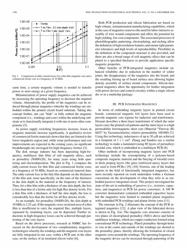
Fig. 1. Comparison of eddy-current losses for a thin film magnetic core and acommercial ferrite core at a frequency of 10 MHz.
same time, a certain magnetic volume is needed to transferpower or store energy at a given frequency.
Miniaturization of power supply magnetics can be achievedby increasing the operating frequency to decrease the requiredvolume. Alternatively, the profile of the magnetics can be re-duced through planar magnetics whereby the windings are em-bedded within the printed circuit board substrate. Taking thisconcept further, one can “hide” or fully embed the magneticcomponent (i.e., windings and core) within the underlying sub-strate or to functionally integrate it with one or more other com-ponents [5].
As power supply switching frequencies increase, losses inmagnetic materials increase significantly. A qualitative reviewof commercial ferrite materials shows that they are limited to thelower megahertz region and, while some performance and costimprovements are expected in the coming years, no significantbreakthroughs are envisaged for high-frequency ferrites [3].
The disk storage industry has been depositing high-fre-quency, multilayer, thin films of soft magnetic alloys, suchas permalloy (Ni80Fe20), for many years using both sput-tering and electrodeposition. The plot in Fig. 1 compares theeddy-current losses for thin film and commercial ferrite coresat a frequency of 10 MHz, based on commercial material data.The eddy-current loss in the thin film depends on the thicknessof the film and, more specifically, on the ratio of the thicknessto the skin depth in the material at the frequency of interest.Thus, for a thin film with a thickness of one skin depth, the lossis less than that of a ferrite only for high flux density levels. Fora thin film with a thickness of half the skin depth, the loss isconsiderably less than the ferrite for all flux density levels.
As an example, for permalloy (Ni80Fe20), the skin depth at10 MHz is 2.25 m. If the magnetic cross-sectional area of a thinfilm is insufficient to carry the required flux, multiple layers,separated by insulating layers, can be deposited. Further re-ductions in high-frequency losses can be achieved through pat-terning of the core layers.
Based on the above processes, research at NMRC has fo-cussed on the development of two complimentary magneticstechnologies whereby the windings and the magnetic core layersare fully integrated in one case, within a PCB and, in the othercase, on the surface of an insulated silicon wafer [6].
Both PCB production and silicon fabrication are based onhigh volume, semiautomated manufacturing capabilities, whichin the case of magnetics removes the need for labor-intensive as-sembly of wire wound components and offers the potential forhigh yielding, low cost components. The associated processes ofphotolithographic patterning, electroplating, and etching allowthe definition of high resolution features and ensure tight param-eter tolerances and high levels of reproducibility. Flexibility inthe definition of the component structure is also provided, andthere are also a broad range of soft magnetic alloys that can beplated to a specified thickness to provide application specificmagnetic properties.
Other benefits of PCB-integrated magnetics include en-hanced reliability due to reduction in the number of solderjoints; the disappearance of the magnetics into the board; andthe resulting freeing up of board surface area allowing higherdensity assembly of surface mount components. Silicon-inte-grated magnetics allow the opportunity for further integrationwith power devices and control circuitry within a single silicondie or in a multichip package.
III. PCB INTEGRATED MAGNETICS
In terms of embedding magnetic layers in printed circuitboards, commercial magnetic foil layers have been used toprovide magnetic core regions for inductors and transformers.Dezuari describes a three-layer transformer of which the outerlayers carry the printed coil patterns and the inner layer is a highpermeability ferromagnetic sheet core (Material “Vitrovac (R)6025” by Vacuumschmelze, relative permeability 100 000) [7].Using this technology, inductances of up to 30 H are achievedin a footprint of 1 1 cm . Zhang and Sanders use a similartechnology to make a laminated (using 80 layers of permalloy)toroidal core, which is embedded in a multilayer PCB [8].
Other methods of incorporating magnetic layers into PCBtechnology include the screenprinting of a polymer-basedcomposite magnetic material and the burying of toroidal coresin thick prepreg layers (the glass reinforced epoxy layers thatare used to form PCBs.) [9], [10]. Ferreira, one of the leadingexperts in the field of functionally integrated magnetics, hasmost recently reported on work undertaken within a Germanconsortium on the development of what they refer to as em-bedded passives integrated circuit. This project investigated thestate-of-the-art in embedding of passives (i.e., resistors, capac-itors, and magnetics) in PCB for power converters. A 100 Wconverter demonstrator contained embedded capacitive layersbut the magnetics were limited to standard planar magneticswith embedded PCB windings and planar ferrite cores [11].
The structure in Fig. 2 illustrates the concept of the PCB in-tegrated magnetics [12]. A plan view of the fabricated deviceis shown in Fig. 3(a). The magnetic core structure consists oftwo plates of electroplated permalloy (NiFe) above and belowmultilayer windings, which are copper conductors formed usingconventional PCB technology. Plated permalloy through-holesor vias at the center and outside of the windings are shorted tothe permalloy plates, thereby allowing the formation of closedmagnetic cores around the windings. The operating frequency ofthe magnetic device can be increased through patterning of the

Ó MATHÚNA et al.: PACKAGING AND INTEGRATION TECHNOLOGIES FOR FUTURE HIGH-FREQUENCY POWER SUPPLIES 1307
Fig. 2. Schematic of structure of PCB-integrated magnetics.
Fig. 3. (a) Plan view of PCB-integrated magnetic. (b) 1.5 W dc–dc converterassembled on embedded PCB integrated inductor.
permalloy plates, which reduces losses due to high-frequencyeddy currents within the highly conducting permalloy. Furtherimprovement is achieved through multilayer lamination of thepermalloy. For inductors carrying dc currents, PCB processingallows very controlled gaps to be introduced into the magneticplates.
A key advantage of the process is that it can be integratedseamlessly with traditional multilayer PCB manufacturingwithout significant cost implications.
Both inductors and transformers have been fabricated on aa dedicated pilot production line at NMRC. Fig. 3(b) showsa technology demonstrator of a 1.5 W, 3.3 V output, buckconverter, operating at 1 MHz, using a commercially availabledc–dc converter integrated circuit (IC) [13]. The converterincorporates a PCB integrated inductor of 4.7 H, with dccurrent handling capability up to 500 mA.
The footprint of the entire converter measures 10 mm 10mm with the discrete components assembled on top of the in-tegrated inductor to achieve an ultraflat and compact converterdesign. Efficiency measurements, taken at 1 MHz and plottedin Fig. 4, show a nearly constant efficiency over a wide rangeof load and measure approximately 70% efficiency for an inputvoltage of 7.22 V and 80% for 5 V input.
The technology also compares well, in terms of size and per-formance, with the discrete solution using an equivalent 1210sized surface mount inductor (3.2 mm 2.5 mm).
While further research is ongoing to enhance efficiencythrough reducing core losses and to develop a lower profileconverter with bare power and control die, results to date sug-gest that this technology offers a viable option for low profile,low cost converters in the portable/handheld sector for powerlevels in the range 1–10 W. Research is also ongoing to developFEMs, and ultimately, analytical models for optimization oflaminated and patterned magnetic core layers in PCB.
Fig. 4. Efficiency measurement against load current for a 4.7 mH,PCB-integrated inductor in a 1.5 W dc–dc converter.
Fig. 5. Silicon-integrated magnetics showing plated copper windings andplated permalloy core layer.
IV. SILICON INTEGRATED MAGNETICS
The silicon integrated magnetics concept is based on a combi-nation of traditional, thin film, semiconductor fabrication tech-nologies and state-of-the-art microsystems technologies. Fig. 5shows SEM images of the silicon magnetics being researchedat NMRC. The devices consist of electroplated copper coils, en-closed by an electroplated layer of soft magnetic material (i.e.,permalloy) [14], [15].
The feasibility of using thin-film magnetics for power con-version has been demonstrated [16]. Mino et al. demonstrated athin-film transformer integrated with Schottky diodes [17], andrecently Katayama et al. [18] demonstrated a 1 W dc–dc con-verter with a thin-film inductor integrated on an IC with powerswitches and control circuitry which achieved an overall powerdensity of 5.6 W/cm .
However, most of the thin-film magnetic components demon-strated to date have been restricted to low power conversion(typically 2 W), and power densities for such microtrans-formers are typically less than 1 W/cm . Sullivan et al. [19]did address the design of microtransformers for slightly higher

1308 IEEE TRANSACTIONS ON INDUSTRIAL ELECTRONICS, VOL. 51, NO. 6, DECEMBER 2004
Fig. 6. High aspect ratio plated copper windings.
powers (3 W) and predicted power densities of 59 W/cm .The use of microinductors for higher powers has also beenaddressed by Mehas et al. [20], specifically in the context ofrapid response, microprocessor power delivery.
To obtain high-efficiency, high-frequency transformers, thelosses in the windings and the core need to be minimized. Thelosses in the windings are directly related to the resistance of thecoils. By increasing the cross-sectional area of the coils usingthick electroplated copper, the winding resistance is reduced.The core losses are due mainly to eddy currents opposing themagnetizing flux. These eddy currents can be significantly re-duced using high resistivity and/or multilayer magnetic mate-rials, thereby also extending the frequency of operation of thedevices up to 10 MHz and beyond.
In the case of optimizing the power density, the footprint areaof the devices must be kept small. Therefore, using MEMS tech-nology (e.g., electrodeposition of copper into thick photoresistmold), high aspect ratio coils can be processed that ensure theconduction losses at high frequency can be minimized withoutincreasing the footprint as shown in Fig. 6.
Measured results from the most recent batch of fabricated mi-crotransformers yielded efficiencies of 50% for a power den-sity of 10 W/cm at 5 MHz. These devices were mainly usedto develop a predictive analytical model that would allow theoptimization of future designs. Fig. 7 shows a plot of both mea-sured and calculated open and short circuit inductance againstfrequency for the microtransformer. It can be seen that the de-vice, with a single layer of permalloy, operates up to 5 MHzwith the analytical model being accurate to within 20% of themeasured data. Using the validated model, it has been possibleto predict a performance of between 20 and 40 W/cm at ef-ficiencies up to 83% for devices incorporating two layers ofpermalloy. Fully optimized microtransformer structures are ex-pected to yield power densities as high as 50 W/cm at efficien-cies up to 95%.
These data suggest that microfabricated magnetics on sil-icon, as well as providing ultralow profile options for theportable/handheld electronics sector, may also provide a tech-nology compatible with future high performance processors.To achieve this goal will require thin-film materials with high
resistivity, low coercivity, high saturation magnetization, andthe capability of being deposited in multilayers.
V. POWER PACKAGING
As presented in the introduction, many recent studies haveidentified the limitations of traditional power device packaging(i.e., multiple, large diameter wire bonds attached to heat sinkleadframes) for future high density, high-efficiency, fast-re-sponse power supplies delivering hundreds of amps at outputvoltages below 1 V. When one considers that up to half theresistance (and most of the inductance) of a power MOSFETin a traditional package is attributed to the wire bonds andleadframe, it is clear that these specifications will be seriouslycompromised by the package-level parasitics.
One recognized route to achieving this optimized powerpackage design is to replace the conventional chip-to-board in-terconnect, wire bonding, with solder interconnections, givingwhat can be termed a “wirebond-free” interconnect scheme.
This technological shift has already been seen for low powerdevices with the packaging evolution from wirebond SO-8 andquad flat packages (QFPs) toward solder-bumped CSPs. (A chipscale package is one where the ratio of package to chip footprintis at a ratio between 1.0 and 1.2.) Wirebond-free CSPs for powerdevices refer to the concept of replacing wire bond connectionswith solder bump connections to the power semiconductor elec-trical contacts. This technology offers an attractive alternativebecause it has lower resistance and inductance levels, allowinghigher efficiency and higher switching frequency with the fur-ther advantage of a lower package profile. Furthermore, withoutthe restrictions of wirebonds on the active face of the power die,both sides of the die become available as thermal paths for im-proved heat dissipation.
Fig. 8 shows schematics of the various wirebond-freetechnologies, both for low power and very high power, re-cently introduced into commercial power switch products(IR, Fairchild, Flip Chip Technologies) or currently being re-searched (CPES, USA; NMRC, Ireland; INPG, France). Theseinclude a variant of the traditional power device large areasolder pads, the conventional, VLSI-inspired flip-chip bump,solder posts or stud bumps, stamped dimples on copper foil,and solder bars [21]–[28].
The following sections introduce what are seen as the keytechnical challenges in implementing these emerging assemblyprocesses.
A. Thermal Management
As power supplies are forced down a miniaturization routeand power densities increase, one can also expect increases inthermal management requirements. As mentioned above, a sig-nificant advantage of this CSP technology without wirebonds isthat, without the physical constraints of wire bonds, both facesof the die are available to provide low thermal resistance pathsfor improved heat dissipation from the power die. A numberof techniques are in use or have been proposed, which includea copper strap or lid soldered to the substrate, which providesan electrical connection for the MOSFET drain while also pro-viding an extra low thermal resistance path.

Ó MATHÚNA et al.: PACKAGING AND INTEGRATION TECHNOLOGIES FOR FUTURE HIGH-FREQUENCY POWER SUPPLIES 1309
Fig. 7. Measured and calculated open and short circuit inductance against frequency for silicon integrated microtransformer.
Fig. 8. Examples of wirebond-free power packaging technlogies for both low power discrete devices and high power modules.

1310 IEEE TRANSACTIONS ON INDUSTRIAL ELECTRONICS, VOL. 51, NO. 6, DECEMBER 2004
B. TCE Mismatch
While significant research data is available from VLSI flip-chip systems, the large-area solder bumps or pads needed forhigh current power devices mean that TCE mismatch issuesneed to be investigated separately to understand their impact onsolder joint lifetime.
The critical parameters that influence the fatigue lifetime ofthe solder joints are chip size, chip pad size, solder joint ge-ometry, underbump metallurgy (UBM) and thickness, substratematerial, and underfill. In terms of solder joint geometry forpower devices, large area solder bumps in an hourglass geom-etry with a large standoff have been shown to offer increasedlife times [27]. A polymer-based underfill can also significantlyincrease reliability by acting as a TCE matching buffer betweenthe power die and underlying substrate.
C. UBM
Because aluminum is not solderable, a pretreatment followedby the deposition of a solderable layer called a UBM is re-quired in advance of bump deposition. An increasingly popularaluminum pretreatment for chip bumping processes is a zincatetreatment that involves immersion of the aluminum-coatedsemiconductor substrate in an extremely low pH (i.e., highlycorrosive) sodium hydroxide-based solution containing zincions. This process step removes the native aluminum oxideand deposits a protective zinc layer. Upon immersion in anelectroless nickel plating solution, the zinc dissolves and isreplaced by nickel ions that initiate the autocatalytic depositionof the nickel UBM directly at the aluminum surface.
Research at NMRC has focused on the development of anovel, low cost activation and electroless UBM plating processthat reduces the number of processing steps while providinga less corrosive, more environmentally friendly processing ap-proach. Preliminary results have shown that this technology isreadily transferrable to power devices.
D. High Current Considerations
The phenomenon of electromigration has been the focus ofsignificant research in the microelectronics industry, where highcurrent densities now associated with submicrometer conductorlines can induce failures, in the form of voids and hillocks,which are also a function of temperature gradients and metalconductor grain size [29].
The impact of high currents in future power supplies is onlybeginning to attract attention where, by 2007, sub one volt, highperformance, microprocessor circuits are predicted to requiremore than 270 amps flowing into the load. The potential forassociated high current densities, and resulting electromigra-tion-induced failures at the power device, UBM, solder joint,and substrate level will require careful consideration in the con-text of developing high density power supply solutions with highlong-term reliability.
VI. CONCLUSION
This paper has introduced a number of packaging and integra-tion technologies that have the potential to address key issues inpower electronics circuits as a result of increasing switching fre-quencies, load currents, and power densities to meet the needs
of future high performance processors and low profile, low costportable/handheld electronics. The technologies described willreduce losses in both the magnetic components and the powerdevice assemblies as the converter switching frequencies movetoward 10 MHz, with currents reaching almost 300 A.
However, in order to reap the benefits of these technologies,the power electronics industry will need to consider how to im-plement the technologies in high volume to achieve low cost andhigh reliability.
The vast majority of power supply manufacturing facilities areset up for through-hole and surface mount assembly of passiveand active components, and sundry heat sinks, connectors, andenclosures. PCB and silicon integrated magnetics will requirethe establishment of external foundries with processes that arevariants of what currently is standard within the respective PCBand silicon manufacturing industries. PCB manufacturers willneed to enhance their capabilities in order to be able to manufac-ture and supply embedded magnetic components. In the case ofsilicon magnetics, dedicated foundries may become componentsuppliers.Furthermore,theconceptoffunctionalandsubstratein-tegration of magnetics presents a number of advantages that sug-gest these two technologies have the potential to play a key role inthe coming decade in providing a viable route to high-frequencymagnetics in a low profile, integrated construction.
On the power packaging side, the technologies described herewill introduce the need for familiarity with chip-scale pack-aging, flip-chip assembly where solder joints can no longer bevisually inspected, and handling, storage, and assembly of bareand/or semibare power die. Many companies may have to con-sider the subcontract route as a serious alternative to establishingnew, in-house facilities and capabilities.
The whole area of packaging and integration will becomea key enabler and differentiator in the development of futurepower converters. The packaging and integration technologiespresented here are mature technologies, established in the PCB,microelectronics, and hard magnetic disk industries. They havethe potential to become strategic technologies in the future ofthe power electronics industry.
ACKNOWLEDGMENT
The authors would like to acknowledge funding support fromEnterprise Ireland.
REFERENCES
[1] International Technology Roadmap for Semiconductors (2001). [On-line]. Available: http://public.itrs.net/Files/2001ITRS/Home.htm
[2] J. D. van Wyk and F. C. Lee, “Power electronics technology at the dawnof the new millenium – Status and future,” in Proc. IEEE PESC’99,Charleston, SC, 1999, pp. 3–12.
[3] PSMA Power Technology Roadmap (2000). [Online]. Available:www.psma.com
[4] R. J. Huljak et al., “Where are power supplied headed?,” in Proc. IEEEAPEC’00, Feb. 2000, pp. 10–17.
[5] A. Lotfi and J. Weld, “Integrated magnetic-semiconductor components,”in Proc. IEEE Int. Workshop Integrated Power Packaging, 1998, pp.39–43.
[6] M. Duffy et al., “Comparison of integrated magnetic component tech-nologies for power applications,” in Proc. Int. Power Electronics Conf.(IPEC), Tokyo, Japan, Apr. 2000, pp. 309–314.
[7] O. Dezuari, S. Gilbert, E. Belloy, and M. Gijs, “High inductance planartransformers,” in Proc. 2nd Eur. Conf. Magnetic Sensors and Actuators(EMSA’98), Sheffield, U.K., July 13–15, 1998, pp. 355–358.
[8] Y. Zhang and S. Sanders, “In-board magnetics processes,” in Proc. IEEEPESC’99, 1999, pp. 562–567.

Ó MATHÚNA et al.: PACKAGING AND INTEGRATION TECHNOLOGIES FOR FUTURE HIGH-FREQUENCY POWER SUPPLIES 1311
[9] J. Park and M. Allen, “Low temperature fabrication and characterizationof integrated packaging compatible ferrite core magnetic devices,” inProc. IEEE APEC’97, 1997, pp. 362–367.
[10] J. Trites and K. Krone, “Embedded ferromagnetic technology: Auto-mated high volume manufacturing of magnetic components,” in Proc.Int. Electronics Packaging Symp., 1996, pp. 203–212.
[11] W. Waffenschmidt and J. A. Ferreira, “Embedded passives intergratedcircuits for power converters,” in Proc. IEEE PESC’02., vol. 1, 2002,pp. 12–17.
[12] S. O’Reilly et al., “Magnetic components and their production,” U.S.Patent 6 150 915, Nov. 21, 2000.
[13] M. Ludwig et al., “PCB integrated inductors for low power DC/DC con-verter,” in Proc. IEEE APEC’02, vol. 1, Dallas, TX, 2002, pp. 319–325.
[14] M. Brunet, T. O’Donnell, J. O’Brien, P. McCloskey, and S. C. ÓMathuna, “Thick photoresist development for the fabrication of highaspect ratio magnetic coils,” J. Micromech. Microeng., vol. 12, no. 4,pp. 444–449, July 2002.
[15] M. Brunet et al., “Electrical performance of micro-transformers forDC-DC converter applications,” IEEE Trans. Magn., vol. 38, pp.3174–3176, Sept. 2002, to be published.
[16] S. Iyengar, T. M. Liakopoulos, and C. H. Ahn, “A DC/DC boost con-verter toward fully on-chip integration using new micromachined planarinductors,” in Proc. IEEE PESC’99, vol. 1, Charleston, SC, June 1999,pp. 72–76.
[17] M. Mino et al., “Planar microtransformer with monolithically-integratedrectifier diodes for micro-switching converters,” IEEE Trans. Magn.,vol. 32, pp. 291–296, Mar. 1996.
[18] Y. Katayama et al., “High power density MHz-switching monolithicDC-DC converter with thin film inductor,” in Proc. IEEE PESC’00,Galway, Ireland, June 2000, pp. 1485–1490.
[19] C. R. Sullivan and S. R. Sanders, “Design of microfabricated trans-formers and inductors for high-frequency power conversion,” IEEETrans. Power Electron., vol. 11, pp. 228–238, Mar. 1996.
[20] G. Mehas, K. D. Coonley, and C. R. Sullivan, “Converter and inductordesign for fast-response microprocesor power delivery,” in Proc. IEEEPESC’00, Galway, Ireland, June 18–23, 2000, pp. 1621–1626.
[21] D. G. Morrision, “Dual thermal paths double power handling for surfacemount MOSFETs’ power packaging and components,” Electron. Des.,pp. 33–36, Jan. 2002.
[22] Fairchild Technical Data Sheet [Online]. Available:http://www.fairchildsemi.com/
[23] T. Sammon, “WLP power components shrink portable equipment,” Adv.Packag., Feb. 2001.
[24] X. Liu and G.-Q. Lu, “D2BGA chip scale IGBT package,” in Proc. IEEEAPEC’01, 2001, pp. 1033–1039.
[25] S. S. Wen, D. Huff, and G. Q. Liu, “Dimple array interconnect techniquefor packaging power semiconductor devices and modules,” in Proc.ISPSD’01, 2001, pp. 69–74.
[26] C. Gillot, C. Schaeffer, C. Massit, and L. Meysene, “Double sidedcooling of high power IGBT modules using flip chip technology,” IEEETrans. Comp. Packag. Technol., vol. 24, pp. 698–704, Dec. 2001.
[27] S. Haque et al., “An innovative technique for packaging power elec-tronic building blocks using metal posts interconnected parallel platestructures,” IEEE Trans. Adv. Packag., vol. 22, pp. 136–144, May 1999.
[28] P. Elenius, H. Yang, and R. Benson, “Solder bars, a novel flip chip ap-plication for high power devices,” in Proc. IEEE Electronic ComponentsTechnology Conf., 2000, pp. 697–701.
[29] C. Ciofi, V. Dattilo, B. Neri, S. Foley, and A. Mathewson, “Long termnoise measurements and MTF test for the characterization of electro-migration in metal lines,” Microelectron. Reliab., vol. 39, no. 11, pp.1691–1696, 1999.
Seán Cian Ó Mathúna received the B.E.,M.Eng.Sc., and Ph.D. degrees from the NationalUniversity of Ireland, Galway, Ireland, in 1981,1984, and 1994, respectively.
From 1982 to 1993, he was instrumental in es-tablishing the Interconnection and Packaging Groupat the National Microelectronics Research Centre(NMRC), University College, Cork, Ireland, wherehe was Senior Research Scientist. In 1993, he joinedPEI Technologies, NMRC, as Technical/Commer-cial Director, where he was responsible for power
packaging, planar/integrated magnetics, and product qualification. In 1997,he rejoined NMRC as Group Director with responsibility for microsystems.In 1999, he became Assistant Director for NMRC with responsibility forresearch in microelectronics integration in the areas of ambient electronicsystems, biomedical microsystems, and energy processing for informationand communications technologies. He is a coauthor of more than 25 journalpublications and 70 papers presented at international conferences.
Patrick Byrne received the B.Sc. degree in materialsscience and the Ph.D. degree from the University ofLimerick, Limerick, Ireland, in 1993 and 1998, re-spectively.
In his doctoral work, he studied high-tempera-ture liquid metal interactions with silicon nitridebased ceramics and characterized the long-termreliability implications of environmental exposureto the ceramic matrix. He joined the National Mi-croelectronics Research Centre (NMRC), UniversityCollege, Cork, Ireland, in 1996, as a Research
Scientist as part of the Power Electronics group. His responsibilities includedresearch in the areas of power packaging interconnect, reliability, and productdevelopment research programs for indigenous Irish industry. Currently he isworking in the field of advanced high-density power packaging solutions withinthe Power for Information and Communications Technologies group at NMRC.
Gerald Duffy received the B.Sc. degree in appliedphysics and electronics from University College,Galway, Ireland, in 1989 and the M.Eng.Sc degreein microelectronics from University College, Cork,Ireland.
He was a Lecturer for several years at Dundalkand Cork Institute of Technology before joining PEITechnologies, National Microelectronics ResearchCentre, University College, Cork, Ireland, in 2000.His main research interests are in power electronicspackaging.
Weimin Chen received the B.E. and M.E. degreesfrom Zhejiang University, Hangzhou, China, and thePh.D. degree in 1997 from South China University ofTechnology, Guangzhou, China.
He is currently conducting research in the Na-tional Microelectronics Research Centre, UniversityCollege, Cork, Ireland. His main research interestsare electronic packaging and reliability physics ofelectronic components and devices.
Dr. Chen won a Best Poster Award at the 4th In-ternational Conference on Materials for Microelec-
tronics and Nanoengineering held in Helsinki, Finland, in June 2002.
Matthias Ludwig (M’91) was born in Fulda,Germany, in 1971. He received the M. Sc. degreein electrical engineering from Darmstadt Universityof Technology, Darmstadt Germany, in 1998. Heis currently working toward the Ph.D. degree inmicroelectronics at the National MicroelectronicsResearch Centre (NMRC), University College, Cork,Ireland.
His research interests are in the fields of designand modeling of planar and integrated magnetics andpower switching converters.
Terence O’Donnell (M’96) received the B.E. degreein electrical engineering from University College,Dublin, Ireland, in 1990, and the Ph.D. degree fromthe National University of Ireland, Galway, Ireland,in 1996.
He is currently a Senior Research Officer with PEITechnologies, National Microelectronics ResearchCentre, University College, Cork, Ireland. His mainresearch area is in the design and modeling of planarand integrated magnetics, for applications in powerconversion, datacomms, telecommunications, and
MEMS.

1312 IEEE TRANSACTIONS ON INDUSTRIAL ELECTRONICS, VOL. 51, NO. 6, DECEMBER 2004
Paul McCloskey received the B.Sc. degree in chem-ical engineering from Queens University Belfast,Belfast, U.K., in 1981, and the M.Sc. degree inenergy studies and the M.Sc. degree in microelec-tronics from the University of Ulster, Coleraine,U.K., in 1984 and 1991, respectively.
He has worked for 14 years in electronics manu-facturing and is currently the Centre Manager of PEITechnologies, National Microelectronics ResearchCentre, University College, Cork, Ireland.
Mr. McCloskey is a member of the Institute ofMetal Finishing.
Maeve Duffy (M’94) received the B.E. degree(Hons.) in electronic engineering and the Ph.D. de-gree from the National University of Ireland, Galway(NUIG), Ireland, in 1992 and 1997, respectively.
The title of her Ph.D. dissertation was “Modelingand Analysis of Planar Magnetic Devices.” She wasa Research Officer with PEI Technologies, NationalMicroelectronics Research Centre, Cork, Ireland,from 1997 to 2001. She is currently a Lecturer in theDepartment of Electronic Engineering, NUIG. Hermain research interests are in modeling and design
of magnetic components, including planar magnetics and magnetic sensors.