IEEE TRANSACTIONS ON COMPUTERS, VOL. 57, NO. 11, …€¦ · CMOS fabrication processes, ... in...
14
IEEE TRANSACTIONS ON COMPUTERS, VOL. 57, NO. 11, NOVEMBER 2008 1 Power-up SRAM State as an Identifying Fingerprint and Source of True Random Numbers Daniel E. Holcomb, Student Member, IEEE, Wayne P. Burleson, Senior Member, IEEE, and Kevin Fu, Member, IEEE Abstract—Intermittently-powered applications create a need for low-cost security and privacy in potentially hostile envi- ronments, supported by primitives including identification and random number generation. Our measurements show that power- up of SRAM produces a physical fingerprint. We propose a sys- tem of Fingerprint Extraction and Random Numbers in SRAM (FERNS) that harvests static identity and randomness from existing volatile CMOS memory without requiring any dedicated circuitry. The identity results from manufacture-time physically random device threshold voltage mismatch, and the random numbers result from run-time physically random noise. We use experimental data from high performance SRAM chips and the embedded SRAM of the WISP UHF RFID tag to validate the principles behind FERNS. For the SRAM chip, we demonstrate that 8-byte fingerprints can uniquely identify circuits among a population of 5,120 instances, and extrapolate that 24-byte fingerprints would uniquely identify all instances ever produced. Using a smaller population, we demonstrate similar identifying ability from the embedded SRAM. In addition to identification, we show that SRAM fingerprints capture noise, enabling true random number generation. We demonstrate that a 512-byte SRAM fingerprint contains sufficient entropy to generate 128-bit true random numbers, and that the generated numbers pass the NIST tests for runs, approximate entropy and block-frequency. Index Terms—SRAM, Chip ID, TRNG, RFID. I. I NTRODUCTION I DENTIFICATION and random number generation are im- portant primitives in integrated circuits. A static identifier is a collection of bits that does not change over time, and can be used to differentiate instances of logically identical circuits. A true random number is a collection of bits that are unpredictable and show statistical properties of randomness. Random numbers are essential in applications such as key generation. If the numbers can be guessed with any accu- racy, the security of any scheme which relies on them is broken, as was exploited in Goldberg and Wagner’s attack on the Netscape SSL implementation [1]. To support resource- constrained integrated circuits being used in security-critical applications such as contactless credit cards [2] and pace- makers [3], it is important to accomplish both identification and random number generation at minimal cost, and without sacrificing quality. Daniel E. Holcomb is with the University of California Berkeley, Berkeley, CA 94702; email: [email protected] Wayne P. Burleson is with the University of Massachusetts, Amherst, Amherst, MA 01003; email: [email protected] Kevin Fu is with the University of Massachusetts Amherst, Amherst, MA 01003; email: [email protected] This material is based upon work supported by the National Science Foundation under Grant No. 0627529. A. Contribution of this Work Our method of Fingerprint Extraction and Random Numbers in SRAM (FERNS) uses volatile CMOS memory for chip identification and true random number generation. The major contributions of this work are demonstrating that the power- up of SRAM reveals a physical fingerprint of the chip, and demonstrating that this fingerprint can provide identification and true random number generation at low hardware cost, even in applications without circuits dedicated to either purpose. The fingerprints are generated incidentally in intermittently- powered passive and mobile devices as they are powered-up before use. The cost constraints that are often associated with these applications create an ideal platform for FERNS, as demonstrated by an early version of this work that targeted exclusively RFID applications [4]. B. Summary of Experimental Methodology We validate FERNS through experiments on two platforms. The first is a population of 512 kbyte SRAM chips [5], pow- ered and read out using Altera’s DE2 development board [6]. The second platform is a population of embedded SRAMs, each on board one of Intel’s wirelessly-powered platform for sensing and computation, or WISPs [7], [8], [9]. The WISP is an RFID device, passively-powered at 915 MHz in the ultra high frequency band, and transmits data in 64- bit packets according to the Electronic Product Code Gen 1 specification [10], allowing communication with commercially available RFID readers. The embedded SRAM on the WISP is the 256 byte memory of an ultra low power Texas Instru- ments MSP430F1232 microcontroller [11]. The SRAM chip and embedded SRAM are designed according to opposing objectives, and present the opportunity to explore how a variety of factors might influence SRAM fingerprints. The memory of the SRAM chip is designed for high-performance, is not power constrained, and is free from surrounding logic circuitry that could interfere with fingerprints. In contrast, the embedded SRAM on the WISP is designed for low- performance and low-leakage, is passively-powered, and is nearby to datapath and control circuitry. Our experiments on these two platforms indicate that otherwise identical circuits can be identified using only SRAM fingerprints, and show that numbers generated from fingerprints can pass basic statistical tests for randomness. The remainder of this paper is organized as follows. Section II provides related work in identification and random number generation. Section III gives the physical foundations for Digital Object Indentifier 10.1109/TC.2008.212 0018-9340/$25.00 © 2008 IEEE This article has been accepted for publication in a future issue of this journal, but has not been fully edited. Content may change prior to final publication. Authorized licensed use limited to: University of Massachusetts Amherst. Downloaded on December 16, 2008 at 14:32 from IEEE Xplore. Restrictions apply.
Transcript of IEEE TRANSACTIONS ON COMPUTERS, VOL. 57, NO. 11, …€¦ · CMOS fabrication processes, ... in...

IEEE TRANSACTIONS ON COMPUTERS, VOL. 57, NO. 11, NOVEMBER 2008 1
Power-up SRAM State as an Identifying Fingerprintand Source of True Random Numbers
Daniel E. Holcomb, Student Member, IEEE, Wayne P. Burleson, Senior Member, IEEE,and Kevin Fu, Member, IEEE
Abstract—Intermittently-powered applications create a needfor low-cost security and privacy in potentially hostile envi-ronments, supported by primitives including identification andrandom number generation. Our measurements show that power-up of SRAM produces a physical fingerprint. We propose a sys-tem of Fingerprint Extraction and Random Numbers in SRAM(FERNS) that harvests static identity and randomness fromexisting volatile CMOS memory without requiring any dedicatedcircuitry. The identity results from manufacture-time physicallyrandom device threshold voltage mismatch, and the randomnumbers result from run-time physically random noise. We useexperimental data from high performance SRAM chips and theembedded SRAM of the WISP UHF RFID tag to validate theprinciples behind FERNS. For the SRAM chip, we demonstratethat 8-byte fingerprints can uniquely identify circuits amonga population of 5,120 instances, and extrapolate that 24-bytefingerprints would uniquely identify all instances ever produced.Using a smaller population, we demonstrate similar identifyingability from the embedded SRAM. In addition to identification,we show that SRAM fingerprints capture noise, enabling truerandom number generation. We demonstrate that a 512-byteSRAM fingerprint contains sufficient entropy to generate 128-bittrue random numbers, and that the generated numbers pass theNIST tests for runs, approximate entropy and block-frequency.
Index Terms—SRAM, Chip ID, TRNG, RFID.
I. INTRODUCTION
IDENTIFICATION and random number generation are im-
portant primitives in integrated circuits. A static identifier
is a collection of bits that does not change over time, and
can be used to differentiate instances of logically identical
circuits. A true random number is a collection of bits that are
unpredictable and show statistical properties of randomness.
Random numbers are essential in applications such as key
generation. If the numbers can be guessed with any accu-
racy, the security of any scheme which relies on them is
broken, as was exploited in Goldberg and Wagner’s attack on
the Netscape SSL implementation [1]. To support resource-
constrained integrated circuits being used in security-critical
applications such as contactless credit cards [2] and pace-
makers [3], it is important to accomplish both identification
and random number generation at minimal cost, and without
sacrificing quality.
Daniel E. Holcomb is with the University of California Berkeley, Berkeley,CA 94702; email: [email protected]
Wayne P. Burleson is with the University of Massachusetts, Amherst,Amherst, MA 01003; email: [email protected]
Kevin Fu is with the University of Massachusetts Amherst, Amherst, MA01003; email: [email protected]
This material is based upon work supported by the National ScienceFoundation under Grant No. 0627529.
A. Contribution of this Work
Our method of Fingerprint Extraction and Random Numbers
in SRAM (FERNS) uses volatile CMOS memory for chip
identification and true random number generation. The major
contributions of this work are demonstrating that the power-
up of SRAM reveals a physical fingerprint of the chip, and
demonstrating that this fingerprint can provide identification
and true random number generation at low hardware cost, even
in applications without circuits dedicated to either purpose.
The fingerprints are generated incidentally in intermittently-
powered passive and mobile devices as they are powered-up
before use. The cost constraints that are often associated with
these applications create an ideal platform for FERNS, as
demonstrated by an early version of this work that targeted
exclusively RFID applications [4].
B. Summary of Experimental Methodology
We validate FERNS through experiments on two platforms.
The first is a population of 512 kbyte SRAM chips [5], pow-
ered and read out using Altera’s DE2 development board [6].
The second platform is a population of embedded SRAMs,
each on board one of Intel’s wirelessly-powered platform
for sensing and computation, or WISPs [7], [8], [9]. The
WISP is an RFID device, passively-powered at 915 MHz
in the ultra high frequency band, and transmits data in 64-
bit packets according to the Electronic Product Code Gen 1
specification [10], allowing communication with commercially
available RFID readers. The embedded SRAM on the WISP
is the 256 byte memory of an ultra low power Texas Instru-
ments MSP430F1232 microcontroller [11]. The SRAM chip
and embedded SRAM are designed according to opposing
objectives, and present the opportunity to explore how a
variety of factors might influence SRAM fingerprints. The
memory of the SRAM chip is designed for high-performance,
is not power constrained, and is free from surrounding logic
circuitry that could interfere with fingerprints. In contrast,
the embedded SRAM on the WISP is designed for low-
performance and low-leakage, is passively-powered, and is
nearby to datapath and control circuitry. Our experiments on
these two platforms indicate that otherwise identical circuits
can be identified using only SRAM fingerprints, and show that
numbers generated from fingerprints can pass basic statistical
tests for randomness.
The remainder of this paper is organized as follows. Section
II provides related work in identification and random number
generation. Section III gives the physical foundations for
Digital Object Indentifier 10.1109/TC.2008.212 0018-9340/$25.00 © 2008 IEEE
This article has been accepted for publication in a future issue of this journal, but has not been fully edited. Content may change prior to final publication.
Authorized licensed use limited to: University of Massachusetts Amherst. Downloaded on December 16, 2008 at 14:32 from IEEE Xplore. Restrictions apply.

IEEE TRANSACTIONS ON COMPUTERS, VOL. 57, NO. 11, NOVEMBER 2008 2
the FERNS method. Sections IV and V present results of
fingerprint identification and true random number generation,
respectively. Section VI analyzes the robustness of the FERNS
method with respect to environmental changes, and Section
VII concludes the paper.
II. RELATED WORK
FERNS provides both identification and randomness using
the power-up state of SRAM cells. Thus, the principles behind
FERNS are related to works in both physical identification
circuits and true random number generation circuits.
A. Identification
Circuits can be identified through the use of either non-
volatile memories or some distinctive physical characteristic.
The non-volatile approach involves programming an identi-
fier into the circuit using EPROM, EEPROM, flash, fuse,
or more exotic strategies. While identifiers stored in non-
volatile memories are static and reliable, they have drawbacks
including 1) trivial cloneability; 2) the area cost of supporting
circuitry such as charge pumps for tunneling oxide devices,
and programming transistors for fuse devices; 3) the cost of
additional process steps required to implement non-volatile
technologies [12]. Even if only a small amount of non-volatile
storage is desired, the process costs must be paid across
the entire chip area. More relevant to the FERNS method
are existing works which overcome some of the drawbacks
of using non-volatile memory for identification; these ap-
proaches can be classified as either physical fingerprinting
or physical unclonable functions. Physical fingerprinting is a
method for distinguishing circuits according to some physical
characteristic – an electronic analog of human fingerprinting.
Physical uncloneable functions use physical characteristics for
challenge-response authentication.
1) Physical Fingerprinting: The fingerprint approach to
identification uses the process variation that is inherent in in-
tegrated circuits to differentiate instances of logically identical
chips. Advantages of such methods are their use of standard
CMOS fabrication processes, and that physical fingerprints are
more difficult to clone than programmable non-volatile IDs.
The primary drawback to physical fingerprint identification is
that fingerprints can be influenced by noise and environment.
Process variation comes in many forms, including
lithography-induced variations in feature size and random
threshold voltage assignment due to dopant fluctuations. Be-
cause lithographic variations are spatially correlated [13] and
dopant fluctuations are not [14], threshold assignment is the
preferred identifying characteristic. Furthermore, the variation
in threshold assignment is expected to increase as MOS-
FET channel geometries shrink with continued technology
scaling [15]. Threshold assigment can be used to generate
identifying fingerprints in many ways. An early example
indirectly measures MOSFET threshold voltages for RFID
identification [16]. A second approach uses threshold voltage
mismatch to resolve contention between cross-coupled NOR
cells in an identifying way [17]; this work is very similar
to SRAM fingerprinting, and is revisited in detail in Section
IV-C. The important difference between these designs and our
work is that the FERNS method obtains its physical fingerprint
identities from existing SRAM arrays, instead of using special
purpose circuitry to generate the ID.
Although unbeknownst to us while developing this work,
we have since discovered a 2002 patent on the electronic fin-
gerprinting of semiconductor integrated circuits that covers the
identifying ability of SRAM [18]. No associated experimental
data was ever published, and the patent does not mention the
random number generating capabilities of SRAM.
2) Physical Uncloneable Functions: Physical Uncloneable
Functions (PUFs) map input challenges to output responses
with a function determined by uncontrollable variations that
are inherent in each instance. As the variation determines the
mapping, it is effectively the ’key’ to the PUF. Uncloneability
results from the uncontrollability of the variations, which pre-
vent an adversary from duplicating an existing PUF instance,
given some reasonable assumptions regarding the adversary’s
capabilities. Like algorithmic one-way hash functions, the
mapping of PUFs should be simple to compute in the forward
direction, but infeasible to invert.
PUFs can be constructed around many different variation-
sensitive physical processes. The earliest PUF uses detec-
tion of light scattered through an uncontrollable microstruc-
ture [19]. A PUF designed for IC integration measures capaci-
tive fields caused by uncontrollable concentrations of dielectric
particles in a read-proof coating applied to the chip [20]. A
PUF designed for RFIDs obtains identifying signatures by
exposing randomly-positioned patterns of copper wires to an
electromagnetic field [21].
The most immediately practical PUF designs are those
which use variation from standard IC-fabrication processes,
called silicon PUFs (SPUFs). The arbiter SPUF uses an input-
controlled race condition and produces a response based on
the relative delays of the racing paths [22]. The same arbiter
SPUF design is used for true random number generation by
finding and then persistently applying specific inputs that cause
races between well-matched paths, leading to unpredictable
outcomes [23].
Closely related to the FERNS method presented in this
paper is an SPUF design for FPGAs that uses a derivative of
power-up SRAM state as a secret key to an algorithmic one-
way hash function [24], [25]. While this work was published
after our initial work on SRAM fingerprinting [4], we point
out to readers that it was developed concurrently and inde-
pendently of our work. The use of the hash-function allows
the SRAM SPUF to provide challenge-response authentication
that FERNS does not, but also requires that a reliable secret
key be obtained from the inherently noisy power-up SRAM
state. Generating this key requires that helper data be provided
to manipulate the SRAM state into a redundant code word,
and that error correction be applied to the code word; 4,600
bits of SRAM are required to generate a single 128-bit secret.
To keep the key secret, these SRAM bits can not be used as
memory. The memory cost of the SRAM SPUF is excessive
if challenge-response authentication is not necessary, as the
FERNS method provides 128 bits of ID using less than 680
bits of SRAM (Table. I) with no restriction against using the
This article has been accepted for publication in a future issue of this journal, but has not been fully edited. Content may change prior to final publication.
Authorized licensed use limited to: University of Massachusetts Amherst. Downloaded on December 16, 2008 at 14:32 from IEEE Xplore. Restrictions apply.

IEEE TRANSACTIONS ON COMPUTERS, VOL. 57, NO. 11, NOVEMBER 2008 3
SRAM as typical memory after the identification.
B. Random Number Generation
Approaches to creating random numbers can be broadly
classified as either true random number generation (TRNG)
or pseudorandom number generation (PRNG). TRNG designs
rely on a random physical process, whereas PRNG designs
use deterministic algorithms to generate periodic sequences
of numbers that have statistical properties of randomness;
only TRNG is considered in this work. Most TRNG designs
use thermal noise as the random process. Thermal noise in
integrated circuits describes small voltage fluctuations that
exist on conductors in equilibrium [26], [27]. Generating
random bits from thermal noise requires some process for
detecting the noise. One well known mechanism is to detect
its manifestation in the jitter of free-running oscillators [28].
A second mechanism to detect thermal noise is to amplify it
to a measurable level using direct amplification or the large
gain that exists in metastable CMOS devices [29]. A work
that is closely related to the FERNS method also uses the
high gain of metastable cross-coupled CMOS devices as the
mechanism to detect thermal noise [30]; this design is revisited
in detail in Section V-B. An important difference between
the aforementioned TRNG designs and the FERNS method
is that FERNS generates random bits by using the power-up
of existing SRAM arrays for noise detection, instead of using
a dedicated circuit for this purpose.
III. SRAM AS A PHYSICAL FINGERPRINT
FERNS builds upon the observation that the power-up of
SRAM cells reveals a physical fingerprint. With an SRAM
cell being the required circuitry for storing and accessing a bit,
each cell is perhaps the smallest possible physical fingerprint
circuit that can produce a digital output. The remainder of
this section presents the FERNS method, starting at the circuit
level by identifying why SRAM power-up generates a physical
fingerprint.
A. Principles of FERNS
Each bit of SRAM is a six transistor memory cell, consisting
of cross-coupled CMOS inverters and access transistors [31].
Each of the inverters drives one of the two state nodes, labeled
’A’ and ’B’ in Fig. 1. When the circuit is unpowered, both state
nodes are discharged low (AB=00). When power is applied,
this unstable state will transition to one of the two stable
states, either ’0’ (AB=01) or ’1’ (AB=10); the AB=11 state
is unstable and unreachable. The tendency to transition to one
state or the other depends on process variation mismatch and
noise. Because the stabilization of each cell depends only on
differences between local devices, the impacts of common-
mode process variations such as lithography, and common-
mode noise sources such as supply fluctuations and substrate
temperature are minimized (see Sec. VI).
For illustrative purposes, both process variation and noise
are considered as impacting the ‘skew’ of a cell. The skew of
a cell is a continuous quantity used to represent the power-up
Fig. 1: SRAM cell with relevant process variation and noise
shown. Threshold voltage mismatch is the source of ID, and
varies from cell to cell. Noise is the source of randomness.
(a) tendencies of 1-skewed cell (b) tendencies of neutral-skewed cell
Fig. 2: If a cell is strongly 0-skewed or 1-skewed, the minor
influence of noise is insufficient to sway power-up state; such
cells provide identification. If a cell is neutral-skewed, the
influence of noise can determine its power-up state; such cells
provide randomness.
tendency of that cell. Skew at a given power-up is influenced
by noise, so the skew of each cell across many power-ups is
described by a probability distribution function (Fig. 2). A 0-
skewed or 1-skewed cell will power-up to 0 or 1, respectively,
regardless of noise conditions (Fig. 2a). A neutral-skewed
cell does not have a strong tendency toward either state, and
can power-up to either 0 or 1 (Fig. 2b). A neutral-skewed
cell does not necessarily consist of devices that are perfectly
matched, but instead has some unknowable combination of
variations that are approximately offsetting when powered-up
under nominal conditions; this distinction is significant as it
indicates that such a cell may not remain neutral across all
operating conditions. Note that the ternary classification of
cells as clearly either 0-skewed, 1-skewed, or neutral-skewed
is an illustrative simplification only.
B. Latent vs. Known Physical Fingerprints
We define a physical fingerprint of an SRAM array to be the
power-up state generated by its constituent SRAM cells. Some
of the cells in the array are neutral-skewed and unreliable
across power-up trials, adding randomness to a fingerprint.
Other cells are 0-skewed or 1-skewed, but not correlated to
the same bits on different chips, acting as reliable identifying
features of a fingerprint. Thus, an SRAM physical fingerprint
is a fuzzy identifier of a chip, much as a literal fingerprint is
a fuzzy identifier of a human. Borrowing terminology from
human fingerprinting, the terms latent and known fingerprint
are defined as follows.
This article has been accepted for publication in a future issue of this journal, but has not been fully edited. Content may change prior to final publication.
Authorized licensed use limited to: University of Massachusetts Amherst. Downloaded on December 16, 2008 at 14:32 from IEEE Xplore. Restrictions apply.

IEEE TRANSACTIONS ON COMPUTERS, VOL. 57, NO. 11, NOVEMBER 2008 4
A latent fingerprint is an SRAM fingerprint produced at
a single power-up. With l (i) denoting the state of a single
SRAM cell at power-up i, an N-bit latent fingerprint is simply
the collective state of a specified set of N cells at power-up i(Eq. 1). As a latent fingerprint is sensitive to noise, and some
bits will not power-up to their most probable state, the same set
of SRAM cells can produce many different latent fingerprints.
LC = {l0 (i) , l1 (i) , ..., lN (i)} (1)
A known fingerprint is an intentional estimation of the
state that a given set of SRAM cells is most likely to generate
at power-up, and is used as the known identity of a chip.
The most likely power-up state of each cell is determined by
averaging across an odd number of trials (Eq. 2) and rounding
to a binary value k (Eq. 3). Averaging over multiple power-
ups reduces the impact of noise, making a known fingerprint
more representative of the SRAM cells that generate it than a
latent fingerprint from the same cells.
p = avg∀i
(l (i)) (2)
k =
⎧⎨⎩
0 if p < 0.5
1 if p > 0.5
⎫⎬⎭ (3)
KC = {k0, k1 . . . , kN} (4)
The differences between latent and known fingerprints im-
ply their usage in the FERNS method of identification and
random number generation. Identification is enabled by the
similarity between known and latent fingerprints when both
are generated by the same chip, compared to the lack of
similarity between those generated by different chips. True
random number generation is possible because the minor
differences between latent fingerprints generated by the same
chip cause large latent fingerprints to be effectively unique.
IV. FERNS FOR IDENTIFICATION
FERNS extracts a usable identity from SRAM physical fin-
gerprints using a simple Hamming distance matching. A single
known fingerprint is first created for each chip that is to be
identified, and stored in a database. When a latent fingerprint
of unknown origin is obtained, its Hamming distance to each
known fingerprint is determined (Eq. 5). The correct identity
of the chip that produced the latent fingerprint is determined
from the known fingerprint with the closest Hamming distance
to it (Eq. 6). If this known fingerprint does in fact come from
the same chip as the latent fingerprint, then the identification
is deemed successful.
HD (LC , KCj) = LC ⊕ KCj (5)
ID (LC) = KCj ∈ {∀KC} : HD (LC , KCj) is minimized
(6)
Two distributions are used to characterize and demonstrate
the quality of the fingerprints.
Fig. 3: A 64-bit fingerprint, shown within a larger fingerprint
for context. The lightness of the shading of each cell indicates
p, the probability of powering-up to 1, as measured over 100
trials. A 64-bit fingerprint can identify an SRAM chip amongst
a population of 5,120.
1) The distribution of Hamming distances between latent fin-
gerprint and known fingerprint when both are generated
by the same chip. A close distance indicates a reliable
fingerprint.
2) The distribution of Hamming distances between latent
fingerprint and all known fingerprints not generated by
the same chip. A large distance indicates a low probability
of false identification.
A. Logical Devices
To evaluate the identifying properties of SRAM, physical
fingerprints with potentially correlated process variation are
compared through the use of logical devices. The logical
devices occupy the same addresses across all chips. Logical
devices that occupy the same positions on different chips
have correlated within-field positions, while logical devices
from nearby locations on the same chip have correlated wafer
positions (Fig. 4). If fingerprint identities are influenced by
lithographic mask variation, those generated from correlated
within-field positions may be similar. Alternatively, if fin-
gerprint identities are influenced by wafer-level processing
steps, those generated from correlated wafer positions may
be similar. Without logical devices, there would be no way
to determine the relative wafer positions of the packaged
chips being compared. For the SRAM chip design, 5,120
logical devices are used for identification, distributed across 8
packaged chips. For the embedded SRAM design, 15 logical
devices are used, across 3 chips. It is observed that neither
logical devices having correlated wafer positions nor those
having correlated within-field positions generate fingerprints
showing a strong correlation.
B. Analysis of Fingerprint Matching Results
For both the SRAM chip and the embedded SRAM, the
identifying ability of fingerprints is demonstrated using the
This article has been accepted for publication in a future issue of this journal, but has not been fully edited. Content may change prior to final publication.
Authorized licensed use limited to: University of Massachusetts Amherst. Downloaded on December 16, 2008 at 14:32 from IEEE Xplore. Restrictions apply.
IEEE TRANSACTIONS ON COMPUTERS, VOL. 57, NO. 11, NOVEMBER 2008 5
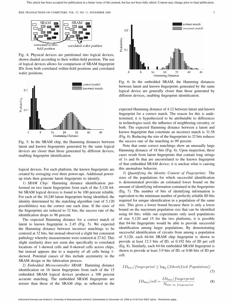
Fig. 4: Physical devices are partitioned into logical devices,
shown shaded according to their within-field position. The use
of logical devices allows for comparison of SRAM fingerprint
IDs from both correlated within-field positions and correlated
wafer positions.
Fig. 5: In the SRAM chip, the Hamming distances between
latent and known fingerprints generated by the same logical
devices are closer than those generated by different devices,
enabling fingerprint identification.
logical devices. For each platform, the known fingerprints are
created by averaging over three power-ups. Additional power-
up trials then generate latent fingerprints to identify.
1) SRAM Chip: Hamming distance identification per-
formed on two latent fingerprints from each of the 5,120 64-
bit SRAM logical devices is found to be 100 percent reliable.
For each of the 10,240 latent fingerprints being identified, the
identity determined by the matching algorithm (out of 5,120
possibilities) was the correct one each time. If the sizes of
the fingerprints are reduced to 32 bits, the success rate of the
identification drops to 96 percent.
The expected Hamming distance for a correct match of
latent to known fingerprint is 2.45 (Fig. 5). We expected
the Hamming distance between incorrect matchings to be
centered at 32 bits, but instead observed a slight but consistent
pathology whereby measurements were centered at 27.62. This
slight similarity does not seem due specifically to correlated
locations of 1-skewed cells and 0-skewed cells across chips,
but instead appears due to a majority of all cells being 1-
skewed. Potential causes of this include asymmetry in the
SRAM design or the fabrication process.
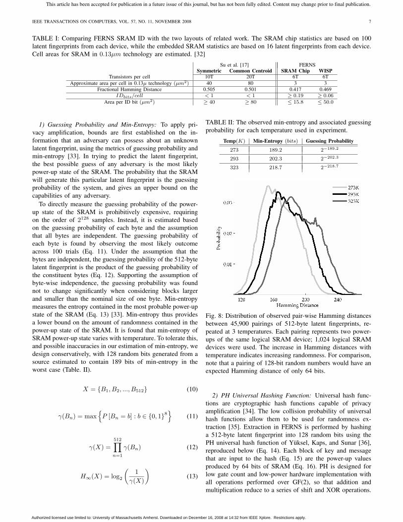
2) Embedded Microcontroller SRAM: Hamming distance
identification on 16 latent fingerprints from each of the 15
embedded SRAM logical devices produces a 100 percent
accurate matching. The embedded SRAM fingerprints are
noisier than those of the SRAM chip, as reflected in the
Fig. 6: In the embedded SRAM, the Hamming distances
between latent and known fingerprints generated by the same
logical device are generally closer than those generated by
different devices, enabling fingerprint identification.
expected Hamming distance of 4.12 between latent and known
fingerprint for a correct match. The reason for this is unde-
termined; it is hypothesized to be attributable to differences
in technologies used, the influence of neighboring circuitry, or
both. The expected Hamming distance between a latent and
known fingerprint that constitute an incorrect match is 31.58
(Fig. 6). Reducing the size of the fingerprints to 32 bits reduces
the success rate of the matching to 99 percent.
Note that some correct matchings show an unusually large
Hamming distance of 18 bits (Fig. 6). Upon inspection, these
cases result from latent fingerprints that contain long strings
of 1s and 0s that are uncorrelated to the known fingerprint
of that embedded SRAM device; it is unclear what is causing
this anomalous behavior.
3) Quantifying the Identity Content of Fingerprints: The
sizes of the populations for which successful identification
is demonstrated provides an estimated lower bound on the
amount of identifying information contained in the fingerprints
(Eq. 7). The number of bits of identifying information is
equivalent to the minimum number of perfectly reliable ID bits
required for unique identification in a population of the same
size. This gives a lower bound because there is only a lower
bound on the maximum population size that can be identified
using 64 bits; while our experiments only used populations
of size 5,120 and 15 for the two platforms, it is possible
that 64-bit fingerprints would be able to provide successful
identification among larger populations. By demonstrating
successful identification of circuits from among a population
of 5,120, each 64-bit SRAM chip fingerprint is shown to
provide at least 12.3 bits of ID, or 0.192 bits of ID per cell
(Eq. 8). Similarly, each 64-bit embedded SRAM fingerprint is
shown to provide at least 3.9 bits of ID, or 0.06 bits of ID per
cell.
IDbits/fingerprint ≥ log2 (|Identified Population|)(7)
IDbits/cell =IDbits/fingerprint
Nbits in fingerprint(8)
This article has been accepted for publication in a future issue of this journal, but has not been fully edited. Content may change prior to final publication.
Authorized licensed use limited to: University of Massachusetts Amherst. Downloaded on December 16, 2008 at 14:32 from IEEE Xplore. Restrictions apply.

IEEE TRANSACTIONS ON COMPUTERS, VOL. 57, NO. 11, NOVEMBER 2008 6
Area per ID bit =Area/cell
IDbits/cell(9)
Based on the amount of identity provided per cell, the
identifying ability of larger fingerprints is extrapolated. For
example, a 16-byte fingerprint from the SRAM chip (providing
0.192 bits of ID per cell) would provide 24.6 bits of ID,
sufficient for identification among a population of 224.6, over
26 million. This analysis is generalized to different size
fingerprints of both platforms in Fig.7.
Fig. 7: The size of population in which members can be
uniquely identified as a function of the size of the fingerprint,
for both the SRAM chip and embedded SRAM. The solid lines
are demonstrated through experiment, while the dashed lines
are extrapolated.
C. Comparison to existing work
With regards to the mechanism for generating ID based
on threshold voltage mismatch in cross-coupled devices, the
FERNS method is similar to, and inspired by, the recent ISSCC
2007 design of Su, Holleman, and Otis [17]. In this related
work, a cross-coupled NOR cell is used to generate the ID.
When the control signal is set low, the cross-coupled devices
are isolated from the supply and both state nodes are pulled
low; the circuit in this state is analogous to the cross-coupled
inverters in an unpowered SRAM cell. To obtain the ID, the
cross-coupled devices are connected to the supply rail, causing
the cell to stabilize to one of two stable states; the choice of
stable state represents the identity of the cell. This behavior is
analogous to the powering-up of an SRAM cell.
The design of Su et al. gives excellent performance, but it
comes at a high area cost; we present a case that this cost is
excessive. One reason for the excellent performance of this
design is the use of analog layout techniques to minimize
the impact of noise and correlated process effects. These
layout techniques minimize the number of unstable cells and
maximize the fractional Hamming distance across chips, but
also result in a low transistor density; the area of each ID cell
is 40μm2, and additional area is consumed by surrounding
the ID cells with dummy cells to ensure isolation from any
potential noise sources. Contrary to this specialized and sparse
layout, the large production quantities of conventional SRAM
cells justify a density-optimized layout, with cell areas of just
3μm2 at the same 0.13μm technology node [32].
With 13 SRAM cells consuming less total area than each
ID cell from Su’s design, comparing the per-cell identifying
ability of SRAM fingerprints to these ID cells does not give a
true measure of how efficiently each design is using chip area.
Instead, the designs are compared using a cost metric of area
per ID bit, calculated as area per cell divided by the amount
of usable identity generated by each cell (Eq. 9). This metric
is applied conservatively to FERNS by basing the amount of
identity contained in each SRAM cell on the lower bound of
what has been demonstrated (Eq. 7). The identifying ability
of the design of Su et al. is overestimated, by assuming that
each cell produces a perfect bit of identity.
According to this metric of area per ID bit, SRAM fin-
gerprints provide identification with comparable efficiency to
the work of Su et al. (Table. I). However, there are some
notable differences between how the two works can be applied.
The FERNS method has the advantage that the area used to
generate the identifying fingerprint is not dedicated to the
task, but is instead general purpose SRAM. A drawback to
the FERNS approach is that the identifier is only generated at
power-up, and is destroyed once data is written to the SRAM.
The fingerprint can only be regenerated by cycling the power
to the SRAM.
V. FERNS FOR TRUE RANDOM NUMBER GENERATION
Experiments show that 512 bytes of latent fingerprint can be
used to create a 128-bit true random number. As explained in
Section III, the neutral-skewed cells in the SRAM can power-
up to either state in the presence of noise. This causes latent
fingerprints to be randomized (Fig. 8). In essence, the neutral-
skewed SRAM cells function as tiny, imprecise, six transistor
TRNG circuits scattered across the SRAM array, generating
and storing random bits at power-up. This section deals with
how to quantify, extract, and evaluate the randomness for use
in FERNS.
Note that the experimental TRNG results are from the
SRAM chip and not the embedded SRAM, which has only 256
bytes of SRAM. The Hamming distance between latent and
known fingerprints generated by the same device is smaller for
SRAM chip design, indicating less randomness and implying
that the conclusions drawn from the SRAM chip would likely
also apply to the embedded SRAM design. Nonetheless, the
amount of randomness contained in any SRAM design should
be quantified before it is used for generating random numbers.
A. Entropy Extraction
To extract the randomness from the latent fingerprints,
privacy amplification is employed. In general terms, privacy
amplification techniques are used to extract a secret from a
body of information about which an adversary has partial
knowledge. Mapping privacy amplification to the domain of
this work, the extracted secret is the random number, the
body of information is the latent SRAM fingerprint generated
at power-up, and the partial knowledge of the adversary is
knowledge of the tendency of each SRAM cell.
This article has been accepted for publication in a future issue of this journal, but has not been fully edited. Content may change prior to final publication.
Authorized licensed use limited to: University of Massachusetts Amherst. Downloaded on December 16, 2008 at 14:32 from IEEE Xplore. Restrictions apply.
IEEE TRANSACTIONS ON COMPUTERS, VOL. 57, NO. 11, NOVEMBER 2008 7
TABLE I: Comparing FERNS SRAM ID with the two layouts of related work. The SRAM chip statistics are based on 100
latent fingerprints from each device, while the embedded SRAM statistics are based on 16 latent fingerprints from each device.
Cell areas for SRAM in 0.13μm technology are estimated. [32]
Su et al. [17] FERNSSymmetric Common Centroid SRAM Chip WISP
Transistors per cell 10T 20T 6T 6T
Approximate area per cell in 0.13μ technology (μm2) 40 80 3 3Fractional Hamming Distance 0.505 0.501 0.417 0.469
IDbits/cell < 1 < 1 ≥ 0.19 ≥ 0.06Area per ID bit (μm2) ≥ 40 ≥ 80 ≤ 15.8 ≤ 50.0
1) Guessing Probability and Min-Entropy: To apply pri-
vacy amplification, bounds are first established on the in-
formation that an adversary can possess about an unknown
latent fingerprint, using the metrics of guessing probability and
min-entropy [33]. In trying to predict the latent fingerprint,
the best possible guess of any adversary is the most likely
power-up state of the SRAM. The probability that the SRAM
will generate this particular latent fingerprint is the guessing
probability of the system, and gives an upper bound on the
capabilities of any adversary.
To directly measure the guessing probability of the power-
up state of the SRAM is prohibitively expensive, requiring
on the order of 2128 samples. Instead, it is estimated based
on the guessing probability of each byte and the assumption
that all bytes are independent. The guessing probability of
each byte is found by observing the most likely outcome
across 100 trials (Eq. 11). Under the assumption that the
bytes are independent, the guessing probability of the 512-byte
latent fingerprint is the product of the guessing probability of
the constituent bytes (Eq. 12). Supporting the assumption of
byte-wise independence, the guessing probability was found
not to change significantly when considering blocks larger
and smaller than the nominal size of one byte. Min-entropy
measures the entropy contained in the most probable power-up
state of the SRAM (Eq. 13) [33]. Min-entropy thus provides
a lower bound on the amount of randomness contained in the
power-up state of the SRAM. It is found that min-entropy of
SRAM power-up state varies with temperature. To tolerate this,
and possible inaccuracies in our estimation of min-entropy, we
design conservatively, with 128 random bits generated from a
source estimated to contain 189 bits of min-entropy in the
worst case (Table. II).
X = {B1, B2, ..., B512} (10)
γ(Bn) = max{
P [Bn = b] : b ∈ {0, 1}8}
(11)
γ(X) =512∏n=1
γ(Bn) (12)
H∞(X) = log2
(1
γ(X)
)(13)
TABLE II: The observed min-entropy and associated guessing
probability for each temperature used in experiment.
Temp(K) Min-Entropy (bits) Guessing Probability
273 189.2 2−189.2
293 202.3 2−202.3
323 218.7 2−218.7
Fig. 8: Distribution of observed pair-wise Hamming distances
between 45,900 pairings of 512-byte latent fingerprints, re-
peated at 3 temperatures. Each pairing represents two power-
ups of the same logical SRAM device; 1,024 logical SRAM
devices were used. The increase in Hamming distances with
temperature indicates increasing randomness. For comparison,
note that a pairing of 128-bit random numbers would have an
expected Hamming distance of only 64 bits.
2) PH Universal Hashing Function: Universal hash func-
tions are cryptographic hash functions capable of privacy
amplification [34]. The low collision probability of universal
hash functions allow them to be used for randomness ex-
traction [35]. Extraction in FERNS is performed by hashing
a 512-byte latent fingerprint into 128 random bits using the
PH universal hash function of Yuksel, Kaps, and Sunar [36],
reproduced below (Eq. 14). Each block of key and message
that are input to the hash (Eq. 15) are the power-up values
produced by 64 bits of SRAM (Eq. 16). PH is designed for
low gate count and low-power hardware implementation with
all operations performed over GF(2), so that addition and
multiplication reduce to a series of shift and XOR operations.
This article has been accepted for publication in a future issue of this journal, but has not been fully edited. Content may change prior to final publication.
Authorized licensed use limited to: University of Massachusetts Amherst. Downloaded on December 16, 2008 at 14:32 from IEEE Xplore. Restrictions apply.

IEEE TRANSACTIONS ON COMPUTERS, VOL. 57, NO. 11, NOVEMBER 2008 8
PHK (M) =16∑
i=1
(m2i−1 + k2i−1) (m2i + k2i) (14)
M = (m1, ...,m32) K = (k1, ..., k32) (15)
mi, ki ∈ GF (2) (16)
3) Statistical Testing of Extracted Random Bits: While min-
entropy is intended as the primary assurance of randomness
for the generated bits, these bits are also tested using the
runs, approximate entropy, and block frequency tests from the
NIST suite [37]. Over 52 million bits of power-up state are
hashed into 12,800 128-bit random numbers for testing. As a
compromise between testing large blocks of random bits and
testing many blocks of random bits, the tests are performed
on 1,280 blocks of 1,280 bits each, with each block being
a concatenation of ten 128-bit random numbers. The random
numbers pass each of the tests (Table. III), further supporting
the feasibility of extracting statistically random numbers from
the power-up state of ordinary commercial SRAM chips using
a simple low-cost entropy extracting code.
B. Comparison to Existing Work
With regards to the mechanism for generating entropy,
the FERNS method is compared to, and contrasted against,
the recent ISSCC 2007 TRNG design of Tokunaga, Blaauw
and Mudge [30]. Both designs create random numbers us-
ing metastable cross-coupled CMOS devices. In Tokunaga’s
design, a single cross-coupled cell is biased precisely to the
metastable point and then allowed to stabilize, with the stable
state then determined by noise. Because the the metastable bias
point is not static, dynamic control and feedback are used to
set the cell to the metastable point. A delay test is used to
judge the metastability; the probability that the bias point is
truly metastable increases with the time required to resolve
the metastability. A notable benefit of this approach is that the
bits produced are assured to be a result of thermal noise, but
a drawback is that having a high precision timer and control
system consumes power and area.
The FERNS method of extracting randomness from SRAM
is akin to using a very imprecise version of Tokunaga’s
design. In FERNS, massive redundancy compensates for the
imprecision, with the randomness scattered throughout the
SRAM (Fig. 9). No feedback or control is required, because
there is no need to precisely bias a single cross-coupled cell
to perfect metastability. Instead, FERNS relies on the large
number of cells to ensure that some cells will be influenced
by noise when the chip is powered-up, without giving concern
to which cells are generating randomness. In fact, when the
chip is powered-up in different conditions, different cells
become random (See Section VI-B), demonstrating a potential
resiliency against external influences.
1) Estimated Area Costs: The tradeoff of precision against
redundancy has implications on the area cost. In Tokunaga’s
circuit, the majority of silicon area is consumed by the control
logic. The metastable module itself is approximately the size
of 600 SRAM cells. Because FERNS is using 512 bytes of
Fig. 9: SRAM cells with unpredictable power-up states, shaded
dark, are scattered throughout a 512-byte section – the quantity
used to create a single 128-bit random number. The entropy
of each cell is determined from 100 power-ups at 293 K. Note
that the measure entropy differs from the measure min-entropy,
as min-entropy is meaningless for single bits.
TABLE IV: Comparing the estimated area of FERNS with that
of related work, based on 0.13μm technology
Tokunaga et al. [30] FERNSFunction Area(μm2) Function Area(μm2)
Metastable Module 6,000 SRAM Array 12,300Control 29,900 PH Hashing 7,400Total 35,900 Total 19,700
SRAM, FERNS requires more area for its metastable circuitry.
However, the PH universal hashing function, requiring only
557 cells, is roughly a quarter of the size of the counter and
charge injection circuitry required for the Tokunaga’s circuit.
Note that our estimates for area comparison are indirectly
supported by the related work itself, as the ISSCC2007 die
micrograph shows an 8 kbyte SRAM array side-by-side with
the TRNG circuit. [30].
2) Fixed vs. Unlimited Entropy Generation: The primary
limitation of the FERNS TRNG is that entropy is only
generated during power-up. This contrasts poorly against the
unbounded entropy generation potential any dedicated TRNG
circuit. If random numbers will be needed during a time other
than power-up, the random numbers must be extracted and
stored from power-up until use. For this reason, the FERNS
method is best suited to applications that are intermittently-
powered and do not require large quantities of random num-
bers.
3) Custom vs. General Purpose Circuitry: The preceding
paragraphs have shown that FERNS can generate random
numbers in comparable area to a dedicated circuit, but is
greatly limited in the amount of randomness it can generate
on account of only being able to generate entropy at power-
up; not a very compelling case for FERNS TRNG thus far.
The strength of the FERNS method is the ability to generate
true random numbers without any dedicated circuitry. Both the
hash function and the SRAM itself are common parts which
can be reused, helping to amortize the area cost. In embedded
applications such as RFID or smart cards, a cryptographic hash
function is likely to be pre-existing for security functionality.
This article has been accepted for publication in a future issue of this journal, but has not been fully edited. Content may change prior to final publication.
Authorized licensed use limited to: University of Massachusetts Amherst. Downloaded on December 16, 2008 at 14:32 from IEEE Xplore. Restrictions apply.

IEEE TRANSACTIONS ON COMPUTERS, VOL. 57, NO. 11, NOVEMBER 2008 9
TABLE III: Output from NIST tests for runs, approximate entropy and block frequency, applied to the random numbers
produced by FERNS. The uniform distribution across columns c1 through c10 indicate a uniform distribution for the frequency
of various P-values. The 11th column indicates the P-value obtained via a chi-square test. The 12th column indicates the
proportion of binary sequences that passed testing. The random numbers generated by FERNS pass each test.
C1 C2 C3 C4 C5 C6 C7 C8 C9 C10 P VAL PROP TEST134 131 129 126 129 108 131 119 139 134 0.7931 0.9922 runs139 122 124 132 138 124 122 120 126 133 0.9467 0.9945 apen119 124 147 121 125 116 147 134 130 117 0.4159 0.9898 block-frequency
In a microcontroller, the PH hashing can be performed using
only XOR and bitshift operations that are found as primitives
in nearly all instruction set architectures. Thus, our use of
such a hash function constitutes a reuse of an existing part.
By offering TRNG using commonly available circuitry, the
FERNS method may enable TRNG in some applications that
were previously incapable of it.
VI. ROBUSTNESS TO ENVIRONMENTAL FACTORS
The viability of the FERNS method depends on how sensi-
tive the fingerprint identity and TRNG are to the environments
where the circuit will be used. This section explores the
potential influence of supply voltage, ambient temperature, and
negative bias temperature instability on power-up SRAM state.
A. Supply Voltage
The ability of an SRAM cell to hold state depends on
noise, the process variation of the cell, and the applied supply
voltage. Low supply voltage leaves a cell susceptible to noise-
induced state changes, while higher voltage makes a cell stable
and immune to noise. The minimum supply voltage at which
an SRAM cell is able to tolerate ’reasonable’ noise without
changing state varies from cell to cell, is determined by vari-
ation, and typically falls in the range of 100 to 300 mV [38].
During power-up, it is assumed that the supply voltage begins
at 0 V where all cells can be influenced by noise, and increases
to a nominal operating voltage well above 300 mV, where all
cells are stable in the 0 or 1 state and not influenced by noise.
The randomness and identity in power-up SRAM state is thus
determined by cell behaviors at low supply voltages.
Static Noise Margin (SNM) is the metric for quantifying the
noise-immunity of an SRAM cell. The SNM of a cell at given
supply voltage is defined as the maximum noise voltage that
can be tolerated before changing state [39]. SNM is measured
as the shortest side of the largest box that can be placed
inside of the eye of the Voltage Transfer Curves (VTCs) of
the cross-coupled inverters that comprise the cell [40], [41].
A noise-immune cell has two large eyes between the inverter
VTCs. SNM is greatly diminished at low supply voltages (Fig.
10). In cells that are not skewed by variation, low supply
voltage causes the SNM of each state to be equally small (Fig.
10a). However, in highly skewed cells, low supply voltage can
reduce the SNM of one state to 0 V, indicating the existence
of a single noise-immune state (Fig. 10b).1) Relevance to FERNS method: By controlling how
quickly the supply voltage ramps up, it may be possible to
influence the power-up state to be less random. Consider the
case of the skewed SRAM cell described by the VTCs in
(a) SNMs of unskewed cell (b) SNMs of 0-skewed cell
Fig. 10: VTCs obtained from SPICE simulation of a skewed
and neutral SRAM cell at 100 and 250 mV supply. At 100 mV,
the skewed cell will transition to the 0 state and remain there.
Fig. 10b. If the supply voltage is held at 100 mV during power-
up, even the slightest noise will induce a transition to the 0
state favored by this cell. The probability of this transition
increases with the amount of time that the supply is held at
100 mV. Note that there is nothing unique about this particular
cell or supply voltage; any skewed cell will have some voltage
at which a transition to the favored state is inevitable, given
sufficient time. By increasing the supply voltage very slowly,
one could likely create an exceptionally identifying power-up
fingerprint with an increased number of cells powering-up to
their favored state. If an adversary could control the supply
voltage in this way, he might be able to reduce the entropy
of the random numbers extracted from the SRAM power-up
fingerprints.
B. Impact of Temperature
While the temperature of high performance VLSI circuits
can exceed 400 K, the range of temperatures relevant to
FERNS is modest by comparison because SRAM fingerprints
are generated at power-up before any self-heating has oc-
curred. To represent extreme ambient temperatures that an
SRAM might encounter at power-up, experiments are per-
formed at 273 K (freezing point of water), 293 K (room tem-
perature), and 323 K (among the hottest recorded temperatures
on earth).
The impact of temperature on MOSFET devices is well
studied in literature. An increase in temperature decreases
device threshold voltages (Eq. 17), while also decreasing the
electron and hole mobilities (Eq. 18) [42]. These two trends
may counteract each other during power-up, since a lowered
threshold will increase subthreshold current, while reduced
This article has been accepted for publication in a future issue of this journal, but has not been fully edited. Content may change prior to final publication.
Authorized licensed use limited to: University of Massachusetts Amherst. Downloaded on December 16, 2008 at 14:32 from IEEE Xplore. Restrictions apply.

IEEE TRANSACTIONS ON COMPUTERS, VOL. 57, NO. 11, NOVEMBER 2008 10
TABLE V: Estimated thermal noise, threshold voltages, and
mobilities at experiment temperatures.
T (K) σ2noise(μV )
VTH(mV ) μ(cm2/V s)P N P N
273 17.5 311 474 555 1727293 18.8 288 452 482 1499323 20.7 254 419 451 1402
mobility will decrease subthreshold current. Additionally, an
increase in temperature increases the magnitude of thermal
noise (Eq. 19), which could lead to a more random power-
up state. The estimated thermal noise, threshold voltages and
carrier mobilities for each temperature are given in Table V;
threshold voltages are obtained from 0.18μm BSIM3 mod-
els [43], thermal noise is calculated based on 0.430 fF node
capacitances, and mobilities are calculated using values of -2
for α and 480 and 1350 cm2/V s for μ0p and μ0n respectively.
The influence of these changing MOSFET characteristics on
SRAM power-up state is difficult to model because power-up
state is not determined directly by the MOSFET devices, but
instead by the relative strength of cross-coupled devices that
are similarly impacted by temperature.
Vth(T ) = Vth(To) − κΔT (17)
μ(T ) = μ0
(T
300
)α
(18)
σ2NOISE(T ) =
2KBT
C(19)
1) Observed Tendencies of Neutral Cells: Determining how
the skew of an SRAM cell changes with temperature is
challenging, as the only measurement that can be made is
p, the probability of a given cell initializing to 1 (Eq. 2).
The power-up tendencies of neutral-skewed cells can provide
some insights on the influence of temperature. On a 512 kbyte
SRAM chip under nominal conditions, over 30,000 cells are
found to be neutral (p293 is 0.5). The same chip is powered-up
10 times at each of the other temperatures, and the tendencies
of these neutral cells are observed; each one can then be
classified as a triple of p values (p273 , p293 , p323). The contour
plot of Fig.11 shows the distribution of observed triples; Note
that p293 does not appear explicitly, since all cells contributing
to the distribution have 0.5 for p293 . The data in this plot leads
to three insights regarding how the power-up tendencies of
cells shift with temperature.
1) The skew of a cell can change with temperature.Cells that are neutral at 293 K are typically not also
neutral at other temperatures. Instead, the majority of
these cells become 0-skewed or 1-skewed when the
temperature is changed. This is indicated by the rel-
atively low probabilities around (0.5273 , 0.5293 , 0.5323),and the significantly higher probabilities occurring at
(0273 , 0.5293 , 1323) and (1273 , 0.5293 , 0323).2) Skew shift is monotonic with respect to temperature.
If an increase in temperature makes a neutral cell
become 1-skewed, then decreasing the temperature will
Fig. 11: This contour shows the probability distribution at
273 K and 323 K, of all cells that are neutral at 293 K. Note
that the probability exceeds 0.04 at the highest points; these
peaks are omitted to show the rest of the distribution with
greater detail. See Section VI-B1 for discussion
typically make that same cell 0-skewed. This trend is
observed in the high probabilities at (0273 , 0.5293 , 1323)and (1273 , 0.5293 , 0323) compared to the lower probabil-
ities at (1273 , 0.5293 , 1323) and (0273 , 0.5293 , 0323).3) The direction of skew shift differs from cell to cell.
Although individual cell tendencies do change mono-
tonically with temperature, they do not all shift in the
same direction. Of the cells that are neutral at 293 K,
some become 1-skewed at higher temperatures and 0-
skewed at lower temperatures, while the opposite trend
is seen in other cells. This is observed in the high
probabilities occurring at both (0273 , 0.5293 , 1323) and
(1273 , 0.5293 , 0323).
2) Relevance to FERNS method: Temperature is only a
minor concern for the quality of identification and random
numbers produced in FERNS. Although the 50 mV threshold
shift across the range of experiment temperatures are approx-
imately twice the standard deviation of the device thresholds,
the ID in FERNS only depends on the relative strengths of the
two cross-coupled inverters (see Section III-A). The common-
mode effects of temperature do not significantly favor one state
over the other. Experiments show that Hamming distances
between known fingerprints generated at 293 K and latent
fingerprints taken at 273 K or 323 K are only slightly larger
than those obtained when both latent and known fingerprint
are generated at 293 K (Fig. 12).
The min-entropy of SRAM fingerprints increases with tem-
perature (Table. II). However, without being able to properly
attribute this to an increase in thermal noise, it is unknown
whether an adversary could use temperature to influence the
quality of the TRNG. With this in mind, the TRNG is designed
conservatively; in the worst case (273 K), an estimated 189
bits of min-entropy are used to create 128 random bits. Larger
SRAM fingerprints can be used if a greater assurance of
entropy is desired.
This article has been accepted for publication in a future issue of this journal, but has not been fully edited. Content may change prior to final publication.
Authorized licensed use limited to: University of Massachusetts Amherst. Downloaded on December 16, 2008 at 14:32 from IEEE Xplore. Restrictions apply.

IEEE TRANSACTIONS ON COMPUTERS, VOL. 57, NO. 11, NOVEMBER 2008 11
Fig. 12: Matching the nominal known fingerprints against
latent fingerprints taken at different temperatures shows that
fingerprint IDs change only slightly with temperature.
Fig. 13: NBTI raises the threshold of stressed PMOS device
M3 and skews the power-up state of the cell away from the 0
state (AB=01) that was causing the stress.
C. Negative Bias Temperature Instability
Prior work in secure hardware has shown that storing data in
SRAM cells for long periods of time can cause burn-in, allow-
ing the data to be reconstructed long after it was stored [44].
A modern version of burn-in to consider is Negative Bias
Temperature Instability (NBTI). NBTI is a phenomenon by
which deep submicron MOSFET threshold voltages increase
over time due to applied stress conditions of high temperature
and a vertical electric field caused by the voltage at the
MOSFET gate terminal. This electric field creates the inversion
channel that allows the MOSFET to conduct current, and is
present whenever a device is turned on. The NBTI-induced
increase in threshold voltage grows with the amount of time
that the stress conditions are applied [45]. Once the stress is
removed, devices begin to recover; in cases where only a high
gate voltage is applied without high temperature, recovery can
reach 100 percent [46]. While NBTI can impact both PMOS
and NMOS devices, PMOS NBTI dominates [47].
1) Analysis of NBTI Impact: NBTI causes the skew of
each SRAM cell to shift away from the value previously
stored by the cell. Consider a slightly 0-skewed SRAM cell
that stores a 0 (AB=01), as depicted in Fig.13. Device M3
TABLE VI: Observed average Hamming weights before and
after NBTI stress.
Stress Time(s) Recovery Time(s) Hamming Weight8.6 ∗ 105 20 0.7749
1.7 ∗ 105 20 0.76261.7 ∗ 105 180 0.75611.7 ∗ 105 420 0.7527
Baseline - 1 0.7508Baseline - 2 0.7510Baseline - 3 0.7508Baseline - 4 0.7507
experiences NBTI stress conditions while the cell stores the 0,
and consequently has an increased threshold voltage afterward.
The next time this cell is powered-up, the higher threshold
voltage of M3 (neglecting recovery) causes it to turn on more
slowly than normal, making the cell less likely to power-up to
0 (AB=01) than it was before NBTI stress, and more likely to
power-up to the opposing 1 state.
2) NBTI Burn-in Experiments: The conclusion that NBTI
causes a cell storing a given value to favor the opposite
value in the next power-up is supported by four NBTI burn-in
experiments. Each experiment is performed sequentially on
the same 512 kbyte SRAM chip, and takes the following
form: 1) Power-up SRAM at 313 K and write 0 into all
cells; 2) Maintain power and temperature, burning-in the 0
state for specified stress time; 3) Power down SRAM and
remain powered-down for specified recovery time; 4) Power-
up SRAM again and read out state to determine Hamming
weight.
Three of the experiments use a burn-in of 1.7 × 10⁵
seconds (two days) with varied recovery times, and the fourth
experiment uses a longer burn-in time of 8.6 × 10⁵ seconds
(ten days). The Hamming weights from each are compared
to a set of previously obtained baseline measurements taken
at room temperature under nominal conditions. In all four
experiments, the average Hamming weight of the SRAM cells
increased significantly after burning-in the 0 state, consistent
with prediction. Substantial NBTI recovery is observed, but
full recovery does not occur within 420 seconds (Table. VI).
3) Relevance to FERNS method: Normal usage patterns of
intermittently-powered devices operating at low temperatures
should prevent incidental NBTI from being a significant con-
cern. However, if used maliciously under atypical conditions,
NBTI could be a threat to FERNS because it provides a
way to skew each cell toward a chosen power-up state. This
is illustrated by contrasting the impact of NBTI against the
impact of varying SRAM temperature (Fig. 14), when both
are applied to the same 512 kbyte SRAM chip. All cells
are first classified according to their p values (Eq. 2) under
nominal conditions. When the chip is then powered-up at
one temperature, the expected value (E(p)) of the power-up
state of all cells in each p classification is calculated; this is
repeated for temperatures 273, 293, and 323 K, and for NBTI
burn-in durations of 1.7 × 10⁵ and 8.6 × 10⁵ seconds (both
with 20 second recovery time). The NBTI burn-in of the 0
state skews cells across all nominal probabilities toward the
1 state; for example, among all cells that have a 50 percent
This article has been accepted for publication in a future issue of this journal, but has not been fully edited. Content may change prior to final publication.
Authorized licensed use limited to: University of Massachusetts Amherst. Downloaded on December 16, 2008 at 14:32 from IEEE Xplore. Restrictions apply.

IEEE TRANSACTIONS ON COMPUTERS, VOL. 57, NO. 11, NOVEMBER 2008 12
Fig. 14: The expected value of the power-up state of a cell
at varied temperature, or after NBTI stress, is plotted as a
function of the probability p of the same cells powering-up to
1 under nominal conditions. Using NBTI to burn-in 0 values
causes cells of all nominal probabilities to be slightly more
likely to power-up to the 1 state, while varying temperature
induces random shifts, causing the expected value of cells of
all nominal probabilities to tend toward 0.5
probability of powering-up to 1 under nominal conditions, 59
percent power-up to 1 after the moderate NBTI burn-in, and
68 percent power-up to 1 after the longer burn-in. Across all
nominal tendencies, NBTI burn-in of the 0 state causes cells to
become more likely to power-up to the 1 state. This predictable
influence of NBTI stands in contrast to the unpredictable skew
shifts induced by increasing or decreasing temperature, which
overall cause the expected values to trend toward 0.5 across
all nominal p skews.
VII. CONCLUSIONS AND FUTURE WORK
In this paper, we have presented the FERNS method for
using SRAM physical fingerprints to identify circuits and
generate true random numbers. We show that the power-
up state of just 8 bytes of a commercially available SRAM
are sufficient for identification among a population of 5,120
instances, and that 512 bytes of the same SRAM produce
enough randomness to generate 128-bit numbers capable of
passing statistical tests for randomness. The identity in the
SRAM fingerprint comes from the inherent threshold voltage
mismatch of MOSFET devices, and the randomness results
from noise impacting SRAM cells that do not have significant
mismatch.
The strength of the FERNS method is that no dedicated
circuits are required. Aside from the SRAM used to generate
the fingerprints, the randomness extraction requires only a
hash function or simple processing core capable of bitshift
and bitwise XOR operations. Given the ubiquity of these
enabling parts, we believe that FERNS can find use across the
spectrum of integrated circuit applications, ranging from low
cost passively-powered RFID tags and smart cards up through
embedded caches on high-end devices.
Future work on FERNS will include a custom-
implementation of a derivative design, and exploring
the effectiveness of the potential attacks discussed in this
paper.
ACKNOWLEDGMENTS
We thank Thomas Heydt-Benjamin for his discussion on
potential applications for SRAM physical fingerprints, Intel
Research and Joshua R. Smith for providing and supporting
the WISP platforms, and Adam Stubblefield for reviewing an
early manuscript and providing feedback that has helped to
guide the development of this work. We thank the anonymous
reviewers for their insightful and constructive comments on
this work.
REFERENCES
[1] I. Goldberg and D. Wagner, “Randomness and the netscape browser,”Dr. Dobbs Journal, p. 6670, 1996.
[2] T. S. Heydt-Benjamin, D. V. Bailey, K. Fu, A. Juels, andT. O’Hare, “Vulnerabilities in First-Generation RFID-enabled CreditCards,” in Proceedings of Eleventh International Conference onFinancial Cryptography and Data Security, Lowlands, Scarborough,Trinidad/Tobago, February 2007. [Online]. Available: http://prisms.cs.umass.edu/∼kevinfu/papers/RFID-CC-manuscript.pdf
[3] D. Halperin, T. S. Heydt-Benjamin, B. Ransford, S. S. Clark, B. Defend,W. Morgan, K. Fu, T. Kohno, and W. H. Maisel, “Pacemakers andimplantable cardiac defibrillators: Software rad io attacks and zero-power defenses,” in Proceedings of the 29th Annual IEEE Symposiumon Security and Privacy, May 2008.
[4] D. E. Holcomb, W. P. Burleson, and K. Fu, “Initial SRAM state asa fingerprint and source of true random numbers for RFID tags,” inProceedings of the Conference on RFID Security, July 2007.
[5] IS61LV25616AL - 256K x 16 High Speed Asynchronous CMOS StaticRAM With 3.3V Supply, Integrated Silicon Solution, Inc., Feb 2006.[Online]. Available: http://www.issi.com/pdf/61LV25616AL.pdf
[6] Altera’s Development and Education Board, Altera Corporation, 2007.[Online]. Available: http://www.altera.com/education/univ/materials/boards/unv-de2-board.html
[7] J. R. Smith, A. Sample, P. Powledge, S. Roy, and A. Mamishev, “Awirelessly-powered platform for sensing and computation,” in Proceed-ings of Ubicomp 2006: 8th International Conference on UbiquitousComputing, 2006, pp. 495–506.
[8] A. P. Sample, D. J. Yeager, P. S. Powledge, and J. R. Smith, “Design of apassively-powered, programmable platform for UHF RFID systems,” inProceedings of IEEE International Conference on RFID, March 2007,pp. 149–156.
[9] A. P. Sample, D. J. Yeager, P. S. Powledge, A. V. Mamishev, and J. R.Smith, “Design of an RFID-based battery-free programmable sensingplatform,” Instrumentation and Measurement, IEEE Transactions on,vol. 57, no. 11, pp. 2608–2615, Nov. 2008.
[10] D. C. Ranasinghe, D. Lim, P. H. Cole, and S. Devadas, “White paper:A low cost solution to authentication in passive RFID systems,” Auto-ID Labs, The University of Adelaide, Adelaide, Australia, Tech. Rep.WP-HARDWARE-029, September 2006.
[11] Texas Instruments, MSP430x11x2 MSP430x12x2 Mixed SignalMicrocontroller, Aug 2004. [Online]. Available: http://focus.ti.com/lit/ds/symlink/msp430f1232.pdf
[12] W. D. Brown and J. E. Brewer, Eds., Nonvolatile Semiconductor MemoryTechnology: A Comprehensive Guide to Understanding and UsingNVSM Devices. Wiley-IEEE Press, 1997.
[13] P. Friedberg, W. Cheung, and C. Spanos, “Spatial variability of criticaldimensions,” in VLSI/ULSI Multilevel Interconnection Conference XXII,2005, pp. 539–546.
This article has been accepted for publication in a future issue of this journal, but has not been fully edited. Content may change prior to final publication.
Authorized licensed use limited to: University of Massachusetts Amherst. Downloaded on December 16, 2008 at 14:32 from IEEE Xplore. Restrictions apply.

IEEE TRANSACTIONS ON COMPUTERS, VOL. 57, NO. 11, NOVEMBER 2008 13
[14] X. Tang, V. K. De, and J. D. Meindl, “Intrinsic MOSFET parameterfluctuations due to random dopant placement,” IEEE Transactions onVery Large Scale Integration (VLSI) Systems, pp. 369–376, December1997.
[15] ITRS, “Design,” International Technology Roadmap for Semiconductors,2006 Update.
[16] K. Lofstrom, W. Daasch, and D. Taylor, “IC identification circuitusing device mismatch,” in Digest of Technical Papers, 2000 IEEEInternational Solid-State Circuits Conference, 2000, pp. 372–373.
[17] Y. Su, J. Holleman, and B. Otis, “A 1.6pJ/bit 96% stable chip IDgenerating circuit using process variations,” in Digest of TechnicalPapers, 2007 IEEE International Solid-State Circuits Conference, 2007.
[18] P. Layman, S. Chaudhry, J. G. Norman, and J. R. Thomson, “Electronicfingerprinting of semiconductor integrated circuits,” Patent 6,738,294,September, 2002.
[19] R. S. Pappu, B. Recht, J. Taylor, and N. Gershenfeld, “Physical one-wayfunctions,” Science, vol. 297, no. 6, pp. 2026–2030, 2002, available athttp://web.media.mit.edu/∼brecht/papers/02.PapEA.powf.pdf.
[20] P. Tuyls, G.-J. Schrijen, B. Skoric, J. van Geloven, N. Verhaegh,and R. Wolters, “Read-Proof Hardware from Protective Coatings,” inCryptographic Hardware and Embedded Systems — CHES 2006, ser.Lecture Notes in Computer Science, vol. 4249. Springer, October 10-13, 2006, pp. 369–383.
[21] G. DeJean and D. Kirovski, “RF-DNA: Radio-frequency certificates ofauthenticity,” in CHES, 2007, pp. 346–363.
[22] B. Gassend, D. Clarke, M. van Dijk, and S. Devadas, “Silicon physicalrandom functions,” in Proceedings of the 9th ACM Conference onComputer and Communications Security, 2002, pp. 372–373.
[23] G. Suh, C. O’Donnell, I. Sachdev, and S. Devadas, “Design and im-plementation of the AEGIS single-chip secure processor using physicalrandom functions,” in Proceedings of 32nd International Symposium onComputer Architecture, 2005, pp. 25–36.
[24] J. Guajardo, S. S. Kumar, G.-J. Schrijen, and P. Tuyls, “FPGA intrinsicPUFs and their use for IP protection,” in Proceedings of the Workshopon Cryptographic Hardware and Embedded Security, September 2007,pp. 63–80.
[25] J. Guajardo, S. Kumar, G.-J. Schrijen, and P. Tuyls, “Physical unclon-able functions and public-key crypto for FPGA IP protection,” FieldProgrammable Logic and Applications, 2007. FPL 2007. InternationalConference on, pp. 189–195, Aug. 2007.
[26] H. Nyquist, “Thermal agitation of electric charge in conductors,” Phys.Rev. 32, 110, 1928.
[27] J. Johnson, “Thermal agitation of electricity in conductors,” Phys. Rev.32, 97, 1928.
[28] B. Sunar, W. J. Martin, and D. R. Stinson, “A provably secure truerandom number generator with built-in tolerance to active attacks,” IEEETransactions on Computers, vol. 58, pp. 109–119, Jan 2007.
[29] D. J. Kinnimet and E. Chester, “Design of an on-chip random numbergenerator using metastability,” in Proceedings of the 28th EuropeanSolid-State Circuits Conference, ESSCIRC 2002, 2002, pp. 595–598.
[30] C. Tokunaga, D. Blaauw, and T. Mudge, “A true random number gener-ator with a metastability-based quality control,” in Digest of Technicalpapers, 2007 IEEE International Solid-State Circuits Conference, 2007.
[31] J. M. Rabaey, A. Chandrakasan, and B. Nikolic, Digital IntegratedCircuits: A Design Perspective, 2nd ed. Prentice Hall, 2003.
[32] K. Osada, Y. Saitoh, E. Ibe, and K. Ishibashi, “16.7-fa/cell tunnel-leakage-suppressed 16-Mb SRAM for handling cosmic-ray-induced mul-tierrors,” Solid-State Circuits, IEEE Journal of, vol. 38, no. 11, pp. 1952–1957, Nov. 2003.
[33] V. Shoup, A computational introduction to number theory and algebra.Cambridge University Press, 2005.
[34] L. Carter and M. N. Wegman, “Universal classes of hash functions.” J.Comput. Syst. Sci., vol. 18, no. 2, pp. 143–154, 1979.
[35] N. Nisan and A. Ta-Shma, “Extracting randomness: A survey and newconstructions,” Journal of Computer and System Sciences, vol. 58, no. 1,pp. 148–173, 1999.
[36] K. Yuksel, J. P. Kaps, and B. Sunar, “Universal hash functions for emerg-ing ultra-low-power networks,” in Proceedings of The CommunicationsNetworks and Distributed Systems Modeling and Simulation Conference,Jan 2004.
[37] Rukhin et al, “A statistical test suite for random and pseudorandom num-ber generators for cryptographic applications,” NIST Special Publication800-22 (revised May 15 2002), 2002.
[38] H. Qin, Y. Cao, D. Markovic, A. Vladimirescu, and J. Rabaey, “SRAMleakage suppression by minimizing standby supply voltage,” QualityElectronic Design, 2004. Proceedings. 5th International Symposium on,pp. 55–60, 2004.
[39] E. Seevinck, F. List, and J. Lohstroh, “Static-noise margin analysis ofMOS SRAM cells,” Solid-State Circuits, IEEE Journal of, vol. 22, no. 5,pp. 748–754, Oct 1987.
[40] K. Agarwal and S. Nassif, “Statistical analysis of SRAM cell stability,”Design Automation Conference, 2006 43rd ACM/IEEE, pp. 57–62, July2006.
[41] A. Bhavnagarwala, X. Tang, and J. Meindl, “The impact of intrinsicdevice fluctuations on CMOS SRAM cell stability,” Solid-State Circuits,IEEE Journal of, vol. 36, no. 4, pp. 658–665, Apr 2001.
[42] S. Selberherr, “MOS device modeling at 77 k,” Electron Devices, IEEETransactions on, vol. 36, no. 8, pp. 1464–1474, Aug 1989.
[43] Y. Cao, T. Sato, D. Sylvester, M. Orshansky, and C. Hu, New paradigmof predictive MOSFET and interconnect modeling for early circuitdesign, 2001.
[44] R. Anderson and M. Kuhn, “Low cost attacks on tamper resistantdevices,” in IWSP: International Workshop on Security Protocols, LNCS,1997. [Online]. Available: citeseer.ist.psu.edu/anderson97low.html
[45] S. Mahapatra and M. Alam, “A predictive reliability model for PMOSbias temperature degradation,” Electron Devices Meeting, 2002. IEDM’02. Digest. International, pp. 505–508, 2002.
[46] S. Rangan, N. Mielke, and E. Yeh, “Universal recovery behavior ofnegative bias temperature instability,” Electron Devices Meeting, 2003.IEDM ’03 Technical Digest. IEEE International, pp. 14.3.1–14.3.4, 8-10Dec. 2003.
[47] M. Denais, V. Huard, C. Parthasarathy, G. Ribes, F. Perrier, N. Revil, andA. Bravaix, “Interface trap generation and hole trapping under NBTI andPBTI in advanced CMOS technology with a 2-nm gate oxide,” Deviceand Materials Reliability, IEEE Transactions on, vol. 4, no. 4, pp. 715–722, Dec. 2004.
Daniel E. Holcomb is a graduate student in Elec-trical Engineering and Computer Sciences at UCBerkeley with interests in VLSI, embedded security,and CAD. He received the BSECE and MSECEdegrees from UMass Amherst. Prior to graduatework in embedded security, he designed and builtembedded systems for analyzing the transport ofatmospheric pollution and applied this technologyin studies of New York City and Houston pol-lution plumes. He has also worked on analyzingand mitigating particle-strike induced soft errors in
combinational circuits at UC Berkeley, UMass Amherst, and during twostints as a graduate intern at Intel in Hudson MA. Contact him at: [email protected].
Wayne P. Burleson is a Professor of Electrical andComputer Engineering at the University of Mas-sachusetts Amherst where he has been since 1990.He has a BSEE and MSEE from MIT and a PhDin ECE from the University of Colorado. He hasworked as a custom chip designer for VLSI Tech-nology and Fairchild and as a consultant for Digital,Compaq/HP, Intel, Datafusion and Tensorcomm. Hewas a visiting professor in France at ENST/Parisin 1996/97 and at LIRM Montpellier in 2003. Hisresearch is in the general area of VLSI, including cir-
cuits for low-power, long interconnects, clocking and mixed signals, reliability,thermal effects, process variation and noise mitigation. with funding fromNSF, SRC, Compaq/HP and Intel. He also conducts research in reconfigurablecomputing, content-adaptive signal processing, embedded security, RFID andmultimedia instructional technologies. He has published over 100 refereedpublications in these areas. He is a member of the ACM, ASEE, SigmaXi, a senior member of the IEEE and former chair of the IEEE SignalProcessing Society Technical Committee on Design and Implementation ofSignal Processing Systems. Contact him at: [email protected].
This article has been accepted for publication in a future issue of this journal, but has not been fully edited. Content may change prior to final publication.
Authorized licensed use limited to: University of Massachusetts Amherst. Downloaded on December 16, 2008 at 14:32 from IEEE Xplore. Restrictions apply.

IEEE TRANSACTIONS ON COMPUTERS, VOL. 57, NO. 11, NOVEMBER 2008 14
Kevin Fu is an Assistant Professor in the De-partment of Computer Science at the University ofMassachusetts Amherst, where he serves as directorof the RFID Consortium on Security and Privacy(RFID-CUSP.org) and co-director of the MedicalDevice Security Center (secure-medicine.org). Kevinresearches the security and privacy of pervasivetechnology — including computational RFID, im-plantable medical devices, and file systems. Kevinreceived his Ph.D. in Electrical Engineering andComputer Science from MIT. He received an Intel
PhD Fellowship; is a member of USENIX and IEEE, and is a lifetime memberof ACM. Contact him at: Computer Science Building, 140 Governors Drive,Amherst, MA 01003; [email protected].
This article has been accepted for publication in a future issue of this journal, but has not been fully edited. Content may change prior to final publication.
Authorized licensed use limited to: University of Massachusetts Amherst. Downloaded on December 16, 2008 at 14:32 from IEEE Xplore. Restrictions apply.