IEEE SENSORS JOURNAL, VOL. 7, NO. 6, JUNE 2007...
6
IEEE SENSORS JOURNAL, VOL. 7, NO. 6, JUNE 2007 919 Characterization of ZnO Nanobelt-Based Gas Sensor for , , and Hydrocarbon Sensing Abu Z. Sadek, Student Member, IEEE, Supab Choopun, Wojtek Wlodarski, Member, IEEE, Samuel J. Ippolito, and Kourosh Kalantar-zadeh, Member, IEEE Abstract—A conductometric , , and hydrocarbon gas sensor based on single-crystalline zinc oxide (ZnO) nanobelts has been developed. The nanobelt sensitive layer was deposited using a radio frequency (RF) magnetron sputterer. The microcharac- terization study reveals that the nanobelts have a single crystal hexagonal structure with average thickness and width of about 10 and 50 nm, respectively. The sensor was exposed to , and propene gases at operating temperatures between 150 and 450 . The study showed that optimum operating temper- atures for the sensor are in the range of 300 –400 for , 300 –350 for , and 350 –420 for propene sensing. Index Terms—Conductometric, gas sensor, RF sputtering, ZnO nanobelts. I. INTRODUCTION D EVICES based on semiconductor metal oxide (SMO) thin films are the most promising among solid-state gas sen- sors, due to their small dimensions, low cost, online operation, and high compatibility with microelectronic processing [1]. They have been used extensively for gas sensing based on film conductivity changes caused by interaction with gas molecules [2]–[4]. Intense research and development have been conducted to design highly sensitive, selective and stable gas sensors since Seiyama first observed gas sensing effects in metal oxides [5]. Semiconductor metal-oxide-based gas sensors are used for environmental and emission monitoring, automotive, domestic, industrial, and medical applications. The gas sensing mechanism in these materials is governed by the reactions which occur at the sensor surface between the thin-film sensitive layer and the target gas molecules. It involves chemisorption of oxygen on the oxide surface followed by charge transfer during the reactions of oxygen with target gas molecules [6]. The adsorbed gas atoms inject electrons into or extract electrons from the semiconducting material, depending on whether they are reducing or oxidizing agents, respectively [7]. This mechanism results in a change Manuscript received March 22, 2006; revised May 30, 2006 and September 10, 2006; accepted October 5, 2006. Expanded from a paper presented at the SENSORS 2005 Conference. The associate editor coordinating the review of this paper and approving it for publication was Dr. Erno Lindner. A. Z. Sadek, W. Wlodarski, S. J. Ippolito, and K. Kalantar-zadeh are with the Sensor Technology Laboratory, School of Electrical and Computer Engi- neering, RMIT University, City Campus, Melbourne, Victoria 3001, Australia (e-mail: [email protected]; [email protected]; [email protected]; kourosh.kalantar@ rmit.edu.au). S. Choopun is with the Department of Physics, Faculty of Science, Chiang Mai University, Chiang Mai 50200, Thailand (e-mail: [email protected]). Color versions of one or more of the figures in this paper are available online at http://ieeexplore.ieee.org. Digital Object Identifier 10.1109/JSEN.2007.895963 of the film conductivity, which corresponds to the gas concen- tration. Although semiconductor metal-oxide gas sensors are promising, low selectivity, high-power consumption, and lack of long term stability have prevented their use in more demanding applications [8]. In the literature, there are several approaches to reduce these limitations, such as use of catalysts and promoters, multisensor array systems, optimization of sensors’ operating temperature, and use of nanotechnology. The performance of solid-state gas sensors improves with a reduction in the size of the oxide particles [9], as the entire thick- ness of the sensitive layer can be affected by the redox reaction during the interaction process. As a result, the performance of a gas sensor is directly related to granularity, porosity, and ratio of exposed surface area to volume. Recent advances in the syn- thesis, structural characterization, and investigation of physical properties of nanostructured metal oxides provide the opportu- nity to greatly improve the response of these materials for gas sensing. Devices based on nanostructured oxides have already been fabricated for gas sensing, for example, nanobelts for CO and sensing [1], nanowires for de- tection [10], nanowires for sensing [11], and nanotubes for sensing [12]. Among the semiconductor metal oxides, zinc oxide (ZnO) was one of the earliest discovered and is the most widely ap- plied oxide gas sensing materials due to its high mobility of con- duction electrons and good chemical and thermal stability under operating conditions [13]. ZnO gas sensors have been fabricated in various forms, including single crystals, sintered pellets, thick films, thin films, and heterojunctions which were studied to de- tect [3], [14], [15], [16], [17], CO [14], and ethanol [18]. Catalytic elements, such as palladium (Pd) and platinum (Pt) are often used to modify surface reactions for im- proving sensing properties [16], [19]. Still, a common concern about the ZnO thin-film-based gas sensor is the lack of selec- tivity and higher operating temperature. In general, its optimum operating temperature is in the range of 400 –500 [20]. Semiconducting zinc oxide in the form of nanobelts, nanorods, and nanowires is of growing importance for the de- velopment of highly sensitive gas sensors. ZnO nanobelts, with a distinct structural morphology (wurtzite family), character- ized by a rectangular cross section and a uniform structure, are very promising for the development of stable gas sensors [21]. Nanobelts form porous structures when deposited as thin films. Their large surface to volume ratio’s and nanoscale dimensions allow quick diffusion of gases into and out of the belt, which increases the intensity of reactions resulting in high sensitivity and fast sensor response and recovery times. As a result, most 1530-437X/$25.00 © 2007 IEEE Authorized licensed use limited to: RMIT University. Downloaded on November 23, 2008 at 22:59 from IEEE Xplore. Restrictions apply.
Transcript of IEEE SENSORS JOURNAL, VOL. 7, NO. 6, JUNE 2007...

IEEE SENSORS JOURNAL, VOL. 7, NO. 6, JUNE 2007 919
Characterization of ZnO Nanobelt-Based Gas Sensorfor H2, NO2, and Hydrocarbon Sensing
Abu Z. Sadek, Student Member, IEEE, Supab Choopun, Wojtek Wlodarski, Member, IEEE, Samuel J. Ippolito, andKourosh Kalantar-zadeh, Member, IEEE
Abstract—A conductometric H2, NO2, and hydrocarbon gassensor based on single-crystalline zinc oxide (ZnO) nanobelts hasbeen developed. The nanobelt sensitive layer was deposited usinga radio frequency (RF) magnetron sputterer. The microcharac-terization study reveals that the nanobelts have a single crystalhexagonal structure with average thickness and width of about10 and 50 nm, respectively. The sensor was exposed to H2, NO2
and propene gases at operating temperatures between 150 C
and 450 C. The study showed that optimum operating temper-atures for the sensor are in the range of 300 C–400 C for H2,300 C–350 C forNO2, and 350 C–420 C for propene sensing.
Index Terms—Conductometric, gas sensor, RF sputtering, ZnOnanobelts.
I. INTRODUCTION
DEVICES based on semiconductor metal oxide (SMO) thinfilms are the most promising among solid-state gas sen-
sors, due to their small dimensions, low cost, online operation,and high compatibility with microelectronic processing [1].They have been used extensively for gas sensing based on filmconductivity changes caused by interaction with gas molecules[2]–[4]. Intense research and development have been conductedto design highly sensitive, selective and stable gas sensors sinceSeiyama first observed gas sensing effects in metal oxides [5].Semiconductor metal-oxide-based gas sensors are used forenvironmental and emission monitoring, automotive, domestic,industrial, and medical applications. The gas sensing mechanismin these materials is governed by the reactions which occur atthe sensor surface between the thin-film sensitive layer and thetarget gas molecules. It involves chemisorption of oxygen on theoxide surface followed by charge transfer during the reactions ofoxygen with target gas molecules [6]. The adsorbed gas atomsinject electrons into or extract electrons from the semiconductingmaterial, depending on whether they are reducing or oxidizingagents, respectively [7]. This mechanism results in a change
Manuscript received March 22, 2006; revised May 30, 2006 and September10, 2006; accepted October 5, 2006. Expanded from a paper presented at theSENSORS 2005 Conference. The associate editor coordinating the review ofthis paper and approving it for publication was Dr. Erno Lindner.
A. Z. Sadek, W. Wlodarski, S. J. Ippolito, and K. Kalantar-zadeh are withthe Sensor Technology Laboratory, School of Electrical and Computer Engi-neering, RMIT University, City Campus, Melbourne, Victoria 3001, Australia(e-mail: [email protected]; [email protected]; [email protected]; [email protected]).
S. Choopun is with the Department of Physics, Faculty of Science, ChiangMai University, Chiang Mai 50200, Thailand (e-mail: [email protected]).
Color versions of one or more of the figures in this paper are available onlineat http://ieeexplore.ieee.org.
Digital Object Identifier 10.1109/JSEN.2007.895963
of the film conductivity, which corresponds to the gas concen-tration. Although semiconductor metal-oxide gas sensors arepromising, low selectivity, high-power consumption, and lack oflong term stability have prevented their use in more demandingapplications [8]. In the literature, there are several approaches toreduce these limitations, such as use of catalysts and promoters,multisensor array systems, optimization of sensors’ operatingtemperature, and use of nanotechnology.
The performance of solid-state gas sensors improves with areduction in the size of the oxide particles [9], as the entire thick-ness of the sensitive layer can be affected by the redox reactionduring the interaction process. As a result, the performance ofa gas sensor is directly related to granularity, porosity, and ratioof exposed surface area to volume. Recent advances in the syn-thesis, structural characterization, and investigation of physicalproperties of nanostructured metal oxides provide the opportu-nity to greatly improve the response of these materials for gassensing. Devices based on nanostructured oxides have alreadybeen fabricated for gas sensing, for example, nanobeltsfor CO and sensing [1], nanowires for de-tection [10], nanowires for sensing [11], andnanotubes for sensing [12].
Among the semiconductor metal oxides, zinc oxide (ZnO)was one of the earliest discovered and is the most widely ap-plied oxide gas sensing materials due to its high mobility of con-duction electrons and good chemical and thermal stability underoperating conditions [13]. ZnO gas sensors have been fabricatedin various forms, including single crystals, sintered pellets, thickfilms, thin films, and heterojunctions which were studied to de-tect [3], [14], [15], [16], [17], CO [14],and ethanol [18]. Catalytic elements, such as palladium (Pd) andplatinum (Pt) are often used to modify surface reactions for im-proving sensing properties [16], [19]. Still, a common concernabout the ZnO thin-film-based gas sensor is the lack of selec-tivity and higher operating temperature. In general, its optimumoperating temperature is in the range of 400 –500 [20].
Semiconducting zinc oxide in the form of nanobelts,nanorods, and nanowires is of growing importance for the de-velopment of highly sensitive gas sensors. ZnO nanobelts, witha distinct structural morphology (wurtzite family), character-ized by a rectangular cross section and a uniform structure, arevery promising for the development of stable gas sensors [21].Nanobelts form porous structures when deposited as thin films.Their large surface to volume ratio’s and nanoscale dimensionsallow quick diffusion of gases into and out of the belt, whichincreases the intensity of reactions resulting in high sensitivityand fast sensor response and recovery times. As a result, most
1530-437X/$25.00 © 2007 IEEE
Authorized licensed use limited to: RMIT University. Downloaded on November 23, 2008 at 22:59 from IEEE Xplore. Restrictions apply.

920 IEEE SENSORS JOURNAL, VOL. 7, NO. 6, JUNE 2007
literature reports on nanostructured ZnO gas sensors [1], [19],[22]–[26] indicate that significant gas sensing performance im-provement has been achieved. Wang et al. [22] developed ZnOnanorods coated with Pd to detect down to 10 ppm at 25 .Rout et al. [19] have employed ZnO nanorods, nanowires, andnanotubes to detect and ethanol. They found high sensitivityat 200 and even reduced operating temperature to 150after impregnating them with 1% Pt. Xiangfeng et al. [23]developed a ZnO nano-tetrapod-based sensor to detect ethanoland methane and achieved high sensitivity at 300 . Barattoet al. [24] developed nanostructured fibers of ZnO to detect
down to 0.4 ppm at 100 . Zhang et al. [25] developedZnO nanorod and nanowire-based humidity sensors and foundthat they are highly sensitive towards humidity and have goodlong-term stability and fast response time.
Various ZnO nanostructure growth techniques have been re-ported in literature, such as wet chemical process [26], molec-ular beam epitaxy [27], solid vapor deposition [28], vapor-phasetransport process [25], pulsed laser deposition [29], metal-or-ganic vapor phase epitaxy [30], electrochemical deposition [19],thermal evaporation [23], [31], and sputtering [32]. In this paper,RF sputtered ZnO nanobelt-based sensor has been developedand the dynamic responses of the sensor to different concentra-tion of , , and propene between 150 and 450 havebeen investigated.
II. EXPERIMENTAL
The sensor was designed and fabricated to operate as a resis-tive element. The device comprises of a sensitive ZnO nanobeltlayer deposited over platinum (Pt) sputtered interdigital elec-trodes on a sapphire substrate. A platinum sputteredheater also fabricated onto the substrate which is separated fromthe sensing layer and the electrodes by the electrically insulatingsapphire layer.
Zinc oxide layer was deposited on the substrate using RFsputtering technique without the presence of a metal catalyst[33]. Initially, the sputtering chamber was evacuated to a pres-sure lower than . Deposition of ZnO was then carriedout at a pressure of 40 mtorr and an RF power of 300 W fora period of 60 min. The ZnO target was prepared by conven-tional solid-state method from 99.9% pure ZnO powder. Thesputtering process was performed under argon (Ar) atmospherewithout external heating of the substrate.
Since no metal catalyst was used in the synthesis, it is likelythat the growth mechanism of nanostructured ZnO is governedby a vapor-solid (VS) process. It is believed, at first, island-shape nanoparticles of ZnO were formed on the substrate similarto Stranski-Krstanov type growth model [34]. These nanoparti-cles acted as nucleation sites or seed for subsequent growth ofZnO nanobelts as the surface energy of these nucleation sites ishigher than that of the flat surface.
In addition, when the sputtering power is low (for instancelower than 200 W), the deposited ZnO layer is transparent, in-dicating that a thin film of highly ordered crystallites has beenformed. High sputtering power is needed for the formation ofZnO nanostructures which produces a supersaturation deposi-tion condition [33]. In this work, the ZnO films deposited at an
Fig. 1. SEM image of ZnO nanobelts on alumina substrate in 5 �m scale [39].
Fig. 2. SEM image of ZnO nanobelts on alumina substrate in 1 �m scale [39].
RF power of 300 W appear white. This indicates randomly ori-ented nanostructures.
The sensor was mounted inside an enclosed environmentalcell. Four mass flow controllers (MFC) were connected to forma single output that supplies gas to the cell. A constant flow rateof 0.2 liters per minute was delivered via the MFCs. A comput-erized gas calibration system was used to vary the concentra-tion of , , and propene in synthetic air. A high precisionKeithley 2001 multimeter was used to measure the variation ofsensor resistance. Custom LabVIEW-based software was usedto autonomously control the experimental setup and take mea-surement of the sensor. The sensor responses were displayed inreal-time and saved for offline processing and analysis. Gas ex-posure time was fixed for each pulse of analyte gas and the cellwas purged with synthetic air for fixed periods of time betweeneach pulse to allow the surface of the sensor to recover to theatmospheric conditions.
Heating for the device is provided by a micro heater fabri-cated on the back side of the sapphire substrate with a patternedplatinum resistive element. A regulated DC power supply wasconnected to the heater to control the operating temperature ofthe sensor between the range of 150 and 450 in incre-ments of approximately 30 . A thermocouple was used to ob-tain a real-time reading of the sensor surface temperature with
Authorized licensed use limited to: RMIT University. Downloaded on November 23, 2008 at 22:59 from IEEE Xplore. Restrictions apply.
SADEK et al.: CHARACTERIZATION OF ZnO NANOBELT-BASED GAS SENSOR FOR , AND HYDROCARBON SENSING 921
Fig. 3. (a) TEM bright field image of a ZnO nanobelt, the inset is a zoom of 1100 spot. (b) Associated SADP of ZnO layer [33].
1 accuracy. The sensor was exposed to gas pulse se-quence of 0.06%, 0.12%, 0.25%, 0.50%, 1%, and 0.12% con-centration in synthetic air, gas pulse sequence of 0.51,1.06, 2.12, 4.25, 8.5, and 1.06 ppm concentration in syntheticair and propene gas pulse sequence of 0.25%, 0.50%, 1%, and0.25% concentration in synthetic air.
III. RESULTS
Structural Characterization: The scanning electron mi-croscopy (SEM) (Figs. 1 and 2) images indicate that theas-grown ZnO layer on the substrate consists of a large quantityof wire-like nanostructures with typical lengths in the rangeof several micrometers. The wire-like nanostructures are notevenly distributed across the surface; instead there are islandswith thousands of nanowires. The transmission electron mi-croscopy (TEM) bright field image and the associated selectedarea diffraction pattern (SADP) of wire-like ZnO nanostructureare shown in Fig. 3(a) and (b), respectively. From the TEMtrace analysis, it was found that the ZnO nanostructure grewalong and directions on the (0001) plane [33].The TEM image and the cross streaking of the spot in theinset of Fig. 3(a) indicate that the geometrical shape of the ZnOnanostructures can be categorized as nanobelts. The analysisof the TEM image also suggests that the ZnO nanobelts havea distinct structural morphology characterized by a rectangularcross section and a uniform structure. The analysis of SEM andTEM images show that the as-grown nanobelts have a singlecrystal hexagonal structure with average thickness and width ofabout 10 and 50 nm, respectively.
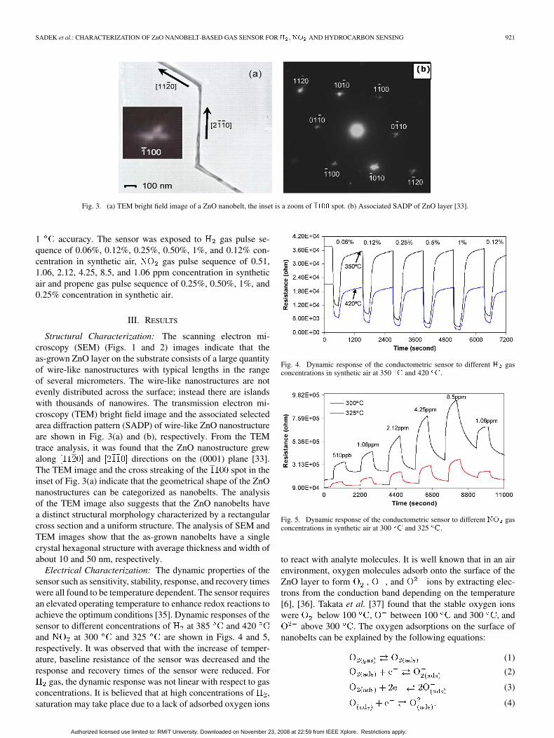
Electrical Characterization: The dynamic properties of thesensor such as sensitivity, stability, response, and recovery timeswere all found to be temperature dependent. The sensor requiresan elevated operating temperature to enhance redox reactions toachieve the optimum conditions [35]. Dynamic responses of thesensor to different concentrations of at 385 and 420and at 300 and 325 are shown in Figs. 4 and 5,respectively. It was observed that with the increase of temper-ature, baseline resistance of the sensor was decreased and theresponse and recovery times of the sensor were reduced. For
gas, the dynamic response was not linear with respect to gasconcentrations. It is believed that at high concentrations of ,saturation may take place due to a lack of adsorbed oxygen ions
Fig. 4. Dynamic response of the conductometric sensor to different H gasconcentrations in synthetic air at 350 C and 420 C.
Fig. 5. Dynamic response of the conductometric sensor to different NO gasconcentrations in synthetic air at 300 C and 325 C.
to react with analyte molecules. It is well known that in an airenvironment, oxygen molecules adsorb onto the surface of theZnO layer to form , , and ions by extracting elec-trons from the conduction band depending on the temperature[6], [36]. Takata et al. [37] found that the stable oxygen ionswere below 100 , between 100 and 300 , and
above 300 . The oxygen adsorptions on the surface ofnanobelts can be explained by the following equations:
(1)
(2)
(3)
(4)
Authorized licensed use limited to: RMIT University. Downloaded on November 23, 2008 at 22:59 from IEEE Xplore. Restrictions apply.

922 IEEE SENSORS JOURNAL, VOL. 7, NO. 6, JUNE 2007
The positively charged ZnO surface and negatively chargedadsorbed oxygen ions form a depletion region at the surface.Since ZnO nanobelts have single crystalline structure with av-erage thickness less than 50 nm (less than Debye length), ad-sorbed oxygen can easily penetrate through the bulk of the belt.As a result, free carriers can travel through the bulk of the beltin a similar way to the channel of a field-effect transistor (FET)[1]. When the device is exposed to a target gas, two differentextremes may occur: pinch-off and fully conductive states. Acomplete depletion of carriers inside the belt will produce apinched-off channel. A complete removal of adsorbed oxygenfrom the belt will produce a highly conductive channel. Whenan n-type ZnO nanobelt surface is exposed to a reducing gassuch as hydrogen or propene at elevated temperatures, analytemolecules dissociate and combine with the adsorbed oxygen,thereby reinjecting electrons. Above 300 , the reactions canbe expressed by the following equations:
(5)
(6)
Due to increase concentration of electrons, the depletion re-gion decreases to produce a conductive channel along the belt,which strongly increases belt conductivity.
In the case of strong oxidizing gas , reactions take placedirectly with the oxide surface rather than with the oxygenchemisorbed at surface. During the interaction process,molecules consume conduction electrons and subsequentlyincrease the depletion region at the surface. Thus, the ZnOnanobelt layer conductivity is reduced after exposure to .The sensor response to can be explained by the followingreactions:
(7)
(8)
The sensitivity of a semiconducting oxide gas sensor is de-fined as follows:
(a) for reducing gas: ;(b) for oxidizing gas: ;
where is the resistance of the sensor in air, is the re-sistance of the sensor in presence of gas.
The sensitivity of the sensor towards and as a func-tion of operating temperature is shown in Fig. 6 and towardspropene in Fig. 7. The sensitivity versus operating temperaturecurve shows a maximum which depends on the target gas. Thiscould be explained by the temperature dependence of the ad-sorption and desorption process on the metal-oxide surface [38].It was observed that the sensitivity towards is highest at220 –250 but other performance parameters such as re-sponse and recovery times are long, repeatability is poor, andthe baseline resistance is not stable. Therefore, the tradeoff be-tween different parameters is needed in choosing the operatingtemperature. Analysis of the experimental results suggest thatthe optimum operating temperatures for the sensor are in therange of 300 –400 for , 300 –350 for , and350 –420 for propene sensing. However, it was found thatthe sensor has the fastest response and recovery with greater re-peatability and baseline stability at operational temperatures of
Fig. 6. Sensitivity versus operating temperature for 1% H and 8.5 ppm NOgas concentrations in synthetic air.
Fig. 7. Sensitivity versus operating temperature for 1% propene concentrationin synthetic air.
Fig. 8. Dynamic response of the conductometric sensor to different H gasconcentrations in synthetic air at 385 C [39].
385 , 350 , and 370 for , , and propene gas, re-spectively. Figs. 8–10 show the dynamic responses of the sensorto different concentrations of at 385 , at 350 ,and propene at 370 , respectively. At these temperatures, thesensitivity of the sensor was calculated to be 14.3 for 1% ,0.81 for 8.5 ppm , and 0.17 for 1% propene. Fast responsetime of 48, 180, 72 s, and recovery time of 336, 268, 252 swere observed for 1% , 1.06 ppm , and 1% propene gas,respectively.
Reproducibility was observed as indicated when a secondpulse of 0.12% , 1.06 ppm , and 0.25% propene wereintroduced into the sensor chamber. It was found that the ZnOnanobelt-based sensor produce repeatable responses of the samemagnitude with good baseline stability.
Authorized licensed use limited to: RMIT University. Downloaded on November 23, 2008 at 22:59 from IEEE Xplore. Restrictions apply.

SADEK et al.: CHARACTERIZATION OF ZnO NANOBELT-BASED GAS SENSOR FOR , AND HYDROCARBON SENSING 923
Fig. 9. Dynamic response of the conductometric sensor to different NO gasconcentrations in synthetic air at 350 C [39].
Fig. 10. Dynamic response of the conductometric sensor to different propenegas concentrations in synthetic air at 370 C.
IV. CONCLUSION
A conductometric gas sensor has been fabricated based onZnO nanobelts synthesized by RF sputtering of a zinc oxidetarget under controlled conditions. Novel gas sensor based onthese ZnO nanobelts has been investigated towards , ,and hydrocarbon at different operating temperatures between150 and 450 . Study shows that the optimum operatingtemperatures for the sensor are in the range of 300 –400for , 300 –350 for , and 350 –420 forpropene sensing. The fastest response and recovery withgreater repeatability for , , and propene gases occurredat 385 , 350 , and 370 , respectively. The resultsdemonstrate that the developed sensors are promising forindustrial applications.
REFERENCES
[1] E. Comini, G. Faglia, G. Sberveglieri, Z. Pan, and Z. L. Wang, “Stableand highly sensitive gas sensors based on semiconducting oxidenanobelts,” Appl. Phys. Lett., vol. 81, pp. 1869–1871, 2002.
[2] D. Kohl, “Surface processes in the detection of reducing gases withSnO -based devices,” Sens. Actuators B, vol. 18, no. 1, pp. 71–113,Jun. 1989.
[3] P. Mitra, A. P. Chatterjee, and H. S. Maiti, “ZnO thin film sensor,” Mat.Lett., vol. 35, pp. 33–38, 1998.
[4] A. A. Tomchenko, G. P. Harmer, and B. T. Marquis, “Detection ofchemical warfare agents using nanostructured metal oxide sensors,”Sens. Actuators B, vol. 108, pp. 41–55, 2005.
[5] T. Seiyama, A. Kato, K. Fujiishi, and M. Nagatani, “A new detector forgaseous components using semiconductive thin films,” Anal. Chem.,vol. 34, pp. 1502–1503, 1962.
[6] P. Esser and W. Gopel, “Physical adsorption on single crystal zincoxide,” Surf. Sci., vol. 97, pp. 309–318, 1980.
[7] S. R. Morrison, Chemical Sensors, in Semiconductor Sensors. NewYork: Wiley, 1994.
[8] G. Barbi, J. Santos, P. Gibson, M. Horrillo, and L. Manes, “Ultrafinegrain-size tin-oxide films for carbon monoxide monitoring in urbanenvironments,” Sens. Actuators B, vol. 24–25, pp. 559–563, 1995.
[9] L. F. Dong, Z. L. Cui, and Z. K. Zhang, “Gas sensing properties ofNano-ZnO prepared by arc plasma method,” NanoStructured Mate-rials, vol. 8, no. 7, pp. 815–823, 1997.
[10] D. Zhang, Z. Liu, C. Li, T. Tang, X. Liu, S. Han, B. Lei, and C. Zhou,“Detection of NO down to ppb levels using individual and multipleIn O nanowire devices,” Nanoletters, vol. 4, no. 10, pp. 1919–1924,2004.
[11] K. M. Sawicka, A. K. Prasad, and P. I. Gouma, “Metal oxide nanowiresfor use in chemical sensing applications,” Sensor Lett., vol. 3, no. 1, pp.1–5, 2005.
[12] H. Y. Dang, J. Wang, and S. S. Fan, “The synthesis of metal oxidenanowires by directly heating metal samples in appropriate oxygen at-mospheres,” Nanotechnology, vol. 14, pp. 738–741, July 2003.
[13] N. Yamazoe, G. Sakai, and K. Shimanoe, “Oxide semiconductor gassensors,” Catal. Surveys Asia, vol. 1, pp. 63–75, 2003.
[14] H. M. Lin, S. Tzeng, P. Hsiau, and W. Tsai, “Electrode effects on gassensing properties of nanocrystalline zinc oxide,” Nanostruct. Mater.,vol. 10, pp. 465–477, 1998.
[15] G. Rao and D. Rao, “Gas sensitivity of ZnO based thick film sensor toNH at room temperature,” Sens. Actuators B, vol. 23, pp. 181–186,1999.
[16] A. P. Chatterjee, P. Mitra, and A. K. Mukhopadhyay, “Chemically de-posited zinc oxide thin film gas sensor,” J. Mater. Sci., vol. 34, pp.4225–4231, 1999.
[17] G. Sberveglieri, P. Nelli, and S. Groppelli, “Oxygen gas sensing char-acteristics at ambient pressure of undoped and lithium-doped ZnO-sputtered thin films,” Mater. Sci. Eng., vol. B7, pp. 63–68, 1990.
[18] B. B. Rao, “Zinc oxide ceramic semiconductor gas sensor for ethanolvapour,” Mater. Chem. Phy., vol. 64, pp. 62–65, 2000.
[19] C. S. Rout, S. Krishna, S. Vivekchand, A. Govindaraj, and C. Rao,“Hydrogen and ethanol sensors based on ZnO nanorods, nanowires andnanotubes,” Chem. Phy. Lett., vol. 418, pp. 586–590, 2006.
[20] S. Si, C. Li, X. Wang, Q. Peng, and Y. Li, “Fe2O3/ZnO core-shellnanorods for gas sensors,” Sens. Actuators B, 2006, to be published.
[21] Z. L. Wang, “Nanostructures of zinc oxide,” Materialstoday, vol. 7, no.6, pp. 26–33, 2004.
[22] T. H. Wang, B. Kang, F. Ren, L. Tien, P. Sadik, and D. Norton, “Hy-drogen-selective sensing at room temperature with ZnO nanorods,”Appl. Phy. Lett., vol. 86, pp. 1–3, 2005.
[23] C. Xiangfeng, J. Dongli, A. Djurisic, and Y. Leung, “Gas-sensing prop-erties of thick film based on ZnO nano-tetrapods,” Chem. Phy. Lett.,vol. 401, pp. 426–429, 2005.
[24] C. Baratto, G. Sberveglieri, A. Onischuk, B. Caruso, and S. di Stasio,“Low temperature selective NO2 sensors by nanostructured fibers ofZnO,” Sens. Actuators B, vol. 100, pp. 261–265, 2004.
[25] Y. Zhang, K. Yu, D. Jiang, Z. Zhu, H. Geng, and L. Luo, “Zinc oxidenanorod and nanowire for humidity sensor,” Appl. Surf. Sci., vol. 242,pp. 212–217, 2005.
[26] M. K. Hossain, S. C. Ghosh, Y. Boontongkong, C. Thanachayanont, andJ. Dutta, “Growth of zinc oxide nanowires and nanobelts for gas sensingapplications,” J. Metastable Nanocrys. Mater., vol. 23, pp. 27–30, 2005.
[27] S. Kang, Y. Heo, C. Tien, P. Norton, F. Ren, B. Gila, and S. Pearton,“Hydrogen and ozone gas sensing using multiple ZnO nanorods,” Appl.Phy. A: Mater. Sci. Proces., vol. 80, pp. 1029–1032, 2005.
[28] P. X. Gao, C. S. Lao, W. L. Hughes, and Z. L. Wang, “Three-dimen-tional interconnected nanowire networks of ZnO,” Chem. Phy. Lett.,vol. 408, pp. 174–178, 2005.
[29] S. Choopun, H. Tabata, and T. Kawai, “Self-assembly ZnO nanorodsby pulsed laser deposition under argon atmosphere,” J. Cryst. Growth,vol. 274, pp. 167–172, 2005.
[30] W. I. Park, D. H. Kim, S.-W. Jung, and G.-C. Yi, “Metal-organic vapor-phase epitaxial growth of vertically well-aligned ZnO nanorods,” Appl.Phys. Lett., vol. 80, pp. 4232–4235, 2002.
[31] Z. W. Pan, Z. R. Dai, and Z. L. Wang, “Nanobelts of semiconductingoxides,” Science, vol. 291, pp. 1947–1949, 2001.
[32] W. T. Chiou, W. Y. Wu, and J. M. Ting, “Growth of single crystal ZnOnanowires using sputter deposition,” Diamond Related Mater., vol. 12,pp. 1841–1844, 2003.
[33] S. Choopun, N. Hongsith, S. Tanunchai, T. Chairuangsri, C. Kruain,S. Singkarat, T. Vilaithong, P. Mangkorntong, and N. Mangkorntong,“Single crystalline ZnO nanobelts by RF sputtering,” J. Crys. Growth,vol. 282, pp. 365–369, 2005.
[34] D. L. Smith, Thin-Film Deposition: Principles and Practice. NewYork: McGraw-Hill, 1995.
Authorized licensed use limited to: RMIT University. Downloaded on November 23, 2008 at 22:59 from IEEE Xplore. Restrictions apply.

924 IEEE SENSORS JOURNAL, VOL. 7, NO. 6, JUNE 2007
[35] C. Yu, Q. Hao, S. Saha, L. Shi, X. Kong, and Z. L. Wang, “Integrationof metal oxide nanobelts with microsystems for nerve agent detection,”Appl. Phy. Lett., vol. 86, pp. 063101–063103, 2005.
[36] D. M. Wilson, S. Hoyt, J. Janata, K. Booksh, and L. Obando, “Chemicalsensors for portable, handheld field instruments,” IEEE Sensors J., vol.1, no. 4, pp. 256–274, Dec. 2001.
[37] M. Takata, D. Tsubone, and H. Yanagida, “Dependance of electricalconductivity of ZnO on degree of sensing,” J. Amer. Ceram. Soc., vol.59, pp. 4–8, 1976.
[38] Y. Wang, X. Wu, Y. Li, and Z. Zhou, “Mesostructured SnO assensing materials for gas sensors,” Solid-State Elec., vol. 48, pp.627–632, 2004.
[39] A. Z. Sadek, W. Wlodarski, K. Kalantar-zadeh, and S. Choopun, “ZnOnanobelt based conductometric H and NO gas sensors,” in Proc.IEEE Sensors Conf., 2005, pp. 1326–1329.
Abu Z. Sadek (S’06) received the B.Sc. degreein electrical and electronics engineering from theBangladesh University of Engineering and Tech-nology (BUET), Dhaka, Bangladesh, in 1998 andthe M.E. degree in telecommunications engineeringfrom the University of Melbourne, Melbourne, Aus-tralia, in 2002. He is currently working towards thePh.D. degree at the Sensor Technology Laboratory,School of Electrical and Computer Engineering,RMIT University, Melbourne.
His research interests include chemical and bio-chemical sensors, micro and nanotechnology, acoustic propagation, and con-ducting polymers.
Supab Choopun received the Ph.D. in chemicalphysics from University of Maryland, College Park,in 2002.
Currently, he is an Instructor at the Department ofPhysics, Faculty of Science, Chiang Mai University,Chiang Mai, Thailand. His current research interestsare in the field of metal-oxide semiconductor nanos-tructures such as ZnO for gas sensor and solar cellapplications.
Wojtek Wlodarski (M’72) has worked in the areasof sensor technology and instrumentation for over30 years. He has published four books and mono-graphs, over 400 papers, and holds 29 patents. He is aProfessor at RMIT University, Melbourne, Australia,and heads the Sensor Technology Laboratory at theSchool of Electrical and Computer Engineering.
Samuel J. Ippolito received the B.Eng. degree incomputer systems engineering (Hon) from RMITUniversity, Melbourne, Australia, in 2002. He iscurrently working towards the Ph.D. degree in sensortechnology at RMIT University.
His major research interest areas include mod-eling, fabrication and application of layeredSAW-based chemical sensors based on thin-filmtechnology.
Kourosh Kalantar-zadeh (M’94) is a TenuredAcademic at the School of Electrical and Com-puter Engineering, RMIT University, Melbourne,Australia. He has published more than 80 scientificpapers in the refereed journals and in the proceed-ings of international conferences. He holds threepatents. He is currently authoring a book entitledNanotechnology Enabled Sensors. His researchinterests include chemical and biochemical sensors,nanotechnology, MEMS, thermoelectric materials,electronic circuits, and micro-fluidics.
Authorized licensed use limited to: RMIT University. Downloaded on November 23, 2008 at 22:59 from IEEE Xplore. Restrictions apply.