IEEE JOURNAL OF SOLID-STATE CIRCUITS, VOL. 49, …IEEE JOURNAL OF SOLID-STATE CIRCUITS, VOL. 49, NO....
16
IEEE JOURNAL OF SOLID-STATE CIRCUITS, VOL. 49, NO. 10, OCTOBER 2014 2243 A 5 Gb/s, 10 ns Power-On-Time, 36 W Off-State Power, Fast Power-On Transmitter for Energy Proportional Links Tejasvi Anand, Student Member, IEEE, Amr Elshazly, Member, IEEE, Mrunmay Talegaonkar, Student Member, IEEE, Brian Young, Student Member, IEEE, and Pavan Kumar Hanumolu, Member, IEEE Abstract—A fast power-on transmitter architecture that enables energy proportional communication for server and mobile plat- forms is presented. The proposed architecture and circuit tech- niques achieve fast power-on capability in voltage mode output driver by using fast-digital regulator, and in the clock multiplier by accurate frequency pre-setting and periodic reference insertion. To ease timing requirements, an improved edge replacement logic circuit for the clock multiplier is proposed. The proposed trans- mitter demonstrates energy proportional operation over wide vari- ations of link utilization, and is therefore suitable for energy effi- cient links. Fabricated in 90 nm CMOS technology, the voltage mode driver and the clock multiplier achieve power-on-time of only 2 ns and 10 ns, respectively. By using highly scalable digital architecture with accurate frequency pre-setting and instantaneous phase acquisi- tion, the prototype MDLL-based clock multiplier achieves 10 ns (3 reference cycles) power-on-time, 2 ps long-term absolute jitter at 2.5 GHz output frequency. The proposed fast power-on trans- mitter architecture consumes 4.8 mW/36 W on/off-state power from 1.1 V supply, has 10 ns total power-on time, and achieves 100 effective data rate scaling (5 Gb/s-0.048 Gb/s), while scaling the power and energy efficiency by only 50 (4.8 mW–0.095 mW) and 2 (1–2 pJ/Bit), respectively. The proposed transmitter occu- pies an active die area of 0.3 mm . Index Terms—Burst mode, digital regulator, energy efficient, en- ergy proportional, fast power-on, I/O, multiplying delay locked loop (MDLL), serial link, transmitter. I. INTRODUCTION E VER-INCREASING demand for higher bandwidth in mobile devices and high performance servers has been the main driving force behind energy efficient links. Innovation Manuscript received November 27, 2013; revised June 15, 2014; accepted July 21, 2014. Date of publication August 28, 2014; date of current version September 22, 2014. This paper was approved by Associate Editor Jack Kenney. This work was supported in part by the Intel Labs University Research Office, SRC under task ID:1836.125, 1836.129, and the National Science Foundation under CAREER EECS-0954969. T. Anand, M. Talegaonkar, and P. K. Hanumolu are with the Department of Electrical and Computer Engineering, University of Illinois at Urbana-Cham- paign, Urbana, IL 61801 USA (e-mail: [email protected]). A. Elshazly is with Intel Corporation, Hillsboro, OR 97124 USA. B. Young is with Marvell, Corvallis, OR 97333 USA. Color versions of one or more of the figures in this paper are available online at http://ieeexplore.ieee.org. Digital Object Identifier 10.1109/JSSC.2014.2345764 in circuit and signaling techniques together with voltage and process scaling enabled almost 15% energy efficiency improve- ment each year over the past decade. However, despite this achievement, with the ongoing push to achieve data through- puts in the 1 TB/s range, the serial link power is becoming unacceptably large. Further increase in the data rates is limited by the thermal constraints of the package [1]. Therefore, in order to push the bandwidth without hitting the power wall, a paradigm shift in the design of serial links is needed. A serial link in applications such as a memory controller or an Ethernet interface is used only when there is a request to ac- cess memory due to a miss in the last level cache or a request to download a web page. Thus, instantaneous bandwidth demand (utilization) of the link varies over time. As shown in Fig. 1(a), when a conventional link is idle, it consumes idle power, which is a significant portion of the total operating power. As a re- sult, energy efficiency of such link, as quantified by the energy- per-bit metric, degrades when the link utilization is low. Tech- niques such as dynamic power management [2], [3] achieve significant power saving by scaling the supply voltage to meet the link bandwidth demand. However, any change in the link rate requires dropping the existing link and re-negotiating new data rates between transmitter and receiver, which is time con- suming. Moreover, these techniques offer only limited link rate scaling. In view of these drawbacks, power-cycling or burst-mode communication where a link is powered-on only when needed has recently emerged as an attractive means to scale the link power based on its utilization levels [4]–[8]. In these systems, the link is powered down when idle and powered back up in- stantaneously when data is ready to be transferred, resulting in the most energy efficient use of link bandwidth. In such system, the power consumption scales linearly with link utilization, re- sulting in energy consumption to become proportional to the transferred data, as shown in Fig. 1(b). This mode of operation is commonly referred to as energy proportional operation [9]. In these energy proportional links (EPL), the energy-per-bit of the link stays constant across all utilization levels (see Fig. 1(b)) and is achieved without compromising their active link power. For example, serial interface with 5 ns fast power-on receiver [6] achieves 1.4 pJ/bit energy efficiency. 0018-9200 © 2014 IEEE. Personal use is permitted, but republication/redistribution requires IEEE permission. See http://www.ieee.org/publications_standards/publications/rights/index.html for more information.
Transcript of IEEE JOURNAL OF SOLID-STATE CIRCUITS, VOL. 49, …IEEE JOURNAL OF SOLID-STATE CIRCUITS, VOL. 49, NO....

IEEE JOURNAL OF SOLID-STATE CIRCUITS, VOL. 49, NO. 10, OCTOBER 2014 2243
A 5 Gb/s, 10 ns Power-On-Time, 36 WOff-State Power, Fast Power-On Transmitter
for Energy Proportional LinksTejasvi Anand, Student Member, IEEE, Amr Elshazly, Member, IEEE,
Mrunmay Talegaonkar, Student Member, IEEE, Brian Young, Student Member, IEEE, andPavan Kumar Hanumolu, Member, IEEE
Abstract—A fast power-on transmitter architecture that enablesenergy proportional communication for server and mobile plat-forms is presented. The proposed architecture and circuit tech-niques achieve fast power-on capability in voltage mode outputdriver by using fast-digital regulator, and in the clock multiplierby accurate frequency pre-setting and periodic reference insertion.To ease timing requirements, an improved edge replacement logiccircuit for the clock multiplier is proposed. The proposed trans-mitter demonstrates energy proportional operation over wide vari-ations of link utilization, and is therefore suitable for energy effi-cient links.Fabricated in 90 nm CMOS technology, the voltage mode driver
and the clock multiplier achieve power-on-time of only 2 ns and 10ns, respectively. By using highly scalable digital architecture withaccurate frequency pre-setting and instantaneous phase acquisi-tion, the prototype MDLL-based clock multiplier achieves 10 ns (3reference cycles) power-on-time, 2 ps long-term absolute jitterat 2.5 GHz output frequency. The proposed fast power-on trans-mitter architecture consumes 4.8 mW/36 W on/off-state powerfrom 1.1 V supply, has 10 ns total power-on time, and achieves100 effective data rate scaling (5 Gb/s-0.048 Gb/s), while scalingthe power and energy efficiency by only 50 (4.8 mW–0.095 mW)and 2 (1–2 pJ/Bit), respectively. The proposed transmitter occu-pies an active die area of 0.3 mm .
Index Terms—Burst mode, digital regulator, energy efficient, en-ergy proportional, fast power-on, I/O, multiplying delay lockedloop (MDLL), serial link, transmitter.
I. INTRODUCTION
E VER-INCREASING demand for higher bandwidth inmobile devices and high performance servers has been
the main driving force behind energy efficient links. Innovation
Manuscript received November 27, 2013; revised June 15, 2014; acceptedJuly 21, 2014. Date of publication August 28, 2014; date of current versionSeptember 22, 2014. This paper was approved byAssociate Editor Jack Kenney.This work was supported in part by the Intel Labs University Research Office,SRC under task ID:1836.125, 1836.129, and the National Science Foundationunder CAREER EECS-0954969.T. Anand, M. Talegaonkar, and P. K. Hanumolu are with the Department of
Electrical and Computer Engineering, University of Illinois at Urbana-Cham-paign, Urbana, IL 61801 USA (e-mail: [email protected]).A. Elshazly is with Intel Corporation, Hillsboro, OR 97124 USA.B. Young is with Marvell, Corvallis, OR 97333 USA.Color versions of one or more of the figures in this paper are available online
at http://ieeexplore.ieee.org.Digital Object Identifier 10.1109/JSSC.2014.2345764
in circuit and signaling techniques together with voltage andprocess scaling enabled almost 15% energy efficiency improve-ment each year over the past decade. However, despite thisachievement, with the ongoing push to achieve data through-puts in the 1 TB/s range, the serial link power is becomingunacceptably large. Further increase in the data rates is limitedby the thermal constraints of the package [1]. Therefore, inorder to push the bandwidth without hitting the power wall, aparadigm shift in the design of serial links is needed.A serial link in applications such as a memory controller or
an Ethernet interface is used only when there is a request to ac-cess memory due to a miss in the last level cache or a request todownload a web page. Thus, instantaneous bandwidth demand(utilization) of the link varies over time. As shown in Fig. 1(a),when a conventional link is idle, it consumes idle power, whichis a significant portion of the total operating power. As a re-sult, energy efficiency of such link, as quantified by the energy-per-bit metric, degrades when the link utilization is low. Tech-niques such as dynamic power management [2], [3] achievesignificant power saving by scaling the supply voltage to meetthe link bandwidth demand. However, any change in the linkrate requires dropping the existing link and re-negotiating newdata rates between transmitter and receiver, which is time con-suming. Moreover, these techniques offer only limited link ratescaling.In view of these drawbacks, power-cycling or burst-mode
communication where a link is powered-on only when neededhas recently emerged as an attractive means to scale the linkpower based on its utilization levels [4]–[8]. In these systems,the link is powered down when idle and powered back up in-stantaneously when data is ready to be transferred, resulting inthe most energy efficient use of link bandwidth. In such system,the power consumption scales linearly with link utilization, re-sulting in energy consumption to become proportional to thetransferred data, as shown in Fig. 1(b). This mode of operationis commonly referred to as energy proportional operation [9].In these energy proportional links (EPL), the energy-per-bit ofthe link stays constant across all utilization levels (see Fig. 1(b))and is achieved without compromising their active link power.For example, serial interface with 5 ns fast power-on receiver[6] achieves 1.4 pJ/bit energy efficiency.
0018-9200 © 2014 IEEE. Personal use is permitted, but republication/redistribution requires IEEE permission.See http://www.ieee.org/publications_standards/publications/rights/index.html for more information.

2244 IEEE JOURNAL OF SOLID-STATE CIRCUITS, VOL. 49, NO. 10, OCTOBER 2014
Fig. 1. Bandwidth availability, usage scenarios together with power consumption and energy-per-bit. (a) Conventional link. (b) Proposed energy proportional link(EPL).
In order to achieve such performance, these links need tobe powered on/off in no time, consume near zero power in theoff-state, and incur minimum energy overhead during on-to-offand off-to-on state transitions. In practice, it is very difficult tomeet these requirements. Phase locking the clock multiplier onpower-on and bringing voltage regulator to a steady state aresome of the big challenges in achieving these goals.In this paper, we present a fast power-on transmitter con-
sisting of a voltage mode driver and a clock multiplier.Fabricated in 90 nm CMOS process, the prototype transmitterachieves 100 effective data rate range (5 Gb/s–0.048 Gb/s)while scaling the power by 50 (4.8 mW–0.095 mW) andenergy efficiency by only 2 (1–2 pJ/Bit). Such energy propor-tional operation is achieved by using a fast power-on voltagemode driver and multiplying delay locked loop (MDLL) baseddigital clock multiplier. In this work, wide effective data raterange is achieved by duty cycling the transmitter at a fixeddata rate of 5 Gb/s and not by changing active data rate. Byadopting a digital voltage regulator, the prototype voltagemode driver achieves 2 ns power-on time, less than 11 Woff-state power, 32 pJ energy overhead for on/off transition,and 2.6 mW on-state power at 5 Gb/s output data rate. Byemploying a highly scalable digital architecture with accuratefrequency pre-setting and instantaneous phase acquisition, theprototype 8 /16 clock multiplier achieves 10 ns (3 referencecycles) power-on time, 2 ps long-term absolute jitter, lessthan 25 W off-state power, 12 pJ energy overhead for on/offtransition, and 2.2 mW on-state power at 2.5 GHz outputfrequency [10].The rest of the paper is organized as follows. Section II dis-
cusses the effect of circuit non-idealities on the energy pro-portional behavior of links. Section III discusses the buildingblocks of a conventional transmitter and their limitations forenergy proportional link application. Section IV introduces theproposed transmitter architecture. Circuit details of the clockmultiplier are discussed in Section V. Section VI presents themeasured results. Section VII concludes the paper.
II. EFFECT OF NON-IDEALITIES ON ENERGYPROPORTIONAL LINKS
Practical energy proportional links have finite power-on time,non-zero off-state power, and finite power-cycling energy. Ef-fect of these parameters on the link’s energy efficiency (en-ergy-per-bit) can be mathematically captured as:
(1)
where is the on-state power, is the off-statepower, is the on-state time, is the off-state time,
is the power-on time and is theenergy consumed during on/off transition.Finite power-on time is due to the time required to charge/dis-
charge bias nodes, and time needed for the clock multiplierto achieve frequency and phase lock. Assuming the link con-sumes approximately peak power during power-on transition,this wasted energy equates to . The effectof power-on time on link efficiency is shown in Fig. 2(a). Fora constant burst length, power-on energyincreases the energy-per-bit by a fixed amount across all linkutilization values.Fig. 2(b) illustrates the effect of static off-state power on link
energy-efficiency. At lower link utilization ,even with a small off-state power , the off-state energy
starts to dominate link energy-efficiency. There-fore, the off-state power must be close to zero to achieve con-stant energy-per-bit at extremely low data rates.Power-cycling energy is the energy consumed in charging/
discharging nodes in each power cycle or data burst event.Therefore, more frequent data bursts incur larger energypenalty. Fig. 2(c) shows the effect of burst length on en-ergy-per-bit for a fixed effective data rate. When the data istransferred in smaller bursts, energy spent in powering-on

ANAND et al.: A 5 Gb/s, 10 ns POWER-ON-TIME, 36 W OFF-STATE POWER, FAST POWER-ON TRANSMITTER FOR ENERGY PROPORTIONAL LINKS 2245
Fig. 2. (a) Effect of power-on time on link energy efficiency. (b) Effect of static off-state power on link energy efficiency. (c) Effect of data burst length on linkenergy efficiency.
the link and power cycling energybecomes comparable to the on-state energy
and consequently leads to increased energy-per-bit.Plot of energy-per-bit versus utilization captures most essen-
tial features of energy proportional links. With the help of thisplot, energy consumption estimates can be made for a given linkusage scenario of an application. Thus, it forms one of the im-portant metrics to characterize and compare such links.
III. LIMITATIONS OF CONVENTIONAL TRANSMITTER FOR USEIN ENERGY PROPORTIONAL LINKS
A. Output Driver
Voltage-mode (VM) drivers dissipate a quarter of the poweras compared to the current-mode logic (CML) output drivers[11]. However, voltage regulators required to set output swingand termination impedance cannot be powered-on instanta-neously. Keeping these regulators always-on, severely impactsenergy-per-bit at lower data rates [5]. Digital voltage regulators[12], [13], provide a means to power-on/off rapidly whileconsuming no static power in the off-state. Pass transistor in the
digital regulator also helps in power-gating the logic, resultingin low leakage power in the off-state. For these reasons, digitalregulators are employed in the proposed VM driver.
B. Clock Multiplier
The long locking time of conventional clock multipliersimplemented using phase-locked loops (PLLs) presents thebiggest bottleneck in achieving energy proportional operation.Increasing the PLL bandwidth reduces the locking time. How-ever, to ensure loop stability, loop bandwidth cannot exceedone tenth the reference frequency [14]. As a result, even ifthe VCO frequency is precisely set digitally, the sluggishphase acquisition limits the phase locking time to at best fewhundred nanoseconds [5], [15]. Techniques such as dynamicphase error compensation [16], edge-missing compensation[17], and hybrid PLLs [18] improve the phase acquisition time.By calibrating the phase of the feedback clock, best power-ontime of forty reference cycles has also been reported [19].However, such improvements are inadequate to achieve energyproportional operation goal.

2246 IEEE JOURNAL OF SOLID-STATE CIRCUITS, VOL. 49, NO. 10, OCTOBER 2014
Fig. 3. Schematic diagram of the proposed fast power-on transmitter.
Multiplying injection locked oscillator (MILO) provides ameans to reduce power-on time. By increasing MILO’s band-width with stronger injection strength, the locking time can bereduced. However, a wide bandwidth results in large spurs atthe injection frequency [20]. Filtering of MILO’s output witha second injection locked oscillator (ILO) could reduce thesespurs. However, it comes at the cost of extra power [21].Multiplying delay locked loop (MDLL) provides a means
to overcome the drawbacks of MILOs. In MDLL, every thVCO edge is replaced by the clean reference edge by openingup the ring oscillator for a brief period using a narrow pulse[22]–[24]. This edge replacement results in instantaneous phaselocking, which is independent of the bandwidth. Inserting aclean reference edge every reference cycle resets all accumu-lated jitter in the VCO and results in superior jitter performance[25], [26]. These features make MDLL a suitable candidate forfast power-on applications.
IV. PROPOSED FAST POWER-ON TRANSMITTER ARCHITECTURE
Fig. 3 shows the block diagram of the proposed transmitter.It consists of a fast power-on clock multiplier, a 2:1 latch-basedmultiplexer, and a voltage mode driver output stage. Theclock multiplier, implemented using a digital multiplyingdelay-locked loop (MDLL), generates a 2.5 GHz output from a312.5 MHz reference clock. The PRBS9 generator outputs dataat 2.5 Gb/s, which is serialized and transmitted at 5 Gb/s with250 mV differential peak-to-peak output swing.The proposed voltage mode driver consists of a replica bias,
pre-driver, and output driver. The replica bias circuit generatesreference voltages and for the pre-driverand output driver regulators, respectively. neededto create 50 ohm output impedance is generated by enclosing
a replica of the output driver [27], which is 1/16th the originalsize, in a closed loop. sets the differential output driverswing. Pre-driver and output driver regulators use the replicabias output to generate virtual supply voltages for the pre-driver
and output driver , respectively. These regula-tors are implemented using digital feedback loops, which help instoring states during power-off event and restoring them duringpower-on.Fig. 4 shows the schematic of the proposed voltage regulator.
It consists of a clocked comparator, an accumulator, and a resis-tive DAC. is compared with and the output is fedto the 12 bit accumulator. The accumulated output drives a 7 bitresistive DAC to minimize error between and . Thelower 5-LSBs of the accumulator output are ignored to reducevoltage ripple due to loop delay. A 20 pF decoupling capacitorat the output of transistor helps in suppressing noise on theoutput voltage.
A. Power-On Transient Response of the Transmitter
Fig. 5 shows the transient response of the transmitter. Whenthe signal is de-asserted, the pre-driver and outputdriver regulator output and nodes are dischargedto ground. The gates of transistors and are pulled low(see Fig. 3), the clock to all comparators is gated and bias cur-rent of the replica bias block is turned off. In this state, only theleakage current in digital logic contributes to off-state powerconsumption. During the off-state, regulator states are saved intheir respective accumulators.When the signal is asserted, the DACs rapidly re-
store the accumulator’s state and set the gate voltages of transis-tors and , which quickly bring and to thedesired value. The 20 pF decoupling capacitor charges up in 2 nsafter which the driver is ready for transmitting data. The MDLL

ANAND et al.: A 5 Gb/s, 10 ns POWER-ON-TIME, 36 W OFF-STATE POWER, FAST POWER-ON TRANSMITTER FOR ENERGY PROPORTIONAL LINKS 2247
Fig. 4. Schematic diagram of the proposed digital voltage regulator.
Fig. 5. Transient response of the proposed fast power-on transmitter.
based clockmultiplier limits the transmitter start-up time, whichtakes around 10 ns (3 reference cycles) to start.
B. Effect of Power Supply Droop on Output Driver
Burst mode operation requires fast load transient responselinear regulators [28]–[30] to power the transmitter. When theoutput driver is powered-on, output of the regulator droops mo-mentarily before regaining its original value. The amount ofdroop and transient response time are a function of loop dy-namics of external regulator and current step. In order to capturethis effect, output driver including the multiplexer is simulatedwith a fast load transient response regulator. Fig. 6 shows thecurrent step, power-supply droop and the output eye diagramat various time instants. Droop in the power supply increasesoutput jitter which will eventually reduce the sampling marginon the receiver.
C. Fast Power-On Clock Multiplier
Fig. 7 shows the block diagram of the proposed MDLLbased digital clock multiplier. It employs a split tuned archi-tecture in which a frequency locked loop (FLL) drives the ringoscillator close to frequency lock, and an integral control thatbrings oscillator frequency to the desired output frequency. Theproportional path ensures stability by periodically resetting theoscillator output phase with the input reference clock phaseusing edge replacement logic (ERL). Frequency locked loopconsists of a frequency detector, 12 bit accumulator clockedat , fast settling DAC and constant current source. Integral path uses a bang-bang phase detector, 13 bit ac-
cumulator, and 8 bit DAC. The phase detector consisting oftwo D flip-flops, clocked at the reference frequency, produceslead/lag phase information with a 1 bit output. The accumulatorclocked at integrates the sub-sampled bang-bangphase detector output.The proportional path consists of a programmable divider and
edge replacement logic (ERL). The edge replacement logic gen-erates a narrow signal pulse, which opens up the ring oscil-lator momentarily and passes the clean reference edge. In orderto have a perfect edge replacement, care is taken to generate the
signal with sharp rise and fall times.The digital accumulators store the frequency information of
the oscillator in the digital form during the power-off state. Theyare synthesized with high devices to reduce leakage. FourLSBs from the frequency locked loop accumulator and 5 LSBsfrom the fine integral path accumulator are ignored to avoidripple on control voltage node, , due to loop delay. Inorder to reduce the power-on time penalty caused by slow set-tling transients, the DAC bias circuitry is not turned-off in thepower-off state. The bias voltages are maintained at the expenseof small power penalty during the off-state. When the MDLLis powered-on, the frequency information is rapidly restored tothe oscillator using fast Nyquist-rate DACs, thus bringing theoscillator to frequency lock quickly. Once frequency lock isachieved, the rising edge of the reference replaces the th os-cillator edge thus achieving instantaneous phase lock.Periodic edge replacement results in current being drawn pe-
riodically from , thereby causing a supply ripple at ref-erence frequency and its harmonics. Despite the pseudo differ-

2248 IEEE JOURNAL OF SOLID-STATE CIRCUITS, VOL. 49, NO. 10, OCTOBER 2014
Fig. 6. Simulated power supply droop on the output driver.
Fig. 7. Schematic diagram of the proposed fast power-on MDLL based digital clock multiplier.
ential nature of VCO, current drawn by VCO is not constant,which causes ripple on . Deterministic jitter (DJ) re-sulting from ripple can be reduced with a decouplingcapacitor. However, a large decoupling capacitor increases thetime constant on the node, thereby increasing the time ittakes for the frequency to settle to the right value, which eventu-ally increases power-on time. In order to quantify this trade-off
between DJ and power-on time, a bank of programmable decou-pling capacitor ( bank) is added on the node and themeasured results are presented in Section VI.
D. Power-On Transient Response of the Clock Multiplier
Fig. 8 shows the power-on transient response of the proposedclock multiplier. When the multiplier is powered-off,

ANAND et al.: A 5 Gb/s, 10 ns POWER-ON-TIME, 36 W OFF-STATE POWER, FAST POWER-ON TRANSMITTER FOR ENERGY PROPORTIONAL LINKS 2249
Fig. 8. Transient response of the proposed fast power-on clock multiplier.
Fig. 9. Schematic diagram of the voltage-controlled oscillator.
signal is gated, signal is asserted high and the VCOstops oscillating. Once the VCO is open, it no longer sinkscurrent. This causes node to charge up to , whicheventually shuts down current source . When the multiplier ispowered-on, the signal is de-asserted, and the VCO startsto oscillate. The node then settles to the desired valuewith a finite time constant. During the time when nodeis settling, the VCO oscillates at a higher frequency, whichcauses the rising edge of the divider output signalto appear earlier than desired. On rising edge of thesignal, signal is asserted high, and the VCO opens up andwaits for the rising edge of the signal to pass through.During this wait period, VCO stops and the nodeagain rises towards . On the subsequent rising edge of thereference, the SEL signal is de-asserted, and the VCO beginsto oscillate again.
In the second reference cycle, node again settles tothe desired value but the initial high oscillation frequency againcauses rising edge of the divider output signal to ap-pear earlier than desired. However, this time it appears closer tothe rising edge of reference signal, which causes smaller distur-bance on the node. In the third reference cycle, distur-bance on the node is even smaller and the multiplier isclose to achieving frequency and phase lock. Thus, in the pro-posed MDLL architecture, the power-on time is mainly limitedby the time constant on the node.
V. CLOCK MULTIPLIER BUILDING BLOCKS
A. Voltage Controlled Oscillator (VCO)
Schematic diagram of VCO is shown in Fig. 9. It consists offive stages connected in a ring configuration. One of these five

2250 IEEE JOURNAL OF SOLID-STATE CIRCUITS, VOL. 49, NO. 10, OCTOBER 2014
Fig. 10. Simulated power supply induced jitter (PSIJ) of VCO (includingDAC) and MDLL.
stages is an inverting multiplexer and the rest four are cross cou-pled inverters. signal is tapped from themiddleof the VCO. This signal is used to meet timing requirements inthe edge replacement logic. signal to the multiplexer isdriven by a VCO delay cell, shown as a shaded cell in Fig. 9.Passing the signal through the VCO buffer matches therise time of edge with edge resulting in lowerreference spur at the output. Choice of five stages in the oscil-lator was made carefully to achieve sharp rise and fall times,which helps in reducing deterministic jitter caused due to im-perfect reference edge replacement. Resistive cross couplingon the multiplexer was avoided to reduce noise coupling from
edge to the clean edge during the edge replace-ment operation. Choice of pseudo differential stages was madeto achieve smaller self induced ripple on the node, re-sulting in better jitter performance with a smaller decouplingcapacitor. When simulated at 2.5 GHz, the VCO consumes ap-proximately 550 A from a 1.1 V supply.Power supply induced jitter (PSIJ) of the VCO (including
DACs) and MDLL is a strong function of decoupling capac-itor on the node. Simulated value for
pF and 20 pF is shown in Fig. 10. At 100 MHz sinu-soidal supply disturbance, simulated of MDLL for
pF and 20 pF is 2 ps/mV and 0.053 ps/mV respectively.At 1MHz sinusoidal supply disturbance, simulatedof MDLL for pF and 20 pF is 0.43 ps/mV.
B. Edge Replacement Logic (ERL)
Edge replacement logic is responsible for generating a narrowpulse to pass the clean reference edge every th VCO cycle.The width of this pulse is typically . Conventional se-lect logic requires synchronous thermometric counter running atVCO frequency to generate periodic pulses of one VCO periodwidth [22]. However, running a synchronous counter at VCOfrequency results in large power dissipation. Moreover, the ini-tial VCO frequency is required to be higher than ,which limits this circuit [22] to be used for fast power-on appli-cations where the VCO frequency is very close toduring power-on.During normal operation, the SEL signal must be de-asserted
after the rising edge of REF signal and before the falling edge
of the VCO output, and within time in the best case.The select logic in [26] avoids thermometric counter, but suffersfrom timing constraint, which is difficult to meetat higher VCO frequencies. In this work, the proposed ERL em-ploys ripple counter to reduce power consumption, and uses ad-vanced reference signal to overcome the timingconstraint.Fig. 11 shows the schematic and timing diagram of the pro-
posed ERL circuit. When the signal is low, the outputof the first stage, is pre-charged to logic high. Afterthe completion of VCO cycles, the signal is as-serted high. The signal is asserted high on the falling edgeof . The signal opens up the oscillatorand waits for the rising edge to pass. signalis generated by tapping the signal before the delayed
goes into the VCO. On the rising edge of the ,output of Stage1 is discharged and signal is de-asserted.The timing by which the signal must be advancedwith-respect-to signal is given by the following equation:
(2)
where is the time between risingedge to falling edge.
C. DAC
Delta-sigma DACs followed by post filter offer a compactway to achieve high-resolution frequency control of the VCOs.However, large time constant of the post-filter increases thefrequency settling time. The proposed Nyquist-rate DAC andits timing diagram is shown in Fig. 12. The DAC is imple-mented using thermometer-coded current-mode architectureto ensure monotonicity and fast settling. Single ended sourceswitched PMOS current elements are used to minimize area. Byemploying current mode Nyquist-rate DACs, use of low band-width post-filter is avoided, thereby achieving high bandwidthto rapidly set VCO frequency during power-on/off events.When the system is powered-off, clock to the accumulator isgated and accumulator holds its state. De-asserting thesignal causes the output of binary to thermometric logic to godown to zero, which shuts down the DAC. When the system ispowered-on, previous state of the DAC is restored andquickly reaches the desired value.The choice of DAC’s resolution and frequency tuning range is
governed by tolerable frequency quantization error. Frequencyquantization error results in accumulation of VCO phase for onereference cycle, which results in deterministic jitter and conse-quently reference spurs. For a given DAC resolution and fre-quency tuning range, deterministic jitter can be estimatedmathematically as follows:
(3)
where is the frequency tuning range, is the frequencymultiplication factor, is the size of DAC,is the VCO frequency, and is the VCO period. Using(3), plot of deterministic jitter as a function of frequency tuning

ANAND et al.: A 5 Gb/s, 10 ns POWER-ON-TIME, 36 W OFF-STATE POWER, FAST POWER-ON TRANSMITTER FOR ENERGY PROPORTIONAL LINKS 2251
Fig. 11. Schematic and timing diagram of the proposed edge replacement logic (ERL).
Fig. 12. Schematic and timing diagram of the Nyquist-rate DAC.
Fig. 13. Simulated deterministic jitter as a function of frequency tuning rangefor and GHz.
range for various DAC sizes is shown in Fig. 13. Increasing theDAC resolution on one-hand reduces the frequency quantiza-tion error and on the other-hand increases the area and para-sitic capacitance on the (virtual supply node of VCO),which eventually increases the power-on time of MDLL. De-sign of fast power-on MDLL with wide frequency tuning rangeVCO remains a challenging problem. In the proposed architec-ture, 8 bit integral path DAC provides up to 125 MHz of tuningrange.
VI. MEASUREMENT RESULTS
The die micrograph of the prototype transmitter, imple-mented in 90 nm CMOS process, is shown Fig. 14. It occupiesan active area of 0.3 mm of which the voltage mode driver
Fig. 14. Die micrograph of the proposed transmitter.
Fig. 15. Measured power breakup of the proposed transmitter.

2252 IEEE JOURNAL OF SOLID-STATE CIRCUITS, VOL. 49, NO. 10, OCTOBER 2014
Fig. 16. Measured power-on/off transient of the proposed MDLL for multiplication factors of 8 and 16.
occupies mm m m and the MDLL occu-pies mm m m . The chip is packaged in a48 pin QFN plastic package.Wide range of measurements were conducted to quantify the
trade-offs between performance and power-on time. For all themeasurements, multiplication ratio of 8, reference frequency of312.5 MHz and a 0 pF decoupling capacitor for MDLLis used unless otherwise stated. At 5 Gb/s, the transmitterconsumes 4.8 mW (excluding PRBS generators) with voltagemode driver consuming 2.6 mW from a 1 V supply and theMDLL consuming 2.2 mW from a 1.1 V supply. Fig. 15 showsthe on-state and off-state power break-up of the transmitter. Inthe power-off state the transmitter consumes 33 W of which11 W is consumed by the voltage mode driver and 25 Wby the MDLL. Off-state power in the voltage mode driver islargely due to leakage in digital circuits such as accumulatorsand multiplexers. In MDLL, out of the measured 2.2 mWon-state power, 1.38 mW is consumed in the digital logic andthe remaining 0.82 mW is consumed in the DACs and theoscillator. In the off-state, out of measured 25 W, 17 W isconsumed in bias circuits and leakage in DAC’s decoder logic,and 8 W is due to leakage in rest of logic circuits.Fig. 16 shows the captured transient of 2.5 GHz clock wave-
form, while power cycling theMDLL for a multiplication factorof 8 (312.5 MHz reference) and 16 (156.25 MHz reference).Fig. 17 plots the measured peak period jitter versus power-ontime. In both cases, the MDLL locks in approximately 3 refer-ence cycles. Mathematically, it can be shown that a small timeconstant on node makes settling time, in terms of refer-ence cycles, to be independent of the multiplication factor .Fig. 18 shows the captured and sig-
nals while power cycling the transmitter. The delay differencebetween the signal captured on the CSA8200 and the
signal which is applied on the transmitter input is 1 ns,as seen in the power-off event. The measured power-on time ofthe voltage mode driver is around 2 ns and is dominated by thetime needed to charge 20 pF decoupling capacitors of the outputdriver and per-driver regulators. The voltage mode driver thusdoesn’t limit the power-on time of the whole transmitter. Thepower-on time is limited by the MDLL’s power-on time, which
Fig. 17. Measured period jitter of the proposed MDLL for multiplication fac-tors of 8 and 16.
is 10 ns. The measured energy overhead of power cycling is44 pJ of which 32 pJ is consumed in the voltage mode driver andthe remaining 12 pJ in the MDLL. Charging and discharging ofcapacitors on and nodes (see Fig. 3) are the majorcontributors to this overhead.Fig. 19 plots the power consumption and energy efficiency
of the transmitter versus effective data rate for different databurst lengths (in bytes). Ideally, the power consumption mustscale linearly with the data rate, as shown by dashed line in thepower consumption versus effective data rate plot. However, thepower overhead due to power cycling and finite power-on timeincreases the slope of the power versus effective data rate curveat smaller burst lengths (4 bytes). For longer burst lengths, thepower overhead due to power cycling is a smaller portion ofthe total power consumed during data transmission. Therefore,energy proportional behavior, which is closer to the ideal caseis achieved. For 128 bytes packet size, the power consumptionvaries from 4.8 mW to 0.095 mW (50 change) and the energyefficiency varies from 1 pJ to 2 pJ (2 change) when the ef-fective data rate varies from 5 Gb/s to 48 Mb/s (100 change).The 32 byte packet size data burst reaches the break-even powerpoint at 3.33 Gb/s and any increase in the bandwidth demand

ANAND et al.: A 5 Gb/s, 10 ns POWER-ON-TIME, 36 W OFF-STATE POWER, FAST POWER-ON TRANSMITTER FOR ENERGY PROPORTIONAL LINKS 2253
Fig. 18. Measured power-on/off transient of the proposed transmitter.
Fig. 19. Measured power consumption and energy-per-bit of the proposed transmitter as a function of effective data rate for various burst lengths in bytes.
Fig. 20. Measured eye diagram of the proposed transmitter at 5 Gb/s with PRBS9 output data.
beyond this point must be met by keeping the transmitter in analways-on state.Fig. 20 shows the captured transmitter output eye dia-
gram with the PRBS9 data. The differential output swing is250 mV and the measured long term jitter is 4 ps and26.3 ps with 100 k hits. Fig. 21 shows the MDLL outputphase noise plot at 2.5 GHz. The measured phase noise at1 MHz offset is 116.9 dBc/Hz and the jitter obtained byintegrating phase noise from 3.125 KHz to 100 MHz is 752 fs.
Trade-off between power-on time and jitter performance ismeasured using programmable capacitor bank (see Fig. 7).Fig. 22 shows the measured period jitter for different decou-pling capacitor values. These measurements were conducted byenabling the capacitors one at a time while the MDLL is powercycled. As expected, a big decoupling capacitor increases thepower-on time by increasing the time for the control voltage
to settle. Themeasured settling time is 256 ns for a 20 pFcapacitor and 10 ns for 0 pF capacitor.

2254 IEEE JOURNAL OF SOLID-STATE CIRCUITS, VOL. 49, NO. 10, OCTOBER 2014
Fig. 21. Measured phase noise spectrum of the proposed MDLL at 2.5 GHzoutput frequency.
Fig. 22. Measured peak period jitter as a function of time for different decou-pling capacitor settings.
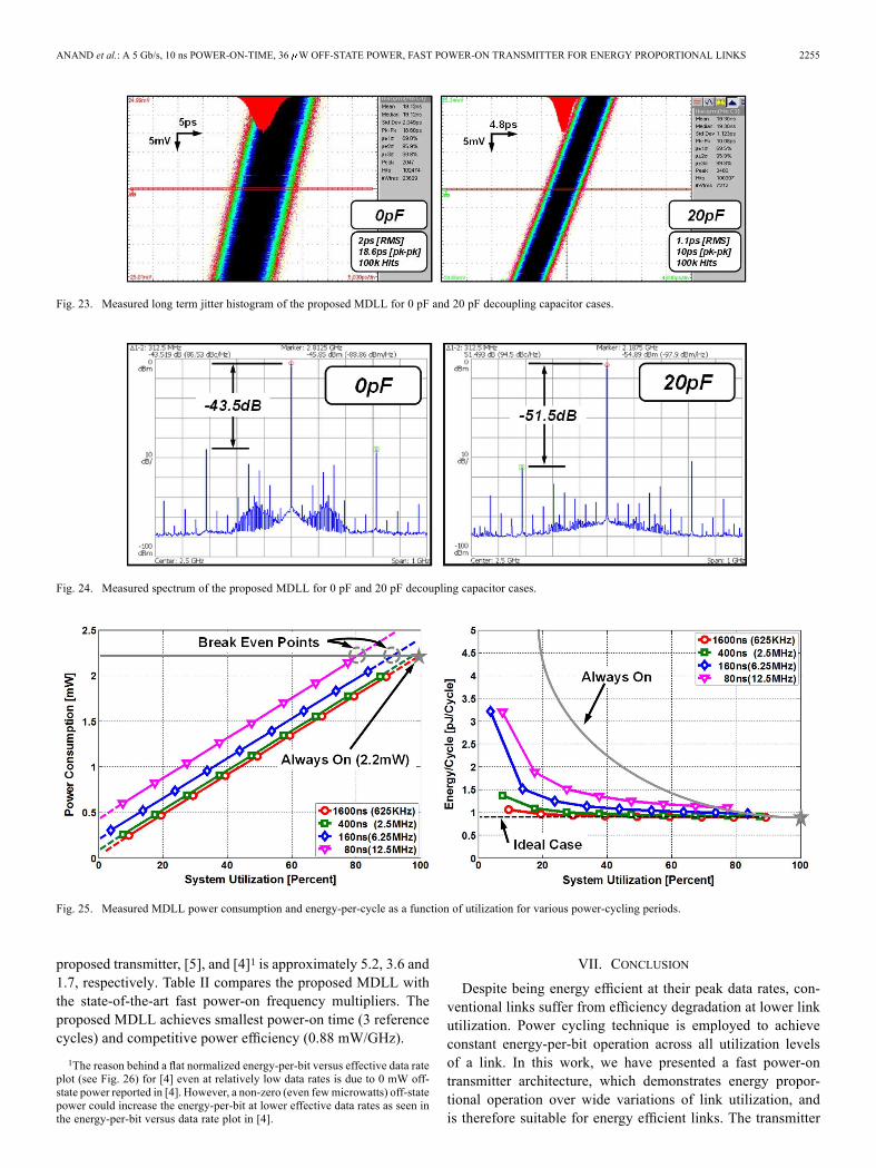
Fig. 23 shows the measured MDLL jitter performancefor two extreme capacitor values. The measured long termabsolute jitter over 100 k hits for a 20 pF decoupling ca-pacitor is 1.1 ps /10 ps , and for a 0 pF capacitoris 2 ps /18.6 ps . A big decoupling capacitor filtersthe noise from current sources and supply thereby achievingsuperior performance. A big decoupling capacitor also helps inreducing reference spurs. Fig. 24 shows the measured MDLL’soutput spectrum for two capacitor values.The measured reference spur for a decoupling capacitor of
20 pF and 0 pF is 51.5 dB and 43.5 dB, respectively. Webelieve common ground pins between the ripple counter, digitallogic, and VCO is the main reason for this spur and the spursappearing at subharmonic reference frequencies.Energy proportional performance of the stand alone MDLL
is measured separately. Fig. 25 shows the measured powerconsumption and energy-per-cycle versus utilization when theMDLL is power cycled at four different on/off periods. Thepower scales linearly with utilization. The average energy over-head of on-to-off and off-to-on transition is 12 pJ. A non-zeroy-intercept indicates finite turn-on time and non-zero off-statepower. In a conventional multiplier the energy-per-cycle in-creases at lower utilization. The proposed MDLL achieves
TABLE IPERFORMANCE COMPARISON OF THE PROPOSED FAST-ON TRANSMITTER
WITH STATE-OF-THE-ART DESIGNS
0.4 mW for 8 channels reportedOutput driver and clock power at 5 Gb/sOutput driver, clock and receiver power at 5.6 Gb/sOutput driver, clock and receiver power at 4.3 Gb/s
almost constant energy-per-cycle when power cycled witha cycle time of 1600 ns. For this case, the energy-per-cyclechanges from 0.88 pJ to 1 pJ when the utilization changes from100% to 9%. When MDLL is power cycled with a cycle timeof 400 ns, the energy-per-cycle changes from 0.88 pJ to 1.4 pJwhen the utilization changes from 100% to 7.5%.Table I compares the proposed transmitter with state-of-
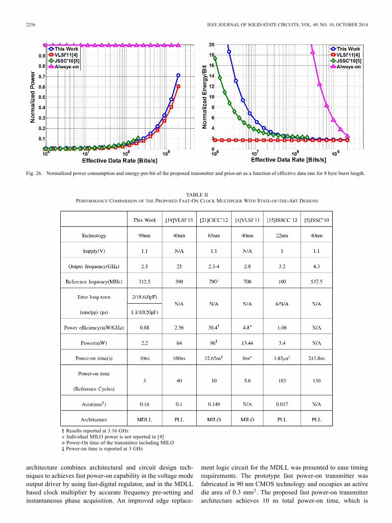
the-art designs. The proposed voltage mode driver comparesfavorably and achieves smallest power-on time. The trans-mitter as a whole achieves smallest power-on time in termsof reference cycles. Comparison of the proposed transmitterwith prior-art is made using normalized energy-per-bit versuseffective data rate and normalized power versus effective datarate plots. Burst length of 8 bytes is used in this compar-ison. Comparison plots were obtained based on the power-ontime, off-state power, and on-state power of the prior-art andproposed transmitter. Normalization of energy-per-bit versuseffective data rate was done such that, proposed transmitter andprior-art have unity energy efficiency at their respective peakdata rates. Normalization of power versus effective data ratewas done such that, proposed transmitter and prior-art haveunity power at their respective peak data rates. Fig. 26 showsthe comparison plot of normalized power versus effectivedata rate and energy-per-bit versus effective data rate. At aneffective data rate of 10 Mb/s, normalized energy-per-bit of the
ANAND et al.: A 5 Gb/s, 10 ns POWER-ON-TIME, 36 W OFF-STATE POWER, FAST POWER-ON TRANSMITTER FOR ENERGY PROPORTIONAL LINKS 2255
Fig. 23. Measured long term jitter histogram of the proposed MDLL for 0 pF and 20 pF decoupling capacitor cases.
Fig. 24. Measured spectrum of the proposed MDLL for 0 pF and 20 pF decoupling capacitor cases.
Fig. 25. Measured MDLL power consumption and energy-per-cycle as a function of utilization for various power-cycling periods.
proposed transmitter, [5], and [4]1 is approximately 5.2, 3.6 and1.7, respectively. Table II compares the proposed MDLL withthe state-of-the-art fast power-on frequency multipliers. Theproposed MDLL achieves smallest power-on time (3 referencecycles) and competitive power efficiency (0.88 mW/GHz).
1The reason behind a flat normalized energy-per-bit versus effective data rateplot (see Fig. 26) for [4] even at relatively low data rates is due to 0 mW off-state power reported in [4]. However, a non-zero (even fewmicrowatts) off-statepower could increase the energy-per-bit at lower effective data rates as seen inthe energy-per-bit versus data rate plot in [4].
VII. CONCLUSION
Despite being energy efficient at their peak data rates, con-ventional links suffer from efficiency degradation at lower linkutilization. Power cycling technique is employed to achieveconstant energy-per-bit operation across all utilization levelsof a link. In this work, we have presented a fast power-ontransmitter architecture, which demonstrates energy propor-tional operation over wide variations of link utilization, andis therefore suitable for energy efficient links. The transmitter
2256 IEEE JOURNAL OF SOLID-STATE CIRCUITS, VOL. 49, NO. 10, OCTOBER 2014
Fig. 26. Normalized power consumption and energy-per-bit of the proposed transmitter and prior-art as a function of effective data rate for 8 byte burst length.
TABLE IIPERFORMANCE COMPARISON OF THE PROPOSED FAST-ON CLOCK MULTIPLIER WITH STATE-OF-THE-ART DESIGNS
Results reported at 3.16 GHzIndividual MILO power is not reported in [4]Power-On time of the transmitter including MILOPower-on time is reported at 3 GHz
architecture combines architectural and circuit design tech-niques to achieves fast power-on capability in the voltage modeoutput driver by using fast-digital regulator, and in the MDLLbased clock multiplier by accurate frequency pre-setting andinstantaneous phase acquisition. An improved edge replace-
ment logic circuit for the MDLL was presented to ease timingrequirements. The prototype fast power-on transmitter wasfabricated in 90 nm CMOS technology and occupies an activedie area of 0.3 mm . The proposed fast power-on transmitterarchitecture achieves 10 ns total power-on time, which is

ANAND et al.: A 5 Gb/s, 10 ns POWER-ON-TIME, 36 W OFF-STATE POWER, FAST POWER-ON TRANSMITTER FOR ENERGY PROPORTIONAL LINKS 2257
limited by the clock multiplier, and consumes 4.8 mW/36 Won/off-state power from 1.1 V supply. The voltage mode driverand the clock multiplier achieve power-on-time of only 2 ns and10 ns, respectively. The transmitter achieves 100 effectivedata rate scaling (5 Gb/s–0.048 Gb/s), while scaling the powerand energy efficiency by only 50 (4.8 mW–0.095 mW) and2 (1–2 pJ/Bit), respectively.
ACKNOWLEDGMENT
The authors thank Berkeley Design Automation for providingthe Analog Fast Spice (AFS) simulator and the anonymous re-viewers for their helpful feedback.
REFERENCES
[1] F. O’Mahony, G. Balamurugan, J. Jaussi, J. Kennedy, M. Mansuri,S. Shekhar, and B. Casper, “The future of electrical I/O for micro-processors,” in Proc. IEEE Symp. VLSI Design Automation and Test(VLSI-DAT), 2009, pp. 31–34.
[2] G. Balamurugan, J. Kennedy, G. Banerjee, J. Jaussi, M. Mansuri, F.O’Mahony, B. Casper, and R. Mooney, “A scalable 5–15 Gbps, 14–75mW low-power I/O transceiver in 65 nm CMOS,” IEEE J. Solid-StateCircuits, vol. 43, no. 4, pp. 1010–1019, Apr. 2008.
[3] M. Mansuri, J. Jaussi, J. Kennedy, T. Hsueh, S. Shekhar, G. Bala-murugan, F. O’Mahony, C. Roberts, R. Mooney, and B. Casper, “Ascalable 0.128-to-1 Tb/s 0.8-to-2.6 pJ/b 64-lane parallel I/O in 32 nmCMOS,” in IEEE ISSCC Dig. Tech. Papers, 2013, pp. 402–403.
[4] J. Zerbe, B. Daly, W. Dettloff, T. Stone, W. Stonecypher, P.Venkatesan, K. Prabhu, B. Su, J. Ren, B. Tsang, B. Leibowitz, D.Dunwell, A. Carusone, and J. Eble, “A 5.6 Gb/s 2.4 mW/Gb/s bidirec-tional link with 8 ns power-on,” in Proc. IEEE Symp. VLSI Circuits,2011, pp. 82–83.
[5] B. Leibowitz, R. Palmer, J. Poulton, Y. Frans, S. Li, J. Wilson, M.Bucher, A. Fuller, J. Eyles, M. Aleksic, T. Greer, and N. Nguyen,“A 4.3 GB/s mobile memory interface with power-efficient bandwidthscaling,” IEEE J. Solid-State Circuits, vol. 45, no. 4, pp. 889–898, Apr.2010.
[6] F. O’Mahony, J. Jaussi, J. Kennedy, G. Balamurugan, M. Mansuri, C.Roberts, S. Shekhar, R. Mooney, and B. Casper, “A 47 10 Gb/s 1.4mW/Gb/s parallel interface in 45 nm CMOS,” , vol. 45, no. 12, pp.2828–2837, Dec. 2010.
[7] Energy Efficient Ethernet Task Force, 2010, IEEE P802.3az [Online].Available: http://grouper.ieee.org/groups/802/3/az
[8] K. Christensen, P. Reviriego, B. Nordman, M. Bennett, M. Mostowfi,and J. Maestro, “IEEE 802.3az: The road to energy efficient ethernet,”IEEE Commun. Mag., vol. 48, no. 11, pp. 50–56, Nov. 2010.
[9] L. Barroso and U. Holzle, “The case for energy-proportional com-puting,” Computer, vol. 40, no. 12, pp. 33–37, Dec. 2007.
[10] T. Anand, M. Talegaonkar, A. Elshazly, B. Young, and P. Hanumolu,“A 2.5 GHz 2.2 mW/25 W on/off-state power 2 ps -long-term-jitter digital clock multiplier with 3-reference-cycles power-on time,”in IEEE ISSCC Dig. Tech. Papers, 2013, pp. 256–257.
[11] H. Hatamkhani, K.-L. J. Wong, R. Drost, and C.-K. K. Yang, “A10-mW 3.6-Gbps I/O transmitter,” in Proc. IEEE Symp. VLSI Circuits,2003, pp. 97–98.
[12] Y. Okuma, K. Ishida, Y. Ryu, X. Zhang, P.-H. Chen, K. Watanabe,M. Takamiya, and T. Sakurai, “0.5-V input digital LDO with 98.7%current efficiency and 2.7- A quiescent current in 65 nm CMOS,” inProc. IEEE Custom Integr. Circuits Conf. (CICC), 2010, pp. 1–4.
[13] M. Onouchi, K. Otsuga, Y. Igarashi, T. Ikeya, S. Morita, K. Ishibashi,and K. Yanagisawa, “A 1.39-V input fast-transient-response digitalLDO composed of low-voltage MOS transistors in 40-nm CMOSprocess,” in Proc. IEEE Asian Solid-State Circuits Conf., 2011, pp.37–40.
[14] P. Hanumolu, M. Brownlee, K. Mayaram, and U.-K. Moon, “Analysisof charge-pump phase-locked loops,” IEEE Trans. Circuits Syst. I, vol.51, no. 9, pp. 1665–1674, Sep. 2004.
[15] N. August, H. Jin Lee, M. Vandepas, and R. Parker, “A TDC-lessADPLL with 200-to-3200 MHz range and 3 mW power dissipationfor mobile SoC clocking in 22 nm CMOS,” in IEEE ISSCC Dig. Tech.Papers, 2012, pp. 246–248.
[16] W.-H. Chiu, Y.-H. Huang, and T.-H. Lin, “A dynamic phase errorcompensation technique for fast-locking phase-locked loops,” IEEE J.Solid-State Circuits, vol. 45, no. 6, pp. 1137–1149, Jun. 2010.
[17] T.-H. Chien, C.-S. Lin, Y. Z. Juang, C.-M. Huang, and C.-L. Wey, “Anedge-missing compensator for fast-settling wide-locking-range PLLs,”in IEEE ISSCC Dig. Tech. Papers, 2009, pp. 394–395, 395a.
[18] K. Woo, Y. Liu, E. Nam, and D. Ham, “Fast-lock hybrid PLL com-bining fractional-N and integer-N modes of differing bandwidths,”IEEE J. Solid-State Circuits, vol. 43, no. 2, pp. 379–389, Feb. 2008.
[19] R. Navid, M. Hekmat, F. Aryanfar, J. Wei, and V. Gadde, “A 25 GHz100 ns lock time digital LC PLLwith an 8-phase output clock,” inProc.IEEE Symp. VLSI Circuits, 2013, pp. 196–197.
[20] M. Izad and C.-H. Heng, “A pulse shaping technique for spur suppres-sion in injection-locked synthesizers,” IEEE J. Solid-State Circuits,vol. 47, no. 3, pp. 652–664, Mar. 2012.
[21] D. Dunwell, A. Carusone, J. Zerbe, B. Leibowitz, B. Daly, and J. Eble,“A 2.3–4 GHz injection-locked clock multiplier with 55.7% lock rangeand 10-ns power-on,” in Proc. IEEE Custom Integr. Circuits Conf.(CICC), 2012, pp. 1–4.
[22] R. Farjad-rad,W.Dally, H.-T. Ng, R. Senthinathan,M.-J. Lee, R. Rathi,and J. Poulton, “A low-power multiplying DLL for low-jitter multigi-gahertz clock generation in highly integrated digital chips,” IEEE J.Solid-State Circuits, vol. 37, no. 12, pp. 1804–1812, Dec. 2002.
[23] S. Ye, L. Jansson, and I. Galton, “A multiple-crystal interface PLL withVCO realignment to reduce phase noise,” IEEE J. Solid-State Circuits,vol. 37, no. 12, pp. 1795–1803, Dec. 2002.
[24] G.-Y. Wei, J. Stonick, D. Weinlader, J. Sonntag, and S. Searles, “A 500MHz MP/DLL clock generator for a 5 Gb/s backplane transceiver in0.25 m CMOS,” in IEEE ISSCC Dig. Tech. Papers, 2003, vol. 1, pp.464–465.
[25] A. Elshazly, R. Inti, B. Young, and P. Hanumolu, “Clock multiplica-tion techniques using digital multiplying delay-locked loops,” IEEE J.Solid-State Circuits, vol. 48, no. 6, pp. 1416–1428, Jun. 2013.
[26] B. Helal, M. Straayer, G.-Y. Wei, and M. Perrott, “A highly digitalMDLL-based clock multiplier that leverages a self-scrambling time-to-digital converter to achieve subpicosecond jitter performance,” IEEEJ. Solid-State Circuits, vol. 43, no. 4, pp. 855–863, Apr. 2008.
[27] J. Poulton, R. Palmer, A. Fuller, T. Greer, J. Eyles, W. Dally, and M.Horowitz, “A 14-mW 6.25-Gb/s transceiver in 90-nm CMOS,” IEEEJ. Solid-State Circuits, vol. 42, no. 12, pp. 2745–2757, Dec. 2007.
[28] Y. Lu, W.-H. Ki, and C. Yue, “A 0.65 ns-response-time 3.01 psFOM fully-integrated low-dropout regulator with full-spectrumpower-supply-rejection for wideband communication systems,” inIEEE ISSCC Dig. Tech. Papers, 2014, pp. 306–307.
[29] J. Bulzacchelli, Z. Toprak-Deniz, T. Rasmus, J. Iadanza, W. Bucossi,S. Kim, R. Blanco, C. Cox, M. Chhabra, C. LeBlanc, C. Trudeau, andD. Friedman, “Dual-loop system of distributed microregulators withhigh dc accuracy, load response time below 500 ps, and 85-mV dropoutvoltage,” IEEE J. Solid-State Circuits, vol. 47, no. 4, pp. 863–874,2012.
[30] P. Hazucha, T. Karnik, B. Bloechel, C. Parsons, D. Finan, and S.Borkar, “Area-efficient linear regulator with ultra-fast load regula-tion,” IEEE J. Solid-State Circuits, vol. 40, no. 4, pp. 933–940, 2005.
Tejasvi Anand (S’12) is currently pursuing the Ph.D.degree at the University of Illinois, Urbana-Cham-paign, IL, USA. He received theM.Tech. degree (firstclass with distinction) in electronics design and tech-nology from the Indian Institute of Science, Banga-lore, India, in 2008.From 2008 to 2010, he worked as an Analog De-
sign Engineer at Cosmic Circuits (now a part of Ca-dence), Bangalore, on the design of analog-to-dig-ital converters. From 2010 to 2011, he worked as aProject Associate at Indian Institute of Science, Ban-
galore, where he was involved in the design of neural recoding system and RFbuilding blocks. His research interests are in energy efficient high-speed wire-line communication systems, frequency synthesizers, data converters and en-ergy efficient sensors.Mr. Anand received the Analog Devices Outstanding Student Designer
Award in 2013.

2258 IEEE JOURNAL OF SOLID-STATE CIRCUITS, VOL. 49, NO. 10, OCTOBER 2014
Amr Elshazly (S’04–M’13) received the B.Sc.(Hons.) and M.Sc. degrees from Ain Shams Univer-sity, Cairo, Egypt, in 2003 and 2007, respectively,and the Ph.D. degree from Oregon State Univer-sity, Corvallis, OR, USA, in 2012, all in electricalengineering.He is currently a Design Engineer at Intel
Corporation, Hillsboro, OR, USA, developinghigh-performance high-speed I/O circuits and archi-tectures for next generation process technologies.From 2004 to 2006, he was a VLSI Circuit Design
Engineer at AIAT, Inc. working on the design of RF building blocks. From 2006to 2007, he was with Mentor Graphics Inc., Cairo, designing multi-standardclock and data recovery circuits. His research interests include high-speedserial-links, frequency synthesizers, digital phase-locked loops, multiplyingdelay-locked loops, clock and data recovery circuits, data converter techniques,and low-power mixed-signal circuits.Dr. Elshazly received the Analog Devices Outstanding Student Designer
Award in 2011, the Center for Design of Analog-Digital Integrated Circuits(CDADIC) Best Poster Award in 2012, and the Graduate Research Assistantof the year Award in 2012 from the College of Engineering at the Oregon StateUniversity. He serves as a reviewer for the IEEE JOURNAL OF SOLID-STATECIRCUITS, IEEE TRANSACTIONS ON CIRCUITS AND SYSTEMS I AND II, IEEETRANSACTIONS ON VERY LARGE SCALE INTEGRATION SYSTEMS, IEEE Interna-tional Symposium on Circuits and Systems, IEEE International Conference ofElectronic Circuits Systems, and IEEE Asian Solid-State Circuits Conference.
Mrunmay Talegaonkar received the B.Tech. degreein electrical engineering and the M.Tech. degree inmicroelectronics and VLSI Design from Indian Insti-tute of Technology Madras, Chennai, India, in 2007.He is currently pursuing the Ph.D. degree at Univer-sity of Illinois, Urbana-Champaign, IL, USA.Between 2007 and 2009, he worked as a design
engineer at Analog Devices, Bangalore, India,where he was involved in design of digital-to-analogconverters. During 2009–2010, he was a projectassociate at Indian Institute of Technology Madras,
working on high speed clock and data recovery circuits. From 2010 to 2013,he was a research assistant, working on high speed links, at Oregon StateUniversity, Corvallis, OR, USA. His research interests include high speed I/Ointerfaces and clocking circuits.
Brian Young received the B.S. degree in electricalengineering from the Pennsylvania State Universityin 2000 and the Ph.D. degree from Oregon State Uni-versity in 2013.From 2000 to 2003, he was with the Timing
Solutions Operation of Motorola Semiconductor inChandler, AZ. From 2003 to 2007, he was with AMISemiconductor in Lower Gwynedd, PA. Since 2013,he has been with Marvell Semiconductor, Corvallis,OR. His research interests include time-based dataconverters, digital PLLs, and high performance
mixed-signal circuits.Dr. Young has received the 2010 and 2013 Analog Devices Outstanding Stu-
dent Designer Award.
Pavan Kumar Hanumolu (S’99–M’07) is cur-rently an Associate Professor in the Departmentof Electrical and Computer Engineering and aResearch Associate Professor with the CoordinatedScience Laboratory at the University of Illinois,Urbana-Champaign, IL, USA. He received the Ph.D.degree from the School of Electrical Engineeringand Computer Science at Oregon State University,Corvallis, in 2006, where he subsequently served asa faculty member till 2013. Dr. Hanumolu’s researchinterests are in energy-efficient integrated circuit
implementation of analog and digital signal processing, sensor interfaces,wireline communication system, and power conversion.Dr. Hanumolu received the National Science Foundation CAREER Award
in 2010. He currently serves as an Associate Editor of the IEEE JOURNAL OFSOLID-STATE CIRCUITS, and is a technical program committee member of theVLSI Circuits Symposium, and IEEE International Solid-State Circuits Confer-ence.


![2758 IEEE JOURNAL OF SOLID-STATE CIRCUITS, VOL. 49, NO. …circuits replace the OTAs in pipeline ADCs with power-effi-cient continuous-time slicers and current sources [5], [6], but](https://static.fdocuments.in/doc/165x107/5ed316299344585c674ebf13/2758-ieee-journal-of-solid-state-circuits-vol-49-no-circuits-replace-the-otas.jpg)