'IDW '99 ; 6 (Sendai) : 1999.12.01-03' - gbv.de · IDW'99 Proceedings of TheSixth International...
16
IDW '99 Proceedings of The Sixth International Display Workshops Workshops on • LC Science and Technologies • Active Matrix Displays • Passive Matrix LCDs • FPD Materials and Components •CRTs • Plasma Displays • EL Displays, LEDs, and Phosphors • Field Emission Display • Large-Area and Projection Displays, and Their Components • 3D Display Technologies and Human Factors December 1 -3, 1999 Sendai International Center Sendai, Japan UB/TIB Hannover 120 057 182 89 Sponsored by The Institute of Image Information and Television Engineers IT E | Kikai-Shinko-Kaikan, 3-5-8 Shiba-Koen, Minato-ku, Tokyo 105-0011, Japan The Society for Information Display, Japan Chapter M. Maeda, SID Japan Chapter Chair, c/o Display Device, Home Network Company, SONY, 4-16, Okata, Atsugi 243-0021, Japan SID JAPAN CHAPTER
Transcript of 'IDW '99 ; 6 (Sendai) : 1999.12.01-03' - gbv.de · IDW'99 Proceedings of TheSixth International...

IDW '99Proceedings
of
The Sixth International Display Workshops
Workshops on
• LC Science and Technologies• Active Matrix Displays• Passive Matrix LCDs
• FPD Materials and Components•CRTs
• Plasma Displays• EL Displays, LEDs, and Phosphors• Field Emission Display• Large-Area and Projection Displays,
and Their Components• 3D Display Technologies and
Human Factors
December 1 -3, 1999
Sendai International Center
Sendai, JapanUB/TIB Hannover120 057 182
89
Sponsored byThe Institute of Image Information and Television Engineers
ITE | Kikai-Shinko-Kaikan, 3-5-8 Shiba-Koen, Minato-ku, Tokyo 105-0011, Japan
The Society for Information Display, Japan Chapter
M. Maeda, SID Japan Chapter Chair, c/o Display Device,
Home Network Company, SONY, 4-16, Okata, Atsugi 243-0021, Japan
SIDJAPAN CHAPTER
IDW '99
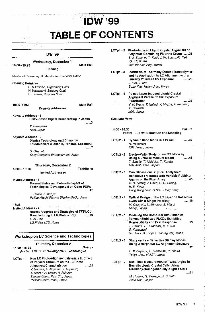
TABLE OF CONTENTS
IDW '99
10:00-10:15Wednesday, December 1
Main Hall
Opening
Master of Ceremony: H, Murakami, Executive Chair
Opening Remarks
S. Mikoshiba, Organizing Chair
H. Kawakami, Steering Chair
S. Tanaka, Program Chair
10:20-11:50 Main Hall
Keynote Addresses
Keynote Address -1
HDTV-Based Digital Broadcasting in Japan
T. Hasegawa
NHK, Japan
Keynote Address - 2
Display Technology and ComputerEntertainment (Console, Portable, Location)
S. Okamoto
Sony Computer Entertainment, Japan
Thursday, December 218:00-19:10 Tachibana
Invited Addresses
Invited Address -1
Present Status and Future Prospect of
Technological Development on Color PDPs
11
T. Hirose, K, KariyaFujitsu Hitachi Plasma Display (FHP), Japan
18:35
Invited Address - 2
Recent Progress and Strategies of TFT-LCD
Manufacturing in LG.Philips LCD 15
H.-S. Soh
LG.Philips LCD, Korea
Workshop on LC Science and Technologies
Thursday, December 2
14:00-16:30 Sakura
Poster LCTpl: Photo-Alignment Technologies
LCTpl -1 New LC Photo-Alignment Materials II: Effect
of Polymer Structure on the LC Photo-
Alignment Characteristics 21
Y. Nagase, E. Akiyama, Y. Miyama*,T. Nihira* H. Endo* H. Fukuro*
Sagami Chem. Res. Ctr., Japan*Nissan Chem. Inds., Japan
LCTpl - 2 Photo-Induced Liquid Crystal Alignment on
Polyimide Containing Fluorine Group 25
S.-J. Sung, H.-T. Kim*, J.-W. Lee, J.-K. Park
KAIST, Korea
Inst, for Adv. Eng., Korea
LCTpl - 3 Synthesis of Thermally Stable Photopolymerand Its Application to LC Alignment with a
Linearly Polarized UV Exposure 29
J. Kim, T. Kim
Sung Kyun Kwan Univ., Korea
LCTpl - 4 Pulsed Laser-Induced Liquid Crystal
Alignment Parallel to the ExposurePolarization 33
Y. H. Wang, T. Natsui, Y. Makita, A. Kumano,
Y. Takeuchi
JSR, Japan
See Late-News
14:00-16:30 Sakura
Poster LCTp2: Simulation and Modeling
LCTp2 -1 Dynamic Bend Mode in a Pi-Cell 37
H. Nakamura
IBMJapan, Japan
LCTp2 - 2 Electro-Optic Study of an IPS Mode by
Using a Uniaxial Medium Model 41
T. Satake, T. Nishioka, T. Kurata
Mitsubishi Elec, Japan
LCTp2 - 3 Two Dimensional Optical Analysis of
Reflective TN Modes with Variable Rubbing
Angles on the Pixel Array 45
D. D. Huang, J. Chen, H.-C. Huang,H. S. Kwok
Hong Kong Univ. ofS&T, Hong Kong
LCTp2 - 4 Optical Design of the LC Layer on Reflective
LCDs with a Single Polarizer 49
M. Okamoto, K. Minoura, S. Mitsui
Sharp, Japan
LCTp2 - 5 Modeling and ComputerSimulation of
Polymer Stabilized FLCDs ExhibitingMonostability and Fast Response 53
T. Umeda, T. Takahashi, H. Furue,
S. KobayashiSci. Univ. of Tokyo in Yamaguchi, Japan
LCTp2 - 6 Study on New Reflective Display Modes
Using Amorphous LC Alignment Structure
57
H. Kobayashi, Y. Takahashi, Y. iimura
Tokyo Univ. ofA&T, Japan
LCTp2 - 7 Real Time Measurement of Twist Angles in
Nematic Liquid Crystal Cells Using
Circularly-Homogeneously Aligned Cells
61
M. Honma, H. Yamaguchi, S. Sato
Akita Univ., Japan
IDW'99 V

TABLE OF CONTENTS
14:00-16:30
Poster LCTp3: New Panel Design
Sakura 10:40-12:10 Tachibana
LCTp3-1
LCTp3- 2
LCTp3- 3
LCTp3- 4
..65Method for Gap Formation in LCDs
V. A. Konovalov, A. A. Muravski,
S. N. Timofeev, S. Y. Yakovenko,S. T. Lagerwall*Inst. ofAppl. Phys. Problems, Belarus
*Chalmers Univ. of Tech., Sweden
Fabrication of Plastic Substrates with
Controlled Relief for Optical Componentsand Light Weight FPD 69
V. Belyaev, A. Volynski*, £ Voronina*
S. Bazhenov**, S. Ivanov*
AR Tech., Russia
*Moscow State Lomonosov Univ., Russia
**Semyonov Inst, of Chem. Phys., Russia
Negative Dielectric Anisotropic Liquid
Crystal Mixtures for TFT-LCD Applications
LCT2-1:
LCT2- 2
LCT2- 3
..73
S. T. Hong, W. C. Hu, J. L Lin, K. J. Chen,
S. T. WW
UCL, ITRI, Taiwan
*HRL Lab., USA
High Contrast PDLC Panels Having a Matrix
in which Pole Directions are RandomlyDistributed in a Plane 77
K. Nakao, H. Kubota, T. Uemura
Matsushita Elec. Ind., Japan
LCT2: Polymer-Based LCDs
Invited Holographically-Formed Polymer
Dispersed Liquid Crystal Reflective
Displays: A Diffusion Model Description..97
See Late-News
C. C. Bowley, G. P. Crawford
Brown Univ., USA
Transmission-Type Alignment-Controlled
Holographic PDLC for Reflective Displays101
M. Date, T. Hisaki
NTT, Japan
Drive-Voltage Reduction for HPDLC Displays105
J. K. Colegrove*'**, H. Yuan**, T. Fiske**,S.-T. Wu***, J. R. Kelly*, C. Bowley****,G. P. Crawford****
*Kent State Univ., USA
**dpiX, USA
***HRL Lab., USA
****Brown Univ., USA
LCT2-4: Invited Integral-Color Plastic LCD - The
Ultimate Flat Panel Display 109
C. Chiulli, J. DelPico, W. Vetterling,K. M. Johnson*, G. D. Sharp*, M. Schadt**,H. Seiberle**
Polaroid, USA
*ColorLink, USA
**ROLIC Res., Switzerland
Friday, December 3
9:00-10:25 Tachibana
LCT1: Photo-Alignment Technologies
LCT1 -1:
LCT1- 2
LCT1- 3
LCT1- 4
Invited Recent Progress in Optical
Alignment for LCDs 81
W. M. Gibbons, B. P. McGinnis, P. J. Shannon,
S. T. Sun, H. ZhengElsicon, USA
New LC Photo-Alignment Materials I:
Aromatic Polyamides with High Sensitivityand Stability 85
V. Miyama, T. Nihira, H. Endo, H. Fukuro,
E. Akiyama*, Y. Nagase*Nissan Chem. Inds., Japan
*Sagami Chem. Res. Ctr„ Japan
LC Alignment Properties of Photo-AlignmentMaterials Based on co-(4-chalconyloxy)alkylGroups 89
S. Nakata, K. Kuriyama, M. Kimura,
T. Natsui, Y. Makita, Y. Matsuki, A. Kumano,Y. Takeuchi
JSR, Japan
Fabrication of Defect Free FLCDs Using
Photo-Alignment and Their Characteristics
93
R. Kurihara, H. Fume, T. Takahashi,
S. Kobayashi
Sci. Univ. of Tokyo in Yamaguchi, Japan
14:00 -15:20 Tachibana
LCT3: Novel LC Technologies
LCT3 - 1 A Reflective HAN-LCD Compensated by a
DiscoticFilm 113
V. Tanaka, Y. limura
Tokyo Univ. ofA&T, Japan
LCT3 - 2 Reflective Three-Layer GH-LC Panel
Fabricated by Using Lithographic LC/Resist
Composite Films 117
N. Wakita, Y. Yamanaka
Matsushita Elec. Ind., Japan
LCT3 - 3 Homeotropic Alignment of Liquid Crystals
by Single Evaporation of Si02 121
M. Lu, K. H. Yang, J. S. CheyIBM, USA
LCT3 - 4 Liquid Crystal Switching Using Comb-on-
Plane Electrodes 125
Z. Meng, H. S. Kwok, M. Wong
Hong Kong Univ. ofS&T, Hong Kong
15:40 -17:00 Tachibana
LCT4: Polarization Effects in LC Devices
LCT4 -1 Wide-Viewing Display Configuration of
Helix-Deformed Ferroelectric Liquid Crystals129
J.-H. Lee, C.-J. Yu, D.-H. You, S.-D. Lee
Seoul Nat. Univ., Korea
VI IDW '99
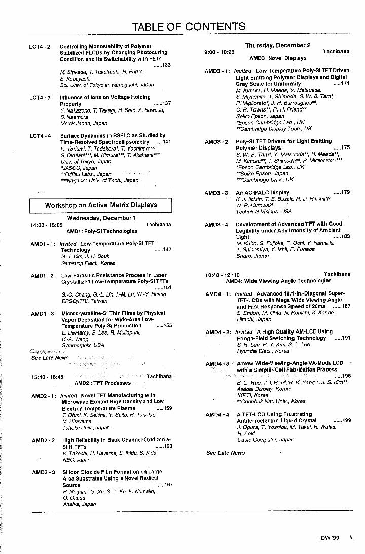
TABLE OF CONTENTS
LCT4 - 2 Controlling Monostability of Polymer
Stabilized FLCDs by Changing PhotocuringCondition and Its Switchability with FETs
133
M. Shikada, T. Takahashi, H. Fume,
S. KobayashiSci. Univ. of Tokyo in Yamaguchi, Japan
LCT4 - 3 Influence of Ions on Voltage Holding
Property 137
Y. Nakazono, T, Takagi, H. Sato, A. Sawada,
S. Naemura
Merck Japan, Japan
LCT4 - 4 Surface Dynamics in SSFLC as Studied by
Time-Resolved Spectroellipsometry 141
H. Toriumi, T. Tadokoro*, T. Yoshihara**,
S. Okutani***, M. Kimura***, T. Akahane***
Univ. of Tokyo, Japan
*JASCO, Japan
**Fujitsu Labs., Japan
***Nagaoka Univ. of Tech., Japan
Workshop on Active Matrix Displays
Wednesday, December 1
14:00-15:05 Tachibana
AMD1: Poly-Si Technologies
AMD1 -1: Invited Low-Temperature Poly-Si TFT
Technology 147
H. J. Kim, J. H. Souk
Samsung Elect., Korea
AMD1 - 2 Low Parasitic Resistance Process in Laser
Crystallized Low-Temperature Poly-Si TFTs
151
S.-C. Chang, G.-L. Un, l.-M. Lu, W.-Y. Huang
ERSO/ITRI, Taiwan
AMD1 - 3 Microcrystalline-Si Thin Films by Physical
Vapor Deposition for Wide-Area Low-
Temperature Poly-Si Production 155
E. Demaray, B. Lee, R. Mullapudi,K.-A. Wang
Symmorphix, USA
See Late-News
Thursday, December 2
9:00-10:25 Tachibana
AMD3: Novel Displays
AMD3 -1: Invited Low-Temperature Poly-Si TFTDriven
Light Emitting Polymer Displays and Digital
Gray Scale for Uniformity 171
M. Kimura, H. Maeda, Y. Matsueda,
S. Miyashita, T. Shimoda, S. W. B. Tarn*,
P. Migliorato*, J, H. Burroughes**,C. R. Towns**, R. H. Friend**
Seiko Epson, Japan
*Epson Cambridge Lab., UK
**Cambridge Display Tech., UK
AMD3 - 2 Poly-Si TFT Drivers for Light Emitting
Polymer Displays 175
S. W.-B. Tarn*, Y. Matsueda**, H. Maeda**,
M. Kimura**, T. Shimoda**, P. Migliorato*1***
*Epson Cambridge Lab., UK
**Seiko Epson, Japan
***Cambridge Univ., UK
AMD3 - 3 An AC-PALC Display 179
K. J. Ilcisin, T. S. Buzak, R. D. Hinchliffe,
W. R. Kurowski
Technical Visions, USA
AMD3 - 4 Development of Advanced TFT with Good
Legibility under Any Intensity of Ambient
Light 183
M. Kubo, S. Fujioka, T. Ochi, Y. Narutaki,T. Shinomiya, Y. Ishii, F. Funada
Sharp, Japan
10:40-12:10 Tachibana
AMD4: Wide Viewing Angle Technologies
AMD4-1: Invited Advanced 18.1-in.-Diagonal Super-TFT-LCDs with Mega Wide Viewing Angle
and Fast Response Speed of 20ms 187
S. Endoh, M. Ohta, N. Konishi, K. Kondo
Hitachi, Japan
AMD4-2: Invited A High Quality AM-LCD Using
Fringe-Field Switching Technology 191
S. H. Lee, H. Y. Kim, S. L. Lee
Hyundai Elect., Korea
AMD4 - 3
15:40-16:45 Tachibana
AMD2 : TFT Processes
AMD2-1: Invited Novel TFT Manufacturing with
Microwave Excited High Density and Low
Electron Temperature Plasma 159
T. Ohmi, K. Sekine, Y. Saito, H. Tanaka,
M. HirayamaTohoku Univ., Japan
AMD2 - 2 High Reliability in Back-Channel-Oxidized a-
Si:HTFTs 163
K. Takechi, H. Hayama, S. Ihida, S. Kido
NEC, Japan
AMD2 - 3 Silicon Dioxide Film Formation on LargeArea Substrates Using a Novel Radical
Source 167
H. Nogami, G. Xu, S. T. Ko, K. Numajiri,O. Okada
Anelva, Japan
A New Wide-Viewing-Angle VA-Mode LCD
with a Simpler Cell Fabrication Process
195
B. G. Rho, J. I. Han*, B. K. Yang**, J. S. Kim**
Asadal Display, Korea
*KETI, Korea
**ChonbukNat. Univ., Korea
AMD4 - 4 ATFT-LCD Using FrustratingAntiferroelectric Liquid CrystalJ. Ogura, T. Yoshida, M. Takei, H. Wakai,
H. Aoki
Casio Computer, Japan
,199
See Late-News
IDW '99 VII

TABLE OF CONTENTS
14:00-15:05 TachibanaAMDS: High Resolution/Reflective Technologies
AMD5-1: Invited Super High Resolution AM-LCD
Technology 203
R. L. Wisnieff
IBM, USA
AMD5 - 2 A 7.94ppm, 10-cm-Diagonal TFT-LCD UsingLow-Temperature Poly-Si Technology
207
M. Miyatake, T. Maeda, K. Nagayama,T. Morita, K. Kimura, K. Kawamata
Toshiba, Japan
AMD5 - 3 A Full-Color Reflective TFT-LCD Using an
Reflective Optically Compensated Twist
Mode with Wide Viewing Angle 211
M. Shibazaki, T. Ishinabe, T. Miyashita,T. Uchida, K. Yoshida*. H. Tanaka*, T. Sunata*
Tohoku Univ., Japan*Hosiden & Philips Display, Japan
AMDp - 4 New Bias Voltage Generators for TFT-LCD's
Drivers 239
M. Hirata, Y. Suzuki, M. Yoshida,
Y. Arayashiki, M. Teramoto, S. Choomchuay*Tokai Univ., Japan*ReCCIT/KMITL, Thailand
AMDp - 5 LCD Circuit Optimization by Genetic
AlgorithmS. Hatta
Matsushita Elec. Ind., Japan
See Late-News
..243
Workshop on Passive Matrix LCDs
15:40-16 :50 Tachibana
AMD6: Plastic Substrates
AMD6-1: Invited Passive-Matrix and MIM-Driven LCDs
with Plastic Substrates 215
E. Lueder
Univ. of Stuttgart, Germany
Thursday, December 2
14:00-15:20 Shirakashi 2
PLC1: Enhanced Passive Matrix LCDs
PLC1 -1: Invited Advanced Reflective Color
STN-LCDs 249
S. Komura, K. Kuwabara, O. Itou, M. Abe,K. Funahata, K. Kondo, N. Hoshino,Y. Iwakabe
Hitachi, Japan
PLC1 - 2: Invited Plastic LCD for Mobile Application.253
AMD6-2: Invited Low-Temperature Poly-Si for AM-LCDs on Glass and Polymer Substrates
..219
N. D. Young, I. D. French, M. J. Trainor,
D. T. Murley, D. J. McCulloch, R. W. Wilks
Philips Res. Labs., UK
AMD6 - 3 Characteristics of Low-Temperature-Processed a-Si TFT on Plastic Substrates
..223
M. Ikeda, Y. Mizutani, S. Ashida, K Yamada
Toshiba, Japan
Friday, December 3
14:00-16:30 Sakura
Poster AMDp: Active Matrix Displays
AMDp - 1 High Crystallinity Poly-Si by Excimer Laser
Annealing of Macrocrystalline Si 227
K. H. Jang, J. N. Lee, M. G. Lee, W. Y. So,K. N. Kim, H. D. Kim
Samsung Display Devices, Korea
AMDp - 2 Evaluation Method for Viewing Angle of TFT-
LCDs Based on Overall Picture Quality231
T. Suzuki, W. Song, J. Noguchi,Y. Shimodaira, G. Ohashi
Shizuoka Univ., Japan
AMDp - 3 Cost Effective Reticule Design for Very HighResolution Si Backplane Prototypes 235
J. Van den Steen, H. De Smet,G. Van Doorselaer, A. Van Calster, P. Colson*
Univ. of Gent, Belgium*Alcatel Microelect, Belgium
M. Watanabe, Y. Inoue, S. Fukuchi
Sharp, Japan
PLC1 - 3 Gray Scale Addressing Method byMulti-Order Paraunitary/OrthogonalBuilding Blocks 257
S. Yeung, J. Lee, B. Lam, J. Ng, I. Tsoi
Varitronix, Hong Kong
PLC1 - 4 Suitable Addressing Schemes for Mobile
Phone STN-LCDs 261
K. Tamai, M. Nagai, A. Nakazawa,
M. Kitamura, Y. Hirai, S. Matsuoka*, Y. Soda*
Asahi Glass, Japan*Optrex, Japan
15:40-17:00 Shirakashi 2
PLC2: New Modes and
Novel Addressing Technologies
PLC2 -1: Invited Recent Studies of Multiplex Drivingfor BTN-LCDs 265
H. Nomura, T. Obikawa, Y. Ozawa, T. Tanaka
Seiko Epson, Japan
PLC2 - 2: Invited The Parametric Analysis of a BTN-
LCD by using Computer Simulation 269
J.-S. Oh, S.-C. Pang, H.-Y. Lee, J.-G. Yoo,
K.-H. Kang, E.-S. Lee
Samsung Display Devices, Korea
PLC2 - 3 A New Codeword-Addressing Technique for
Low-Cost Driving of High-Resolution
Passive-Matrix Displays 273
A. P. Aitken
Hewlett-Packard Labs., UK
VIII IDW '99

TABLE OF CONTENTS
..277
PLC2 - 4 Electro-Optical Characteristics and
Optimizations of Vertically AlignedSTN-LCDs
V. Iwamoto
Stanley Elec, Japan
Friday, December 3
14:00-16:30 Sakura
Poster PLCp: Novel Studies in Passive Matrix LCDs
PLCp -1 Development of a New GH-Mode Reflective
LCD with High Dichroic Ratio 281
M. Kawaguri, Y. Yamanaka, N. Wakita
Matsushita Elec. Ind., Japan
PLCp-2
PLCp - 3
PLCp-4
PLCp-5
PLCp-6
A GH-LCD with Slightly Tilted
Homeotropically Aligned NLC Having a
Negative Dielectric Constant Prepared by
Photo-Alignment 285
H. Ushinohama, H. Yoshikawa, H. Fume,T. Takahashi, S. KobayashiSci. Univ. of Tokyo in Yamaguchi, Japan
Dependence of Light-Leakage Caused byDomain Formation Around Spacers on
Liquid Crystal Mixture in Normally Black
Mode LCDs 289
Y. Utsumi, S. Komura, Y. Iwakabe,
S. Matsuyama, K. Kondo
Hitachi, Japan
Key Technologies for the FLC Displays
Having Wide Operation Temperature 293
A. Sakaigawa, T. Sako, T, Furukawa,
M. Kabe, A. Tagawa, S. Okazaki, M. Koden
Sharp, Japan
Reflective Type Antiferroelectric LCD with a
Single Polarizer 297
D.-H. You, J.-H. Lee, J.-H. Park, S.-D. Lee
SeoulNat. Univ., Korea
FMC1 - 3 Characteristics of Rewritable Media UtilizingSmectic A PDLC Films 315
K. Sekine, W. Saito, A. Baba
Dai Nippon Printing, Japan
15:40-16:55 Shirakashi 1
FMC2: Projection Systems
FMC2 -1: Invited Overview of Head Mounted Display
Technology and Applications 319
H. Ong, M. Presz
Kopin, USA
FMC2-2: Invited Ultra High Contrast Screen 323
H. Sekiguchi, M. Honda, K. Oda
Dai Nippon Printing, Japan
FMC2 - 3: Invited Screens for Rear Projection LCD
..327
J. A. Shimizu, J. Goldenberg
Philips Res., USA
Design Optimization of BTN-LCD
S. Yeung, S. K Kwok, B. Fok, B. Lam,
C. Chang, I. Tsoi
Varitronix, Hong Kong
..301
See Late-News
Workshop on FPD Materials
and Components
Wednesday, December 1
14:00-15:10 Shirakashi 1
FMC1: Technology Trends of FPD
FMC1-1: Invited Display Manufacturing Alternatives
and Their Cost Effectiveness 307
S. Takata
Advanced Data Res., Japan
FMC1-2: Invited Optical Films for Increased
Readability in Reflective LCDs
W. Hibbard, T. Jones, S. C. Webster,
D. Wortman
3M, USA
..311
See Late-News
Thursday, December 2
9:00-10:30 Shirakashi 1
FMC3: Reflective LCDs
FMC3-1: Invited Recent Advances in Reflective LCDs
331
J. A. M. M. van Haaren, C. Doornkamp,
H. J. Cornelissen, L. J. M. Schlangen,J. P. A. Deeben, P. van de Witte,
R. van Asselt, A. V. Henzen
Philips, The Netherlands
FMC3 - 2: Invited Multi-Color Cholesteric Display
Using a Plastic Substrate 335
J. L. West, V. Bodnar, Y. Kim, H. WonderlyKent State Univ., USA
FMC3 - 3 Improved Reflectors for Ambient Lit Hand
Held Displays 339
ft Clabburn, A. M. Fairhurst, F. Konishi*
Microsharp, UK
innovation Partners Int., Japan
FMC3 - 4 Optical Characteristics of a Linear Polarizer
for Reflective LCDs 343
T. Uwano, H. Seki, T. Uchida*
Hachinohe Inst, of Tech., JapanTohoku Univ., Japan
10:40-12:05 Shirakashi 1
FMC4: LCD Backlighting and Others
FMC4 -1: Invited No-Mercury Flat Discharge Lamp for
LCD Backlighting 347
T. Shiga, S. Mikoshiba, S. Shinada*
Univ. of Electro-Commun., Japan
*Hitachi Lighting Equipment, Japan
FMC4 - 2 A Novel Cold Cathode Fluorescent Lamp
with an Adiabatic Layer 351
K. Nishimura, N. Tsutsui
Toshiba Lighting & Tech., Japan
IDW '99 IX

TABLE OF CONTENTS
..355
FMC4-3 A New Approach for Overlay and
Registration ImprovementL Leonardsson, P. Ekberg, K. EdgrenMicronic Laser Syss., Sweden
FMC4 - 4 Development of a Thermal CrosslinkingPhotoresist for LCD 359
T. Nishino, K. Niwa, M. Endo
JSR, Japan
See Late-News
14:00-15:25 Shirakashi 1
FMC5: Color Filters
FMC5 -1: Invited Development of a Color Filter for
LCDs Based on Polyimide Materials 363
Y. Sakurai
Toray Ind., Japan
FMC5 - 2 Development of a New Color Set of Transfer-
Type Color Filter Materials for LCDs 367
H. Yoshino, K. Hasebe, H. Ito
Fuji Photo Film, Japan
FMC5 - 3 Resin Black Matrix for Color Filters 371
M. Yoshioka, K. Inoue, J. Tsukamoto, T. Goto,K. Shimizu
Toray Ind., Japan
FMC5 - 4 Chemically Amplified Resin Black Matrix
System 375
S. Dan, N. Suzuki
Fujifilm Olin, Japan
See Late-News
15:40 -17:05 Shirakashi 1
FMC6: Optical Films
FMC6 - 1 Bright Reflective Color Filters Based on
Cholesteric Liquid Crystral Materials 379
D, Reddy, A. Hochbaum, Y. JiangCLC Display, USA
FMC6-2: Invited Advancement in Wide-Viewing-Angle
LCDs 383
l.-W. Wu, D.-L. Ting, C.-C. ChangERSO/ITRI, Taiwan
FMC6 - 3 Homeotropically Aligned Thin Layer of
Discotic Liquid Crystals by Coating Method
387
K. Kawata, H. Nishikawa, S. Yokoyama,M. Ichihashi, M. Okazaki
Fuji Photo Film, Japan
FMC6 - 4 Design of AG Treatment on Display Surface
for High Resolution LCDs 391
S. Kobayashi, H. Shibata, Y. Takahashi,
T. Shouda
Nitto Denko, Japan
14:00-16:30 Sakura
Poster FMCp: FPD Materials and Components
FMCp -1 Low-Refractive-Index Materials for Wet
Process Coating System 395
N. Oikawa, N. Kunimine, Y. Ohta, T. Yoshihara
Dai Nippon Printing, Japan
FMCp - 2 Visibility Evaluation of AG Films for LCDs
and Design of a Novel AG Film 399
G. Furui, T. Matsuoka, Y. Iwata, N. Nakamura,S. Umise
Dai Nippon Printing, Japan
FMCp - 3 Diffusive Layer for Reflective Type LCDs
403
M. Miyatake, S. Yano, T. Sakuramoto, K Hara,K. Kawamura, Y. Fujimura,Nitto Denko, Japan
FMCp - 4 Hybrid Aligned Rod-like Liquid CrystallinePolymer Film as Viewing Angle
Compensator for NW-TN-LCDs:
Improvement of Gray Scale Performance
407
T. Kaminade, E. Yoda, K. Suzuki,T. Toyooka, Y. Kobori, K. Inoue*, T. Kurita*
Nippon Mitsubishi Oil, Japan*Nippon Petrochems., Japan
FMCp - 5 Optical Anisotropy of PhenylacetyleneHomologs : The Effects of Core Substituent
Groups 411
C. Sekine, K. Fujisawa, N. Kenya, M. Minai''Sumitomo Chem., Japan
FMCp - 6 A New Photoresist for LCD Panel Spacer415
T. Okita, Y. Masaki
Fujifilm Olin, Japan
FMCp - 7 Novel Topcoat Planarization Derived from
CardoEpoxy 419
K. Sasaki, S. Kazama, Y. Miyagawa,Y. Uchimiya, K. Fujishiro
Nippon Steel Chem., Japan
FMCp - 8 Luminosity Compensation Method at Low
Temperatures by a Heater for Automobile-
Use Back Light 423
K. Matsunaga, Y. Wagatsuma*Toshiba AVE, Japan'Toshiba Lighting & Tech., Japan
FMCp - 9 2.2$ Double Tube Cold Cathode Fluorescent
Lamp 427
T. Nishihara, Y. Tomita
Harison Elec, Japan
FMCp -10 Novel Color Switching Mode in Fluorescent
LCDs 431
ft Yamaguchi, J. Kishida, S. Sato
Akita Univ., Japan
FMCp -11 An Inspection System and Methods for Pixel
Defects in LCDs 435
F. Saitoh
Iwate Pref. Univ., Japan
Workshop on CRTs
Wednesday, December 1
13:45-15:25
CRT1: CRTs and CRT AppliancesHagi
CRT1 -1: Invited Recent CRT Display Monitors and
Some Proposals to CRT for Survival 441
H. Kofune
LG Elect, Korea
X IDW '99

TABLE OF CONTENTS
CRT1-2: Invited A Design Concept of Perfect-Flat
CRT 445
T. Saito
Sony, Japan
CRT1 - 3 A New 46-cm DIAMONDTRON NF CRTfor
Display Monitors 449
T. Hirano, T. Otawa, T. Karita, K. Nagasawa,N. Hinomoto, M. NoguchiMitsubishi Elec, Japan
CRT1 - 4 46-cm 100° Super-High Deflection SensitivityColor Display Tube 453
K. Soneda, Y. Fukuda, M. Ishikawa, J. Kimiya,
S. SugawaraToshiba, Japan
CRT1 - 5 A 61-in. HD Projection TV with a Two-Mode
Digital Convergence System 457
K. Yoshizawa, T. Watanabe, S. Hatakeyama,
T. Nakiri, M. Tsukahara*. K, Matsumi*
Hitachi, Japan*Hitachi Video & Info., Japan
15:40-17:00
CRT2: Topical Session for Simulation Technologies
CRT2-1: Invited ProGUN: 3-D Electron Gun
Simulator 461
H. Y. Ahn, J. N. Kim, H. W. Jang, M. Fukushima
Samsung Display Devices, Korea
CRT2 - 2: Invited Simulation System of Deflection
Yoke for CRTs 465
H. Miyazawa, K. Oku, T. Hisada, N. /to*
H. Fukumoto, M. Koizumi, S. Shiral
Hitachi, Japan'Hitachi Media Elect, Japan
CRT3 - 4 Comparison Between Rectangular and
Circular Magnetic Cores of CRT Deflection
Yokes 489
K. Uchibori, T. Tsuchiya, H. Inoue
Totoku Elec, Japan
10:35-12:15 HagiCRT4: Glass and Surface Coating
CRT4-1: Invited Development of Low TemperatureFrit Glass for CRTs 493
M. Hayashi, Y. Jimura, K. Shindo, M. Kyono,N. Daiku, ft Schmidtz*. J. Bobinski*
Nippon Elect. Glass, Japan
*Technoglas, USA
CRT4 - 2 Anti-Contamination Coating for CRT Glass
497
M. Sasaki, S. Rokudai, S. Takeda
Asahi Glass, Japan
CRT4 - 3 Transmission Controlled Panel Glass for
CRT: "G-WARAS" 501
N. Horie, T. Sugawara, T. OyamaAsahi Glass, Japan
CRT4 - 4 The Temperature Variation Between Bulbs
Due to the Change of Inner Diameter of
Baffle Plate in Main Sealing Furnace 505
/. Cho, W. Soh, G. Lee
Samsung Display Devices, Korea
CRT4 - 5 A New Antistatic Coating Layer for CRT
Faceplate Using the Organic Conductive
Polymer 509
C.-H. Lee, H.-S. Sohn
Orion Elec, Korea
..469CRT2 - 3: Invited CRT Glass Modeling
J. J. GaviganSarnoff, USA
CRT2 - 4 Calculation of Phosphor Grain Size Effects
on CRT Screen Performance 473
H. Glaser, H. Bechtel, F. Busse, J. Kikkert*
Philips Res. Labs., Germany
*Philips Comps., TheNetherlands
Thursday, December 29:00-10:20 Hagi
CRT3: DY and Mask
CRT3 -1: Invited An Improved Mask Corner
Suspension for Real Flat Wide Screen Color
Picture Tubes 477
A. A. M. Hendriks
Philips Comps., The Netherlands
CRT3 - 2 Effect of Damping Wire on Aperture Grille
Vibration 481
V. Ohmura, M. Hashimoto, H. Taguchi
Sony, Japan
CRT3 - 3: Invited Simulation of Magnetic Shielding for
CRTs 485
A. Haga, H. Nasuno*, H. Ikeda**
Tohoku Gakuin Univ., Japan
*Polytechnocenter Miyagi, Japan
**Mitsubishi Elec, Japan
4:00-15:40 Hagi
CRT5: Electron Guns
CRT5 -1 Stabilization of CRT Performance by
Optimizing Gun Beading Condition 513
S. H. Lee
Orion Elec, Korea
CRT5 - 2 Development of a NEXT Electron Gun for
46-cm 100° Narrow Neck Color Display
Tubes 517
T. Nakamura, K. Noguchi, Y. Yatsu, S. Shirai
Hitachi, Japan
CRT5 - 3 A New Electron Gun for Color Monitor Tubes
with Large and Perfectly Flat Screen 521
y. Wada, T. Daimon
Matsushita Elect, Japan
CRT5 - 4 A Newly Developed Electron Gun for 19-in.
CDTs 525
H. C. Kim, K. B. Son, S. H. Cho, T. K. Kim,
D. Y. Kim, W. H. Kim
LG Elect, Korea
CRT5 - 5 Technology for a Very Small Aperture G1
with l-Cathodes 529
M. Mizuki, H. Tobita, Y. Amano
Sony, Japan
IDW '99 XI
TABLE OF CONTENTS
16:00-17:00 HagiCRT6: Cathodes
CRT6 -1 A Newly Developed HIP Cathode Sintered
under High Temperature and High Pressure533
T. Sugimura, M. Narita, ft Takeda, T. Hirai
NECKansai, Japan
CRT6 - 2 A Study on the Emission Characteristics of a
SC2O3-Dispersed Oxide Cathode 537
K.-C. Chou, H.-C. Cheng, C.-C. Chen,
C.-H. Yeh
Chunghwa Picture Tubes, Taiwan
CRT6-3 Area-Restricted Cathode for CRTs 541
T. Shiroishi, T. Ohira, H. Teramoto,S. Nakata, K. Oono
Mitsubishi Elec, Japan
See Late-News
Friday, December 3
14:00-16:30 Sakura
Poster CRTp: CRTs
CRTp -1 AYAG Rear Projection Display for
Multimedia Application 545
J. Cheng, Z. Chen, G. Huang, Z. Lin, G. Cao
Univ. of Elect. S&Tof China, China
CRTp - 2 A Self-Circulating Cooling System Used in a
3-in. YAG Projection CRT 549
0. Ran, J. Wang, G. Li, Z. Li, Z. Lin, J. ChengUniv. of Elect. S&T of China, China
CRTp - 3 Assembling Method of a CRT with an Inner
Yoke 553
X. Li, Y. Zheng, L. U
Southeast Univ., China
CRTp - 4 A GUI Program for Convergence Simulation
of CRT 557
J. S. Fang, C. L. LiangTECO Info. Sys„ Taiwan
CRTp - 5 Simulation of Electron Guns Including
Space Charge 561
ft Harthoorn, D. Roozendaal
Philips Display Comps., The Netherlands
CRTp-6 New Photo Cathode Display 565
y. Sakamoto, H. Tanaka, A. Kuroda*,K. Takekawa**
Kanazawa Inst, of Tech., Japan
*NEC, Japan**Matsushita Elect., Japan
CRTp - 7 Center-Vibration of a Trinitron Aperture Grill
569
T. Aoki, KSaita
Sony, Japan
CRTp - 8 Stretched Tension Mask with Large Vertical
Pitch for CPTs 573
S. W. Ko, J.-E. Choi, P.-S. Jung,N.-J. Koh
LG Elect, Korea
CRTp - 9 Newly Developed Simulation Modeling of an
IMS 577
S. Nakata, K. Nishimura, S. Okuda
Mitsubishi Elec, Japan
CRTp -10 A Reactive Sputter-Coating on CRT's
Surface
Y.-M. Teng, H.-S. Tong, C.-M. Hu
Chunghwa Picture Tubes, Taiwan
..581
Workshop on Plasma Displays
9:00-10:20Thursday, December 2
PDP1: Panel Configurations
Main Hall
PDP1 -1: Invited High Luminance AC-PDPs with
Waffle-Structured Barrier Ribs 587
T. Komaki, H. Taniguchi, K. Amemiya
Pioneer, Japan
PDP1 - 2 Improvement of Luminance and Luminous
Efficacy Based on the Investigation of Xe
Concentration and Sustain Voltage in PDPs
591
G. Oversluizen, S. de Zwart, S. van Heusden,T. Dekker
Philips Res. Labs., The Netherlands
PDP1 - 3 Rib Height Dependence of Vacuum
Ultraviolet Emission Efficiency in Surface-
Discharge AC-PDPs 595
N. Uemura, Y. Yajima*, Y. Kawanami, S. Ho,
H. Nakahara*, Y Hatano**, N. Kouchi**, K. Suzuki
Hitachi, Japan
*FHP, Japan**Tokyo Inst, of Tech., Japan
PDP1 - 4 A High Performance Delta Arrangement Cell
PDP with Meander Barrier Ribs 599
O. Toyoda, T. Kosaka, F. Namiki, A. Tokai,
H. Inoue, K. Betsui
Fujitsu Labs., Japan
10:40-12:00 Main Hall
PDP2: Fundamental Mechanisms (1)
PDP2 -1 Characterization of Micro-Cell Discharge in
AC-PDPs by Spatio-Temporal OpticalEmission and Laser AbsorptionSpectroscopy 603
T. Yoshioka, A. Okigawa, L Tessier*, K Toki
NEC, Japan*Orleans Univ., France
PDP2 - 2 Discharge Striations in a Coplanar AC-PDP607
G. Cho, E.-H. Choi, Y. Seo, Y.-G. Kim,D.-G. Joh, J.-J. Ko, C.-W. Lee, D.-l. Kim,
Y.-D. Joo*. J.-G. Han*, M.-C. Kim*, J.-D. Kim*
Kwangwoon Univ., Korea
'Orion Elec, Korea
PDP2 - 3 Wall Voltage Measurement in an AC-PDP
Cell by Laser Induced Fluorescence 611
J. H. Kim, J. H. Lee, Y. W. Choi* J. H. Yang,K.-W. WhangSeoul Nat. Univ., Korea
*Korea Electrotech. Res. Inst, Korea
XII IDW '99

TABLE OF CONTENTS
PDP2 - 4 Side-View Observations of IR Emission from
Surface-Discharge AC-PDP 615
K. Hagiwara, M. Ushirozawa, H. S. Jeong,
Y. Takano, M. Seki
NHK, Japan
14:00-16:30 Rooms 4/5
Poster PDPpI: Fundamental Mechanisms
PDPpI -1 Temporal Behaviors of the Charged and the
Metastable Particles in an AC-PDP 619
B.-J. Rhee, H.-N. Lee, K. C. Choi
Hyundai Elect. Ind., Korea
PDPpI - 2 The Influence of Gas-Mixing Ratio on the
Luminous Efficiency in Surface Discharge
AC-PDPs 623
J. C. Ahn, J. G. Kim, T. S. Cho, D. S. Cho,
J. Y. Urn, T. Y. Kim, S. S. Kim, J. J. Ko,D. I. Kim, C. W. Lee, Y. Seo, G. S. Cho,
S. O. Kang, £ H. Choi
Kwangwoon Univ., Korea
PDPpI - 3 Influence of Sustain Voltage on Wall Chargeand Wall Voltage Characteristics in AC-PDPs
627
T. Y. Kim, T. S. Cho, M. C. Choi, J. C. Ahn,
J. M. Jeoung, J. Y. Lim, J. G. Kim, D. S. Cho,
S. H. Choi, M. W. Chong, S. S. Kim, J. J. Ko,
D. I. Kim, C. W. Lee, Y. Seo, G. S. Cho,
S. O. Kang, E. H. Choi
Kwangwoon Univ., Korea
PDPpI - 4 Measurement of ionization Rate a and
Secondary Electron Emission Coefficient
yin AC-PDPs 631
D. S. Cho, J. J. Ko, J. C. Ahn, M. C. Choi,
T. S. Cho, J. y. Lim, J. G. Kim, T. Y. Kim,
S. S. Kim, M. W. Chung, S. H. Choi, D. I. Kim,
C. W. Lee, G. S. Cho, H.-S. Uhm, E. H. Choi
Kwangwoon Univ., Korea
PDPpI - 5 Influence of Gas Mixture Ratio on Paschen
Breakdown Characteristics in Surface
Discharge AC-PDP 635
S. S. Kim, T. S. Cho, M. C. Choi, J. C. Ahn,
J. G. Kim, D. S. Cho, J. Y. Urn, T. Y. Kim,
M. W. Jung, S. H Choi, J. J. Ko, D. I. Kim,
C. W. Lee, S. O. Kang, H. S. Uhm, G. S. Cho,
E. H. Choi
Kwangwoon Univ., Korea
PDPpI - 6 Influence of Gas Mixing Ratio on the
Secondary Electron Emission Coefficient
Y of MgO Single Crystals with Different
Orientation and MgO Protective Layer in
Surface Discharge AC-PDPs 639
J. Y. Lim, J. M. Jung, H. J. Oh, Y. G. Kim,
M. C. Choi, J. C. Ahn, T. S. Cho, D. S. Cho,
J. G. Kim, T. Y. Kim, S. S. Kim, M. W. Jung,
S. H. Choi, J. J. Ko, D. I. Kim, C. W. Lee,
Y. Seo, G. S. Cho, S. O. Kang, E. H. Choi
Kwangwoon Univ., Korea
PDPpI - 7 A Theoretical Study of the Secondary
Electron Emission from MgO Surface 643
S.-J. Yoon, I. Lee, J.-W. Lee*, B. Oh
LG Corporate Inst, of Tech., Korea
*Hallym Univ., Korea
PDPpI - 8 Discharge Characteristics and SecondaryElectron Emission Properties of MgO
Protecting Layers Prepared by Pulsed Laser
Deposition 647
S. Park, H. S. Jeon, H. G. Kim, J.-W. Lee*,
J. S. Kim**, J. H. Ryu**, ft Oh,LG Corporate Inst, of Tech., Korea
*Hallym Univ., Korea
**LG Elect., Korea
PDPpI - 9 Parameter Optimization of an AC CoplanarPDP by Computer Simulation 651
C. H. Shon, M. S. Hur, Y. K. Shin, H. J. Lee,
J. K. Lee
Pohang Univ. ofS&T, Korea
PDPpI -10 Two-Dimensional Simulations of Gas-
Discharge Characteristics for He/Xe, Ne/Xe
and He/Ne/Xe Filled Surface-Discharge AC-
PDPs 655
/. Lee, S. C. Choi, S. J. Yoon
LG Corporate Inst, of Tech., Korea
PDPpI -11 Zero-Dimensional Analysis for Discharge
Characteristics of AC-PDPs 659
W. Park, ft Hong* J. Kim*
SAIT, Korea
'Samsung Display Devices, Korea
PDPpI -12 Diagnostics and Modeling of a MacroscopicPDP Cell 663
T. Callegary, ft Ganter, P. Guillot, J. Galy,J. P. Boeuf
Univ. PaulSabatier, France
PDPpI -13 Discharge Efficiency Analysis of an AC-PDP
by Numerical Simulation 667
J. H. Seo, W. J. Chung, C. Yoon, J. K. Kim,
K.-W. WhangSeoul Nat. Univ., Korea
.671PDPpI -14 3-Dimensional Numerical Analysis on
AC-PDP Cell
H. S. Jeong, Y. Murakami, M. Seki
NHK, Japan
PDPpI -15 Measurement of Electron Temperature and
Plasma Density by Micro Langmuir Probe in
Coplanar AC-PDPs 675
J. G. Kim, Y. G. Kim, M. C. Choi, J. C. Ahn,
T. S. Cho, D. S. Cho, J. Y. Urn, T. Y. Kim,
S. S. Kim, M. W. Chong, S. H. Choi, J. J. Ko,
D. I. Kim, C. W. Lee, Y. Seo, G. S. Cho,
S. O. Kang, H. S. Uhm, £ H. Choi
Kwangwoon Univ., Korea
PDPpI -16 Microscopic Observation of Potential
Distribution of MgO Surface by ScanningMaxwell-Stress Microscopy 679
T. Yamada, Y. Motoyama*. Y. Ikarashi,M. Sasaki, J. Itoh**, S. Yamamoto
Univ. of Tsukuba, Japan
*NHK, Japan**Electrotech. Lab., Japan
PDPpI -17 Determination of MgO Erosion Rate in
AC-PDP by Optical Method 683
S. Choi, S. Lee, S.-G. Oh, J.-H. Sun Woo*,
J.-G. Kim* G.-H. Lee* J.-D. Kim*
Ajau Univ., Korea'Orion Elec, Korea
IDW '99 Xlil
TABLE OF CONTENTS
PDPpI -18 Evaluation of Micro Positive Columns in
DC-PDPs by Laser Spectroscopic
Microscopy 687
N. Kosugl, K. Tachibana*, M. Seki**, T. Sakai**
Matsushita Elec. Ind., Japan
'Kyoto Univ., Japan
"NHK, Japan
PDPpI -19 Improvement of Luminance and Luminous
Efficiency in PDPs Driven by Radio
Frequency Pulses 691
J. Kang, W. G. Jeon, O. D. Kim, J. W. Song,J. P. Boeuf, M. H. Park
LG Elect, Korea
*Univ. PaulSabatier, France
PDPpI - 20 Energy Loss Mechanisms in AC-PDP
Discharges 695
M. H. Klein, ft Snijkers, G. Hagelaar*
Philips Res., Germany'Eindhoven Univ. of Tech., The Netherlands
PDPpI - 21 Measurement of Addressing Speed in
Plasma Display Devices 699
A. Seguin, L Tessier, H. Doyeux, S. Salavin
Thomson Plasma, France
See Late-News
14:00-16:30 Rooms 4/5
Poster PDPp2: Materials and Driving Techniques
PDPp2 -1 Optimization of MgO Reactive SputteringDeposition for PDPs 703
J. Kester, J. Chapin, P. O'Keefe, £ Taylor,F. Krannig
Applied Films, USA
PDPp2-2 Withdrawn
PDPp2 - 3 Electronic Bulletin Board System UsingPDPs 711
K. Fujii, H. Kawaguchi, M. Kita
Eizo Nanao, Japan
PDPp2 - 7 Influence of Driving Frequency on the
Electrical Characteristics in Surface
Discharge AC-PDPs 727
T. S. Cho, T. Y. Kim, M. C. Choi, J. C. Ahn,
J. M. Jeong, J. Y. Lim, D. S. Cho, J. G. Kim,
S. H. Choi, M. W. Chong, S. S. Kim,
J. J. Ko, D. I. Kim, C. W. Lee, Y. Seo,
S. O. Kang, G. S. Cho, H. S. Uhm, £ H. Choi
Kwangwoon Univ., Korea
PDPp2 - 8 Scan Conversion and Video Processing IC
Chip Set for High Image Quality Plasma
Displays 731
H. Honda, T. Shigeta, T. NagakuboPioneer, Japan
Friday, December 3
9:00-10:20 Main Hall
PDP3: Driving Techniques
PDP3 -1: Invited 60-in.-Diagonal HDTV Plasma
Display 735
W. C. Schindler
Plasmaco, USA
PDP3 - 2 Circuit Design and a High-Voltage Device
Structure for an Advanced PDP Scan Driver
IC 739
H. Sumida, A. Hirabayashi, H. Shimabukuro
Fuji Elec, Japan
PDP3 - 3 High-Luminance and High-Contrast HDTV
PDP with Overlapping Driving Scheme..743
J. Ryeom, K. H. Kang, S. C. Lee,
C. ft Park
Samsung Display Devices, Korea
PDP3 - 4 A Technique for Reducing Data Pulse Voltagein AC-PDPs Using Metastable-Particle
Priming 747
y. Takeda, M. Ishii, T. Shiga, S. Mikoshiba
Univ. ofElectro-Commun., Japan
PDPp2 - 4 Optimum Selection of Subfield Patterns for
Plasma Displays Based on Genetic
Algorithm 715
S.-H. Park, Y.-S. Choi, C.-W. Kim
Inha Univ., Korea
PDPp2 - 5 Influence of Sustain Pulse-Width on the
Luminous Efficiency in Surface-DischargeAC-PDPs 719
£ H. Choi, T. S. Cho, T. Y. Kim, M. C. Choi,
J. C. Ahn, J. M. Jeong, J. Y. Lim, J. G. Kim,
D. S. Cho, S. ft Choi, M. W. Chong,
S. S. Kim, J. J. Ko, D. I. Kim, C. W. Lee,
S. O. Kang, G. S. Cho
Kwangwoon Univ., Korea
PDPp2 - 6 Influence of Reset Period with Control Pulse
on Sustain Discharge 723
J. J. Ko, Y. G. Kim, D. I. Kim, C. W. Lee,
G. S. Cho, £ H. Choi
Kwangwoon Univ., Korea
10:40-11:40 Main Hall
PDP4: Fundamental Mechanisms (2)
PDP4 -1 Efficiency of RF Excited Plasma Display
Cells: Model Predictions 751
S. Cany, J. Kang*, C. Punset, J. P. Boeuf
Univ. Paul Sabatier, France
*LG Elect., Korea
PDP4 - 2 A Novel Electric Circuit Modeling of
Coplanar PDPs 755
T. Tamida, A. Iwata, J. Nishimae, M. Tanaka
Mitsubishi Elec, Japan
PDP4 - 3 Analysis of Address Discharge on an
AC-PDP Using Particle-in-Cell Simulation
759
y. Ikeda, K. Suzuki, H. Fukumoto, M. Shibata*.
M. Ishigaki*
Hitachi, Japan*FHP, Japan
XIV IDW '99

TABLE OF CONTENTS
14:00-15:00 Main Hall
PDP5: Materials and Fabrication Processes
..763
PDP5 -1: Invited Study of Protecting Layers in
AC-PDPs
W. T. Lee, J. W. Lee, J. M. Kim
Samsung Advanced Inst, of Tech., Korea
PDP5 - 2 Gas Flow Sputter Deposition of MgO for
Large Area PDP Applications 767
U. Hoffmann, A. Kloppel, J. Trubo
Balzers Process Syss., Germany
PDP5 - 3 Metal Black Patterned Electrode for
AC-PDP via Novel Electroless Plating
Using ZnO Thin Film 771
J. J. Kim, J. M. Oh, K. Hashimoto*,
A. Fujishima*LG Elect, Korea
*Univ. of Tokyo, Japan
See Late-News
PH1 - 2 Penetration Depth of Low Energy Electron
Beam into ZnS and InzOa 797
H. Kominami, Y. Nakanishi, Y. Hatanaka
Shizuoka Univ., Japan
PH1 - 3 Influence of Solvent on the Preparation of
Fine Particle SnOz:Eu Phosphor and its Low
Voltage Luminescent Properties 801
M. Kottaisamy, K. Horikawa, H. Kominami,
T. Aoki, N. Azuma, T. Nakamura, Y. Nakanishi,
Y. Hatanaka
Shizuoka Univ., Japan
10:40-12:10 Shirakashi 2
PH2: FED Phosphors (2)
PH2-1:
15:40-17:00 Main Hall PH2-2
PDP6: Image Quality
PDP6-1: Invited A Novel Driving Scheme and Panel
Design for Realization of a Picture Quality
Equivalent to CRTs 775
K. Wani
Matsushita Elec. Ind., Japan
PDP6 - 2 A Comparison of Motion Artifact Reduction
Methods in PDPs 779
J. Hoppenbrouwers, ft van Dijk, T. Holtslag
Philips Res. Labs., The Netherlands
PDP6 - 3 Quantitative Measure of Dynamic False
Contour on Plasma Display 783
Y.-S. Choi, C.-W. Kim
Inha Univ., Korea
PDP6-4 Development of New Driving Method for
AC-PDPs: High-Contrast, Low EnergyAddress and Reduction of False Contour
Sequence "CLEAR" 787
T. Tokunaga, H. Nakamura, M. Suzuki,
N. SaegusaPioneer, Japan
PH2-3
Invited New Oxide Phosphors for FEDs:
Ruddlesden-Popper Phases Synthesizedwith Ill-Group Elements 805
H. Yamamoto, S. Okamoto*, S. Mitsumine
Tokyo Eng. Univ., Japan'Tottori Univ., Japan
The Cathodoluminescent Change of
YNb04:Bi Phosphor Induced by Surface
Treatments 809
S. H. Shin, D. Y. Jeon, K.-S. Suh*,
KAIST, Korea
*ETRI, Korea
A Study on Adhesion and Brightness of
Electrophoretically Deposited ZnS:Ag,CI
Phosphor by Heat Treatment Condition
..813
PH2-4
H. Kim, S. H. Shin, D. Y. Jeon
KAIST, Korea
Grain Size Effect on Luminescent Properties
of ZnO:Zn Phosphor Thin Films Prepared byLaser Ablation 817
A. Ueki, T. Kunimoto, K. Ohmi, S. Tanaka,
H. KobayashiTottori Univ., Japan
14:00-16:30 Sakura
Workshop on EL Displays,LEDs, and Phosphors
Thursday, December 2
9:00 - 9:05 Shirakashi 2
Opening
Opening Remarks
H. Kobayashi, Workshop Chair
9:05-10:15 Shirakashi 2
PH1: FED Phosphors (1)
PH1-1: Invited Characterization of Phosphors from
Synthesis Level to Device Level for MicrotipBased FED and Carbon Nanotube Based
FEDs 793
J. M. Kim, Y. W. Jin
SamsungAdvanced Inst, of Tech., Korea
Poster PHp: ELDs, LEDs and Phosphors
PHp - 1 Blue Emitting BaAl2S4: Eu TFEL Device
Prepared by Two Targets Pulse Electron
Beam Evaporation 821
M. Kawanishi, N. Miura, H. Matsumoto,
ft Nakano
Meiji Univ., Japan
PHp - 2 Electroluminescent Devices UsingGa20a:Mn Thin Films Prepared by
Magnetron Sputtering 825
T. Minami, T. Nakatani, T. Miyata, S. Suzuki
Kanazawa Inst, of Tech., Japan
PHp - 3 Effects of Doped Oxygen on SrGa2S4:Ce
Blue Phosphor Thin Films Evaluated byX-
Ray Photoelectron Spectroscopy 829
y. Izumi, S. Okamoto, K. Tanaka, Y. Inoue
NHK, Japan
IDW '99 XV
TABLE OF CONTENTS
PHp - 4 Cathode Metal Dependence of PVCz Multi-
Layered EL Devices 833
V. Horii, M. Kitagawa, H. Kusano*, K. Hatano,
S. Kawakami, D. Morita, T. Tsushima,
ft Kobayashi
Tottori Univ., Japan*Res. Inst, of Tech., Tottori, Japan
PHp - 5 High-Density LED Array Unit with Side-Wall
Wiring 837
K. Takahashi, S. Takano
Saitama Univ., Japan
PHp - 6 A New Long Persistence Red Phosphor
Phosphor 841
Y. Murazaki, K. Aral, K Ichinomiya, T. Oishi*
Nichia, Japan
*GifuPref. C.R.T., Japan
PHp - 7 Cathodoluminescence Properties of Surface
Treated Y203:Eu Phosphor with a-Fe203 byDifferent Coating Method 845
B.-C. Kim, J.-B. Paik, Y.-S. Han, N.-Y. Lee,
L-S. Park* C.-Y. Lee*, B.-K. Lee*
Orion Elec, Korea
'Kyungpook Nat. Univ., Korea
PHp - 8 A Study on Luminescence Enhancement
and Surface Distribution of ItoOa on In20a-
Coated on ZnGa204:Mn Phosphors 849
J. y. Kim, Z.-M. Park, D. Y. Jeon, I. Yu*,
H-G. Yang'KAIST, Korea
'Samsung Display Devices, Korea
PHp - 9 Growth of Y203:Tm Thin Film Blue Emitting
Phosphor 853
ft Wada, H. Kominami, M. Kottaisamy,Y. Nakanishi, Y. Hatanaka
Shizuoka Univ., Japan
PHp -10 Fabrication of Phosphor Screen byElectrophoretic and PhotolithographicMethod for 5-in. FEDs 857
Y.-S. Han, B.-C. Kim, J.-B. Paik, N.-Y. Lee,
L-S. Park*
Orion Elec, Korea
'Kyungpook Nat. Univ., Korea
Friday, December 3
9:00-10:30 Shirakashi 2
PH3: Inorganic EL
PH3-1: Invited Full Color Solid State EL Display861
D. Seale, X. Wu
Westaim Advanced Display Tech., Canada
PH3 - 2 Stability of Oxide Phosphor TFEL Devices
Using a Thick Ceramic Insulator 865
T. Miyata, T. Nakatani, T. Minami
Kanazawa Inst, of Tech., Japan
PH3 - 3 Color Characterization of ZnS:Mn/SrS:Ce EL
Devices Designed by Optical Simulation
869
A. Mikami, T. Ishikawa, N. Yamaura
Kanazawa Inst, of Tech., Japan
PH3 - 4 Temperature Dependency of Electrical
Properties for ZnS:Mn TFEL Devices 873
S. Furukawa, K. Sowa, T. Mashiko
Denso Tech. College, Japan
10:45-12:25 Shirakashi 2
PH4: Organic EL and LED
PH4-1: Invited Stable Polymer LEDs Suitable for
Full-Colour Applications 877
D, J. LaceyCambridge Display Tech., UK
PH4 - 2: Invited Novel Semiconductor Technologiesof ZnO Films Towards Ultraviolet LEDs and
Invisible FETs 881
A. Ohtomo, M. Kawasaki
Tokyo Inst, ofTech., Japan
PH4 - 3 Emission Characteristics of Alqa Doped with
DCM 885
J.-H. Lee, S.-H. Ju, S.-W. Kim, W.-G. Lee,W. Y. Kim, J.-S. Choi *, Y.-K. Park"
Hyundai Elect., Korea
'Hongik Univ., Korea
"Korea Elect. Tech. Inst, Korea
PH4 - 4 Four-Level Gray-Scale Virtual Display UsingLinear LED Array 889
/. H. Kim, K. B. Park, ft C. Moon, S. M. Shin,W. Jung*Korea Elect. Tech. Inst, Korea
'Dongguk Univ., Korea
Workshop on Field Emission Display
Friday, December 39:00-9:10 Shirakashi 1
Opening
Opening Remarks
K. Yokoo, Workshop Chair
9:10-10:55 Shirakashi 1
FED1: FED and Novel Devices
FED1 - 1: Invited Medium Voltage Color FED 895
J. F. Clerc
CEA-LETI, France
FED1-2: Invited Research and Development of Field
Emission Diodes and Displays in Taiwan
899
ft C. ChengNat. Chiao Tung Univ., Taiwan
FED1-3: Invited FEA-CRT 903
K. Konuma, Y. Okada, A. Okamoto,
Y. Tomihari, S. MiyanoNEC, Japan
FED1 - 4 Faceplate Design for High Voltage FED and
Operational Characteristics 907
T. Aoki, Y. Iguchi, C. J. Spindt*. T. S. Fahlen*
Sony, Japan'Candescent Tech., USA
XVI IDW'99

TABLE OF CONTENTS
FED1 - 5 Carbon Cold Cathode Picture Element Tubes
for Large Area Displays 911
ft L. Fink, Z. L. Tolt, L H. Thuesen,
Z. Yaniv, K. Kasano* K. Tatsuda*
FEPET, USA
*lse Elect, Japan
11:05-12:20 Shirakashi 1
FED2: Fabrication Technologies for FED
FED2 -1 A Novel Fabrication Process of Chimney
Shape FEA 915
K-J. Chen, F.-G. Tarntair, W.-K. Hong,
H.-C. Cheng
Nat. Chiao Tung Univ., Taiwan
FED2 - 2 Fabrication of Field Emitters from Organic
Materials Using a Stamp Technology 919
A. Baba, M. Hizukuri, M. Iwamoto, T. Asano
Kyushu Inst, of Tech., Japan
FED2 - 3 Fabrication of FEA Using Focused Ion and
Electron Beams 923
C. Ochiai, O. Yavas, M. Takai, A. Hosono*,
S. Okuda*
Osaka Univ., Japan'Mitsubishi Elec, Japan
FED2 - 4 Structure Analysis of Vacuum Panel for FED
......927
S. y. Moon, J. S. Kim, S. K. Kang, W. Y. Soh,Y. S. Choe
Samsung Display Devices, Korea
FED2 - 5 Mechanical Design of FED IncludingTAGLIA® Spacers with High Aspect Ratio
.931
ft Gy, D. Martin, D. Jousse*, ft Nomizu*
Saint-Gobain Recherche, France
'Saint-Gobain Display Glass, France
"Saint-Gobain Display Glass, Japan
See Late-News
13:40-15:20 Shirakashi 1
FED3: Materials and Emission
Characteristics (1)
FED3 -1: Invited A Mo-Silicidized a-Si FEA 935
J. D. Lee, ft C. Shim, B. G. Park, S. J. Kwon*
Seoul Nat. Univ., Korea
'Kyungwon Univ., Korea
FED3 - 2 Efficient Quasi-Ballistic Cold Cathode
Based on Porous Polysilicon Thin Film
for Possible Application to Flat Panel
Display 939
T. Komoda, Y. Honda, T. Hatai, Y. Watabe,
T. Ichihara, K. Aizawa, Y. Kondo, X. Sheng*,A. Kojima', N. Koshida*
Matsushita Elec. Works, Japan
'Tokyo Univ. ofA&T, Japan
FED3 - 3 Uniformity of Field Emission from Si FEAs
Evaluated by Electrostatic-Lens Projector943
T. Matsukawa, S. Kanemaru, M. Nagao, J. Itoh
Electrotech. Lab., Japan
FED3 - 4 Optimization of Field Emitter Geometry to
Improve Emission Efficiency and Reliability
for FED 947
B. H. Chung, J. O. Choi, J. ft Jung,ft ft Chung, S. Y. Han, J. ft Han, M. W. Nam,
Y. W. Choi, S. Y. Hwang, N. Y. Lee
Ajou Univ., Korea
FED3 - 5 Individual Emission Stability of FEA Microtip951
ft Nakane, K. Yamane, Y. Muto, ft Adachi
Muroran Inst, of Tech., Japan
FED3 - 6 Improvement of Spindt-Type Platinum Field
Emitters in Carbon Monoxide Ambient
955
y. Gotoh, D. Nozaki, K. Utsumi, M. Nagao,ft Tsuji, J. Ishikawa, T. Nakatani',
T. Sakashita*, K. Betsui*
Kyoto Univ., Japan
'Fujitsu Labs., Japan
15:35-17:00 Shirakashi 1
FED4: Materials and Emission Characteristics (2)
.959
FED4 -1: Invited Field Emission from Carbon
Materials
Z. Sitar
North Carolina State Univ., USA
FED4 - 2 A Novel Emitter Material - SiCN Nano-Rods
963
F. G. Tarntair, W. K. Hong, K. J. Chen,
L C. Chen*, K. H. Chen", ft C. ChengNat. Chiao Tung Univ., Taiwan
'Nat. Taiwan Univ., Taiwan
"Academia Sinica, Taiwan
FED4 - 3 Field Emission from Boron Carbon Nitride
Films Synthesized by Plasma-Assisted CVD
967
T. Sugino, H. Hieda
Osaka Univ., Japan
FED4 - 4 High-Luminance Triode Panel Using Carbon
Nanotube Field Emitters 971
J. Yotani, S. Uemura, T. Nagasako, Y. Saito*,
M. Yumura**
Ise Elect., Japan
*Mie Univ., Japan"Nat. Inst, of Materials & Chem. Res., Japan
FED4 - 5 Field Emission Properties of Diamond Films
975
G. Yuan, ft Ji, Z. S. Jin, Y. X. Jin, K. Yokoo*
Chinese Academy ofSci., China
'Tohoku Univ., Japan
Workshop on Large-Area and ProjectionDisplays, and Their Components
Friday, December 3
9:00-10:25 HagiLAD1: Si-Chip and Field-Sequential Technologies
LAD1-1: Invited Projection Display TechnologyBased on Reflective LCOS Light Valves
..981
ft L. Melcher
IBM, USA
IDW '99 XVII
TABLE OF CONTENTS
LAD1-2: Invited A Silicon-Chip-Based Light Valve
Reflective TN Mode for High Definition
Projectors 985
S. Hirota, M. Tsumura, ft Nakagawa,T. Miyazawa, I. Takemoto
Hitachi, Japan
LAD1 - 3: Invited Single Panel Reflective LCD Optics989
J. A. Shimizu
Philips Res., USA
LAD1 - 4 Analysis of Color Breakup in Field-
Sequential Color Projection System for
Large Area Displays 993
O. Wada, J. Nakamura, K. Ishikawa*,
T. Hatada*
Seiko Epson, Japan
'Tokyo Inst. ofPolytech., Japan
See Late-News
10:40-12:05 HagiLAD2: Large-Area Displays and Applications
LAD2 -1: Invited Application of High-BrightnessInGaN LEDs for the Large Size Full Color
Display 997
K. Bando
Nichia Chem. Ind., Japan
LAD2 - 2 Stereoscopic Full Color LED Display Using
Parallax Barrier 1001
ft Yamamoto, S. Muguruma*. T. Sato,K. Ono, Y. Hayasaki, Y. Nagai*, Y. Shimizu*
N. Nishida
Univ. of Tokushima, Japan
*Nichia Chem. Ind., Japan
LAD2 - 3 New Learning Environment Using Large
Projection Display, 3D Sound, and VR
Contents 1005
y. Harada, K. Nosu, T. Okimura
NTT, Japan
.1009
LAD2 - 4: Invited Digital Cinema Using the ILA
ProjectorW. P. Bleha, ft D. Sterling
Hughes-JVC Tech., USA
14:00-15:25 HagiLAD3: Components
LAD3 -1: Invited Novel Photo-Aligned Color Filters
and Optical Interference Elements for LCD
Projection 1013
M. Schadt, H. Seiberle, F. Moia
ROLIC Res., Switzerland
LAD3-2: Invited Recent Technology of ProjectionLens System 1017
S. SugawaraCanon, Japan
LAD3 - 3 New Polarization Conversion Device 1021
N. Mushiake, Y. Sawai, ft Tani, ft Tokumaru
Minolta, Japan
LAD3-4: Invited Phase Volume Holographic
Components for LCD Applications 1025
B. A. Loiseaux, C. Joubert, A. Delboulbe,J. P. Huignard, B. Morbieu*, F. Delauzun*,T. J. Trout", W. J. Gambogi**
Thomson, France
'Sextant, France
"DuPont, USA
15:40-17:05 HagiLAD4: Novel Projection Technologies
LAD4 -1: Invited Novel Thin Film Polarizing Beam¬
splitter and High-Efficiency Liquid CrystalDisplays 1029
LLi
Nat. Res. Council, Canada
LAD4 - 2: Invited Projection Display Using a
Bacteriorhodopsin Thin Film as a SpatialLight Modulator 1033
L R. Lindvold, ft Lausen*
Ris0 Nat. Lab., Denmark
'Laser Interface, Denmark
LAD4 - 3: Invited Recent Progresses of Thin-Film
Micromirror Array (TMA) 1037
S.-G. Kim, K.-H. HwangDaewoo Elect, Korea
LAD4 - 4: Invited An Overview of TMA Projection
Concept and Comparison to DLP 1041
G. S. Urn
Display Consultant, USA
Workshop on
3D Display Technologiesand Human Factors
Wednesday, December 1
13:50-13:55 Shirakashi 2
Opening
Opening Remarks
H. Isono, Workshop Chair
13:55-15:20 Shirakashi 2
3D1:3D Displays
3D1 -1: Invited Autonomic Nervous SystemReaction to the Virtual Reality Immersion
1047
S. Nitta, T. Yambe
Tohoku Univ., Japan
3D1 - 2 3D Stereoscopic Display Device Based on
Silicon Microdisplay Technology 1051
K C. Lee, C. K. Yip, ft L Cheung,
P. W. Cheng, H.-C. Huang
Hong Kong Univ. ofS&T, Hong Kong
3D1 - 3 Analysis of Viewing Zones Parameters by a
Full Color Transmission Type HolographicScreen with a Stereoscopic Image Projection
1055
J.-E. Bahn, S. Shin, Y.-J. Choi, V. I. Bobrinev,J.-Y. Son
KIST, Korea
XVIII IDW '99

TABLE OF CONTENTS
3D1 - 4 An Evaluation of Visual Formed in
Binocular Disparity 3D Display (2): An
Analysis of Psychological Index* 1059
T. Sugihara, T. Miyasato
ATR, Japan
15:35-17:00 Shirakashi 2
3D2: Human Factors
3D2 -1: Invited Monitoring and Evaluating Oculo-
Motor Activities of the Subject Viewing 3D
Images 1063
K Ukai
NihonFukushi Univ., Japan
3D2 - 2 A Study of the Presentation Position for a
Title and a 3D Object on a 3D Display1067
K. Shigeta, M. Nakayama, Y. Shimizu
Tokyo Inst, of Tech., Japan
3D2 - 3 Development of a Compact 3D HDTV
Camera with Zoom Lens and Psychological
Effects of the Images 1071
ft Yamanoue, M. Okui, F. Okano, I. Yuyama
NHK, Japan
3D2 - 4 The Shape and Distance of a Surface with
Zero Binocular Disparity 1075
P. M. Grove*-**, ft Kaneko*, H. Ono*-**
'ATR, Japan"YorkUniv., Canada
14:00-16:30
Thursday, December 2
Poster 3Dp: 3D Displays
Sakura
3Dp -1 Reduction of Cross Talk in Stereoscopic
Displays Using Total Reflection 1079
y. Bao, N. Hamaguchi, T. Gotoh
Yokohama Nat Univ., Japan
LATE-NEWSPAPERS 1083
COLOR PAGES 1125
AUTHOR INDEX 1135
AFFILIATION INDEX 1146
IDW '99 COMMITTEE 1150
LIST OF EXHIBITORS 1157
FLOOR PLAN 1158

![Association for Information Systems - gbv.de · Vince Kellen, USWeb/CKS Corporation, Helmut Epp, DePaul University 201 ISCC'99 [Information Systems-Centric Curriculum]: Preparing](https://static.fdocuments.in/doc/165x107/5b611a777f8b9a40488c03f2/association-for-information-systems-gbvde-vince-kellen-uswebcks-corporation.jpg)