Identification of Solder Joint Failures · Identification of Solder Joint Failures The Helpline...
2
Identification of Solder Joint Failures The Helpline received a call from a manufacturer who had experienced solder joint reliability issues with gold plated pins in a lead-free solder. Scanning electron microscope (SEM) testing of samples was used in order to help establish the cause. The customer requested failure analysis of gold/nickel plated copper pins soldered with tin silver (Sn96Ag4) solder. Gold embrittlement was the concern. The lead-free samples included failed solder joints in a connector. The pins were hand soldered to pre-tinned pads using a tin-silver solder, and encapsulated in an aluminum housing. The customer supplied two samples for analysis. ACI Technologies was tasked with identifying possible causes of failure. The samples were examined using optical and scanning electron microscopy. Figure 1 shows a fracture of a soldered pin. The solder joints were cross-sectioned in accordance with IPC TM-650 2.2.1. Energy dispersive x-ray spectroscopy (EDS) was used for elemental identification. Figure 1: SEM image of soldered pin fracture surface. Results Elemental analysis of the pin fracture surfaces showed the presence of tin, lead, gold, copper, nickel, and aluminum, as expected. Cross- sections of the fractured solder joints showed that failure occurred at the pin pad interface. Elemental analysis of the fractured joint showed the presence of lead and gold in the solder. The lead contaminant was dispersed throughout the solder with high concentrations at the center of the joint where the fracture occurred. Large SnAuCu intermetallic regions were observed at the solder-pad interface. Figure 2 shows a cross-section of one of the soldered pins at low and high magnifications. The larger image on the left shows the pin pad interface at the bottom of the solder joint. SnAuCu intermetallic layers were observed in the solder between the pin and the pad. Voids and degradation were observed in the solder adjacent to these intermetallic layers. Conclusions The separation of solder from the pin was caused by contamination with gold and lead intermetallic formations near the pin interface that weakened the solder and caused premature joint failure. Two precautions were indicated: 1. Lead contamination must be eliminated from the soldering operation. Possible sources of lead contamination include the tip of the soldering iron or cross-contamination of the solder materials. The solder materials should be analyzed for content and soldering tips must be cleaned and kept free of lead prior to soldering with lead-free solders. 2. Gold should be limited in the solder joint to avoid a condition called gold embrittlement, where excessive gold content in the solder reduces the number of thermal cycles a solder joint can endure. A gold concentration of 3% by weight is considered enough excess gold to weaken a joint. Electroless nickel continued on next page
Transcript of Identification of Solder Joint Failures · Identification of Solder Joint Failures The Helpline...

Identification of Solder Joint FailuresThe Helpline received a call from a manufacturer who had experiencedsolder joint reliability issues with gold plated pins in a lead-free solder.Scanning electron microscope (SEM) testing of samples was used inorder to help establish the cause.
The customer requested failure analysis of gold/nickel plated copperpins soldered with tin silver (Sn96Ag4) solder. Gold embrittlement wasthe concern. The lead-free samples included failed solder joints in aconnector. The pins were hand soldered to pre-tinned pads using atin-silver solder, and encapsulated in an aluminum housing. Thecustomer supplied two samples for analysis. ACI Technologies wastasked with identifying possible causes of failure.
The samples were examined using optical and scanning electronmicroscopy. Figure 1 shows a fracture of a soldered pin. The solderjoints were cross-sectioned in accordance with IPC TM-650 2.2.1.Energy dispersive x-ray spectroscopy (EDS) was used for elementalidentification.
Figure 1: SEM image of soldered pin fracture surface.
Results
Elemental analysis of the pin fracture surfaces showed the presenceof tin, lead, gold, copper, nickel, and aluminum, as expected. Cross-sections of the fractured solder joints showed that failure occurred atthe pin pad interface. Elemental analysis of the fractured joint showedthe presence of lead and gold in the solder. The lead contaminant wasdispersed throughout the solder with high concentrations at the centerof the joint where the fracture occurred. Large SnAuCu intermetallicregions were observed at the solder-pad interface.
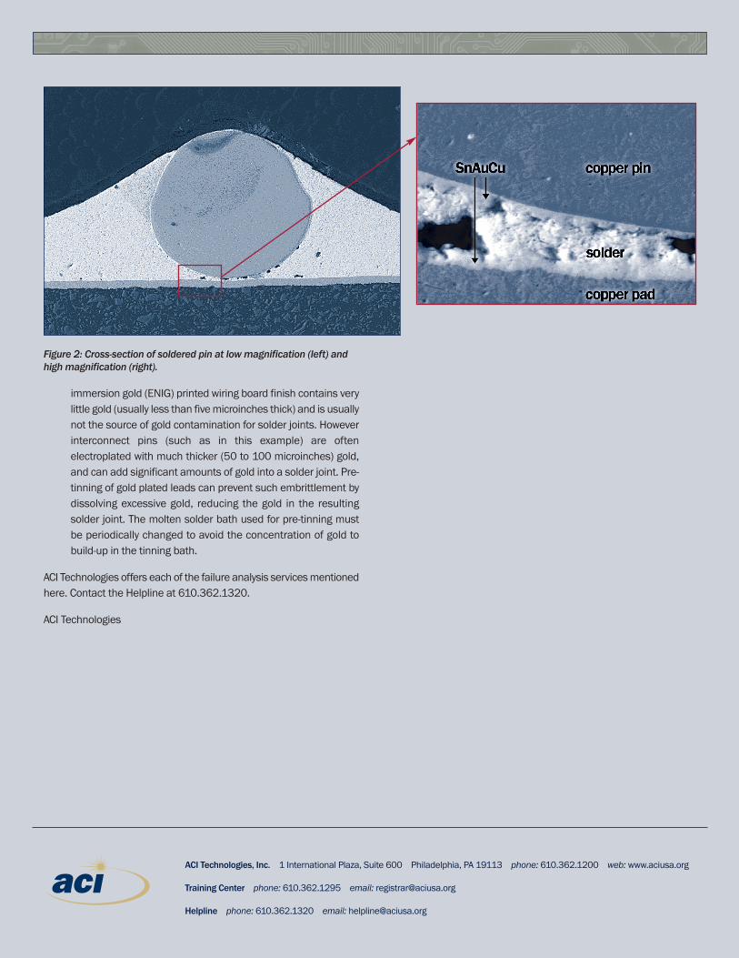
Figure 2 shows a cross-section of one of the soldered pins at low andhigh magnifications. The larger image on the left shows the pin padinterface at the bottom of the solder joint. SnAuCu intermetallic layerswere observed in the solder between the pin and the pad. Voids anddegradation were observed in the solder adjacent to theseintermetallic layers.
Conclusions
The separation of solder from the pin was caused by contaminationwith gold and lead intermetallic formations near the pin interface thatweakened the solder and caused premature joint failure.
Two precautions were indicated:
1. Lead contamination must be eliminated from the solderingoperation. Possible sources of lead contamination include thetip of the soldering iron or cross-contamination of the soldermaterials. The solder materials should be analyzed for contentand soldering tips must be cleaned and kept free of lead priorto soldering with lead-free solders.
2. Gold should be limited in the solder joint to avoid a conditioncalled gold embrittlement, where excessive gold content in thesolder reduces the number of thermal cycles a solder joint canendure. A gold concentration of 3% by weight is consideredenough excess gold to weaken a joint. Electroless nickel
continued on next page
ACI Technologies, Inc. 1 International Plaza, Suite 600 Philadelphia, PA 19113 phone: 610.362.1200 web: www.aciusa.org
Training Center phone: 610.362.1295 email: [email protected]
Helpline phone: 610.362.1320 email: [email protected]
Figure 2: Cross-section of soldered pin at low magnification (left) andhigh magnification (right).
immersion gold (ENIG) printed wiring board finish contains verylittle gold (usually less than five microinches thick) and is usuallynot the source of gold contamination for solder joints. Howeverinterconnect pins (such as in this example) are oftenelectroplated with much thicker (50 to 100 microinches) gold,and can add significant amounts of gold into a solder joint. Pre-tinning of gold plated leads can prevent such embrittlement bydissolving excessive gold, reducing the gold in the resultingsolder joint. The molten solder bath used for pre-tinning mustbe periodically changed to avoid the concentration of gold tobuild-up in the tinning bath.
ACI Technologies offers each of the failure analysis services mentionedhere. Contact the Helpline at 610.362.1320.
ACI Technologies