Ideal Tx-Line Reflection - 國立臺灣大學
67
Ideal Tx-Line Reflection 吳瑞北 Rm. 340, Department of Electrical Engineering E-mail: [email protected] google: rbwu S. H. Hall et al., High-Speed Digital Design, Chap.3 N. N. Rao, Elements of Engineering Electromagnetics, Chap. 6 1
Transcript of Ideal Tx-Line Reflection - 國立臺灣大學

Ideal Tx-Line Reflection
吳瑞北
Rm. 340, Department of Electrical Engineering
E-mail: [email protected]
google: rbwu
S. H. Hall et al., High-Speed Digital Design, Chap.3
N. N. Rao, Elements of Engineering Electromagnetics, Chap. 6 1

R. B. Wu
What will you learn?
• How to solve circuits with ideal lossless tx-line?
• Is there easier “analytic” equ. circuit model.
• How to solve “analytically” tx-line circuits with R,
L, and C loading/discontinuities?
• How does reflection come from? How to deal with
multiple reflection phenomenon?
• How to measure? Operation principle of TDR.
• How to extract tx-line parameters & discontinuities
from TDR measurement?
• How to mitigate reflection?2

R. B. Wu
Contents
• Analytic Tx-Line Analysis
• Reflections from Resistive Loads
• Reflection from Reactive Loads
• Time Domain Reflectometry
• Termination Designs
3

Analytic Tx-Line Analysis
4

R. B. Wu
Distributed Element
vS(t)
iA(t)
vB(t)
v(z,t)_
+
i(z,t)
i(z,t)
GROUND
vA(t)
iB(t)
Tx-line is also called
a distributed element
• vs. lumped elements ZS, ZL.
• Note the reference of V(z,t).
• Where is the ground of tx-line?
• I(z,t) must accompany the return-path current.
• How to interpret a negative I(z,t)?
• How to solve circuits with a distributed circuit element?
5

R. B. Wu
Eq. Circuit Model for SPICE Simulation
Rule of Thumb:
pr vt
10 segments of # Decide 1.
max freq.
segmentNote: TD 10 # 10
rt
#*GC,L,R, GC,L,R, Choose 2. segment

R. B. Wu
Equivalent Circuit Seen from Both Ends
tVtVZ
tItI
tVtVtVtV
A
A
0
1),0()(
),0()(
TtVTtVZ
tItI
TtVTtVtVtV
B
B
0
1),()(
),()(
pp
pp
vz
vz
vz
vz
tVtVZ
tzI
tVtVtzV
0
1),(
),(
Ref.: F. H. Branin, Jr., “Transient analysis of lossless transmission lines,” Proc. IEEE, vol. 55, pp.
2012-2013, Nov. 1967.
0( ) ( )
2 ( 0, )
2 ( , )
A AV t Z I t
V z t
V z t T
0( ) ( )
2 ( , )
2 ( 0, )
B BV t Z I t
V z t
V z t T
; B AV V V V V V
7

R. B. Wu
Circuit Modeling
Equivalent circuit
Time delay
Impedance
Rem: Only 4 lumped
elements, even for very
long tx-line.
A B
0; Z T
* voltage controlled voltage source
( ) 2 ( ) ( )
( ) 2 ( ) ( )
A B B
B A A
E t v t T E t T
E t v t T E t T
8
Z0
EA
VA
Z0
EB
VB

R. B. Wu
Z0
ZLEB (t) VB (t)
Zs Z0
Vs (t) EA (t)VA (t)
Time Marching
tx x 0 x 0 0 0
x x 0 x 0 0 0
x x 0 x 0 0 0
x x 0 x x x x
x x 0 x x x x
x x 0 x x x x
x x x x x x x
x x x x x x x
x x x x x x x
T
2T
3T
( ) 0S A A B BV t V (t) E (t) V ( ,t) V ( ,t) E (t) V (t)
9
At source end At load end

Reflections from Resistive Loads
10

R. B. Wu
Time-Domain Sol. w/o Simulator
1. Determine launch voltage & final “DC” or “t =0”
voltage
2. Calculate load reflection coefficient and voltage
delivered to the load
3. Calculate source reflection coefficient and
resultant source voltage
11

R. B. Wu
Determine Launch Voltage
Step 1: determine launch voltage
– Simply a voltage divider!
VsZo
RsVs
0
TD
Rt
A B
t=0, V=Vi
(initial voltage)
RSZ0
Z0VSVi
+=
RSRt
RtVSVf
+=
12
V +
I +
Rg
V0
Z = 0
I +
Rg
V0
Z = 0
Z0 V +

R. B. Wu
Z0
2Ei
VB
RL
Voltage Delivered to Load
VsZo
RsVs
0
TD
Rt
A B
t=0, V=Vi
t=TD, V=Vi + rB(Vi )
(signal is reflected)
(initial voltage)
Step 2: determine VB at t = TD− Tx-line delays the arrival of launched voltage until t = TD.
− VB for 0 < t < TD is at quiescent voltage (0 in this case)
− Voltage wavefront will be reflected at tx-line end
− VB = Vincident + Vreflected at t = TD
ZoRt
ZoRt
rB
Vreflected = rB (Vincident)
VB = Vincident + Vreflected 0
0
;2
ZVI
VVV
RZ
RVV
B
L
LB
dt for
13

R. B. Wu
IA
Rg
V0
Z = 0
VA
2Er
Z0
Voltage Reflected back to Source
VsZo
RsVs
0
TD
Rt
A B
t=0, V=Vi
t=TD, V=Vi + rB
(Vi )
t=2TD,
V=Vi + rB
(Vi) + rAr
B)(Vi )
(signal is reflected)
(initial voltage)
rA rB
14

R. B. Wu
Voltage Reflected Back to Source
Step 3: Determine VA at t = 2TD− Tx-line delays the arrival of voltage reflected from load
until t = 2TD.
− VA at time 0 < t < 2TD is at launch voltage
− Voltage wavefront will be reflected at source
− VA = Vlaunch + Vincident + Vreflected at t = 2TD
In steady state, sol. converges to VB = VS [Rt/(Rt + Rs)]
ZoRs
ZoRs
rA
Vreflected = rA (Vincident)
VA = Vlaunch + Vincident + Vreflected
15
R. B. Wu
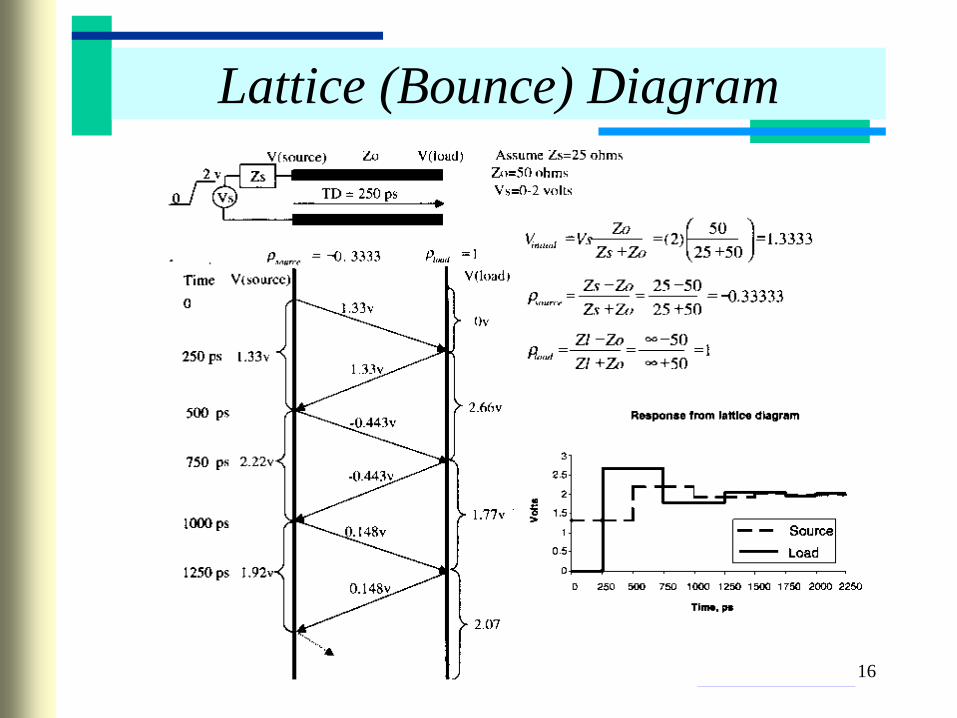
Lattice (Bounce) Diagram
16
R. B. Wu
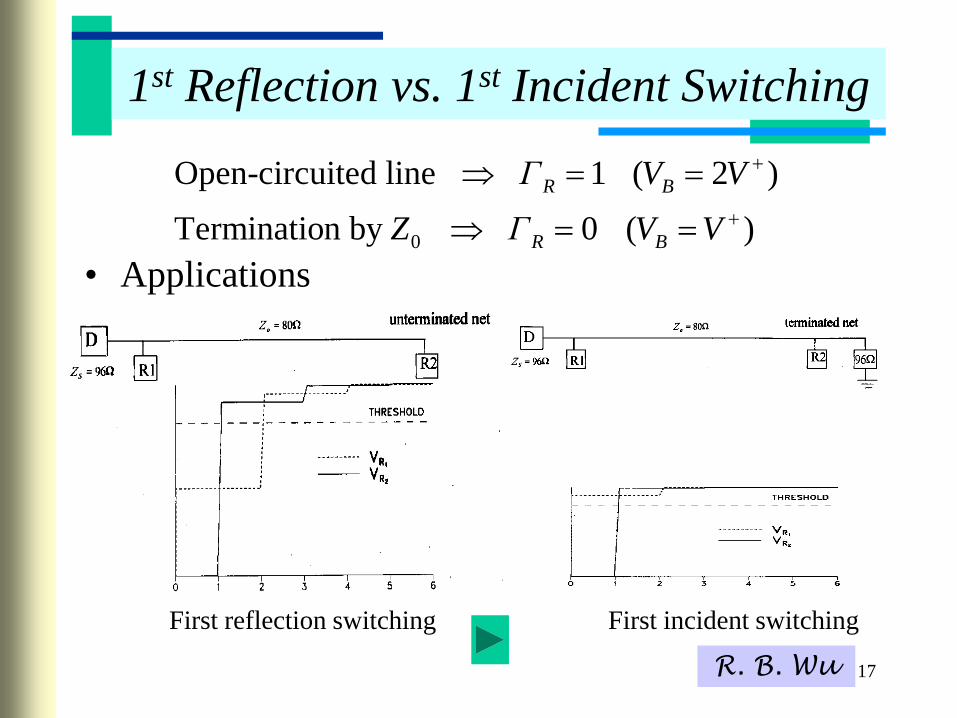
1st Reflection vs. 1st Incident Switching
• Applications 0
Open-circuited line 1 ( 2 )
Termination by 0 ( )
R B
R B
Γ V V
Z Γ V V
First incident switchingFirst reflection switching
17

R. B. Wu
Over Driven Tx-Line (Under Damped)
150
50
33333.05025
5025
3333.15025
50)2(
÷
ZoZl
ZoZl
ZoZs
ZoZs
ZoZs
ZoVsV
load
source
initial
r
r
Assume Zs=25 ohms
Zo =50ohms
Vs=0-2 voltsVs
Zs
ZoV(source) V(load)
TD = 250 ps0
2 v
Time V(source) V(load)
1.33v
3333.0source
r 1load
r
1.33v1.33v
-0.443v
0v
2.66v
1.77v
-0.443v2.22v
0.148v
0
500 ps
1000 ps
1500 ps
2000 ps
2500 ps 1.920.148v
2.07
Response from lattice diagram
0
0.5
1
1.5
2
2.5
3
0 250 500 750 1000 1250 1500 1750 2000 2250
Time, ps
Vo
lts
Source
Load
18
R. B. Wu
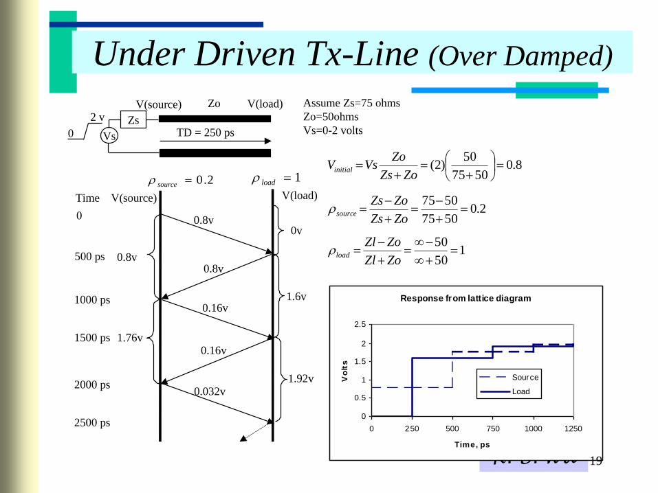
Under Driven Tx-Line (Over Damped)
Assume Zs=75 ohms
Zo=50ohms
Vs=0-2 voltsVs
Zs
ZoV(source) V(load)
Time V(source) V(load)
150
50
2.05075
5075
8.05075
50)2(
ZoZl
ZoZl
ZoZs
ZoZs
ZoZs
ZoVsV
load
source
initial
r
r0.8v
2.0sourcer 1loadr
0.8v0.8v
0.16v
0v
1.6v
1.92v
0.16v1.76v
0.032v
TD = 250 ps
0
500 ps
1000 ps
1500 ps
2000 ps
2500 ps
0
2 v
Response from lattice diagram
0
0.5
1
1.5
2
2.5
0 250 500 750 1000 1250
Time, ps
Vo
lts
Source
Load
19

R. B. Wu
Effects of Rise Time – overdriven case
20

R. B. Wu
Effects of Rise Time – underdriven case
21

R. B. Wu
Reflection and Transmission
r
1rIncident
Reflected
Transmitted
0
0
Reflection Coefficient
t
t
Z Z
Z Zr
0
0
0
=1+ 1
Transmission Coefficient
2
t
t
t
t
Z Z
Z Z
Z
Z Z
r
22

R. B. Wu
Multiple line impedance
23

R. B. Wu 24

R. B. Wu
Multi Receivers Topology
Eig 3-35
0
1 3
2
50
250 ;
125 ;
sZ R
l l ps
l ps
0 0 12 3
0 0
22 2 3
1 23 33 3
4 5
2
2
1
;
1; 1
Z Z
Z Z
T
T
43
89
5227
v
v
v
43
209
A
B
v
v
25
Rs=Zs
0-2V
Receiver 1
l3 > l2
Receiver 2
l2
l1
Z0
Z0
Z0

R. B. Wu
Effects of Non-symmetry
26
Rs=Zs
0-2V
Receiver 1
l3 > l2
Receiver 2
l2
l1
Z0
Z0
Z0

R. B. Wu
Ringing Noise on Address Lines of DDR
27
Short End
Long End
Z0L1=(Lt-Δl)/2
0-1.5V
L3
Tr=200psL2=(Lt+Δl)/2
Z0, vp, Rs, tanD
8
3
4 1
3
/ 2.5; 3.27
tanD 0.02
3 10 10
ps; / 100
/ 21 s;4p /
p s
p
t p pt
R s m
L v
T L v
v
TD
t l v
0 0.5 1 1.5 2 2.5 3-0.5
0
0.5
1
1.5
2
Ringing Effect
Volt
age(
V)
time(ns)
l/Lt=0
l/Lt=0.2, Short End
l/Lt=0.2, Long End
l/Lt=0.4, Short End
l/Lt=0.4, Long End
0 0.5 1 1.5 2 2.5 3-0.5
0
0.5
1
1.5
2
Ringing Effect
Volt
age(
V)
time(ns)
l/Lt=0.6, Short End
l/Lt=0.6, Long End
l/Lt=0.8, Short End
l/Lt=0.8, Long End

R. B. Wu
RLC Resonance Model of Ringing Noise
• The total response can be divided into the balanced response and the ringing
noise response.
• The ringing noise response can be fitted as a RLC resonance response
28
0 0.5 1 1.5 2 2.5 3-0.5
0
0.5
1
1.5
2
Step Response, l/Lt=0.12
Volt
age(
V)
time(ns)
Balanced
Precise, short end
Model, short end
Precise, long end
Model, long end
Ringing
Z0
0-1.5V
Tr=200ps
Z0, L3 Z0/2
v0
L
0-1.5VTr=200ps
vstep(t-TD)
TD=L3/vp
vn
v0
Avn
veq
0eq nv v v
2
0
sin2
sin2
t
t
t
l
LA
lL
L
2
0
sin2
2
t
p
t
l
Lbv
T
0
tT
j 1
0 0 0.884m
Equivalent
responseBalanced
response
Ringing noise
response

R. B. Wu
0 00
0
0.2 0.20.2
0.20.2
0.4
0.40.4
0.4 0.4
0.40.40.6
0.6 0.6
0.6
0.60.6
0.6
0.6
0.60.6
0.6
0.8
0.8
0.8
0.8
Eye Height/Vh
l/Lt
UI/
Tt
0 0.1 0.2 0.3 0.4 0.5 0.61
2
3
4
5
6
7
Eye Height – Bit rate Influence
• Worst case occurs at UI/Tt is odd.
29
65%
0%
UI/Tt=4, Δl/Lt=0.12
UI/Tt=3, Δl/Lt=0.12

R. B. Wu
0%
UI/Tt=3, Δl/Lt=0.12
Eye Height – Leg Difference Influence
• Worst case occurs
at where the max
of A occurs.
30
0 00
0
0.2 0.20.2
0.20.2
0.4
0.40.4
0.4 0.4
0.40.40.6
0.6 0.60.6
0.60.6
0.6
0.6
0.60.6
0.6
0.8
0.8
0.8
0.8
Eye Height/Vh
l/Lt
UI/
Tt
0 0.1 0.2 0.3 0.4 0.5 0.61
2
3
4
5
6
7
62%
UI/Tt=3, Δl/Lt=0.6
0 0 122
.t
lL
L
Ref: K.-Y. Yang, et al., “Modeling and
fast eye- diagram estimation of ringing
effects on branch line structures,” IEEE
T-CPMT, Apr. 2014.

R. B. Wu
Effect of a Long Stub
31

Reflections from Reactive Loads
32

R. B. Wu
V0
v(l,t)
V0 / 2
zz = z1 z = l
Inductive Termination
R0
V0
z = 0
t=0
z = lz = z1
LL
V0 / 2
R0
iL(t)
2v+(0, t-T)
R0
LLv(l,t)
V0
v(l,t)
0RLLT t
0(0, ) 2v t V
0tfor
for t T l u
0 0
0
0
0 0
( )
( )
0
2
( ) 1
( ) ( , )
L
L
LL L
V t T R L
L R
t T R L
L
diL R i v V
dt
i t e
v t v l t V e
0( , ) ( , ) 2v l t v l t V
2for T t T
1z l u t T
R. B. Wu
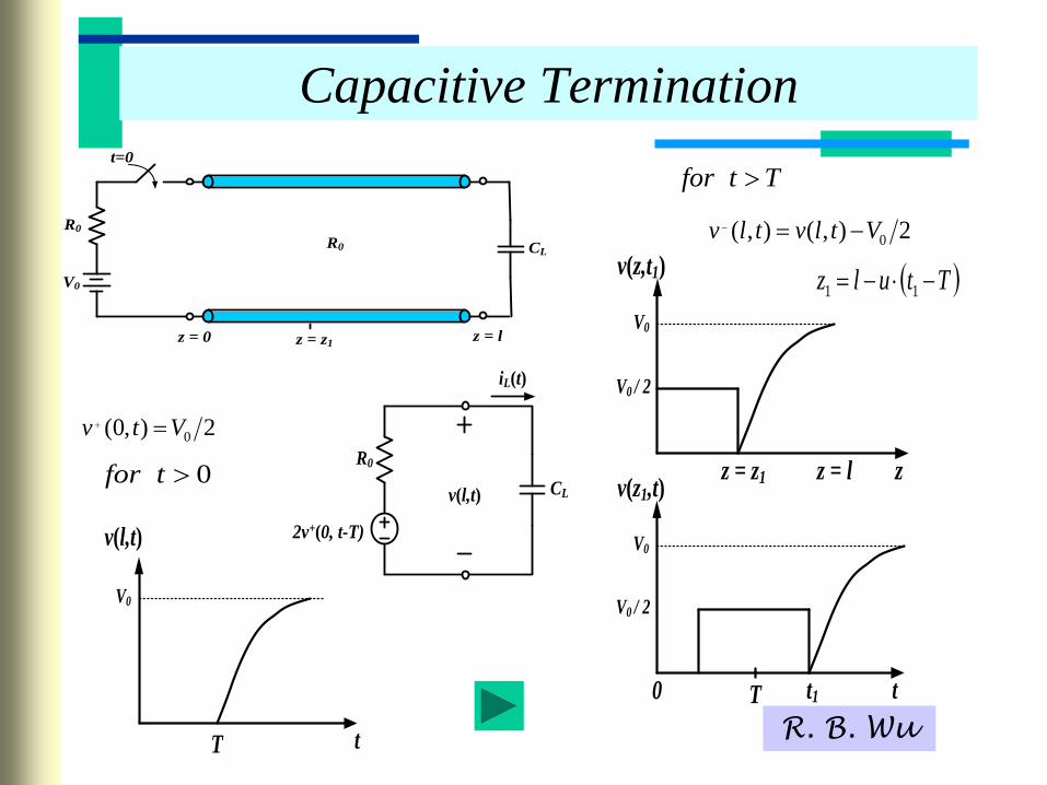
Capacitive Termination
R0
V0
t=0
CLR0
z = 0 z = lz = z1
iL(t)
2v+(0, t-T)
R0
v(l,t) CL
V0
v(l,t)
T t
V0
v(z1,t)
V0 / 2
tt1T0
V0
v(z,t1)
V0 / 2
zz = z1 z = l0tfor
Ttfor
0( , ) ( , ) 2v l t v l t V
Ttulz 11
0(0, ) 2v t V

Time Domain Reflectometry
36

R. B. Wu
Time-Domain Reflectometry
• Key advantages over frequency measurement
– Ability to extract electrical data relevant to digital systems
– Can extract impedance, velocity, tx-line parameters, and model
parameters of discontinuities.
• Basic theory
oDUT
oDUT
oDUT
ZZ
ZZ
V
V
ZZ
incident
reflected
;1
1
r
r
r
37

R. B. Wu
Impedance & Velocity
at
no
de
A
38

R. B. Wu
Peeling Idea for Reflections
• Multiple reflections.
• Need minimize reflections prior to DUT & TDR
– Use a controlled-impedance, low-loss cable btw TDR & probe
– Use a low-loop-inductance, controlled-impedance probe
J. M. Jong and V. K.
Tripathi, IEEE T-CHMT,
pp. 497-504, Aug .
1992
J. M. Jong, B. Janko
and V. K. Tripathi,
IEEE T-CHMT, pp.
119-126, Feb. 1993
41

R. B. Wu
Inductive Load in Middle of a Line
42
02
max
0
12
rZ t
L
r
Le
t Zr
ind
0
;4
sv LA
Z
vs: excitation voltage
vs

R. B. Wu
Capacitive Load in Middle of a Line
Vr
Tw,50
CD
VB-Ei
43
0cap ;
4
sv Z CA

R. B. Wu
Discontinuity Loading
44

R. B. Wu
Equally Spaced Capacitive Loads
nst
pFC
ns
Z
r
L
d
35.0
2
573.0
7.490
45
R. B. Wu
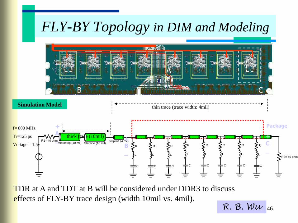
R1= 40 ohmStripline (10 mil)
R2= 40 ohm
stripline (4 mil)
C
R
C
R
C
R
C
R
C
R
C
R
C
R
C
R
L L L L L L L L
Microstrip (10 mil)
+A _
Simulation Model
f= 800 MHz
Tr=125 ps
Voltage = 1.5v
Package
thin trace (trace width: 4mil)
thick trace (10mil)+B _
+C _
B C
A
TDR at A and TDT at B will be considered under DDR3 to discuss
effects of FLY-BY trace design (width 10mil vs. 4mil).
FLY-BY Topology in DIM and Modeling
46

R. B. Wu
Simulation
Results
0 1 2 3 4 5 6
Time (nSec)
0
0.2
0.4
0.6
0.8
1
Vol
tage
(V
)
Trace Width = 4 mil
Trace Width = 10 mil
0 1 2 3 4 5 6
Time (nSec)
0
0.2
0.4
0.6
0.8
1
Vol
tage
(V
)
Trace Width = 4 mil
Trace Width = 10 mil
TDR TDT
Suitable trace width (thin trace) improves impedance match.
R1= 40 ohmStripline (10 mil)
R2= 40 ohm
stripline (4 mil)
C
R
C
R
L L
Microstrip (10 mil)
+B _
A
f= 800 MHz
Tr=125 ps
trace width
AV BV
H.-H. Chuang, et al., “Signal/power integrity modeling of high-speed memory
modules using chip-package-board co-analysis,” IEEE T-EMC, May 2010. 47
R. B. Wu
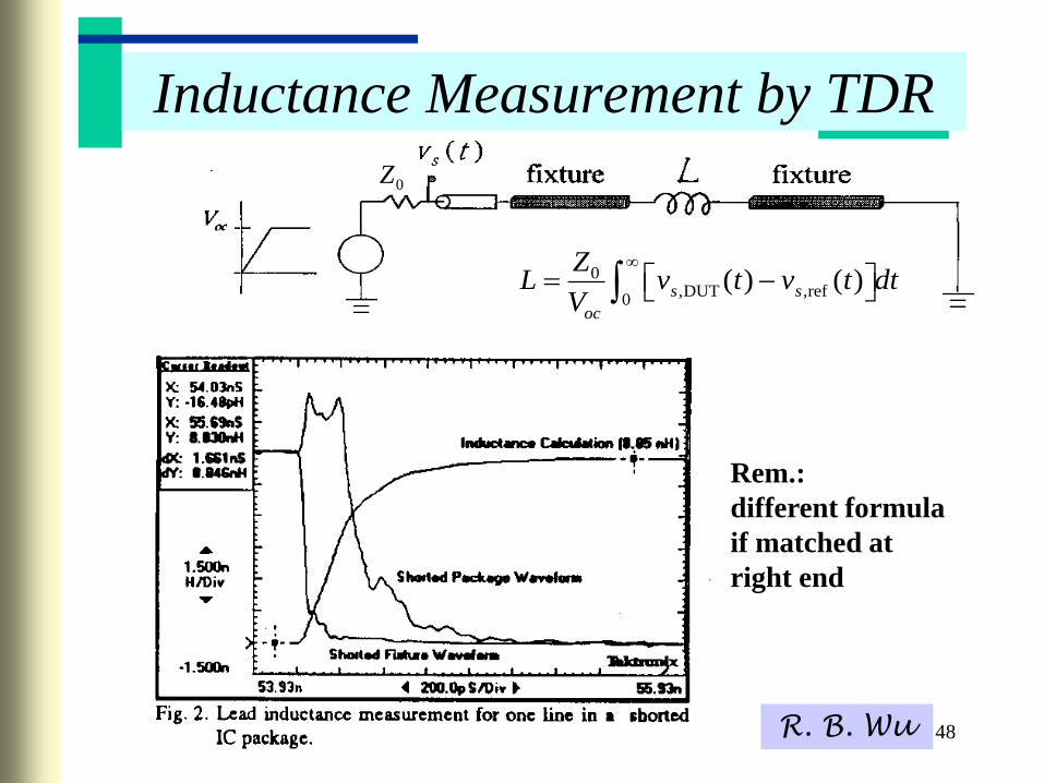
Inductance Measurement by TDR
0,DUT ,ref
0( ) ( )s s
oc
ZL v t v t dt
V
0Z
Rem.:
different formula
if matched at
right end
48

R. B. Wu
Capacitance Measurement by TDR
0Z
,ref ,DUT0
0
1( ) ( )o o
oc
C v t v t dtZ V
49

Termination Design
50

R. B. Wu
Termination Schemes to minimize reflection noise
• Decrease system frequency
• Shorten PCB traces
• Termination with matched impedance
– Source termination
• On-die source termination
• Series source termination
– Parallel termination (Load termination)
• Load termination with a resistive load
• AC load termination
• Active termination
Ref.: H. Johnson & M. Graham, High-Speed Digital Design, Sec.6.1-4 51

R. B. Wu
Source Termination
• On-die source termination
• Series source termination
Difficult to guarantee matched buffer impedance!
Add cost to board, and consumes board area!
52
R. B. Wu
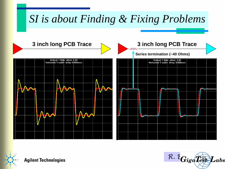
SI is about Finding & Fixing Problems
3 inch long PCB Trace3 inch long PCB Trace
Series termination (~40 Ohms)
53

R. B. Wu
Source Termination
2(Pulse Freq.)Power
2
f DDV
R
21
E 22
DDf
V
R
CZT RC 090-10 2.22.2
overshoot
:suggested
0
ZRR ops
54

R. B. Wu
Load Termination
• Load termination with a resistive load
• AC load termination
Power delivery and thermal problems!
Capacitor value need be optimized for specific design
Capacitive loading increases signal delay! 55

R. B. Wu
Load Termination
CD
CZZRC
T
L
RC
00
term.
1.1)//(2.2
2.2
22
term:risetimenet rtT
Too much power consumption!
Eq. ckt
56

R. B. Wu
Split Termination
021 // match ZRR
0
2
1
22
2
22
2
)(
2
)()(
2
)()(
load
P
Z
V
R
VVVV
R
VVVV
LOCCHICC
EELOEEHI
57

R. B. Wu
Load Termination for Multiple Lines
Cap. of each
short stub adds
to cap. load of
receiver
• Daisy-chain configuration
End termination
• Bifurcated line
with matched
trace impedance
58

R. B. Wu
AC Load Termination
• Power saving (in DC-balanced circuit)
0
2
0
2
1 4
)()2/(
RPZ
V
Z
V
clock time1 CR
59

R. B. Wu
Concept of Load-Line Analysis

R. B. Wu
Tx-Line Bergeron-Plot Analysis
0
0
( ) ( ) 2 ( )
2 ( , )
( ) ( )
A A
B B
V t Z I t g t
V z t T
V t T Z I t T
0
0
( ) ( ) 2 ( )
2 ( 0, )
( ) ( )
B B
A A
V t Z I t f t T
V z t T
V t T Z I t T
• Easily applicable for nonlinear resistive load
AssA IRVV
BLB IRV

R. B. Wu
A Practical Example

R. B. Wu
Voltage Waveform at Transition
Voltage waveform at the receiving end of Tx-line
Low to high High to low

R. B. Wu
Match by Series Termination

R. B. Wu
Match by Parallel Termination
new

R. B. Wu
Active Termination
67
50 Ω
25 Ω1
2/3
25 ΩV L H
V L H
TTL / CMOS
Clamp to -1V on HIGH-to-LOW (limit signal undershoot)
Suitable for any Z0
Power saving
L L L
L L R0
Voo
L
Vbb
0.1 μF
ECL

R. B. Wu
Comparisons
• Rise time of an end-terminated circuit, when capacitively
loaded, is half of a series-terminated line driving same load.
• Most TTL or CMOS gates can’t source enough current to
drive end terminators. Split termination or capacitive
termination can be a remedy.
• One can daisy-chain receivers on an end-terminated line.
• At low-pulse repetition rates, source terminations dissipates
little power.
• Peak drive power for source-terminated line is
same as end-terminated line (biased at halfway point) R
V 1
2
2
68

R. B. Wu
Did you learn?
• What’s diff. of “distributed” from “lumped” circuits?
• How to solve “analytically” tx-line circuits with R,
L, and C loading/discontinuities?
• Load & source reflection coeff. & bounce diagram.
• Operation principle of time domain reflectometry.
• How to extract tx-line parameters & discontinuities
from TDR measurement?
• How to mitigate reflection?
69

R. B. Wu
References & Further Reading
• F. H. Breanin, Jr., “Transient analysis of lossless transmission lines,”
IEEE Proc. Lett., pp.2012-2013, 1967.
• J. M. Jong, B. Janko, and V. K. Tripathi, “Equivalent circuit modeling of
interconnects from time-domain measurements,” IEEE T-CHMT, vol. 16,
pp. 119-126, Feb. 1993.
• M.-H. Wang and R.-B. Wu, “Measuring method for equivalent
circuitry,” USA Patent 6,137,293, Oct. 2000.
• H.-H. Chuang, et al., “Signal/power integrity modeling of high-speed
memory modules using chip-package-board coanalysis,” IEEE T-EMC,
vol. 52, pp. 381-391, May 2010.
• K.-Y. Yang, et al., “Modeling and fast eye-diagram estimation of ringing
effects on branch line structures,” IEEE T-CPMT, Apr. 2014.
• A. Boutar, et al., "An efficient analytical method for electromagnetic
field to transmission line coupling into a rectangular enclosure excited by
an internal source", IEEE T-EMC, pp. 1-9, 2015.70

R. B. Wu
References & Further Reading
• A. Beygi and A. Dounavis, "Analysis of excited multi-conductor
transmission lines based on the passive method of characteristics
macro-model," IEEE T-EMC, vol. 54, pp. 1281 - 1288 , Dec. 2012.
• F. Capolino, et al., "Equivalent transmission line model with a lumped
X-circuit for a meta-layer made of pairs of planar conductors,” IEEE
T-AP, vol. 61, pp. 852-861, Feb. 2013.
• G. Lugrin, et al., "High-frequency electromagnetic coupling to multi-
conductor transmission lines of finite length,” IEEE T-EMC, vol. 57,
pp. 1714-1723, Dec. 2015.
• M. Chernobryvko, D. De Zutter, and D. Vande Ginste, "Nonuniform
multi-conductor transmission line analysis by a two-step perturbation
technique", IEEE T-CPMT, vol. 4, pp. 1838-1846, Nov. 2014.
• G. Antonini, et al., "Review of Clayton R. Paul studies on multi-
conductor transmission lines", IEEE T-EMC, vol. 55, pp. 639-647,
Aug. 2013.
71