iC-PVL EVAL PVL1M · J1-15 DI_P1 Multiturn Interface, Data Input, Parallel Output Bit 1 (positive...
12
preliminary preliminary iC-PVL EVAL PVL1M EVALUATION KIT DESCRIPTION Rev A1, Page 1/12 ORDERING INFORMATION Type Order Designation Description Options Evaluation Kit iC-PVL EVAL PVL1M iC-PVL Evaluation Board Ready-to-operate, supplied with magnetic code disc and BiSS adapter cable Evaluation Software iC-PVL GUI GUI Software for Windows PC Device setup file generation, board configuration via adapter For download link check www.ichaus.de/pvl_gui Related parts (to be ordered separately) PC Adapter iC-MB3 iCSY MB3U-I2C PC-USB adapter for BiSS/SSI w. I2C/SPI extension cable Download documentation at www.ichaus.com/tools BOARD PVL1M (size 61 mm x 64 mm) PLUG CONFIGURATION Figure 1: Component side J1 Signal Connector J2 SSI Interface (to PC adapter via BiSS adapter cable) J3 I 2 C Interface (to PC adapter I 2 C exten- sion cable) Copyright © 2016 iC-Haus http://www.ichaus.com
Transcript of iC-PVL EVAL PVL1M · J1-15 DI_P1 Multiturn Interface, Data Input, Parallel Output Bit 1 (positive...

preliminary
preliminary iC-PVL EVAL PVL1MEVALUATION KIT DESCRIPTION
Rev A1, Page 1/12
ORDERING INFORMATION
Type Order Designation Description Options
Evaluation Kit iC-PVL EVAL PVL1M iC-PVL Evaluation BoardReady-to-operate, supplied with magnetic code disc and BiSS adaptercable
Evaluation Software iC-PVL GUI GUI Software for Windows PCDevice setup file generation, board configuration via adapterFor download link check www.ichaus.de/pvl_gui
Related parts (to be ordered separately)PC Adapter iC-MB3 iCSY MB3U-I2C PC-USB adapter for BiSS/SSI w. I2C/SPI extension cable
Download documentation at www.ichaus.com/tools
BOARD PVL1M
(size 61 mm x 64 mm) PLUG CONFIGURATION
Figure 1: Component side
J1 Signal Connector
J2 SSI Interface (to PC adapter via BiSSadapter cable)
J3 I2C Interface (to PC adapter I2C exten-sion cable)
Copyright © 2016 iC-Haus http://www.ichaus.com
preliminary
preliminary iC-PVL EVAL PVL1MEVALUATION KIT DESCRIPTION
Rev A1, Page 2/12
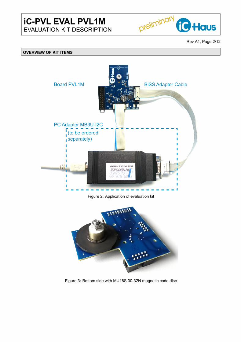
OVERVIEW OF KIT ITEMS
Figure 2: Application of evaluation kit
Figure 3: Bottom side with MU18S 30-32N magnetic code disc
preliminary
preliminary iC-PVL EVAL PVL1MEVALUATION KIT DESCRIPTION
Rev A1, Page 3/12
RELATED PRODUCTS AND DOCUMENTS
• IC Documentation→ http://www.ichaus.de/PVL
• PC-USB Adapter Description→ http://www.ichaus.de/MB3U_MB3U-I2C_datasheet_en
• GUI Software for Windows PC: check here for down-load links→ http://www.ichaus.de/PVL
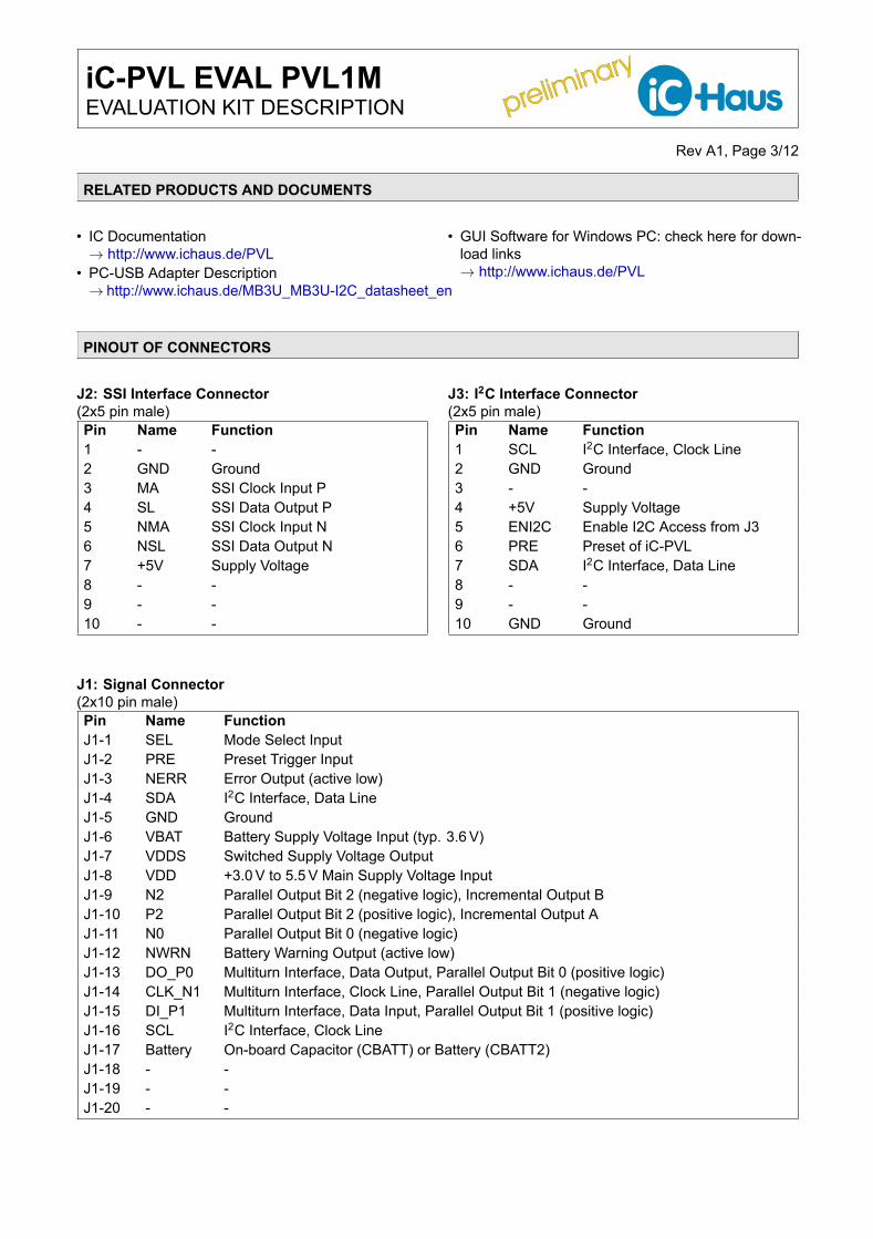
PINOUT OF CONNECTORS
J2: SSI Interface Connector(2x5 pin male)Pin Name Function1 - -2 GND Ground3 MA SSI Clock Input P4 SL SSI Data Output P5 NMA SSI Clock Input N6 NSL SSI Data Output N7 +5V Supply Voltage8 - -9 - -10 - -
J3: I2C Interface Connector(2x5 pin male)Pin Name Function1 SCL I2C Interface, Clock Line2 GND Ground3 - -4 +5V Supply Voltage5 ENI2C Enable I2C Access from J36 PRE Preset of iC-PVL7 SDA I2C Interface, Data Line8 - -9 - -10 GND Ground
J1: Signal Connector(2x10 pin male)Pin Name FunctionJ1-1 SEL Mode Select InputJ1-2 PRE Preset Trigger InputJ1-3 NERR Error Output (active low)J1-4 SDA I2C Interface, Data LineJ1-5 GND GroundJ1-6 VBAT Battery Supply Voltage Input (typ. 3.6 V)J1-7 VDDS Switched Supply Voltage OutputJ1-8 VDD +3.0 V to 5.5 V Main Supply Voltage InputJ1-9 N2 Parallel Output Bit 2 (negative logic), Incremental Output BJ1-10 P2 Parallel Output Bit 2 (positive logic), Incremental Output AJ1-11 N0 Parallel Output Bit 0 (negative logic)J1-12 NWRN Battery Warning Output (active low)J1-13 DO_P0 Multiturn Interface, Data Output, Parallel Output Bit 0 (positive logic)J1-14 CLK_N1 Multiturn Interface, Clock Line, Parallel Output Bit 1 (negative logic)J1-15 DI_P1 Multiturn Interface, Data Input, Parallel Output Bit 1 (positive logic)J1-16 SCL I2C Interface, Clock LineJ1-17 Battery On-board Capacitor (CBATT) or Battery (CBATT2)J1-18 - -J1-19 - -J1-20 - -
preliminary
preliminary iC-PVL EVAL PVL1MEVALUATION KIT DESCRIPTION
Rev A1, Page 4/12
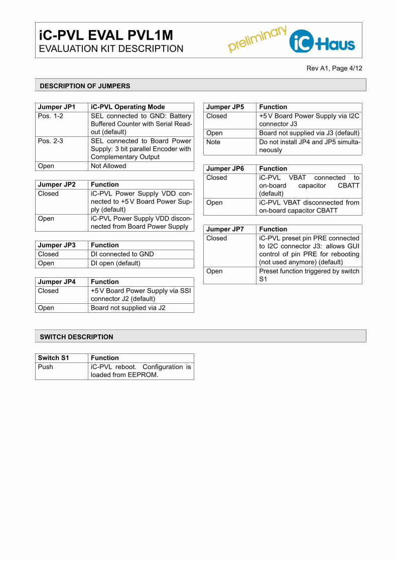
DESCRIPTION OF JUMPERS
Jumper JP1 iC-PVL Operating ModePos. 1-2 SEL connected to GND: Battery
Buffered Counter with Serial Read-out (default)
Pos. 2-3 SEL connected to Board PowerSupply: 3 bit parallel Encoder withComplementary Output
Open Not Allowed
Jumper JP2 FunctionClosed iC-PVL Power Supply VDD con-
nected to +5 V Board Power Sup-ply (default)
Open iC-PVL Power Supply VDD discon-nected from Board Power Supply
Jumper JP3 FunctionClosed DI connected to GNDOpen DI open (default)
Jumper JP4 FunctionClosed +5 V Board Power Supply via SSI
connector J2 (default)Open Board not supplied via J2
Jumper JP5 FunctionClosed +5 V Board Power Supply via I2C
connector J3Open Board not supplied via J3 (default)Note Do not install JP4 and JP5 simulta-
neously
Jumper JP6 FunctionClosed iC-PVL VBAT connected to
on-board capacitor CBATT(default)
Open iC-PVL VBAT disconnected fromon-board capacitor CBATT
Jumper JP7 FunctionClosed iC-PVL preset pin PRE connected
to I2C connector J3: allows GUIcontrol of pin PRE for rebooting(not used anymore) (default)
Open Preset function triggered by switchS1
SWITCH DESCRIPTION
Switch S1 FunctionPush iC-PVL reboot. Configuration is
loaded from EEPROM.

preliminary
preliminary iC-PVL EVAL PVL1MEVALUATION KIT DESCRIPTION
Rev A1, Page 5/12
CIRCUIT SCHEMATIC
VDD2: Board power supply
Power supplyvia I2C
Presetvia I2C
DI=GND
Preset
SEL
Connect Batteryto VBAT pin
ERROR
WARNING
POWER SUPPLY
VDD: PVL power supply
U4-A65LBC179A
7
82
120ΩR9
65LBC179A
DIFF_DRIVER
U4-B
36
5
DIFF_RECEIVER
J113
J114
J115
J116
9
J110
J111
J112
20 J28
J18
J1
7
CBATT20.9Ah
J1
J14
J15
J16
J1
J119
J12
J13
1
9 J31
J118
J33
J34
U3-ATS5A23157
210
10kΩR7
J27
560ΩR8
JP2
10
GND4
J24
J25
J26
J3
24XX_WP
U2-A24LC16B
1 SCL
3 SDA
WP5
J11
R110kΩ
46
5
7
RDD2
TS5A23157U3-S
GND3
VP8
TS5A23157U3-B
JP1
R4560Ω
JP8
JP3
U4-S
4GND
VCC1
C6100nF
C2100nF
65LBC179A
0.1FCBATT
100nFC1
J21
J22
J23
J29
JP7
1.5kΩ
D1OR
VDD
VDDS7
1.5kΩR2 R3
9N2
3NERR
NWRN 12
10P22 PRE
16SCL4SDA
SEL1
SUBEPAD
6VBAT
8
2
SIN/DIG CONVERTER
S/PO
LOGIC
SSI
U1
iC-PVL_SUB
iC-PVL
14CLK_N1
15 DI_P1 13DO_P0
5GND
11N0
R60Ω
J3
C5100nF
1
2
J210
JP4
JP6
D31N4148
6
J37
J38
J39
S1B3U-1000P-B S1
J35
J3
JP5
J117
GND2
VDD4
560ΩR5
C4100nF24LC16B
U2-S
VDD2
SDA
VDD2
VDD2
PRE
DO_P0
CLK_N1
VDD2
GND
Battery
1μFC3
N0
N2
P2
VDD2
VDD2
VDD2
VDD2 VDD2
VDD2
VDD2
VDD2
VDD2
SEL
NERR
VDDS
VDD
VDD
NWRN
DI_P1
VBAT
SCL
J2
J1
J1
J1
J1
J1
J1
J1
J1
J1
U4-B
DIFF_DRIVER
65LBC179A
65LBC179AU4-A
DIFF_RECEIVER
R9120Ω
J2
J2
J2
J3
D4GN
R8560Ω
JP2
R710kΩ
J2
J3
J3
TS5A23157U3-A
J3
J1
J1
J1
J1
J1
J1
J1
J1
0.9AhCBATT2
J1
ORD1
J2
JP7
J2
J2
J2
CBATT0.1F C1
100nF
100nFC2
U4-S65LBC179A 100nF
C6
JP8
JP3
JP1
560ΩR4
U3-STS5A23157
U3-BTS5A23157
D2RD
J1
10kΩR1
24LC16BU2-A
24XX_WP
C31μF
100nFC4U2-S
24LC16B
R5560Ω
JP5
J1
S1B3U-1000P-BS1
J3
J3
J3
J3
J3
JP6
1N4148D3
100nFC5
J2
JP4
0ΩR6
J3
B
B
B
B
iC-PVL
iC-PVL_SUB
U1
SSI
LOGIC
S/PO
SIN/DIG CONVERTER
R21.5kΩ 1.5kΩ
R3
Figure 4: Circuit diagram (board PVL1MZ)
preliminary
preliminary iC-PVL EVAL PVL1MEVALUATION KIT DESCRIPTION
Rev A1, Page 6/12
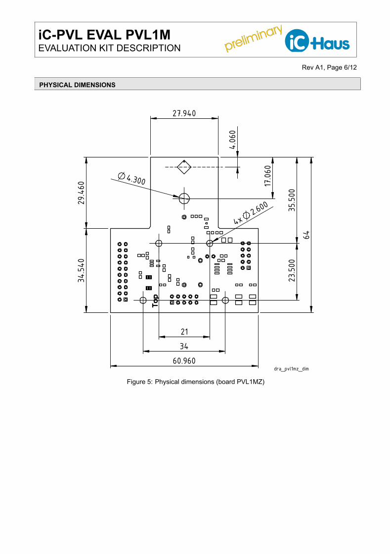
PHYSICAL DIMENSIONS 2
9.46
0 3
4.54
0
23.50
0
4x2.60
0
4.300
64
35.50
0 17.06
0
27.940
21
34
60.960
4.060
dra_pvl1mz_dim
Figure 5: Physical dimensions (board PVL1MZ)

preliminary
preliminary iC-PVL EVAL PVL1MEVALUATION KIT DESCRIPTION
Rev A1, Page 7/12
ASSEMBLY PART LIST
Figure 6: PCB (top side) Figure 7: PCB (bottom side)
Device Value (typical) CommentU1 iC-PVL Linear/off-axis hall-multiturn encoder ICU2 24AA02 Serial EEPROMU3 TS5A23157 Dual analog MUXU4 SN65LBC179A Differential line driver/receiverR1, R7 10 kΩ Pull-down resistorR2, R3 1.5 kΩ I2C pull-up resistorR4, R5, R8 560Ω LED series resistorR9 120Ω Line termination resistorJP1, JP2, JP4, JP7,R6
0 0Ω resistor
D1 LO-T67K Indicator LED for warning message (orange)D2 LS-T67K Indicator LED for error message (red)D3 1N4148WS Series diode for CBATT voltage reductionD4 LG-T67K Indicator LED for board power supply (green)C1, C2, C4, C5, C6 100 nF Supply backup capacitorC3 1 uF Supply backup capacitorCBATT 100 mF Capacitor for iC-PVL battery-buffer evaluationJ1 WSL20G Signal connectorJ2 WSL10G SSI interface (to PC adapter via BiSS adapter cable)J3 WSL10G I2C connector (to PC adapter I2C extension cable)S1 B3U-1000P-B Preset switch

preliminary
preliminary iC-PVL EVAL PVL1MEVALUATION KIT DESCRIPTION
Rev A1, Page 8/12
EVALUATION SOFTWARE
iC-PVL software for PCs running on Windows operating systems as well as the required USB driver are availableas a ZIP file. iC-Haus software built with LabVIEW™ requires the installation of the LabVIEW™ Run-Time Engine(RTE). The RTE must be installed only once, hence there are two download links available.
Software overview online: http://www.ichaus.de/software
Download package without RTE (small size) including RTE (big size)iC-PVL: http://www.ichaus.de/PVL_gui http://www.ichaus.de/PVL_gui_rte
Features• IC configuration made easy by parameter tables and tool tips• Editing of application-specific default setups (*.hex) with CRC calculation• Access to DUT and transfer of setup data to RAM and/or EEPROM• Storage of IC setups as Intel Hex file for programming devices
Installation
After unzipping the iC-PVL software package PVL1SO_gui_xx resp. PVL1SO_gui_xxrte, the following files arelocated in the selected working directory (xx is a placeholder for revisions):
→ Subfolder PVL1SO_gui_xx including the executable setup.exe which starts the installation routine.→ Driver package for USB adapter.
Notice: Administrator rights are required to run installations.
1. To access the iC-PVL evaluation board, interface adapter drivers for USB and/or other adapter devices need tobe installed. The driver installation must be completed successfully before connecting the adapter to your PC.→ Execute the USB_xx.exe installation package and follow the on-screen instructions. This can take a fewminutes.
1.1 To complete the driver installation procedure, the PC adapter must be connected to USB finally, after driverinstallation (only required if the adapter will be used).
2. Install the evaluation software PVL1SO by executing the setup.exe located in the subfolder PVL1SO_gui_xx.→ Follow the on-screen instructions to finish the installation.
3. After installation the executable PVL1SO_gui_xx.exe will be available in the selected working directory.
LabVIEW™ is a trademark of National Instruments.
preliminary
preliminary iC-PVL EVAL PVL1MEVALUATION KIT DESCRIPTION
Rev A1, Page 9/12
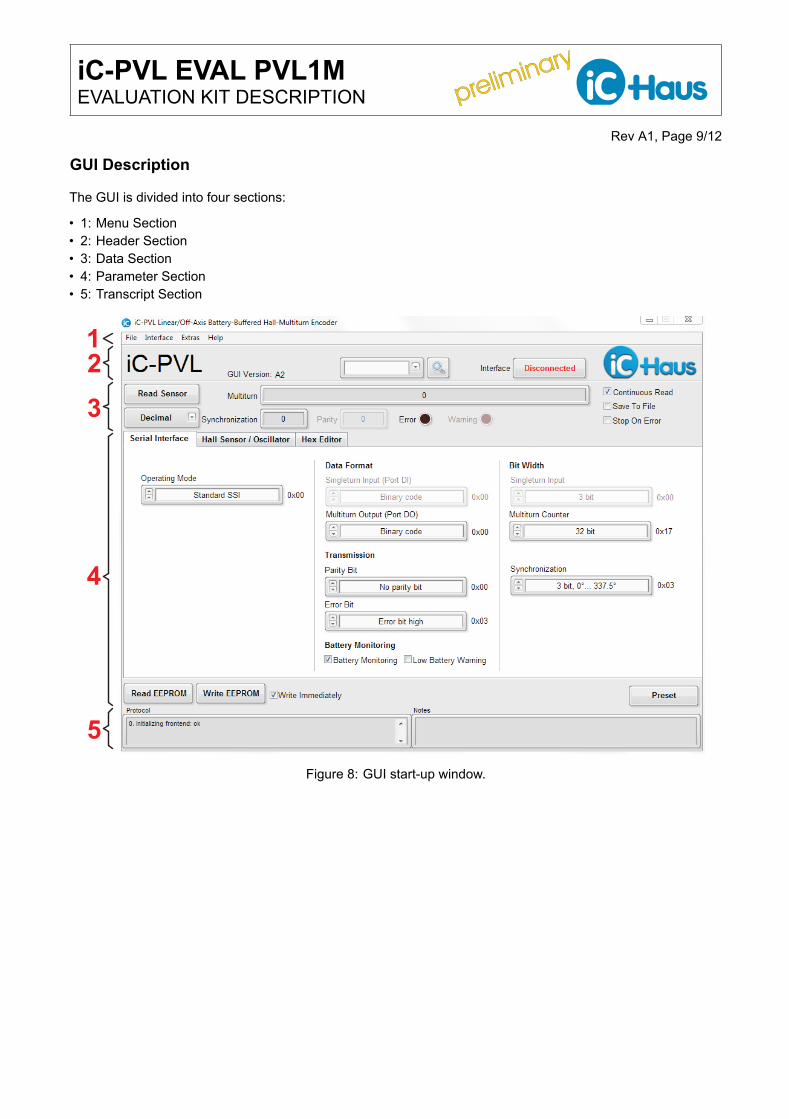
GUI Description
The GUI is divided into four sections:
• 1: Menu Section• 2: Header Section• 3: Data Section• 4: Parameter Section• 5: Transcript Section
12
3
4
5
Figure 8: GUI start-up window.
preliminary
preliminary iC-PVL EVAL PVL1MEVALUATION KIT DESCRIPTION
Rev A1, Page 10/12
Menu Button Description
1 Menu Section
<File> Save Config File Saves the configuration to a file (*.cfg)Load Config File Loads the configuration to the IC (*.cfg)Exit Quits the software
<Interface> No Hardware Disconnects the board and resets the communication betweenPC and adapter.
iC-Interface MB3U Selection for PC-USB adapter MB3U-I2C.Interface Setup Special interface settings.Interface Settings→ Connect & Read Checked: connects the PC adapter and reads the IC registers.
Unchecked: connects the PC adapter without reading the ICregisters.
<Extras> Search Parameter Enables a search field to locate a parameter’s control field. Ifa name match is found, the corresponding control field will behighlighted and focused.
Generate Report Generates a *report.zip archive reporting the current softwarestatus. This report eases debugging software issues by theiC-Haus’ support team.
About GUI release information
2 Header Section Project title, chip version, software version and connection state
3 Data Section Sensor data and status display, read controls.
4 Parameter Section Parameter configuration, read/write access to IC.
<Tabs> Serial Interface Refer to IC datasheet.Hall Sensor / Oscillator Refer to IC datasheet.Hex Editor This tab is a different view of the IC’s register content in HEX
format. Changes made are not automatically updated to the othertabs. Push <Read EEPROM> to update the parameter tabs.
<Parameter> Read EEPROM Reads all parameters from the EEPROM and refreshes the dis-play.
Write EEPROM Writes all parameters from GUI to the EEPROM. A preset isexecuted subsequently to boot up the iC-PVL with the new con-figuration.
Write Immediately If checked, any change to a parameter is transferred to the EEP-ROM immediately. A preset is executed after each parameterchange to boot up the iC-PVL with the new configuration.
Preset Executes a preset command to the iC-PVL to apply parametervalue changes. The iC-PVL boots up and reads the configurationfrom the EEPROM. Designed for Evaluationboard PVL1M. UsesPin 6 on I2C-Plug of the MB3U-I2C USB adapter.

preliminary
preliminary iC-PVL EVAL PVL1MEVALUATION KIT DESCRIPTION
Rev A1, Page 11/12
5 Transcript Section Left: Transcript and feedback messages. Right: Help window.
The GUI software starts with <Interface> Disconnected.When moving the mouse cursor accross an input box, a tooltip comes up and displays the real parameter nameaccording to this box. If a functional parameter description is required, please refer to the IC datasheet.

preliminary
preliminary iC-PVL EVAL PVL1MEVALUATION KIT DESCRIPTION
Rev A1, Page 12/12
REVISION HISTORY
Rel. Rel. Date∗ Chapter Modification PageA1 16-05-25 All Initial release All
iC-Haus expressly reserves the right to change its products and/or specifications. An info letter gives details as to any amendments and additions made to therelevant current specifications on our internet website www.ichaus.com/infoletter; this letter is generated automatically and shall be sent to registered users byemail.Copying – even as an excerpt – is only permitted with iC-Haus’ approval in writing and precise reference to source.iC-Haus does not warrant the accuracy, completeness or timeliness of the specification and does not assume liability for any errors or omissions in thesematerials.The data specified is intended solely for the purpose of product description. No representations or warranties, either express or implied, of merchantability, fitnessfor a particular purpose or of any other nature are made hereunder with respect to information/specification or the products to which information refers and noguarantee with respect to compliance to the intended use is given. In particular, this also applies to the stated possible applications or areas of applications ofthe product.iC-Haus products are not designed for and must not be used in connection with any applications where the failure of such products would reasonably be expectedto result in significant personal injury or death (Safety-Critical Applications) without iC-Haus’ specific written consent. Safety-Critical Applications include, withoutlimitation, life support devices and systems. iC-Haus products are not designed nor intended for use in military or aerospace applications or environments or inautomotive applications unless specifically designated for such use by iC-Haus.iC-Haus conveys no patent, copyright, mask work right or other trade mark right to this product. iC-Haus assumes no liability for any patent and/or other trademark rights of a third party resulting from processing or handling of the product and/or any other use of the product.
∗ Release Date format: YYYY-MM-DD


![Bab 7 Workplace and Family[Print]-PVL](https://static.fdocuments.in/doc/165x107/577cd7ba1a28ab9e789fa2b0/bab-7-workplace-and-familyprint-pvl.jpg)