iAJPY - Defense Technical Information · PDF fileiAJPY c'v Technical Document 1703 September...
26
iAJPY c'v Technical Document 1703 September 1989 Indium Phosphide Planar Gunn Diode M. J. Taylor D. Rubin E. R. Schumacher A. R. Clawson DTIC t ELECTEW-ft Approved for public release; distribution Is unlimited. 90 03 1(t 100;
Transcript of iAJPY - Defense Technical Information · PDF fileiAJPY c'v Technical Document 1703 September...
iAJPY
c'v Technical Document 1703September 1989
Indium Phosphide PlanarGunn Diode
M. J. TaylorD. RubinE. R. SchumacherA. R. Clawson
DTICt ELECTEW-ft
Approved for public release; distribution Is unlimited.
90 03 1(t 100;

NAVAL OCEAN SYSTEMS CENTERSan Diego, California 92152-5000
J. D. FONTANA, CAPT, USN R. M. HILLYERCommander Technical Director
ADMINISTRATIVE INFORMATION
This work was performed for the Office of the Chief of Naval Research, IndependentResearch Programs (IR), Arlington, VA 22217-5000, under program element 0601152N. Thiswork was performed by members of NOSC Codes 561 and 753.
The experiments involving InP Gunn diodes covered by this report were completed inDecember 1987. Due to lack of funds, the results were not published until later.
Released by Under authority ofC. R. Zeisse, Acting Head H. E. Rast, HeadMaterial and Device Electronic MaterialTechnology Branch Sciences Division
ACKNOWLEDGMENTS
The authors gratefully acknowledge the contributions made by the following people:M. E. O'Brien for the SEM work, T. T. Vu for some of the MOCVD epilayer growth, andJ. Crowley and B. Fank of Varian Associates for the VPE epilayer growth.
MA

CONTENTS
IN TRO D U CTIO N ..................................................... 1
BACK G RO U N D ...................................................... 1
EXPERIMENTAL APPROACH ......................................... 3
Epitaxial Layer Growth ........................................... 3D evice Fabrication ...................................... ........ 6
W afer Thinning .............................................. 14
Gold-Plated Beam Lead Formation .............................. 14D ie Separation ............................................... 15
DIO DE TESTIN G ..................................................... 16
SUMMARY AND FUTURE CONSIDERATIONS ........................... 19
Sum m ary .. .. .................................................. 19Future Considerations ............................................ 19
REFERE N CES ....................................................... 21
FIGURES
1. (a) Planar Gunn diode showing current flow parallel to the wafersurface, (b) mesa Gunn diode showing current flow perpendicularto the wafer surface ............................................. 2
2. Steps in planar Gunn diode fabrication: (a) n (active) epilayergrowth, (b) selective etching of n epilayer, (c) selective refilling ofn-layer recesses with n + (contact) epilayer, (d) device isolation ......... 4
3. Examples of Fe-doped InP from different sources, etched 3 minutesin HCI:H3PO 4 1:9: (a) Crysta-Comm material polished in-house byE. R. Schumacher, (b) ICI Americas material polished by ICI, and(c) Sumitomo Electric material polished by Sumitomo. All photos 50x ... 5
4. Examples of first (undoped) epilayer selectively etched to semi-insulating substrate, prior to regrowth: (a) wafer #M0450, 100x,and (b) wafer #M01016, 100x. The epilayer is removed inside therectangles ...................................................... 7
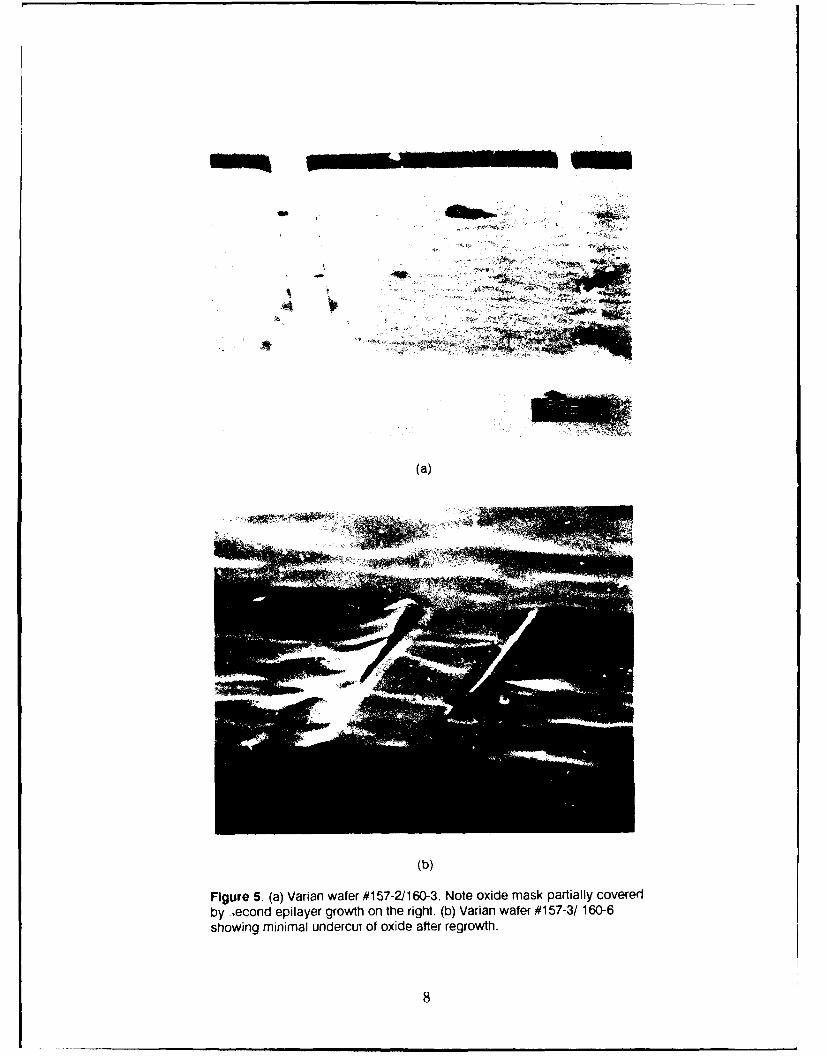
5. (a) Varian wafer #157-2/160-3. Note oxide mask partially coveredby second epilayer growth on the right. (b) Varian wafer #157-3/160-6 showing minimal undercut of oxide after regrowth ............... 8
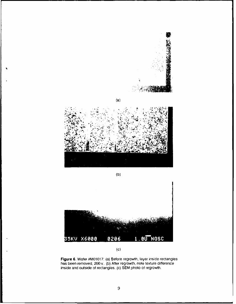
6. Wafer #M01017: (a) Before regrowth, layer inside rectangles hasbeen removed, 200x. (b) After regrowth, note texture differenceinside and outside of rectangles. (c) SEM photo of regrowth ............ 9
7. Resistance versus contact spacing, wafer #M01017/1052 ............... 10
I

FIGURES (continued)
8. Wafer #M01015. Note trench where no regrowth occurred .............. 11
9. (a) Transmission line method (TLM) test pattern. (b) Plot of
information collected using TLM pattern ............................ 12
10. Surface-oriented planar Gunn diode with gold-plated beam leads ........ 15
11. Two examples of finished (beam-leaded) devices ...................... 17
12. RF circuit used for testing beam-leaded InP Gunn diodes .............. 18
TABLES
1. Epilayers and their characterization used for Gunn diode fabrication ..... 13
Accession For J
NTIS IRA&IDTIC TAB ElUjnnnounced [-Ju st i f i osat i on..
By_Distribution/
Amilablllty Codes
-vail ad,/orlDist | Special
ii

INTRODUCTION
Monolithic microwave circuits normally require such extensive processingthat the fabrication of less than several thousand identical circuits is rarely consid-ered. At millimeter-wave frequencies the required precision generally increases andadditional steps, including electron beam lithography (for transistor gate definition)and ion implantation (for contact definition), are often required.
It was our intent to develop indium phosphide (InP) monolithic circuits usingtruly planar Gunn diodes as active devices. Processing would only involve epitaxialgrowth (metalorganic chemical vapor deposition [MOCVD] or vapor phase epitaxy[VPE]), photolithography involving dimensions of 3 gm or more, and the variousprocesses used at lower frequencies. To test the devices in hybrid circuits, gold foilbeam leads would also be fabricated.
At the end of our 2-year program, beam-leaded devices oscillated on hybridcircuits in the 20- to 40-GHz range. Pulsed output power was about 4 mW. Pulsingwas required because heat sinking was not used.
This report covers work completed in December 1987.
BACKGROUND
Although InP is the material of choice for efficient millimeter-wave Gunn-effect diodes, all monolithic oscillators built to date have used GaAs. These deviceshave been fabricated in mesa form, where current flows in a direction perpendicularto the substrate. To bring the lower terminal to the top of the substrate, ion implan-tation is used to create a conductive channel surrounding the mesa. The planar Gunndiode (figure 1), unlike the mesa Gunn diode, has its current flowing parallel to thesurface. Contacts can be made directly to the two ends of the diode. In the early1970s the planar Gunn diode was used in the 10-GHz-frequency range by severalcompanies, including RCA. Similar devices have never been reported to operate atmillimeter-wave frequencies.
Binari, Thompson, and Grubin (1985) of the Naval Research Laboratory havedeveloped an ion-implanted planar InP Gunn diode. However, this diode operatedonly when additional ion implant damage (oxygen implant) was used to define -1 nar-row region near the cathode where the domains are initiated. Another plan.i Gunndevice, developed in Austria, uses a third terminal for control (Hartwig, February1987).
During the initial phase of this project, scanning electron mn1-roscope (SEM)photos indicated that etching the epitaxial material to produce the active Gunnregion generally resulted in sloped walls of 40 degrees or more fhis was true unlessthe diode was oriented along one particular crystallographic direction. The Gunneffect is transit-time dependent, and at 30 GHz, sloped wails could result in as muchas a 25-percent difference in transit times between current traveling along the topand along the bottom of the 0.5- to 1.0-jm-thick device. This difference in geometrywas carefully monitored and utilized during all suV sequent processing.
1

CURRENT FLOW
n+ I n n
(a) PLANAR GUNN DEVICE
CURRENTn+ FLOW
nno+ I
(b) MESA GUNN DEVICE
Figure 1. (a) Planar Gunn diode showing current flow parallel tothe wafer surface, (b) mesa Gunn diode showing current flowperpendicular to the wafer surface.
2

EXPERIMENTAL APPROACH
EPITAXIAL LAYER GROWTH
The surface-oriented planar Gunn diode was fabricated from epitaxial layerssequentially grown as outlined in figure 2. Starting with a piece of semi-insulatingiron-doped InP, an epitaxial layer of nominally undoped InP (carrier concentrationS108 cm-) wqs grown by MOCVD on the polished (100) surface. After selectively
removing portions of the first epitaxial layer, a second epitaxial layer of higher car-rier concentration (n- 1018 cm - 3) was grown in the recesses, creating the structure offigure 2c.
The epitaxial layers used in this program were primarily grown by MOCVD inan in-house reactor, using trimethylindium and phosphine as source materials for theepilayer and silane as the dopant source. Additional layers were provided by VarianAssociates, using a VPE growth system, solid indium and phosphorus trichloride assource materials for the epilayer, and hydrogen sulfide as the dopant source.
The epitaxially grown planar Gunn diode had two unique requirements. First,since the second epilayer was to be grown in selected areas only, a masking layer wasneeded. This layer had to be stable at the InP growth temperatures (- 650 0C), notprovide nucleation sites for InP formation, and be easily removed for subsequentwafer processing. Second, because of the transit-time dependence on geometry asnoted earlier, vertical walls of the recess profile were needed to insure a single transitlength. These two issues were investigated in detail by Taylor and Schumacher(March 1988).
After considerable experimentation, silicon dioxide (SiO2 ) was chosen as themasking layer for selectively etching the first epilayer and regrowing the secondlayer. The chemical etchant used to produce vertical sidewalls in the first epilayerwas HCI:H 3PO4 1:9. This resulted in vertical walls parallel to the (011) direction andsloped walls parallel to the (011) direction. Most diode structures were oriented sothe transit path of the current would be in the (01 i) direction (vertical interfacebetween n and n+ regions). For comparison, some diodes were oriented 90 degreesfrom this (with the n/n+ interface a sloped profile).
The epilayer growth/regrowth process encountered several unexpected prob-lems. Not only was the wall profile of the interface dependent on crystal orientation(easily addressed by device orientation), but the bulk InP on which the epilayers weregrown came from different suppliers, and materials from each supplier etched quitedifferently. Representative photos of etch tests are shown in figure 3. Some of the dif-ferences in surface features can be attributed to the following: (a) quality of thestarting crystal, i.e., purity of the material, degree of contamination, number of inclu-sions, etc., (b) surface finish and degree of subsurface damage still remaining. Mate-rial quality is a continuing concern for InP users. Suppliers are constantly seeking toimprove the bulk quality and surface finish of InP wafers. Each year improvementsare made in these areas.
Substrate surface treatment also had a significant effect on the surfacemorphology of the subsequent epilayer. Unavoidable surface treatment included
3

n
InP
(a)
InP
(b)
n + nfl
InP
(d)
Figure 2. Steps in planar Gunn diode fabrication:(a) n (active) epilayer growth, (b) selective etching of n epilayer,(c) selective refilling of n-ayer recesses with n+ (contact) epilayer,and (d) device isolation.

(a)
(b)
(c)
Figure 3. Examples of Fe-doped InP from different sources, etched 3minutes in HCI:H 3PO 4 1:9: (a) Crysta-Comm material polished in-houseby E. R. Schumac.her, (b) IC Americas material polished by ICI, and(c) Sumitomo Electric material polished by Sumitomo. All photos 50X.
5

precleaning prior to introduction into the grrowth roactor, selective etching for pat-tern definition, and ambient conditions once in the growth chamber. Common surfacetreatment techniques, thought to be standard for other processing, were often foundto be too harsh for this device process. Handling and cleaning procedures unique tothis device were developed. Such improved techniques have recently found applicationin new and novel devices currently being fabricated in NOSC's Material and DeviceTechnology Branch (Code 561).
The selective etching process uncovered two potential stumbling blocks. Whenthe first epilayer is selectively removed (exposing the underlying semi-insulating sub-strate), the exposed surface should be smooth and relatively free of defects for it is onthis surface that the second epilayer regrowth will take place. Figure 4 shows exam-ples of a good wafer and a poorly etched wafer. The second epitaxial layer can beexpected to nucleate and grow much more nonuniformly in the latter case.
The other stumbling block occurred when masked wafers were sent to VarianAssociates for regrowth. Standard procedure was to saturate the indium source withphosphorus trichloride prior to epilayer formation. It was during this time that thepattern was severely etched (figure 5a), resulting in an undercutting of the SiO 2masking layer to such an extent that no active InP layer remained. As seen in theright-hand side of the photo, the second epilayer was able to grow and actually burythe unsupported oxide "mask" within it. Taking this into account, Varian Associateswas able to alter its VPE process, and subsequently provided NOSC with the layershown in figure 5b.
The most severe problem occurred when the in-house MOCVD reactor becamecontaminated due to failure of the hydrogen purifier to produce dry H2 . Before theproblem was discovered, several epilayers were processed for diode use. Figure 6 is anexample of growth during this time. Figure 7, a resistance plot of this wafer(M01017/M01052), illustrates the nonuniformity of the layer, not only in surface mor-phology, but in electrical characteristics as well. (The more uniform the epilayers are,the smaller the spread in resistance measurements.) Figure 8 shows a second growthdifficulty. In a few instances, the regrowth epilayer failed to completely fill in therecess area, resulting in a discontinuity between the n+ contact region and the nactive region. The reason for the noncontinuous epilayer growth is not known at thistime, although wet H2 is again suspected.
DEVICE FABRICATION
After the second and final epilayer growth, the SiO 2 masking layer wasstripped and the contact resistance of the Gunn device was determined using alloyedgold/germanium contact metal and the transmission line method (TLM) (Look, 1987)of measuring resistance, outlined in figure 9. The objective was to distinguish thosestructures with low contact resistance (Rc), necessary to permit Gunn oscillation,from others showing too high a resistance. (High contact resistance was also encoun-tered by Varian Associates when they pursued similar work [C. owley, 19841.) Thereare a number of factors contributing to the resistance value, such as quality of then/n+ interface, the carrier concentration of the epilayers, overall layer thickness, andthe contact metal/semiconductor interface. Table 1 summarizes the results of theepilayers used on this project.
6

(a)
*i
(b)
Figure 4. Examples of first (undoped) epilayer selectively etched tosemi-insulating substrate, prior to regrowth: (a) wafer #M0450, x00 x,and (b) wafer #M01016, 1Ox. The epilayer is removed inside therectangles.
7
- -
(a)
(b)
Figure 5. (a) Varian wafer #157-21160-3. Note oxide mask partially coveredby ,econd epilayer growth on the right. (b) Varian wafer #157-3/ 160-6showing minimal undercui of oxide after regrowth.
8
(a)
F4 .'=2
(b)
(c)
Figure 6. Wafer #M01017: (a) Before regrowth, layer inside rectangleshas been removed, 200x. (b) After regrowth, note texture differenceinside and outside of rectangles. (c) SEM photo of regrowth.
9

1000
900
800
700
600
50
z x3 00
xx
400
300030405
1000

Figure 8. Wafer #M01015. Note trench where no regrowth occurred.

I d t.- d [1- 4 - d - 13 -- d
R, Rc + c Ic R R
w C
0z
R,,
(2Rc)
0 SPACING
(b)
Figure 9. (a) Transmission line method (TLM) test pattern.(b) Plot of information collected using TLM pattern.
12

M 00 to It t- CIO
t-~~ cq Lf0 cc -0 -"5't enCDC0 u oL O na .C
M ) C ,5 TT0 -c000 0 m0 tC m-)c ' 4c 4C o c
m M; V
Lr to 0Crco 000
COC/
UD LO V) t- E- Onr7nO(
v V~ Lo UD-M M-- - - vIt t - t oL
.0 (m 000 00 0 0 9 000 ot'0C C 00 C.Ou)t C p-C Uq )t
C.) 4 qC 4 qM M M
Lf13

The most promising devices (as noted in table 1) were then selected for furtherprocessing. This included wafer thinning, gold-plated beam lead formation, and sepa-ration of the individual diodes. These topics will be addressed in the following sec-tions.
Wafer Thinning
It was necessary to thin the substrates from 0.020 inch to 0.004 inch to allowfor possible heat sinking. The diode fabrication process required that further photo-lithography be performed after substrate thinning. Hence, the wafers needed to berelatively flat and uniform (suitable for use in a mask aligner) after thinning. Chemi-cal thinning agents were experimented with, but none gave a suitably smooth and flatfinished surface. It was, therefore, necessary to chemo-mechanically thin and polishthe substrates versus thinning by chemical etching alone.
The nature of the thinning process used required that the blocking side of thewafers be relatively flat. Therefore, wafer thinning and polishing on the backsidewere accomplished prior to beam lead formation on the frontside. Because of theexpense of thinning wafers and their extreme fragility afterwards, all preliminarygold-plating and etching work was done on bulk InP that was 0.020 inch thick.
Gold-Plated Beam Lead Formation
For the diodes to be tested at millimeter-wave frequencies, they had to beattached to hybrid circuits. Wirebonding was ruled out because of the inductanceassociated with the wire loops. Flat soldered leads were used instead.
The first diodes were attached with gold ribbon leads. Due to the small size ofthe chip and the active diode region (300 by 250 gm and 3 to 4 gm respectively),hand-soldering the lead to the chip, without damaging the device, was very difficult.Leads were successfully attached to a small group of devices, which were then sol-dered into the test circuitry. The yield was low and only one device from this firstgroup showed signs of oscillation.
Gold-plated beam leads (see figure 10), produced by photolithography on thewhole wafer, were preferred. Not only were the device and lead dimensions more suit-able for lithography, but dozens of firmly attached identical leads could be producedat one time. The desire to goldplate onto patterned semiconductor material led to theexploration of several alternative approaches.
Both selective plating and blanket plating followed by selective etching wereinvestigated. Although selective plating appeared simpler, there were two drawbacks.First, the masking resist was not designed for use in such a harsh environment (goldcyanide, heated to 700C). The resist film reticulated when left in solution forextended periods. Second, not only did the plated gold film mushroom over the top ofthe resist as anticipated, but the weakened resist film permitted some plating tooccur beneath it as well, shorting devices by bridging the contact pads together.Selective etching produced more satisfactory results, despite its drawbacks of poorlithographic image due to the graininess of the plated gold film and difficulty inrealigning to features beneath a thick-plated film.
To circumvent the above mentioned problems, different masking layers weretried. Dupont Pyralin P12570 polyimide, noted for its good adhesion and chemical
14

GOLD-PLATED BEAM LEADS
SEMI-INSULATING InP
Figure 10. Surface-oriented planar Gunn diode with gold-plated beam leads.
resistance, was not suitable due to the difficulty in removing it for rework and itsshort shelf life. AZ 4330 photoresist, while providing thick transparent films suitablefor plating, did not exhibit adequate chemical resistance. Shipley 1450J photoresist,spun at 4000 r/min, was very easy to process and reasonably resistant to the platingand etching solutions.
Two noteworthy phenomena were observed while goldplating the thinnedwafers. Using thick (0.020 inch) wafers, gold was electroplated only in the exposedconductive regions of the front surface. Using thin (0.004 inch) wafers, goldplatingalso occurred on the sides and back surface of the semi-insulating InP. It is interest-ing to note that the gold deposits on the back often originated in the thinning sleeksand then spread across the wafer. Also, a faint image of the plated front surface pat-tern was apparent on the back surface of the thinned wafers. Neither of these phe-nomena occurred on the thicker wafers.
Die Separation
Originally, the finished diodes were to be individually separated by selectivelyetching through the substrate from the backside of the wafer. Although many wetetchants were investigated, from concentrated hydrochloric acid to various concentra-tions of bromine/methanol, they all exhibited severe undercutting of the etch mask.Ferric chloride, a known photochemical etchant for InP (Lubzens, March 1977), wasfound to be ineffective on semi-insulating material.
Because no suitable chemical etchant was found, the individual beam-leadeddiodes were manually diced out. Due to their small size (300 by 250 gm), they were
15

diced individually under a microscope. At this time, differences in hardness (orbrittleness) of the starting bulk material became evident. Some substrates cleavedreadily along the desired lines, while others fractured with difficulty and often not atright angles. Figure 11 gives two examples of the finished diodes.
In some instances, the gold-plating on the backside of the wafer remainedintact. It was to be utilized for alternative heat-sinking later in the testing. Theplated gold film, however, contributed to the difficulty of die separation since it didnot necessarily fracture along the same lines as the InP substrate. Those diodes thatremained intact at this point were ready for diode testing.
DIODE TESTING
Figure 12 shows the 0.5- by 0.5-inch circuit used for diode testing. The dielec-tric used was 0.005-inch Rodgers 6010.5 (dielectric constant = 10.5). The upper cop-per surface was pre-etched to about 0.004 inch to allow 1-mil definition (with littleundercutting). Due to the dc block/transformer, a 50-ohm load at the coaxial outputshould transform to about 5 ohms at the diode. The tuning stub, somewhat longerthan 1/4 wavelength, should behave as an inductive reactance at the oscillation fre-quency, offsetting the diode capacitance. To oscillate, the diode's negative resistancemust adjust itself to equal the total circuit positive resistance and the total seriesreactance must equal zero. In actuality, this happens when the RF voltage swingacross the active part of the device changes on both sides of the dc bias point to com-pensate for the circuit.
Since no heat sink was used for the beam-leaded diodes, the dc power waspulsed, generally less than 0.5 gs. Dozens of diodes from eight different runs weretested. The one run which provided many active devices was from an undopedepilayer grown by Varian Associates with the n+ contact epilayer regrown in therecesses using NOSC's MOCVD reactor. The diodes showing oscillation were fabri-cated with sloped n/n+ interfaces. The companion wafer (the same epilayer runs butwith vertical n/n+ interfaces) did not survive to the beam lead stage. This was unfor-tunate since the resistance measurements looked promising and a direct comparisonof geometry was desired.
Results on the one good wafer included pulsed power in the 4-mW range andoscillation frequencies in the 20- to 40-GHz region. Attempts at heat-sinking, bybonding the diode to the fixture surface through a hole in the substrate with conduc-tive epoxy, were unsuccessful.
16

Figure 11. Two examples of finished (beam-leaded) devices.
17

1 : 1 j ~~DC INPUTJ
ISLN
DC BLOCK/XFMR DIODE- I TUNING STUB
K CONNECTORC O A X I A L O U T P U T G RN D
Figure 12. RF circuit used for testing beam-leaded InP Gunn diodes.
18

SUMMARY AND FUTURE CONSIDERATIONS
SUMMARY
A Gunn diode that exhibited oscillations within the 20- to 40-GHz-frequencyrange was successfully fabricated using epitaxially grown layers. The concept of selec-tively removing portions of one epilayer and then refilling the recesses with a secondepilayer was demonstrated. The working structure showed low resistance across then/n+ interface, as expected.
All of the processing techniques developed for the InP Gunn diode work havebeen incorporated into current work in Code 561. The vertical sidewall etching isbeing used to fabricate self-aligned junction field-effect transistors (JFETs). Regrowthin selected recesses is being utilized to fabricate p-i-n photodiodes as part of an InPintegrated circuit. Thinned InP wafers are used when testing microwave devices suchas power FETs, amplifiers, and photoconductive switches. Plated beam leads are usedto attach discrete switches to test circuitry.
In addition, the successful Gunn diodes fabricated and tested during this pro-ject have renewed Varian Associates' interest in surface-oriented planar Gunn diodes.NOSC is currently collaborating with Varian Associates in this effort. Epilayers arebeing provided by Varian Associates, and device-fabrication and testing are beingdone at NOSC.
FUTURE CONSIDERATIONS
Areas of further interest stimulated by this project include the following fourtopics. First, the effect of backside thinning on frontside device performance shouldbe investigated. Several interesting effects became evident when the plating processon thin wafers was compared with the process on thick wafers. The thin wafersplated as though they were conducting, instead of semi-insulating, substrates. Also,images of front surface features appeared on the back surface of the thinned wafersduring plating. Neither of these two effects were seen when plating the thickerwafers.
Second, the technique of recessed regrowth in selective areas is extremely use-ful when fabricating planar (versus mesa) integrated circuits. But more work isneeded in this area. The Gunn diode yield was much less than 100 percent and morework is required to improve this yield. Increased understanding is needed in the areasof growth nucleation (or lack of it), effects of surface preparation, and effect of crystalorientation on regrowth.
Third, the vertical etch process may have introduced crystal surfaces thatwere not only resistant to etching but resistant to regrowth nucleation as well. This,in turn, may have contributed to the low yield of suitable epilayers for this work. Amore thorough study is needed to determine why certain epilayers failed to support aregrowth layer.
19

Finally, a topic of special interest is the task of separating individual devicesfrom the process wafer by backside etching, as opposed to scribing or dicing.Attempts were made at wet-chemical etching but the etchants investigated wereeither ineffective on semi-insulating material or undercut so severely that the mask-ing layer was completely removed. For technology transfer, an automated (versus thelabor-intensive manual dicing) procedure is necessary.
20
REFERENCES
1. Binari, S. C., P. E. Thompson, and H. L. Grubin. January 1985. "Self-AlignedNotched Planar InP Transferred-Electron Oscillators," IEEE Electron Device Let-ters, vol. EDL-6, no. 1, pp. 22-24.
2. Hartwig, Thim. 28 February 1987. "A Planar IC-Compatible Transferred Elec-tron Device for Millimeter-Wave Operation," 2nd Periodic Report for ContractNo. DAJA 45-86-C-0039.
3. Taylor, M. J. and E. R. Schumacher. March 1988. "Vertical Side-Wall Etching ofIndium Phosphide," Naval Ocean Systems Center Technical Note 1521.1
4. Look, D. C. April 1987. "Mobility Measurements with a Standard Contact Resis-tance Pattern," IEEE Electron Device Letters, vol. EDL-8, no. 4, pp. 162-164.
5. Crowley, J. D. December 1984. "Monolithic InP Circuit Development," NavalOcean Systems Center Contractor Report 256.
6. Lubzens, D. 31 March 1977. "Photoetching of InP Mesas for Production of mm-Wave Transferred-Electron Devices," Electronic Letters, vol. 13, no. 7, pp.171-172.
1 NOSC Technical Notes (TNs) are working documents and do not represent an official policy statement of the
Naval Ocean Systems Center. For further information, contact the author.
21

REPORT DOCUMENTATION PAGE FNo.App,4ve8Public reporting burden for this collection of information is estimated to average 1 hour per response, Including the time for reviewing ins1ructions searching exisling data sources, gathering and•ialntaring the data needed, and completing and reviewing the oiteclion of information SeO comments regarding this burden estimate or any ofther aspect of this collection of Information Including.uggestlons for reducing this burdenr, to Washlngton Headquarters Services, Directorate fo Information Operations and Reports 1215 Jefferson Davis Highway. Suite 1204. Arlington. VA 22202-4302and to the Office of Management and Budgei Paperworr Reduction Project (0704-0188). Washington. DC 20603
1 AGENCY USE ONLY (Leave bAOl 2 REPORT DATE 3 REPORT TYPE AND DATES COVERED
September 1989 Final: Dec 85 - Dec 87
4 TITLE AND SUBTITLE 5 FUNDING NUMBERS
INDIUM PHOSPHIDE PLANAR GUNN DIODE PE: 0601152NPROJ: 75-ZT46
6 AUTHOR(S) SUBPROJ: RR0001
M. J. Taylor, D. Rubin, E. R. Schumacher, A. R. Clawson ACN: DN306 217
7 PERFORMING ORGANIZATION NAME(S) AND ADORESS(ES) 8 PERFORMING ORGANIZATIONPEPORT NUMBER
Naval Ocean Systems CenterSan Diego, CA 92152-5000 NOSC TD 1703
9 SPONSORING/MONITORING AGENCY NAME(S) AND ADORESS(ES) 10 SPONSORiNG/MONITORINGAGENCY REPORT NUMBER
Office of the Chief of Naval ResearchIndependent Research Programs (IR)Arlington, VA 22217-5000
11 SUPPLEMENTARY NOTES
12a DISTRIBUTION/AVAILABiULY STATEMENT 12b. DISTRIBUTION COO
Approved for public release; distribution is unlimited.
13 ABSTACT (MAamthu 20 w rds)
•--An indium phosphide (InP) planar Gunn diode showing oscillations in the 20- to 40-GHz-frequency range wassuccessfully fabricated and Lested using epitaxially grown layers. Also demonstrated was the concept of selectively removingportions of one epilayer and refilling the recesses with a second epilayer. The working structure showed low resistance acrossthen /r+ interface.
Processing techniques developed during the InP planar Gunn diode work are now incorporated into current workat NOSC. Also, successes in these experiments resulted in renewed interests in surface-oriented planar Gunn diodes.
//
/
14 SUBJECT TERMS 15 NUMBER OF PAGES
28indium phosphide (InP), vapor phase epitaxy (VPE), planar Gunn diode, metalorganic chemical vapor is PRICE COoEdeposition (MOCVD), monolithic circuits, epildyer growth, substrates,
17 SECURrTY CLASSIFICATION 18 SECURITY CLASSIFICATION 19 SECURrrY CLASSIFICATION 20 UMITATION OF ABSTRACTOF REPORT OF THIS PAGE OF ABSTRACT" \
UNCLASSIFIED UNCLASSIFIED UNCLASSIFIED UNLIMITED
NSN 7540-01-280-5500 Standard form 298