I P S T Semicond. Sci. Technol. 19 The effect of ultra ... · CE: AK INSTITUTE OF PHYSICS...
5
CE: AK INSTITUTE OF PHYSICS PUBLISHING SEMICONDUCTOR SCIENCE AND TECHNOLOGY Semicond. Sci. Technol. 19 (2004) 1–4 PII: S0268-1242(04)75986-6 The effect of ultra-thin Al 2 O 3 layers on the dielectric properties of LaAlO 3 thin film on silicon L Yan 1 , L B Kong 2 and C K Ong 3 1 Center for Superconducting and Magnetic Materials (CSMM), National University of Singapore, Lower Kent Ridge Crescent, 119260, Singapore 2 Temasek Laboratories, National University of Singapore, 10 Kent Ridge Crescent, 119260, Singapore 3 Center for Superconducting and Magnetic Materials (CSMM), National University of Singapore, Lower Kent Ridge Crescent, 119260, Singapore E-mail: [email protected] Received 12 February 2004 Published DD MMM 2004 Online at stacks.iop.org/SST/19/1 DOI: 10.1088/0268-1242/19/0/000 Abstract HHigh-k LaAlO 3 (LAO) thin films with and without Al 2 O 3 buffer layers were deposited on n-type silicon substrates using a pulsed laser deposition method. The dielectric constant of the LAO thin film increased from 5.2 to 23.1 as its thickness increased from 20 to 500 ˚ A. The effective dielectric constants of the LAO (120 ˚ A)/Si and LAO(105 ˚ A)/Al 2 O 3 (15 ˚ A)/Si were 12.5 and 23.2, respectively. The flatband voltage of the LAO(105 ˚ A)/ Al 2 O 3 (15 ˚ A)/Si sample decreased from 2.0 V to 1.2 V after the sample was annealed for 5 min at 850 ◦ C in air atmosphere, while the dielectric constant value of the annealed sample did not changed. It was found that a 15 ˚ A thick Al 2 O 3 buffer layer could enhance the dielectric properties of the LAO thin film, making it one of the good candidates for high-k materials. 1. Introduction LaAlO 3 (LAO) crystal has an ideal cubic perovskite ( O 1 h ) structure at high temperature, which transforms into a rhombohedral (D 2d − R3c) form at a temperature below 800 K [1]. LAO single crystal has a dielectric constant of 24–25, a large bandgap of 5 eV, and good thermal stability up to 2100 ◦ C [2]. It is considered as one of the best oxide materials to be used in the sub-0.1 µm metal-oxide-semiconductor (MOS) field effect transistor (FET) devices. Some research works on LAO thin films deposited on silicon substrate have been published in recent years. Park et al [3] reported amorphous LAO thin films with a dielectric constant of 20–25 deposited on silicon substrate by molecular beam deposition. They found that the dielectric constant of the amorphous LAO thin films decreased greatly after high temperature annealing. Amorphous LAO thin film deposited by laser molecular beam epitaxy (LMBE) on silicon with clean interface having a dielectric constant of 14 was also reported by Yan et al [4]. Xiang et al reported the chemical composition and dielectric characteristics of LAO thin film at different deposition oxygen partial pressures [5]. Crystal LAO thin films with (00l) orientation have also been successfully grown on silicon by atomic layer epitaxy (ALE) process [6], whose dielectric properties have not been reported. Generally, the dielectric constant of LAO thin film (< 120 ˚ A) deposited on silicon by pulsed laser deposition (PLD) is only 5–12, which is much lower than that of LAO ceramics [2]. The low dielectric constant value of LAO thin film can be mainly attributed to the poor interfacial characteristics between LAO and Si substrate. To address this problem, we introduced a thin Al 2 O 3 (AO) layer at the interface between LAO and Si substrate. This paper compares the dielectric and electrical properties of the LAO thin films on silicon substrates with and without a thin layer of AO. 2. Experimental details The LAO and AO thin films were deposited on the n-type silicon substrate (adopting concentration of 10 17 cm −3 ) by PLD system with a background vacuum of 2 × 10 −7 mbar 0268-1242/04/000001+04$30.00 © 2004 IOP Publishing Ltd Printed in the UK 1
Transcript of I P S T Semicond. Sci. Technol. 19 The effect of ultra ... · CE: AK INSTITUTE OF PHYSICS...

CE: AK
INSTITUTE OF PHYSICS PUBLISHING SEMICONDUCTOR SCIENCE AND TECHNOLOGY
Semicond. Sci. Technol. 19 (2004) 1–4 PII: S0268-1242(04)75986-6
The effect of ultra-thin Al2O3 layers onthe dielectric properties of LaAlO3 thinfilm on siliconL Yan1, L B Kong2 and C K Ong3
1 Center for Superconducting and Magnetic Materials (CSMM), National University ofSingapore, Lower Kent Ridge Crescent, 119260, Singapore2 Temasek Laboratories, National University of Singapore, 10 Kent Ridge Crescent,119260, Singapore3 Center for Superconducting and Magnetic Materials (CSMM), National University ofSingapore, Lower Kent Ridge Crescent, 119260, Singapore
E-mail: [email protected]
Received 12 February 2004Published DD MMM 2004Online at stacks.iop.org/SST/19/1DOI: 10.1088/0268-1242/19/0/000
AbstractHHigh-k LaAlO3 (LAO) thin films with and without Al2O3 buffer layerswere deposited on n-type silicon substrates using a pulsed laser depositionmethod. The dielectric constant of the LAO thin film increased from 5.2 to23.1 as its thickness increased from 20 to 500 A. The effective dielectricconstants of the LAO (120 A)/Si and LAO(105 A)/Al2O3(15 A)/Si were12.5 and 23.2, respectively. The flatband voltage of the LAO(105 A)/Al2O3(15 A)/Si sample decreased from 2.0 V to 1.2 V after the sample wasannealed for 5 min at 850 ◦C in air atmosphere, while the dielectric constantvalue of the annealed sample did not changed. It was found that a 15 A thickAl2O3 buffer layer could enhance the dielectric properties of the LAO thinfilm, making it one of the good candidates for high-k materials.
1. Introduction
LaAlO3 (LAO) crystal has an ideal cubic perovskite(O1
h
)
structure at high temperature, which transforms into arhombohedral (D2d −R3c) form at a temperature below 800 K[1]. LAO single crystal has a dielectric constant of 24–25, alarge bandgap of 5 eV, and good thermal stability up to 2100 ◦C[2]. It is considered as one of the best oxide materials to be usedin the sub-0.1 µm metal-oxide-semiconductor (MOS) fieldeffect transistor (FET) devices. Some research works on LAOthin films deposited on silicon substrate have been publishedin recent years. Park et al [3] reported amorphous LAO thinfilms with a dielectric constant of 20–25 deposited on siliconsubstrate by molecular beam deposition. They found that thedielectric constant of the amorphous LAO thin films decreasedgreatly after high temperature annealing. Amorphous LAOthin film deposited by laser molecular beam epitaxy (LMBE)on silicon with clean interface having a dielectric constant of14 was also reported by Yan et al [4]. Xiang et al reported thechemical composition and dielectric characteristics of LAO
thin film at different deposition oxygen partial pressures [5].Crystal LAO thin films with (00l) orientation have also beensuccessfully grown on silicon by atomic layer epitaxy (ALE)process [6], whose dielectric properties have not been reported.
Generally, the dielectric constant of LAO thin film(<120 A) deposited on silicon by pulsed laser deposition (PLD)is only 5–12, which is much lower than that of LAO ceramics[2]. The low dielectric constant value of LAO thin film can bemainly attributed to the poor interfacial characteristics betweenLAO and Si substrate. To address this problem, we introduceda thin Al2O3 (AO) layer at the interface between LAO and Sisubstrate. This paper compares the dielectric and electricalproperties of the LAO thin films on silicon substrates with andwithout a thin layer of AO.
2. Experimental details
The LAO and AO thin films were deposited on the n-typesilicon substrate (adopting concentration of 1017 cm−3) byPLD system with a background vacuum of 2 × 10⁻⁷ mbar
0268-1242/04/000001+04$30.00 © 2004 IOP Publishing Ltd Printed in the UK 1

L Yan et al
with a KrF excimer laser (LAMBDA PHYSIK, wavelengthand pulse duration are 248 nm and 30, respectively). LAOQ1
target with a composition of La:Al: O = 1: 1: 3 was madevia the conventional ceramic processing. LaAlO3 structurewas well formed in the target, evidenced by x-ray diffraction(XRD) measurement. The target of Al2O3 is a conventional99.9% Al2O3 ceramic plate. The n-type silicon substrate wasfirst ultrasonically cleaned in pure alcohol and pure acetonefor about 10 min each, and then dipped into 5% HF dilutedsolution for 10–20 s to remove the natural silicon oxides andform a H-terminated surface. The deposition was conductedwith the following parameters: the distance between targetand substrate was 50 mm, the laser energy density focused onthe target was about 1.5 J cm−2 at a frequency of 2 Hz, thedeposition temperature was 600 ◦C and the oxygen pressurewas 0.25 mbar. Two groups of LAO thin films with thicknesses20 to 250 A were deposited, one of which was buffered witha thin layer Al2O3 (15 A). Some of the samples were ex situannealed at 850 ◦C for 8 min at air atmosphere.
The crystalline property of the LAO samples wascharacterized by an XRD measurement and their surfacemorphology was examined by an atomic force microscopy(AFM). For electrical characterization, MOS capacitors witha structure of Au/LAO/AO/Si/Au or Au/LAO/Si/Au werefabricated using Au gate electrodes with an area of 3.14 ×10⁻⁴ cm2, deposited using a magnetic sputtering equipment.The characteristics of the capacitance versus voltage (C–V )at 1 MHz measurement frequency and capacitance versusfrequency ranging from 85 kHz to 5 MHz were recordedusing an HP4192ALCR meter. The leakage current densityversus voltage (J–V ) was measured by a Radiant TechnologyRT6000S ferroelectric tester. The equivalent oxide thickness(EOT) was extracted from the accumulation capacitance. Allthe measurements were carried out at room temperature.
3. Results and discussion
All the LAO thin films on silicon substrates with and withoutthe AO buffer layer are in the amorphous state, evidenced bythe XRD measurement. Even the annealed LAO thin films arealso amorphous. This is consistent with the finding of Saderet al [7] and Molodyk et al [8], where the amorphous LAOfilms deposited at low temperatures did not crystallize afterhigh temperature annealing.
AFM examinations demonstrated that no particles andsharp islands were found for all samples. The root-mean-square (RMS) surface roughness of the LAO samples withoutand with the AO buffer layer in an area of 2 × 2 µm2 wasabout 4 and 6 A respectively, indicating that the surface of theLAO thin films deposited on silicon is atomic-scale smooth.Figure 1 shows the two-dimensional (a) and three-dimensional(b) AFM image of as-deposited 105 A LAO thin film on Siwith 15 A AO buffer layer. The RMS of the film within an areaof 2 × 2 µm is 4.5 A. It should be noted that the roughnessof the LAO thin films remained almost unchanged even afterpost-annealing at 850 ◦C for 8 min.
The C–V curves of the LAO thin film with thickness of20, 50, 120 and 500 A directly deposited on silicon are shownin figure 2. The inset shows the effective dielectric constantof the LAO thin films versus their thickness. The dielectric
Figure 1. Two-dimensional (a) and three-dimensional (b) AFMimages of the 105 A LAO thin film on Si with a 15 A AO bufferlayer.
(This figure is in colour only in the electronic version)
-3 -2 -1 0 1 2 3
0
150
300
450
600
750
0 100 200 300 400 500
5
10
15
20
25
500 Å
120 Å
50 Å
Cap
acita
nce
(pF
)
Bias Voltage (V)
20 Å
Die
lect
ric c
onst
ant
LAO thickness (Å)
Figure 2. C–V properties of the LAO thin films directly depositedon Si substrates with thicknesses of 20, 50, 120 and 500 A, whichwere measured at the test frequency 1 MHz at room temperature.The inset image is the dielectric constant of LAO thin film depositeddirectly on Si by PLD as a function of its thickness.
constants of the LAO thin films with the thicknesses of 20, 50,120 and 500 A were 5.2, 9.4, 12.5 and 23.1, respectively. Thedielectric constant of the LAO thin films directly depositedon Si increased with the increase of its thickness. As the
2
The effect of ultra-thin Al2O3 layers on the dielectric properties of LaAlO3 thin film on silicon
-6 -4 -2 0 2 4 6
0
100
200
300
400
500
600
as-deposited
LAO(105Å)/AO(15Å)/Si
Cap
acita
nce
(pF
)C
apac
itanc
e (p
F)
Voltage (V)
ex situ Annealing
(a)
(b)
0 1000 2000 3000 4000 50000
20
40
60
80
100
Frequency (kHz)
LAO(105 Å)/AO(15 Å)/Si
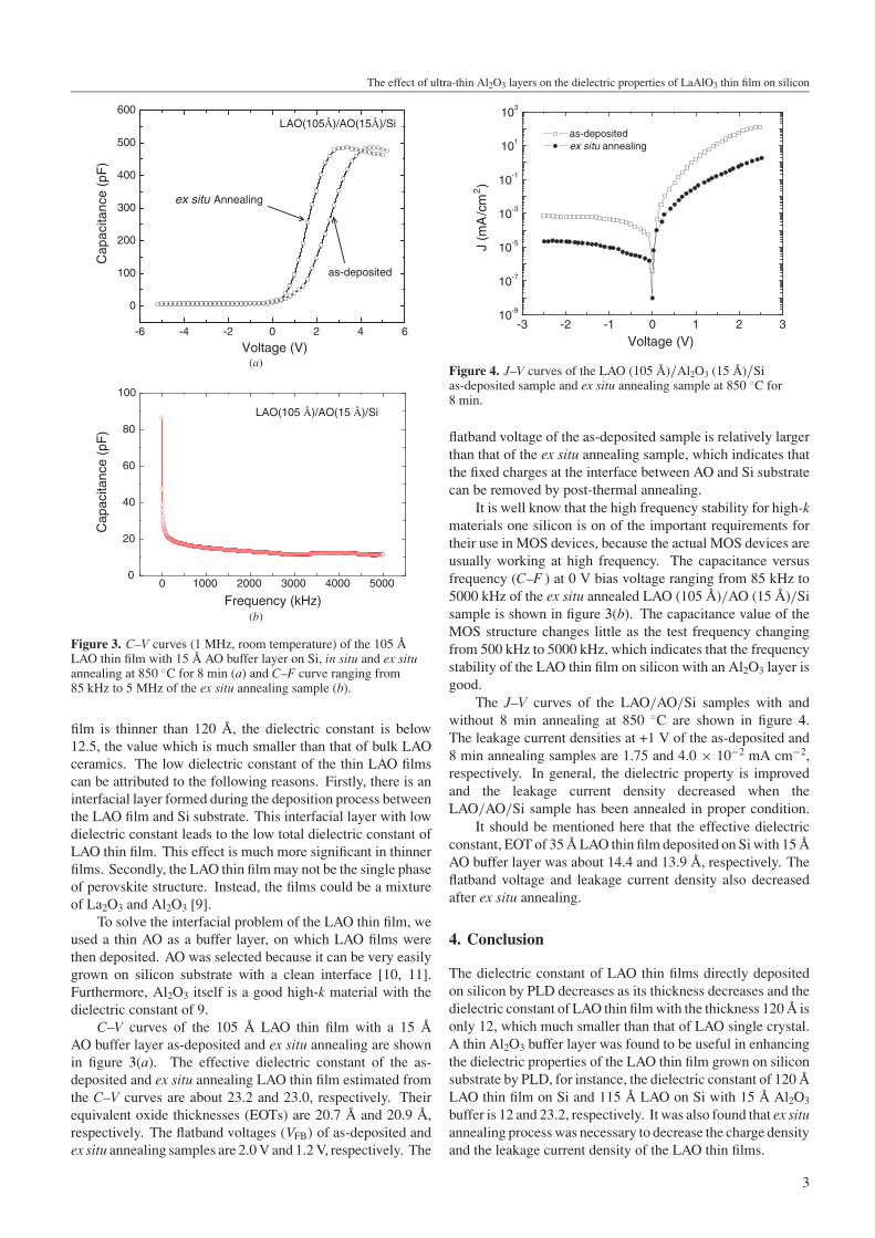
Figure 3. C–V curves (1 MHz, room temperature) of the 105 ALAO thin film with 15 A AO buffer layer on Si, in situ and ex situannealing at 850 ◦C for 8 min (a) and C–F curve ranging from85 kHz to 5 MHz of the ex situ annealing sample (b).
film is thinner than 120 A, the dielectric constant is below12.5, the value which is much smaller than that of bulk LAOceramics. The low dielectric constant of the thin LAO filmscan be attributed to the following reasons. Firstly, there is aninterfacial layer formed during the deposition process betweenthe LAO film and Si substrate. This interfacial layer with lowdielectric constant leads to the low total dielectric constant ofLAO thin film. This effect is much more significant in thinnerfilms. Secondly, the LAO thin film may not be the single phaseof perovskite structure. Instead, the films could be a mixtureof La2O3 and Al2O3 [9].
To solve the interfacial problem of the LAO thin film, weused a thin AO as a buffer layer, on which LAO films werethen deposited. AO was selected because it can be very easilygrown on silicon substrate with a clean interface [10, 11].Furthermore, Al2O3 itself is a good high-k material with thedielectric constant of 9.
C–V curves of the 105 A LAO thin film with a 15 AAO buffer layer as-deposited and ex situ annealing are shownin figure 3(a). The effective dielectric constant of the as-deposited and ex situ annealing LAO thin film estimated fromthe C–V curves are about 23.2 and 23.0, respectively. Theirequivalent oxide thicknesses (EOTs) are 20.7 A and 20.9 A,respectively. The flatband voltages (VFB) of as-deposited andex situ annealing samples are 2.0 V and 1.2 V, respectively. The
-3 -2 -1 0 1 2 310-9
10-7
10-5
10-3
10-1
101
103
J (m
A/c
m )2
Voltage (V)
as-deposited ex situ annealing
Figure 4. J–V curves of the LAO (105 A)/Al2O3 (15 A)/Sias-deposited sample and ex situ annealing sample at 850 ◦C for8 min.
flatband voltage of the as-deposited sample is relatively largerthan that of the ex situ annealing sample, which indicates thatthe fixed charges at the interface between AO and Si substratecan be removed by post-thermal annealing.
It is well know that the high frequency stability for high-kmaterials one silicon is on of the important requirements fortheir use in MOS devices, because the actual MOS devices areusually working at high frequency. The capacitance versusfrequency (C–F ) at 0 V bias voltage ranging from 85 kHz to5000 kHz of the ex situ annealed LAO (105 A)/AO (15 A)/Sisample is shown in figure 3(b). The capacitance value of theMOS structure changes little as the test frequency changingfrom 500 kHz to 5000 kHz, which indicates that the frequencystability of the LAO thin film on silicon with an Al2O3 layer isgood.
The J–V curves of the LAO/AO/Si samples with andwithout 8 min annealing at 850 ◦C are shown in figure 4.The leakage current densities at +1 V of the as-deposited and8 min annealing samples are 1.75 and 4.0 × 10⁻² mA cm−2,respectively. In general, the dielectric property is improvedand the leakage current density decreased when theLAO/AO/Si sample has been annealed in proper condition.
It should be mentioned here that the effective dielectricconstant, EOT of 35 A LAO thin film deposited on Si with 15 AAO buffer layer was about 14.4 and 13.9 A, respectively. Theflatband voltage and leakage current density also decreasedafter ex situ annealing.
4. Conclusion
The dielectric constant of LAO thin films directly depositedon silicon by PLD decreases as its thickness decreases and thedielectric constant of LAO thin film with the thickness 120 A isonly 12, which much smaller than that of LAO single crystal.A thin Al2O3 buffer layer was found to be useful in enhancingthe dielectric properties of the LAO thin film grown on siliconsubstrate by PLD, for instance, the dielectric constant of 120 ALAO thin film on Si and 115 A LAO on Si with 15 A Al2O3
buffer is 12 and 23.2, respectively. It was also found that ex situannealing process was necessary to decrease the charge densityand the leakage current density of the LAO thin films.
3

L Yan et al
References
[1] Geller S and Bala V B 1956 Acta Crystallogr.9 1019
[2] Samara G A 1990 J. Appl. Phys. 68 4214[3] Park B E and Ishiwara H 2003 Appl. Phys. Lett.
82 1197[4] Yan L, Lu H B, Tan G T, Chen F, Zhou Y L, Lu W and
Chen Z H 2003 Appl. Phys. A 77 721[5] Xiang W F, Yan H B, Yan L, Guo H Z, Liu L F, Zhou Y L,
Yang G Z, Jiang J C, Cheng H S and Chen Z H 2003J. Appl. Phys. 93 533
[6] Nieminen M, Sajavaara T, Rauhala E, Putkonen M andNiinistO L 2001 J. Mater. Chem. 11 2340
[7] Sader E, Schmidt H, Hradil K and Wersing W 1001Supercond. Sci. Technol. 4 371
[8] Molodyk A A, Korsakov I E, Novojilov M A, Graboy I E,Kaul A R and Wahl G 2000 Chem. Vapor. Depos. 6 133
[9] Devine R A B 2003 J. Appl. Phys. 93 9938[10] Gusev E P, Copel M, Cartier E, Baumvol I J R and Krug C
2000 Appl. Phys. Lett. 76 176[11] Krug C, da Rosa E B O, de Almeida R M C, Morais J,
Baumvol I J R, Salgado T D M and Stedile F C 2000Phys. Rev. Lett. 85 4120
4

Queries
(1) Author: No unit has been used with the value 30 of pulseduration here. Please check.
(2) Author: Please be aware that the colour figure 1 in thisarticle will only appear in colour in the Web version.If you require colour in the printed journal and havenot previously arranged it, please contact the ProductionEditor now.


![In-Phase Hexagonal Implant-Defined Coherently …‘Emerging applications for vertical cavity surface emitting lasers’, Semicond. Sci. Technol., vol.26, no.1, pp. 14010, 2011 [2]](https://static.fdocuments.in/doc/165x107/5f0980577e708231d427207f/in-phase-hexagonal-implant-defined-coherently-aemerging-applications-for-vertical.jpg)